# COM

![Green five-pointed star shape on white background (no text or symbols)](.picmg-com-0-r3-0-short-form-spec/e4da7a4756013fc381a1d5d5bfa744b7b3d3f3ee9535970ad350f01ccb4f726f.jpg)

# Express?

# PICMG® COM.0 Revision 3

# COM Express® Module Base Specification Short Form Specification

Revision 3.0, Ratified March 31, 2017

FOR INFORMATION ONLY: DO NOT ATTEMPT TO DESIGN FROM THIS DOCUMENT

![PICMG®](.picmg-com-0-r3-0-short-form-spec/afd67d300c07faafb3920974093498e689b006396e2b84556d752b90e408effc.jpg)

Open Modular Computing Specifications

# © 2005, 2010, 2011, 2012, 2016, 2017, 2018 PCI Industrial Computer

Manufacturers Group. The attention of adopters is directed to the possibility that compliance with or adoption of PICMG® specifications may require use of an invention covered by patent rights. PICMG® shall not be responsible for identifying patents for which a license may be required by any PICMG® specification or for conducting legal inquiries into the legal validity or scope of those patents that are brought to its attention. PICMG® specifications are prospective and advisory only. Prospective users are responsible for protecting themselves against liability for infringement of patents.

# NOTICE:

The information contained in this document is subject to change without notice. The material in this document details a PICMG® specification in accordance with the license and notices set forth on this page. This document does not represent a commitment to implement any portion of this specification in any company's products.

WHILE THE INFORMATION IN THIS PUBLICATION IS BELIEVED TO BE ACCURATE, PICMG® MAKES NO WARRANTY OF ANY KIND, EXPRESS OR IMPLIED, WITH REGARD TO THIS MATERIAL INCLUDING, BUT NOT LIMITED TO, ANY WARRANTY OF TITLE OR OWNERSHIP, IMPLIED WARRANTY OF MERCHANTABILITY OR WARRANTY OF FITNESS FOR PARTICULAR PURPOSE OR USE.

In no event shall PICMG® be liable for errors contained herein or for indirect, incidental, special, consequential, reliance or cover damages, including loss of profits, revenue, data or use, incurred by any user or any third party. Compliance with this specification does not absolve manufacturers of equipment from the requirements of safety and regulatory agencies (UL, CSA, FCC, IEC, etc.).

# IMPORTANT NOTICE:

This document includes references to specifications, standards or other material not created by PICMG. Such referenced materials will typically have been created by organizations that operate under IPR policies with terms that vary widely, and under process controls with varying degrees of strictness and efficacy. PICMG has not made any enquiry into the nature or effectiveness of any such policies, processes or controls, and therefore ANY USE OF REFERENCED MATERIALS IS ENTIRELY AT THE RISK OF THE USER. Users should therefore make such investigations regarding referenced materials, and the organizations that have created them, as they deem appropriate.

PICMG®, CompactPCI®, AdvancedTCA®, ATCA®, AdvancedMC®, CompactPCI® Express, COM Express®, MicroTCA®, SHB Express®, and the PICMG, CompactPCI, AdvancedTCA, µTCA and ATCA logos are registered trademarks, and xTCA™, IRTM™ and the IRTM logo are trademarks of the PCI Industrial Computer Manufacturers Group. All other brand or product names may be trademarks or registered trademarks of their respective holders.

# Contents

# 1 Introduction ...........

1.1 COM.0 R3.0 Changes from R2.1.. 8

# 2 Module Overview.........

2.1 Module Configuration....
2.2 Feature Overview - Size............

2.2.1 Mini Module .. .9
2.2.2 Compact Module.. .9
2.2.3 Basic Module . ..10
2.2.4 Extended Module . ..10

2.3 Feature Overview - Pin-Out Types .......... .... 11

2.3.1 Pin-Out Type 10 . .11
2.3.2 Pin-Out Type 6 .. .12
2.3.3 Pin-Out Type 7 .. .12

# 3 Required and Optional Features ......... .. 13

3.1 Module Pin-Out Type Definitions ..... 13
3.2 Module Pin-Out Types 6-7 & 10 - Required and Optional Features.......... . 13
3.3 EAPI - Embedded Application Programming Interface.......... .... 15

# 4 Signal Descriptions ......... ..... 16

4.1 Signal List .......... ..... 16

4.1.1 High Definition Audio .... ..16
4.1.2 Gb Ethernet .. ..16
4.1.3 NC-SI .. ..16
4.1.4 10Gb Ethernet .... ..16
4.1.5 SDP Pins ... ..16
4.1.6 Serial ATA .. ..16
4.1.7 General Purpose PCI Express Lanes.. .17
4.1.8 PEG PCI Express Lanes ... .17
4.1.9 USB . .17
4.1.10 LVDS Flat Panel .. .17
4.1.11 LPC and eSPI Interface.. .17
4.1.12 SPI Interface.. .17
4.1.13 BIOS Boot Selection.. .18
4.1.14 Analog VGA... ..18
4.1.15 Digital Display Interfaces (DDI) .. .18
4.1.16 Digital Display Interfaces (DDI) - Module Type 6 and 10.. .18

# Contents

4.1.17 General Purpose Serial Interface.. .18
4.1.18 I2C Bus .... ..18
4.1.19 Power and System Management.. .18
4.1.20 Rapid Shutdown . .19
4.1.21 Thermal Protection... .19
4.1.22 SM Bus ... .19
4.1.23 General Purpose Input Output.. .19
4.1.24 SDIO .. .19
4.1.25 Module Type Definition... ..20
4.1.26 eDP - Embedded DisplayPort.. ..20
4.1.27 CAN Bus ... ..20

4.2 PCI Express Link Configuration Definitions..... . 21

4.3 COM Express EEPROMs........ . 21

4.3.1 COM Express Module EEPROM .. .21
4.3.2 COM Express Carrier Board EEPROM .. .22

4.4 SPI Devices .......... 22
4.5 eSPI Devices ......... 22
4.6 Watchdog Timer .......... 22

5 Mechanical Specifications ..... .. 23

5.1 Module Size – Mini Module ......... . 23
5.2 Module Size - Compact Module......... . 24
5.3 Module Size - Basic Module .......... . 25
5.4 Module Size - Extended Module... . 26
5.5 Module Connector.... 27
5.6 Carrier Board Connector .... . 28
5.7 Heat-Spreader .... . 29

6 Electrical Specifications .... ... 34
6.1 Input Power - General Considerations ..... . 34
7 Appendix.......... ....... 35
7.1 Mounting Positions and Connector Location for Carrier Boards ..... . 35

# List of Tables

Table 3.1: Module Pin-out Type Overview.... .13

Table 3.2: Module Pin-out - Required and Optional Features ........ ..14

Table 4.1: Module Type Signals, Pin Types, and Descriptions........ ..20

# Contents

# List of Figures

Figure 5-1: Mini Module Form Factor......... .23
Figure 5-2: Compact Module Form Factor... .24
Figure 5-3: Basic Module Form Factor ........ ..25
Figure 5-4: Extended Module Form Factor....... .... 26
Figure 5-5: Module Receptacle.... . 27
Figure 5-6: Carrier Board Plug..... ..28
Figure 5-7: Overall Height for Heat-Spreader in Mini, Compact, Basic and Extended Modules . . 29
Figure 5-8: Mini Module Heat-Spreader... .... 30
Figure 5-9: Compact Module Heat-Spreader.. .31
Figure 5-10: Basic Module Heat-Spreader.. ..32
Figure 5-11: Heat-Spreader Specification for Extended Module...... .... 33
Figure 7-1: Carrier Board Mounting Positions .......... .... 35

# 1 Introduction

NOTE: Section, Table and Figure numbers in this Short Form Specification are likely to be different from those in the full specification.

A Computer-On-Module, or COM, is a Module with all components necessary for a bootable host computer, packaged as a super component. A COM requires a Carrier Board to bring out I/O and to power up. COMs are used to build computer solutions and offer OEMs fast time-to-market with reduced development cost. Like integrated circuits, they provide OEMs with significant freedom in meeting form-fit-function requirements. For all these reasons the COM methodology has gained much popularity with OEMs in the embedded industry.

COM Express® is an open industry standard for Computer-On-Modules. It is designed to be future proof and to provide a smooth transition path as technology advances. Key features include:

Rich complement of contemporary high bandwidth serial interfaces, including PCI Express, Serial ATA, USB, and Gigabit & 10Gb Ethernet
Extended power-management capabilities
Robust thermal and mechanical concept
Cost-effective design
Legacy-free design (no Super I/O, PS2 keyboard or mouse)
Small Module size with multiple footprint options to satisfy a range of performance requirements
High-performance mezzanine connector with several pin-out types to satisfy a range of applications
Extensive video port support, including VGA, LVDS, DP, eDP, DVI and HDMI terminal drivers plus x16 PEG port to Carrier Board graphics controller

The COM Express® specification has been created to appeal to a range of vertical embedded markets. It has also been formulated to be applicable to a broad range of form factors, from floor-installed to bench-top to handheld. Markets and applications include but are not limited to:

Healthcare - clinical diagnostic imaging systems, patient bedside monitors, etc.
Retail & advertising - electronic shopping carts, billboards, kiosks, POS systems, etc.
• Test & measurement - scientific and industrial test and measurement instruments
Gaming & entertainment - simulators, slot machines, etc.
Industrial automation - industrial robots, vision systems, etc.
• Security - digital Closed-Circuit Television, luggage scanners, intrusion detectors, etc.
Defense & government - unmanned vehicles, rugged laptops, wearable computers, etc.

Systems based on the COM Express® Specification require the implementation of an application-specific Carrier Board that accepts the Module. User-specific features such as external connector choices and locations and peripheral circuits can be tailored to suit the application. The OEM can focus on application-specific features rather than CPU board design. The OEM also benefits from a wide choice of Modules providing a scalable range of price and performance upgrade options.

# 1.1 COM.0 R3.0 Changes from R2.1

Removed legacy Type 1, Type 2, Type 3, Type 4, and Type 5 text. Designs should focus on Types 6, 7 and 10.

# 1.1.1 Type 6

Removed SDVO support
Removed ExpressCard support
Removed AC´97
Added support for IEEE1588
Added Host/Client support on USB0
Added Rapid Shutdown support
Added eSPI interface multiplexed over LPC

# 1.1.2 Type 10

Removed SDVO support
Removed ExpressCard support
Removed AC´97
Added support for IEEE1588
Added eSPI interface multiplexed over LPC
Added Host/Client support on USB0

# 1.1.3 Type 7

A new module Type was created to support high bandwidth networking. Following is a list of differences when comparing to an R2.1 Type 6.

Removed LVDS, DDI, and VGA graphics interfaces
Removed audio support
Removed ExpressCard support
Reduced the number of SATA channels from 4 to 2 to gain 2 additional PCIe lanes
Reduced the number of USB 2.0 ports from 8 to 4 to gain 4 additional PCIe lanes Note that all 4 USB ports support USB 3.0
Added 8 PCIe lanes for a total of up to 32
• Added four 10GbE interfaces with Phy sideband signals to support optical and copper Phys
Added NC-SI interface
Added support for IEEE1588
Added Rapid Shutdown support
Added eSPI interface multiplexed over LPC
Added Host/Client support on USB0

# 2 Module Overview

# 2.1 Module Configuration

Four Module sizes are defined: the Mini Module, Compact Module, Basic Module and the Extended Module. The primary difference between the different size Modules is the over-all physical size and the performance envelope supported by each. The Extended Module is larger and can support larger processor and memory solutions. The Compact Module, Basic Module and Extended Module use the same connectors and pin-outs whereas the 84x55 Mini Module targets, but is not limited to use the COM Express A-B connector, Type 10 pin-out. In addition, the Mini Module allows for wide range power supply operation. The different size Modules share several common mounting hole positions. This level of compatibility allows that a Carrier Board can be designed to accommodate multiple Module sizes.

Up to 440 pins of connectivity are available between COM Express Modules and the Carrier Board. New Interfaces include high speed serial interconnects such as PCI Express, Serial ATA, USB 2.0 / 3.0, Gigabit and 10 Gigabit Ethernet. To enhance interoperability between COM Express Modules and Carrier Boards, several common signaling configurations (Pin-out Types) have been defined to ease system integration. Pin-out Type 10 definition require only a single 220-pin connector and pin-out types 6 and 7 require both 220-pin connectors to supply all the defined signaling.

# 2.2 Feature Overview - Size

# 2.2.1 Mini Module

The Mini Module targets the next generation of mobile applications that require highest level of integration, high-end graphics combined with longer battery life. Key features of the Mini Module include:

Module size: 84mm x 55mm
• 5mm and 8mm stack height options (Module bottom to Carrier Board top)
Wide-range power supply input (4.75-20V)
Single 220-pin connector (2nd connector not normally used)
Reduced Z height for components (optional)

Although not a requirement, Mini Modules are often implemented with memory and SSD storage soldered down on the Module. This facilitates their use in ruggedized, small form factor mobile systems.

# 2.2.2 Compact Module

The Compact Module is intended for mobile systems and space-constrained stationary systems. Key features of the Compact Module include:

Module size: 95mm x 95mm
• 5mm and 8mm stack height options (Module bottom to Carrier Board top)
18mm ‘z’ height with heat-spreader (using the 5mm stack option)
Accommodates a single (or two stacked) horizontal mount SO-DIMM
Dual 220-pin connectors for up to 440 pins

# 2.2.3 Basic Module

The Basic Module is intended for mobile systems and space-constrained stationary systems. Key features of the Basic Module include:

Module size: 125mm x 95mm
• 5mm and 8mm stack height options (Module bottom to Carrier Board top)
18mm ‘z’ height with heat-spreader (using the 5mm stack option)
• Accommodates a single (or two stacked) horizontal mount SO-DIMM
Dual 220-pin connectors for up to 440 pins

# 2.2.4 Extended Module

The Extended Module, which targets OEM applications that require larger amounts of system memory, features a larger Module size to accommodate full size DIMMs and larger chipset and CPU packages.

The key features of the Extended Module include:

Module size: 155mm x 110mm
• 5mm and 8mm stack height options (Module bottom to Carrier Board top)
18mm ‘z’ height with heat-spreader (using the 5mm stack option)
• Accommodates 2 full-size DIMM or mini DIMM memories or 2 horizontal mount or vertical mount SO-DIMMs
Dual 220-pin connectors for up to 440 pins
Allows for the use of higher performance CPUs that cannot be supported on the Compact Module or Basic Module

# 2.3 Feature Overview - Pin-Out Types

For legacy Types (1-5) which are not recommended for new designs, see the previous revision of the specification for more information.

# 2.3.1 Pin-Out Type 10

Single 220-pin connector (A-B connector)
Up to 8 USB 2.0 ports; 4 shared over-current lines
USB 3.0 support on up to 2 ports
USB Client support on USB0 and USB7
Up to 2 Serial ATA ports
Up to 4 PCI Express lanes
Single 24-bit LVDS channel with option to overlay with eDP
One Digital Display Interface configurable as DP or TMDS
HDA digital audio interface (external CODEC(s) required)
Single Ethernet interface with integrated PHY – pinned for Gigabit Ethernet
SPI Support
LPC/eSPI interface
IEEE 1588 support
• Two TX/RX serial pairs with option to overlay CAN interface on one port
• Fan control
TPM support

• 8 GPIO pins
68W maximum input power over Module connector pins
+12V primary power supply input for Compact, Basic and Extended form factor
Wide input voltage range for Mini form factor
+5V standby and 3.3V RTC power supply inputs

# 2.3.2 Pin-Out Type 6

Dual 220-pin connectors (A-B and C-D, 440 pins total)
Up to 22 PCI Express lanes (up to 6 on A-B and up to 16 on C-D)
Up to 8 USB 2.0 ports
Up to 4 SuperSpeed ports for USB 3.0 support
USB Client support on USB0 and USB7
Up to 4 Serial ATA ports
• Dual 24-bit LVDS channels
• Analog VGA
HDA digital audio interface (external CODEC(s) required)
Single Ethernet interface with integrated PHY
LPC/eSPI interface
IEEE 1588 support
SPI Support
8 GPIO pins
Up to 3 Digital Display Interfaces
Allow eDP overlay of LVDS Channel A
Two TX/RX serial pairs with option to overlay CAN interface on one port
137W maximum input power over Module connector pins
+12V primary power supply input
+5V standby and 3.3V RTC power supply inputs

# 2.3.3 Pin-Out Type 7

All Pin-out Type 6 features except for the following:

Removed all video interfaces (3x DDI, LVDS, VGA)
Removed audio interface
Reduced SATA to 2 ports
Removed 4 sets of USB 2.0 signals
Added 8 PCI Express lanes for a total of 32 PCI Express lanes (16 on the PEG port)
Added 4 x 10 Gb Ethernet with side band signals
Added NC-SI for GbE port

# 3 Required and Optional Features

# 3.1 Module Pin-Out Type Definitions

Several pin-out types are defined. Pin-out Type 10 Modules have a single 220-pin connector, the A-B connector. Module Pin-out Types 6 and 7 use a pair of 220-pin connectors, designated A-B and C-D, for a total of 440 pins. The variations in Pin-out Type definitions are summarized in the table below.

Table 3.1: Module Pin-out Type Overview

<table><tr><td>Types</td><td>Connector Rows</td><td>PCI Express Lanes</td><td>PEG</td><td>SATA Ports</td><td>LAN Ports</td><td>USB 2.0 / SuperSpeed USB</td><td>Display Interfaces</td></tr><tr><td>Type 6</td><td>A-B C-D</td><td>Up to 24</td><td>1</td><td>4</td><td>1</td><td> $8/4^1$ </td><td>VGA, LVDS/eDP,PEG, 3xDDI</td></tr><tr><td>Type 7</td><td>A-B C-D</td><td>Up to 32</td><td>-</td><td>2</td><td>5 (1x 1G, 4x 10G)</td><td> $4/4^1$ </td><td>-</td></tr><tr><td>Type 10</td><td>A-B</td><td>Up to 4</td><td>-</td><td>2</td><td>1</td><td> $8/2^1$ </td><td>LVDS/ eDP,1xDDI</td></tr></table>

For Module Pin-out Type 6, a subset of the PCI Express lanes are commonly used as PCI Express Graphics (PEG) lanes. Type 10 features one DDI, but no PEG lanes.

eSPI is introduced as an alternative for the legacy LPC bus on types 6, 7, & 10.

Type 10 Modules support a single 24-bit LVDS panel interface, a single DDI and an eDP overlayed on LVDS Channel A and an option to allow a CAN bus to share SER1 pins. Two of the 8 USB ports can be used as USB 3.0.

Type 6 Modules support up to 24 PCI Express lanes, up to three DDIs and 4 of the 8 USB ports can be used as USB 3.0. Type 6 Modules support a single or dual channel 18/24 bit LVDS panel interface, three DDIs and an eDP overlayed on LVDS Channel A and an option to allow a CAN bus to share SER1 pins.

Type 7 Based on Type 6. Modules trades all audio and video interfaces, 2 SATA ports and four USB 2.0 for additional PCI Express lanes, four 10 Gb Ethernet ports and an NC-SI management interface for the GbE port.

# 3.2 Module Pin-Out Types 6-7 & 10 - Required and Optional Features

COM Express Required and Optional features are summarized in the following table. The features identified as Minimum (Min.) must be implemented by all Modules. Features identified up to Maximum (Max) can be additionally implemented by a Module.

Table 3.2: Module Pin-out - Required and Optional Features

<table><tr><td>Feature</td><td>Type 10Min / Max</td><td>Type 6Min / Max</td><td>Type 7Min / Max</td></tr><tr><td colspan="4">System I/O</td></tr><tr><td>PCI Express Lanes 0 - 5</td><td>1/4</td><td>1/6</td><td>6/6</td></tr><tr><td>PCI Express Lanes 6 - 15</td><td>NA</td><td>0/2</td><td>0/10</td></tr><tr><td>PCI Express Lanes 16 - 31</td><td>NA</td><td>0/16</td><td>0/16</td></tr><tr><td>PCI Express Graphics (PEG)</td><td>NA</td><td>0/1</td><td>NA</td></tr><tr><td>10G LAN Ports 0 - 3</td><td>NA</td><td>NA</td><td>0/4</td></tr><tr><td>NC-SI</td><td>NA</td><td>NA</td><td>0/1</td></tr><tr><td>1Gb LAN Port 0</td><td>1/1</td><td>1/1</td><td>1/1</td></tr><tr><td>DDI 0</td><td>0/1</td><td>NA</td><td>NA</td></tr><tr><td>DDIs 1 - 3</td><td>NA</td><td>0/3</td><td>NA</td></tr><tr><td>LVDS Channel A</td><td>0/1</td><td>0/1</td><td>NA</td></tr><tr><td>LVDS Channel B</td><td>NA</td><td>0/1</td><td>NA</td></tr><tr><td>eDP on LVDS CH A pins</td><td>0/1</td><td>0/1</td><td>NA</td></tr><tr><td>VGA Port</td><td>NA</td><td>0/1</td><td>NA</td></tr><tr><td>Serial Ports 1 - 2</td><td>0/2</td><td>0/2</td><td>0/2</td></tr><tr><td>CAN interface on SER1</td><td>0/1</td><td>0/1</td><td>0/1</td></tr><tr><td>SATA Ports</td><td>1/2</td><td>1/4</td><td>0/2</td></tr><tr><td>HDA Digital Interface</td><td>0/1</td><td>0/1</td><td>NA</td></tr><tr><td>USB 2.0 Ports</td><td>4/8</td><td>4/8</td><td>4/4</td></tr><tr><td>USB0 Client</td><td>0/1</td><td>0/1</td><td>0/1</td></tr><tr><td>USB7 Client</td><td>0/1</td><td>0/1</td><td>NA</td></tr><tr><td>USB 3.0 Ports</td><td>0/2</td><td>0/4</td><td>0/4</td></tr><tr><td>LPC Bus or eSPI</td><td>1/1</td><td>1/1</td><td>1/1</td></tr><tr><td>SPI (Devices)</td><td>1/2</td><td>1/2</td><td>1/2</td></tr><tr><td>Rapid Shutdown</td><td>NA</td><td>0/1</td><td>0/1</td></tr><tr><td colspan="4">System Management</td></tr><tr><td>SDIO (muxed on GPIO)</td><td>0/1</td><td>0/1</td><td>0/1</td></tr><tr><td>General Purpose I/O</td><td>8/8</td><td>8/8</td><td>8/8</td></tr><tr><td>SMBus</td><td>1/1</td><td>1/1</td><td>1/1</td></tr><tr><td>I2C</td><td>1/1</td><td>1/1</td><td>1/1</td></tr><tr><td>Watchdog Timer</td><td>0/1</td><td>0/1</td><td>0/1</td></tr><tr><td>Speaker Out</td><td>1/1</td><td>1/1</td><td>1/1</td></tr><tr><td>Carrier Board BIOS Flash Support</td><td>0/1</td><td>0/1</td><td>0/1</td></tr><tr><td>Reset Functions</td><td>1/1</td><td>1/1</td><td>1/1</td></tr><tr><td>Trusted Platform Module</td><td>0/1</td><td>0/1</td><td>0/1</td></tr><tr><td colspan="4">Power Management</td></tr><tr><td>Thermal Protection</td><td>0 / 1</td><td>0 / 1</td><td>0 / 1</td></tr><tr><td>Battery Low Alarm</td><td>0 / 1</td><td>0 / 1</td><td>0 / 1</td></tr><tr><td>Suspend/Wake Signals</td><td>0 / 3</td><td>0 / 3</td><td>0 / 3</td></tr><tr><td>Power Button Support</td><td>1 / 1</td><td>1 / 1</td><td>1 / 1</td></tr><tr><td>Power Good</td><td>1 / 1</td><td>1 / 1</td><td>1 / 1</td></tr><tr><td>VCC_5V_SBY Contacts</td><td>4 / 4</td><td>4 / 4</td><td>4 / 4</td></tr><tr><td>Sleep Input</td><td>0 / 1</td><td>0 / 1</td><td>0 / 1</td></tr><tr><td>Lid Input</td><td>0 / 1</td><td>0 / 1</td><td>0 / 1</td></tr><tr><td>Carrier Board Fan Control</td><td>0 / 1</td><td>0 / 1</td><td>0 / 1</td></tr><tr><td colspan="4">Power</td></tr><tr><td>VCC_12V Contacts</td><td>12 / 12</td><td>24 / 24</td><td>24 / 24</td></tr></table>

# 3.3 EAPI - Embedded Application Programming Interface

All COM Express Modules should support the Revision 1.1 of the PICMG defined Software API EAPI. This API allows for an easier interoperability of COM Express Modules.

Addressed functions are:

System information
Watchdog timer
• I2C Bus
Flat Panel brightness control
User storage area
• GPIO

# 4 Signal Descriptions

# 4.1 Signal List

COM Express signal descriptions are given in the following sections.

# 4.1.1 High Definition Audio

The HDA signal level from some chipsets might be 1.5V. Module designers must add any necessary voltage translation circuitry to meet the COM Express 3.3V signaling requirement for HDA signals.

# 4.1.2 Gb Ethernet

One Gigabit Ethernet port is defined, designated GBE0. The ports may operate in 10, 100, or 1000 Mbit/sec modes. Magnetics are assumed to be on the Carrier Board.

# 4.1.3 NC-SI

The NC-SI (‘Network Controller Sideband Interface’) is an electrical interface and protocol defined by the Distributed Management Task Force (DMTF), which enables the connection of a BMC (Baseboard Management Controller) to enable out-of-band remote manageability.

# 4.1.4 10Gb Ethernet

10GBASE-KR support was added to COM Express with revision 3.0 of the specification. Type 7 supports up to four 10GBASE-KR interfaces. The 10G MAC is located on the Module and the PHY is located on the Carrier. 10GBASE-KR uses a single transmit and a single receive ac coupled differential pair for data and a sideband bus for the PHY control and configuration. COM Express supports both MDIO and I2C control interfaces for the PHY.

# 4.1.5 SDP Pins

The Software Defined Pins (SDP) can be used to provide a timing communication path between the Module and Carrier. A board level signal that communicates time is a key element that facilitates clock synchronization between elements of a platform.

Examples of such elements include, but are not limited to, CPU, Chipset, FPGA and others.

Modules should connect the SDP signal to a module element pin capable of propagating (transmitting) time, and/or time-stamping (receiving) the signal to extract time information from it.

# 4.1.6 Serial ATA

Serial ATA links for support of existing SATA-150 (revision 1.0, 1.5Gb/s), SATA-300 (revision 2.0, 3Gb/s), and SATA-600 (revision 3.0, 6Gb/s) devices.

# 4.1.7 General Purpose PCI Express Lanes

The number of available PCI Express lanes varies with the Module Pin-out Type. If the Module supports off-Module x16 PCI Express Graphics, then PCI Express Lanes 16-31 shall be used to implement this.

# 4.1.8 PEG PCI Express Lanes

In Type 6 the PEG lanes are the same lanes as PCI Express lanes 16-31.

# 4.1.9 USB

All USB interfaces shall be USB 2.0 compliant. The minimum of 4 USB channels provides support for keyboard, mouse, CD/DVD drive, and one additional device. Up to four of the eight USB 2.0 ports may support the extended signaling for SuperSpeed USB 3.0. USB0 or USB7 may optionally be configured as a USB client.

# 4.1.10 LVDS Flat Panel

Low voltage differential signaling flat-panel interface. The Module pin-out allows one single channel display interface (1 pixel per clock) with up to 24 bit color. Alternatively, one dual channel display (2 pixels per clock) with up to 24 bit color, 48 bits per clock is allowed. Includes panel backlight control and EDID support.

The LVDS A channel and the control signals are pin shared with eDP signals. Refer to Section 4.1.26 'eDP - Embedded DisplayPort'.

# 4.1.11 LPC and eSPI Interface

The Module LPC and eSPI interfaces share connector pins. A Module design may support either LPC or eSPI or both, at the Module vendor’s discretion. Module pin ESPI\_EN# is available for the Carrier to signal to the Module whether LPC or eSPI is to be used.

# 4.1.12 SPI Interface

The SPI bus is used to support SPI-compatible flash devices. The SPI flash device can be up to 16 MB (128 Mb). The SPI bus is clocked at either 20 MHz, 25 MHz, 33 MHz or 50 MHz. SPI devices selected should support one of these frequencies.

In COM.0 Rev 2, the SPI interface was defined as a 3.3V interface. With COM.0 Rev 3, the SPI interface may be either 3.3V or 1.8V, as is best for the Module chipset at hand.

# 4.1.13 SPI Power

Introducing a SPI\_POWER pin is desirable because some Module implementations will have the SPI power domain in power state S0 and others in S5. It is easier for Carrier Board designers to take the Carrier SPI power from a pin on the Module.

The SPI\_POWER voltage level was defined as 3.3V in COM.0 Rev. 2. With COM.0 Rev. 3, the SPI\_POWER voltage level may be 3.3V or 1.8V. This allows the Carrier SPI interface to operate at the level appropriate for the Module chipset, without the use of level shifters.

# 4.1.14 BIOS Boot Selection

On COM.0 R1.0, there was a single pin dedicated to the BIOS boot selection function. If the Carrier Board left this pin unconnected, then the Module booted from the BIOS on the Module. The Module BIOS was allowed to be on any bus the Module designer chose (LPC, SPI, etc.).

On COM.0 R2.0, the BIOS options were expanded to support a SPI device on the Carrier. Both SPI and Carrier LPC FWH were supported in COM.0 R2.0.

For COM.0 R3, the Module Carrier based BIOS options have been expanded to support eSPI devices. Additionally, the concepts of Master Attached Flash Sharing (MAFS) and Slave Attached Flash Sharing (SAFS) are introduced. LPC bus BIOS FWH support is removed in COM.0 R3. SPI and eSPI BIOS options are supported.

# 4.1.15 Analog VGA

Analog RGB interface for CRT monitor and DDC support.

# 4.1.16 Digital Display Interfaces (DDI)

A DDI can be used to support one or more of the following interfaces: DisplayPort (DP), TMDS(DVI/HDMI), or Dual-Mode (DisplayPort and TMDS).

# 4.1.17 Digital Display Interfaces (DDI) - Module Type 6 and 10

Module Types 6 and 10 use Digital Display Interfaces (DDI) to provide DisplayPort and HDMI/DVI interfaces. Type 10 Modules can contain a single DDI (DDI[0]) that can support DisplayPort and HDMI/DVI. Type 6 Modules can support up to 3 DDIs (DDI[1:3]) which can support DisplayPort, HDMI/DVI, or dual DP / HDMI modes. Module DDI[0:3] may support any combination of DisplayPort and DVI/HDMI.

# 4.1.18 General Purpose Serial Interface

Two TTL compatible two wire asynchronous serial ports are available on Module Types 6, 7 and 10. The Module asynchronous serial ports are intended for general purpose use and for use with debugging software that make use of the “console redirect” features available in many operating systems. The Module asynchronous serial ports should not be implemented as USB peripherals, as such implementations are generally not useful for low level debug purposes.

# 4.1.19 I2C Bus

The I2C port shall be available in addition to the SMBus. The I2C clock shall support 100kHz and should support 400kHz operation. The I2C interface should support multimaster operation. This capability will allow a Carrier to read an optional Module EEPROM before powering up the Module.

# 4.1.20 Power and System Management

Signals PWR\_OK, SYS\_RESET#, and CB\_RESET# must be supported for all Module pin-out types. Signal PCI\_RESET# must be supported for pin-out types 2 and 3. Signal IDE\_RESET# shall be supported for pin-out types 2 and 4. Additionally, signal PWR\_OK indicates that all the power supplies to the Module are stable within specified ranges and can be used to enable Module internal power supplies.

# 4.1.21 Rapid Shutdown

COM Express Modules may support rapid shutdown. On a Module equipped with rapid shutdown, the assertion of the RAPID\_SHUTDOWN input will cause the internal power supply regulators on the Module to be disabled, and for all residual voltages on the internal power supply rails to be discharged through crowbar circuits.

# 4.1.22 Thermal Protection

This port provides thermal signaling to protect critical components on the Module and the Carrier Board.

# 4.1.23 SM Bus

The SMBus port is specified for system management functions. It is used on the Module to manage system functions such as reading the DRAM SPD EEPROM and setting clock synthesizer parameters.

# 4.1.24 General Purpose Input Output

GPI and GPO pins may be implemented as GPIO (Module specific). GPI and GPO pins may be implemented as SDIO (refer to Section 4.1.24 'SDIO'). If SDIO is supported the BIOS could be used to set the default state (SDIO or GPIO) of the GPIO.

# 4.1.25 SDIO

Support for an SDIO interface is optional and added in R2.0. The SDIO signals are piggybacked on the existing COM.0 General Purpose IO (GPIO) signals (refer to Section 4.1.23 'General Purpose Input Output'). An EEPROM bit is added so that the Carrier Board can define if the GPIO are used as GPIO or SDIO.

# 4.1.26 Module Type Definition

Table 4.1: Module Type Signals, Pin Types, and Descriptions

<table><tr><td>Module Type Definition</td><td>Pin Type</td><td>Pwr Rail / Tolerance</td><td colspan="4">Description</td><td>Pin Availability</td></tr><tr><td rowspan="3">TYPE[0:2]#</td><td rowspan="3">PDS</td><td rowspan="3"></td><td colspan="4">The TYPE pins indicate to the Carrier Board the Pin-out Type that is implemented on the Module. The pins are tied on the Module to either ground (GND) or are no-connects (NC). For Pin-out Type 1 and Type 10, these pins are not present (X).</td><td rowspan="3">T6,T7</td></tr><tr><td>TYPE2#</td><td>TYPE1#</td><td>TYPE0#</td><td></td></tr><tr><td>X</td><td>X</td><td>X</td><td>Pin-out Type 10,</td></tr></table>

<table><tr><td rowspan="8"></td><td rowspan="8"></td><td rowspan="8"></td><td></td><td></td><td>Pin-out Type 1 (deprecated)</td></tr><tr><td>NC</td><td>NC</td><td>NC Pin-out Type 2 (deprecated)</td></tr><tr><td>NC</td><td>NC</td><td>GND Pin-out Type 3 (deprecated)</td></tr><tr><td>NC</td><td>GND</td><td>NC Pin-out Type 4 (deprecated)</td></tr><tr><td>NC</td><td>GND</td><td>GND Pin-out Type 5 (deprecated)</td></tr><tr><td>GND</td><td>NC</td><td>NC Pin-out Type 6</td></tr><tr><td>GND</td><td>NC</td><td>GND Pin-out Type 7</td></tr><tr><td colspan="3">The Carrier Board should implement combinatorial logic that monitors the Module TYPE pins and keeps power off (e.g deactivates the ATX_ON signal for an ATX power supply) if an incompatible Module pin-out type is detected. The Carrier Board logic may also implement a fault indicator such as an LED.</td></tr><tr><td rowspan="6">TYPE10#</td><td rowspan="6">PDS</td><td rowspan="6"></td><td colspan="3">Dual use pin. Indicates to the Carrier Board that a Type 10 Module is installed. Indicates to the Carrier that a Rev 1.0 or a Rev 2.0/3.0 Module is installed.</td></tr><tr><td>TYPE10#</td><td colspan="2"></td></tr><tr><td>NC</td><td colspan="2">Pin-out R2.0</td></tr><tr><td>PD</td><td colspan="2">Pin-out Type 10 pull down to ground with 47K resistor</td></tr><tr><td>12V</td><td colspan="2">Pin-out R1.0</td></tr><tr><td colspan="3">This pin is reclaimed from the VCC_12V pool. In R1.0 Modules this pin will connect to other VCC_12V pins. In R2.0 this pin is defined as a no connect for types 1-6. In R3.0 this pin is defined as a no connect for types 6 and 7. A Carrier can detect a R1.0 Module by the presence of 12V on this pin. R2.0 Module types 1-6 will no connect this pin. R3.0 Module types 6 and 7 will no connect this pin. Type 10 Modules shall pull this pin to ground through a 47K resistor.</td></tr></table>

# 4.1.27 eDP - Embedded DisplayPort

Type 6 and Type 10 Modules allow the LVDS channel A signals (refer to Section 4.1.10 'LVDS Flat Panel') to be alternatively used for eDP. The manner in which LVDS or eDP operation is chosen is vendor dependent.

# 4.1.28 CAN Bus

CAN Bus Operation Over SER1 Lines

The SER1\_TX and SER1\_RX asynchronous serial port lines defined for COM.0 Types 6, 7 and 10 may be used alternatively to carry CMOS 3.3V logic level CAN (Controller Area Network) bus signals from a COM Express Module based CAN protocol controller. The CAN bus is an asynchronous, message-based protocol widely used in the automotive and industrial control sectors. It is defined by ISO 11519, ISO 11898, and SAEJ2411. Data rates on a CAN bus may be as high as 1 MBit/s, although lower rates in the range from 10 kBit/s to 125 kBit/s are more common. The achievable data rates are dependent on the protection scheme used.

# 4.2 PCI Express Link Configuration Definitions

# 4.2.1 Lane:

A “lane” or “PCI Express lane” is a set of 4 pins on the COM Express connector that can be used for a single PCI Express transmit pair and a single receive pair. Clocking information is embedded into the data stream.

# 4.2.2 Link:

A “link” or “PCI Express link” is a group of PCI Express lanes between two PCI Express agents. Allowable link widths are x1, x2, x4, x8, x16 and x32. A x1 link utilizes 1 lane; a x2 link 2 lanes, etc. The link bandwidth scales up proportionally with the link width.

# 4.2.3 Link Configuration:

The COM Express connector allows up to 32 PCI Express lanes to be used. The count varies with the Module Pin-out Type. Chipsets used on COM Express Modules have a variety of PCI Express lane and link capabilities. On some chipsets, the PCI Express lanes can be grouped into various links under software control; on other chipsets, the PCI Express links are of a fixed width. The mapping of the chipset PCI Express lanes to the COM Express lanes and the grouping of the lanes into links is referred to as “link configuration.”

# 4.2.4 Bucket:

A “bucket” is a group of 8 PCI Express lanes on the COM Express connector. The 32 PCI Express lanes on the COM Express connector are conceptually divided into 4 buckets to facilitate a description of how the available PCI Express lanes should be assigned to COM Express connector pins. The “bucket” terminology is only a vehicle to facilitate the description of an orderly mapping of chipset PCI Express lanes to COM Express connector PCI Express lanes. A bucket is not a link.

# 4.3 COM Express EEPROMs

The COM Express EEPROM content is defined in the PICMG COM Express companion document EeeP(Embedded EEPROM) Specification. The COM Express R1.0 Carrier Board configuration EEPROM content and layout is superseded by the EeeP Specification. All new designs implementing either the Module or Carrier EEPROM shall exclusively use the new EeeP styled layout.

Note: As of the time of this writing, the EeeP specification does not contain Type 7 information. It will need to be updated at a later time.

# 4.3.1 COM Express Module EEPROM

The Module Board should implement a serial EEPROM that Identifies the Module using the Unique Device Id.

The Module EEPROM allows the COM Express Carrier Board to set up any software configurable Carrier Board features in a way that is appropriate for the Module board.

# 4.3.2 COM Express Carrier Board EEPROM

The Carrier Board should implement a serial EEPROM that identifies the Carrier using the Unique Device Id and describe the expected PCI Express link configuration. In addition, this EEPROM may describe the expected link presence for SATA, USB, DDI, VGA, LAN, audio, and the expected presence of miscellaneous I/O signals.

The Carrier EEPROM allows the COM Express Module BIOS to set up any software configurable Module features in a way that is appropriate for the Carrier Board.

# 4.4 SPI Devices

All Module types may implement a SPI bus. The SPI bus is replacing the LPC bus for BIOS EEPROM devices. If a Module supports an external BIOS, it shall support an external SPI BIOS and may support an external LPC BIOS. The diagram below depicts a typical SPI topology. Note that other SPI configurations are possible including Module or Carrier based CS1# SPI device. Refer to Section 4.1.12 'SPI Interface' for other implementation options.

# 4.5 eSPI Devices

At the time of this writing, the use case and design rules for eSPI are still being developed.

# 4.6 Watchdog Timer

COM Express Modules may implement a watchdog timer output to the Carrier Board.

# 5 Mechanical Specifications

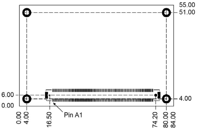
# 5.1 Module Size – Mini Module

The PCB size for the Mini Module shall be 84mm x 55mm. The PCB thickness should be 2mm to allow high layer count stack-ups and facilitate a standard ‘z’ dimension between the Carrier Board and the top of the heat-spreader (refer to Section 25 “Heat-Spreader“).

The holes shown in this drawing are intended for mounting the Module / heat-spreader combination to the Carrier Board. An independent, implementation specific set of holes and spacers may be used to attach the heat-spreader to the Module.

Figure 5-1: Mini Module Form Factor
![  Dimension   Value    --- ---    Top Section   55.00     Bottom Section   4.00     Middle Section   6.00     Right Section   51.00     Bottom Section (Pin A1)   16.50     Middle Section (Pin A1)   74.20     Right Section (Pin A1)   80.00     Bottom Section (Pin A1)   84.00  ](.picmg-com-0-r3-0-short-form-spec/9c495dc33df6cf4bb7483f17bbbe49577572b422fbf1ef64cf964310380d1129.jpg)

All dimensions are shown in millimeters.

# 5.2 Module Size - Compact Module

The PCB size for the Compact Module shall be 95mm x 95mm. The PCB thickness should be 2mm to allow high layer count stack-ups and facilitate a standard $' z '$ dimension between the Carrier Board and the top of the heat-spreader (refer to Section 25 “Heat-Spreader“).

The holes shown in this drawing are intended for mounting the Module / heat-spreader combination to the Carrier Board. An independent, implementation specific set of holes and spacers shall be used to attach the heat-spreader to the Module.

Figure 5-2: Compact Module Form Factor

# 5.3 Module Size - Basic Module

The PCB size for the Basic Module shall be 125mm x 95mm. The PCB thickness should be 2mm to allow high layer count stack-ups and facilitate a standard $' z '$ dimension between the Carrier Board and the top of the heat-spreader. (refer to Section 25 “Heat-Spreader“).

The holes shown in this drawing are intended for mounting the Module / heat-spreader combination to the Carrier Board. An independent, implementation specific set of holes and spacers shall be used to attach the heat-spreader to the Module.

Figure 5-3: Basic Module Form Factor

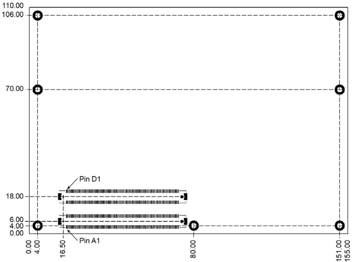
# 5.4 Module Size - Extended Module

The PCB size for the Extended Module shall be 155mm x 110mm. The PCB thickness should be 2mm to allow high layer count stack-ups and facilitate a standard $' z '$ dimension between the Carrier Board and the top of the heat-spreader. (refer to Section

# 25 “Heat-Spreader“).

The holes shown in this drawing are intended for mounting the Module / heat-spreader combination to the Carrier Board. An independent, implementation specific set of holes and spacers shall be used to attach the heat-spreader to the Module.

Figure 5-4: Extended Module Form Factor
![  Pin     X       Y        ------- ------- -------    Pin A1  4.00    4.00      Pin A1  8.00    6.00      Pin A1  16.50   18.00     Pin A1  80.00   4.00      Pin A1  151.00  4.00      Pin D1  4.00    70.00     Pin D1  80.00   18.00     Pin D1  151.00  106.00  ](.picmg-com-0-r3-0-short-form-spec/69d9985bc995965e57b5c899bd7cfe718a90892b334d7e602016ee759f4a0eb2.jpg)

All dimensions are shown in millimeters.

# 5.5 Module Connector

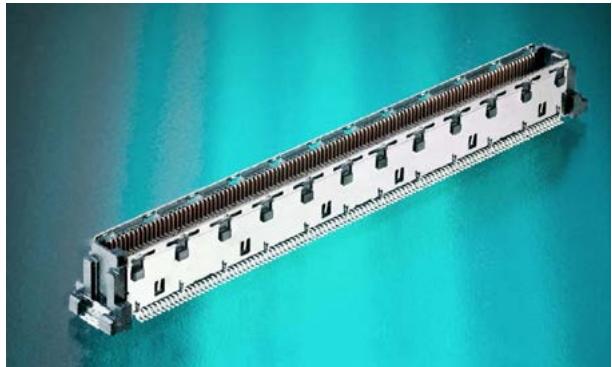
The Module connector for Pin-out Types 6 and 7 shall be a 440-pin receptacle that is composed of 2 pieces of a 220-pin, 0.5 mm pitch receptacle. The pair of connectors may be held together by a plastic carrier during assembly to allow handling by automated assembly equipment. Module Pin-out Type 10 shall use a single 220-pin, 0.5 mm pitch receptacle. The connectors shall be qualified for LVDS operation up to 6.25GHz and support for PCI Express Generation 3 signaling speeds.

The Module connector is a receptacle by virtue of the vendor’s technical definition of a receptacle, and to some users it looks like a plug.

Figure 5-5: Module Receptacle

# 5.6 Carrier Board Connector

The Carrier Board connector for Module Pin-out Types 6 and 7 shall be a 440-pin plug that is composed of 2 pieces of a 220-pin, 0.5 mm pitch plug. The pair of connectors may be held together by a plastic carrier during assembly to allow handling by automated assembly equipment.

The Carrier Board connector is a plug by virtue of the vendor’s technical definition of a plug, and to some users it looks like a receptacle.

Figure 5-6: Carrier Board Plug

![The image displays four technical line drawings of a long, rectangular mechanical component, likely a linear guide or rack assembly, arranged in a grid.  *   **Top Left:** A side elevation view showing the component's profile. It features a gear rack (a strip of teeth) at both the left and right ends, a long central section with a row of rectangular cutouts, and mounting brackets on the far ends. *   **Top Right:** An isometric view providing a 3D perspective of the assembly. It reveals the gear rack running along the top edge, the rectangular cutouts along the top surface, and the underlying base structure. *   **Bottom Left:** A view highlighting a central rod or shaft running longitudinally through the assembly. Gear rack mechanisms are visible at the ends, and a series of rectangular blocks or slots are aligned along the central guide. *   **Bottom Right:** An end elevation view showing the cross-section of one end of the component, detailing the mounting flanges and the profile of the gear teeth.](.picmg-com-0-r3-0-short-form-spec/3cace92a9c63c28af6431818f5c3dd93f9d4ba7842b53f1fe15348679ae03daa.jpg)

![3D rendering of a rectangular electronic component with multiple slots and mounting holes, placed on a teal surface (no text or symbols visible)](.picmg-com-0-r3-0-short-form-spec/db58d3c9df1ec5b9bd7d2318cfe4b19803d4df5d7dec2d5a2c1e243cfc508f5d.jpg)

# 5.7 Heat-Spreader

Modules should be equipped with a heat-spreader. This heat-spreader by itself does not constitute the complete thermal solution for a Module but provides a common interface between Modules and implementation-specific thermal solutions.

If implemented, a heat-spreader for the Compact, Basic and Extended form factor shall use and the Mini form factor may use an implementation specific set of holes and spacers to attach the heat-spreader to the Module. These implementation specific holes are in addition to the Module mounting holes specified in Sections 5.2, 5.3 or 5.4.

For the Compact, Basic and Extended form factor a heat-spreader should not use the Module mounting holes as the only attachment points to a Module. The intent is to be able to provide a Module and heat-spreader as an assembly that can then be mounted to a Carrier without having to break the thermal interface between the Module components and the heat-spreader.

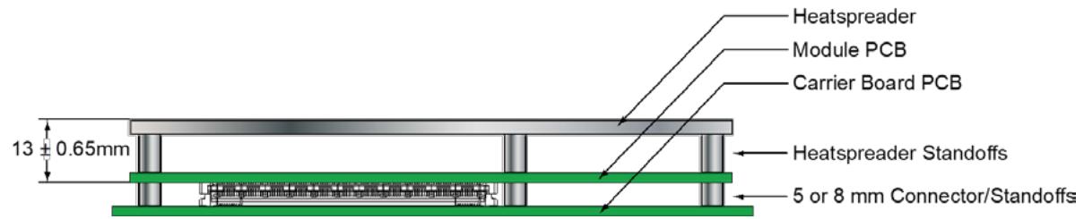
Figure 5-7: Overall Height for Heat-Spreader in Mini, Compact, Basic and Extended Modules
![Heatspreader Module PCB Carrier Board PCB 13 ± 0.65mm Heatspreader Standoffs 5 or 8 mm Connector/Standoffs](.picmg-com-0-r3-0-short-form-spec/fe4ef307f1996174c82bb56855d6a37ffa16cbfac6b545d077bef095c962cc93.jpg)

All dimensions in mm.

Figure 5-7 shows a cross section of a Module and heat-spreader assembled to a Carrier Board using the 5mm stack height option. If 8mm Carrier Board connectors are used, the overall assembly height increases from 18.00mm to 21.00mm.

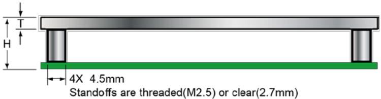
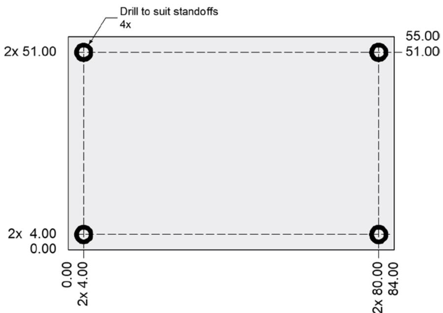
Figure 5-8: Mini Module Heat-Spreader
![T H 4X 4.5mm Standoffs are threaded(M2.5) or clear(2.7mm)](.picmg-com-0-r3-0-short-form-spec/1851306345001f163175700ad882109b28e27860fbe1d37bb6178fe6b773f6af.jpg)

Thickness‘T'is implemantation specific and may be 3mm. Height'H'(which includes PCB thickness) shallbe 13.00mm
![  Position   Dimension     :---   :---     Top Right   55.00     Bottom Right   51.00     Bottom Left   2x 4.00     Bottom Right   80.00     Bottom Left   2x 51.00     Bottom Right   2x 4.00     Bottom Left   0.00     Bottom Right   84.00   Drill to suit standoffs: 4x Drill to suit standoffs: 51.00](.picmg-com-0-r3-0-short-form-spec/e97b26e0011dc41aa5522f7541887c91a2a7c9290c194a1a8346c7c95602bac6.jpg)

All dimensions are in mm.

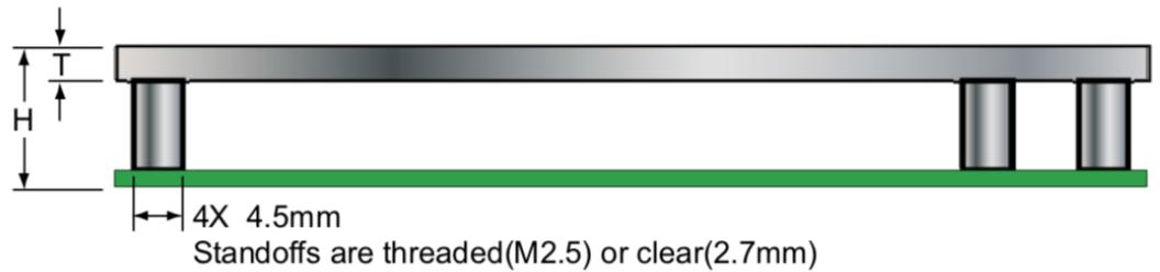
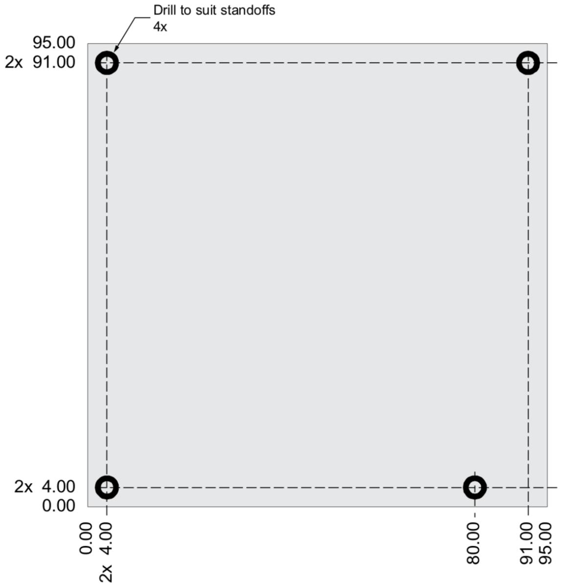
Figure 5-9: Compact Module Heat-Spreader
![T H 4X 4.5mm Standoffs are threaded(M2.5) or clear(2.7mm)](.picmg-com-0-r3-0-short-form-spec/0793867d889fa8286316a88012b9ba0835376d14bb7241ec62e89bb047790890.jpg)

Thickness ‘T' is implemantation specific and may be 3mm. Height 'H' (which includes PCB thickness) shall be 13.00mm
![  Position   Value    -------- -------    Top Right   95.00     Bottom Left   4.00     Bottom Right   4.00     Bottom Right   91.00  ](.picmg-com-0-r3-0-short-form-spec/bb66b712f4d668d4c12fe100368444f202c8d8857562d33e570b56f4fbc73826.jpg)

All dimensions are in mm.

Figure 5-10: Basic Module Heat-Spreader

![5X 4.5mm Standoffs are threaded(M2.5) or clear(2.7mm)](.picmg-com-0-r3-0-short-form-spec/0ccab71f289b443daef8d468d32d8c2f5b298150a0528f2ab5fe46b5f2f3365d.jpg)

Thickness ‘T'is implemantation specific and may be 3mm. Height 'H' (which includes PCB thickness) shall be 13.00mm
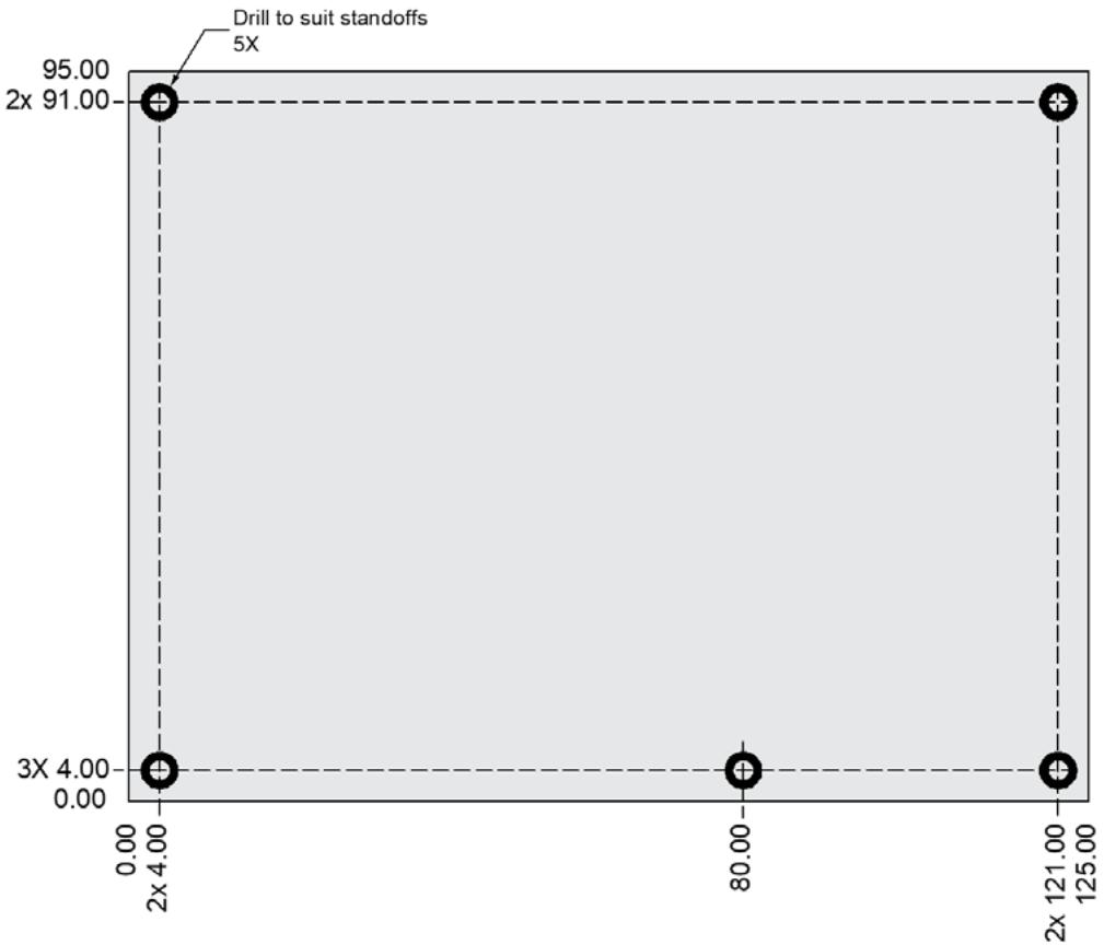
![  Position   Value    -------- -------    1        95.00     2        91.00     3        3X4.00     4        3X4.00     5        80.00     6        121.00     7        125.00  ](.picmg-com-0-r3-0-short-form-spec/5eb3e9848bb120cef00d196bad8b3fcef12ebf7e897924621add10a25b822251.jpg)

All dimensions are in mm.

Figure 5-11: Heat-Spreader Specification for Extended Module
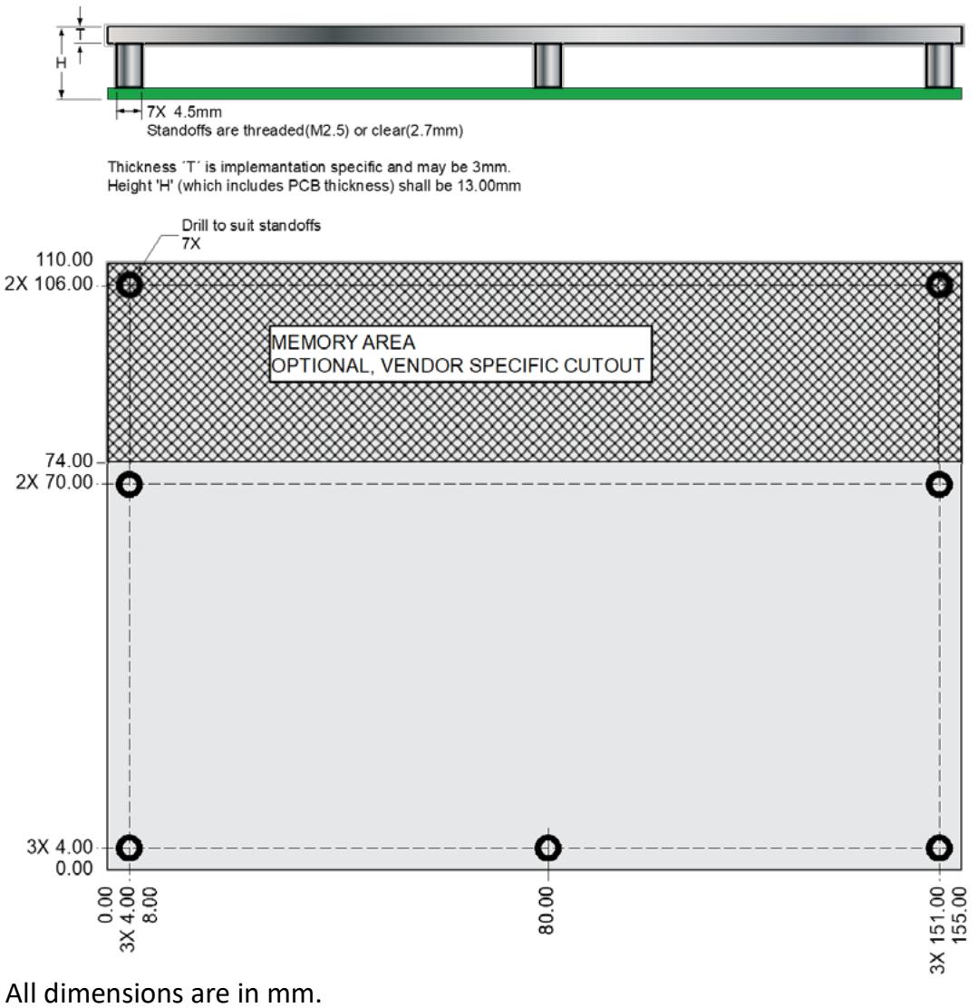
![7X 4.5mm Standoffs are threaded(M2.5) or clear(2.7mm) Thickness 'T' is implementation specific and may be 3mm. Height 'H' (which includes PCB thickness) shall be 13.00mm Drill to suit standoffs 7X 110.00 2X 106.00 MEMORY AREA OPTIONAL, VENDOR SPECIFIC CUTOUT 74.00 2X 70.00 3X 4.00 0.00 0.00 3X 4.00 8.00 80.00 3X 151.00 155.00 All dimensions are in mm.](.picmg-com-0-r3-0-short-form-spec/28fd9d1f86fd6698edf0ad5f73206cd0eacf82f8f71f0a91540557705a095f6b.jpg)

# 6 Electrical Specifications

# 6.1 Input Power - General Considerations

The Compact, Basic and Extended Module Modules shall use a single main power rail with a nominal value of +12V.

The Mini Module shall support a wide range power supply of 4.75V to 20.0V.

In addition, the Mini Module shall be optimized for 5V operation and Module vendors should report Module power figures at 5V, 12V and 18V input voltages.

Two additional rails are specified: a +5V standby power rail and a +3V battery input to power the Module Real-time Clock (RTC) circuit in the absence of other power sources.

The +5V standby rail may be left unconnected on the Carrier Board if the standby functions are not required by the application. Likewise, the +3V battery input may be left open if the application does not require the RTC to keep time in the absence of the main and standby sources.

The rationale for this power-delivery scheme is:

Module pins are scarce. It is more pin-efficient to bring power in on a higher voltage rail.
Single supply operation is attractive to many users.
Lithium ion battery packs for mobile systems are most prevalent with a +14.4V output. This is well suited for the +12V main power rail.
Contemporary chipsets have no power requirements for +5V other than to provide a reference voltage for +5V tolerant inputs. No COM Express Module pins are allocated to accept +5V except for the +5V standby pins. In the case of an ATX supply, the switched (non-standby) +5V line would not be used for the COM Express Module, but it might be used elsewhere on the Carrier Board.

# 7 Appendix

# 7.1 Mounting Positions and Connector Location for Carrier Boards

Figure 7-1: Carrier Board Mounting Positions

Common for all Form Factors
Extended only
Basic only
compact only
compact and Basic only
Mini only
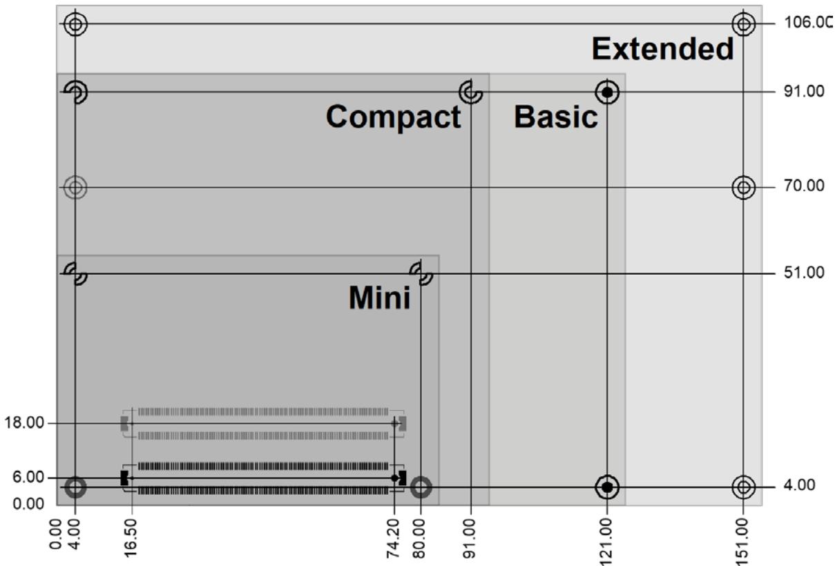
![  Category     Value      ----------   ------     Extended     106.00     Basic        91.00      Compact      70.00      Mini         4.00    ](.picmg-com-0-r3-0-short-form-spec/4239f7e049215f101bca8e834f56372eef9bdd8e492bdfd10dbb700fb77db526.jpg)

All dimensions are shown in millimeters.
[🔗 Link to the original document](.picmg-com-0-r3-0-short-form-spec/picmg-com-0-r3-0-short-form-spec.pdf)