# COM Express Carrier Design Guide
# COM Express® Carrier Design Guide
Guidelines for designing COM Express® Carrier Boards
December 6, 2013
# Rev. 2.0
This design guide is not a specification. It contains additional detail information but does not replace the PICMG COM Express® (COM.0) specification.
For complete guidelines on the design of COM Express® compliant Carrier Boards and systems, refer also to the full specification – do not use this design guide as the only reference for any design decisions. This design guide is to be used in conjunction with COM.0 R2.1.
© Copyright 2013, PCI Industrial Computer Manufacturers Group. The attention of adopters is directed to the possibility that compliance with or adoption of PICMG® specifications may require use of an invention covered by patent rights. PICMG® shall not be responsible for identifying patents for which a license may be required by any PICMG® specification or for conducting legal inquiries into the legal validity or scope of those patents that are brought to its attention.
PICMG® specifications are prospective and advisory only. Prospective users are responsible for protecting themselves against liability for infringement of patents.
# NOTICE:
The information contained in this document is subject to change without notice. The material in this document details a PICMG® specification in accordance with the license and notices set forth on this page. This document does not represent a commitment to implement any portion of this specification in any company's products.
WHILE THE INFORMATION IN THIS PUBLICATION IS BELIEVED TO BE ACCURATE, PICMG® MAKES NO WARRANTY OF ANY KIND, EXPRESS OR IMPLIED, WITH REGARD TO THIS MATERIAL INCLUDING, BUT NOT LIMITED TO, ANY WARRANTY OF TITLE OR OWNERSHIP, IMPLIED WARRANTY OF MERCHANTABILITY OR WARRANTY OF FITNESS FOR PARTICULAR PURPOSE OR USE.
In no event shall PICMG® be liable for errors contained herein or for indirect, incidental, special, consequential, reliance or cover damages, including loss of profits, revenue, data or use, incurred by any user or any third party. Compliance with this specification does not absolve manufacturers of equipment from the requirements of safety and regulatory agencies (UL, CSA, FCC, IEC, etc.).
# IMPORTANT NOTICE:
This document includes references to specifications, standards or other material not created by PICMG. Such referenced materials will typically have been created by organizations that operate under IPR policies with terms that vary widely, and under process controls with varying degrees of strictness and efficacy. PICMG has not made any enquiry into the nature or effectiveness of any such policies, processes or controls, and therefore ANY USE OF REFERENCED MATERIALS IS ENTIRELY AT THE RISK OF THE USER. Users should therefore make such investigations regarding referenced materials, and the organizations that have created them, as they deem appropriate.
PICMG®, CompactPCI®, AdvancedTCA®, AdvancedTCA® 300,ATCA®, ATCA® 300, AdvancedMC®, CompactPCI® Express, COM Express®, MicroTCA®, SHB Express®, and the PICMG, CompactPCI, AdvancedTCA, µTCA and ATCA logos are registered trademarks, and xTCA™, IRTM™ and the IRTM logo are trademarks of the PCI Industrial Computer Manufacturers Group. All other brand or product names may be trademarks or registered trademarks of their respective holders.
# Contents
# 1. Preface....................... 8
1.1. About This Document... 8
1.2. Intended Audience.... 8
1.3. No special word usage.. 8
1.4. No statements of compliance........... .. 8
1.5. Correctness Disclaimer.... .8
1.6. Name and logo usage.....
1.7. Intellectual property... .. 10
1.8. Acronyms, Abbreviations and Definitions Used... ..11
1.9. Signal Table Terminology........... .14
1.10. Schematic Conventions... .15
# 2. COM Express Interfaces.. ..16
2.1. COM Express Signals.. . 16
2.1.1. Connector Pin-out Comparison.. ..20
2.2. PCIe General Introduction.. .. 30
2.2.1. COM Express A-B Connector and C-D Connector PCIe Groups.. ..30
2.3. General Purpose PCIe Lanes... . 31
2.3.1. General Purpose PCIe Signal Definitions.. ..31
2.3.2. PCI Express Lane Configurations – Per COM Express Spec. ..32
2.3.3. PCI Express Lane Configurations – Module and Chipset Dependencies.. ..32
2.3.4. Device Up / Device Down and PCIe Rx / Tx Coupling Capacitors.. ..33
2.3.5. Schematic Examples.. ..34
2.3.6. PCI Express Routing Considerations... ..47
2.4. PEG (PCI Express Graphics).. .. 48
2.4.1. Signal Definitions.. ..48
2.4.2. PEG Configuration.. ..49
2.4.3. Reference Schematics.. ..52
2.4.4. Routing Considerations.. ..53
2.5. Digital Display Interfaces..... . 55
2.5.1. DisplayPort / HDMI / DVI . ..55
2.5.2. SDVO.... ..61
2.6. Mobile PCI Express Module (MXM)... .. 66
2.6.1. Signal Definitions.. ..66
2.6.2. Reference Schematics. ..68
2.6.3. Routing Considerations.. ..69
2.7. LAN.... .. 70
2.7.1. Signal Definitions.. ..70
2.7.2. Reference Schematics.. ..73
2.7.3. Routing Considerations.. ..75
2.8. USB Ports.... .. 76
2.8.1. Signal Definitions.. ..76
2.8.2. Reference Schematics. ..77
2.8.3. Avoiding Back-driving Problems.. ..80
2.8.4. Routing Considerations.. ..80
# 2.9. USB 3.0.. .81
2.9.1. Signal Definitions.. ..81
2.9.2. Reference Schematics.. ..84
2.9.3. Avoiding Back-driving Problems.. ..86
2.9.4. Routing Considerations.. ..86
# 2.10. SATA... . 87
2.10.1. Signal Definitions.. ..87
2.10.2. Reference Schematic.. ..89
2.10.3. Routing Considerations.. ..90
# 2.11. LVDS... .91
2.11.1. Signal Definitions.. ..91
2.11.2. Reference Schematics.. ..97
2.11.3. Routing Considerations.. ..98
# 2.12. Embedded DisplayPort (eDP)... .99
2.12.1. Signal Definitions.. ..99
2.12.2. Reference Schematics.. ..100
2.12.3. Routing Considerations.. ..100
# 2.13. VGA.... ... 101
2.13.1. Signal Definitions.. ..101
2.13.2. VGA Connector... ...101
2.13.3. VGA Reference Schematics.. ..102
2.13.4. Routing Considerations.. .103
# 2.14. TV-Out..... ..... 104
# 2.15. Digital Audio Interfaces.. .. 105
2.15.1. Reference Schematics.. ..107
# 2.16. LPC Bus – Low Pin Count Interface........... ......... 111
2.16.1. Signal Definition.. .111
2.16.2. LPC Bus Reference Schematics. ..111
2.16.3. Routing Considerations.. ..116
# 2.17. SPI – Serial Peripheral Interface Bus....... .... 118
2.17.1. Signal Definition.. ..118
2.17.2. SPI Reference Schematics.. ..119
2.17.3. Routing Considerations.. ..120
# 2.18. General Purpose I2C Bus Interface....... ... 121
2.18.1. Signal Definitions.. ..121
2.18.2. Reference Schematics.. ..121
2.18.3. Connectivity Considerations.. ..122
# 2.19. System Management Bus (SMBus)... .. 123
2.19.1. Signal Definitions.. ..123
2.19.2. Routing Considerations.. ..124
# 2.20. General Purpose Serial Interface........... .... 125
2.20.1. Signal Definitions.. ..125
2.20.2. Reference Schematics.. ..126
2.20.3. Routing Considerations. .126
# 2.21. CAN Interface.... .. 127
2.21.1. Signal Definitions.. ..127
2.21.2. Reference Schematics.. .128
2.21.3. Routing Considerations.. ..128
# 2.22. Miscellaneous Signals.. ..129
2.22.1. Module Type Detection.. ..130
2.22.2. Speaker Output.. ..130
2.22.3. RTC Battery Implementation. ..131
2.22.4. Power Management Signals.. ..133
2.22.5. Watchdog Timer.. ..135
2.22.6. General Purpose Input/Output (GPIO).. ..136
2.22.7. SDIO Interface Multiplexed with GPIOs.. ..138
2.22.8. Fan Connector........ ...140
2.22.9. Thermal Interface.. ..141
2.22.10. Protecting COM.0 Pins Reclaimed From the VCC\_12V Pool.. ..142
# 2.23. PCI Bus.... .. 145
2.23.1. Signal Definitions.. .145
2.23.2. Reference Schematics.. ..146
2.23.3. Routing Considerations.. ..149
# 2.24. IDE and CompactFlash (PATA)...... ... 151
2.24.1. Signal Definitions... ...151
2.24.2. IDE 40-Pin Header (3.5 Inch Drives).. ..152
2.24.3. IDE 44-Pin Header (2.5 Inch and Low Profile Optical Drives).. ..152
2.24.4. CompactFlash 50 Pin Header.. ..152
2.24.5. IDE / CompactFlash Reference Schematics.. ..152
2.24.6. Routing Considerations.. ..153
# 3. Power and Reset... ..154
# 3.1. General Power requirements.. .. 154
3.1.1. VCC\_12V Rise Time Caution and Inrush Currents.. ..154
# 3.2. ATX and AT Style Power Control.. .. 155
3.2.1. ATX vs AT Supplies.. ..155
3.2.2. Power States.. ..155
3.2.3. ATX and AT Power Sequencing Diagrams... ...156
3.2.4. Power Monitoring Circuit Discussion.. ..159
3.2.5. Power Button... ..160
# 3.3. Design Considerations for Carrier Boards containing FPGAs/CPLDs....... .....161
# 3.4. Reference Schematics.. .. 162
3.4.1. ATX Power Supply.. ..162
# 3.5. Routing Considerations........ ...... 165
3.5.1. VCC\_12V and GND.. ..165
3.5.2. Copper Trace Sizing and Current Capacity.. ..165
3.5.3. VCC5\_SBY Routing... ..166
3.5.4. Power State and Reset Signal Routing....... ....166
3.5.5. Slot Card Supply Decoupling Recommendations.. ...167
# 4. BIOS Considerations.... ...168
# 4.1. Legacy versus Legacy-Free.. .. 168
4.2. Super I/O.... ... 168
5. COM Express Module Connectors..... ....169
5.1. Connector Descriptions...... ... 169
5.2. Connector Land Patterns and Alignment.. ... 169
5.3. Connector and Module CAD Symbol Recommendations..... .....170
6. Carrier Board PCB Layout Guidelines.... ..171
6.1. General.. .. 171
6.2. PCB Stack-ups..... ... 171
6.2.1. Four-Layer Stack-up.. .171
6.2.2. Six-Layer Stack-up.. .171
6.2.3. Eight-Layer Stack-up.. ..172
6.3. Trace-Impedance Considerations... .. 173
6.4. Trace-Length Extensions Considerations....... ... 175
6.5. Routing Rules for High-Speed Differential Interfaces...... ...176
6.5.1. PCI Express Trace Routing Guidelines... ..178
6.5.2. USB Trace Routing Guidelines. ..179
6.5.3. USB 3.0 Trace Routing Guidelines... ...180
6.5.4. PEG Trace Routing Guidelines.. ..180
6.5.5. SDVO Trace Routing Guidelines. .181
6.5.6. DisplayPort Trace Routing Guidelines.. ..182
6.5.7. LAN Trace Routing Guidelines.. ..183
6.5.8. Serial ATA Trace Routing Guidelines.. ..184
6.5.9. LVDS Trace Routing Guidelines.. ..185
6.6. Routing Rules for Single Ended Interfaces...... .... 186
6.6.1. PCI Trace Routing Guidelines.. ..187
6.6.2. IDE Trace Routing Guidelines.. ..188
6.6.3. LPC Trace Routing Guidelines.. ..189
7. Mechanical Considerations....................
7.1. Form Factors..................... ...... 190
7.2. Heatspreader... ..191
7.2.1. Top mounting.. .192
7.2.2. Bottom mounting.. ..193
7.2.3. Materials.. ..193
8. Applicable Documents and Standards...... ...195
8.1. Technology Specifications...... ... 195
8.2. Regulatory Specifications... .. 197
8.3. Useful books.... .. 198
9. Appendix A: Deprecated Features.... ..199
9.1. TV-Out... . 199
9.1.1. Signal Definitions.. .199
9.1.2. TV-Out Connector.. ..199
9.1.3. TV-Out Reference Schematics.. .201
9.1.4. Routing Considerations... ..202
9.1.5. Signal Termination.. ..202
9.1.6. Video Filter... ..202
9.1.7. ESD Protection.. ..202
# 9.2. LPC Firmware Hub..... .. 203
10. Appendix B: Sourcecode for Port 80 Decoder...... ..205
11. Appendix C: List of Tables..... ..209
12. Appendix D: List of Figures...... ..211
13. Appendix E: Revision History..................... ...213
# 1. Preface
# 1.1. About This Document
This document provides information for designing a custom system Carrier Board for COM Express Modules. It includes reference schematics for the external circuitry required to implement the various COM Express peripheral functions. It also explains how to extend the supported buses and how to add additional peripherals and expansion slots to a COM Express based system.
It's strongly recommended to use the latest COM Express specification and the Module vendors' product manuals as a reference.
This design guide is not a specification. It contains additional detail information but does not replace the PICMG COM Express (COM.0) specification.
For complete guidelines on the design of COM Express compliant Carrier Boards and systems, refer also to the full specification – do not use this design guide as the only reference for any design decisions.
# 1.2. Intended Audience
This design guide is intended for electronics engineers and PCB layout engineers designing Carrier Boards for PICMG COM Express Modules.
# 1.3. No special word usage
Unlike a PICMG specification, which assigns special meanings to certain words such as ”shall”, “should” and “may”, there is no such usage in this document. That is because this document is not a specification; it is a non-normative design guide.
# 1.4. No statements of compliance
As this document is not a specification but a set of guidelines, there should not be any statements of compliance made with reference to this document.
# 1.5. Correctness Disclaimer
The schematic examples given in this document are believed to be correct but no guarantee is given. In most cases, the examples come from designs that have been built and tested.
# 1.6. Name and logo usage
The PCI Industrial Computer Manufacturers Group’s policies regarding the use of its logos and trademarks are as follows:
Permission to use the PICMG organization logo is automatically granted to designated members only as stipulated on the most recent Membership Privileges document (available at www.picmg.org) during the period of time for which their membership dues are paid. Nonmembers must not use the PICMG organization logo.
The PICMG organization logo must be printed in black or color as shown in the files available for download from the member’s side of the Web site. Logos with or without the “Open Modular Computing Specifications” banner can be used. Nothing may be added or deleted from the PICMG logo.
The use of the COM Express logo is a privilege granted by the PICMG® organization to companies who have purchased the relevant specifications (or acquired them as a member benefit), and that believe their products comply with these specifications. Manufacturers' distributors and sales representatives may use the COM Express logo in promoting products sold under the name of the manufacturer. Use of the logos by either members or non-members implies such compliance. Only PICMG Executive and Associate members may use the PICMG® logo. PICMG® may revoke permission to use logos if they are misused. The COM Express logo can be found on the PICMG web site, www.picmg.org.
The PICMG® name and logo and the COM Express name and logo are registered trademarks of PICMG®. Registered trademarks must be followed by the ® symbol, and the following statement must appear in all published literature and advertising material in which the logo appears:
PICMG, the COM Express name and logo and the PICMG logo are registered trademarks of the PCI Industrial Computers Manufacturers Group.
# 1.7. Intellectual property
The Consortium draws attention to the fact that implementing recommendations made in this document could involve the use of one or more patent claims (“IPR”). The Consortium takes no position concerning the evidence, validity, or scope of this IPR.
Attention is also drawn to the possibility that implementation of some of the elements in this document could be the subject of unidentified IPR. The Consortium is not responsible for identifying any or all such IPR.
No representation is made as to the availability of any license rights for use of any IPR that might be required to implement the recommendations of this Guide. This document conforms to the current PICMG Intellectual Property Rights Policy and the Policies and Procedures for Specification Development and does not contain any known intellectual property that is not available for licensing under Reasonable and Nondiscriminatory terms. In the course of Membership Review the following disclosures were made:
Necessary Claims (referring to mandatory or recommended features):
None.
Unnecessary Claims (referring to optional features or non-normative elements):
None.
Third Party Disclosures (Note that third party IPR submissions do not contain any claim of willingness to license the IPR:
None.
# Note:
This document is being offered without any warranty whatsoever, and in particular, any warranty of non-infringement is expressly disclaimed. Any use of this document shall be made entirely at the implementer's own risk, and neither the consortium, nor any of its members or submitters, shall have any liability whatsoever to any implementer or third party for any damages of any nature whatsoever, directly or indirectly, arising from the use of this document.
Copyright Notice
Copyright © 2013, PICMG. All rights reserved. All text, pictures and graphics are protected by copyrights. No copying is permitted without written permission from PICMG.
PICMG has made every attempt to ensure that the information in this document is accurate yet the information contained within is supplied “as-is”.
Trademarks
Intel and Pentium are registered trademarks of Intel Corporation. ExpressCard is a registered trademark of Personal Computer Memory Card International Association (PCMCIA). PCI Express is a registered trademark of Peripheral Component Interconnect Special Interest Group (PCI-SIG). COM Express is a registered trademark of PCI Industrial Computer Manufacturers Group (PICMG). I2C is a registered trademark of NXP Semiconductors. CompactFlash is a registered trademark of CompactFlash Association. Winbond is a registered trademark of Winbond Electronics Corp. AVR is a registered trademark of Atmel Corporation. Microsoft®, Windows®, Windows NT®, Windows CE and Windows XP® are registered trademarks of Microsoft Corporation. VxWorks is a registered trademark of WindRiver. All product names and logos are property of their owners.
# 1.8. Acronyms, Abbreviations and Definitions Used
Table 1: Acronyms, Abbreviations and Definitions Used
| Term | Description |
| AC '97 / HDA | Audio CODEC '97/High Definition Audio |
| ACPI | Advanced Configuration Power Interface – standard to implement power saving modes in PCAT systems |
| ADD2 | Advanced Digital Display, $2^{nd}$ Generation |
| ADD2/MEC | Advanced Digital Display, $2^{nd}$ Generation, Media Expansion Card |
| Basic Module | COM Express® 125mm x 95mm Module form factor. |
| BIOS | Basic Input Output System – firmware in PC-AT system that is used to initialize system components before handing control over to the operating system. |
| CAN | Controller-area network (CAN or CAN-bus) is a vehicle bus standard designed to allow microcontrollers to communicate with each other within a vehicle without a host computer. |
| Carrier Board | An application specific circuit board that accepts a COM Express® Module. |
| Compact Module | COM Express® 95mm x 95mm Module form factor |
| CRT | Cathode Ray Tube |
| DAC | Digital Analog Converter |
| DDC | Display Data Control – VESA (Video Electronics Standards Association) standard to allow identification of the capabilities of a VGA monitor |
| DDI | Digital Display Interface– containing DisplayPort, HDMI/DVI and SDVO |
| DNI | Do Not Install |
| DP | DisplayPort is a digital display interface standard put forth by the Video Electronics Standards Association (VESA). It defines a new license free, royalty free, digital audio/video interconnect, intended to be used primarily between a computer and its display monitor. |
| DVI | Digital Visual Interface - a Digital Display Working Group (DDWG) standard that defines a standard video interface supporting both digital and analog video signals. The digital signals use TMDS. |
| EAPI | Embedded Application Programming InterfaceSoftware interface for COM Express® specific industrial functionsSystem informationWatchdog timerI2C BusFlat Panel brightness controlUser storage areaGPIO |
| EDID | Extended Display Identification Data |
| EDP | Embedded DisplayPort (eDP) is a digital display interface standard produced by the Video Electronics Standards Association (VESA) for digital interconnect of Audio and Video. |
| EEPROM | Electrically Erasable Programmable Read-Only Memory |
| EFT | Electrical Fast Transient |
| EMI | Electromagnetic Interference |
| ESD | Electrostatic Discharge |
| ExpressCard | A PCMCIA standard built on the latest USB 2.0 and PCI Express buses. |
| Extended Module | COM Express® 155mm x 110mm Module form factor. |
| FR4 | A type of fiber-glass laminate commonly used for printed circuit boards. |
| Gb | Gigabit |
| GbE | Gigabit Ethernet |
| GPI | General Purpose Input |
| GPIO | General Purpose Input Output |
| GPO | General Purpose Output |
| HDA | Intel High Definition Audio (HD Audio) refers to the specification released by Intel in 2004 for delivering high definition audio that is capable of playing back more channels at higher quality than AC97. |
| HDMI | High Definition Multimedia Interface |
| I2C | Inter Integrated Circuit - 2 wire (clock and data) signaling scheme allowing communication between integrated circuits, primarily used to read and load register values. |
| IDE | Integrated Device Electronics - parallel interface for hard disk drives - also known as PATA |
| Legacy Device | Relics from the PC-AT computer that are not in use in contemporary PC systems: primarily the ISA bus, UART-based serial ports, parallel printer ports, PS-2 keyboards, and mice.Definitions vary as to what constitutes a legacy device. Some definitions include IDE as a legacy device. |
| LAN | Local Area Network |
| LPC | Low Pin-Count Interface: a low speed interface used for peripheral circuits such as Super I/O controllers, which typically combine legacy-device support into a single IC. |
| LS | Least Significant |
| LVDS | Low-Voltage Differential Signaling - widely used as a physical interface for TFT flat panels.LVDS can be used for many high-speed signaling applications. In this document, it refers only to TFT flat-panel applications. |
| MEC | Media Expansion Card |
| Mini Module | COM Express® 84x55mm Module form factor |
| MS | Most Significant |
| NA | Not available |
| NC | Not connected |
| OBD-II | On-Board Diagnostics $2^{nd}$ generation |
| OEM | Original Equipment Manufacturer |
| PATA | Parallel AT Attachment - parallel interface standard for hard-disk drives - also known as IDE, AT Attachment, and as ATA |
| PC-AT | “Personal Computer - Advanced Technology” - an IBM trademark term used to refer to Intel x86 based personal computers in the 1990s |
| PCB | Printed Circuit Board |
| PCI | Peripheral Component Interface |
| PCI Express (PCIe) | Peripheral Component Interface Express - next-generation high speed Serialized I/O bus |
| PCI Express Lane | One PCI Express Lane is a set of 4 signals that contains two differential lines for Transmitter and two differential lines for Receiver. Clocking information is embedded into the data stream. |
| PD | Pull Down |
| PEG | PCI Express Graphics |
| PHY | Ethernet controller physical layer device |
| Pin-out Type | A reference to one of seven COM Express® definitions for the signals that appear on the COM Express® Module connector pins. |
| PS2PS2 KeyboardPS2 Mouse | “Personal System 2” - an IBM trademark term used to refer to Intel x86 based personal computers in the 1990s. The term survives as a reference to the style of mouse and keyboard interface that were introduced with the PS2 system. |
| PU | Pull Up |
| ROM | Read Only Memory - a legacy term - often the device referred to as a ROM can actually be written to, in a special mode. Such writable ROMs are sometimes called Flash ROMs. BIOS is stored in ROM or Flash ROM. |
| RTC | Real Time Clock - battery backed circuit in PC-AT systems that keeps system time and date as well as certain system setup parameters |
| S0, S1, S2, S3, S4, S5 | Sleep States defined by the ACPI specificationS0 Full power, all devices poweredS1Sleep State, all context maintainedS2 Sleep State, CPU and Cache context lostS3 Suspend to RAM System context stored in RAM; RAM is in standbyS4 Suspend to Disk System context stored on diskS5 Soft Off Main power rail off, only standby power rail present |
| SATA | Serial AT Attachment: serial-interface standard for hard disks |
| SDVO | Serial Digital Video Out is a proprietary technology introduced by Intel® to add additional video signaling interfaces to a system. Being phased out |
| SMBus | System Management Bus |
| SO-DIMM | Small Outline Dual In-line Memory Module |
| SPI | Serial Peripheral Interface |
| TBD | To be determined |
| TMDS | Transition Minimized Differential Signaling - a digital signaling protocol between the graphics subsystem and display. TMDS is used for the DVI digital signals. DC coupled |
| TPM | Trusted Platform Module, chip to enhance the security features of a computer system. |
| UIM | User Identity Module |
| USB | Universal Serial Bus |
| VESA | Video Electronics Standards Association |
| WDT | Watch Dog Timer |
# 1.9. Signal Table Terminology
Table 2 below describes the terminology used in this section for the Signal Description tables. The $" \# "$ symbol at the end of the signal name indicates that the active or asserted state occurs when the signal is at a low voltage level. When “#” is not present, the signal is asserted when at a high voltage level.
The terms “Input” and “Output” and their abbreviations in Table 2 below refer to the Module's view, i.e. an input is an input for the Module and not for the Carrier-Board.
Table 2: Signal Table Terminology Descriptions
| Term | Description |
| I/O 3.3V | Bi-directional signal 3.3V tolerant |
| I/O 5V | Bi-directional signal 5V tolerant |
| I 3.3V | Input 3.3V tolerant |
| I 5V | Input 5V tolerant |
| I/O 3V3_SBY | Bi-directional 3.3V tolerant active during Suspend and running state. |
| O 3.3V | Output 3.3V signal level |
| O 5V | Output 5V signal level |
| OD | Open drain output |
| P | Power input/output |
| *_S0 | Signal active during running state. |
| PCIE | In compliance with PCI Express Base Specification |
| USB | In compliance with the Universal Serial Bus Specification |
| GbE | In compliance with IEEE 802.3ab 1000BASE-T Gigabit Ethernet |
| SATA | In compliance with Serial ATA specification |
| REF | Reference voltage output. May be sourced from a Module power plane. |
| PDS | Pull-down strap. A Module output pin that is either tied to GND or is not connected. Used to signal Module capabilities (pin-out type) to the Carrier Board. |
# 1.10. Schematic Conventions
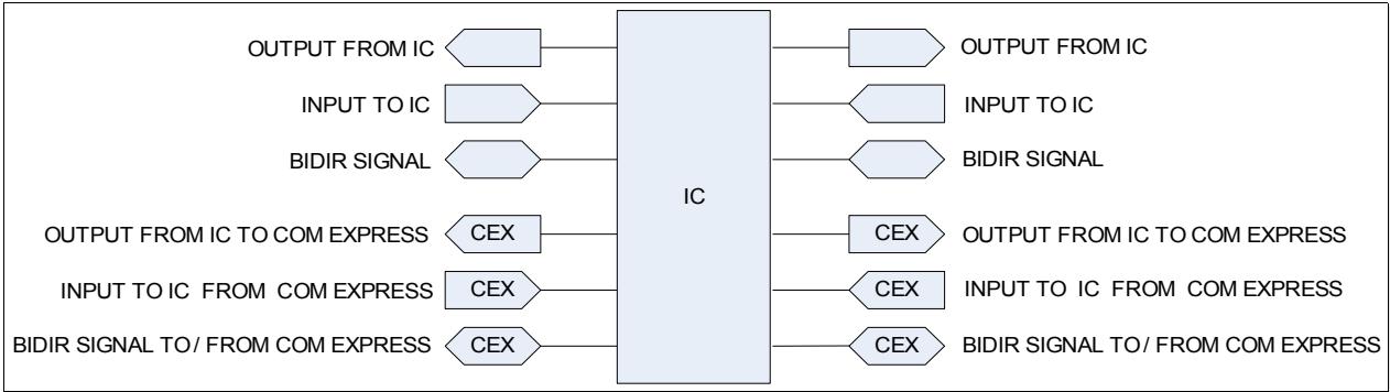
Schematic examples are drawn with signal directions shown per the figure below. Signals that connect directly to the COM Express connector are flagged with the text “CEX” in the off-page connect symbol, as shown in Figure 1 below. Nets that connect to the COM Express Module are named per the PICMG COM Express specification.
Figure 1: Schematic Conventions
Power nets are labeled per the table below. The power rail behavior under the various system power states is shown in the table.
Table 3: Naming of Power Nets
| Power Net | S0 On | S3 Suspend to RAM | S4 Suspend to Disk | S5 Soft Off | G3 Mechanical Off |
| VCC_12V | 12V | off | off | off | off |
| VCC_5V0 | 5V | off | off | off | off |
| VCC_3V3 | 3.3V | off | off | off | off |
| VCC_1V5 | 1.5V | off | off | off | off |
| VCC_2V5 | 2.5V | off | off | off | off |
| VCC_5V_SBY | 5V | 5V | 5V | 5V | off |
| VCC_3V3_SBY | 3.3V | 3.3V | 3.3V | 3.3V | off |
| VCC_RTC | 3.0V | 3.0V | 3.0V | 3.0V | 3.0V |
# 2. COM Express Interfaces
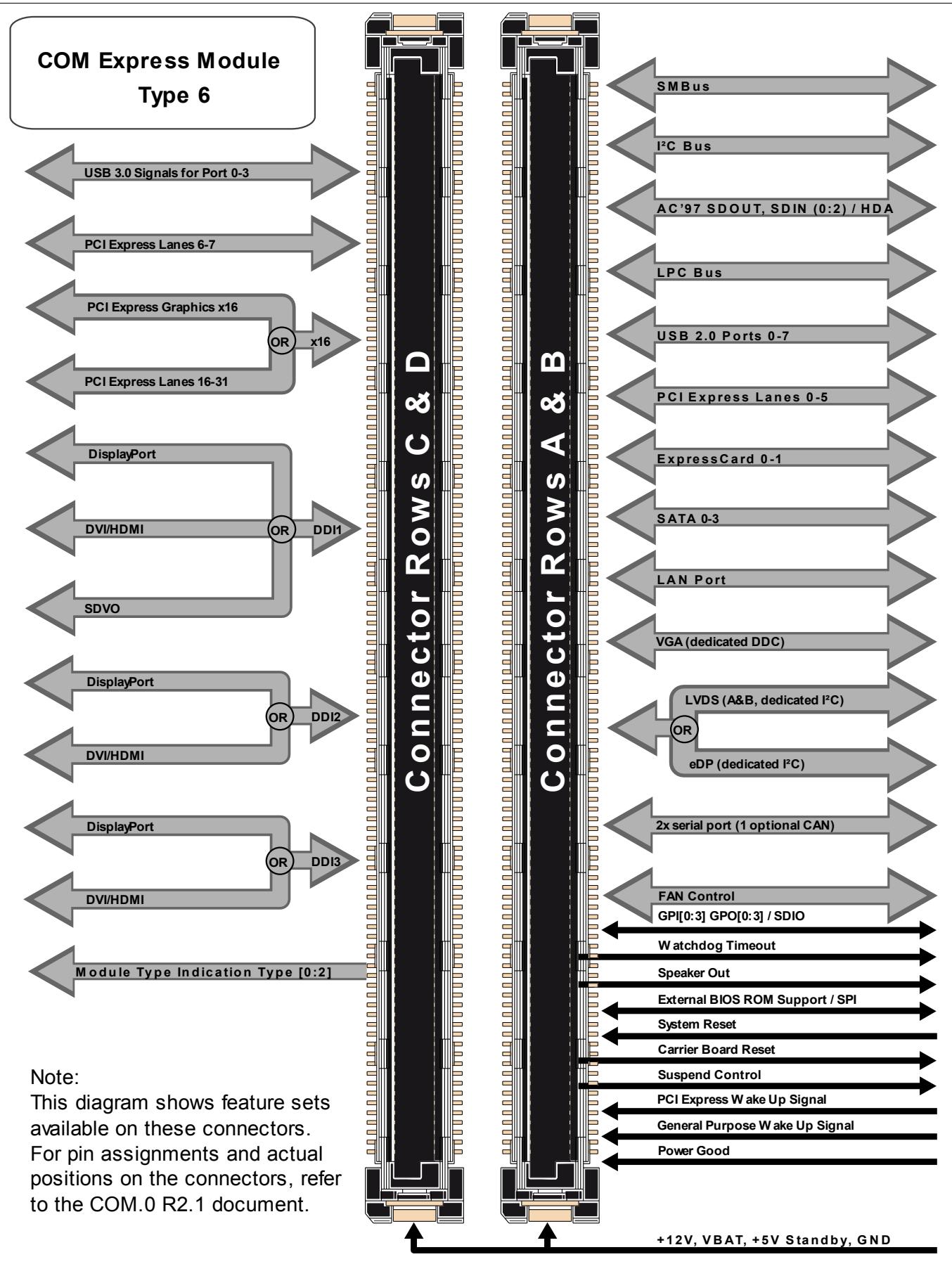
The following section summarizes the signals found on COM Express Type 10, Type 2 and Type 6 connectors. Most of the signals listed in the following sections also apply to other COM Express Module types. The pin-out for connector rows A and B remains mostly the same regardless of the Module type but the pin-out for connector rows D and C are dependent on the Module type. Refer to the COM Express Specification for information about the different pin-outs of the Module types other than Type 10, 2 and 6.
With some planning and forethought by the Carrier Board designer, it is possible to create dual use layouts that can accommodate Type 10 and Type 6 or Type 10 and Type 2, if desired.
# 2.1. COM Express Signals
The source document for the definition of the COM Express signals is the PICMG COM.0 R2.1 COM Express Module Base Specification.
Figure 2, Figure 3 and Figure 4 below summarizes the Type 10, Type 2 and Type 6 signals and show a graphical representation of the A-B and C-D COM Express connectors. Each of the signal groups in the figure is described and usage examples are given in the sub-sections of this section.
Figure 2: COM Express Type 10 Connector Layout
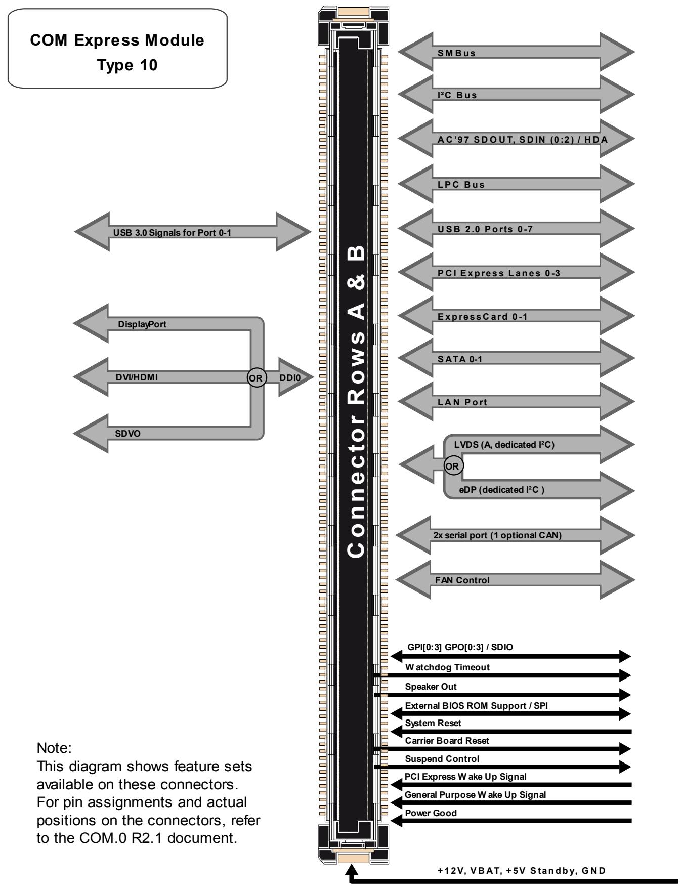
Figure 3: COM Express Type 2 Connector Layout
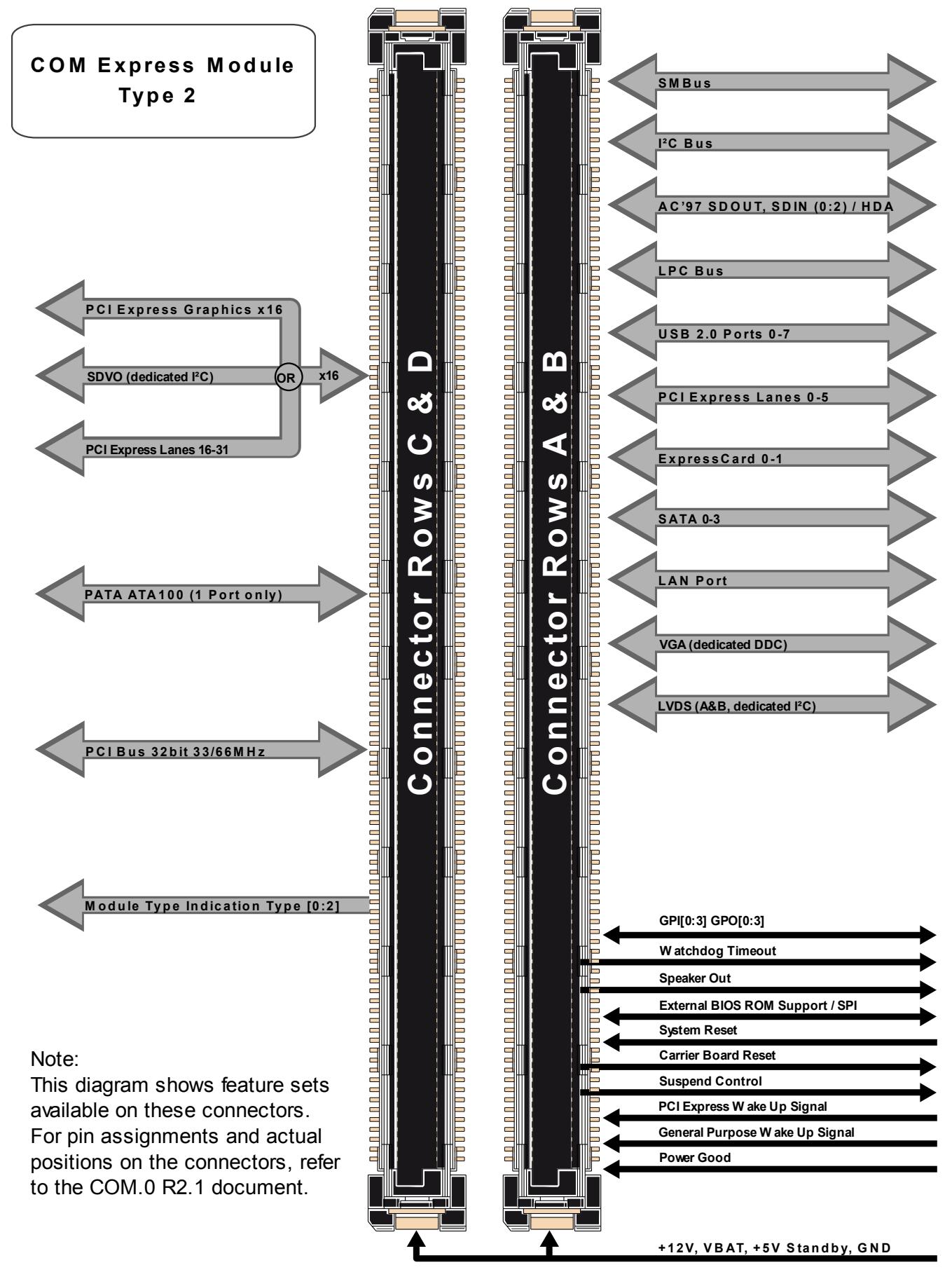
Figure 4: COM Express Type 6 Connector Layout
# 2.1.1. Connector Pin-out Comparison
Table 4: Pin-out Comparison
| Pin# | Type 10 Description | Type 2 Description | Type 6 Description |
| A1 | GND(FIXED) | GND(FIXED) | GND(FIXED) |
| A2 | GBE0_MDI3- | GBE0_MDI3- | GBE0_MDI3- |
| A3 | GBE0_MDI3+ | GBE0_MDI3+ | GBE0_MDI3+ |
| A4 | GBE0_LINK100# | GBE0_LINK100# | GBE0_LINK100# |
| A5 | GBE0_LINK1000# | GBE0_LINK1000# | GBE0_LINK1000# |
| A6 | GBE0_MDI2- | GBE0_MDI2- | GBE0_MDI2- |
| A7 | GBE0_MDI2+ | GBE0_MDI2+ | GBE0_MDI2+ |
| A8 | GBE0_LINK# | GBE0_LINK# | GBE0_LINK# |
| A9 | GBE0_MDI1- | GBE0_MDI1- | GBE0_MDI1- |
| A10 | GBE0_MDI1+ | GBE0_MDI1+ | GBE0_MDI1+ |
| A11 | GND(FIXED) | GND(FIXED) | GND(FIXED) |
| A12 | GBE0_MDI0- | GBE0_MDI0- | GBE0_MDI0- |
| A13 | GBE0_MDI0+ | GBE0_MDI0+ | GBE0_MDI0+ |
| A14 | GBE0_CTREF | GBE0_CTREF | GBE0_CTREF |
| A15 | SUS_S3# | SUS_S3# | SUS_S3# |
| A16 | SATA0_TX+ | SATA0_TX+ | SATA0_TX+ |
| A17 | SATA0_TX- | SATA0_TX- | SATA0_TX- |
| A18 | SUS_S4# | SUS_S4# | SUS_S4# |
| A19 | SATA0_RX+ | SATA0_RX+ | SATA0_RX+ |
| A20 | SATA0_RX- | SATA0_RX- | SATA0_RX- |
| A21 | GND(FIXED) | GND(FIXED) | GND(FIXED) |
| A22 | USB_SSRX0- | SATA2_TX+ | SATA2_TX+ |
| A23 | USB_SSRX0+ | SATA2_TX- | SATA2_TX- |
| A24 | SUS_S5# | SUS_S5# | SUS_S5# |
| A25 | USB_SSRX1- | SATA2_RX+ | SATA2_RX+ |
| A26 | USB_SSRX1+ | SATA2_RX- | SATA2_RX- |
| A27 | BATLOW# | BATLOW# | BATLOW# |
| A28 | (S)ATA_ACT# | (S)ATA_ACT# | (S)ATA_ACT# |
| A29 | AC/HDA_SYNC | AC/HDA_SYNC | AC/HDA_SYNC |
| A30 | AC/HDA_RST# | AC/HDA_RST# | AC/HDA_RST# |
| A31 | GND(FIXED) | GND(FIXED) | GND(FIXED) |
| A32 | AC/HDA_BITCLK | AC/HDA_BITCLK | AC/HDA_BITCLK |
| A33 | AC/HDA_SDOUT | AC/HDA_SDOUT | AC/HDA_SDOUT |
| A34 | BIOS_DIS0# | BIOS_DIS0# | BIOS_DIS0# |
| A35 | THRMTRIP# | THRMTRIP# | THRMTRIP# |
| A36 | USB6- | USB6- | USB6- |
| A37 | USB6+ | USB6+ | USB6+ |
| A38 | USB_6_7_OC# | USB_6_7_OC# | USB_6_7_OC# |
| A39 | USB4- | USB4- | USB4- |
| A40 | USB4+ | USB4+ | USB4+ |
| A41 | GND(FIXED) | GND(FIXED) | GND(FIXED) |
| A42 | USB2- | USB2- | USB2- |
| A43 | USB2+ | USB2+ | USB2+ |
| A44 | USB_2_3_OC# | USB_2_3_OC# | USB_2_3_OC# |
| A45 | USB0- | USB0- | USB0- |
| A46 | USB0+ | USB0+ | USB0+ |
| A47 | VCC_RTC | VCC_RTC | VCC_RTC |
| A48 | EXCD0_PERST# | EXCD0_PERST# | EXCD0_PERST# |
| A49 | EXCD0_CPPE# | EXCD0_CPPE# | EXCD0_CPPE# |
| A50 | LPC_SERIRQ | LPC_SERIRQ | LPC_SERIRQ |
| A51 | GND(FIXED) | GND(FIXED) | GND(FIXED) |
| A52 | RSVD | PCIE_TX5+ | PCIE_TX5+ |
| A53 | RSVD | PCIE_TX5- | PCIE_TX5- |
| A54 | GPIO | GPIO | GPIO |
| A55 | RSVD | PCIE_TX4+ | PCIE_TX4+ |
| A56 | RSVD | PCIE_TX4- | PCIE_TX4- |
| A57 | GND | GND | GND |
| A58 | PCIE_TX3+ | PCIE_TX3+ | PCIE_TX3+ |
| A59 | PCIE_TX3- | PCIE_TX3- | PCIE_TX3- |
| A60 | GND(FIXED) | GND(FIXED) | GND(FIXED) |
| A61 | PCIE_TX2+ | PCIE_TX2+ | PCIE_TX2+ |
| A62 | PCIE_TX2- | PCIE_TX2- | PCIE_TX2- |
| A63 | GPIO1 | GPIO1 | GPIO1 |
| A64 | PCIE_TX1+ | PCIE_TX1+ | PCIE_TX1+ |
| A65 | PCIE_TX1- | PCIE_TX1- | PCIE_TX1- |
| A66 | GND | GND | GND |
| A67 | GPIO2 | GPIO2 | GPIO2 |
| A68 | PCIE_TX0+ | PCIE_TX0+ | PCIE_TX0+ |
| A69 | PCIE_TX0- | PCIE_TX0- | PCIE_TX0- |
| A70 | GND(FIXED) | GND(FIXED) | GND(FIXED) |
| A71 | LVDS_A0+ | LVDS_A0+ | LVDS_A0+ |
| A72 | LVDS_A0- | LVDS_A0- | LVDS_A0- |
| A73 | LVDS_A1+ | LVDS_A1+ | LVDS_A1+ |
| A74 | LVDS_A1- | LVDS_A1- | LVDS_A1- |
| A75 | LVDS_A2+ | LVDS_A2+ | LVDS_A2+ |
| A76 | LVDS_A2- | LVDS_A2- | LVDS_A2- |
| A77 | LVDS_VDD_EN | LVDS_VDD_EN | LVDS_VDD_EN |
| A78 | LVDS_A3+ | LVDS_A3+ | LVDS_A3+ |
| A79 | LVDS_A3- | LVDS_A3- | LVDS_A3- |
| A80 | GND(FIXED) | GND(FIXED) | GND(FIXED) |
| A81 | LVDS_A_CK+ | LVDS_A_CK+ | LVDS_A_CK+ |
| A82 | LVDS_A_CK- | LVDS_A_CK- | LVDS_A_CK- |
| A83 | LVDS_I2C_CK | LVDS_I2C_CK | LVDS_I2C_CK |
| A84 | LVDS_I2C_DAT | LVDS_I2C_DAT | LVDS_I2C_DAT |
| A85 | GPIO3 | GPIO3 | GPIO3 |
| A86 | RSVD | KBD_RST# | RSVD |
| A87 | eDP_HPD | KBD_A20GATE | eDP_HPD |
| A88 | PCIE_CLK_REF+ | PCIE_CLK_REF+ | PCIE_CLK_REF+ |
| A89 | PCIE_CLK_REF- | PCIE_CLK_REF- | PCIE_CLK_REF- |
| A90 | GND(FIXED) | GND(FIXED) | GND(FIXED) |
| A91 | SPI_POWER | SPI_POWER | SPI_POWER |
| A92 | SPI_MISO | SPI_MISO | SPI_MISO |
| A93 | GPO0 | GPO0 | GPO0 |
| A94 | SPI_CLK | SPI_CLK | SPI_CLK |
| A95 | SPI_MOSI | SPI_MOSI | SPI_MOSI |
| A96 | TPM_PP | GND | TPM_PP |
| A97 | TYPE10# | TYPE10# | TYPE10# |
| A98 | SER0_TX | RSVD | SER0_TX |
| A99 | SER0_RX | RSVD | SER0_RX |
| A100 | GND(FIXED) | GND(FIXED) | GND(FIXED) |
| A101 | SER1_TX | RSVD | SER1_TX |
| A102 | SER1_RX | RSVD | SER1_RX |
| A103 | LID# | RSVD | LID# |
| A104 | VCC_12V | VCC_12V | VCC_12V |
| A105 | VCC_12V | VCC_12V | VCC_12V |
| A106 | VCC_12V | VCC_12V | VCC_12V |
| A107 | VCC_12V | VCC_12V | VCC_12V |
| A108 | VCC_12V | VCC_12V | VCC_12V |
| A109 | VCC_12V | VCC_12V | VCC_12V |
| A110 | GND(FIXED) | GND(FIXED) | GND(FIXED) |
| B1 | GND(FIXED) | GND(FIXED) | GND(FIXED) |
| B2 | GBE0_ACT# | GBE0_ACT# | GBE0_ACT# |
| B3 | LPC_FRAME# | LPC_FRAME# | LPC_FRAME# |
| B4 | LPC_AD0 | LPC_AD0 | LPC_AD0 |
| B5 | LPC_AD1 | LPC_AD1 | LPC_AD1 |
| B6 | LPC_AD2 | LPC_AD2 | LPC_AD2 |
| B7 | LPC_AD3 | LPC_AD3 | LPC_AD3 |
| B8 | LPC_DRQ0# | LPC_DRQ0# | LPC_DRQ0# |
| B9 | LPC_DRQ1# | LPC_DRQ1# | LPC_DRQ1# |
| B10 | LPC_CLK | LPC_CLK | LPC_CLK |
| B11 | GND(FIXED) | GND(FIXED) | GND(FIXED) |
| B12 | PWRBTN# | PWRBTN# | PWRBTN# |
| B13 | SMB_CK | SMB_CK | SMB_CK |
| B14 | SMB_DAT | SMB_DAT | SMB_DAT |
| B15 | SMB_ALERT# | SMB_ALERT# | SMB_ALERT# |
| B16 | SATA1_TX+ | SATA1_TX+ | SATA1_TX+ |
| B17 | SATA1_TX- | SATA1_TX- | SATA1_TX- |
| B18 | SUS_STAT# | SUS_STAT# | SUS_STAT# |
| B19 | SATA1_RX+ | SATA1_RX+ | SATA1_RX+ |
| B20 | SATA1_RX- | SATA1_RX- | SATA1_RX- |
| B21 | GND(FIXED) | GND(FIXED) | GND(FIXED) |
| B22 | USB_SSTX0- | SATA3_TX+ | SATA3_TX+ |
| B23 | USB_SSTX0+ | SATA3_TX- | SATA3_TX- |
| B24 | PWR_OK | PWR_OK | PWR_OK |
| B25 | USB_SSTX1- | SATA3_RX+ | SATA3_RX+ |
| B26 | USB_SSTX1+ | SATA3_RX- | SATA3_RX- |
| B27 | WDT | WDT | WDT |
| B28 | AC/HDA_SDIN2 | AC/HDA_SDIN2 | AC/HDA_SDIN2 |
| B29 | AC/HDA_SDIN1 | AC/HDA_SDIN1 | AC/HDA_SDIN1 |
| B30 | AC/HDA_SDIN0 | AC/HDA_SDIN0 | AC/HDA_SDIN0 |
| B31 | GND(FIXED) | GND(FIXED) | GND(FIXED) |
| B32 | SPKR | SPKR | SPKR |
| B33 | I2C_CK | I2C_CK | I2C_CK |
| B34 | I2C_DAT | I2C_DAT | I2C_DAT |
| B35 | THRM# | THRM# | THRM# |
| B36 | USB7- | USB7- | USB7- |
| B37 | USB7+ | USB7+ | USB7+ |
| B38 | USB_4_5_OC# | USB_4_5_OC# | USB_4_5_OC# |
| B39 | USB5- | USB5- | USB5- |
| B40 | USB5+ | USB5+ | USB5+ |
| B41 | GND(FIXED) | GND(FIXED) | GND(FIXED) |
| B42 | USB3- | USB3- | USB3- |
| B43 | USB3+ | USB3+ | USB3+ |
| B44 | USB_0_1_OC# | USB_0_1_OC# | USB_0_1_OC# |
| B45 | USB1- | USB1- | USB1- |
| B46 | USB1+ | USB1+ | USB1+ |
| B47 | EXCD1_PERST# | EXCD1_PERST# | EXCD1_PERST# |
| B48 | EXCD1_CPPE# | EXCD1_CPPE# | EXCD1_CPPE# |
| B49 | SYS_RESET# | SYS_RESET# | SYS_RESET# |
| B50 | CB_RESET# | CB_RESET# | CB_RESET# |
| B51 | GND(FIXED) | GND(FIXED) | GND(FIXED) |
| B52 | RSVD | PCIE_RX5+ | PCIE_RX5+ |
| B53 | RSVD | PCIE_RX5- | PCIE_RX5- |
| B54 | GPO1 | GPO1 | GPO1 |
| B55 | RSVD | PCIE_RX4+ | PCIE_RX4+ |
| B56 | RSVD | PCIE_RX4- | PCIE_RX4- |
| B57 | GPO2 | GPO2 | GPO2 |
| B58 | PCIE_RX3+ | PCIE_RX3+ | PCIE_RX3+ |
| B59 | PCIE_RX3- | PCIE_RX3- | PCIE_RX3- |
| B60 | GND(FIXED) | GND(FIXED) | GND(FIXED) |
| B61 | PCIE_RX2+ | PCIE_RX2+ | PCIE_RX2+ |
| B62 | PCIE_RX2- | PCIE_RX2- | PCIE_RX2- |
| B63 | GPO3 | GPO3 | GPO3 |
| B64 | PCIE_RX1+ | PCIE_RX1+ | PCIE_RX1+ |
| B65 | PCIE_RX1- | PCIE_RX1- | PCIE_RX1- |
| B66 | WAKE0# | WAKE0# | WAKE0# |
| B67 | WAKE1# | WAKE1# | WAKE1# |
| B68 | PCIE_RX0+ | PCIE_RX0+ | PCIE_RX0+ |
| B69 | PCIE_RX0- | PCIE_RX0- | PCIE_RX0- |
| B70 | GND(FIXED) | GND(FIXED) | GND(FIXED) |
| B71 | DDI0_PAIR0+ | LVDS_B0+ | LVDS_B0+ |
| B72 | DDI0_PAIR0- | LVDS_B0- | LVDS_B0- |
| B73 | DDI0_PAIR1+ | LVDS_B1+ | LVDS_B1+ |
| B74 | DDI0_PAIR1- | LVDS_B1- | LVDS_B1- |
| B75 | DDI0_PAIR2+ | LVDS_B2+ | LVDS_B2+ |
| B76 | DDI0_PAIR2- | LVDS_B2- | LVDS_B2- |
| B77 | DDI0_PAIR4+ | LVDS_B3+ | LVDS_B3+ |
| B78 | DDI0_PAIR4- | LVDS_B3- | LVDS_B3- |
| B79 | LVDS_BKLT_EN | LVDS_BKLT_EN | LVDS_BKLT_EN |
| B80 | GND(FIXED) | GND(FIXED) | GND(FIXED) |
| B81 | DDI0_PAIR3+ | LVDS_B_CK+ | LVDS_B_CK+ |
| B82 | DDI0_PAIR3- | LVDS_B_CK- | LVDS_B_CK- |
| B83 | LVDS_BKLT_CTRL | LVDS_BKLT_CTRL | LVDS_BKLT_CTRL |
| B84 | VCC_5V_SBY | VCC_5V_SBY | VCC_5V_SBY |
| B85 | VCC_5V_SBY | VCC_5V_SBY | VCC_5V_SBY |
| B86 | VCC_5V_SBY | VCC_5V_SBY | VCC_5V_SBY |
| B87 | VCC_5V_SBY | VCC_5V_SBY | VCC_5V_SBY |
| B88 | BIOS_DIS1# | BIOS_DIS1# | BIOS_DIS1# |
| B89 | DDI0_HPD | VGA_RED | VGA_RED |
| B90 | GND(FIXED) | GND(FIXED) | GND(FIXED) |
| B91 | DDI0_PAIR5+ | VGA_GRN | VGA_GRN |
| B92 | DDI0_PAIR5- | VGA_BLU | VGA_BLU |
| B93 | DDI0_PAIR6+ | VGA_HSYNC | VGA_HSYNC |
| B94 | DDI0_PAIR6- | VGA_VSYNC | VGA_VSYNC |
| B95 | DDI0_DDC_AUX_SEL | VGA_I2C_CK | VGA_I2C_CK |
| B96 | USB_HOST_PRSNT | VGA_I2C_DAT | VGA_I2C_DAT |
| B97 | SPI_CS# | SPI_CS# | SPI_CS# |
| B98 | DDI0_CTRLCLK_AUX+ | RSVD | RSVD |
| B99 | DDI0_CTRLDATA_AUX- | RSVD | RSVD |
| B100 | GND(FIXED) | GND(FIXED) | GND(FIXED) |
| B101 | FAN_PWMOUT | RSVD | FAN_PWMOUT |
| B102 | FAN_TACHIN | RSVD | FAN_TACHIN |
| B103 | SLEEP# | RSVD | SLEEP# |
| B104 | VCC_12V | VCC_12V | VCC_12V |
| B105 | VCC_12V | VCC_12V | VCC_12V |
| B106 | VCC_12V | VCC_12V | VCC_12V |
| B107 | VCC_12V | VCC_12V | VCC_12V |
| B108 | VCC_12V | VCC_12V | VCC_12V |
| B109 | VCC_12V | VCC_12V | VCC_12V |
| B110 | GND(FIXED) | GND(FIXED) | GND(FIXED) |
| C1 | - | GND(FIXED) | GND(FIXED) |
| C2 | - | IDE_D7 | GND |
| C3 | - | IDE_D6 | USB_SSRX0- |
| C4 | - | IDE_D3 | USB_SSRX0+ |
| C5 | - | IDE_D15 | GND |
| C6 | - | IDE_D8 | USB_SSRX1- |
| C7 | - | IDE_D9 | USB_SSRX1+ |
| C8 | - | IDE_D2 | GND |
| C9 | - | IDE_D13 | USB_SSRX2- |
| C10 | - | IDE_D1 | USB_SSRX2+ |
| C11 | - | GND(FIXED) | GND(FIXED) |
| C12 | - | IDE_D14 | USB_SSRX3- |
| C13 | - | IDE_IORDY | USB_SSRX3+ |
| C14 | - | IDE_IOR# | GND |
| C15 | - | PCI_PME# | DDI1_PAIR6+ |
| C16 | - | PCI_GNT2# | DDI1_PAIR6- |
| C17 | - | PCI_REQ2# | RSVD |
| C18 | - | PCI_GNT1# | RSVD |
| C19 | - | PCI_REQ1# | PCIE_RX6+ |
| C20 | - | PCI_GNT0# | PCIE_RX6- |
| C21 | - | GND(FIXED) | GND(FIXED) |
| C22 | - | PCI_REQ0# | PCIE_RX7+ |
| C23 | - | PCI_RESET# | PCIE_RX7- |
| C24 | - | PCI_AD0 | DDI1_HPD |
| C25 | - | PCI_AD2 | DDI1_PAIR4 + |
| C26 | - | PCI_AD4 | DDI1_PAIR4- |
| C27 | - | PCI_AD6 | RSVD |
| C28 | - | PCI_AD8 | RSVD |
| C29 | - | PCI_AD10 | DDI1_PAIR5+ |
| C30 | - | PCI_AD12 | DDI1_PAIR5- |
| C31 | - | GND(FIXED) | GND(FIXED) |
| C32 | - | PCI_AD14 | DDI2_CTRLCLK_AUX+ |
| C33 | - | PCI_C/BE1# | DDI2_CTRLDATA_AUX- |
| C34 | - | PCI_PERR# | DDI2_DDC_AUX_SEL |
| C35 | - | PCI_LOCK# | RSVD |
| C36 | - | PCI_DEVSEL# | DDI3_CTRLCLK_AUX+ |
| C37 | - | PCI_IRDY# | DDI3_CTRLDATA_AUX- |
| C38 | - | PCI_C/BE2# | DDI3_DDC_AUX_SEL |
| C39 | - | PCI_AD17 | DDI3_PAIR0+ |
| C40 | - | PCI_AD19 | DDI3_PAIR0- |
| C41 | - | GND(FIXED) | GND(FIXED) |
| C42 | - | PCI_AD21 | DDI3_PAIR1+ |
| C43 | - | PCI_AD23 | DDI3_PAIR1- |
| C44 | - | PCI_C/BE3# | DDI3_HPD |
| C45 | - | PCI_AD25 | RSVD |
| C46 | - | PCI_AD27 | DDI3_PAIR2+ |
| C47 | - | PCI_AD29 | DDI3_PAIR2- |
| C48 | - | PCI_AD31 | RSVD |
| C49 | - | PCI_IRQA# | DDI3_PAIR3+ |
| C50 | - | PCI_IRQB# | DDI3_PAIR3- |
| C51 | - | GND(FIXED) | GND(FIXED) |
| C52 | - | PEG_RX0+ | PEG_RX0+ |
| C53 | - | PEG_RX0- | PEG_RX0- |
| C54 | - | TYPE0# | TYPE0# |
| C55 | - | PEG_RX1+ | PEG_RX1+ |
| C56 | - | PEG_RX1- | PEG_RX1- |
| C57 | - | TYPE1# | TYPE1# |
| C58 | - | PEG_RX2+ | PEG_RX2+ |
| C59 | - | PEG_RX2- | PEG_RX2- |
| C60 | - | GND(FIXED) | GND(FIXED) |
| C61 | - | PEG_RX3+ | PEG_RX3+ |
| C62 | - | PEG_RX3- | PEG_RX3- |
| C63 | - | RSVD | RSVD |
| C64 | - | RSVD | RSVD |
| C65 | - | PEG_RX4+ | PEG_RX4+ |
| C66 | - | PEG_RX4- | PEG_RX4- |
| C67 | - | RSVD | RSVD |
| C68 | - | PEG_RX5+ | PEG_RX5+ |
| C69 | - | PEG_RX5- | PEG_RX5- |
| C70 | - | GND(FIXED) | GND(FIXED) |
| C71 | - | PEG_RX6+ | PEG_RX6+ |
| C72 | - | PEG_RX6- | PEG_RX6- |
| C73 | - | SDVO_DATA | GND |
| C74 | - | PEG_RX7+ | PEG_RX7+ |
| C75 | - | PEG_RX7- | PEG_RX7- |
| C76 | - | GND | GND |
| C77 | - | RSVD | RSVD |
| C78 | - | PEG_RX8+ | PEG_RX8+ |
| C79 | - | PEG_RX8- | PEG_RX8- |
| C80 | - | GND(FIXED) | GND(FIXED) |
| C81 | - | PEG_RX9+ | PEG_RX9+ |
| C82 | - | PEG_RX9- | PEG_RX9- |
| C83 | - | RSVD | RSVD |
| C84 | - | GND | GND |
| C85 | - | PEG_RX10+ | PEG_RX10+ |
| C86 | - | PEG_RX10- | PEG_RX10- |
| C87 | - | GND | GND |
| C88 | - | PEG_RX11+ | PEG_RX11+ |
| C89 | - | PEG_RX11- | PEG_RX11- |
| C90 | - | GND(FIXED) | GND(FIXED) |
| C91 | - | PEG_RX12+ | PEG_RX12+ |
| C92 | - | PEG_RX12- | PEG_RX12- |
| C93 | - | GND | GND |
| C94 | - | PEG_RX13+ | PEG_RX13+ |
| C95 | - | PEG_RX13- | PEG_RX13- |
| C96 | - | GND | GND |
| C97 | - | RSVD | RSVD |
| C98 | - | PEG_RX14+ | PEG_RX14+ |
| C99 | - | PEG_RX14- | PEG_RX14- |
| C100 | - | GND(FIXED) | GND(FIXED) |
| C101 | - | PEG_RX15+ | PEG_RX15+ |
| C102 | - | PEG_RX15- | PEG_RX15- |
| C103 | - | GND | GND |
| C104 | - | VCC_12V | VCC_12V |
| C105 | - | VCC_12V | VCC_12V |
| C106 | - | VCC_12V | VCC_12V |
| C107 | - | VCC_12V | VCC_12V |
| C108 | - | VCC_12V | VCC_12V |
| C109 | - | VCC_12V | VCC_12V |
| C110 | - | GND(FIXED) | GND(FIXED) |
| D1 | - | GND(FIXED) | GND(FIXED) |
| D2 | - | IDE_D5 | GND |
| D3 | - | IDE_D10 | USB_SSTX0- |
| D4 | - | IDE_D11 | USB_SSTX0+ |
| D5 | - | IDE_D12 | GND |
| D6 | - | IDE_D4 | USB_SSTX1- |
| D7 | - | IDE_D0 | USB_SSTX1+ |
| D8 | - | IDE_REQ | GND |
| D9 | - | IDE_IOW# | USB_SSTX2- |
| D10 | - | IDE_ACK# | USB_SSTX2+ |
| D11 | - | GND(FIXED) | GND(FIXED) |
| D12 | - | IDE_IRQ | USB_SSTX3- |
| D13 | - | IDE_A0 | USB_SSTX3+ |
| D14 | - | IDE_A1 | GND |
| D15 | - | IDE_A2 | DDI1_CTRLCLK_AUX+ |
| D16 | - | IDE_CS1# | DDI1_CTRLDATA_AUX- |
| D17 | - | IDE_CS3# | RSVD |
| D18 | - | IDE_RESET# | RSVD |
| D19 | - | PCI_GNT3# | PCIE_TX6+ |
| D20 | - | PCI_REQ3# | PCIE_TX6- |
| D21 | - | GND(FIXED) | GND(FIXED) |
| D22 | - | PCI_AD1 | PCIE_TX7+ |
| D23 | - | PCI_AD3 | PCIE_TX7- |
| D24 | - | PCI_AD5 | RSVD |
| D25 | - | PCI_AD7 | RSVD |
| D26 | - | PCI_C/BE0# | DDI1_PAIR0+ |
| D27 | - | PCI_AD9 | DDI1_PAIR0- |
| D28 | - | PCI_AD11 | RSVD |
| D29 | - | PCI_AD13 | DDI1_PAIR1+ |
| D30 | - | PCI_AD15 | DDI1_PAIR1- |
| D31 | - | GND(FIXED) | GND(FIXED) |
| D32 | - | PCI_PAR | DDI1_PAIR2+ |
| D33 | - | PCI_SERR# | DDI1_PAIR2- |
| D34 | - | PCI_STOP# | DDI1_DDC_AUX_SEL |
| D35 | - | PCI_TRDY# | RSVD |
| D36 | - | PCI_FRAME# | DDI1_PAIR3+ |
| D37 | - | PCI_AD16 | DDI1_PAIR3- |
| D38 | - | PCI_AD18 | RSVD |
| D39 | - | PCI_AD20 | DDI2_PAIR0+ |
| D40 | - | PCI_AD22 | DDI2_PAIR0- |
| D41 | - | GND(FIXED) | GND(FIXED) |
| D42 | - | PCI_AD24 | DDI2_PAIR1+ |
| D43 | - | PCI_AD26 | DDI2_PAIR1- |
| D44 | - | PCI_AD28 | DDI2_HPD |
| D45 | - | PCI_AD30 | RSVD |
| D46 | - | PCI_IRQC# | DDI2_PAIR2+ |
| D47 | - | PCI_IRQD# | DDI2_PAIR2- |
| D48 | - | PCI_CLKRUN# | RSVD |
| D49 | - | PCI_M66EN | DDI2_PAIR3+ |
| D50 | - | PCI_CLK | DDI2_PAIR3- |
| D51 | - | GND(FIXED) | GND(FIXED) |
| D52 | - | PEG_TX0+ | PEG_TX0+ |
| D53 | - | PEG_TX0- | PEG_TX0- |
| D54 | - | PEG_LANE_RV# | PEG_LANE_RV# |
| D55 | - | PEG_TX1+ | PEG_TX1+ |
| D56 | - | PEG_TX1- | PEG_TX1- |
| D57 | - | TYPE2# | TYPE2# |
| D58 | - | PEG_TX2+ | PEG_TX2+ |
| D59 | - | PEG_TX2- | PEG_TX2- |
| D60 | - | GND(FIXED) | GND(FIXED) |
| D61 | - | PEG_TX3+ | PEG_TX3+ |
| D62 | - | PEG_TX3- | PEG_TX3- |
| D63 | - | RSVD | RSVD |
| D64 | - | RSVD | RSVD |
| D65 | - | PEG_TX4+ | PEG_TX4+ |
| D66 | - | PEG_TX4- | PEG_TX4- |
| D67 | - | GND | GND |
| D68 | - | PEG_TX5+ | PEG_TX5+ |
| D69 | - | PEG_TX5- | PEG_TX5- |
| D70 | - | GND(FIXED) | GND(FIXED) |
| D71 | - | PEG_TX6+ | PEG_TX6+ |
| D72 | - | PEG_TX6- | PEG_TX6- |
| D73 | - | SDVO_CLK | GND |
| D74 | - | PEG_TX7+ | PEG_TX7+ |
| D75 | - | PEG_TX7- | PEG_TX7- |
| D76 | - | GND | GND |
| D77 | - | IDE_CBLID# | RSVD |
| D78 | - | PEG_TX8+ | PEG_TX8+ |
| D79 | - | PEG_TX8- | PEG_TX8- |
| D80 | - | GND(FIXED) | GND(FIXED) |
| D81 | - | PEG_TX9+ | PEG_TX9+ |
| D82 | - | PEG_TX9- | PEG_TX9- |
| D83 | - | RSVD | RSVD |
| D84 | - | GND | GND |
| D85 | - | PEG_TX10+ | PEG_TX10+ |
| D86 | - | PEG_TX10- | PEG_TX10- |
| D87 | - | GND | GND |
| D88 | - | PEG_TX11+ | PEG_TX11+ |
| D89 | - | PEG_TX11- | PEG_TX11- |
| D90 | - | GND(FIXED) | GND(FIXED) |
| D91 | - | PEG_TX12+ | PEG_TX12+ |
| D92 | - | PEG_TX12- | PEG_TX12- |
| D93 | - | GND | GND |
| D94 | - | PEG_TX13+ | PEG_TX13+ |
| D95 | - | PEG_TX13- | PEG_TX13- |
| D96 | - | GND | GND |
| D97 | - | PEG_ENABLE# | RSVD |
| D98 | - | PEG_TX14+ | PEG_TX14+ |
| D99 | - | PEG_TX14- | PEG_TX14- |
| D100 | - | GND(FIXED) | GND(FIXED) |
| D101 | - | PEG_TX15+ | PEG_TX15+ |
| D102 | - | PEG_TX15- | PEG_TX15- |
| D103 | - | GND | GND |
| D104 | - | VCC_12V | VCC_12V |
| D105 | - | VCC_12V | VCC_12V |
| D106 | - | VCC_12V | VCC_12V |
| D107 | - | VCC_12V | VCC_12V |
| D108 | - | VCC_12V | VCC_12V |
| D109 | - | VCC_12V | VCC_12V |
| D110 | - | GND(FIXED) | GND(FIXED) |
# 2.2. PCIe General Introduction
PCI Express provides a scalable, high-speed, serial I/O point-to-point bus connection. A PCI Express lane consists of dual simplex channels, each implemented as a low-voltage differentially driven transmit pair and receive pair. They are used for simultaneous transmission in each direction. The bandwidth of a PCI Express link can be scaled by adding signal pairs to form multiple lanes between two devices. The PCI Express specification defines x1, x2, x4, x8, x16, and x32 link widths.
PCIe is easy to work with, but design rules must be followed. The most important design rule is that the PCIe lanes must be routed as differential pairs. PCIe design rules are covered in detail in Section 2.3.6 'PCI Express Routing Considerations' at page 47. Routing a PCIe link is often easier than routing a traditional 32 bit wide PCI bus, as there are fewer lines (2 data pairs and a clock pair for a PCIe x1 link as opposed to over 50 lines for parallel PCI). Routing a PCIe x16 graphics link is much easier than routing an AGP 8X link, as the constraints required for the PCIe implementation are much easier than those for AGP.
Three generations of PCI Express interfaces are available and offer different maximum transfer rates. Each generation has slightly different routing considerations, the higher the speed the tougher the constraints. During link training the PCI Express root complex checks which generation can be accomplished and configures the link to the highest possible speed.
Table 5: PCI Express Generations
| Generation | PCIe 1.0/1.1 | PCIe 2.0/2.1 | PCIe 3.0 |
| Symbol Rate | 2.5 G Symbols/s | 5.0 G Symbols/s | 8.0 G Symbols/s |
| Line Encoding | 8b10b | 8b10b | 128b130b |
| Embedded Clock | 1.25 GHz | 2.5 GHz | 4.00 GHz |
| x1 | 250 MB/s | 500 MB/s | 985 MB/s |
| x2 | 500 MB/s | 1000 MB/s | 1969 MB/s |
| x4 | 1000 MB/s | 2000 MB/s | 3938 MB/s |
| x8 | 2000 MB/s | 4000 MB/s | 7877 MB/s |
| x16 | 4000 MB/s | 8000 MB/s | 15754 MB/s |
The source specifications for PCI Express include the PCI Express Base Specification, the PCI Express Card Electromechanical Specification and the PCI Express Mini Card Electromechanical Specification.
# 2.2.1. COM Express A-B Connector and C-D Connector PCIe Groups
COM Express Type 6 Modules have two groups of PCIe lanes. There is a group of up to eight lanes; six are located on COM Express A-B connector and two on C-D connector that are intended for general purpose use, such as interfacing the COM Express Module to Carrier Board PCIe peripherals. A second group of PCIe lanes is defined on the COM Express C-D connector. This group is intended primarily for the PCIe Graphics interfaces (also referred to as the PEG interface), and is typically 16 PCIe lanes wide. For some Modules, the PEG lanes may be used for general purpose PCIe lanes if the external graphics interface is not in use. This usage is Module and Module chipset dependent.
COM Express Type 2 Modules also have two groups of PCIe lanes. There is a group of up to six lanes on the COM Express A-B connector that are intended for general purpose use. A second group of PCIe lanes is defined on the COM Express C-D connector. This group is intended primarily for the PCIe Graphics interface and may be used for general purpose PCIe lanes if the external graphics interface is not in use. This usage is Module and Module chipset dependent.
# 2.3. General Purpose PCIe Lanes
# 2.3.1. General Purpose PCIe Signal Definitions
The general purpose PCI Express interface of the COM Express Type 6 Module on the COM Express A-B connector consists of up to 6 lanes plus 2 lanes on connector C-D, each with a receive and transmit differential signal pair designated from PCIE\_RX0 (+ and -) to PCIE\_RX7 (+ and -) and correspondingly from PCIE\_TX0 (+ and -) to PCIE\_TX7 (+ and -). The 8 lanes may be grouped into various link widths as defined in the COM Express spec and summarized in Sections 2.3.3 and 2.3.2 below. The signals used are summarized in Table 6 below.
Table 6: General Purpose PCI Express Signal Descriptions
| Signal | Pin# | Description | I/O | Comment |
| PCIE_RX0+PCIE_RX0- | B68B69 | PCIe channel 0. Receive Input differential pair. | I PCIE | |
| PCIE_TX0+PCIE_TX0- | A68A69 | PCIe channel 0. Transmit Output differential pair. | O PCIE | |
| PCIE_RX1+PCIE_RX1- | B64B65 | PCIe channel 1. Receive Input differential pair. | I PCIE | |
| PCIE_TX1+PCIE_TX1- | A64A65 | PCIe channel 1. Transmit Output differential pair. | O PCIE | |
| PCIE_RX2+PCIE_RX2- | B61B62 | PCIe channel 2. Receive Input differential pair. | I PCIE | |
| PCIE_TX2+PCIE_TX2- | A61A62 | PCIe channel 2. Transmit Output differential pair. | O PCIE | |
| PCIE_RX3+PCIE_RX3- | B58B59 | PCIe channel 3. Receive Input differential pair. | I PCIE | |
| PCIE_TX3+PCIE_TX3- | A58A59 | PCIe channel 3. Transmit Output differential pair. | O PCIE | |
| PCIE_RX4+PCIE_RX4- | B55B56 | PCIe channel 4. Receive Input differential pair. | I PCIE | |
| PCIE_TX4+PCIE_TX4- | A55A56 | PCIe channel 4. Transmit Output differential pair. | O PCIE | |
| PCIE_RX5+PCIE_RX5- | B52B53 | PCIe channel 5. Receive Input differential pair. | I PCIE | |
| PCIE_TX5+PCIE_TX5- | A52A53 | PCIe channel 5. Transmit Output differential pair. | O PCIE | |
| PCIE_RX6+PCIE_RX6- | C19C20 | PCIe channel 6. Receive Input differential pair. | I PCIE | Type 6 only |
| PCIE_TX6+PCIE_TX6- | D19D20 | PCIe channel 6. Transmit Output differential pair. | O PCIE | Type 6 only |
| PCIE_RX7+PCIE_RX7- | C22C23 | PCIe channel 7. Receive Input differential pair. | I PCIE | Type 6 only |
| PCIE_TX7+PCIE_TX7- | D22D23 | PCIe channel 7. Transmit Output differential pair. | O PCIE | Type 6 only |
| PCIE_CLK_REF+PCIE_CLK_REF- | A88A89 | PCIe Reference Clock for all COM Express PCIe lanes, and for PEG lanes. | O PCIE | COM Express only allocates a single ref clock |
| EXCD0_CPPE# | A49 | PCI ExpressCard0: PCI Express capable card request, active low, one per card | I CMOS | |
| EXCD0_PERST# | A48 | PCI ExpressCard0: reset, active low, one per card | O CMOS | |
| EXCD1_CPPE# | B48 | PCI ExpressCard1: PCI Express capable card request, active low, one per card | I CMOS | |
| EXCD1_PERST# | B47 | PCI ExpressCard1: reset, active low, one per card | O CMOS | |
| CB_RESET# | B50 | Reset output from Module to Carrier Board. Active low. Issued by Module chipset and may result from a lowSYS_RESET# input, a low PWR_OK input, a VCC_12V power input that falls below the minimum specification, a watchdog timeout, or may be initiated by the Module software. | O CMOS | |
| WAKE0# | B66 | PCI Express wake up signal | I CMOS | |
# 2.3.2. PCI Express Lane Configurations – Per COM Express Spec
According to the COM Express specification, the general purpose PCIe lanes on the A-B connector can be configured as up to eight PCI Express x1 links or may be combined into various combinations of x8, x4, x2 and x1 links that add up to a total of 8 lanes. These configuration possibilities are based on the COM Express Module's chip-set capabilities.
The COM Express specification defines a "fill order" from mapping PCIe links that are wider than x1 onto the COM Express pins. For example, the spec requires that a x4 PCI Express link be mapped to COM Express PCI Express lanes 0,1,2 and 3. Refer to the COM Express specification for details.
Note: All PCI Express devices are required to work in x1 mode as well as at their full capability. A x4 PCIe card for example is required by the PCI Express specification to be usable in x4 and / or x1 mode. The "in-between" modes (x2 in this case) are optional.
# 2.3.3. PCI Express Lane Configurations – Module and Chipset Dependencies
The lane configuration possibilities of the PCI Express interface of a COM Express Module are dependent on the Module's chip-set. Some Module and chip-set implementations may allow software or setup screen configuration of link width (x1, x2, x4, x8). Others may require a hardware strap or build option on the Module to configure the x4 or x8 option. The COM Express specification does not allocate any Module pins for strapping PCIe lane width options.
Refer to the vendor specific Module documentation for the Module that you are using for additional information about this subject.
# 2.3.4. Device Up / Device Down and PCIe Rx / Tx Coupling Capacitors
Figure 5: PCIe Rx Coupling Capacitors
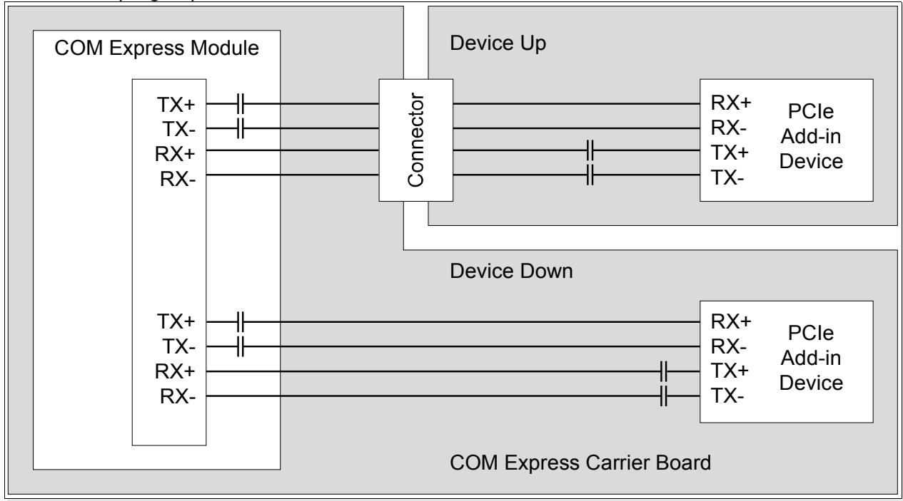
“Device Down” refers to a PCIe target device implemented down on the Carrier Board. “Device Up” refers to a PCIe target device implemented on a slot card (or mini-PCIe card, ExpressCard, AMC card). There are several distinctions between a PCIe “Device Down” and “Device Up” implementation:
# Device Down:
● Coupling caps for the target device PCIe TX lines (COM Ex Module PCIe RX lines) are down on the Carrier Board, close to the target device TX pins;
Trace length allowed for PCIe signals on the Carrier Board is longer for the Device Down case than for Device Up. See Section 6.5.1. 'PCI Express Trace Routing Guidelines' on page 182 for trace length details.
# Device Up:
● Coupling caps for the target device PCIe TX lines (COM Ex Module PCIe RX lines) are up on the slot card.
Trace length allowed for PCIe signals on the Carrier Board is shorter than for the Device Down case, to allow for slot card trace length. See Section 6.5.1 'PCI Express Trace Routing Guidelines' on page 182 for trace length details.
The coupling caps for the Module PCIe TX lines are defined by the COM Express specification to be on the Module.
# 2.3.5. Schematic Examples
# 2.3.5.1. Reference Clock Buffer
The COM Express Specification calls for one copy of the PCIe reference clock pair to be brought out of the Module. This clock is a 100MHz differential pair and is sometimes known as a “hint” clock. The clock allows the PLL in the target PCIe device to lock faster onto the embedded clock in the PCIe bit stream.
If the Carrier Board implements only one PCIe device or slot, then the PCIe reference clock pair from the Module may be routed directly to that device or slot. However, if there are two or more PCIe devices or slots on the Carrier Board, then the Module PCIe reference clock should be buffered. A device which meets the jitter requirements for the intended PCI Express generation must be used.
The IDT9DB233, IDT9DB433, IDT9DB844 have two, four and eight differential output replicas of the input clock, respectively. Each target device (PCIe “device down” chip, slot, Express Card slot, PEG slot) should get an individual copy of the reference clock. Similar parts may be available from other vendors.
The PCIe Clock buffers have both PLL and bypass modes. In some situations it is preferable to operate the clock buffer in bypass mode.
The reference clock pairs should be routed as directly as possible from source to destination.
Figure 6: PCIe Reference Clock Buffer
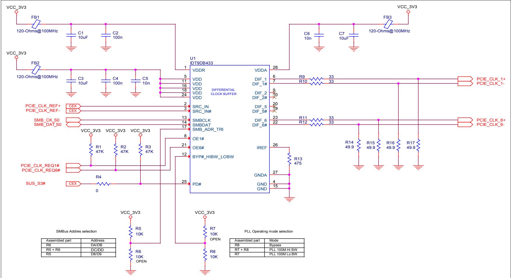
The following notes apply to Figure 6 'PCIe Reference Clock Buffer'.
Nets that tie directly to the COM Express connector are indicated with the CEX flag in the off-page connection symbol.
Each clock pair is routed point to point to each connector or end device using differential signal routing rules.
Each clock output pair in the example shown is terminated close to the IDT9DB433 buffer pins with a series resistor (shown as 33 Ω) and a termination to GND (shown as 49.9 Ω), per the vendor's recommendations. Other vendors may have different recommendations, particularly in regard to the source termination to GND.
SMBUS software can enable or disable clock-buffer outputs. Configuration resistors or alternativly the SMBUS also allow software to put the clock buffer into "Bypass Mode", which experience has shown is needed in some Carrier situations. Please refer to chapter 2.19 'System Management Bus (SMBus)' on page 123 below for more information on SMBUS. Disable unused outputs to reduce emissions.
The CLKREQ0# and CLKREQ1# should be pulled low to enable the corresponding clock buffer outputs. For applications in which power management is not a concern, these inputs may be tied low to permanently enable the outputs.
# 2.3.5.2. Reset
The PCI Interface of the COM Express Type 2 Module shares the reset signal 'PCI\_RESET#' with the PCI Express interface. PCI\_RESET# is not available on all COM Express Module Types. When design a carrier to support Module Types supporting PCI\_RESET#, it is recommended to use PCI\_RESET# to generate PCIE\_RESETn#. If the carrier supports COM Express Module Types without PCI\_RESET#, then it is recommended to use the COM Express signal CB\_RESET# as this signal is available on all COM Express pin-out types. The signal PCIE\_RESETn# in the schematics below is a buffered copy of either the PCI\_RESET# or the CB\_RESET# signal. It is not the same signal as PCI\_RESET#.
# 2.3.5.3. x1 Slot Example
An example of a x1 PCIe slot is shown in Figure 7 below. The source specification for slot implementations is the PCI-SIG PCI Express Card Electromechanical Specification.
Figure 7: PCI Express x1 Slot Example
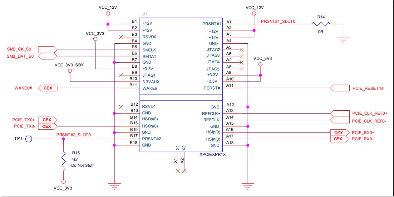
The example above shows COM Express PCIe lane 0 connected to the slot. Other lanes may be used, depending on what is available on the particular Module being used.
No coupling caps are required on the PCIe data or clock lines. The PCIe TX series coupling caps on the data lines are on the COM Express Module. The PCIe RX coupling caps are up on the slot card.
Slot signals REFCLK+ and REFCLK- (pins A13 and A14) are driven by the Clock Buffer, which is shown in Figure 6 'PCIe Reference Clock Buffer' on page 35. If there is only one PCIe target on the Carrier Board, the Clock Buffer may be omitted and the slot REFCLK signals may be driven directly by the COM Express Module.
The slot PERST# signal (pin A11) is driven by a buffered copy of the COM Express PCI\_RESET# signal. A buffered copy of CB\_RESET# could also be used. If the Carrier Board only has one or two target devices, an unbuffered PCI\_RESET# or CB\_RESET# could be used.
The slot signals PRSNT1# and PRSNT2# are part of a mechanism defined in the PCI Express Card Electromechanical Specification to allow hot-plugged PCIe cards. However, most systems do not implement the support circuits needed to complete hot-plug capability. If used, the scheme works as follows: in Figure 7 above, PRSNT1# (pin A1) is pulled low on the Carrier Board through R14. On the slot card, PRSNT1# is routed to PRSNT2# (pin B17). The state of slot pin B17 may be read back by the BIOS or system software, if routed to an input port pin that can be read by software. If a slot card is present, this pin reads back low; if the slot is empty, the pin will be read high. Software then uses this information to apply power to the card. There is no standard input port pin defined by COM Express for this function. For systems that are not trying to implement hot-swap capability, it is not necessary to be able to read back the state of the PRSNT2# pin. Hence it is shown in the figure above as being brought to a test point.
Nets SMB\_CK\_S0 and SMB\_DAT\_S0 are sourced from COM Express Module pins B13 and B14 respectively. \_S0 version of SMBUS needs to be FET isolated from Module version which is on the \_S5 power rail. The SMBUS supports card-management support functions. SMBUS software can save the state of the slot-card device before a Suspend event, report errors, accept control parameters, return status information and card information such as a serial number. Support for the SMBUS is optional on the slot card. Please refer to chapter 2.19 'System Management Bus (SMBus)' on page 123 below for more information on SMBUS.
WAKE0# is asserted by the slot card to cause COM Express Module wake-up at Module pin B66. This is an open-drain signal. It is an input to the Module and is pulled up on the Module. Other WAKE0# sources may pull this line low; it is a shared line.
Slot JTAG pins on A5-A8 are not used.
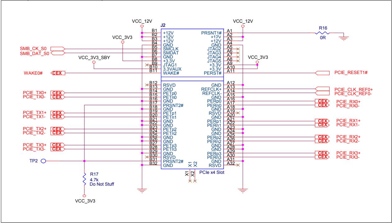
# 2.3.5.4. x4 Slot Example
Figure 8: PCI Express x4 Slot Example
# 2.3.5.5. PCIe x1 Generic Device Down Example
Figure 9: PCI Express x1 Generic Device Down Example
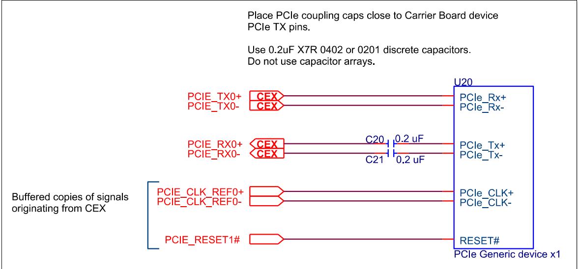
A generic example of a PCIe x1 device on a COM Express Carrier Board is shown in the figure above. Only the signals that interface to the COM Express Module in the full power-on state (S0) are shown here.
If the Carrier Board device is to support power management features, then some additional signals may come into play. To support wake-up from Suspend states, the Carrier Board device may assert the COM Express WAKE0# input by driving it low through an open drain device.
Some power managed Carrier Board PCIe devices may also have a CLKREQ# signal to disable the PCIe reference clock during periods of inactivity. There is no COM Express destination for this line. It may be used with certain clock buffers – see Figure 6 'PCIe Reference Clock Buffer' on page 35.
Carrier Board PCIe devices may also require SMBUS support. If the Carrier Board device has a Suspend power rail and if its SMBUS pins use that rail, then the device's SMBUS pins may be routed directly to the corresponding COM Express SMBUS pins (SMB\_CK, SMB\_DAT and SMB\_ALERT#). If the Carrier Board SMBUS pins are not powered by the Suspend rail, they must be isolated from the COM Express SMBUS lines by isolation FETs or bus switches. Refer to Section 2.19 'System Management Bus (SMBus)' on page 123 for details.
# 2.3.5.6. PCIe x4 Generic Device Down Example
Figure 10: PCI Express x4 Generic Device Down Example
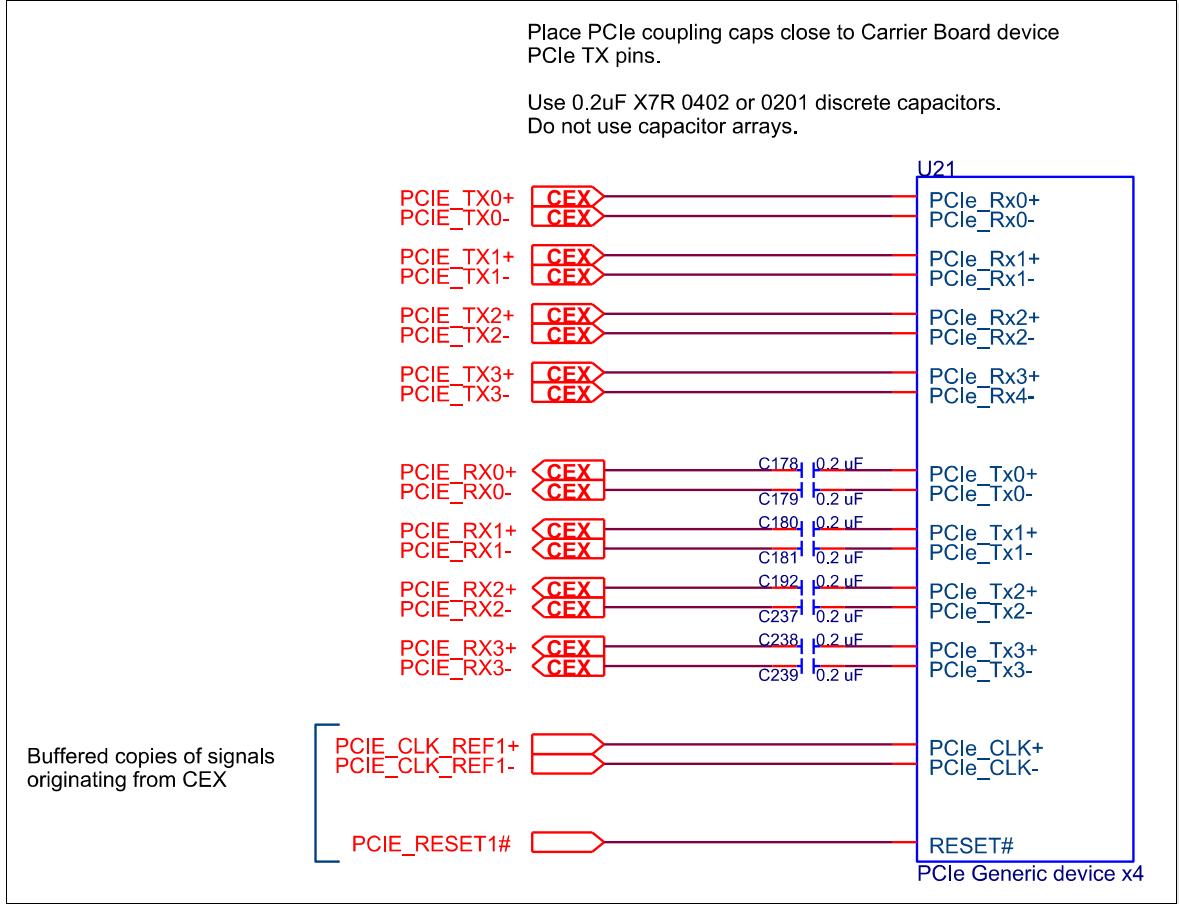
A generic example of a PCIe x4 device on a COM Express Carrier Board is shown in the figure above. Only the signals that interface to the COM Express Module in the full power-on state (S0) are shown here.
If the Carrier Board device is to support power management features, then some additional signals may come into play. To support wake-up from Suspend states, the Carrier Board device may assert the COM Express WAKE0# input by driving it low through an open drain device.
Some power managed Carrier Board PCIe devices may also have a CLKREQ# signal to disable the PCIe reference clock during periods of inactivity. There is no COM Express destination for this line. It may be used with certain clock buffers – see Figure 6 'PCIe Reference Clock Buffer' on page 35 above.
Carrier Board PCIe devices may also require SMBUS support. If the Carrier Board device has a Suspend power rail and if its SMBUS pins use that rail, then the device's SMBUS pins may be routed directly to the corresponding COM Express SMBUS pins (SMB\_CK, SMB\_DAT and SMB\_ALERT#). If the Carrier Board SMBUS pins are not powered by the Suspend rail, they must be isolated from the COM Express SMBUS lines by isolation FETs or bus switches. Refer to Section 2.19 'System Management Bus (SMBus)' on page 123 for details.
# 2.3.5.7. PCI Express Mini Card
The PCI Express Mini Card is a small form factor add-in card optimized for mobile computing and embedded platforms. It is not hot-swappable (for hot swap capability, use an ExpressCard interface, described in Section 2.3.5.8. 'ExpressCard' on page 44 below).
PCI Express Mini Cards are popular for implementing features such as wireless LAN. A small footprint connector can be implemented on the Carrier Board providing the ability to insert different removable PCI Express Mini Cards. Using this approach gives the flexibility to mount an upgradeable, standardized PCI Express Mini Card device to the Carrier Board without additional expenditure of a redesign.
A PCI Express Mini Card interface includes a single x1 PCIe link and a single USB 2.0 channel. The mini PCI Express Card host should offer both interfaces. The PCI Express Mini Card installed into the socket may use either interface.
The source specification for mini-PCI Express Cards is the PCI Express Mini Card Electromechanical Specification.
Two different card sizes of PCI Express Mini Card are allowed: a full sized card with 30.00 mm x 50.95 mm and a half sized card with 30.00 mm x 26.80 mm.
Figure 11: PCI Express Mini Full Sized Card Footprint
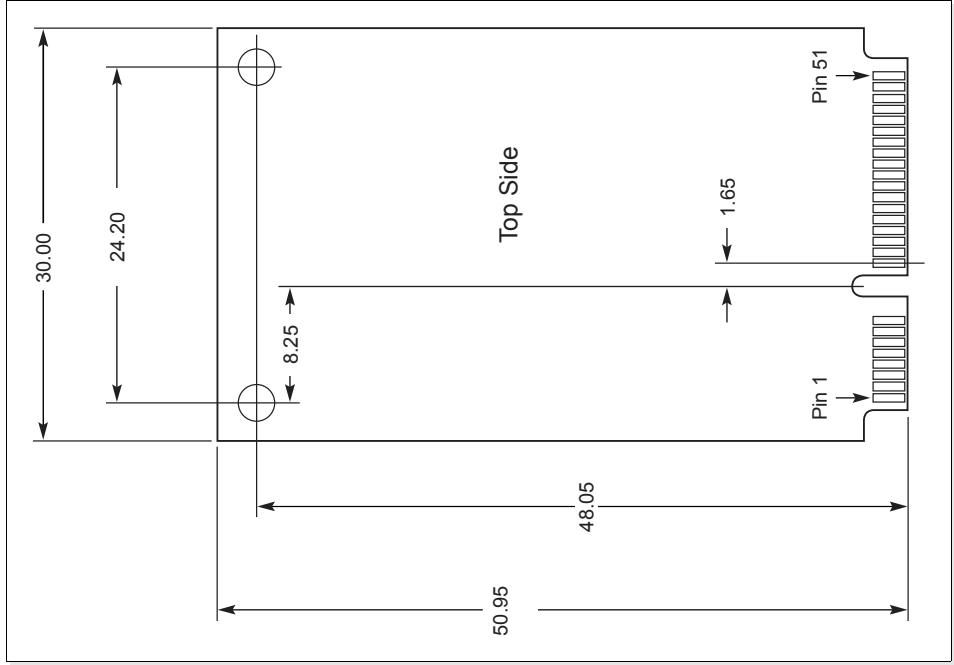
Figure 12: PCI Express Mini Card Connector
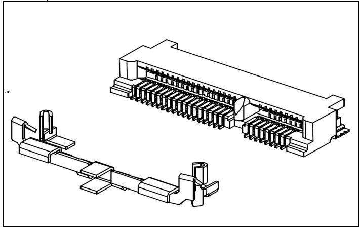
A typical PCI Express Mini-Card socket is shown in Figure 12 above.
The pins used on a PCI Express Mini-Card socket are listed in Table 7: PCIe Mini Card Connector Pin-out below.
Figure 13: PCI Express Mini Card Connector on COM Express Carrier Board
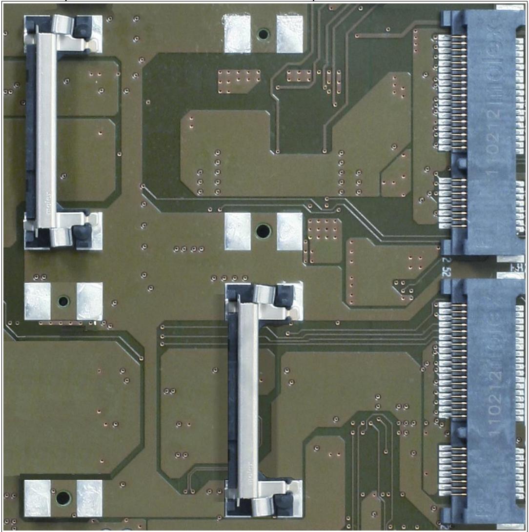
The different card sized can be easily handled on the Carrier Board by having the latches optionally placed on the full size position or on the half size position as shown in Figure 13 above.
Table 7: PCIe Mini Card Connector Pin-out
| Pin | Signal | Description | Pin | Signal | Description |
| 1 | WAKE# | Requests the host interface to return to full operation and respond to PCIe. | 2 | +3.3VAux | Auxiliary voltage source, 3.3V. |
| 3 | COEX1 | Coexistence Pin 1 | 4 | GND | Ground |
| 5 | COEX2 | Coexistence Pin 2 | 6 | +1.5V | Secondary voltage source, 1.5V. |
| 7 | CLKREQ# | Reference clock request signal. | 8 | UIM_PWR | Power source for User Identity Modules (UIM). |
| 9 | GND | Ground | 10 | UIM_DATA | Data signal for UIM. |
| 11 | REFCLK- | Reference Clock differential pair negative signal. | 12 | UIM_CLK | Clock signal for UIM. |
| 13 | REFCLK+ | Reference Clock differential pair positive signal. | 14 | UIM_RESET | Reset signal for UIM. |
| 15 | GND | Ground | 16 | UIM_SPU | Standard or Proprietary Use signal for UIM. |
Mechanical Key
| 17 | UIM_IC_DM | Inter-Chip USB D- Data line | 18 | GND | Ground |
| 19 | UIM_IC_DP | Inter-Chip USB D+ Data line | 20 | W_DISABLE1# | Wireless Disable Signal 1 |
| 21 | GND | Ground | 22 | PERST# | PCI Express Reset |
| 23 | PERn0 | Receiver differential pair negative signal, Lane 0. | 24 | +3.3Vaux | Auxiliary voltage source, 3.3V. |
| 25 | PERp0 | Receiver differential pair positive signal, Lane 0. | 26 | GND | Ground |
| 27 | GND | Ground | 28 | +1.5V | Secondary voltage source, 1.5V. |
| 29 | GND | Ground | 30 | SMB_CLK | System Management Bus Clock. |
| 31 | PETn0 | Transmitter differential pair negative signal, Lane 0. | 32 | SMB_DATA | System Management Bus Data. |
| 33 | PETp0 | Transmitter differential pair positive Signal, Lane 0. | 34 | GND | Ground |
| 35 | GND | Ground | 36 | USB_D- | USB Serial Data Interface differential pair, negative signal. |
| 37 | GND | Ground | 38 | USB_D+ | USB Serial Data Interface differential pair, positive signal. |
| 39 | +3.3Vaux | Auxiliary voltage source, 3.3V. | 40 | GND | Ground |
| 41 | +3.3Vaux | Auxiliary voltage source, 3.3V. | 42 | LED_WWAN# | LED status indicator signals provided by the system. |
| 43 | GND | Ground | 44 | LED_WLAN# | LED status indicator signals provided by the system. |
| 45 | RSVD | Reserved | 46 | LED_WPAN# | LED status indicator signals provided by the system. |
| 47 | RSVD | Reserved | 48 | +1.5V | Secondary voltage source, 1.5V. |
| 49 | RSVD | Reserved | 50 | GND | Ground |
| 51 | W_DISABLE2# | Wireless Disable Signal 2 | 52 | +3.3V | Primary voltage source, 3.3V. |
Figure 14: PCIe Mini Card Reference Circuitry
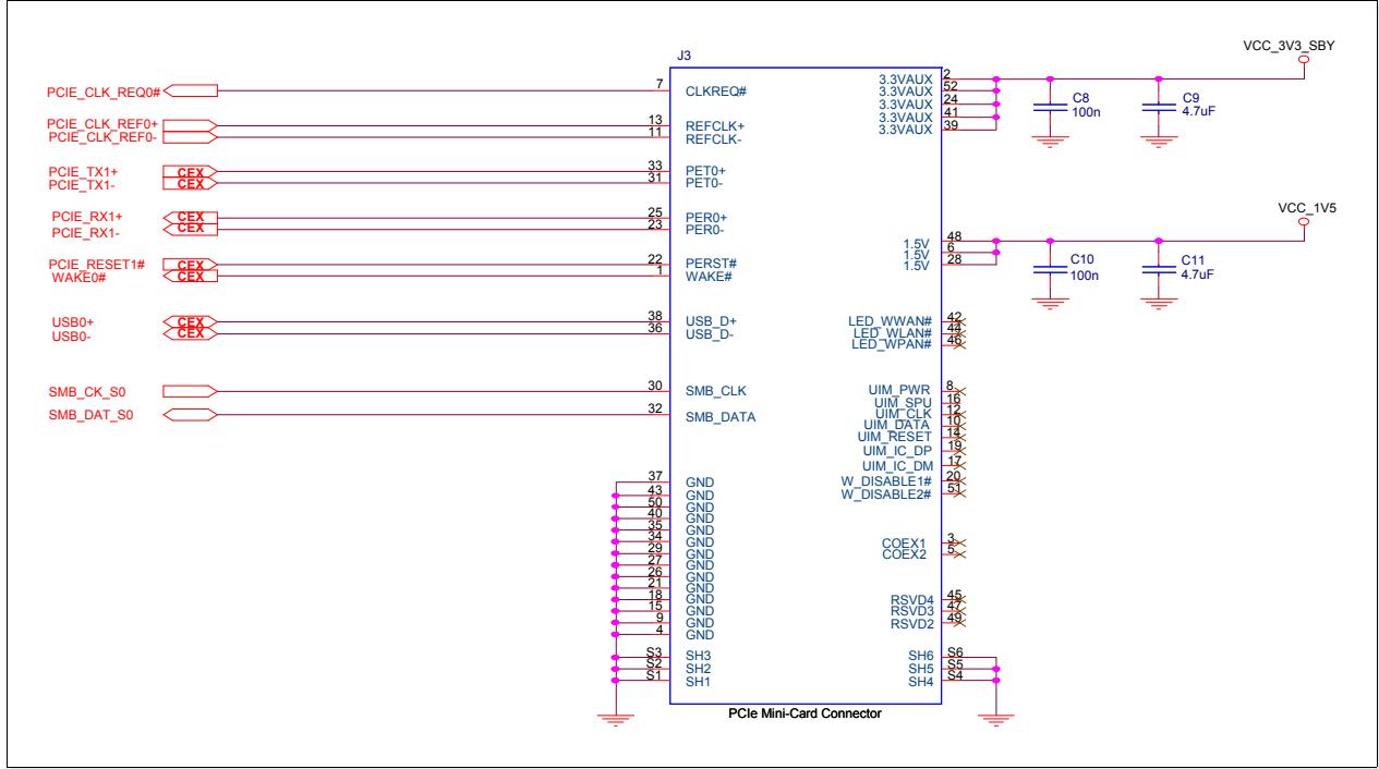
A PCI Express Mini Card schematic example is shown in Figure 14 above. The reference clock pair is sourced from the zero delay clock buffer shown earlier in Figure 6 'PCIe Reference Clock Buffer' on page 35 above. The clock pair is enabled when the PCI Express Mini-Card pulls its CLKREQ# pin low.
The example shows COM Express PCIe lane 1 and USB port 0 used, but other assignments may be made depending on Module capabilities and the system configuration.
If Suspend mode operation is not required, then the 3.3VAUX pin may be tied to VCC\_3V3. The WAKE# pin should be left open in this case.
# 2.3.5.8. ExpressCard
ExpressCards are small form factor hot-swappable peripheral cards designed primarily for mobile computing. The card’s electrical interface is through either a x1 PCIe link or a USB 2.0 link. Per the ExpressCard source specification, the host interface should support both the PCIe and USB links. The ExpressCard device may utilize one or the other or both interfaces.
There are several form factors defined, including: 34mm x 75mm; 54mm x 75mm; 34mm x 100mm, and 54mm x 100mm. All of the form factors use the same electrical and physical socket interface.
ExpressCards are the successor to Card Bus Cards (which are PCI-based). Card Bus cards, in turn, are the successors to PCMCIA cards. All three formats are defined by the PCMCIA Consortium.
The source specification document for ExpressCards is the ExpressCard Standard.
COM Express includes four signals that are designated for the support of two ExpressCard slots:
Table 8: Support Signals for ExpressCard
| Signal | Pin | Description | I/O |
| EXCD0_CPPE# | A49 | ExpressCard capable card request, slot 0. | I 3.3V CMOS |
| EXCD1_CPPE# | B48 | ExpressCard capable card request, slot 1. | I 3.3V CMOS |
| EXCD0_PERST# | A48 | ExpressCard reset, slot 0. | O 3.3V CMOS |
| EXCD1_PERST# | B47 | ExpressCard reset, slot 1. | O 3.3V CMOS |
Figure 15: ExpressCard Size
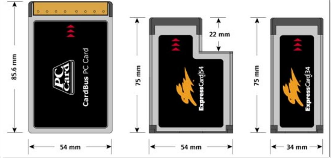
Figure 16: ExpressCard Sockets
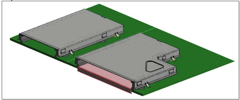
Figure 17: PCI Express: ExpressCard Example
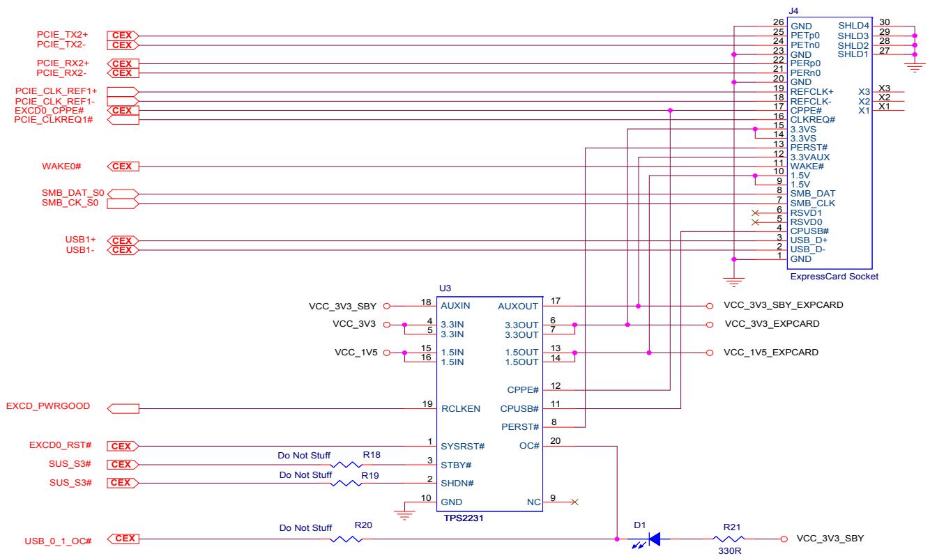
Bypass caps for TPS2231
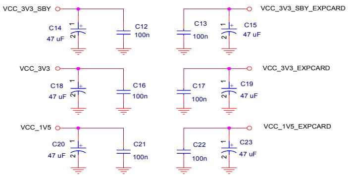
Figure 17 above shows an ExpressCard implementation. The example shows COM Express PCIe lane 2 and USB port 1 used, but other assignments may be made depending on Module capabilities and the system configuration.
Nets PCIE\_TX2+ and PCIE\_TX2- are sourced from the COM Express Module. These lines drive the PCIe receivers on the Express Card. No coupling capacitors are required on the Carrier Board. These lines are capacitively coupled on the COM Express Module.
Nets PCIE\_RX2+ and PCIE\_RX2- are driven by the Express Card. No coupling capacitors are required on the Carrier Board. These lines are capacitively coupled on the Express Card.
Nets PCIE\_REF\_CLK1+ and PCIE\_REF\_CLK1- are sourced from the PCIe Reference Clock Buffer (described earlier in Section 2.3.5.1. 'Reference Clock Buffer' on page 34 above).
CPPE# is pulled low on the Express Card to indicate that a card is present and has a PCIe interface. CPUSB# is pulled low on the Express Card to indicate the presences of an Express Card and a USB 2.0 interface. Either CPPE# or CPUSB# low causes the TPS2231 ExpressCard power control IC to provide power to the Express Card.
The TPS2231 includes a number of integrated pull-up resistors. Other solutions may require external pull-ups not shown in this schematic example.
CLKREQ# is used for dynamic-clock management. When the signal is pulled low, the dynamicclock management feature is not supported.
The ExpressCard PCIe reset signal, PERST#, is driven by the TPS2231. PERST# is asserted if the power rails are out of spec or if the COM Express ExpressCard reset, EXCD0\_PERST#, is asserted.
WAKE# is asserted by the Express Card to cause the COM Express Module to wake-up at COM Express Module pin B66 WAKE0#. WAKE0# is pulled up on the Module to facilitate the “wire-ORed” interconnect from other WAKE0# sources.
SMB\_CK and SMB\_DAT are sourced from COM Express Module pins B13 and B14 respectively. The SMBUS supports client-alerting, wireless RF management, and sideband management. Support for the SMBUS is optional on the Carrier Board and the Express Card.
# 2.3.6. PCI Express Routing Considerations
New Carrier designs should route the PCIe lanes with 85Ω (+/- 15%) differential impedance. Previous designs that supported Gen1 and Gen2 signaling used 92Ω (+/- 10%) differential impedance. Gen1 only designs used 100Ω (+/- 20%) differential impedance. Newer designs should use 85Ω (+/- 15%) differential impedance to support Gen1, Gen2 and Gen3 signaling. Route the traces as differential pairs, preferably referenced to a continuous GND plane with a minimum of via transitions.
PCIe pairs need to be length-matched within a given pair (“intra-pair”), but the different pairs do not need to be closely matched (“inter-pair”).
PCB design rules for these signals are summarized in Section 6. 'Carrier Board PCB Layout Guidelines' on page 173.
# 2.3.6.1. Polarity Inversion
Per the PCI Express Card Electromechanical Specification, all PCIe devices must support polarity inversion on each PCIe lane, independently of the other lanes. This means that, for example, you can route the Module PCIE\_TX0+ signal to the corresponding ‘-’ pin on the slot or target device, and the PCIE\_TX0- signal to the corresponding ‘+’ pin. If this makes the layout cleaner, with fewer layer transitions and better differential pairs, then take advantage of this PCIe feature.
# 2.3.6.2. Lane Reversal
PCIe lane reversal is not supported on the COM Express general purpose PCIe lanes. For x1 links, lane reversal is not relevant. It would potentially be useful for a x4 link, but is not supported in the COM Express specification. It is also not supported by the current crop of South Bridge chip-set components commonly used to create the general purpose PCIe lanes on COM Express Modules.
Lane reversal is supported for the COM Express x16 PEG interface. See Section 2.4. 'PEG (PCI Express Graphics)' on page 48 for details.
# 2.4. PEG (PCI Express Graphics)
# 2.4.1. Signal Definitions
The PEG Port can utilize COM Express PCIe lanes 16-31 and is suitable to drive a link for an external high-performance PCI Express Graphics card, if implemented on the COM Express Module. Graphics Cards implemented as x16 use COM Express PCIe lanes 16-31; Graphics Cards implemented as x8 lanes should use COM Express PCIe lanes 16-23. Each lane of the PEG Port consists of a receive and transmit differential signal pair designated 'PEG\_RX0' (+ and -) to 'PEG\_RX15' (+ and -) and correspondingly from 'PEG\_TX0' (+ and -) to 'PEG\_TX15' (+ and -). The corresponding signals can be found on the Module connector rows C and D.
On Type 2 Modules the pins of the PEG Port might be shared with other functionality like SDVO or DVO, depending on the chipset used. SDVO and PEG are defined on COM Express specification for Type 2 Modules as “may be used”. Please be sure the functionality you require is supported by your Module vendor.
Table 9: PEG Signal Description
| Signal | Pin# | Description | I/O | Comment |
| PEG_RX0+PEG_RX0- | C52C53 | PEG channel 0,Receive Input differential pair. | I PCIE | Type 2 Shared with: | SDVO_TVCLKIN+ SDVO_TVCLKIN- |
| PEG_TX0+PEG_TX0- | D52D53 | PEG channel 0, Transmit Output differential pair. | O PCIE | Type 2 Shared with: | SDVOB_RED+ SDVOB_RED- |
| PEG_RX1+PEG_RX1- | C55C56 | PEG channel 1,Receive Input differential pair. | I PCIE | Type 2 Shared with: | SDVOB_INT+ SDVOB_INT- |
| PEG_TX1+PEG_TX1- | D55D56 | PEG channel 1, Transmit Output differential pair. | O PCIE | Type 2 Shared with: | SDVOB_GRN+ SDVOB_GRN- |
| PEG_RX2+PEG_RX2- | C58C59 | PEG channel 2,Receive Input differential pair. | I PCIE | Type 2 Shared with: | SDVO_FLDSTALL+ SDVO_FLDSTALL- |
| PEG_TX2+PEG_TX2- | D58D59 | PEG channel 2, Transmit Output differential pair. | O PCIE | Type 2 Shared with: | SDVOB_BLU+ SDVOB_BLU- |
| PEG_RX3+PEG_RX3- | C61C62 | PEG channel 3,Receive Input differential pair. | I PCIE | | |
| PEG_TX3+PEG_TX3- | D61D62 | PEG channel 3, Transmit Output differential pair. | O PCIE | Type 2 Shared with: | SDVOB_CK+ SDVOB_CK- |
| PEG_RX4+PEG_RX4- | C65C66 | PEG channel 4,Receive Input differential pair. | I PCIE | | |
| PEG_TX4+PEG_TX4- | D65D66 | PEG channel 4, Transmit Output differential pair. | O PCIE | Type 2 Shared with: | SDVOC_RED+ SDVOC_RED- |
| PEG_RX5+PEG_RX5- | C68C69 | PEG channel 5,Receive Input differential pair. | I PCIE | Type 2 Shared with: | SDVOC_INT+ SDVOC_INT- |
| PEG_TX5+PEG_TX5- | D68D69 | PEG channel 5, Transmit Output differential pair. | O PCIE | Type 2 Shared with: | SDVOC_GRN+ SDVOC_GRN- |
| PEG_RX6+PEG_RX6- | C71C72 | PEG channel 6,Receive Input differential pair. | I PCIE | | |
| PEG_TX6+PEG_TX6- | D71D72 | PEG channel 6, Transmit Output differential pair. | O PCIE | Type 2 Shared with | SDVOC_BLU+ SDVOC_BLU- |
| PEG_RX7+PEG_RX7- | C74C75 | PEG channel 7,Receive Input differential pair. | I PCIE | | |
| PEG_TX7+PEG_TX7- | D74D75 | PEG channel 7, Transmit Output differential pair. | O PCIE | Type 2 : Shared with | SDVOC_CK+ SDVOC_CK- |
| PEG_RX8+PEG_RX8- | C78C79 | PEG channel 8,Receive Input differential pair. | I PCIE | | |
| PEG_TX8+PEG_TX8- | D78D79 | PEG channel 8, Transmit Output differential pair. | O PCIE | | |
| PEG_RX9+PEG_RX9- | C81C82 | PEG channel 9,Receive Input differential pair. | I PCIE | | |
| Signal | Pin# | Description | I/O | Comment |
| PEG_TX9+PEG_TX9- | D81D82 | PEG channel 9, Transmit Output differential pair. | O PCIE | |
| PEG_RX10+PEG_RX10- | C85C86 | PEG channel 10, Receive Input differential pair. | I PCIE | |
| PEG_TX10+PEG_TX10- | D85D86 | PEG channel 10, Transmit Output differential pair. | O PCIE | |
| PEG_RX11+PEG_RX11- | C88C89 | PEG channel 11, Receive Input differential pair. | I PCIE | |
| PEG_TX11+PEG_TX11- | D88D89 | PEG channel 11, Transmit Output differential pair. | O PCIE | |
| PEG_RX12+PEG_RX12- | C91C92 | PEG channel 12, Receive Input differential pair. | I PCIE | |
| PEG_TX12+PEG_TX12- | D91D92 | PEG channel 12, Transmit Output differential pair. | O PCIE | |
| PEG_RX13+PEG_RX13- | C94C95 | PEG channel 13, Receive Input differential pair. | I PCIE | |
| PEG_TX13+PEG_TX13- | D94D95 | PEG channel 13 Transmit Output differential pair. | O PCIE | |
| PEG_RX14+PEG_RX14- | C98C99 | PEG channel 14, Receive Input differential pair. | I PCIE | |
| PEG_TX14+PEG_TX14- | D98D99 | PEG channel 14, Transmit Output differential pair. | O PCIE | |
| PEG_RX15+PEG_RX15- | C101C102 | PEG channel 15, Receive Input differential pair. | I PCIE | |
| PEG_TX15+PEG_TX15- | D101D102 | PEG channel 15, Transmit Output differential pair. | O PCIE | |
| SDVO_I2C_CLK | D73 | I2C based control signal (clock) for SDVO device. | O 2.5V CMOS | SDVO enabled if this line is pulled up to 2.5V on Carrier or on ADD2 (Type 2 only) |
| SDVO_I2C_DATA | C73 | I2C based control signal (data) for SDVO device | I/O 2.5V OD CMOS | SDVO enabled if this line is pulled up to 2.5V on Carrier or on ADD2 (Type 2 only) |
| PEG_LANE_RV# | D54 | PCI Express Graphics lane reversal input strap. Pull low on the carrier board to reverse lane order. | I 3.3V CMOS | |
| PEG_ENABLE# | D97 | PEG enable function. Strap to enable PCI Express x16 external graphics interface. Pull low to disable internal graphics and enable the x16 interface. | I 3.3V CMOS | Type 2 only |
| PCIE_CLK_REF+PCIE_CLK_REF- | A88A89 | PCIe Reference Clock for all COM Express PCIe lanes, and for PEG lanes | O CMOS | COM Express only allocates a single reference clock |
# 2.4.2. PEG Configuration
The COM Express PCIe Graphics (PEG) Port is comprised of COM Express PCIe lanes 16-31. The primary use of this set of signals is to interface to off-Module graphics controllers or cards. The COM Express spec also allows these pins to be shared with a set of Module generated SDVO lines.
If the PEG interface is not used for an external graphics card or SDVO, it may be possible to use these PCIe lanes for other Carrier Board PCIe devices. The details of this usage are Module and Module chip-set dependent. Operation in a x1 link is also supported. Wider links (x2, x4, x8, x16) are chip-set dependent. Refer to the Module product documentation for details.
The COM Express specification defines a fill order for this set of PCIe lanes. Larger link widths go to the lower lanes. Refer to the COM Express specification for details.
# 2.4.2.1. Using PEG Pins for an External Graphics Card
To use the COM Express PEG lanes for an external graphics device or card, the Type 2 Module's PEG\_ENABLE# line (pin D97 on the Module C-D connector) must be pulled low. Pulling this pin low disables the Module's internal graphics controller and makes the PEG x16 interface available to an external controller.
The usual effect of pulling PEG\_ENABLE# low is to disable the on-Module graphics engine. For some Modules, it is possible to configure the Module such that the internal graphics engine remains active, even when the external PEG interface is being used for a Carrier Board graphics device. This is Module dependent. Check with your vendor.
If the external graphics controller is “down” on the Carrier Board, then the PEG\_ENABLE# line should be pulled to GND on the Carrier Board.
There are four copies of PRSNT2# defined for slot cards, to allow detection of x1, x4, x8 and x16 cards. For PEG slot use, the PRSNT2# signals for the x1 and x4 links are used for SDVO detection per the following chart.
To enable carrier flexibility in slot configuration and to support x1, x4, x8 and x16 PCI Express cards as well as ADD2/MEC cards and MEC cards that utilize both SDVO and x1 PCI Express, a jumper is recommended on the carrier to configure the PEG\_ENABLE# signal. For carrier implementations only requiring support of x8 and x16 PCI Express graphics cards and SDVO ADD2 cards, the PRSNT2# signals on slot pins B48 and B81 may be tied to COM Express Module PEG\_ENABLE# pin D97 to automatically configure the Module based on the card inserted.
Table 10: PEG Configuration Pins
| Slot Signal | Slot Pin | Carrier Board Connection | COM Ex Pin | Comment |
| PRSNT1# | A1 | Tie to GND through low value resistor | | Pins A1, B48 and B81 are tied together on a PEG slot card. Not tied together on ADD2. |
| PRSNT2# | B17 | To COM Ex SDVO_I2C_CLK line | D73 | SDVO use – pulled to 2.5V on ADD2 |
| PRSNT2# | B31 | To COM Ex SDVO_I2C_DAT line | C73 | SDVO use – pulled to 2.5V on ADD2 |
| PRSNT2# | B48 | Not connected | | |
| PRSNT2# | B81 | To COM Ex PEG_ENABLE# | | |
# 2.4.2.2. Using PEG Pins for SDVO (Type 2 Modules only)
The COM Express Module graphics controller configures the PEG lines for SDVO operation if it detects that COM Express signals SDVO\_I2C\_CLK and SDVO\_I2C\_DATA are pulled high to 2.5V, and if the PEG\_ENABLE# line is left floating. This combination leaves the Module's internal graphics engine enabled but converts the output format to SDVO. The SDVO\_I2C\_CLK and SDVO\_I2C\_DATA lines are pulled to 2.5V on an ADD2 card.
For a device “down” SDVO converter, the SDVO\_I2C\_CLK and SDVO\_I2C\_DATA lines have to be pulled up to 2.5V on the Carrier Board.
# 2.4.2.3. Using PEG Pins for General Purpose PCIe Lanes
The COM Express PEG lanes may be used for general-purpose use if the PEG port is not being used as an interface to an external graphics device. The characteristics of this usage are Module and chip-set dependent.
Modules that employ desktop and mobile chip-sets with PEG capability can usually be set up to allow the COM Express PEG lanes to be configured as a single general purpose PCIe link, with link width possibilities of x1, x4, x8 or x16. The x1 configuration should always work; the wider links may be Module and chip-set dependent. Check with your vendor.
Modules based on server-class chip-sets may allow multiple links over the PEG lanes – for example, a x8 link on COM Express PCIe lanes 16 through 23 and a x4 link over lanes 24 through 27. This is Module and chip-set dependent.
PEG\_ENABLE# should be left open when the PEG lanes are to be used for general purpose PCIe links.
# 2.4.3. Reference Schematics
# 2.4.3.1. x1, x4, x8, x16 Slot
Figure 18 below illustrates the pin-out definition for the standard x1, x4, x8 and x16 PCI Express connectors. The lines in the diagram depict where each different connector type ends.
Figure 18: x1, x4, x8, x16 Slot
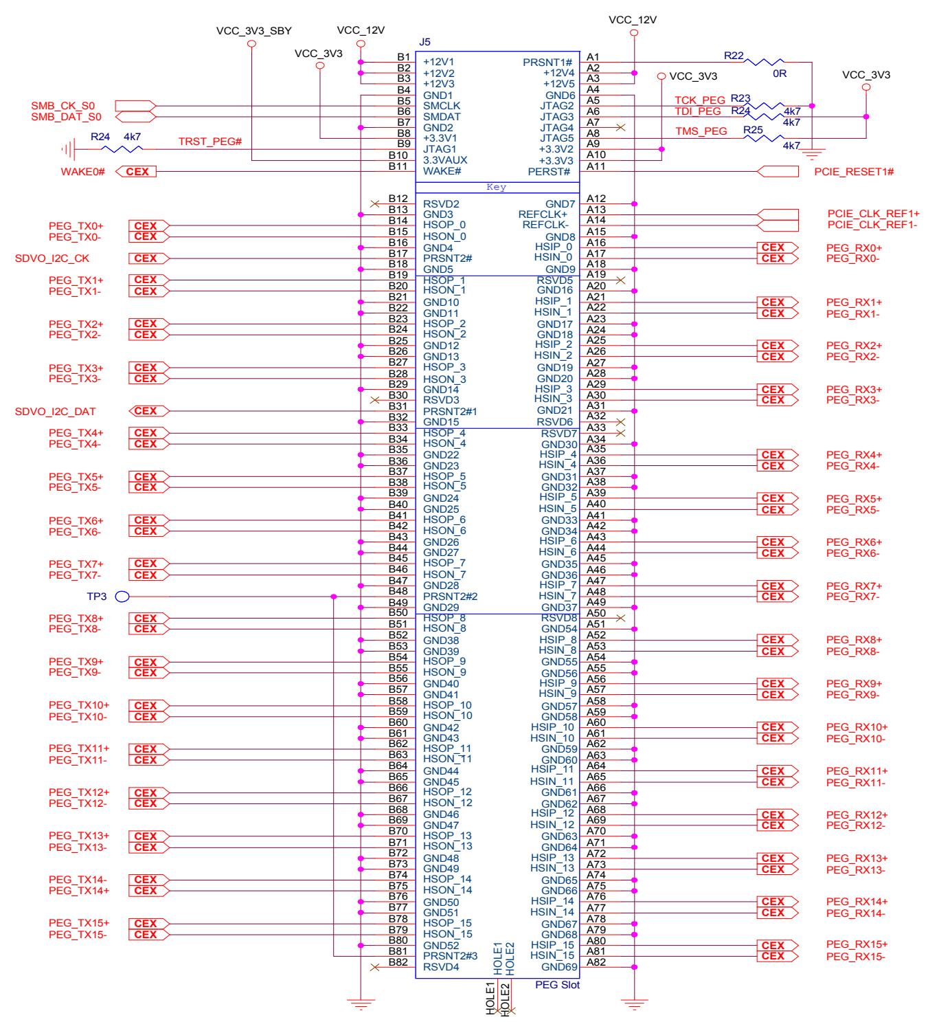
The x16 connector usually is used to drive the PCI Express Graphics Port (PEG) consisting of 16 PEG lanes, which are connected to the appropriate x16 connector pins. For more information about the signal definition of the PEG port, refer to Section 2.4. 'PEG (PCI Express Graphics)' on page 48 above.
# Note: Auxiliary signals
The auxiliary signals are provided on the PCI Express connectors to assist with certain system level functionality or implementations. Some of these signals are required when implementing a PCI connector on the Carrier Board. For more information about this subject, refer to the PCI Express Card Electromechanical Specification, Rev. 1.1 Section 2.
# 2.4.4. Routing Considerations
Please refer to Section 2.3.6 'PCI Express Routing Considerations' on page 47 above.
# 2.4.4.1. Polarity Inversion
Per definition, PCI Express supports polarity inversion by each receiver on a link. The receiver accomplishes this by simply inverting the received data on the differential pair if it detects a polarity inversion during the initial training sequence of the link. In other words, a lane will still work correctly if a positive signal 'PEG\_TX+' from a transmitter is connected to the negative signal 'PEG\_RX-' of the receiver. Vice versa, the negative signal from the transmitter 'PEG\_TX-' must be connected to the positive signal of the receiver 'PEG\_RX+'. This feature can be very useful to make PCB layouts cleaner and easier to route.
Polarity inversion does not imply direction inversion, this means the 'PEG\_TX' differential pairs of the Module must still be connected to the 'PEG\_RX' differential signal pairs of the device.
# 2.4.4.2. Lane Reversal
During the PCB layout of a COM Express Carrier Board, it is quite possible that the signals between the Modules connectors and the PCI Express device on the Carrier Board have to be crossed. To help layout designers overcome this signal crossing scenario, PCI Express specifies Lane Reversal. Lane Reversal is the reverse mapping of lanes for x2 or greater links.
For example, on a link with a width of x16, which supports Lane Reversal, the TX0, TX1, . TX14, TX15 of the transmitting device have to be connected to RX15, RX14, ... RX1, RX0 of the receiving device, and vice versa. See Figure 19 below.
Connectivity before Lane Reversal
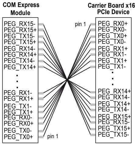
Connectivity after Lane Reversal
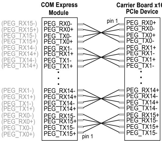
Figure 19: PEG Lane Reversal Mode
To activate the Lane Reversal mode for the PEG Port, the COM Express specification defines an active low signal 'PEG\_LANE\_RV#', which can be found on the Modules connector at row D pin D54. This pin is strapped low on the Carrier Board to invoke Lane Reversal mode.
Note Please be aware that the SDVO lines on Type 2 Modules (Section 2.5.2) that share the PEG Port (Section 2.4) may not support Lane Reversal mode. This is the reason that there are “normal” (ADD2-N) and “reverse” (ADD2-R) pin-out ADD2 cards on the market. ADD2-N cards are used in a PEG slot that does not employ lane reversal. An ADD2-R card is used in a PEG slot that does employ lane reversal.
Check with your Module vendor to see if SDVO Lane Reversal is supported.
# 2.5. Digital Display Interfaces
Module Types 6 and 10 use Digital Display Interfaces (DDI) to provide DisplayPort, HDMI/DVI, and SDVO interfaces. Type 10 Modules can contain a single DDI (DDI[0]) that can support DisplayPort, HDMI/DVI, and SDVO. Type 6 Modules can contain up to 3 DDIs (DDI[1:3]) of which DDI[1:3] can support DisplayPort, HDMI/DVI and DDI[1] can support DisplayPort, HDMI/DVI, and SDVO. The main difference is that SDVO is only supported on DDI[0] for Type 10 Modules and DDI[1] for Type 6 Modules.
Module Type 2 offers additionally the possibility to have SDVO shared with PEG.
# 2.5.1. DisplayPort / HDMI / DVI
DisplayPort was developed by the Video Electronics Standard Association (VESA) in order to create a new digital display port interface to connect a video source to a display device.
DisplayPort can be used to transfer audio and video at the same time, but each one is optional and can be transmitted without the other. A bi-directional, half-duplex auxiliary channel carries device management and device control data for the Main Link, such as VESA EDID.
DisplayPort is nowadays on almost all COM Express Modules available as Dual-mode DisplayPort, that can directly emit single-link HDMI and DVI signals using an adapter, which contains a level shifter to adjust for the lower voltages required by DisplayPort. These adapters can be directly implemented on the Carrier Board to have an easy, simple and future proof implementation of HDMI and/or DVI or an inexpensive cable adapter can be directly connected on the Carrier Board's DisplayPort connector.
# 2.5.1.1. Signal Definitions
Type 10 offers up to one DisplayPort interface and Type 6 Modules up to 3 DisplayPort interfaces. Both implementations are very similar, so only one reference schematic is necessary to show Carrier Board implementation.
Each DisplayPort interface consists of 4 differential lanes, 1 auxiliary lane and 1 hot-plug-detect signal. The DDC\_AUX\_SEL pin should be routed to pin 13 of the DisplayPort connector, to enable Dual-Mode. When HDMI/DVI is directly done on the Carrier Board, this pin shall be pulled to 3.3V with a 100k Ohm resistor to configure the AUX pairs as DDC channels.
Table 11: Display Port / HDMI / DVI Pin-out of Type 10 and Type 6
| COM Express Pin Name | DDI0 Type 10 | DDI1 Type 6 | DDI2 Type 6 | DDI3 Type 6 | Function (DDIX) DisplayPort | Function (DDIX) HDMI / DVI |
| DDIX_PAIR0+ | B71 | D26 | D39 | C39 | DPX_LANE0+ | TMDSX_DATA2+ |
| DDIX_PAIR0- | B72 | D27 | D40 | C40 | DPX_LANE0- | TMDSX_DATA2- |
| DDIX_PAIR1+ | B73 | D29 | D42 | C42 | DPX_LANE1+ | TMDSX_DATA1+ |
| DDIX_PAIR1- | B74 | D30 | D43 | C43 | DPX_LANE1- | TMDSX_DATA1- |
| DDIX_PAIR2+ | B75 | D32 | D46 | C46 | DPX_LANE2+ | TMDSX_DATA0+ |
| DDIX_PAIR2- | B76 | D33 | D47 | C47 | DPX_LANE2- | TMDSX_DATA0- |
| DDIX_PAIR3+ | B81 | D36 | D49 | C49 | DPX_LANE3+ | TMDSX_CLK+ |
| DDIX_PAIR3- | B82 | D37 | D50 | C50 | DPX_LANE3- | TMDSX_CLK- |
| DDIX_HPD | B89 | C24 | D44 | C44 | DPX_HPD | HDMIX_HPD |
| DDIX_CTRLCLK_AUX+ | B98 | D15 | C32 | C36 | DPX_AUX+ | HDMIX_CTRLCLK |
| DDIX_CTRLDATA_AUX- | B99 | D16 | C33 | C37 | DPX_AUX- | HDMIX_CTRLDATA |
| DDIX_DDC_AUX_SEL | B95 | D34 | C34 | C38 | | |
Note: Please verify in the Module's specification if DisplayPort or Dual-Mode DisplayPort is supported.
# 2.5.1.2. Reference Schematic
# DisplayPort Example
Figure 20: DisplayPort Reference Schematics
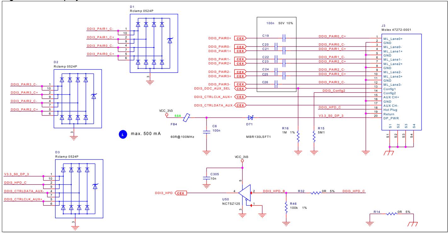
DisplayPort is directly supported by a dual-source DDI. ESD protection, DC blocking capacitors and hot plug detect are the only components required.
The DisplayPort differential data pairs (Lane [0..3]) are AC coupled off Module with capacitors C19-C26. Place the AC blocking capacitors close to the DisplayPort connector. The Aux differential pair is AC coupled on the Module. ESD clamping diodes D1, D2 and D3 protect the Module from external ESD events and should be placed near the DisplayPort connector. The pin-out of the ESD clamp diodes allows for a trace to run under the chip connector to two pins.
The Carrier provides up to 500 mA of 3.3V power to the DisplayPort connector. Diode D71 prevents back feeding of power in the event that the monitor is powered up when the Carrier is powered down.
Config lines 1 and 2 are pulled to ground per the VESA specification.
The DisplayPort Hot Plug Detect signal is buffered by U50 which prevents back feeding of power from the display to the Module as well as level translation to 3.3V levels.
R14 connect logic and chassis ground together. Other techniques may be used depending on the overall grounding strategy.
Note: The reference schematics assume that the Module’s DDI ports are dual-source capable – dual source indicates that the Module can output DisplayPort or HDMI/DVI based on the DDC\_AUX\_SEL signal.
# HDMI Example
Figure 21: HDMI Example
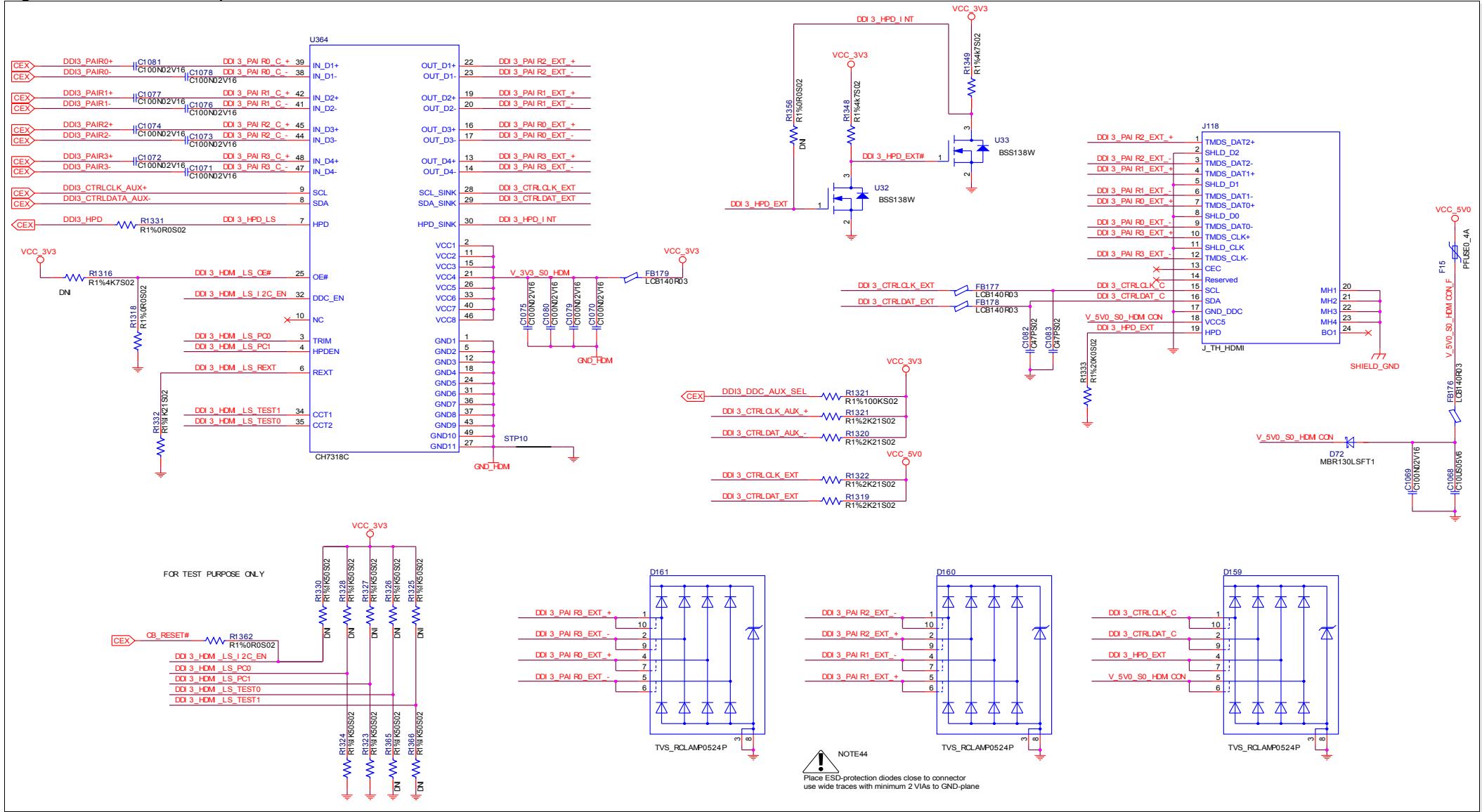
A Dual-mode source Module requires level shifters on the Carrier to convert the low-swing AC coupled differential pairs from the video source to HDMI compliant current mode differential outputs. The example schematics use a Chrontel CH7318C translator which supports data rates up to 1.65GB/s per lane. FET based passive level translators can be used for lower data rates. The DisplayPort AUX channel is configured as a DDC interface for HDMI. Further information on pre-emphasis as well as output current trim capabilities of the CH7318C can be found in the Chrontel datasheet.
See http://www.chrontel.com/index.php/ch7318c-hdmi-hdcp-dvi-transmitters for more information.
ESD clamping diodes D159, D160 and D161 protect the Module from external ESD events and should be placed near the HDMI connector. The pin-out of the ESD clamp diodes allows for a trace to run under the chip connector to two pins.
HDMI uses I2C signaling for the DDC. Resistors 1319 and 1322 provide the necessary pull-up. The FETs U32 and U33 provide the Hot Plug Detect signal
The Carrier provides 5V power to the HDMI connector. A series diode (D72) should be used to prevent back feeding of power in the event that the monitor is powered up when the Carrier is powered down.
The HDMI Hot Plug Detect signal is buffered by two FETs U32 and U33 which prevent back feeding of power from the display to the Module as well as level translation to 3.3V levels.
Note: The reference schematics assume that the Module’s DDI ports are dual-source capable – dual source indicates that the Module can output DisplayPort or HDMI/DVI based on the DDC\_AUX\_SEL signal.
# DVI Example
Figure 22: DVI Example
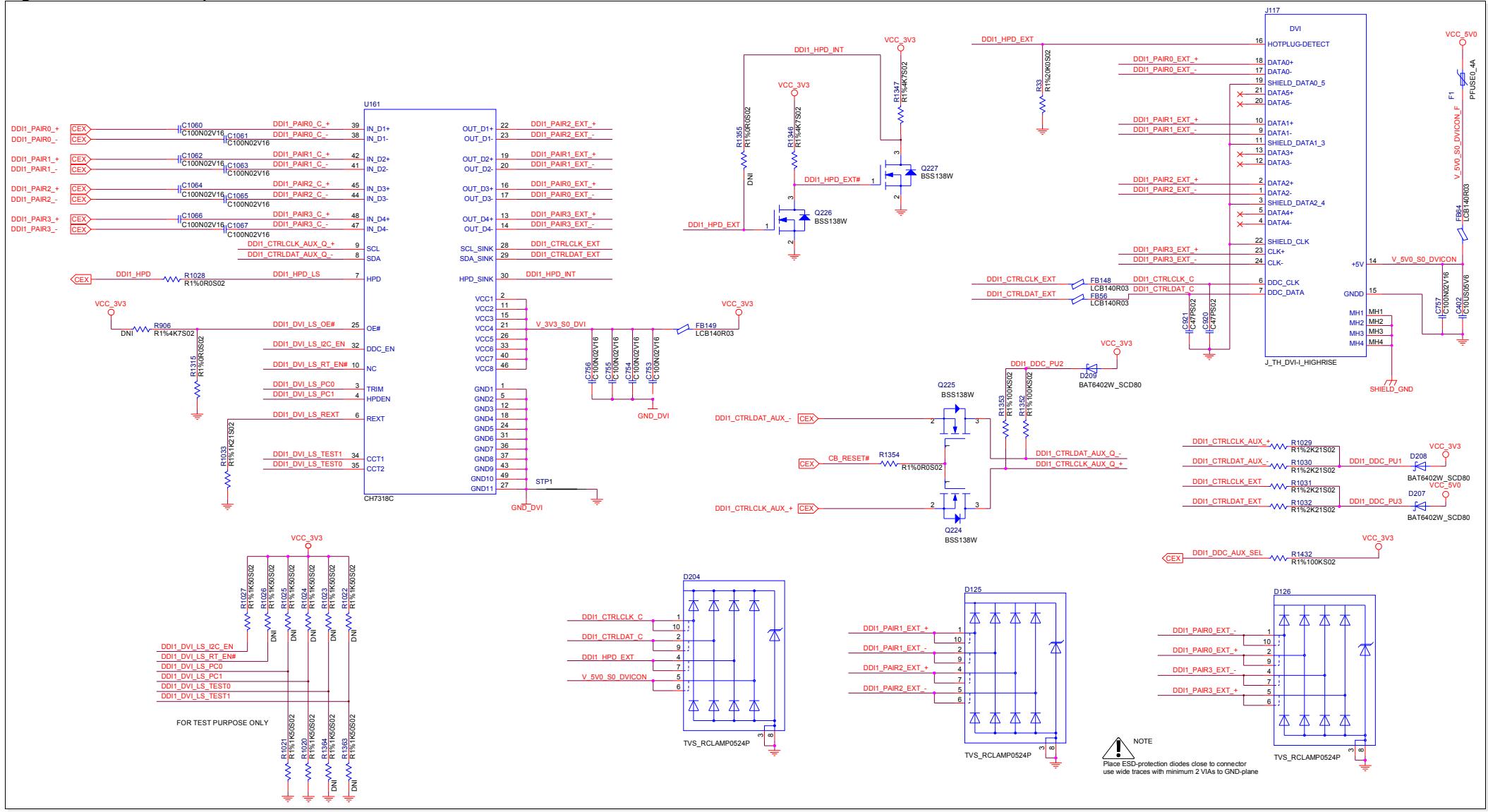
A Dual-mode source Module requires level shifters on the Carrier to convert the low-swing AC coupled differential pairs from the video source to DVI compliant current mode differential outputs. The example schematics use a Chrontel CH7318C translator which supports data rates up to 1.65GB/s per lane. FET based passive level translators can be used for lower data rates. The DisplayPort AUX channel is configured as a DDC interface for HDMI. Further information on pre-emphasis as well as output current trim capabilities of the CH7318C can be found in the Chrontel datasheet.
See http://www.chrontel.com/index.php/ch7318c-hdmi-hdcp-dvi-transmitters for more information.
ESD clamping diodes D125, D126 and D204 protect the Module from external ESD events and should be placed near the DVI connector. The pin-out of the ESD clamp diodes allows for a trace to run under the chip connector to two pins.
DVI uses I2C signaling for the DDC. Resistors 1031 and 1032 provide the necessary pull-up. The FETs Q226 and Q227 provide the Hot Plug Detect signal
The Carrier provides 5V power to the DVI connector.
Series diodes (D207, D208, D209) should be used to prevent back feeding of power in the event that the monitor is powered up when the Carrier is powered down.
The DDI1 Hot Plug Detect signal is buffered by two FETs Q226 and Q227 which prevent back feeding of power from the display to the Module as well as level translation to 3.3V levels.
# Note: The reference schematics assume that the Module’s DDI ports are dual-source capable – dual source indicates that the Module can output DisplayPort or HDMI/DVI based on the DDC\_AUX\_SEL signal.
Other DisplayPort Output Options: LVDS, VGA, etc.
Other display interfaces can be created from DisplayPort, but this needs an active interface change. DisplayPort to LVDS can be created with interface chips from multiple vendors. One example is the Chrontel CH7511.
DisplayPort to VGA interface chips are available from multiple vendors including Chrontel or NXP.
# Note: Please also follow the design guidelines from the chip vendor
# 2.5.1.3. Routing Considerations
For the DisplayPort interconnection between the COM Express Module and the DisplayPort connector or the level shifter, refer to Section 6.5.6 'DisplayPort Trace Routing Guidelines' on page 186 for details.
The Digital Video Interface (DVI) and the High Definition Multimedia Interface (HDMI) are based on the differential signaling method TMDS. To achieve the full performance and reliability of HDMI and DVI, the TDMS differential signals between the level shifter and the DVI connector have to be routed in pairs with a differential impedance of 100Ω. The length of the differential signals must be kept as close to the same as possible. The maximum length difference must not exceed 100mils for any of the pairs relative to each other. Pair to pair spacing should be more than 2x the trace width to reduce trace-to-trace couplings. For example, having wider gaps between differential pair DVI traces will minimize noise coupling. It is also strongly advised that ground not be placed adjacent to the DVI traces on the same layer. There should be a minimum distance of 30mils between the DVI trace and any ground on the same layer.
# 2.5.2. SDVO
SDVO was developed by the Intel® Corporation to interface third party SDVO compliant display controller devices that may have a variety of output formats, including DVI, LVDS, HDMI and TV-Out. The electrical interface is based on the PCI Express interface, though the protocol and timings are completely unique. Whereas PCI Express runs at a fixed frequency, the frequency of the SDVO interface is dependent upon the active display resolution and timing.
# Note: As SDVO is not supported in future chipsets and graphic controllers it is not recommended to use this interface in future designs.
# 2.5.2.1. Signal Definitions
The SDVO interface of the COM Express Module features its own dedicated I²C bus (SDVO\_I2C\_CLK and SDVO\_I2C\_DAT). It is used to control the external SDVO devices and to read out the display timing data from the connected display.
Type 6 Modules allow one SDVO port on DDI[1]. The DDI port needs to be configured to be used as SDVO usually via the Module's BIOS.
On Type 2 Modules the pins for SDVO ports B and C are shared with the PEG port.
If the Type 2 Module supports SDVO, the Module graphics controller configures the PEG lines for SDVO operation if it detects that COM Express signals SDVO\_I2C\_CLK and SDVO\_I2C\_DATA are pulled high to 2.5V, and if the PEG\_ENABLE# line is left floating. This combination leaves the Module's internal graphics engine enabled but converts the output format to SDVO. The SDVO\_I2C\_CLK and SDVO\_I2C\_DATA lines are pulled to 2.5V on an ADD2 card.
For a device “down” SDVO converter, the SDVO\_I2C\_CLK and SDVO\_I2C\_DATA lines have to be pulled up to 2.5V on the Carrier Board and PEG\_ENABLE# left open.
# SDVO Port Configuration
The SDVO port and device configuration is fixed within the Intel® Graphics Video BIOS implementation of the COM Express Module. All COM Express Modules assume a I²C bus address 0111 000x for SDVO devices connected to port B and an I²C bus address of 0111 001x for SDVO devices connected to port C. Table 12 below lists the supported SDVO port configurations.
Table 12: SDVO Port Configuration
| SDVO Port B | SDVO Port C |
| Device Type | Selectable in BIOS Setup Program. | Selectable in BIOS Setup Program. |
| I2C Address | 0111 000x | 0111 001x |
| I2C Bus | SDVO I2C GPIO pins | SDVO I2C GPIO pins |
| DDC Bus | SDVO I2C GPIO pins | SDVO I2C GPIO pins |
# Supported SDVO Devices
Due to the fact that SDVO is an Intel® defined interface, the number of supported SDVO devices is limited to devices that are supported by the Intel® Graphics Video BIOS and Graphics Driver software.
Table 13: Intel® SDVO Supported Device Descriptions
| Device | Vendor | Type | Link |
| CH7021A | Chrontel | SDTV / HDTV | http://www.chrontel.com |
| CH7308A | Chrontel | LVDS | http://www.chrontel.com |
| CH7307C | Chrontel | DVI | http://www.chrontel.com |
| CH7312 | Chrontel | DVI | http://www.chrontel.com |
| CX25905 | Conexant | DVI-D / TV / CRT | http://www.conexant.com |
| SiL1362/1364 | Silicon Image | DVI | http://www.siliconimage.com |
| SiL 1390 | Silicon Image | HDMI | http://www.siliconimage.com |
Note: The devices listed in Table 13 require BIOS support for proper operation. Check with the Modules vendor for a list of specific devices that are supported.
# 2.5.2.2. Reference Schematics
# SDVO to DVI Transmitter Example
Figure 23: SDVO to DVI Transmitter Example
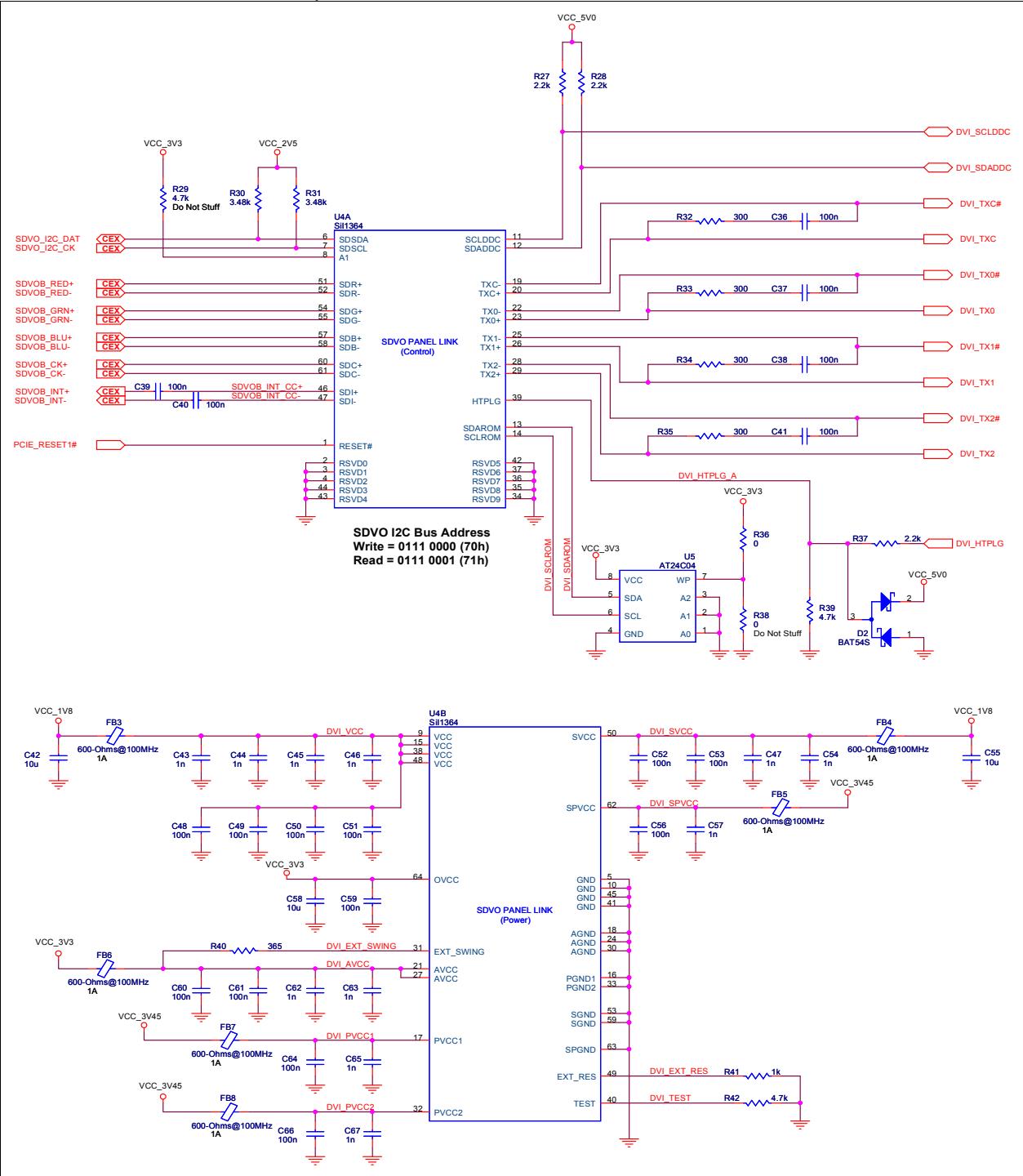
Figure 23 'SDVO to DVI Transmitter Example' above shows a single-channel, device-down application for SDVO to DVI implementation. A Silicon Image transmitter IC (SIL1364) converts SDVO signals from the Module to a DVI-D format. Pins are connected to the DVI-D Connector (Molex 74320-4004).
PEG\_RX1+ and PEG\_RX1- are sourced from COM Express Module pins C55 and C56 and are defined as SDVOB\_INT+ and SDVOB\_INT- in the COM Express Specification respectively. They are driven by SDI+ and SDI- from the chip. The PEG Receive interface on the COM Express Module is driven by the TX source (Interrupt) on the SDVO chip. The TX source needs to be AC-coupled near the source (SDI pins).
EXT\_RES is pulled low through a 1.0kΩ resistor to generate a reference-bias current.
PEG\_TX0+/- through PEG\_TX3- from COM Express Module pins are defined as SDVO\_RED+/-, GRN+/-, BLU+/- and CK+/- in the COM Express Specification respectively. They drive SDR+/-, SDG+/-, SDB+/- and SDC+/- on the chip. The PEG Transmit interface on the COM Express Module drives the RX load on the graphics chip.
SDVO\_I2C\_CLK and SDVO\_I2C\_DAT are sourced from COM Express Module pins D73 and C73 respectively. A pull-up to 2.5V using a 3.5kΩ resistor is required for both lines on the Carrier Board for a device-down application. For an SDVO slot design, pull-ups are on the SDVO plugin card.
The I2C Bus supports management functions and provides Manufacturer information, a model number, and a part number.
RESET# is driven by the PCI\_RESET1# from COM Express Module pin C23, PCI\_RESET#, after buffering. The signal resets the chip and causes initialization.
A1 establishes the I2C default address. Pulled Low = 0X70 (unconnected). Pulled High = 0X72 through a 4.7kΩ resistor.
HTPLUG – The Hot Plug input is driven by the Monitor Device, which causes the System OS to initiate a Plug and Play sequence that results in identifying the configuration of the Monitor. Protection diodes and a current-limiting resistor also are added.
TEST – The factory test pin needs to be tied low for normal operation.
EXT\_SWING should be tied to AVCC pins through a 360Ω resistor. It sets the amplitude voltage swing. Smaller values set a larger voltage swing and vice versa.
SDAROM and SCLROM interface to a non-volatile memory U17, Serial Prom AT24C04.
TX0+/- through TX2+/- DVI output pins are TMDS low voltage differential signals.
TXC+/- DVI Clock pins are TMDS low voltage differential signals.
SCLDDC and SDADDC should be pulled up with a 2.2kΩ resistor. They serve as the signals for the I2C interface to the DVI connector. The interface supports the DDC (Display Data Channel) standard for EDID (Extended Display Identification Data) over I2C. The EDID includes the manufacturer’s name, product type, phosphor or filter type, timings supported by the display, display size, luminance data and pixel mapping data (for digital displays only).
SDAROM and SCLROM external pull-ups are not required because they are internally pulled up. They serve as signals for the I2C interface to EEPROM AT24C04.
The schematics also show the requirements for decoupling and the filter caps for the SIL1364 graphics chip.
Other SDVO Output Options: LVDS, NTSC
SDVO to LVDS interface chips are available from multiple vendors. One example is the Chrontel CH7308.
SDVO to NTSC interface chips are available from multiple vendors including Chrontel.
# Note: Please also follow the design guidelines from the SDVO chip vendor
# 2.5.2.3. Routing Considerations
For the SDVO interconnection between the COM Express Module and a third-party SDVO compliant device, refer to Section 6.5.5. 'SDVO Trace Routing Guidelines' on page 185 below and to the layout and routing considerations specified by the SDVO device manufacturer.
The Digital Video Interface (DVI) is based on the differential signaling method TDMS. To achieve the full performance and reliability of DVI, the TDMS differential signals between the SDVO to DVI transmitter and the DVI connector have to be routed in pairs with a differential impedance of 100Ω. The length of the differential signals must be kept as close to the same as possible. The maximum length difference must not exceed 100mils for any of the pairs relative to each other. Spacing between the differential pair traces should be more than 2x the trace width to reduce trace-to-trace couplings. For example, having wider gaps between differential pair DVI traces will minimize noise coupling. It is also strongly advised that ground not be placed adjacent to the DVI traces on the same layer. There should be a minimum distance of 30mils between the DVI trace and any ground on the same layer. For more information, refer to the layout and routing considerations as specified by the manufacturer of the SDVO to DVI transmitter.
# SDVO Option – PEG Lane Reversal
If Module pin D54 PEG\_LANE\_RV# is strapped low to untwist a bowtie on the PEGx16 lines to an x16 slot, then an ADD2 card used in this slot must be a reverse pin-out ADD2 card. Reverse pin-out ADD2 cards are designated ADD2-R.
If the SDVO device is “down” on the Carrier Board, then the PEG\_LANE\_REV# pin has no effect because SDVO lines are not reversed on the chipset – only PCIe x16 lines are.
Please see the Lane Reversal caution at Section 2.4.4.2. 'Lane Reversal' on page 53 above.
# 2.6. Mobile PCI Express Module (MXM)
Mobile PCI Express Module is an interconnect standard for GPUs defined by the MXM-SIG, mainly used in laptops. The goal of this standard was to enable a user an easy way to upgrade the graphic card of a laptop without having to buy a hole new system or rely on proprietary vendor upgrades. This goal was achieved with a non-proprietary standard socket.
At this writing, the current generation of MXM is MXM3. Two Module sizes, designated as A and B, are allowed by MXM3 for different power envelopes and use cases.
Table 14: available MXM 3 Types
| MXM Type | Width | Length | Module Compatibility | Max. Power | GPU memory bus |
| MXM-A | 82mm | 70mm | A | 55W | 64-bit or 128-bit |
| MXM-B | 82mm | 105mm | A,B | 100W | 256-bit |
The MXM3-COM Express interface is over the COM Express PEG lines. The MXM3 outputs are MXM3 Module dependent and can include DisplayPort, HDMI, DVI or TVout.
# 2.6.1. Signal Definitions
The primary interface between the COM Express Module and the MXM is a x16 PCI Express bus. The Carrier contains the AC coupling caps for the PEG\_RX[0:15] signals, the COM Express Module contains the AC coupling caps for the PEG\_TX[0:15] signals.
Three power rails are supplied to the MXM 3.3V@1A, 5V@2.5A and 12V@ up to 10A. The power rails are powered during S0. In the schematics below the main power rail to the MXM3 Module is shown as a fixed 12V (VCC\_12V). An MXM3 Module can actually accept power over 7 to 20V range on this rail. Some COM Express Modules accept power over a similar range and if you are designing a battery powered system you may be able to take advantage of this wide range capability.
PEG\_CLK\_REQ# is used to enable the PCI Express clock PCIE\_CLKPEG when a MXM is installed. The clock does not run when a MXM is not installed, reducing emissions.
The SMBus is connected between the COM Express Module and the MXM. Zero ohm resistors R115 and R116 are used to allow the SMBus to be disconnected from the MXM in the event there are address or other conflicts.
Table 15: special MXM signals
| Signal | Signal Name | Signal Description |
| PEX_STD_SW# | PCI Express swing select | Pull-down resistor to ground determines the PCI Express voltage. PCI Express Gen1 and GEN2 select the correct resistor for short (resistor not installed), medium short (147K Ohm to ground), medium long (7.15K Ohm to ground), and long PCI Express channel length (0 Ohm to ground). Refer to the MXM specification for further information. |
| TH_OVERT# | Thermal shutdown request | The carrier must power down the MXM Module within 500 ms of assertion. |
| TH_PWM | Thermal PWM | May be used to control a fan on the MXM thermal solution. |
| PWR_OK | Power OK | Asserted by MXM card when all supplies are within tolerance. There is also a COM Express signal named “PWR_OK” which is not meant here. |
| PRSNT_R#/L# | MXM card presence detect | Tied to ground on the MXM card. Can be used by the carrier to detect that an MXM card is inserted |
The MXM3 Module shown in this example supports two DisplayPort channels. They are designated DP1 and DP3 on the schematic. The DP1 reference schematic has Dual Mode support which switches the AUX channel from a differential pair for Display Port to an I2C compatible interface for DVI/HDMI. FETs are provided to switch in pull-up resistors required for the I2C interface as well as removal of the blocking capacitors. The DP1 schematic should be replicated for DP3 as required.
The reference design does not support the discrete panel and backlight control signals found on the MXM connector pins 23 (PNL\_PWR\_EN), 25 (PNL\_BL\_PWM), and 27 (PNL\_BL\_PWM). The design relies on panel support for these interfaces via the AUX channel.
# 2.6.2. Reference Schematics
Figure 24: MXM Reference Schematics
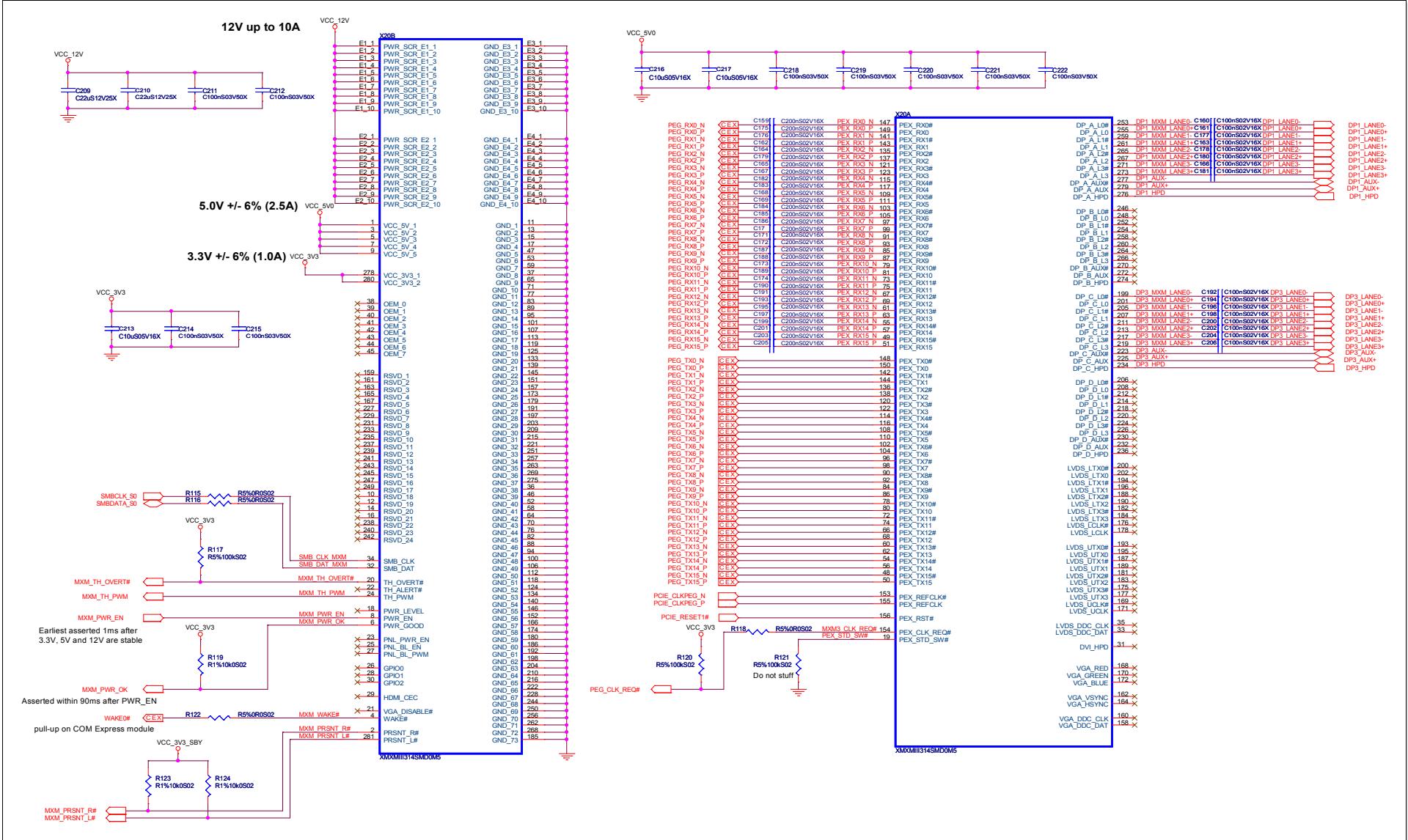
Figure 25: DisplayPort implementation of MXM interface (one channel)
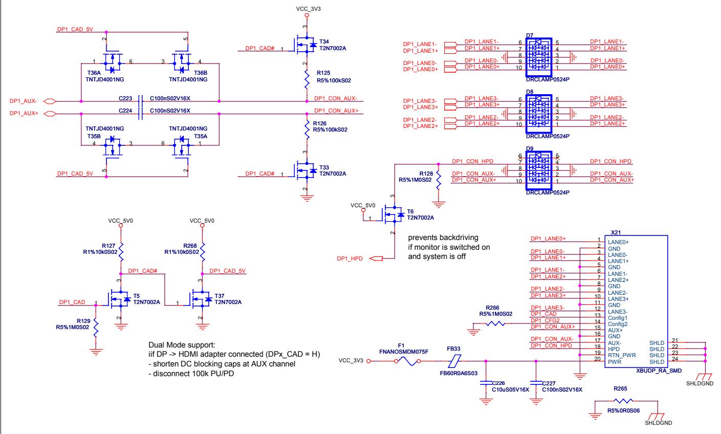
Following notes apply to Figure 24: MXM Reference Schematics and Figure 25: DisplayPort implementation of MXM interface (one channel).
The reference designs supports a MXM card with two Display Port interfaces. The primary interface between the Module and MXM Card is x16 PCI Express. The RX DC blocking capacitors reside on the Carrier, the TX DC blocking capacitors reside on the COM Express Module. A MXM card can support PCI Express Gen1, Gen2, or Gen3. The resistor R121 is used to set the PCI Express voltage swing. The SMBus can be used for sideband communication with the MXM Module. The MXM card is powered from the non-standby rail so the “S0” SMBus signals are used. MXM\_PWR\_EN should be asserted no sooner than 1ms after the power to the MXM card is stable. PEG\_CLK\_REQ# can be used to disable the PCI Express clock when a MXM card is not installed to minimize emissions.
The reference schematic shows a dual mode Display Port implementation. Diodes D7, D8, and D9 clamp ESD. T6 prevents back driving of voltage if the monitor is on and the carrier power is off. FETs T5 and T37 level shift the cable adapter detect signal. The cable adapter detect is used to select between HDMI and Display Port. When HDMI is selected, the AUX channel is used as an I2C interface. The DC blocking capacitors are removed (shorted out) and pull-ups enabled. When Display Port is selected the AUX channel is a differential pair with the DC blocking capacitors.
# 2.6.3. Routing Considerations
MXM card power requirements can be large. Note that the MXM specification allows up to 10A of 12V, 2.5A of 5V and 1A of 3.3V. Use appropriate trace width and number of vias to deliver the required power. The PCI Express signals should follow the routing guidelines found in chapter 2.4.4. 'Routing Considerations' on page 53 above.
# 2.7. LAN
All COM Express Modules provide at least one LAN port. The 8-wire 10/100/1000BASE-T Gigabit Ethernet interface compliant to the IEEE 802.3-2005 specification is the preferred interface for this port, with the COM Express Module PHY responsible for implementing auto-negotiation of 10/100BASE-TX vs 10/100/1000BASE-T operation. The carrier may also support a 4-wire 10/100BASE-TX interface from the COM Express Module on an exception basis. Check with your vendor for 10/100 only implementations.
# 2.7.1. Signal Definitions
The LAN interface of the COM Express Module consists of 4 pairs of low voltage differential pair signals designated from 'GBE0\_MDI0' (+ and -) to 'GBE0\_MDI3' (+ and -) plus additional control signals for link activity indicators. These signals can be used to connect to a 10/100/1000BASE-T RJ45 connector with integrated or external isolation magnetics on the Carrier Board. The corresponding LAN differential pair and control signals can be found on rows A and B of the Module's connector, as listed in Table 16 below.
Table 16: LAN Interface Signal Descriptions
| Signal | Pin# | Description | I/O | Comment |
| GBE0_MDI0+GBE0_MDI0- | A13A12 | Media Dependent Interface (MDI) differential pair 0. The MDI can operate in 1000, 100, and 10Mbit/sec modes. | I/O GBE | This signal pair is used for all modes. |
| GBE0_MDI1+GBE0_MDI1- | A10A9 | Media Dependent Interface (MDI) differential pair 1. The MDI can operate in 1000, 100, and 10Mbit/sec modes. | I/O GBE | This signal pair is used for all modes. |
| GBE0_MDI2+GBE0_MDI2- | A7A6 | Media Dependent Interface (MDI) differential pair 2. The MDI can operate in 1000, 100, and 10Mbit/sec modes. | I/O GBE | This signal pair is only used for 1000Mbit/sec Gigabit Ethernet mode. |
| GBE0_MDI3+GBE0_MDI3- | A3A2 | Media Dependent Interface (MDI) differential pair 3. The MDI can operate in 1000, 100, and 10Mbit/sec modes. | I/O GBE | This signal pair is only used for 1000Mbit/sec Gigabit Ethernet mode. |
| GBE0_CTREF | A14 | Reference voltage for Carrier Board Ethernet channel 0 magnetics center tap. | REF | |
| GBE0_LINK# | A8 | Ethernet controller 0 link indicator, active low. | O 3.3VSuspendOD CMOS | |
| GBE0_LINK100# | A4 | Ethernet controller 0 100Mbit/sec link indicator, active low. | O 3.3VSuspendOD CMOS | |
| GBE0_LINK1000# | A5 | Ethernet controller 0 1000Mbit/sec link indicator, active low. | O 3.3VSuspendOD CMOS | |
| GBE0_ACT# | B2 | Ethernet controller 0 activity indicator, active low. | O 3.3VSuspendOD CMOS | |
# 2.7.1.1. Status LED Signal Definitions
The four link status signals (LINK#, LINK100#, LINK1000#, and ACT#) are combined on the carrier to drive two status LEDs (Link Activity and Link Speed). These two LEDs are typically integrated into the RJ45 receptacle housing for the Ethernet, but may be placed on the carrier Module assembly as discrete LEDs. The most common functional characteristics for each LED are listed in Table 17 below.
Table 17: LAN Interface LED Function
| LED-Function | LED Color# | LED State | Description |
| Link Speed | Green / Orange | Off | 10 Mbps link speed |
| Green | 100 Mbps link speed |
| Orange | 1000 Mbps link speed |
| Link Status & Activity | Yellow | Off | No Link |
| Steady On | Link established, no activity detected |
| Blinking | Link established, activity detected |
# 2.7.1.2. LAN 1 and 2 shared with IDE
The Type 2 COM Express Module only provides one LAN port to the carrier. Type 3 and 5 COM Express Modules provide two additional 10/100/1000BASE-T Gigabit Ethernet ports in place of the IDE port, and Type 5 Module definitions include an option to support 10 Gigabit Ethernet port operation.
This Design Guide does not explicitly define Carrier Board support for the Type 3 and 5 COM Express Modules. However, it is recommended that a carrier supporting one of those Modules should follow the guidelines for the LAN 0 port carrier circuit in this section when defining the LAN 1 and 2 port carrier circuits.
# 2.7.1.3. PHY / Magnetics Connections
The COM Express Module specification partitions the IEEE 802.3 PHY / MDI interface circuit resources between the Module and carrier, with the PHY located on the Module and the coupling magnetics located on the carrier, preferably physically integrated in the RJ-45 receptacle housing associated with the port. Section 5.4.5 of the COM Express Module specification shows this circuit topology and provides a high level signal attenuation budget for Ethernet signals traversing this circuit.
In order to meet the signal performance requirements for MDI signals as defined in the IEEE 802.3-2005 specification and to ensure maximum interoperability of COM Express Modules and carriers, the PHY / Magnetics circuit should be implemented using the following guidelines:
The carrier should provide a full 8-wire (10/100/1000BASE-T) interface circuit to the COM Express Module
● Any secondary side resistive terminations required by the Module PHY will be present on the Module and are not on the Carrier
The center tap reference signal should be routed from the COM Express Module connector to the secondary side center tap of each transformer as defined in the IEEE 802.3-2005 specification, without any series resistance or impedance circuits
The Carrier Board design should utilize a coupling transformer capable of interoperating with the largest possible number of PHY devices
The Carrier Board design should have the primary side and secondary side center tap termination components (75 Ω resistors and 100 nF capacitors, respectively) placed physically as close to the coupling transformer as possible
The coupling transformer should be placed no further than 100mm (3.9”) from the COM Express Module connector on the Carrier Board.
It is recommended that the carrier use a RJ-45 connector with an integrated transformer. However, if a discrete coupling transformer is used, the transformer must be placed no further than 25mm (1.0”) from the RJ-45 receptacle.
As there are a large number of Ethernet PHY components and coupling transformers on the market, it is strongly recommended that the Carrier Board vendor document the transformer used in this interface circuit, in order to facilitate interoperability analysis between Modules and carriers. It is also recommended that the COM Express Module vendor identify the specific PHY component used in the LAN 0 interface on the Module.
# 2.7.2. Reference Schematics
# 2.7.2.1. Magnetics Integrated Into RJ-45 Receptacle
Figure 26: Magnetics Integrated Into RJ-45 Receptacle
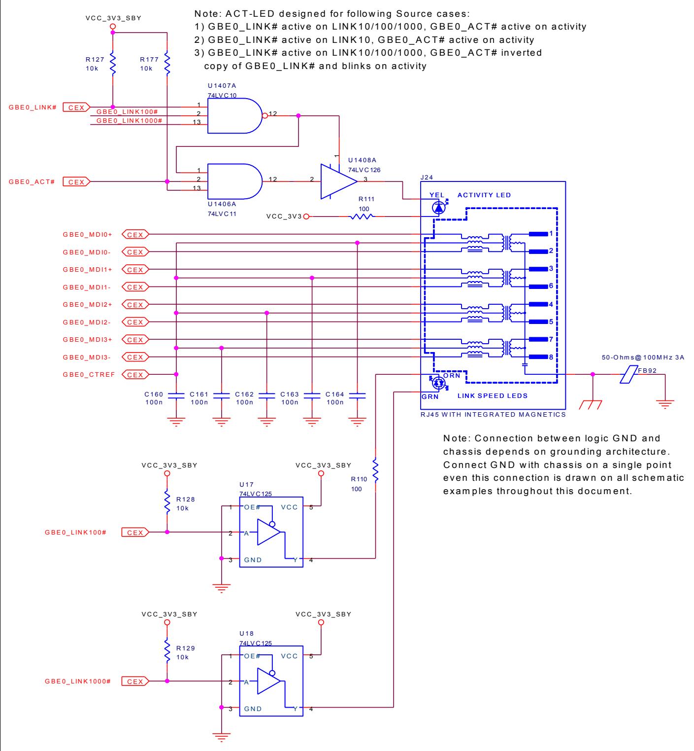
# 2.7.2.2. Discrete Coupling Transformer
Figure 27: Discrete Coupling Transformer
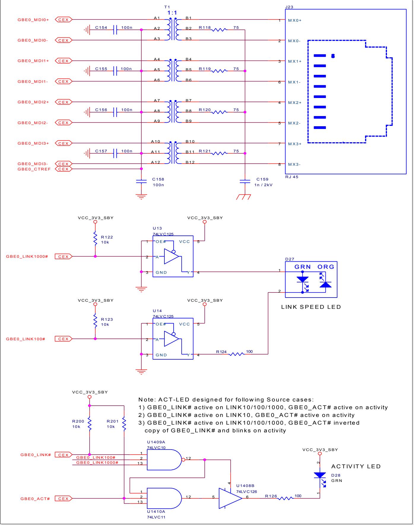
# 2.7.3. Routing Considerations
The 8-wire PHY / MDI circuit is required to meet a specific waveform template and associated signal integrity requirements defined in the IEEE 802.3-2005 specification. In order to meet these requirements, the routing rules in Section 6.5.7. 'LAN Trace Routing Guidelines' on page 187 should be observed on the Carrier Board.
The four status signals driven by the COM Express Module to the Carrier Board are low frequency signals that do not have any signal integrity or trace routing requirements beyond generally accepted design practices for such signals.
# 2.7.3.1. Reference Ground Isolation and Coupling
The Carrier Board should maintain a well-designed analog ground plane around the components on the primary side of the transformer between the transformer and the RJ-45 receptacle. The analog ground plane is bonded to the shield of the external cable through the RJ-45 connector housing.
The analog ground plane should be coupled to the carrier’s digital logic ground plane using a capacitive coupling circuit that meets the ground plane isolation requirements defined in the 802.3-2005 specification. It is recommended that the Carrier Board PCB design maintain a minimum 30 mil gap between the digital logic ground plane and the analog ground plane.
It's recommended to place an optional GND to SHIELDGND connection near the RJ-45 connector to improve EMI and ESD capabilities.
# 2.8. USB Ports
A COM Express Module must support a minimum of 4 USB Ports and can support up to 8 USB Ports. All of the USB Ports must be USB2.0 compliant. There are 4 over-current signals shared by the 8 USB Ports. A Carrier must current limit the USB power source to minimize disruption of the Carrier in the event that a short or over-current condition exists on one of the USB Ports. A Module must fill the USB Ports starting at Port 0. The USB SuperSpeed ports 0, 1, 2 and 3, if used, are to be paired with USB 2.0 ports 0, 1, 2 and 3 in the same order. The USB SuperSpeed ports use the same over current signaling mechanism as the USB 2.0 ports, but USB 3.0 allows up to 1A current per port instead of 500mA allowed in USB 2.0. Although USB 2.0 signals use differential signaling, the USB specification also encodes single ended state information in the differential pair, making EMI filtering somewhat challenging. Ports that are internal to the Carrier do not need EMI filters. A USB Port can be powered from the Carrier Main Power or from the Carrier Suspend Power. Main Power is used for USB devices that are accessed when the system is powered on. Suspend Power (VCC\_5V\_SBY) is used for devices that need to be powered when the Module is in Sleep-State S5. This would typically be for USB devices that support Wake-on-USB. The amount of current available on VCC\_5V\_SBY is limited so it should be used sparingly.
# 2.8.1. Signal Definitions
All USB Ports appear on the COM Express A-B connector as shown in Table 18 below.
# 2.8.1.1. USB Over-Current Protection (USB\_x\_y\_OC#)
The USB Specification describes power distribution over the USB port, which supplies power for USB devices that are directly connected to the Carrier Board. Therefore, the host must implement over-current protection on the ports for safety reasons. Should the aggregate current drawn by the downstream ports exceed a permitted value, the over-current protection circuit removes power from all affected downstream ports. The over-current limiting mechanism must be resettable without user mechanical intervention. For more detailed information about this subject, refer to the 'Universal Serial Bus Specifications Revision 2.0', which can be found on the website http://www.usb.org.
Over-current protection for USB ports can be implemented by using power distribution switches on the Carrier Board that monitor the USB port power lines. Power distribution switches usually have a soft-start circuitry that minimizes inrush current in applications where highly capacitive loads are employed. Transient faults are internally filtered.
Additionally, they offer a fault status output that is asserted during over-current and thermal shutdown conditions. These outputs should be connected to the corresponding COM Express Modules USB over-current sense signals. Fault status signaling is an option at the USB specification. If you don't need the popup message in your OS you may leave the signals USB\_0\_1\_OC#, USB\_2\_3\_OC#, USB\_4\_5\_OC# and USB\_6\_7\_OC# unconnected.
Simple resettable PolySwitch devices are capable of fulfilling the requirements of USB overcurrent protection and therefore can be used as a replacement for power distribution switches.
Fault status signals are connected by a pullup resistor to VCC\_3V3\_SBY on COM Express Module. Please check your tolerance on a USB port with VCC\_5V supply.
# 2.8.1.2. Powering USB devices during S5
The power distribution switches and the ESD protection shown in the schematics can be powered from Main Power or Suspend Power (VCC\_5V\_SBY). Ports powered by Suspend Power are powered during the S3 and S5 system states. This provides the ability for the COM Express Module to generate system wake-up events over the USB interface.
Table 18: USB Signal Description
| Signal | Pin # | Description | I/O | Comment |
| USB0+ | A46 | USB Port 0, data + or D+ | I/O USB | mandatory on Module |
| USB0- | A45 | USB Port 0, data - or D- | I/O USB | mandatory on Module |
| USB1+ | B46 | USB Port 1, data + or D+ | I/O USB | mandatory on Module |
| USB1- | B45 | USB Port 1, data - or D- | I/O USB | mandatory on Module |
| USB2+ | A43 | USB Port 2, data + or D+ | I/O USB | mandatory on Module |
| USB2- | A42 | USB Port 2, data - or D- | I/O USB | mandatory on Module |
| USB3+ | B43 | USB Port 3, data + or D+ | I/O USB | mandatory on Module |
| USB3- | B42 | USB Port 3, data - or D- | I/O USB | mandatory on Module |
| USB4+ | A40 | USB Port 4, data + or D+ | I/O USB | optional on Module |
| USB4- | A39 | USB Port 4, data - or D- | I/O USB | optional on Module |
| USB5+ | B40 | USB Port 5, data + or D+ | I/O USB | optional on Module |
| USB5- | B39 | USB Port 5, data - or D- | I/O USB | optional on Module |
| USB6+ | A37 | USB Port 6, data + or D+ | I/O USB | optional on Module |
| USB6- | A36 | USB Port 6, data - or D- | I/O USB | optional on Module |
| USB7+ | B37 | USB Port 7, data + or D+ | I/O USB | optional on Module |
| USB7- | B36 | USB Port 7, data - or D- | I/O USB | optional on Module |
| USB_0_1_OC# | B44 | USB over-current sense, USB ports 0 and 1. | I 3.3V CMOS | optional on Module |
| USB_2_3_OC# | A44 | USB over-current sense, USB ports 2 and 3. | I 3.3VCMOS | optional on Module |
| USB_4_5_OC# | B38 | USB over-current sense, USB ports 4 and 5. | I 3.3V CMOS | optional on Module |
| USB_6_7_OC# | A38 | USB over-current sense, USB ports 6 and 7. | I 3.3V CMOS | optional on Module |
# 2.8.1.3. USB connector
Figure 28: USB Connector
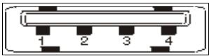
Table 19: USB Connector Signal Description
| Signal | Pin | Description | I/O | Comment |
| VCC | 1 | +5V Power Supply | P 5V | Must be current-limited for external devices |
| -DATA | 2 | Universal Serial Bus Data, negative differential signal. | I/O USB | |
| +DATA | 3 | Universal Serial Bus Data, positive differential signal. | I/O USB | |
| GND | 4 | Ground | P | |
# 2.8.2. Reference Schematics
The following notes apply to Figure 29 below.
J6 incorporate an USB Type A receptacle. J58 has two of them and in addition, includes an RJ-45 (Foxconn UB11123-J51, Pulse JW0A1P0R-E).
The reference design uses an over-current detection and protection device. Two examples are the Texas Instruments TPS2042AD and the Micrel MIC2026 dual channel power distribution switch. The second example includes a discrete implementation.
The first schematic is powered from VCC\_5V\_SBY Suspend power and can provide Wake on LAN support. The second schematic is powered using 5V.
Power to the USB Port is filtered using a ferrite (90 Ω @100MHz, 3000mA) to minimize emissions. The ferrite should be placed adjacent to the USB Port connector pins.
USB\_0\_1\_OC# and USB\_2\_3\_OC# are over-current signals that are inputs to COM Express Module. Each signal is driven low upon detection of overload, short-circuit or thermal trip, which causes the affected USB Port power to turn off. Do not attach pull-ups to the OC signals on the COM Express Carrier Board; this is done on the COM Express Module.
The OC# signal is asserted until the over-current or over-temperature condition is resolved.
USB0+/- through USB2+/- from the COM Express Module are routed through a common mode choke to reduce radiated cable emissions. The part shown is a Coilcraft 0805USB-901MLC; this device has a common mode impedance of approximately 90 Ω at 100MHz. The common-mode choke should be placed close to the USB connector.
ESD protection diodes D1 and D2 provide overvoltage protection caused by ESD and electrical fast transients . Low capacitance diodes and transient voltage suppression diodes should be placed near the USB connector. The example design uses a SR05 RailClamp surge diode array DATVSSR05 from Semtech (http://semtech.com).
The example designs show a ferrite connecting Chassis Ground and Logic Ground at the USB connector. Many USB devices connect Chassis and Logic grounds together. To minimize the current in this path a ferrite or capacitor connecting Chassis Ground to Logic Ground should be placed close to the USB connector.
Figure 29: USB Reference Design
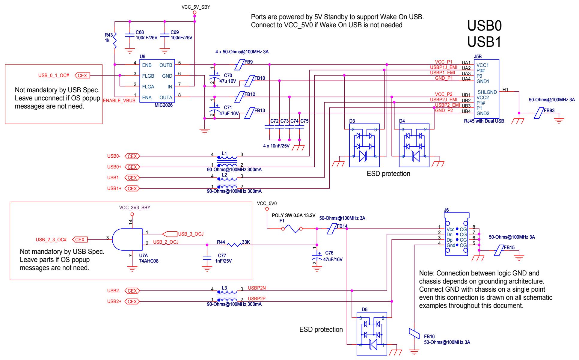
# 2.8.3. Avoiding Back-driving Problems
For more information please refer to chapter 2.9.3 'Avoiding Back-driving Problems' on page 86 below.
# 2.8.4. Routing Considerations
Route USB signals as differential pairs, with a 90-Ω differential impedance and a 45-Ω, singleended impedance. Ideally, a USB pair is routed on a single layer adjacent to a ground plane.
USB pairs should not cross plane splits. Keep layer transitions to a minimum. Reference USB pairs to a power plane if necessary. The power plane should be well-bypassed. Section 6.5.2. 'USB Trace Routing Guidelines' on page 183 summarizes USB routing rules.
# 2.8.4.1. EMI / ESD Protection
To improve the EMI behavior of the USB interface, a design should include common mode chokes, which have to be placed as close as possible to the USB connector signal pins. Common mode chokes can provide required noise attenuation but they also distort the signal quality of full-speed and high-speed signaling. Therefore, common mode chokes should be chosen carefully to meet the requirements of the EMI noise filtering while retaining the integrity of the USB signals on the Carrier Board design.
To protect the USB host interface of the Module from over-voltage caused by electrostatic discharge (ESD) and electrical fast transients (EFT), low capacitance steering diodes and transient voltage suppression diodes have to be implemented on the Carrier Board design. In the USB reference schematics Figure 29 above, this is implemented by using 'SR05 RailClamp®' surge rated diode arrays from Semtech (http://semtech.com).
# 2.9. USB 3.0
USB 3.0 is the third major revision of the Universal Serial Bus (USB) standard for computer connectivity. It adds a new transfer speed called SuperSpeed (SS) to the already existing LowSpeed (LS), FullSpeed (FS) and HighSpeed (HS).
USB 3.0 leverages the existing USB 2.0 infrastructure by adding two additional data pair lines to allow a transmission speed up to 5 Gbit/s, which is 10 times faster than USB 2.0 with 480 Mbit/s. The additional data lines are unidirectional instead of the bidirectional USB 2.0 data lines.
USB 3.0 is fully backward compatible to USB 2.0. USB 3.0 connectors are different from USB 2.0 connectors. The USB 3.0 connector is a super set of a USB 2.0 connector, with 4 additional pins that are invisible to USB 2.0 connectors. A USB 2.0 Type A plug may be used in a USB 3.0 Type A receptacle, but the USB 3.0 SuperSpeed functions will not be available.
# 2.9.1. Signal Definitions
Type 10 offers up to 2 USB 3.0 ports and Type 6 up to 4.
Table 20: USB 2.0 Differential Lines
| Signal | Pins T6 | Pins T10 | Description | I/O |
| USB0+ | A46 | A46 | USB Port 0, data + or D+ | I/O USB |
| USB0- | A45 | A45 | USB Port 0, data - or D- | I/O USB |
| USB1+ | B46 | B46 | USB Port 1, data + or D+ | I/O USB |
| USB1- | B45 | B45 | USB Port 1, data - or D- | I/O USB |
| USB2+ | A43 | | USB Port 2, data + or D+ | I/O USB |
| USB2- | A42 | | USB Port 2, data - or D- | I/O USB |
| USB3+ | B43 | | USB Port 3, data + or D+ | I/O USB |
| USB3- | B42 | | USB Port 3, data - or D- | I/O USB |
Table 21: USB Overcurrent Protection lines
| Signal | Pins T6 | Pins T10 | Description | I/O |
| USB_0_1_OC# | B44 | B44 | USB over-current sense, USB channels 0 and 1. | I CMOS |
| USB_2-3_OC# | A44 | | USB over-current sense, USB channels 2 and 3. | I CMOS |
Table 22: USB 3.0 Differential Lines
| Signal | Pins T6 | Pins T10 | Description | I/O |
| USB_SSTX0+ | D4 | B23 | USB Port 0, SuperSpeed TX + | O PCIE |
| USB_SSTX0- | D3 | B22 | USB Port 0, SuperSpeed TX - | O PCIE |
| USB_SSTX1+ | D7 | B26 | USB Port 1, SuperSpeed TX + | O PCIE |
| USB_SSTX1- | D6 | B25 | USB Port 1, SuperSpeed TX - | O PCIE |
| USB_SSTX2+ | D10 | | USB Port 2, SuperSpeed TX + | O PCIE |
| USB_SSTX2- | D9 | | USB Port 2, SuperSpeed TX - | O PCIE |
| USB_SSTX3+ | D13 | | USB Port 3, SuperSpeed TX + | O PCIE |
| USB_SSTX3- | D12 | | USB Port 3, SuperSpeed TX - | O PCIE |
| USB_SSRX0+ | C4 | A23 | USB Port 0, SuperSpeed RX + | I PCIE |
| USB_SSRX0- | C3 | A22 | USB Port 0, SuperSpeed RX - | I PCIE |
| USB_SSRX1+ | C7 | A26 | USB Port 1, SuperSpeed RX + | I PCIE |
| USB_SSRX1- | C6 | A25 | USB Port 1, SuperSpeed RX - | I PCIE |
| USB_SSRX2+ | C10 | | USB Port 2, SuperSpeed RX + | I PCIE |
| USB_SSRX2-USB_SSRX3+ | C9C13 | | USB Port 2, SuperSpeed RX -USB Port 3, SuperSpeed RX + | I PCIEI PCIE |
| USB_SSRX3- | C12 | | USB Port 3, SuperSpeed RX - | I PCIE |
# 2.9.1.1. USB Differential lines (USB[0:3/1]+/-)
These signals fully comply to the USB 2.0 implementation and are described in chapter 2.8.1 'Signal Definitions' on page 76 above.
# 2.9.1.2. USB Over-Current Protection (USB\_x\_y\_OC#)
The USB Specification describes power distribution over the USB port, which supplies power for USB devices that are directly connected to the Carrier Board. Therefore, the host must implement over-current protection on the ports for safety reasons. Should the aggregate current drawn by the downstream ports exceed a permitted value, the over-current protection circuit removes power from all affected downstream ports. The over-current limiting mechanism must be resettable without user mechanical intervention. For more detailed information about this subject, refer to the 'Universal Serial Bus Specifications Revision 2.0', which can be found on the website http://www.usb.org.
Over-current protection for USB ports can be implemented by using power distribution switches on the Carrier Board that monitor the USB port power lines. Power distribution switches usually have a soft-start circuitry that minimizes inrush current in applications where highly capacitive loads are employed. Transient faults are internally filtered.
Additionally, they offer a fault status output that is asserted during over-current and thermal shutdown conditions. These outputs should be connected to the corresponding COM Express Modules USB over-current sense signals. Fault status signaling is an option at the USB specification. If you don't need the popup message in your OS you may leave the signals USB\_0\_1\_OC#, USB\_2\_3\_OC#, USB\_4\_5\_OC# and USB\_6\_7\_OC# unconnected.
Fault status signals are connected by a pullup resistor to VCC\_3V3\_SBY on COM Express Module. Please check your tolerance on a USB port with VCC\_5V supply.
USB 2.0 port's VCC current limit should be set to 500mA. For USB 3.0 implementations, the VCC current limit is raised to 1A. A different, USB 3.0 compatible, power switch is used.
# 2.9.1.3. USB 3.0 connector
Figure 30: USB 3.0 Connector
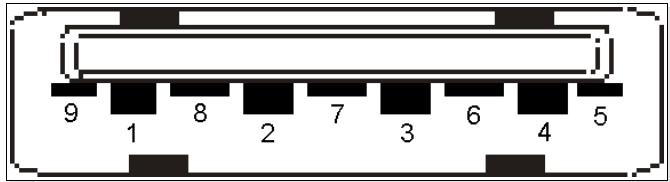
Table 23: USB 3.0 Connector Signal Description
| Signal | Pin | Description | I/O | Comment |
| VCC | 1 | +5V Power Supply | P 5V | Must be current-limited for external devices |
| -DATA | 2 | Universal Serial Bus Data, negative differential signal. | I/O USB | |
| +DATA | 3 | Universal Serial Bus Data, positive differential signal. | I/O USB | |
| GND | 4 | Ground | P | |
| SS_RX- | 5 | SuperSpeed Data Receive - | I PCIE | |
| SS_RX+ | 6 | SuperSpeed Data Receive + | I PCIE | |
| GND | 7 | Ground | P | |
| SS_TX- | 8 | SuperSpeed Data Receive - | O PCIE | |
| SS_TX+ | 9 | SuperSpeed Data Receive + | O PCIE | |
# 2.9.2. Reference Schematics
# 2.9.2.1. USB 3.0 Example
Figure 31: USB 3.0 Example Schematic
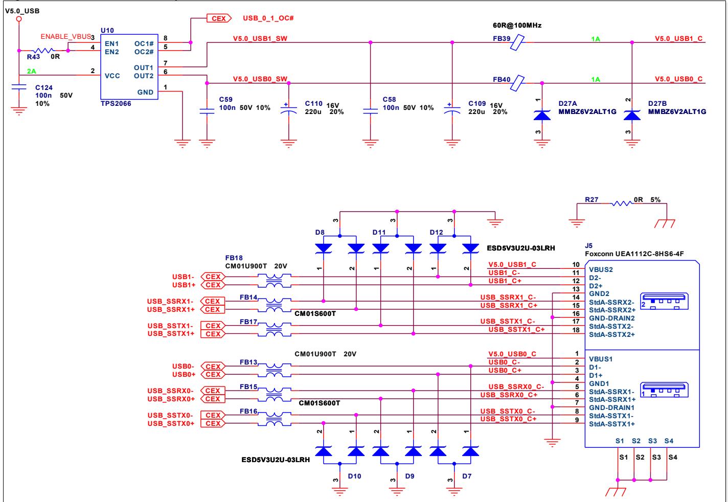
J5 incorporates a dual USB 3.0 Type A host receptacle. Note that the SuperSpeed pins are separate from the USB 2.0 pins.
This reference design uses an over-current detection and protection device (U10) dedicated for USB 3.0 with 1A current limit on each USB supply voltage line.
USB\_0\_1\_OC# is an over-current signal that is input to COM Express Module. The signal is driven low upon detection of overload, short-circuit or thermal trip, which causes the affected USB Port power to turn off. Do not attach pull-ups to the OC signals on the COM Express Carrier Board; this is done on the COM Express Module.
The OC# signal is asserted until the over-current or over-temperature condition is resolved.
USB0+/- through USB1+/- from the COM Express Module are routed through a common mode choke to reduce radiated cable emissions. The part shown is a Taiyo Yuden CM01U900T; this device has a common mode impedance of approximately 90 Ω at 100MHz. The common-mode choke should be placed close to the USB connector. The SuperSpeed Signals
USB\_SSR/TX0+/- through USB\_SSR/TX1+/- from the COM Express Module are also routed through a common mode choke to reduce radiated cable emissions. The part shown is a Taiyo Yuden CM01S600T; this device has a common mode impedance of approximately 60 Ω at 100MHz. The common-mode choke should be placed close to the USB connector.
ESD protection diodes D7 through D12 provide overvoltage protection caused by ESD and electrical fast transients . Low capacitance diodes and transient voltage suppression diodes should be placed near the USB connector. The example design uses an Ultra-Low capacitance ESD diode array from Infineon. (http://www.infineon.com).
The example designs show a 0 Ohm resistor connecting Chassis Ground and Logic Ground at the USB connector. Many USB devices connect Chassis and Logic grounds together. To minimize the current in this path a ferrite, resistor or capacitor connecting Chassis Ground to Logic Ground should be placed close to the USB connector.
# 2.9.3. Avoiding Back-driving Problems
Figure 32: Avoiding Back-driving
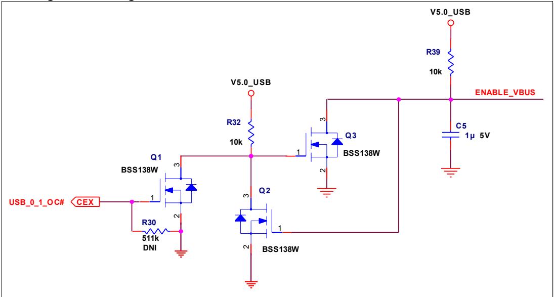
Back driving of power from a USB device to power rails on the Module can occur in some designs. It is recommended that USB power not be enabled until the Module's standby power rail (and therefore USB host power) is active. The COM Express standard does not provide a signal from the Module to the Carrier indicating the chipset standby rail is up. This reference schematic takes advantage of the USB\_0\_1\_OC# pin as an indication of USB Host power. This pin which is typically pulled up on the Module to the correct standby rail, may be used as shown here to enable USB power. The FETs Q1, Q2 and Q3 form a latch and ensure that in case of an over-current event no toggling situation will occur. To use this circuit do not install R43 in Figure 31: USB 3.0 Example Schematic and put instead the schematic in Figure 32: Avoiding Backdriving. There may be other circuit implementations that perform the same functionality.
# 2.9.4. Routing Considerations
Route USB data signals as differential pairs, with a 90-Ω differential impedance and a 45-Ω, single-ended impedance. Route USB SuperSpeed signals as differential pairs, with an 85-Ω differential impedance and a 50-Ω, single-ended impedance. Ideally, a USB pair is routed on a single layer adjacent to a ground plane.
USB pairs should not cross plane splits. Keep layer transitions to a minimum. Reference USB pairs to a power plane if necessary. The power plane should be well-bypassed. Section 6.5.3 'USB 3.0 Trace Routing Guidelines' on page 184 summarizes routing rules for SuperSpeed signals. Section 6.5.2 'USB Trace Routing Guidelines' on page 183 below summarizes routing rules for USB data signals.
# 2.9.4.1. EMI / ESD Protection
To improve the EMI behavior of the USB interface, a design should include common mode chokes, which have to be placed as close as possible to the USB connector signal pins. Common mode chokes can provide required noise attenuation but they also distort the signal quality of FullSpeed, HighSpeed and SuperSpeed signaling. Therefore, common mode chokes should be chosen carefully to meet the requirements of the EMI noise filtering while retaining the integrity of the USB signals on the Carrier Board design.
To protect the USB host interface of the Module from over-voltage caused by electrostatic discharge (ESD) and electrical fast transients (EFT), low capacitance steering diodes and transient voltage suppression diodes have to be implemented on the Carrier Board design. In Figure 31: USB 3.0 Example Schematic on page 84 above, this is implemented by using Ultra-Low capacitance ESD diode arrays from Infineon. (http://www.infineon.com).
# 2.10. SATA
Support for up to four SATA ports is defined on the COM Express A-B connector. Support for a minimum of two ports is required for all Module Types. The COM Express Specification allows for both SATA-150 and SATA-300 implementations. Constraints for SATA-300 implementations are more severe than those for SATA-150. The COM Express Specification addresses both in the section on insertion losses.
SATA devices can be internal to the system or external. The eSATA specification defines the connector used for external SATA devices. The eSATA interface must be designed to prevent damage from ESD, comply with EMI limits, and withstand more insertion/removals cycles than standard SATA. A specific eSATA connector was designed to meet these needs. The eSATA connector does not have the “L” shaped key, and because of this, SATA and eSATA cables cannot be interchanged.
# 2.10.1. Signal Definitions
Table 24: SATA Signal Description
| Signal | Pin | Description | I/O | Comment |
| SATA0_RX+ | A19 | Serial ATA channel 0 | I SATA | |
| SATA0_RX- | A20 | Receive input differential pair. |
| SATA0_TX+ | A16 | Serial ATA channel 0 | O SATA | |
| SATA0_TX- | A17 | Transmit output differential pair. |
| SATA1_RX+ | B19 | Serial ATA channel 1 | I SATA | |
| SATA1_RX- | B20 | Receive input differential pair. |
| SATA1_TX+ | B16 | Serial ATA channel 1 | O SATA | |
| SATA1_TX- | B17 | Transmit output differential pair. |
| SATA2_RX+ | A25 | Serial ATA channel 2 | I SATA | |
| SATA2_RX- | A26 | Receive input differential pair. |
| SATA2_TX+ | A22 | Serial ATA channel 2 | O SATA | |
| SATA2_TX- | A23 | Transmit output differential pair. |
| SATA3_RX+ | B25 | Serial ATA channel 3 | I SATA | |
| SATA3_RX- | B26 | Receive input differential pair. |
| SATA3_TX+ | B22 | Serial ATA channel 3 | O SATA | |
| SATA3_TX- | B23 | Transmit output differential pair. |
| SATA_ACT# | A28 | Serial ATA activity LED. Open collector output pin driven during SATA command activity. | O 3.3V CMOS OC | Able to drive 10 mA |
Table 25: Serial ATA Connector Pin-out
| Pin | Signal | Description |
| 1 | GND | Ground |
| 2 | TX+ | Transmitter differential pair positive signal |
| 3 | TX- | Transmitter differential pair negative signal |
| 4 | GND | Ground |
| 5 | RX- | Receiver differential pair negative signal |
| 6 | RX+ | Receiver differential pair positive signal |
| 7 | GND | Ground |
Table 26: Serial ATA Power Connector Pin-out
| Pins | Signal | Description |
| 1,2,3 | +3.3V | 3.3V power supply |
| 4,5,6 | GND | Ground |
| 7,8,9 | +5V | 5V power supply |
| 10,11,12 | GND | Ground |
| 13,14,15 | +12V | 12V power supply |
# 2.10.2. Reference Schematic
Figure 33: SATA Connector Diagram
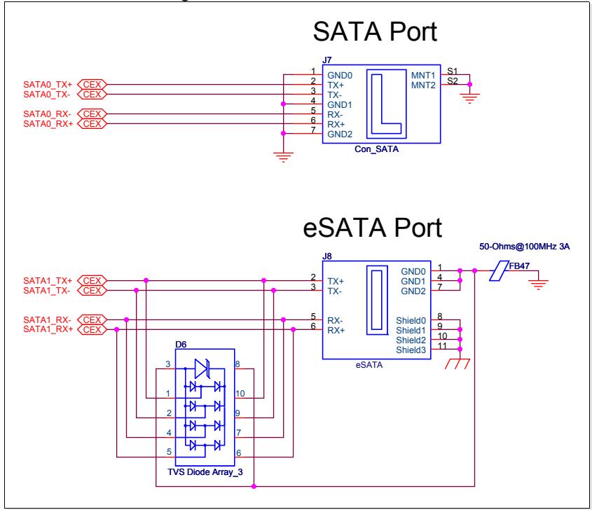
The following notes apply to Figure 33 above.
The Module provides a single LED signal SATA\_ACT# that can be used to indicate SATA drive activity.
The SATA connector shown is a Molex 67491 series, a 1.27mm-pitch 7-pin high-speed vertical plug.
The example design contains the SATA data and ground signals only. Power is provided through a separate connector from the system power supply. Alternate 22-pin connector types are available that deliver power and data to the SATA drive. This may be over a combined power/data cable or in a direct configuration in which the SATA drive mates directly to the 22-pin plug on the Carrier Board. Please refer to the SATA specification (Appendix G) for pin-out information.
ESD clamp diodes such as Semtech Rclamp0524 are shown in the eSATA schematic. This device contains low capacitance clamp diodes. The schematic shows two connections on each SATA signal to the clamp diodes. The second connection is actually a no-connect on the package and allows for straight-through routing for the SATA differential pairs.
Nets SATA0\_TX+/- through SATA1\_TX +/- are sourced from the COM Express Module SATA TX pins.
Nets SATA0\_RX+/- through SATA1\_RX +/- are sourced from SATA disks and are routed to the COM Express Module SATA RX pins.
Coupling capacitors are not needed on Carrier Board SATA lines. They are present on the COM Express Module.
# 2.10.3. Routing Considerations
Route SATA signals as differential pairs, with a 85 Ω differential impedance and a 50 Ω, singleended impedance. Ideally, a SATA pair is routed on a single layer adjacent to a ground plane. SATA pairs should not cross plane splits. Keep layer transitions to a minimum. SATA routing rules are also summarized in Section 6.5.8. 'Serial ATA Trace Routing Guidelines' on page 188.
As of the writing of this document, experience with SATA Gen3 implementations has shown that Carrier Board redrivers on the TX/RX pairs may be necessary. Check with your Module provider for further recommendations. Redrivers are available from vendors such as Texas Instruments, Pericom and others. The TI SN75LVCP600S is a redriver part in use by some Module vendors.
# 2.11. LVDS
# 2.11.1. Signal Definitions
The COM Express Specification provides an optional LVDS interface on the COM Express A-B connector. Module pins for two LVDS channels are defined and designated as LVDS\_A and LVDS\_B.
Systems use a single-channel LVDS for most displays. Dual LVDS channels are used for very high-bandwidth displays. Single-channel LVDS means that one complete RGB pixel is transmitted per display input clock (also known as the shift clock – see Table 27 'LVDS Signal Descriptions' below for a summary of LVDS terms). Dual-channel LVDS means that two complete RGB pixels are transmitted per display input clock. The two pixels are adjacent along a display line. Dual-channel LVDS does not mean that two LVDS displays can be driven.
Each COM Express LVDS channel consists of four differential data pairs and a differential clock pair for a total of five differential pairs per channel. COM Express Modules and Module chipsets may not use all pairs. For example, with 18-bit TFT displays, only three of the four data pairs on the LVDS\_A channel are used, along with the LVDS\_A clock. The LVDS\_B lines are not used. The manner in which RGB data is packed onto the LVDS pairs (including packing order and color depth) is not specified by the COM Express Specification. This may be Module-dependent. Further mapping details are given in Section 2.11.1.6. 'LVDS Display Color Mapping Tables' below.
There are five single-ended signals included to support the LVDS interface: two lines are used for an I2C interface that may be used to support EDID or other panel information and identification schemes. Additionally, there are an LVDS power enable (LVDS\_VDD\_EN) and backlight control and enable lines (LVDS\_BKLT\_CTRL and LVDS\_BKLT\_EN).
Table 27: LVDS Signal Descriptions
| Signal | Pin | Description | I/O | Comment |
| LVDS_A0+ | A71 | LVDS channel A differential signal pair 0 | O LVDS | |
| LVDS_A0- | A72 |
| LVDS_A1+ | A73 | LVDS channel A differential signal pair 1 | O LVDS | |
| LVDS_A1- | A74 |
| LVDS_A2+ | A75 | LVDS channel A differential signal pair 2 | O LVDS | |
| LVDS_A2- | A76 |
| LVDS_A3+ | A78 | LVDS channel A differential signal pair 3 | O LVDS | |
| LVDS_A3- | A79 |
| LVDS_A_CK+ | A81 | LVDS channel A differential clock pair | O LVDS | |
| LVDS_A_CK- | A82 |
| LVDS_B0+ | B71 | LVDS channel B differential signal pair 0 | O LVDS | |
| LVDS_B0- | B72 |
| LVDS_B1+ | B73 | LVDS channel B differential signal pair 1 | O LVDS | |
| LVDS_B1- | B74 |
| LVDS_B2+ | B75 | LVDS channel B differential signal pair 2 | O LVDS | |
| LVDS_B2- | B76 |
| LVDS_B3+ | B77 | LVDS channel B differential signal pair 3 | O LVDS | |
| LVDS_B3- | B78 |
| LVDS_B_CK+ | B81 | LVDS channel B differential clock pair | O LVDS | |
| LVDS_B_CK- | B82 |
| LVDS_VDD_EN | A77 | LVDS flat panel power enable. | O 3.3V, CMOS | |
| LVDS_BKLT_EN | B79 | LVDS flat panel backlight enable high active signal | O 3.3V, CMOS | |
| LVDS_BKLT_CTRL | B83 | LVDS flat panel backlight brightness control | O 3.3V, CMOS | |
| LVDS_I2C_CK | A83 | DDC I2C clock signal used for flat panel detection and control. | O 3.3V, CMOS | |
| LVDS_I2C_DAT | A84 | DDC I2C data signal used for flat panel detection and control. | I/O 3.3V, OD CMOS | |
# 2.11.1.1. Connector and Cable Considerations
When implementing LVDS signal pairs on a single-ended Carrier Board connector, the signals of a pair should be arranged so that the positive and negative signals are side by side. The trace lengths of the LVDS signal pairs between the COM Express Module and the connector on the Carrier Board should be the same as possible. Additionally, one or more ground traces/pins must be placed between the LVDS pairs.
Balanced cables (twisted pair) are usually better than unbalanced cables (ribbon cable) for noise reduction and signal quality. Balanced cables tend to generate less EMI due to field canceling effects and also tend to pick up electromagnetic radiation as common-mode noise, which is rejected by the receiver.
Twisted pair cables provide a low-cost solution with good balance and flexibility. They are capable of medium to long runs depending upon the application skew budget. A variety of shielding options are available.
Ribbon cables are a cost effective and easy solution. Even though they are not well suited for high-speed differential signaling they do work fine for very short runs. Most cables will work effectively for cable distances of <0.5m.
The cables and connectors that are to be utilized should have a differential impedance of 100Ω ±15%. They should not introduce major impedance discontinuities that cause signal reflections.
For more information about this subject, refer to the 'LVDS Owners Manual' available from Texas Instruments (http://www.ti.com).
# 2.11.1.2. Display Timing Configuration
The graphic controller needs to be configured to match the timing parameters of the attached flat panel display. To properly configure the controller, there needs to be some method to determine the display parameters. Different Module vendors provide differing ways to access display timing parameters. Some vendors store the data in non-volatile memory with the BIOS setup screen as the method for entering the data, other vendors might use a Module or Carrier based EEPROM. Some vendors might hard code the information into the BIOS, and other vendors might support panel located timing via the signals LVDS\_I2C\_CK and LVDS\_I2C\_DAT with an EEPROM strapped to 1010 000x. Regardless of the method used to store the panel timing parameters, the video BIOS will need to have the ability to access and decode the parameters. Given the number of variables it is recommended that Carrier designers contact Module suppliers to determine the recommend method to store and retrieve the display timing parameters.
The Video Electronics Standards Association (VESA) recently released DisplayID, a second generation display identification standard that can replace EDID and other proprietary methods for storing flat panel timing data. DisplayID defines a data structure which contains information such as display model, identification information, colorimetry, feature support, and supported timings and formats. The DisplayID data allows the video controller to be configured for optimal support for the attached display without user intervention. The basic data structure is a variable length block up to 256 bytes with additional 256 byte extensions as required. The DisplayID data is typically stored in a serial EPROM connected to the LVDS\_I2C bus. The EPROM can reside on the display or Carrier. DisplayID is not backwards compatible with EDID. Contact VESA (www.vesa.org) for more information.
# 2.11.1.3. Backlight Control
Backlight inverters are either voltage, PWM or resistor controlled. The COM Express specification provides two methods for controlling the brightness. One method is to use the backlight control and enable signals from the CPU chipset. These signals are brought on COM Express LVDS\_BKLT\_EN and LVDS\_BKLT\_CTRL. LVDS\_BKLT\_CTRL is a Pulse Width Modulated (PWM) output that can be connected to display inverters that accept a PWM input. The second method it to use the LVDS I2C bus to control an I2C DAC. The output of the DAC can be used to support voltage controlled inverters. The DAC can be used driving the backlight voltage control input pin of the inverter. The reference design shown in Figure 34 on page 97 below supports this. A header is used to allow the user to configure the type of backlight inverter signal used. In the example a DAC from Maxim is used ( MAX5362 http://www.maxim-ic.com).
# 2.11.1.4. Color Mapping and Terms
# FPD-Link and Open LDI Color Mapping
An LVDS stream consists of frames that pack seven data bits per LVDS frame. Details can be found in the tables below. The LVDS clock is one seventh of the source-data clock. The order in which panel data bits are packed into the LVDS stream is referred to as the LVDS color-mapping. There are two LVDS color-mappings in common use: FPD-Link and Open LDI. Open LDI is the newer standard.
The FPD-Link and Open LDI standards are the same for panels with color depths of 18 bits (6 Red, 6 Green, 6 Blue) or less. The 18 bits of color data and 3 bits of control data, or 21 bits total, are packed into 3 LVDS data streams. The LVDS clock is carried on a separate channel for a total of 4 LVDS pairs – 3 data pairs and a clock pair.
For 24-bit color depths, a 4th LVDS data pair is required (for a total of 5 LVDS pairs – 4 data and 1 clock). FPD-Link and Open LDI differ in this case. FPD-Link keeps the least significant color bits on the original 3 LVDS data pairs and adds the most significant color bits (the dominant or “most important” bits) to the 4th channel. Six bits are added: 2 Red, 2 Green, and 2 Blue (the seventh available bit slot in the 4th LVDS stream is not used).
A 24-bit, Open LDI implementation shifts the color bits on the original 3 LVDS data pairs up by two, such that the most significant color bits for both 18- and 24-bit panels occupy the same LVDS slots. For example, the most significant Red color bit is R5 for 18-bit panels and R7 for 24- bit panels. The 18-bit R5 and the 24-bit R7 occupy the same LVDS bit slot in Open LDI. The 4th LVDS data stream in Open LDI carries the least significant bits of a 24-bit panel – R0, R1, G0, G1, B0, and B1.
The advantage of Open LDI is that it provides an easier upgrade and downgrade path than FPD-Link does. An 18-bit panel can be used with an Open LDI 24-bit data stream by simply connecting the 1st three LVDS data pairs to the panel, and leaving the 4th LVDS data pair unused. This does not work with FPD-Link because the mapping for the 24-bit case is not compatible with the 18-bit case – the most significant data bits are on the 4th LVDS data stream.
If you design LVDS deserializers, work around the Module color-mapping by picking off the deserializer outputs in the order needed. If you use a flat panel with an integrated LVDS receiver, it is important that the displays color-mapping matches the Module’s color-mapping.
Table 28: LVDS Display Terms and Definitions
<table>| Term | Definition |
| Color-Mapping | Color-mapping refers to the order in which display color bits and control bits are placed into the serial LVDS stream. Each LVDS data frame can accept seven bits. The way in which the bits are serialized into the stream is arbitrary, as long as they are de-serialized in a corresponding way. Two main color-mapping schemes are FPD-Link and Open LDI. They are the same for 18-bit panels but differ for 24-bit panels. |
| DE | Display Enable – a control signal that asserts during an active display line. |
| Dual Channel | In a dual-channel bit stream, two complete RGB pixels are transmitted with each shift clock. The shift clock is one half the pixel frequency in this case. Dual channel LVDS streams are either 8 differential pairs (6 data pairs, 2 clock pairs, for dual 18 bit streams) or 10 differential pairs (8 data pairs, 2 clock pairs, for dual 24-bit streams). |
| Even Pixel | A pixel from an even column number, counting from 1. For example, on an 800x600 display, the even pixels along a row are in columns 2,4 ... 800. The odd pixels are in columns 1,3,5 ... 799. |
| FPD-Link | Flat Panel Display Link – an LVDS color-mapping scheme popularized by National Semiconductor. FPD Link color-mapping is the same as open LDI color-mapping for 18-bit displays but is different for 24-bit displays. FPD color-mapping puts the most significant bits of a 24-bit display onto the $4^{th}$ LVDS channel. |
| HSYNC | Horizontal Sync – a control signal that occurs once per horizontal display line. |
| LCLK | LVDS clock – the low voltage differential clock that accompanies the serialized LVDS data stream. For a single-channel LVDS stream, the LVDS clock is $1/7^{th}$ the pixel clock, which means there is one LVDS clock period for every 7 pixel clock periods. For a dual-channel LVDS data stream, the LVDS clock is $1/14^{th}$ the pixel clock, which means there is one LVDS clock period for every 14-pixel clock periods. |
| Odd Pixel | A pixel from an odd column number, counting from 1. For example, on an 800x600 display, the odd pixels along a row are in columns 1,3,5, ... 799. The even pixels are in columns 2,4 ...800. |
| Open LDI | Open LVDS Display Interface – a formalization by National Semiconductor of de facto LVDS standards. See Appendix G for a reference to the standard. Open LDI color-mapping is the same as FPD-Link color-mapping for 18-bit displays, but is different for 24-bit displays. Open LDI color-mapping puts the least significant bits of a 24-bit display onto the $4^{th}$ LVDS channel. Doing so means that an 18-bit display can operate on a 24-bit Open LDI link by using the first 3 LVDS data channels. |
| PCLK | Pixel clock – the clock associated with a single display pixel. For example, on a 640x480 display, there are 640 pixel clocks during the active display line period (and additional pixel clocks during the blanking periods). For a single-channel TFT display, the pixel clock is the same as the shift clock. For a dual-channel TFT display, the pixel clock is twice the frequency of the shift clock. |
| SCLK | Shift clock – the clock that shifts either a single pixel or a group of pixels into the display, depending on the display type. For a single-channel TFT display, the shift clock is the same as the pixel clock. For a dual-channel TFT display, the shift clock period is twice the pixel clock. For some display types, such as passive STN displays, the shift clock may be four- or eight-pixel clocks. |
| Single Channel | In a single-channel bit stream, a single RGB pixel is transmitted with each shift clock. The shift clock and the pixel clock are the same in this case. Single-channel LVDS streams are either 4 differential pairs (3 data pairs, 1 clock pair, for a single 18 bit stream) or 5 differential pairs (4 data pairs, 1 clock pair, for a single 24-bit stream). |
| Transmit Bit Order | The order, in time, in which bits are placed into the seven bit slots per LVDS frame. Bit 1 is earlier in time than bit 2, etc. |
| Unbalanced | Unbalanced means that the LVDS serializing hardware does not insert or manipulate bits to achieve a DC balance – i.e. an equal number of 0 and 1 bits, when averaged over multiple frames. |
| VSYNC | Vertical Sync – a control signal that occurs once per display frame. |
| Xmit Bit Order | See Transmit Bit Order. |
# 2.11.1.5. Note on Industry Terms
Some terms in this document that describe LVDS displays may vary from other documents (such as display data sheets from vendors, IC data sheets for graphics controllers and LVDS transmitters and receivers, the Open LDI specification, and COM Express Module documentation).
Examples of terms that may vary include:
For dual-channel displays, terms are needed to describe the adjacent pixels.
Various documents will reference for the same pair of pixels:
Odd and Even pixels (column count starts at 1)
Even and Odd pixels (column count starts at 0)
R10 and R20 for adjacent least significant Red bits
R00 and R10 for adjacent least significant Red bits
Terms used to describe the clocks vary:
The Open LDI specification uses the term “pixel clock” differently from most other documents. In the Open LDI specification, the “pixel clock” period is seven pixel periods long. Most other documents refer to this concept as the “LVDS clock.”
Transmit Bit Order
In this document, the seven bits in an LVDS frame are numbered 1 – 7, with Bit 1 being placed into the stream before Bit 2.
Display terms used in this document are defined in Table 28 above.
# 2.11.1.6. LVDS Display Color Mapping Tables
LVDS display color-mappings for single- and dual-channel displays are shown in Table 29 and Table 30 below.
For single-channel displays, COM Express Module LVDS B pairs are not used and may be left open. For single-channel, 18-bit displays, the LVDS\_A3± channel is not used and may be left open.
For 18-bit, single-channel and 36-bit, dual-channel displays, the FPD-Link and Open LDI colormappings are the same. For 24-bit, single-channel and 48-bit, dual-channel displays, mappings differ and care must be taken that the Module and display LVDS color-mappings agree.
Table 29: LVDS Display: Single Channel, Unbalanced Color-Mapping
| Xmit Bit Order | LVDS Clock | Open LDI 18 bit Single Ch | Open LDI 24 bit Single Ch | FPD Link 18 bit Single Ch | FPD Link 24 bit Single Ch |
| LVDS_A0± | 1 | 1 | G0 | G2 | G0 | G0 |
| 2 | 1 | R5 | R7 | R5 | R5 |
| 3 | 0 | R4 | R6 | R4 | R4 |
| 4 | 0 | R3 | R5 | R3 | R3 |
| 5 | 0 | R2 | R4 | R2 | R2 |
| 6 | 1 | R1 | R3 | R1 | R1 |
| 7 | 1 | R0 | R2 | R0 | R0 |
| LVDS_A1± | 1 | 1 | B1 | B3 | B1 | B1 |
| 2 | 1 | B0 | B2 | B0 | B0 |
| 3 | 0 | G5 | G7 | G5 | G5 |
| 4 | 0 | G4 | G6 | G4 | G4 |
| 5 | 0 | G3 | G5 | G3 | G3 |
| 6 | 1 | G2 | G4 | G2 | G2 |
| 7 | 1 | G1 | G3 | G1 | G1 |
| LVDS_A2± | 1 | 1 | DE | DE | DE | DE |
| 2 | 1 | VSYNC | VSYNC | VSYNC | VSYNC |
| 3 | 0 | HSYNC | HSYNC | HSYNC | HSYNC |
| 4 | 0 | B5 | B7 | B5 | B5 |
| 5 | 0 | B4 | B6 | B4 | B4 |
| 6 | 1 | B3 | B5 | B3 | B3 |
| 7 | 1 | B2 | B4 | B2 | B2 |
| LVDS_A3± | 1 | 1 | | | | |
| 2 | 1 | | B1 | | B7 |
| 3 | 0 | | B0 | | B6 |
| 4 | 0 | | G1 | | G7 |
| 5 | 0 | | G0 | | G6 |
| 6 | 1 | | R1 | | R7 |
| 7 | 1 | | R0 | | R6 |
| LVDS_A_CK± | | | LCLK = PCLK / 7SCLK = PCLK | LCLK= PCLK / 7SCLK = PCLK | LCLK = PCLK / 7SCLK = PCLK | LCLK = PCLK / 7SCLK = PCLK |
Table 30: LVDS Display: Dual Channel, Unbalanced Color-Mapping
| Xmit Bit Order | LVDS Clock | Open LDI 18 bit (36 bit) Dual Ch | Open LDI 24 bit (48 bit) Dual Ch | FPD Link 18 bit (36 bit) Dual Ch | FPD Link 24 bit (48 bit) Dual Ch |
| LVDS_A0± | 1 | 1 | Odd Pixel G0 | Odd Pixel G2 | Odd Pixel G0 | Odd Pixel G0 |
| 2 | 1 | Odd Pixel R5 | Odd Pixel R7 | Odd Pixel R5 | Odd Pixel R5 |
| 3 | 0 | Odd Pixel R4 | Odd Pixel R6 | Odd Pixel R4 | Odd Pixel R4 |
| 4 | 0 | Odd Pixel R3 | Odd Pixel R5 | Odd Pixel R3 | Odd Pixel R3 |
| 5 | 0 | Odd Pixel R2 | Odd Pixel R4 | Odd Pixel R2 | Odd Pixel R2 |
| 6 | 1 | Odd Pixel R1 | Odd Pixel R3 | Odd Pixel R1 | Odd Pixel R1 |
| 7 | 1 | Odd Pixel R0 | Odd Pixel R2 | Odd Pixel R0 | Odd Pixel R0 |
| LVDS_A1± | 1 | 1 | Odd Pixel B1 | Odd Pixel B3 | Odd Pixel B1 | Odd Pixel B1 |
| 2 | 1 | Odd Pixel B0 | Odd Pixel B2 | Odd Pixel B0 | Odd Pixel B0 |
| 3 | 0 | Odd Pixel G5 | Odd Pixel G7 | Odd Pixel G5 | Odd Pixel G5 |
| 4 | 0 | Odd Pixel G4 | Odd Pixel G6 | Odd Pixel G4 | Odd Pixel G4 |
| 5 | 0 | Odd Pixel G3 | Odd Pixel G5 | Odd Pixel G3 | Odd Pixel G3 |
| 6 | 1 | Odd Pixel G2 | Odd Pixel G4 | Odd Pixel G2 | Odd Pixel G2 |
| 7 | 1 | Odd Pixel G1 | Odd Pixel G3 | Odd Pixel G1 | Odd Pixel G1 |
| LVDS_A2± | 1 | 1 | DE | DE | DE | DE |
| 2 | 1 | VSYNC | VSYNC | VSYNC | VSYNC |
| 3 | 0 | HSYNC | HSYNC | HSYNC | HSYNC |
| 4 | 0 | Odd Pixel B5 | Odd Pixel B7 | Odd Pixel B5 | Odd Pixel B5 |
| 5 | 0 | Odd Pixel B4 | Odd Pixel B6 | Odd Pixel B4 | Odd Pixel B4 |
| 6 | 1 | Odd Pixel B3 | Odd Pixel B5 | Odd Pixel B3 | Odd Pixel B3 |
| 7 | 1 | Odd Pixel B2 | Odd Pixel B4 | Odd Pixel B2 | Odd Pixel B2 |
| LVDS_A3± | 1 | 1 | | | | |
| 2 | 1 | | Odd Pixel B1 | | Odd Pixel B7 |
| 3 | 0 | | Odd Pixel B0 | | Odd Pixel B6 |
| 4 | 0 | | Odd Pixel G1 | | Odd Pixel G7 |
| 5 | 0 | | Odd Pixel G0 | | Odd Pixel G6 |
| 6 | 1 | | Odd Pixel R1 | | Odd Pixel R7 |
| 7 | 1 | | Odd Pixel R0 | | Odd Pixel R6 |
| LVDS_A_CK± | | | LCLK= PCLK / 14SCLK = PCLK / 2 | LCLK = PCLK / 14SCLK = PCLK / 2 | LCLK = PCLK / 14SCLK = PCLK / 2 | LCLK = PCLK / 14SCLK = PCLK / 2 |
| LVDS_B0± | 1 | 1 | Even Pixel G0 | Even Pixel G2 | Even Pixel G0 | Even Pixel G0 |
| 2 | 1 | Even Pixel R5 | Even Pixel R7 | Even Pixel R5 | Even Pixel R5 |
| 3 | 0 | Even Pixel R4 | Even Pixel R6 | Even Pixel R4 | Even Pixel R4 |
| 4 | 0 | Even Pixel R3 | Even Pixel R5 | Even Pixel R3 | Even Pixel R3 |
| 5 | 0 | Even Pixel R2 | Even Pixel R4 | Even Pixel R2 | Even Pixel R2 |
| 6 | 1 | Even Pixel R1 | Even Pixel R3 | Even Pixel R1 | Even Pixel R1 |
| 7 | 1 | Even Pixel R0 | Even Pixel R2 | Even Pixel R0 | Even Pixel R0 |
| LVDS_B1± | 1 | 1 | Even Pixel B1 | Even Pixel B3 | Even Pixel B1 | Even Pixel B1 |
| 2 | 1 | Even Pixel B0 | Even Pixel B2 | Even Pixel B0 | Even Pixel B0 |
| 3 | 0 | Even Pixel G5 | Even Pixel G7 | Even Pixel G5 | Even Pixel G5 |
| 4 | 0 | Even Pixel G4 | Even Pixel G6 | Even Pixel G4 | Even Pixel G4 |
| 5 | 0 | Even Pixel G3 | Even Pixel G5 | Even Pixel G3 | Even Pixel G3 |
| 6 | 1 | Even Pixel G2 | Even Pixel G4 | Even Pixel G2 | Even Pixel G2 |
| 7 | 1 | Even Pixel G1 | Even Pixel G3 | Even Pixel G1 | Even Pixel G1 |
| LVDS_B2± | 1 | 1 | | | | |
| 2 | 1 | | | | |
| 3 | 0 | | | | |
| 4 | 0 | Even Pixel B5 | Even Pixel B7 | Even Pixel B5 | Even Pixel B5 |
| 5 | 0 | Even Pixel B4 | Even Pixel B6 | Even Pixel B4 | Even Pixel B4 |
| 6 | 1 | Even Pixel B3 | Even Pixel B5 | Even Pixel B3 | Even Pixel B3 |
| 7 | 1 | Even Pixel B2 | Even Pixel B4 | Even Pixel B2 | Even Pixel B2 |
| LVDS_B3± | 1 | 1 | | | | |
| 2 | 1 | | Even Pixel B1 | | Even Pixel B7 |
| 3 | 0 | | Even Pixel B0 | | Even Pixel B6 |
| 4 | 0 | | Even Pixel G1 | | Even Pixel G7 |
| 5 | 0 | | Even Pixel G0 | | Even Pixel G6 |
| 6 | 1 | | Even Pixel R1 | | Even Pixel R7 |
| 7 | 1 | | Even Pixel R0 | | Even Pixel R6 |
| LVDS_B_CK± | | | LCLK= PCLK / 14SCLK = PCLK / 2 | LCLK = PCLK / 14SCLK = PCLK / 2 | LCLK = PCLK / 14SCLK = PCLK / 2 | LCLK = PCLK / 14SCLK = PCLK / 2 |
# 2.11.2. Reference Schematics
Figure 34: LVDS Reference Schematic
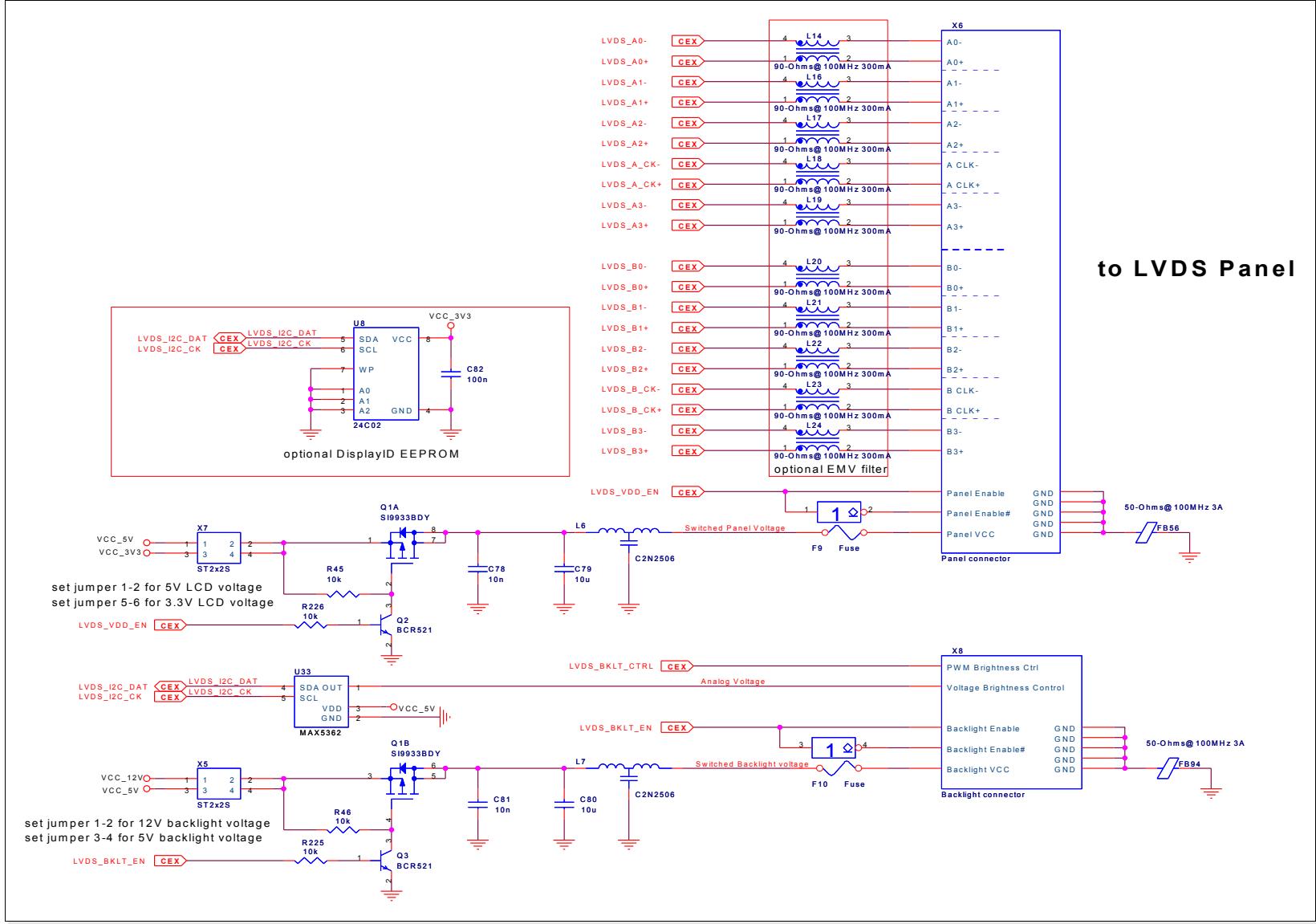
# 2.11.3. Routing Considerations
Route LVDS signals as differential pairs (excluding the five single-ended support signals), with a 100-Ω differential impedance and a 55-Ω, single-ended impedance. Ideally, a LVDS pair is routed on a single layer adjacent to a ground plane. LVDS pairs should not cross plane splits. Keep layer transitions to a minimum. Reference LVDS pairs to a power plane if necessary. The power plane should be well-bypassed.
Length-matching between the two lines that make up an LVDS pair (“intra-pair”) and between different LVDS pairs (“inter-pair”) is required. Intra-pair matching is tighter than the inter-pair matching.
All LVDS pairs should have the same environment, including the same reference plane and the same number of vias.
LVDS routing rules are summarized in 6.5.9. 'LVDS Trace Routing Guidelines' on page 189 below.
# 2.12. Embedded DisplayPort (eDP)
Embedded DisplayPort (eDP) is a digital display interface standard produced by the Video Electronics Standards Association (VESA) for digital interconnect of Audio and Video.
Embedded DisplayPort defines a standardized display panel interface for internal connections; e.g., graphics interfaces to notebook display panels. It supports advanced power-saving features including seamless refresh rate switching, display panel and backlight control protocol that works through the AUX channel, and Panel Self-Refresh (PSR) feature developed to save system power and further extend battery life in portable PC systems. PSR mode allows the GPU to enter power saving states in between frame updates by including framebuffer memory in the display panel controller.
Embedded DisplayPort is intended to replace LVDS as the interface to flat panel displays integrated into a product. Unlike DisplayPort, embedded DisplayPort does not define a specific connector or pin-out. The COM Express specification shares the LVDS pins with embedded DisplayPort.
# 2.12.1. Signal Definitions
eDP is available in Type 6 and type 10 pin-outs as an alternative to the LVDS A channel. The Module can provide LVDS only, eDP only or Dual-Mode for both interfaces. Please refer to relevant Module documentation for the supported interfaces.
Table 31: eDP Signal Description
| Signal | Pins T6/T10 | Description | I/O |
| eDP_TX0+ | A75 | eDP lane 0, TX + | O PCIe |
| eDP_TX0- | A76 | eDP lane 0, TX - | O PCIe |
| eDP_TX1+ | A73 | eDP lane 1, TX + | O PCIe |
| eDP_TX1- | A74 | eDP lane 1, TX - | O PCIe |
| eDP_TX2+ | A71 | eDP lane 2, TX + | O PCIe |
| eDP_TX2- | A72 | eDP lane 2, TX - | O PCIe |
| eDP_TX3+ | A81 | eDP lane 3, TX + | O PCIe |
| eDP_TX3- | A82 | eDP lane 3, TX - | O PCIe |
| eDP_VDD_EN | A77 | eDP power enable | O CMOS |
| eDP_BLKT_EN | B79 | eDP backlight enable | O CMOS |
| eDP_BLKT_CTRL | B83 | EDP backlight brightness control | O CMOS |
| eDP_AUX+ | A83 | eDP auxiliary lane + | I/O PCIe |
| eDP_AUX- | A84 | eDP auxiliary lane - | I/O PCIe |
| eDP_HPD | A87 | Detection of Hot Plug / Unplug and notification of the link layer | I CMOS |
# 2.12.2. Reference Schematics
Figure 35: eDP Reference Schematic
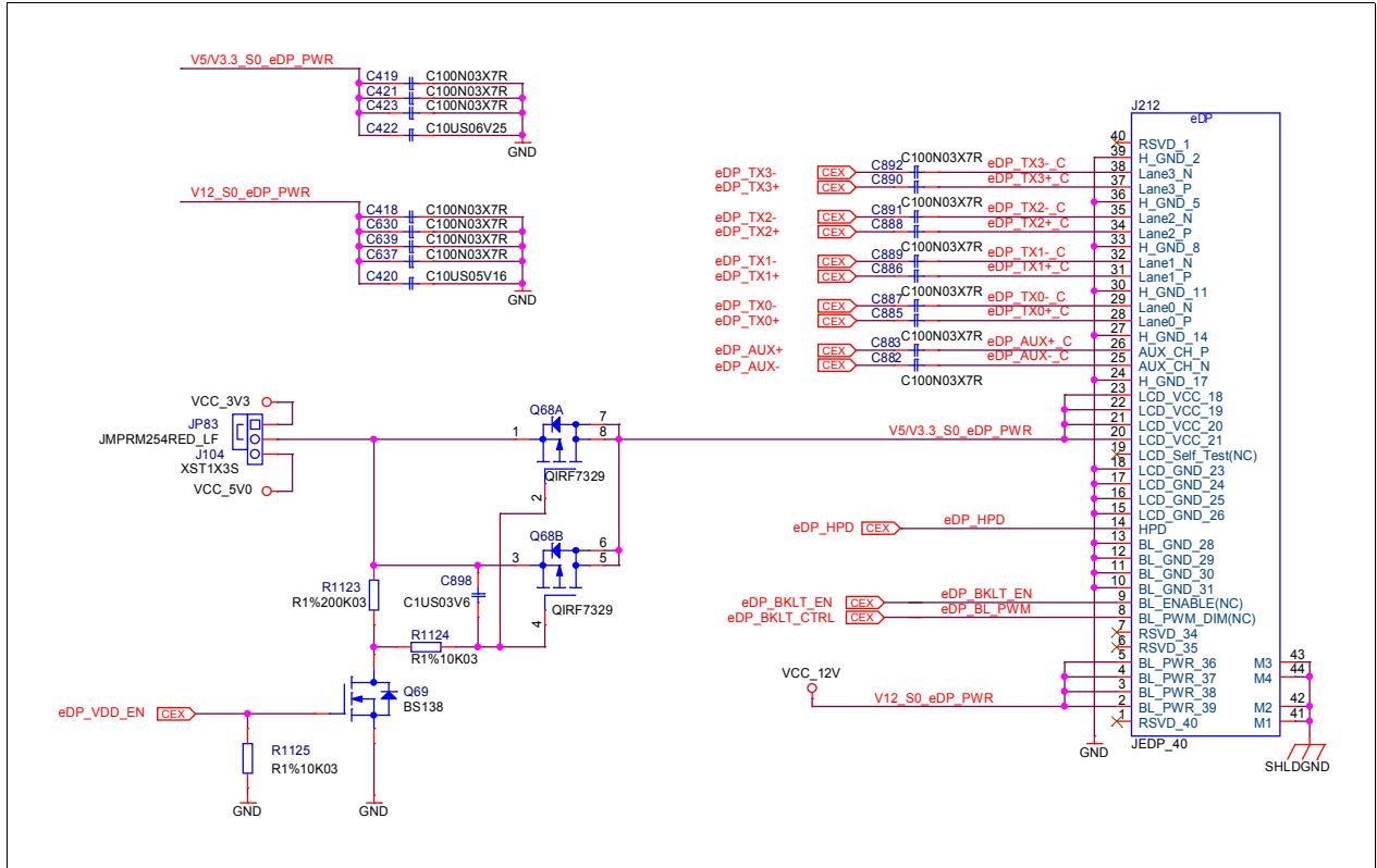
The reference schematic provides a generic eDP interface. The eDP connector used in the design is an example only. Other connectors can be used based on the design requirements. JP83 selects 3.3 or 5V for the panel power. R1125 ensures that panel power is disabled when the Module is powering up and before the signal is actively driven. The panel control signals eDP\_BKLT\_EN, eDP\_BKLT\_CTRL as well as eDP\_HPD are 3.3V level signals, check your panel specifications for correct voltage levels and provide translation if necessary. The reference design supports individual backlight control signals. It should be noted that some panels handle these functions over the AUX channel.
# 2.12.3. Routing Considerations
The traces from JP83 and associated FETs to the eDP connector carry power to the panel. The traces should be routed with appropriate thickness to handle the current expected.
eDP\_TX and eDP\_AUX differential pairs should be routed as high speed differential pairs.
The panel control signals are low speed and do not require any additional care.
# 2.13. VGA
# 2.13.1. Signal Definitions
The COM Express Specification defines an analog VGA RGB interface for all Module types, except type 10. The interface consists of three analog color signals (Red, Green, Blue); digital Horizontal and Vertical Sync signals as well as a dedicated I2C bus for Display Data Control (DDC) implementation for monitor capability identification. The corresponding signals can be found on the COM Express Module connector row B.
Table 32: VGA Signal Description
| Signal | Pin | HDSUB15 | Description | I/O | Comment |
| VGA_RED | B89 | 1 | Red component of analog DAC monitor output, designed to drive a 37.5Ω equivalent load. | O Analog | Analog output |
| VGA_GRN | B91 | 2 | Green component of analog DAC monitor output, designed to drive a 37.5Ω equivalent load. | O Analog | Analog output |
| VGA_BLU | B92 | 3 | Blue component of analog DAC monitor output, designed to drive a 37.5Ω equivalent load. | O Analog | Analog output |
| VGA_HSYNC | B93 | 13 | Horizontal sync output to VGA monitor. | O 3.3V CMOS | |
| VGA_VSYNC | B94 | 14 | Vertical sync output to VGA monitor. | O 3.3V CMOS | |
| VGA_I2C_CK | B95 | 15 | DDC clock line (I2C port dedicated to identify VGA monitor capabilities). | O 3.3V CMOS | Level shifter might be necessary |
| VGA_I2C_DAT | B96 | 12 | DDC data line. | I/O 3.3V CMOS | Level shifter might be necessary |
| GND | | 5..8, 10 | Analog and Digital GND | | |
| DDC_POWER | | 9 | 5V DDC supply voltage for monitor EEPROM | | Power |
| N.C. | | 4, 11 | Not Connected | | |
# 2.13.2. VGA Connector
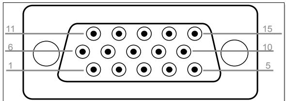
Figure 36: Female VGA Connector HDSUB15 for Carrier Board
# 2.13.3. VGA Reference Schematics
This reference schematic shows a circuitry implementing a VGA port.
Figure 37: VGA Reference Schematics
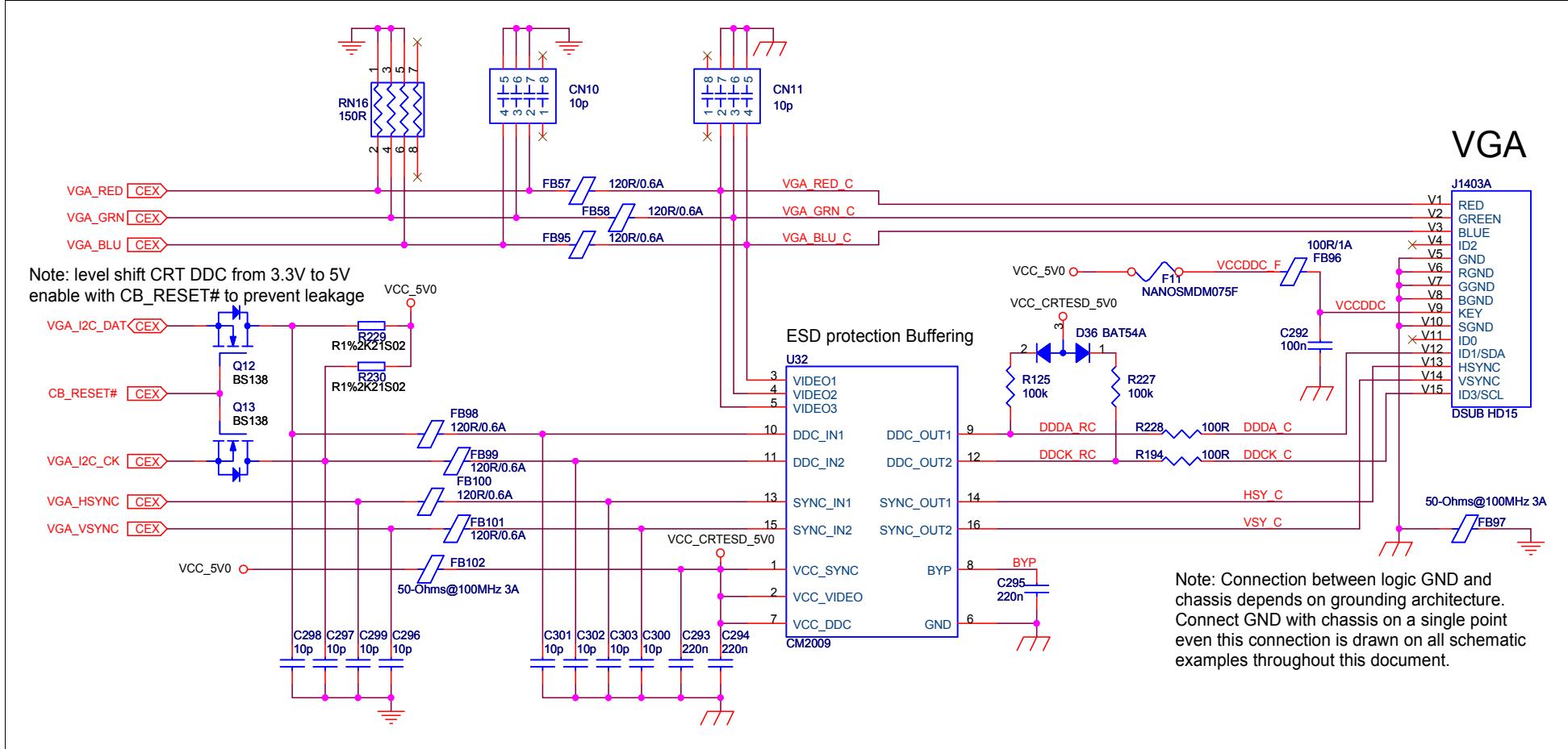
# 2.13.4. Routing Considerations
# 2.13.4.1. RGB Analog Signals
The RGB signal interface of the COM Express Module consists of three identical 8-bit digital-toanalog converter (DAC) channels. One each for the red, green, and blue components of the monitor signal. Each of these channels should have a 150Ω ±1% pull-down resistor connected from the DAC output to the Carrier Board ground. A second 150Ω ±1% termination resistor exists on the COM Express Module itself. An additional 75Ω termination resistor exists within the monitor for each analog DAC output signal.
Since the DAC runs at speeds up to 350MHz, special attention should be paid to signal integrity and EMI. There should be a PI-filter placed on each RGB signal that is used to reduce highfrequency noise and EMI. The PI-filter consists of two 10pF capacitors with a 120Ω @ 100MHz ferrite bead between them. It is recommended to place the PI-filters and the terminating resistors as close as possible to the standard VGA connector.
# 2.13.4.2. HSYNC and VSYNC Signals
The horizontal and vertical sync signals 'VGA\_HSYNC' and 'VGA\_VSYNC' provided by the COM Express Module are 3.3V tolerant outputs. Since VGA monitors may drive the monitor sync signals with 5V tolerance, it is necessary to implement high impedance unidirectional buffers. These buffers prevent potential electrical over-stress of the Module and avoid that VGA monitors may attempt to drive the monitor sync signals back to the Module.
For optimal ESD protection, additional low capacitance clamp diodes should be implemented on the monitor sync signals. They should be placed between the 5V power plane and ground and as close as possible to the VGA connector.
# 2.13.4.3. DDC Interface
COM Express provides a dedicated I2C bus for the VGA interface. It corresponds to the VESA™ defined DDC interface that is used to read out the CRT monitor specific Extended Display Identification Data (EDID™). The appropriate signals 'VGA\_I2C\_DAT' and 'VGA\_I2C\_CK' of the COM Express Module are supposed to be 3.3V tolerant. Since most VGA monitors drive the internal EDID™ EEPROM with a supply voltage of 5V, the DDC interface on the VGA connector must also be sourced with 5V. This can be accomplished by placing a 100kΩ pull-up resistors between the 5V power plane and each DDC interface line. Level shifters for the DDC interface signals are required between the COM Express Module signal side and the signals on the standard VGA connector on the Carrier Board.
Additional Schottky diodes must be placed between 5V and the pull-up resistors of the DDC signals to avoid backward current leakage during Suspend operation of the Module.
# 2.13.4.4. ESD Protection/EMI
All VGA signals need ESD protection and EMI filters. This can be provided by using a VGA port companion circuit or similar protective components. The Carrier Board sample VGA schematic shown above uses a “VGA companion” protection circuit, the CM2009 from California Micro Devices. The companion circuit implements ESD protection for the analog DAC output, DDC and SYNC signals through the use of low-capacitance current steering diodes. Additionally, it incorporates level shifting for the DDC signals and buffering for the SYNC signals. For more details, refer to the 'CM2009' data sheet.
Many other protection and level shifting solutions are possible. Semtech offers a wide variety of low capacitance ESD suppression parts suitable for high speed signals. One such Semtech part is the RCLAMP502B.
# 2.14. TV-Out
TV-Out signals have been removed in COM.0 Rev. 2.0 and the former content of this chapter can still be found in the section Appendix A: Deprecated Features on page 203
# 2.15. Digital Audio Interfaces
The COM Express Specification allocates seven pins on the A-B connector to support digital AC’97 and HD interfaces to audio Codecs on the Carrier Board. The pins are available on all Module types. High-definition (HD) audio uses the same digital-signal interface as AC ’97 audio. Codecs for AC ’97 and HD Audio are different and not compatible. Current Module chipsets support HD Audio only.
Signal Definitions
Table 33: Audio Codec Signal Descriptions
| Signal | Pin | Description | I/O | Comment |
| AC/HDA_RST# | A30 | CODEC Reset. | O 3.3VSuspendCMOS | |
| AC/HDA_SYNC | A29 | Serial Sample Rate Synchronization. | O 3.3VCMOS | |
| AC/HDA_BITCLK | A32 | 24 MHz Serial Bit Clock for HDA CODEC. | O 3.3VCMOS | |
| AC/HDA_SDOUT | A33 | Audio Serial Data Output Stream. | O 3.3VCMOS | |
| AC/HDA_SDIN0 | B30 | Audio Serial Data Input Stream from CODEC[0:2]. | I 3.3VSuspendCMOS | |
| AC/HDA_SDIN1 | B29 |
| AC/HDA_SDIN2 | B28 |
The codec on a COM Express Carrier Board is usually connected as the primary codec with the codec ID 00 using the data input line 'AC/HDA\_SDIN0'. Up to two additional codecs with ID 01 and ID 10 can be connected to the COM Express Module by using the other designated signals 'AC/HDA\_SDIN1' and 'AC/HDA\_SDIN2'.
Connect the primary audio codec to the serial data input signal 'AC/HDA\_SDIN0' and ensure that the corresponding bit clock input signal 'AC/HDA\_BITCLK' is connected to the AC'97/HDA interface of the COM Express Module.
Clocking over the signal 'AC/HDA\_BITCLK' is derived from a 24.576 MHz crystal or crystal oscillator provided by the primary codec in AC97 implementations. The crystal is not required in HDA implementations. This clock also drives the second and the third audio codec if more than one codec is used in the application. For crystal or crystal oscillator requirements, refer to the datasheet of the primary codec.
Figure 38: Multiple Audio Codec Configuration
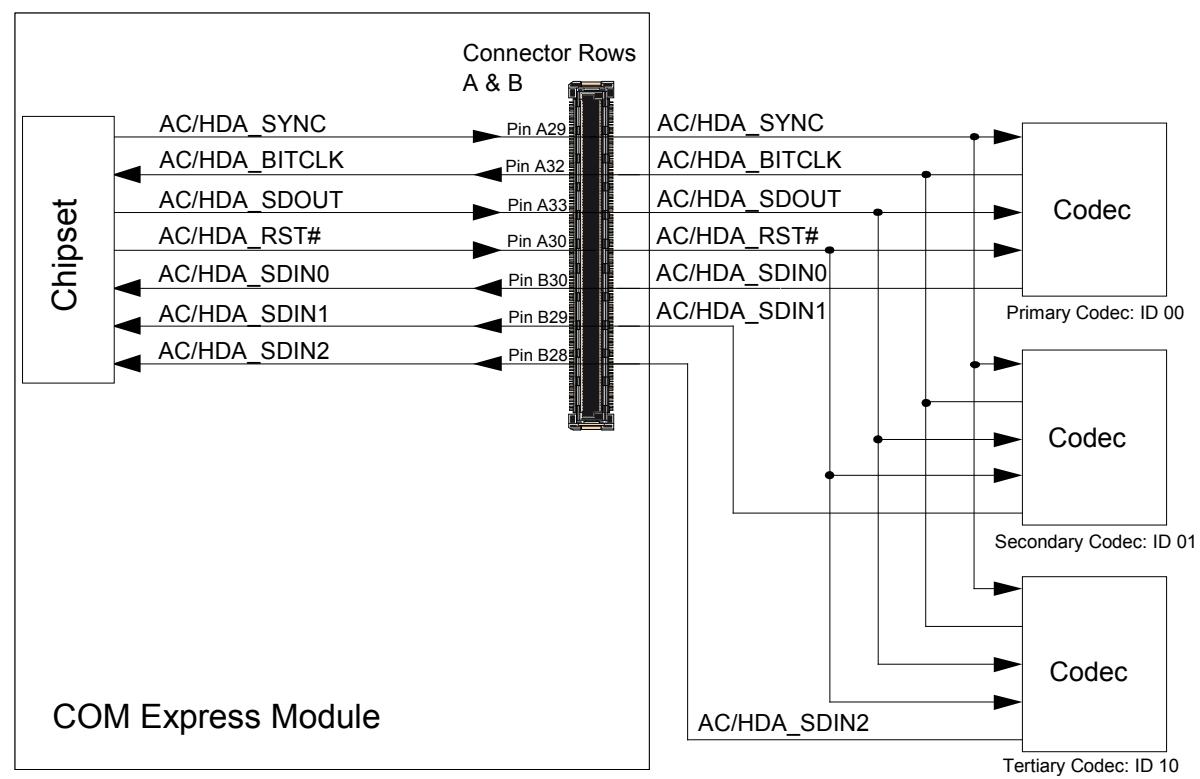
# 2.15.1. Reference Schematics
# 2.15.1.1. High Definition Audio
Figure 39: HDA Example Schematic
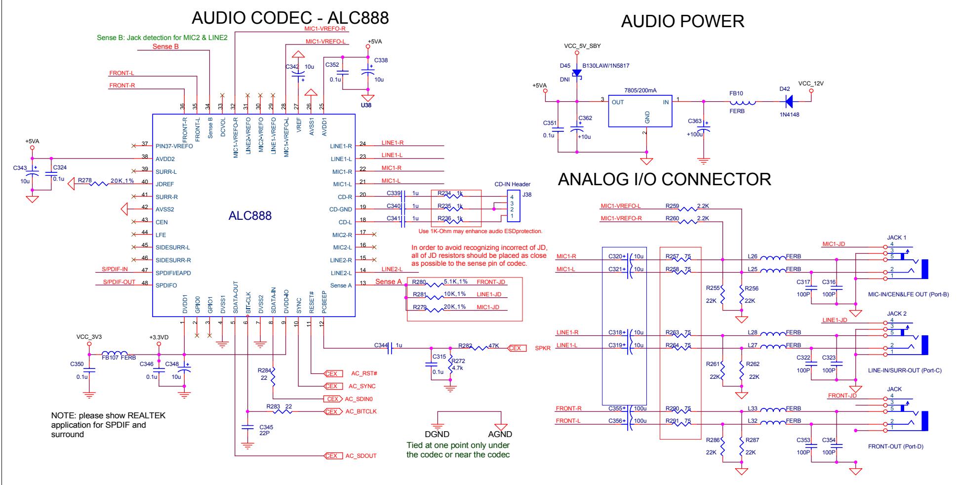
# 2.15.1.2. AC'97
Figure 40: AC'97 Schematic Example
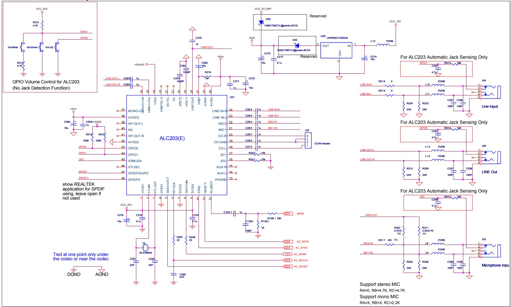
Figure 41: Audio Amplifier
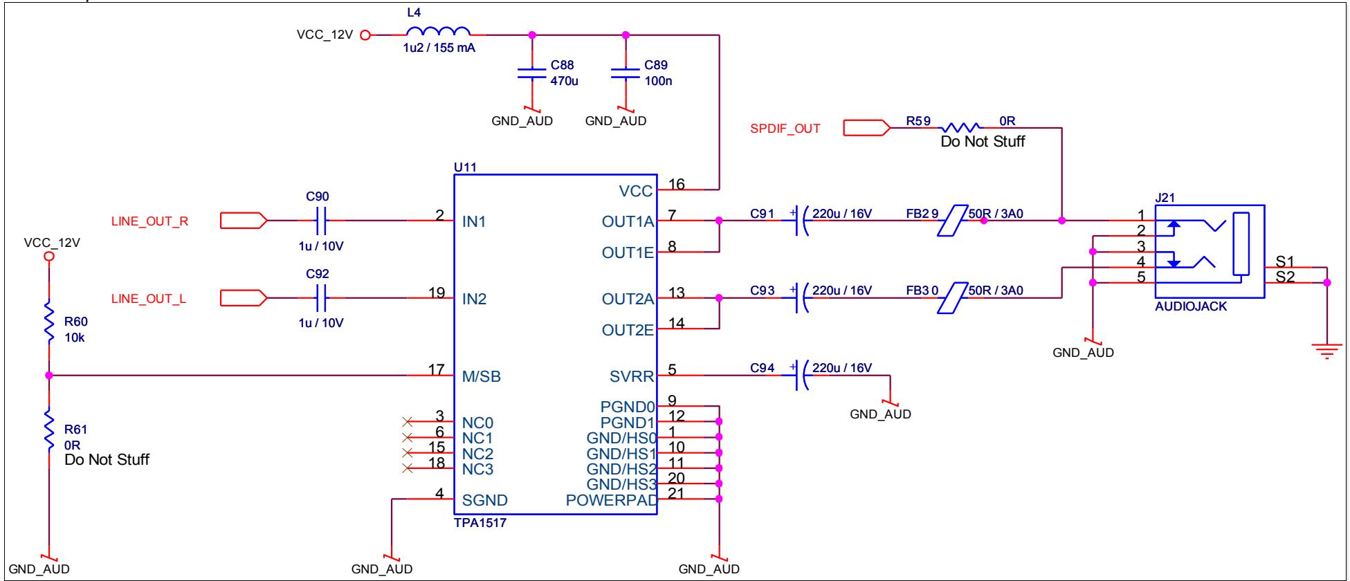
The example above shows a traditional class AB amplifier. There are many physically smaller and more power efficient class D audio amplifier options from vendors such as Texas Instruments, NXP and others.
# 2.15.1.3. Routing Considerations
The implementation of proper component placement and routing techniques will help to ensure that the maximum performance available from the codec is achieved. Routing techniques that should be observed include properly isolating the codec, associated audio circuitry, analog power supplies and analog ground planes from the rest of the Carrier Board. This includes split planes and the proper routing of signals not associated with the audio section.
The following is a list of basic recommendations:
Traces must be routed with a target impedance of 55Ω with an allowed tolerance of ±15%.
Ground return paths for the analog signals must be given special consideration.
Digital signals routed in the vicinity of the analog audio signals must not cross the power plane split lines. Locate the analog and digital signals as far as possible from each other.
Partition the Carrier Board with all analog components grouped together in one area and all digital components in another.
Keep digital signal traces, especially the clock, as far as possible from the analog input and voltage reference pins.
Provide separate analog and digital ground planes with the digital components over the digital ground plane, and the analog components, including the analog power regulators, over the analog ground plane. The split between the planes must be a minimum of 0.05 inch wide.
Route analog power and signal traces over the analog ground plane.
Route digital power and signal traces over the digital ground plane.
Position the bypassing and decoupling capacitors close to the IC pins with wide traces to reduce impedance.
Place the crystal or oscillator (depending on the codec used) as close as possible to the codec. (HDA implementations generally do not require a crystal at the codec)
Do not completely isolate the analog/audio ground plane from the rest of the Carrier Board ground plane. Provide a single point (0.25 inch to 0.5 inch wide) where the analog/isolated ground plane connects to the main ground plane. The split between the planes must be a minimum of 0.05 inch wide.
Any signals entering or leaving the analog area must cross the ground split in the area where the analog ground is attached to the main Carrier Board ground. That is, no signal should cross the split/gap between the ground planes, because this would cause a ground loop, which in turn would greatly increase EMI emissions and degrade the analog and digital signal quality.
# 2.16. LPC Bus – Low Pin Count Interface
Since COM Express is designed to be a legacy free standard for embedded Modules, it does not support legacy functionality on the Module, such as PS/2 keyboard/mouse, serial ports, and parallel ports. Instead, it provides an LPC interface that can be used to add peripheral devices to the Carrier Board design. COM Express also provides interface pins necessary for (optional) Carrier Board resident PS keyboard controllers
The Low Pin Count Interface was defined by the Intel® Corporation to facilitate the industry's transition toward legacy free systems. It allows the integration of low-bandwidth legacy I/O components within the system, which are typically provided by a Super I/O controller.
Furthermore, it can be used to interface Firmware Hubs, Trusted Platform Module (TPM) devices, general-purpose inputs and outputs, and Embedded Controller solutions. Data transfer on the LPC bus is implemented over a 4 bit serialized data interface, which uses a 33MHz LPC bus clock. It is straightforward to develop PLDs or FPGAs that interface to the LPC bus. A PLD circuit example is given in Figure 43 'LPC PLD Example – Port 80 Decoder Schematic' below.
For more information about LPC bus, refer to the 'Intel® Low Pin Count Interface Specification Revision 1.1'.
# 2.16.1. Signal Definition
Table 34: LPC Interface Signal Descriptions
| Signal | Pin | Description | I/O | Comment |
| LPC_SERIRQ | A50 | LPC serialized IRQ. | I/O 3.3V CMOS | |
| LPC_FRAME# | B3 | LPC frame indicates start of a new cycle or termination of a broken cycle. | O 3.3V CMOS | |
| LPC_AD0 | B4 | LPC multiplexed command, address and data. | I/O 3.3V CMOS | |
| LPC_AD1 | B5 |
| LPC_AD2 | B6 |
| LPC_AD3 | B7 |
| LPC_DRQ0# | B8 | LPC encoded DMA/Bus master request. | I 3.3V CMOS | Not all Modules support LPC DMA. Contact your vendor for information. |
| LPC_DRQ1# | B9 |
| LPC_CLK | B10 | LPC clock output 33MHz. | O 3.3V CMOS | |
Note Implementing external LPC devices on the COM Express Carrier Board always requires customization of the COM Express Module's BIOS in order to support basic initialization for those LPC devices. Otherwise the functionality of the LPC devices will not be supported by a Plug&Play or ACPI capable system. See Section 4 'BIOS Considerations' on page 170 below for further information. Contact your Module vendor for a list of specific SIO devices for which there may be BIOS support.
# 2.16.2. LPC Bus Reference Schematics
# 2.16.2.1. LPC Bus Clock Signal
COM Express specifies a single LPC reference clock signal called 'LPC\_CLK' on the Modules connector at row B pin B10. Newer chipsets do not provide a free running LPC\_CLK. The clock is stopped and started on-the-fly. The clock is only active during LPC bus cycles. This kind of a clock can cause problems when used with PLL based zero delay buffers which require a number of clock cycles to lock onto the incoming clock before the output is active. The issue is that the LPC\_CLK is not active for enough cycles before the data is read/written to the LPC bus. The result is that the target LPC device does not see an LPC\_CLK and misses the LPC cycle.
Carrier designers should not buffer LPC\_CLK for maximum Module interoperability. The COM Express specification intends for a single load on the clock but experience has shown that two devices can be driven if both devices are within 2" of each other.
# 2.16.2.2. LPC Reset Signal
The LPC interface should use the signal 'CB\_RESET#' as its reset input. This signal is issued by the COM Express Module as a result of a low 'SYS\_RESET#', a low 'PWR\_OK' or a watchdog timeout event. If there are multiple LPC devices implemented on the Carrier Board, it is recommended to split the signal 'CB\_RESET#' so that each LPC device will be provided with a separate reset signal. Therefore a buffer circuit like the one shown in Figure 42 below should be used.
Figure 42: LPC Reset Buffer Reference Circuitry
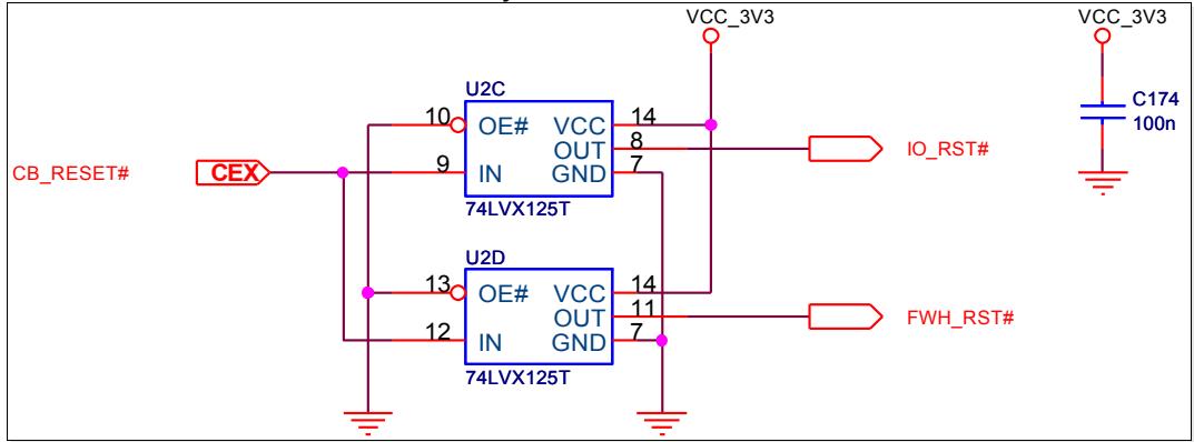
Note: The LPC Firmware Hub section has been moved to section 9 'Appendix A: Deprecated Features' on page 203 below in this version of the Carrier Design Guide. LPC Firmware hubs were typically used for Carrier based BIOS in previous generation designs. A Carrier based BIOS is now typically support on SPI. See section 2.17 'SPI – Serial Peripheral Interface Bus' on page 118 below for more information.
# 2.16.2.3. LPC PLD Example – Port 80 Decoder
Figure 43: LPC PLD Example – Port 80 Decoder Schematic
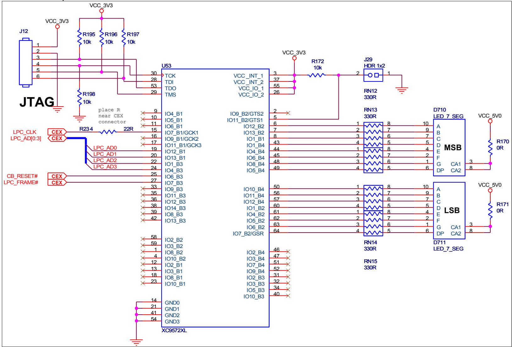
The following applies to Figure 43 above.
The JTAG header may be used to program the PLD in-circuit.
The LPC bus is the interface to the Module host system.
Two seven-segment LED displays show the Port 80 POST (Power On Self Test) codes.
PLD outputs drive the LEDs.
On some systems, a BIOS setting is needed to allow POST codes to be forwarded to the LPC bus.
Warning: Note that the pins on this particular CPLD are 5V tolerant and some of the pins are subjected to voltages near 5V through the 7 segment LED.
# 2.16.2.4. SuperIO
Figure 44: LPC Super I/O Example
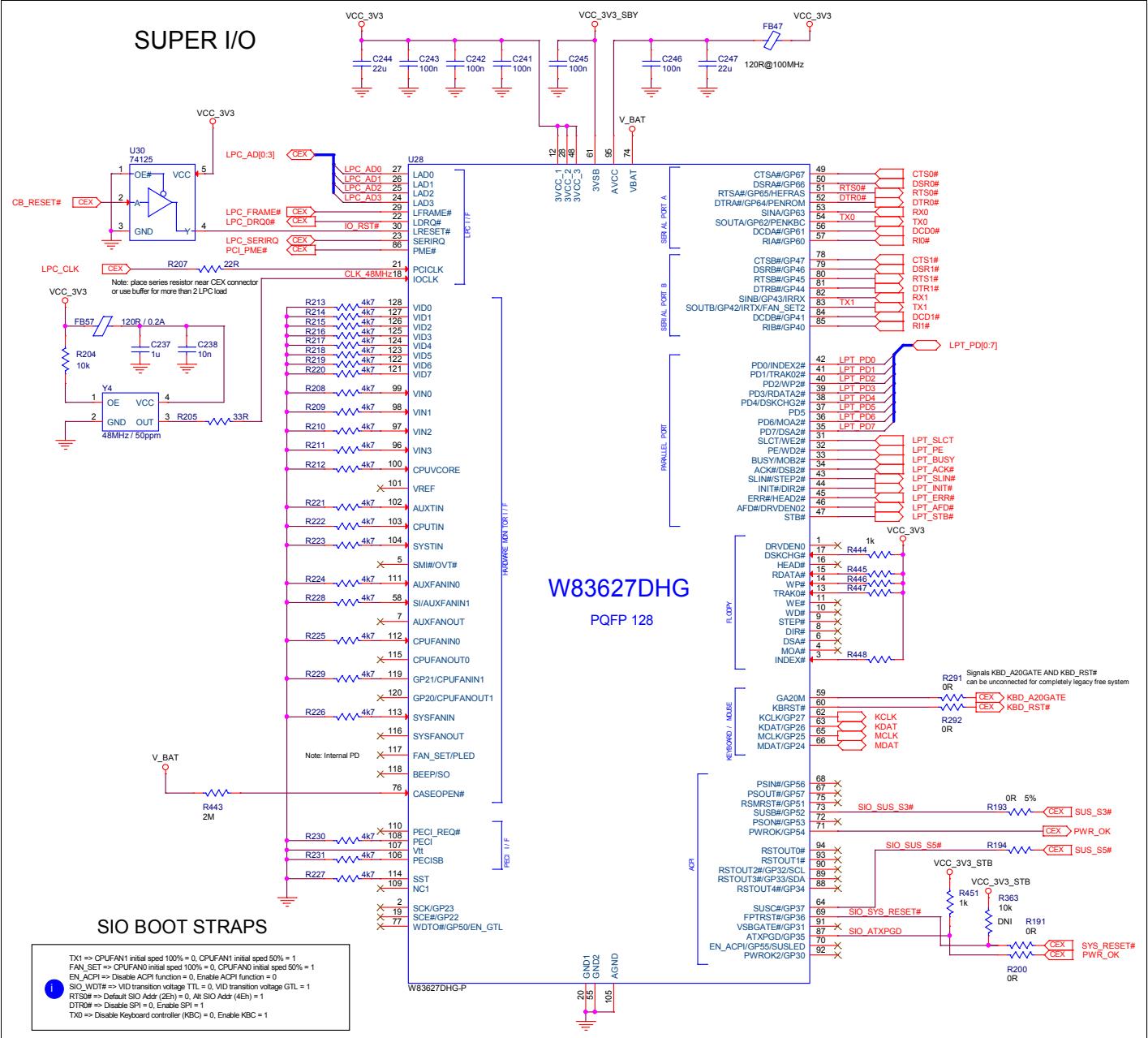
Figure 45: LPC Serial Interfaces
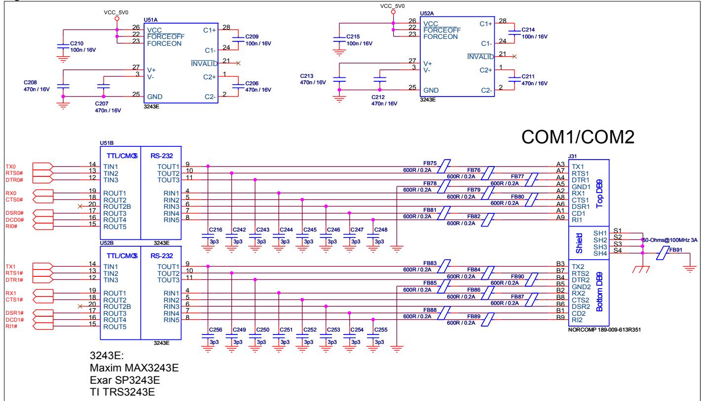
Note: Connection between logic GND and chassis depends on grounding architecture. Connect GND with chassis at a single point even though this connection is drawn on all schematic examples throughout this document.
# 2.16.3. Routing Considerations
# 2.16.3.1. General Signals
LPC signals are similar to PCI signals and may be treated similarly. Route the LPC bus as 55 Ω, single-ended signals. The bus may be referenced to ground (preferred), or to a well-bypassed power plane or a combination of the two. Point-to-point (daisy-chain) routing is preferred, although stubs up to 1.5 inches may be acceptable. Length-matching among LPC\_AD[3:0], LPC\_FRAME# are needed
See Section 6.6.3 'LPC Trace Routing Guidelines' on page 193 below.
# 2.16.3.2. Bus Clock Routing
The LPC bus clock is similar to the PCI bus clock and should be treated similarly. The COM Express Specification allows 1.6 ns +/- 0.1ns for the propagation delay of the LPC clock from the Module pin to the LPC device destination pin. Using a typical propagation delay value of 180 ps / inch, this works out to 8.88 inches of Carrier Board trace for a device-down application. For device-up situations, 2.5 inches of clock trace are assumed to be on the LPC slot card (by analogy to the PCI specification). This is deducted from the 8.88 inches, yielding 6.38 inches.
On a Carrier Board with a small form factor, serpentine clock traces may be required to meet the clock-length requirement.
Route the LPC clock as a single-ended, 55 Ω trace with generous clearance to other traces and to itself. A continuous ground-plane reference is recommended. Routing the clock on a single ground referenced internal layer is preferred to reduce EMI.
The LPC clock implementation should follow the routing guidelines for the PCI clock defined in the COM Express specification and the 'PCI Local Bus Specification Revision 2.3'. In addition to this refer to Section 6.6.1 'PCI Trace Routing Guidelines' on page 191 below.
# 2.17. SPI – Serial Peripheral Interface Bus
The SPI interface is defined in this specification to service as an off-module option for BIOS storage. The SPI interface replaces the LPC Firmware Hub interface, which is now considered a legacy interface for firmware storage (LPC does continue to be used for SuperIO connectivity). Many current chipsets only specify SPI for BIOS/Firmware storage usage, so the COM.0 specification is limited to that connectivity use-case to enable maximum compatibility across Modules and silicon platforms. Additional features, such as SPI-based Trusted Platform Module support might be added to a given carrier design, but compatibility is not guaranteed across Modules.
# 2.17.1. Signal Definition
Table 35: SPI Signal Definition
| Signal | Pin | Description | I/O |
| SPI_CS# | B97 | Chip select for Carrier Board SPI – may be sourced from chipset SPI0 or SPI1 | O CMOS – 3.3V Suspend |
| SPI_MISO | A92 | Data in to Module from Carrier SPI | I CMOS – 3.3V Suspend |
| SPI_MOSI | A95 | Data out from Module to Carrier SPI | O CMOS – 3.3V Suspend |
| SPI_CLK | A94 | Clock from Module to Carrier SPI | O CMOS – 3.3V Suspend |
| SPI_POWER | A91 | Power supply for Carrier Board SPI – sourced from Module – nominally 3.3V. The Module shall provide a minimum of 100mA on SPI_POWER.Carriers shall use less than 100mA of SPI_POWER.SPI_POWER shall only be used to power SPI devices on the Carrier. | O – 3.3VSuspend |
| BIOS_DIS0# | A34 | Selection strap to determine the BIOS boot device.The Carrier should only float these or pull them low,please refer to for strapping options of BIOS disable signals. | I CMOS |
| BIOS_DIS1# | B88 | Selection strap to determine the BIOS boot device.The Carrier should only float these or pull them low,please refer to Table 36: Effect of the BIOS disable signals on page 119 below for strapping options of BIOS disable signals. | I CMOS |
The signals with the “SPI\_” prefix names are used to connect directly to the regarding SPI device. SPI\_CS# is the chip select signal and is usually sourced from the Module's chipset SPI0 or SPI1 signal. SPI\_MISO and SPI\_MOSI are the input and output signals and SPI\_CLK offers the clock from the Module to the carrier's device. The SPI\_POWER pin can be used to power the SPI devices and it should use less than 100mA in total. The signal is helpful to simplify the SPI schematic, because the Module's SPI power domain can be either in power state S0 or in S5.
BIOS\_DIS[0:1]# signals are used to determine the boot device according to Table 36: Effect of the BIOS disable signals below. BIOS\_DIS0# (formerly known as BIOS\_DISABLE# in COM.0 R1.0) is used to disable the on-module BIOS device and enable the LPC firmware hub. For SPI BIOS flash device usage the signal BIOS\_DIS1# should be activated to disable the on-module BIOS device and enable the BIOS flash chip on the carrier.
Table 36: Effect of the BIOS disable signals
| BIOS_DIS1# | BIOS_DIS0# | Chipset SPI CS1# Destination | Chipset SPI CS0# Destination | Carrier SPI_CS# | SPI Descriptor | BIOS Entry | Ref Line |
| 1 | 1 | Module | Module | High | Module | SPI0/SPI1 | 0 |
| 1 | 0 | Module | Module | High | Module | Carrier FWH | 1 |
| 0 | 1 | Module | Carrier | SPI0 | Carrier | SPI0/SPI1 | 2 |
| 0 | 0 | Carrier | Module | SPI1 | Module | SPI0/SP1 | 3 |
# 2.17.2. SPI Reference Schematics
Figure 46: SPI Reference Schematics
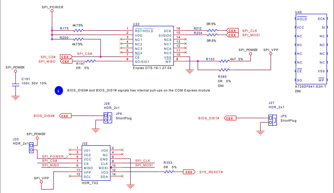
The BIOS device shown in Figure 46: SPI Reference Schematics is an Atmel AT25DF641-S3H flash memory device in a 16-SOIC package. The reference design above shows a socketed implementation, using a 16-pin SOIC socket, Enplas OTS-16-1.27-04. This surface-mount socket is footprint compatible with the SOIC-16 device, allowing for the PCB to be laid out such that the socket or the BIOS flash device itself is soldered to the Carrier Board. Of course a device with smaller package size (8-pin SOIC) can be used if a smaller footprint socket or device in use.
The flash device is connected via the SPI interface to the Module. SPI\_POWER, coming from the Module is used as power source for the device.
Flash device pin 7 is the chip enable signal and is connected to the chip select pin SPI\_CS# from the Module. Pin 8 is the data output signal of the flash chip and it is connected to the Module's SPI input SPI\_MISO. PIN 15 is the data input signal of the flash chip and it is connected to the SPI output SPI\_MOSI.
The optional connector J32 offers the possibility to program the flash device with an external programmer.
The flash device can be used with the Module when the jumper JP5 is set. JP6 will enable the LPC firmware hub, which is already mentioned in chapter 9.2 'LPC Firmware Hub' on page 207 below.
# 2.17.3. Routing Considerations
The SPI signals SPI\_MISO, SPI\_MOSI, SPI\_CS# and SPI\_CLK should be routed with a maximum length of 4.5” and should match to each other within 0.1”.
# 2.18. General Purpose I2C Bus Interface
The I2C (Inter-Integrated Circuit) bus is a two-wire serial bus originally defined by Philips. The bus is used for low-speed (up to 400kbps) communication between system ICs. The bus is often used to access small serial EEPROM memories and to set up IC registers. The COM Express Specification defines several I2C interfaces that are brought to the Module connector for use on the Carrier. Some of these interfaces are for very specific functions (VGA, LVDS, and DDIX), one interface is the SMBus used primarily for management and one other interface is a general purpose I2C interface. Since COM.0 Rev. 2.0 this interface should support multi-master operation. This capability will allow a Carrier to read an optional Module EEPROM before powering up the Module.
Revision 1.0 of the specification placed the I2C interface on the non-standby power domain. With this connection, the I2C interface can only be used when the Module is powered on. Since the I2C interface is used to connect to an optional Carrier EEPROM and since it is desirable to allow a Module based board controller access to the optional Carrier EEPROM before the Module is powered on, revision 2.0 of this specification changes the power domain of the I2C interface to standby-power allowing access during power down and suspend states. There is a possible leakage issue that can arise when using a R2.0 Module with a R1.0 Carrier that supports I2C devices. The R1.0 Carrier will power any I2C devices from the non-standby power rail. A R2.0 Module will pull-up the I2C clock and data lines to the standby-rail through a 2.2K resistor. The difference in the power domains on the Module and Carrier can provide a leakage path from the standby power rail to the non-standby power rail.
Vendor interoperability is given via EAPI – Embedded Application Programming Interface, which allows and easier interoperability of COM Express Modules.
# 2.18.1. Signal Definitions
The general purpose I2C Interface is powered from 3.3V suspend rail. The I2C\_DAT is an open collector line with a pull-up resistor located on the Module. The I2C\_CK has a pull-up resistor located on the Module. The Carrier should not contain pull-up resistors on the I2C\_DAT and I2C\_CK signals. Carrier based devices should be powered from 3.3V suspend voltage. The use of main power line for a Carrier I2C device will require a bus isolator to prevent leakage to other I2C devices on 3.3V power.
At this time, there is no allocation of I2C addresses between the Module and Carrier. Carrier designers will need to consult with Module providers for address ranges that can be used on the Carrier.
A reference to the I2C source specification can be found in Section 8 'Applicable Documents and Standards' on page 199.
The COM Express general purpose I2C pins are on the B row of the COM Express A-B connector as shown in Table 38 below.
Table 37: General Purpose I2C Interface Signal Descriptions
| Signal | Pin | Description | I/O | Pwr Rail | Comment |
| I2C_CK | B33 | General Purpose I2C Clock output | I/O ODCMOS | 3.3VSuspend | |
| I2C_DAT | B34 | General Purpose I2C data I/O line. | I/O ODCMOS | 3.3VSuspend | |
# 2.18.2. Reference Schematics
The COM Express specification recommends implementing a serial I2C EEPROM of at least 2kbit on the Carrier Board where all the necessary system configuration can be saved. For more information about the content of this system configuration EEPROM, refer to the COM Express
Specification. The circuitry in Figure 47 below shows how to connect an Atmel 'AT24C04' 4kbit EEPROM to the General Purpose I2C bus on the COM Express Carrier Board (http://www.atmel.com). According to the COM Express specification, the I2C address lines A2, A1 and A0 of the system configuration EEPROM must be pulled high. Depending on the EEPROM size this leads to the I2C addresses 1010 111x (2kbit), 1010 110x (4kbit), or 1010 100x (8kbit).
Figure 47: System Configuration EEPROM Circuitry
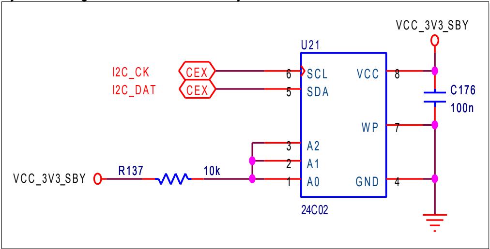
The EEPROM stores configuration information for the system of the Carrier Board. The data structure used is defined in the PICMG EEEP Specification. The Specification recommends but does not require the use of this system configuration EEPROM. The Module BIOS may check the Carrier Board configuration EEPROM but is not required to do so by the Specification.
The Atmel AT24C02 with 2Kb organized as 256 x 8 is a suitable device in an 8-pin SOIC package. For applications that require additional ROM or memory capacity such as 8Kb (1K x 8) or 16Kb (2K x 8), an Atmel AT24C08A may be used.
The COM Express Specification requires a minimum capacity of 2Kb. The Atmel AT24C02 meets this minimum capacity.
Address inputs A0, A1, A2 are pulled high. This creates the I2C address 1010 111x, which is required by the COM Express Specification. EEPROM devices internally set I2C address lines A6, A5, A4, A3 to binary value 1010.
WP (write protect) is pulled low for normal read/write.
# 2.18.3. Connectivity Considerations
The maximum amount of capacitance allowed on the Carrier General Purpose I2C bus lines (I2C\_DAT, I2C\_CK) is specified by your Module vendor. The Carrier designer is responsible for ensuring that the maximum amount of capacitance is not exceeded and the rise/fall times of the signals meet the I2C bus specification. As a general guideline, an IC input has 8pF of capacitance, and a PCB trace has 3.8pF per inch of trace length.
# 2.19. System Management Bus (SMBus)
The SMBus is primarily used as an interface to manage peripherals such as serial presence detect (SPD) on RAM, thermal sensors, PCI/PCIe devices, smart battery, etc. The devices that can connect to the SMBus can be located on the Module and Carrier. Designers need to take note of several implementation issues to ensure reliable SMBus interface operation. The SMBus is similar to I2C. I2C devices have the potential to lock up the data line while sending information and require a power cycle to clear the fault condition. SMBus devices contain a timeout to monitor for and correct this condition. Designers are urged to use SMBus devices when possible over standard I2C devices. COM Express Modules are required to power SMBus devices from Early Power in order to have control during system states S0-S5. The devices on the Carrier Board using the SMBus are normally powered by the 3.3V main power. To avoid current leakage between the main power of the Carrier Board and the Suspend power of the Module, the SMBus on the Carrier Board must be separated by a bus switch from the SMBus of the Module. Figure 48 below shows an appropriate bus switch circuit for separating the SMBus of the Carrier Board from the SMBus of the Module. However, if the Carrier Board also uses Suspend powered SMBus devices that are designed to operate during system states S3-S5, then these devices must be connected to the Suspend powered side of the SMBus, i. e. between the COM Express Module and the bus switch. Since the SMBus is used by the Module and Carrier, care must be taken to ensure that Carrier based devices do not overlap the address space of Module based devices. Typical Module located SMBus devices and their addresses include memory SPD (serial presence detect 1010 000x, 1010 001x), programmable clock synthesizes (1101 001x), clock buffers (1101 110x), thermal sensors (1001 000x), and management controllers (vendor defined address). Contact your Module vendor for information on the SMBus addresses used.
Figure 48: System Management Bus Separation
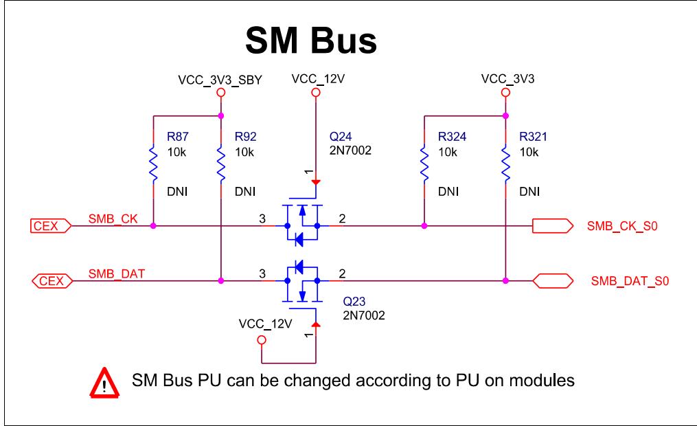
# 2.19.1. Signal Definitions
Table 38: System Management Bus Signals
| Signal | Pin | Description | I/O | Pwr Rail | Comment |
| SMB_CK | B13 | System Management Bus bidirectional clock line | I/O OD CMOS | 3.3V Suspend rail | |
| SMB_DAT | B14 | System Management bidirectional data line. | I/O OD CMOS | 3.3V Suspend rail | |
| SMB_ALERT# | B15 | System Management Bus Alert | I CMOS | 3.3V Suspend Rail | |
# 2.19.2. Routing Considerations
The SMBus should be connected to all or none of the PCIe/PCI devices and slots. A general recommendation is to not connect these devices to the SMBus.
The maximum load of SMBus lines is limited to 3 external devices. Please contact your Module vendor if more devices are required.
Do not connect Non-Suspend powered devices to the SMBus unless a bus switch is used to prevent back feeding of voltage from the Suspend rail to other supplies.
Contact your Module vendor for a list of SMBus addresses used on the Module. Do not use the same address for Carrier located devices.
# 2.20. General Purpose Serial Interface
Since Revision 2.0 of the COM Express specification two optional serial ports are available on Type 10 and Type 6 COM Express Modules uses pins on the A-B connector that have been reclaimed from the A-B VCC\_12V pool. As such, it is possible that if a Type 6 or 10 Module is deployed in an R1.0 Carrier Board for Module Types 1,2,3,4,5 then the Module TTL level serial pins may be exposed to the 12V supply, and Module designers must plan for this. Similarly, an R1.0 Module deployed on an R2.0 Carrier may bridge 12V to the serial pins and Carrier designers must plan for this. These pins are designated SER0\_TX, SER0\_RX, SER1\_TX and SER1\_RX. Data out of the Module is on the \_TX pins. Please refer to section 2.22.10 'Protecting COM.0 Pins Reclaimed From the VCC\_12V Pool' on page 144 below. Hardware handshaking and hardware flow control are not supported.
# 2.20.1. Signal Definitions
Table 39: General Purpose Serial Interface Signal Definition
| Signal | Pin | Description | I/O |
| SER0_TX | A98 | Transmit Line for Serial Port 0 | O CMOS (protected) |
| SER0_RX | A99 | Receive Line for Serial Port 0 | I CMOS (protected) |
| SER1_TX | A101 | Transmit Line for Serial Port 1 (can be shared with CAN function) | O CMOS (protected) |
| SER1_RX | A102 | Receive Line for Serial Port 1 (can be shared with CAN function) | I CMOS (protected) |
In Revision 2.0 of COM Express Specification these signals have been reclaimed from the VCC\_12V pool. Therefore protection on the Module and on the Carrier Board is necessary to avoid damage to those when accidentally exposed to 12V.
# 2.20.2. Reference Schematics
# 2.20.2.1. General Purpose Serial Port Example
Figure 49: General Purpose Serial Port Example
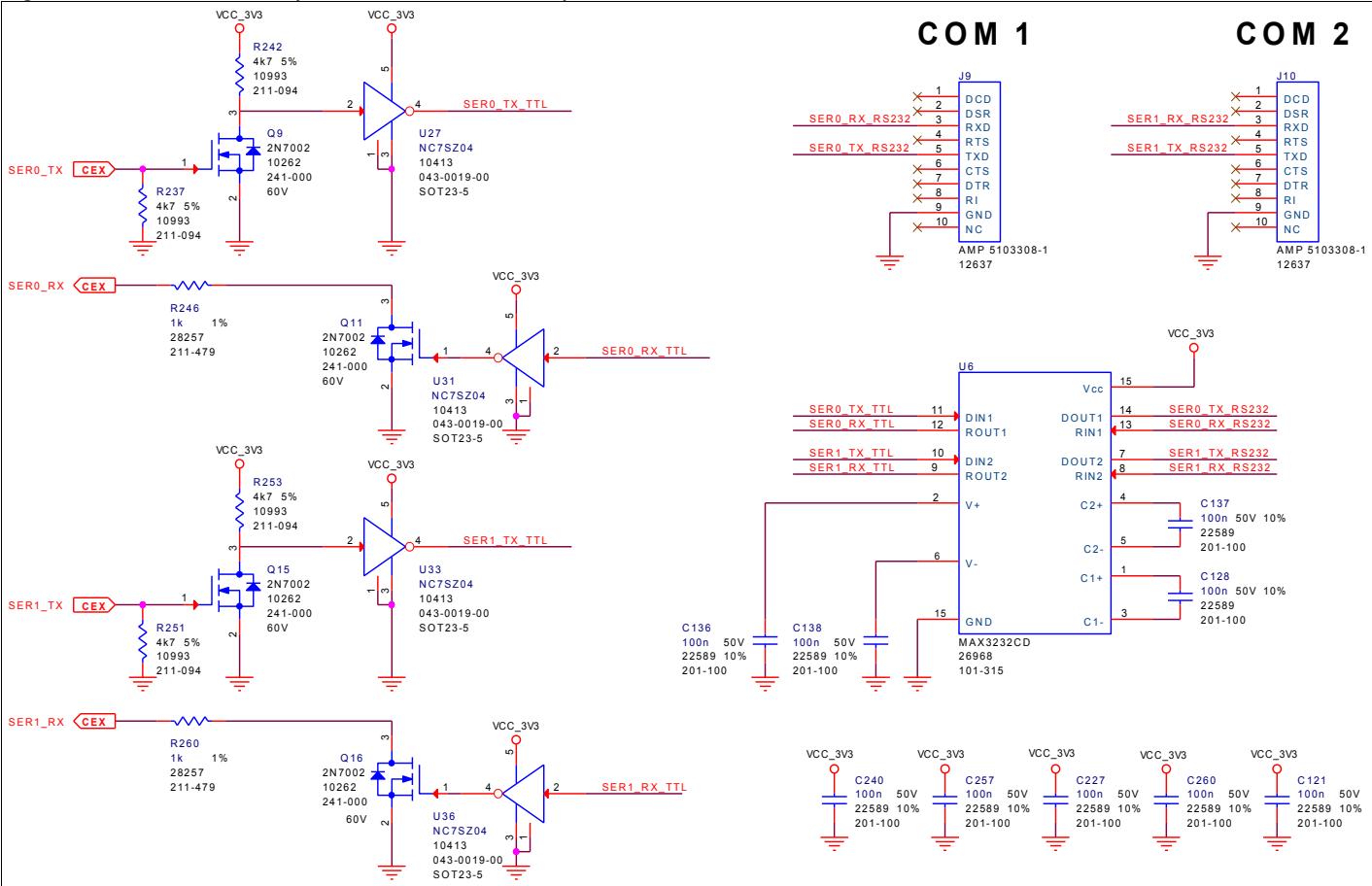
Figure 49: General Purpose Serial Port Example shows the schematic of two general purpose serial ports with RS232 level shifter (U6). The transistor / inverter combination at the serial TX and RX lines coming from the Module is necessary to handle the protection against VCC\_12V connection according to chapter 5.10 of COM.0 Rev. 2.1. The MAX3232CD is a dual port RS232 transceiver and handles the level shifting of the TTL signals to the regarding voltage level.
Conformance to the protection scheme defined in COM.0 Rev 2 for pins recovered from the 12V pool results in a transfer rate limit of about 10 kbaud. If your situation requires higher speeds, contact your Module vendor for possible work-arounds. The work-arounds likely involve sacrificing the 12V protection as a tradeoff for higher speeds.
# 2.20.3. Routing Considerations
No further routing considerations need to be taken.
# 2.21. CAN Interface
CAN bus is a vehicle bus standard designed to allow controllers and devices to communicate with each other without a host computer. CAN bus is a message-based protocol, designed specifically for automotive applications but now also used in other areas such as industrial automation and medical equipment.
Development of CAN bus started originally in 1983. The protocol was officially released in 1986 at the Society of Automotive Engineers (SAE) congress in Detroit, Michigan. The first CAN controller chips, produced by Intel and Philips, came on the market in 1987. In 1991 the CAN 2.0 specification was published.
Since 2008 CAN bus has been mandatory in any US vehicle in the OBD-II car diagnostic port. It is also used extensively in industrial automation.
# 2.21.1. Signal Definitions
Table 40: CAN Interface Signal Definition
| Signal | Pin | Description | I/O |
| CAN_TX | A101 | Transmit Line for CAN (can be shared with SER1 function) | O CMOS (protected) |
| CAN_RX | A102 | Receive Line for CAN (can be shared with SER1 function) | I CMOS (protected) |
This signals have been introduced in COM.0 Specification Revision 2.1 optionally for Type 10 and Type 6 Modules. They have been reclaimed from the VCC\_12V pool. Therefore protection on the Module and on the Carrier Board is necessary that accidental exposure to 12V will not lead to either damaged Modules or Carrier Boards. Please refer to section 2.22.10 'Protecting COM.0 Pins Reclaimed From the VCC\_12V Pool' on page 144 below.
The protection, especially the series diode on the Module reduce the maximum speed on the CAN interface to about 10 Kbaud.
The CAN port consists of an asynchronous CAN TX line and an RX line from and to the COM Express Module CAN protocol controller. A Carrier based CAN transceiver is required to realize a CAN implementation. CAN PHYs are available from Texas Instruments, On Semiconductor, NXP, Freescale, Microchip and numerous other vendors.
CAN bus on COM Express is an optional interface, which means that the system designer must verify, if the selected Module supports it.
# 2.21.2. Reference Schematics
# 2.21.2.1. CAN Bus Example
Figure 50: CAN Bus Example
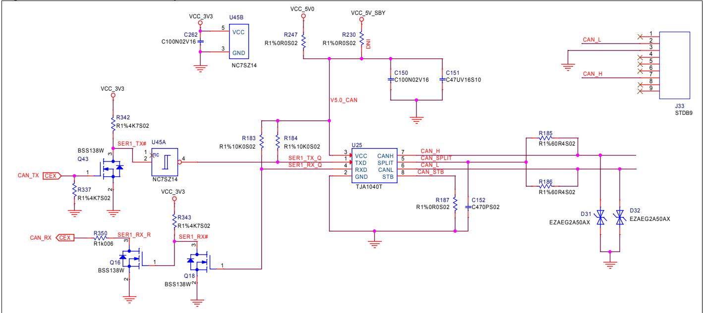
Figure 50: CAN Bus Example shows the schematics of a CAN Bus implementation with the CAN Transceiver TJA10407 (U25). The transistor / inverter combination at the CAN\_TX and CAN\_RX line coming from the Module is necessary to handle the protection against VCC\_12V connection according to chapter 5.10 of COM.0 Rev. 2.1. The Diodes D31 and D32 accomplish ESD protection.
J33 is a DSUB-9 connector in standardized CAN pin-out. Please refer to Table 41: Pin-out Table DSUB-9 CAN Connector below.
If an ODB-II adapter is used pin 9 carries the car battery voltage. The automotive power rail is a difficult rail to work with. It is nominally a 12V rail but may dip to 6V when the engine is cranking and may be up to 16V when the engine is running and there may be transients in excess of +/- 100V.
Table 41: Pin-out Table DSUB-9 CAN Connector
| J33 (9 positions) | Pin description |
| 2 | CAN_L |
| 7 | CAN_H |
| 9 | VCC |
| 3 | GND |
The COM Express Specification conform 12V protection will decrease the maximum transfer rate to about 10kbaud. For higher speed please contact your Module vendor to find a solution.
# 2.21.3. Routing Considerations
It should be routed as a differential pair signal with 120 Ohm differential impedance. The end points of CAN bus should be terminated with 120 Ohms or with 60 Ohms from the CAN\_H line and 60 Ohms from the CAN\_L line to the CAN Bus reference voltage. Check your CAN transceiver application notes for further details on termination.
# 2.22. Miscellaneous Signals
Table 42: Miscellaneous Signals
| Signal | Pin | Description | I/O | Comment |
| TYPE0# | C54 | The Type pins indicate the COM Express pin-out type of the Module. To indicate the Module's pin-out type, the pins are either not connected or strapped to ground on the Module. The Carrier Board has to implement additional logic, which prevents the system to switch power on, if a Module with an incompatible pin-out type is detected. | O 5V PDS | Only Available on T2-T6 |
| TYPE1# | C57 |
| TYPE2# | D57 |
| TYPE10# | A97 | Indicates to the Carrier Board that a Type 10 Module is installed. Indicates to the Carrier Board, that a Rev 1.0/2.0 Module is installed.TYPE10#NC Pin-out R2.0PD Pin-out Type 10 pull down to ground with 47k12V Pin-out R1.0 | | |
| SPKR | B32 | Output used to control an external FET or a logic gate to drive an external PC speaker. | O 3.3V CMOS | |
| BIOS_DISABLE0# | A34 | Selection straps to determine the BIOS boot device. The Carrier should only float these or pull them low, | I 3.3V CMOS | See Section 2.17 'SPI - Serial Peripheral Interface Bus' on page 118 above |
| BIOS_DISABLE1# | B88 | Selection straps to determine the BIOS boot device. The Carrier should only float these or pull them low, | I 3.3V CMOS | See Section 2.17 'SPI - Serial Peripheral Interface Bus' on page 118 above |
| WDT | B27 | Output indicating that a watchdog time-out event has occurred. | O 3.3V CMOS | |
| KBD_RST# | A86 | Input signal of the Module used by an external keyboard controller to force a system reset. | I 3.3V CMOS | Only Available on T1-T5 |
| KBD_A20GATE | A87 | Input signal of the Module used by an external keyboard controller to control the CPU A20 gate line. The A20 gate restricts the memory access to the bottom megabyte of the system. Pulled high on the Module. | I 3.3V CMOS | Only Available on T1-T5 |
| LID# | A103 | LID switch.Low active signal used by the ACPI operating system for a LID switch. | I 3.3V CMOS OD | Only Available on T6 and T10 |
| SLEEP# | B103 | Sleep button.Low active signal used by the ACPI operating system to bring the system to sleep state or to wake it up again. | I 3.3V CMOS OD | Only Available on T6 and T10 |
| $FAN\_PWMOUT^1$ | B101 | Fan speed control. Uses the Pulse Width Modulation (PWM) technique to control the fan's RPM. | O 3.3V CMOS OD | Only Available on T6 and T10 |
| $FAN\_TACHIN^1$ | B102 | Fan tachometer input for a fan with a two pulse output. | I 3.3V CMOS OD | Only Available on T6 and T10 |
| TPM_PP $^1$ | A96 | Trusted Platform Module (TPM) Physical Presence pin. Active high. TPM chip has an internal pull down. This signal is used to indicate Physical Presence to the TPM. | I 3.3V CMOS | Only Available on T6 and T10 |
| GPO0 | A93 | General Purpose Outputs for system specific usage. | O 3.3V CMOS | Refer to the Module's users guide for information about the functionality of these signals. |
| GPO1 | B54 |
| GPO2 | B57 |
| GPO3 | B63 |
| GPI0 | A54 | General Purpose Input for system specific usage. The signals are pulled up by the Module. | I 3.3V CMOS | Refer to the Module's users guide for information about the functionality of these signals. |
| GPI1 | A63 |
| GPI2 | A67 |
| GPI3 | A85 |
# 2.22.1. Module Type Detection
The COM Express Specification includes three signals to determine the pin-out type of the Module connected to the Carrier Board. If an incompatible Module pin-out type is detected, external logic should prevent the Carrier Board from powering up the whole system by controlling the 12V supply voltage. The pins 'TYPE0#', 'TYPE1#' and 'TYPE2#' are either left open (NC) or strapped to ground (GND) by the Module to encode the pin-out type according to the following table. The Module Type 1 has no encoding. For more information about this subject, refer to the COM Express Specification.
Table 43: Module Type Detection
| Module Type | Pin TYPE0# | Pin TYPE1# | Pin TYPE2# | Pin TYPE10# | |
| Module Type 1 | X (don't care) | X (don't care) | X (don't care) | 12V or NC | |
| Module Type 2 | NC | NC | NC | 12V or NC | |
| Module Type 3 | NC | NC | GND | 12V or NC | No IDE interface |
| Module Type 4 | NC | GND | NC | 12V or NC | No PCI interface |
| Module Type 5 | NC | GND | GND | 12V or NC | No IDE, no PCI interface |
| Module Type 6 | GND | NC | NC | 12V or NC | No IDE, no PCI interface |
| Module Type 10 | X (don't care) | X (don't care) | X (don't care) | PD with 47k | |
Pin TYPE10# is reclaimed from the VCC\_12V pool. In R1.0 Modules this pin will connect to other VCC\_12V pins. In R2.0 this pin is defined as a no connect for types 1-6. A Carrier can detect a R1.0 Module by the presence of 12V on this pin. R2.0 Module types 1-6 will no connect this pin. Type 10 Modules shall pull this pin to ground through a 47K resistor.
Figure 51 below illustrates a detection circuitry for Type 2 Modules. If any Module type other than Type 2 is connected, the 'PS\_ON#' signal, which controls the ATX power supply, is not driven low by the Module, and hence the main power rails of the ATX supply do not come up. The Type Detection pins of the Module must be pulled up on the Carrier Board to the 5V Suspend voltage rail.
Figure 51: Module Type 2 Detection Circuitry
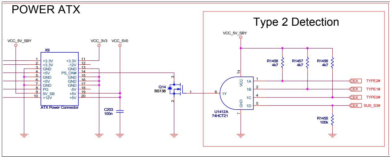
# 2.22.2. 5 Speaker Output+12V 3+12V4
The PC-AT architecture provides a speaker signal that creates beeps and chirps. The signal is a digital-logic signal that is created from system timers within the core chipset. The speaker provides feedback to the user that an error has occurred. The system BIOS usually drives the speaker line with a set of beep codes to indicate hardware problems such as a memory test POWER AT failure, a missing video device, or a missing keyboard. Application software often uses the PC-AT speaker to flag an error such as an invalid key press.
This speaker signal should not be confused with the analog-audio signals produced by the audioT CODEC. In many systems, the PC-AT speaker signal is fed into one of the audio CODEC inputs,TT Power Connector allowing it to be mixed with other audio signals and heard on the audio transducer (speakers andT headphones) that the CODEC drives.
The COM Express Module provides a speaker output signal called 'SPKR', which is intended to drive an external FET or a logic gate to connect a PC speaker.
The 'SPKR' signal is often used as a configuration strap for the Modules chipset. It should not be connected to a pull-up or pull-down resistor, which could overwrite the internal chipset configuration and result in a malfunction of the Module.
The PC-AT audio transducer that is used for error messages is usually a small, low-cost loudspeaker or piezoelectric-electric buzzer. A buffering between the Module SPKR pin and the audio transducer is required. An example circuit is shown in Figure 52 below. The net SPKR is sourced from Module pin B32. If the transducer is a low impedance device, such as an 8 Ω speaker, then a larger resistor value and package size for R173/R175 is in order.
Figure 52: Speaker Output Circuitry
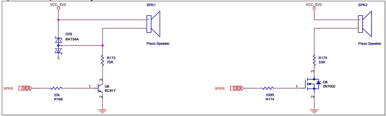
# 2.22.3. RTC Battery Implementation
The Real Time Clock (RTC) is responsible for maintaining the time and date even when the COM Express Module is not connected to a main power supply. Usually a +3V lithium battery cell is used to supply the internal RTC of the Module. The COM Express Specification defines an extra power pin 'VCC\_RTC', which connects the RTC of the Module to the external battery. The specified input voltage range of the battery is defined between +2.0V and +3.0V. The signal 'VCC\_RTC' can be found on the Module's connector row A pin A47.
To implement the RTC Battery according to the Underwriters Laboratories Inc® (UL) guidelines (UL 1642), battery cells must be protected against a reverse current going to the cell. UL 1642 requires two blocking components (such as a pair of diodes) or a resistor and a diode. The resistor has to be large enough to prevent a current of more than one third of the battery's maximum allowed reverse charging current. An alternative to a pair of diodes are specialty ICs from companies such as Maxim or Dallas Semiconductor that have a UL1642 approval and perform the required blocking function.
The resistor and diode option is shown in Figure 53 below.
A possible drawback of this circuitry is that the battery voltage monitoring result displayed by the COM Express Module will be inaccurate due to current leakage on the Module side. When the system is running, this current leakage loads the capacitor of the battery circuitry. This leads to a higher voltage on the signal pin 'VCC\_RTC' and therefore produces inaccurate monitoring results.
Figure 53: RTC Battery Circuitry with Serial Schottky Diode
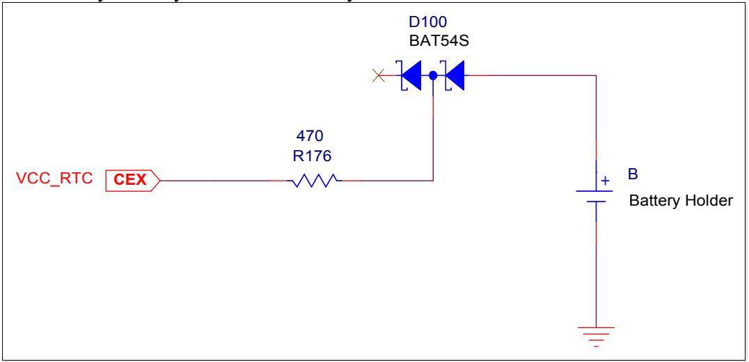
# 2.22.3.1. RTC Battery Lifetime
The RTC battery lifetime determines the time interval between system battery replacement cycles. Current leakage from the RTC battery circuitry on the Carrier Board is a serious issue and must be considered during the system design phase. The current leakage will influence the RTC battery lifetime and must be factored in when a specific life expectancy of the system battery is being defined.
In order to accurately measure the value of the RTC current, it should be measured when the complete system is disconnected from primary power.
For information about the power consumption of the RTC circuit, refer to the Module's user's guide.
# 2.22.4. Power Management Signals
COM Express specifies a set of signals to control the system power states such as the power-on and reset conditions. This enables the system designer to implement a fully ACPI compliant system supporting system states from S0 to S5. The minimum hardware requirements for an ACPI compliant system are an ATX conforming power supply and a power button.
The following table provides a short description of the ACPI defined system states S0 to S5 including the corresponding power rail state. For more information about ACPI and the several system power states, refer to the 'Advanced Configuration and Power Interface Specification Revision'.
Table 44: System States S0-S5 Definitions
| System State | Description | Power Rail State |
| S0Full On | All components are powered and the system is fully functional. | Full power on all power rails. |
| S1Power-on Standby (POS) | In sleeping state, no system context is lost, hardware maintains all system context. During S1 operation some system components are set into low power state. | Full power on all power rails. |
| S2 | Not supported. | |
| S3Suspend to RAM (STR) | The current system state and context is stored in main memory and all unnecessary system logic is turned off. | Only main memory and logic required to wake-up the system remain powered by the Suspend voltages. All other power rails are switched off. |
| S4Suspend to Disk (STD)Hibernate | The current system state and context is stored on disk and all unnecessary system logic is turned off. S4 is similar to S5 and just supported by OS. | Similar to S5; All other power rails are switched off. |
| S5Soft Off | In S5 state the system is switched off. Restart is only possible with the power button or by a system wake-up event such as 'Wake On LAN' or RTC alarm. | Suspend power rails are powered. All other power rails are switched off. |
Table 45: Power Management Signal Descriptions
| Signal | Pin | Description | I/O | Comment |
| PWRBTN# | B12 | Power button low active signal used to wake up the system from S5 state (soft off). This signal is triggered on the falling edge. | I 3.3V Suspend CMOS | Drive with >=10mA |
| SYS_RESET# | B49 | Reset button input. Active low request for Module to reset and reboot. May be falling edge sensitive. For situations when SYS_RESET# is not able to reestablish control of the system, PWR_OK or a power cycle may be used. | I 3.3V Suspend CMOS | Drive with >=10mA |
| CB_RESET# | B50 | Reset output signal from Module to Carrier Board. This signal may be driven low by the Module to reset external components located on the Carrier Board. | O 3.3V Suspend CMOS | |
| PWR_OK | B24 | Power OK status signal generated by the ATX power supply to notify the Module that the DC operating voltages are within the ranges required for proper operation. | I 3.3V CMOS | |
| SUS_STAT# | B18 | Suspend status signal to indicate that the system will be entering a low power state soon. It can be used by other peripherals on the Carrier Board as an indication that they should go into power-down mode. | O 3.3V Suspend CMOS | |
| SUS_S3# | A15 | S3 Sleep control signal indicating that the system resides in S3 state (Suspend to RAM). | O 3.3V Suspend CMOS | This signal can be used to control the ATX power supply via the 'PS_ON#' signal. |
| SUS_S4# | A18 | S4 Sleep control signal indicating that the system resides in S4 state (Suspend to Disk). | O 3.3V Suspend CMOS | |
| SUS_S5# | A24 | S5 Sleep Control signal indicating that the system resides in S5 State (Soft Off). | O 3.3VSuspendCMOS | |
| WAKE0# | B66 | PCI Express wake-up event signal. | I 3.3V SuspendCMOS | |
| WAKE1# | B67 | General purpose wake-up signal. | I 3.3V SuspendCMOS | |
| BATLOW# | A27 | Battery low input. This signal may be driven low by external circuitry to signal that the system battery is low. It also can be used to signal some other external power management event. | I 3.3V SuspendCMOS | |
# 2.22.5. Watchdog Timer
Figure 54: Watchdog Timer Event Latch Schematic
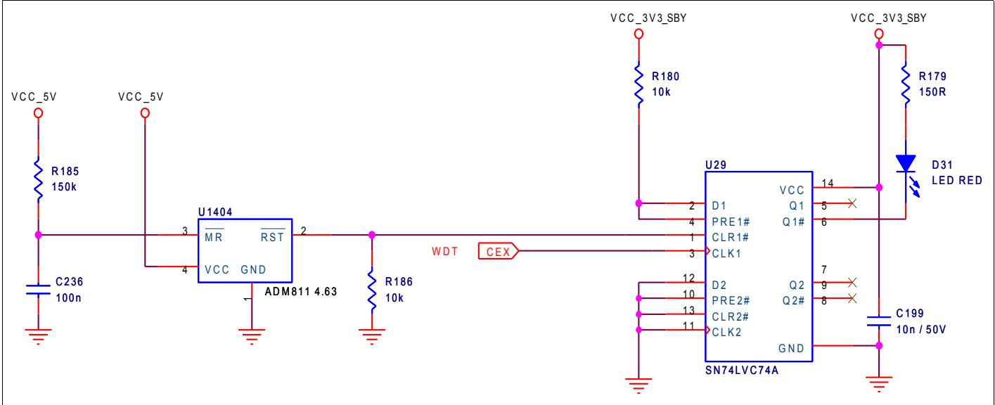
The Watchdog Timer (WDT) event signal is provided by the COM Express Module. The WDT output is active-high. It is sourced from Module pin B27.
The WDT event can cause the system to reset by making appropriate Carrier Board connections. It also may be possible to configure the Module to reset on a WDT event; check the manufacturer's Module Users Guide.
If the WDT output is used to cause a system reset, the WDT output will be cleared by the system reset event.
The WDT can be latched to drive a LED for a visual indication of an event, as shown in this example. The latch is only cleared by a complete power cycle.
# 2.22.6. General Purpose Input/Output (GPIO)
Table 46: GPIO Signal Definition
| Signal | Pin | Description | I/O | Comment |
| GPI0 | A54 | General purpose input pins. Pulled high internally on the Module. | I 3.3V CMOS | |
| GPI1 | A63 | General purpose input pins. Pulled high internally on the Module. | I 3.3V CMOS | |
| GPI2 | A67 | General purpose input pins. Pulled high internally on the Module. | I 3.3V CMOS | |
| GPI3 | A85 | General purpose input pins. Pulled high internally on the Module. | I 3.3V CMOS | |
| GPO0 | A93 | General purpose output pins. Upon a hardware reset, these outputs should be low. | O 3.3V CMOS | |
| GPO1 | B54 | General purpose output pins. Upon a hardware reset, these outputs should be low. | O 3.3V CMOS | |
| GPO2 | B57 | General purpose output pins. Upon a hardware reset, these outputs should be low. | O 3.3V CMOS | |
| GPO3 | B63 | General purpose output pins. Upon a hardware reset, these outputs should be low. | O 3.3V CMOS | |
Figure 55: General Purpose I/O Loop-back Schematic
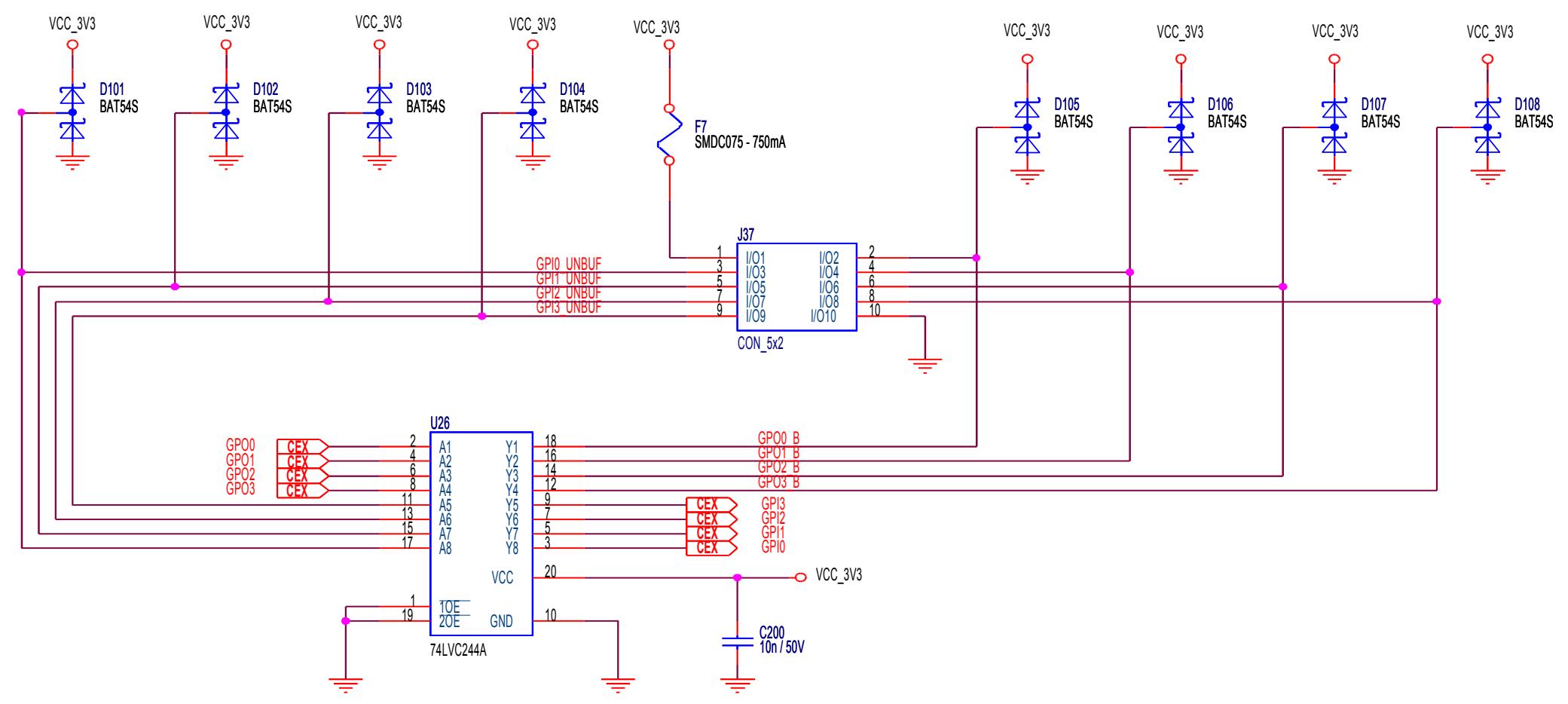
There are 4 GPI (General Purpose Inputs) and 4 GPO (General Purpose Outputs) pins in Figure 55 above.
The signals drive switch inputs such as Lamps, Relays, and Sensors.
GPI signals from a header are shown with protection diodes. The signals are connected for input to the COM Express Module.
GPO signals from the COM Express Module are shown buffered. The signals are connected to the header with protection diodes.
# 2.22.7. SDIO Interface Multiplexed with GPIOs
SD Card support was added in COM.0 Rev. 2.0 as an alternative use for the GPIO pins. The schematic below shows a multiplexer allowing the carrier to use the COM Express pins either as GPIO or as an SD Card interface. In a dedicated application the multiplexer is not necessary – if you just want an SD Card interface and no GPIO you can route the pins directly from the COM Express connectors to the SD Card. It is important that the SD Cards are ESD protected.
The following notes apply to Figure 56: SDIO Interface Multiplexed with GPIOs below.
U19 is the switch device to determine the usage of the GPI0 to GPI3 and GPO0 to GPO3 coming from the COM Express Module. When Jumper J39 is set to GND, SDIO is supported. When J39 is open, GPIO is supported. Please verify that the Module used supports the intended interface. To simplify the circuit, instead of installing U19, resistors R220 to R225, R227 and R249 can be installed when only SDIO is necessary without the usage of GPIOs.
Maximum length for SDIO should be restricted to 3 inches to the SDIO connector. Additional EMI or ESD measures might be applicable.
Figure 56: SDIO Interface Multiplexed with GPIOs
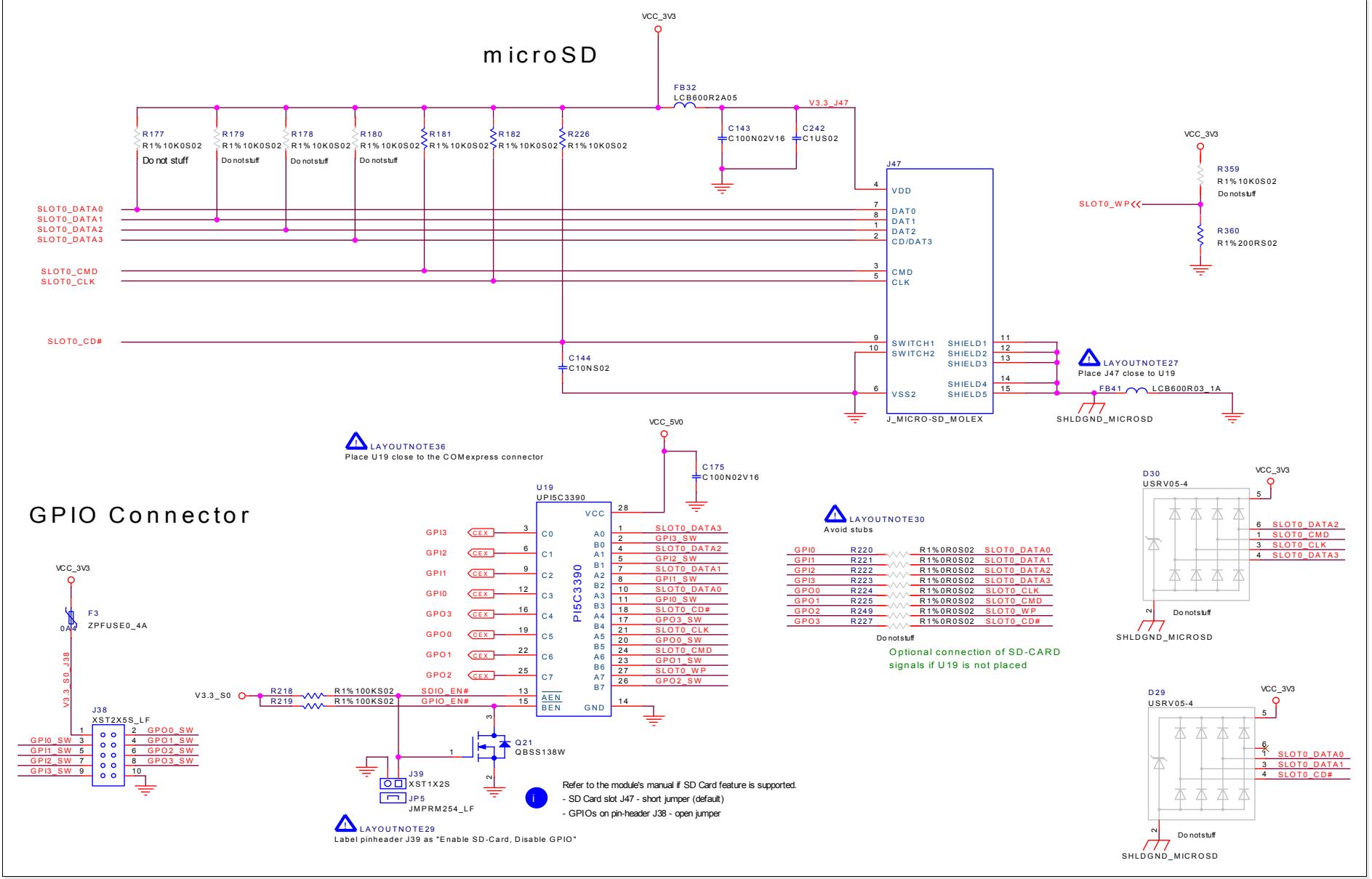
# 2.22.8. Fan Connector
Figure 57: Fan Connector Reference Schematic
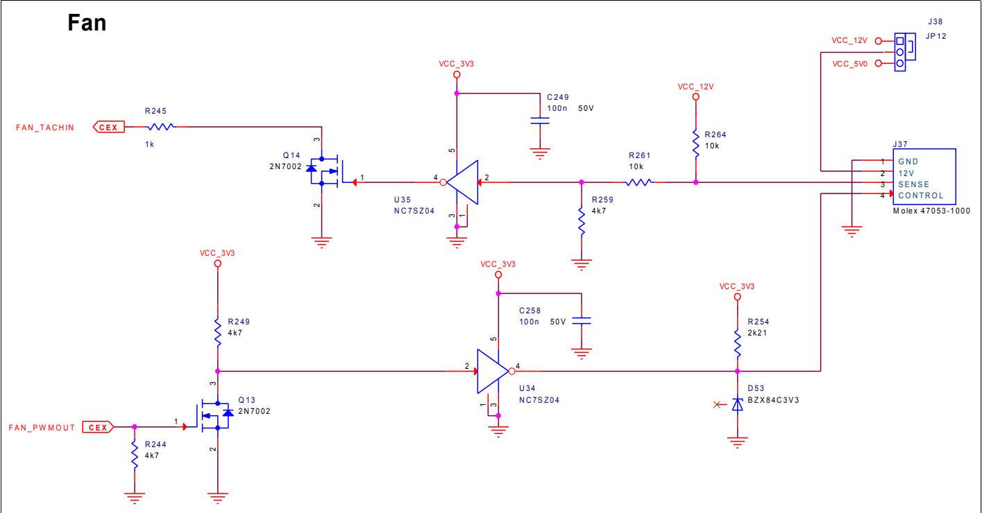
FAN\_TACHIN and FAN\_PWMOUT in Figure 57: Fan Connector Reference Schematic above are COM.0 pins reclaimed from the VCC\_12V pool. Q13 / Q14 and U34 / U35 are the necessary circuitry on the Carrier Board to handle the 12V protection according to chapter 2.22.10 'Protecting COM.0 Pins Reclaimed From the VCC\_12V Pool' on page 144 below. This reference schematic shows a 4-wire fan implementation, which should be preferred over a 3-wire fan. 4- wire fan implementations allow better sensing and control of the fan.
# 2.22.9. Thermal Interface
COM Express provides the 'THRM#' and 'THRMTRIP#' signals, which are used for system thermal management. In most current system platforms, thermal management is closely associated with system power management. For more detailed information about the thermal management capabilities of the COM Express Module, refer to the manufacturer's Module's user's guide.
Table 47: Thermal Management Signal Descriptions
| Signal | Pin | Description | I/O | Comment |
| THRM# | B35 | Thermal Alarm active low signal generated by the external hardware to indicate an over temperature situation. This signal can be used to initiate thermal throttling. | I 3.3V CMOS | |
| THRMTRIP# | A35 | Thermal Trip indicates an overheating condition of the processor. If 'THRMTRIP#' goes active the system immediately transitions to the S5 State (Soft Off). | O 3.3V CMOS | |
# 2.22.10. Protecting COM.0 Pins Reclaimed From the VCC\_12V Pool
The COM.0 Rev. 2 Type 6 and Type 10 pin-out types introduce eight signals that are mapped to pins that are re-claimed from pins that are VCC\_12V supply pins on Type 1,2,3,4 and 5 Modules. These signals include
SER0\_TX, SER1\_TX TTL level outputs from the Module
SER0\_RX, SER1\_RX TTL level inputs to the Module
LID#, SLEEP# 3.3V logic level inputs to the Module, in the suspend domain
FAN\_TACHIN 3.3V logic level input to the Module
FAN\_PWMOUT 3.3V logic level output from the Module
A new Type strap pin is also introduced in COM.0 Rev 2, for all Module Types. It also falls on a pin that was used exclusively for VCC\_12V in COM.0 Rev. 1:
TYPE10# VCC\_12V on COM.0 Rev. 1 Module Types 1,2,3,4,5 No connect on COM.0 Rev. 2 Module Types 1,2,3,4,5,6 47K Module pull-down to GND on Module Type 10
All nine of the signals referenced above on COM.0 Rev. 2 compliant Module and Carrier designs shall be able to withstand continuous direct connections to low impedance 12V sources (i.e. a short to a 12V power supply).
One line of defense against such unintended connections is for Carrier designs to decode the Module TYPE pins (3 pins on the C-D connector, and the new TYPE10# pin on the A-B connector) and to not power the system up if an improper Module Type is detected. Examples of this may be found in the PICMG Carrier Design Guide. However, there are some situations in which this can not be relied upon. One such situation is if a user plugs a Type 10 Module into a Rev. 1 Type 1 Carrier. Since the TYPE10# strap was not anticipated in the Rev. 1 Carrier, the Carrier will apply power to the Type 10 Module. Thus it is very important that Type 10 and 6 Modules be able to withstand 12V exposure to the pins reclaimed from the VCC\_12V pool.
# 2.22.10.1. Logic Level Signals on Pins Reclaimed from VCC\_12V
Module logic level inputs and outputs that are implemented on pins reclaimed from the VCC\_12V pool shall implement the series Schottky diode protection shown in the right side of the figure below. The Schottky diode should be a BAT54 device. For inputs in this group, a 47K pull-up to the local 3.3V S0 or S5 rail (as appropriate) shall be used.
Carrier Board logic level inputs and outputs that are implemented on pins reclaimed from the VCC\_12V pool shall be protected against protracted accidental exposure to 12V. The protection scheme shown in the left side of the Figure 5-13 below may be used. Any scheme that is used shall be able to pull the reclaimed Module input low enough such that Module CMOS input logic sees a maximum voltage of 0.5V for a logic low, as indicated in the figure.
Figure 58: Protecting Logic Level Signals on Pins Reclaimed from VCC\_12V
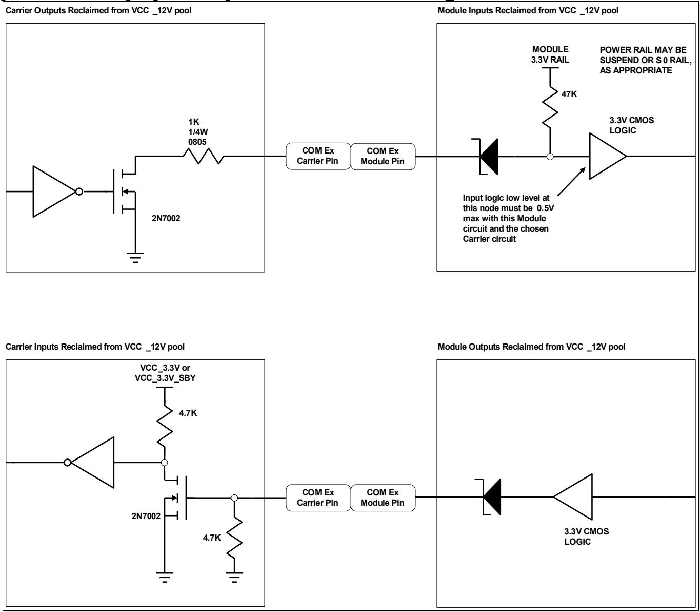
# 2.22.10.2. TYPE10# Strap - Reclaimed from VCC\_12V
No additional protection is needed for the TYPE10# strap on the Module side:
On Type 10 Modules, this pin is tied through a 47K resistor to GND. Exposure of this Module pin to 12V is harmless.
On Rev. 1 Type 1,2,3,4,5 Modules, this pin is tied to VCC\_12V already.
On Rev. 2 Type 1,2,3,4,5 Modules, this pin is a no connect.
On Type 6 Modules, this pin is a no connect.
On the Carrier side, protection against accidental 12V exposure is required. Carrier Board designs shall be tolerant of protracted VCC\_12V exposure on the TYPE10# pin. A Rev. 1 Type 1 Module, for example, would expose the TYPE10# pin on a Rev. 2 Type 1,2,3,4,5 Carrier to 12V (unless the Carrier design does not allow the system to power up for an incorrect Module type).
The TYPE10# Module pin is, in effect, a tri-level pin: it is tied, depending on Module Type and COM.0 Revision level, to either VCC\_12V, to nothing, or to GND through 47K. Carrier Board circuits can be created that distinguish between the 3 levels. If implemented, this would allow the Carrier Board to determine whether a Type 1,2,3,4,5 Module is a built to COM.0 Rev. 1 or Rev. 2. This may be illustrated in a future edition of the PICMG Carrier Design Guide.
# 2.23. PCI Bus
# 2.23.1. Signal Definitions
Type 2 and 3 COM Express Modules provide a 32-bit PCI bus that can operate up to 33 MHz. The corresponding signals can be found on the Module connector rows C and D.
Table 48: PCI Bus Signal Definition
| Signal | Pin# | Description | I/O | Comment |
| PCI_AD0 | C24 | PCI bus multiplexed address and data lines | I/O 3.3V | |
| PCI_AD1 | D22 | PCI bus multiplexed address and data lines | I/O 3.3V | |
| PCI_AD2 | C25 | PCI bus multiplexed address and data lines | I/O 3.3V | |
| PCI_AD3 | D23 | PCI bus multiplexed address and data lines | I/O 3.3V | |
| PCI_AD4 | C26 | PCI bus multiplexed address and data lines | I/O 3.3V | |
| PCI_AD5 | D24 | PCI bus multiplexed address and data lines | I/O 3.3V | |
| PCI_AD6 | C27 | PCI bus multiplexed address and data lines | I/O 3.3V | |
| PCI_AD7 | D25 | PCI bus multiplexed address and data lines | I/O 3.3V | |
| PCI_AD8 | C28 | PCI bus multiplexed address and data lines | I/O 3.3V | |
| PCI_AD9 | D27 | PCI bus multiplexed address and data lines | I/O 3.3V | |
| PCI_AD10 | C29 | PCI bus multiplexed address and data lines | I/O 3.3V | |
| PCI_AD11 | D28 | PCI bus multiplexed address and data lines | I/O 3.3V | |
| PCI_AD12 | C30 | PCI bus multiplexed address and data lines | I/O 3.3V | |
| PCI_AD13 | D29 | PCI bus multiplexed address and data lines | I/O 3.3V | |
| PCI_AD14 | C32 | PCI bus multiplexed address and data lines | I/O 3.3V | |
| PCI_AD15 | D30 | PCI bus multiplexed address and data lines | I/O 3.3V | |
| PCI_AD16 | D37 | PCI bus multiplexed address and data lines | I/O 3.3V | |
| PCI_AD17 | C39 | PCI bus multiplexed address and data lines | I/O 3.3V | |
| PCI_AD18 | D38 | PCI bus multiplexed address and data lines | I/O 3.3V | |
| PCI_AD19 | C40 | PCI bus multiplexed address and data lines | I/O 3.3V | |
| PCI_AD20 | D39 | PCI bus multiplexed address and data lines | I/O 3.3V | IDSEL for slot 0 |
| PCI_AD21 | C42 | PCI bus multiplexed address and data lines | I/O 3.3V | IDSEL for slot 1 |
| PCI_AD22 | D40 | PCI bus multiplexed address and data lines | I/O 3.3V | IDSEL for slot 2 |
| PCI_AD23 | C43 | PCI bus multiplexed address and data lines | I/O 3.3V | IDSEL for slot 3 |
| PCI_AD24 | D42 | PCI bus multiplexed address and data lines | I/O 3.3V | |
| PCI_AD25 | C45 | PCI bus multiplexed address and data lines | I/O 3.3V | |
| PCI_AD26 | D42 | PCI bus multiplexed address and data lines | I/O 3.3V | |
| PCI_AD27 | C46 | PCI bus multiplexed address and data lines | I/O 3.3V | |
| PCI_AD28 | D44 | PCI bus multiplexed address and data lines | I/O 3.3V | |
| PCI_AD29 | C47 | PCI bus multiplexed address and data lines | I/O 3.3V | |
| PCI_AD30 | D45 | PCI bus multiplexed address and data lines | I/O 3.3V | |
| PCI_AD31 | C48 | PCI bus multiplexed address and data lines | I/O 3.3V | |
| PCI_C/BE0# | D26 | PCI bus byte enable line 0, active low | I/O 3.3V | |
| PCI_C/BE1# | C33 | PCI bus byte enable line 0, active low | I/O 3.3V | |
| PCI_C/BE2# | C38 | PCI bus byte enable line 0, active low | I/O 3.3V | |
| PCI_C/BE3# | C44 | PCI bus byte enable line 0, active low | I/O 3.3V | |
| PCI_DEVSEL# | C36 | PCI bus Device Select, active low | I/O 3.3V | |
| PCI_Frame# | D36 | PCI bus Frame control line, active low | I/O 3.3V | |
| PCI_IRDY# | C37 | PCI bus Initiator Ready control line, active low | I/O 3.3V | |
| PCI_TRDY# | D35 | PCI bus Target Ready control line, active low | I/O 3.3V | |
| PCI_STOP# | D34 | PCI bus STOP control line, active low | I/O 3.3V | |
| PCI_PAR | D32 | PCI bus parity | I/O 3.3V | |
| PCI_PERR# | C34 | Parity Error: An external PCI device drivers PERR# by driving it low, when it receives data that has a parity error. | I/O 3.3V | |
| PCI_REQ0# | C22 | PCI bus master request input line, active low | I 3.3V | |
| PCI_REQ1# | C19 | PCI bus master request input line, active low | I 3.3V | |
| PCI_REQ2# | C17 | PCI bus master request input line, active low | I 3.3V | |
| PCI_REQ3# | D20 | PCI bus master request input line, active low | I 3.3V | |
| PCI_GNT0# | C20 | PCI bus master grant output line, active low | O 3.3V | |
| PCI_GNT1# | C18 | PCI bus master grant output line, active low | O 3.3V | |
| PCI_GNT2# | C16 | PCI bus master grant output line, active low | O 3.3V | |
| PCI_GNT3# | D19 | PCI bus master grant output line, active low | O 3.3V | |
| PCI_RESET# | C23 | PCI Reset output, active low | O 3.3V_SBY | Asserted during system reset |
| PCI_LOCK# | C35 | PCI Lock control line, active low | I/O 3.3V | |
| PCI_SERR# | D33 | System Error: SERR# may be pulsed active by any PCI device that detects a system error condition | I/O 3.3V | |
| PCI_PME# | C15 | PCI Power Management Event: PCI peripherals drive PME# to low to wake up the system from low-power states S1-S5 | I 3V3_SBY | |
| PCI_CLKRUN# | D48 | Bidirectional pin used to support PCI clock run protocol for mobile systems. | I/O 3.3V | |
| PCI_IRQA# | C49 | PCI interrupt request line A | I 3.3V | |
| PCI_IRQB# | C50 | PCI interrupt request line B | I 3.3V | |
| PCI_IRQC# | D46 | PCI interrupt request line C | I 3.3V | |
| PCI_IRQD# | D47 | PCI interrupt request line D | I 3.3V | |
| PCI_CLK | D50 | PCI 33MHz clock output | O 3.3V | |
| PCI_M66EN | D49 | Module input signal that indicates whether a Carrier Board PCI device is capable of 66MHz operation. It is pulled to ground by Carrier Board device or by slot card, if one of the devices is NOT capable of 66MHz operation. | I 3.3V | |
# 2.23.2. Reference Schematics
# 2.23.2.1. Resource Allocation
The COM Express PCI interface is compliant to the 'PCI Local Bus Specification Revision 2.3'. It supports up to four bus master capable PCI bus slots or external PCI devices designed on the COM Express Carrier Board. The PCI interface is specified to be +5V tolerant, with +3.3V signaling. All necessary PCI bus pull-up resistors must be included on the COM Express Module.
Allocate PCI resources (IDSEL pin assignments, interrupts, request lines and grant lines) per Figure 59: PCI Bus Interrupt Routing below. The PCI Specification requires that PCI devices be capable of sharing interrupts. Interrupt latency is reduced if devices do not share interrupts; hence the interrupt “rotation” scheme shown below is recommended. If there are more than four PCI devices in the system, then some interrupt-sharing is inevitable.
The signal 'IDSEL' of each external PCI device or PCI slot has to be connected through a 22Ω resistor to a separate PCI address line. For PCI bus slots 1-4, COM Express specifies the PCI address lines AD[20] to AD[23].
Figure 59: PCI Bus Interrupt Routing
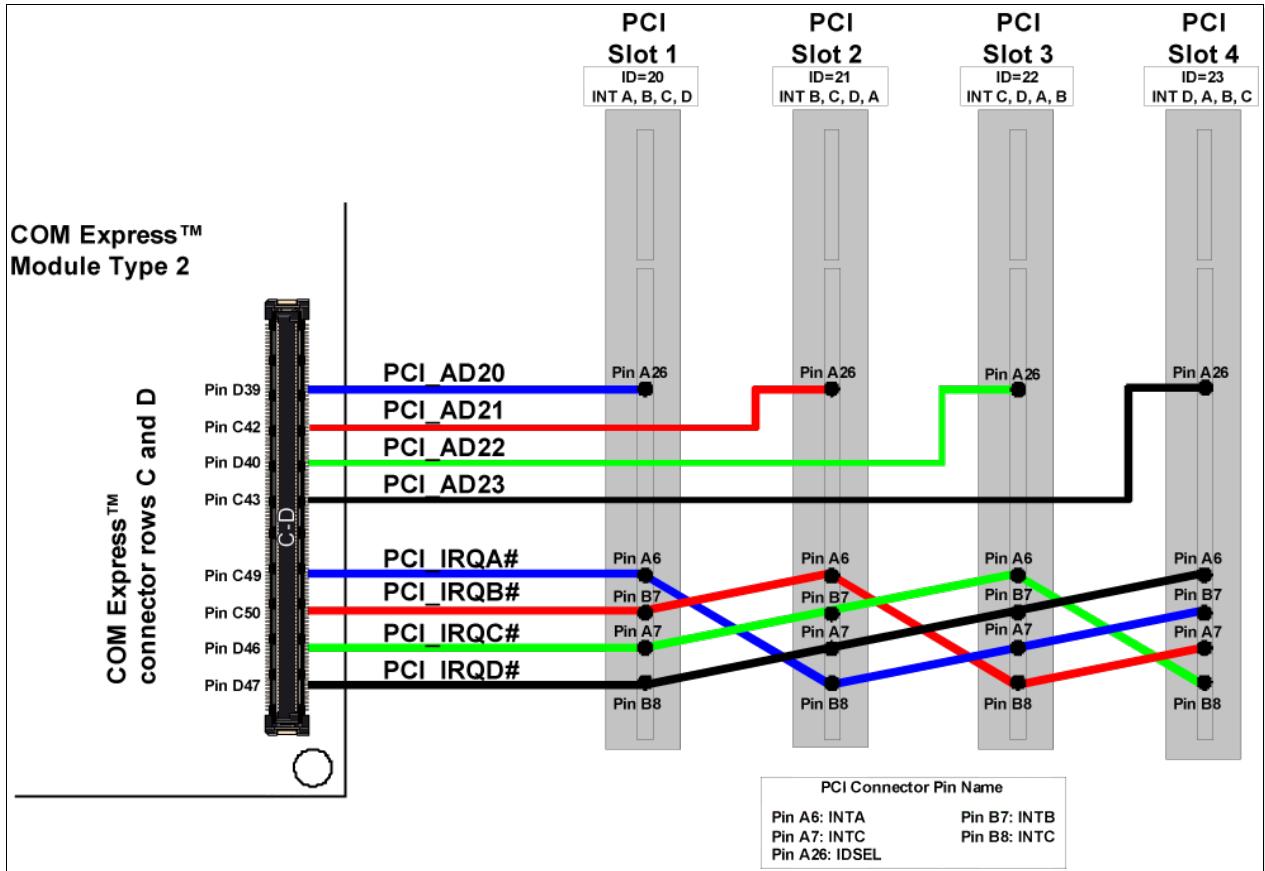
Most of these PCI devices only utilize the interrupt signal 'INTA#'. To distribute the interrupt source of the devices over the interrupt signals 'INTB#', 'INTC#' and 'INTD#', an interrupt cross routing scheme has to be implemented on the COM Express Carrier Board design. Figure 59 above and Table 49 below illustrate the PCI bus interrupt routing for the PCI bus slots 1-4.
Table 49: PCI Bus Interrupt Routing
| Device Signal | Slot / Device 1 | Slot / Device 2 | Slot / Device 3 | Slot / Device 4 |
| IDSEL | PCI_AD[20] | PCI_AD[21] | PCI_AD[22] | PCI_AD[23] |
|
| INTA# | PCI_IRQ[A]# | PCI_IRQ[B]# | PCI_IRQ[C]# | PCI_IRQ[D]# |
| INTB# (if used) | PCI_IRQ[B]# | PCI_IRQ[C]# | PCI_IRQ[D]# | PCI_IRQ[A]# |
| INTC# (if used) | PCI_IRQ[C]# | PCI_IRQ[D]# | PCI_IRQ[A]# | PCI_IRQ[B]# |
| INTC# (if used) | PCI_IRQ[D]# | PCI_IRQ[A]# | PCI_IRQ[B]# | PCI_IRQ[C]# |
Requests and Grants cannot be shared. There should only be a single REQ / GNT pair per device.
# 2.23.2.2. Device-Down Example
Figure 60: PCI Device Down Example; Dual UART
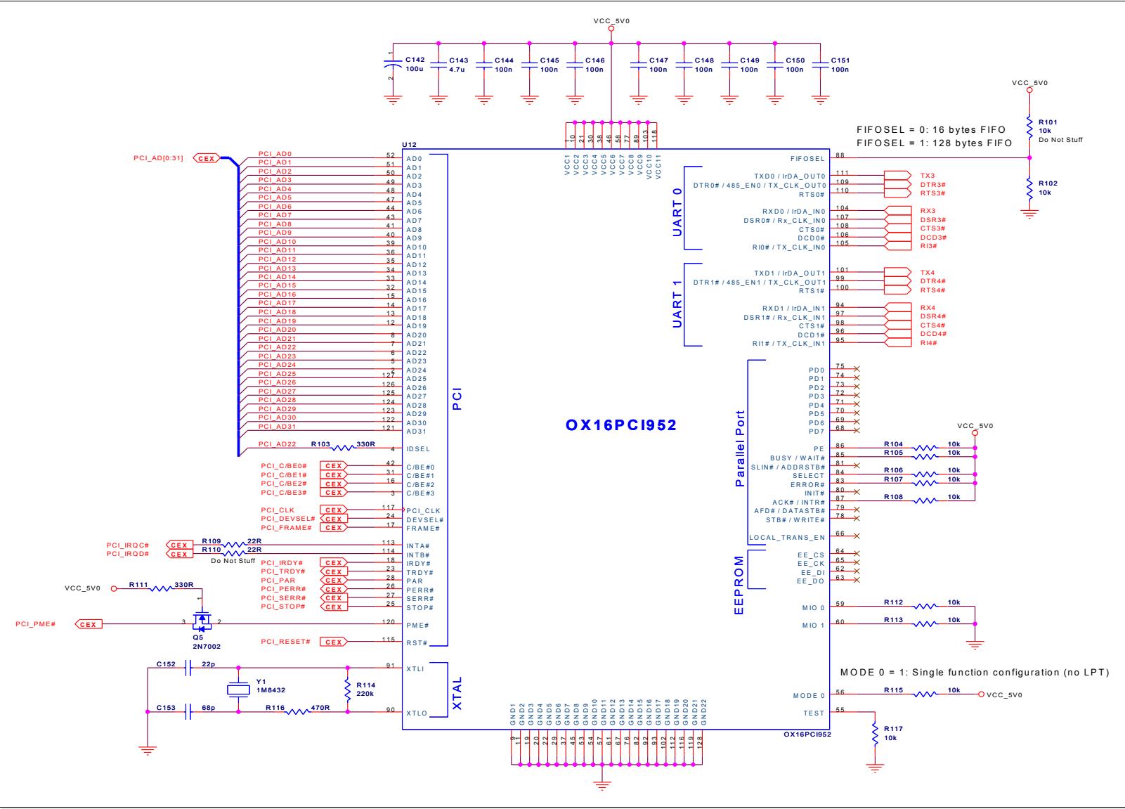
# 2.23.2.3. Device-Down Considerations
# 2.23.2.4. Clock Buffer
The COM Express Specification only supports a single PCI clock signal called 'PCI\_CLK' to be used on the Carrier Board. If there are multiple devices or slots implemented on the Carrier Board, a zero delay clock buffer is required to expand the number of PCI clocks so that each device or each bus slot will be provided with a separate clock signal. Figure 61 below shows an example using the Texas Instruments 'CDCVF2505' zero delay clock buffer providing four output clock signals with spread spectrum compatibility (http://www.ti.com).
Figure 61: PCI Clock Buffer Circuitry
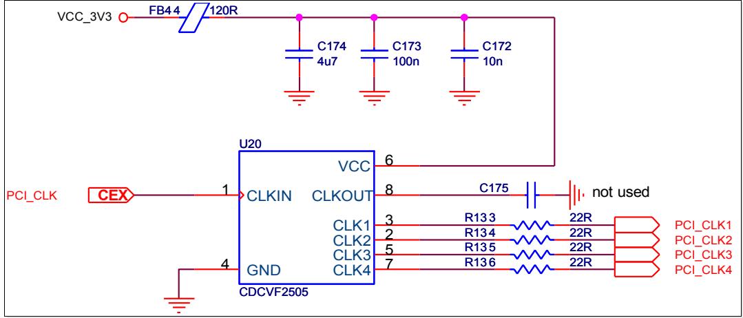
Note: In accordance with the 'PCI Local Bus Specification Revision 2.3', the PCI clock signal requires a rise and fall time (slew rate) within 1V/ns and 4V/ns. The slew rate must be met across the minimum peak-to-peak portion of the clock wave form, which is between 0.66V and 1.98V for 3.3V clock signaling. These parameters are very critical for EMI and must be observed during Carrier Board layout when implementing the PCI Bus.
# 2.23.3. Routing Considerations
# 2.23.3.1. General PCI Signals
Route the PCI bus with 55-Ω, single-ended signals. The bus may be referenced to ground (preferred), or to a well-bypassed power plane, or a combination of the two. Point-to-point (daisy-chain) routing is preferred, although stubs up to 1.5 inches may be acceptable.
See Section 6.6.1. 'PCI Trace Routing Guidelines' on page 191 for a summary of trace routing parameters and guidelines.
# 2.23.3.2. PCI Clock Routing
Particular attention must be paid to the PCI clock routing. The PCI Local Bus specification requires a maximum propagation delay for the clock signals of 10ns within a propagation skew of 2ns @ 33MHz between the several clock signals.
The COM Express Specification allows 1.6ns ± 0.1ns @ 33MHz propagation delay for the PCI clock signal beginning from the Module pin to the destination pin of the PCI device. The propagation delay is dependent on the trace geometries, PCB stack-up and the PCB dielectric constant.
Calculating using a typical propagation delay value of 180ps/inch for an internal layer clock trace of the Carrier Board, a maximum trace length of 8.88 inches is allowed.
The clock trace from the COM Express Module to a PCI bus slot should be 2.5 inches shorter because PCI cards are specified to have 2.5 inches of clock trace length on the card itself.
PCI clock signals should be routed as a single ended trace with a trace impedance of 55Ω. To reduce EMI, a single ground referenced internal layer is recommended. The clock traces should be separated as far as possible from other signal traces.
Refer to Section 6.6.1 'PCI Trace Routing Guidelines' on page 191 below and the 'PCI Local Bus Specification Revision 2.3' to get more information about this subject.
Note: An approximate value for the signal propagation delay per trace length inch can be calculated by using the following formula:
$$
t _ {p r o p.} = \frac {\sqrt {\varepsilon_ {r}} ^ {\prime}}{1 1 . 8} \frac {n s}{i n c h}
$$
${ \pmb \varepsilon } _ { r } ^ { \prime }$ can be determined from the dielectric constant of the PCB that is used by the following approximation. A typical value for the dielectric constant of an FR4 PCB material is $4 . 2 < \varepsilon _ { r } < 4 . 5$ .
For stripline routing: ${ \mathfrak { E } _ { r } } ^ { \prime } { = } { \mathfrak { E } _ { r } }$
For microstrip routing: $\mathfrak { E } _ { r } \ ^ { \prime } = 0 . 4 7 5 \mathfrak { E } _ { r } + 0 . 6 7 \ f o r 2 . 0 { < } \mathfrak { E } _ { r } { < } 6 . 0$
# 2.24. IDE and CompactFlash (PATA)
# 2.24.1. Signal Definitions
Type 2 and 4 COM Express Modules provide a single channel IDE interface supporting two standard IDE hard drives or ATAPI devices with a maximum transfer rate of ATA100 (Ultra-DMA-100 with 100MB/s transfer rate). The corresponding signals can be found on the Module connector rows C and D.
Table 50: Parallel ATA Signal Descriptions
<table>| Signal | Pin | Description | I/O | IDE40 | IDE44 | CF |
| IDE_D0 | D7 | Bidirectional data to / from IDE device. | I/O 3.3V | 17 | 17 | 21 |
| IDE_D1 | C10 | Bidirectional data to / from IDE device. | I/O 3.3V | 15 | 15 | 22 |
| IDE_D2 | C8 | Bidirectional data to / from IDE device. | I/O 3.3V | 13 | 13 | 23 |
| IDE_D3 | C4 | Bidirectional data to / from IDE device. | I/O 3.3V | 11 | 11 | 2 |
| IDE_D4 | D6 | Bidirectional data to / from IDE device. | I/O 3.3V | 9 | 9 | 3 |
| IDE_D5 | D2 | Bidirectional data to / from IDE device. | I/O 3.3V | 7 | 7 | 4 |
| IDE_D6 | C3 | Bidirectional data to / from IDE device. | I/O 3.3V | 5 | 5 | 5 |
| IDE_D7 | C2 | Bidirectional data to / from IDE device. | I/O 3.3V | 3 | 3 | 6 |
| IDE_D8 | C6 | Bidirectional data to / from IDE device. | I/O 3.3V | 4 | 4 | 47 |
| IDE_D9 | C7 | Bidirectional data to / from IDE device. | I/O 3.3V | 6 | 6 | 48 |
| IDE_D10 | D3 | Bidirectional data to / from IDE device. | I/O 3.3V | 8 | 8 | 49 |
| IDE_D11 | D4 | Bidirectional data to / from IDE device. | I/O 3.3V | 10 | 10 | 27 |
| IDE_D12 | D5 | Bidirectional data to / from IDE device. | I/O 3.3V | 12 | 12 | 28 |
| IDE_D13 | C9 | Bidirectional data to / from IDE device. | I/O 3.3V | 14 | 14 | 29 |
| IDE_D14 | C12 | Bidirectional data to / from IDE device. | I/O 3.3V | 16 | 16 | 30 |
| IDE_D15 | C5 | Bidirectional data to / from IDE device. | I/O 3.3V | 18 | 18 | 31 |
| IDE_A[0:2] | D13-D15 | Address lines to IDE device. | O 3.3V | 35, 33, 36 | 35, 33, 36 | 20, 19, 18 |
| IDE_IOW# | D9 | I/O write line to IDE device. | O 3.3V | 23 | 23 | 35 |
| IDE_IOR# | C14 | I/O read line to IDE device. | O 3.3V | 25 | 25 | 34 |
| IDE_REQ | D8 | IDE device DMA request. It is asserted by the IDE device to request a data transfer. | I 3.3V | 21 | 21 | 37 |
| IDE_ACK# | D10 | IDE device DMA acknowledge. | O 3.3V | 29 | 29 | 44 |
| IDE_CS1# | D16 | IDE device chip select for 1F0h to 1FFh range. | O 3.3V | 37 | 37 | 7 |
| IDE_CS3# | D17 | IDE device chip select for 3F0h to 3FFh range. | O 3.3V | 38 | 38 | 32 |
| IDE_IORDY | C13 | IDE device I/O ready input. Pulled low by the IDE device to extend the cycle. | I 3.3V | 27 | 27 | 42 |
| IDE_RESET# | D18 | Reset output to IDE device, active low. | O 3.3V | 1 | 1 | 41 |
| IDE_IRQ | D12 | Interrupt request from IDE device. | I 3.3V | 31 | 31 | 43 |
| IDE_CBLID# | D77 | Input from off-Module hardware indicating the type of IDE cable being used. High indicates a 40-pin cable used for legacy IDE modes. Low indicates that an 80-pin cable with interleaved grounds is used. Such a cable is required for Ultra-DMA 66, 100 modes. | I 3.3V | 34 | 34 | 46 |
| DASP | | | | 39 | 39 | 45 |
| GND | | | | 2, 19, 22, 24, 26, 30, 40 | 2, 19, 22, 24, 26, 30, 40, 43 | 17, 16, 15, 14, 12, 11, 10, 8, 12, 6, 9, 33, 25, 26 39 (master) |
| CSEL | | | | 28 | 28 | 39 |
| N.C. | | | | 20, 32 | 20, 32, 44 | 24, 40, 51, 52, 53, 54, 55, 56 39 (slave) |
| VCC_5V | | | | | 41, 42, | 13, 18, 36 |
# 2.24.2. IDE 40-Pin Header (3.5 Inch Drives)
To interface standard 3.5-inch parallel ATA drives, a standard 2.54mm, two row, 40-pin connector in combination with a ribbon conductor cable is used. For slower drive speeds up to ATA33, a normal 40-pin, 1.27mm-pitch conductor cable is sufficient. Higher transfer rates such as ATA66 and ATA100 require 80-pin conductor cables, where the extra 40 conductors are tied to ground to isolate the adjacent signals for better signal integrity. The 80-pin cable assembly also ties pin 34 (IDE\_CBLID#) on the 40-pin header to GND. If IDE\_CBLID# is sampled low by the Module's BIOS, it assumes that the proper high-speed cable is present and sets up the drive parameters accordingly. Jumper settings on the IDE devices determine Master/Slave configuration. The drive activity LED is driven by the Module's pin A28 (COM Express pin ATA\_ACT#).
Figure 62: Connector type: 40 pin, 2 row 2.54mm grid female

# 2.24.3. IDE 44-Pin Header (2.5 Inch and Low Profile Optical Drives)
To interface standard 2.5-inch parallel ATA drives, as well as low profile optical drives, a standard 2.0mm, two row, 44-pin connector in combination with a 44-conductor ribbon cable is used. For slower drive speeds up to ATA33, a normal 44-conductor, 1.0mm-pitch cable is sufficient. Higher transfer rates such as ATA66 and ATA100 require special handling as ground isolated cables like those commonly used for 3.5” ATA devices do not exist for this interface. Simulation as well as testing should be used to determine if an application specific 44-pin cable interface can support ATA66 and ATA100 speeds. Items to be taken into consideration include cable length, placement in the system, folds and routing. Because 44- conductor cables have no method of indicating their transfer rate capability, IDE\_CBLID# must be controlled on the Carrier Board or by using BIOS setup. For 44-pin ATA devices, the drive activity LED is driven by pin 39 of the header.
# 2.24.4. CompactFlash 50 Pin Header
CompactFlash (CF) cards with DMA capability require that the two signals 'IDE\_REQ' and 'IDE\_ACK#' are routed to the CF card socket on the COM Express Carrier Board. If this is not done then some DMA capable CF cards may not work because they are not designed for non DMA mode. For more information about this subject, refer to the data sheet of the CF card or contact your CF card manufacturer.
CF socket pin 39 (CSEL#) is connected to a jumper to select Master or Slave configuration. If jumpered low, the drive is configured for Master mode. This provides the ability to perform a CompactFlash boot.
# 2.24.5. IDE / CompactFlash Reference Schematics
This reference schematic shows a circuitry implementing an IDE connector and a CF card socket that is DMA capable.
Figure 63: IDE 40 Pin and CompactFlash 50 Pin Connector
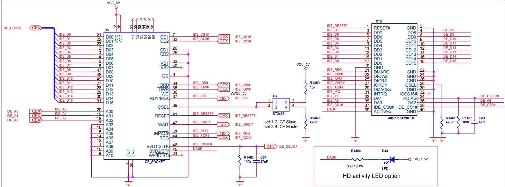
NOTE: by using CF card socket and IDE connector at same time be sure to have just 1 master and 1 slave
# 2.24.6. Routing Considerations
The IDE signals are single-ended signals with a nominal impedance of 55 Ω. See Section 6.6.2. 'IDE Trace Routing Guidelines' on page 192 for more information about routing considerations.
# 3. Power and Reset
# 3.1. General Power requirements
COM Express calls for the Module to be powered by a single 12V power rail, with a +/-5% tolerance. The Mini format Modules are specified in COM.0 Rev. 2.1 to support a power input range of 4.75V to 20.0V. Some vendors offer a wide range input even on Compact and Basic Modules. COM Express Modules may consume significant amounts of power – 25 to 50W is common, and higher levels are allowed by the standard. Close attention must be paid by the Carrier Board designer to ensure adequate power delivery. Details are given in the sections below.
If Suspend functions such as Suspend-to-RAM, Suspend-to-disk, wake on power button press, wake on USB activity, etc. are to be supported, then a 5V Suspend power source must also be provided to the Module. If Suspend functions are not used, the Module VCC\_5V\_SBY pins should be left open. On some Modules, there may be a slight power efficiency advantage to connecting the Module VCC\_5V\_SBY rail to VCC\_5V rather than leaving the Module pin open. Please contact your Module vendor for further details.
Carrier Boards typically require other power rails such as 5V, 3.3V, 3.3V Suspend, etc. These may be derived on the Carrier Board from the 12V and 5V Suspend rails.
# 3.1.1. VCC\_12V Rise Time Caution and Inrush Currents
Direct connection of a COM Express Module to a low impedance supply such as a battery pack may result in excessive inrush currents. The supply to the COM Express Module should be slew limited to limit the input voltage ramp rate. A typical ATX supply ramps at about 2.5 volts per millisecond.
# 3.2. ATX and AT Style Power Control
# 3.2.1. ATX vs AT Supplies
ATX power supplies are in common use in contemporary PCs. ATX supplies have two sets of power rails: a set for normal operation (12V, 5V, 3.3V and -12V) and a separate 5V Suspend rail. The 5V Suspend rail is present whenever the ATX supply has AC input power. The other rails are on only when a control signal from the PC hardware known as PS\_ON# is held low by the motherboard, allowing software control of the power supply. The PC motherboard may implement several mechanisms for controlling the AC power, including a push button switch that switches a low voltage logic signal rather than the AC main power. Other options may be implemented, including the capability to turn on the main power on events such as a keyboard press, mouse activity, etc.
AT power supplies do not have a Suspend rail and do not allow software control of the power supply. An AT supply is on when the supply is connected to the AC main and the power switch that is in series with the AC main input is on. AT supplies are extinct in the commercial PC market, but the term lives on as a reference to a power supply that does not allow software control.
An ATX supply may be converted to AT style operation by simply holding the ATX PS\_ON# input low all the time.
# 3.2.2. Power States
Power states are described by the following terms:
Table 51: Power States
| State | Description | Comment |
| G3 | Mechanical Off | AC power to system is removed by a mechanical switch. System power consumption is near zero – the only power consumption is that of the RTC circuits, which are powered by a backup battery. |
| S5 | Soft Off | System is off except for a small subset that is powered by the 5V Suspend rail. There is no system context preserved. VCC_5V_SBY current consumption is system dependent, and it may be from tens of milliamps up to several hundred milliamps. |
| S4 | Suspend to Disk | System is off except for a small subset that is powered by the 5V Suspend rail. System context is preserved on a non-volatile disk media (that is powered off). VCC_5V_SBY current consumption is system dependent, and it may be from tens of milliamps up to several hundred milliamps. |
| S3 | Suspend to RAM | System is off except for system subset that includes the RAM. Suspend power is provided by the 5V Suspend rail. System context is preserved in the RAM. VCC_5V_SBY current consumption is system dependent, and it may be from several hundred milliamps up to a maximum of 2A. |
| S0 | On | System is on. |
COM Express signals SUS\_S5#, SUS\_S4# and SUS\_S3# have the following behavior in the Power States:
Table 52: Power State Behavior
| State | SUS_S5# | SUS_S4# | SUS_S3# |
| G3 | NA | NA | NA |
| S5 | Low | Low | Low |
| S4 | High | Low | Low |
| S3 | High | High | Low |
| S0 | High | High | High |
# 3.2.3. ATX and AT Power Sequencing Diagrams
A sequence diagram for an ATX style boot from a soft-off state (S5), initiated by a power button press, is shown in Figure 64 below.
A sequence diagram for an AT style boot from the mechanical off state (G3) is shown in Figure 65 below below.
In both cases, the VCC\_12V, VCC\_5V and VCC\_3V3 power lines should rise together in a monotonic ramp with a positive slope only, and their rise time should be limited. Please refer to the ATX specification for more details.
Figure 64: ATX Style Boot – Controlled by Power Button
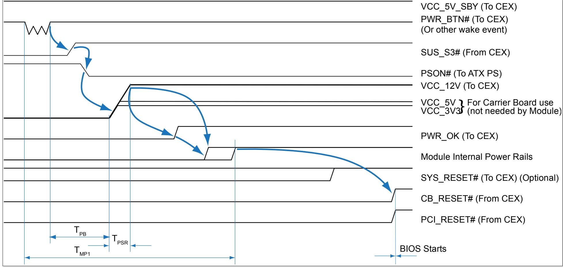
Figure 65: AT Style Power Up Boot
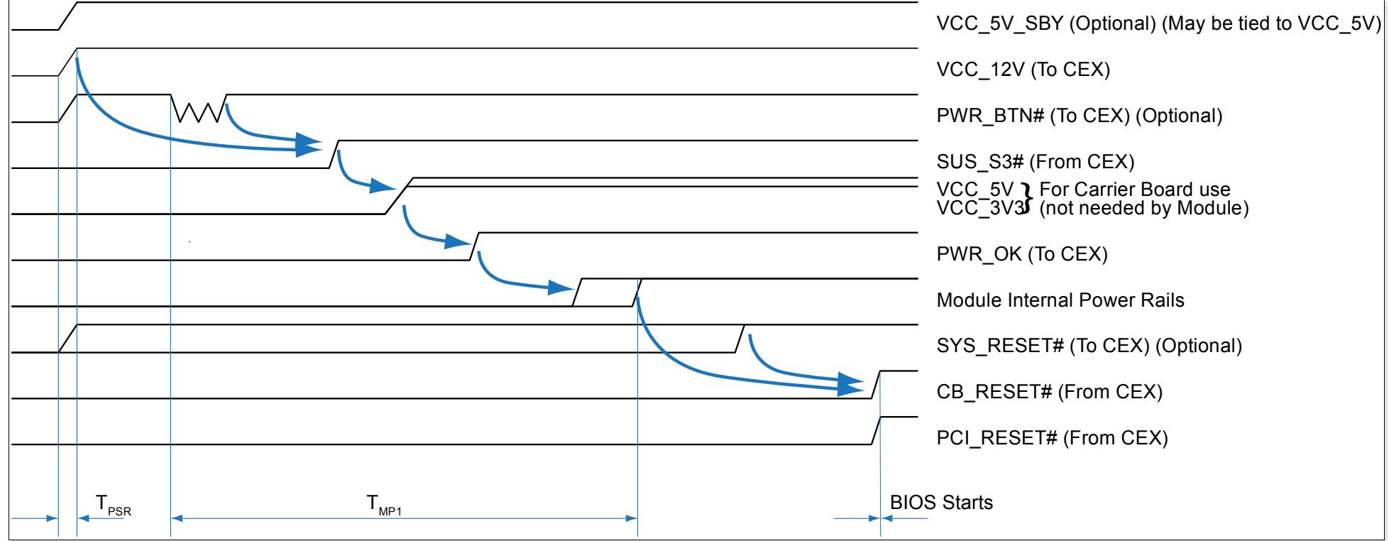
Table 53 below indicates roughly what time ranges can be expected during the boot process, per Figure 64 and 65 above. Check with your Module vendor if more specific information is required.
Table 53: ATX and AT Power Up Timing Values
| Parameter | Min Value | Max Value | Description | Comments |
| TPB | 10ms | 500ms | Push Button Power Switch – time to bring Module chipset out of Suspend mode | Applies only to ATX Style Power Up |
| TPSR | 0.1ms | 20ms | Power Supply Rise Time | |
Notes There is a period of time (TMP1 in Figure 64 and Figure 65 above) during which the Carrier Board circuits have power but the COM Express Module main internal power rails are not up. This is because almost all COM Express internal rails are derived from the external VCC\_12V and there is a non-zero start-up time for the Module internal power supplies.
Carrier Board circuits should not drive any COM Express lines during the TMP1 interval except for those identified in the COM Express Specification as being powered from a Suspend power rail. Almost all such signals are active low. Such signals, if used, should be driven low by open drain Carrier Board circuits to assert them. Pull-ups, if present, should be high value (10K to 100K) and tied to VCC\_5V\_SBY.
The line PWR\_OK may be used during the TMP1 interval to hold off a COM Express Module boot. Sometimes this is done, for example, to allow a Carrier Board device such as an FPGA to be configured before the Module boots.
The deployment of Carrier Board pull-ups on COM Express signals should be kept to a minimum in order to avoid back-driving the COM Express signal pins during this interval. Carrier Board pull-ups on COM Express signal pins are generally not necessary – most signals are pulled up if necessary on the Module.
# 3.2.4. Power Monitoring Circuit Discussion
Contemporary chipsets used in COM Express Modules incorporate a state machine or microcontroller that is powered from a Suspend power rail (i.e. a power rail that is derived from VCC\_5V\_SBY and is on whenever the ATX power supply has incoming AC line power). This state machine or micro-controller operates autonomously from the main CPU on the Module. The function of this state machine or micro-controller is to manage the system power states. It monitors various inputs (e.g. PWRBTN#, WAKE0#, WAKE1#, etc.) that can cause power state changes, and outputs status signals (e.g. SUS\_S5#, SUS\_S4#, SUS\_S3#, SUSPEND#) that can be used by system hardware to control various power supplies and power planes in the system.
# 3.2.5. Power Button
The COM Express PWRBTN# input may be used by Carrier Board hardware to implement ATX style power control. A schematic example of how to do this is given in 3.4.1 'ATX Power Supply' on page 164 below. The COM Express PWRBTN# input is typically de-bounced by the Module chipset.
The behavior of the system after a power failure depends on the Module chipset capabilities and on the Module vendor's hardware and BIOS implementation. With most Modules, the following behaviors may be set by RTC chipset register settings:
Table 54: Power Button States
| State | Description |
| Always On | No Power Button press neededChipset de-assertSUS_S5#,SUS_S4#andSUS_S3#after Suspend rail to chipset is stable |
| Wait For Power Button Press | Chipset remains in Suspend state until power button press is received |
| Last State | If unit was “on” when power was removed, then unit returns to “on” state when power is restored |
# 3.3. Design Considerations for Carrier Boards containing FPGAs/CPLDs
Very often, the Carrier Board will contain custom FPGA or other programmable devices which require the loading of program code before they are usable. The Carrier Board designer needs to take the necessary precautions to ensure that his Carrier Board logic is up and running before the Module starts. Conflicts can occur if the Module is powered on and allowed to run before devices on the Carrier Board are fully programmed and initialized. A typical example is an FPGA which includes a PCIe device. Such devices must be initialized and ready before the chipset on the Module performs link training and before the BIOS code performs enumeration of PCI devices. The Module should therefore be prevented from starting before Carrier Board devices are ready.
One method to achieve this is to delay assertion of the PWR\_OK# signal to the Module until the Carrier Board initialization process has completed. Note that during the phase when the Carrier Board is powered and the Module is not powered there is potential for back drive voltages from the carrier to the Module.
Another possibility is to use the SYS\_RESET# signal to delay Module start-up. However, depending on the Module implementation and the chipset used, SYS\_RESET# may only be a falling edge triggered signal and not a low active signal as was originally intended. In that case, asserting SYS\_RESET# may not hold the Module in the reset state. Also, PCIe link training will occur regardless of the reset signal state for some chipsets.
Please refer to the COM.0 R2.1 specification (Power and System Management section) for more details and check the Module provider’s documentation for their implementations of these signals.
# 3.4. Reference Schematics
# 3.4.1. ATX Power Supply
ATX power supplies are used in millions of desktop PCs and are often used in OEM equipment as well. They are inexpensive and are readily available. An ATX power supply provides more power rails (two separate +12V rails, +5V, +3.3V, -12V and +5V Suspend) than are required by a COM Express Module, but often the Carrier Board and other system components make use of the additional rails.
The following figure shows the ATX power Carrier Board circuitry using a 24 pin ATX main power connector. For systems with power-hungry CPUs or Graphics Cards, two additional +12V power pins may be implemented using an auxiliary 4 pin (2x2) +12V/GND power connector.
Figure 66: AT and ATX Power Supply
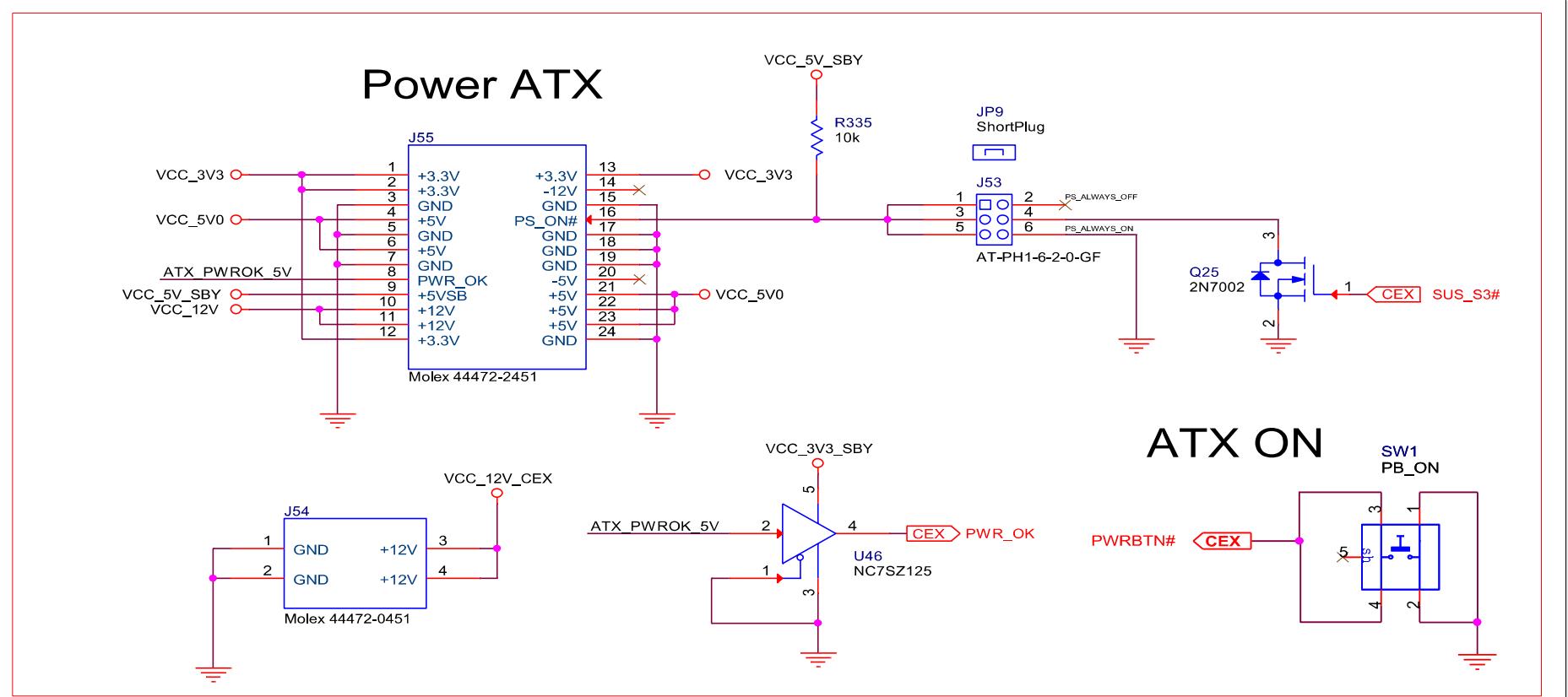

The PWRBTN# signal is an input to the COM Express Module. Switch de-bouncing is done on the Module. The falling edge of the PWRBTN# signal can initiate a state transition from S5 (soft off) to S0 (full on). It may also cause the reverse transition, to S5, if the unit is in one of the 'on' states.
The ATX supply is controlled by the net PS\_ON# in the figure above. The main ATX supply rails are on when PS\_ON# is driven low. To turn the supply off, PS\_ON# can be floated. This net is usually derived from an inverted copy of the COM Express SUS\_S3# signal. Jumper J53 offers the possibility to override this signal with a fixed setup for debugging reasons.
Table 55: ATX Signal Names
| ATX Signal Name | Description |
| PS_ON# | Active-low, TTL-level input to ATX supply that, when low, enables all power rails. If high or floating, all ATX power rails are disabled except for the +5V Suspend rail. |
| PWR_OK | Active-high, TTL-level output signal from the ATX supply that indicates that the +12V, +5V, +3.3V and -12V outputs are all present and OK to use. |
| +12V1DC | +12V power rail for use by all system components except for the CPU, controlled by PS_ON# |
| +12V2DC | +12V power rail for use by the CPU, controlled by PS_ON#. This power rail appears on a separate 2x2 connector for CPU use only. |
| +5VDC | +5V power rail, controlled by PS_ON# |
| +3.3VDC | +3.3V power rail, controlled by PS_ON# |
| -12VDC | -12V power rail, controlled by PS_ON# |
| +5VSB | +5V Suspend power rail, present whenever the ATX supply is connected to its AC power input source. |
| COM | Common return path – usually referred to as “ground” or GND. |
ATX signals are summarized in Table 55 above. Note that there are two separate +12V outputs, +12V1DC and +12V2DC. These are independent +12V sources. Each source is limited to 240W maximum output to meet UL safety requirements. The +12V2DC output is intended for CPU use.
Contemporary ATX supplies have two power connectors on the motherboard:
A 24-pin connector in a 2x12 array that includes all signals in Table 55 above except for +12V2DC.
● A 4-pin connector in a 2x2 array for CPU power that includes +12V2DC and COM only.
Earlier ATX supplies used a 2x10 connector instead of a 2x12. The two connector versions have compatible pin-outs. The 2x10 cable plug may be used with a 2x12 motherboard receptacle as long as pin 1 of the 2x10 cable plug mates with pin 1 of the 2x12 Carrier Board receptacle.
Very early ATX supplies had a single +12V rail, on a 2x10 connector. The 2x2 CPU connector was not present. ATX power supplies are designed for desktop systems, which often have power-hungry CPUs and peripherals. CPUs that require 80W are common. Most Modules use lower-power CPUs, and the ATX supply capacity may be overkill. In particular, two +12V supplies are not necessary for many COM Express Modules.
# 3.4.1.1. Minimum Loads
ATX supplies may not start up if the loading on the +12V, +5V and +3.3V rails is too light. The ATX12V Power Supply Design Guide shows suggested minimum loads in various configurations but does not specify what the minimum loads are. The minimum loads required may vary with different power supply vendors. Experience has shown that a dummy load on the order of at least 400 mA is required on the +5V line in COM Express Carrier Boards that use little or no +5V and are powered from ATX supplies.
# 3.5. Routing Considerations
# 3.5.1. VCC\_12V and GND
The primary consideration for the +12V power input (VCC\_12V) to the Module is that the trace be wide enough to handle the maximum expected load, with plenty of margin. A power plane may be used for VCC\_12V but is not recommended; VCC\_12V should not be used as a reference for high-speed signals, such as PCIe, USB, or even PCI, because there may be switching noise present on VCC\_12V.
A 40W CPU Module can draw over 3.5A on the VCC\_12V pins. Sizing the VCC\_12V delivery trace to handle at least twice the expected load is recommended for good design margin. It is best to keep the Carrier Board VCC\_12 trace short, wide, and away from other parts of the Carrier Board. See the following section for advice on how to size the trace.
If there are layer transitions in the power delivery path, use redundant “power” vias – vias that are sized with larger holes and pads than default vias.
For the GND return, it is best to use a solid, continuous plane, or multiple planes, using the heaviest possible copper.
It is very important to connect all available power and ground pins available on the COM Express Module to the Carrier Board.
# 3.5.2. Copper Trace Sizing and Current Capacity
The current capacity of a PCB trace is proportional to the trace’s cross-sectional area – the product of the trace width and thickness. The trace thickness is proportional to the “weight” of copper used. The copper weight is expressed in ounces per square foot in the United States. Usually people will omit the “per square foot” and just use “ounce” to describe the copper. Copper weights of ½ ounce/ 17μm and sometimes 1 ounce/ 35μm are common for inner layer traces. A copper weight of 1 ounce/ 35μm is common for power planes. A copper weight of ½ ounce/ 17μm results in a thickness of approximately 0.7 mil, and 1 ounce/ 35μm copper yields approximately 1.4 mil. Outer layer traces are usually built with ½ ounce/ 17μm copper, but then are “plated up” with additional conductive material, often yielding an effective copper weight of about 1 ounce/ 35μm. The effective weight of outer layer traces may vary with different PCB processes. Check with your PCB vendor, or play it safe and make conservative assumptions.
Consult sources such as the IPC-2221 for charts that relate copper weight, trace width and tracecurrent capacity at a given temperature rise to the current capability. It is best to assume a conservative trace temperature rise, such as 10° C maximum, when making trace-width decisions. Per the IPC charts, external layer traces can carry significantly more current than internal layer traces, assuming the same base copper weight and the same temperature rise. Approximate current handling capabilities of selected trace widths read off of the IPC-2221 charts are shown in Table 56 below.
Table 56: Approximate Copper Trace Current Capability per IPC-2221 Charts
| Trace Type | Max Current with 10°C Temp Rise | Max Current with 20°C Temp Rise |
| 100 mil wide internal trace 1⁄2 ounce/ 17μm base copper | 1.3 A | 1.8 A |
| 200 mil wide internal trace 1⁄2 ounce/ 17μm base copper | 2.0 A | 3.0 A |
| 400 mil wide internal trace 1⁄2 ounce/ 17μm base copper | 3.5 A | 5.0 A |
| | |
| 100 mil wide internal trace 1 ounce/ 35μm base copper | 2.1 A | 3.0 A |
| 200 mil wide internal trace 1 ounce/ 35μm base copper | 3.5 A | 5.2 A |
| 400 mil wide internal trace 1 ounce/ 35μm base copper | 6.0 A | 8.0 A |
| | |
| 100 mil wide external trace 1⁄2 ounce/ 17μm base copper | 2.4 A | 3.4 A |
| 200 mil wide external trace 1⁄2 ounce/ 17μm base copper | 4.0 A | 5.5 A |
| 400 mil wide external trace 1⁄2 ounce/ 17μm base copper | 7.0 A | 10.0 A |
# 3.5.3. VCC5\_SBY Routing
The +5V Suspend power rail, if used, should be sized to handle 2A. Most, but not all, Modules will use considerably less than 2A for this power rail. Modules with multiple Ethernet channels and wake-on-LAN capability will use more current. The COM Express Specification allows up to 2A on this rail.
# 3.5.4. Power State and Reset Signal Routing
Power state and reset signals are single-ended signals that do not have any particular routing constraints.
To utilize the full functionality of PCI Express devices on the COM Express Carrier Board, some additional supply voltages are necessary besides the standard supply voltages of the ATX power supply. Many PCI Express devices are capable of generating wake up events during Suspend operation; for example an external PCI Express Ethernet device that supports 'Wake On LAN' functionality. Therefore, it is necessary to generate an additional 3.3V Suspend voltage on the Carrier Board to supply such devices during Suspend operation. The voltage regulator must be designed to meet the power requirements of the connected devices.
The PCI Express specification defines maximum power requirements for the different PCI Express connectors and/or devices. The power supply for the Carrier Board must be designed to meet these maximum power requirements. Table 57 below shows the maximum current consumption defined for the different types of PCI Express connectors.
Table 57: PCIe Connector Power and Bulk Decoupling Requirements
| Power Rail | PCIe x1, x4 or x8 Connector | PCIe x16 Connector | ExpressCard Connector | PCIe Mini Card Connector |
| VCC_12V | 2.1A @ 1000uF bulk | 5.5A @ 2000uF bulk | | |
| VCC_3V3 | 3.0A @ 1000uF bulk | 3.0A @ 1000uF bulk | 1.35A | - |
| VCC_3V3_SB | 375mA @ 150uF bulk | 375mA @ 150uF bulk | 275mA | 2.75A |
| VCC_1V5 | | | 750mA | 500mA |
# 3.5.5. Slot Card Supply Decoupling Recommendations
Implementing PCI Express connectors on the Carrier Board requires decoupling of the connector supply voltages to reduce possible voltage drops and to provide an AC return path in a manner consistent with high-speed signaling techniques. Decoupling capacitors should be placed as close as possible to the power pins of the connectors. Table 58 below shows the minimum requirements for power decoupling of the different power pin types of each PCI Express connector type.
Table 58: PCIe High Frequency Decoupling Requirements
| Power Pin Type | PCIe x1, x4 Connector | PCIe x16 Connector | ExpressCard Connector | PCIe Mini Card Connector |
| VCC_12V | 1x 22μF, 2x 100nF | 4x 22uF, 2x 100nF | - | - |
| VCC_3V3 | 1x 22uF, 2x 100nF | 1x 100uF, 2x 100nF | - | - |
| VCC_3V3_SB | 1x 22uF, 2x 100nF | 1x 22uF, 2x 100nF | - | - |
| VCC_1V5 | - | - | - | - |
# 4. BIOS Considerations
# 4.1. Legacy versus Legacy-Free
For the purposes of this document, “legacy” refers to a set of peripherals provided in desktop PCs and associated chipsets that are no longer in production, including PS/2 keyboard and mouse, parallel port (LPT), and UART serial ports. The COM Express standard was created with newer chipsets in mind. As a result, COM Express is “legacy-free”, which means that legacy peripherals are not directly supported by the Module. Such peripherals have been replaced by space-efficient high-speed interfaces such as USB 2.0.
To facilitate the market’s transition toward newer peripherals, the Low Pin Count (LPC) interface was created as a space-efficient replacement for the Industry Standard Architecture (ISA) bus. In addition to firmware devices such as BIOS flash, low-speed super I/O controllers were developed for the LPC bus to fill the gap until the momentum could build for new high-speed-serial-based peripherals.
# 4.2. Super I/O
Within the COM Express modular architecture, super I/O controllers could be placed on Carrier Boards according to unique application requirements. However, LPC super I/O devices are closely coupled to the BIOS firmware that initializes them and performs setup-based interrupt assignments. The BIOS flash generally resides on the COM Express Modules in order for the Modules to be self-booting. This tight coupling of LPC super I/O to the BIOS presents a multitude of problems in a legacy-free modular environment.
Normally the BIOS vendor supplies to the BIOS developer the choice of different super I/O Modules that can be plugged-in at the source level during the BIOS build process. The BIOS super I/O code Modules often require considerable adaptation work by the BIOS developer to be able to be “plugged-in”. The supported super I/O device would be determined by the Module vendor, and other device support would involve a custom BIOS for each super I/O device.
Consequently, PICMG recommends using USB peripherals or PCI or PCI Express super I/O devices on Carrier Boards for customers wishing to use UART serial ports (COM1, COM2, etc.) or other legacy peripherals. Plug-and-play based interrupt assignments are automatic, and drivers initialize devices after the operating system is loaded. A USB keyboard can be used to enter BIOS setup prior to power-on self-test.
PICMG recommends against using LPC super I/O devices on the Carrier Board, as such usage creates BIOS customization requirements and can greatly restrict Module interoperability. PCI, PCI Express, and/or USB devices should be used instead.
PICMG suggests that alternate BIOS firmware support on the Carrier Board as well as port 0x80 implementations are appropriate uses of the LPC interface on the Carrier Board.
# 5. COM Express Module Connectors
# 5.1. Connector Descriptions
A pair of 220-pin COM Express Carrier-Board connectors is available from the vendor in a bridged configuration in which the two 220-pin connectors are held together during assembly by a disposable bridge. The bridge keeps the two connectors aligned, relative to each other, during assembly.
Table 59: COM Express Module Connectors
| Type | Height | Partnumber | Note |
| single connector | 5 mm | Tyco 3-1827253-6Foxconn QT002206-2131-3Hept 401-51101-51 | 220 pos., 0.5mm, Plug |
| connector pair | 5 mm | Tyco 3-1827233-6Foxconn QT002206-2141-3Hept 401-51501-51 | 440 pos., 0.5mm, Plug, with bridge |
| single connector | 8 mm | Tyco 3-6318491-6Foxconn QT002206-4131-3Hept 401-55101-51 | 220 pos., 0.5mm, Plug |
| connector pair | 8 mm | Tyco 3-5353652-6Foxconn QT002206-4141-3Hept 401-55501-51 | 440 pos., 0.5mm, Plug, with bridge |
Please check with your Carrier Board manufacturer to determine if single connectors or connector pairs are preferred.
# Vendorlinks:
TE: http://www.te.com/catalog/products/en?q=com+express
Foxconn: http://nw.foxconn.com/Search/Product\_Details\_Report.asp? P\_Type=Board+to+Board+Connector&P\_Family= Board+to+Board+Connector&P\_Series=Board+to+Board +Connector+0%2E5mm+Pitch&P\_PN=QT002206-2131- 3H&searchTypeID=3
EPT: http://www.ept.de/index.php?colibri-COM-Express
Figure 67: COM Express Carrier Board Connectors
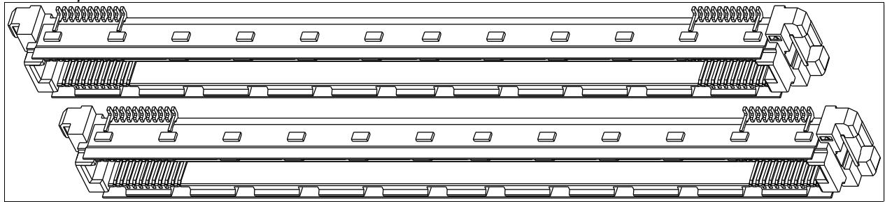
# 5.2. Connector Land Patterns and Alignment
It is extremely important that the designers of Carrier Boards ensure that the COM Express connectors have the proper land patterns and that the connectors are aligned correctly. The land pattern is diagrammed in the COM Express Specification. Connector alignment is ensured if the peg location holes in the PCB connector pattern are in the correct positions (as shown in the land pattern of the COM Express Specification) and if the holes are drilled to the proper size and tolerance by the PCB fabricator.
# 5.3. Connector and Module CAD Symbol Recommendations
The 440-pin COM Express connector should be shown in the Carrier Board CAD system as a single schematic symbol and a single PCB symbol, rather than as a pair of 220-pin symbols. This ensures that the relative position of the two 220-pin connectors remains correct as PCB placement for the Carrier Board is done.
It also is very advantageous to extend this concept to include the COM Express Module outline and the Module mounting holes in the same PCB land pattern. This allows PCB designers to easily move the entire Module around to try placement options without losing the relative positions and orientations of the Module connectors, mounting holes, and Module outline.
# 6. Carrier Board PCB Layout Guidelines
# 6.1. General
# 6.2. PCB Stack-ups
Note Section 6 'Carrier Board PCB Layout Guidelines' assumes a thickness for the carrier PCB to be 0.0625 inches. Other PCB mechanics are possible but the described Stack-ups need to be adapted.
# 6.2.1. Four-Layer Stack-up
Figure 68: Four-Layer Stack-up
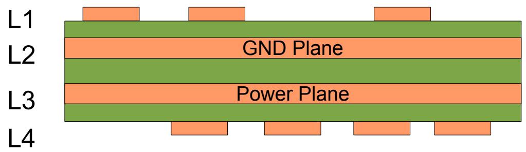
Figure 68 above is an example of a four layer stack-up. Layers L1 and L4 are used for signal routing.
Layers L2 and L3 are used for solid ground and power planes respectively.
Microstrips on Layers 1 and 4 reference ground and power planes on Layers 2 and 3 respectively.
In some cases, it may be advantageous to swap the GND and PWR planes. This allows Layer 4 to be GND referenced. Layer 4 is clear of parts and may be the preferred primary routing layer.
# 6.2.2. Six-Layer Stack-up
Figure 69: Six-Layer Stack-up
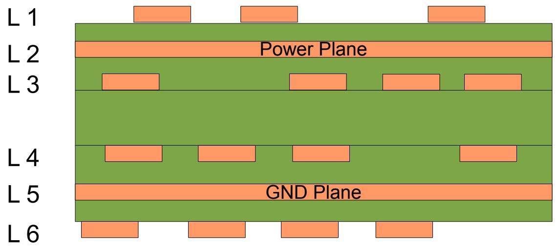
Figure 69 above is an example of a six layer stack-up. Layers L1, L3, L4 and L6 are used for signal-routing. Layers L2 and L5 are power and ground planes respectively.
Microstrips on Layers 1 and 6 reference solid ground and power planes on Layers 2 and 5 respectively.
Inner Layers 3 and 4 are asymmetric striplines that are referenced to planes on Layers 2 and 5.
# 6.2.3. Eight-Layer Stack-up
Figure 70: Eight-Layer Stack-up
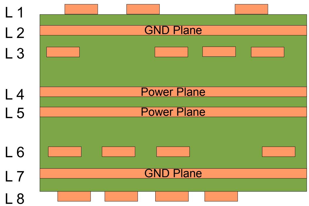
Figure 70 above is an example of an eight layer stack-up. Layers L1, L3, L6 and L8 are used for signal-routing. Layers L2 and L7 are solid ground planes, while L4 and L5 are used for power.
Microstrip Layers 1 and 8 reference solid ground planes on Layers 2 and 7 respectively.
Inner signal Layers 3 and 6 are asymmetric striplines that route differential signals. These signals are referenced to Layers 2 and 7 to meet the characteristic impedance target for these traces.
To reduce coupling to Layers 4 and 5, specify thicker prepreg to increase layer separation.
# 6.3. Trace-Impedance Considerations
Most high-speed interfaces used in an COM Express design for a Carrier Board are differential pairs that need a well-defined and consistent differential and single-ended impedance. The differential pairs should be edge-coupled (i.e. the two lines in the pair are on the same PCB layer, at a consistent spacing to each other). Broadside coupling (in which the two lines in the pair track each other on different layers) is not recommended for mainstream commercial PCB fabrication.
There are two basic structures used for high-speed differential and single-ended signals. The first is known as a “microstrip”, in which a trace or trace pair is referenced to a single ground or power plane.
The outer layers of multi-layer PCBs are microstrips. A diagram of a microstrip cross section is shown in Figure 71: Microstrip Cross Section below.
The second structure is the “stripline”, in which a trace or pair of traces is sandwiched between two reference planes, as shown in Figure 72: Strip Line Cross Section below. If the traces are exactly halfway between the reference planes, then the stripline is said to be symmetric or balanced. Usually the traces are a lot closer to one of the planes than the other (often because there is another orthogonal trace layer, which is not shown in Figure 72: Strip Line Cross Section below). In this case, the striplines are said to be asymmetric or unbalanced. Inner layer traces on multi-layer PCBs are usually asymmetric striplines.
Before proceeding with a Carrier Board layout, designers should decide on a PCB stack-up and on trace parameters, primarily the trace-width and differential-pair spacing. It is quite a bit harder to change the differential impedance of a trace pair after layout work is done than it is to change the impedance of a single-ended signal. That is because (with reference to Figure 71: Microstrip Cross Section below, Figure 72: Strip Line Cross Section below, Table 60 'Trace Parameters' below) the geometric factors that have the biggest impact on the impedance of a single-ended trace are H1 and W1.
Both H1 and W1 can be manipulated slightly by the PCB vendor. The differential impedance of a trace pair depends primarily on H1, W1 and the pair pitch. A PCB vendor can easily manipulate H1 and W1 but changing the pair pitch cannot generally be done at fabrication time. It is more important for the PCB designer and the Project Engineer to determine the routing parameters for differential pairs ahead of time.
Work with a PCB vendor on a suitable board stack-up and do your own homework using a PCBimpedance calculator. An easy to use and comprehensive calculator is available from Polar Instruments (www.polarinstruments.com). Many PCB vendors use software from Polar Instruments for their calculations. Polar Instruments offers an impedance calculator on a lowcost, per-use basis. To find this, search the Web for a “Polar Instruments subscription”.
Alternatively, impedance calculators are included in many PCB layout packages, although these are often incomplete when it comes to differential-pair impedances. There also are quite a few free impedance calculators available on the Web. Most are very basic, but they can be useful.
Figure 71: Microstrip Cross Section
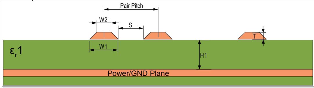
Figure 72: Strip Line Cross Section
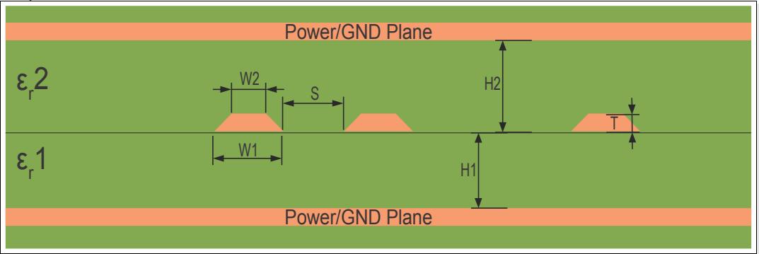
Table 60: Trace Parameters
| Symbol | Definition |
| $\varepsilon_{r}1$ | Dielectric constant of material between the trace and the reference plane. Increasing $\varepsilon_{r}1$ results in a lower trace impedance. |
| $\varepsilon_{r}2$ | Dielectric constant of the material between the $2^{nd}$ reference plane (stripline case only).Usually $\varepsilon_{r}1$ and $\varepsilon_{r}2$ are the same. Increasing $\varepsilon_{r}2$ results in a lower trace impedance. |
| H1 | Distance between the trace lower surface and the closer reference plane.Increasing H1 raises the trace impedance (assuming that H1 is less than H2). |
| H2 | Distance between the trace lower surface and the more distant reference plane (stripline case only).Usually H2 is significantly greater than H1.When this is true, the lower plane shown in the figure is the primary reference plane. Increasing H2 raises the trace impedance. |
| Pair Pitch | The center-to-center spacing between two traces in a differential pair. Increasing the pair pitch raises the differential trace impedance. |
| S | The spacing or gap between two traces in a differential pair. The pair pitch is the sum of S and W1.Increasing S raises the differential trace impedance. |
| T | The thickness of the trace. The thickness of a $\frac{1}{2}$ oz. inner layer trace is about 0.0007 inches. The thickness of a 1 oz. inner layer trace is about 0.0014 inches. Outer layer traces using a given copper weight are thicker, due to plating that is usually done on outer layers. Increasing the trace thickness lowers trace impedance. |
| W1, W2 | W1 is the base thickness of the trace. W2 is the thickness at the top of the trace. The relation between W1 and W2 is called the “etch factor” in the PCB trade. For rough calculations, it can be assumed that W1 = W2. The etch factor is process dependent. W2 is often about 0.001 inches less than W1 for $\frac{1}{2}$ oz inner layer traces; for example, a 5 mil (0.005 inch) nominal trace will be 5-mil wide at the bottom and 4-mil wide at the top. Increasing the trace-width lowers trace impedance. |
# 6.4. Trace-Length Extensions Considerations
High speed differential signals need controlled impedance and according to the maximum loss budget a controlled maximum trace length. In some systems the maximum trace length need to be exceeded on the Carrier Board according to mechanical or system engineering reasons. Trace-length extensions can be done with special signal conditioning chips from vendors like Texas Instruments or Pericom, which are available for USB 3.0, SATA and PCIe.
Figure 73: Trace-length extension with signal conditioning chip
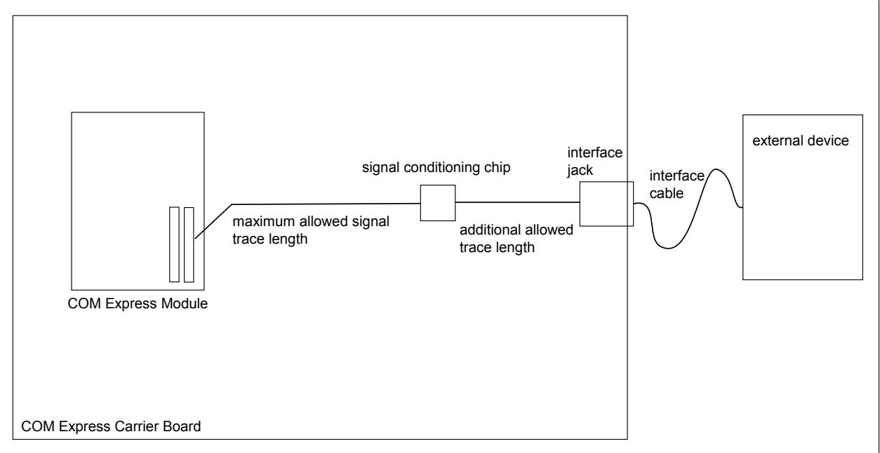
# 6.5. Routing Rules for High-Speed Differential Interfaces
The following is a list of suggestions for designing with high-speed differential signals. This should help implement these interfaces while providing maximum COM Express Carrier Board performance.
● Use controlled impedance PCB traces that match the specified differential impedance.
● Keep the trace lengths of the differential signal pairs as short as possible.
The differential signal pair traces should be trace-length matched and the maximum tracelength mismatch should not exceed the specified values. Match each differential pair per segment.
Maintain parallelism and symmetry between differential signals with the trace spacing needed to achieve the specified differential impedance.
● Maintain phase- and length-matching throughout the whole routing trace.
Maintain maximum possible separation between the differential pairs and any high-speed clocks/periodic signals (CMOS/TTL) and any connector leaving the PCB (such as, I/O connectors, control and signal headers, or power connectors).
Route differential signals on the signal layer nearest to the ground plane using a minimum of vias and corners. This will reduce signal reflections and impedance changes. Use GND stitching vias when changing layers.
It is best to put CMOS/TTL and differential signals on a different layer(s), which should be isolated by the power and ground planes.
Avoid tight bends. When it becomes necessary to turn 90°, use two 45° turns or an arc instead of making a single 90° turn.
Do not route traces under crystals, crystal oscillators, clock synthesizers, magnetic devices or ICs that use, and/or generate, clocks.
Stubs on differential signals should be avoided due to the fact that stubs will cause signal reflections and affect signal quality.
Keep the length of high-speed clock and periodic signal traces that run parallel to high-speed signal lines at a minimum to avoid crosstalk. Based on EMI testing experience, the minimum suggested spacing to clock signals is 50mil.
Use a minimum of 20mil spacing between the differential signal pairs and other signal traces for optimal signal quality. This helps to prevent crosstalk.
Traces should be routed over a continuous GND plane. If this is not possible, a well bypassed VCC plane can be used. Route all traces over continuous planes (GND or VCC) with no interruptions. Avoid crossing over anti-etch if at all possible. Crossing over anti-etch (split planes) increases inductance and radiation levels by forcing a greater loop area.
Figure 74: Layout Considerations
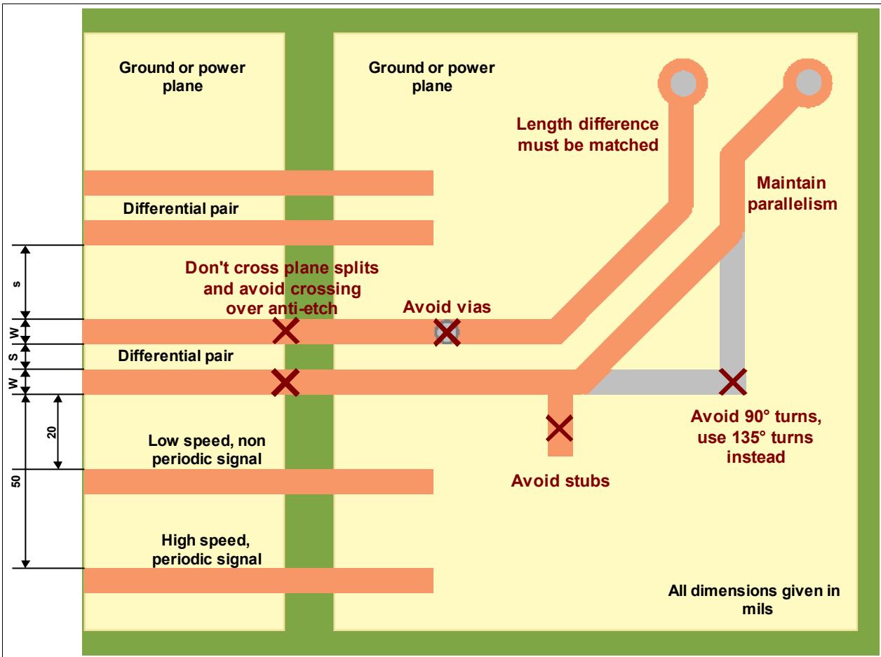
In order to determine the necessary trace width, trace height and spacing needed to fulfill the requirements of the interface specification, it's necessary to use an impedance calculator.
# 6.5.1. PCI Express Trace Routing Guidelines
Table 61: PCI Express Trace Routing Guidelines
| Parameter | PCIe Gen1 | PCIe Gen2 | PCIe Gen3 |
| Symbol Rate / PCIe Lane | 2.5 G Symbols/s | 5.0 G Symbols/s | 8.0 G Symbols/s |
| Maximum signal line length (coupled traces) TX and RX | 21.0 inches | 21.0 inches | 14.0 inches |
| Signal length allowance on the COM Express Carrier Board to PCIe device | 15.85 inches | 15.85 inches | 10.0 inches |
| Signal length allowance on the COM Express Carrier Board to PCIe slot | 9.00 inches | 9.00 inches | 4.0 inches |
| PCI-SIG: Differential impedance recommendation | 100 Ω +/-20% | 85 Ω +/-15% | 85 Ω +/-15% |
| COMCDG Rev. 1.0: Differential impedance recommendation for a GEN1 and GEN2 design | 92 Ω +/-10% | - |
| COMCDG Rev. 2.0: Differential impedance recommendation for new Carrier designs | 85 Ω +/-15% |
| Single-ended Impedance | 55 Ω +/-15% | 50 Ω +/-15% | 50 Ω +/-15% |
| Trace width (W) | PCB stack-up dependent | PCB stack-up dependent | PCB stack-up dependent |
| Spacing between differential pairs (intra-pair) (S) | PCB stack-up dependent | PCB stack-up dependent | PCB stack-up dependent |
| Spacing between RX and TX pairs (inter-pair) (s) | Min. 20mils | Min. 20mils | Min. 20mils |
| Spacing between differential pairs and high-speed periodic signals | Min. 50mils | Min. 50mils | Min. 50mils |
| Spacing between differential pairs and low-speed non periodic signals | Min. 20mils | Min. 20mils | Min. 20mils |
| Length matching between differential pairs (intra-pair) | Max. 5mils | Max. 5mils | Max. 5mils |
| Length matching between RX and TX pairs (inter-pair) | No strict electrical requirements.Keep difference within a 3.0 inch delta to minimize latency. | No strict electrical requirements.Keep difference within a 3.0 inch delta to minimize latency. | No strict electrical requirements.Keep difference within a 3.0 inch delta to minimize latency. |
| Length matching between reference clock differential pairs REFCLK+ and REFCLK-(intra-pair) | Max. 5mils | Max. 5mils | Max. 5mils |
| Length matching between reference clock pairs (inter-pair) | No electrical requirements. | No electrical requirements. | No electrical requirements. |
| Reference plane | GND referenced preferred | GND referenced preferred | GND referenced preferred |
| Spacing from edge of plane | Min. 40mils | Min. 40mils | Min. 40mils |
| Via Usage | Max. 2 vias per TX traceMax. 4 vias per RX trace | Max. 2 vias per TX traceMax. 4 vias per RX trace | Max. 2 vias / TXMax. 4 vias / RX (to device)Max. 2 vias / RX (to slot) |
| AC coupling capacitors | The AC coupling capacitors for the TX lines are incorporated on the COM Express Module.The AC coupling capacitors for RX signal lines have to be implemented on the customer COM Express Carrier Board.Capacitor type: X7R, 100nF +/-10%, 16V, shape 0402. | The AC coupling capacitors for the TX lines are incorporated on the COM Express Module.The AC coupling capacitors for RX signal lines have to be implemented on the customer COM Express Carrier Board.Capacitor type: X7R, 100nF +/-10%, 16V, shape 0402. | The AC coupling capacitors for the TX lines are incorporated on the COM Express Module.The AC coupling capacitors for RX signal lines have to be implemented on customer COM Express Carrier Board.Capacitor type: X7R, 200nF +/-10%, 16V, shape 0402. |
# 6.5.2. USB Trace Routing Guidelines
Table 62: USB Trace Routing Guidelines
| Parameter | Trace Routing |
| Transfer rate / Port | 480 MBit/s |
| Maximum signal line length (coupled traces) | Max. 17.0 inches |
| Signal length used on COM Express Module (including the COM Express connector) | 3.0 inches |
| Signal length allowance for the COM Express Carrier Board | 14.0 inches |
| Differential Impedance | 90 Ω +/-15% |
| Single-ended Impedance | 45 Ω +/-10% |
| Trace width (W) | PCB stack-up dependent |
| Spacing between differential pairs (intra-pair) (S) | PCB stack-up dependent |
| Spacing between pairs-to-pairs (inter-pair) (s) | Min. 20mils |
| Spacing between differential pairs and high-speed periodic signals | Min. 50mils |
| Spacing between differential pairs and low-speed non periodic signals | Min. 20mils |
| Length matching between differential pairs (intra-pair) | 150mils |
| Reference plane | GND referenced preferred |
| Spacing from edge of plane | Min. 40mils |
| Via Usage | Try to minimize number of vias |
# 6.5.3. USB 3.0 Trace Routing Guidelines
Table 63: USB 3.0 Trace Routing Guidelines
| Parameter | Trace Routing |
| Transfer rate / Port | 5.0 GBit/s |
| Maximum signal line length (coupled traces) | 7.5 inches |
| Signal length used on COM Express Module (including the COM Express connector) | 3.0 inches |
| Signal length allowance for the COM Express Carrier Board | 4.5 inches |
| Differential Impedance | 85 Ω +/-10% |
| Single-ended Impedance | 50 Ω +/-15% |
| Trace width (W) | PCB stack-up dependent |
| Spacing between differential pairs (intra-pair) (S) | PCB stack-up dependent |
| Spacing between pairs-to-pairs (inter-pair) (s) | Min. 15mils |
| Spacing between differential pairs and high-speed periodic signals | Min. 15mils |
| Spacing between differential pairs and low-speed non periodic signals | Min. 20mils |
| Length matching between differential pairs (intra-pair) | Max. 5mils |
| Reference plane | Ground |
| Spacing from edge of plane | Min. 40mils |
| Via Usage | Max. 3 vias per differential signal trace |
# 6.5.4. PEG Trace Routing Guidelines
Please refer to Section 6.5.1. 'PCI Express Trace Routing Guidelines' on page 182
Note The COM Express specification does not define different trace routing rules for PEG and PCI Express lanes. Newer chipsets feature low power modes for the PEG signals. In order to ensure compatibility it's recommended to keep the PEG signal lines as short as possible. A max of $\pmb { 5 } ^ { \prime \prime }$ to the carrier device down and $4 ^ { y }$ to a carrier slot is advisable.
# 6.5.5. SDVO Trace Routing Guidelines
Table 64: SDVO Trace Routing Guidelines
| Parameter | Trace Routing |
| Transfer Rate / SDVO Lane | Up to 2.0 GBit/s |
| Maximum signal line length (coupled traces) | 7 inches |
| Signal length used on COM Express Module (including the Carrier Board connector) | 2 inches |
| Signal length allowance for the COM Express Carrier Board | 5 inches to SDVO device |
| Differential Impedance | 100 Ω +/-20% |
| Single-ended Impedance | 55 Ω +/-15% |
| Trace width (W) | PCB stack-up dependent |
| Spacing between differential pairs (intra-pair) (S) | PCB stack-up dependent |
| Spacing between pairs-to-pair | Min. 20mils |
| Spacing between differential pairs and high-speed periodic signals | Min. 50mils |
| Spacing between differential pairs and low-speed non periodic signals | Min. 20mils |
| Length matching between differential pairs (intra-pair) | Max. 5mils |
| Length matching between differential pairs (inter-pair) | Keep difference within a 2.0 inch delta. |
| Length matching between differential signal pair and differential clock pair | Max. 5mils |
| Spacing from edge of plane | Min. 40mils |
| Via Usage | Max. 4 vias per differential signal trace |
| AC coupling capacitors | AC coupling capacitors on the signals 'SDVO_INT+' and 'SDVOINT-' have to be implemented on the customer COM Express Carrier Board, if the device is directly located on the Carrier Board. When using a slot at the Carrier Board the capacitors are located at the addon card.Capacitor type: X7R, 100nF +/-10%, 16V, shape 0402. |
# 6.5.6. DisplayPort Trace Routing Guidelines
Table 65: DisplayPort Trace Routing Guidelines
| Parameter | Trace Routing |
| Transfer Rate | Max. 5.4 GBit/s |
| Maximum signal line length (coupled traces) | 7.2 inches |
| Signal length used on COM Express Module (including the Carrier Board connector) | 4.0 inches |
| Signal length allowance for the COM Express Carrier Board | 3.2 inches |
| Differential Impedance | 85 Ω +/-10% |
| Single-ended Impedance | 50 Ω +/-15% |
| Trace width (W) | PCB stack-up dependent |
| Spacing between differential pairs (intra-pair) (S) | PCB stack-up dependent |
| Spacing between pairs-to-pair | Min. 15mils |
| Spacing between differential pairs and high-speed periodic signals | Min. 15mils |
| Spacing between differential pairs and low-speed non periodic signals | Min. 15mils |
| Length matching between differential pairs (intra-pair) | Max. 5mils |
| Length matching between differential pairs (inter-pair) | Max 1 inch |
| Spacing from edge of plane | Min. 40mils |
| Via Usage | Max. 2 |
| AC coupling capacitors | 100nF |
# 6.5.7. LAN Trace Routing Guidelines
Table 66: LAN Trace Routing Guidelines
| Parameter | Trace Routing |
| Signal length allowance for the COM Express Carrier Board | 5.0 inches from the COM Express Module to the magnetics Module |
| Maximum signal length between isolation magnetics Module and RJ45 connector on the Carrier Board | 1.0 inch |
| Differential Impedance | 95 Ω +/-20% |
| Single-ended Impedance | 55 Ω +/-15% |
| Trace width (W) | PCB stack-up dependent |
| Spacing between differential pairs (intra-pair) (S) | PCB stack-up dependent |
| Spacing between RX and TX pairs (inter-pair) (s) | Min. 50mils |
| Spacing between differential pairs and high-speed periodic signals | Min. 300mils |
| Spacing between differential pairs and low-speed non periodic signals | Min. 100mils |
| Length matching between differential pairs (intra-pair) | Max. 5mils |
| Length matching between RX and TX pairs (inter-pair) | Max. 30mils |
| Spacing between digital ground and analog ground plane (between the magnetics Module and RJ45 connector) | Min. 60mils |
| Spacing from edge of plane | Min. 40mils |
| Via Usage | Max. of 2 vias on TX pathMax. of 2 vias on RX path |
# 6.5.8. Serial ATA Trace Routing Guidelines
Table 67: Serial ATA Trace Routing Guidelines
| Parameter | Trace Routing |
| Transfer Rate | Up to 6.0 GBit/s |
| Maximum signal line length (coupled traces) | 5.0 inches on PCB (COM Express Module and Carrier Board. The length of the SATA cable is specified between 0 and 40 inches) |
| Signal length used on COM Express Module (including the COM Express Carrier Board connector) | 2 inches |
| Signal length available for the COM Express Carrier Board | 3 inches, a redriver may be necessary for GEN3 signaling rates |
| Differential Impedance | 85 Ω +/-20% |
| Single-ended Impedance | 50 Ω +/-15% |
| Trace width (W) | PCB stack-up dependent |
| Spacing between differential pairs (intra-pair) (S) | PCB stack-up dependent |
| Spacing between RX and TX pairs (inter-pair) (s) | Min. 20mils |
| Spacing between differential pairs and high-speed periodic signals | Min. 50mils |
| Spacing between differential pairs and low-speed non periodic signals | Min. 20mils |
| Length matching between differential pairs (intra-pair) | Max. 5mils |
| Length matching between RX and TX pairs (inter-pair) | No strict length-matching requirements. Route the signals as directly as possible. |
| Spacing from edge of plane | Min. 40mils |
| Via Usage | A maximum of 2 vias is recommended. |
| AC Coupling capacitors | The AC coupling capacitors for the TX and RX lines are incorporated on the COM Express Module. |
# 6.5.9. LVDS Trace Routing Guidelines
Table 68: LVDS Trace Routing Guidelines
| Parameter | Trace Routing |
| Maximum signal line length to the LVDS connector (coupled traces) | 8.75 inches |
| Signal length used on COM Express Module (including the COM Express Carrier Board connector) | 2.0 inches |
| Signal length to the LVDS connector available for the COM Express Carrier Board | 6.75 inches |
| Differential Impedance | 100 Ω +/-20% |
| Single-ended Impedance | 55 Ω +/-15% |
| Trace width (W) | PCB stack-up dependent |
| Spacing between differential pair signals (intra-pair) (S) | PCB stack-up dependent |
| Spacing between pair to pairs (inter-pair) (s) | Min. 20mils |
| Spacing between differential pairs and high-speed periodic signals | Min. 20mils |
| Spacing between differential pairs and low-speed non periodic signals | Min. 20mils |
| Length matching between differential pairs (intra-pair) | +/- 20mils |
| Length matching between clock and data pairs (inter-pair) | +/- 20mils |
| Length matching between data pairs (inter-pair) | +/- 40mils |
| Spacing from edge of plane | +/- 40mils |
| Reference plane | GND referenced preferred |
| Via Usage | Max. of 2 vias per line |
# 6.6. Routing Rules for Single Ended Interfaces
The following is a list of suggestions for designing with single ended signals. This should help implement these interfaces while providing maximum COM Express Carrier Board performance.
● Do not route traces under crystals, crystal oscillators, clock synthesizers, magnetic devices or ICs that use or generate clocks.
● Avoid tight bends. When it becomes necessary to turn 90°, use two 45° turns or an arc instead of making a single 90° turn.
● Stubs on signals should be avoided due to the fact that stubs will cause signal reflections and affect signal quality.
Keep the length of high-speed clock and periodic signal traces that run parallel to high-speed signal lines at a minimum to avoid crosstalk. Based on EMI testing experience, the minimum suggested spacing to clock signals is 50mil.
Route all traces over continuous planes with no interruptions (ground reference preferred). Avoid crossing over anti-etch if at all possible. Crossing over anti-etch (split planes) increases inductance and radiation levels by forcing a greater loop area.
● Route digital power and signal traces over the digital ground plane.
Position the bypassing and decoupling capacitors close to the IC pins with wide traces to reduce impedance.
# 6.6.1. PCI Trace Routing Guidelines
Table 69: PCI Trace Routing Guidelines
| Parameter | Trace Routing |
| Transfer Rate @ 33MHz | 132 MB/sec |
| Maximum data and control signal length allowance for the COM Express Carrier Board. | 10 inches |
| Maximum clock signal length allowance for the COM Express Carrier Board. | 8.88 inches |
| Single-ended Impedance | 55 Ω +/-15% |
| Trace width (W) | PCB stack-up dependent |
| Spacing between signals (inter-signal) (S) | PCB stack-up dependent |
| Length matching between single ended signals | Max. 200mils |
| Length matching between clock signals | Max. 200mils |
| Spacing from edge of plane | Min. 40mils |
| Reference plane | GND referenced preferred |
| Via Usage | Try to minimize number of vias |
| Decoupling capacitors for each PCI slot. | Min. 1x22μF, 2x 100nF @ VCC 5VMin. 2x22μF, 4x 100nF @ VCC 3.3VMin. 1x22μF, 2x 100nF @ +12V (if used)Min. 1x22μF, 2x 100nF @ -12V (if used)The decoupling capacitors for the power rails should be placed as close as possible to the slot power pins, connected with wide traces. |
# 6.6.2. IDE Trace Routing Guidelines
Table 70: IDE Trace Routing Guidelines
| Parameter | Trace Routing |
| Maximum Transfer Rate @ ATA100 | 100 MB/sec |
| Maximum length allowance for signals on the COM Express Carrier Board @ ATA100. | 7.0 inches |
| Single-ended Impedance | 55 Ω +/-15% |
| Trace width (W) | PCB stack-up dependent |
| Spacing between signals (inter-signal) (S) | PCB stack-up dependent |
| Length matching between strobe and data signals | Max. 450mils |
| Length matching between data signals | Max. 200mils |
| Length matching between strobe signals 'IDE_IOR' and 'IDE_IOW'. | Max. 100mils |
| Spacing from edge of plane | Min. 40mils |
| Reference plane | GND referenced preferred |
| Via Usage | Try to minimize number of vias |
# 6.6.3. LPC Trace Routing Guidelines
Table 71: LPC Trace Routing Guidelines
| Parameter | Trace Routing |
| Transfer Rate @ 33MHz | 16 MBit/s |
| Maximum data and control signal length allowance for the COM Express Carrier Board | 15.0 inches |
| Maximum clock signal length allowance for the COM Express Carrier Board | 8.88 inches |
| Single-ended Impedance | 55 Ω +/-15% |
| Trace width (W) | PCB stack-up dependent |
| Spacing between signals (inter-signal) (S) | PCB stack-up dependent |
| Length matching between single ended signals | Max. 200mils |
| Length matching between clock signals | Max. 200mils |
| Spacing from edge of plane | Min. 40mils |
| Reference plane | GND referenced preferred |
| Via Usage | Try to minimize number of vias |
# 7. Mechanical Considerations
# 7.1. Form Factors
The COM Express specification describes 4 different sized COM Express Modules. The Mini (55x84 mm), Compact (95x95 mm), Basic (95x125 mm) and the Extended (110x155 mm) Modules. A Carrier Board can be designed to handle more than one Module size by placing Carrier Board mounting holes at the appropriate locations for each Module size that will be supported. For example, a Carrier Board designed for Basic-sized Modules could provide additionally the one mounting hole, unique for Compact-sized Modules, to allow that size. The necessary standoffs can then be populated if applicable.
Figure 75: Mechanical comparison of available COM Express Form Factors
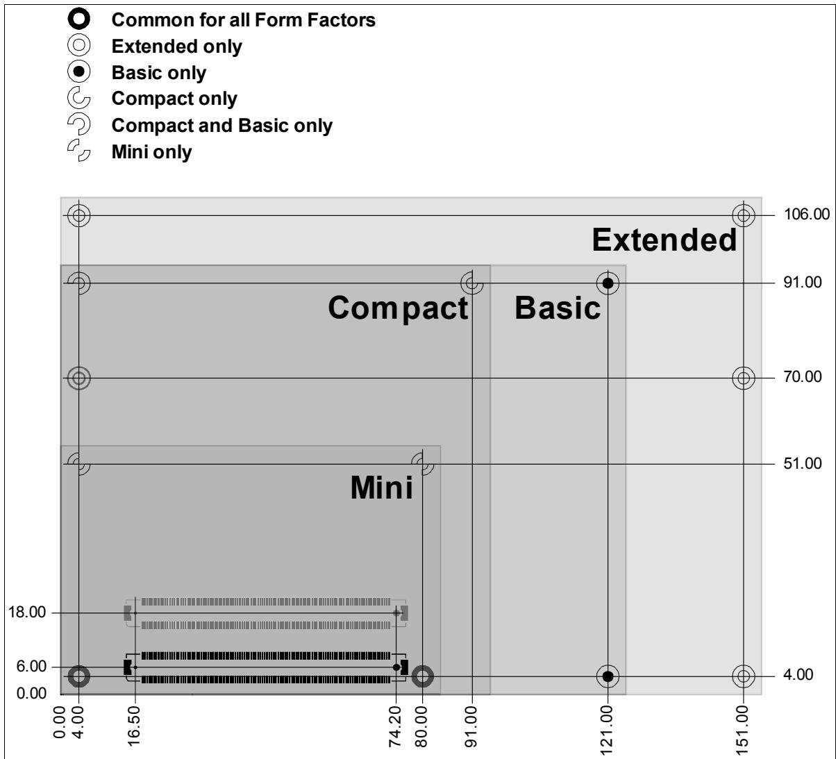
All dimensions are shown in millimeters.
# 7.2. Heatspreader
An important factor for each system integration is the thermal design. The heatspreader acts as a thermal coupling device to the Module. Usually It is a 3mm thick aluminum plate.
The heatspreader is thermally coupled to the CPU via a thermal gap filler and on some Modules it may also be thermally coupled to other heat generating components with the use of additional thermal gap fillers.
Although the heatspreader is the thermal interface where most of the heat generated by the Module is dissipated, it is not to be considered as a heatsink. It has been designed to be used as a thermal interface between the Module and the application specific thermal solution. The application specific thermal solution may use heatsinks with fans, and/or heat pipes, which can be attached to the heatspreader. Some thermal solutions may also require that the heatspreader is attached directly to the systems chassis therefore using the whole chassis as a heat dissipater.
The main mechanical mounting solutions for systems based on COM Express Modules have proven to be the 'top-mounting' and 'bottom-mounting' solutions. The decision as to which solution will be used is determined by the mechanical construction and the cooling solution of the customer's system. There are two variants of the heatspreader, one for each mounting possibility. One version has threaded standoffs and the other has non-threaded standoffs (bore hole). The following sections describe these two common mounting possibilities and the additional components (standoffs, screws, etc...) that are necessary to implement the respective solution.
The examples shown in the following Sections 7.2.1 'Top mounting' and 7.2.2. 'Bottom mounting' are for heatspreader thermal solutions only. Other types of thermal solutions are possible that might require other mounting methods.
# 7.2.1. Top mounting
For top mounting heatspreaders with non-threaded standoffs (bore hole) are used.
This variant of the heatspreader was designed to be used in a system where the heatspreader screws need to be inserted from the top side of the complete assembly. In this case the threads for securing the screws are in the Carrier Board's standoffs. This is the reason why the heatspreader must have non-threaded (bore hole) standoffs.
Figure 76: Complete assembly using non-threaded (bore hole) heatspreader
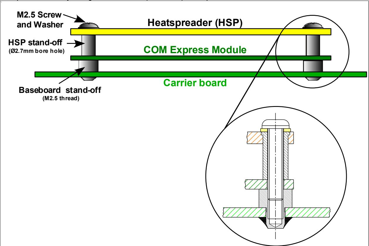
Note The torque specification for heatspreader screws is 0.5 Nm.
Caution Do not use a threaded heatspreader together with threaded Carrier Board standoffs. The combination of the two threads may be staggered, which could lead to stripping or cross-threading of the threads in either the standoffs of the heatspreader or Carrier Board.
# 7.2.2. Bottom mounting
Heatspreaders with threaded standoffs are used for bottom-mounting solutions.
This variant of the heatspreader has been designed to be used in systems where the heatspreader screws need to be inserted from the bottom side of the complete assembly. For this solution a heatspreader version with threaded standoffs must be used. In this case, the standoffs used on the Carrier Board are not threaded.
Figure 77: Complete assembly using threaded heatspreader
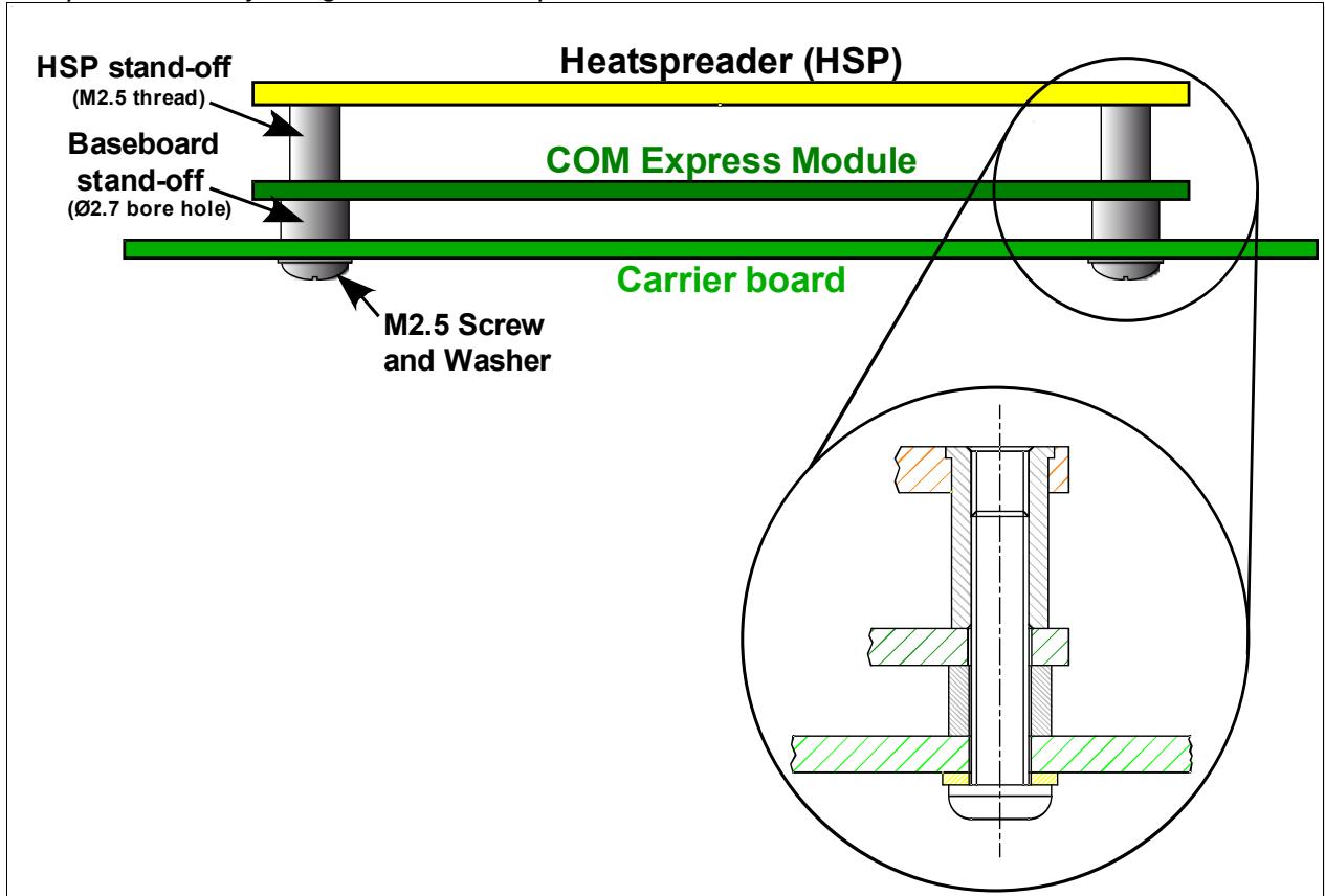
Note The torque specification for heatspreader screws is 0.5 Nm.
Caution Do not use a threaded heatspreader together with threaded Carrier Board standoffs. The combination of the two threads may be staggered, which could lead to stripping of the threads in either the standoffs of the heatspreader or Carrier Board.
# 7.2.3. Materials
Independently from the above mentioned mounting methods the material from the tables below is required to mount a COM Express Module to a Carrier Board.
Table 72: Heatspreader mounting material needed (5mm connectors at the Carrier Board)
| Component | Quantity | Comment |
| M2.5 x 16mm screw $^{1}$ | 5 | Recessed raised cheese head screw with point, galvanized with metric thread M2.5 and 16mm length DIN7985 / ISO7045 |
| Washer 2.7mm | 5 | Plain washer galvanized for M2.5 DIN433 / ISO7092 |
Table 73: Heatspreader mounting material needed (8mm connectors at the Carrier Board)
| Component | Quantity | Comment |
| M2.5 x 19mm screw | 5 | Recessed raised cheese head screw with point, galvanized with metric thread M2.5 and 19mm length DIN7985 / ISO7045 |
| Washer 2.7mm | 5 | Plain washer galvanized for M2.5 DIN433 / ISO7092 |
Table 74: Carrier Board standoffs
| Component | Mounting Type | Comment |
| 5mm, press in, M2.5 | Top | EFCO ECM00593-L, www.efcotec.com/product.asp?pid=102 |
| 5mm, press in, ∅2.7mm | Bottom | EFCO ECM00592-L, www.efcotec.com/product.asp?pid=102 |
| 5mm, solder, M2.5 | Top | EFCO ECM00530-L, www.efcotec.com/product.asp?pid=102 |
| 8mm, press in, M2.5 | Top | EFCO ECM00594L, www.efcotec.com/product.asp?pid=102 |
| 8mm, press in, ∅2.7mm | Bottom | EFCO ECM00588-L, www.efcotec.com/product.asp?pid=102 |
| 5mm, solder, M2.5 | Top | EFCO ECM00579-L, www.efcotec.com/product.asp?pid=102 |
| 5mm spacer | Bottom | misc. |
| 8mm spacer | Bottom | misc. |
| 5mm spacer + nut | Top | misc. |
| 8mm spacer + nut | Top | misc. |
# 8. Applicable Documents and Standards
# 8.1. Technology Specifications
Table 75: Reference specifications
| Specification | Description | Link |
| 1000BASE T | IEEE standard 802.3ab 1000BASE T Ethernet | www.ieee.org/portal/site |
| AC'97 | Audio Codec '97 Component Specification, Version 2.3 | download.intel.com/support/motherboards/de sktop/sb/ac97_r23.pdf |
| ACPI | Advanced Configuration and Power Interface Specification | www.acpi.info |
| ATA | ANSI NCITS 397-2005: AT Attachment with Packet Interface - 7 (ATA/ATAPI-7) | www.ansi.orgwww.t13.org |
| ATX power | ATX power supply design guide | www.intel.com |
| CAN | Controller Area Network | www.iso.org |
| CF-Card | CF+ and CompactFlash Specification Copyright © Compact Flash Association. | www.compactflash.org |
| COM Express | PICMG® COM Express ModuleTM Base Specification | www.picmg.org |
| COM.0 | PICMG COM.0 R2.1, "COM Express Module Base Specification", May 14, 2012 | www.picmg.org |
| DDC | Enhanced Display Data Channel Specification (DDC) | www.vesa.org |
| DisplayID | DisplayID | www.vesa.org |
| DVI | Digital Visual Interface, Digital Display Working Group | www.ddwg.org |
| EAPI | Embedded Application Programming Interface | www.picmg.org |
| EDID | Extended Display Identification Data Standard (EDIDTM) | www.vesa.org |
| EEEP | Embedded EEPROM Specification | www.picmg.org |
| ExpressCard | ExpressCard Standard | www.expresscard.org |
| HDA | High Definition Audio Specification | www.intel.com/standards/hdaudio |
| I2C | The I2C Bus Specification | www.nxp.com |
| IEEE 802.3-2008 | IEEE Standard for Information technology, Telecommunications and information exchange between systems—Local and metropolitan area networks—Specific requirements – Part 3: Carrier Sense Multiple Access with Collision Detection (CSMA/CD) Access Method and Physical Layer Specifications | www.ieee.org |
| LPC | Low Pin Count Interface Specification (LPC) | www.intel.com/design/chipsets/industry/lpc.htm |
| LVDS | Open LVDS Display Interface (Open LDI) Specification, Copyright © National Semiconductor | www.national.com |
| LVDS | LVDS Owner's Manual | www.national.com |
| LVDS | ANSI/TIA/EIA-644-A-2001: Electrical Characteristics of Low Voltage Differential Signaling (LVDS) Interface Circuits, January 1, 2001. | www.ansi.org |
| OBD-II | On-Board Diagnostics 2ndgeneration | www.sae.org |
| PATA | Parallel ATA [IDE] | www.t13.org |
| PCI | PCI Local Bus Specification | www.pcisig.com/specifications |
| PCI Express | PCI Express Base Specification, PCI Special Interest Group. All rights reserved | www.pcisig.com |
| PCI Express | PCI Express Base Specification | www.pcisig.com/specifications |
| PCI Express | Mobile Graphics Low-Power Addendum to the PCI Express Base Specification | www.pcisig.com |
| PCI Express Card | PCI Express Card Electromechanical Specification | www.pcisig.com/specifications |
| PCI Express Mini Card | PCI Express Mini Card Electromechanical Specification, PCI Special Interest Group | www.pcisig.com |
| SATA | Serial ATA: High Speed Serialized AT Attachment, Copyright © APT Technologies, Inc., Dell Computer Corporation, Intel Corporation, Maxtor Corporation, Seagate Technology LLC. All rights reserved | www.sata-io.org |
| SATA | Serial ATA Specification | www.serialata.org |
| SDVO | Intel NDA is required | |
| SMBUS | System Management Bus (SMBUS) Specification, Copyright © Duracell, Inc., Energizer Power Systems, Inc., Fujitsu, Ltd., Intel Corporation, Linear Technology Inc., Maxim Integrated Products, Mitsubishi Electric Semiconductor Company, PowerSmart, Inc., Toshiba Battery Co. Ltd., Unitrode Corporation, USAR Systems, Inc. All rights reserved | www.smbus.org |
| Smart Battery | Smart Battery Data Specification | www.sbs-forum.org |
| USB | Universal Serial Bus Specification, Copyright © Compaq Computer Corporation, Hewlett-Packard Company, Intel Corporation, Lucent Technologies Inc, Microsoft Corporation, NEC Corporation, Koninklijke Philips Electronics N.V. All rights reserved | www.usb.org |
| USB 3.0 | Universal Serial Bus Revision 3.0 Specification | www.usb.org |
| USB | USB Power Delivery Specification | www.poweredusb.org |
# 8.2. Regulatory Specifications
FCC Rules Part 15 Class B devices
EN 61000-4-2 Personnel Electrostatic Discharge Immunity Testing
UL1642 Standard for Lithium Batteries
# 8.3. Useful books
Table 76: Useful books
| Title | Author | Note |
| PCI Express System Architecture | Ravi Budruk, Don Anderson, Tom Shanley | www.mindshare.com |
| PCI System Architecture (4th Edition) | Tom Shanley, Don Anderson | www.mindshare.com |
| Universal Serial Bus System Architecture | Don Anderson | www.mindshare.com |
| SATA Storage Technology | Don Anderson | www.mindshare.com |
| Protected Mode Software Architecture (The PC System Architecture Series) | Tom Shanley | www.mindshare.com |
| The Unabridged Pentium 4 | Tom Shanley | www.mindshare.com |
| Building the Power-Efficient PC: A Developer's Guide to ACPI Power Management, First Edition | Jerzy Kolinski, Ram Chary, Andrew Henroid, and Barry Press | Intel Press, 2002, ISBN 0-9702846-8-3 |
| Hardware Bible | Winn L. Rosch | SAMS, 1997, 0-672-30954-8 |
| The Indispensable PC Hardware Book | Hans-Peter Messmer | Addison-Wesley, 1994, ISBN 0-201-62424-9 |
| The PC Handbook: For Engineers, Programmers, and Other Serious PC Users, Sixth Edition | John P. Choisser and John O. Foster | Annabooks, 1997, ISBN 0-929392-36-1 |
| PC Hardware in a Nutshell, 3rd Edition | Robert Bruce Thompson and Barbara Fritchman Thompson | O'Reilly, 2003, ISBN 0-596-00513-X |
| PCI & PCI-X Hardware and Software Architecture & Design, Fifth Edition | Edward Solari and George Willse | Annabooks, Intel Press, 2001, ISBN 0-929392-63-9 |
| PCI System Architecture | Tom Shanley and Don Anderson | Addison-Wesley, 2000, ISBN 0-201-30974-2 |
| PCI Express Electrical Interconnect Design: Practical Solutions for Board-level Integration and Validation, First Edition | Dave Coleman, Scott Gardiner, Mohamad Kolberhdari, and Stephen Peters | Intel Press, 2005, ISBN 0-9743649-9-1 |
| Introduction to PCI Express: A Hardware and Software Developer's Guide, First Edition | Adam Wilen, Justin Schade, and Ron Thornburg | Intel Press, 2003, ISBN 0-9702846-9-1 |
| Serial ATA Storage Architecture and Applications, First Edition | Knut Grimsrud and Hubbert Smith | Intel Press, 2003, ISBN 0-9717861-8-6 |
| USB Design by Example, A Practical Guide to Building I/O Devices, Second Edition | John Hyde | Intel Press, ISBN 0-9702846-5-9 |
| Universal Serial Bus System Architecture, Second Edition | Don Anderson and Dave Dzatko | Mindshare, Inc., ISBN 0-201-30975-0 |
| Printed Circuits Handbook, Fourth Edition | Clyde F. Coombs Jr. | McGraw-Hill, 1996, ISBN 0-07-012754-9 |
| High Speed Signal Propagation, First Edition | Howard Johnson and Martin Graham | Prentice Hall, 2003, ISBN 0-13-084408-X |
| High Speed Digital Design: A Handbook of Black Magic, First Edition | Howard Johnson | Prentice Hall, ISBN: 0133957241 |
| C Programmer's Guide to Serial Communications, Second Edition | Joe Campbell | SAMS, 1987, ISBN 0-672-22584-0 |
| The Programmer's PC Sourcebook, Second Edition | Thom Hogan | Microsoft Press, 1991, ISBN 1-55615-321-X |
| The Undocumented PC, A Programmer's Guide to I/O, CPUs, and Fixed Memory Areas | Frank van Gilluwe | Addison-Wesley, 1997, ISBN 0-201-47950-8 |
| VHDL Modeling for Digital Design Synthesis | Yu-Chin Hsu, Kevin F. Tsai, Jessie T. Liu and Eric S. Lin | Kluwer Academic Publishers, 1995, ISBN: 0-7923-9597-2 |
# 9. Appendix A: Deprecated Features
The following content was removed from the main part of this document because it is no longer part of the COM.0 Rev. 2.1 specification. It is kept here in the appendix for reference.
# 9.1. TV-Out
# 9.1.1. Signal Definitions
TV-Out signals are defined on COM Express connector row B. Up to 3 individual digital-toanalog converter (DAC) channels are available on the connector. The following video formats may be supported:
Composite Video: All color, brightness, blanking, and sync information are encoded onto a single signal.
S-Video: (Separated Video) video signal with two components, brightness (luma) and color (chroma). This is also known as Y-C video.
Component Video: A video signal that consists of three components. The components may be RGB or may be encoded using other component encoding schemes such as YUV, YCbCr, and YPbPr.
A COM Express Module may support all, some, or none of these formats. Within these formats, there are different encoding schemes that may be used. The most widely used encoding schemes are NTSC (used primarily in North America) and PAL (used primarily in Europe)
Which format and encoding options are available are Module and vendor dependent. Only one output mode can be used at any given time.
Table 77: TV-Out Signal Definitions
| Signal | Pin | Description | I/O | Comment |
| TV_DAC_A | B97 | TV-DAC channel A output supporting:Composite video: CVBSComponent video: Chrominance (Pb)S-Video: not used | O Analog | Analog output |
| TV_DAC_B | B98 | TV-DAC channel B output supporting:Composite video: not usedComponent video: Luminance (Y)S-Video: Luminance (Y) | O Analog | Analog output |
| TV_DAC_C | B99 | TV-DAC channel C output supporting:Composite video: not usedComponent: Chrominance (Pr)S-Video: Chrominance (C) | O Analog | Analog output |
# 9.1.2. TV-Out Connector
Figure 78: TV-Out Video Connector (combined S-Video and Composite)
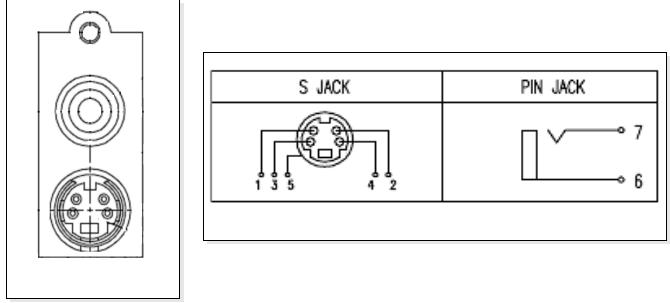
Table 78: TV-Out Connector Pin-out
| Pin | Signal | Description | Pin | Signal | Description |
| 1 | Chrominance (C) | S-Video Chrominance Analog Signal (C) | 2 | Luminance (Y) | S-Video Luminance Analog Signal (Y) |
| 3 | GND (C) | Analog Ground for Chrominance (C) | 4 | GND (Y) | Analog Ground Luminance (Y) |
| 5 | GND | Analog Ground | 6 | GND | Analog Ground |
| 7 | Composite | Composite Video Output | |
# 9.1.3. TV-Out Reference Schematics
All signals along the left edge of the figure below are sourced directly from the COM Express Module. No additional pull-ups or terminations beyond what is shown in the figure are required.
The 150 Ω termination to ground is important both for signal integrity and to establish the correct DC level on the line. All components shown in this figure should be placed close to the Carrier Board connector shown in the figure.
Figure 79: TV-Out Reference Schematics
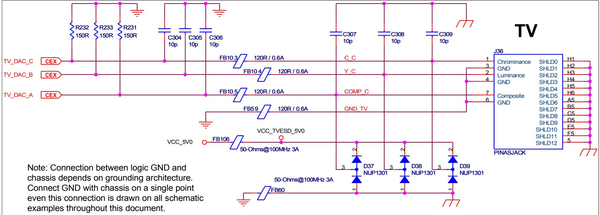
# 9.1.4. Routing Considerations
At least 30mils of spacing should be used for the routing between each TV-DAC channel to prevent crosstalk between the TV-DAC signals. The maximum trace length distance of the TV-DAC signals between the COM Express connector and the 150Ω ±1% termination resistor should be within 12 inches. This distance should be routed with a 50Ω trace impedance.
# 9.1.5. Signal Termination
Each of the TV-DAC channels should have a 150Ω ±1% pull-down termination resistor connected from the TV-DAC output of the COM Express Module to the Carrier Board ground. This termination resistor should be placed as close as possible to the TV-Out connector on the Carrier Board. A second 150Ω ±1% termination resistor exists on the COM Express Module itself.
# 9.1.6. Video Filter
There should be a PI-filter placed on each TV-DAC channel output to reduce high-frequency noise and EMI. The PI-filter consists of two 10pF capacitors with a 120Ω @ 30Mhz ferrite bead between them. It is recommended to place the PI-filters and the termination resistors as close as possible to the TV-Out connector on the Carrier Board. The PI-filters should be separated from each other by at least 50mils or more in order to minimize crosstalk between the TV-DAC channels.
# 9.1.7. ESD Protection
ESD clamp diodes are required for each TV-DAC channel. These low capacitance clamp diodes should be placed as near as possible to the TV-Out connector on the COM Express Carrier Board between +5V supply voltage and ground.
# 9.2. LPC Firmware Hub
An example of a Carrier Board Firmware Hub (FWH) implementation is shown in Figure 80: LPC Firmware Hub below. Use the FWH to store and execute BIOS code.
A feature of the COM Express specification is the inclusion of the BIOS\_DISABLE# pin. If this pin is pulled low on the Carrier Board, then the BIOS on the Module is disabled. The BIOS can instead reside on the Carrier Board LPC or PCI buses. This is useful in some regulatory situations in which it is required that regulatory technicians remove the BIOS, check its integrity, and replace it. There is usually room on a Carrier Board for a socketed BIOS, whereas the Module BIOS is often a surface-mount device. The use of this feature is illustrated in the example below.
Figure 80: LPC Firmware Hub
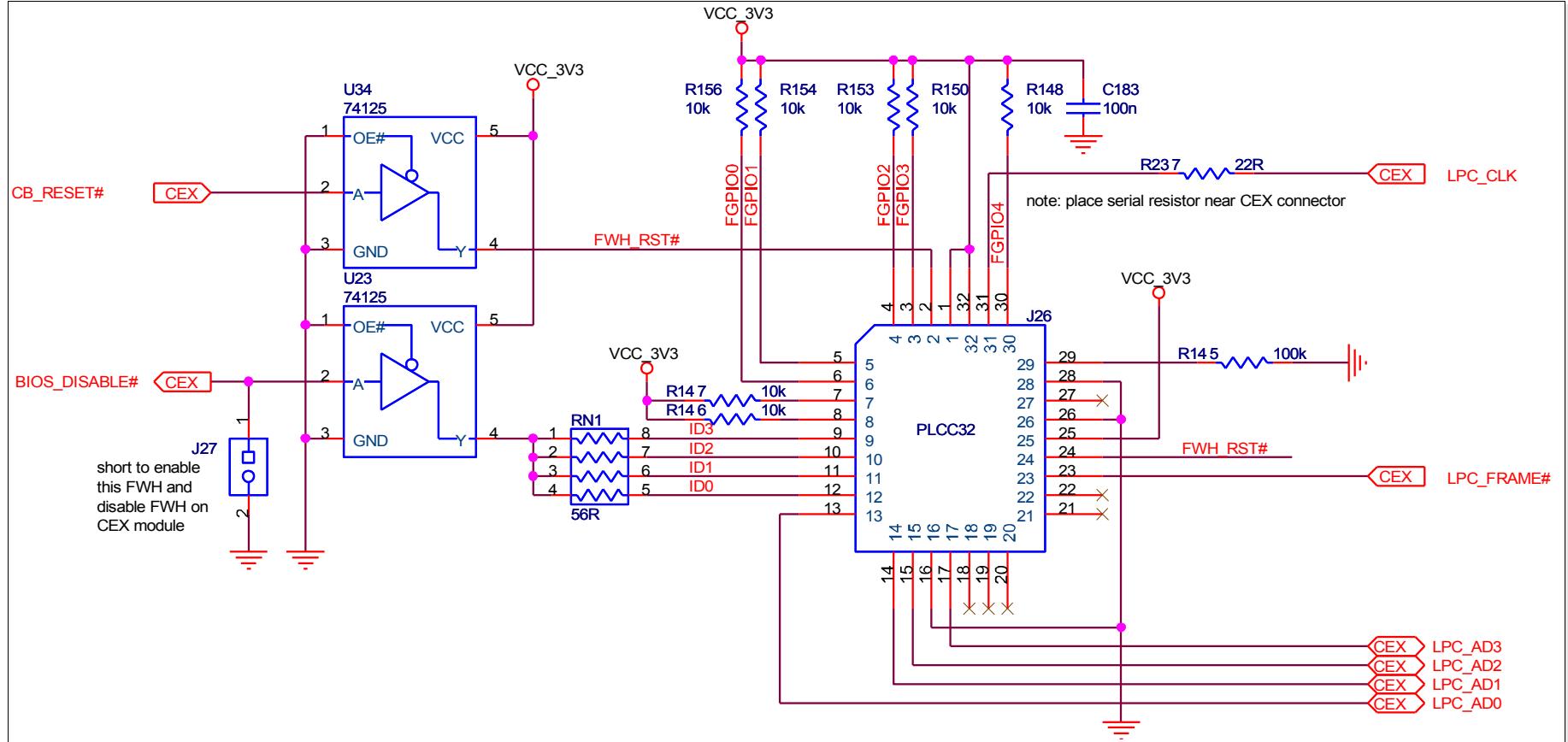
The BIOS device shown in Figure 80: LPC Firmware Hub above is a SST SST49LF008A Firmware Hub in a 32-pin PLCC package. The socket used is a 32-pin PLCC socket, AMP/Tyco 822498-1. This is a surface-mount socket, and PCBs can be laid out such that the socket or the FWH itself is soldered to the Carrier Board.
The FWH is connected to the system via the LPC interface. Data and address information are carried on the LPC\_AD[0:3] lines. LPC\_FRAME# indicates the start of a new frame.
FWH pins 2 (RST#) and 24 (INIT#) reset the FWH. These pins are logically combined together internally on the FWH, and a low on either pin will reset the FWH.
FWH pins 6, 5, 4, 3, 30 – (FGPI [0:4]) are general-purpose inputs that may be read by system software. They should be tied to a valid logic level.
FWH pin 7 ( WP#) enables write protection for main block sectors when it is pulled low. If pulled high, hardware write protection is disabled. FWH pin 8 (TBL# ) enables write protection for the top block sector when pulled low.
FWH pins 12,11,10, 9 – (ID[0:3]) are ID pins that allow multiple FWH parts (up to 16) to be used. By convention, in Intel x86-based systems, the boot device is FWH number 0. To boot from the Carrier Board FWH, the Module BIOS\_DISABLE# pin must be low (to disable the Module BIOS) and the Carrier Board FWH ID[0:3] pins (pins 12,11,10,9) must be low (to enable it as the boot device). If jumper J27 in Figure 80: LPC Firmware Hub above is installed, the Module BIOS is disabled, and the Carrier Board FWH may be used as a boot device.
FWH pin 29 configures the FWH into one of two modes: if high, the FWH is in the Programmer configuration. If low, it is in the firmware hub configuration. For normal operation on a Carrier Board, this pin should be tied low.
FWH pin 31 is the clock input. The clock source is the LPC\_CLK signal from the COM Express Module.
FWH pin 2 – RST# supports Chip Reset. The LPC\_RESET# signal from the COM Express Module drives the reset. The pin functions the same as INIT# above.
# 10. Appendix B: Sourcecode for Port 80 Decoder
```txt
-- IO80 catcher for LPC bus.
-- File: LPC_IOW80_1.1.VHD
-- Revision: 1.1
-- Author: Eric Leonard (partially based on Nicolas Gonthier's T3001)
-- Subsequent modifications by:
-- Detlef Herbst and Travis Evans - 08/10/05
-- Decode only I/O writes to 80h
-- Features:
-- - I/O 80 access only (internally decoded)
-- - No support for read, only write.
-- - All signals synchronous to LPC clock
-- Notes:
-- - Unless otherwise noted, all signals are active high.
-- - Suffix "n" indicate active low logic.
--
-- - Successfully implemented on Brownsville baseboard with Seven Segment
-- - display P/N SA39-11 (common Anode - Low turns on segment) from Kingbright
-- Related documents:
-- - Low Pin Count (LPC) Interface Specification, Revision 1.0 (sept 1997)
```
library IEEE; use IEEE.std\_logic\_1164.all;
```vhdl
entity LPC_IOW80 is port (
lclk: in std_logic; -- LPC: 33MHz clock (rising edge)
lframe_n: in std_logic; -- LPC: frame, active low
lreset_n:in std_logic; -- LPC: reset, active low
lad: in std_logic_vector(3 downto 0); -- LPC: multiplexed bus
seven_seg_L: out std_logic_vector(7 downto 0); -- SSeg Data output
seven_seg_H: out std_logic_vector(7 downto 0) -- SSeg Data output
);
end LPC_IOW80;
```
architecture RTL of LPC\_IOW80 is
```txt
type LPC_State_Type is (
IDLE, -- Waiting for a start condition
START, -- Start condition detected
WADDN3, -- I/O write address nibble 3 (A15..A12)
WADDN2, -- I/O write address nibble 2 (A11..A8)
WADDN1, -- I/O write address nibble 1 (A7..A4)
WADDN0, -- I/O write address nibble 0 (A3-A0)
WDATN1, -- I/O write data nibble 0 (D7..D4)
WDATN0, -- I/O write data nibble 1 (D3..D0)
WHTAR0, -- I/O write host turn around phase 0
WHTAR1, -- I/O write host turn around phase 1
WSYNC, -- I/O write sync
WPTAR ); -- I/O write peripheral turn around
```
signal LPC\_State: LPC\_State\_Type;
```txt
signal lframe_nreg: std_logic; -- LPC frame register
signal lad_rin: std_logic_vector(lad'range); -- LPC input registers
signal W_Data: std_logic_vector(7 downto 0); -- LPC input Post Code
```
begin
```vhdl
-- LPC bidirectional pins definition.
--
-- Input register to get some timing margin
P_input_register: process(lclk)
begin
if (lclk'event and lclk='1') then
lad_rin <= lad;
lframe_nreg <= lframe_n;
end if;
end process;
```
-- LPC state machine
-- LPC\_State value is actually one clock cycle late.
P\_LPC\_StatMachine: process(lclk)
begin
if (lclk'event and lclk='1') then
-- Synchronous reset
if (lreset_n = '0') then
LPC_State <= IDLE;
W_Data(7 downto 0) <= "00000000"; -- init. both displays to all on
else
case LPC_State is
-- Looking for a START condition
when IDLE =>
if (lframe_nreg = '0') and (lad_rin = "0000") then
LPC_State <= START; -- START condition detected
end if;
-- Skip extra cycles on START frame
-- (can be many clock cycles)
-- and then, check for I/O write transaction
when START =>
if (lframe_nreg = '0') then -- frame still asserted
if (lad_rin /= "0000") then
LPC_State <= IDLE; -- unsupported start code
end if;
else
if (lad_rin(3 downto 1) = "001") then
LPC_State <= WADDN3; -- I/O write detected
else
LPC_State <= IDLE; -- unsupported command
end if;
end if;
-- ----
-- I/O write transaction processing
-- ----
when WADDN3 => -- Write Data Address Nibble 3
-- Find next state
if (lframe_nreg = '0') or (lad_rin /= "0000") then
LPC_State <= IDLE; -- abort cycle, bad frame
-- or address mismatch
else
LPC_State <= WADDN2;
end if;
when WADDN2 => -- Write Data Address Nibble 2
-- Find next state
if (lframe_nreg = '0') or (lad_rin /= "0000") then
LPC_State <= IDLE; -- abort cycle, bad frame
-- or address mismatch
else
LPC_State <= WADDN1;
end if;
when WADDN1 => -- Write Data Address Nibble 1
-- Find next state
if (lframe_nreg = '0') or (lad_rin /= "1000") then
LPC_State <= IDLE; -- abort cycle, bad frame
-- or address mismatch
else
LPC_State <= WADDN0;
end if;
when WADDN0 => -- Write Data Address Nibble 0
-- Find next state
if (lframe_nreg = '0') or (lad_rin /= "0000") then
```txt
LPC_State <= IDLE; -- abort cycle, bad frame -- or address mismatch
```
```txt
else
```
```txt
-- Write address valid. Subsequent Data displays.
```
```txt
LPC_State <= WDATN0;
-- first data nibble
```
```txt
-- Next state will get
```
```txt
t
```
```txt
end if;
```
```txt
when WDATN0 => -- Data LSN (Least Significant Nibble) is -- sent first
```
```txt
W_Data(3 downto 0) <= lad_rin; -- latch data (LSN)
if (lframe_nreg = '1') then
```
LPC_State <= WDATN1; $\neg\neg\neg$ -- Next state gets -- 2nd data nibble
```txt
else
```
```txt
LPC State <= IDLE;
```
```txt
end if;
```
```txt
when WDATN1 => -- Data MSN (Most Significant Nibble)
W_Data(7 downto 4) <= lad_rin; -- latch data (MSN)
if (lframe_nreg = '1') then
LPC_State <= WHTAR0;
else
LPC_State <= IDLE;
end if;
```
```txt
when WHTAR0 => -- Write Data Turn Around Cycle 0
```
```txt
if (lframe_nreg = '1') and (lad_rin = "1111") then
LPC_State <= WHTAR1;
else
LPC_State <= IDLE;
end if;
```
```txt
when WHTAR1 => -- Write Data Turn Around Cycle 1
```
```txt
if (lframe_nreg = '1') then
LPC_State <= WSYNC;
else
LPC_State <= IDLE;
end if;
```
```txt
when WSYNC => -- Write Data Sync Cycle
```
```txt
-- Note: No device to respond with a synch at I/O addr
```
```txt
-- 080h. Therefore bus should time out and abort.
```
```txt
-- State ==> to IDLE
```
```txt
if (lframe_nreg = '1') then
LPC_State <= WPTAR;
else
LPC_State <= IDLE;
end if;
```
```txt
when WPTAR => -- Write Data Final Turn Around Cycle -- (not needed -- see WSYNC)
```
```txt
LPC_State <= IDLE; -- I/O write cycle end
```
```txt
when others =>
```
```txt
LPC_State <= IDLE; -- all other cases
```
```rust
end case;
```
```txt
end if;
```
```vhdl
end if;
end process;
```
```txt
P_sseg_decode: process(lclk)
begin
```
```txt
-- decode section for 7 seg displays
```
```txt
if (lclk'event and lclk='1') then
```
```txt
case W_Data(7 downto 4) is
```
```txt
-- Most sig digit for display
```
```perl
when "0000" => seven_seg_H <= "00000011"; -- Hex 03 displays a 0
when "0001" => seven_seg_H <= "10011111";-- Hex 9f displays a 1
when "0010" => seven_seg_H <= "00100101"; -- Hex 25 displays a 2
when "0011" => seven_seg_H <= "00001101"; -- Hex 0d displays a 3
when "0100" => seven_seg_H <= "10011001"; -- Hex 99 displays a 4
when "0101" => seven_seg_H <= "01001001"; -- Hex 49 displays a 5
when "0110" => seven_seg_H <= "01000001"; -- Hex 41 displays a 6
```
<table>| when | "0111" => seven_seg_H <= "00011111"; -- Hex 1f displays a 7 |
| when | "1000" => seven_seg_H <= "00000001"; | -- Hex 01 displays a 8 |
| when | "1001" => seven_seg_H <= "00001001"; | -- Hex 09 displays a 9 |
| when | "1010" => seven_seg_H <= "00010001"; | -- Hex 11 displays a A |
| when | "1011" => seven_seg_H <= "11000001"; | -- Hex c1 displays a b |
| when | "1100" => seven_seg_H <= "01100011"; | -- Hex 63 displays a C |
| when | "1101" => seven_seg_H <= "10000101"; | -- Hex 85 displays a d |
| when | "1110" => seven_seg_H <= "01100001"; | -- Hex 61 displays a E |
| when | "1111" => seven_seg_H <= "01110001"; -- Hex 71 displays a F |
| when | others => seven_seg_H <= "00000001"; | -- Hex 01 displays a 8 |
end case;
| case W_Data(3 downto 0) is | -- Least sig digit for display |
| when | "0000" => seven_seg_L <= "00000011"; | -- Hex 03 displays a 0 |
| when | "0001" => seven_seg_L <= "10011111"; -- Hex 9f displays a 1 |
| when | "0010" => seven_seg_L <= "00100101"; | -- Hex 25 displays a 2 |
| when | "0011" => seven_seg_L <= "00001101";-- Hex 0d displays a 3 |
| when | "0100" => seven_seg_L <= "10011001"; | -- Hex 99 displays a 4 |
| when | "0101" => seven_seg_L <= "01001001"; | -- Hex 49 displays a 5 |
| when | "0110" => seven_seg_L <= "01000001"; | -- Hex 41 displays a 6 |
| when | "0111" => seven_seg_L <= "00011111"; -- Hex 1f displays a 7 |
| when | "1000" => seven_seg_L <= "00000001"; | -- Hex 01 displays a 8 |
| when | "1001" => seven_seg_L <= "00001001"; | -- Hex 09 displays a 9 |
| when | "1010" => seven_seg_L <= "00010001"; | -- Hex 11 displays a A |
| when | "1011" => seven_seg_L <= "11000001";-- Hex c1 displays a b |
| when | "1100" => seven_seg_L <= "01100011";-- Hex 63 displays a C |
| when | "1101" => seven_seg_L <= "10000101"; | -- Hex 85 displays a d |
| when | "1110" => seven_seg_L <= "01100001";-- Hex 61 displays a E |
| when | "1111" => seven_seg_L <= "01110001";-- Hex 71 displays a F |
| when | others => seven_seg_L <= "00000001";-- Hex 01 displays a 8 |
end case;
end if; end process;
end RTL;
# 11. Appendix C: List of Tables
Table 1: Acronyms, Abbreviations and Definitions Used.. .11
Table 2: Signal Table Terminology Descriptions.. ..14
Table 3: Naming of Power Nets... ..15
Table 4: Pin-out Comparison.. ..20
Table 5: PCI Express Generations.. ..30
Table 6: General Purpose PCI Express Signal Descriptions.. .31
Table 7: PCIe Mini Card Connector Pin-out.. ..43
Table 8: Support Signals for ExpressCard.. .45
Table 9: PEG Signal Description.. ..48
Table 10: PEG Configuration Pins.. .50
Table 11: Display Port / HDMI / DVI Pin-out of Type 10 and Type 6.. .55
Table 12: SDVO Port Configuration.. ..61
Table 13: Intel® SDVO Supported Device Descriptions.. ..62
Table 14: available MXM 3 Types.. ..66
Table 15: special MXM signals.. ..66
Table 16: LAN Interface Signal Descriptions. .70
Table 17: LAN Interface LED Function.. ..71
Table 18: USB Signal Description.. ..77
Table 19: USB Connector Signal Description.. ..77
Table 20: USB 2.0 Differential Lines.. ..81
Table 21: USB Overcurrent Protection lines.. ..81
Table 22: USB 3.0 Differential Lines.. ..81
Table 23: USB 3.0 Connector Signal Description.. .83
Table 24: SATA Signal Description.. ..87
Table 25: Serial ATA Connector Pin-out.. ..87
Table 26: Serial ATA Power Connector Pin-out.. ..88
Table 27: LVDS Signal Descriptions.. .91
Table 28: LVDS Display Terms and Definitions.. .94
Table 29: LVDS Display: Single Channel, Unbalanced Color-Mapping.. .95
Table 30: LVDS Display: Dual Channel, Unbalanced Color-Mapping.. .96
Table 31: eDP Signal Description.. .99
Table 32: VGA Signal Description... ..101
Table 33: Audio Codec Signal Descriptions.. ..105
Table 34: LPC Interface Signal Descriptions.. ..111
Table 35: SPI Signal Definition.. ...118
Table 36: Effect of the BIOS disable signals.. ...119
Table 37: General Purpose I2C Interface Signal Descriptions.. ...121
Table 38: System Management Bus Signals.. ..123
Table 39: General Purpose Serial Interface Signal Definition.. ..125
Table 40: CAN Interface Signal Definition.. ..127
Table 41: Pin-out Table DSUB-9 CAN Connector.. ..128
Table 42: Miscellaneous Signals.. ..129
Table 43: Module Type Detection.. ..130
Table 44: System States S0-S5 Definitions.. ..133
Table 45: Power Management Signal Descriptions... ..133
Table 46: GPIO Signal Definition.. ..136
Table 47: Thermal Management Signal Descriptions.. ...141
Table 48: PCI Bus Signal Definition.. ..145
Table 49: PCI Bus Interrupt Routing.. ...147
Table 50: Parallel ATA Signal Descriptions. ..151
Table 51: Power States.. ...155
Table 52: Power State Behavior.. ..155
Table 53: ATX and AT Power Up Timing Values.. ..159
Table 54: Power Button States....... .....160
Table 55: ATX Signal Names... ..164
Table 56: Approximate Copper Trace Current Capability per IPC-2221 Charts.. ...166
Table 57: PCIe Connector Power and Bulk Decoupling Requirements. ...166
Table 58: PCIe High Frequency Decoupling Requirements.. ...167
Table 59: COM Express Module Connectors.. ..169
Table 60: Trace Parameters... ..174
Table 61: PCI Express Trace Routing Guidelines.. ...178
Table 62: USB Trace Routing Guidelines... ...179
Table 63: USB 3.0 Trace Routing Guidelines. ..180
Table 64: SDVO Trace Routing Guidelines.. ..181
Table 65: DisplayPort Trace Routing Guidelines.. ..182
Table 66: LAN Trace Routing Guidelines.. ...183
Table 67: Serial ATA Trace Routing Guidelines.. ..184
Table 68: LVDS Trace Routing Guidelines.. ...185
Table 69: PCI Trace Routing Guidelines.. ..187
Table 70: IDE Trace Routing Guidelines.. ..188
Table 71: LPC Trace Routing Guidelines.. ..189
Table 72: Heatspreader mounting material needed (5mm connectors at the Carrier Board).. ..194
Table 73: Heatspreader mounting material needed (8mm connectors at the Carrier Board).. ..194
Table 74: Carrier Board standoffs.. ..194
Table 75: Reference specifications... ..195
Table 76: Useful books.... ..198
Table 77: TV-Out Signal Definitions.. ..199
Table 78: TV-Out Connector Pin-out.. ..200
Table 79: Revision History.. ..213
# 12. Appendix D: List of Figures
Figure 1: Schematic Conventions.. ..15
Figure 2: COM Express Type 10 Connector Layout... ..17
Figure 3: COM Express Type 2 Connector Layout.. ..18
Figure 4: COM Express Type 6 Connector Layout.. ..19
Figure 5: PCIe Rx Coupling Capacitors.. ..33
Figure 6: PCIe Reference Clock Buffer... ..35
Figure 7: PCI Express x1 Slot Example.. ..37
Figure 8: PCI Express x4 Slot Example.. ..38
Figure 9: PCI Express x1 Generic Device Down Example.. ..39
Figure 10: PCI Express x4 Generic Device Down Example.. ..40
Figure 11: PCI Express Mini Full Sized Card Footprint.. ..41
Figure 12: PCI Express Mini Card Connector.. ..41
Figure 13: PCI Express Mini Card Connector on COM Express Carrier Board.. ..42
Figure 14: PCIe Mini Card Reference Circuitry.. ..44
Figure 17: PCI Express: ExpressCard Example.. ..46
Figure 18: x1, x4, x8, x16 Slot.. .52
Figure 19: PEG Lane Reversal Mode.. ..54
Figure 20: DisplayPort Reference Schematics.. ..56
Figure 21: HDMI Example.. ..57
Figure 22: DVI Example.. ..59
Figure 23: SDVO to DVI Transmitter Example.. ..63
Figure 24: MXM Reference Schematics.. ..68
Figure 25: DisplayPort implementation of MXM interface (one channel).. ..69
Figure 26: Magnetics Integrated Into RJ-45 Receptacle.. ..73
Figure 27: Discrete Coupling Transformer.. ..74
Figure 28: USB Connector... ..77
Figure 29: USB Reference Design.. ..79
Figure 30: USB 3.0 Connector.. ..83
Figure 31: USB 3.0 Example Schematic.. ..84
Figure 32: Avoiding Back-driving.. ..86
Figure 33: SATA Connector Diagram.. ..89
Figure 34: LVDS Reference Schematic.. ..97
Figure 35: eDP Reference Schematic.. ..100
Figure 36: Female VGA Connector HDSUB15 for Carrier Board.. ...101
Figure 37: VGA Reference Schematics.. ..102
Figure 38: Multiple Audio Codec Configuration. ...106
Figure 40: AC'97 Schematic Example.. ..108
Figure 41: Audio Amplifier.. ..109
Figure 42: LPC Reset Buffer Reference Circuitry... ...112
Figure 43: LPC PLD Example – Port 80 Decoder Schematic.. ...113
Figure 44: LPC Super I/O Example.. ...115
Figure 45: LPC Serial Interfaces.... ...116
Figure 46: SPI Reference Schematics. ...119
Figure 47: System Configuration EEPROM Circuitry... ..122
Figure 48: System Management Bus Separation.. ..123
Figure 49: General Purpose Serial Port Example . ..126
Figure 50: CAN Bus Example.. ..128
Figure 51: Module Type 2 Detection Circuitry.. ..130
Figure 52: Speaker Output Circuitry.. ...131
Figure 53: RTC Battery Circuitry with Serial Schottky Diode.. ..132
Figure 54: Watchdog Timer Event Latch Schematic.. ...135
Figure 55: General Purpose I/O Loop-back Schematic.. ..137
Figure 56: SDIO Interface Multiplexed with GPIOs.. ..139
Figure 57: Fan Connector Reference Schematic... .....140
Figure 58: Protecting Logic Level Signals on Pins Reclaimed from VCC\_12V.. ...143
Figure 59: PCI Bus Interrupt Routing.. ..147
Figure 60: PCI Device Down Example; Dual UART.. ..148
Figure 61: PCI Clock Buffer Circuitry.. ..149
Figure 62: Connector type: 40 pin, 2 row 2.54mm grid female.. ..152
Figure 63: IDE 40 Pin and CompactFlash 50 Pin Connector... ...153
Figure 66: AT and ATX Power Supply, Type 2 Detection.. ..163
Figure 67: COM Express Carrier Board Connectors.. ...169
Figure 68: Four-Layer Stack-up.. ..171
Figure 69: Six-Layer Stack-up.. ..171
Figure 70: Eight-Layer Stack-up.. ..172
Figure 71: Microstrip Cross Section.. ..174
Figure 72: Strip Line Cross Section.. ..174
Figure 73: Trace-length extension with signal conditioning chip.. ..175
Figure 74: Layout Considerations... ..177
Figure 75: Mechanical comparison of available COM Express Form Factors.. ...190
Figure 76: Complete assembly using non-threaded (bore hole) heatspreader.. ..192
Figure 77: Complete assembly using threaded heatspreader... ..193
Figure 78: TV-Out Video Connector (combined S-Video and Composite).. ..199
Figure 79: TV-Out Reference Schematics.. ..201
Figure 80: LPC Firmware Hub.. ..203
# 13. Appendix E: Revision History
Table 79: Revision History
| Revision | Date | Author | Changes |
| 1.00 RC1.0 | Jan 16, 2009 | C. Eder | |
| 1.10 beta0.1 | Sept 14 2012 | M. Unverdorben | Exchanged “Trademark” against “Registered” for COM ExpressAdded Chapters:Interface description– DisplayPort– MXM– USB 3.0– embedded DisplayPort– SPI Bus– General Purpose Serial Interface– CANPower and Reset:– Design Considerations for Carrier Boards containing FPGAs or other programmable logicRouting Rules for High-Speed Differential Interfaces– USB 3.0 Trace Routing Guidelines– DisplayPort Trace Routing Guidelines |
| 1.10 beta0.2 | Sept 26, 2012 | M. Unverdorben | Added Text for embedded DisplayPortExchanged Chapter 7.1 Mechanical Considerations → Form FactorsAdded Text and drawing for 6.4 Trace-Lenght Extensions ConsiderationsAdded MXM TextExpanded Chapter 2 with additional pin-out types drawings and tablesUpdated Chapter 2 according to feedbackAgain updated Chapter 2 according to feedbackupdated General Purpose Serial Interface and CANupdated Abbreviationschanged mechanical considerations according Bill's suggestion (2012-10-16)changed eDP according to Ben's suggestion (2012-10-12) |
| 2.0 beta 0.1 | Jan 07, 2013 | M. Unverdorben | Changed to 2.0 revisions shifted TV-out to the Appendix reworked audio interfaces to have more focus on HDAadded different generations at PCIe chapter (2.2)added type 6 to PCIe description (chapter 2.2.1) exchanged SM Bus buffer schematicremove I2C bus example (EEPROM) in SMB chapter |
| 2.0 beta 0.2 | Jan 18, 2013 | M. Unverdorben | Reconfigured chapter order of SDVO / HDMI → Digital Display Interfaceupdated abbreviation tableupdated PCIe chapter (2.3)updated and corrected PEG (2.4)corrected LAN and USB chaptercorrected SATA reference schematicscorrected and updated VGAswitched on numbering in the appendicesadd note to LPC firmware hub, shifted chapter to deprecated chapterschanged power domain on I2C reference schematicupdated miscellaneous signals chapteradded wide range for mini on chapter 3.0shifted PCI chapter to the end of interfaces |
| 2.0 beta 0.5 | Feb 18, 2013 | M. Unverdorben | Changed Power button behavior descriptionAdded connector vendors Foxconn and EPTAdded “Protecting COM.0 Pins Reclaimed From the VCC_12V Pool”Added USB 3.0 Trace Routing GuidelinesAdded DP Trace Routing GuidelinesAdded SDIO Interface Multiplexed with GPIOsAdded text for DDIAdded missing Referenceschanged MXM schematic (SMB_S0)exchanged LPC SuperI/O example to W83267DHG-PCorrected SDIO/GPIO description according to Chris Lewis suggestions |
| 2.0 beta 0.6 | March, 20, 2013 | M. Unverdorben | Corrected errors according to “Kontron List”Added MXM contentAdded USB power control via SPI_POWERAdded Note for later updated PCI Gen 3.0 Layout Rules |
| 2.0 beta 0.7 | April, 9, 2013 | M. Unverdorben | Implementation of COM_CRs_Subcommittee_Review... |
| 2.0 beta 0.8 | April, 15, 2013 | M. Unverdorben | Continue com Implementation of COM_CRs_Subcommittee_Review, added FAN Connector Schematics |
| 2.0 beta 0.9 | April, 16 2013 | M. Unverdorben | Finished $2^{nd}$ review round and implemented all inputs from COM_CRs Subcommittee_Review. |
| 2.0 beta 0.10 | April, 22 2013 | M. Unverdorben | Content for USB backdriving issue only once in document. |
| 2.0 beta 0.11 | April, 29 2013 | M. Unverdorben | Corrected Resistor designator in text to match drawing in 2.9.3 Corrected template of Figure 57 from “heading 3” to “figure” Reduced TOC from 4 to 3 header levels Updated boiler plate text and IPR |
| 2.0 beta 0.12 | May, 8 2013 | M. Unverdorben | Corrected boiler plate text corrected several templates added ® in page footers corrected connector vendor link of TE made figure and table list click-able |
| 2.0 beta 0.13 | July, 30 2013 | M. Unverdorben | Started to implement CR# from Member Review |
| 2.0 beta 0.14 | October, 24 2013 | M. Unverdorben | Updated PCIe and SATA Routing Conserations to Gen3 Harmonized Routing Considerations tables corrected text color in 7.1 |
| 2.0 beta 0.15 | November, 11 2013 | M. Unverdorben | Updated according to correction list from Stefan Milnor |
| 2.0 | | M. Unverdorben | Updated the document to follow COM.0 Rev. 2.1 Added Chapters: Interface description - Digital Display Interfaces - MXM - USB 3.0 - embedded DisplayPort - SPI Bus - General Purpose Serial Interface - CAN - Fan Connector Power and Reset: - Design Considerations for Carrier Boards containing - FPGAs or other programmable logic Routing Rules for High-Speed Differential Interfaces - Trace Length Extensions Considerations - USB 3.0 Trace Routing Guidelines - DisplayPort Trace Routing Guidelines |
[🔗 Link to the original document](.picmg-com-carrier-design-guide-2-0/picmg-com-carrier-design-guide-2-0.pdf)