PICMG 2.0 D3.0

# CompactPcl Specification

September 24, 1999

# DRAFT SPECIFICATIONDO NOT CLAIM CONFORMANCE

![PCI INDUSTRIAL PICMG™ COMPUTERS](.cpci-2-0-specification/a265bd273c4b0d0bf09e487da429fdb0436980e44423b4ea9db92e2685d20ad0.jpg)

Copyright 1995, 1996, 1997, 1998, 1999 PCI Industrial Computers Manufacturers Group (PICMG).

The attention of adopters is directed to the possibility that compliance with or adoption of PICMG specifications may require use of an invention covered by patent rights. PICMG shall not be responsible for identifying patents for which a license may be required by any PICMG specification, or for conducting legal inquiries into the legal validity or scope of those patents that are brought to its attention. PICMG specifications are prospective and advisory only. Prospective users are responsible for protecting themselves against liability for infringement of patents.

# NOTICE:

The information contained in this document is subject to change without notice. The material in this document details a PICMG specification in accordance with the license and notices set forth on this page. This document does not represent a commitment to implement any portion of this specification in any company's products.

WHILE THE INFORMATION IN THIS PUBLICATION IS BELIEVED TO BE ACCURATE, PICMG MAKES NO WARRANTY OF ANY KIND, EXPRESS OR IMPLIED, WITH REGARD TO THIS MATERIAL INCLUDING, BUT NOT LIMITED TO ANY WARRANTY OF TITLE OR OWNERSHIP, IMPLIED WARRANTY OF MERCHANTABILITY OR WARRANTY OF FITNESS FOR PARTICULAR PURPOSE OR USE.

In no event shall PICMG be liable for errors contained herein or for indirect, incidental, special, consequential, reliance or cover damages, including loss of profits, revenue, data or use, incurred by any user or any third party.

Compliance with this specification does not absolve manufacturers of CompactPCI equipment, from the requirements of safety and regulatory agencies (UL, CSA, FCC, IEC, etc.).

PICMG, CompactPCI, and the PICMG and CompactPCI logos are registered trademarks of the PCI Industrial Computers Manufacturers Group.

All other brand or product names may be trademarks or registered trademarks of their respective holders.

# Contents

# 1 OVERVIEW....

1.1 COMPACTPCI OBJECTIVES.. 9
BACKGROUND AND TERMINOLOGY.. 9
1.3 DESIRED AUDIENCE ... 9
1.4 COMPACTPCI FEATURES . . 10
1.5 APPLICABLE DOCUMENTS . . 10
1.6 ADMINISTRATION .. 11
1.7 NAME AND LOGO USAGE. 12

# 2 FEATURE SET .. . 13

2.1 FORM FACTOR. . 13
2.2 CONNECTOR. . 15
2.3 MODULARITY.. . 16
2.4 HOT SWAP CAPABILITY. . 16

# 3 ELECTRICAL REQUIREMENTS... . 17

3.1 BOARD DESIGN RULES . . 17

3.1.1 Decoupling Requirements...... 17
3.1.2 CompactPCI Signal Additions .. . 18
3.1.3 CompactPCI Stub Termination. . 18
3.1.4 Peripheral Board Signal Stub Length.. . 18
3.1.5 Characteristic Impedance.. . 19
3.1.6 System Slot Board Signal Stub Length. . 19
3.1.7 Peripheral Board PCI Clock Signal Length . 19
3.1.8 Pull-Up Location .. 19
3.1.9 Board Connector Shield Requirements...... . 20

BACKPLANE DESIGN RULES . . 21

3.2.1 Characteristic Impedance ...... . 21
3.2.2 Eight-Slot Backplane Termination...... . 21
3.2.3 Signaling Environment .. . 22
3.2.4 IDSEL Assignment ..... 22
3.2.5 REQ#/GNT# Assignment ...... . 23
3.2.6 PCI Interrupt Binding .. . 24
3.2.7 CompactPCI Signal Additions ........ . 25
3.2.8 Power Distribution....... . 28
3.2.9 Power Decoupling ....... . 30
3.2.10 Healthy (Healthy#) . . 31

33 MHZ PCI CLOCK DISTRIBUTION . .. 31

3.3.1 Backplane Clock Routing Design Rules... . 32
3.3.2 System Slot Board Clock Routing Design Rules ....... . 32

3.4 64-BIT DESIGN RULES.. . 33

3.5 66 MHZ ELECTRICAL REQUIREMENTS . . 35

3.5.1 66 MHz Board Design Rules...... . 35
3.5.2 66 MHz System Board Design Rules...... . 35
3.5.3 66MHz Backplane Design Rules.. . 35
3.5.4 66MHz PCI Clock Distribution.. . 35
3.5.5 66 MHz System Slot Board Clock Routing Design Rules... . 36
3.5.6 66 MHz Hot Swap ....... . 37

3.6 SYSTEM AND BOARD GROUNDING . . 37

3.6.1 Board Front Panel Grounding Requirements..... . 37
3.6.2 Backplane Grounding Requirements . . 37

3.7 COMPACTPCI BUFFER MODELS. . 37

CompactPCI® Core Specification PICMG 2.0 D3.0 9/24/99 iii

Draft for PICMG Executive Approval

Do not specify or claim conformance to this specification - Not for Distribution

# 4 MECHANICAL REQUIREMENTS...... .... 39

4.1 BOARD REQUIREMENTS . .. 39

4.1.1 3U Boards... 39
4.1.2 6U Boards. . 39
4.1.3 Rear-panel I/O Boards..
4.1.4 ESD Discharge Strip.. . 40
4.1.5 ESD Clip ... . 40
4.1.6 Cross Sectional View .. . 41
4.1.7 Component Outline and Warpage ..... .. 41
4.1.8 Solder Side Cover . . 41
4.1.9 Front Panels . . 51
4.1.10 System Slot Identification.. . 52

4.2 REAR-PANEL I/O BOARD REQUIREMENTS . 55

4.2.1 Mechanicals.. . 55
4.2.2 Power ..... . 55
4.2.3 Rear Panel Keying ..... . 56

4.3 BACKPLANE REQUIREMENTS.. .. 56

4.3.1 Connector Orientation ....... . 56
4.3.2 Slot Spacing ...... . 56
4.3.3 Slot Designation.. . 57
4.3.4 Bus Segments .. . 57
4.3.5 Backplane Dimensions.. . 57

# 5 CONNECTOR IMPLEMENTATION.. .. 61

5.1 OVERVIEW .. 62

5.1.1 Location . . 62
5.1.2 Housing Types........ . 62
5.1.3 Connector Tail Lengths. 6 2
5.1.4 Backplane / Board Population Options ....... 6 2

5.2 J1 (32-BIT PCI SIGNALS) .. .. 63

5.3 J2 CONNECTOR . . 63

5.3.1 Peripheral Slot 64-Bit PCI.. . 63
5.3.2 Peripheral Slot Rear-Panel I/O . . 63
5.3.3 System Slot 64-bit PCI . 6 3
5.3.4 System Slot Rear-Panel I/O . . 63

5.4 BUSSED RESERVED PINS . . 63

5.5 NON-BUSSED RESERVED PINS.. . 63
5.6 POWER PINS .. . 63
5.7 5V/3.3V PCI KEYING .. .. 64
5.8 PIN ASSIGNMENTS. . 65

A. COMPACTPCI BUFFER MODELS .... .. 71

B. CONNECTOR IMPLEMENTATION..... ..... 75

B.1 GENERAL .. .. 75
B.2 CONNECTORS .. . 75
B.3 ALIGNMENT.. . 75

B.3.1 Front Plug-In Board Alignment. . 75
B.3.2 Rear Panel I/O Board Alignment.. 7 6
B.3.3 Backward Compatibility for Rear Panel I/O Boards.. . 76

iv

PICMG 2.0 D3.0 9/24/99

Draft, Not for Distribution – Do Not Claim Conformance

# Tables

TABLE 1. CODING KEY COLOR ASSIGNMENTS.. . 15
TABLE 2. BOARD DECOUPLING REQUIREMENTS.. . 17
TABLE 3. STUB TERMINATION RESISTOR. . 18
TABLE 4. BOARD CHARACTERISTICS.. . 19
TABLE 5. PULL-UP RESISTOR VALUES. .. 20
TABLE 6. BACKPLANE CHARACTERISTICS. . 21
TABLE 7. SYSTEM TO LOGICAL SLOT SIGNAL ASSIGNMENTS...... .... 23
TABLE 8. SYSTEM TO LOGICAL SLOT INTERRUPT ASSIGNMENTS.. .. 24
TABLE 9. PHYSICAL SLOT ADDRESSES. . . 27
TABLE 10. POWER SPECIFICATIONS. . 28
TABLE 11. BACKPLANE DECOUPLING RECOMMENDATIONS. . 31
TABLE 12. CODING KEY COLOR ASSIGNMENTS AND PART NUMBERS. . 64
TABLE 13. COMPACTPCI PERIPHERAL SLOT 64-BIT CONNECTOR PIN ASSIGNMENTS. . 65
TABLE 14 COMPACTPCI PERIPHERAL SLOT REAR-PANEL I/O CONNECTOR PIN ASSIGNMENTS.. .. 66
TABLE 15. COMPACTPCI SYSTEM SLOT 64-BIT CONNECTOR PIN ASSIGNMENT.. . 67
TABLE 16. COMPACTPCI SYSTEM SLOT REAR-PANEL I/O CONNECTOR PIN ASSIGNMENTS. . 68
TABLE 17. REVISION HISTORY. ..... .... 70

This page is left intentionally blank.

# Illustrations

FIGURE 1. 3U 64-BIT COMPACTPCI FORM FACTOR.. . 13

FIGURE 2. 3U COMPACTPCI BACKPLANE EXAMPLE. . . 14

FIGURE 3. PCI SIGNAL TERMINATION. . 22

FIGURE 4. LOCAL 64 BIT INITIALIZATION . . 34

FIGURE 5. ESD CLIP LOCATION.. . 41

FIGURE 6. 3U BOARD... . 43

FIGURE 7. 6U BOARD. . 44

FIGURE 8. FRONT SIDE BOARD ESD DIMENSIONS.. .. 45

FIGURE 9. 3U REAR-PANEL I/O BOARD DIMENSIONS . . 46

FIGURE 10. 6U REAR PANEL I/O BOARD DIMENSIONS.. . 47

FIGURE 11. REAR PANEL I/O ESD DIMENSIONS.. . 48

FIGURE 12. CROSS SECTIONAL BOARD, CONNECTOR, BACKPLANE AND FRONT PANEL VIEW. .. 49

FIGURE 13. COMPONENT OUTLINE. . . 50

FIGURE 15. COMPACTPCI COMPATIBILITY GLYPHS. . .. 51

FIGURE 16. COMPACTPCI LOGO. . . 52

FIGURE 17. 3U EMC FRONT PANEL. . 53

FIGURE 18. 6U EMC FRONT PANEL.. . 54

FIGURE 19. 3U BACKPLANE EXAMPLE - FRONT VIEW... . 56

FIGURE 20. 3U BACKPLANE DIMENSIONS. . . 59

FIGURE 21. 6U BACKPLANE DIMENSIONS. . . 60

FIGURE 22. 3U CONNECTOR IMPLEMENTATION .. . 61

FIGURE 23. 6U CONNECTOR IMPLEMENTATION . . 61

FIGURE 24. 5V STRONG PCI MODEL. . 71

FIGURE 25. 5V WEAK PCI MODEL. . 72

FIGURE 26. 3.3V STRONG PCI MODEL . 72

FIGURE 27. 3.3V WEAK PCI MODEL. . 73

This page is left intentionally blank.

# 1 Overview

# 1.1 CompactPCI Objectives

CompactPCI is an adaptation of the Peripheral Component Interconnect (PCI) Specification 2.1 or later for industrial and/or embedded applications requiring a more robust mechanical form factor than desktop PCI. CompactPCI uses industry standard mechanical components and high performance connector technologies to provide an optimized system intended for rugged applications. CompactPCI provides a system that is electrically compatible with the PCI Specification, allowing low cost PCI components to be utilized in a mechanical form factor suited for rugged environments.

CompactPCI is an open specification supported by the PICMG (PCI Industrial Computer Manufacturers Group), which is a consortium of companies involved in utilizing PCI for embedded applications. PICMG controls this specification.

# 1.2 Background and Terminology

Eurocard - A series of mechanical board form factor sizes for rack-based systems as used in VME, Multibus II, and other applications defined by the Institute of Electrical and Electronics Engineers (IEEE) and International Electrotechnical Committee (IEC).

ISA - Industry Standard Architecture. A specification by which Personal Computers (PCs) add boards.

PCI - Peripheral Component Interconnect. A specification for defining a common interconnect between logic components. Typically used for interconnecting high-speed, PC-compatible chipset components. The PCI specification is issued through the PCI Special Interest Group (PCI SIG).

This specification utilizes several key words, which are defined below:

may: A key word indicating flexibility of choice with no implied preference.

shall: A key word indicating a mandatory requirement. Designers shall implement such mandatory requirements to ensure interchangeability and to claim conformance with the specification.

should: A key word indicating flexibility of choice with a strongly preferred implementation.

# 1.3 Desired Audience

CompactPCI exists to provide a standard form factor for those applications requiring the high performance of PCI as well as the small size and ruggedness of a rack mount system. CompactPCI provides a mechanism for OEM and end users to di-

rectly apply PCI components and technology to a new mechanical form factor while maintaining compatibility with existing operating systems and application software available for desktop PCI.

# 1.4 CompactPCI Features

CompactPCI has the following feature set:

• 33 and 66 MHz PCI performance
• 32- and 64-bit data transfers
• 8 CompactPCI slots per bus segment at 33 MHz
• 5 CompactPCI slots per bus segment at 66 MHz
• Industry standard software support
• 3U small form factor (100 mm by 160 mm)
• 6U form factor (233.35 mm by 160 mm)
IEEE (1101.1, 1101.10 and 1101.11) Eurocard packaging
• Wide variety of available I/O
System Management Bus

# 1.5 Applicable Documents

This CompactPCI Specification builds on several industry standards. You should reference the following list of publications while reading this specification.

PCI Local Bus Specification, PCI Special Interest Group, 5200 N. E. Elam Young Parkway, Hillsboro, Oregon, USA, 97124-6497, (503) 696-2000, http://www.pcisig.org
PICMG 2.1, CompactPCI Hot Swap Specification, PCI Industrial Manufacturers Group (PICMG), 301 Edgewater Place, Suite 220, Wakefield, MA 01880 USA, Tel: 781.224.1100, Fax: 781.224.1239, www.picmg.org
PICMG 2.10, CompactPCI Keying Specification, PCI Industrial Manufacturers Group (PICMG), 301 Edgewater Place, Suite 220, Wakefield, MA 01880 USA, Tel: 781.224.1100, Fax: 781.224.1239, www.picmg.org
PICMG 2.9, CompactPCI System Management Specification, PCI Industrial Manufacturers Group (PICMG), 301 Edgewater Place, Suite 220, Wakefield, MA 01880 USA, Tel: 781.224.1100, Fax: 781.224.1239, www.picmg.org
PICMG 2.11, CompactPCI Power Interface Specification, PCI Industrial Manufacturers Group (PICMG), 301 Edgewater Place, Suite 220, Wakefield, MA 01880 USA, Tel: 781.224.1100, Fax: 781.224.1239, www.picmg.org
IEC 60297-3 and -4, Eurocard Specification, International Electrotechnical Commission, American National Standards Institute, 11 West 42nd Street, 13th Floor, New York, NY, USA 10036, http://www.iec.ch

IEC-61076-4-101, Specification for 2 mm Connector Systems, International Electrotechnical Commission, American National Standards Institute, 11 West 42nd Street, 13th Floor, New York, NY, USA 10036, http://www.iec.ch
IEEE 1101.1-1991, IEEE Standard for Mechanical Core Specifications for Microcomputers Using IEC 603-2 Connectors, Institute of Electrical and Electronics Engineers, Inc., 445 Hoes Lane, P.O. Box 1331, Piscatoway, NJ, USA, 08855-1331, http://www.ieee.org
IEEE 1101.10, IEEE Standard for Additional Mechanical Specifications for Microcomputers using IEEE 1101.1 Equipment Practice, Institute of Electrical and Electronics Engineers, Inc., 445 Hoes Lane, P.O. Box 1331, Piscatoway, NJ, USA, 08855-1331, http://www.ieee.org
IEEE 1101.11, IEEE Standard for Additional Mechanical Specifications for Microcomputers using IEEE 1101.1 Equipment Practice, Institute of Electrical and Electronics Engineers, Inc., 445 Hoes Lane, P.O. Box 1331, Piscatoway, NJ, USA, 08855-1331, http://www.ieee.org
VITA 30 –199X , VSO Standard for 2mm Connector Practice for Euroboard Systems, VITA Standards Organization, 7825 E. Gelding Drive, suite 104, Scottsdale, AZ 85260, http://www.vita.com

# 1.6 Administration

CompactPCI is an open specification supported by the PCI Industrial Manufacturers Group (PICMG). PICMG maintains this specification and is chartered to:

• Extend the PCI standard into industrial systems
• Manage and maintain relevant PCI specifications
Contribute to the establishment of relevant PCI specifications as an industry wide specification

For information on how to become a PICMG member, please contact:

PICMG

301 Edgewater Place

Suite 220

Wakefield, MA 01880 USA

Tel: 781.224.1100

Fax: 781.224.1239

Web: http://www.picmg.org

# 1.7 Name And Logo Usage

The PCI Industrial Computer Manufacturers Group’s policy regarding the use of the trademarks, PICMG, CompactPCI, and the PICMG, CompactPCI logos is as follows:

Any company may claim compatibility with PICMG, whether a member of the PICMG or not.
Permission to use the PICMG and CompactPCI logo is automatically granted to designated members only as stipulated on the most recent Membership Privileges document, during the period of time for which their membership dues are paid.
Member’s distributors and sales representatives may use the PICMG and CompactPCI logo in promoting member’s products sold under the name of the member.
The PICMG and CompactPCI logos shall be printed in black or in color as illustrated on the Logo Page that is available from the PICMG at the address above. The center bar of the logo containing the phrase “PICMG” or “CompactPCI” is set horizontally and the aspect ratio of the logo shall be maintained, but the size may be varied. Nothing may be added to or deleted from the PICMG and CompactPCI logos.
• Since the PICMG and CompactPCI logos, and the PICMG and CompactPCI names are registered trademarks of the PICMG, the following statement shall be included in all published literature and advertising material in which the logo appears:

PICMG, CompactPCI and the PICMG, CompactPCI logos are trademarks of the PCI Industrial Computers Manufacturers Group.

# 2 Feature Set

# 2.1 Form Factor

The form factor defined for CompactPCI boards is based on the Eurocard form factor as defined in IEC 60297-3 and IEC 60297-4 and extended by IEEE 1101.10. Both 3U (100 mm by 160 mm) and 6U (233.35 mm by 160 mm) board sizes are defined.

Figure 1 shows a 3U style board.

![160mm 100mm](.cpci-2-0-specification/2c734fc8195637c4a9d4aeb54a2caf7134de254a71f2e723f9670f0a30a93321.jpg)

Figure 1. 3U 64-Bit CompactPCI Form Factor.

A CompactPCI system is composed of one or more CompactPCI bus segments. Each segment is composed of up to eight CompactPCI slots (at 33 MHz) with 20.32 mm (0.8 inch) board center-to-center spacing. Each CompactPCI bus segment consists of one System Slot, and up to seven Peripheral Slots.

The System Slot provides arbitration, clock distribution, and reset functions for all boards on the segment. The System Slot is responsible for performing system initialization by managing each local board’s IDSEL signal. Physically, the System Slot may be located at any position in the backplane. For simplicity, this specification assumes one CompactPCI bus segment in which the System Slot is located on the left of the bus segment when the backplane is viewed from the front side.

The Peripheral Slots may contain simple boards, intelligent slaves, or PCI bus masters. Figure 2 illustrates the front view of a typical 3U CompactPCI segment.

Other topologies besides the linear arrangement illustrated in Figure 2 are allowed by CompactPCI. However, this specification and all backplane simulations have assumed a linear topology using 20.32 mm (0.8 inch) board center-to-center spacing with the System Slot located on either end of the bus segment. Any other topology shall be simulated or otherwise verified to ensure compliance to the PCI specification.

![△ = SYSTEM SLOT ○ = PERIPHERAL SLOT 2-P2 22 1 25 z a b c d e f 2-P1 1 ② ③ ④ ⑤ ⑥ ⑦ 7-P1 7-P2 22 1 25 z a b c d e f 1 ① ⊕ ⊕ ⊕ ⊕ ⊕ ⊕ ⊕ ⊕ ⊕](.cpci-2-0-specification/4982f43f9ab4be1b8727a4464646d473fdc38c6dd6b69e31ac7c7569551eb935.jpg)

Figure 2. 3U CompactPCI Backplane Example.

CompactPCI defines slot numbering based on the concept of physical and logical slots. Physical slot numbers shall start at 1 in the top-left corner of the card cage. All CompactPCI systems should label all physical slots within the compatibility glyphs. Figure 2 illustrates an example of physical slot numbering within the compatibility glyphs (e.g., 1 ).

Logical slot numbers shall be defined by the IDSEL signal and associated address used to select the slot. Logical numbers are used in the nomenclature to define the physical outline of a connector on a bus segment. Logical numbers are illustrated in Figure 2 just below the connector outline (e.g., 2-P1). Logical and physical slot numbers may not always coincide. In either case, Chapter 3 defines signal routing requirements.

Capability glyphs provide visual indication of backplane connector and board capability. Capability glyphs are:

• (triangle) for System Slot
(circle) for Peripheral Slots

# 2.2 Connector

The CompactPCI connector is a shielded, 2 mm-pitch, 5-row connector as defined by IEC 60917 and IEC 61076-4-101. Features of this connector include:

Pin and socket interconnect mechanism
• Multi-vendor support
• Coding Mechanism providing positive keying
• Staggered make-break pin populations for hot swap capability
• Rear panel option for through-the-backplane I/O applications
• High density PCI capability
Shield for EMI/RFI protection
Expandability for end user applications

CompactPCI bus interconnection is defined as a 5 row by 47 position array of pins divided logically into two groups corresponding to the physical connector implementation. 32-bit PCI and connector keying are implemented on one connector (J1). An additional connector (J2) is defined for 64-bit transfers, for rear-panel I/O or for geographic addressing. See Section 1 for connector pin assignments and signal grouping.

The CompactPCI connector utilizes guiding features located on both the board and backplane connector to ensure correct polarized mating. Proper mating is further enhanced by the use of coding keys for 3.3 V or 5 V operation, with or without hot swap capability, to prevent incorrect installation of boards.

Coding keys prevent inadvertent installation of a 5 V board in a 3.3 V system. Table 1 illustrates the color coding that relates to different physical keys for the backplane connector and board connectors. Universal boards shall operate in either environment and are not keyed. Backplane connectors shall always be keyed according to the signaling level on the backplane segment.

Table 1. Coding Key Color Assignments.

<table><tr><td>Signaling Voltage V(I/O)</td><td>Color Reference</td></tr><tr><td>3.3 V</td><td>Cadmium Yellow</td></tr><tr><td>5 V</td><td>Brilliant Blue</td></tr><tr><td>3.3 V or 5 V(Universal Board)</td><td>None</td></tr></table>

The keying illustration of Table 1 is only a sufficient level of keying if J1 is populated and J1 is the only connector populated. Any CompactPCI board implementation that populates any connector other than J1 shall additionally conform to the PICMG 2.10 Keying of CompactPCI Boards and Backplanes specification. The color coded keying mechanism provided in the J1 connector is sufficient keying only for 3U and 6U non-rear I/O 32 bit signaling boards, any other implementations shall conform to the keying mechanism specified in PICMG 2.10.

# 2.3 Modularity

A key feature of CompactPCI is system modularity. Modularity is achieved by utilizing various Eurocard form factors along with a versatile IEC-61076-4-101 connector. Either the 3U or 6U form factor, or a combination of the two, may be used directly to create a system. The IEC-61076-4-101 connector is available in a variety of mechanical form factors for different applications.

# 2.4 Hot Swap Capability

The PICMG 2.1, Hot Swap Specification shall be used as a reference for details on the design issues regarding hot swap boards or systems.

# 3 Electrical Requirements

This section documents the electrical requirements for CompactPCI boards and backplanes.

# 3.1 Board Design Rules

CompactPCI board design shall adhere to the design requirements for standard desktop PCI boards as specified in the PCI Specification. This section documents additional requirements or restrictions as needed. The design rules in sections 3.1 through 3.4 apply to PCI bus operation up to 33 MHz. Refer to section 3.5 for rules applicable to 66 MHz designs.

# 3.1.1 Decoupling Requirements

Each CompactPCI board shall have adequate decoupling for its intended application. Table 2 illustrates the minimum requirements that should be used. For CompactPCI Hot Swap boards, these requirements are modified. Refer to the Hot Swap Specification, PICMG 2.1 for details.

Table 2. Board Decoupling Requirements.

<table><tr><td rowspan="2">Connector</td><td rowspan="2">Mnemonic</td><td rowspan="2">Description</td><td colspan="2">Decoupling Capacitance</td><td rowspan="2">Voltage</td></tr><tr><td>.1 μF ±20%(1)</td><td>10 μF ±20%(2)</td></tr><tr><td>P1</td><td>5V</td><td>+5 VDC</td><td></td><td></td><td>15 V min.</td></tr><tr><td>P1</td><td>3.3V</td><td>+3.3 VDC</td><td></td><td></td><td>10 V min.</td></tr><tr><td>P1</td><td>V(I/O)</td><td>+5/3.3 VDC</td><td></td><td></td><td>15 V min.</td></tr><tr><td>P1</td><td>+12V</td><td>+12 VDC</td><td></td><td>(3)</td><td>35 V min.</td></tr><tr><td>P1</td><td>-12V</td><td>-12 VDC</td><td></td><td>(3)</td><td>35 V min.</td></tr><tr><td>P2(4)</td><td>V(I/O)</td><td>+5/3.3 VDC</td><td></td><td></td><td>15 V min.</td></tr></table>

# Notes:

(1) For all voltages, one .1 µF ceramic capacitor suitable for high speed decoupling should be provided close to the connector to decouple every 10 power pins. Note this rule applies to all power pins even if unused on board.
(2) One 10 µf low ESR capacitor per voltage should be located close to the connector (see note 3).
(3) Only required if ±12 V is used on board. Note, one .1 µF capacitor should be provided on +12 V and –12 V even if unused on board.
(4) Requirements for P2 in a 64-bit system. If P2 is used for user defined I/O, additional decoupling capacitance may be required.

# 3.1.2 CompactPCI Signal Additions

CompactPCI defines some additional signals beyond the PCI specification that may be applicable to board designs. Please refer to Section 3.2.7 for further descriptions.

# 3.1.3 CompactPCI Stub Termination

Many bussed PCI signals shall include a 10 Ω series stub termination resistor located on the board at the CompactPCI connector interface. The signals that shall be terminated are: AD0-AD31, C/BE0#-C/BE3#, PAR, FRAME#, IRDY#, TRDY#, STOP#, LOCK#, IDSEL, DEVSEL#, PERR#, SERR#, and RST#.

Table 3. Stub Termination Resistor.

<table><tr><td>Parameter</td><td>Min.</td><td>Nominal</td><td>Max.</td><td>Units</td><td>Comment</td></tr><tr><td> $R_{term}$ </td><td>-5%</td><td>10</td><td>+5%</td><td>Ohms</td><td>Stub terminating resistor located at connector on board</td></tr></table>

If used by a board, the following signals shall also be terminated: INTA#, INTB#, INTC#, INTD#, AD32-AD63, C/BE4#-C/BE7#, REQ64#, ACK64#, and PAR64.

The following signals do not require a stub termination resistor: CLK, REQ#, and GNT#.

The stub termination minimizes the effect of the stub on each board to the PCI backplane. The resistor shall be placed within 15.2 mm (0.6 inches) of the signal’s connector pin. This length shall be included in the overall length of trace that is allowed for the signal as described in Sections 3.1.4 and 3.1.6.

Peripheral boards that drive REQ# should provide a series terminating resistor (sized according to the output characteristics of the buffer) at the driver pin (not a stub termination resistor at the connector). On System Slot boards, a series resistor (sized according to the output characteristics of the clock buffer) shall be located at the driver for the CLK signal provided to each slot. Each System Slot board’s GNT# signal shall also be series terminated at the driver with a resistor as required by the driving buffer output characteristics.

# 3.1.4 Peripheral Board Signal Stub Length

Signal length for 32-bit or 64-bit signals (J1, J2) shall be less than or equal to 63.5 mm (2.5 inches). This length is measured from the connector pin through the stub or series termination resistor (described in Section 3.1.3) to the PCI device pin. These lengths are more generous than the PCI Specification requirements but also include the resistor in the total trace length.

A maximum of one PCI load shall be allowed on any PCI signal on any peripheral board. Peripheral boards with more than one load are not compliant with the CompactPCI Specification and shall not be declared CompactPCI compatible.

# 3.1.5 Characteristic Impedance

Boards shall be fabricated to provide CompactPCI signal traces within the characteristic impedance range given in Table 4.

Table 4. Board Characteristics.

<table><tr><td>Parameter</td><td>Min.</td><td>Nominal</td><td>Max.</td><td>Units</td><td>Comment</td></tr><tr><td> $Z_0$ </td><td>-10%</td><td>65</td><td>+10%</td><td>Ohms</td><td>PCB traces only, but including plated through-holes.</td></tr></table>

# 3.1.6 System Slot Board Signal Stub Length

The System Slot shall have signal lengths less than or equal to 63.5 mm (2.5 inches) for 32-bit or 64-bit boards.

The System Slot may have two PCI loads on each signal on a PCI backplane segment to accommodate practical implementations of PCI-based CPU designs. If an additional load is added on the System Slot board, only one stub termination resistor per PCI signal shall be required as defined in Section 3.1.3.

On the system slot, when two PCI loads are used, the signal shall be routed linearly from the connector, to the first load and then to the second load. The stub connecting to the first load shall be less than 0.5inch.

# 3.1.7 Peripheral Board PCI Clock Signal Length

On Peripheral boards, the PCI clock signal length shall be 63.5 mm ± 2.54 mm (2.5 inches ±0.1 inches), and shall drive only one load on the board.

# 3.1.8 Pull-Up Location

Pull-up resistors required by the PCI specification shall be located on the System Slot board. Table 5 provides values for both 5 V and 3.3 V signaling environments. All values assume nine loads (two on the System Slot board plus one each on seven other boards) and ± 5% resistor values. The pull-up resistor, for those signals requiring a pull-up, shall be placed on the in-board side of the stub termination resistor. The stub length for the pull-up resistor shall be less than 0.5inch, with the stub length being considered as a part of the total trace length.

A System Slot board that supports both signaling modes shall be designed to support the appropriate pull-up value for the signaling environment that it is operating in. A board that may function as either a System Slot board or Peripheral board shall not have the pull-up resistors connected when in Peripheral board function.

Table 5. Pull-up Resistor Values.

<table><tr><td>Signaling Voltage</td><td>Min.</td><td>Nominal</td><td>Max.</td><td>Units</td></tr><tr><td>5 V</td><td>-5%</td><td>1.0</td><td>+5%</td><td>KΩ</td></tr><tr><td>3.3 V</td><td>-5%</td><td>2.7</td><td>+5%</td><td>KΩ</td></tr></table>

In addition to the pull-ups required on control signals, ALL System Slot boards shall provide pull-up resistors for the 64-bit data path expansion signals, AD[63::32], C/BE[7::4]#, and PAR64.

The System Slot board shall provide a pull-up resistor for the REQ64# and ACK64# signals even if the System Slot board does not use these signals, as in the case of a 32-bit System Slot board. The above requirements accommodate 64-bit peripheral boards used in platforms with 32-bit or 64-bit System Slot Boards. The pull-up resistor also prevents floating REQ64# or ACK64# signals on 64-bit boards. Refer to section 3.4 for additional details on 64-bit signaling.

Each peripheral board using GNT# shall have a 100 KΩ pull-up resistor to prevent a floating input if GNT# is not being driven by the System Slot board designed prior to the 3.0 revision of this specification.

See also Sections 3.2.7.4 and 3.2.7.5 for details of pull-up for Legacy IDE Interrupt and System Enumeration related signals.

# 3.1.9 Board Connector Shield Requirements

The J1 and J2 connectors shall load a shield at row F on the board. This shield provides a low impedance return path for logic ground between the board and the CompactPCI backplane. Boards that do not use this shield are not compliant and are not guaranteed to work in all CompactPCI system topologies.

The Z row shield option that is provided for in the IEC-61076 connector is not required for CompactPCI boards and shall not be loaded if it protrudes into the interboard separation plane.

# 3.2 Backplane Design Rules

CompactPCI defines a backplane environment that may have up to eight slots at 33MHz. 66Mhz backplanes may have up to five slots. See Section 3.5.3 for 66Mhz design rules.

One slot, the System Slot, provides the clocking, arbitration, configuration, and interrupt processing for the other seven slots. Fewer slots may be provided in a CompactPCI backplane, but the following sections assume that a maximum configuration is employed in a linear topology using 20.32 mm (0.8 inch) board center-to-center spacing with the System Slot located on either end of the bus segment. Any other topology shall be simulated or otherwise verified to ensure compliance to the PCI specification.

It is possible to design a backplane capable of both 33Mhz and 66Mhz operation. See Section 3.5.3 for 66Mhz design rules. M66EN shall be grounded on all slots for backplanes with more than five slots.

Backplanes shall provide separate power planes for 3.3 V, 5 V, and ground. If V(I/O) is configurable as 3.3 V or 5 V, then a separate power plane shall be dedicated for V(I/O).

# 3.2.1 Characteristic Impedance

Backplanes shall be fabricated to provide CompactPCI signal traces within the characteristic impedance range given in Table 6.

Table 6. Backplane Characteristics.

<table><tr><td>Parameter</td><td>Min.</td><td>Nominal</td><td>Max.</td><td>Units</td><td>Comment</td></tr><tr><td> $Z_0$ </td><td>-10%</td><td>65</td><td>+10%</td><td>ohms</td><td>PCB without connectors or boards installed, but including plated through-holes</td></tr></table>

# 3.2.2 Eight-Slot Backplane Termination

System simulation has shown that when using the strongest PCI buffer allowed (refer to the PCI specification V-I curves) and with a lightly loaded eight-slot backplane configuration with the System Slot and its adjacent Peripheral Slot loaded (only two boards), that the 10 ns maximum propagation delay for PCI signals is violated.

For this specific system configuration, fast Schottky diode signal termination (For example: see Texas Instruments 74S1053 diode array) shall be added to the end of the backplane furthest from the System Slot on all bused PCI signals, as illustrated in Figure 3. The diodes may be added directly to the backplane or via a diode termination board in the slot furthest away from the System Slot. If used, the diodes shall be as near as practical to the end of the net for each PCI signal.

![V(I/O) SIGNAL](.cpci-2-0-specification/e861aadfa0edc4f4664736e795750d93b4f0bcd5f11c29f736d646e829c6727e.jpg)

Figure 3. PCI Signal Termination.

# 3.2.3 Signaling Environment

Each CompactPCI backplane provides for either a 5 V or 3.3 V signaling environment. PCI allows for two types of buffer interfaces for interboard connection. 5 V signaling will generally be used for early systems. A gradual shift to 3.3 V will occur as the semiconductor industry shifts to the lower power interface for speed and power dissipation reasons. The V(I/O) power pins on the connector are used to power the buffers on the peripheral boards, allowing a card to be designed to work in either interface.

CompactPCI allows for this dual interface scheme by providing a unique backplane connector coding plug for either system. The CompactPCI backplane may be either a fixed signaling environment backplane (e.g., 5 V only) or may be configurable. In any case, when configured for 5 V operation, the 5 V coding plug (Brilliant Blue) shall be used, and when configured for 3.3 V operation, the 3.3 V coding plug (Cadmium Yellow) shall be installed in the backplane connector.

With the above mechanism, boards that have the coding plug matching the backplane can be inserted. The opposite technology board is likewise inhibited from being inserted. Boards that are either 3.3 V or 5 V shall not have a coding plug and therefore can be inserted in either system. Refer to Sections 5.6 and 5.7 for details.

# 3.2.4 IDSEL Assignment

The PCI signal IDSEL is used to provide unique access to each logical slot for configuration purposes. By connecting one of the address lines AD31 through AD25 to each board’s IDSEL pin (J1:B9), a unique address for each board is provided during configuration cycles. Table 7 illustrates the assignment of address lines to each board’s IDSEL pin. The backplane shall make the connection to IDSEL at each logical slot’s connector with minimum trace length.

One additional PCI device on the CompactPCI bus segment is allowed on the System Slot board. This device may be selected using lower ADxx lines in the range of AD11 to AD24.

# 3.2.5 REQ#/GNT# Assignment

The System Slot interfaces to seven pairs of REQx#/GNTx# pins called REQ0#- REQ6# and GNT0#-GNT6#. Each Peripheral Board interfaces to one pair of REQx#/GNTx# signals using pins called REQ# (J1:A6) and GNT# (J1:E5).

Table 7 lists the assignment of request/grant signals to each board’s REQ# and GNT# pins.

The System Slot on any given CompactPCI backplane segment shall support the full complement of REQ#/GNT# signals.

The System Slot board shall support seven pairs of REQx#/GNTx# signals.

Table 7. System to Logical Slot Signal Assignments.

<table><tr><td>Signal</td><td>Connector:Pin</td><td>Signal</td><td>Connector:Pin</td></tr><tr><td colspan="2">System Slot (△), Logical Slot 1</td><td colspan="2">Peripheral Slot (○), Logical Slot 2</td></tr><tr><td>AD31</td><td>P1:E6</td><td>IDSEL(1)</td><td>P1:B9</td></tr><tr><td>REQ0#</td><td>P1:A6</td><td>REQ#</td><td>P1:A6</td></tr><tr><td>GNT0#</td><td>P1:E5</td><td>GNT#</td><td>P1:E5</td></tr><tr><td colspan="2">System Slot (△), Logical Slot 1</td><td colspan="2">Peripheral Slot (○), Logical Slot 3</td></tr><tr><td>AD30</td><td>P1:A7</td><td>IDSEL(1)</td><td>P1:B9</td></tr><tr><td>REQ1#</td><td>P2:C1</td><td>REQ#</td><td>P1:A6</td></tr><tr><td>GNT1#</td><td>P2:D1</td><td>GNT#</td><td>P1:E5</td></tr><tr><td colspan="2">System Slot (△), Logical Slot 1</td><td colspan="2">Peripheral Slot (○), Logical Slot 4</td></tr><tr><td>AD29</td><td>P1:B7</td><td>IDSEL(1)</td><td>P1:B9</td></tr><tr><td>REQ2#</td><td>P2:E1</td><td>REQ#</td><td>P1:A6</td></tr><tr><td>GNT2#</td><td>P2:D2</td><td>GNT#</td><td>P1:E5</td></tr><tr><td colspan="2">System Slot (△), Logical Slot 1</td><td colspan="2">Peripheral Slot (○), Logical Slot 5</td></tr><tr><td>AD28</td><td>P1:C7</td><td>IDSEL(1)</td><td>P1:B9</td></tr><tr><td>REQ3#</td><td>P2:E2</td><td>REQ#</td><td>P1:A6</td></tr><tr><td>GNT3#</td><td>P2:C3</td><td>GNT#</td><td>P1:E5</td></tr><tr><td colspan="2">System Slot (△), Logical Slot 1</td><td colspan="2">Peripheral Slot (○), Logical Slot 6</td></tr><tr><td>AD27</td><td>P1:E7</td><td>IDSEL(1)</td><td>P1:B9</td></tr><tr><td>REQ4#</td><td>P2:D3</td><td>REQ#</td><td>P1:A6</td></tr><tr><td>GNT4#</td><td>P2:E3</td><td>GNT#</td><td>P1:E5</td></tr><tr><td colspan="2">System Slot (△), Logical Slot 1</td><td colspan="2">Peripheral Slot (○), Logical Slot 7</td></tr><tr><td>AD26</td><td>P1:A8</td><td>IDSEL(1)</td><td>P1:B9</td></tr><tr><td>REQ5#</td><td>P2:D15</td><td>REQ#</td><td>P1:A6</td></tr><tr><td>GNT5#</td><td>P2:E15</td><td>GNT#</td><td>P1:E5</td></tr><tr><td colspan="2">System Slot (△), Logical Slot 1</td><td colspan="2">Peripheral Slot (○), Logical Slot 8</td></tr><tr><td>AD25</td><td>P1:D8</td><td>IDSEL(1)</td><td>P1:B9</td></tr><tr><td>REQ6#</td><td>P2:D17</td><td>REQ#</td><td>P1:A6</td></tr><tr><td>GNT6#</td><td>P2:E17</td><td>GNT#</td><td>P1:E5</td></tr></table>

(2) (1) The IDSEL signal at each slot shall be connected with minimal trace length at the slot that is intended. For example, at logical slot 6, IDSEL shall be connected to AD27 with minimal trace length.

# 3.2.6 PCI Interrupt Binding

Interrupt binding of the BIOS setup program shall require backplane assignments from the System Slot interrupt pins INTA#-INTD# to the logical board slot interrupts as defined in Table 8.

Backplane assignments rotate through logical board slots to provide a unique PCI interrupt to each board for the first four PCI connectors (assuming that each board drives just its INTA# signal). Rotating interrupt assignments allows multiple PCI peripherals that drive only INTA# in order to utilize a different interrupt on the System Slot board without the need to share an interrupt with another PCI interface. Since multi-function PCI devices are allowed to drive more than one interrupt, shared interrupts may be required even within the first four board slots. In addition, the rotating pattern repeats itself after logical slot four, which also requires the sharing of an interrupt for slots that are four connectors apart (logical slots 2 and 6 for example).

The Interrupt assignments are consistent with the PCI-PCI Bridge Specification as defined by the PCI SIG. This is to allow PCI-PCI bridge technology on CPU boards between Bus 0 and CompactPCI.

Although PCI software device drivers are designed to allow sharing of interrupt signals, sharing an interrupt with another device can affect interrupt latency and is generally avoided where possible.

Please see Section 3.2.7.4 for interrupt support for legacy IDE devices.

Table 8. System to Logical Slot Interrupt Assignments.
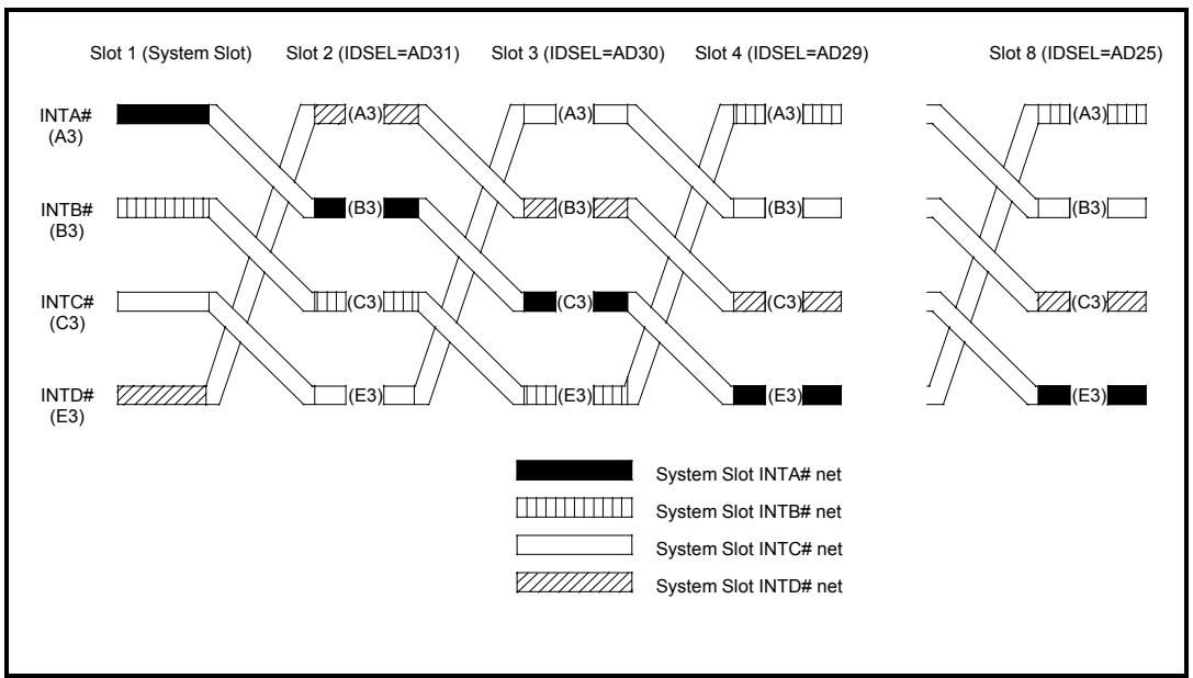
![This diagram illustrates signal routing across five columns labeled **Slot 1 (System Slot)**, **Slot 2 (IDSEL=AD31)**, **Slot 3 (IDSEL=AD30)**, **Slot 4 (IDSEL=AD29)**, and **Slot 8 (IDSEL=AD25)**. Four rows are labeled on the left: **INTA# (A3)**, **INTB# (B3)**, **INTC# (C3)**, and **INTD# (E3)**.  A legend at the bottom defines four network types by their fill style: *   **Black rectangle:** System Slot INTA# net *   **Vertical stripes rectangle:** System Slot INTB# net *   **White rectangle:** System Slot INTC# net *   **Diagonal hatched rectangle:** System Slot INTD# net  The diagram shows four continuous diagonal traces connecting blocks across the slots:  1.  **Trace starting at INTA# (A3):** Begins at Slot 1 with a black block. It connects to Slot 2, passing through a block labeled **(B3)** with a black fill. It continues to Slot 3, passing through a block labeled **(B3)** with diagonal hatching. It proceeds to Slot 4, passing through a block labeled **(B3)** with a white fill. Finally, it connects to Slot 8, passing through a block labeled **(B3)** with a white fill. 2.  **Trace starting at INTB# (B3):** Begins at Slot 1 with a vertical stripes block. It connects to Slot 2, passing through a block labeled **(A3)** with diagonal hatching. It continues to Slot 3, passing through a block labeled **(A3)** with a white fill. It proceeds to Slot 4, passing through a block labeled **(A3)** with diagonal hatching. Finally, it connects to Slot 8, passing through a block labeled **(A3)** with diagonal hatching. 3.  **Trace starting at INTC# (C3):** Begins at Slot 1 with a white block. It connects to Slot 2, passing through a block labeled **(C3)** with vertical stripes. It continues to Slot 3, passing through a block labeled **(C3)** with a black fill. It proceeds to Slot 4, passing through a block labeled **(C3)** with diagonal hatching. Finally, it connects to Slot 8, passing through a block labeled **(C3)** with diagonal hatching. 4.  **Trace starting at INTD# (E3):** Begins at Slot 1 with a diagonal hatched block. It connects to Slot 2, passing through a block labeled **(E3)** with a white fill. It continues to Slot 3, passing through a block labeled **(E3)** with vertical stripes. It proceeds to Slot 4, passing through a block labeled **(E3)** with a black fill. Finally, it connects to Slot 8, passing through a block labeled **(E3)** with a black fill.](.cpci-2-0-specification/7ebe5a50dcd6141eddf87b2275f1af093f1ca07bc3dfb7206d67739ba672d673.jpg)

# 3.2.7 CompactPCI Signal Additions

CompactPCI utilizes PCI signals as defined by the PCI Local Bus Specification with some additional signals. These additional signals do not affect the PCI signals but may enhance system operation by providing push button reset, power supply status, System Slot identification, geographic addressing, system management, and legacy IDE interrupt support features.

# 3.2.7.1 Push Button Reset (PRST#)

PRST# may be used in a CompactPCI system to reset the System Slot board, which in turn would reset the rest of the system using the PCI RST# signal. PRST# is an active low true TTL signal generated by a switch closure or an open-collector driver. It is the responsibility of the System Slot board receiving PRST# to debounce it as required. The System Slot board shall terminate PRST# with a minimum 1KΩ pullup resistor to V(I/O).

# 3.2.7.2 Power Supply Status (DEG#, FAL#)

Power sub-system status may be determined from two low true TTL power supply status signals available on backplanes utilizing modular power supplies implementing the optional DEG# and FAL# signals. The System Slot board shall terminate both signals with a minimum 1KΩ pullup resistor to V(I/O), even if the system board does not use these signals. Please see Section 3.2.8.2 for more information.

# 3.2.7.3 System Slot Identification (SYSEN#)

This pin is grounded on the CompactPCI backplane segment at the System Slot so the board may identify installation into the System Slot. This pin is not connected on the backplane for the remaining slots. Boards that sense this signal shall provide their own pull-up to V(I/O) and disable all System Slot functions, such as clock generation and bus arbitration when it is not installed in a System Slot.

# 3.2.7.4 Legacy IDE Interrupt Support

Two additional non-PCI interrupts, INTP and INTS, are defined for boards using legacy interrupts. Support of these interrupts is optional. INTP (pin D4) is used as a steerable interrupt which may be routed to any legacy ISA interrupt on the system master. The system master shall provide a way for the user to control the usage and routing of this interrupt, e.g. via the BIOS setup menu. After PCI Reset, this steerable interrupt shall be disabled on the system master and any peripheral board supporting this interrupt.

On legacy system masters, INTP may be hardwired to a single legacy ISA interrupt. This especially includes the option to use INTP as legacy IDE interrupt as proposed by former revisions of this specification.

INTP is an active high TTL signal and does not have the requirement of meeting the PCI electrical buffer characteristics. The System Slot board shall provide a 1KΩ pullup to V(I/O), even if the System Slot board does not support this signal.

INTS (pin E4) may be used as serialized interrupt in compliance with the ”Serialized IRQ Support for PCI Systems” specification, Rev. 6.0, September 1995.

The system master shall provide a way for the user to control the usage and routing of this interrupt, e.g. via the BIOS setup menu. After PCI Reset, this serialized interrupt shall be disabled on the system master and any peripheral boards supporting the serialized IRQ protocol.

INTS is synchronous to the PCI clock and has the requirement of meeting the PCI electrical buffer characteristics. This line shall have a pull up resistor on the system slot board in accordance with Section 3.1.8 and a termination resistor in accordance with Section 3.1.3 on any board supporting this signal. The electrical characteristics and routing of the PCB trace shall comply with sections 3.1.4 through 3.1.7.

The support for INTP and INTS shall be clearly documented by the system slot and peripheral board vendors.

# 3.2.7.5 System Enumeration (ENUM#)

This low true TTL open-collector signal shall be driven by hot swap compatible boards after insertion and prior to removal. The System Master uses this interrupt signal to force software to interrogate all boards within the system for resource allocation regarding I/O, memory, and interrupt usage. The System Slot board shall terminate ENUM# with a pullup resistor as defined in Section 3.1.8. Different levels of hot swap capability are defined in the CompactPCI Hot Swap Specification regarding the ENUM# Signal. Consult the CompactPCI Hot Swap Specification for further details.

# 3.2.7.6 Geographic Addressing (GA[4..0])

For backplanes, if P2 is populated on a particular slot, then it shall support the GA[4..0] geographic addressing signals for unique slot identification. Boards that use geographical address signals GA[4..0] shall be pulled up with a 10.0 KΩ ±10% resistor.

For backplanes the physical slot address (GA[4..0]) shall be encoded on the backplane by grounding and leaving unconnected different combinations of pins at each connector. Physical slot addresses are defined by the physical slot number in Section 2.1. Table 9 illustrates the physical slot number and its physical slot address defined by GA[4..0]. Physical slot “0” is reserved for future use. Geographical address “31” is the default address that results when a geographical address capable board is installed in a backplane slot that does not support geographical addressing.

Boards that support system management may use these signals to provide a unique address within the system. Refer to the pending CompactPCI System Management Specification for further information

Table 9. Physical Slot Addresses.

<table><tr><td>Physical Slot Number</td><td>GA[4](J2-A22)</td><td>GA[3](J2-B22)</td><td>GA[2](J2-C22)</td><td>GA[1](J2-D22)</td><td>GA[0](J2-E22)</td></tr><tr><td> $0^{(1)}$ </td><td>GND</td><td>GND</td><td>GND</td><td>GND</td><td>GND</td></tr><tr><td>1</td><td>GND</td><td>GND</td><td>GND</td><td>GND</td><td>Open</td></tr><tr><td>2</td><td>GND</td><td>GND</td><td>GND</td><td>Open</td><td>GND</td></tr><tr><td>3</td><td>GND</td><td>GND</td><td>GND</td><td>Open</td><td>Open</td></tr><tr><td>4</td><td>GND</td><td>GND</td><td>Open</td><td>GND</td><td>GND</td></tr><tr><td>5</td><td>GND</td><td>GND</td><td>Open</td><td>GND</td><td>Open</td></tr><tr><td>6</td><td>GND</td><td>GND</td><td>Open</td><td>Open</td><td>GND</td></tr><tr><td>7</td><td>GND</td><td>GND</td><td>Open</td><td>Open</td><td>Open</td></tr><tr><td>8</td><td>GND</td><td>Open</td><td>GND</td><td>GND</td><td>GND</td></tr><tr><td>9</td><td>GND</td><td>Open</td><td>GND</td><td>GND</td><td>Open</td></tr><tr><td>10</td><td>GND</td><td>Open</td><td>GND</td><td>Open</td><td>GND</td></tr><tr><td>11</td><td>GND</td><td>Open</td><td>GND</td><td>Open</td><td>Open</td></tr><tr><td>12</td><td>GND</td><td>Open</td><td>Open</td><td>GND</td><td>GND</td></tr><tr><td>13</td><td>GND</td><td>Open</td><td>Open</td><td>GND</td><td>Open</td></tr><tr><td>14</td><td>GND</td><td>Open</td><td>Open</td><td>Open</td><td>GND</td></tr><tr><td>15</td><td>GND</td><td>Open</td><td>Open</td><td>Open</td><td>Open</td></tr><tr><td>16</td><td>Open</td><td>GND</td><td>GND</td><td>GND</td><td>GND</td></tr><tr><td>17</td><td>Open</td><td>GND</td><td>GND</td><td>GND</td><td>Open</td></tr><tr><td>18</td><td>Open</td><td>GND</td><td>GND</td><td>Open</td><td>GND</td></tr><tr><td>19</td><td>Open</td><td>GND</td><td>GND</td><td>Open</td><td>Open</td></tr><tr><td>20</td><td>Open</td><td>GND</td><td>Open</td><td>GND</td><td>GND</td></tr><tr><td>21</td><td>Open</td><td>GND</td><td>Open</td><td>GND</td><td>Open</td></tr><tr><td>22</td><td>Open</td><td>GND</td><td>Open</td><td>Open</td><td>GND</td></tr><tr><td>23</td><td>Open</td><td>GND</td><td>Open</td><td>Open</td><td>Open</td></tr><tr><td>24</td><td>Open</td><td>Open</td><td>GND</td><td>GND</td><td>GND</td></tr><tr><td>25</td><td>Open</td><td>Open</td><td>GND</td><td>GND</td><td>Open</td></tr><tr><td>26</td><td>Open</td><td>Open</td><td>GND</td><td>Open</td><td>GND</td></tr><tr><td>27</td><td>Open</td><td>Open</td><td>GND</td><td>Open</td><td>Open</td></tr><tr><td>28</td><td>Open</td><td>Open</td><td>Open</td><td>GND</td><td>GND</td></tr><tr><td>29</td><td>Open</td><td>Open</td><td>Open</td><td>GND</td><td>Open</td></tr><tr><td>30</td><td>Open</td><td>Open</td><td>Open</td><td>Open</td><td>GND</td></tr><tr><td>31</td><td>Open</td><td>Open</td><td>Open</td><td>Open</td><td>Open</td></tr></table>

Note:

(1) Physical slot number “0” is reserved for future use.

# 3.2.7.7 System management bus

Three pins, (IPMB\_SCL, IPMB\_SDA, IPMB\_PWR), are defined on J1/P1 for incorporating system management features including board identification, environmental and voltage monitoring, etc.

Three pins, (ICMB\_SCL, ICMB\_SDA, ICMB\_PWR), are reserved on J2/P2 for possible use by non-backplane bussed system management functions.

Refer to the PICMG 2.9, CompactPCI System Management Specification for further information.

The IPMB\_PWR backplane traces shall have a current carrying capacity of at least 100 mA per slot.

# 3.2.8 Power Distribution

Power is distributed in a CompactPCI system by utilizing a backplane. Each backplane shall make provisions for the standard regulated direct current (DC) supply voltages in Table 10 below.

Table 10. Power Specifications.

<table><tr><td>Mnemonic</td><td>Description</td><td>Nominal Value</td><td>Tolerance(2)</td><td>Max. Ripple (p-p)(3)</td></tr><tr><td>5 V</td><td>+5 VDC</td><td>5.0 V</td><td>+5%/-3%</td><td> $50\mathrm {mV}^{(1)(4)}$ </td></tr><tr><td>3.3 V</td><td>+3.3 VDC</td><td>3.3 V</td><td>+5%/-3%</td><td> $50\mathrm {mV}^{(1)(4)}$ </td></tr><tr><td>+12 V</td><td>+12 VDC</td><td>12.0 V</td><td>±5%</td><td> $240\mathrm {mV}^{(1)(5)}$ </td></tr><tr><td>-12 V</td><td>-12 VDC</td><td>-12.0 V</td><td>±5%</td><td> $240\mathrm {mV}^{(1)(5)}$ </td></tr><tr><td>V(I/O)</td><td>PCI I/O Buffer Voltage</td><td>5.0V or 3.3V</td><td>+5%/-3%</td><td> $50\mathrm {mV}^{(1)(4)}$ </td></tr><tr><td>GND</td><td>Ground</td><td></td><td></td><td></td></tr></table>

# Note:

(1) Maximum ripple is very difficult to accurately measure and therefore requires good measurement techniques. Measurement should be made at 20 MHz bandwidth with a minimum length ground strap. Each CompactPCI slot must meet this specification.
(2) This specification is for power delivered to each slot and it includes both the power supply and the backplane tolerance.
(3) For ripple directly related to the line frequency, the maximum ripple shall be a maximum 10mV(p-p) for +12V and -12V and 5mV(p-p) for +5V and +3.3V

(4) Distribution between board and backplane: 20 mV for backplane; 30mV for board.
(5) Distribution between board and backplane: 96 mV for backplane; 144 mV for board.

# 3.2.8.1 External Power Connections

Power terminals may be located on the front or rear side of the backplane for external power sources. Several styles of high current printed circuit board terminals are available. At least one per supply voltage shall be provided.

# 3.2.8.2 In-Rack Power Connections

The PICMG 2.11 Power Interface Specification defines several methods for implementing In-rack modular power supplies. Previous versions of the core specification (PICMG 2.0) have referenced an IEC 603-2 (DIN 41612) style connector for modular power supplies, which is one of the referenced configurations in PICMG 2.11. For further details refer to PICMG 2.11 Power Interface Specification.

# 3.2.8.3 V(I/O) Current Carrying Capability

Backplanes shall be designed to provide an aggregate 4A minimum to each CompactPCI slot through that slot's V(I/O) pins. Boards may assume that up to 4A of current (at either 5V or 3.3V) is available through the V(I/O) pins at the connector. This requirement merely grants permission for boards to draw power from V(I/O) in addition to 5V and 3.3V power pins. Overall system power allocation is a system integration concern.

# 3.2.9 Power Decoupling

CompactPCI boards may utilize any of the voltages in Table 10. Without adequate power decoupling on the backplane for the 5 V and 3.3 V power, intermittent operation may result. The backplane has dedicated 5 V and 3.3 V power pins along with V(I/O) power pins. The V(I/O) power pins are connected to either 5 V or 3.3 V depending on if 5 V or 3.3 V backplane signals are being used. See Section 5.6.

All power voltages shall be decoupled to ground in such a manner as to provide for reasonable management of switching currents (di/dt). Low impedance power planes and connections to low equivalent series resistance (ESR) capacitors should be used. Even if a system does not use 3.3 or 5 V, the unused power pins shall be connected and decoupled to provide an additional AC return path.

Table 11 illustrates the bypass guidelines that shall, at a minimum, be used for each connector.

Table 11. Backplane Decoupling Recommendations.

<table><tr><td>Mnemonic</td><td>Description</td><td>Decoupling Capacitance</td><td>Voltage</td></tr><tr><td>5V</td><td>+5 VDC</td><td> $44 \mu F \pm 20\%^{(1)}$ </td><td>15 V min.</td></tr><tr><td>3.3V</td><td>+3.3 VDC</td><td> $44 \mu F \pm 20\%^{(1)}$ </td><td>10 V min.</td></tr><tr><td>V(I/O)</td><td>+5/3.3 VDC</td><td> $44 \mu F \pm 20\%^{(1)}$ </td><td>15 V min.</td></tr><tr><td>+12V</td><td>+12 VDC</td><td> $15 \mu F \pm 20\%$ </td><td>35 V min.</td></tr><tr><td>-12V</td><td>-12 VDC</td><td> $15 \mu F \pm 20\%$ </td><td>35 V min.</td></tr></table>

Note:
(1) Recommended decoupling capacitance per connector best distributed across the length of each connector.

# 3.2.10 Healthy (Healthy#)

This pin is reserved for use in hot swap systems. The backplane SHALL leave HEALTHY# open (not connected). This pin SHALL be bypassed on the backplane at each slot with a 0.01uF capacitor to maintain the AC shielding capability of the line. Additional requirements may apply to some Hot Swap platforms, refer to PICMG 2.1 for details.

# 3.3 33 MHz PCI Clock Distribution

The System Slot board shall provide clock signals for all PCI peripherals in the system, including devices on the System Slot board. Peripheral boards are provided clock signals via the CompactPCI backplane. A maximum skew of 2 ns shall be maintained across the system operating at 33 MHz between any two PCI devices at the clock input of the integrated circuits.

Clock skew is the difference between the maximum and minimum propagation delay of any PCI clock signal. There are two components that contribute to clock skew in a CompactPCI system:

1. Backplane Clock Skew. The CompactPCI backplane provides the distribution of clock signals for all of the board slots in the system. The differences in the trace routing and net topologies contribute to skew and also define the longest clock delay that shall be considered in the design of the system and still meet overall system clock skew requirements.
2. System Slot Board Clock Skew. This is the clock skew that may be attributed to the onboard routing differences (if any) of all of the PCI clocks as well as the skew specification for the type of integrated circuit driver used for clock distribu-

tion. The onboard clock routing shall be designed to complement the propagation delays of distributing the clock to a backplane and still meet overall system skew requirements.

# 3.3.1 Backplane Clock Routing Design Rules

CompactPCI backplanes shall be designed to provide a consistent environment for System Slot boards with regard to backplane clock routing. Design rules assume a linear backplane with the System Slot at one end of the bus segment and 20.32 mm (0.8 inch) connector spacing.

The System Slot provides 7 clock signals, which dedicates a unique clock to each slot. Correspondence between individual clock signals and physical slots is arbitrary.

Backplanes shall use these clock lines to provide a single clock line per slot. Clock lines shall not be shared. These clock lines shall be routed between 135 mm (5.3 inches) and 185 mm (7.3 inches) in length.

System Slot boards shall drive each of the 7 clock lines.

# 3.3.2 System Slot Board Clock Routing Design Rules

The System Slot clock distribution circuitry shall be designed to accommodate up to 1.2 ns of backplane skew (minimum vs. maximum number of slots and various loading configurations). The following design rules apply to clock distribution to backplane peripherals and local (onboard) PCI peripherals. See Section 3.1.3 for details of termination on System Slot Boards.

# 3.3.2.1 Clock Routing to Connector Clock Pins

The clock distribution circuitry on the System Slot shall provide a discrete clock signal to each of the CompactPCI connector pins defined as a PCI clock (CLK0, CLK1, CLK2, CLK3, CLK4, CLK5, CLK6). The routing of these signals shall be matched in length.

# 3.3.2.2 Clock Routing to Local PCI Peripherals

Any onboard PCI peripherals connected to the CompactPCI bus, including PCI to PCI bridges, shall be provided a clock that is delayed to accommodate the maximum propagation delay of the backplane clocks and still meet the 2 ns overall skew requirement of the PCI Specification. Up to 800 ps of skew is allowed for onboard clock distribution (including the clock buffer internal skew). The onboard clock signals shall be delayed beyond the clocks routed to the backplane (Section 3.3.2.1) to accommodate best and worst case backplane delays and the 63.5mm wire delay on the peripheral board.

# 3.4 64-Bit Design Rules

64-bit Peripheral boards must be configured correctly for the type of backplane environment that they are plugged into. This includes 64-bit Peripheral boards plugged into a system controlled by a 32-bit System Master as well as a 64-bit Peripheral board being plugged into a hot swap capable system. This revision of the CompactPCI specification differs from the PCI specification in the method that a Peripheral board determines the proper mode of operation.

The PCI Specification requires the following: On a 64-bit Peripheral board (32-bit Peripheral boards ignore REQ64#) REQ64# is sampled by the peripheral PCI device at the rising (trailing) edge of RST# to configure the upper 32-bit signal buffers for the type of system that the peripheral is installed into. If REQ64# is high, the 64-bit device is allowed to drive the upper 32-bits signals active to prevent these signals from floating. If REQ64# is sampled low, the device must configure the upper 32- bit signals for proper 64-bit operation.

CASE A: In CompactPCI, it is possible to have a 64-bit System Slot board plugged into a 32-bit only backplane, in which case it is required that any 64-bit Peripheral boards terminate the upper 32-bit signals for non 64-bit operation.

CASE B: It is also desirable to allow 64-bit Peripheral boards to communicate with each other at 64-bits when in a 64-bit backplane controlled by a 32-bit System Slot board. It is also desirable to allow the backplane to contain a mix of 32-bit and 64-bit slots.

CASE C: In a hot swap system, a board must configure itself because the time for a system reset has long passed and the board is being installed in an operating backplane environment with PCI transactions occurring.

To allow boards to self configure for 64-bit operation, pin B5 of P2 is defined as 64EN# and is GROUND in 64-bit backplanes and is left unconnected in 32-bit backplanes. This signal is then used by onboard circuitry to self-configure during RST#.

64EN# may be used in different ways to configure the local device. These include, but are not limited to, the following implementations:

a) Using 64EN# to drive the devices REQ64# signal during local reset by decoupling the backplane REQ64# from the device during reset. After reset, the backplane REQ64# is then connected to the device for normal 64-bit handshake operation. In all cases, normal electrical operation of REQ64# shall be maintained after reset. See Figure 4 below for an example of a possible circuit topology.
b) A 64-bit device may directly sample 64EN# during local reset to configure for 32- or 64-bit operation.

c) 64EN# may be used as part of an EEPROM serial pre-load mechanism to configure a 64-bit device for proper operation.

64-bit Peripheral boards shall use 64EN# to self-configure. Using the state of REQ64# at the trailing edge of RST# is no longer allowed. With the requirements given in this revision of the CompactPCI Specification, 64-bit capability is no longer an overall platform attribute. 64-bit capability can be determined on a slot by slot basis.

The following circuit topology shows a FET in series with the backplane REQ64# and the devices REQ64# pin. During reset, the FET is OFF, and the resistance to the 64EN# pin configures the device at the rising edge of reset. When RST# is deasserted, the FET is enabled and REQ64# is allowed to function in it’s normal mode (As defined in PCI Specification 2.1).

![Based on the provided image, here is the accurate description of the flowchart/circuit diagram:  **Labeled Blocks and Components:** *   **VIO** (Top signal rail) *   **1KΩ** (Resistor) *   **64EN#** (Input block) *   **50KΩ** (Resistor) *   **REQ64#** (Input block) *   **FET** (Transistor block) *   **LOCAL RST#** (Signal line) *   **PCI DEVICE** (Large output block containing input pins labeled **REQ64#** and **RST#**)  **Connections:** *   **VIO** connects to the top of the **1KΩ** resistor. *   The bottom of the **1KΩ** resistor connects to a junction point. *   The right side of the **64EN#** block connects to this same junction point. *   The top of the **50KΩ** resistor connects to this same junction point. *   The bottom of the **50KΩ** resistor connects to a second junction point. *   The right side of the **FET** block connects to this second junction point. *   This second junction point connects to the **REQ64#** input pin of the **PCI DEVICE**. *   The left side of the **REQ64#** block connects to the left side of the **FET** block. *   The **LOCAL RST#** line connects to the bottom of the **FET** block. *   The **LOCAL RST#** line connects to the **RST#** input pin of the **PCI DEVICE**.](.cpci-2-0-specification/d5366dbcf095eeab07a4120ae04e46145dc2ea414ff424a7eeff94501834aabe.jpg)

Figure 4. Local 64 Bit Initialization

To allow for the addition of the REQ64# series FET, the FET must not exceed the following parameters:

ON resistance: 5-10Ω typical

The capacitance of the FET circuit must be isolated from ground. One method of accomplishing isolation of the FET capacitance is to use a discrete 3-Terminal FET, with the device's gate driven through a high valued resistor.

The FET may replace the 10Ω CompactPCI  stub isolation resistor, but the circuit topology must provide the equivalent stub isolation of a non-FET implementation. Refer to the CompactPCI Hot Swap Specification (PCIMG 2.1 R1.0) for details of the hot swap circuit analysis.

# 3.5 66 MHz Electrical Requirements

This section documents the additional requirements for 66 MHz operation. 33 MHz design rules apply for features not specifically called out in this section.

# 3.5.1 66 MHz Board Design Rules

On 66 MHz Peripheral boards, the PCI clock signal length shall be 63.5 mm ±1 mm (2.5 inches ±0.04 inches), and shall drive only one load on the board. Inner layer stripline construction shall be used for all clock lines in order to equalize delays.

# 3.5.2 66 MHz System Board Design Rules

On 66MHz System Slot Boards only one PCI load shall be allowed.

# 3.5.3 66MHz Backplane Design Rules

66 MHz CompactPCI defines a backplane environment that may have up to five slots.

One slot, the System Slot, provides the clocking, arbitration, configuration, and interrupt processing for the other four slots. Fewer slots may be provided in a CompactPCI backplane, but the following sections assume that a maximum configuration is employed in a linear topology using 20.32 mm (0.8 inch) board center-to-center spacing with the System Slot located on either end of the bus segment. Any other topology shall be simulated or otherwise verified to ensure compliance to the PCI specification.

M66EN, the 66Mhz Enabling Line, shall be bussed to all slots in 66Mhz backplanes.

Backplanes shall provide separate power planes for 3.3 V, 5 V, and ground. V(I/O) shall always be configured as 3.3V.

# 3.5.4 66MHz PCI Clock Distribution

The System Slot board shall provide clock signals for all PCI peripherals in the system, including the device on the System Slot board. Peripheral boards are provided clock signals via the CompactPCI backplane. A maximum skew of 1 ns shall be maintained across the system operating at 66 MHz between any two PCI devices at the clock input of the integrated circuits.

Clock skew is the difference between the maximum and minimum propagation delay of any PCI clock signal. There are two components that contribute to clock skew in a CompactPCI system:

1. Backplane Clock Skew. The CompactPCI backplane provides the distribution of clock signals for all of the board slots in the system. The slight differences in the

CompactPCI® Core Specification PICMG 2.0 D3.0 9/24/99

Draft for PICMG Executive Ballot

Do not specify or claim conformance to this specification - Not for Distribution trace routing and net topologies contribute to skew and also define the longest clock delay that shall be considered in the design of the system and still meet overall system clock skew requirements.

2. System Slot Board Clock Skew. This is the clock skew that may be attributed to the onboard routing differences (if any) of all of the PCI clocks as well as the skew specification for the type of integrated circuit driver used for clock distribution. The onboard clock routing shall be designed to complement the propagation delays of distributing the clock to a backplane and still meet overall system skew requirements. A System Slot board designed for both 33 MHz and 66 MHz operation shall be designed with consideration for the different clock environments that it may operate in.

# 3.5.4.1 66 MHz backplane clock routing design rules

66 MHz systems require only 4 Peripheral Slot clocks to be connected. Correspondence between individual clock signals and physical slots is arbitrary.

Backplanes shall use these clock lines to provide a single clock line per slot. Clock lines shall not be shared. These clock lines shall be routed to 160mm ±1mm (6.300 inches ± 0.04) in length.

Inner layer stripline construction shall be used for all clock lines in order to equalize delays. Vias shall not be used to route any backplane clock lines.

# 3.5.5 66 MHz System Slot Board Clock Routing Design Rules

The System Slot clock distribution circuitry shall be designed to accommodate up to 200 ps of backplane and peripheral board skew. The following design rules apply to clock distribution to backplane peripherals and local (onboard) PCI peripherals.

# 3.5.5.1 Clock Routing to Connector Clock Pins

The clock distribution circuitry on the System Slot shall provide a discrete clock signal to each of the CompactPCI connector pins defined as a PCI clock (CLK0, CLK1, CLK2, CLK3, CLK4, CLK5, and CLK6). The routing of these signals shall be matched in length.

# 3.5.5.2 Clock Routing to Local PCI Peripherals

Any onboard PCI peripherals connected to the CompactPCI bus, including PCI to PCI bridges, shall be provided a clock that is delayed to accommodate the maximum propagation delay of the backplane clocks and still meet the 1 ns overall skew requirement. Up to 800 ps of skew is allowed for onboard clock distribution (including the clock buffer internal skew). The onboard clock signals shall be delayed beyond the clocks routed to the backplane (Section 3.5.5.1) to accommodate best and worst case backplane delays and the 63.5mm wire delay on the peripheral board.

# 3.5.6 66 MHz Hot Swap

66MHz host silicon is not typically designed to dynamically switch between 33MHz and 66MHz operation. Because of this, hot swapping 33MHz peripherals into an operating 66MHz backplane is not allowed, unless the host silicon supports dynamic frequency change.

Removing a 33MHz peripheral from, what would otherwise be, a 66MHz platform is also not allowed, unless the host silicon continues to operate at 33MHz, or the host silicon supports dynamic frequency change.

# 3.6 System and Board Grounding

# 3.6.1 Board Front Panel Grounding Requirements

CompactPCI boards should utilize metalized shell front panel connectors for EMI/RFI protection. The shell should be electrically connected to the front panel through a low impedance path.

The following practice is prescribed for CompactPCI:

a) The front panel shall be connected to frame ground and isolated from logic ground.
b) CompactPCI boards should provide a mechanism to connect frame ground (on front panel) through a low impedance path to logic ground used on board. This will allow for flexibility in system integration for applications with differing grounding practices.

# 3.6.2 Backplane Grounding Requirements

Backplanes shall provide isolation between frame ground and logic ground. CompactPCI Backplanes should provide a configurable method of connecting frame ground to logic ground on the backplane. The intent of this is to allow the systems integrator the option to configure the grounding scheme as needed.

# 3.7 CompactPCI Buffer Models

The CompactPCI simulation V-I curve assumptions are provided in Appendix A for reference. Both 5V and 3.3V buffer models are provided. Note that all 66 MHz simulation assumes 3.3V buffers only. 33 MHz environments have been simulated with 5V, 3.3V and Universal buffer models.

This page is left intentionally blank

# 4 Mechanical Requirements

# 4.1 Board Requirements

CompactPCI defines two board sizes, 3U and 6U.

# 4.1.1 3U Boards

3U boards are 100 mm by 160 mm. The PCB is 1.6 ±0.2 mm thick. A 2 mm (IEC-61076-4-101) connector is used for interfacing to the CompactPCI bus segment. Figure 6 illustrates the 3U board dimensions and connector location. 32-bit PCI is implemented on J1. J2 may be used for 64-bit PCI signaling, rear-panel I/O, or System Slot functions.

Note that row Z is not present on connectors J1 and J2 used on system or peripheral boards. Refer to IEC-61076-4-101 documentation for details.

# 4.1.2 6U Boards

6U boards are 233.35 mm by 160 mm. Figure 7 illustrates the 6U board dimensions and connector locations J1, J2, J3, J4 and J5. 32-bit PCI is implemented on J1. J2 is used for 64-bit PCI signaling, rear-panel I/O, or System Slot functions. J3, J4 and J5 may be used for rear-panel I/O.

Rear-panel I/O may be defined by the user and/or utilize PICMG specifications. Contact PICMG for copies of these specifications.

Note that row Z is not present on connectors J1 and J2 used on system or peripheral boards. Refer to IEC-61076-4-101 documentation for details.

# 4.1.3 Rear-panel I/O Boards

Rear-panel I/O boards may be either 3U (100 mm) or 6U (233.35 mm) in height and shall be 80 mm in depth for standard applications.

Figure 9 and Figure 10 illustrate 3U and 6U respectively, 80 mm representative rear-panel I/O board defined by IEEE 1101.11. Other depths as defined by IEEE 1101.11 are allowed depending on the application requirements. Refer to IEEE 1101.11 for further details. Since rear panel I/O is not available on J1, and therefore rear panel I/O necessitates additional connectors, these implementations shall be keyed to conform to the PICMG 2.10, Keying of CompactPCI Boards and Backplanes specification. The keying combination used on the rear panel I/O module shall match that used on the corresponding front panel.

# 4.1.4 ESD Discharge Strip

All boards shall implement features for ESD protection defined by IEEE 1101.10 and IEEE1101.11. The minimum ESD requirement for a board shall be a discharge strip located along both sides of the bottom edge of the board.

Figure 8 and Figure 11 shows the implementation for a front plug-in board and a rear panel I/O board respectively.

When a board is inserted into an enclosure, the ESD strip connects with an ESD clip on the cardguide which is connected to chassis ground, see 4.1.5. The ESD strip is separated into three segments to achieve a “controlled discharge”. The first segment is connected to the front panel through a 10MΩ=resistance to discharge any built up static from the board or user. The resistor is used to limit the amount of discharge current. The second segment discharges the board’s ground planes as it is inserted further into the cardguide; again through a 10 MΩ=resistance. The final third segment has a direct connection to the front panel. This provides a discharge path as the backplane connectors engage and when the board comes to rest after being completely installed. The third segment also provides a discharge path from the front panel to chassis ground when the entire system is assembled making it safe for handling and operation.

The level of ESD protection required depends upon the environment. For example, humans in dry ambient conditions can generate ESD potentials of over 20 kV. Use of an ESD wrist strap connected to chassis ground will limit the maximum potential to well below 2.5 kV. Other standard ESD reduction techniques such as natural-fiber wool apparel for service uniforms, minimum 35% RH operating environments, conductive mats or flooring, etc, are also helpful. For the discharge circuitry to be effective, no arc-over must occur across the resistor nor to surrounding components or circuitry. This implies (1) the breakover potential of the 10 MΩ=discharge resistance must exceed the expected ESD potential buildup, and (2) the clearance area between the discharge circuitry and surrounding components or circuitry must be adequate to prevent arc-over. Discharge resistors that can tolerate high voltage levels are physically large. Fortunately, the breakdown voltage of resistors in series is additive and stray capacitance is sufficient to equalize the potential across each resistor. So if N resistors is used in series, of 10MΩ/NΩ=resistance, the total breakdown voltage to N times the single resistor value.

# 4.1.5 ESD Clip

The ESD cardguide clip contacts the board edge as the board is inserted in the system and provides a path for ESD energy on the board to be discharged into the chassis. An ESD clip shall be provided in the lower card guide. The location of this clip shall be 35mm ± 5mm (1.38 inches ± 0.2 inches)

from the front attachment plane as shown in Figure 5. Note, this dimension is tighter than the location defined in IEEE 1101.10. These dimensions shall apply to both front and rear card guides.

![Attachment Plane Far Edge of Clip 35mm ± 5mm ≥ 10.0mm ESD CLIP Chassis](.cpci-2-0-specification/54a52ebf3539a1aaf457958013bfb4cf20cb17efd79f43cf6ffaa68253f98fa7.jpg)

Figure 5. ESD Clip Location

# 4.1.6 Cross Sectional View

Figure 12 provides a cross sectional view illustrating the relationship between the front panel, board, connectors, and backplane. Refer to IEEE 1101.1 and IEEE 1101.10 (EMC) for additional details. Note that the top connector shield (component side) shall be installed to meet the electrical requirements. The bottom connector shield (back side) may be installed if it does not protrude into the interboard separation plane.

# 4.1.7 Component Outline and Warpage

Component outline and warpage is shown Figure 13. The sum of the component height/lead lengths and warpage (bow and twist) shall remain within the boundaries specified by the interboard separation planes. See IEEE1101.1 and IEEE 1101.10 for additional details.

# 4.1.8 Solder Side Cover

A protective solder side cover may be required to prevent damage of backside components when boards are installed/extracted from the subrack. All boards having backside components or through-hole pins should provide a means for mounting a protective cover. All such boards should be equipped with a solder side cover. The mounting holes for an IEEE 1101.10 compliant protective cover should be used, see Figure 6, Figure 7,

Figure 9 and Figure 10.

![  Component                Dimension           ----------------------   ---------------     Component Keep-out Area   2.7 ± 0.1 4PL       Connector Positions      66.45 ± 0.3         Connector Positions      88.9 ± 0.1          Connector Positions      156.5               Connector Positions      152.93              Connector Positions      2PL                 Connector Positions      2.5                 Connector Positions      2PL                 Connector Positions      68.0                Connector Positions      2PL                 J1 Connector             2.0 ± 0.05/-0.00 (non-plated)     CompactPCI CONNECTOR   45° X 45'            J2 Connector             2mm X 45'            J1 Connector             2PL                 J1 Connector             16.43 ± 0.2: PCB Thickness     J1 Connector             3.5                 J1 Connector             2PL                 J1 Connector             2PL                 J1 Connector             2PL                 J1 Connector             2PL                 J1 Connector             2PL                 J1 Connector             2PL                 J1 Connector             2PL                 J1 Connector             2PL                 J1 Connector             2PL                 J1 Connector             2PL (Optional Mounting Holes Solder Side Cover or Tooling (2PL))     J1 Connector             2PL (Optional Mounting Holes Solder Side Cover or Tooling (2PL))     J1 Connector             2PL (Optional Mounting Holes Solder Side Cover or Tooling (2PL))     J1 Connector             2PL (Optional Mounting Holes Solder Side Cover or Tooling (2PL))     J1 Connector             2PL (Optional Mounting Holes SolderSide Cover or Tooling (2PL))     J1 Connector             2PL (Optional Mounting Holes Solder Side Cover or Tooling (2PL))     J1 Connector             2PL (Optional Mounting Holes Solder Side Cover or Tooling (2PL))     J1 Connector             2PL (Optional Mounting Holes Solder Side Cover or Tooling (2PL))     J1 Connector             2PL(Optional Mounting Holes Solder Side Cover or Tooling (2PL))     J1 Connector             2PL(Optional Mounting Holes Solder Side Cover or Tooling (2PL))     J1 Connector             2PL(Optional Mounting Holes Solder Side Cover or Tooling (2PL))     J1 Connector             2PL(Optional Mounting Holes Solder Side Cover or Tooling (2PL))     Joint Component           0.0/-0.3             Joint Component           -0.3                Joint Component           -0.3                Joint Component           -0.3                Joint Component           -0.3                Joint Component           -0.3                Joint Component           -0.3                Joint Component           -0.3                Joint Component           -0.3                Joint Component           -0.3                Joint Component           -0.3             ](.cpci-2-0-specification/37e65fed91fa0525405ebfb2337bc1e39b9c75dd4d64e9324489722deed95f63.jpg)

Figure 6. 3U Board.

![  Component             Dimension            --------------------- -------------------    Component Keep-out Area - Both Sides   8.00 ± 0.3            Component Keep-out area - Both Sides   2.5 ± 0.1             Component Keep-out area - Both Sides   201.35 ± 0.1          Component Keep-out area - Both Sides   199.80 ± 0.2          Component Keep-out area - Both Sides   205.35 ± 0.1          Component Keep-out area - Both Sides   233.35 ± 0.3          Component Keep-out area - Both Sides   66.45 ± 0.1           Component Keep-out area - Both Sides   88.9 ± 0.1           Component Keep-out area - Both Sides   22.45 ± 0.1           Component Keep-out area - Both Sides   28.0 ± 0.1           Component Keep-out area - Both Sides   156.5 ± 0.1           Component Keep-out area - Both Sides   152.93 ± 0.1          Component Keep-out area - Both Sides   6PL ± 0.1             Component Keep-out area - Both Sides   16.43 ± 0.1           Component Keep-out area - Both Sides   2PL ± 0.1             Component Keep-out area - Both Sides   2.5 ± 0.1             Component Keep-out area - Both Sides   2 PL ± 0.1             Component Keep-out area - Both Sides   8.00 ± 0.3            Component Keep-out area - Both Sides   160.0 ± 0.3          Component Keep-out area - Both Sides   205.35 ± 0.3          Component Keep-out area - Both Sides   201.35 ± 0.3          Component Keep-out area - Both Sides   205.35 ± 0.3          Component Keep-out area - Both Sides   201.35 ± 0.3          Component Keep-out area - Both Sides   205.35 ± 0.3          Component Keep-out area - Both Sides   201.35 ± 0, 2 PL         Component Keep-out area - Both Sides   205.35 ± 0, 2 PL         Component Keep-out area - Both Sides   201.35 ± 0, 2 PL         Component Keep-out area - Both Sides   205.35 ± 0, 2 PL         Component Keep-out area - Both Sides   201.35 ± 0, 2 PL         Component Keep-out area - Both Sides   205.35 ± 0              Component Keep-out area - Both Sides   201.35 ± 0, 2 PL         Component Keep-out area - Both Sides   205.35 ± 0, 2 PL         Component Keep-out area - Both Sides   201.35 ± 0, 2 PL         Component Keep-out area - Both Sides   205.35 ± 0            Component Keep-out area - Both Sides   201.35 ± 0, 2 PL         Component Keep-out area - Both Sides   205.35 ± 0            Component Keep-out area - Both Sides   201.35 ± 0, 2 PL         Component Keep-out area - Both Sides   205.35 ± 0            Component Fill Section     Reference/Note Change     J5 Connector Positions     1-22                  J4 Connector Positions     1-25                  J3 Connector Positions     1-19                  J2 Connector Positions     1-22                  J1 Connector Positions     1-25                  IEC-61076-4-10I PCB HOLE LAYOUT PCB HOLE LAYOUT 2mm SQUARE GRID      106.68                IEC-61076-4-10I PCB HOLE LAYOUT PCB HOLE LAYOUT 2mm SQUARE GRID      68.0                  IEC-61076-4-10I PCB HOLE LAYOUT PCB HOLE LAYOUT 2mm SQUARE GRID      70.68                 IEC-61076-4-10I PCB HOLE LAYOUT PCB HOLE LAYOUT 2mm SQUARE GRID      68.0                  IEC-61076-4-10I PCB HOLE LAYOUT PCB HOLE LAYOUT 2mm SQUARE GRID      70.68                 IEC-61076-4-10I PCB HOLE LAYOUT PCB HOLE LAYOUT 2mm SQUARE GRID      68.0                  IEC-61076-4-10I PCB HOLE LAYOUT PCB HOLE LAYOUT 2mm SQUARE GRID      70.68                 IEC-61076-4-10I PCB HOLE LAYOUT PCB HOLE LAYOUT 2mm SQUARE GRID      68.0                  IEC-61076-4-10I PCB HOLE LAYOUT PCB HOLE LAYOUT 2mm-square GRID      —                     IEC-61076-4-10I PCB HOLE LAYOUT PCB HOLE LAYOUT 2mm-square GRID      —                     IEC-61076-4-10I PCB HOLE LAYOUT PCB HOLE LAYOUT 2mm-square GRID      —                     IEC-61076-4-10I PCB HOLE LAYOUT DCB HOLE LAYOUT PCB HOLE LAYOUT 2mm-square GRID      —                     IEC-61076-4-10I PCB HOLE LAYOUT PCB HOLE LAYOUT 2mm-square GRID      —                     IEC-61076-4-10I PCB HOLE LAYOUT PCB HOLE LAYOUT 2mm-square GRID      —                     J1 Connector Positions     1-25                  J2 Connector Positions     1-22                  J3 Connector Positions     1-19                  J4 Connector Positions     1-25                  J5 Connector Positions     —                     J6 Connector Positions     —                     J7 Connector Positions     —                     J8 Connector Positions     —                     J9 Connector Positions     —                     J10 Connector Positions     —                     J11 Connector Positions     —                     J12 Connector Positions     —                     J13 Connector Positions     —                     J14 Connector Positions     —                     J15 Connector Positions     —                     J16 Connector Positions     —                     J17 Connector Positions     —                     J18 Connector Positions     —                     J19 Connector Positions     —                     J20 Connector Positions     —                     J21 Connector Positions     —                     J22 Connector Positions     —                     J23 Connector Positions     —                     J24 Connector Positions     —                     J25 Connector Positions     —                     J26 Connector Positions     —                     J27 Connector Positions     —                     J28 Connector Positions     —                     J29 Connector Positions     —                     J30 Connector Positions     —                     J31 Connector Positions     —                     J32 Connector Positions     —                     J33 Connector Positions     —                     J34 Connector Positions     —                     J35 Connector Positions     —                     J36 Connector Positions     —                     J37 Connector Positions     —                     J38 Connector Positions     —                     J39 Connector Positions     —                     J40 Connector Positions     —                     J41 Connector Positions     —                     J42 Connector Positions     —                     J43 Connector Positions     —                     J44 Connector Positions     —                     J45 Connector Positions     —                     J46 Connector Positions     —                     J47 Connector Positions     —                     J48 Connector Positions     —                     J49 Connector Positions     —                     J50 Connector Positions     —                     J51 Connector Positions     —                     J52 Connector Positions     —                     J53 Connector Positions     —                     J54 Connector Positions     —                     J55 Connector Positions     —                     J56 Connector Positions     —                     J57 Connector Positions     —                     J58 Connector Positions     —                     J59 Connector Positions     —                     J60 Connector Positions     —                     J61 Connector Positions     —                     J62 Connector Positions     —                     J63 Connector Positions     —                     J64 Connector Positions     —                     J65 Connector Positions     —                     J66 Connector Positions     —                     J67 Connector Positions     —                     J68 Connector Positions     —                     J69 Connector Positions     —                     J70 Connector Positions     —                     J71 Connector Positions     —                     J72 Connector Positions     —                     J73 Connector Positions     —                     J74 Connector Positions     —                     J75 Connector Positions     —                     J76 Connector Positions     —                     J77 Connector Positions     —                     J78 Connector Positions     —                     J79 Connector Positions     —                     J80 Connector Positions     —                     J81 Connector Positions     —                     J82 Connector Positions     —                     J83 Connector Positions     —                     J84 Connector Positions     —                     J85 Connector Positions     —                     J86 Connector Positions     —                     J87 Connector Positions     —                     J88 Connector Positions     —                     J89 Connector Positions     —                     J90 Connector Positions     —                     J91 Connector Positions     —                     J92 Connector Positions     —                     J93 Connector Positions     —                     J94 Connector Positions     —                     J95 Connector Positions     —                     J96 Connector Positions     —                     J97 Connector Positions     —                     J98 Connector Positions     —                     J99 Connector Positions     —                     A Detail A                 note: Notes: Refer to ESD Strip Detail  CompactPEI ALL DIMENSIONS IN MILLIMETERS TOLERES X.X= ± 0.1 TITLE:  6U MECHANICAL BOARD DIMENSIONS  DRAWN      DATE       NONE      DRAWING NO. PROD          DATE: 04/08/99](.cpci-2-0-specification/a147af804688bf07317b54436e1ebca69a6754b5a44558714c97ae3dd4d82578.jpg)

Figure 7. 6U Board.

![  Component           Value     -----------------   -----     Strip 1             10 MOhm     Strip 2             10 MOhm     Strip 3             10 MOhm     Strip 4             10 MOhm     Strip 5             10 MOhm     Strip 6             10 MOhm     Strip 7             10 MOhm     Strip 8             10 MOhm     Strip 9             10 MOhm     Strip 10            10 MOhm     Strip 11            10 MOhm     Strip 12            10 MOhm     Strip 13            10 MOhm     Strip 14            10 MOhm     Strip 15            10 MOhm     Strip 16            10 MOhm     Strip 17            10 MOhm     Strip 18            10 MOhm     Strip 19            10 MOhm     Strip 20            10 MOhm     Strip 21            10 MOhm     Strip 22            10 MOhm     Strip 23            10 MOhm     Strip 24            10 MOhm     Strip 25            10 MOhm     Strip 26            10 MOhm     Strip 27            10 MOhm     Strip 28            10 MOhm     Strip 29            10 MOhm     Strip 30            10 MOhm     Strip 31            10 MOhm     Strip 32            10 MOhm     Strip 33            10 MOhm     Strip 34            10 MOhm     Strip 35            10 MOhm     Strip 36            10 MOhm     Strip 37            10 MOhm     Strip 38            10 MOhm     Strip 39            10 MOhm     Strip 40            10 MOhm     Strip 41            10 MOhm     Strip 42            10 MOhm     Strip 43            10 MOhm     Strip 44            10 MOhm     Strip 45            10 MOhm     Strip 46            10 MOhm     Strip 47            10 MOhm     Strip 48            10 MOhm     Strip 49            10 MOhm     Strip 50            10 MOhm     Strip 51            10 MOhm     Strip 52            10 MOhm     Strip 53            10 MOhm     Strip 54            10 MOhm     Strip 55            10 MOhm     Strip 56            10 MOhm     Strip 57            10 MOhm     Strip 58            10 MOhm     Strip 59            10 MOhm     Strip 60            10 MOhm     Strip 61            10 MOhm     Strip 62            10 MOhm     Strip 63            10 MOhm     Strip 64            10 MOhm     Strip 65            10 MOhm     Strip 66            10 MOhm     Strip 67            10 MOhm     Strip 68            10 MOhm     Strip 69            10 MOhm     Strip 70            10 MOhm     Strip 71            10 MOhm     Strip 72            10 MOhm     Strip 73            10 MOhm     Strip 74            10 MOhm     Strip 75            10 MOhm     Strip 76            10 MOhm     Strip 77            10 MOhm     Strip 78            10 MOhm     Strip 79            10 MOhm     Strip 80            10 MOhm     Strip 81            10 MOhm     Strip 82            10 MOhm     Strip 83            10 MOhm     Strip 84            10 MOhm     Strip 85            10 MOhm     Strip 86            10 MOhm     Strip 87            10 MOhm     Strip 88            10 MOhm     Strip 89            10 MOhm     Strip 90            10 MOhm     Strip 91            10 MOhm     Strip 92            10 MOhm     Strip 93            10 MOhm     Strip 94            10 MOhm     Strip 95            10 MOhm     Strip 96            10 MOhm     Strip 97            10 MOhm     Strip 98            10 MOhm     Strip 99            10 MOhm     Strip A             DETAIL A    A ITEMS: • ESD STRIP LOCATIONS ARE TO BE PROVIDED • AT BOTH PRIMARY AND SECONDARY SIDES OF PCB • THIS DRAWING APPLIES TO THE BOOTTOM OF \( \mathbf{{3U}} \) • AND \( \mathbf{{6U}} \) BOARDS  PCI Industrial Computer Manufacturers Group (PICMG), 301 Edgewater Place, Suite \( \mathbf{{220}} \), Wakefield, MA \( \mathbf{{01880}}\mathbf{{USA}} \), Tel: \( \mathbf{{78I.224.1100}} \), Fax: \( \mathbf{{78I.224.1239}} \), www.picmg.org ALL DIMENSIONS ARE IN MILLIMETERS TOLERANCES: \( {0.x} \pm {0.2} \) \( {0.xx} \pm {0.05} \) TITLE: COMPACTPCI ESD STRIP DETAIL](.cpci-2-0-specification/b2728b95cd111fd58bde3c6a886c0db489a7e9cfb5948a526577f956f91532c5.jpg)

Figure 8. Front Side Board ESD Dimensions

![  Component   Dimension (mm)     :---   :---     Component Keep-out area - Both Sides   80.0 ± 0.0/-0.3     2mm X 45' 2 PL   2.5     68.0   Ø 2.7 ± 0.1 4PL     66.45 2PL   72.0     IEC-61076-4-101 PCB HOLE LAYOUT 2mm SQUARE GRID   2.5     CompactPCI CONNECTOR   2.0 +0.05/-0.00 (non-plated) 2PL     ∅ 2.0 +0.05/-0.00 (non-plated) 2PL   2.5     DETAIL A   24.0     3.5   16.43 2PL     72.50 2PL   76.50     RJ1 Connector Positions 1-25   28.0     RJ2 Connector Positions 1-22   100.0 +0.0/-0.3     Optional Mounting Holes Solder Side Cover or Tooling (2PL)   16.43 2PL     DetAIL A   3.5     DETAIL A   72.50 2PL     DetAIL A   76.50     DetAIL A   1.6 ±0.2 PCB Thickness   Note: Refer to ESD Strip Detail Notes: 1. Refer to ESD Strip Detail CompactPCI ALL DIMENSIONS IN MILLIMETERS SLOWSX.X ± 0.1 TITLE 3U REAR PANEL I/O BOARD DIMENSIONS REV DATE NC DRAWING NO ISSN DED DATE 06/01/99](.cpci-2-0-specification/6ea61a2db2f0530107b009967a2ee90f68e92140f0b8d551fea4b28cebed98f7.jpg)

Figure 9. 3U Rear-Panel I/O Board Dimensions

![  Component   Dimension (mm)     :---   :---     RJ5 Connector Positions 1-22   88.9 ± 0.1     RJ4 Connector Positions 1-25   110.90     RJ3 OPTIONAL Connector Positions 1-19   233.35 ± 0.0/-0.3     RJ2 Connector Positions 1-22   66.45     RJ1 Connector Positions 1-25   22.45 ± 0.1     RJ1 Connector Positions 1-23   28.0     RJ2 Connector Positions 1-22   88.9 ± 0.1     RJ3 Minimum Holes (PCB)   233.35 ± 0.0/-0.3     RJ4 Minimum Holes (PCB)   110.90     RJ5 Minimum Holes (PCB)   88.9 ± 0.1     RJ6 Minimum Holes (PCB)   66.45     RJ7 Minimum Holes (PCB)   28.0     RJ8 Minimum Holes (PCB)   16.43 ± 0.2     RJ9 Minimum Holes (PCB)   7.00 ± 0.55     RJ10 Minimum Holes (PCB)   2.5     RJ11 Minimum Holes (PCB)   24.0     RJ12 Minimum Holes (PCB)   24.0     RJ13 Minimum Holes (PCB)   24.0     RJ14 Minimum Holes (PCB)   24.0     RJ15 Minimum Holes (PCB)   24.0     RJ16 Minimum Holes (PCB)   24.0     RJ17 Minimum Holes (PCB)   24.0     RJ18 Minimum Holes (PCB)   24.0     RJ19 Minimum Holes (PCB)   24.0     RJ20 Minimum Holes (PCB)   24.0     RJ21 Minimum Holes (PCB)   24.0     RJ22 Minimum Holes (PCB)   24.0     RJ23 Minimum Holes (PCB)   24.0     RJ24 Minimum Holes (PCB)   24.0     RJ25 Minimum Holes (PCB)   24.0     RJ26 Minimum Holes (PCB)   24.0     RJ27 Minimum Holes (PCB)   24.0     RJ28 Minimum Holes (PCB)   24.0     RJ29 Minimum Holes (PCB)   24.0     RJ30 Minimum Holes (PCB)   24.0     RJ31 Minimum Holes (PCB)   24.0     RJ32 Minimum Holes (PCB)   24.0     RJ33 Minimum Holes (PCB)   24.0     RJ34 Minimum Holes (PCB)   24.0     RJ35 Minimum Holes (PCB)   24.0     RJ36 Minimum Holes (PCB)   24.0     RJ37 Minimum Holes (PCB)   24.0     RJ38 Minimum Holes (PCB)   24.0     RJ39 Minimum Holes (PCB)   24.0     RJ40 Minimum Holes (PCB)   24.0     RJ41 Minimum Holes (PCB)   24.0     RJ42 Minimum Holes (PCB)   24.0     RJ43 Minimum Holes (PCB)   24.0     RJ44 Minimum Holes (PCB)   24.0     RJ45 Minimum Holes (PCB)   24.0     RJ46 Minimum Holes (PCB)   24.0     RJ47 Minimum Holes (PCB)   24.0     RJ48 Minimum Holes (PCB)   24.0     RJ49 Minimum Holes (PCB)   24.0     RJ50 Minimum Holes (PCB)   24.0     RJ51 Minimum Holes (PCB)   24.0     RJ52 Minimum Holes (PCB)   24.0     RJ53 Minimum Holes (PCB)   24.0     RJ54 Minimum Holes (PCB)   24.0     RJ55 Minimum Holes (PCB)   24.0     RJ56 Minimum Holes (PCB)   24.0     RJ57 Minimum Holes (PCB)   24.0     RJ58 Minimum Holes (PCB)   24.0     RJ59 Minimum Holes (PCB)   24.0     RJ60 Minimum Holes (PCB)   24.0     RJ61 Minimum Holes (PCB)   24.0     RJ62 Minimum Holes (PCB)   24.0     RJ63 Minimum Holes (PCB)   24.0     RJ64 Minimum Holes (PCB)   24.0     RJ65 Minimum Holes (PCB)   24.0     RJ66 Minimum Holes (PCB)   24.0     RJ67 Minimum Holes (PCB)   24.0     RJ68 Minimum Holes (PCB)   24.0     RJ69 Minimum Holes (PCB)   24.0     RJ70 Minimum Holes (PCB)   24.0     RJ71 Minimum Holes (PCB)   24.0     RJ72 Minimum Holes (PCB)   24.0     RJ73 Minimum Holes (PCB)   24.0     RJ74 Minimum Holes (PCB)   24.0     RJ75 Minimum Holes (PCB)   24.0     RJ76 Minimum Holes (PCB)   24.0     RJ77 Minimum Holes (PCB)   24.0     RJ78 Minimum Holes (PCB)   24.0     RJ79 Minimum Holes (PCB)   24.0     RJ80 Minimum Holes (PCB)   24.0     RJ81 Minimum Holes (PCB)   24.0     RJ82 Minimum Holes (PCB)   24.0     RJ83 Minimum Holes (PCB)   24.0     RJ84 Minimum Holes (PCB)   24.0     RJ85 Minimum Holes (PCB)   24.0     RJ86 Minimum Holes (PCB)   24.0     RJ87 Minimum Holes (PCB)   24.0     RJ88 Minimum Holes (PCB)   24.0     RJ89 Minimum Holes (PCB)   24.0     RJ90 Minimum Holes (PCB)   24.0     RJ91 Minimum Holes (PCB)   24.0     RJ92 Minimum Holes (PCB)   24.0     RJ93 Minimum Holes (PCB)   24.0     RJ94 Minimum Holes (PCB)   24.0     RJ95 Minimum Holes (PCB)   24.0     RJ96 Minimum Holes (PCB)   24.0     RJ97 Minimum Holes (PCB)   24.0     RJ98 Minimum Holes (PCB)   24.0     RJ99 Minimum Holes (PCB)   24.0     Note: Refer to ESD Strip Detail Notes: Refer to ESD Strip Detail CompactPCI ALL DIMENSIONS IN MILLIMETERS TOLERANCES X.X= ± 0.1 TITLE 6U REAR PANEL I/O BOARD DIMENSIONS SALD NONE COMPACTPCI DESCRIPTION DATE CKD APVD RPM ODBC DATE NO APPROS DATE: 04/08/99](.cpci-2-0-specification/c28a0f0c017e6f4f107b3498d6009a2d6cbbdf155cf4f379db0a94afb08a1b5e.jpg)

Figure 10. 6U Rear Panel I/O Board Dimensions

![  Dimension   Value     :---   :---     10 MOhm   10 MOhm     2.54   2.54     7.6   7.6     0.25 TYP   0.25 TYP     8.4   8.4   The image contains a schematic diagram of a rectangular component with three strips labeled STRIP 1, STRIP 2, STRIP 3, and an 'DETAIL A' label. The text below includes the number 'A' (e.g., '5') and notes: 'NOTES': '1) ESD STRIP LOCATIONS ARE TO BE PROVIDED AT BOTH PRIMARY AND SECONDARY SIDES OF PCB.' '2) THIS DRAWING APPLIES TO THE BOTTOM OF 3U AND 6U BOARDS.' The table provides a table for the drawing of a rectangular part with dimensions, tolerances, and material properties. The table also lists specific specifications such as 'COMPACTPE1', 'TITLE: ESD STRIP DETAIL REAR PANEL I/O BOARD', and 'DRAWN: CHECKED: SCALE: DRAWING NO.'.](.cpci-2-0-specification/53d31a0a3733ffa81feed6f5c8ed51b340581c995b3e26c6b6f252b08bc09889.jpg)

Figure 11. Rear Panel I/O ESD Dimensions

![5 4 3 2 1 F TOP VIEW 6 x 2.0 z a b c d e f BACKPLANE FIXED RECEPTICAL (MALE) (P) a b c d e f FREE PLUG (FEMALE) (J) TOP SHIELD 5 x 2.0 2.0 Of Connector ('c' row) 175.60 +/- 0.5 2.54 PRINTED CIRCUIT BOARD (PCB) FRONT PANEL Interboard Separation Plane 4.07 A 5 4 3 2 1 ALL DIMENSIONS IN MILLIMETERS TOLERANCES X = +/- 0.1 XX = +/- 0.03 COMPACTPEI TITLE CROSS SECTION DRAWN      OBSO      SCALE      DRAWING NO. APPROS      DATE        NONE       A ALL DIMENSIONS IN MILLIMETERS TOLERANCES X = +/- 0.1 XX = +/- 0.03](.cpci-2-0-specification/68aacf1cb7d31605533434885895a4f0beb0c908c7eb923b95e65fd0eeca32fb.jpg)

Figure 12. Cross Sectional Board, Connector, Backplane and Front Panel View.

![FRONT VIEW FRONT PANEL PCB COMPONENT BOARD GUIDE 3.70 MAX (No Solder Side Cover) 4.07 MAX (With Solder Side Cover) LEAD OR COMPONENT HEIGHT COMPONENT 13.71 MAX COMPONENT HEIGHT Interboard Separation Plane Interboard Separation Plane 4 HP typ. (20.32) ALL DIMENSIONS IN MILLIMETERS CompactPCI .X = +/- 0.1 .XX = +/- 0.03 TITLE: COMPONENT OUTLINE A 5 4 3 2 1 F E D C B A](.cpci-2-0-specification/53816d6e121699647b7dcded08f342cfc401e080e263fd4be31b169686df2fd1.jpg)

Figure 13. Component Outline.

# 4.1.9 Front Panels

CompactPCI boards provide a front plate interface that is consistent with Eurocard packaging. CompactPCI boards shall use front panels that are compliant with IEEE 1101.1 (for flat panels) or IEEE 1101.10 (EMC panels). IEEE 1101.10 for EMC panels is preferred and should be used on all boards and filler panels.

Ejector/injector handles that are compliant with IEEE 1101.10 shall also be used. One ejector handle shall be used for 3U boards. 6U boards shall use two handles. Filler panels do not require handles. Sub-racks shall also comply with IEEE 1101.10.

Front entry of CompactPCI boards into the subrack is defined by IEEE 1101.1 and IEEE 1101.10. Rear entry of boards (real panel I/O) into the subrack is defined by IEEE 1101.11.

Physical Slot locations within the subrack should be indicated by a numbering scheme visible from the front (and rear if rear panel I/O is utilized) of the subrack. Physical numbers should be placed within the compatibility glyphs.

Connector cutouts, labeling, and handle appearance may vary as required. The CompactPCI logo shall be clearly visible on the front panel.

Board compatibility glyphs shall be displayed on the front panel. Capability glyphs are:

• $\bigtriangleup$ (triangle) for System Slot
(circle) for Peripheral Slots

Figure 14 illustrates the CompactPCI compatibility glyphs. Boards that can be used in either a System Slot or Peripheral Slot shall combine both compatibility glyphs on top of one another.

![The image features a black, equilateral triangle drawn with a thick outline against a plain white background.](.cpci-2-0-specification/56455e62fdd23f836f990a85318b56388011c57c7dcb637e28c6b4108607d871.jpg)

![The image features a simple black circle centered within a white square frame. The circle is defined by a thick black outline and contains a white interior. The square frame is bordered by a thin black line. There is no text in the image.](.cpci-2-0-specification/df3ef3b19991f879adbc1fb02e20dd4e78f156d48fe42e2f3f879c4c06613c98.jpg)
Figure 14. CompactPCI Compatibility Glyphs.

Figure 15 illustrates the CompactPCI logo that shall be used on the front panels. The font style is Italic Impact.

# CompactPcl

Figure 15. CompactPCI Logo.

# 4.1.9.1 3U Front Panels

3U boards shall use one IEEE 1101.10 handle located on the bottom as illustrated in Figure 16.

# 4.1.9.2 6U Front Panels

6U boards shall use two IEEE 1101.10 handles as illustrated in Figure 17.

# 4.1.10 System Slot Identification

System Slot capability shall be indicated within a CompactPCI subrack by red guide rails. This allows users to easily locate the System Slot. Peripheral slots shall not use red guide rails.

![FRONT VIEW   Dimension   Value     ---------   -----     FRONT VIEW   7.61 or 12.7     SIDE VIEW   2.5     REAR VIEW   20.32     SEE DETAIL 'A'   ≤ 81.30     EMC SURFACE   ≤ 38     RESERVED AREA FOR MOUNTING BRACKETS (2 PLACES)       INTERBOARD SEPARATION PLANES       ≤ 8.8       ≥ 7.5       ≤ 3.6       ≤ 2.7 M2.5       M2.5 X 0.45        Detail 'A' OPTIONAL MOUNTING SCREW   CompactPG     ---   ---     ALL DIMENSIONS IN MILLIMETERS TOLERANCES X = +/- 0.1   TITLE: 3U FRONT PANEL     XX = +/- 0.03       D       D   NONE     B       A    ](.cpci-2-0-specification/0e9c77779db5b9f73730cad4aec899e488d55fda98267b71356403243d320638.jpg)

Figure 16. 3U EMC Front Panel.

![  Section           Dimension         Value           ----------------- ----------------- --------------    FRONT VIEW       TOLERANCES        X = +/- 0.1      FRONT VIEW       XX = +/- 0.03    +/- 0.03         FRONT VIEW       SWA               0                FRONT VIEW       SWB               0                FRONT VIEW       SWC               0                FRONT VIEW       SWD               0                FRONT VIEW       SWE               0                FRONT VIEW       SWF               0                FRONT VIEW       SWG               0                FRONT VIEW       SWH               0                FRONT VIEW       SWI               0                FRONT VIEW       SWJ               0                FRONT VIEW       SWK               0                FRONT VIEW       SWL               0                FRONT VIEW       SWM               0                FRONT VIEW       SWN               0                FRONT VIEW       SWO               0                FRONT VIEW       SWP               0                FRONT VIEW       SWQ               0                FRONT VIEW       SWR               0                FRONT VIEW       SWS               0                FRONT VIEW       SWT               0                FRONT VIEW       SWU               0                FRONT VIEW       SWV               0                FRONT VIEW       SWW               0                FRONT VIEW       SWX               0                FRONT VIEW       SWY               0                FRONT VIEW       SWZ               0                FRONT VIEW       SWR               0                FRONT VIEW       SWS               0                FRONT VIEW       SWT               0                FRONT VIEW       SWU               0                FRONT VIEW       SWV               0                FRONT VIEW       SWW               0                FRONT VIEW       SWX               0                FRONT View       TOLERANCES        X = +/- 0.1      FRONT View       XX = +/- 0.03    +/- 0.03         FRONT View       SWA               0                FRONT View       SWB               0                FRONT View       SWC               0                FRONT View       SWD               0                FRONT View       SWE               0                FRONT View       SWT               0                FRONT View       SWU               0                FRONT View       SWV               0                FRONT View       SWW               0                FRONT View       SWX               0                FRONT View       SWY               0                FRONT View       SWZ               0                FRONT View       SWR               0                FRONT View       SWS               0                FRONT View       SWT               0                FRONT View       SWU               0                FRONT View       SWV               0                FRONT View       SWW               0                FRONT View       SWX               0                FRONT View       SWY               0                FRONT View       SWZ               0                FRONT view       TOLERANCES        X = +/- 0.1      FRONT view       XX = +/- 0.03    +/- 0.03         FRONT view       SWA               0                FRONT view       SWB               0                FRONT view       SWC               0                FRONT view       SWD               0                FRONT view       SWE               0                FRONT view       SWT               0                FRONT view       SWU               0                FRONT view       SWV               0                FRONT view       SWW               0                FRONT view       SWX               0                FRONT view       SWY               0                FRONT view       SWZ               0                FRONT view       SWR               0                FRONT view       SWS               0                FRONT view       SWT               0                FRONT view       SWU               0                FRONT view       SWV               0                FRONT view       SWW               0                FRONT view       SWX               0                FRONT view       SWY               0                FRONT view       SWZ               0                FRONT viewing     TOLERANCES        X = +/- 0.1      FRONT viewing     XX = +/- 0.03    +/- 0.03         Front view        SWA               0                Front view        SWB               0                Front view        SWC               0                Front view        SWD               0                Front view        SWE               0                Front view        SWT               0                Front view        SWU               0                Front view        SWV               0                Front view        SWW               0                Front view        SWX               0                Front view        SWY               0                Front view        SWZ               0                Front view        SWR               0                Front view        SWS               0                Front view        SWT               0                Front view        SWU               0                Front view        SWV               0                Front view        SWX               0                Front view        SWY               0                Front view        SWZ               0                Front view        SWR               0                Front view        SWS               0                Front view        SWT               0                Front view        SWU               0                Front see       (Full) - CompacPGI ALL DIMENSIONS IN MILLIMETERS TOLERANCES X = +/- 0.1 XX = +/- 0.1 SWA ID: SCALD NONE SWB ID: DRYING NO COMPACPGI 6U FRONT PANEL](.cpci-2-0-specification/86e50988ed757a14f888d5717e3f9407feefa18e05c31438df23717bf9e23841.jpg)

Figure 17. 6U EMC Front Panel.

# 4.2 Rear-Panel I/O Board Requirements

The front plug-in boards may route I/O through the backplane via the J2/P2, J3/P3, J4/P4 and J5/P5 connector pairs, using any combination of connectors. In many applications, the only practical way to route this I/O off the backplane is to utilize a rear I/O transition board that has standard I/O connectors for each particular type of I/O.

# 4.2.1 Mechanicals

IEEE 1101.11 defines the generic mechanics for rear-panel I/O transition boards. The mechanical implementation of rear-panel I/O transition boards and subracks should be in accordance to IEEE 1101.11 for 80 mm deep boards and subracks (also see Section 4.1.3).

The same front panel, the same handles, the same keying, the same alignment pin, the same EMC and the same ESD mechanics should be used as on the front CompactPCI boards.

The same subrack rails, card guides, EMC support, ESD support, keying, alignment pin hole, and injector/extractor comb should be used as on the subrack front side, except for the card guide's depth.

Note that rear-panel I/O transition boards are "in-line" with the front CompactPCI boards. This means that the front panels of rear-panel I/O transition boards are reversed (mirrored) from the front boards. The top handles are on the bottom and the bottom handles are on the top. The slot keying holes and hole labels in both the card guides and front panels will be upside down as compared to the front boards and card guides.

The same connector pin labeling sequence should be used on the rear I/O transition boards as the on front boards, with the position numbers going from bottom to top. Effectively this is a mirror image of the front board’s layout orientation. By using the same 1 for 1 pin mapping labeling sequence eliminates confusion and I/O signal pin mapping problems. Example, pin J5:A3 of the front board connects to P5:A3 of the backplane, the signal is available as rP5:A3 from the rear of the backplane, and connects to rJ5:A3 of the rear I/O module.

Note that

Figure 9 and Figure 10, illustrating 3U and 6U rear-panel I/O boards, show rJ1 for mechanical reference only.

# 4.2.2 Power

In some applications, the rear-panel transition board will have active components. Power can be applied either through the I/O pins from the front board, or from the normal power and ground pins defined as part of the J1/P1 and J2/P2 connector pin assignments.

# 4.2.3 Rear Panel Keying

Rear panel I/O boards shall be keyed in accordance with the PICMG 2.10 Keying of CompactPCI Boards and Backplanes specification.

# 4.3 Backplane Requirements

# 4.3.1 Connector Orientation

The bus segment connector orientation is illustrated in Figure 18 when viewed from the front of the system chassis. The System Slot may be located in any position on a backplane but shall be located on either end of the bus segment unless otherwise simulated to ensure compliance to the PCI specification.

![△ = SYSTEM SLOT ○ = PERIPHERAL SLOT 2-P2 22 1 25 z a b c d e f 2-P1 ① ⊕ ② ⊕ ③ ⊕ ④ ⊕ ⑤ ⊕ ⑥ ⊕ ⑦ ⊕ ⑧ 7-P1 z a b c d e f 1 25 22](.cpci-2-0-specification/822929e1db4fb3b4327c6b9e887b64f487b6e24aeeb38f630a97ef774371b3cd.jpg)

Figure 18. 3U Backplane Example - Front View.

# 4.3.2 Slot Spacing

This specification and all backplane simulations have assumed a linear topology using 20.32 mm (0.8 inch) board center-to-center spacing. Any other topology shall be simulated or otherwise verified to ensure compliance to the PCI specification.

Bus segments shall not have more than eight slots without one or more PCI bridges.

# 4.3.3 Slot Designation

Physical backplane slots shall be designated 1, 2, 3, through N, where N is the number of slots. For example, an eight slot backplane would designate the backplane slots as 1 through 8 with the compatibility glyphs. Slot numbering shall start at the top left corner as viewed from the front.

Logical slot numbers shall be defined by the IDSEL and associated address used to select the slot as defined in Table 7. Logical slot numbers are used in the nomenclature to define the physical outline of a connector on a bus segment. Please see Chapter 3 for signal routing requirements.

Each slot may be implemented with one or more connectors. Backplane connectors shall be designated as P1 through P5, corresponding in location to the board’s connectors illustrated in Figure 6 and Figure 7.

Any given connector shall be referenced by first specifying the logical slot number (1...8) followed by a hyphen and then the individual connector (P1...P5). For example, in a 32-bit 3U system 5-P2 would designate the rear-panel I/O connector in logical slot 5. In a 64-bit 6U system 1-P3 would designate the rearpanel I/O connector in logical slot 1.

# 4.3.4 Bus Segments

Bus segments may accommodate 64-bit operation or shall provide individual pull-up resistors at each board slot for the REQ64# and ACK64# signals. Refer to the PCI specification for details. The System Slot shall use both J1 and J2 to allow the arbitration and clock signals to be connected to the backplane from a System Slot board. Connectors require pin staging (see Section 5.8) to accommodate hot swap operation.

CompactPCI bus segments shall bus all signals in all slots within the segment except the slot specific signals: CLK, REQ# and GNT#. Each logical slot also has a unique IDSEL signal connected to one of the upper ADxx signals for configuration (plug and play) decoding.

Backplanes shall provide connection for the DEG#(P2:C16) and FAL# (P2:C15) signals at the System Slot that may be provided by the power supply or other system management functions.

# 4.3.5 Backplane Dimensions

Depending on system design requirements, termination networks, etc., the left and right ends of a backplane can be made longer. Whenever extended, the end dimensions shall be in increments of 5.08 mm. This will allow for modular construction of backplanes and subracks.

# 4.3.5.1 3U Backplanes

A 3U backplane without a power connector is illustrated in Figure 19. This figure illustrates physical slot locations designated 1 through 8.

# 4.3.5.2 6U Backplanes

A 6U backplane without a power connector is illustrated in Figure 20. Physical slot locations are designated 1 through 8.

![  Component   Dimension (mm)     :---   :---     Connector Location 1-P2   1.55     Connector Location 2-P2   18.77     Connector Location 3-P2   39.09     Connector Location 8-P2   47     Connector Location 1-P1   7.62     Connector Location 2-P1   12.7     Connector Location 3-P1   12.7     Connector MOUNTING HOLE 2.0 DIAMETER   12.7     CONNECTOR SIDE (FRONT OF BACKPLANE)   2.7     CONNECTOR MOUNTING HOLE 2.0 DIAMETER   2.7     CONNECTOR MOUNTING HOLE 8-P1   8     CONNECTOR MOUNTING HOLE 1-P2   12.7     CONNECTOR MOUNTING HOLE 2-P2   12.7     CONNECTOR MOUNTING HOLE 3-P2   12.7     CONNECTOR MOUNTING HOLE 8-P2   12.7     CONNECTOR MOUNTING HOLE 1-P1   12.7     CONNECTOR MOUNTING HOLE 2-P1   12.7     CONNECTOR MOUNTING HOLE 3-P1   12.7     CONNECTOR MOUNTING HOLE 8-P1   12.7     CONNECTOR SIDE (FRONT OF BACKPLANE)   2.7     CONNECTOR MOUNTING HOLE 2.0 DIAMETER   2.7     CONNECTOR MOUNTING HOLE 8-P1   2.7     CONNECTOR MOUNTING HOLE 1-P2   12.7     CONNECTOR MOUNTING HOLE 2-P2   12.7     CONNECTOR MOUNTING HOLE 3-P2   12.7     CONNECTOR MOUNTING HOLE 8-P2   12.7     CONNECTOR MOUNTING HOLE 1-P1   12.7     CONNECTOR SEDUCTOR SIDE (FRONT OF BACKPLANE)   2.7     CONNECTOR MOUNTING HOLE (FRONT OF BACKPLANE)   2.7     CONNECTOR MOUNTING HOLE (8-P1)   12.7     CONNECTOR MOUNTING HOLE (8-P2)   12.7     CONNECTOR MOUNTING HOLE (8-P3)   12.7     CONNECTOR MOUNTING HOLE (8-P4)   12.7     CONNECTOR MOUNTING HOLE (8-P5)   12.7     CONNECTOR MOUNTING HOLE (8-P6)   12.7     CONNECTOR MOUNTING HOLE (8-P7)   12.7     CONNECTOR MOUNTING HOLE (8-P8)   12.7     CONNECTOR MOUNTING HOLE (8-P9)   12.7     CONNECTOR MOUNTING HOLE (8-P10)   12.7     CONNECTOR MOUNTING HOLE (8-P11)   12.7     CONNECTOR MOUNTING HOLE (8-P12)   12.7     CONNECTOR MOUNTING HOLE (8-P13)   12.7     CONNECTOR MOUNTING HOLE (8-P14)   12.7     CONNECTOR MOUNTING HOLE (8-P15)   12.7     CONNECTOR MOUNTING HOLE (8-P16)   12.7     CONNECTOR MOUNTING HOLE (8-P17)   12.7     CONNECTOR MOUNTING HOLE (8-P18)   12.7     CONNECTOR MOUNTING HOLE (8-P19)   12.7     CONNECTOR MOUNTING HOLE (8-P20)   12.7     CONNECTOR MOUNTING HOLE (8-P21)   12.7     CONNECTOR MOUNTING HOLE (8-P22)   12.7     CONNECTOR MOUNTING HOLE (8-P23)   12.7     CONNECTOR MOUNTING HOLE (8-P24)   12.7     CONNECTOR MOUNTING HOLE (8-P25)   12.7     CONNECTOR MOUNTING HOLE (8-P26)   12.7     CONNECTOR MOUNTING HOLE (8-P27)   12.7     CONNECTOR MOUNTING HOLE (8-P28)   12.7     CONNECTOR MOUNTING HOLE (8-P29)   12.7     CONNECTOR MOUNTING HOLE (8-P30)   12.7     CONNECTOR MOUNTING HOLE (8-P31)   12.7     CONNECTOR MOUNTING HOLE (8-P32)   12.7     CONNECTOR MOUNTING HOLE (8-P33)   12.7     CONNECTOR MOUNTING HOLE (8-P34)   12.7     CONNECTOR MOUNTING HOLE (8-P35)   12.7     CONNECTOR MOUNTING HOLE (8-P36)   12.7     CONNECTOR MOUNTING HOLE (8-P37)   12.7     CONNECTOR MOUNTING HOLE (8-P38)   12.7     CONNECTOR MOUNTING HOLE (8-P39)   12.7     CONNECTOR MOUNTING HOLE (8-P40)   12.7     CONNECTOR MOUNTING HOLE (8-P41)   12.7     CONNECTOR MOUNTING HOLE (8-P42)   12.7     CONNECTOR MOUNTING HOLE (8-P43)   12.7     CONNECTOR MOUNTING HOLE (8-P44)   12.7     CONNECTOR MOUNTING HOLE (8-P45)   12.7     CONNECTOR MOUNTING HOLE (8-P46)   12.7     CONNECTOR MOUNTING HOLE (8-P47)   12.7     CONNECTOR MOUNTING HOLE (8-P48)   12.7     CONNECTOR MOUNTING HOLE (8-P49)   12.7     CONNECTOR MOUNTING HOLE (8-P50)   12.7     FIRST INTERBOARD SEPARATION PLANE   30000000000000000000000000000000000000000000000000000000000000000000000000000000000000000000000000000 All dimensions in millimeters TOLERANCES: X = +/- - - - - - - - - - - - - - - - - - - - - - - - - - - - - - - - - - - - - - - - - - - - - - - - - - - - - - - - - - - - - - - - - - - - - - - - - - - - - - - - - - - - - - XX = +/- - - - - - - - - - - - - - - - - - - - - - - - - - - - - - - - - - - - - - - - SCALE: NONE DRAWN NO. APPROVED BY: MAE A CompactPcl ALL DIMENSIONS IN MILLIMETERS TITLE:  X = +/-- - /- +/- XX = +/-- +/- SALD: NONE DRAWING NO. L = Number of left end extensions (L≥ L) R = Number of right end extensions (R≥ R) n = Number of slots (n≤ R)](.cpci-2-0-specification/59a38d604993c60b401f1a182d200b11bf9656dcb45f97766af5035ce0e8e311.jpg)

Figure 19. 3U Backplane Dimensions.

![  Section   Connection Location   Diameter (mm)     :---   :---   :---     F   4.08 + L x 5.08 +0.0 -0.3   40.64     E   Connector Location 1-P5   20.32     E   Connector Location 2-P5   20.32     E   Connector Location 3-P5   20.32     D   Connector Location 1-P4   20.32     D   Connector Location 2-P4   20.32     D   Connector Location 3-P4   20.32     C   Connector Location 1-P3   20.32     C   Connector Location 2-P3   20.32     C   Connector Location 3-P3   20.32     B   Connector Location 1-P2   20.32     B   Connector Location 2-P2   20.32     B   Connector Location 3-P2   20.32     A   Connector Location 1-P1   20.32     A   Connector Location 2-P1   20.32     A   Connector MOUNTING HOLE 2.0 DIAMETER   20.32     A   CONNECTOR SIDE (FRONT OF BACKPLANE)   20.32     A   1   20.32     A   2   20.32     A   3   20.32     A   4   20.32     A   LAST INTERBOARD SEPARATION PLANE   LAST INTERBOARD SEPARATION PLANE     FIRST INTERBOARD SEPARATION PLANE L = Number of left end extensions (≥1) R = Number of right end extensions (R-2) n = Number of slots (n≤8)(lcel)(lcel)(nl)](.cpci-2-0-specification/254baa77461d06e648c9cc4a85afd43dcde8d6671a177f98d4c9655c3d49035a.jpg)

Figure 20. 6U Backplane Dimensions.

# 5 Connector Implementation

All 3U/6U CompactPCI boards and backplanes shall follow the connector implementation shown in Figure 21 and Figure 22. The connectors belong to the 2 mm hard metric family as defined by IEC 61076-4-101. Appendix B summarizes the connector implementation, and the connector pin numbering regime.

![This technical diagram illustrates three views of electronic board connections.  **Left View:** The text '3U FRONT PLUG-IN BOARD' runs vertically along the left edge. Inside the board outline, labels read 'TYPE B (POS 1-22)' next to 'J2' and 'TYPE A (POS 1-25)' next to 'J1'. An arrow points to the top right corner labeled 'RIGHT ANGLE FEMALE RECEPTACLES'.  **Middle View:** This section shows a side profile. Labels on the left read 'TYPE B (POS 1-22)' next to 'P2' and 'TYPE A (POS 1-25)' next to 'P1'. An arrow points to these as 'VERTICAL MALE PIN HEADERS'. To the right is a connector labeled 'rP2' with text 'TYPE AB (POS 1-22)' next to it. An arrow points to this as 'VERTICAL SHROUDS'. A vertical line at the bottom is labeled 'BACKPLANE'.  **Right View:** The text '3U REAR PANEL I/O BOARD' runs vertically along the right edge. Inside the board outline, there is a connector labeled 'rJ2' and text reading 'TYPE AB (POS 1-22)'. An arrow points to the top left connector labeled 'RIGHT ANGLE FEMALE RECEPTACLES'.](.cpci-2-0-specification/f00251fd4ea1560656aa97302cf2a4f063ddc6abc3da970ae35e4ce10e7f735c.jpg)
Figure 21. 3U Connector Implementation

![This technical line drawing illustrates the layout of connectors on three distinct board sections, arranged horizontally.  **Left Section (Front Board):** A vertical board labeled '6U FRONT PLUG-IN BOARD' features a column of connectors labeled J1 through J5. *   **J1:** TYPE A (POS 1-25) *   **J2:** TYPE B (POS 1-22) *   **J3:** TYPE B (POS 1-19) *   **J4:** TYPE A (POS 1-25) *   **J5:** TYPE B (POS 1-22) An arrow at the top points to the edge labeled 'RIGHT ANGLE FEMALE RECEPTACLES'.  **Middle Section (Backplane/Connectors):** This central section shows two columns of connectors. *   **Left Column:** Labeled 'VERTICAL MALE PIN HEADERS'. Connectors from bottom to top:     *   P1: TYPE A (POS 1-25)     *   P2: TYPE B (POS 1-22)     *   P3: TYPE B (POS 1-19)     *   P4: TYPE A (POS 1-25)     *   P5: TYPE B (POS 1-22) *   **Right Column:** Labeled 'VERTICAL SHROUDS'. Connectors from bottom to top:     *   rP3: TYPE AB (POS 1-19)     *   rP4: TYPE A (POS 1-25)     *   rP5: TYPE AB (POS 1-22) A label at the bottom points to the vertical structure as 'BACKPLANE'.  **Right Section (Rear Panel):** A vertical board labeled '6U REAR PANEL I/O BOARD' features a column of connectors labeled rJ3 through rJ5. *   **rJ3:** TYPE AB (POS 1-19) *   **rJ4:** TYPE A (POS 1-25) *   **rJ5:** TYPE AB (POS 1-22) An arrow at the top points to the edge labeled 'RIGHT ANGLE FEMALE RECEPTACLES'.](.cpci-2-0-specification/a2f942b7007d648f0867834b569a32e019b355040af5e6b3f808262a3147b068.jpg)
Figure 22. 6U Connector Implementation

# 5.1 Overview

# 5.1.1 Location

Connector locations are designated from bottom to top by numbers 1 to 5. The prefix “J” is assigned to connectors on front plug-in boards. The prefix “P” is assigned to connectors on the front side of backplane. The prefix “rP” is assigned to connectors on the rear side of backplane. The prefix “rJ” is assigned to connectors on rear-panel I/O boards.

# 5.1.2 Housing Types

Connector housing types are designated by Type A, Type B, and Type AB. Type A connectors have alignment features and coding keys. Type B connectors are plain without these features. Type AB connectors have alignment features without coding keys. The Type AB connector is new and has not been incorporated into the IEC specifications at the date of this writing, see PICMG Type AB 2mm Connector Guideline Document for information.

To avoid confusion, all products involving rear panel I/O boards (boards, systems, backplanes, etc) should clearly state in customer documentation which level of compliance the product conforms to, either Revision 2.X or Revision 3.X of the CompactPCI specification.

System and backplane vendors shall use Type AB shrouds in locations rP2/rP3/rP5 to insure backward compatibility with legacy rear panel I/O boards and forward compatibility with rear panel I/O boards being produced today.

Refer to Appendix B for more information on 2mm Connector usage.

# 5.1.3 Connector Tail Lengths

In CompactPCI connector implementations, feed-to connectors are defined as connectors that interface to the front side of the backplane only and do not extend through the backplane. Feed-thru connectors are defined as having long tails that extend through the backplane for rear-panel I/O interfacing.

Connectors defined for rear-panel I/O shall have feed-thru tails of 16mm length. Connectors that are not defined for rear-panel I/O shall be feed-to.

# 5.1.4 Backplane / Board Population Options

At a minimum, the J1 connector is required for 32-bit CompactPCI and J2 is required for the additional 64-bit CompactPCI signals. The other connectors may or may not be populated depending upon the system requirements. See the various platform specifications for their specific connector population requirements.

# 5.2 J1 (32-Bit PCI Signals)

CompactPCI board connector J1 is used for the 32-bit PCI signals as illustrated in Table 13. 32-bit boards shall always use this connector. Use of the J2 connector is optional.

# 5.3 J2 Connector

J2 may be used for 64-bit PCI transfers or for rear-panel I/O. The keying of this connector function is provided by the IEEE 1101.10 front panel key. J2 shall be used on System Slot boards to provide arbitration and clock signals for peripheral boards. J2 shall be used if 64-bit PCI operation, rear-panel I/O, or geographic addressing is supported.

# 5.3.1 Peripheral Slot 64-Bit PCI

The mapping of 64-bit PCI within J2 is shown in Table 13.

# 5.3.2 Peripheral Slot Rear-Panel I/O

The mapping of rear-panel I/O for peripheral boards within J2 is shown in Table 14.

# 5.3.3 System Slot 64-bit PCI

The mapping of 64-Bit PCI for the system slot is shown in Table 15.

# 5.3.4 System Slot Rear-Panel I/O

The mapping of rear-panel I/O for system slot boards is shown in Table 16.

# 5.4 Bussed Reserved Pins

The BRSVPxxx signals shall be bussed between connectors and are reserved for future definition.

# 5.5 Non-Bussed Reserved Pins

The RSV signals shall be non-bussed between connectors and are reserved for future definition.

# 5.6 Power Pins

All CompactPCI connectors provide pins for +5V, +3.3V, +12V and -12V operating power. Additional power pins labeled +V(I/O) provide power for Universal boards utilizing I/O buffers driving backplane signals that may operate from +5V or +3.3V.

On these boards, the PCI component’s I/O buffers shall be powered from V(I/O), not from +5V or +3.3V power pins.

Backplane pins labeled V(I/O) are connected to +5V on 5 V keyed systems and +3.3V on 3.3 V keyed systems. Alternatively, a separate V(I/O) power plane may be provided to supply 5 V or 3.3 V power.

The IEC 61076-4-101 connector is a press-fit connector. Connections between the voltage planes and connector pins should be a solid (no thermal relief) interconnect. This provides a low inductance connection between the connector pin and each power plane.

# 5.7 5V/3.3V PCI Keying

CompactPCI implements a keying mechanism to differentiate 5 V or 3.3 V signaling operation. The keying mechanism is designed to prevent a board built with one buffer technology (5 V or 3.3 V) from being inserted into a system designed for the other buffer technology (3.3 V or 5 V, respectively). Universal boards may operate in either +5V or +3.3V systems and are not keyed. Positions 12-14 of the CompactPCI connector are used for the keying mechanism. Backplanes shall be configured as either 5V or 3.3V and shall provide the appropriate key. It is not possible to have a “universal” backplane. Refer to the PICMG 2.10, Keying of CompactPCI Boards and Backplanes specification for additional details on keying.

Table 12. Coding Key Color Assignments and Part Numbers.

<table><tr><td rowspan="2">Signaling Voltage V(I/O)</td><td colspan="2">Color Reference</td><td colspan="2">Code #</td></tr><tr><td>Color</td><td>RAL # (1)</td><td>Male (Backplane)</td><td>Female (Board)</td></tr><tr><td>3.3 V</td><td>Cadmium Yellow</td><td>1021</td><td>3456</td><td>1278</td></tr><tr><td>5 V</td><td>Brilliant Blue</td><td>5007</td><td>1567</td><td>2348</td></tr><tr><td>3.3 V or 5 V (Universal Board)</td><td>-</td><td>-</td><td>N/A(2)</td><td>No Key</td></tr></table>

# Notes:

1. RAL is a trademark of the central organization for product assurance in Germany. One of its tasks is harmonization in the use of colors. Color samples may be ordered from: Muster-Schmidt KG, RAL - Farbkartenvertrieb, Postfach 2751, D - 3400 Gottingen, Germany.
2. Backplanes shall be configured for either 5 V or 3.3 V V(I/O). Plug in boards may be designed to be universal and shall therefore have no key loaded.

# 5.8 Pin Assignments

Table 13. CompactPCI Peripheral Slot 64-Bit Connector Pin Assignments(1)(10, 11).

<table><tr><td>22</td><td>GND</td><td>GA4(13)</td><td>GA3(13)</td><td>GA2(13)</td><td>GA1(13)</td><td>GA0(13)</td><td>GND</td></tr><tr><td>21</td><td>GND</td><td>RSV</td><td>RSV</td><td>RSV</td><td>RSV</td><td>RSV</td><td>GND</td></tr><tr><td>20</td><td>GND</td><td>RSV</td><td>RSV</td><td>RSV</td><td>GND</td><td>RSV</td><td>GND</td></tr><tr><td>19</td><td>GND</td><td>RSV</td><td>RSV</td><td>RSV</td><td>RSV</td><td>RSV</td><td>GND</td></tr><tr><td>18</td><td>GND</td><td>BRSVP2A18</td><td>BRSVP2B18</td><td>BRSVP2C18</td><td>GND</td><td>BRSVP2E18</td><td>GND</td></tr><tr><td>17</td><td>GND</td><td>BRSVP2A17</td><td>GND</td><td>RSV</td><td>RSV</td><td>RSV</td><td>GND</td></tr><tr><td>16</td><td>GND</td><td>BRSVP2A16</td><td>BRSVP2B16</td><td>RSV</td><td>GND</td><td>BRSVP2E16</td><td>GND</td></tr><tr><td>15</td><td>GND</td><td>BRSVP2A15</td><td>GND</td><td>RSV</td><td>RSV</td><td>RSV</td><td>GND</td></tr><tr><td>14</td><td>GND</td><td>AD[35]</td><td>AD[34]</td><td>AD[33]</td><td>GND</td><td>AD[32]</td><td>GND</td></tr><tr><td>13</td><td>GND</td><td>AD[38]</td><td>GND</td><td> $V(I/O)^{(2)}$ </td><td>AD[37]</td><td>AD[36]</td><td>GND</td></tr><tr><td>12</td><td>GND</td><td>AD[42]</td><td>AD[41]</td><td>AD[40]</td><td>GND</td><td>AD[39]</td><td>GND</td></tr><tr><td>11</td><td>GND</td><td>AD[45]</td><td>GND</td><td> $V(I/O)^{(2)}$ </td><td>AD[44]</td><td>AD[43]</td><td>GND</td></tr><tr><td>10</td><td>GND</td><td>AD[49]</td><td>AD[48]</td><td>AD[47]</td><td>GND</td><td>AD[46]</td><td>GND</td></tr><tr><td>9</td><td>GND</td><td>AD[52]</td><td>GND</td><td> $V(I/O)^{(2)}$ </td><td>AD[51]</td><td>AD[50]</td><td>GND</td></tr><tr><td>8</td><td>GND</td><td>AD[56]</td><td>AD[55]</td><td>AD[54]</td><td>GND</td><td>AD[53]</td><td>GND</td></tr><tr><td>7</td><td>GND</td><td>AD[59]</td><td>GND</td><td> $V(I/O)^{(2)}$ </td><td>AD[58]</td><td>AD[57]</td><td>GND</td></tr><tr><td>6</td><td>GND</td><td>AD[63]</td><td>AD[62]</td><td>AD[61]</td><td>GND</td><td>AD[60]</td><td>GND</td></tr><tr><td>5</td><td>GND</td><td>C/BE[5]\#</td><td>GND</td><td> $V(I/O)^{(2)}$ </td><td>C/BE[4]\#</td><td>PAR64</td><td>GND</td></tr><tr><td>4</td><td>GND</td><td> $V(I/O)^{(2)}$ </td><td>BRSVP2B4</td><td>C/BE[7]\#</td><td>GND</td><td>C/BE[6]\#</td><td>GND</td></tr><tr><td>3(3)</td><td>GND</td><td>RSV</td><td>GND</td><td>RSV</td><td>RSV</td><td>RSV</td><td>GND</td></tr><tr><td>2(3)</td><td>GND</td><td>RSV</td><td>RSV</td><td> $UNC^{(4)}$ </td><td>RSV</td><td>RSV</td><td>GND</td></tr><tr><td>1(3)</td><td>GND</td><td>RSV</td><td>GND</td><td>RSV</td><td>RSV</td><td>RSV</td><td>GND</td></tr><tr><td>25</td><td>GND</td><td>5V</td><td>REQ64\#</td><td>ENUM\#</td><td>3.3V</td><td>5V</td><td>GND</td></tr><tr><td>24</td><td>GND</td><td>AD[1]</td><td>5V</td><td> $V(I/O)^{(2)}$ ,</td><td>AD[0]</td><td>ACK64\#</td><td>GND</td></tr><tr><td>23</td><td>GND</td><td>3.3V</td><td>AD[4]</td><td>AD[3]</td><td>5V</td><td>AD[2]</td><td>GND</td></tr><tr><td>22</td><td>GND</td><td>AD[7]</td><td>GND</td><td>3.3V</td><td>AD[6]</td><td>AD[5]</td><td>GND</td></tr><tr><td>21</td><td>GND</td><td>3.3V</td><td>AD[9]</td><td>AD[8]</td><td> $M66EN^{(5)}$ </td><td>C/BE[0]\#</td><td>GND</td></tr><tr><td>20</td><td>GND</td><td>AD[12]</td><td>GND</td><td> $V(I/O)^{(2)}$ </td><td>AD[11]</td><td>AD[10]</td><td>GND</td></tr><tr><td>19</td><td>GND</td><td>3.3V</td><td>AD[15]</td><td>AD[14]</td><td>GND</td><td>AD[13]</td><td>GND</td></tr><tr><td>18</td><td>GND</td><td>SERR\#</td><td>GND</td><td>3.3V</td><td>PAR</td><td>C/BE[1]\#</td><td>GND</td></tr><tr><td>17</td><td>GND</td><td>3.3V</td><td>IPMB SCL</td><td>IPMB SDA</td><td>GND</td><td>PERR\#</td><td>GND</td></tr><tr><td>16</td><td>GND</td><td>DEVSEL\#</td><td>GND</td><td> $V(I/O)^{(2)}$ </td><td>STOP\#</td><td>LOCK\#</td><td>GND</td></tr><tr><td>15</td><td>GND</td><td>3.3V</td><td>FRAME\#</td><td>IRDY\#</td><td>BD SEL\#(7)</td><td>TRDY\#</td><td>GND</td></tr><tr><td>12-14</td><td colspan="7">KEY AREA</td></tr><tr><td>11</td><td>GND</td><td>AD[18]</td><td>AD[17]</td><td>AD[16]</td><td>GND</td><td>C/BE[2]\#</td><td>GND</td></tr><tr><td>10</td><td>GND</td><td>AD[21]</td><td>GND</td><td>3.3V</td><td>AD[20]</td><td>AD[19]</td><td>GND</td></tr><tr><td>9</td><td>GND</td><td>C/BE[3]\#</td><td>IDSEL(7)</td><td>AD[23]</td><td>GND</td><td>AD[22]</td><td>GND</td></tr><tr><td>8</td><td>GND</td><td>AD[26]</td><td>GND</td><td> $V(I/O)^{(2)}$ </td><td>AD[25]</td><td>AD[24]</td><td>GND</td></tr><tr><td>7</td><td>GND</td><td>AD[30]</td><td>AD[29]</td><td>AD[28]</td><td>GND</td><td>AD[27]</td><td>GND</td></tr><tr><td>6</td><td>GND</td><td>REQ\#</td><td>GND</td><td>3.3V</td><td>CLK</td><td>AD[31]</td><td>GND</td></tr><tr><td>5</td><td>GND</td><td>BRSVP1A5</td><td>BRSVP1B5</td><td>RST\#</td><td>GND</td><td>GNT\#</td><td>GND</td></tr><tr><td>4</td><td>GND</td><td>IPMB PWR</td><td>HEALTHY\# (18)</td><td> $V(I/O)^{(2)}$ </td><td>INTP</td><td>INTS</td><td>GND</td></tr><tr><td>3</td><td>GND</td><td>INTA\#</td><td>INTB\#</td><td>INTC\#</td><td>5V</td><td>INTD\#</td><td>GND</td></tr><tr><td>2</td><td>GND</td><td>TCK(15)</td><td>5V</td><td> $TMS^{(15)}$ </td><td> $TDO^{(15)}$ </td><td>TDI(15)</td><td>GND</td></tr><tr><td>1</td><td>GND</td><td>5V</td><td>-12V</td><td> $TRST\#^{(15)}$ </td><td>+12V</td><td>5V</td><td>GND</td></tr><tr><td>Pin</td><td colspan="7">Z(14) A B C D E F(9)</td></tr></table>

![The image displays a horizontal rectangular shape filled with a solid light gray color. It features a double black border, consisting of an outer rectangle and a slightly smaller, concentric inner rectangle.](.cpci-2-0-specification/0f34ea6640b935eca962a539c9256058ff70111ebb2c9d15d0e8df622b80e6ee.jpg)

= long pins (front only)

![The image displays a black and white line drawing. It features a large rectangle with a thick black border on the left, top, and bottom sides. The right side of the rectangle consists of two parallel vertical lines, with short horizontal lines connecting the top and bottom borders to the outer right vertical line. Inside the rectangle, there are two thin horizontal lines running across the center.](.cpci-2-0-specification/c68d4d688c8fa7df52f67a4ed5934977d09c4c018785119e8c86866f2b9aa185.jpg)

= short pins (front only)

![The image displays a horizontal rectangular outline with a thin black border. The interior of the rectangle is empty and white. There is no text or other content visible.](.cpci-2-0-specification/4a76cdc6b0add1f80ca020733061ac9f19d20724864bf6138bfedeb7ed4fd66c.jpg)

= medium length pins (front only)

Notes: (See page 69)

Table 14 CompactPCI Peripheral Slot Rear-Panel I/O Connector Pin Assignments(1)(3)(8, 9)

<table><tr><td>22</td><td>GND</td><td>GA4(13)</td><td>GA3(13)</td><td>GA2(13)</td><td>GA1(13)</td><td>GA0(13)</td><td>GND</td></tr><tr><td>21</td><td>GND</td><td>BP(I/O)</td><td>BP(I/O)</td><td>BP(I/O)</td><td>BP(I/O)</td><td>BP(I/O)</td><td>GND</td></tr><tr><td>20</td><td>GND</td><td>BP(I/O)</td><td>BP(I/O)</td><td>BP(I/O)</td><td>BP(I/O)</td><td>BP(I/O)</td><td>GND</td></tr><tr><td>19</td><td>GND</td><td>BP(I/O)</td><td>BP(I/O)</td><td>BP(I/O)</td><td>BP(I/O)</td><td>BP(I/O)</td><td>GND</td></tr><tr><td>18</td><td>GND</td><td>BP(I/O)</td><td>BP(I/O)</td><td>BP(I/O)</td><td>BP(I/O)</td><td>BP(I/O)</td><td>GND</td></tr><tr><td>17</td><td>GND</td><td>BP(I/O)</td><td>BP(I/O)</td><td>BP(I/O)</td><td>BP(I/O)</td><td>BP(I/O)</td><td>GND</td></tr><tr><td>16</td><td>GND</td><td>BP(I/O)</td><td>BP(I/O)</td><td>BP(I/O)</td><td>BP(I/O)</td><td>BP(I/O)</td><td>GND</td></tr><tr><td>15</td><td>GND</td><td>BP(I/O)</td><td>BP(I/O)</td><td>BP(I/O)</td><td>BP(I/O)</td><td>BP(I/O)</td><td>GND</td></tr><tr><td>14</td><td>GND</td><td>BP(I/O)</td><td>BP(I/O)</td><td>BP(I/O)</td><td>BP(I/O)</td><td>BP(I/O)</td><td>GND</td></tr><tr><td>13</td><td>GND</td><td>BP(I/O)</td><td>BP(I/O)</td><td>BP(I/O)</td><td>BP(I/O)</td><td>BP(I/O)</td><td>GND</td></tr><tr><td>12</td><td>GND</td><td>BP(I/O)</td><td>BP(I/O)</td><td>BP(I/O)</td><td>BP(I/O)</td><td>BP(I/O)</td><td>GND</td></tr><tr><td>11</td><td>GND</td><td>BP(I/O)</td><td>BP(I/O)</td><td>BP(I/O)</td><td>BP(I/O)</td><td>BP(I/O)</td><td>GND</td></tr><tr><td>10</td><td>GND</td><td>BP(I/O)</td><td>BP(I/O)</td><td>BP(I/O)</td><td>BP(I/O)</td><td>BP(I/O)</td><td>GND</td></tr><tr><td>9</td><td>GND</td><td>BP(I/O)</td><td>BP(I/O)</td><td>BP(I/O)</td><td>BP(I/O)</td><td>BP(I/O)</td><td>GND</td></tr><tr><td>8</td><td>GND</td><td>BP(I/O)</td><td>BP(I/O)</td><td>BP(I/O)</td><td>BP(I/O)</td><td>BP(I/O)</td><td>GND</td></tr><tr><td>7</td><td>GND</td><td>BP(I/O)</td><td>BP(I/O)</td><td>BP(I/O)</td><td>BP(I/O)</td><td>BP(I/O)</td><td>GND</td></tr><tr><td>6</td><td>GND</td><td>BP(I/O)</td><td>BP(I/O)</td><td>BP(I/O)</td><td>BP(I/O)</td><td>BP(I/O)</td><td>GND</td></tr><tr><td>5</td><td>GND</td><td>BP(I/O)</td><td>BP(I/O)</td><td>BP(I/O)</td><td>BP(I/O)</td><td>BP(I/O)</td><td>GND</td></tr><tr><td>4</td><td>GND</td><td>BP(I/O)</td><td>BP(I/O)</td><td>BP(I/O)</td><td>BP(I/O)</td><td>BP(I/O)</td><td>GND</td></tr><tr><td>3</td><td>GND</td><td>BP(I/O)</td><td>BP(I/O)</td><td>BP(I/O)</td><td>BP(I/O)</td><td>BP(I/O)</td><td>GND</td></tr><tr><td>2</td><td>GND</td><td>BP(I/O)</td><td>BP(I/O)</td><td>BP(I/O)</td><td>BP(I/O)</td><td>BP(I/O)</td><td>GND</td></tr><tr><td>1</td><td>GND</td><td>BP(I/O)</td><td>BP(I/O)</td><td>BP(I/O)</td><td>BP(I/O)</td><td>BP(I/O)</td><td>GND</td></tr><tr><td>25</td><td>GND</td><td>5V</td><td>REQ64#</td><td>ENUM#</td><td>3.3V</td><td>5V</td><td>GND</td></tr><tr><td>24</td><td>GND</td><td>AD[1]</td><td>5V</td><td> $V(I/O)^{(2)}$ </td><td>AD[0]</td><td>ACK64#</td><td>GND</td></tr><tr><td>23</td><td>GND</td><td>3.3V</td><td>AD[4]</td><td>AD[3]</td><td>5V</td><td>AD[2]</td><td>GND</td></tr><tr><td>22</td><td>GND</td><td>AD[7]</td><td>GND</td><td>3.3V</td><td>AD[6]</td><td>AD[5]</td><td>GND</td></tr><tr><td>21</td><td>GND</td><td>3.3V</td><td>AD[9]</td><td>AD[8]</td><td>M66EN(5)</td><td>C/BE[0]#</td><td>GND</td></tr><tr><td>20</td><td>GND</td><td>AD[12]</td><td>GND</td><td> $V(I/O)^{(2)}$ </td><td>AD[11]</td><td>AD[10]</td><td>GND</td></tr><tr><td>19</td><td>GND</td><td>3.3V</td><td>AD[15]</td><td>AD[14]</td><td>GND</td><td>AD[13]</td><td>GND</td></tr><tr><td>18</td><td>GND</td><td>SERR#</td><td>GND</td><td>3.3V</td><td>PAR</td><td>C/BE[1]#</td><td>GND</td></tr><tr><td>17</td><td>GND</td><td>3.3V</td><td>IPMB SCL</td><td>IPMB SDA</td><td>GND</td><td>PERR#</td><td>GND</td></tr><tr><td>16</td><td>GND</td><td>DEVSEL#</td><td>GND</td><td> $V(I/O)^{(2)}$ </td><td>STOP#</td><td>LOCK#</td><td>GND</td></tr><tr><td>15</td><td>GND</td><td>3.3V</td><td>FRAME#</td><td>IRDY#</td><td>BD SEL#(7)</td><td>TRDY#</td><td>GND</td></tr><tr><td>12-14</td><td colspan="7">KEY AREA</td></tr><tr><td>11</td><td>GND</td><td>AD[18]</td><td>AD[17]</td><td>AD[16]</td><td>GND</td><td>C/BE[2]#</td><td>GND</td></tr><tr><td>10</td><td>GND</td><td>AD[21]</td><td>GND</td><td>3.3V</td><td>AD[20]</td><td>AD[19]</td><td>GND</td></tr><tr><td>9</td><td>GND</td><td>C/BE[3]#</td><td>IDSEL(7)</td><td>AD[23]</td><td>GND</td><td>AD[22]</td><td>GND</td></tr><tr><td>8</td><td>GND</td><td>AD[26]</td><td>GND</td><td> $V(I/O)^{(2)}$ </td><td>AD[25]</td><td>AD[24]</td><td>GND</td></tr><tr><td>7</td><td>GND</td><td>AD[30]</td><td>AD[29]</td><td>AD[28]</td><td>GND</td><td>AD[27]</td><td>GND</td></tr><tr><td>6</td><td>GND</td><td>REQ#</td><td>GND</td><td>3.3V</td><td>CLK</td><td>AD[31]</td><td>GND</td></tr><tr><td>5</td><td>GND</td><td>BRSVP1A5</td><td>BRSVP1B5</td><td>RST#</td><td>GND</td><td>GNT#</td><td>GND</td></tr><tr><td>4</td><td>GND</td><td>IPMB PWR</td><td>HEALTHY# (18)</td><td> $V(I/O)^{(2)}$ </td><td>INTP</td><td>INTS</td><td>GND</td></tr><tr><td>3</td><td>GND</td><td>INTA#</td><td>INTB#</td><td>INTC#</td><td>5V</td><td>INTD#</td><td>GND</td></tr><tr><td>2</td><td>GND</td><td>TCK(15)</td><td>5V</td><td> $TMS^{(15)}$ </td><td> $TDQ^{(15)}$ </td><td> $TDI^{(15)}$ </td><td>GND</td></tr><tr><td>1</td><td>GND</td><td>5V</td><td>-12V</td><td> $TRST\#^{(15)}$ </td><td>+12V</td><td>5V</td><td>GND</td></tr><tr><td>Pin</td><td colspan="7">Z(14) A B C D E F(9)</td></tr></table>

![A black and white line drawing depicts a large rectangle containing two smaller, nested rectangles within its upper portion. All three rectangles are aligned along their left vertical edges, creating a frame-like structure.](.cpci-2-0-specification/cdf5aa4714ab8627ae16dd72d129107a674131e5aff2579e80132724dad8e953.jpg)

= long pins (front only)

![The image displays a simple black and white graphic resembling a stylized book or document. It features a thick black vertical rectangle on the left side and thick black horizontal rectangles on the top and bottom, creating a frame around a central white rectangular area. A small, separate black rectangle is located at the top right corner. There is no text in the image.](.cpci-2-0-specification/47d362fa3e049557f40f8fac27cc6703328501b97002e85b4e6e7a83e0cc1f9e.jpg)

= short pins (front only)

![The image displays a simple black line drawing on a white background. It features a horizontal rectangle outlined in black. Inside the rectangle, a vertical black line runs from the top edge to the bottom edge. This line is positioned to the right of the center, dividing the rectangle into a wider left section and a narrower right section.](.cpci-2-0-specification/4d6f70515d772fb7e71821f666b33ebf170476b4cdd8dd95bf92e87cf702d210.jpg)

= medium length pins (front only)

Notes: (See page 69)

Table 15. CompactPCI System Slot 64-bit Connector Pin Assignment

<table><tr><td>22</td><td>GND</td><td>GA4(13)</td><td>GA3(13)</td><td>GA2(13)</td><td>GA1(13)</td><td>GA0(13)</td><td>GND</td></tr><tr><td>21</td><td>GND</td><td>CLK6</td><td>GND</td><td>RSV</td><td>RSV</td><td>RSV</td><td>GND</td></tr><tr><td>20</td><td>GND</td><td>CLK5</td><td>GND</td><td>RSV</td><td>GND</td><td>RSV</td><td>GND</td></tr><tr><td>19</td><td>GND</td><td>GND</td><td>GND</td><td>RSV(16)</td><td>RSV(16)</td><td>RSV(16)</td><td>GND</td></tr><tr><td>18</td><td>GND</td><td>BRSVP2A18</td><td>BRSVP2B18</td><td>BRSVP2C18</td><td>GND</td><td>BRSVP2E18</td><td>GND</td></tr><tr><td>17</td><td>GND</td><td>BRSVP2A17</td><td>GND</td><td>PRST#</td><td>REQ6#</td><td>GNT6#</td><td>GND</td></tr><tr><td>16</td><td>GND</td><td>BRSVP2A16</td><td>BRSVP2B16</td><td>DEG#</td><td>GND</td><td>BRSVP2E16</td><td>GND</td></tr><tr><td>15</td><td>GND</td><td>BRSVP2A15</td><td>GND</td><td>FAL#</td><td>REQ5#</td><td>GNT5#</td><td>GND</td></tr><tr><td>14</td><td>GND</td><td>AD[35]</td><td>AD[34]</td><td>AD[33]</td><td>GND</td><td>AD[32]</td><td>GND</td></tr><tr><td>13</td><td>GND</td><td>AD[38]</td><td>GND</td><td>V(I/O)(2)</td><td>AD[37]</td><td>AD[36]</td><td>GND</td></tr><tr><td>12</td><td>GND</td><td>AD[42]</td><td>AD[41]</td><td>AD[40]</td><td>GND</td><td>AD[39]</td><td>GND</td></tr><tr><td>11</td><td>GND</td><td>AD[45]</td><td>GND</td><td>V(I/O)(2)</td><td>AD[44]</td><td>AD[43]</td><td>GND</td></tr><tr><td>10</td><td>GND</td><td>AD[49]</td><td>AD[48]</td><td>AD[47]</td><td>GND</td><td>AD[46]</td><td>GND</td></tr><tr><td>9</td><td>GND</td><td>AD[52]</td><td>GND</td><td>V(I/O)(2)</td><td>AD[51]</td><td>AD[50]</td><td>GND</td></tr><tr><td>8</td><td>GND</td><td>AD[56]</td><td>AD[55]</td><td>AD[54]</td><td>GND</td><td>AD[53]</td><td>GND</td></tr><tr><td>7</td><td>GND</td><td>AD[59]</td><td>GND</td><td>V(I/O)(2)</td><td>AD[58]</td><td>AD[57]</td><td>GND</td></tr><tr><td>6</td><td>GND</td><td>AD[63]</td><td>AD[62]</td><td>AD[61]</td><td>GND</td><td>AD[60]</td><td>GND</td></tr><tr><td>5</td><td>GND</td><td>C/BE[5]#</td><td>GND</td><td>V(I/O)(2)</td><td>C/BE[4]#</td><td>PAR64</td><td>GND</td></tr><tr><td>4</td><td>GND</td><td>V(I/O)(2)</td><td>BRSVP2B4</td><td>C/BE[7]#</td><td>GND</td><td>C/BE[6]#</td><td>GND</td></tr><tr><td>3(3)</td><td>GND</td><td>CLK4</td><td>GND</td><td>GNT3#</td><td>REQ4#</td><td>GNT4#</td><td>GND</td></tr><tr><td>2(3)</td><td>GND</td><td>CLK2</td><td>CLK3</td><td>SYSEN#(4)</td><td>GNT2#</td><td>REQ3#</td><td>GND</td></tr><tr><td>1(3)</td><td>GND</td><td>CLK1</td><td>GND</td><td>REQ1#</td><td>GNT1#</td><td>REQ2#</td><td>GND</td></tr><tr><td>25</td><td>GND</td><td>5V</td><td>REQ64#</td><td>ENUM#</td><td>3.3V</td><td>5V</td><td>GND</td></tr><tr><td>24</td><td>GND</td><td>AD[1]</td><td>5V</td><td>V(I/O)(2),</td><td>AD[0]</td><td>ACK64#</td><td>GND</td></tr><tr><td>23</td><td>GND</td><td>3.3V</td><td>AD[4]</td><td>AD[3]</td><td>5V</td><td>AD[2]</td><td>GND</td></tr><tr><td>22</td><td>GND</td><td>AD[7]</td><td>GND</td><td>3.3V</td><td>AD[6]</td><td>AD[5]</td><td>GND</td></tr><tr><td>21</td><td>GND</td><td>3.3V</td><td>AD[9]</td><td>AD[8]</td><td>M66EN(5)</td><td>C/BE[0]#</td><td>GND</td></tr><tr><td>20</td><td>GND</td><td>AD[12]</td><td>GND</td><td>V(I/O)(2)</td><td>AD[11]</td><td>AD[10]</td><td>GND</td></tr><tr><td>19</td><td>GND</td><td>3.3V</td><td>AD[15]</td><td>AD[14]</td><td>GND</td><td>AD[13]</td><td>GND</td></tr><tr><td>18</td><td>GND</td><td>SERR#</td><td>GND</td><td>3.3V</td><td>PAR</td><td>C/BE[1]#</td><td>GND</td></tr><tr><td>17</td><td>GND</td><td>3.3V</td><td>IPMB SCL</td><td>IPMB SDA</td><td>GND</td><td>PERR#</td><td>GND</td></tr><tr><td>16</td><td>GND</td><td>DEVSEL#</td><td>GND</td><td>V(I/O)(2)</td><td>STOP#</td><td>LOCK#</td><td>GND</td></tr><tr><td>15</td><td>GND</td><td>3.3V</td><td>FRAME#</td><td>IRDY#</td><td>GND</td><td>TRDY#</td><td>GND</td></tr><tr><td>12-14</td><td colspan="7">KEY AREA</td></tr><tr><td>11</td><td>GND</td><td>AD[18]</td><td>AD[17]</td><td>AD[16]</td><td>GND</td><td>C/BE[2]#</td><td>GND</td></tr><tr><td>10</td><td>GND</td><td>AD[21]</td><td>GND</td><td>3.3V</td><td>AD[20]</td><td>AD[19]</td><td>GND</td></tr><tr><td>9</td><td>GND</td><td>C/BE[3]#</td><td>GND</td><td>AD[23]</td><td>GND</td><td>AD[22]</td><td>GND</td></tr><tr><td>8</td><td>GND</td><td>AD[26]</td><td>GND</td><td>V(I/O)(2)</td><td>AD[25]</td><td>AD[24]</td><td>GND</td></tr><tr><td>7</td><td>GND</td><td>AD[30]</td><td>AD[29]</td><td>AD[28]</td><td>GND</td><td>AD[27]</td><td>GND</td></tr><tr><td>6</td><td>GND</td><td>REQ0#</td><td>GND</td><td>3.3V</td><td>CLK0</td><td>AD[31]</td><td>GND</td></tr><tr><td>5</td><td>GND</td><td>BRSVP1A5</td><td>BRSVP1B5</td><td>RST#</td><td>GND</td><td>GNT0#</td><td>GND</td></tr><tr><td>4</td><td>GND</td><td>IPMB PWR</td><td>HEALTHY# (18)</td><td>V(I/O)(2)</td><td>INTP</td><td>INTS</td><td>GND</td></tr><tr><td>3</td><td>GND</td><td>INTA#</td><td>INTB#</td><td>INTC#</td><td>5V</td><td>INTD#</td><td>GND</td></tr><tr><td>2</td><td>GND</td><td>TCK(15)</td><td>5V</td><td>TMS(15)</td><td>TDO(15)</td><td>TDI(15)</td><td>GND</td></tr><tr><td>1</td><td>GND</td><td>5V</td><td>-12V</td><td>TRST#(15)</td><td>+12V</td><td>5V</td><td>GND</td></tr><tr><td>Pin</td><td colspan="7">Z(14) A B C D E F(9)</td></tr></table>

![The image displays a vertical rectangular graphic composed of three concentric rectangular outlines. The outermost and middle outlines are thin black lines. The innermost outline is also a thin black line. The area enclosed by this innermost outline is filled with a solid light grey color. There are thin white gaps between each of the concentric black outlines.](.cpci-2-0-specification/02e79edc543d998a77c8ebbf5262134bd2f958403c89a00242306a474c162af2.jpg)

= long pins (front only)

![A black rectangular outline with a white interior and a small vertical black line extending upward from the top right corner.](.cpci-2-0-specification/43252f4e8f315e5042a70aea255b1e15aa31612e5494347b5bdd399121d5cfa2.jpg)

= short pins (front only)

![The image displays a simple rectangular outline composed of a double border. It consists of two parallel sets of horizontal and vertical lines that form a rectangle, leaving the interior empty white space.](.cpci-2-0-specification/06fedf5d71975db9c6bc8ad3321e3d9362a2850db1a4900424d7a376c992a5b0.jpg)

= medium length pins (front only)

Notes: (See page 69)

Table 16. CompactPCI System Slot Rear-Panel I/O Connector Pin Assignments.

<table><tr><td>22</td><td>GND</td><td>GA4(13)</td><td>GA3(13)</td><td>GA2(13)</td><td>GA1(13)</td><td>GA0(13)</td><td>GND</td><td rowspan="3"></td></tr><tr><td>21</td><td>GND</td><td>CLK6</td><td>GND</td><td>BP(I/O)</td><td>BP(I/O)</td><td>BP(I/O)</td><td>GND</td></tr><tr><td>20</td><td>GND</td><td>CLK5</td><td>GND</td><td>BP(I/O)</td><td>BP(I/O)</td><td>BP(I/O)</td><td>GND</td></tr><tr><td>19</td><td>GND</td><td>GND</td><td>GND</td><td>BP(I/O)(16)</td><td>BP(I/O)(16)</td><td>BP(I/O)(16)</td><td>GND</td><td rowspan="6">P2/ J2</td></tr><tr><td>18</td><td>GND</td><td>BP(I/O)</td><td>BP(I/O)</td><td>BP(I/O)</td><td>BP(I/O)</td><td>BP(I/O)</td><td>GND</td></tr><tr><td>17</td><td>GND</td><td>BP(I/O)</td><td>BP(I/O)</td><td>PRST#</td><td>REQ6#</td><td>GNT6#</td><td>GND</td></tr><tr><td>16</td><td>GND</td><td>BP(I/O)</td><td>BP(I/O)</td><td>DEG#</td><td>GND</td><td>BP(I/O)</td><td>GND</td></tr><tr><td>15</td><td>GND</td><td>BP(I/O)</td><td>BP(I/O)</td><td>FAL#</td><td>REQ5#</td><td>GNT5#</td><td>GND</td></tr><tr><td>14</td><td>GND</td><td>BP(I/O)</td><td>BP(I/O)</td><td>BP(I/O)</td><td>BP(I/O)</td><td>BP(I/O)</td><td>GND</td></tr><tr><td>13</td><td>GND</td><td>BP(I/O)</td><td>BP(I/O)</td><td>BP(I/O)</td><td>BP(I/O)</td><td>BP(I/O)</td><td>GND</td><td rowspan="13">C O N N E C T O R</td></tr><tr><td>12</td><td>GND</td><td>BP(I/O)</td><td>BP(I/O)</td><td>BP(I/O)</td><td>BP(I/O)</td><td>BP(I/O)</td><td>GND</td></tr><tr><td>11</td><td>GND</td><td>BP(I/O)</td><td>BP(I/O)</td><td>BP(I/O)</td><td>BP(I/O)</td><td>BP(I/O)</td><td>GND</td></tr><tr><td>10</td><td>GND</td><td>BP(I/O)</td><td>BP(I/O)</td><td>BP(I/O)</td><td>BP(I/O)</td><td>BP(I/O)</td><td>GND</td></tr><tr><td>9</td><td>GND</td><td>BP(I/O)</td><td>BP(I/O)</td><td>BP(I/O)</td><td>BP(I/O)</td><td>BP(I/O)</td><td>GND</td></tr><tr><td>8</td><td>GND</td><td>BP(I/O)</td><td>BP(I/O)</td><td>BP(I/O)</td><td>BP(I/O)</td><td>BP(I/O)</td><td>GND</td></tr><tr><td>7</td><td>GND</td><td>BP(I/O)</td><td>BP(I/O)</td><td>BP(I/O)</td><td>BP(I/O)</td><td>BP(I/O)</td><td>GND</td></tr><tr><td>6</td><td>GND</td><td>BP(I/O)</td><td>BP(I/O)</td><td>BP(I/O)</td><td>BP(I/O)</td><td>BP(I/O)</td><td>GND</td></tr><tr><td>5</td><td>GND</td><td>BP(I/O)</td><td>BP(I/O)</td><td>BP(I/O)</td><td>BP(I/O)</td><td>BP(I/O)</td><td>GND</td></tr><tr><td>4</td><td>GND</td><td>V(I/O)</td><td>BP(I/O)</td><td>BP(I/O)</td><td>BP(I/O)</td><td>BP(I/O)</td><td>GND</td></tr><tr><td>3(3)</td><td>GND</td><td>CLK4</td><td>GND</td><td>GNT3#</td><td>REQ4#</td><td>GNT4#</td><td>GND</td></tr><tr><td>2(3)</td><td>GND</td><td>CLK2</td><td>CLK3</td><td>SYSEN# (4)</td><td>GNT2#</td><td>REQ3#</td><td>GND</td></tr><tr><td>1(3)</td><td>GND</td><td>CLK1</td><td>GND</td><td>REQ1#</td><td>GNT1#</td><td>REQ2#</td><td>GND</td></tr><tr><td>25</td><td>GND</td><td>5V</td><td>REQ64#</td><td>ENUM#</td><td>3.3V</td><td>5V</td><td>GND</td><td rowspan="3"></td></tr><tr><td>24</td><td>GND</td><td>AD[1]</td><td>5V</td><td>V(I/O)(2),</td><td>AD[0]</td><td>ACK64#</td><td>GND</td></tr><tr><td>23</td><td>GND</td><td>3.3V</td><td>AD[4]</td><td>AD[3]</td><td>5V</td><td>AD[2]</td><td>GND</td></tr><tr><td>22</td><td>GND</td><td>AD[7]</td><td>GND</td><td>3.3V</td><td>AD[6]</td><td>AD[5]</td><td>GND</td><td rowspan="6">P1 / J1</td></tr><tr><td>21</td><td>GND</td><td>3.3V</td><td>AD[9]</td><td>AD[8]</td><td>M66EN(5)</td><td>C/BE[0]#</td><td>GND</td></tr><tr><td>20</td><td>GND</td><td>AD[12]</td><td>GND</td><td>V(I/O)(2)</td><td>AD[11]</td><td>AD[10]</td><td>GND</td></tr><tr><td>19</td><td>GND</td><td>3.3V</td><td>AD[15]</td><td>AD[14]</td><td>GND</td><td>AD[13]</td><td>GND</td></tr><tr><td>18</td><td>GND</td><td>SERR#</td><td>GND</td><td>3.3V</td><td>PAR</td><td>C/BE[1]#</td><td>GND</td></tr><tr><td>17</td><td>GND</td><td>3.3V</td><td>IPMB SCL</td><td>IPMB SDA</td><td>GND</td><td>PERR#</td><td>GND</td></tr><tr><td>16</td><td>GND</td><td>DEVSEL#</td><td>GND</td><td>V(I/O)(2)</td><td>STOP#</td><td>LOCK#</td><td>GND</td><td rowspan="15">C O N N E C T O R</td></tr><tr><td>15</td><td>GND</td><td>3.3V</td><td>FRAME#</td><td>IRDY#</td><td>GND</td><td>TRDY#</td><td>GND</td></tr><tr><td>12-14</td><td colspan="7">KEY AREA</td></tr><tr><td>11</td><td>GND</td><td>AD[18]</td><td>AD[17]</td><td>AD[16]</td><td>GND</td><td>C/BE[2]#</td><td>GND</td></tr><tr><td>10</td><td>GND</td><td>AD[21]</td><td>GND</td><td>3.3V</td><td>AD[20]</td><td>AD[19]</td><td>GND</td></tr><tr><td>9</td><td>GND</td><td>C/BE[3]#</td><td>GND</td><td>AD[23]</td><td>GND</td><td>AD[22]</td><td>GND</td></tr><tr><td>8</td><td>GND</td><td>AD[26]</td><td>GND</td><td>V(I/O)(2)</td><td>AD[25]</td><td>AD[24]</td><td>GND</td></tr><tr><td>7</td><td>GND</td><td>AD[30]</td><td>AD[29]</td><td>AD[28]</td><td>GND</td><td>AD[27]</td><td>GND</td></tr><tr><td>6</td><td>GND</td><td>REQ0#</td><td>GND</td><td>3.3V</td><td>CLK0</td><td>AD[31]</td><td>GND</td></tr><tr><td>5</td><td>GND</td><td>BRSVP1A5</td><td>BRSVP1B5</td><td>RST#</td><td>GND</td><td>GNT0#</td><td>GND</td></tr><tr><td>4</td><td>GND</td><td>IPMB PWR</td><td>HEALTHY# (18)</td><td>V(I/O)(2)</td><td>INTP</td><td>INTS</td><td>GND</td></tr><tr><td>3</td><td>GND</td><td>INTA#</td><td>INTB#</td><td>INTC#</td><td>5V</td><td>INTD#</td><td>GND</td></tr><tr><td>2</td><td>GND</td><td>TCK(15)</td><td>5V</td><td>TMS(15)</td><td>TDO(15)</td><td>TDI(15)</td><td>GND</td></tr><tr><td>1</td><td>GND</td><td>5V</td><td>-12V</td><td>TRST# (15)</td><td>+12V</td><td>5V</td><td>GND</td></tr><tr><td>Pin</td><td colspan="7">Z(14) A B C D E F(9)</td></tr></table>

![The image displays a simple line drawing of a rectangular picture frame. It features a thick outer black border, a thinner inner black border, and a solid gray rectangle in the center. There is no text present.](.cpci-2-0-specification/1888adc50867b7c8bebc7d0ebf815712568e1c577e7cf588dc47c3479a8e9599.jpg)

= long pins (front only)

![The image displays a thick black rectangular outline on a white background. The top horizontal line extends slightly beyond the right vertical line at the top right corner.](.cpci-2-0-specification/ce68e44ee20db176d9ef036271a9c02ebc639de7bb3d4d2db6610ad21d81918c.jpg)

= short pins (front only)

![The image displays a rectangular box with a double black border. The interior of the box is white and contains no text.](.cpci-2-0-specification/fc4fe7c7347f6029a6d189153dfb4aef21dc2e2bacc30d5a6660fa6eb347de44.jpg)

= medium length pins (front only)

Notes: (See page 69)

# Notes for Table 13 through Table 16:

1. These diagrams define the pin assignments from the front of the system chassis. Refer to Chapter 3 for pin assignment differences between the system and board slots.
2. The V(I/O) signals are either 5 V or 3.3 V, depending on the system implementation.
3. Table 13 and Table 14 define the signals for Peripheral slots. Table 15 and Table 16 define the signals for System slots.
4. Connector P2 pin C2 is grounded at the System Slot only. Peripheral slots leave C2 unconnected (UNC). Boards that use this signal (e.g., CPU boards that may be used in the System Slot or Peripheral Slot) shall provide a local pull-up to V(I/O). Boards designed for System Slot only use should tie this pin directly to the ground plane.
5. Connector P1 pin D21 (M66EN) is defined as GND for 33 MHz backplanes. 66 MHz backplanes shall bus this signal to all slots.
6. The following signals are long (level 3) pins in P1 for early power to hot swap boards: D3, D5, D7, D9, D11, D17, D19, D23, C4, C6, C22, C24.
7. Connector P1 pin D15 (BD\_SEL#) is defined as a short length pin and is used for the final connection sequence by hot swap boards. Connector P1 pin B9 (IDSEL) is defined as a short length pin. Refer to PICMG 2.1, CompactPCI Hot Swap Specification for details.
8. These signals are defined as bused reserve (BRSVPxxx) signals. They were defined as PCI cache signals SDONE# and SBO# (Defined in the PCI 2.1 Specification) in earlier revisions of this specification.
9. Board Observation: Some manufacturers of top shields utilize every other ground pin while some use every ground pin.
10. CompactPCI connector pin numbering is intentionally different from the connector manufacturer’s pin numbering. This was done to allow the connectors to start at the bottom of the board and “grow” upward from J1/P1 through J5/P5.
11. BP(I/O) signals are defined as “long” tail connectors with 16.0 mm tails. Refer to IEEE 1101.11 for details. All other signals in P1 and P2 are defined to be “short” tail connectors with 4.5 mm tails.
12. BRSVPxxx signals accommodate PCI reserved signals. Bus segments shall bus these signals between connectors.
13. If P2 is populated, GA[4..0] shall be used for geographic addressing on the backplane. Each backplane connector in a CompactPCI system has a unique encoding for GA[4..0]. See Section 3.2.7.6 for details.
14. Row Z is not required on plug-in boards. If row Z contacts are populated on the backplane at P1 and P2, they shall be connected to logic ground.
15. Usage of JTAG signals is discouraged. These signal definitions will be redefined in a future revision of the CompactPCI specification. Backplanes shall bus TCK, TMS and TRST# to all CompactPCI Slots. TDO and TDI should be non-bussed.
16. System slot connector P2, pins C19 (ICMB\_SDA), D19 (ICMB\_SCL) and E19 (ICMB\_PWR) have been defined by the System Management Subcommittee as the appropriate rear-panel I/O pins to be used for a secondary I2 C bus local to the system board. Refer to the PICMG 2.9 System Management Specification for further information.
17. Signals IDSEL and BD\_SEL# are connected to GND on the System Slot. The Dual Host Subcommittee may further define their use on the system slot.
18. P1 pin B4 is reserved for HEALTHY#. Backplane must leave this pin open and include a bypass capacitor, refer to section 3.2.10 and the CompactPCI Hot Swap Specification, PICMG 2.1 for details.

# Revision History

This chapter documents the changes made to the CompactPCI Specification.

Table 17. Revision History.

<table><tr><td>Revision</td><td>Date</td><td>Description</td></tr><tr><td>R1.0</td><td>November 1, 1995</td><td>Initial release</td></tr><tr><td>R2.1</td><td>September 2, 1997</td><td>Version 2.0 Release 2.1</td></tr><tr><td>D3.0</td><td>September 23, 1999</td><td>Draft Version 3.0</td></tr></table>

# A. CompactPCI Buffer Models

The following plots represent the models used for simulating the CompactPCI environment for both 5V and 3.3V buffers. The buffer models were constructed from information that represents the widest PCI buffer variation that that could be manufactured with realistic process technology. Note that some regions that the PCI specification allows are excluded from the simulated, real models. Several silicon manufacturers have verified these models against their actual processes.

Additional, detailed information can be obtained in the full simulation report available from PICMG.

![  Volts   Iol, Max   Iol, Model   Ioh, Max   Ioh, Model    ------- ---------- ------------ ---------- ------------    0.00    0.00       0.00         0.00       0.00           1.00    250.00     150.00       -50.00     -175.00        2.00    350.00     300.00       -25.00     -175.00        3.00    360.00     350.00       0.00       -175.00        4.00    360.00     350.00       25.00      -175.00        5.00    360.00     350.00       50.00      -175.00     ](.cpci-2-0-specification/3db02896ddfbadff84da2f739c1183617c9547ed33268b0c83cc6f71a28fd1dc.jpg)

Figure 23. 5V Strong PCI Model

![  Volts   Iol, Max   Iol, Model   Ioh, Max    ------- ---------- ------------ ----------    0.00    0.00       0.00         0.00         1.00    ~350.00    ~75.00       ~-25.00      2.00    ~380.00    ~95.00       ~-25.00      3.00    ~390.00    ~95.00       ~-25.00      4.00    ~395.00    ~95.00       ~-25.00      5.00    ~400.00    ~95.00       ~-25.00   ](.cpci-2-0-specification/44c3ec72b6abb943cb2025424f260a10a5ac25480f733ab697d60b67adf0793f.jpg)

Figure 24. 5V Weak PCI Model

![  Volts   Iol, Max   Iol, Model    ------- ---------- ------------    0       0          0              1       180        160            2       200        50             3       200        50             3.5     0          0           ](.cpci-2-0-specification/93b4fe4065e0b6cd74377fe580b0c093ff535d65d48eb8134b1a62e6da14e51d.jpg)

Figure 25. 3.3V Strong PCI Model

![  Volts   Iol, Max   Iol, Model   Ioh, Min   Ioh, Max    ------- ---------- ------------ ---------- ----------    0       0          0            0          0            1       150        40           -50        -50          2       200        50           -50        -50          3       200        50           -50        -50          3.5     200        50           -50        -50       ](.cpci-2-0-specification/384fa7f21cf4efa9bc17cdfb8927d1dc5559153489255d4dc76f638cde101829.jpg)

Figure 26. 3.3V Weak PCI Model

# B. Connector Implementation

# B.1 General

This appendix provides more descriptive information on the use of 2mm connectors including backward compatibility issues. The accompanying PICMG Type AB 2mm Connector Guideline Document provides specification information on the Type AB shroud in advance of an approved IEC specification. Once an IEC specification is available the Guideline Document shall be superceded.

# B.2 Connectors

When the CompactPCI pinout was originally defined using the IEC-61076-4-101 family of connectors, there was a dilemma. In a 3U form-factor, only 47 rows of pins would fit mechanically in the 100 mm board dimension, with allowance made for the card guides. The original CompactPCI “J1” connector consisted of a single piece "A" module, now designated J1, and a separate “B” module which is now designated as J2. Simple 32-bit boards could be developed populated with only the A module for cost savings.

This left the "B" module, as the logical connector to cut down by three rows to create the 47 row pair. Because of the way that the J2 connector had to be cut down, rows 1-3 had to be removed because the mating surface between J1 and J2 is keyed to prevent connectors from being inserted 180 degrees from one another. This would have left the connector starting at row 4.

To address this problem a decision was made to number connector pins from bottom to top, in the reverse order from IEC 61076-4-101.

It should be noted that the reversal in numbering is not, strictly speaking, on a pin for pin basis. Therefore the pins are numbered from 1 at the bottom of J1P1 to 25 at the top with three numbered positions in the middle that are taken up by the alignment and keying area. J2/P2 connector is numbered from the bottom to top 1 through 22 in an uninterrupted pattern. The column designations, z, a, b, c, d, e, and f used by CompactPCI are unchanged and conform to IEC 61076-4-101.

# B.3 Alignment

# B.3.1 Front Plug-In Board Alignment

Front plug-in boards have alignment features on the Type A connectors to insure the board mates correctly with the backplane. These are used in locations J1/P1 and J4/P4.

# B.3.2 Rear Panel I/O Board Alignment

Due to the connector population options on rear panel I/O boards for various platform options, all connectors used in the transition area shall have alignment features to insure the board mates correctly to the backplane. This is achieved through the use of Type A and Type AB connectors on the rear panel I/O boards and backplane in locations shown in Figure 21 and Figure 22.

# B.3.3 Backward Compatibility for Rear Panel I/O Boards

Legacy rear panel I/O boards based on the connector implementation for Revision 2.X and below of the CompactPCI specification will plug into systems that follow the connector implementation for Revision 3.X and above of the CompactPCI specification. However, rear panel I/O boards based on the connector implementation for Revision 3.X and above of the CompactPCI specification will not plug into the systems that follow the connector implementation for Revision 2.X and below of the CompactPCI specification.

This occurs due to a compatibility issue between Type B and Type AB connectors required. In Revision 3.X and above of the CompactPCI Specification, Type AB connectors are specified in the rP2/rP3/rP5 and rJ2/rJ3/rJ5 locations to insure that any combination of connectors used for rear panel I/O always have an alignment feature. In Revision 2.X and below, Type B connectors were specified in the rP2/rP3/rP5 and rJ2/rJ3/rJ5 locations. TypeAB shrouds are backwards compatible with Type B right angle receptacles. The converse is not true. Type B shrouds are not backward compatible with Type AB right angle receptacles.

# 2 mm TYPE AB CONNECTOR SYSTEM

# Introduction

The use of rear transition boards on which only a Type B connector is populated has resulted in the development of a hybrid version of the IEC 61076-4-101 2 mm connector. In order to provide alignment during mating for the normally unguided connector, the extended guidance features of the Type A connector body have been modified and incorporated into the Type B connector housing. The resulting configuration provides Type A alignment and guidance with no loss of signal contact count, however, there is no coding feature as is typical with the Type A housings.

![Technical line drawing of a multi-tiered industrial or electronic component assembly (no text or symbols visible)](.cpci-2-0-specification/fd6b7dda6f21dad9382c364d3b6007322be0739d3da7e1d35934a88ef438a0d0.jpg)

Figure A-1

# Connector configuration

The Type AB version of the IEC 61076-4-101 2 mm connectors shall be configured as shown in Figures A1 through A4. There are several parts to the system. The first is a rear pin shroud that is used to transform the fixed board connector pins that project through the backplane into a rear side pin header. The second component is a right angle free board connector designed to mate with the Type AB shroud/pin combination. The third is a pre-assembled fixed board connector (pin header).

The Type AB extended guidance feature is similar to that found on the Type A version of the IEC 61076-4-101 connectors. It is designed to provide premating guidance and alignment for rear transition modules, especially those which have only the Type B connectors. The feature can also be successfully used to provide guidance for rear transition modules which have additional connectors, even those which have Type A guidance/keying modules.

# Connector naming

The proposed naming convention for the new connector will be Type AB. This is a combination of the Type A and B naming conventions utilized and already defined in the IEC 61076-4-101 specification. The new “family” of connectors will have three components, excluding variations on shields, number of rows, pin lengths, etc. These are:

• Type AB shroud (19, 22 and 25 x 7 positions)
• Type AB pin header (19, 22 and 25 x 7 positions)
• Type AB right angle receptacle (free board) connector (19, 22 and 25 X 7 positions)

# Recommended Method of Mounting

The Type AB connector components are mounted in the same manner as other IEC 61076-4-101 connectors. Shrouds must be supported and dimensionally located in accordance with the rear transition module system defined in the IEEE 1101.11 equipment practice.

# Ratings and characteristics

All ratings and characteristics shall be in accordance with IEC 61976-4-101.

# Technical data

All definitions, styles and variants and application information shall be in accordance with IEC 61076-4-101 except as shown in figures A2 through A4.

# Dimensional information

The Type AB shroud, pin header and receptacle connector design details are shown in Figures A2 through A4. All dimensions not affected by the incorporation of the Type A alignment features on the Type B connector bodies are controlled by the IEC 61076-4- 101 standard.

# Mating information

It shall be possible to mate a Type B receptacle (free board) connector to a Type AB shroud/pin assembly or pin header (fixed board) connector. Type A receptacle (free board) connectors will not mate with Type AB shroud/pin or pin header assemblies. Mating misalignment tolerances shall be in accordance with IEC 61076-4-101.

# Accessories

Coding devices cannot be used with the Type AB versions of the IEC 61076-4-101 connectors.

# Electrical characteristics

All electrical characteristics (creepage and clearance, voltage proof, current carrying capacity, contact resistance and insulation resistance) shall be in accordance with IEC 61076-4-101.

# Mechanical characteristics

All mechanical characteristics (mechanical operation, engaging and separating forces, contact retention, transverse static load, gage retention force, vibration, shock, and polarizing method) shall be in accordance with IEC 61076-4-101.

# Application Tooling

Tooling designed for the application of Type A receptacle (free board) connectors can be used to apply Type AB receptacle connectors. Tooling for the Type B receptacle connectors can be used if the design includes a relieved section that provides clearance for the guidance feature on the Type AB connector housing. Some manufacturers provide only one receptacle tooling design (for the Type A) that is used on both the Type A and B receptacle connectors. This can be used to apply the Type AB receptacle connectors to printed boards.

Tooling to press Type AB pin header assemblies onto printed boards differs from that used for both the Type A and Type B pin headers, and tooling designed for the Types A and B pin headers may not function in the Type AB pin headers. In Type AB tooling, provision is required to press contacts into the board in the area that would be reserved for keying in the Type A connectors, allowance must be made to provide clearance for the guidance feature on the outer connector housing walls.

# Test schedules

All test schedules shall be in accordance with the applicable sections of IEC 61076-4- 101.

# Quality assessment procedures

Quality assessment procedures shall be in accordance with IEC 61076-4-101.

![13.40 A B SPACES @ 2.00 = C 5.1 3.8 POLARIZED GUIDE 6 SPACES @ 2.00 = 12.00 2.00 TYP 0.95 MAX 3.15 5.1 POLARIZED GUIDE 2.00 TYP](.cpci-2-0-specification/b7f1f1cefb59eeb306ad424d9ff7900e4e5039b5ab889fdb1bdbeb971a6a2375.jpg)

![The image displays a black-outlined triangle with the number '1' centered inside it.](.cpci-2-0-specification/bd37a4f0d3c33135ef9b7ccf018c59cf6e223a6e9ab5199c43330b72822f44e8.jpg)

DIMENSION WILL VARY WITH BACKPLANE THICKNESS.

<table><tr><td>A</td><td>B</td><td>C</td></tr><tr><td>37.9</td><td>18</td><td>36.00</td></tr><tr><td>43.9</td><td>21</td><td>42.00</td></tr><tr><td>49.9</td><td>24</td><td>48.00</td></tr></table>

![Simple line drawing of a rectangular frame with two side supports and a small protrusion on the left (no text or symbols)](.cpci-2-0-specification/4882188ab23e6b506d6f36121e62520fee40cd0a679e0fe56a51047e562bdfc7.jpg)

![15.4 DIM Z](.cpci-2-0-specification/618ffbca4d405a8174dedb3a70a96104ed54778edb827013504d29a74712c546.jpg)

Figure A-2 Shroud

![D SPACES @ 4.0 = E 4.0 22 A 1.6 SHIELD CONTACT AREA A](.cpci-2-0-specification/fd7d093cc21157c7ca88ee6228e4eed4dd9877c2220d5a5542b8338a84de96d5.jpg)

<table><tr><td>A</td><td>B</td><td>C</td><td>D</td><td>E</td></tr><tr><td>37.9</td><td>18</td><td>36.00</td><td>9</td><td>36.00</td></tr><tr><td>43.9</td><td>21</td><td>42.00</td><td>10</td><td>40.00</td></tr><tr><td>49.9</td><td>24</td><td>48.00</td><td>12</td><td>48.00</td></tr></table>

![A 3.62 0.95 MAX 2.97 2.0 B SPACES @ 2.0 = C](.cpci-2-0-specification/798eab6e85580c3d0c94c6765fc4cb537cc6bba03e618513d2982a0a3ef878c3.jpg)

![21.0 8.8 11.40 3.7 2.0 5 SPACES @ 2.00 = 10.00 10.8](.cpci-2-0-specification/856bd68f637eb5f97df4a83d06a6f317aa439a32dd532e599f566c67d49a9f65.jpg)

![D SPACES @ 4.0 = E 2.0 E D C B A 22 4 SPACES @ 2.0 = 8.0 1.5 B SPACES @ 2.0 = C EDGE OF P. C. BOARD](.cpci-2-0-specification/8c698c246141de8ab254485010651b39ff311b12cd5bf94be4ef7b54fc08dd0d.jpg)

![CES @ 2.00 = 8.00 13.85 10.95 4.93 REF 3.7 REF 0.70 CONNECTOR CONTACT AREA C D C- B A A B C D E 11.4 9.6 ACTION PIN AREA SECTION A-A ROTATED 90° CW](.cpci-2-0-specification/477970da5b1281d435ed66d6decbfdd2afff67d008a6686fec8462d64b113a94.jpg)

RECOMMENDEDP.C.BOARD LAYOUTCOMPONENTSIDE

Figure A-3 Receptacle

![The image is a technical engineering drawing showing four views of an electronic component, likely a connector socket or IC socket.  1.  **Top View:** Displays a rectangular base with an array of vertical pins extending upwards. 2.  **Middle View:** A detailed front view showing a grid of square contacts. It is annotated with various dimension lines and text labels.     *   Top dimension: 'A' spanning the width. Below it: 'B SPACES @ 2.00 = C'.     *   Left side: Vertical dimension '2.00' above 'TYP' (labeled '2.00 TYP'). Below that, horizontal/vertical dimension '0.92' above 'MAX' (labeled '0.92 MAX').     *   Upper detail: Horizontal dimensions '5.1' and '3.8'. A callout points to a gap labeled 'POLARIZED GUIDE'.     *   Right side: Vertical dimension '6 SPACES @ 2.00 = 12.00'. Horizontal dimension '2.00' above 'TYP' (labeled '2.00 TYP').     *   Lower detail: Horizontal dimensions '3.15' and '5.1'. A callout points to a gap labeled 'POLARIZED GUIDE'. 3.  **Bottom View:** Shows the underside of the component with pins extending downwards. 4.  **Side View (Bottom Right):** Shows a profile view of the component. A top dimension reads '15.4'.  **Verbatim Text Content:** *   A *   B SPACES @ 2.00 = C *   5.1 *   3.8 *   POLARIZED GUIDE *   6 SPACES @ 2.00 = 12.00 *   2.00 TYP *   0.92 MAX *   3.15 *   5.1 *   POLARIZED GUIDE *   2.00 TYP *   15.4](.cpci-2-0-specification/20af0bc4cac84ad0c0c70321b711e14286b23026ca5bd7e97c36b0c3bcf89a19.jpg)

<table><tr><td>A</td><td>B</td><td>C</td></tr><tr><td>37.9</td><td>18</td><td>36.00</td></tr><tr><td>43.9</td><td>21</td><td>42.00</td></tr><tr><td>49.9</td><td>24</td><td>48.00</td></tr></table>

Figure A-4 A-B Pin
[🔗 Link to the original document](.cpci-2-0-specification/cpci-2-0-specification.pdf)
