# ➤ Kontron Design Guide

![Two views of a green computer motherboard showing integrated circuits and connectors (no readable text or symbols)](.etx-design-guide-rev2-4/5560846994ac7d4893c4ddaba19d05cf7b8d217eb6ef8722fc9b41e9bc1cd70d.jpg)

# ➤ ETX®

Document Revision 2.4

<table><tr><td>Computer On Modules</td><td>Blades &amp; Mezzanines</td><td>CPU Boards</td><td>Systems</td><td>Mobile Rugged</td><td>Custom Solutions</td></tr></table>

This page intentionally left blank

# Table of Contents

# 1 User Information ....

1.1 Objective .... 6
1.2 Target Audience .... 6
1.3 Assumptions .... . 6
1.4 Scope..... . 6
1.5 About This Document .. 6
1.6 Copyright Notice ....
1.7 Trademarks ...
1.8 Standards ...
1.9 Warranty .....
1.10 Technical Support ... . 8

# 2 Introduction .........

2.1 ETX® Documentation ....
2.2 ETX® Benefits .. 9

# 3 Connector X1 .... . 11

3.1 Connector X1 Schematic ... .. 11
3.2 ETX® Connector X1 Pinout ... .. 12
3.3 Peripheral Component Interconnect (PCI) Bus ...... ... 13
3.3.1 PCI Implementation Notes .... .. 14
3.3.2 Differences Among PCI Slots ... .. 14
3.4 Universal Serial Bus (USB) . .. 18
3.4.1 USB Port 0 and 1 .. .. 18
3.4.2 USB Ports 2 and 3 ... .. 19
3.4.3 USB Implementation Notes .... .. 20
3.4.4 USB Signal Integrity ...... .. 22
3.5 Audio Circuits . .. 23
3.5.1 Audio Implementation Notes ... .. 24

# 4 Connector X2 ... . 25

4.1 ETX® Connector X2 Schematic .. .. 25
4.2 ETX® Connector X2 Pinout ... ... 26
4.3 Industry Standard Architecture (ISA) Bus Slot .... .. 27
4.3.1 ISA Implementation Notes .... .. 28

# 5 Connector X3 .......... . 29

5.1 ETX® Connector X3 Schematic .. .. 29
5.2 ETX® Connector X3 Pinout ... .. 30

5.3 Analog Video (VGA) Output .... .. 32

5.3.1 VGA Implementation Notes .. .. 33

5.4 Flat Panel LVDS Interface / JILI Standard .. .. 33

5.4.1 LVDS Advantages .. .. 33

5.4.2 LVDS Routing and Wiring Considerations .... .. 33

5.4.3 LVDS Variations ... .. 34

5.4.4 JILI Flat Panel Interface Standard .. .. 34

5.4.5 JILI Baseboard Connector Schematic .... .. 35

5.4.6 LVDS Signal Mapping on JILI Connector Pins ..... .. 36

5.4.7 JILI Implementation Notes ..... .. 36

5.5 Flat Panel Digital (FPD) Interface / JIDI Standard .. . 37

5.6 Television (TV) Out ... . 37

5.7 Serial Ports 1 and 2 ... .. 38

5.7.1 Serial Port Implementation Notes .... .. 38

5.8 IRDA ... .. 39

5.9 Keyboard and Mouse .... .. 39

5.10 Parallel Port .... .. 40

5.10.1 Parallel Port Implementation Notes .... .. 40

5.10.2 Floppy Drive Operation Over the Parallel Port Connector .... .. 41

5.10.3 Options for Simultaneous Floppy and Parallel Port Operation .. . 41

# 6 Connector X4 .......... .... 42

6.1 ETX® Connector X4 Schematic .. .. 42

6.2 ETX® Connector X4 Pinout ... .. 43

6.3 IDE Ports .... .. 44

6.3.1 IDE Port Implementation Notes ..... .. 45

6.3.2 CompactFlash Socket on IDE Port ... .. 46

6.3.3 CompactFlash Socket Implementation Notes .... .. 47

6.4 Ethernet Circuits . .. 48

6.4.1 Ethernet Implementation Notes ... .. 49

6.4.2 Ethernet LEDs ... .. 50

6.4.3 Ethernet Limitation .... .. 50

6.5 Miscellaneous Circuits ... .. 51

6.5.1 Speaker .... . 51

6.5.2 Battery ..... . 51

6.5.3 I2C Bus . . 52

6.5.4 SM Bus ... . 52

6.5.5 Power Good / Reset Input .... .. 53

6.5.6 Keyboard Inhibit .. . 53

6.5.7 ATX Power Supply Control... . 53

6.5.8 OVCR# .. . 54

6.5.9 External SMI Interrupt ... .. 54

# 7 Power Supply Recommendations...... . 55

7.1 Power Requirements .. .. 55
7.2 Power Supply Considerations ..... .. 55

# 8 Mechanical Considerations.... . 57

8.1 Baseboard Layout Drawing .. . 57
8.2 Module Dimensions .... .. 57
8.3 ETX® 3.0 specification ... . 57

# 9 Appendix F: PC Architecture Information ....... . 58

9.1 Buses .. .. 58
9.1.1 ISA, Standard PS/2 – Connectors .... .. 58
9.1.2 PCI/104 .... .. 58
9.2 General PC Architecture ..... .. 59
9.3 Ports .... .. 59
9.3.1 RS-232 Serial . .. 59
9.3.2 Serial ATA . . 59
9.3.3 USB . .. 60
9.3.4 Programming . .. 60

# 10 APPENDIX G: DOCUMENT-REVISION HISTORY .... .. 61

# 1 User Information

# 1.1 Objective

This document is intended as a guide for designing a custom system baseboard for ETX modular computers. This guide includes reference schematics for the external circuitry required to implement the various ETX® peripheral functions, as well as related comments and application notes. This guide also shows how to extend the PCI and ISA buses to add additional peripherals or expansion slots to an ETX® system.

# 1.2 Target Audience

This guide is intended for hardware engineers who design custom system baseboards for ETX® modular computers.

# 1.3 Assumptions

The reader is assumed to have a hardware engineering background as well as experience with personal computer buses and peripheral interfaces. A working knowledge of multi-layer printed circuit board design practices also is assumed. Appendix A (PC Architecture Information) contains some suggested references for readers desiring a more extensive presentation of topics such as PCI and ISA buses and the IDE (ATAPI) interface.

# 1.4 Scope

The circuits presented in this guide are typical application circuits. They may not be suitable for all applications. In particular, additional components may need to be added to these circuits in order to meet specific ESD (electrostatic discharge), EMC (electromagnetic compatibility), or safety isolation requirements. Such regulatory requirements and the techniques for meeting them vary by industry and are beyond the scope of this document.

# 1.5 About This Document

This document provides information about products from Kontron Embedded Modules GmbH and/or its subsidiaries. No warranty of suitability, purpose, or fitness is implied. While every attempt has been made to ensure that the information in this document is accurate, the information contained within is supplied “as-is” and is subject to change without notice.

For the circuits, descriptions and tables indicated, Kontron assumes no responsibility as far as patents or other rights of third parties are concerned.

# 1.6 Copyright Notice

Copyright © 2003-2007 Kontron Embedded Modules GmbH

All rights reserved. No part of this document may be reproduced, transmitted, transcribed, stored in a retrieval system, or translated into any language or computer language, in any form or by any means (electronic, mechanical, photocopying, recording, or otherwise), without the express written permission of Kontron Embedded Modules GmbH.

DIMM-PC®, PISA®, ETX®, ETXexpress® , X-board®, DIMM-IO® and DIMM-BUS® are trademarks or registered trademarks of Kontron Embedded Modules GmbH. Kontron is trademark or registered trademark of Kontron AG.

# 1.7 Trademarks

The following lists the trademarks of components used in this board.

➤ IBM, XT, AT, PS/2 and Personal System/2 are trademarks of International Business Machines Corp.
➤ Microsoft is a registered trademark of Microsoft Corp.
➤ Intel is a registered trademark of Intel Corp.
➤ All other products and trademarks mentioned in this manual are trademarks of their respective owners.

# 1.8 Standards

Kontron Embedded Modules GmbH is certified to ISO 9000 standards.

# 1.9 Warranty

This Kontron Embedded Modules GmbH product is warranted against defects in material and workmanship for the warranty period from the date of shipment. During the warranty period, Kontron Embedded Modules GmbH will at its discretion decide to repair or replace defective products.

Within the warranty period, the repair of products is free of charge as long as warranty conditions are observed.

The warranty does not apply to defects resulting from improper or inadequate maintenance or handling by the buyer, unauthorized modification or misuse, operation outside of the product’s environmental specifications or improper installation or maintenance.

Kontron Embedded Modules GmbH will not be responsible for any defects or damages to other products not supplied by Kontron Embedded Modules GmbH that are caused by a faulty Kontron Embedded Modules GmbH product.

# 1.10 Technical Support

Technicians and engineers from Kontron Embedded Modules GmbH and/or its subsidiaries are available for technical support. We are committed to making our product easy to use and will help you use our products in your systems.

Before contacting Kontron Embedded Modules GmbH technical support, please consult our Web site at http://www.kontron-emea.com/emd for the latest product documentation, utilities, and drivers. If the information does not help solve the problem, contact us by telephone or email.

<table><tr><td>Asia</td><td>Europe</td><td>North/South America</td></tr><tr><td>Kontron Asia Inc.</td><td>Kontron Embedded Modules GmbH</td><td>Kontron America</td></tr><tr><td>4F, No.415, Ti-Ding Blvd., NeiHu District,Taipei 114, Taiwan</td><td>Brunnwiesenstr. 1694469 Deggendorf – Germany</td><td>14118 Stowe DrivePoway, CA 92064-7147</td></tr><tr><td>Tel: +886 2 2799 2789</td><td>Tel: +49 (0) 991-37024-0</td><td>Tel: +1 (888) 294 4558</td></tr><tr><td>Fax: + 886 2 2799 7399</td><td>Fax: +49 (0) 991-37024-333</td><td>Fax: +1 (858) 677 0898</td></tr><tr><td>mailto:sales@kontron.com.tw</td><td>mailto:sales-kem@kontron.com</td><td>mailto:sales@us-kontron.com</td></tr></table>

# 2 Introduction

# 2.1 ETX® Documentation

This ETX® Design Guide is intended as one of three principal references for an ETX® design.

➤ The ETX® Specification defines the ETX® module form factor, pinout and signals. We suggest that you read this document first. You can find the document on the Kontron Web site.
➤ The ETX® Design Guide is intended as a general guide for baseboard design, with a focus on maximum flexibility to accommodate a range of ETX® modules.
➤ The user guides for specific ETX® modules document their specifications and features. You can find all the user guides for the various ETX® modules on the Kontron Web site.

# 2.2 ETX® Benefits

Embedded technology extended (ETX®) modules are very compact (\~100mm square, 12mm thick), highly integrated computers. All ETX® modules feature a standardized form factor and a standardized connector layout that carry a specified set of signals. This standardization allows designers to create a single-system baseboard that can accept present and future ETX® modules.

ETX® modules include common personal computer (PC) peripheral functions such as:

➤ Graphics
➤ Parallel, Serial, and USB ports
➤ Keyboard/mouse
➤ Ethernet
➤ Sound
➤ IDE

The baseboard designer can optimize exactly how each of these functions implements physically.

Designers can place connectors precisely where needed for the application on a baseboard designed to optimally fit a system’s packaging.

Peripheral PCI or ISA buses can be implemented directly on the baseboard rather than on mechanically unwieldy expansion cards. The ability to build a system on a single baseboard using the computer as one plug-in component simplifies packaging, eliminates cabling, and significantly reduces system-level cost.

A single baseboard design can use a range of ETX® modules. This flexibility can differentiate products at various price/performance points, or to design future proof systems that have a built-in upgrade path. The modularity of an ETX® solution also ensures against obsolescence as computer technology evolves. A properly designed ETX® baseboard can work with several successive generations of ETX® modules.

An ETX® baseboard design has many advantages of a custom, computer-board design but delivers better obsolescence protection, greatly reduced engineering effort, and faster time to market.

# Schematic Drawing Notes

Some signal names in the schematics have a parenthesized number following the signal name — for example:

AUXAL (05)

This is an “off-page connector,” which means the signal is also connected in Figure 5.

Signal names used in tables and in the ETX® Specification may differ slightly from those shown in schematics. These notational differences are not significant. They reflect the naming conventions used by the schematic capture program used to produce schematics.

# 3 Connector X1

# 3.1 Connector X1 Schematic
![  Label             Value    ----------------- -------    PCICLK3           1         PCICLK1 {02}     3         REQ3#            5         GNT2#            7         REQ2#            9         REQ1#            11        GNT0# {02}       13        SERIRQ            15        CBE(0)# {02}     17        CBE(0)# {02}     19        CBE(0)# {02}     21        CBE(0)# {02}     23        CBE(0)# {02}     25        CBE(0)# {02}     27        CBE(0)# {02}     29        CBE(0)# {02}     31        CBE(0)# {02}     33        CBE(0)# {02}     35        CBE(0)# {02}     37        CBE(0)# {02}     39        CBE(0)# {02}     41        CBE(0)# {02}     43        CBE(0)# {02}     45        CBE(0)# {02}     47        CBE(0)# {02}     49        CBE(0)# {02}     51        PAR {02}          53        GPERR#           55        PME#             57        LOCK# {02}        59        TRDY# {02}        61        IRDY# {02}        63        FRAME# {02}       65        FRAME# {02}       67        FRAME# {02}       69        FRAME# {02}       71        FRAME# {02}       73        FRAME# {02}       75        FRAME# {02}       77        FRAME# {02}       79        FRAME# {02}       81        FRAME# {02}       83        FRAME# {02}       85        FRAME# {02}       87        FRAME# {02}       89        FRAME# {02}       91        FRAME# {02}       93        FRAME# {02}       95        FRAME# {02}       97        FRAME# {02}       99        ETX_HDR           1         ETX_HDR           2         ETX_HDR           4         ETX_HDR           6         ETX_HDR           8         ETX_HDR           10        ETX_HDR           12        ETX_HDR           14        ETX_HDR           16        ETX_HDR           18        ETX_HDR           20        ETX_HDR           22        ETX_HDR           24        ETX_HDR           26        ETX_HDR           28        ETX_HDR           30        ETX_HDR           32        ETX_HDR           34        ETX_HDR           36        ETX_HDR           38        ETX_HDR           40        ETX_HDR           42        ETX_HDR           44        ETX_HDR           46        ETX_HDR           48        ETX_HDR           50        ETX_HDR           52        ETX_HDR           54        ETX_HDR           56        ETX_HDR           58        ETX_HDR           60        ETX_HDR           62        ETX_HDR           64        ETX_HDR           66        ETX_HDR           68        ETX_HDR           70        ETX_HDR           72        ETX_HDR           74        ETX_HDR           AD(18)     ETX_HDR           AD(18)     ETX_HDR           AD(21)     ETX_HDR           AD(21)     ETX_HDR           AD(26)     ETX_HDR           AD(29)     ETX_HDR           AD(31)     ETX_HDR           INTD#{02}, INTB#{02}, VCC_3V, VCC_3V, VCC_3V, VCC_3V, VCC_3V, VCC_3V, VCC_3V, VCC_3V, VCC_3V, VCC_3V, VCC_3V, VCC_3V, VCC_3V, VCC_3V, VCC_3V, VCC_3V, VCC_3V, VCC_4 PCICLK4       PCICLK2      PCICLK1{02}      PCICLK1{02}      PCICLK4       PCICLK1{02}      PCICLK1{02}      PCICLK4       PCICLK1{02}      PCICLK1{02}      PCICLK4       PCICLK1{02}      PCICLK1{02}      PCICLK1{02}      PCICLK4       PCICLK1{02}      PCICLK1{02}      PCICLK1{02}      PCICLK1{02}      PCICLK4       PCICLK1{02}      PCICLK1{02}      PCICLK1{02}      PCICLK1{02}      PCICLK1{02}      PCICLK4       PCICLK1{02}      PCICLK1{02}      PCICLK1{02}      PCICLK1{02}      PCICLK1{02}      PCICLK1{02}      PCICLK4       PCICLK1{02}      PCICLK1{02}      PCICLK1{02}      PCICLK1{02}      PCICLK1{02}      PCICLK1(02)       PCICLK1{02}, PCICLK1{02}, PCICLK4       PCICLK1{02}, PCICLK1{02}, PCICLK1{02}, PCICLK1{02}, PCICLK1{02}, PCICLK1{02}, PCICLK4       PCICLK1{02}, PCICLK1{02}, PCICLK1{02}, PCICLK1{02}, PCICLK1{02}, PCICLK4       PCICLK1{02}, PCICLK1{02}, PCICLK1{02}, PCICLK1{02}, PCICLK4       PCICLK1{02}, PCICLK1{02}, PCICLK1{02}, PCICLK1{02}, PCICLK1{02}, PCICLK4       PCICLK1{02}, PCICLK1{02}, PCIACKK4       PCICLK1{02}, PCICLK1{GNT3#        GNT3#        GNT1#        GNT1#        GNT3# PCICLK4        PCICLK1{GNT3#        GNT1#        GNT1# PCICLK1{GNT3#        GNT1# PCICLK4        PCICLK1{GNT3#        GNT3# PCICLK4        PCICLK1{GNT3#        GNT3# PCICLK4        PCICLK1{GNT3#        GNT3# PCICLK4        PCICLK1{GNT3#        GNT3# PCICLK4        PCICLK1{GNT3#        GNT3# PCICLK4        PCICLK1{GNT3#        GNT3# PCICLK5        PCICLK1{GNT3#        GNT3# PCICLK5        PCICLK1{GNT3#        GNT3# PCICLK5        PCICLK1{GNT3#        GNT3# PCICLK5        PCIACKK4       PCIACKK4       PCIACKK4       PCIACKK4       PCIACKK4       PCIACKK4       PCIACKK4       PCIACKK4       PCIACKK4       PCIACKK4       PCIACKK4       PCIACKK4       PCIACKK4       PCIACKK4       PCIACKK4       PCIACKK4       PCIACKK4       PCECKK4        PCECKK4        PCECKK4        PCECKK4        PCECKK4        PCECKK4        PCECKK4        PCECKK4        PCECKK4        PCECKK4        PCECKK4        PCECKK4        PCECKK4        PCECKK4        PCECKK4        PCECKK4        PCECKK4        PCECKk             VCC_3V             VCC_3V             VCC_3V             VCC_3V             VCC_3V             VCC_3V             VCC_3V             VCC_3V             VCC_3V             VCC_3V             VCC_3V             VCC_3V             VCC_3V             VCC_3V             VCC_3V                             AUXAL {05}, MIC {05}, AUXAR {05}, ASVCC, SNDL {05}, ASGND, SNDR {05}, SERR # {02}, USBB2 # {04}, DEVSEL # {02}, USBB3 # {04}, STOP # {02}, USBB2 {04}, CBE (2) # {02}, USBB3 {04}, USBBO # {03}, USBB1 # {03}, CBE (3) # {02}, USBBO {03}, USBB1 {03}, USBB1 {03}, INTD # {02}, INTB # {02}, INTA # {02}, INTB # {02}, INTB # {02}, INTB # {02}, INTB # {02}, INTB # {02}, INTB # {02}, INTB # {02}, INTB # {02}, INTB # {0.}](.etx-design-guide-rev2-4/21365c521393dce3dc983feb20fb5978c5edf0b87b1889672b064c0260739edf.jpg)

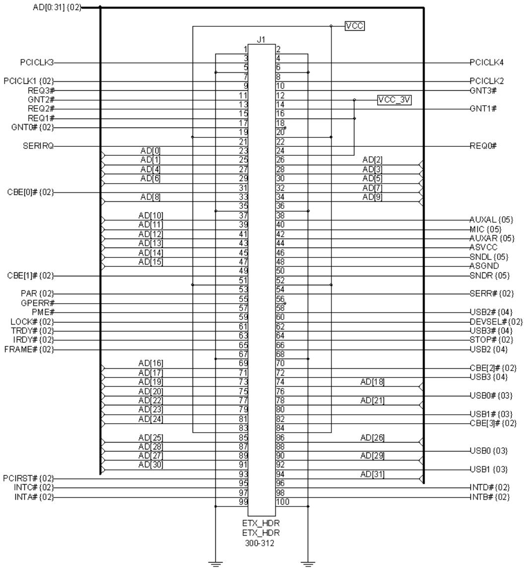
Figure 1 – ETX® Connector X1 Schematic

3.2 ETX® Connector X1 Pinout

<table><tr><td>Pin</td><td>Signal</td><td>Pin</td><td>Signal</td><td></td><td>Pin</td><td>Signal</td><td>Pin</td><td>Signal</td></tr><tr><td>1</td><td>GND</td><td>2</td><td>GND</td><td></td><td>51</td><td>VCC</td><td>52</td><td>VCC</td></tr><tr><td>3</td><td>PCICLK3</td><td>4</td><td>PCICLK4</td><td></td><td>53</td><td>PAR</td><td>54</td><td>SERR#</td></tr><tr><td>5</td><td>GND</td><td>6</td><td>GND</td><td></td><td>55</td><td>GPERR#</td><td>56</td><td>RESERVED</td></tr><tr><td>7</td><td>PCICLK1</td><td>8</td><td>PCICLK2</td><td></td><td>57</td><td>PME#</td><td>58</td><td>USB2#</td></tr><tr><td>9</td><td>REQ3#</td><td>10</td><td>GNT3#</td><td></td><td>59</td><td>LOCK#</td><td>60</td><td>DEVSEL#</td></tr><tr><td>11</td><td>GNT2#</td><td>12</td><td>3V</td><td></td><td>61</td><td>TRDY#</td><td>62</td><td>USB3#</td></tr><tr><td>13</td><td>REQ2#</td><td>14</td><td>GNT1#</td><td></td><td>63</td><td>IRDY#</td><td>64</td><td>STOP#</td></tr><tr><td>15</td><td>REQ1#</td><td>16</td><td>3V</td><td></td><td>65</td><td>FRAME#</td><td>66</td><td>USB2</td></tr><tr><td>17</td><td>GNT0#</td><td>18</td><td>RESERVED</td><td></td><td>67</td><td>GND</td><td>68</td><td>GND</td></tr><tr><td>19</td><td>VCC</td><td>20</td><td>VCC</td><td></td><td>69</td><td>AD16</td><td>70</td><td>CBE2#</td></tr><tr><td>21</td><td>SERIRQ</td><td>22</td><td>REQ0#</td><td></td><td>71</td><td>AD17</td><td>72</td><td>USB3</td></tr><tr><td>23</td><td>AD0</td><td>24</td><td>3V</td><td></td><td>73</td><td>AD19</td><td>74</td><td>AD18</td></tr><tr><td>25</td><td>AD1</td><td>26</td><td>AD2</td><td></td><td>75</td><td>AD20</td><td>76</td><td>USB0#</td></tr><tr><td>27</td><td>AD4</td><td>28</td><td>AD3</td><td></td><td>77</td><td>AD22</td><td>78</td><td>AD21</td></tr><tr><td>29</td><td>AD6</td><td>30</td><td>AD5</td><td></td><td>79</td><td>AD23</td><td>80</td><td>USB1#</td></tr><tr><td>31</td><td>CBE0#</td><td>32</td><td>AD7</td><td></td><td>81</td><td>AD24</td><td>82</td><td>CBE3#</td></tr><tr><td>33</td><td>AD8</td><td>34</td><td>AD9</td><td></td><td>83</td><td>VCC</td><td>84</td><td>VCC</td></tr><tr><td>35</td><td>GND</td><td>36</td><td>GND</td><td></td><td>85</td><td>AD25</td><td>86</td><td>AD26</td></tr><tr><td>37</td><td>AD10</td><td>38</td><td>AUXAL</td><td></td><td>87</td><td>AD28</td><td>88</td><td>USB0</td></tr><tr><td>39</td><td>AD11</td><td>40</td><td>MIC</td><td></td><td>89</td><td>AD27</td><td>90</td><td>AD29</td></tr><tr><td>41</td><td>AD12</td><td>42</td><td>AUXAR</td><td></td><td>91</td><td>AD30</td><td>92</td><td>USB1</td></tr><tr><td>43</td><td>AD13</td><td>44</td><td>ASVCC</td><td></td><td>93</td><td>PCIRST#</td><td>94</td><td>AD31</td></tr><tr><td>45</td><td>AD14</td><td>46</td><td>SNDL</td><td></td><td>95</td><td>INTC#</td><td>96</td><td>INTD#</td></tr><tr><td>47</td><td>AD15</td><td>48</td><td>ASGND</td><td></td><td>97</td><td>INTA#</td><td>98</td><td>INTB#</td></tr><tr><td>49</td><td>CBE1#</td><td>50</td><td>SNDR</td><td></td><td>99</td><td>GND</td><td>100</td><td>GND</td></tr></table>

Signal names in the table can differ slightly from those in the schematic. For example, AD[12] in the schematic is shown as AD12 in the pinout table and in the ETX® Specification. These differences reflect the conventions used by the program used to produce the schematics.

# 3.3 Peripheral Component Interconnect (PCI) Bus

![The image is a schematic diagram of a connector labeled 'X5' at the top and 'IPCICON' at the bottom. It features a 120-pin connector symbol with pins numbered 1-60 on the right and 61-120 on the left.  **Text Inside the Connector Box (Pin Names):** *   **Right Column (Pins 1-60):**     1.  TRST     2.  +12V     3.  TMS     4.  TDI     5.  +5V     6.  INTA     7.  +5V     8.  NC     9.  NC     10. NC     11. NC     12. GND     13. GND     14. NC     15. RST     16. +5V     17. GNTJ0     18. GND     19. PMEJ     20. AD30     21. +3.3V     22. AD28     23. AD26     24. AD24     25. C/BE3     26. IDSEL0     27. +3.3V     28. AD22     29. AD20     30. GND     31. AD18     32. AD16     33. +3.3V     34. FRAMEJ     35. GND     36. TRDYJ     37. GND     38. STOPJ     39. +3.3V     40. SDONE     41. NC     42. NC     43. PAR     44. AD15     45. +3.3V     46. AD13     47. AD11     48. GND     49. AD9     50. C/BE0     51. +3.3V     52. AD6     53. AD4     54. GND     55. AD2     56. AD0     57. +5V     58. REQ64     59. +5V     60. +5V  *   **Left Column (Pins 61-120):**     61. -12V     62. TCK     64. VCC     66. +5V     67. +5V     69. PRSNT1_S1#     70. INTB     71. INTD     72. PRSNT1     73. PRSNT2     74. NC     75. NC     76. GND     77. GND     78. GND     79. REQ     80. AD31     81. AD29     82. GND     83. AD27     84. AD25     85. AD23     86. C/BE3     87. AD23     88. AD21     89. AD19     90. AD17     91. AD19 (Note: Text alignment suggests AD19, though outside label is AD17) -) Correction: Pin 91 inside is AD19. Wait, looking closely at crop 1, pin 91 inside is AD19. Pin 90 inside is AD17.     92. C/BE2     93. AD17 (Note: Text alignment suggests AD17, though outside label is AD17) -) Correction: Pin 93 inside is AD17.     94. GND     95. IRDY     96. +3.3V     97. DEVSEL     98. GND     99. LOCK     100. PERR     101. +3.3V     102. SERR     103. +3.3V     104. C/BE1     105. AD14     106. GND     107. AD12     108. AD10     109. GND     110. AD8     111. AD7     112. +3.3V     113. AD5     114. AD3     115. GND     116. AD1     117. +5V     118. ACK64     119. +5V     120. +5V  **Text Outside the Connector Box (Net Labels):** *   **Top/Left:** -12V, TCK, VCC, IRQX, IRQZ, PRSNT1_S1#, PRSNT2_S1#, PCICLK1, REQJ0, AD31, AD29, AD27, AD25, CBEJ3, AD23, AD21, AD19, AD17, CBEJ2, IRDYJ, DEVSELJ, LOCKJ, GPERRJ, SERRJ, CBEJ1, AD14, AD12, AD10, AD8, AD7, AD5, AD3, AD1, ACK64J_0, 3V_ATX. *   **Top/Right:** VCC, TRST, +12V, TMS, TDI, IROWV, IRQY, PCIRSTJ, GNTJ0, PMEJ, AD30, AD28, AD26, AD24, IDSEL0, AD22, AD20, AD18, AD16, FRAMEJ, TRDYJ, STOPJ, SDONE, PAR, AD13, AD11, AD9, C/BE0, AD6, AD4, AD2, AD0, REQ64J_0. *   **Bottom:** GND (appears three times at the bottom).  **Components:** *   Capacitors: C86 C100n05, C85 C100n05. *   Ground symbols (GND) connected to capacitors and pins. *   'x' marks on pins 10, 14, 41, 42, 65, 71, 74.](.etx-design-guide-rev2-4/cc8054863f89747ccdce3126ae5f949fff73d9bdf6d2d080ea2e7310027c47f1.jpg)
Figure 2 – PCI Bus Slot Connector – Slot 1
Figure 2 shows a single PCI bus slot connector. You can connect up four PCI slots or external PCI devices to an ETX® module.

# 3.3.1 PCI Implementation Notes

➤ If a PC104-Plus connector is used, the same signals are attached to the connector but the pin numbers differ because of the different connector type. See the PC/104 Bus Version 2.3, June 1996, PC/104 Consortium (www.pc104.ord) for details.
➤ A PCI device implemented directly on the baseboard uses a subset of the signals shown on the slot connector. Some pins on the slot connector are used for slot and PCI card management functions and are not necessary for the operation of the PCI device itself. An individual PCI device will not have pins REQ64, ACK64, M66EN, PRSNT1, PRSNT2, SDONE, SBO#, or the reserved pins.
➤ Most devices do not implement the test pins TCK, TDO, TDI, TMS, and TRST.
➤ Most PCI devices use INTA# only and do not have a connection for INTB#, INTC# or INTD#. However, the INTA# pin of the device should not necessarily be connected to the ETX® INTA# signal. See the following interrupt section for details.

# 3.3.2 Differences Among PCI Slots

Most PCI signals are connected in parallel to all the slots (or devices). The exceptions are the following pins from each slot or device:

➤ IDSEL – Connected (through resistor) to a different AD line for each slot.
➤ CLK – Connected to a different ETX® PCI clock signal for each slot.
➤ INTA# - Connected to a different ETX® interrupt signal for each slot.
➤ REQ# - Connected to a different ETX® request signal for each slot, if used.
➤ GNT# - Connected to a different ETX® grant signal for each slot, if used.

Each signal connects differently for each of the four possible slots or devices as summarized in the following PCI Slots/Devices table:

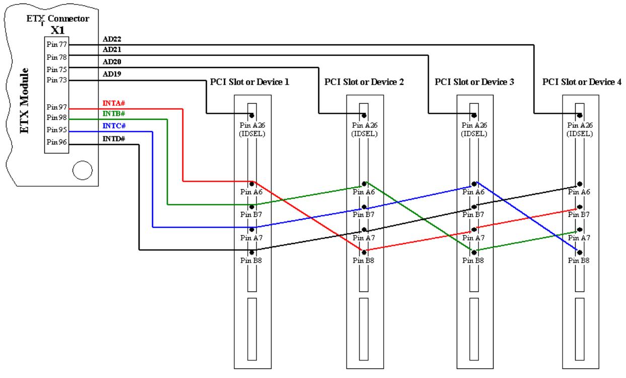
Note: The naming convention of the PCI interrupt signal and the interrupt pin on the PCI slot/device is the same. Pay attention to the routing of these signals. Check the example below for a better understanding.

<table><tr><td>Signal from ETX®</td><td>PCI Slot or PCI Device 1</td><td>PCI Slot or PCI Device 2</td><td>PCI Slot or PCI Device 3</td><td>PCI Slot or PCI Device 4</td></tr><tr><td>Signal AD19(X1 Pin 73)</td><td>Pin Name IDSEL(Pin A26 on PCI Slot)</td><td>-</td><td>-</td><td>-</td></tr><tr><td>Signal AD20(X1 Pin 75)</td><td>-</td><td>Pin Name IDSEL(Pin A26 on PCI Slot)</td><td>-</td><td>-</td></tr><tr><td>Signal AD21(X1 Pin 78)</td><td>-</td><td>-</td><td>Pin Name IDSEL(Pin A26 on PCI Slot)</td><td>-</td></tr><tr><td>Signal AD22(X1 Pin 77)</td><td>-</td><td>-</td><td>-</td><td>Pin Name IDSEL(Pin A26 on PCI Slot)</td></tr><tr><td>Signal INTA#(X1 Pin 97)</td><td>Pin Name INTA#(Pin A6 on PCI Slot)</td><td>Pin Name INTD# * (Pin B8 on PCI Slot)</td><td>Pin Name INTC# * (Pin A7 on PCI Slot)</td><td>Pin Name INTB# * (Pin B7 on PCI Slot)</td></tr><tr><td>Signal INTB#(X1 Pin 98)</td><td>Pin Name INTB# * (Pin B7 on PCI Slot)</td><td>Pin Name INTA#(Pin A6 on PCI Slot)</td><td>Pin Name INTD# * (Pin B8 on PCI Slot)</td><td>Pin Name INTC# * (Pin A7 on PCI Slot)</td></tr><tr><td>Signal INTC#(X1 Pin 95)</td><td>Pin Name INTC# * (Pin A7 on PCI Slot)</td><td>Pin Name INTB# * (Pin B7 on PCI Slot)</td><td>Pin Name INTA#(Pin A6 on PCI Slot)</td><td>Pin Name INTD# * (Pin B8 on PCI Slot)</td></tr><tr><td>Signal INTD#(X1 Pin 96)</td><td>Pin Name INTD# * (Pin B8 on PCI Slot)</td><td>Pin Name INTC# * (Pin A7 on PCI Slot)</td><td>Pin Name INTB# * (Pin B7 on PCI Slot)</td><td>Pin Name INTA#(Pin A6 on PCI Slot)</td></tr></table>

Note: \*Multifunction PCI devices require that this pin be connected.

Example: Using 4 PCI Slots on the Backplane
![Based on the provided flowchart/block diagram, here are the labeled blocks and their connections:  **Labeled Blocks:**  1.  **ETX Module (Connector X1)**     *   Contains pins: **Pin 77** (**AD22**), **Pin 78** (**AD21**), **Pin 75** (**AD20**), **Pin 73** (**AD19**), **Pin 97** (**INTA#**), **Pin 98** (**INTB#**), **Pin 95** (**INTC#**), **Pin 96** (**INTD#**). 2.  **PCI Slot or Device 1**     *   Contains pins: **Pin A26 (IDSEL)**, **Pin A6**, **Pin B7**, **Pin A7**, **Pin B8**. 3.  **PCI Slot or Device 2**     *   Contains pins: **Pin A26 (IDSEL)**, **Pin A6**, **Pin B7**, **Pin A7**, **Pin B8**. 4.  **PCI Slot or Device 3**     *   Contains pins: **Pin A26 (IDSEL)**, **Pin A6**, **Pin B7**, **Pin A7**, **Pin B8**. 5.  **PCI Slot or Device 4**     *   Contains pins: **Pin A26 (IDSEL)**, **Pin A6**, **Pin B7**, **Pin A7**, **Pin B8**.  **Connections:**  *   **AD Lines (Black):**     *   **Pin 77 (AD22)** connects to **PCI Slot or Device 4 (Pin A26)**.     *   **Pin 78 (AD21)** connects to **PCI Slot or Device 3 (Pin A26)**.     *   **Pin 75 (AD20)** connects to **PCI Slot or Device 2 (Pin A26)**.     *   **Pin 73 (AD19)** connects to **PCI Slot or Device 1 (Pin A26)**.  *   **INT Lines (Color-coded):**     *   **INTA# (Red):** Connects **Pin 97** to **PCI Slot or Device 1 (Pin A6)**, then to **PCI Slot or Device 2 (Pin B8)**, then to **PCI Slot or Device 3 (Pin A7)**, and finally to **PCI Slot or Device 4 (Pin B7)**.     *   **INTB# (Green):** Connects **Pin 98** to **PCI Slot or Device 1 (Pin B7)**, then to **PCI Slot or Device 2 (Pin A6)**, then to **PCI Slot or Device 3 (Pin B8)**, and finally to **PCI Slot or Device 4 (Pin A7)**.     *   **INTC# (Blue):** Connects **Pin 95** to **PCI Slot or Device 1 (Pin A7)**, then to **PCI Slot or Device 2 (Pin B7)**, then to **PCI Slot or Device 3 (Pin A6)**, and finally to **PCI Slot or Device 4 (Pin B8)**.     *   **INTD# (Black):** Connects **Pin 96** to **PCI Slot or Device 1 (Pin B8)**, then to **PCI Slot or Device 2 (Pin A7)**, then to **PCI Slot or Device 3 (Pin B7)**, and finally to **PCI Slot or Device 4 (Pin A6)**.](.etx-design-guide-rev2-4/f8264cdfd69322c7f2ad325acf3af43ac9ee450b955bdfa2ae55c7e1d2afa6e9.jpg)

Figure 3 - PCI interrupt routing

# IDSEL

➤ Connect each slot or device IDSEL pin to an appropriate AD line via a 22-Ohm resistor.

# PCICLK

➤ The trace length for all PCI clocks should be matched and controlled. PCI clock routes should be separated as far from other signal traces as possible.
➤ PCI clock signals should be routed as controlled-impedance traces, with trace impedance in the 60-70 Ohm range.
➤ Only one PCI device or slot should be driven from each ETX® PCI clock output.
➤ The PCICLK signal that comes from the ETX® module is timed for an external trace delay of 1300pS from the ETX® output pin to the PCI device’s clock pin.
➤ The trace length from the ETX® clock pin to a PCI device on the baseboard should be about 8.7 inches (if a typical figure for baseboard PCB propagation delay of 150pS per inch is used). If a more accurate value is available for PCB propagation delay, it should be used in place of the 150pS/inch rule-of-thumb to calculate clock-trace lengths.
➤ The clock trace from the ETX® module pin to a slot connector clock pin should be about 2.5 inches shorter than the length to a device pin because PCI cards are specified to have 2.5 inches of onboard clock trace length from the connector pin to the device clock pin.

# INT

➤ PC104-Plus implementations also assume 2.5 inches of trace length on each module. In addition, further shorten clock routes for specific slot positions to account for varying stack positions of the PC104-Plus modules. See the PC104-Plus Specification for details.
➤ Most PCI devices implement only one interrupt, which is output on the INTA# pin. This should be connected to the INT inputs on the ETX® module as per the table. For multifunction devices, connect the additional interrupt outputs as per the table.
➤ PCI card slots or PC104-Plus implementations must have all four interrupt lines connected to each slot as per the table. Note that the interrupt wiring rotates for different slot positions.
➤ PCI specifications require that PCI devices be capable of interrupt sharing. Interrupts are typically shared in PCI systems that have more than four interrupt-generating devices. The purpose of the assignment scheme shown in the table is to distribute the devices as evenly as possible over the four PCI interrupt lines.

# REQ/GNT

➤ These signals are used only by bus-mastering PCI devices. Most ETX® modules do not have enough REQ/GNT pairs available to support a bus-mastering device at every slot position. Refer to the individual ETX® user’s guide for details.
➤ If there are less than four REQ/GNT pairs available for external devices, they will be assigned starting with the REQ0#/GNT0# pair. Therefore, external bus-mastering devices should be placed in the lowest numbered slot positions and non-bus mastering devices should be placed in the highest-numbered slot positions.

# 3.4 Universal Serial Bus (USB)

# 3.4.1 USB Port 0 and 1
![VCC_USB0 (THIS SHEET) FB1 50 @ 100MHz 3A S1206 C6 0.01UF S0603 J7 9 USB0# {01} 7 USB0 {01} 6 C3 100UF S7343 + FB2 50 @ 100MHz 3A S1206 GND_USB0 5 C7 0.01UF S0603 J7 10 VCC_USB1 (THIS SHEET) FB3 50 @ 100MHz 3A S1206 VCC_USB1_EXT 4 C8 0.01UF S0603 J7 11 USB1# {01} 3 USB1 {01} 2 C4 100UF S7343 + FB4 50 @ 100MHz 3A S1206 GND_USB1 1 C9 0.01UF S0603 USB DUAL 87525-0001 J7 OVCR# {04,16} U1 8 EN1# 3 EN2# 4 OC2# 5 TPS2042 SO8 IN 2 OUT1 7 OUT2 6 GND 1 VCC VCC_USB0 (THIS SHEET) VCC_USB1 (THIS SHEET)](.etx-design-guide-rev2-4/4a0f0ed5a2fba2b7088016fe55179ee00c3f0a244d2fe7f7b9eeff9fa9bea696.jpg)

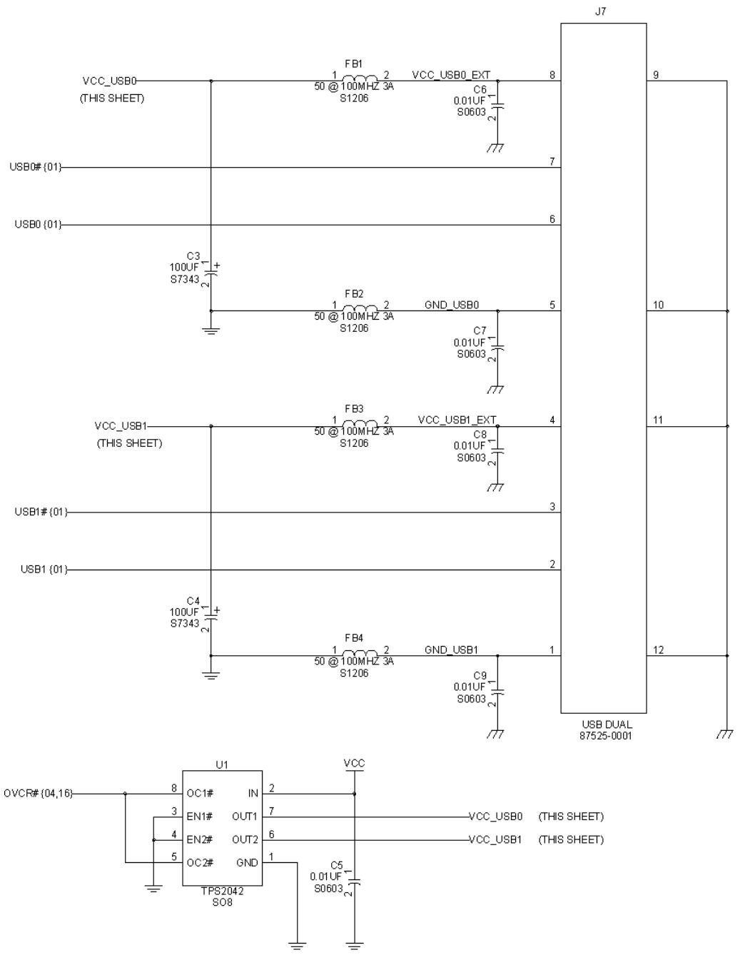
Figure 4 – USB Port 0 & 1

The TPS2042 chip shown provides overcurrent protection for each USB port. Either or both of the OC# outputs may be connected as desired so that software running on the ETX® module can sense an overcurrent condition on one or both USB ports.

# 3.4.2 USB Ports 2 and 3
![VCC_USB2 (THIS SHEET) FB5 1 2 VCC_USB2_EXT 8 50 @ 100MHz 3A C13 S1206 0.01UF S0603 1 77 USB2#{01} 7 USB2{01} C10 100UF S7343 + FB6 1 2 GND_USB2_EXT 5 50 @ 100MHz 3A C14 S1206 0.01UF S0603 1 77 VCC_USB3 (THIS SHEET) FB7 1 2 VCC_USB3_EXT 4 50 @ 100MHz 3A C15 S1206 0.01UF S0603 1 77 USB3#{01} 3 USB3{01} 2 C11 100UF S7343 + FB8 1 2 GND_USB3_EXT 1 50 @ 100MHz 3A C16 S1206 0.01UF S0603 1 77 USB DUAL 87525-0001 J8 9 10 11 12 OVCR#{03,16} U2 8 OC1# 3 EN1# OUT1 2 VCC 4 EN2# OUT2 7 VCC_USB2 (THIS SHEET) 5 OC2# GND 6 VCC_USB3 (THIS SHEET) TPS2042 SO8 C12 1 S0603](.etx-design-guide-rev2-4/14e0bb5fa12a4de233ca152ad740cfc41981d7597245859c64d0d2e4c2b8a5c0.jpg)

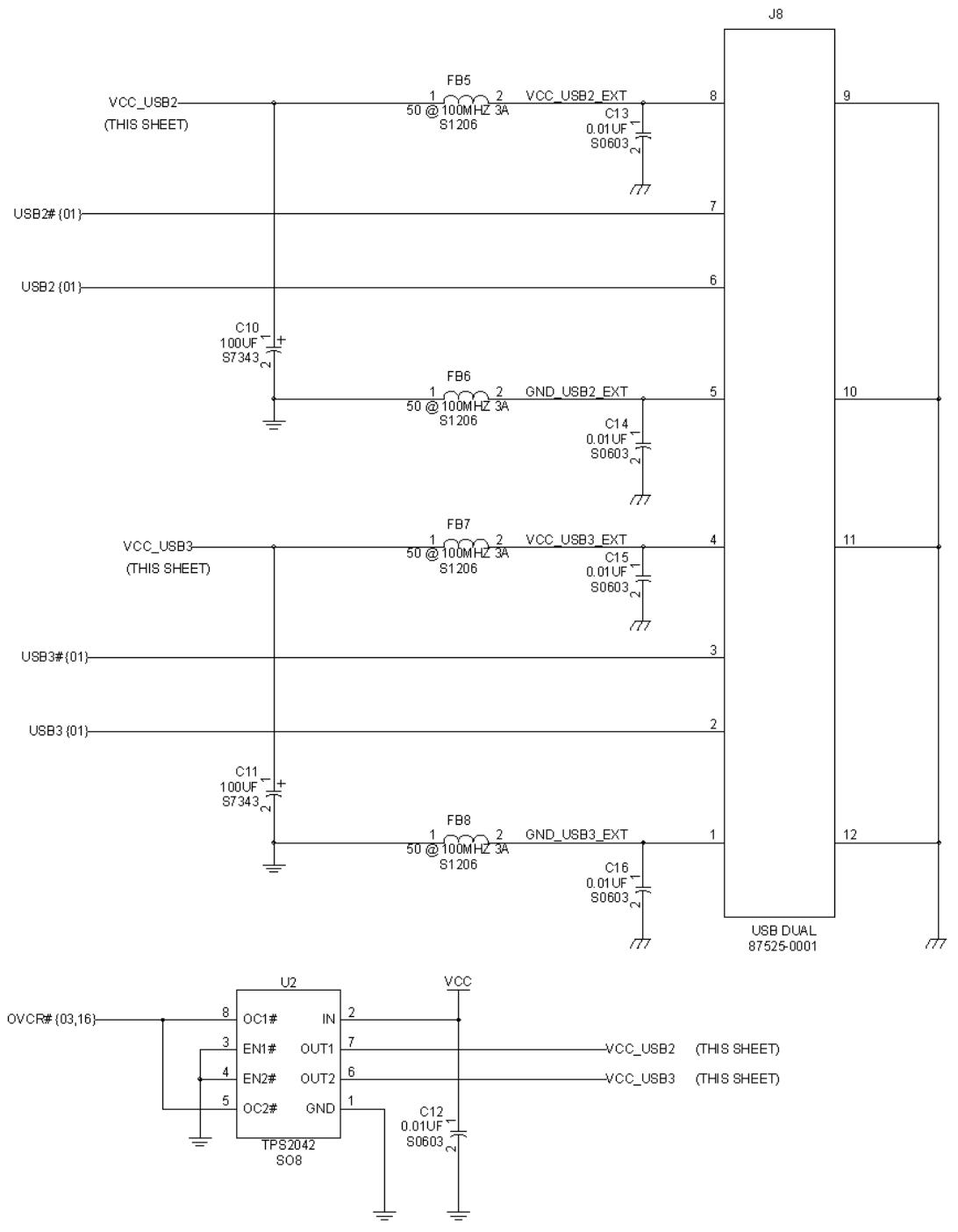
Figure 5 – USB Port 2 & 3

The TPS2042 chip provides overcurrent protection for each USB port. You can connect either or both OC# outputs so that software running on the ETX® module can sense an overcurrent condition on one or both USB ports.

# 3.4.3 USB Implementation Notes

➤ The USB data pairs (USB0 and US0#) should be routed on the baseboard as differential pairs, with a differential impedance of 90 Ohms. PCB layout software usually allows determining the correct trace width and spacing to achieve this impedance, after the PCB stackup configuration is known.
➤ As per usual differential pair routing practices, the two traces of each USB pair should be matched in length and kept at uniform spacing. Sharp corners should be avoided. At the ETX® module and connector ends of the routes, loop areas should be minimized.
➤ USB data pairs should be routed as far from other signals as possible.
➤ Overcurrent protection on external USB power lines is required to prevent faults in external USB devices or cables from causing hardware damage and/or crashing the system. Note that overcurrent protection devices typically allow relatively high currents to flow for brief periods before the current is limited or interrupted. The system power supply must be able to provide these high currents while maintaining output regulation, or else the ETX® module or other system components may malfunction.
➤ You can “hot plug” USB devices. In fact, this is one of the virtues of USB relative to most other PC interfaces. The design of the USB power-decoupling network must absorb the momentary current surge from hot-plugging an unpowered device. This is the reason for the large capacitance values of C10 and C11 in the reference schematic. Reducing these values is not recommended.
➤ ETX® modules vary in the number of USB ports that are implemented. Two ports are typical. Some ETX® modules implement three or four ports. If the application needs more than two USB ports, a low-cost USB hub IC can be integrated onto the baseboard and connected to the USB0 or USB1 ports on the ETX® module. This provides a larger number of USB ports regardless of which ETX® module is in use.
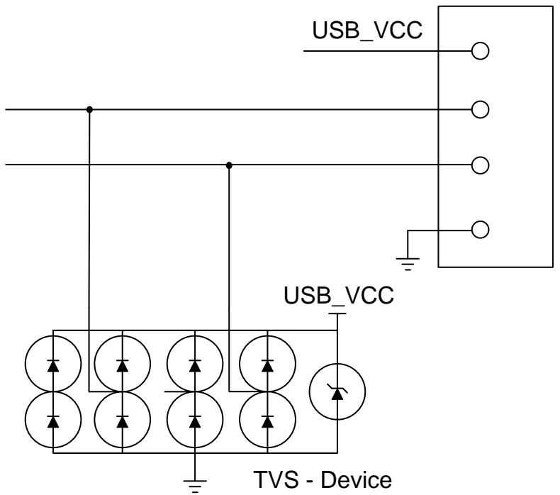
➤ Some USB designs will need additional ESD or EMI suppression components on the USB data lines. These are most effective when they are placed near the external USB connector and grounded to a low-impedance ground plane.

ESD measures
![USB_VCC USB_VCC TVS - Device](.etx-design-guide-rev2-4/d405f5342dba3c6e0b476fcb9ae77ed64ea09be4242e608c979321eb1269f20b.jpg)

Figure 6 – USB ESD measures

We recommend mounting right near the USB connector a USB TVS device to avoid ESD disturbances.

Possible devices are e.g. Philips IP4220CZ6 or Semtech SRV05-4

# 3.4.4 USB Signal Integrity

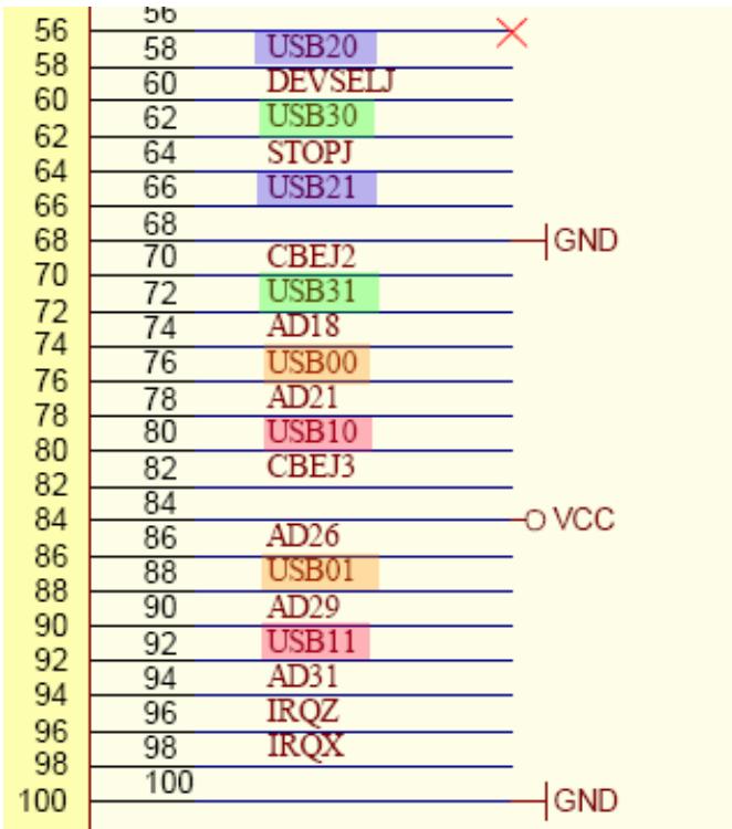
When ETX was specified the first time it was in 1999 when only USB 1.1 LowSpeed/FullSpeed was available. The pining of USB on the ETX connectors was quite uncritical and therefore it was done like that on X1.
![  Position   Bit Position   Label    --- --- ---    56   56       58   58   USB20     60   60   DEVSELJ     62   62   USB30     64   64   STOPJ     66   66   USB21     68   68       70   70   CBEJ2     72   72   USB31     74   74   AD18     76   76   USB00     78   78   AD21     80   80   USB10     82   82   CBEJ3     84   84       86   86   AD26     88   88   USB01     90   90   AD29     92   92   USB11     94   94   AD31     96   96   IRQZ     98   98   IRQX     100   100     X GND ○VCC GND](.etx-design-guide-rev2-4/8acb9f59fa679aa44355d3854bbf0d64657f13ca410f7c04881ab674acb84227.jpg)

The differential pair signals of each USB line are separated end routed to pins of connector X1 which are not close to each other. The effect could be that the signal integrity is disturbed, the longer the separated way of signal trace is. Therefore the high ETX baseboard connectors (Hirose FX8C-100S-SV5) might create more problems than low ones regarding USB 2.0 HighSpeed.

# 3.5 Audio Circuits
![This is a schematic diagram for an audio circuit, featuring a power amplifier section and multiple input/output connectors.  **Power and Amplifier Section (Top):** *   **Power Input:** A `+12V` source connects through inductor `FB9` (50 @ 100MHZ 3A, S1206) to the `VCC_AUDIO_PA` rail. Capacitor `C20` (470UF 16V, CPAN_G) filters this rail. *   **IC (U3):** The central component is a `TPA1517NE` amplifier in a `DIP20` package. A note specifies: 'DIP PINOUT ONLY! PINS 10 AND 11 MISSING ON PHILIPS TDA1517P'. Another note states: 'NOTE: NON-THERMAL VIAS MUST BE PROVIDED ON PIN 10 AND PINS 11-20'.     *   **Inputs:** `IN1` (Pin 1) receives `SNDR (01)` through capacitor `C17` (0.1UF, S0805). `IN2` (Pin 9) receives `SNDL (01)` through capacitor `C18` (0.1UF, S0805). `SVRR` (Pin 3) connects to ground via `C19` (220UF 16V, CPAN_F).     *   **Ground Pins:** Pins 11 through 20 (labeled `GND/HS6` through `GND/HS10`) are all connected to ground.     *   **Mode Select:** `M/SB` (Pin 8) connects to ground via resistor `R2` (10K, S0603) and an unpopulated resistor `R3` (OPEN, S0603).     *   **Outputs:** `OUT1` (Pin 4) and `OUT2` (Pin 6) drive the speaker lines.  **Speaker Outputs (Right):** *   **Right Channel:** `OUT1` connects to `R_SPEAK_CC`, which splits. One path goes through capacitor `C22` (220UF 16V, CPAN_F) to `R_SPEAK`, then through inductor `FB15` (50 @ 100MHZ 3A, S1206) to Pin 5 (TIP) of connector `J12`. A filter network (`C21` 0.1UF, `R4` 22) connects `R_SPEAK_CC` to ground. *   **Left Channel:** `OUT2` connects to `L_SPEAK_CC`, which splits. One path goes through capacitor `C23` (220UF 16V, CPAN_F) to `L_SPEAK`, then through inductor `FB16` (50 @ 100MHZ 3A, S1206) to Pin 4 (SWT) of connector `J12`. A filter network (`C24` 0.1UF, `R5` 22) connects `L_SPEAK_CC` to ground. *   **Connector J12:** Labeled '3.5MM PHONE JY3540' with pins: 1 SLV, 2 RNG, 3 SWR, 4 SWT, 5 TIP.  **Input Connectors (Bottom):** *   **Microphone (J9):** Labeled '3.5MM PHONE JY3540'. Signal `MIC (01)` goes through inductor `FB10` (120 ohm @ 100MHz, S0603) to Pin 5 (TIP). *   **Line In (J10):** Labeled '3.5MM PHONE JY3540'. Signal `AUXAR (01)` goes through inductor `FB11` (120 ohm @ 100MHz, S0603) to Pin 1 (SLV). Signal `AUXAL (01)` goes through inductor `FB12` (120 ohm @ 100MHz, S0603) to Pin 5 (TIP). *   **Line Out (J11):** Labeled '3.5MM PHONE JY3540'. Signal `SNDR (01)` goes through inductor `FB13` (120 ohm @ 100MHz, S0603) to Pin 1 (SLV). Signal `SNDL (01)` goes through inductor `FB14` (120 ohm @ 100MHz, S0603) to Pin 5 (TIP).](.etx-design-guide-rev2-4/75e00dd32269be9bf8ae21577a84959580caf8a5e3693b0103eec9541a0730a5.jpg)
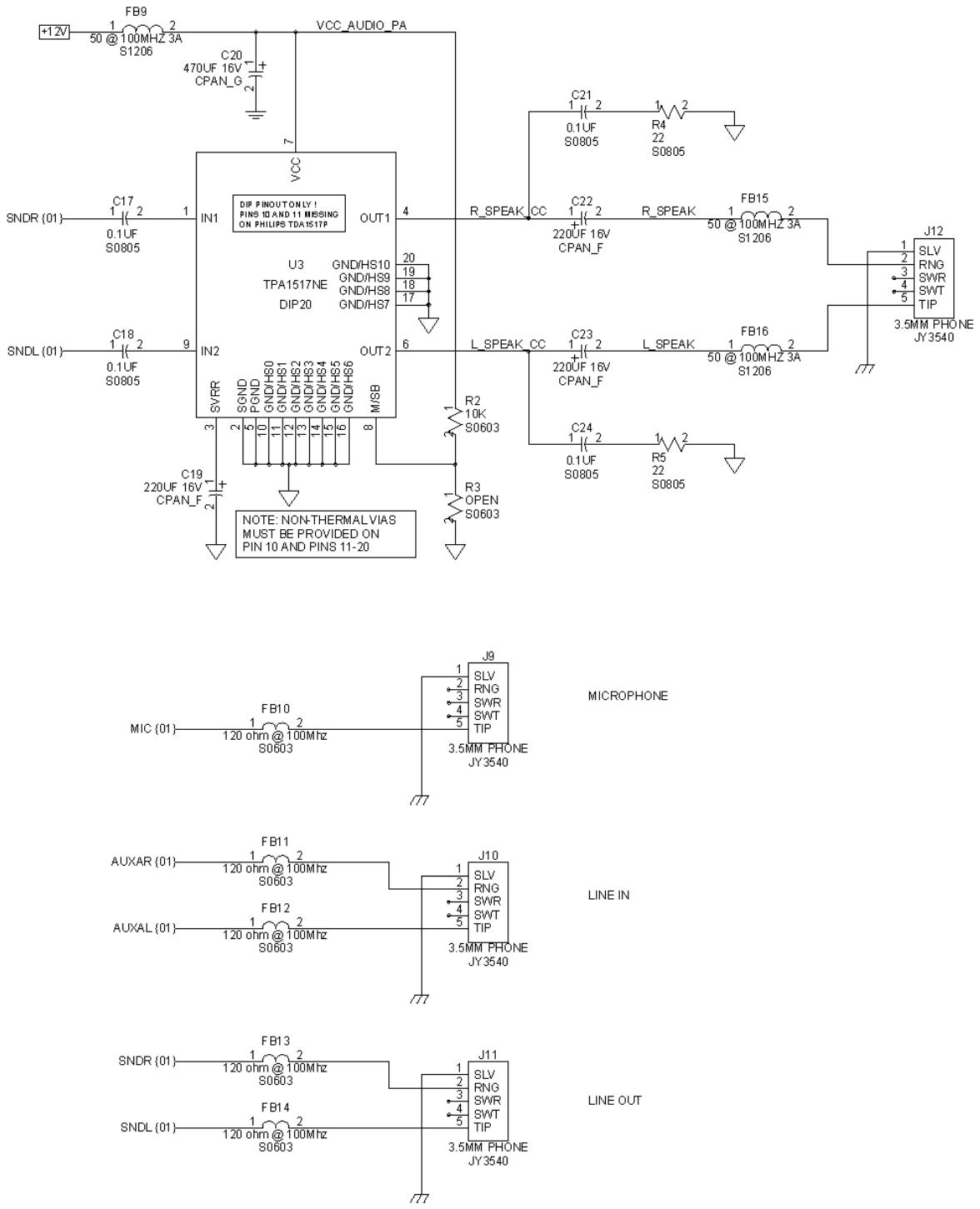
Figure 7 – Audio Circuits

The top section of Figure 7 shows one possible audio amplifier circuit for use with an ETX® module. This circuit uses a low-cost DIP amplifier made by Texas Instruments and Philips. This circuit requires a 12- volt supply.

Many other audio amplifier IC’s exist. Some circuits can operate from lower supply voltages and/or do not require output capacitors. Representative manufacturers of such amplifiers are National Semiconductor and Texas Instruments.

The lower section of Figure 5 shows ETX® connections that implement microphone, line in, and line out functions using standard 3.5mm phone jacks.

# 3.5.1 Audio Implementation Notes

➤ All audio circuits require careful PCB layout and grounding to avoid picking up digital noise on audio-signal lines. The X1 connector has an audio ground pin (ASGND, pin 48) that should be connected to an analog ground plane underneath the audio amplifier circuits or the audio input/output jacks. This plane should be isolated from the ground plane that is used for digital circuitry. Rout audio signals over the analog ground plane wherever possible and keep them as far away as possible from digital signals.
➤ The AUX (line in) and SND (line out) signals are AC-coupled and have a maximum signal level of approximately 1V P-P. The line outputs are capable of driving a 5K Ohm load. Audio sources connected to line inputs should also be capable of driving a 5K Ohm load.
➤ The MIC (microphone input) is intended for a monaural electret microphone. In addition to the audio signal, this input carries a DC voltage of approximately 2.5V, which is sourced from 5K Ohm effective impedance. Many microphones use this DC voltage as a power source.
➤ Some ETX® modules provide an option for selecting additional preamplifier gain on the microphone input, while others provide only a single microphone gain setting. Designers should consider this in designing baseboards for microphone applications that are intended to work with different ETX® modules.
➤ For applications that require a stereo microphone or higher quality microphone audio, an external microphone preamplifier should be implemented on the baseboard and connected to the AUXAL/AUXAR inputs.
➤ If the AUXAL/AUXAR inputs are connected to the audio output from a CD-ROM drive, shielded cables should be used. The audio grounds from the CD-ROM audio cable should be connected to ASGND rather than to digital ground to minimize noise.

# 4 Connector X2

# 4.1 ETX® Connector X2 Schematic
![This is a schematic diagram of a connector labeled **J2**, showing pin assignments for an ETX_HDR (part number 300-312). The diagram lists signal names on the left and right sides, connected to pins numbered 1 through 100.  **Left Side Signals:** *   **SD(14)** (Pin 3) *   **SD(13)** (Pin 5) *   **SD(12)** (Pin 7) *   **SD(11)** (Pin 9) *   **SD(10)** (Pin 11) *   **SD(9)** (Pin 13) *   **SD(8)** (Pin 15) *   Group label: **SD(0:15){07}** *   **MEMW#{07}** (Pin 17) *   **MEMR#{07}** (Pin 19) *   **SA(17)** (Pin 21) *   **SA(18)** (Pin 23) *   **SA(19)** (Pin 25) *   **SA(20)** (Pin 27) *   **SA(21)** (Pin 29) *   **SA(22)** (Pin 31) *   **SA(23)** (Pin 33) *   Group label: **SA(17:23){07}** *   **SBHE#{07}** (Pin 35) *   **SA(0)** (Pin 39) *   **SA(1)** (Pin 41) *   **SA(2)** (Pin 43) *   **SA(3)** (Pin 45) *   **SA(4)** (Pin 47) *   **SA(5)** (Pin 49) *   **SA(6)** (Pin 53) *   **SA(7)** (Pin 55) *   **SA(8)** (Pin 57) *   **SA(9)** (Pin 59) *   **SA(10)** (Pin 61) *   **SA(11)** (Pin 63) *   **SA(12)** (Pin 65) *   Group label: **SA(0:19){07}** *   Note: **NOTE: SA(17) IS ON PIN 78** *   **SA(13)** (Pin 69) *   **SA(14)** (Pin 71) *   **SA(15)** (Pin 73) *   **SA(16)** (Pin 75) *   **SA(18)** (Pin 77) *   **SA(19)** (Pin 79) *   **IOCHRDY{07}** (Pin 81) *   **SD(0)** (Pin 85) *   **SD(2)** (Pin 87) *   **SD(3)** (Pin 89) *   **SD(5)** (Pin 91) *   **SD(6)** (Pin 93) *   **DRQ2{07}** (Pin 95) *   **IOCHK#{07}** (Pin 97)  **Right Side Signals:** *   **VCC** (Pin 2) *   **SD(15)** (Pin 4) *   **MASTER#{07}** (Pin 8) *   **DREQ7{07}** (Pin 10) *   **DACK7#{07}** (Pin 12) *   **DREQ6{07}** (Pin 14) *   **DACK6#{07}** (Pin 16) *   **DREQ5{07}** (Pin 18) *   **DACK5{07}** (Pin 20) *   **DREQ0{07}** (Pin 22) *   **DACK0{07}** (Pin 24) *   **IRQ14{07}** (Pin 26) *   **IRQ15{07}** (Pin 28) *   **IRQ12{07}** (Pin 30) *   **IRQ11{07}** (Pin 32) *   **IRQ10{07}** (Pin 34) *   **IO16#{07}** (Pin 36) *   **M16#{07}** (Pin 38) *   **OSC{07}** (Pin 40) *   **BALE{07}** (Pin 42) *   **TC{07}** (Pin 44) *   **DACK2#{07}** (Pin 46) *   **IRQ3{07}** (Pin 48) *   **IRQ4{07}** (Pin 50) *   **IRQ5{07}** (Pin 54) *   **IRQ6{07}** (Pin 56) *   **IRQ7{07}** (Pin 58) *   **SYSCLK{07}** (Pin 60) *   **REF SH#{07}** (Pin 62) *   **DREQ1{07}** (Pin 64) *   **DACK1#{07}** (Pin 66) *   **DREQ3{07}** (Pin 70) *   **DACK3#{07}** (Pin 72) *   **IOR#{07}** (Pin 74) *   **IOW#{07}** (Pin 76) *   **SA(17){07}** (Pin 78) *   **SMEMR#{07}** (Pin 80) *   **AEN{07}** (Pin 82) *   **SD(1)** (Pin 88) *   **NOSW#{07}** (Pin 90) *   **SD(4)** (Pin 92) *   **RSTDRV{07}** (Pin 98)  **Bottom Text:** *   **ETX_HDR** *   **ETX_HDR** *   **300-312**](.etx-design-guide-rev2-4/03eebac95105f1951448cb36595d4468b49be878ded76b37c61bf51ca8c9f6d7.jpg)
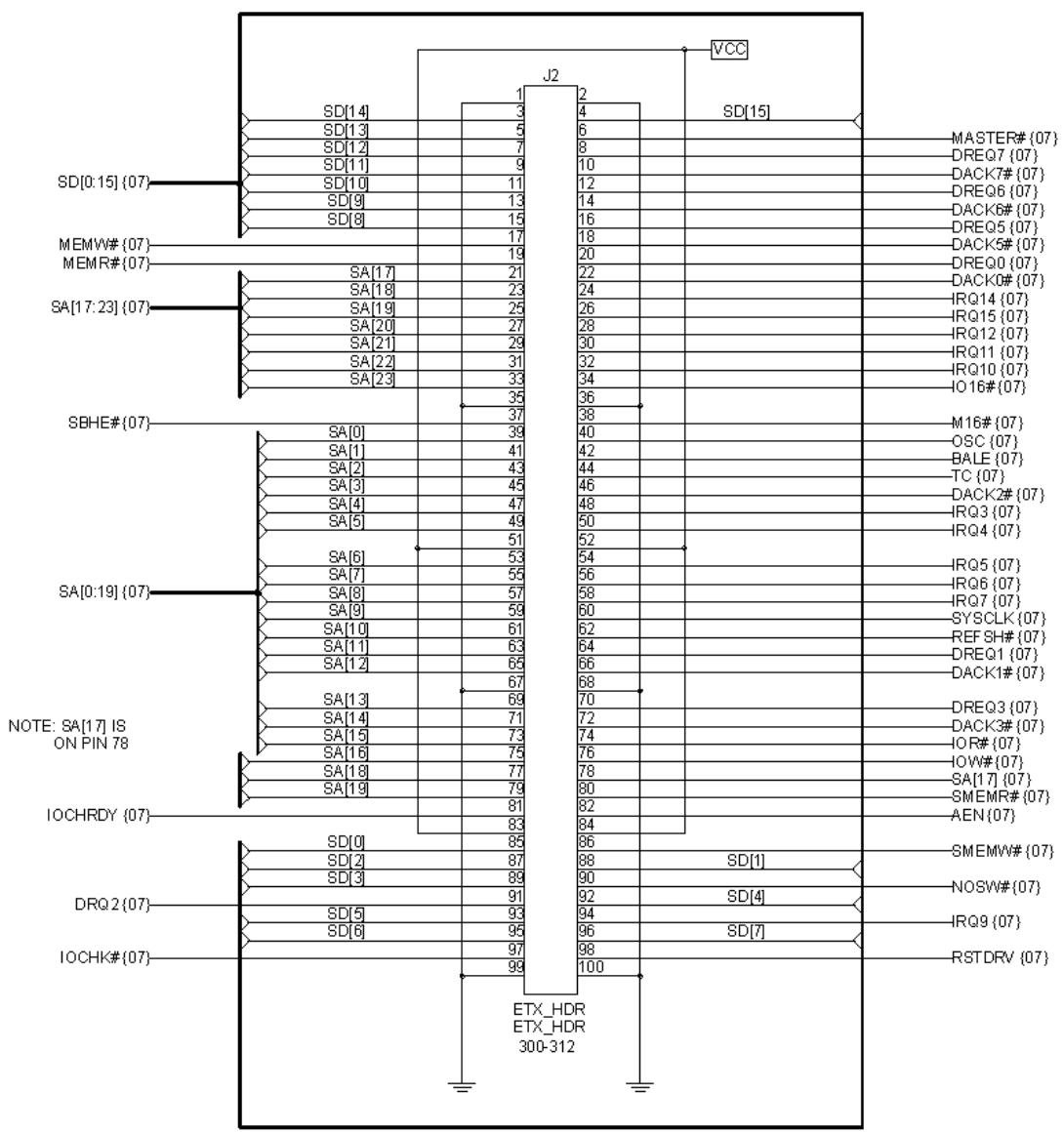
Figure 8 – ETX® Connector X2 Schematic

4.2 ETX® Connector X2 Pinout

<table><tr><td>Pin</td><td>Signal</td><td>Pin</td><td>Signal</td><td></td><td>Pin</td><td>Signal</td><td>Pin</td><td>Signal</td></tr><tr><td>1</td><td>GND</td><td>2</td><td>GND</td><td></td><td>51</td><td>VCC</td><td>52</td><td>VCC</td></tr><tr><td>3</td><td>SD14</td><td>4</td><td>SD15</td><td></td><td>53</td><td>SA6</td><td>54</td><td>IRQ5</td></tr><tr><td>5</td><td>SD13</td><td>6</td><td>MASTER#</td><td></td><td>55</td><td>SA7</td><td>56</td><td>IRQ6</td></tr><tr><td>7</td><td>SD12</td><td>8</td><td>DREQ7</td><td></td><td>57</td><td>SA8</td><td>58</td><td>IRQ7</td></tr><tr><td>9</td><td>SD11</td><td>10</td><td>DACK7#</td><td></td><td>59</td><td>SA9</td><td>60</td><td>SYSCLK</td></tr><tr><td>11</td><td>SD10</td><td>12</td><td>DREQ6</td><td></td><td>61</td><td>SA10</td><td>62</td><td>REFSH#</td></tr><tr><td>13</td><td>SD9</td><td>14</td><td>DACK6#</td><td></td><td>63</td><td>SA11</td><td>64</td><td>DREQ1</td></tr><tr><td>15</td><td>SD8</td><td>16</td><td>DREQ5</td><td></td><td>65</td><td>SA12</td><td>66</td><td>DACK1#</td></tr><tr><td>17</td><td>MEMW#</td><td>18</td><td>DACK5#</td><td></td><td>67</td><td>GND</td><td>68</td><td>GND</td></tr><tr><td>19</td><td>MEMR#</td><td>20</td><td>DREQ0</td><td></td><td>69</td><td>SA13</td><td>70</td><td>DREQ3</td></tr><tr><td>21</td><td>LA17</td><td>22</td><td>DACK0#</td><td></td><td>71</td><td>SA14</td><td>72</td><td>DACK3#</td></tr><tr><td>23</td><td>LA18</td><td>24</td><td>IRQ14</td><td></td><td>73</td><td>SA15</td><td>74</td><td>IOR#</td></tr><tr><td>25</td><td>LA19</td><td>26</td><td>IRQ15</td><td></td><td>75</td><td>SA16</td><td>76</td><td>IOW#</td></tr><tr><td>27</td><td>LA20</td><td>28</td><td>IRQ12</td><td></td><td>77</td><td>SA18</td><td>78</td><td>SA17</td></tr><tr><td>29</td><td>LA21</td><td>30</td><td>IRQ11</td><td></td><td>79</td><td>SA19</td><td>80</td><td>SMEMR#</td></tr><tr><td>31</td><td>LA22</td><td>32</td><td>IRQ10</td><td></td><td>81</td><td>IOCHRDY</td><td>82</td><td>AEN</td></tr><tr><td>33</td><td>LA23</td><td>34</td><td>IO16#</td><td></td><td>83</td><td>VCC</td><td>84</td><td>VCC</td></tr><tr><td>35</td><td>GND</td><td>36</td><td>GND</td><td></td><td>85</td><td>SD0</td><td>86</td><td>SMEMW#</td></tr><tr><td>37</td><td>SBHE#</td><td>38</td><td>M16#</td><td></td><td>87</td><td>SD2</td><td>88</td><td>SD1</td></tr><tr><td>39</td><td>SA0</td><td>40</td><td>OSC</td><td></td><td>89</td><td>SD3</td><td>90</td><td>NOWS#</td></tr><tr><td>41</td><td>SA1</td><td>42</td><td>BALE</td><td></td><td>91</td><td>DREQ2</td><td>92</td><td>SD4</td></tr><tr><td>43</td><td>SA2</td><td>44</td><td>TC</td><td></td><td>93</td><td>SD5</td><td>94</td><td>IRQ9</td></tr><tr><td>45</td><td>SA3</td><td>46</td><td>DACK2#</td><td></td><td>95</td><td>SD6</td><td>96</td><td>SD7</td></tr><tr><td>47</td><td>SA4</td><td>48</td><td>IRQ3</td><td></td><td>97</td><td>IOCHK#</td><td>98</td><td>RSTDRV</td></tr><tr><td>49</td><td>SA5</td><td>50</td><td>IRQ4</td><td></td><td>99</td><td>GND</td><td>100</td><td>GND</td></tr></table>

Signal names in the table can differ slightly from those in the schematic. For example, SD[12] in the schematic is shown as SD12 in the pinout table and in the ETX® Specification. These differences reflect the conventions used by the program used to produce these schematics.

# 4.3 Industry Standard Architecture (ISA) Bus Slot

![SD(0:15) {06} SA(0:19) {06} AEN {06} IOCHRDY {06} IOCHI# {06} VCC B1 GND1 TOCHK A1 RSTDRV {06} B2 RESDRV SD7 A2 SD(7) B3 VCC1 SD6 A3 SD(6) IRQ9 {06} B4 IRQ9 SD5 A4 SD(5) NEG5V {20,21} B5 -5V SD4 A5 SD(4) DRQ2 {06} B6 DREQ2 SD3 A6 SD(3) NEG12V {02,20,21} B7 -12V SD2 A7 SD(2) NOSW# {06} B8 UWS SD1 A8 SD(1) +12V B9 +12V SD0 A9 SD(0) B10 GND2 IOCHRDY A10 SMEMW# {06} B11 SMEMW AEN A11 SMEMR# {06} B12 SMEMR SA19 A12 SA(19) IOW# {06} B13 TOW SA18 A13 SA(18) IOR# {06} B14 TOR SA17 A14 SA(17) DACK# {06} B15 DACK3 SA16 A15 SA(16) DREQ3 {06} B16 DREQ3 SA15 A16 SA(15) DACK1# {06} B17 DACK1 SA14 A17 SA(14) DREQ1 {06} B18 DREQ1 SA13 A18 SA(13) REFSH# {06} B19 REFSH SA12 A19 SA(12) SYSCLK {06} B20 SYSCLK SA11 A20 SA(11) IRQ7 {06} B21 IRQ7 SA10 A21 SA(10) IRQ6 {06} B22 IRQ6 SA9 A22 SA(9) IRQ5 {06} B23 IRQ5 SA8 A23 SA(8) IRQ4 {06} B24 IRQ4 SA7 A24 SA(7) IRQ3 {06} B25 IRQ3 SA6 A25 SA(6) DACK2# {06} B26 DACK2 SA5 A26 SA(5) TC {06} B27 TC SA4 A27 SA(4) BALE {06} B28 ALE SA3 B29 VCC2 SA2 A28 SA(3) OSC {06} B30 OSC SA1 A30 SA(1) B31 GND3 SA0 A31 SA(0) M16# {06} D1 MEMCST6 BHE C1 IO16# {06} D2 TOCSST6 LA23 C2 SA(23) IRQ10 {06} D3 IRQ10 LA22 C3 SA(22) IRQ11 {06} D4 IRQ11 LA21 C4 SA(21) IRQ12 {06} D5 IRQ12 LA20 C5 SA(20) IRQ15 {06} D6 IRQ15 LA19 C6 SA(19) IRQ14 {06} D7 IRQ14 LA18 C7 SA(18) DACKO# {06} D8 DACKO LA17 C8 SA(17) DREQO {06} D9 DREQO MEMR C9 DACK5# {06} D10 DACK5 MEMW C10 DREQ5 {06} D11 DREQ5 SD8 C11 SD(8) DACK6# {06} D12 DACK6 SD9 C12 SD(9) DREQ6 {06} D13 DREQ6 SD10 C13 SD(10) DACK7# {06} D14 DACK7 SD11 C14 SD(11) DREQ7 {06} D15 DREQ7 SD12 C15 SD(12) MASTER# {06} D16 VCC SD13 C16 SD(13) D17 MASTER SD14 C17 SD(14) D18 GND4 SD15 C18 SD(15) 300-060 ISA_SLOT MEMW# {06} MEMR# {06} SBHE# {06} SA(17:23) {06}](.etx-design-guide-rev2-4/c63edb3129fee6864407a1d0c364a798d3cc6043c9dd94c71cc7cd025b83c4c5.jpg)

VERIFY THAT SA[17:19] SHOULD BE MAPPED TO DUPLICATE PINS
Figure 9 shows a 16-bit ISA bus connector. Additional ISA bus devices or connectors can be wired in parallel with the connector shown.

Figure 9 – 16-Bit ISA Bus Slot Connector

# 4.3.1 ISA Implementation Notes

➤ The wiring of PC104 connectors is very similar to the wiring of this slot connector, but the pin-numbering scheme is slightly different because PC104 uses a pin-and-socket connector rather than a card-edge connector. See the PC104 specification for details.
➤ Eight-bit ISA devices will not need the signals on the lower part of the connector (the C and D pin numbers), but the additional interrupts and DMA channels available on this part of the connector will make system configuration more flexible.
➤ Many ISA devices already contain a plug-and-play matrix that allows routing internal interrupt or DMA requests to most of the possible destinations on the ISA bus. For simpler devices, which do not implement internal interrupt and DMA routing, it is often worthwhile to provide jumper blocks or resistor options. These mechanical switching arrangements allow changing the device’s interrupt and DMA assignments in case a resource conflict arises later in the development of the system.
➤ ISA devices generally are not able to share interrupts. Because of this, ISA device drivers are rarely written with interrupt sharing in mind. Systems with many ISA devices tend to run out of interrupt lines. Solving this problem can require specialized software and hardware.

# ISA vs. Other Buses

Personal computer manufacturers are eliminating the ISA bus from new products. Although this action will not have an immediate impact on embedded applications, there is a clear trend to migrate ISA bus functions to the PCI bus or to other interfaces such as USB.

These newer interfaces are more efficient than the ISA bus and easier for operating systems to manage. They also have fewer resource limitations. Designers should consider PCI and USB as alternatives to new ISA bus implementations, or as an eventual upgrade path from ISA designs.

# 5 Connector X3

# 5.1 ETX® Connector X3 Schematic

![LCDDO(0:19) {10} R {09} HSY {09} VSY {09} LCDDO(16) LCDDO(17) LCDDO(13) LCDDO(12) LCDDO(8) LCDDO(9) LCDDO(4) LCDDO(5) LCDDO(1) LCDDO(0) JILI_DAT {10} JIU_CLK {10} BIASON {10} COMP {11} SYNC {11} LPT/FLPY# STB# {15} IRRX IRTX RXD2 {12} RTS2# {12} DTR2# {12} DCD2# {12} DSR2# {12} CTS2# {12} TXD2 {12} RI2# {12} RXD1 {12} RTS1# {12} DTR1# {12} DCD1# {12} DSR1# {12} CTS1# {12} TXD1 {12} RI1# {12} ETX_HDR ETX_HDR 300-312 VCC B {09} G {09} DDCK {09} DDDA {09} LCDDO(18) LCDDO(19) LCDDO(15) LCDDO(14) LCDDO(11) LCDDO(10) LCDDO(7) LCDDO(6) LCDDO(3) LCDDO(2) LTGIO0 {10} BLON# {10} DIGON {10} Y {11} C {11} AFD# {15} PD7 ERR# {15} PD6 INIT# {15} PD5 SUN# {15} PD4 PD3 PD2 PD1 PD0 ACK# {15} BUSY# {15} PE {15} SLCT# {15} MSCLK {14} MSDAT {14} KBCLK {14} KBDAT {14}](.etx-design-guide-rev2-4/f792e4bba6a4bf85b1a1e5354e8f947b13d22367d2d35ddf4e70dc623fb9a190.jpg)

Figure 10 – ETX® Connector X3 Schematic

# 5.2 ETX® Connector X3 Pinout

ETX® modules can implement either an LVDS flat-panel interface or a parallel digital flat- panel interface. Alternative pinouts for the two interfaces are shown in the tables below. The left table shows the standard functions of the pins that support an LVDS flat-panel interface. The right table shows the alternate function pinout to support a parallel interface to the display.

The parallel flat-panel interface is not a standard ETX® feature. Refer to the individual ETX® user’s guide to determine if this flat-panel interface is available.

<table><tr><td colspan="4">LVDS Interface Pinout</td><td></td><td colspan="4">Digital Interface Pinout</td></tr><tr><td>Pin</td><td>Signal</td><td>Pin</td><td>Signal</td><td></td><td>Pin</td><td>Signal</td><td>Pin</td><td>Signal</td></tr><tr><td>1</td><td>GND</td><td>2</td><td>GND</td><td></td><td>1</td><td>GND</td><td>2</td><td>GND</td></tr><tr><td>3</td><td>R</td><td>4</td><td>B</td><td></td><td>3</td><td>R</td><td>4</td><td>B</td></tr><tr><td>5</td><td>HSY</td><td>6</td><td>G</td><td></td><td>5</td><td>HSY</td><td>6</td><td>G</td></tr><tr><td>7</td><td>VSY</td><td>8</td><td>DDCK</td><td></td><td>7</td><td>VSY</td><td>8</td><td>DDCK</td></tr><tr><td>9</td><td>DETECT#</td><td>10</td><td>DDDA</td><td></td><td>9</td><td>DETECT#</td><td>10</td><td>DDDA</td></tr><tr><td>11</td><td>LCDDO16</td><td>12</td><td>LCDDO18</td><td></td><td>11</td><td>B4</td><td>12</td><td>SHFCLK</td></tr><tr><td>13</td><td>LCDDO17</td><td>14</td><td>LCDDO19</td><td></td><td>13</td><td>B5</td><td>14</td><td>EN</td></tr><tr><td>15</td><td>GND</td><td>16</td><td>GND</td><td></td><td>15</td><td>GND</td><td>16</td><td>GND</td></tr><tr><td>17</td><td>LCDDO13</td><td>18</td><td>LCDDO15</td><td></td><td>17</td><td>B1</td><td>18</td><td>B3</td></tr><tr><td>19</td><td>LCDDO12</td><td>20</td><td>LCDDO14</td><td></td><td>19</td><td>B0</td><td>20</td><td>B2</td></tr><tr><td>21</td><td>GND</td><td>22</td><td>GND</td><td></td><td>21</td><td>GND</td><td>22</td><td>GND</td></tr><tr><td>23</td><td>LCDDO8</td><td>24</td><td>LCDDO11</td><td></td><td>23</td><td>G2</td><td>24</td><td>G5</td></tr><tr><td>25</td><td>LCDDO9</td><td>26</td><td>LCDDO10</td><td></td><td>25</td><td>G3</td><td>26</td><td>G4</td></tr><tr><td>27</td><td>GND</td><td>28</td><td>GND</td><td></td><td>27</td><td>GND</td><td>28</td><td>GND</td></tr><tr><td>29</td><td>LCDDO4</td><td>30</td><td>LCDDO7</td><td></td><td>29</td><td>R4</td><td>30</td><td>G1</td></tr><tr><td>31</td><td>LCDDO5</td><td>32</td><td>LCDDO6</td><td></td><td>31</td><td>R5</td><td>32</td><td>G0</td></tr><tr><td>33</td><td>GND</td><td>34</td><td>GND</td><td></td><td>33</td><td>GND</td><td>34</td><td>GND</td></tr><tr><td>35</td><td>LCDDO1</td><td>36</td><td>LCDDO3</td><td></td><td>35</td><td>R1</td><td>36</td><td>R3</td></tr><tr><td>37</td><td>LCDDO0</td><td>38</td><td>LCDDO2</td><td></td><td>37</td><td>R0</td><td>38</td><td>R2</td></tr><tr><td>39</td><td>VCC</td><td>40</td><td>VCC</td><td></td><td>39</td><td>VCC</td><td>40</td><td>VCC</td></tr><tr><td>41</td><td>JILI_DAT</td><td>42</td><td>LTGIO0</td><td></td><td>41</td><td>JILI_DAT</td><td>42</td><td>VSYNC</td></tr><tr><td>43</td><td>JILI_CLK</td><td>44</td><td>BLON#</td><td></td><td>43</td><td>JILI_CLK</td><td>44</td><td>BLON#</td></tr><tr><td>45</td><td>BIASON</td><td>46</td><td>DIGON</td><td></td><td>45</td><td>HSYNC</td><td>46</td><td>DIGON</td></tr><tr><td>47</td><td>COMP</td><td>48</td><td>Y</td><td></td><td>47</td><td>COMP</td><td>48</td><td>Y</td></tr><tr><td>49</td><td>SYNC</td><td>50</td><td>C</td><td></td><td>49</td><td>SYNC</td><td>50</td><td>C</td></tr></table>

Pin functions for the shaded pins differ between the two types of flat-panel interfaces. The unshaded pins have identical functions regardless of the interface type.

Signal names in these tables can differ slightly from those in the schematic. For example, LCDDO[16] in the schematic is shown as LCDDO16 in the pinout table and in the ETX® Specification. The differences reflect the conventions used by the schematic capture program used to produce these schematics

You can configure ETX® parallel-port interfaces either as a conventional PC parallel port or as an interface to a floppy disk drive. Alternative pinouts for the two interfaces are shown in the tables below. The left table shows the standard functions of the pins that support a conventional PC parallel port. The right table shows the alternate function pinout that supports the floppy disk drive interface.

<table><tr><td colspan="4">Parallel Port Mode Pinout</td><td></td><td colspan="4">Floppy Support Mode Pinout</td></tr><tr><td>Pin</td><td>Signal</td><td>Pin</td><td>Signal</td><td></td><td>Pin</td><td>Signal</td><td>Pin</td><td>Signal</td></tr><tr><td>51</td><td>LPT/FLPY#</td><td>52</td><td>RESERVED</td><td></td><td>51</td><td>LPT/FLPY#</td><td>52</td><td>RESERVED</td></tr><tr><td>53</td><td>VCC</td><td>54</td><td>GND</td><td></td><td>53</td><td>VCC</td><td>54</td><td>GND</td></tr><tr><td>55</td><td>STB#</td><td>56</td><td>AFD#</td><td></td><td>55</td><td>RESERVED</td><td>56</td><td>DENSEL</td></tr><tr><td>57</td><td>RESERVED</td><td>58</td><td>PD7</td><td></td><td>57</td><td>RESERVED</td><td>58</td><td>RESERVED</td></tr><tr><td>59</td><td>IRRX</td><td>60</td><td>ERR#</td><td></td><td>59</td><td>IRRX</td><td>60</td><td>HDSEL#</td></tr><tr><td>61</td><td>IRTX</td><td>62</td><td>PD6</td><td></td><td>61</td><td>IRTX</td><td>62</td><td>RESERVED</td></tr><tr><td>63</td><td>RXD2</td><td>64</td><td>INIT#</td><td></td><td>63</td><td>RXD2</td><td>64</td><td>DIR#</td></tr><tr><td>65</td><td>GND</td><td>66</td><td>GND</td><td></td><td>65</td><td>GND</td><td>66</td><td>GND</td></tr><tr><td>67</td><td>RTS2#</td><td>68</td><td>PD5</td><td></td><td>67</td><td>RTS2#</td><td>68</td><td>RESERVED</td></tr><tr><td>69</td><td>DTR2#</td><td>70</td><td>SLIN#</td><td></td><td>69</td><td>DTR2#</td><td>70</td><td>STEP#</td></tr><tr><td>71</td><td>DCD2#</td><td>72</td><td>PD4</td><td></td><td>71</td><td>DCD2#</td><td>72</td><td>DSKCHG#</td></tr><tr><td>73</td><td>DSR2#</td><td>74</td><td>PD3</td><td></td><td>73</td><td>DSR2#</td><td>74</td><td>RDATA#</td></tr><tr><td>75</td><td>CTS2#</td><td>76</td><td>PD2</td><td></td><td>75</td><td>CTS2#</td><td>76</td><td>WP#</td></tr><tr><td>77</td><td>TXD2</td><td>78</td><td>PD1</td><td></td><td>77</td><td>TXD2</td><td>78</td><td>TRK0#</td></tr><tr><td>79</td><td>RI2#</td><td>80</td><td>PD0</td><td></td><td>79</td><td>RI2#</td><td>80</td><td>INDEX#</td></tr><tr><td>81</td><td>VCC</td><td>82</td><td>VCC</td><td></td><td>81</td><td>VCC</td><td>82</td><td>VCC</td></tr><tr><td>83</td><td>RXD1</td><td>84</td><td>ACK#</td><td></td><td>83</td><td>RXD1</td><td>84</td><td>DRV</td></tr><tr><td>85</td><td>RTS1#</td><td>86</td><td>BUSY</td><td></td><td>85</td><td>RTS1#</td><td>86</td><td>MOT</td></tr><tr><td>87</td><td>DTR1#</td><td>88</td><td>PE</td><td></td><td>87</td><td>DTR1#</td><td>88</td><td>WDATA#</td></tr><tr><td>89</td><td>DCD1#</td><td>90</td><td>SLCT#</td><td></td><td>89</td><td>DCD1#</td><td>90</td><td>WGATE#</td></tr><tr><td>91</td><td>DSR1#</td><td>92</td><td>MSCLK</td><td></td><td>91</td><td>DSR1#</td><td>92</td><td>MSCLK</td></tr><tr><td>93</td><td>CTS1#</td><td>94</td><td>MSDAT</td><td></td><td>93</td><td>CTS1#</td><td>94</td><td>MSDAT</td></tr><tr><td>95</td><td>TXD1</td><td>96</td><td>KBCLK</td><td></td><td>95</td><td>TXD1</td><td>96</td><td>KBCLK</td></tr><tr><td>97</td><td>RI1#</td><td>98</td><td>KBDAT</td><td></td><td>97</td><td>RI1#</td><td>98</td><td>KBDAT</td></tr><tr><td>99</td><td>GND</td><td>100</td><td>GND</td><td></td><td>99</td><td>GND</td><td>100</td><td>GND</td></tr></table>

Pin functions for the shaded pins differ between the parallel port and floppy modes. The unshaded pins have identical functions regardless of the interface type.

You can select the operating mode by from the BIOS settings or by the hardware mode select pin, X3-51. If pin X3-51 (LPT/FLPY#) is grounded at boot time, the floppy support mode is selected. If this pin is left floating or is held high, parallel port mode is selected.

Mode selection is determined at boot time. It cannot be changed until the next boot cycle.

# 5.3 Analog Video (VGA) Output

![R(08) R10 75 1% S0603 FB20 1 2 120 ohm @ 100Mhz S0603 C25 15PF S0603 2 ROUT J13 DB01 G(08) R11 75 1% S0603 FB21 1 2 120 ohm @ 100Mhz S0603 C26 15PF S0603 2 BOUT GOUT DB02 B(08) R12 75 1% S0603 FB22 1 2 120 ohm @ 100Mhz S0603 C27 15PF S0603 2 BOUT DB03 4 DB04 5 DB05 6 DB06 7 DB07 8 DB08 DDC_PWR 9 DB09 DDDA(08) R6 2 FB17 1 2 120 ohm @ 100Mhz S0603 DDC_DATA_OUT 10 DB10 11 DB11 HSY(08) R7 2 FB18 1 2 120 ohm @ 100Mhz S0603 C29 1000PF S0603 2 HSYNC 12 DB12 VSY(08) R8 2 FB19 1 2 120 ohm @ 100Mhz S0603 VSYNC 13 DB13 VSY(08) R9 2 C31 1000PF S0603 CK_DDC_OUT 14 DB14 DDCK(08) R9 2 C28 1000PF S0603](.etx-design-guide-rev2-4/48538725640abadd72800b7081b86fdbb213993bf38d489d4199ad874771c54d.jpg)

Figure 11 – VGA Output Connector and Circuitry
Figure 11 shows analog video (VGA) output using a standard high-density DB-15 connector.

# 5.3.1 VGA Implementation Notes

➤ VESA standards require the DDC\_PWR line. However, it is frequently not needed in embedded applications that use an internal VGA monitor because the monitor does not support the DDC standard. In this case, the associated parts can be omitted.
➤ Embedded designs also cannot use the DDCK or DDDA lines, which are used for “plug and play,” monitor-type detection when standard monitors are attached.

# 5.4 Flat Panel LVDS Interface / JILI Standard

Low Voltage Differential Signaling (LVDS) flat-panel output is the standard interface method for connecting ETX® modules to flat-panel displays.

# 5.4.1 LVDS Advantages

LVDS has several advantages over traditional parallel-display interfaces, including:

➤ LVDS is implemented in a similar way by many different graphics chip vendors. This makes the display interfaces for ETX® modules very similar despite the fact that varying graphics controllers are used on different module designs. For relatively basic display interfaces, such as a single channel, 12- or 18-bit TFT panel, the LVDS interface will be identical on most ETX® modules.
➤ LVDS drives long display cables with good performance and much lower EMI. Embedded applications often require display cables longer than is practical with direct parallel data interfaces. Parallel display cables also are frequently a major source of EMI qualification headaches because of a large number of wires that are driven at high frequencies.
➤ LVDS reduces the number of wires needed in display cables because each LVDS signal pair carries numerous panel signals. Because LVDS is a true differential system, large numbers of ground wires are not needed for signal integrity and EMI minimization. Connector costs and power consumption also are usually lower than with direct parallel wiring.

# 5.4.2 LVDS Routing and Wiring Considerations

Consider the following when routing LVDS signals on PC boards or sending LVDS signals over cables:

➤ The two signals in each LVDS pair (for example, Channel 1 TXOUT0# and Channel 1 TXOUT0) should be routed together as a differential pair, with a differential impedance of 100 Ohms. Most PCB layout software allows determining the correct trace width and spacing to achieve this impedance after the PCB stackup is known.
➤ Maintain as much separation as possible between the signal pair and other pairs or traces. In PCB routing, the length of both traces in the same pair should be matched as closely as possible. All LVDS pairs also should be matched in length in their route from the ETX® module to a connector. This may require indirect routing of some pairs.

➤ It is highly recommended that LVDS cables be of twisted-pair construction to take maximum advantage of the differential signal transmission. In cables that use twisted pair wiring, the two signals in each LVDS differential pair must be assigned to the two wires in the same twisted pair.
➤ If flat-ribbon cables are used, the signals in each LVDS differential pair should be assigned to adjacent conductors in the cable. Pairs should be separated from other pairs by one or more ground lines. Flat cables are not recommended for long cable runs.
➤ The lengths of all LVDS pairs in a cable should be matched as closely as possible.
➤ Cable impedances in the 100-150 Ohm range are expected. For different cable impedance, it may be possible to adjust the LVDS terminating resistors on the receiver board in order to obtain optimum performance.

# 5.4.3 LVDS Variations

Although the LVDS interface is standardized for the most common panel types, ETX® modules differ in their support for panels with dual channel or 24 bit interfaces and for STN (passive) panels. Refer to the individual ETX® user’s guide to determine which displays are supported. Differences that can occur are:

➤ Some of the 10 possible LVDS signal pairs are not implemented on some ETX® modules. For example, a module that supports only single-channel, 12- or 18-bit TFT panels will use only four of the signal pairs.
➤ Different connector and cabling arrangements may be needed for each flat-panel model, even if they all use the same signals. Even similar displays from the same manufacturer may use different connectors, or use the same connector with different pinouts.
➤ Video BIOS changes may be needed when changing flat-panel models because different models may require different dot clock frequencies or different sync rates.

# 5.4.4 JILI Flat Panel Interface Standard

Kontron has addressed the variations in flat-panel interface details by implementing a standardized LVDS flat-panel interface arrangement called JUMPtec Intelligent LVDS Interface (JILI). ETX® customers are encouraged to use this arrangement for flat-panel interfaces.

The JILI interface consists of three components:

➤ A baseboard connector. This is a 40-pin, flat-foil connector. It is always wired in the same way, regardless of the flat-panel type.
➤ A 40-pin, flat-foil cable (essentially a single-sided flex circuit with 40 conductors), which connects the baseboard to the receiver board below. This cable carries power for the panel as well as the LVDS signals.

➤ A small receiver PCB that is designed for use with a specific flat panel and mounts on or near the flat-panel display. For a parallel-interface panel, this PCB contains an LVDS receiver chip.

The LVDS receiver board converts the incoming LVDS data to parallel form and outputs the data to the panel through a connector designed to match the panel pinout.

The receiver board also contains an onboard serial EEPROM programmed with the panel timing parameters. In operation, the video BIOS code in the ETX® module reads the timing parameters from the EEPROM on the receiver board and sets the panel timing accordingly. This adapts the ETX® module to a new panel type without reprogramming the video BIOS. It is possible to change flat-panel types by changing only the panel itself and its receiver board. The rest of the flat-panel interface remains unchanged.

Refer to the Kontron Embedded Modules’ JILI Specification for further descriptions of the JILI interface and the pixel mapping for its various operating modes.

# 5.4.5 JILI Baseboard Connector Schematic

![  Label           Bit     -------------   ---     LTGIO0 {08}     LCDDO(0)     DIGON {08}      LCDDO(1)     DIGON {08}      LCDDO(2)     DIGON {08}      LCDDO(3)     DIGON {08}      LCDDO(4)     DIGON {08}      LCDDO(5)     DIGON {08}      LCDDO(6)     DIGON {08}      LCDDO(7)     DIGON {08}      LCDDO(8)     DIGON {08}      LCDDO(9)     DIGON {08}      LCDDO(10)     DIGON {08}      LCDDO(11)     JILI_DAT {08}   LCDDO(10)     JILI_DAT {08}   LCDDO(11)     JILI_DAT {08}   LCDDO(12)     JILI_DAT {08}   LCDDO(13)     JILI_DAT {08}   LCDDO(14)     JILI_DAT {08}   LCDDO(15)     JILI_DAT {08}   LCDDO(16)     JILI_DAT {08}   LCDDO(17)     JILI_DAT {08}   LCDDO(18)     JILI_DAT {08}   LCDDO(19)     JILI_CLK {08}   LCDDO(12)     JILI_CLK {08}   LCDDO(13)     JILI_CLK {08}   LCDDO(14)     JILI_CLK {08}   LCDDO(15)     JILI_CLK {08}   LCDDO(16)     JILI_CLK {08}   LCDDO(17)     JILI_CLK {08}   LCDDO(18)     JILI_CLK {08}   LCDDO(19)     BLON# {08}      VCC      BLON# {08}      32      BLON# {08}      33      BLON# {08}      34      BLON# {08}      35      BLON# {08}      36      BLON# {08}      37      BLON# {08}      38      BLON# {08}      39      BLON# {08}      40   ](.etx-design-guide-rev2-4/7b6cfd35e8de09b23dcb1a35d975709a6b3935043a7a2b496b46a460e66de6cc.jpg)

Figure 12 – JILI Connector for Flat Panel LVDS Interface

5.4.6 LVDS Signal Mapping on JILI Connector Pins

<table><tr><td>Pin Name</td><td>Channel/Signal</td></tr><tr><td>LCDDO[0]</td><td>Channel 1 TXOUT0#</td></tr><tr><td>LCDDO[1]</td><td>Channel 1 TXOUT0</td></tr><tr><td>LCDDO[2]</td><td>Channel 1 TXOUT1#</td></tr><tr><td>LCDDO[3]</td><td>Channel 1 TXOUT1</td></tr><tr><td>LCDDO[4]</td><td>Channel 1 TXOUT2#</td></tr><tr><td>LCDDO[5]</td><td>Channel 1 TXOUT2</td></tr><tr><td>LCDDO[6]</td><td>Channel 1 TXCLK#</td></tr><tr><td>LCDDO[7]</td><td>Channel 1 TXCLK</td></tr><tr><td>LCDDO[8]</td><td>Channel 1 TXOUT3#</td></tr><tr><td>LCDDO[9]</td><td>Channel 1 TXOUT3</td></tr><tr><td>LCDDO[10]</td><td>Channel 2 TXOUT0#</td></tr><tr><td>LCDDO[11]</td><td>Channel 2 TXOUT0</td></tr><tr><td>LCDDO[12]</td><td>Channel 2 TXOUT1#</td></tr><tr><td>LCDDO[13]</td><td>Channel 2 TXOUT1</td></tr><tr><td>LCDDO[14]</td><td>Channel 2 TXOUT2#</td></tr><tr><td>LCDDO[15]</td><td>Channel 2 TXOUT2</td></tr><tr><td>LCDDO[16]</td><td>Channel 2 TXCLK#</td></tr><tr><td>LCDDO[17]</td><td>Channel 2 TXCLK</td></tr><tr><td>LCDDO[18]</td><td>Channel 2 TXOUT3#</td></tr><tr><td>LCDDO[19]</td><td>Channel 2 TXOUT3</td></tr></table>

# 5.4.7 JILI Implementation Notes

➤ Kontron Embedded Modules offers receiver boards for common flat-panel types. It is relatively simple to design a receiver board for a new panel type because of the small size of the board and the small number of components involved. The simplicity of the receiver circuitry also allows receiver boards to be implemented in alternative form factors for optimum integration into a package design.
➤ When the application uses an LVDS panel, a LVDS receiver chip is not necessary. However, typically a transition board is mechanically necessary to route the signals from the connector on the LVDS panel to the different connector used for system display cabling. This PCB also can carry a serial EEPROM to implement the JILI automatic display configuration features.
➤ The JILI concept is useful even if the flat-foil connectors are not suitable for a particular application. The designer can choose any suitable LVDS connector and cabling arrangement, as long as the LVDS cable carries the standard set of JILI signals and the panel-specific parts of the interface are performed on the receiver board.
➤ To allow maximum flexibility for future panel upgrades, it is suggested that all the JILI signals be carried on the LVDS cable even if the current panel type does not require them. If an application is known to be restricted to a specific display interface class, such as a single-channel TFT, then some LVDS pairs may be omitted to save cable bulk and cost.

# 5.5 Flat Panel Digital (FPD) Interface / JIDI Standard

A digital flat-panel interface called JUMPtec Intelligent Digital Interface (JIDI) is available on some ETX® modules. This is an optional alternative to the LVDS interface. It uses the same ETX® pins as the LVDS interface, but pin signals for a direct parallel interface to the flat panel.

➤ The implementation of the parallel flat-panel interface, if available, may differ for each ETX® module. This is because of the different graphics controller technology used on each module. Refer to the individual ETX® user’s guide for details.
➤ If a parallel flat-panel interface is used, consider implementing the interface using the same connector and pinout used for JILI operation (shown in Figure 10), and a “receiver board” to connect the parallel signals on the flat foil cable to the display. This implementation provides an easy upgrade path to an ETX® module with an LVDS interface.

# 5.6 Television (TV) Out

![C (08) R14 751% S0603 C33 15PF S0603 FB24 1 2 120 ohm @ 100Mhz S0603 C36 15PF S0603 FB25 1 2 120 ohm @ 100Mhz S0603 C37 15PF S0603 FB26 1 2 120 ohm @ 100Mhz S0603 C38 15PF S0603 J15 4 3 2 1 MDIN4S MDIN4S SVIDEO Y (08) R15 751% S0603 C34 15PF S0603 FB26 1 2 120 ohm @ 100Mhz S0603 C37 15PF S0603 J16 1 2 VAL FP COMP (08) R16 751% S0603 C35 15PF S0603 FB26 1 2 120 ohm @ 100Mhz S0603 C38 15PF S0603 J17 1 2 VAL FP SYNC (08) R13 100 2 C39 1000PF S0603 J17 1 2 VAL FP](.etx-design-guide-rev2-4/5853486283d4f000310cadbe2cee79d55d77e3954ea9f2b35b537715c14d948b.jpg)

Figure 13 – TV Out Connectors and Circuitry

Television output circuitry, showing S-Video and composite video output connectors.

Television output features are not implemented on all ETX® modules. The video format options and the quality of the output vary, depending upon the video controller chip used on the module. Refer to the individual ETX® user’s guide for details.

# 5.7 Serial Ports 1 and 2

![This image displays two identical electronic circuit schematics, one above the other, detailing connections for RS232 communication.  **Top Schematic:** *   **Components:**     *   **Capacitors:**         *   Top-left capacitor labeled '1 2', '200-065', 'S0805', '0.47UF', 'C40', 'C41'.         *   Middle capacitor labeled 'C44', '0.47UF', 'S0805', '200-065'.         *   Right capacitor labeled 'C46', '0.47UF', 'S0805', '200-065'.     *   **Chip:** Integrated circuit labeled 'U4', 'ADM211E', 'SSOP28'.         *   Pins are labeled with numbers and functions (e.g., 11 VCC, 17 V-, 15 C2+, 12 V+ C1+, 14 C1-, 16 C2-, 10 GND, 25 SHDN, 24 EN).         *   Input/Output pins are labeled T11, T21, T31, T41, R11, R21, R31, R41, R51.         *   Output/Input labels are T1O, T2O, T3O, T4O, R1I, R2I, R3I, R4I, R5I. *   **Signals (Left Side):**     *   TXD1 {08}     *   DTR1# {08}     *   RTS1# {08}     *   RXD1 {08}     *   DSR1# {08}     *   DCD1# {08}     *   CTS1# {08}     *   RI1# {08} *   **Signals (Middle/Right Side):**     *   RS232_TXD1#     *   RS232_DTR1     *   RS232_RTS1     *   RS232_RXD1#     *   RS232_DSR1     *   RS232_DCD1     *   RS232_CTS1     *   RS232_RI1 *   **Connector (J18):**     *   Labeled 'J18', '0.1' X 0.1'', 'HDR5X2_BOX'.     *   Pins are labeled DB1 through DB9 and NC.     *   Associated signal labels include: RS232_DCD1, RS232_RXD1#, RS232_RTS1, RS232_DTR1, RS232_TXD1#, RS232_DSR1, RS232_CTS1, RS232_RI1, NC.  **Bottom Schematic:** *   **Components:**     *   **Capacitors:**         *   Top-left capacitor labeled '1 2', '200-065', 'S0805', '0.47UF', 'C42', 'C43'.         *   Middle capacitor labeled 'C45', '0.47UF', 'S0805', '200-065'.         *   Right capacitor labeled 'C47', '0.47UF', 'S0805', '200-065'.     *   **Chip:** Integrated circuit labeled 'U5', 'ADM211E', 'SSOP28'.         *   Pins are labeled with numbers and functions (e.g., 11 VCC, 17 V-, 15 C2+, 12 V+ C1+, 14 C1-, 16 C2-, 10 GND, 25 SHDN, 24 EN).         *   Input/Output pins are labeled T11, T21, T31, T41, R11, R21, R31, R41, R51.         *   Output/Input labels are T1O, T2O, T3O, T4O, R1I, R2I, R3I, R4I, R5I. *   **Signals (Left Side):**     *   TXD2 {08}     *   DTR2# {08}     *   RTS2# {08}     *   RXD2 {08}     *   DSR2# {08}     *   DCD2# {08}     *   CTS2# {08}     *   RI2# {08} *   **Signals (Middle/Right Side):**     *   RS232_TXD2#     *   RS232_DTR2     *   RS232_RTS2     *   RS232_RXD2#     *   RS232_DSR2     *   RS232_DCD2     *   RS232_CTS2     *   RS232_RI2 *   **Connector (J19):**     *   Labeled 'J19', '0.1' X 0.1'', 'HDR5X2_BOX'.     *   Pins are labeled DB1 through DB9 and NC.     *   Associated signal labels include: RS232_DCD2, RS232_RXD2#, RS232_RTS2, RS232_DTR2, RS232_TXD2#, RS232_DSR2, RS232_CTS2, RS232_RI2, NC.](.etx-design-guide-rev2-4/6ccb15eaaa909cbc9a0cce7b4d9b872e28211304ecd68ccde674c68eed71a32c.jpg)
Figure 14 – RS232 Transceivers and Connectors for Serial Ports 1 and 2
Figure 14 shows one implementation of RS232 transceivers for Serial Ports 1 and 2. The pin numbers shown outside the header outlines are for flat-ribbon cable headers. The pin numbers inside the header outlines are the actual pin numbers on the DB9 serial-port connectors.

# 5.7.1 Serial Port Implementation Notes

➤ The ETX® module’s TXD1, TXD2, DTR1#, DTR2#, RTS1# and RTS2# lines are normally outputs from the module. However, these lines also may be used as chipset configuration straps during system reset. In this condition, they are inputs that are pulled to the correct state by resistors internal to the ETX® module. No external DC loads or external pull-up or pull down resistors should be attached to these lines.

External resistors may override the internal strap states and cause the ETX® module to malfunction.

➤ If it is necessary to drive a TTL input (or another input which sources or sinks significant current) with any of these signals, a CMOS-input buffer should be inserted in the signal path so that these lines are not pulled up or down by external circuitry during system reset.
➤ Use pull-ups on all unused input signals on COM ports. Do not terminate unused output signals.

# 5.8 IRDA

ETX® modules implement a single infrared (IR) port. The capabilities and implementation of the IR port vary among ETX® modules and are presented in more detail in the user’s guide for each module.

# 5.9 Keyboard and Mouse

![VCC F2 SMD075 SMD050 FB31 50 @ 100MHz 3A S1206 VCC_KB KBCLK (08) FB27 120 ohm @ 100MHz S0603 FB28 120 ohm @ 100MHz S0603 C48 390PF S0603 C50 390PF S0603 C49 390PF S0603 C51 390PF S0603 C52 390PF S0603 J20 6 5 4 3 2 1 8 9 MDIN6S MDIN6S MSCLK (08) FB29 120 ohm @ 100MHz S0603 FB30 120 ohm @ 100MHz S0603 C48 1 1 C50 1 1 J21 6 5 4 3 2 1 8 9 MDIN6S MDIN6S](.etx-design-guide-rev2-4/7713ff2244a9e7c05b0804ab3413e78f4dd50a3324a03c61b22744a4889ecd17.jpg)

Figure 16 – PS/2 Keyboard and Mouse Port Connectors and Circuitry

Figure 16 shows PS/2 keyboard and mouse ports using mini-DIN connectors.

The supply fusing shown is generally a requirement for external keyboard and mouse devices in which a fault might occur in the device or its connecting cable.

# 5.10 Parallel Port

![The flowchart/block diagram depicts a parallel interface circuit (labeled **LPT**) connecting a microcontroller/processor side (left) to a connector **X14** (right) via resistor networks and buffer ICs.  **Labeled Blocks:** *   **Resistor Networks:** **RN12** (labeled **RN33RVF**), **RN13** (labeled **RN33RVF**), **RN14** (labeled **RN33RVF**), **RN15** (labeled **RN10KPD8**). *   **Integrated Circuits (ICs):** **CN2** (labeled **CN47pVF16K**), **CN3** (labeled **CN47pVF16K**), **CN4** (labeled **CN47pVF16K**). *   **Diode:** **D2** (labeled **DMBR0540T1**). *   **Resistor:** **R32** (labeled **R?9.10KS03**). *   **Connector:** **X14** (labeled **LPT**). *   **Power Rails:** **VCCPPA**, **VCC**, **GND**. *   **Input/Output Signals:**     *   Control: **/ACK_DRV1**, **/BUSY_MON1**, **PE_WDATAJ**, **/SLCT_WGATEJ**, **/ERR_HDSELJ**, **/STB#**, **/AFD_DENSEL**, **/INIT_DIRJ**, **/SLIN_STEPJ**.     *   Data: **PD0_INDEXJ**, **PD1_TRKJ**, **PD2_WPJ**, **PD3_RDATAJ**, **PD4_DSKCHGJ**, **PD5**, **PD6**, **PD7**.     *   Intermediate Lines: **PD0 RN**, **PD1 RN**, **PD2 RN**, **PD3 RN**, **PD4 RN**, **PD5 RN**, **PD6 RN**, **PD7 RN**, **/STB RN**, **/AFD RN**, **/INIT RN**, **/SLIN RN**.  **Connections:** *   **Data Lines (PD0-PD7):**     *   **PD0_INDEXJ**, **PD1_TRKJ**, **PD2_WPJ**, **PD3_RDATAJ** connect through resistor network **RN13** to intermediate lines **PD0 RN**, **PD1 RN**, **PD2 RN**, **PD3 RN**.     *   **PD4_DSKCHGJ** connects directly to intermediate line **PD4 RN**.     *   **PD5**, **PD6**, **PD7** connect through resistor network **RN12** to intermediate lines **PD5 RN**, **PD6 RN**, **PD7 RN**.     *   These intermediate lines route to connector **X14** (Pins 22-28, 30) and also connect to the inputs (pins 8-5) of ICs **CN2**, **CN3**, **CN4**.     *   The outputs (pin 1) of ICs **CN2**, **CN3**, **CN4** are connected to **GND**.  *   **Control Lines:**     *   **/ACK_DRV1**, **/BUSY_MON1**, **PE_WDATAJ**, **/SLCT_WGATEJ**, **/ERR_HDSELJ** route directly to connector **X14** (Pins 31-36).     *   **/STB#**, **/AFD_DENSEL**, **/INIT_DIRJ**, **/SLIN_STEPJ** route through resistor network **RN14** to intermediate lines **/STB RN**, **/AFD RN**, **/INIT RN**, **/SLIN RN**, which connect to connector **X14** (Pins 21, 35, 38, 37).     *   Resistor network **RN15** provides pull-up connections from **VCCPPA** (via pin 10) to **/AFD_DENSEL**, **/INIT_DIRJ**, **/SLIN_STEPJ** (pins 8, 7, 6).  *   **Power:**     *   **D2** connects **VCC** to **VCCPPA**.     *   **R32** connects to **VCCPPA**.     *   **GND** connects to pins 39-45 of **X14** and the outputs of ICs **CN2**, **CN3**, **CN4**.  **Connector X14 Pinout:** *   21: **STB** *   22: **D0** *   23: **D1** *   24: **D2** *   25: **D3** *   26: **D4** *   27: **D6** *   28: **D6** *   30: **D7** *   31: **ACK** *   32: **BUSY** *   33: **PE** *   34: **SLCT** *   35: **AFD** *   36: **ERR** *   37: **SLIN** *   38: **INIT** *   39-45: **GND**](.etx-design-guide-rev2-4/3887caec334db64407e15146b2e79937f3812bbdfe684f1dbcf201f64ad41d52.jpg)

Figure 17 – Parallel Port Connector and Circuitry
Figure 17 shows typical parallel-port circuitry. The pin numbers shown outside the header outlines are for flat-ribbon cable headers. The pin numbers inside the header outlines are the actual pin numbers on the DB25 parallel-port connector.

# 5.10.1 Parallel Port Implementation Notes

The diode in the pull-up power path is present so that a powered parallel port device (such as a printer) will not source current into the power plane of an unpowered ETX® module. Such “phantom powering” could interfere with the proper operation of reset and power control circuits on the ETX® module. If there is no possibility of the parallel device being powered while the ETX® module is not, then the diode is unnecessary.

# 5.10.2 Floppy Drive Operation Over the Parallel Port Connector

ETX® modules generally support one floppy drive attached to parallel-port pins. This is an alternative to the normal parallel port functionality. If the parallel port is used in parallel port mode, floppy disk support is not available via the parallel port. If floppy-disk support is needed, an external controller may be incorporated in the backplane design.

Note the following considerations for floppy-over-parallel operation:

➤ ETX® pin X3-51 must be grounded when the ETX® module boots.
➤ The X3-51 pin is sensed only at the beginning of the boot, so it is not possible to dynamically switch between floppy and parallel-port modes.
➤ If X3-51 pin changes state after boot, a reboot will be necessary to sense the change in state and set the operating mode as specified by the pin.
➤ The series resistors and pullup components shown in Figure # are still recommended for applications that use only the floppy-drive functionality.
➤ If the floppy-over-parallel function is used only occasionally, it can be implemented as a cable, which connects a standard DB25 parallel port connector to a 34-pin floppy drive connector. Then the baseboard connector can be wired as a standard parallel port and used as a parallel port when the floppy functionality is not required.

# 5.10.3 Options for Simultaneous Floppy and Parallel Port Operation

If an application needs floppy and parallel-port functionality simultaneously, there are several alternatives for the designer to consider:

➤ A super I/O chip may be added to the baseboard to implement a dedicated floppy controller. This is a low-cost option and is particularly attractive if the design also needs the additional serial or parallel ports in the super I/O chip. For the floppy interface to work properly, BIOS support will be necessary. Please consult Kontron Embedded Modules regarding recommended super I/O devices for this application.
➤ An LS-120 drive may be used. LS120 drives are basically super floppies that connect to an IDE port. They can read conventional 3-1/2 inch floppy disks and special 120MB, high-density media. This is an attractive choice for many instrumentation applications in which floppies are used for routine operation but a means of transferring large data or program files is sometimes needed.
➤ A USB floppy drive may be used. Most ETX® module BIOSes will support booting from a USB floppy. However, the operating system also may need to support USB devices to use a USB floppy after OS boot.

# 6 Connector X4

# 6.1 ETX® Connector X4 Schematic

![  Label   Pin Number   Value    --- --- ---    J4   1   3     J4   2   4     J4   3   6     J4   4   8     J4   5   10     J4   6   12     J4   7   14     J4   8   16     J4   9   18     J4   10   20     J4   11   22     J4   12   24     J4   13   26     J4   14   28     J4   15   30     J4   16   32     J4   17   34     J4   18   36     J4   19   38     J4   20   40     J4   21   42     J4   22   44     J4   23   46     J4   24   48     J4   25   50     J4   26   52     J4   27   54     J4   28   56     J4   29   58     J4   30   60     J4   31   62     J4   32   64     J4   33   66     J4   34   68     J4   35   70     J4   36   72     J4   37   74     J4   38   76     J4   39   78     J4   40   80     J4   41   82     J4   42   84     J4   43   86     J4   44   88     J4   45   90     J4   46   92     J4   47   94     J4   48   96     J4   49   98     J4   50   100   ETX_HDR ETX_HDR 300-312 VCC PWGIN SPEAKER BATT LILED{19} ACTLED{19} SPEEDLED I2CLK GPCS# I2DAT SMBDATA DASP_S{18} PIDE_CS3#{17} PIDE_CS1#{17} PIDE_A2{17} PIDE_A0{17} PIDE_A1{17} PIDE_INTRQ{17} PIDE AK#{17} PIDE_RDY{17} PIDE_IOR#{17} PIDE_IOW#{17} PIDE_DRQ{17} PIDE_D(0:15){17} SIDE_D(0:15){17,18} NOTE: SIDE_D(7) IS ON PIN94 RXD#{19} RXD{19} TXD#{19} TXD{19} SIDE_D(0:15){17,18} SIDE_D(0:15){17,18} SIDE_D(0:15){17,18} SIDE_D(0:15){17,18} SIDE_D(0:15){17,18} SIDE_D(0:15){17,18} SIDE_D(0:15){17,18} SIDE_D(0:15){17,18} Side_D(0:15){17,18} SIDE_D(0:15){17,18} SIDE_D(0:15){17,18} SIDE_D(0:15){17,18} SIDE_D(0:15){17,18} SIDE_D(0:15){17,18} SIDE_D(0:15){17,18} SIDE_D(D) {17,18} SIDE_D(DRQ{17}) SIDE_D(DRQ{17}) SIDE_D(DRQ{17}) SIDE_D(DRQ{17}) SIDE_D(DRQ{17}) SIDE_D(DRQ{17}) SIDE_D(DRQ{17}) SIDE_D(DRQ{17}) SIDE_D(DRQ{17}) SIDE_D(DRQ{17}) SIDE_D(DRQ{17}) SIDE_D(DRQ{17}) side D(D) {17,18} from side D(D) to side D(D) and side D(D) to side D(D) from side D(D) to side D(D) from side D(D) to side D(D) from side D(D) to side D(D) from side D(D) to side D(D) from side D(D) to side D(D) from side D(D) to side D(D) from side D(D) to side D(D) from side D(D) to side D(D) from side D(D) to side D(D) from side D(D) to side D(D) to side D(D) from side D(D) to side D(D) from side D(D) to side D(D) from side D(D) to side D(D) from side D(D) to side D(D) from side D(D) to side D(D) from side D(D) to side D(D) from side D(D) to side D(D) from side D(D) to side D(D) from side D(D) to side D(D) (SIDERID) SIDE_D(0:15){17,18} from side D(D) to side D(D) and side D(D) to side D(D) from side D(D) to side D(D) from side D(D) to side D(D) from side D(D) to side D(D) from side D(D) to side D(D) from side D(D) to side D(D) from side D(D) to side D(D) from side D(D) to side D(D) from side D.D(RXR-D(RXR-D(RXR-D(RXR-D(RXR-D(RXR-D(RXR-D(RXR-D(RXR-D(RXR-D(RXR-D(RXR-D(RXR-D(RXR-D(RXR-D(RXR-D(RXR-D(RXR-D(RXR-D(RXR-D(RXR-D(RXR-D(RXR-D(RXR-D(RXR-D(RXR-D(RXR-D(RXR-D(RXR-D(RXR-D(RXR-D(RXR-D(RXR-D(RXR-D,RXR-D(RXR-D(RXR-D(RXR-D(RXR-D(RXR-D(RXR-D(RXR-D(RXR-D(RXR-D(RXR-D(RXR-D(RXR-D(RXR-D(RXR-D(RXR-D(RXR-D(RXR-D(RXR-D(RXR-D(RXR-D(RXR-D(RXR-D(RXR-D(RXR-D(RXR-D(RXR-D(RXR-D(RXR-D(RXR-D(RXR-D(RXR-D(RXR-D(RNR-D(RNR-D(RNR-D(RNR-D(RNR-D(RNR-D(RNR-D(RNR-D(RNR-D(RNR-D(RNR-D(RNR-D(RNR-D(RNR-D(RNR-D(RNR-D(RNR-D(RNR-D(RNR-D(RNR-D(RNR-D(RNR-D(RNR-D(RNR-D(RNR-D(RNR-D(RNR-D(RNR-D(RNR-D(RNR-D(RNR-D(RNR-D(RNR-D(RNR-GRDS-RRDS-RRDS-RRDS-RRDS-RRDS-RRDS-RRDS-RRDS-RRDS-RRDS-RRDS-RRDS-RRDS-RRDS-RRDS-RRDS-RRDS-RRDS-RRDS-RRDS-RRDS-RRDS-RRDS-RRDS-RRDS-RRDS-RRDS-RRDS-RRDS-RRDS-RRDS-RRDS-RRDS-RARDS-RARDS-RARDS-RARDS-RARDS-RARDS-RARDS-RARDS-RARDS-RARDS-RARDS-RARDS-RARDS-RARDS-RARDS-RARDS-RARDS-RARDS-RARDS-RARDS-RARDS-RARDS-RARDS-RARDS-RARDS-RARDS-RARDS-RARDS-RARDS-RARDS-RARDS-RARDS-RARDS-RARCS-RARCS-RARCS-RARCS-RARCS-RARCS-RARCS-RARCS-RARCS-RARCS-RARCS-RARCS-RARCS-RARCS-RARCS-RARCS-RARCS-RARCS-RARCS-RARCS-RARCS-RARCS-RARCS-RARCS-RARCS-RARCS-RARCS-RARCS-RARCS-RARCS-RARCS-RARCS-RARCS-RARCS-LRAE-SRAE-SRAE-SRAE-SRAE-SRAE-SRAE-SRAE-SRAE-SRAE-SRAE-SRAE-SRAE-SRAE-SRAE-SRAE-SRAE-SRAE-SRAE-SRAE-SRAE-SRAE-SRAE-SRAE-SRAE-SRAE-SRAE-SRAE-SRAE-SRAE-SRAE-SRAE-SRAE-SRAE-SFAE-SFAE-SFAE-SFAE-SFAE-SFAE-SFAE-SFAE-SFAE-SFAE-SFAE-SFAE-SFAE-SFAE-SFAE-SFAE-SFAE-SFAE-SFAE-SFAE-SFAE-SFAE-SFAE-SFAE-SFAE-SFAE-SFAE-SFAE-SFAE-SFAE-SFAE-SFAE-SFAE-SFAF-PWGN PS_ON#{20,21}  PS_ON#{20,21}  PS_ON#{20,21}  PS_ON#{20,21}  PS_ON#{20,21}  PS_ON#{20,21}  PS_ON#{20,21}  PS_ON#{20,21}  PS_ON#{20,21}  PS_ON#{20,21}  PPWBN SPEAKER BATT LILED{19}  ACTLED{19}  SPEEDLED I2CLK GPCS# I2DAT SMBDATA DASP_S{18}  PIDE_CS3#{17}  PIDE_CS3#{17}  PIDE_CS3#{17}  PIDE_CS3#{17}  PIDE_CS3#{17}  PIDE_CS3#{17}  PIDE_CS3#{17}  PIDE_CS3#{17}  PIDE_CS3#{17}  PIDE_CS3#{17}  PIDE_CS3#{16}  PIDE_CS3#{16}  PIDE_CS3#{16}  PIDE_CS3#{16}  PIDE_CS3#{16}  PIDE_CS3#{16}  PIDE_CS3#{16}  PIDE_CS3#{16}  PIDE_CS3#{16}  PIDE_CS3#{16}  PIDE_CS3#{15}  PIDE_CS3#{15}  PIDE_CS3#{15}  PIDE_CS3#{15}  PIDE_CS3#{15}  PIDE_CS3#{15}  PIDE_CS3#{15}  PIDE_CS3#{15}  PIDE_CS3#{15}  PIDE_CS3#{15}  PIDE_CS3#{14}  PIDE_CS3#{14}  PIDE_CS3#{14}  PIDE_CS3#{14}  PIDE_CS3#{14}  PIDE_CS3#{14}  PIDE_CS3#{14}  PIDE_CS3#{14}  PIDE_CS3#{14}  PIDE_CS3#{14}  PIDE_CS3#{13}  PIDE_DS(D) {0.00},{0.00},{0.00},{0.00},{0.00},{0.00},{0.00},{0.00},{0.00},{0.00},{0.00},{0.00},{0.00},{0.00},{0.00},{0.00},{0.00},{0.00},{0.00},{0.00},{0.00},](.etx-design-guide-rev2-4/3d99c42e85f8d2764ee2aa30e728ba464522b7e5526c127a5a713651d376bd4e.jpg)

Figure 18 – ETX® Connector X4

6.2 ETX® Connector X4 Pinout

<table><tr><td>Pin</td><td>Signal</td><td>Pin</td><td>Signal</td><td></td><td>Pin</td><td>Signal</td><td>Pin</td><td>Signal</td></tr><tr><td>1</td><td>GND</td><td>2</td><td>GND</td><td></td><td>51</td><td>SIDE_IOW#</td><td>52</td><td>PIDE_IOR#</td></tr><tr><td>3</td><td>5V_SB</td><td>4</td><td>PWGIN</td><td></td><td>53</td><td>SIDE_DRQ</td><td>54</td><td>PIDE_IOW#</td></tr><tr><td>5</td><td>PS_ON</td><td>6</td><td>SPEAKER</td><td></td><td>55</td><td>SIDE_D15</td><td>56</td><td>PIDE_DRQ</td></tr><tr><td>7</td><td>PWRBTN#</td><td>8</td><td>BATT</td><td></td><td>57</td><td>SIDE_D0</td><td>58</td><td>PIDE_D15</td></tr><tr><td>9</td><td>KBINH#</td><td>10</td><td>LILED#</td><td></td><td>59</td><td>SIDE_D14</td><td>60</td><td>PIDE_D0</td></tr><tr><td>11</td><td>RSMRST#</td><td>12</td><td>ACTLED#</td><td></td><td>61</td><td>SIDE_D1</td><td>62</td><td>PIDE_D14</td></tr><tr><td>13</td><td>ROMKBCS#</td><td>14</td><td>SPEEDLED#</td><td></td><td>63</td><td>SIDE_D13</td><td>64</td><td>PIDE_D1</td></tr><tr><td>15</td><td>EXT_PRG</td><td>16</td><td>I2CLK</td><td></td><td>65</td><td>GND</td><td>66</td><td>GND</td></tr><tr><td>17</td><td>VCC</td><td>18</td><td>VCC</td><td></td><td>67</td><td>SIDE_D2</td><td>68</td><td>PIDE_D13</td></tr><tr><td>19</td><td>OVCR#</td><td>20</td><td>GPCS#</td><td></td><td>69</td><td>SIDE_D12</td><td>70</td><td>PIDE_D2</td></tr><tr><td>21</td><td>EXTSMI#</td><td>22</td><td>I2DAT</td><td></td><td>71</td><td>SIDE_D3</td><td>72</td><td>PIDE_D12</td></tr><tr><td>23</td><td>SMBCLK</td><td>24</td><td>SMBDATA</td><td></td><td>73</td><td>SIDE_D11</td><td>74</td><td>PIDE_D3</td></tr><tr><td>25</td><td>SIDE_CS3#</td><td>26</td><td>SMBALRT#</td><td></td><td>75</td><td>SIDE_D4</td><td>76</td><td>PIDE_D11</td></tr><tr><td>27</td><td>SIDE_CS1#</td><td>28</td><td>DASP_S</td><td></td><td>77</td><td>SIDE_D10</td><td>78</td><td>PIDE_D4</td></tr><tr><td>29</td><td>SIDE_A2</td><td>30</td><td>PIDE_CS3#</td><td></td><td>79</td><td>SIDE_D5</td><td>80</td><td>PIDE_D10</td></tr><tr><td>31</td><td>SIDE_A0</td><td>32</td><td>PIDE_CS1#</td><td></td><td>81</td><td>VCC</td><td>82</td><td>VCC</td></tr><tr><td>33</td><td>GND</td><td>34</td><td>GND</td><td></td><td>83</td><td>SIDE_D9</td><td>84</td><td>PIDE_D5</td></tr><tr><td>35</td><td>PDIAG_S</td><td>36</td><td>PIDE_A2</td><td></td><td>85</td><td>SIDE_D6</td><td>86</td><td>PIDE_D9</td></tr><tr><td>37</td><td>SIDE_A1</td><td>38</td><td>PIDE_A0</td><td></td><td>87</td><td>SIDE_D8</td><td>88</td><td>PIDE_D6</td></tr><tr><td>39</td><td>SIDE_INTRQ</td><td>40</td><td>PIDE_A1</td><td></td><td>89</td><td>GPE2#</td><td>90</td><td>CBLID_P</td></tr><tr><td>41</td><td>BATLOW#</td><td>42</td><td>GPE1#</td><td></td><td>91</td><td>RXD#</td><td>92</td><td>PIDE_D8</td></tr><tr><td>43</td><td>SIDE_AK#</td><td>44</td><td>PIDE_INTRQ</td><td></td><td>93</td><td>RXD</td><td>94</td><td>SIDE_D7</td></tr><tr><td>45</td><td>SIDE_RDY</td><td>46</td><td>PIDE_AK#</td><td></td><td>95</td><td>TXD#</td><td>96</td><td>PIDE_D7</td></tr><tr><td>47</td><td>SIDE_IOR#</td><td>48</td><td>PIDE_RDY</td><td></td><td>97</td><td>TXD</td><td>98</td><td>HDRST#</td></tr><tr><td>49</td><td>VCC</td><td>50</td><td>VCC</td><td></td><td>99</td><td>GND</td><td>100</td><td>GND</td></tr></table>

# 6.3 IDE Ports

![PRIMARY IDE CONNECTOR PIDE_D(0:15) {16} HDRST# {16,18} J24 1 2 3 4 PIDE_D(8) PIDE_D(7) 3 6 PIDE_D(9) PIDE_D(6) 5 8 PIDE_D(10) PIDE_D(5) 7 10 PIDE_D(11) PIDE_D(4) 9 12 PIDE_D(12) PIDE_D(3) 11 14 PIDE_D(13) PIDE_D(2) 13 16 PIDE_D(14) PIDE_D(1) 15 18 PIDE_D(15) PIDE_D(0) 17 19 20 21 22 23 24 25 26 27 28 29 30 31 32 33 34 35 36 37 38 39 40 28-CSEL 34-PDIAG VCC R27 1K S0805 D4 T1 LED T1_RA DRIVE ACTIVITY LED D2 1 2 VAL FP 0.1' X 0.1' HDR20X2_BOX 300-323 PIDE_DRQ {16} PIDE_IOW# {16} PIDE_IOR# {16} PIDE_RDY {16} PIDE_AK# {16} PIDE_INTRQ {16} PIDE_A1 {16} PIDE_A0 {16} PIDE_CS1# {16} PIDE_CS3# {16} PIDE_A2 {16} D3 1 2 VAL FP SECONDARY IDE CONNECTOR HDRST# {16,18} J25 1 2 3 SIDE_D(7) 4 SIDE_D(8) SIDE_D(6) 5 6 SIDE_D(9) SIDE_D(5) 7 8 SIDE_D(10) SIDE_D(4) 9 10 SIDE_D(11) SIDE_D(3) 11 12 SIDE_D(12) SIDE_D(2) 13 14 SIDE_D(13) SIDE_D(1) 15 16 SIDE_D(14) SIDE_D(0) 17 18 SIDE_D(15) SIDE_DRQ {16} SIDE_IOW# {16,18} SIDE_IOR# {16,18} SIDE_RDY {16,18} SIDE_AK# {16} SIDE_INTRQ {16,18} SIDE_A1 {16,18} SIDE_A0 {16,18} SIDE_CS1# {16,18} SIDE_CS3# {16,18} SIDE_A2 {16,18} 2MM X 2MM HDR22X2M_BOX VCC](.etx-design-guide-rev2-4/69bfc6c485f3438919111e9abb83f14054bd6f621e6bd58c7e6196ec70d22649.jpg)

Figure 19 – Primary and Secondary IDE Connectors
Figure 19 shows connectors and circuitry for both primary and secondary IDE ports. The pin numbers shown outside the header outlines are for flat-ribbon cable headers.

Warning: Pin 34 of J24 must be connected to CBLID\_P# (X4/90) and Pin 34 of J25 must be connected to PDIAG\_S# (X4/35).

# 6.3.1 IDE Port Implementation Notes

➤ The primary port connector shown in Figure 17 is a standard 40-pin IDC flat-cable header, which is used with 3-1/2 inch desktop IDE hard drives. These drives require a separate power cable to provide them with 5- and 12-volt operating power.
➤ The secondary port connector shown is a 44 pin, 2mm header of the type used with 2- 1/2 inch laptop hard drives. The pinout is the same as for the standard connector, with the addition of pins 41-44 which provide 5-volt power to the drive. Laptop drives do not need 12-volt power and do not require a separate power cable.
➤ Each IDE port can support two hard drives or other ATAPI devices. The two devices on each port are wired in parallel, which is accomplished by plugging both drives into a single flat ribbon cable equipped with two socket connectors. A jumper is typically manually set on each device to set it for “master” or “slave” operation.
➤ If two devices are used in the master/slave mode on the same IDE port, the DASP# pins of both devices must be connected together. Also, the PDIAG# pins of both devices must be connected together. These pairs of pins negotiate between the master and slave devices. The devices may not function correctly unless these pins are interconnected. If two devices are plugged into a single IDE cable, the cable will interconnect the pins properly. If the two devices on one port are integrated on the baseboard or plugged into separate connectors, care should be taken to tie the corresponding pins together. On a standard IDE connector, PDIAG# is Pin 34 and DASP# is Pin 39.
➤ Because some ETX® modules contain an onboard Flash disk on the secondary IDE port, the DASP\_S# and PDIAG\_S# pins of that disk are brought to the ETX® connector and must be connected to the same pins on any other IDE device that is connected to the secondary port. It is recommended that these pins always be connected for compatibility with a variety of ETX® modules.

Note: The DASP# and PDIAG# pins from the primary and secondary IDE ports should NOT be tied together. They should only be connected between the devices that share a single port.

➤ After IDE devices are initialized, Pin 39 is used for an alternate function. It is asserted to indicate device activity and may drive a LED. If an activity light is shared between both IDE ports, diode or gate isolation should be used so that the DASP# functionality of the two ports is not affected.
➤ Some ETX® modules support advanced IDE data transfer modes such as UDMA 66. These modes require a special 80-conductor IDE cable for signal integrity. Refer to the individual ETX® user’s guide for details about these modes.

# 6.3.2 CompactFlash Socket on IDE Port

![This diagram depicts a schematic for a connector labeled **X6** (50 pins) and its connections to various signal lines.  **Labeled Blocks:** *   **X6**: A 50-pin connector block on the right. *   **IDE_D(0..15)**: A 16-bit data bus block on the top left. *   **IDE_A(0..2)**: A 3-bit address bus block on the middle left. *   **SIDE_DRQ**: Signal block. *   **SIDE_AKJ**: Signal block. *   **SIDE_RDY**: Signal block. *   **SIDE_IORJ**: Signal block. *   **SIDE_IOWJ**: Signal block. *   **IDE_CS3J**: Signal block. *   **IRQ15**: Signal block. *   **HDRSTJ**: Signal block. *   **DASP_S**: Signal block. *   **PDIAG_S**: Signal block. *   **R74, R84, R85, R86**: Resistors labeled with package type **R5%0RS03**.  **Connections:** *   **IDE_D(0..15)** connects to pins 3 through 18 respectively:     *   `IDE_D0` → Pin 3     *   `IDE_D1` → Pin 4     *   `IDE_D2` → Pin 5     *   `IDE_D3` → Pin 6     *   `IDE_D4` → Pin 7     *   `IDE_D5` → Pin 8     *   `IDE_D6` → Pin 9     *   `IDE_D7` → Pin 10     *   `IDE_D8` → Pin 11     *   `IDE_D9` → Pin 12     *   `IDE_D10` → Pin 13     *   `IDE_D11` → Pin 14     *   `IDE_D12` → Pin 15     *   `IDE_D13` → Pin 16     *   `IDE_D14` → Pin 17     *   `IDE_D15` → Pin 18 *   **IDE_A(0..2)** connects to pins 19, 20, and 21:     *   `IDE_A1` → Pin 19     *   `IDE_A0` → Pin 20     *   `IDE_A2` → Pin 21 *   **IDE_CS3J** → Pin 32 *   **SIDE_IORJ** → Pin 34 *   **SIDE_IOWJ** → Pin 35 *   **IRQ15** → Pin 36 *   **HDRSTJ** → Pin 41 *   **SIDE_RDY** → Pin 42 *   **DASP_S** → Pin 45 *   **PDIAG_S** → Pin 46 *   **SIDE_DRQ** connects through resistor **R84** to **CF_DRQ**, which connects to Pin 47. *   **SIDE_AKJ** connects through resistor **R85** to **CF_AKJ**, which connects to Pin 48. *   **R74** connects **GND** to the line associated with **HDRSTJ**/**SIDE_RDY**. *   **R86** connects **VCC** to the line associated with **SIDE_RDY**/**CF_AKJ**.  **Additional Labels (Right Side of X6):** *   Pin 1, 14, 15, 16, 17, 18, 24, 25, 26, 27, 33, 40, 50 are labeled **GND**. (Note: Pins 14-18 are connected to data lines `IDE_D11`-`IDE_D15`). *   Pin 7 is labeled **IDE_CS1J**. *   Pin 13 is labeled **VCC**. *   Pin 36 is labeled **VCC**. *   Pin 38 is labeled **VCC**. *   Bottom right label: **SCOMFLASH-SM**.](.etx-design-guide-rev2-4/4a8b6639328923aff072b7cecb0441dc30d6e702e77667d647b3bf5396c5b7e9.jpg)

Figure 20 – CompactFlash Socket
Figure 20 shows CompactFlash (CF) socket wired as a secondary master IDE device. CompactFlash cards are used as alternatives to mechanical hard drives, especially when only moderate data capacity is needed. A CF card in IDE mode has the same electrical interface as an IDE hard drive, so it may be wired to an ETX® IDE port in the same way.

# 6.3.3 CompactFlash Socket Implementation Notes

➤ The CF card cannot be hot-plugged (changed while the system is powered). If hotplug support is necessary, then a PCI-based CardBus controller chip can be integrated onto the baseboard and used to control the CF socket.
➤ The CF card can be configured as a slave device by removing R74.
➤ If two CF cards (or a CF card and a hard drive) are used in the master/slave mode on the same IDE port, the DASP# pins of both devices must be connected. Also, the PDIAG# pins both devices also must be connected. These pins negotiate between the master and slave devices, and the devices may not function correctly unless these pins are interconnected. Because some ETX® modules contain an onboard flash disk on the secondary IDE port, the DASP# and PDIAG# pins of that disk are brought to the ETX® connector and must be connected to the same pins of any other secondary IDE device which is implemented in the system.
➤ Problems have occasionally been observed when two CF cards are used on the same IDE port (as Master and Slave), or when a CF card is used in combination with a mechanical hard drive. If a CF card is used on the same IDE channel as another card or another IDE device, the use of well-proven cards from vendors such as SanDisk is recommended.
➤ DMA-support: Configuration of R84, R85 and R86:

<table><tr><td></td><td>R84</td><td>R85</td><td>R86</td></tr><tr><td>DMA</td><td>✓</td><td>✓</td><td>✕</td></tr><tr><td>Non-DMA</td><td>✕</td><td>✕</td><td>✓</td></tr></table>

# 6.4 Ethernet Circuits

EXTERNAL ETHERNET CIRCUIT USING SEPARATE TRANSF ORMER AND JACK
![TXD {16} RXD{16} THESE PAIRS TO BE ROUTED AS 100 OHM DIFFERENTIAL TRACES TXD {16} TXD{16} C54 0.1UF S0603 200-051 FB32 OPEN S0603 220-019 C56 OPEN S0603 200-051 T1 Rx+D+ Rx- CT_RxD Tx+D+ Tx- CT_TxD Tx+ Tx- CT_TxD ETHERNET TRANS FORMER 1:1 TURNS RATIO E.G. PULSE PE-68515L VALOR STB118T R21 75 S0805 210-027 R23 75 S0805 210-027 C57 .01UF 2KV S1825 200-049 RX_ISO_POS RX_ISO_NEG TX_ISO_NEG TX_ISO_POS J29 1 3 5 7 2 4 6 8 RJ46 8/8 Vert 556 416 300-319 R25 75 S0805 210-027 R26 75 S0805 210-027](.etx-design-guide-rev2-4/99adac941d39fe533d4a298619b856b704a1f73c0f2c140adf164fe0343e5819.jpg)

EXTERNAL ET HERNET CIRCUIT USING INTEG RAT ED TRANSFORMER AND JACK
![THESE PAIRS TO BE ROUTED AS 100 OHM DIFFERENTIAL TRACES TXD {16} TXD# {16} C53 0.1UF S0603 200-051 FB33 OPEN S0603 220-019 C55 OPEN S0603 200-051 R22 1K S0603 210-083 R24 1K S0603 210-083 J27 RxD+ RxD- CT_RxD KEY2 KEY1 SHLD2 SHLD1 NC GRN+ YEL+ CGND GRN- YEL- Pulse J0011 Combo Jack PUL_J0011 300-338 M2 M1 14 13 8 10 11 777 LILED {16} ACTLED {16} NOTE THAT FOOTPRINTS AND PINOUTS OF INTEGRATED TRANSFORMER / JACKS VARY BETWEEN DIFFERENT MANUFACTURERS C55: This capacitor is not normally installed, but a placement location can be provided. It may need to be placed based on the results of FCC conformance testing. If it is required, values in the pico farad range would be used. Large capacitance values installed in this location will have a negative effect on long cable performance. so care must be taken in selecting values used.](.etx-design-guide-rev2-4/d5aefaf06dc705051b356bcfc591d7495fa10908a7c5ef09c29f625406494b16.jpg)

Figure 21 – Ethernet Circuits Using Separate Transformer and Integrated Jack
Figure 21 shows two alternative Ethernet circuits. The top circuit uses a separate transformer and RJ45 jack. The bottom circuit uses an RJ45 jack with integrated magnetics.

The ETX® Ethernet Interface is designed for use with an external transformer or integrated jack that has a 1:1 turns ratio. Refer to electrical data in the ETX® Specification for details.

The (04) following each net name indicates that this signal connects to an identical net name within Figure 18 (which shows the ETX® X4 connector).

# 6.4.1 Ethernet Implementation Notes

➤ Route the transmit and receive lines on the input (ETX® module) side of the coupling transformer on the baseboard PCB as differential pairs, with a differential impedance of 100 Ohms. PCB layout software allows determining the correct trace width and spacing to achieve this impedance after the PCB stack up configuration is known.
➤ The TXD, TXD# signal pair should be well separated from the RXD, RXD# signal pair. Both pairs should be well separated from any other signals on the PCB. The total routing length of these pairs from the ETX® module to the Ethernet jack should be made as short as practical. If the baseboard layout “doesn’t care” where the Ethernet jack is located, it should be placed close to the ETX® module pins.

![Based on the provided image, here is the accurate and concise description of the flowchart:  **Labeled Blocks:** *   **Fast Ethernet Controller**: A large rectangular block on the left. *   **Transformer**: A tall, narrow rectangular block in the center. *   **RJ45**: A square block on the far right.  **Connections and Text:** *   **PCI**: An arrow labeled 'PCI' points to the left, originating from the left side of the 'Fast Ethernet Controller' block. *   A thick black line connects the right side of the 'Fast Ethernet Controller' to the left side of the 'Transformer'. *   A thick black line connects the right side of the 'Transformer' to the left side of the 'RJ45'. *   The text **Differential Pairs** is positioned above the connection between the 'Transformer' and 'RJ45'.  **Annotations:** *   At the top of the diagram, there are two dimension indicators labeled **B** and **A**, marked by double-headed arrows between vertical lines.](.etx-design-guide-rev2-4/8edc868d53b7eff254c27b203441be9978475ad07070bfb9285349b0f286f5d6.jpg)

Figure 22 – Critical Dimensions

There are two critical dimensions that must be considered during the layout phase of an Ethernet controller. These dimensions are identified in Figure 22 as A and B.

Distance A: Transformer to RJ45 (Priority 1); the distance labeled “A” should be given the highest priority in the backplane layout. The distance between the transformer module and the RJ45 connector should be kept to less than 1 inch of separation. The following trace characteristics are important and should be observed:

➤ 1) Differential Impedance: The differential impedance should be 100 Ω. The single ended trace impedance will be approximately 50 Ω; however, the differential impedance also can be affected by the spacing between the traces.

➤ 2) Trace Symmetry: Differential pairs (such as RXD and TXD) should be routed with consistent separation and with exactly the same lengths and physical dimensions (for example, width).

Notes: Asymmetrical and unequal length traces in the differential pairs contribute to common mode noises. This can degrade the receive circuit’s performance and contribute to radiated emissions from the transmit circuit. If the Ethernet controller must be placed further than two inches from the RJ45 connector, Distance B can be sacrificed. Keeping Distance A as short as possible should be a priority.

Distance B: PHY to Transformer (Priority 2) Distance B from Figure 20 also should be designed to extend as short as possible between devices. The high-speed nature of the signals propagating through these traces requires that the distances between these components be closely observed.

In general, any section of traces that is intended for use with high-speed signals should observe proper termination practices.

Many board layouts remove the ground plane underneath the transformer and RJ45 jack to minimize capacitive coupling of noise between the plane and the external Ethernet cable.

➤ Some ETX® modules require VCC\_3V (from ETX® X1 Pins 12, 16 and 24) to be applied to the center tap of the transformer’s transmit winding. Others do not. This implementation difference can be handled as a baseboard build option, by loading or omitting the ferrite bead when appropriate. In some cases, it may be desirable to install a Berg jumper in series with the ferrite bead so the baseboard configuration can be changed without soldering.

# 6.4.2 Ethernet LEDs

Link and activity LEDs can be implemented by using the ETX® module’s LILED# and ACTLED# pins. These pins sink current and are intended for attachment to a LED cathode. The anode of the LED should be pulled to VCC\_3V through a resistor of 470 Ohms or greater.

# 6.4.3 Ethernet Limitation

According to the Physical Layer Specifications of IEEE802.3 an Ethernet controller should be able to drive a segment length of 100 m. Therefore most Ethernet controllers are designed to meet this requirement, if all Design & Layout Recommendations are met. However this is the point where problems arise for the ETX®-standard for the following reasons:

➤ Due to the dimensions of the ETX® standard the Ground Plane of the ETX® module often cannot be made as large as recommended
➤ Due to the direct proximity to other controllers with high frequent pulses the Ground Plane cannot be held as proper as recommended

➤ Due to the modular ETX® concept the distance controller-magnetics will be longer than having controller-magnetics-jack on one board
➤ Due to the modular ETX® concept a transmission line discontinuity occurs at the connectors modul-to-baseboard, attenuating the signal and reducing signal quality

In consequence it may be possible that an ETX® application will not be able to reach the mentioned 100 m limit. During the Product Release Process Kontron tests Ethernet transmission with 50 m Cable length. So this length can at least be reached with all Kontron ETX®-modules, proper baseboard design provided. More detailed information concerning Ethernet Transmission length with particular boards on request.

# 6.5 Miscellaneous Circuits

# 6.5.1 Speaker

The SPKR output from the ETX® module is a CMOS level signal. It can control an external FET or logic gate that drives an external PC speaker.

The ETX® module’s SPKR output should not be directly connected to either a pullup or a pulldown resistor. The SPKR signal is often used as a configuration strap for the core chipset in ETX® modules. A pullup or pulldown on this signal can override the internal setting in the module and result in malfunction of the module.

# 6.5.2 Battery

The internal real-time clock in the ETX® module requires a constant source of power for timekeeping. On some ETX® modules, the battery input also is required to retain setup parameters in the CMOS memory.

A 3V Lithium cell is usually used for the RTC battery. The positive terminal is connected to the BATT pin of the ETX® module, and the negative terminal is connected to ground.

The battery is typically a coin cell type such as a CR2032, but this may not be suitable for all applications. Some applications may require an RTC battery with greater capacity than small coin cells can provide.

The required battery capacity varies among ETX® modules and operating conditions. In particular, sustained high operating temperatures will increase both the battery current requirements of the ETX® module and the battery’s internal self-discharge rate. The combination of these factors may result in a required battery capacity substantially greater than that typical for a benign office environment.

![BATTERY D6 DBAT54A 3 BATT D BT1 R40 R5%4K7S03 B UL C50 C47uC + GND BATT BATT2032 GND BATTSOCK3](.etx-design-guide-rev2-4/9de1e6e961b658a0beb69190c5878e6f20dffb1d24458dbcf726241d1866869f.jpg)

designed for 1E-6 A Realtimeclock current
3V-1E-6A\*4.7E3Ohm-0.3V =2.695V
Imax =2.7V/4.7E3 OHm =510E-6A Battery current if shorten

Figure 23: Battery Circuit

Note: According to UL60950 and EN60950 it is in the customer responsibility to design the battery circuit so that the battery cannot be loaded by a reverse current.

The power up sequence of all ETX® boards should be:

➤ RTC battery voltage
➤ Stb voltage
➤ VCC

It is possible to skip the Stb Voltage and run the board in AT mode.

It is also possible to skip the battery voltage, but this might lead to start up problems either in ATX or AT mode.

Warning: When the module is driven withouth an RTC battery it is highly recommended to postpone the startup for 3 seconds by delaying the PWGIN signal.

# 6.5.3 I2C Bus

Most ETX® modules provide a software-driven I2C port for communication with external I2C slave devices. This port is implemented on ETX® Pins I2DAT and I2CLK.

The implementation details and software interface for this port are different between ETX® modules. Refer to the individual ETX® user’s guide for details.

# 6.5.4 SM Bus

Most ETX® modules provide an SMBus port for communication with external SMBUS slave devices. This port also is used internally in the ETX® module to communicate with onboard SMBUS devices such as the SPD EEPROMs on DIMMS, clock-generator chips, and hardware- monitoring devices. The port is externally available on the ETX® pins SMBDAT and SMBCLK.

The addresses for any external SMBus devices must be chosen so that they do not conflict with the addresses that are used internally in the ETX® module. If the device offers externally controllable address options, it is desirable to implement baseboard resistor straps to allow the device to be set to at least two possible SMBus addresses.

The implementation details and software interface for this port differ between ETX® modules. Refer to the individual ETX® user’s guide for details.

Special care should be taken in external use of the SMBus because of its importance to the internal operation of the ETX® module. Consultation with Kontron Embedded Modules technical support is recommended.

# 6.5.5 Power Good / Reset Input

The ETX® Power Good Input (PWGIN) may be attached to an external power good circuit if desired, or used as a manual reset input by grounding the pin with a momentary-contact pushbutton switch.

If an external circuit asserts this signal, it should be driven by an open-drain driver and held low for a minimum of 15mS to initiate a reset.

Use of this input is optional. The ETX® module generates its own power-on reset based on an internal monitor on the +5V input voltage and/or the internal power supplies.

# 6.5.6 Keyboard Inhibit

Most ETX® modules support a keyboard inhibit pin (KBINH#) that you can use to disable keyboard operation for security reasons. This pin may be attached to an external lock switch or other locking device.

The implementation details for this feature can differ between ETX® modules. Refer to the individual ETX® user’s guide for details.

# 6.5.7 ATX Power Supply Control

Most ETX® modules provide support for ATX-style power supplies in which the main power output of the supply is controlled by the ETX® module.

The power supply must provide a constantly present source of 5V power to support this functionality. The typical current consumption from the 5V\_SB supply pin you can find in the user´s guide of the individual ETX® module.

If an ATX power supply is not used, the ETX® module’s PS\_ON, 5V\_SB, and PWRBTN# pins should be left unconnected.

# PS\_ON

On ETX® modules that support ATX-style power supplies, the PS\_ON signal is an active-low output that turns on the main outputs of the supply. This is an open-collector signal and should be pulled up to the 5V\_SB supply voltage with a 1K resistor. (Typically, there is a pullup resistor implemented in the power supply itself, but it is good practice to also implement a position for a pullup resistor in the baseboard circuitry).

# PWRBTN#

On ETX® modules that support ATX-style power supplies, this signal used for a momentary-contact, active-low pushbutton input. The other terminal of the pushbutton should be grounded. The ETX® module implements an internal pullup to 5V\_SB for this signal.

Asserting PWRBTN# indicates that the operator wants to turn the power on or off. The system response to this signal can vary among ETX® modules and can be subject to modification by BIOS settings or system software.

# 6.5.8 OVCR#

This active-low input allows an external overcurrent protection device on one or more of the USB ports to indicate an overcurrent condition. Response to this signal depends upon system software. The implementation details for this feature may differ between different ETX® modules. Refer to the individual ETX® user’s guide for details.

# 6.5.9 External SMI Interrupt

The active-low SMI input allows external devices to signal a system-management event. Response to this signal depends upon system software.

This signal is pulled up to 5V\_SB internally to the ETX® module. External circuitry driving this signal also should be powered from a supply that is active whenever 5V\_SB is active.

The 5V\_SB always will be active whenever power is applied to the ETX® module’s VCC pins. This is only a concern when the main power supply to the ETX® module is powered down.

The implementation details for this feature can be different between ETX® modules. Refer to the individual ETX® user’s guide for details.

# 7 Power Supply Recommendations

# 7.1 Power Requirements

ETX® modules operate entirely from 5-volt input power. All other necessary voltages are generated on the ETX® module using onboard power supplies.

The power requirements of ETX® modules vary substantially, depending on the processor type and speed. To accommodate the fastest future modules, it is recommended that the 5V supply be capable of delivering 6 amperes average current to the ETX® module (with momentary peak current to 9 amperes). It also is recommended that the thermal management solution be capable of removing 30 watts from the ETX® module’s heat spreader plate while maintaining conservative operating temperatures.

These recommendations may be difficult to meet in many applications. In these cases, the power supply and the thermal solution can be sized for substantially lower power, as long as it is understood that the application may not be able to host very high performance ETX® modules with correspondingly high power consumption.

# 7.2 Power Supply Considerations

The designer should consider several factors when designing power supplies for ETX® systems:

➤ ETX® modules can provide a limited amount of 3.3V power from their onboard power supplies. The output current is limited to 500mA. If external system components require more 3.3V power than this 500mA limit, the baseboard will need to implement a 3.3V supply.
➤ Do not connect the outputs of an external 3.3V supply to the 3.3V pins on the ETX® module because this will cause the power supplies to fight each other and possibly cause a malfunction of the ETX® module or the external power supply.
➤ Baseboard designs frequently fuse power outputs to external devices (such as the keyboard and USB devices) with solid-state or polyswitch overcurrent protection devices. The protective devices typically open only after passing several times their rated current for a significant period. If the system power supply is not capable of supplying the current required to open the protective device, the system may crash in the presence of an external fault. This may compromise system reliability and complicate system fault diagnosis.

Occasionally, problems arise with external 5V power supplies that produce a non-monotonic voltage rise at turn-on. Some ETX® internal circuits, such as clock-generator chips, generate their own reset signals based on the supply voltage passing a certain voltage threshold. If there is a voltage dip after this threshold is passed, these circuits may become confused and malfunction. This problem is rare, but it has been observed in custom mobile power-supply designs. It is advisable to observe the power supply rise waveform with an oscilloscope during power supply qualification to confirm that the rise is monotonic and does not contain dips.

# 7.3 S3 Suspend to RAM

When the module is driven in suspend to RAM (S3) the 5V VCC is switched off, but the current OS image is stored in the RAM, which is supplied by 5V\_Stb.

It can lead to power leakage and feedback effects, when signals on the baseboard are pulled up or supplied by 5V VCC and the board is currently driven only by 5V\_Stb. So it is recommended to pull-up the floppy signals to 5V\_Stb instead of 5V and to drive the USB devices also with 5V\_Stb when in the system S3 is used.

# 8 Mechanical Considerations

# 8.1 Baseboard Layout Drawing

The ETX® Specification document contains two mechanical drawings. One drawing is of the module itself, while the other drawing is of the baseboard connector placement.

It is important to use the baseboard connector placement drawing for baseboard design. The locating pins for the ETX® connectors on the baseboard drawing are in a slightly different position than on the module drawing because of the connector design.

# 8.2 Module Dimensions

All ETX® modules have the same mounting hole and connector locations and are mechanically interchangeable. However, during the evolution of the ETX® standard, the specified overall Y dimension of the module was reduced from 100mm to 95mm. This allows ETX® modules to be used in certain applications in which the previous form factor was slightly oversized.

New designs will conform to the 95mm specification, but ETX® designs with the 100mm Y dimension will continue to be produced. Baseboard designers should allow 100mm for the module Y dimension. This will allow the baseboard to be used with all ETX® modules.

# 8.3 ETX® 3.0 specification

When a board supports the ETX® 3.0 specification it might have additional SATA connectors on its edges. We recommend to avoid high components near the area of the additional connectors to allow cables be plugged in.

# 9 Appendix F: PC Architecture Information

The following sources of information can help you better understand PC architecture.

# 9.1 Buses

# 9.1.1 ISA, Standard PS/2 – Connectors

➤ AT Bus Design: Eight and Sixteen-Bit ISA, E-ISA and EISA Design, Edward Solari, Annabooks, 1990, ISBN 0-929392-08-6
➤ AT IBM Technical Reference Vol 1&2, 1985
➤ ISA & EISA Theory and Operation, Edward Solari, Annabooks, 1992, ISBN 0929392159
➤ ISA Bus Specifications and Application Notes, Jan. 30, 1990, Intel
➤ ISA System Architecture, Third Edition, Tom Shanley and Don Anderson, Addison-Wesley Publishing Company, 1995, ISBN 0-201-40996-8
➤ Personal Computer Bus Standard P996, Draft D2.00, Jan. 18, 1990, IEEE Inc
➤ Technical Reference Guide, Extended Industry Standard Architecture Expansion Bus, Compaq 1989

# 9.1.2 PCI/104

➤ Embedded PC 104 Consortium:
The consortium provides information about PC/104 and PC/104-Plus technology. You can search for information about the consortium on the Web.
➤ PCI SIG
The PCI-SIG provides a forum for its \~900 member companies, who develop PCI products based on the specifications that are created by the PCI-SIG. You can search for information about the SIG on the Web.
➤ PCI & PCI-X Hardware and Software Architecture & Design, Fifth Edition, Edward Solari and George Willse, Annabooks, 2001, ISBN 0-929392-63-9.
➤ PCI System Architecture, Tom Shanley and Don Anderson, Addison-Wesley, 2000, ISBN 0-201-30974-2.

# 9.2 General PC Architecture

➤ Embedded PCs, Markt&Technik GmbH, ISBN 3-8272-5314-4 (German)
➤ Hardware Bible, Winn L. Rosch, SAMS, 1997, 0-672-30954-8
➤ Interfacing to the IBM Personal Computer, Second Edition, Lewis C. Eggebrecht, SAMS, 1990, ISBN 0-672-22722-3
➤ The Indispensable PC Hardware Book, Hans-Peter Messmer, Addison-Wesley, 1994, ISBN 0-201-62424-9
➤ The PC Handbook: For Engineers, Programmers, and Other Serious PC Users, Sixth Edition, John P. Choisser and John O. Foster, Annabooks, 1997, ISBN 0-929392-36-1

# 9.3 Ports

# 9.3.1 RS-232 Serial

➤ EIA­232­E standard
The EIA-232-E standard specifies the interface between (for example) a modem and a computer so that they can exchange data. The computer can then send data to the modem, which then sends the data over a telephone line. The data that the modem receives from the telephone line can then be sent to the computer. You can search for information about the standard on the Web.
➤ RS-232 Made Easy: Connecting Computers, Printers, Terminals, and Modems, Martin D. Seyer, Prentice Hall, 1991, ISBN 0-13-749854-3
➤ National Semiconductor
The Interface Data Book includes application notes. Type “232” as a search criteria to obtain a list of application notes. You can search for information about the data book on National Semiconductor’s Web site.

# 9.3.2 Serial ATA

Serial AT Attachment (ATA) Working Group

This X3T10 standard defines an integrated bus interface between disk drives and host processors. It provides a common point of attachment for systems manufacturers and the system. You can search for information about the working group on the Web.

We recommend you also search the Web for information on 4.2 I/O cables, if you use hard disks in a DMA3 or PIO4 mode.

# 9.3.3 USB

USB Specification

USB Implementers Forum, Inc. is a non-profit corporation founded by the group of companies that developed the Universal Serial Bus specification. The USB-IF was formed to provide a support organization and forum for the advancement and adoption of Universal Serial Bus technology. You can search for information about the standard on the Web.

# 9.3.4 Programming

➤ C Programmer’s Guide to Serial Communications, Second Edition, Joe Campbell, SAMS, 1987, ISBN 0-672-22584-0
➤ Programmer’s Guide to the EGA, VGA, and Super VGA Cards, Third Edition, Richard Ferraro, Addison-Wesley, 1990, ISBN 0-201-57025-4
➤ The Programmer’s PC Sourcebook, Second Edition, Thom Hogan, Microsoft Press, 1991, ISBN 1-55615-321-X
➤ Undocumented PC, A Programmer’s Guide to I/O, CPUs, and Fixed Memory Areas, Frank van Gilluwe, Second Edition, Addison-Wesley, 1997, ISBN 0-201-47950-8

10 APPENDIX G: DOCUMENT-REVISION HISTORY

<table><tr><td>Revision</td><td>Date</td><td>Edited By</td><td>Changes to Preceding Revision</td></tr><tr><td>0.1</td><td>18 Jan 01</td><td>RVS</td><td>Initial Draft</td></tr><tr><td>0.9</td><td>22 Mar 01</td><td>BB</td><td>Preliminary Release</td></tr><tr><td>1.0</td><td>23 May 01</td><td>BB</td><td>Release</td></tr><tr><td>1.1</td><td>21 Mar 03</td><td>GDA and RV</td><td>Updates with technical changes throughout.</td></tr><tr><td>1.2</td><td>14 April 03</td><td>HCH</td><td>Added PCI INT diagram.</td></tr><tr><td>1.3</td><td>25 April 03</td><td>HCH</td><td>Changed PCI INT table for better understanding.</td></tr><tr><td>1.4</td><td>11 August 03</td><td>GDA</td><td>Inserted proper diagram “PCI bus slot connector” figure 2 section 3.3</td></tr><tr><td>1.5</td><td>12 Jan 04</td><td>GDA</td><td>Added notes to section 6.4 Ethernet Circuits</td></tr><tr><td>1.6</td><td>02 Mar 04</td><td>GDA</td><td>Corrected information in Ethernet Circuit diagram in section 6.4.</td></tr><tr><td>1.7</td><td>26.May.04</td><td>GDA</td><td>Corrected description of Pin 90 in the X4 connector pinout table. The pin is high active not low active.</td></tr><tr><td>1.8</td><td>8.July.04</td><td>GDA</td><td>Changed Figure 15 in section 5.10 in order to provide a better example of parallel connector and circuitry.Changed Pin description of Parallel Port Mode Pinout Table pin 86 BUSY# to BUSY. Changed Pin descriptions of X4 Connector Pinout Table pins 9 KBINH, 10 LILED, 12 ACTLED, and 14 SPEEDLED to KBINH#, LILED#, ACTLED#, and SPEEDLED#.</td></tr><tr><td>1.9</td><td>20. Jan. 2006</td><td>GUL</td><td>Updated Layout of documentUpdate CF-socket for DMA supportRemoved power consumption of 5V_SB pin and referred to the corresponding user&#x27;s guide</td></tr><tr><td>2.0</td><td>23. Jan. 2006</td><td>GUL</td><td>Corrected DMA-support for CF Released for Web</td></tr><tr><td>2.1</td><td>17. Mai 200619. Mai 200620.10.2006</td><td>GULGUL</td><td>Added Ethernet LimitationAdded Battery CircuitChanged to new Kontron StyleReleased</td></tr><tr><td>2.2</td><td>15. März 2007</td><td>UMA</td><td>Changed to new LayoutAdded EMI suggestionAdded ETX® 3.0 mechanical considerations</td></tr><tr><td>2.3</td><td>24. Nov. 2007</td><td>UMA</td><td>Added recommended power up sequencing in 6.5.2</td></tr><tr><td>2.4</td><td>29.07.2009</td><td>UMA</td><td>Added USB Signal Integrity chapter, added power chaperS3 suspend to RAM, added warning for missing IDE signals in IDE chapter</td></tr></table>
[🔗 Link to the original document](.etx-design-guide-rev2-4/etx-design-guide-rev2-4.pdf)

[🔗 Link to the original document](.etx-design-guide-rev2-4/etx-design-guide-rev2-4.md)
