![ELMA Your Solution Partner 65 65 65](.elma-vpx-backplanes-technical-reference-guide/72bf81924c5aae598d7be3f35863e64a611fd3ba6d9d60b2e7e2b7b34f0a547d.jpg)

# Elma VPX Backplanes Technical Reference Guide

![Green printed circuit board with three black rectangular components and multiple connected wires (no visible text or symbols)](.elma-vpx-backplanes-technical-reference-guide/1502a5501f545b31e1149446c39dee1efd8454fd30039e91d9b734a6b3ec5f7b.jpg)

SYSTEMS SOLUTIONS

ENCLOSURES & COMPONENTS

ROTARY SWITCHES

CABINETS

# ARCHITECTURE

The VPX reference guide provides relevant reference material for Elma's VPX backplanes. The information provided may change at anytime. OpenVPX is a process that defines system level VPX interoperability for multi-vendor, multi-module, integrated systems environments. The OpenVPX process defines clear interoperability points necessary for integration from module to module, module to backplane and backplane to chassis.

# OpenVPX purpose:

Control and manage the assignment of VPX pins to functional planes in an interoperable architecture
• To get a high-degree of interoperability, while leaving room for sensor- /application-specific augmentation
• To make the process of developing VPX-based solutions from the lab to the field much more efficient in cost, time, quality, and repeatability

OpenVPX provides a descriptive language for identifying slot and module requirements and backplanes capability. It also provided with the part number configuration more information on the control and fabric planes, including the signal speeds.

# VPX STANDARDS

The VITA trade association provides members with the ability to develop and to promote open technology standards. The VITA Standards Organization (VSO) is an ANSI-accredited group that provides members with a means to work together to define and develop key computer specifications such as the family of VPX standards, which include VITA 46.x, VITA 48.x, and VITA 65. Elma is a key contributor to the Working Groups related to VPX.

<table><tr><td>46.0</td><td>VPX</td></tr><tr><td>46.1</td><td>Parallel VME on VPX</td></tr><tr><td>46.3</td><td>RapidIO on VPX</td></tr><tr><td>46.4</td><td>PCI Express on VPX</td></tr><tr><td>46.6</td><td>Gigabit Ethernet Control Plane on VPX</td></tr><tr><td>46.7</td><td>10 G Ethernet on VPX</td></tr><tr><td>46.8</td><td>VDSTU InfiniBand on VPX</td></tr><tr><td>46.9</td><td>Rear IO on VPX</td></tr><tr><td>46.10</td><td>VPX RTM</td></tr><tr><td>46.11</td><td>System Management on VPX</td></tr><tr><td>48.0 – 48.8</td><td>VPX REDI: Mechanical Cooling</td></tr><tr><td>57.1 – 57.2</td><td>FMC: FPGA Mezzanine Cards Base</td></tr><tr><td>65.0</td><td>OpenVPX</td></tr><tr><td>65.1</td><td>New Slot and Module Profiles</td></tr><tr><td>66.0</td><td>Optical Overview</td></tr></table>

<table><tr><td>66.1</td><td>Optical Full size Dual MT variant</td></tr><tr><td>66.2</td><td>Optical ARINC 801 Termi variant</td></tr><tr><td>66.3</td><td>Optical Mini Expanded Beam</td></tr><tr><td>66.4</td><td>Optical Half size MT variant</td></tr><tr><td>67.0</td><td>RF and Mixed Signal overview</td></tr><tr><td>67.1</td><td>3U RF</td></tr><tr><td>67.2</td><td>6U RF</td></tr><tr><td>67.3</td><td>Flexible multi-level RF on VPX</td></tr><tr><td>68.0</td><td>VDSTU VPX SI</td></tr><tr><td>68.1</td><td>VDSTU VPX SI backplane</td></tr><tr><td>68.2</td><td>VPX SI Mezzanine (under development)</td></tr><tr><td>60</td><td>Viper connector</td></tr><tr><td>61</td><td>Alternate XMC connector</td></tr><tr><td>62</td><td>VPX power supplies</td></tr><tr><td>63</td><td>Hypertronics connector</td></tr></table>

# CHANNELS: FAT, THIN, ULTRA THIN

![Molecular structure diagram showing layered arrangement of atoms with labeled R groups and electron density indicators](.elma-vpx-backplanes-technical-reference-guide/10d6c4b145638ac4b86c6e2ae267fda10842e4d59609d87f9569a20318f3c0e8.jpg)

Fat Pipe: A channel that is comprised of four links (4 Tx pairs + 4 Rx pairs) is now being referred to as a Flat Pipe or by use of the x4 nomenclature. 10Gbps capable 10GBase-KX4, 10GBase-BX4, 10GBase-T, PCIe-x4, sRIO-x4, Infiniband-x4

![Based on the provided image, here is an accurate and concise description of the flowchart/block diagram:  **Labeled Blocks:** The diagram consists of two parallel horizontal rows of circular nodes connected by blue lines. The labels are positioned above or below specific nodes.  *   **Top Row (from left to right):**     *   'Rx1+Rx1-'     *   'Tx1+Tx1-'     *   'Tx2+'     *   'Tx2-' *   **Bottom Row (from left to right):**     *   'Rx2+'     *   'Rx2-'     *   'Tx2+'     *   'Tx2-'     *   'Rx2+Rx2-' (located at the far right)  **Connections:** *   Blue lines connect the nodes in sequence along both rows. *   On the left and right sides of the diagram, the top and bottom lines run parallel to each other. *   In the center section, the lines cross over: the top line descends to connect to the bottom track, and the bottom line ascends to connect to the top track.](.elma-vpx-backplanes-technical-reference-guide/9f3bb1f4ac68365cbbe964a2f3c233262ec85be606a54d2c6a2f321ee9b08353.jpg)

Thin Pipe: A channel that is comprised of two links (2 Tx pairs + 2 Rx pairs) is now being referred to as a Thin Pipe or by use of the x2 nomenclature. 5Gbps capable 10/100/1000Base-T, 1000Base-BX, PCIe-x2, sRIO-x2, Infiniband-x2

![The image displays a horizontal schematic strip featuring a repeating pattern of blue circular nodes against a white background. Interspersed among the circles are small blue rectangular text labels containing white text. Reading from left to right, the text labels read: 'Rxl+', 'Txl-', 'Txl+', 'Txl-', 'Txl+', 'Rxl+', 'Rxl+', and 'Rxl+'. Additionally, there are green, irregular blob-like shapes and light blue connecting lines integrated into the sequence.](.elma-vpx-backplanes-technical-reference-guide/bf12f7884936dddc6a9eafcf64cb96e7f86f593827e01f28f9ea904a6b51e529.jpg)

Ultra-thin Pipe: A channel that is comprised of one link (1 Tx pair + 1 Rx pair) is now being referred to as an Ultra Thin Pipe or by use of the x1 nomenclature. 10GBase-KR, IGBase-KX, PCIe-x1, sRIO-x1, Infiniband-x1a

![Exterior view of a large aircraft carrier at sea with fighter jets and landing gear (no visible text or symbols)](.elma-vpx-backplanes-technical-reference-guide/cfe29cb8b3a3cfd1bebe32bbec868c9296bc379a49d1dd6df2209afc1fd8a21e.jpg)

# SLOT PROFILES

VITA 65 defines OpenVPX in terms of four types of Profiles: Slot Profiles, Backplane Profiles, Module Profiles and Chassis Profiles. Slot Profiles have a type, board size and clock variation. Slots have rows that are defined to support a variety of Pipe sizes or module apertures. Slot Profiles define where pipes or apertures are located and also indicated user defined wafer locations.

Backplane Profiles define how the Slots are interconnected. Backplane Profiles also define the bandwidth capability of the Pipes. Module Profiles indicate which Pipes or Apertures are supported and the signaling protocol and data rate associated with each Pipe. A Module Profile are fully compatible with a single Slot Profile but can be used in Slots that do not fully support all the defined channels.

The system integrator must ensure that pipes that are connected together in a backplane have modules that support the same signaling protocols. The chart below indicates how the various features of a Slot Profile are described.

![Utility Plane User Defined Utility Plane User Defined SE P0/J0 SE Diff P1/ J1 SE Diff P2/ J2 SE Diff P3/ J3 SE Diff P4/ J4 SE Diff P5/ J5 SE Diff P6/ J6 Data Plane — 4 Fat Pipes Expansion Plane — 32 pairs Key User Defined Control Plane — 2 Ultra-Thin Pipes Control Plane — 2 Thin Pipes User Defined Key](.elma-vpx-backplanes-technical-reference-guide/c422f90c2e92a5b5635344aa13621777defc974d762deed93fbfc708fd7e634d.jpg)

![  Slot Type   Nodes   Count    ----------- ------- -------    PIPES       S       1         PIPES       U       2         PIPES       T       4         PIPES       F       8         PIPES       M       10        PIPES       W       12        PIPES       D       16        PIPES       Q       32        PIPES       O       64        APERTURE     A       full      APERTURE     B       full      APERTURE     C       full      APERTURE     E       half      APERTURE     G       full      APERTURE     H       full new     APERTURE     J       half new     APERTURE     K       full+half new  ](.elma-vpx-backplanes-technical-reference-guide/9a45f3becd1ea41d331f9b677a7145fcff77508c16cb38805ff86b5074b3f6c2.jpg)

Note: That order of Pipes is from top to bottom in the physical slot

# MODULE PROFILES

![The diagram illustrates a hierarchical breakdown of a module identifier string.  **Labeled Blocks:** *   Categorization Type *   Form Factor *   Module Type *   Fabric Information *   OVPX sub-section *   MODv-WWW-xYxY-z.z *   Port Quantity *   Port Size *   Module Profile  **Connections:** *   **Categorization Type** points to the **MODv** segment of the central string **MODv-WWW-xYxY-z.z**. *   **Form Factor** points to the **WWW** segment. *   **Module Type** points to the **xYxY** segment. *   **Fabric Information** points to the **z** segment (before the dot). *   **OVPX sub-section** points to the **.z.z** segment at the end. *   The **.z.z** segment branches into two components: **Port Quantity** and **Port Size**. *   These two components are collectively labeled as **Module Profile** at the bottom.](.elma-vpx-backplanes-technical-reference-guide/4d65ded6f242922470d5e4408040ff928aba9a0f6a852c5a13e6bc03ec52981b.jpg)

The VPX Modules and Slots across the backplanes have been given definitions so that similar Modules will work within certain Slot configurations. The backplane Slot Profile table describes the height, type of slot (centralized, distributed or hybrid), the pitch, RTM connector, the corresponding payload and switch cards that plug in, and the control and dataplane data rates.

<table><tr><td rowspan="2">Profile Name</td><td colspan="4">Data Plane 4 FP</td><td colspan="2">Control Plane 2 TPs</td></tr><tr><td>DP01</td><td>DP02</td><td>DP03</td><td>DP04</td><td>CPtp01</td><td>CPtp02</td></tr><tr><td>MOD6-PAY-4F2T-12.2.2-1</td><td colspan="4">SRIO 1.3 at 3.125 Gbaud per Section 5.2.1</td><td colspan="2">1000BASE-T per Section 5.1.3</td></tr><tr><td>MOD6-PAY-4F2T-12.2.2-2</td><td colspan="4">PCIe Gen 1 per Section 5.3.3.1</td><td colspan="2">1000BASE-T per Section 5.1.3</td></tr><tr><td>MOD6-PAY-4F2T-12.2.2-3</td><td colspan="4">PCIe Gen 2 per Section 5.3.3.2</td><td colspan="2">1000BASE-T per Section 5.1.3</td></tr><tr><td>MOD6-PAY-4F2T-12.2.2-4</td><td colspan="4">10GBASE-BX4 per Section 5.1.4</td><td colspan="2">1000BASE-T per Section 5.1.3</td></tr><tr><td>MOD6-PAY-4F2T-12.2.2-5</td><td colspan="4">10GBASE-KX4 per Section 5.1.5</td><td colspan="2">1000BASE-T per Section 5.1.3</td></tr><tr><td>MOD6-PAY-4F2T-12.2.2-6</td><td colspan="4">SRIO 2.0 at 5.0 Gbaud per Section 5.2.2</td><td colspan="2">1000BASE-T per Section 5.1.3</td></tr><tr><td>MOD6-PAY-4F2T-12.2.2-7</td><td colspan="4">SRIO 2.0 at 6.25 Gbaud per Section 5.2.3</td><td colspan="2">1000BASE-T per Section 5.1.3</td></tr><tr><td>MOD6-PAY-4F2T-12.2.2-8</td><td colspan="4">SRIO 2.1 at 5.0 Gbaud per Section 5.2.4</td><td colspan="2">1000BASE-T per Section 5.1.3</td></tr><tr><td>MOD6-PAY-4F2T-12.2.2-9</td><td colspan="4">SRIO 2.1 at 6.25 Gbaud per Section 5.2.5</td><td colspan="2">1000BASE-T per Section 5.1.3</td></tr><tr><td>MOD6-PAY-4F2T-12.2.2-10</td><td colspan="4">40GBASE-KR4 per Section 5.1.8</td><td colspan="2">1000BASE-T per Section 5.1.3</td></tr></table>

# CHALLENGING ENVIRONMENTS

VPX systems are often deployed in harsh environments across a range of defense and industrial applications where excessive shock, vibration and high ambient temperatures are common.

# TOPOLOGIES

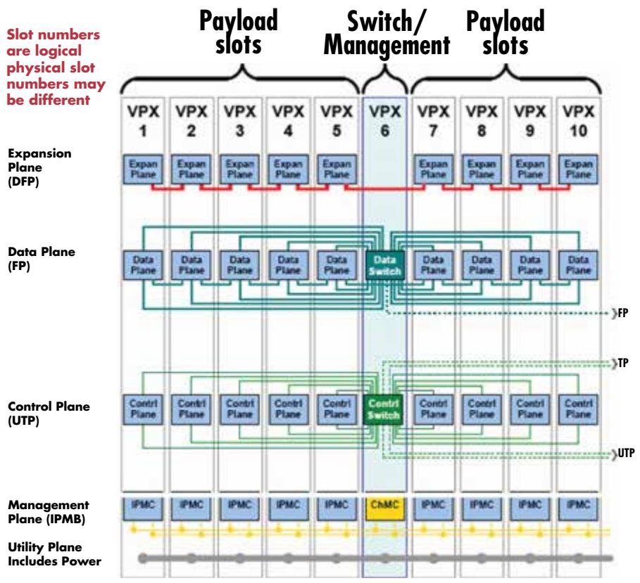
The backplane configuration examples show the connectivity across the backplane for various planes. This includes the routing topology across the data plane and the connections across the expansion, control, management and utility planes. They also provide an illustration of the slot types, whether payload, switch or legacy bus slots.
![Based on the provided image, here is an accurate and concise description of the flowchart, organized by the horizontal planes (rows) from top to bottom:  **Top Grouping** *   **Labels:** 'Payload slots' covers columns 1-5; 'Switch/Management' covers column 6; 'Payload slots' covers columns 7-10. *   **Note:** Red text states, 'Slot numbers are logical physical slot numbers may be different'. *   **Column Headers:** VPX 1, VPX 2, VPX 3, VPX 4, VPX 5, VPX 6, VPX 7, VPX 8, VPX 9, VPX 10.  **1. Expansion Plane (DFP)** *   **Blocks:** Labeled 'Expans Plane' (noting the typo in the image) located in VPX 1, 2, 3, 4, 5, 7, 8, 9, and 10. *   **Connections:** A solid red line connects all 'Expans Plane' blocks horizontally.  **2. Data Plane (FP)** *   **Blocks:** Labeled 'Data Plane' located in VPX 1, 2, 3, 4, 5, 7, 8, 9, and 10. A central block labeled 'Data Switch' is located in VPX 6. *   **Connections:** Green lines connect the 'Data Plane' blocks in columns 1-5 to the 'Data Switch'. Green lines connect the 'Data Plane' blocks in columns 7-10 to the 'Data Switch'. A dotted line extends to the right labeled 'FP'.  **3. Control Plane (UTP)** *   **Blocks:** Labeled 'Contrl Plane' located in VPX 1, 2, 3, 4, 5, 7, 8, 9, and 10. A central block labeled 'Contrl Switch' is located in VPX 6. *   **Connections:** Green lines connect the 'Contrl Plane' blocks in columns 1-5 to the 'Contrl Switch'. Dotted lines connect the 'Contrl Plane' blocks in columns 7-10 to the 'Contrl Switch'. Labels 'TP' and 'UTP' appear on the right edge.  **4. Management Plane (IPMB)** *   **Blocks:** Labeled 'IPMC' located in VPX 1, 2, 3, 4, 5, 7, 8, 9, and 10. A yellow block labeled 'ChMC' is located in VPX 6. *   **Connections:** Yellow dashed lines connect all blocks horizontally.  **5. Utility Plane Includes Power** *   **Connections:** A grey line with dots runs across the bottom of the diagram.](.elma-vpx-backplanes-technical-reference-guide/75c69e976008704ff6df94e21b2a600bca1978633807b063f9b0ecced92738a6.jpg)

# DATA RATES

OpenVPX defines the data rates of each Plane (Control, Data and Expansion) on the Backplane. They begin at 1.25 Gbaud/link and currently exceed 6.25 Gbaud/link.

Note: Gbaud refers to the useful data transmitted per second. Gbps is usually larger and includes additional signals such as parity bits and packet headers.

<table><tr><td rowspan="2">Profile Name</td><td colspan="2">Mechanical</td><td colspan="2">Slot Profiles and Section</td><td>Gbaud Rate</td></tr><tr><td>Pitch (in)</td><td>RTM Conn</td><td>Payload</td><td>Payload or Peripheral</td><td>Data Plane Channel</td></tr><tr><td>BKP3-CEN03-15.2.9-1</td><td>1.0</td><td>VITA 46.10</td><td>SLT3-PAY-2F-14.2.7</td><td>SLT3-PER-1F-14.3.2</td><td>2.5</td></tr><tr><td>BKP3-CEN03-15.2.9-2</td><td>1.0</td><td>VITA 46.10</td><td>SLT3-PAY-2F-14.2.7</td><td>SLT3-PER-1F-14.3.2</td><td>5.0</td></tr><tr><td>BKP3-CEN03-15.2.9-3</td><td>1.0</td><td>VITA 46.10</td><td>SLT3-PAY-2F-14.2.7</td><td>SLT3-PER-1F-14.3.2</td><td>6.25</td></tr><tr><td>BKP3-CEN03-15.2.9-4</td><td>1.0</td><td>VITA 46.10</td><td>SLT3-PAY-2F-14.2.7</td><td>SLT3-PER-1F-14.3.2</td><td>8.0</td></tr></table>

UTILITY SIGNALS

<table><tr><td>J0/P0 Pin/Signal</td><td>Description</td></tr><tr><td>Vs1</td><td>High Voltage Power Input 1 Voltage specified in VITA 65. Capability per VITA 46.0 Table 4-5</td></tr><tr><td>Vs2</td><td>High Voltage Power Input 2 Voltage specified differently for 3U or 6U in VITA 65. Capability per VITA 46.0 Table 4-5</td></tr><tr><td>Vs3</td><td>Low Voltage Power Input 3 Voltage specified in VITA 65. Capability per VITA 46.0 Table 4-5</td></tr><tr><td>GA[4:0]*, GAP*</td><td>Geographical Address Inputs 0-4, Parity. Grounded in each slot per VITA 46.0 Table 7-1.</td></tr><tr><td>SM[3:0]</td><td>System Management connections bussed per Phillips Semiconductor I2C-Bus Specification, Version 2.1, January 2000</td></tr><tr><td>AUX_CLK+/-</td><td>Optional auxiliary reference clock (see ANSI/VITA 65) matched better than 8.5 pS and differentially terminated to 130 Ohms ± 10%.</td></tr><tr><td>3.3V_AUX</td><td>3.3V Auxiliary power, System Management, 1.0 A per slot.</td></tr><tr><td>+/- 12V_AUX</td><td>Auxiliary Power Supplies, 1.0 A per slot.</td></tr><tr><td>SYSRESET*</td><td>System Reset, bussed to all slots &amp; terminated w 5% 220-ohm pull-up resistors to 3.3V AUX &amp; 1.8K-ohm pull-down to GND or equiv.</td></tr><tr><td>REF_CLK+/-</td><td>Reference Clock 25 MHz matched better than 8.5 pS and differentially terminated at each end with a resistor of 61.9 Ohms ± 1%.</td></tr><tr><td>NVMRO</td><td>Non-Volatile Memory Read Only, bussed to all slots and pulled to 3.3V_AUX through 5% 220 ohm resistor</td></tr><tr><td>TCK, TMS, TRST*, TDI, TDO</td><td>JTAG Signals, not bussed or terminated on the backplane.</td></tr><tr><td>No Pad</td><td>The construction of the connector wafer is such that there is no circuit pad in this location</td></tr></table>

<table><tr><td>JJ1/P1 Pin/Signal</td><td>Description</td></tr><tr><td>GDiscrete1</td><td>Optional single ended general purpose I/O signal, bussed to each slot.</td></tr><tr><td>P1-VBAT</td><td>Battery Voltage, Bussed, 3V +/- 15% source on the backplane.</td></tr><tr><td>SYS_CON*</td><td>When grounded the backplane the SYS_CON mode is set. Implemented in by a jumper at any slot to be so designated.</td></tr><tr><td>MaskableReset*</td><td>Optional local reset input to Plug-In Module in addition to global SYSRESET*. Implemented as “opt-in” via jumper at each slot.</td></tr></table>

Table 3.7-2 Utility Plane Signals on J0

<table><tr><td></td><td>Row i</td><td></td><td>Row i</td><td>Row h</td><td>Row g</td><td>Row f</td><td>Row e</td><td>Row d</td><td>Row c</td><td>Row b</td><td>Row a</td></tr><tr><td>1</td><td>GDiscrete1</td><td>1</td><td>Vs1</td><td>Vs1</td><td>Vs1</td><td>Vs1</td><td>No Pad*</td><td>Vs2</td><td>Vs2</td><td>Vs2</td><td>Vs2</td></tr><tr><td>2</td><td>GND</td><td>2</td><td>Vs1</td><td>Vs1</td><td>Vs1</td><td>Vs1</td><td>No Pad*</td><td>Vs2</td><td>Vs2</td><td>Vs2</td><td>Vs2</td></tr><tr><td>3</td><td>P1-VBAT</td><td>3</td><td>Vs3</td><td>Vs3</td><td>Vs3</td><td>Vs3</td><td>No Pad*</td><td>Vs3</td><td>Vs3</td><td>Vs3</td><td>Vs3</td></tr><tr><td>4</td><td>GND</td><td>4</td><td>GND</td><td>SM2</td><td>SM3</td><td>GND</td><td>-12V_Aux</td><td>GND</td><td>SYSRESET*</td><td>NVMRO</td><td>GND</td></tr><tr><td>5</td><td>SYS_CON*</td><td>5</td><td>GND</td><td>GAP*</td><td>GA4*</td><td>GND</td><td>3.3V_Aux</td><td>GND</td><td>SM0</td><td>SM1</td><td>GND</td></tr><tr><td>6</td><td>GND</td><td>6</td><td>GND</td><td>GA3*</td><td>GA2*</td><td>GND</td><td>+12V_Aux</td><td>GND</td><td>GA1*</td><td>GA0*</td><td>GND</td></tr><tr><td>7</td><td>Reserved</td><td>7</td><td>TCK</td><td>GND</td><td>GND</td><td>TDO</td><td>TDI</td><td>GND</td><td>GND</td><td>TMS</td><td>TRST*</td></tr><tr><td>8</td><td>GND</td><td rowspan="2">8</td><td rowspan="2">GND</td><td rowspan="2">REF_CLK-</td><td rowspan="2">REF_CLK+</td><td rowspan="2">GND</td><td rowspan="2">GND</td><td rowspan="2">AUX_CLK-</td><td rowspan="2">AUX_CLK+</td><td rowspan="2">GND</td><td rowspan="2">GND</td></tr><tr><td>9</td><td>UD</td></tr><tr><td>10</td><td>GND</td><td rowspan="7" colspan="9">← UD pins in Row i can be assigned by Slot Profiles in Sections 10 and 14.The pairs on Rows a thru h are assigned by Slot Profiles in Sections 10 and 14.</td><td rowspan="7"></td></tr><tr><td>11</td><td>UD</td></tr><tr><td>12</td><td>GND</td></tr><tr><td>13</td><td>UD</td></tr><tr><td>14</td><td>GND</td></tr><tr><td>15</td><td>MaskableReset*</td></tr><tr><td>16</td><td>GND</td></tr></table>

Table 3.7-4 Utility Plane Signals on J1

# BACKPLANE AND DAUGHTER CARD PINOUT CHART

This chart shows the specification pinout of both the backplane and daughter card for J2-J6. Note the differences between the plug-in module and the backplane (even and odd pins) for Row E and Row B. Although the number of rows is different, the connector arrangement allows single-ended signals in these areas. The backplane and daugther card connectors mate without issue.

<table><tr><td rowspan="2"></td><td rowspan="2">Row G</td><td rowspan="2">Row F</td><td colspan="2">Row E</td><td rowspan="2">Row D</td><td rowspan="2">Row C</td><td colspan="2">Row B</td><td rowspan="2">Row A</td></tr><tr><td>Even</td><td>Odd</td><td>Even</td><td>Odd</td></tr><tr><td>Back-plane J2-J6</td><td>Row i</td><td>Row h</td><td>Row g</td><td>Row f</td><td>Row e</td><td>Row d</td><td>Row c</td><td>Row b</td><td>Row a</td></tr><tr><td>1</td><td>SEwafer1</td><td>GND</td><td>GND-J2</td><td>LN0-TD-</td><td>LN0-TD+</td><td>GND</td><td>GND-J2</td><td>LN0-RD-</td><td>LN0-RD+</td></tr><tr><td>2</td><td>GND</td><td>LN1-TD-</td><td>LN1-TD+</td><td>GND-J2</td><td>GND</td><td>LN1-RD-</td><td>LN1-RD+</td><td>GND-J2</td><td>GND</td></tr><tr><td>3</td><td>SEwafer3</td><td>GND</td><td>GND-J2</td><td>LN2-TD-</td><td>LN2-TD+</td><td>GND</td><td>GND-J2</td><td>LN2-RD-</td><td>LN2-RD+</td></tr><tr><td>4</td><td>GND</td><td>LN3-TD-</td><td>LN3-TD+</td><td>GND-J2</td><td>GND</td><td>LN3-RD-</td><td>LN3-RD+</td><td>GND-J2</td><td>GND</td></tr><tr><td>5</td><td>SEwafer5</td><td>GND</td><td>GND-J2</td><td>LN4-TD-</td><td>LN4-TD+</td><td>GND</td><td>GND-J2</td><td>LN4-RD-</td><td>LN4-RD+</td></tr><tr><td>6</td><td>GND</td><td>LN5-TD-</td><td>LN5-TD+</td><td>GND-J2</td><td>GND</td><td>LN5-RD-</td><td>LN5-RD+</td><td>GND-J2</td><td>GND</td></tr><tr><td>7</td><td>SEwafer7</td><td>GND</td><td>GND-J2</td><td>LN6-TD-</td><td>LN6-TD+</td><td>GND</td><td>GND-J2</td><td>LN6-RD-</td><td>LN6-RD+</td></tr><tr><td>8</td><td>GND</td><td>LN7-TD-</td><td>LN7-TD+</td><td>GND-J2</td><td>GND</td><td>LN7-RD-</td><td>LN7-RD+</td><td>GND-J2</td><td>GND</td></tr><tr><td>9</td><td>SEwafer9</td><td>GND</td><td>GND-J2</td><td>LN8-TD-</td><td>LN8-TD+</td><td>GND</td><td>GND-J2</td><td>LN8-RD-</td><td>LN8-RD+</td></tr><tr><td>10</td><td>GND</td><td>LN9-TD-</td><td>LN9-TD+</td><td>GND-J2</td><td>GND</td><td>LN9-RD-</td><td>LN9-RD+</td><td>GND-J2</td><td>GND</td></tr><tr><td>11</td><td>SEwafer11</td><td>GND</td><td>GND-J2</td><td>LN10-TD-</td><td>LN10-TD+</td><td>GND</td><td>GND-J2</td><td>LN10-RD-</td><td>LN10-RD+</td></tr><tr><td>12</td><td>GND</td><td>LN11-TD-</td><td>LN11-TD+</td><td>GND-J2</td><td>GND</td><td>LN11-RD-</td><td>LN11-RD+</td><td>GND-J2</td><td>GND</td></tr><tr><td>13</td><td>SEwafer13</td><td>GND</td><td>GND-J2</td><td>LN12-TD-</td><td>LN12-TD+</td><td>GND</td><td>GND-J2</td><td>LN12-RD-</td><td>LN12-RD+</td></tr><tr><td>14</td><td>GND</td><td>LN13-TD-</td><td>LN13-TD+</td><td>GND-J2</td><td>GND</td><td>LN13-RD-</td><td>LN13-RD+</td><td>GND-J2</td><td>GND</td></tr><tr><td>15</td><td>SEwafer15</td><td>GND</td><td>GND-J2</td><td>LN14-TD-</td><td>LN14-TD+</td><td>GND</td><td>GND-J2</td><td>LN14-RD-</td><td>LN14-RD+</td></tr><tr><td>16</td><td>GND</td><td>LN15-TD-</td><td>LN15-TD+</td><td>GND-J2</td><td>GND</td><td>LN15-RD-</td><td>LN15-RD+</td><td>GND-J2</td><td>GND</td></tr></table>

# VPX CONNECTOR

![Close-up of a green, grid-patterned electronic device with black components on a green circuit board (no visible text or symbols)](.elma-vpx-backplanes-technical-reference-guide/f83602ba8c44af3e35efdcf7ad5d924b399f1c109af7e6b326cc474aaf5527f3.jpg)

![The image displays a diagram featuring four vertical columns of rectangular blocks, accompanied by text and arrows.  From left to right, the columns are: 1.  A column alternating between red and yellow blocks. 2.  A column of green blocks separated by thin red vertical lines. 3.  A column alternating between yellow and red blocks, starting with a yellow block at the top. 4.  A column of green blocks separated by thin red vertical lines.  Two red arrows point downwards towards the columns: *   The left arrow is labeled 'Every Row' and points towards the leftmost column. *   The right arrow is labeled 'Odd Row' and points towards the top yellow block of the third column.](.elma-vpx-backplanes-technical-reference-guide/506fe693af0af134350d070f74596c551d64ee8cb97c8eb5bc7d597cabd1ee40.jpg)

With the exception of J0 rows 1-6, OpenVPX daughter card connectors are constructed of alternating even and odd wafer elements. As a result of this design, the odd wafer rows have a SE pin in daughter card column “g” that corresponds to backplane wafer column “i”.

Elma can provide backplanes with either TE MultiGig™ or EPT Velox™ connectors in accordance with ANSI-VITA 46. The EPT Velox™ is Standard on Elma VPX development backplanes. Backplanes can also be assembled with backplane connectors in accordance with ANSI VITA 60 or 63 connectors or a combination of slots fitted with VITA 46, 60 or 63 connectors as they are all footprint compatible, though not intermateable.

# CHARACTERISTICS

![Two electronic components: a green heat sink and a grid-patterned base (no visible text or symbols)](.elma-vpx-backplanes-technical-reference-guide/9df7f6af0340f9d986f29153dac56e856bbf1eae6a240bc3f3e4523f2c99a26c.jpg)

<table><tr><td>Operating Voltage:</td><td>50 Volts AC peak or DC</td></tr><tr><td>Current:</td><td>1 amp at &lt;30°C (single circuit, free air)</td></tr><tr><td>Temperature:</td><td>-55°C to 105°C</td></tr><tr><td>Insulation resistance:</td><td>1000 megohms minimum</td></tr><tr><td>Temperature rise vs. current:</td><td>30°C maximum temperature at 1 amp load,</td></tr></table>

# ODD AND EVEN WAFER DESIGN

![Based on the provided flowchart/block diagram, here are the labeled blocks and connections:  **Labeled Blocks and Contents:**  *   **Backplane PWB**: A vertical block on the left containing rows labeled **a** through **i**.     *   Rows **a**, **b**, **e**, **f**, and **i** are labeled **GND**.     *   Row **c** is labeled **cx**.     *   Row **d** is labeled **dx**.     *   Row **g** is labeled **gx**.     *   Row **h** is labeled **hx**. *   **Connector Wafer**: A large central block containing rows labeled **ax** through **ix**.     *   Rows **ax**, **bx**, **ex**, **fx**, and **ix** are labeled **GND**.     *   Rows **cx**, **dx**, **gx**, and **hx** retain their labels (**cx**, **dx**, **gx**, **hx**).     *   The block contains text labels **Pair 1** and **Pair 2**. *   **Plug-in Module PWB**: A block at the bottom containing a sub-block labeled **Plug-in Row**.     *   The row contains pins labeled **A**, **B**, **C**, **D**, **E**, **F**, and **G**.     *   There are connection labels **to cx**, **to dx**, **to gx**, and **to hx**.  **Connections:**  Blue lines connect the components as follows:  *   **Pair 1**: Connects pins **c** (**cx**) and **d** (**dx**) from the **Backplane PWB** to the corresponding pins **cx** and **dx** in the **Connector Wafer**. From there, lines labeled **to cx** and **to dx** connect to pins **B** and **C** on the **Plug-in Module PWB**, respectively. *   **Pair 2**: Connects pins **g** (**gx**) and **h** (**hx**) from the **Backplane PWB** to the corresponding pins **gx** and **hx** in the **Connector Wafer**. From there, lines labeled **to gx** and **to hx** connect to pins **F** and **G** on the **Plug-in Module PWB**, respectively.](.elma-vpx-backplanes-technical-reference-guide/a0c6f4e9ed4da06f4e2584e46d558d337da3b0ce41968984075441d43af0050a.jpg)

VITA 46 Wafer - Even Differential Pair

![The image displays a block diagram illustrating signal connections between three main components:  **1. Backplane PWB (Left Block)** *   A vertical rectangular block labeled **'Backplane PWB'**. *   Inside is a column labeled **'Backplane Row'**. *   The rows contain the following text (from top to bottom):     *   **'i ix'**     *   **'h GND'**     *   **'g GND'**     *   **'f fx'**     *   **'e ex'**     *   **'d GND'**     *   **'c GND'**     *   **'a ax'**  **2. Connector Wafer (Center Block)** *   A large rectangular block labeled **'Connector Wafer'**. *   Inside is a column of labels (from top to bottom):     *   **'ix'**     *   **'hx'**     *   **'GND'**     *   **'gx'**     *   **'fx'**     *   **'ex'**     *   **'dx'**     *   **'cx'**     *   **'bx'**     *   **'ax'**  **3. Plug-in Module PWB (Right/Bottom Block)** *   A horizontal rectangular block labeled **'Plug-in Module PWB'**. *   Inside is a row labeled **'Plug-in Row'**. *   The cells contain the following labels (from left to right):     *   **'A'**     *   **'B'**     *   **'C'**     *   **'D'**     *   **'E'**     *   **'F'**     *   **'G'**  **Connections** *   Thick blue paths connect the labeled rows in the **'Connector Wafer'** to the cells in the **'Plug-in Row'**. *   The paths are nested like a rainbow. *   Specific paths are labeled:     *   **'Single Ended 1'** is next to the outermost path starting at **'ix'**.     *   **'Pair 2'** is next to the paths starting at **'fx'** and **'ex'**.     *   **'Pair 1'** is next to the innermost paths starting at **'bx'** and **'ax'**. *   The paths end at the columns labeled **'A'** through **'G'** in the Plug-in Row.](.elma-vpx-backplanes-technical-reference-guide/a3897c460a91457d4d8ffb4e75c1df6d5eab2abd6ec04bc78ca2462bd09f2198.jpg)

VITA 46 Wafer - Odd Differential Pair

# IPMB CONNECTOR (SMT)

![This image features a cream-colored plastic electrical connector, likely a PCB header. It consists of a long rectangular housing with vertical dividers creating a row of slots for contacts, extending into a shorter, perpendicular section with two distinct cavities. Silver metal pins protrude from the bottom edge for through-hole mounting. No text is visible on the component.](.elma-vpx-backplanes-technical-reference-guide/3c6d7abfd28e7ccff85d7684b174982d3a473c157b629dd77c4be9d511e5cec1.jpg)

![The image shows a close-up, slightly blurry view of a green printed circuit board. At the very top, a golden, out-of-focus object is visible above a large, black rectangular component featuring a grid-like pattern, likely a socket. Below this, two white rectangular connectors, resembling DIP switches or headers, are mounted on the board with small metal pins visible on their tops. To the right of these switches, small yellow pins are arranged in rows on the green circuit board surface. There is no legible text in the image.](.elma-vpx-backplanes-technical-reference-guide/22cabadffc00940097128797bb5548a72722d182899d9d2d6d5908b50b6bdc5a.jpg)

<table><tr><td>Number of Positions:</td><td>5</td></tr><tr><td>Number of Rows:</td><td>1</td></tr><tr><td>Operating Temperature:</td><td>85.0°C (max)</td></tr><tr><td>Contact Material:</td><td>Phosphor Bronze</td></tr><tr><td>Flammability Rating:</td><td>UL 94 V-0</td></tr><tr><td>Gender:</td><td>Male</td></tr><tr><td>Current Rating:</td><td>1.3A at @ 30°C rise</td></tr><tr><td>Mfg Part Number:</td><td>Molex PicoBlade(tm) 53398-0571</td></tr></table>

# KEYING GUIDE

VPX alignment and module keying is accomplished by the use of pins on the backplane and sockets on the daughter card. The pins have a flat side that can be oriented in five different positions: 0, 45, 90, 270 or 315 degrees. In standard development backplanes, each slot has a unique key combination.

The chart below gives the recommended keying arrangement for 3U or 6U backplanes. Additionally, the key receptacle on the daughter card has electrical contacts so that the keying is part of the VPX safety ground system. The backplane key orientation can be changed by the user, and a daughter card receptacle key can be a full circle without a flat, which allows a daughter card to be placed over backplane keys of any orientation. Double-ended backplane guide modules provide RTM keying and alignment.

<table><tr><td>Backplane Slot*</td><td>Voltage Key Position 1</td><td>Key Position 2</td><td>Key Position 3</td></tr><tr><td>Slot 1</td><td>315</td><td>270</td><td>270</td></tr><tr><td>Slot 2</td><td>315</td><td>315</td><td>270</td></tr><tr><td>Slot 3</td><td>315</td><td>0</td><td>270</td></tr><tr><td>Slot 4</td><td>315</td><td>45</td><td>270</td></tr><tr><td>Slot 5</td><td>315</td><td>90</td><td>270</td></tr><tr><td>Slot 6</td><td>315</td><td>270</td><td>315</td></tr><tr><td>Slot 7</td><td>315</td><td>315</td><td>315</td></tr><tr><td>Slot 8</td><td>315</td><td>0</td><td>315</td></tr><tr><td>Slot 9</td><td>315</td><td>45</td><td>315</td></tr><tr><td>Slot 10</td><td>315</td><td>90</td><td>315</td></tr><tr><td>Slot 11</td><td>315</td><td>270</td><td>0</td></tr><tr><td>Slot 12</td><td>315</td><td>315</td><td>0</td></tr><tr><td>Slot 13</td><td>315</td><td>0</td><td>0</td></tr><tr><td>Slot 14</td><td>315</td><td>45</td><td>0</td></tr><tr><td>Slot 15</td><td>315</td><td>90</td><td>0</td></tr><tr><td>Slot 16</td><td>315</td><td>270</td><td>45</td></tr><tr><td>Slot 17</td><td>315</td><td>315</td><td>45</td></tr><tr><td>Slot 18</td><td>315</td><td>0</td><td>45</td></tr><tr><td>Slot 19</td><td>315</td><td>45</td><td>45</td></tr><tr><td>Slot 20</td><td>315</td><td>90</td><td>45</td></tr><tr><td>Slot 21</td><td>315</td><td>270</td><td>90</td></tr><tr><td>Slot 22</td><td>315</td><td>315</td><td>90</td></tr><tr><td colspan="2"></td><td>Backplane</td><td>FTM RTM</td></tr><tr><td colspan="2">Front Module</td><td>1469491-C</td><td>1469492-C</td></tr><tr><td colspan="2">Front Rear Double Key*</td><td>1410956-C</td><td>1469492-C</td></tr><tr><td colspan="4">* Double ended for backplane. FTM and RTM use same</td></tr></table>

![Metal keying pin component with threaded tip and threaded base (no text or symbols on the pin itself)](.elma-vpx-backplanes-technical-reference-guide/1d6d550b2f4be2950eb102c92314623b048b9c6f7802511534f41afbaffaa7a3.jpg)

![Close-up of a mechanical component with ribbed internal structure, labeled 'Keying Guide' (no other text or symbols visible)](.elma-vpx-backplanes-technical-reference-guide/e1fc3bf5233b545b680f4752be1c159359e7770278a3f594bb732c0cab179038.jpg)

![Double-Ended Guide](.elma-vpx-backplanes-technical-reference-guide/690adcf6129e823af69b70e5d7903155cdcb01d04bee8a9e760c91c2e6e321f9.jpg)

# VPX - AVAILABLE POWER & VOLTAGE ASSIGNMENTS

The chart below gives maximum power per VPX slot based upon VITA 46 and profiles defined in VITA 65.

<table><tr><td>Voltage Level</td><td>3U watts/slot</td><td>6U watts/slot</td><td>per wafer due to connector limits</td></tr><tr><td>Only 3V</td><td>69</td><td>N/A</td><td>23 Amps†</td></tr><tr><td>Only 5V</td><td>115</td><td>115</td><td>23 Amps†</td></tr><tr><td>Only 12V*</td><td>276</td><td>384</td><td>23 Amps† (3U), 16 Amps‡ (6U)</td></tr><tr><td>VS1, VS2, and VS3</td><td>240</td><td>348</td><td>12 Amps§</td></tr><tr><td>Only 48v per VITA 46</td><td>N/A</td><td>768</td><td>16 Amps‡ (VS1 and VS2)</td></tr></table>

Note: †= 1 power wafer used, ‡=2 power wafers used, §=3 power wafers used

The assignment of voltages on VS1, VS2 and VS3 is different for 3U and 6U cards. In addition, more voltage options are alowed for VS1 and VS2 in VITA 46 than are currently defined within VITA 65.

# SIGNAL ASSIGNMENTS FOR THE J0 CONNECTOR PER VITA 46.0 AND VITA 65

<table><tr><td></td><td>Row i</td><td>Row h</td><td>Row g</td><td>Row f</td><td>Row e</td><td>Row d</td><td>Row c</td><td>Row b</td><td>Row a</td></tr><tr><td>1</td><td>Vs1</td><td>Vs1</td><td>Vs1</td><td>Vs1</td><td>No Pad*</td><td>Vs2</td><td>Vs2</td><td>Vs2</td><td>Vs2</td></tr><tr><td>2</td><td>Vs1</td><td>Vs1</td><td>Vs1</td><td>Vs1</td><td>No Pad*</td><td>Vs2</td><td>Vs2</td><td>Vs2</td><td>Vs2</td></tr><tr><td>3</td><td>Vs3</td><td>Vs3</td><td>Vs3</td><td>Vs3</td><td>No Pad*</td><td>Vs3</td><td>Vs3</td><td>Vs3</td><td>Vs3</td></tr><tr><td>4</td><td>GND</td><td>SM2</td><td>SM3</td><td>GND</td><td>-12V_Aux</td><td>GND</td><td>SYSRESET*</td><td>NVMRO</td><td>GND</td></tr><tr><td>5</td><td>GND</td><td>GAP*</td><td>GA4*</td><td>GND</td><td>3.3V_Aux</td><td>GND</td><td>SM0</td><td>SM1</td><td>GND</td></tr><tr><td>6</td><td>GND</td><td>GA3*</td><td>GA2*</td><td>GND</td><td>+12V_Aux</td><td>GND</td><td>GA1*</td><td>GA0*</td><td>GND</td></tr><tr><td>7</td><td>TCK</td><td>GND</td><td>GND</td><td>TDO</td><td>TDI</td><td>GND</td><td>GND</td><td>TMS</td><td>TRST*</td></tr><tr><td>8</td><td>GND</td><td>REF_CLK-</td><td>REF_CLK*</td><td>GND</td><td>GND</td><td>AUX_CLK-</td><td>AUX_CLK*</td><td>GND</td><td>GND</td></tr></table>

# 3U POWER ASSIGNMENTS FOR THE J0 CONNECTOR PER VITA 65

<table><tr><td></td><td>Row i</td><td>Row h</td><td>Row g</td><td>Row f</td><td>Row e</td><td>Row d</td><td>Row c</td><td>Row b</td><td>Row a</td></tr><tr><td>1</td><td>12V</td><td>12V</td><td>12V</td><td>12V</td><td>No Pad*</td><td>3V</td><td>3V</td><td>3V</td><td>3V</td></tr><tr><td>2</td><td>12V</td><td>12V</td><td>12V</td><td>12V</td><td>No Pad*</td><td>3V</td><td>3V</td><td>3V</td><td>3V</td></tr><tr><td>3</td><td>5V</td><td>5V</td><td>5V</td><td>5V</td><td>No Pad*</td><td>5V</td><td>5V</td><td>5V</td><td>5V</td></tr><tr><td>4</td><td>GND</td><td>SM2</td><td>SM3</td><td>GND</td><td>-12V_Aux</td><td>GND</td><td>SYSRESET*</td><td>NVMRO</td><td>GND</td></tr><tr><td>5</td><td>GND</td><td>GAP*</td><td>GA4*</td><td>GND</td><td>3.3V_Aux</td><td>GND</td><td>SM0</td><td>SM1</td><td>GND</td></tr><tr><td>6</td><td>GND</td><td>GA3*</td><td>GA2*</td><td>GND</td><td>+12V_Aux</td><td>GND</td><td>GA1*</td><td>GA0*</td><td>GND</td></tr><tr><td>7</td><td>TCK</td><td>GND</td><td>GND</td><td>TDO</td><td>TDI</td><td>GND</td><td>GND</td><td>TMS</td><td>TRST*</td></tr><tr><td>8</td><td>GND</td><td>REF_CLK-</td><td>REF_CLK+</td><td>GND</td><td>GND</td><td>AUX_CLK-</td><td>AUX_CLK+</td><td>GND</td><td>GND</td></tr></table>

# 6U POWER ASSIGNMENTS FOR THE J0 CONNECTOR PER VITA 65

<table><tr><td></td><td>Row i</td><td>Row h</td><td>Row g</td><td>Row f</td><td>Row e</td><td>Row d</td><td>Row c</td><td>Row b</td><td>Row a</td></tr><tr><td>1</td><td>12V</td><td>12V</td><td>12V</td><td>12V</td><td>No Pad*</td><td>12V</td><td>12V</td><td>12V</td><td>12V</td></tr><tr><td>2</td><td>12V</td><td>12V</td><td>12V</td><td>12V</td><td>No Pad*</td><td>12V</td><td>12V</td><td>12V</td><td>12V</td></tr><tr><td>3</td><td>5V</td><td>5V</td><td>5V</td><td>5V</td><td>No Pad*</td><td>5V</td><td>5V</td><td>5V</td><td>5V</td></tr><tr><td>4</td><td>GND</td><td>SM2</td><td>SM3</td><td>GND</td><td>-12V_Aux</td><td>GND</td><td>SYSRESET*</td><td>NVMRO</td><td>GND</td></tr><tr><td>5</td><td>GND</td><td>GAP*</td><td>GA4*</td><td>GND</td><td>3.3V_Aux</td><td>GND</td><td>SM0</td><td>SM1</td><td>GND</td></tr><tr><td>6</td><td>GND</td><td>GA3*</td><td>GA2*</td><td>GND</td><td>+12V_Aux</td><td>GND</td><td>GA1*</td><td>GA0*</td><td>GND</td></tr><tr><td>7</td><td>TCK</td><td>GND</td><td>GND</td><td>TDO</td><td>TDI</td><td>GND</td><td>GND</td><td>TMS</td><td>TRST*</td></tr><tr><td>8</td><td>GND</td><td>REF_CLK-</td><td>REF_CLK+</td><td>GND</td><td>GND</td><td>AUX_CLK-</td><td>AUX_CLK+</td><td>GND</td><td>GND</td></tr></table>

# VPX SIGNAL INTEGRITY CONSIDERATIONS

With VPX backplanes pushing the speed envelope, every feature of the design can influence signal integrity – every trace, layer separation, turn bend, via, via transition, etc. Elma’s signal integrity analysis and simulations look at the entire channel in order to ensure optimal performance.

Our simulation is very detailed, looking closely at each element in the channel. We focus on each of the various structures and launches, along with lossy trace models, to model the complete channel as accurately as possible. By focusing on each structure individually, we can optimize the return loss for each. Once the structures are modeled, they are concatenated together along with the lossy trace models and connector models to create the complete channel. When there are four complete coupled channels modeled - 2 TX and 2 RX - we utilize a connector model that also has four pairs. Transmission lines are created in W-element tabular format using RLGC, a 2D Field Solver. The fitted

![  Parameter   Value         ---------   ---------     ehpk        278.4mV       ehc         271.6mV       oeh         557.4mV       ew          0.607UI       ewoff       0.022UI       ehoff       0.015UI       lanes        3             nui         80            cb          6             v0.54       -          ](.elma-vpx-backplanes-technical-reference-guide/19a4d2373578cadcfb26d49f6eba13d16a27a8e05d57c1dd68933898d1ab9861.jpg)

attenuation, IL, ILD, RL and ICR will be compared to the channel requirements. We use symmetry and algebraically add noise components to account for the total noise in the system. This total noise includes the coupled noise generated in the connector via fields as well as the connectors themselves.

We generate S-parameter models and run the simulation in Ansoft HFSS. For instance, when dealing with a typically thick 30-layer N4000-13EPSI backplane design, we need to ensure compliance to the stringent 10 Gbps KR frequency domain requirements. For each simulation, four complete channels (2-TX and 2-RX) are modeled. These channels are coupled together in the connector via footprints as well as the connector models to account for the total noise generated. We start by modeling the worst-case channel parameters. This would include a channel being routed on the lowest backplane layer (L28) in the stack. We will use the largest multilane connector model available. For PCIe Gen3 analysis, SEASIM is the preferred tool for channel performance. If problems are encountered, specific recommendations for resolving those problems are recommended and verified via additional simulation.

# QUALITY BEGINS & ENDS WITH THE CUSTOMER

This is reflected throughout Elma. Our quality procedures meet ISO 9001 & AS9100C standards, ensuring that we meet the most rigorous requirements.

![Three electronic equipment units: a green server tower, a green circuit board with multiple ports, and a beige control unit (no visible text or symbols)](.elma-vpx-backplanes-technical-reference-guide/ad8c868f1a5bc98a54147ff820be214ab4698f4957467398c4e1ac2fc069dcb0.jpg)

![  Country   Marker    --------- --------    North America   Square marker (orange)     Europe   Square marker (orange)     Asia   Square marker (orange)     Australia   Square marker (orange)     Africa   Square marker (orange)     South America   Square marker (orange)     Middle East   Square marker (orange)     Central Asia   Square marker (orange)     Russia   Square marker (orange)     Canada   Square marker (orange)     Mexico   Square marker (orange)     Brazil   Square marker (orange)     Argentina   Square marker (orange)     United States   Square marker (orange)     China   Square marker (orange)     India   Square marker (orange)     Japan   Square marker (orange)     Germany   Square marker (orange)     France   Square marker (orange)     Italy   Square marker (orange)     Spain   Square marker (orange)     Netherlands   Square marker (orange)     Sweden   Square marker (orange)     Norway   Square marker (orange)     Denmark   Square marker (orange)     Finland   Square marker (orange)     Austria   Square marker (orange)     Switzerland   Square marker (orange)     Belgium   Square marker (orange)     United Kingdom   Square marker (orange)     Israel   Square marker (orange)     Iran   Square marker (orange)     Saudi Arabia   Square marker (orange)     Kuwait   Square marker (orange)     Bahrain   Square marker (orange)     Qatar   Square marker (orange)     Oman   Square marker (orange)     Lebanon   Square marker (orange)     Jordan   Square marker (orange)     Kyrgyzstan   Square marker (orange)     Mongolia   Square marker (orange)     Kazakhstan   Square marker (orange)     Uzbekistan   Square marker (orange)     Turkmenistan   Square marker (orange)     Ecuador   Square marker (orange)     Bolivia   Square marker (orange)     Iceland   Square marker (orange)     Greenland   Square marker (orange)     Antarctica   Square markers (white)  ](.elma-vpx-backplanes-technical-reference-guide/fddbf8604fdcfda3c82b7498882193ba5230a10ebbe33e9adf7b888d78d30365.jpg)

# Elma Electronic Inc. USA

44350 Grimmer Blvd.

Fremont, CA 94538

P: +1 510 656 3400

F: +1 510 656 3783

sales@elma.com

# Optima Stantron

1775 MacLeod Drive

Lawrenceville, GA 30043

P: +1 770 496 4000

F: +1 770 496 4026

sales@optimastantron.com

# Elma Electronic AG, Switzerland

Hofstrasse 93

CH-8620 Wetzikon

P: +41 44 933 41 11

F: +41 44 933 42 15

info@elma.ch

# Elma Electronic GmbH, Germany

Stuttgarter Straße 11

D-75179 Pforzheim

P: +49 7231 97 34 0

F: +49 7231 97 34 97

info@elma.de

# Elma Electronic UK Ltd.

Solutions House, Fraser Road

Priory Business Park

Bedford MK44 3BF, UK

P: +44 1234 838 822

F: +44 1234 836 650

sales@elma.co.uk

If you are using a satellite navigation device

or internet map to find us, please use the

postcode of our neighbours: MK44 3WH

# Elma Electronic France SA

ZA du Buisson Rond

F-38460 Villemoirieu

P: +33 437 06 21 10

F: +33 437 06 21 19

sales@elma-electronic.fr

# Elma Electronic Israel Ltd.

34, Modi’in St.

I.Z. Sgula

Petach Tikva 49271

P: +972 3 930 50 25

F: +972 3 931 31 34

sales@elma.co.il

# Elma Electronic Technology

(Shanghai) Co., Ltd.

Building#11, No.198

Chang Jian Road

Bao Shan District

Shanghai, PRC, 200949

P: +86 21 5866 5908

F: +86 21 5866 5918

sales@elmachina.com

# Elma Asia Pacific Pte. Ltd.

115-A Commonwealth Drive

#03-14 Tanglin Halt Industrial Estate

Singapore 149596

P: +65 6479 8552

F: +65 6479 8662

sales.elmaap@elma.com.sg

# YOUR LOCAL SOLUTION PARTNER
[🔗 Link to the original document](.elma-vpx-backplanes-technical-reference-guide/elma-vpx-backplanes-technical-reference-guide.pdf)
