# Smart Mobility ARChitecture

# Hardware Specification

![Abstract green geometric shape resembling a stylized clover or cross (no text or symbols)](.smarc-hardware-specification-v1-1/6d16d2ac09d8ead4233ebc97d27dd6e37127da94f6593c59770f20eb11de1171.jpg)

# SMARC

Version 1.1 May 29, 2014

© Copyright 2014, SGeT Standardization Group for Embedded Technology e.V.

Note that some content of this SGeT document may be legally protected by patent rights not held by SGeT. SGeT is not obligated to identify the parts of this specification that require licensing or other legitimization. The contents of this SGeT document are advisory only. Users of SGeT documents are responsible for protecting themselves against liability for infringement of patents. All content and information within this document are subject to change without prior notice.

SGeT provides no warranty with regard to this SGeT document or any other information contained herein and hereby expressly disclaims any implied warranties of merchantability or fitness for any particular purpose with regard to any of the foregoing. SGeT assumes no liability for any damages incurred directly or indirectly from any technical or typographical errors or omissions contained herein or for discrepancies between the product and this SGeT document. In no event shall SGeT be liable for any incidental, consequential, special, or exemplary damages, whether based on tort, contract or otherwise, arising out of or in connection with this SGeT document or any other information contained herein or the use thereof.

REVISION HISTORY

<table><tr><td>Rev</td><td>Date</td><td>Originator</td><td>Notes</td></tr><tr><td>1.0</td><td>Dec. 20, 2012</td><td>S.Milnor / Kontron</td><td>Initial release</td></tr><tr><td>1.1</td><td>May 29, 2014</td><td>S.Milnor / Kontron</td><td>Change notes for V1.0 to V1.1 are at the end of this document</td></tr></table>

# TABLE OF CONTENTS

# Introduction ..

1.1 General Introduction......
1.2 SMARC vs. COM Express..
1.3 Purpose of This Document .
1.4 Document and Standards References ... . 8

# 2 Module Overview...... .. 10

2.1 Form Factor Feature Summary.. . 10
2.2 Module Interface Summary.. 11
2.3 Pin Group Summary... . 15

# 3 Module Interface Required and Optional Features... .. 16

3.1 Required and Optional Feature Table..... .... 16
3.2 Feature Fill Order .. . 18

# 4 Signal Descriptions ..... . 19

4.1 Signal Direction and Type Definitions .. . 19
4.2 Display Interfaces.. . 20

4.2.1 Primary Display – 18 / 24 bit Parallel LCD Data . .. 20
4.2.2 Primary LCD Display Support Signals. .. 20
4.2.3 Primary Display – 18 / 24 Bit LVDS LCD Single Channel .. .. 21
4.2.4 Carrier Board Dual Channel LVDS Support.. .. 21
4.2.5 eDP / LVDS LCD Pin Sharing ..... . 22
4.2.6 Secondary (HDMI) Display.. . 23
4.2.7 DP Operation Over HDMI . . 24

# 4.3 Camera Interfaces..... . 25

4.3.1 Camera Configurations... . 25
4.3.2 Module Camera Type Pins.. . 25
4.3.3 Camera Power Enables and Resets . .. 26
4.3.4 Camera I2C Support.. . 27
4.3.5 Serial Camera In - CSI0...... ..... 27
4.3.6 Serial Camera In – CSI1. . 27
4.3.7 Parallel Camera Input – Low Order 10 Bits .... .. 28
4.3.8 Parallel Camera Input – High Order 6 Bits.. . 28
4.3.9 Parallel Camera Input – 2nd Pixel Clock... .. 28

# 4.4 SDIO / SDMMC Interfaces.. . 29

4.4.1 SDIO Card (4 bit) Interface ...... .. 29
4.4.2 eMMC (8 bit) Interface . . 29

# 4.5 SPI Interfaces . . 30

4.5.1 SPI0. . 30
4.5.2 SPI1 .. ... 30

# 4.6 I2S Interfaces. .. 31

4.7 HDA Interface ... .. 31
4.8 SPDIF ... . 32
4.9 I2C Interfaces.. . 32
4.10 Asynchronous Serial Ports ...... . 33
4.11 CAN Bus.. . 34

4.11.1 CAN0 Data. . 34
4.11.2 CAN1 Data ...... .. 34
4.11.3 CAN Bus Error Signals .. . 34

# 4.12 USB Interfaces.. .. 35

4.12.1 USB0... .. 35
4.12.2 USB1... .. 35
4.12.3 USB2... .. 36
4.12.4 USBx\_EN\_OC# Discussion . . 37

# 4.13 PCI Express ..... .. 38

4.13.1 PCIe\_Link A .. . 38

4.13.2 PCIe\_Link B . . 38
4.13.3 PCIe\_Link C. . 39
4.13.4 PCIe Wake.... . 39

4.14 SATA . . 39

4.15 GBE.. . 40
4.16 Watchdog.... . 40
4.17 GPIO... .. 41
4.18 Management Pins . . 42
4.19 Boot Select.. .. 44
4.20 Alternate Function Block.. . 45
4.21 IO Levels..... . 47

4.21.1 Default I/O 1.8V .. . 47
4.21.2 Signals At 3.3V.. . 47
4.21.3 Signals At 5V.. . 47
4.21.4 Deprecation From Spec V1.0.. . 47

4.22 Power and GND ... ...... 48
4.23 JTAG . . 49
4.24 Module Terminations. . 50

4.24.1 Module Input Terminations - General . . 50
4.24.2 Module Terminations – Specific Recommendations .... .. 51

4.25 Carrier / Off-Module Terminations... . 52

5 Module Pin-Out Map...... . 53

5.1 Module Pin-Out .. . 53

6 Mechanical Definitions ..... . 57

6.1 Carrier Connector.... . 57
6.2 Module and Carrier Connector Pin Numbering Convention ...... .... 58
6.3 Module Outline – 82mm x 50mm Module. . 58
6.4 Module Outline – 82mm x 80mm Module..... ... 61
6.5 Module ‘Z’ Height Considerations .. . 63
6.6 Carrier Board Connector PCB Footprint... ... 64
6.7 Module and Carrier Board Mounting Holes – GND Connection ..... .... 65
6.8 Carrier Board Standoffs.. . 65
6.9 Thermal Attachment Points . 65
6.10 Heat Spreader – 82mm x 50mm Module.. . 66
6.11 Heat Spreader – 82mm x 80mm Module.. . 69

7 Module Power.. . 70

7.1 Input Voltage / Main Power Rail.. . 70
7.2 No Separate Standby Voltage .. .. 70
7.3 RTC Voltage Rail . 71
7.4 Power Sequencing .. . 71
7.5 System Power Domains ..... . 72

8 Module and Carrier Serial EEPROMs.. . 73
9 Appendix A: LVDS LCD Color Mappings..... .. 74
10 Appendix B: Alternate Function Block Use Models..

10.1 Alternate Function Block: MOST Media Local Bus MLB-150 Use.. .. 78
10.2 Alternate Function Block: Dual GBE Use ..... .. 79
10.3 Alternate Function Block: Industrial Network Use.. . 80
10.4 Alternate Function Block: Intel Bay Trail Use .... .. 82

10.4.1 Additional SMARC to Intel Bay Trail Mapping Recommendations: I2C . .. 83

10.5 Alternate Function Block Summary Comparisons ............. ...... 84

11 Appendix C: Document Changes.. . 85
11.1 SMARC HW Specification Changes V1.0 to V1.1 .. .... 85

# TABLE OF FIGURES

Figure 1 Parallel Camera Power Enable . . 26

Figure 2 AFB Protected I/O Sketch . . 46

Figure 3 82mm x 50mm Module Outline.. . 59

Figure 4 Module Edge Finger Keep Out Area (82mm x 50mm Module) . . 60

Figure 5 82mm x 80mm Module Outline.. .. 61

Figure 6 Module Edge Finger Keep Out Area (82mm x 80mm Module) . . 62

Figure 7 Module Minimum 'Z' Height . . 63

Figure 8 Carrier Board Connector PCB Footprint . . 64

Figure 9 Heat Spreader Isometric View... . 66

Figure 10 Heat Spreader Plan View........ . 67

Figure 11 Heat Sink Attachment Option . . 68

Figure 12 Heat Spreader - 82mm x 80mm Module..... . 69

Figure 13 System Power Domains. . 72

Figure 14 SMARC I2C Intel Bay Trail I2C Mapping Recommendation ...... .. 83

# INTRODUCTION

# 1.1 General Introduction

The SMARC (“Smart Mobility ARChitecture”) is a versatile small form factor computer Module definition targeting applications that require low power, low costs, and high performance. The Modules will typically use ARM SOCs similar or the same as those used in many familiar devices such as tablet computers and smart phones. Alternative low power SOCs and CPUs, such as tablet oriented X86 devices and other RISC CPUs may be used as well. The Module power envelope is typically under 6W although designs up to about 15W are possible.

Two Module sizes are defined: 82mm x 50mm and 82mm x 80mm. The Module PCBs have 314 edge fingers that mate with a low profile 314 pin 0.5mm pitch right angle connector (the connector is sometimes identified as a 321 pin connector, but 7 pins are lost to the key).

The Modules are used as building blocks for portable and stationary embedded systems. The core CPU and support circuits, including DRAM, boot flash, power sequencing, CPU power supplies, GBE and a single channel LVDS display transmitter are concentrated on the Module. The Modules are used with application specific Carrier Boards that implement other features such as audio CODECs, touch controllers, wireless devices, etc. The modular approach allows scalability, fast time to market and upgradability while still maintaining low costs, low power and small physical size.

Applications include:

Mobile systems
Industrial tablets
HMI systems
Instrumentation

Gaming and Infotainment
Medical devices
 Portable, application specific tools

# 1.2 SMARC vs. COM Express

COM Express ® is a very successful Computer Module standard that is optimized for PC Architecture embedded systems. The COM Express feature set exploits contemporary PC chipsets very well. There is support for lots of USB, lots of PCI Express lanes, PCI Express Graphics, the LPC bus and the PCI bus. There are power pins supporting over 100W.

The SMARC targets lower power, small form factor systems. The SMARC pin out is optimized for the features common to ARM CPUs and not common to the PC world. Some of these features include parallel LCD display interfaces; serial and parallel camera input provisions; multiple I2C, I2S and serial port options; USB client / host mode (OTG) operation; SD and eMMC card operation.

The SMARC does include some of the features found in COM express, such as a limited number of PCIe, SATA and USB ports - but the mix is different, allowing many features of interest that COM Express does not support to be brought out on the SMARC.

# 1.3 Purpose of This Document

This document defines the Module mechanical, electrical, signal and thermal parameters at a level of detail sufficient to provide a framework for SMARC Module and Carrier Board designs.

# 1.4 Document and Standards References

BT.656 (“Recommendation ITU-R BT.656-5 Interface for digital component video signals in 525-line and 625-line television systems operating at the 4:2:2 level of Recommendation ITU-R BT.601”), International Telecommunications Union, December 2007 (www.itu.int)
 CAN (“Controller Area Network”) Bus Standards – ISO 11898, ISO 11992, SAE J2411
CSI-2 (Camera Serial Interface version 2) The CSI-2 standard is owned and maintained by the MIPI Alliance (“Mobile Industry Processor Alliance”) (www.mipi.org)
COM Express – the formal title for the COM Express specification is “PICMG® COM.0 COM Express Module Base Specification”, Revision 2.0, August 8, 2010. This standard is owned and maintained by the PICMG (“PCI Industrial Computer Manufacturer’s Group”) (www.picmg.org)
DisplayPort and Embedded DisplayPort These standards are owned and maintained by VESA (“Video Electronics Standards Association”) (www.vesa.org)
D-PHY CSI-2 physical layer standard – owned and maintained by the MIPI Alliance (www.mipi.org)
DSI (Display Serial Interface) The DSI standard is owned and maintained by the MIPI Alliance (“Mobile Industry Processor Alliance”) (www.mipi.org)
eMMC (“Embedded Multi-Media Card”) The eMMC electrical standard is defined by JEDEC JESD84-B45 and the mechanical standard by JESD84-C44 (www.jedec.org)
Fieldbus - this term refers to a number of network protocols used for real – time industrial control. Refer to the following web sites: http://www.profibus.com/downloads/ and http://www.canopen.org/
GBE MDI (“Gigabit Ethernet Medium Dependent Interface”) This is defined by IEEE 802.3. The 1000Base-T operation over copper twisted pair cabling is defined by IEEE 802.3ab (www.ieee.org)
HDMI Specification, Version 1.3a, November 10, 2006 © 2006 Hitachi and other companies (www.hdmi.org)
The I2C Specification, Version 2.1, January 2000, Philips Semiconductor (now NXP) (www.nxp.com)
I2S Bus Specification, Feb. 1986 and Revised June 5, 1996, Philips Semiconductor (now NXP) (www.nxp.com)
JTAG (“Joint Test Action Group”) This is defined by IEEE 1149.1-2001 - IEEE Standard Test Access Port and Boundary Scan Architecture (www.ieee.org)
Media Local Bus Specification, Version 4.2. December 2010, © SMSC. Also referred to as “MLB” and “MediaLB”. This describes the physical layer used for the MOST Bus. (www.smsc-ais.com)

MOST (“Media Oriented Systems Transport”) Specification, Version 3.0 E2, July 2010, MOST Corporation (www.mostcooperation.com)
The MOST Book (“MOST The Automotive Multimedia Network – From MOST25 to MOST150”), © 2011 Francis Verlag GmbH and MOST Cooporation (www.mostcooperation.com)
MXM3 Graphics Module Mobile PCI Express Module Electromechanical Specification, Version 3.0, Revision 1.1, © 2009 NVidia Corporation (www.mxm-sig.org)
PICMG® EEEP Embedded EEPROM Specification, Rev. 1.0, August 2010 (www.picmg.org)
 PCI Express Specifications (www.pci-sig.org)
Serial ATA Revision 3.1, July 18, 2011, Gold Revision, © Serial ATA International Organization (www.sata-io.org)
SD Specifications Part 1 Physical Layer Simplified Specification, Version 3.01, May 18, 2010, © 2010 SD Group and SD Card Association (“Secure Digital”) (www.sdcard.org)
 SPDIF (aka S/PDIF) (“Sony Philips Digital Interface)- IEC 60958-3
SPI Bus – “Serial Peripheral Interface” – de-facto serial interface standard defined by Motorola. A good description may be found on Wikipedia (http://en.wikipedia.org/wiki/Serial\_Peripheral\_Interface\_Bus)
USB Specifications (www.usb.org)

# 2 MODULE OVERVIEW

# 2.1 Form Factor Feature Summary

Small form factor, low profile and low power edge-finger card format Module with pin-out optimized for ARM architecture processors; may also be used with low power, tablet oriented X86 and RISC devices.
Two Module sizes:

o 82mm x 50mm
o 82mm x 80mm

 Carrier Board connector: 314 pin 0.5mm pitch R/A memory socket style connector

o Originally defined for use with MXM3 graphics cards
o SMARC Module pin-out is separate from and not related to MXM3 pin-out
o Multiple sources for Carrier Board connector
o Low cost
o Low profile:
 As low as 1.5mm (Carrier Board top to Module bottom)
 Other stack height options available, including 2.7mm, 5mm, 8mm
Overall assembly height (Carrier Board top to tallest Module component) is less than 6mm

o Excellent signal integrity – suitable for 2.5 GHz / 5 GHz data rate signals such as PCIe Gen 1 and Gen 2.

o Robust, vibration resistant connector

Module input voltage range: 3.0V to 5.25V

o Allows operation from 3.6V nominal Lithium-ion battery packs
o Allows operation from 3.3V fixed DC supply
o Allows operation from 5.0V fixed DC supply
o Single supply (no separate standby voltage)
o Module power pins allow 5A max, or 15W max input power at 3.0V

Low power designs

o 2 to 6W typical Module power draw during active operation
o Fanless
o Passive cooling
o Low standby power
o Design for battery operation
o 1.8V default I/O voltage

# 2.2 Module Interface Summary

The interfaces listed below are available per the Module pin definition. Some features are optional and availability is Module design dependent.

# Display Interfaces

o 24 bit parallel RGB LCD data and control signals
o Single channel LVDS LCD 18 or 24 bit (usually derived from SOC parallel LCD data)

Panel support signals (I2C, Power Enables, PWM)
 2nd LVDS channel may be implemented on Carrier board
 Support for dual channel implementations

o Future migration to eDP defined by pin-sharing with LVDS LCD

o HDMI port – full featured implementation

# Camera Interfaces

o Serial configuration: CSI (2 lane) + CSI (2 or 4 lane)
o Parallel configuration: Parallel 10, 12, 16 bit or dual 8 bit input motion video or still images

# SDIO Interfaces

o Two SDIO interfaces

 4 bit SDIO card interface with support lines
 8 bit eMMC interface with support lines
 Off-module boot from eMMC (optional)

# SPI Interfaces

o Two SPI interfaces

 One designated for (optional) off-module boot use

# I2S Interfaces

o Three I2S interfaces

 Typically used for connection to I2S audio CODECs
Also useful for connection to peripherals such as baseband modems, touch controllers, etc.
 One of the 3 designated for optional use with an HDA CODEC

# I2C Interfaces

o Four I2C interfaces

 Power Management
 General Purpose
Camera
 LCD Display ID

o HDMI interface also has private I2C interface for HDMI use

# (Module Interface Summary continued)

Asynchronous Serial Port Interfaces

o Four asynchronous serial ports

 Two with 2 wire handshake (RXD, TXD, RTS#, CTS#)
 Two with data only (RXD, TXD)
 Logic level interface

CAN Bus Interfaces

o Two CAN bus interfaces

 Logic level signals from Module based CAN bus protocol controllers
 RXD, TXD only
Two Module GPIOs are designated for optional use as CAN bus error status inputs

USB Interfaces

o Three ports total
o One port allows USB 2.0 OTG (USB client or host)
o Two ports allow USB 2.0 Host operation (Full Speed and High Speed)
o USB support signals ( VBUS enable / Over-current detects, OTG support signals)

 PCI Express

o Three PCIe x1 links
o PCIe Gen1 or Gen 2 (Module dependent)
o Reference clock pair for each PCIe link
o Full set of PCIe support signals for each link (CLKREQ#, PCIE\_RESET#, presence detects)
o May be configured as PCIe target if Module chipset allows this
o Common PCIe wake signal

SATA Interface

o One SATA interface
o Gen 1, 2 or 3 (Module dependent)

Gigabit Ethernet

o One analog GBE MDI interface
o No magnetics on Module
o LED support signals
o CTREF (center tap reference voltage) for Carrier magnetics (if required by the Module GBE PHY)

# (Module Interface Summary continued)

SPDIF Interfaces

o SPDIF\_IN and SPDIF\_OUT available for audio use

Watchdog Timer Interface

General Purpose I/O

o Twelve GPIO signals

o Specific alternate functions are assigned to some GPIOs

 PWM / Tachometer capability
 Camera support
 CAN Error Signaling
 HD Audio reset

System and Power Management Signals

o Reset out and Reset in
o Power button in
o Power source status
o Module power state status
o System management pins
o Battery and battery charger management pins
o Carrier Power On control

Boot Source Select

o Three pins to allow selection from Carrier Board
o Select options to include boot from one of the following:

■ Module SPI
 Module eMMC Flash
Module NAND / NOR Flash (vendor defined)
 Module Remote Boot (Network or Serial Port, vendor defined)
Carrier SPI
Carrier eMMC
 Carrier SD Card
Carrier SATA

# (Module Interface Summary continued)

#  Alternate Function Block (AFB)

o A set of 20 signal pins is set aside for Alternate functions. The AFB pins include pin sets suitable for up to 5 high speed differential pairs, and ten single ended signals.

o The AFB pins may be assigned to specific roles in a future version of this specification. The possibilities include

MIPI DSI interface
 USB SuperSpeed interface
Other high speed serial interface

o There may be application specific use of the AFB, as listed below.

MOST (“Multimedia Oriented System Transport”) Bus AFB
 Dual GBE AFB
 Industrial Network / Fieldbus AFB

JTAG functions for CPU debug and test are implemented on separate small form factor connector(s)

# 2.3 Pin Group Summary

The following table summarizes the major pin groupings and shows the pin count associated with supporting the group.

<table><tr><td>Pin Group</td><td>Pin Count</td><td>Description / Primary Function</td><td>Alternate Function</td></tr><tr><td>Parallel LCD</td><td>28</td><td>Primary Display: 24 bit parallel RGB data</td><td></td></tr><tr><td>LVDS LCD</td><td>10</td><td>Primary Display: Single channel 18 / 24 bit LVDS data</td><td>eDP</td></tr><tr><td>LCD Support</td><td>3</td><td>Panel and backlight enable, PWM</td><td></td></tr><tr><td>HDMI</td><td>12</td><td>Secondary Display: HDMI</td><td>DP</td></tr><tr><td>CSI0 / PCAM Hi</td><td>7</td><td>Camera Input: CSI 2 lane / Parallel Camera Input D10:15</td><td></td></tr><tr><td>CSI1 / PCAM Lo</td><td>10</td><td>Camera Input: CSI 4 lane / Parallel Camera Input D0:9</td><td></td></tr><tr><td>PCAM Support</td><td>6</td><td>Parallel Camera support signals</td><td></td></tr><tr><td>GBE</td><td>12</td><td>Gigabit Ethernet</td><td></td></tr><tr><td>PCIe</td><td>28</td><td>3 PCIe x 1 ports with supporting signals</td><td></td></tr><tr><td>USB</td><td>11</td><td>3 ports, one is OTG (client or host); other 2 host only</td><td></td></tr><tr><td>SATA</td><td>5</td><td>1 port (may be boot device)</td><td></td></tr><tr><td>SDIO</td><td>9</td><td>1 port 4 bit</td><td></td></tr><tr><td>eMMC</td><td>11</td><td>1 port 8 bit (may be boot device)</td><td></td></tr><tr><td>SPI</td><td>10</td><td>2 ports (one of the two may be a boot device)</td><td></td></tr><tr><td>I2S</td><td>13</td><td>3 ports plus Audio Master Clock</td><td></td></tr><tr><td>SPDIF</td><td>2</td><td>1 port</td><td></td></tr><tr><td>I2C</td><td>8</td><td>4 ports</td><td></td></tr><tr><td>Serial</td><td>12</td><td>4 ports (two 2 wire and two 4 wire)</td><td></td></tr><tr><td>CAN</td><td>4</td><td>2 ports</td><td></td></tr><tr><td>GPIO</td><td>12</td><td>General Purpose I/O (4 additional GPIO via Strap pins)</td><td></td></tr><tr><td>Boot Sel</td><td>3</td><td>Boot device select pins</td><td></td></tr><tr><td>Force Recovery</td><td>1</td><td>Allow boot media recovery, with Module as USB client</td><td></td></tr><tr><td>WDT</td><td>1</td><td>Watch Dog Timer output</td><td></td></tr><tr><td>MISC</td><td>12</td><td>Power management pins</td><td></td></tr><tr><td>RSVD / AFB</td><td>20</td><td>Reserved / Alternate Function Blocks (AFB)</td><td>AFBs</td></tr><tr><td>RSVD / EDP_HPD</td><td>1</td><td>Reserved / Future use for eDP HPD</td><td></td></tr><tr><td>RSVD</td><td>1</td><td>Reserved</td><td></td></tr><tr><td>Type Pins</td><td>2</td><td>Pin straps used to distinguish Camera Usage</td><td></td></tr><tr><td>Power</td><td>11</td><td>10 pins for Module input power; 1 for RTC</td><td></td></tr><tr><td>GND</td><td>49</td><td>Grounds – circa 15% of total pins</td><td></td></tr><tr><td></td><td></td><td></td><td></td></tr><tr><td>Pin Total</td><td>314</td><td></td><td></td></tr></table>

# 3 MODULE INTERFACE REQUIRED AND OPTIONAL FEATURES

# 3.1 Required and Optional Feature Table

Required and optional features for an SMARC Module are summarized in the table below.

“ Shall ” indicates a mandatory requirement
“ Should ” indicates a recommended but not mandatory requirement
“ May ” indicates a lesser used optional interface
“ Alternate ” indicates an optional interface, implemented on pins shared with another use

<table><tr><td>Feature</td><td>Sub Feature</td><td>Requirement</td><td>Notes</td></tr><tr><td></td><td></td><td></td><td></td></tr><tr><td>Parallel LCD</td><td>24 bit Parallel RGB interface + Support</td><td>Should</td><td>Default Display (parallel)</td></tr><tr><td></td><td></td><td></td><td></td></tr><tr><td>LVDS LCD</td><td>18 bit single channel</td><td>Should</td><td>Default Display (serial LVDS)</td></tr><tr><td></td><td>24 bit single channel – 18 bit compatible</td><td>Should</td><td></td></tr><tr><td></td><td>24 bit single channel – standard color map</td><td>May</td><td></td></tr><tr><td></td><td></td><td></td><td></td></tr><tr><td>HDMI</td><td>HDMI display interface</td><td>Should</td><td>At least 1 of the 3 display interfaces (Parallel, LVDS or HDMI) shall be implemented.</td></tr><tr><td></td><td>HDMI CEC function</td><td>May</td><td></td></tr><tr><td>DP on HDMI Pins</td><td></td><td>May</td><td></td></tr><tr><td></td><td></td><td></td><td></td></tr><tr><td>Camera</td><td>CSI0 – 2 lane</td><td>Should</td><td></td></tr><tr><td></td><td>CSI1 – 2 lane implementation</td><td>Should</td><td></td></tr><tr><td></td><td>CSI1 – 4 lane implementation</td><td>May</td><td></td></tr><tr><td></td><td>Parallel Camera In – up to 16 bit</td><td>Alternate</td><td></td></tr><tr><td></td><td></td><td></td><td></td></tr><tr><td>SDIO</td><td>SDIO (4 bit, for SD cards)</td><td>Shall</td><td>May be Carrier boot device</td></tr><tr><td>SDMMC</td><td>SDMMC (8 bit, eMMC capable)</td><td>May</td><td>May be Carrier boot device</td></tr><tr><td></td><td></td><td></td><td></td></tr><tr><td>SPI</td><td>SPI0</td><td>Shall</td><td>May be Carrier boot device</td></tr><tr><td></td><td>SPI1</td><td>Shall</td><td></td></tr><tr><td></td><td></td><td></td><td></td></tr><tr><td>I2S</td><td>I2S0</td><td>Shall</td><td></td></tr><tr><td></td><td>I2S1</td><td>Should</td><td></td></tr><tr><td></td><td>I2S2</td><td>Should</td><td></td></tr><tr><td></td><td>I2S2 – HDA variant</td><td>May</td><td></td></tr><tr><td></td><td></td><td></td><td></td></tr><tr><td>I2C</td><td>Power Management</td><td>Shall</td><td></td></tr><tr><td></td><td>General Purpose</td><td>Shall</td><td></td></tr><tr><td></td><td>Camera</td><td>Shall</td><td></td></tr><tr><td></td><td>LCD (Parallel or LVDS) Display I/D</td><td>Shall</td><td></td></tr><tr><td></td><td></td><td></td><td></td></tr><tr><td>Serial Ports</td><td>SER0 (4 wire)</td><td>Shall</td><td></td></tr><tr><td></td><td>SER1 (2 wire)</td><td>Shall</td><td></td></tr><tr><td></td><td>SER2 (4 wire)</td><td>Should</td><td></td></tr><tr><td></td><td>SER3 (2 wire)</td><td>Should</td><td></td></tr></table>

(Module Interface Required and Optional Features, Continued)

<table><tr><td>Feature</td><td>Sub Feature</td><td>Requirement</td><td>Note</td></tr><tr><td>CAN Bus</td><td>CAN0</td><td>May</td><td></td></tr><tr><td></td><td>CAN1</td><td>May</td><td></td></tr><tr><td></td><td></td><td></td><td></td></tr><tr><td>USB</td><td>USB0 - as USB 2.0 Client</td><td>Shall</td><td></td></tr><tr><td></td><td>USB0 - as USB 2.0 Host / OTG</td><td>May</td><td></td></tr><tr><td></td><td>USB1 - as USB 2.0 Host</td><td>Shall</td><td></td></tr><tr><td></td><td>USB2 - as USB 2.0 Host</td><td>May</td><td></td></tr><tr><td></td><td></td><td></td><td></td></tr><tr><td>PCIe</td><td>PCIE_A (x1 Gen 1 Root)</td><td>Should</td><td></td></tr><tr><td></td><td>PCIE_B (x1 Gen 1 Root)</td><td>May</td><td></td></tr><tr><td></td><td>PCIE_C (x1 Gen 1 Root)</td><td>May</td><td></td></tr><tr><td></td><td>PCIE_Target operation</td><td>May</td><td></td></tr><tr><td></td><td>PCIE_Gen 2 operation</td><td>May</td><td></td></tr><tr><td></td><td></td><td></td><td></td></tr><tr><td>SATA</td><td>SATA Gen 1</td><td>Should</td><td>May be Carrier boot device</td></tr><tr><td></td><td>SATA Gen 2 operation</td><td>May</td><td></td></tr><tr><td></td><td>SATA Gen 3 operation</td><td>May</td><td></td></tr><tr><td></td><td></td><td></td><td></td></tr><tr><td>GBE</td><td></td><td>Should</td><td></td></tr><tr><td></td><td></td><td></td><td></td></tr><tr><td>SPDIF</td><td></td><td>Should</td><td></td></tr><tr><td></td><td></td><td></td><td></td></tr><tr><td>Watchdog</td><td>WDT Out</td><td>Should</td><td></td></tr><tr><td></td><td></td><td></td><td></td></tr><tr><td>GPIO</td><td>GPIOs - 12x</td><td>Shall</td><td></td></tr><tr><td></td><td>GPIO interrupt capability - 12x</td><td>Shall</td><td></td></tr><tr><td></td><td>GPIO Camera Support</td><td>Shall(see Note)</td><td>As appropriate for ModuleCamera implementation</td></tr><tr><td></td><td>GPIO5 PWM capability</td><td>Should</td><td></td></tr><tr><td></td><td>GPIO6 Tachin capability</td><td>Should</td><td></td></tr><tr><td></td><td></td><td></td><td></td></tr><tr><td>Management</td><td>System and power management features</td><td>Shall</td><td></td></tr><tr><td></td><td></td><td></td><td></td></tr><tr><td>AFB</td><td>AFB functions</td><td>May</td><td>Application specific</td></tr><tr><td></td><td></td><td></td><td></td></tr><tr><td>Boot Select</td><td></td><td>Shall</td><td></td></tr><tr><td></td><td></td><td></td><td></td></tr><tr><td>Force Recov</td><td></td><td>Should</td><td></td></tr><tr><td></td><td></td><td></td><td></td></tr><tr><td>JTAG</td><td>JTAG connector on Module</td><td>Should</td><td>Some vendors prefer testpoint access</td></tr><tr><td>RTC</td><td></td><td>Should</td><td>May not be needed on someARM designs.Should beimplemented on X86designs.</td></tr></table>

# 3.2 Feature Fill Order

Features shall be filled in a low – to – high order, based on the signal group names. For example, there are three possible USB ports, designated with signal prefixes USB0 to USB2. If a Module design implements only two USB, those would be USB0 and USB1. The PCIe links are designated PCIE\_A, PCIE\_B and PCIE\_C. If only one is implemented, it would be PCIE\_A.

# 4 SIGNAL DESCRIPTIONS

# 4.1 Signal Direction and Type Definitions

<table><tr><td>Direction</td><td>Type / Tolerance</td><td>Notes</td></tr><tr><td>Input</td><td></td><td>Input to the Module</td></tr><tr><td>Output</td><td></td><td>Output from the Module</td></tr><tr><td>Output OD</td><td></td><td>Open drain output from the Module</td></tr><tr><td>Bi-Dir</td><td></td><td>Bi-directional signal (can be input or output)</td></tr><tr><td>Bi-Dir OD</td><td></td><td>Bi-directional signal; output from the Module is open drain</td></tr><tr><td></td><td>VDD_IN</td><td>Signal may be exposed to Module input voltage range (3.0 to 5.25V)</td></tr><tr><td></td><td>CMOS 1.5V*</td><td>CMOS logic input and / or output, 1.5V I/O supply level or tolerance Used for HD Audio. Should be 1.8V signal tolerant.</td></tr><tr><td></td><td>CMOS 1.8V</td><td>CMOS logic input and / or output, 1.8V I/O supply level or tolerance. Used for majority of SMARC I/O</td></tr><tr><td></td><td>CMOS 3.3V</td><td>CMOS logic input and / or output, 3.3V I/O supply level or tolerance</td></tr><tr><td></td><td>CMOS VDD_JTAG_IO</td><td>VDD_JTAG_IO is specific to the Module design. It may be 1.8V, 3.3V, or other value in the 0 to 3.3V range. The JTAG emulator adjusts to the VDD_JTAG_IO level provided by the Module, on the JTAG connector</td></tr><tr><td></td><td>GBE MDI</td><td>Differential analog signaling for Gigabit Media Dependent Interface</td></tr><tr><td></td><td>LVDS AFB</td><td>LVDS signaling for AFB – may be PCIe, SATA, USB SS, GBE MDI, MLB or other low voltage high speed differential physical interface</td></tr><tr><td></td><td>LVDS DP</td><td>LVDS signaling used for DisplayPort devices</td></tr><tr><td></td><td>LVDS D-PHY</td><td>LVDS signaling used for MIPI CSI camera interfaces</td></tr><tr><td></td><td>LVDS LCD</td><td>LVDS signaling used for LVDS LCD displays</td></tr><tr><td></td><td>LVDS MLB</td><td>LVDS signaling used for MOST MLB interface Up to 1.5V CM and 0.5V differential</td></tr><tr><td></td><td>LVDS PCIE</td><td>LVDS signaling used for PCIE interfaces</td></tr><tr><td></td><td>LVDS SATA</td><td>LVDS signaling used for SATA interfaces</td></tr><tr><td></td><td>TMDS</td><td>LVDS signaling used for HDMI display interfaces</td></tr><tr><td></td><td>USB</td><td>DC coupled differential signaling used for traditional (non-Super-Speed) USB signals</td></tr><tr><td></td><td>USB SS</td><td>LVDS signaling used for Super Speed USB 3.0</td></tr><tr><td></td><td>USB VBUS 5V</td><td>5V tolerant input for USB VBUS detection</td></tr><tr><td></td><td>10/100Base-TX</td><td>Differential signaling, using MLT-3 (tri level) format for 100 MBit / Sec full duplex Ethernet</td></tr></table>

# 4.2 Display Interfaces

# 4.2.1 Primary Display – 18 / 24 bit Parallel LCD Data

<table><tr><td>Signal Name</td><td>Direction</td><td>Type / Tolerance</td><td>Description</td></tr><tr><td>LCD_D[16:23]</td><td>Output</td><td>CMOS 1.8V</td><td>8 bit RED color data - 18 bit display implementations leave the two LS bits (D16, D17) not connected</td></tr><tr><td>LCD_D[8:15]</td><td>Output</td><td>CMOS 1.8V</td><td>8 bit GRN color data - 18 bit display implementations leave the two LS bits (D8, D9) not connected</td></tr><tr><td>LCD_D[0:7]</td><td>Output</td><td>CMOS 1.8V</td><td>8 bit BLU color data - 18 bit display implementations leave the two LS bits (D0, D1) not connected</td></tr><tr><td>LCD_PCK</td><td>Output</td><td>CMOS 1.8V</td><td>Pixel clock – display data transitions on the positive clock edge</td></tr><tr><td>LCD_DE</td><td>Output</td><td>CMOS 1.8V</td><td>Display Enable – signal is high during the active display line; low otherwise</td></tr><tr><td>LCD_HS</td><td>Output</td><td>CMOS 1.8V</td><td>Horizontal Sync – high pulse indicates the start of a new horizontal display line</td></tr><tr><td>LCD_VS</td><td>Output</td><td>CMOS 1.8V</td><td>Vertical Synch – high pulse indicates the start of a new display frame</td></tr></table>

# 4.2.2 Primary LCD Display Support Signals

The signals in the table below support the Parallel LCD and LVDS LCD interfaces (as these usually are created from the same SOC video source).

<table><tr><td>Signal Name</td><td>Direction</td><td>Type / Tolerance</td><td>Description</td></tr><tr><td>LCD_VDD_EN</td><td>Output</td><td>CMOS 1.8V</td><td>High enables panel VDD</td></tr><tr><td>LCD_BKLT_EN</td><td>Output</td><td>CMOS 1.8V</td><td>High enables panel backlight</td></tr><tr><td>LCD_BKLT_PWM</td><td>Output</td><td>CMOS 1.8V</td><td>Display backlight PWM control</td></tr><tr><td>I2C_LCD_DAT</td><td>Bi-Dir OD</td><td>CMOS 1.8V</td><td>I2C data – to read LCD display EDID EEPROMs</td></tr><tr><td>I2C_LCD_CK</td><td>Output</td><td>CMOS 1.8V</td><td>I2C clock – to read LCD display EDID EEPROMs</td></tr></table>

# 4.2.3 Primary Display – 18 / 24 Bit LVDS LCD Single Channel

The Module should implement an 18 / 24 bit single channel LVDS output stream for the Primary display. This stream is usually created from the parallel RGB data, and usually carries the same display information, but in the serialized LVDS format. Control data (HS, VS, DE) are included in the LVDS stream.

<table><tr><td>Signal Name</td><td>Direction</td><td>Type / Tolerance</td><td>Description</td></tr><tr><td>LVDS[0:3]+LVDS[0:3]-</td><td>Output</td><td>LVDS LCD</td><td>LVDS LCD data channel differential pairs</td></tr><tr><td>LVDS_CK+LVDS_CK-</td><td>Output</td><td>LVDS LCD</td><td>LVDS LCD differential clock pair</td></tr></table>

All 18 bit TFT panels use the same LVDS color mapping. Only 3 data pairs (LVDS[0:2] +/-) and the clock pair are needed to drive an 18 bit TFT panel.

Unfortunately, there are two 24 bit LVDS color mappings in the industry:

Most significant color bits on the $4 ^ { \mathfrak { t h } }$ LVDS data pair (LVDS[3] +/- here). This is the more common 24 bit mapping. It is not compatible with the 18 bit LVDS color mapping.
Least significant color bits on the $4 ^ { \mathrm { t h } }$ LVDS data pair. This is compatible with the 18 LVDS color mapping.

Modules that implement LVDS shall implement single channel 18 bit LVDS; should implement a 24 bit “18 bit compatible” LVDS mapping and may implement the “MS bit on $4 ^ { \mathfrak { t h } }$ LVDS pair” mapping.

Details on LVDS color mappings are provided in Section 9 Appendix A: LVDS LCD Color Mappings.

# 4.2.4 Carrier Board Dual Channel LVDS Support

The current SMARC HW specification does not support dual channel LVDS directly out of the SMARC Module. Version 1.0 of the SMARC specification defined a pin called LCD\_DUAL\_PCK to support sual channel LVDS implementations on the Carrier. However, with the availability of modern dual channel LVDS transmitters for the Carrier Board such as the Texas Instruments DS90C187 and the Thine THC63LVD827, the Module LCD\_DUAL\_PCK signal (formerly assigned to Module pin S142) is not necessary and has been deprecated. SMARC Module pin S142 is now defined as a reserved (RSVD) pin.

If the Module supports parallel LCD operation, then it is straightforward to implement dual channel LVDS on the Carrier with either the Texas Instruments DS90C187 or the Thine THC63LVD827. These parts support all flavors of LVDS.

If the Module supports DisplayPort operation (over the Module single channel LVDS pins), then Dual Channel LVDS operation on the Carrier Board may be realized with parts such as the NXP PTN3460.

# 4.2.5 eDP / LVDS LCD Pin Sharing

Pins used for LVDS LCD support may alternatively be used to support an Embedded DisplayPort. The AC coupling required for eDP operation shall be done off-Module.

<table><tr><td>LVDS Pin Pairs</td><td>LCD Support Pins / Other Pins</td><td>eDP Usage</td><td>Notes</td></tr><tr><td>LVDS0+LVDS0-</td><td></td><td>EDP_TX2+EDP_TX2-</td><td>eDP data pair 2</td></tr><tr><td>LVDS1+LVDS1-</td><td></td><td>EDP_TX1+EDP_TX1-</td><td>eDP data pair 1</td></tr><tr><td>LVDS2+LVDS2-</td><td></td><td>EDP_TX0+EDP_TX0-</td><td>eDP data pair 0</td></tr><tr><td>LVDS3+LVDS3-</td><td></td><td>Not used</td><td></td></tr><tr><td>LVDS_CK+LVDS_CK-</td><td></td><td>EDP_TX3+EDP_TX3-</td><td>eDP data pair 3</td></tr><tr><td></td><td>I2C_LCD_CKI2C_LCD_DAT</td><td>EDP_AUX+EDP_AUX-</td><td>eDP Auxiliary Channel pair</td></tr><tr><td></td><td>LCD_VDD_EN</td><td>LCD_VDD_EN</td><td>eDP VDD_EN support over EDP_AUX channel is preferable</td></tr><tr><td></td><td>LCD_BKLT_EN</td><td>LCD_BKLT_EN</td><td>eDP BKLT_EN support over EDP_AUX channel is preferable</td></tr><tr><td></td><td>LCD_BKLT_PWM</td><td>LCD_BKLT_PWM</td><td>eDP BKLT_PWM support over EDP_AUX channel is preferable</td></tr><tr><td></td><td>RSVD / EDP_HPD</td><td>EDP_HPD</td><td>eDP Hot Plug Detect pin</td></tr></table>

# 4.2.6 Secondary (HDMI) Display

<table><tr><td>Signal Name</td><td>Direction</td><td>Type / Tolerance</td><td>Description</td></tr><tr><td>HDMI_D[0:2]+HDMI_D[0:2]-</td><td>Output</td><td>TMDS</td><td>TMDS / HDMI data differential pairs</td></tr><tr><td>HDMI_CK+HDMI_CK-</td><td>Output</td><td>TMDS</td><td>HDMI differential clock output pair</td></tr><tr><td>HDMI_HPD</td><td>Input</td><td>CMOS 1.8V</td><td>HDMI Hot Plug Detect input</td></tr><tr><td>HDMI_CTRL_DAT</td><td>Bi-DirOD</td><td>CMOS 1.8V</td><td>I2C data line dedicated to HDMI</td></tr><tr><td>HDMI_CTRL_CK</td><td>OutputOD</td><td>CMOS 1.8V</td><td>I2C clock line dedicated to HDMI</td></tr><tr><td>HDMI_CEC</td><td>Bi-Dir</td><td>CMOS 1.8V</td><td>HDMI Consumer Electronics Control1 – wire peripheral control interface</td></tr></table>

HDMI displays uses 5V I2C signaling. The Module HDMI\_CTRL\_DAT and HDMI\_CTRL\_CK signals need to be level translated on the Carrier from the Module 1.8V level. A similar consideration applies to the HDMI\_HPD signal. There are a number of single chip devices on the market that perform ESD protection and control signal level shifting for HDMI interfaces. The Texas Instruments TPD12S016 is one such device.

# 4.2.7 DP Operation Over HDMI

The SMARC HDMI pins may alternatively be used for DisplayPort (DP) operation. This is Module vendor dependent.

<table><tr><td>DP Use</td><td>Direction</td><td>DP Description</td><td>Coupling / Tolerance</td><td>SMARC Signal Name</td></tr><tr><td>DP[0]+ DP[0]-</td><td>Output</td><td>DP Data Pair 0</td><td>AC Coupled off module</td><td>HDMI_D[2]+ HDMI_D[2]-</td></tr><tr><td>DP[1]+ DP[1]-</td><td>Output</td><td>DP Data Pair 1</td><td>AC Coupled off module</td><td>HDMI_D[1]+ HDMI_D[1]-</td></tr><tr><td>DP[2]+ DP[2]-</td><td>Output</td><td>DP Data Pair 2</td><td>AC Coupled off module</td><td>HDMI_D[0]+ HDMI_D[0]-</td></tr><tr><td>DP[3]+ DP[3]-</td><td>Output</td><td>DP Data Pair 3</td><td>AC Coupled off module</td><td>HDMI_CK+ HDMI_CK-</td></tr><tr><td>DP_HPD</td><td>Input</td><td>DP Hot Plug Detect input</td><td>DC coupled CMOS 1.8V</td><td>HDMI_HPD</td></tr><tr><td>DP_AUX-</td><td>Bi-Dir</td><td>DP AUX Channel (- part of pair)</td><td>AC Coupled on module</td><td>HDMI_CTRL_DAT</td></tr><tr><td>DP_AUX+</td><td>Bi-Dir</td><td>DP AUX Channel (+ part of pair)</td><td>AC Coupled on module</td><td>HDMI_CTRL_CK</td></tr><tr><td>AUX_SEL</td><td>Input</td><td>Pulled to GND on Carrier for DP operation in Dual Mode implementations. Driven to 1.8V on Carrier for HDMI operation. Terminated on Module through 1M resistor to GND.</td><td>DC coupled CMOS 1.8V</td><td>HDMI_CEC</td></tr></table>

Dual Mode (HDMI and DisplayPort on the same pins) implementations may be realized. This is desirable for SOCs that natively implement this capability. With such SOCs, the primary Dual Mode implementation challenge is that the HDMI\_CTRL\_DAT and HDMI\_CTRL\_CK lines are DC coupled, but the DP\_AUX+ /- pair must be AC coupled. A set of FET switches is usually used to sort this out. The FET gates can be controlled by the AUX\_SEL pin function. The HDMI\_CEC function is not available in a SMARC Dual Mode HDMI / DisplayPort implementation.

# 4.3 Camera Interfaces

A group of pins is defined on the Module to support serial and parallel camera interfaces. The same pins are used for serial and parallel camera data interfaces, and a given design will generally be used with either serial camera(s) or parallel camera(s). There are additionally a number of separate pins defined to support the serial and parallel interfaces.

# 4.3.1 Camera Configurations

<table><tr><td>Configuration</td><td>CSI0 / PCAM D15:10</td><td>CSI1 / PCAM D9:0</td></tr><tr><td>Serial</td><td>CSI0 - 2 lanes</td><td>CSI1 – 2 or 4 lanes</td></tr><tr><td>Parallel</td><td colspan="2">Up to 16 bits of Parallel Video InMaybe 8, 10, 12 or 16 bit wide input, using PCAM_PXL_CK0 as the Parallel Camera Pixel ClockMaybe split into two 8 bit streams, using PCAM_PXL_CK0 for PCAM_D[0:7] and using PCAM_PXL_CK1 for PCAM_D[8:15]. For dual 8 bit streams, a video format with embedded synch signals, such as BT.656, must be used.</td></tr><tr><td>Mixed</td><td>CSI0 – 2 lanes</td><td>Parallel Video In, over CSI1 pin group Up to 10 bits</td></tr></table>

# 4.3.2 Module Camera Type Pins

A pair of pins are defined on the Module to indicate to the Carrier what Camera interface(s) are supported by the Module. Carrier boards that implement parallel camera(s) logic shall decode these Camera Type pins. Such Carriers shall not power up a Carrier Camera interface that is incompatible with the Module implementation.

<table><tr><td>Signal Name</td><td>Description</td></tr><tr><td>PCAM_ON_CSI0#</td><td>Shallbe tied to GND on the Module if the Module supports a parallel camera interface on the SMARC CSI0 pin group.Shallbe an open pin on the Module if the Module supports a serial camera interface over the CSI0 pin group.Modules that do not use the CSI0 pin group may leave the PCAM_CSI0 pin open.</td></tr><tr><td>PCAM_ON_CSI1#</td><td>Shallbe tied to GND on the Module if the Module supports a parallel camera interface on the SMARC CSI1 pin group.Shallbe an open pin on the Module if the Module supports a serial camera interface over the CSI1 pin group.Modules that do not use the CSI1 pin group may leave the PCAM_CSI1 pin open.</td></tr></table>

# 4.3.3 Camera Power Enables and Resets

CAM0 refers to the CSI0 pin group, pin shared with the high order PCAM bits, PCAM\_D[10:15].

CAM1 refers to the CSI1 pin group, pin shared with the low order PCAM bits, PCAM\_D[0:9].

<table><tr><td>Signal Name</td><td>Direction</td><td>Type / Tolerance</td><td>GPIO Use</td><td>Sanctioned Alternate Uses</td></tr><tr><td>GPIO0 / CAM0_PWR#</td><td>Bi-Dir</td><td>CMOS 1.8V</td><td>GPIO0</td><td>Camera 0 Power Enable, active low output.</td></tr><tr><td>GPIO1 / CAM1_PWR#</td><td>Bi-Dir</td><td>CMOS 1.8V</td><td>GPIO1</td><td>Camera 1 Power Enable, active low output</td></tr><tr><td>GPIO2 / CAM0_RST#</td><td>Bi-Dir</td><td>CMOS 1.8V</td><td>GPIO2</td><td>Camera 0 Reset, active low output</td></tr><tr><td>GPIO3 / CAM1_RST#</td><td>Bi-Dir</td><td>CMOS 1.8V</td><td>GPIO3</td><td>Camera 1 Reset, active low output</td></tr></table>

Figure 1 Parallel Camera Power Enable
![MODULE CAM1_PWR# (GPIO1) PCAM_ON_CSI1# GND on Module for PCAM Open for Serial CAM CARRIER 1.8V 100K CARRIER 1.8V NOR Power Enable Parallel Camera On CSI1](.smarc-hardware-specification-v1-1/a87ee5ca392bb0dfaca4944612fdf7e6570256bdd9de02941b870d1d2ec95a6d.jpg)

Carrier boards that implement parallel camera circuit(s) shall ensure that the parallel camera power is not enabled when there is a Module capability mismatch (e.g. the Module implements a serial camera on the CSI1 pins but the Carrier has a parallel implementation on CSI1, or the Module implements a serial camera on the CSI0 pins but the Carrier implements a wide parallel camera on the CSI0 and CSI1 pins).

The reason for this is that the parallel camera interfaces run at 1.8V or more. The CSI interfaces are low voltage differential pairs. The voltage tolerance of many SOC CSI interfaces extends to about 1.8V. To ensure that there is no mis-matched Module damage potential, Carrier boards shall implement a parallel camera power enable scheme as per or equivalent to the one shown in the figure above.

# 4.3.4 Camera I2C Support

The I2C\_CAM\_ port is intended to support serial and parallel cameras. Most contemporary cameras with I2C support allow a choice of two I2C address ranges.

<table><tr><td>Signal Name</td><td>Direction</td><td>Type / Tolerance</td><td>Description</td></tr><tr><td>I2C_CAM_DAT</td><td>Bi-Dir OD</td><td>CMOS 1.8V</td><td>Serial / Parallel camera support link - I2C data</td></tr><tr><td>I2C_CAM_CK</td><td>Bi-Dir OD</td><td>CMOS 1.8V</td><td>Serial / Parallel camera support link - I2C clock</td></tr></table>

# 4.3.5 Serial Camera In - CSI0

<table><tr><td>Signal Name</td><td>Direction</td><td>Type / Tolerance</td><td>Description</td></tr><tr><td>CSI0_D[0:1]+CSI0_D[0:1]-</td><td>Input</td><td>LVDS D-PHY</td><td>CSI0 differential data inputsPin shared with parallel PCAM D12 – D15</td></tr><tr><td>CSI0_CK+CSI0_CK-</td><td>Input</td><td>LVDS D-PHY</td><td>CSI0 differential clock inputsPin shared with parallel PCAM D10 – D11</td></tr><tr><td>CAM_MCK</td><td>Output</td><td>CMOS 1.8V</td><td>Master clock output for CSI camera support (may be used for CSI0 and / or CSI1)</td></tr></table>

# 4.3.6 Serial Camera In – CSI1

<table><tr><td>Signal Name</td><td>Direction</td><td>Type / Tolerance</td><td>Description</td></tr><tr><td>CSI1_D[0:3]+CSI1_D[0:3]-</td><td>Input</td><td>LVDS D-PHY</td><td>CSI1 differential data inputsPin shared with parallel PCAM D2 – D9</td></tr><tr><td>CSI1_CK+CSI1_CK-</td><td>Input</td><td>LVDS D-PHY</td><td>CSI0 differential clock inputsPin shared with parallel PCAM D0 – D1</td></tr></table>

# 4.3.7 Parallel Camera Input – Low Order 10 Bits

<table><tr><td>Signal Name</td><td>Direction</td><td>Type / Tolerance</td><td>Description</td></tr><tr><td>PCAM_D[0:9]</td><td>Input</td><td>CMOS 1.8V</td><td>Parallel camera input data, bits 0 -9Pin shared with CSI1 serial camera interface</td></tr><tr><td>PCAM_PXL_CK0</td><td>Input</td><td>CMOS 1.8V</td><td>Parallel camera primary pixel clock input</td></tr><tr><td>PCAM_VSYNC</td><td>Input</td><td>CMOS 1.8V</td><td>Parallel camera Vertical Sync input</td></tr><tr><td>PCAM_HSYNC</td><td>Input</td><td>CMOS 1.8V</td><td>Parallel camera Horizontal Sync input</td></tr><tr><td>PCAM_DE</td><td>Input</td><td>CMOS 1.8V</td><td>Parallel camera Data Enable input</td></tr><tr><td>PCAM_MCK</td><td>Output</td><td>CMOS 1.8V</td><td>Parallel camera Master Clock output</td></tr><tr><td>GPIO7 / PCAM_FLD</td><td>Input</td><td>CMOS 1.8V</td><td>Parallel camera Field input</td></tr></table>

# 4.3.8 Parallel Camera Input – High Order 6 Bits

<table><tr><td>Signal Name</td><td>Direction</td><td>Type / Tolerance</td><td>Description</td></tr><tr><td>PCAM_D[10:15]</td><td>Input</td><td>CMOS 1.8V</td><td>Parallel camera input data, bits 10-15Pin shared with CSI0 interface</td></tr></table>

# 4.3.9 Parallel Camera Input – $\pmb { 2 } ^ { \mathsf { n d } }$ Pixel Clock

Some SOCs allow their 16 bit video input port to be broken up into to independent 8 bit ports. To allow this SOC feature to be used, a $2 ^ { \mathsf { n d } }$ PCAM pixel clock may be provided. An 8 bit video input format with embedded synch signals, such as ITU-BT.656, must be used in this case, along with the two available pixel clocks.

<table><tr><td>Signal Name</td><td>Direction</td><td>Type / Tolerance</td><td>Description</td></tr><tr><td>PCAM_PXL_CK1</td><td>Input</td><td>CMOS 1.8V</td><td>Parallel camera secondary pixel clock input –  $2^{nd}$  video parallel port (8 bit format with embedded synchs only)</td></tr></table>

# 4.4 SDIO / SDMMC Interfaces

# 4.4.1 SDIO Card (4 bit) Interface

The Carrier SDIO Card may be selected as the Boot Device – see Section 4.19 Boot Select.

<table><tr><td>Signal Name</td><td>Direction</td><td>Type / Tolerance</td><td>Description</td></tr><tr><td>SDIO_D[0:3]</td><td>Bi-Dir</td><td>CMOS 3.3V</td><td>4 bit data path</td></tr><tr><td>SDIO_CMD</td><td>Bi-Dir</td><td>CMOS 3.3V</td><td>Command line</td></tr><tr><td>SDIO_CK</td><td>Output</td><td>CMOS 3.3V</td><td>Clock</td></tr><tr><td>SDIO_WP</td><td>Input</td><td>CMOS 3.3V</td><td>Write Protect</td></tr><tr><td>SDIO_CD#</td><td>Input</td><td>CMOS 3.3V</td><td>Card Detect</td></tr><tr><td>SDIO_PWR_EN</td><td>Output</td><td>CMOS 3.3V</td><td>SD card power enable</td></tr></table>

Note: SD Cards are not typically available with a 1.8V I/O voltage. The Module SD Card I/O level is specified as 3.3V and not 1.8V.

# 4.4.2 eMMC (8 bit) Interface

The Module pin definition allows for an 8 bit eMMC interface. However, with most SOCs, there will only be a single eMMC interface available from the SOC. If the SOC eMMC path is used for an on-Module boot device, then the interface may not be available to the Carrier.

If the SOC eMMC interface is not used on-Module, it may be available off-Module. In that case, Carrier eMMC Interface may be selected as the Boot Device – see Section 4.19 Boot Select.

<table><tr><td>Signal Name</td><td>Direction</td><td>Type / Tolerance</td><td>Description</td></tr><tr><td>SDMMC_D[0:7]</td><td>Bi-Dir</td><td>CMOS 1.8V</td><td>8 bit data path (may be used for 4 and 1 bit wide eMMC devices as well)</td></tr><tr><td>SDMMC_CMD</td><td>Bi-Dir</td><td>CMOS 1.8V</td><td>Command line</td></tr><tr><td>SDMMC_CK</td><td>Output</td><td>CMOS 1.8V</td><td>Clock</td></tr><tr><td>SDMMC_RST#</td><td>Output</td><td>CMOS 1.8V</td><td>Reset signal to eMMC device</td></tr></table>

# 4.5 SPI Interfaces

# 4.5.1 SPI0

The Carrier SPI0 device may be selected as the Boot Device – see Section 4.19 Boot Select.

<table><tr><td>Signal Name</td><td>Direction</td><td>Type / Tolerance</td><td>Description</td></tr><tr><td>SPI0_CS0#</td><td>Output</td><td>CMOS 1.8V</td><td>SPI0 Master Chip Select 0 outputUse to select Carrier SPI boot device</td></tr><tr><td>SPI0_CS1#</td><td>Output</td><td>CMOS 1.8V</td><td>SPI0 Master Chip Select 1 output</td></tr><tr><td>SPI0_CK</td><td>Output</td><td>CMOS 1.8V</td><td>SPI0 Master Clock output</td></tr><tr><td>SPI0_DIN</td><td>Input</td><td>CMOS 1.8V</td><td>SPI0 Master Data input (input to CPU, output from SPI device)</td></tr><tr><td>SPI0_DO</td><td>Output</td><td>CMOS 1.8V</td><td>SPI0 Master Data output (output from CPU, input to SPI device)</td></tr></table>

# 4.5.2 SPI1

<table><tr><td>Signal Name</td><td>Direction</td><td>Type / Tolerance</td><td>Description</td></tr><tr><td>SPI1_CS0#</td><td>Output</td><td>CMOS 1.8V</td><td>SPI1 Master Chip Select 0 output</td></tr><tr><td>SPI1_CS1#</td><td>Output</td><td>CMOS 1.8V</td><td>SPI1 Master Chip Select 1 output</td></tr><tr><td>SPI1_CK</td><td>Output</td><td>CMOS 1.8V</td><td>SPI1 Master Clock output</td></tr><tr><td>SPI1_DIN</td><td>Input</td><td>CMOS 1.8V</td><td>SPI1 Master Data input (input to CPU, output from SPI device)</td></tr><tr><td>SPI1_DO</td><td>Output</td><td>CMOS 1.8V</td><td>SPI1 Master Data output (output from CPU, input to SPI device)</td></tr></table>

# 4.6 I2S Interfaces

Three I2S interfaces are defined. These are typically used for digital audio I/O and other modest bandwidth functions. A common audio master clock signal is also defined.

<table><tr><td>Signal Name</td><td>Direction</td><td>Type / Tolerance</td><td>Description</td></tr><tr><td>I2S[0:2]_LRCK</td><td>Bi-Dir</td><td>CMOS 1.8V</td><td>Left&amp; Right audio synchronization clock</td></tr><tr><td>I2S[0:2]_SDOUT</td><td>Output</td><td>CMOS 1.8V</td><td>Digital audio Output</td></tr><tr><td>I2S[0:2]_SDIN</td><td>Input</td><td>CMOS 1.8V</td><td>Digital audio Input</td></tr><tr><td>I2S[0:2]_CK</td><td>Bi-Dir</td><td>CMOS 1.8V</td><td>Digital audio clock</td></tr><tr><td>AUDIO_MCK</td><td>Output</td><td>CMOS 1.8V</td><td>Master clock output to Audio codecs</td></tr></table>

# 4.7 HDA Interface

One of the three I2S channels, I2S2, may alternatively be used to implement a HDA (High Definition Audio) channel:

<table><tr><td>Signal Name</td><td>Direction</td><td>Type / Tolerance</td><td>Description</td></tr><tr><td>HDA_SYNC (I2S2_LRCK)</td><td>Bi-Dir</td><td>CMOS 1.5V*</td><td>Left&amp; Right audio synchronization clock / HDA sync</td></tr><tr><td>HDA_SDO (I2S2_SDOUT)</td><td>Output</td><td>CMOS 1.5V*</td><td>I2S Digital audio Output / High Definition Audio data out</td></tr><tr><td>HDA_SDI (I2S2_SDIN)</td><td>Input</td><td>CMOS 1.5V*</td><td>I2S Digital audio Input / High Definition Audio data in</td></tr><tr><td>HDA_CK (I2S2_CK)</td><td>Bi-Dir</td><td>CMOS 1.5V*</td><td>I2S Digital audio clock/ High Definition Audio clock</td></tr><tr><td>GPIO4 / HDA_RST#</td><td>Output</td><td>CMOS 1.8V</td><td>HDA reset output (by means of GPIO4)</td></tr></table>

Note: per the HD Audio specification, HD Audio may be run at either 1.5V or 3.3V. SMARC requires 1.5V HD Audio signaling. The SMARC HD Audio pins are shared with the I2S2 pins, which are defied to be 1.8V. This specification ignores the discrepancy between the 1.5V and 1.8V signaling, as the chance of damage in mis-matched systems is negligible.

ARM SOCs generally run I2S audio and will likely use 1.8V signaling. X86 SOCs generally run 1.5V signal levels on the HD Audio interface.

Not all HD Audio CODECs accept 1.5V signaling. One that does is the Cirrus CS4207. IDT also offers 1.5V HD Audio CODECs.

# 4.8 SPDIF

<table><tr><td>Signal Name</td><td>Direction</td><td>Type / Tolerance</td><td>Description</td></tr><tr><td>SPDIF_OUT</td><td>Output</td><td>CMOS 1.8V</td><td>Digital Audio Output</td></tr><tr><td>SPDIF_IN</td><td>Input</td><td>CMOS 1.8V</td><td>Digital Audio Input</td></tr></table>

# 4.9 I2C Interfaces

The Module supports five I2C interfaces, per the following table. Except for the LCD and HDMI Module I2C interfaces, the I2C ports should be multi-master capable. Data rates of 100 kHz and 400 kHz should be supported.

<table><tr><td>I2C Port</td><td>Primary Purpose</td><td>Alternate Use</td><td>I/O Voltage Level</td></tr><tr><td>I2C_PM</td><td>Power Management support</td><td>System configuration management</td><td>CMOS 1.8V</td></tr><tr><td>I2C_CAM</td><td>Camera support</td><td>General Purpose</td><td>CMOS 1.8V</td></tr><tr><td>I2C_GP</td><td>General purpose use</td><td></td><td>CMOS 1.8V</td></tr><tr><td>I2C_LCD</td><td>LCD display support (for parallel and LVDS LCD)</td><td>General Purpose</td><td>CMOS 1.8V</td></tr><tr><td>HDMI_CTRL</td><td>HDMI control</td><td></td><td>CMOS 1.8V</td></tr></table>

All I2C interfaces but the I2C\_GP interface are described in the section served by that I2C link (LCD, HDMI, Camera Interface, etc). The I2C\_GP Module interface consists of the following two pins:

<table><tr><td>Signal Name</td><td>Direction</td><td>Type / Tolerance</td><td>Description</td></tr><tr><td>I2C_GP_CK</td><td>Bi-Dir OD</td><td>CMOS 1.8V</td><td>I2C General Purpose clock signal</td></tr><tr><td>I2C_GP_DAT</td><td>Bi-Dir OD</td><td>CMOS 1.8V</td><td>I2C General Purpose data signal</td></tr></table>

# 4.10 Asynchronous Serial Ports

Module pins for up to four asynchronous serial ports are defined. The ports are designated SER0 – SER3. Ports SER0 and SER2 are 4 wire ports (2 data lines and 2 handshake lines). Ports SER1 and SER3 are 2 wire ports (data only).

<table><tr><td>Signal Name</td><td>Direction</td><td>Type / Tolerance</td><td>Description</td></tr><tr><td>SER[0:3]_TX</td><td>Output</td><td>CMOS 1.8V</td><td>Asynchronous serial port data out</td></tr><tr><td>SER[0:3]_RX</td><td>Input</td><td>CMOS 1.8V</td><td>Asynchronous serial port data in</td></tr><tr><td>SER[0]_RTS#</td><td>Output</td><td>CMOS 1.8V</td><td>Request to Send handshake line for SER0</td></tr><tr><td>SER[0]_CTS#</td><td>Input</td><td>CMOS 1.8V</td><td>Clear to Send handshake line for SER0</td></tr><tr><td>SER[2]_RTS#</td><td>Output</td><td>CMOS 1.8V</td><td>Request to Send handshake line for SER2</td></tr><tr><td>SER[2]_CTS#</td><td>Input</td><td>CMOS 1.8V</td><td>Clear to Send handshake line for SER2</td></tr></table>

# 4.11 CAN Bus

# 4.11.1 CAN0 Data

<table><tr><td>Signal Name</td><td>Direction</td><td>Type / Tolerance</td><td>Description</td></tr><tr><td>CAN0_TX</td><td>Output</td><td>CMOS 1.8V</td><td>CAN0 Transmit output</td></tr><tr><td>CAN0_RX</td><td>Input</td><td>CMOS 1.8V</td><td>CAN0 Receive input</td></tr></table>

# 4.11.2 CAN1 Data

<table><tr><td>Signal Name</td><td>Direction</td><td>Type / Tolerance</td><td>Description</td></tr><tr><td>CAN1_TX</td><td>Output</td><td>CMOS 1.8V</td><td>CAN1 Transmit output</td></tr><tr><td>CAN1_RX</td><td>Input</td><td>CMOS 1.8V</td><td>CAN1 Receive input</td></tr></table>

# 4.11.3 CAN Bus Error Signals

If the Module supports CAN0 operation, then CAN0 bus error condition signaling should be supported on the Module GPIO8 pin. This is an active low input to the Module from the CAN bus transceiver.

If the Module supports CAN1 operation, then CAN1 bus error condition signaling should be supported on the Module GPIO9 pin. This is an active low input to the Module from the CAN bus transceiver.

# 4.12 USB Interfaces

# 4.12.1 USB0

The USB0 port shall be available as a USB 2.0 client. It may also be available as an OTG port (and, by extension, as a host), or as a host (some SOCs allow a USB port to be configured as client or host, but do not support full OTG functionality).

<table><tr><td>Signal Name</td><td>Direction</td><td>Type / Tolerance</td><td>Description</td></tr><tr><td>USB0+USB0-</td><td>Bi-Dir</td><td>USB</td><td>Differential USB0 data pair.</td></tr><tr><td>USB0_EN_OC#</td><td>Bi-DirOD</td><td>CMOS 3.3V</td><td>Pulled low by Module OD driver to disable USB0 power.Pulled low by Carrier OD driver to indicate over-current situation.A pull-up shall be present on the Module to a 3.3V rail. The pull-up rail may be switched off to conserve power if the USB port is not in use. Further details may be found in Section 4.12.4 USBx_EN_OC#Discussion below.</td></tr><tr><td>USB0_VBUS_DET</td><td>Input</td><td>USB VBUS 5V</td><td>USB host power detection, when this port is used as a device.</td></tr><tr><td>USB0_OTG_ID</td><td>Input</td><td>CMOS 3.3V</td><td>USB OTG ID input, active high.</td></tr></table>

# 4.12.2 USB1

The USB1 port shall be available as a USB 2.0 host.

<table><tr><td>Signal Name</td><td>Direction</td><td>Type / Tolerance</td><td>Description</td></tr><tr><td>USB1+USB1-</td><td>Bi-Dir</td><td>USB</td><td>Differential USB1 data pair.</td></tr><tr><td>USB1_EN_OC#</td><td>Bi-DirOD</td><td>CMOS 3.3V</td><td>Pulled low by Module OD driver to disable USB1 power.Pulled low by Carrier OD driver to indicate over-current situation.A pull-up shall be present on the Module to a 3.3V rail. The pull-up rail may be switched off to conserve power if the USB port is not in use. Further details may be found in Section 4.12.4 USBx_EN_OC#Discussion below.</td></tr></table>

# 4.12.3 USB2

The USB2 port may be implemented. If implemented, USB2 shall be a host port.

<table><tr><td>Signal Name</td><td>Direction</td><td>Type / Tolerance</td><td>Description</td></tr><tr><td>USB2+USB2-</td><td>Bi-Dir</td><td>USB</td><td>Differential USB2 data pair.</td></tr><tr><td>USB2_EN_OC#</td><td>Bi-DirOD</td><td>CMOS 3.3V</td><td>Pulled low by Module OD driver to disable USB2 power.Pulled low by Carrier OD driver to indicate over-current situation.A pull-up shall be present on the Module to a 3.3V rail. The pull-up rail may be switched off to conserve power if the USB port is not in use. Further details may be found in Section 4.12.4 USBx_EN_OC#Discussion below.</td></tr></table>

# 4.12.4 USBx\_EN\_OC# Discussion

The Module USBx\_EN\_OC# pins (where ‘x’ is 0,1 or 2 for use with USB0, USB1 or USB2) are multifunction Module pins, with a pull-up to a 3.3V rail on the Module, an OD driver on the Module, and, if the OC# (over-current) monitoring function is implemented on the Carrier, an OD driver on the Carrier. The use is as follows:

1) On the Carrier board, for external plug-in USB peripherals (USB memory sticks, cameras, keyboards, mice, etc.) USB power distribution is typically handled by USB power switches such as the Texas Instruments TPS2052B or the Micrel MIC2026-1 or similar devices. The Carrier implementation is more straightforward if the Carrier USB power switches have active–high power enables and active low open drain OC# outputs (as the TI and Micrel devices referenced do). The USB power switch Enable and OC# pins for a given USB channel are tied together on the Carrier. The USB power switch enable pin must function with a low input current. The TI and Micrel devices referenced above require 1 microampere or less, at a 3.3V enable voltage level.
2) The Module drives USBx\_EN\_OC# low to disable the power delivery to the USBx device.
3) The Module floats USBx\_EN\_OC# to enable power delivery. The line is pulled to 3.3V by the Module pull-up, enabling the Carrier board USB power switch.
4) If there is a USB over-current condition, the Carrier board USB power switch drives the USBx\_EN\_OC# line low. This removes the over-current condition (by disabling the USB switch enable input), and allows Module software to detect the over-current condition.
5) The Module software should look for a falling edge interrupt on USBx\_EN\_OC#, while the port is enabled, to detect the OC# condition. The OC# condition will not last long, as the USB power switch is disabled when the switch IC detects the OC# condition.
6) If the USB power to the port is disabled (USBx\_EN\_OC# is driven low by the Module) then the Module software must be aware that the port is disabled, and the low input value on the port does not indicate an over-current condition (because the port power is disabled).
7) If the USB power to the port is disabled, then the Module may remove the 3.3V pull-up voltage to the USBx\_EN\_OC# node, to save the current drain through the pull-up resistor. This is optional and Module design dependent.

Carrier Board USB peripherals that are not removable often do not make use of USB power switches with current limiting and over-current detection. It is usually deemed un-necessary for non-removable devices. In these cases, the USBx\_EN\_OC# pins may be left unused, or they may be used as USBx power enables, without making use of the over-current detect Module input feature.

# 4.13 PCI Express

The Module may implement up to three PCIe x1 links, designated PCIe Links A, B, C. The links may be PCIe Gen 1, 2 or 3, as the Module chip or chipset allows.

The Module PCIe links are primarily PCIe Root Complexes. If the chipset allows it, the PCIe link(s) may alternatively be configured as a PCIe target(s). This is Module vendor specific.

# 4.13.1 PCIe\_Link A

Modules should implement the PCIe Link A port.

<table><tr><td>Signal Name</td><td>Direction</td><td>Type / Tolerance</td><td>Description</td></tr><tr><td>PCIE_A_TX+PCIE_A_TX-</td><td>Output</td><td>LVDS PCIe</td><td>Differential PCIe Link A transmit data pair 0Series coupling caps shall be on the ModuleCaps should be 0402 package 0.1uF</td></tr><tr><td>PCIE_A_RX+PCIE_A_RX-</td><td>Input</td><td>LVDS PCIe</td><td>Differential PCIe Link A receive data pair 0No coupling caps on Module</td></tr><tr><td>PCIE_A_REFCK+PCIE_A_REFCK-</td><td>Output</td><td>LVDS PCIe</td><td>Differential PCIe Link A reference clock outputDC coupled</td></tr><tr><td>PCIE_A_CKREQ#</td><td>Input</td><td>CMOS 3.3V</td><td>PCIe Port A clock request inputPulled up or terminated on Module</td></tr><tr><td>PCIE_A_RST#</td><td>Output</td><td>CMOS 3.3V</td><td>PCIe Port A reset output</td></tr><tr><td>PCIE_A_PRSNT#</td><td>Input</td><td>CMOS 3.3V</td><td>PCIe Port A present inputPulled up or terminated on Module</td></tr></table>

# 4.13.2 PCIe\_Link B

Modules may implement the PCIe Link B port (if the Link A port is also implemented).

<table><tr><td>Signal Name</td><td>Direction</td><td>Type / Tolerance</td><td>Description</td></tr><tr><td>PCIE_B_TX+PCIE_B_TX-</td><td>Output</td><td>LVDS PCIe</td><td>Differential PCIe Link B transmit data pair 0Series coupling caps shall be on the ModuleCaps should be 0402 package 0.1uF</td></tr><tr><td>PCIE_B_RX+PCIE_B_RX-</td><td>Input</td><td>LVDS PCIe</td><td>Differential PCIe Link B receive data pair 0No coupling caps on Module</td></tr><tr><td>PCIE_B_REFCK+PCIE_B_REFCK-</td><td>Output</td><td>LVDS PCIe</td><td>Differential PCIe Link B reference clock outputDC coupled</td></tr><tr><td>PCIE_B_CKREQ#</td><td>Input</td><td>CMOS 3.3V</td><td>PCIe Port B clock request inputPulled up or terminated on Module</td></tr><tr><td>PCIE_B_RST#</td><td>Output</td><td>CMOS 3.3V</td><td>PCIe Port B reset output, active low</td></tr><tr><td>PCIE_B_PRSNT#</td><td>Input</td><td>CMOS 3.3V</td><td>PCIe Port B present inputPulled up or terminated on Module</td></tr></table>

# 4.13.3 PCIe\_Link C

Modules may implement the PCIe Link C port (if the Link B port is also implemented).

<table><tr><td>Signal Name</td><td>Direction</td><td>Type / Tolerance</td><td>Description</td></tr><tr><td>PCIE_C_TX+PCIE_C_TX-</td><td>Output</td><td>LVDS PCIe</td><td>Differential PCIe Link C transmit data pair 0Series coupling caps shall be on the ModuleCaps should be 0402 package 0.1uF</td></tr><tr><td>PCIE_C_RX+PCIE_C_RX-</td><td>Input</td><td>LVDS PCIe</td><td>Differential PCIe Link C receive data pair 0No coupling caps on Module</td></tr><tr><td>PCIE_C_REFCK+PCIE_C_REFCK-</td><td>Output</td><td>LVDS PCIe</td><td>Differential PCIe Link C reference clock outputDC coupled</td></tr><tr><td>PCIE_C_CKREQ#</td><td>Input</td><td>CMOS 3.3V</td><td>PCIe Port C clock request inputPulled up or terminated on Module</td></tr><tr><td>PCIE_C_RST#</td><td>Output</td><td>CMOS 3.3V</td><td>PCIe Port C reset output</td></tr><tr><td>PCIE_C_PRSNT#</td><td>Input</td><td>CMOS 3.3V</td><td>PCIe Port C present inputPulled up or terminated on Module</td></tr></table>

# 4.13.4 PCIe Wake

<table><tr><td>Signal Name</td><td>Direction</td><td>Type / Tolerance</td><td>Description</td></tr><tr><td>PCIE_WAKE#</td><td>Input</td><td>CMOS 3.3V</td><td>PCIe wake up interrupt to host – common to PCIe links A, B, C – pulled up or terminated on Module</td></tr></table>

# 4.14 SATA

The Module definition allows for one SATA port. The port may be SATA Gen 1, 2 or 3 as the Module chip or chipset allows.

The Carrier SATA device may be selected as the Boot Device – see Section 4.19

<table><tr><td>Signal Name</td><td>Direction</td><td>Type / Tolerance</td><td>Description</td></tr><tr><td>SATA_TX+SATA_TX-</td><td>Output</td><td>SATA</td><td>Differential SATA 0 transmit data Pair0402 series coupling caps shall be on Module</td></tr><tr><td>SATA_RX+SATA_RX-</td><td>Input</td><td>SATA</td><td>Differential SATA 0 transmit data0402 series coupling caps shall be on Module</td></tr><tr><td>SATA_ACT#</td><td>OutputOD</td><td>CMOS3.3V Tolerance</td><td>Active low SATA activity indicatorIf implemented, shall be able to sink 24mA or more Carrier LED current</td></tr></table>

4.15 GBE

<table><tr><td>Signal Name</td><td>Direction</td><td>Type / Tolerance</td><td>Description</td></tr><tr><td>GBE_MDI0+GBE_MDI0-</td><td>Bi-Dir</td><td>GBE MDI</td><td>Bi-directional transmit/receive pair 0 to magnetics (Media Dependent Interface)</td></tr><tr><td>GBE_MDI1+GBE_MDI1-</td><td>Bi-Dir</td><td>GBE MDI</td><td>Bi-directional transmit/receive pair 1 to magnetics (Media Dependent Interface)</td></tr><tr><td>GBE_MDI2+GBE_MDI2-</td><td>Bi-Dir</td><td>GBE MDI</td><td>Bi-directional transmit/receive pair 2 to magnetics (Media Dependent Interface)</td></tr><tr><td>GBE_MDI3+GBE_MDI3-</td><td>Bi-Dir</td><td>GBE MDI</td><td>Bi-directional transmit/receive pair 3 to magnetics (Media Dependent Interface)</td></tr><tr><td>GBE_LINK100#</td><td>OutputOD</td><td>CMOS3.3V Tolerance</td><td>Link Speed Indication LED for 100MbpsShallbe able to sink 24mA or more Carrier LED current</td></tr><tr><td>GBE_LINK1000#</td><td>OutputOD</td><td>CMOS3.3V Tolerance</td><td>Link Speed Indication LED for 1000MbpsShallbe able to sink 24mA or more Carrier LED current</td></tr><tr><td>GBE_LINK_ACT#</td><td>OutputOD</td><td>CMOS3.3V Tolerance</td><td>Link / Activity Indication LEDDriven low on Link (10, 100 or 1000 mbps)Blinks on ActivityShallbe able to sink 24mA or more Carrier LED current</td></tr><tr><td>GBE_CTREF</td><td>Output</td><td>Reference Voltage</td><td>Center-Tap reference voltage for GBE0 Carrier board Ethernet magnetic (if required by the Module GBE PHY)</td></tr></table>

4.16 Watchdog

<table><tr><td>Signal Name</td><td>Direction</td><td>Type / Tolerance</td><td>Description</td></tr><tr><td>WDT_TIME_OUT#</td><td>Output</td><td>CMOS 1.8V</td><td>Watch-Dog-Timer Output</td></tr></table>

# 4.17 GPIO

Twelve Module pins are allocated for GPIO (general purpose input / output) use. All pins should be capable of bi-directional operation. A preferred direction of operation is assigned, with half of them (GPIO0 – GPIO5) recommended for use as outputs and the remainder (GPIO6 – GPIO11) as inputs.

At Module power-up, the state of the GPIO pins may not be defined, and may briefly be configured in the “wrong” state, before boot loader code corrects them. Carrier designers should be aware of this and plan accordingly. Module designers should generally choose pins that are tri-stated or are inputs during power up and reset, but this may not always be the case.

All GPIO pins should be weakly pulled up to 1.8V. If the pull-ups are implemented as discrete resistors, or resistor packs, a value of 470K should be used. SOC internal pull-up / current source features may be used instead of external resistors.

All GPIO pins shall be capable of generating interrupts. The interrupt characteristics (edge or level sensitivity, polarity) are generally configurable in the SOC register set.

<table><tr><td>Signal Name</td><td>Direction</td><td>Preferred Direction</td><td>Type / Tolerance</td><td>GPIO Use</td><td>Sanctioned Alternate Uses</td></tr><tr><td>GPIO0 / CAM0_PWR#</td><td>Bi-Dir</td><td>Output</td><td>CMOS 1.8V</td><td>GPIO0</td><td>Camera 0 Power Enable, active low output</td></tr><tr><td>GPIO1 / CAM1_PWR#</td><td>Bi-Dir</td><td>Output</td><td>CMOS 1.8V</td><td>GPIO1</td><td>Camera 1 Power Enable, active low output</td></tr><tr><td>GPIO2 / CAM0_RST#</td><td>Bi-Dir</td><td>Output</td><td>CMOS 1.8V</td><td>GPIO2</td><td>Camera 0 Reset, active low output</td></tr><tr><td>GPIO3 / CAM1_RST#</td><td>Bi-Dir</td><td>Output</td><td>CMOS 1.8V</td><td>GPIO3</td><td>Camera 1 Reset, active low output</td></tr><tr><td>GPIO4 / HDA_RST#</td><td>Bi-Dir</td><td>Output</td><td>CMOS 1.8V</td><td>GPIO4</td><td>HD Audio Reset, active low output</td></tr><tr><td>GPIO5 / PWM_OUT</td><td>Bi-Dir</td><td>Output</td><td>CMOS 1.8V</td><td>GPIO5</td><td>PWM output</td></tr><tr><td>GPIO6 / TACHIN</td><td>Bi-Dir</td><td>Input</td><td>CMOS 1.8V</td><td>GPIO6</td><td>Tachometer input (used with the GPIO5 PWM)</td></tr><tr><td>GPIO7 / PCAM_FLD</td><td>Bi-Dir</td><td>Input</td><td>CMOS 1.8V</td><td>GPIO7</td><td>PCAM_FLD (Field) signal input</td></tr><tr><td>GPIO8 / CAN0_ERR#</td><td>Bi-Dir</td><td>Input</td><td>CMOS 1.8V</td><td>GPIO8</td><td>CAN0 Error signal, active low input</td></tr><tr><td>GPIO9 / CAN1_ERR#</td><td>Bi-Dir</td><td>Input</td><td>CMOS 1.8V</td><td>GPIO9</td><td>CAN1 Error signal, active low input</td></tr><tr><td>GPIO10</td><td>Bi-Dir</td><td>Input</td><td>CMOS 1.8V</td><td>GPIO10</td><td></td></tr><tr><td>GPIO11</td><td>Bi-Dir</td><td>Input</td><td>CMOS 1.8V</td><td>GPIO11</td><td></td></tr></table>

# 4.18 Management Pins

The input pins listed in this table are all active low and are meant to be driven by OD (open drain) devices on the Carrier. The Carrier either floats the line or drives it to GND. No Carrier pull-ups are needed. The pull-up functions are performed on the Module. The voltage rail that these lines are pulled to on the Module varies, depending on the design, and may be anywhere from 1.8V to 5.25V.

Switches to GND may be used instead of OD drivers for lines such as PWR\_BTN# and RESET\_IN#.

<table><tr><td>Signal Name</td><td>Direction</td><td>Type / Tolerance</td><td>Description</td></tr><tr><td>VIN_PWR_BAD#</td><td>Input</td><td>CMOS VDD_IN</td><td>Power bad indication from Carrier board. Module and Carrier power supplies (other than Module and Carrier power supervisory circuits) shall not be enabled while this signal is held low by the Carrier.Pulled up on Module.Driven by OD part on Carrier.</td></tr><tr><td>CARRIER_PWR_ON</td><td>Output</td><td>CMOS 1.8V</td><td>Carrier board circuits (apart from power management and power path circuits) should not be powered up until the Module asserts the CARRIER_PWR_ON signal.</td></tr><tr><td>CARRIER_STBY#</td><td>Output</td><td>CMOS 1.8V</td><td>The Module shall drive this signal low when the system is in a standby power state</td></tr><tr><td>RESET_OUT#</td><td>Output</td><td>CMOS 1.8V</td><td>General purpose reset output to Carrier board.</td></tr><tr><td>RESET_IN#</td><td>Input</td><td>CMOS 1.8V</td><td>Reset input from Carrier board. Carrier drives low to force a Module reset, floats the line otherwise.Pulled up on Module.Driven by OD part on Carrier.</td></tr><tr><td>POWER_BTN#</td><td>Input</td><td>CMOS 1.8V</td><td>Power-button input from Carrier board. Carrier to float the line in in-active state. Active low, level sensitive.Should be de-bounced on the ModulePulled up on Module.Driven by OD part on Carrier.</td></tr><tr><td>SLEEP#</td><td>Input</td><td>CMOS 1.8V</td><td>Sleep indicator from Carrier board. May be sourced from user Sleep button or Carrier logic. Carrier to float the line in in-active state. Active low, level sensitive.Should be de-bounced on the Module.Pulled up on Module.Driven by OD part on Carrier.</td></tr><tr><td>LID#</td><td>Input</td><td>CMOS 1.8V</td><td>Lid open/close indication to Module. Low indicates lid closure (which system may use to initiate a sleep state). Carrier to float the line in in-active state. Active low, level sensitive.Should be de-bounced on the ModulePulled up on Module.Driven by OD part on Carrier.</td></tr><tr><td>BATLOW#</td><td>Input</td><td>CMOS 1.8V</td><td>Battery low indication to Module. Carrier to float the line in in-active state.Pulled up on Module.Driven by OD part on Carrier.</td></tr><tr><td>I2C_PM_DAT</td><td>Bi-Dir OD</td><td>CMOS 1.8V</td><td>Power management I2C bus data.</td></tr><tr><td>I2C_PM_CK</td><td>Bi-Dir OD</td><td>CMOS 1.8V</td><td>Power management I2C bus clock.</td></tr><tr><td>CHARGING#</td><td>Input</td><td>CMOS 1.8V</td><td>Held low by Carrier during battery charging.Carrier to float the line when charge is complete.Pulled up on Module.Driven by OD part on Carrier.</td></tr><tr><td>CHARGER_PRSNT#</td><td>Input</td><td>CMOS 1.8V</td><td>Held low by Carrier if DC input for battery charger is present.Pulled up on Module.Driven by OD part on Carrier.</td></tr><tr><td>TEST#</td><td>Input</td><td>CMOS 1.8V</td><td>Held low by Carrier to invoke Module vendor specific test function(s).Pulled up on Module.Driven by OD part on Carrier.</td></tr></table>

# 4.19 Boot Select

Three Module pins allow the Carrier board user to select from eight possible boot devices. Three are Module devices, and four are Carrier devices, and one is a remote device. The pins shall be weakly pulled up on the Module and the pin states decoded by Module logic. The Carrier shall either leave the Module pin Not Connected (“Float” in the table below) or shall pull the pin to GND, per the second table below.

A “Force Recovery” provision exists, per the pin description below.

<table><tr><td>Signal Name</td><td>Direction</td><td>Type / Tolerance</td><td>Description</td></tr><tr><td>BOOT_SEL[0:2]#</td><td>Input</td><td>CMOS 1.8V</td><td>Input straps determine the Module boot device.Pulled up on Module.Driven by OD part on Carrier.</td></tr><tr><td>FORCE_RECOV#</td><td>Input</td><td>CMOS 1.8V</td><td>Low on this pin allows non-protected segments of Module boot device to be rewritten / restored from an external USB Host on Module USB0. The Module USB0 operates in Client Mode when in the Force Recovery function is invoked. Pulled high on the Module.For SOCs that do not implement a USB based Force Recovery functions, then a low on the Module FORCE_RECOV# pinmayinvoke the SOC native Force Recovery mode – such as over a Serial Port.Pulled up on Module.Driven by OD part on Carrier.</td></tr></table>

<table><tr><td rowspan="2"></td><td colspan="3">Carrier Connection</td><td rowspan="2">Boot Source</td></tr><tr><td>BOOT_SEL2#</td><td>BOOT_SEL1#</td><td>BOOT_SEL0#</td></tr><tr><td>0</td><td>GND</td><td>GND</td><td>GND</td><td>Carrier SATA</td></tr><tr><td>1</td><td>GND</td><td>GND</td><td>Float</td><td>Carrier SD Card</td></tr><tr><td>2</td><td>GND</td><td>Float</td><td>GND</td><td>Carrier eMMC Flash</td></tr><tr><td>3</td><td>GND</td><td>Float</td><td>Float</td><td>Carrier SPI</td></tr><tr><td>4</td><td>Float</td><td>GND</td><td>GND</td><td>Module device (NAND, NOR) – vendor specific</td></tr><tr><td>5</td><td>Float</td><td>GND</td><td>Float</td><td>Remote boot (GBE, serial) – vendor specific</td></tr><tr><td>6</td><td>Float</td><td>Float</td><td>GND</td><td>Module eMMC Flash</td></tr><tr><td>7</td><td>Float</td><td>Float</td><td>Float</td><td>Module SPI</td></tr></table>

Note: the boot sources shown above are Module options, and may not be available on all Module designs.

The definition of “boot” is left to the Module designer. Some designs may literally implement some or all of the table above, such that the first off-SOC code fetches come from the devices listed above.

Alternatively, some designs may always fetch the first few off-SOC instructions from a fixed device, likely a SPI Flash EEPROM, and then re-direct the execution to another device per the table above.

# 4.20 Alternate Function Block

The Alternate Function Block is a set of 20 signal pins that are set aside for application and vendor specific use. The AFB pins may be defined in a future version of this specification for certain standard uses. For this version of the SMARC specification, the AFB pins are reserved pins.

For application specific and vendor specific uses, the AFB pins are segregated into four categories, evident in the table below. The groupings serve to impose some order on the ways the pins are used by applications, lessening the chance of damage if Modules and Carriers are mis-matched. Nonetheless, users must be aware of what the respective Module and Carrier AFB functions are, and take care that they match up suitably.

Some application specific use models for the AFB are outlined in Section 10 Appendix B: Alternate Function Block Use Models.

<table><tr><td>Signal Name</td><td>Direction</td><td>Type / Tolerance</td><td>Description</td></tr><tr><td>AFB0_OUT</td><td>Output</td><td>CMOS 1.8V</td><td>General purpose AFB output</td></tr><tr><td>AFB1_OUT</td><td>Output</td><td>CMOS 1.8V</td><td>General purpose AFB output</td></tr><tr><td>AFB2_OUT</td><td>Output</td><td>CMOS 1.8V</td><td>General purpose AFB output</td></tr><tr><td>AFB3_IN</td><td>Input</td><td>CMOS 1.8V</td><td>General purpose AFB input</td></tr><tr><td>AFB4_IN</td><td>Input</td><td>CMOS 1.8V</td><td>General purpose AFB input</td></tr><tr><td>AFB5_IN</td><td>Input</td><td>CMOS 1.8V</td><td>General purpose AFB input</td></tr><tr><td>AFB6_PTIO</td><td>Bi-Dir</td><td>Protected CMOS 1.8V</td><td>General purpose AFB I/O</td></tr><tr><td>AFB7_PTIO</td><td>Bi-Dir</td><td>Protected CMOS 1.8V</td><td>General purpose AFB I/O</td></tr><tr><td>AFB8_PTIO</td><td>Bi-Dir</td><td>Protected CMOS 1.8V</td><td>General purpose AFB I/O</td></tr><tr><td>AFB9_PTIO</td><td>Bi-Dir</td><td>Protected CMOS 1.8V</td><td>General purpose AFB I/O</td></tr><tr><td>AFB_DIFF0+ AFB_DIFF0-</td><td>Output or Bi-Dir</td><td>LVDS AFB</td><td>High speed pair for data transmit out of Module, or BiDir data</td></tr><tr><td>AFB_DIFF1+ AFB_DIFF1-</td><td>Input or Bi-Dir</td><td>LVDS AFB</td><td>High speed pair for data received into Module, or BiDir data</td></tr><tr><td>AFB_DIFF2+ AFB_DIFF2-</td><td>Output or Bi-Dir</td><td>LVDS AFB</td><td>High speed pair for data transmit out of Module, or BiDir data</td></tr><tr><td>AFB_DIFF3+ AFB_DIFF3-</td><td>Input or Bi-Dir</td><td>LVDS AFB</td><td>High speed pair for data received into Module, or BiDir data</td></tr><tr><td>AFB_DIFF4+ AFB_DIFF4-</td><td>Bi-Dir</td><td>LVDS AFB</td><td>High speed pair for data into or out of Module</td></tr></table>

Figure 2 AFB Protected I/O Sketch
![SOC I/O BUFFER CURRENT LIMITING RESISTOR EDGE CONN SLEW RATE COMPENSATION CAPACITOR](.smarc-hardware-specification-v1-1/0341166bfa29b68c4534141e2c6f770c66cd04f0cb0b7310e440be994d2b3446.jpg)

The suggested component values for the protection scheme above are 200 ohms for the Current Limiting Resistor and 100 nF for the Slew Rate Compensation Capacitor.

Modules that implement functions on the AFB\_PTIO pins shall protect the pins such that they can withstand an indefinite short to GND or 1.8V. A protection scheme per the above should be used.

# 4.21 IO Levels

# 4.21.1 Default I/O 1.8V

In the interest of minimizing system power, the majority of SMARC I/O is at a 1.8V level. Most SOCs used for SMARC systems are optimized for 1.8V I/O. Recall that the power required to charge and discharge the pin capacitance of a target IC is proportional to the square of the I/O voltage.

# 4.21.2 Signals At 3.3V

A few SMARC interfaces run at 3.3V to interface with industry standard devices on the Carrier that run at 3.3V. Such interfaces include the SD Card signals (SDIO\_ prefix); the USBx\_EN\_OC# signals (x = 0,1,2); the USB0\_OTG\_ID signals; the PCIE\_x support signals (x = A, B, C; support includes PCIE\_x\_CKREQ#, \_RST# and \_PRSNT#); the PCIE\_WAKE# signal; the SATA\_ACT# signal and the GBE\_LINK\_ signals.

# 4.21.3 Signals At 5V

The USB0\_VBUS\_DET signal is 5V tolerant.

# 4.21.4 Deprecation From Spec V1.0

In SMARC HW Specification V1.0, the VDD\_IO pins were defined as optionally being either 1.8V or 3.3V. A SMARC pin, S158, was dedicated as a VDD\_IO voltage flag pin. For 1.8V VDD\_IO, the V1.0 specification ties S158 to GND.

The 3.3V option is deprecated this version, VDD\_IO is set to 1.8V and S158 is a GND pin.

4.22 Power and GND

<table><tr><td>Signal Name</td><td>Type / Tolerance</td><td>Use</td></tr><tr><td>VDD_IN</td><td>Power In</td><td>Module power input voltage - 3.0V min to 5.25V max</td></tr><tr><td>GND</td><td>Ground</td><td>Module signal and power return, and GND reference</td></tr><tr><td>VDD_RTC</td><td>Power InPower Out (when charging a Super Cap)</td><td>Low current RTC circuit backup power – 3.0V nominal May be sourced from a Carrier based Lithium cell or Super Cap.See Section 7.3 RTC Voltage Rail for an important safety note on the implementation of lithium backup batteries.</td></tr></table>

# 4.23 JTAG

A CPU JTAG interface may be implemented on the Module, using a small form factor R/A SMT connector. The JTAG pins are used to allow test equipment and circuit emulators to have access to the Module CPU. The pin-out shown below may be used:

<table><tr><td>JTAG Conn Pin Number</td><td>Signal Name</td><td>Direction</td><td>Type / Tolerance</td><td>Description</td></tr><tr><td>1</td><td>VDD_JTAG_IO</td><td>Power</td><td>Power</td><td>JTAG I/O Voltage (sourced by Module)</td></tr><tr><td>2</td><td>JTAG_TRST#</td><td>Input</td><td>CMOS VDD_JTAG_IO</td><td>JTAG Reset, active low</td></tr><tr><td>3</td><td>JTAG_TMS</td><td>Input</td><td>CMOS VDD_JTAG_IO</td><td>JTAG mode select</td></tr><tr><td>4</td><td>JTAG_TDO</td><td>Output</td><td>CMOS VDD_JTAG_IO</td><td>JATG data out</td></tr><tr><td>5</td><td>JTAG_TDI</td><td>Input</td><td>CMOS VDD_JTAG_IO</td><td>JTAG data in</td></tr><tr><td>6</td><td>JTAG_TCK</td><td>Input</td><td>CMOS VDD_JTAG_IO</td><td>JTAG clock</td></tr><tr><td>7</td><td>JTAG_RTCK</td><td>Input</td><td>CMOS VDD_JTAG_IO</td><td>JTAG return clock</td></tr><tr><td>8</td><td>GND</td><td></td><td></td><td></td></tr><tr><td>9</td><td>MFG_MODE#</td><td>Input</td><td>CMOS VDD_JTAG_IO</td><td>Pulled low to allow in-circuit SPI ROM update</td></tr><tr><td>10</td><td>GND</td><td></td><td></td><td></td></tr></table>

The Module JTAG connector should be implemented with a JST SH series 1mm pitch R/A wire mount header (JST SM10B-SRSS-TB).

# 4.24 Module Terminations

# 4.24.1 Module Input Terminations - General

Except as noted in the tables in the following two sub-sections, all Module inputs shall be terminated such that if the interface is used or not used, the proper pull up or pull down resistor or other termination mechanism is on the Module, either as a component on the PCB or as part of an IC used on the Module. If the Carrier Board does not use a particular interface, it shall be possible to leave the Module pin Not Connected on the Carrier. Except as noted below, pull-up resistors on the Carrier board for Module inputs are generally not required and should be avoided. They can cause Carrier to Module leakage problems.

# 4.24.2 Module Terminations – Specific Recommendations

The Module signals listed below shall be terminated on the Module. The terminations should follow the guidance given in the table below, although the final decision on specific component values and types is left to the Module designer.

<table><tr><td>Signal Name</td><td>Series Termination (On Module)</td><td>Parallel Termination (On Module)</td><td>Notes</td></tr><tr><td>GPIOx</td><td></td><td>470K pull-ups to 1.8V</td><td>SOC internal pull-ups may be used.</td></tr><tr><td></td><td></td><td></td><td></td></tr><tr><td>HDMI_CTRL_DAT</td><td></td><td>100K pull-up to 1.8V</td><td>Carrier pull-up required</td></tr><tr><td>HDMI_CTRL_CK</td><td></td><td>100K pull-up to 1.8V</td><td>Carrier pull-up required</td></tr><tr><td>HDMI_CEC</td><td></td><td>100K pull-up to 1.8V</td><td>Carrier pull-up required</td></tr><tr><td></td><td></td><td></td><td></td></tr><tr><td>I2C_CAM_DAT</td><td></td><td>2.2K pull-up to 1.8V</td><td></td></tr><tr><td>I2C_CAM_CK</td><td></td><td>2.2K pull-up to 1.8V</td><td></td></tr><tr><td>I2C_GP_DAT</td><td></td><td>2.2K pull-up to 1.8V</td><td></td></tr><tr><td>I2C_GP_CK</td><td></td><td>2.2K pull-up to 1.8V</td><td></td></tr><tr><td>I2C_LCD_DAT</td><td></td><td>2.2K pull-up to 1.8V</td><td></td></tr><tr><td>I2C_LCD_CK</td><td></td><td>2.2K pull-up to 1.8V</td><td></td></tr><tr><td>I2C_PM_DAT</td><td></td><td>2.2K pull-up to 1.8V</td><td></td></tr><tr><td>I2C_PM_CK</td><td></td><td>2.2K pull-up to 1.8V</td><td></td></tr><tr><td></td><td></td><td></td><td></td></tr><tr><td>PCIE_A_TX+</td><td>0.1 uF 0402 capacitor</td><td></td><td></td></tr><tr><td>PCIE_A_TX-</td><td>0.1 uF 0402 capacitor</td><td></td><td></td></tr><tr><td>PCIE_B_TX+</td><td>0.1 uF 0402 capacitor</td><td></td><td></td></tr><tr><td>PCIE_B_TX-</td><td>0.1 uF 0402 capacitor</td><td></td><td></td></tr><tr><td>PCIE_C_TX+</td><td>0.1 uF 0402 capacitor</td><td></td><td></td></tr><tr><td>PCIE_C_TX-</td><td>0.1 uF 0402 capacitor</td><td></td><td></td></tr><tr><td></td><td></td><td></td><td></td></tr><tr><td>SATAO_TX+</td><td>0.1 uF 0402 capacitor</td><td></td><td></td></tr><tr><td>SATAO_TX-</td><td>0.1 uF 0402 capacitor</td><td></td><td></td></tr><tr><td>SATAO_RX+</td><td>0.1 uF 0402 capacitor</td><td></td><td></td></tr><tr><td>SATAO_RX-</td><td>0.1 uF 0402 capacitor</td><td></td><td></td></tr><tr><td></td><td></td><td></td><td></td></tr><tr><td>SDIO_CD#</td><td></td><td>10K pull-up to 3.3V</td><td></td></tr><tr><td>SDIO_WP</td><td></td><td>10K pull-up to 3.3V</td><td></td></tr><tr><td></td><td></td><td></td><td></td></tr><tr><td>USBx_EN_OC#</td><td></td><td>10K pull-up to 3.3V or a switched 3.3V rail on the Module</td><td>x is ‘0’ ‘1’ or ‘2&#x27;Switched 3.3V: if a USB channel is not used, then the USBx_EN_OC# pull-up rail may be held at GND to prevent leakage currents.</td></tr><tr><td></td><td></td><td></td><td></td></tr><tr><td>All Other Inputs</td><td></td><td></td><td>All other inputs should be weakly terminated to their inactive states.</td></tr></table>

# 4.25 Carrier / Off-Module Terminations

The following Carrier terminations are required, if the relevant interface is used. If unused, the SMARC Module pins may be left un-connected.

<table><tr><td>Module Signal Group Name</td><td>Carrier Series Termination</td><td>Carrier Parallel Termination</td><td>Notes</td></tr><tr><td>GBE MDI</td><td>Magnetics module appropriate for 10/100/1000 GBE transceivers</td><td>Secondary side center tap terminations appropriate for Gigabit Ethernet implementations</td><td></td></tr><tr><td>GBE_LINK(GBE status LED sinks)</td><td></td><td>If used, current limiting resistors and diodes to pulled to a positive supply rail</td><td>The open drain GBE status signals, GBE_LINK100#, GBE_LINK1000# and GBE_LINK_ACT#, if used, need Carrier based current limiting resistors and LEDs. The LED may be integrated into a Carrier RJ45 jack. A resistor of 68 ohms, and a LED with the anode tied to Carrier 3.3V, is typical.</td></tr><tr><td>HDMI_CTRL_DATHDMI_CTRL_CKHDMI_CEC</td><td></td><td>Pull-ups to 1.8V on each of these lines is required on the Carrier.The pull-ups may be part of an integrated HDMI ESD protection and control-line level shift device, such as the Texas Instruments TPD12S016.If discrete Carrier pull-ups are used, they should be 10K.</td><td></td></tr><tr><td>LVDS LCD</td><td></td><td>100 ohm resistive termination across the differential pairs at the endpoint of the signal path, usually on the display assembly</td><td></td></tr><tr><td>PCIE_x_RX</td><td>Series coupling caps near the TX pins of the Carrier board PCIe device</td><td></td><td>x is ‘A’ ‘B’ or ‘C’</td></tr></table>

# 5 MODULE PIN-OUT MAP

# 5.1 Module Pin-Out

<table><tr><td>P-Pin</td><td>Primary (Top) Side</td><td>S-Pin</td><td>Secondary (Bottom) Side</td></tr><tr><td></td><td></td><td>S1</td><td>PCAM_VSYNC</td></tr><tr><td>P1</td><td>PCAM_PXL_CK1</td><td>S2</td><td>PCAM_HSYNC</td></tr><tr><td>P2</td><td>GND</td><td>S3</td><td>GND</td></tr><tr><td>P3</td><td>CSI1_CK+ / PCAM_D0</td><td>S4</td><td>PCAM_PXL_CK0</td></tr><tr><td>P4</td><td>CSI1_CK- / PCAM_D1</td><td>S5</td><td>I2C_CAM_CK</td></tr><tr><td>P5</td><td>PCAM_DE</td><td>S6</td><td>CAM_MCK</td></tr><tr><td>P6</td><td>PCAM_MCK</td><td>S7</td><td>I2C_CAM_DAT</td></tr><tr><td>P7</td><td>CSI1_D0+ / PCAM_D2</td><td>S8</td><td>CSI0_CK+ / PCAM_D10</td></tr><tr><td>P8</td><td>CSI1_D0- / PCAM_D3</td><td>S9</td><td>CSI0_CK- / PCAM_D11</td></tr><tr><td>P9</td><td>GND</td><td>S10</td><td>GND</td></tr><tr><td>P10</td><td>CSI1_D1+ / PCAM_D4</td><td>S11</td><td>CSI0_D0+ / PCAM_D12</td></tr><tr><td>P11</td><td>CSI1_D1- / PCAM_D5</td><td>S12</td><td>CSI0_D0- / PCAM_D13</td></tr><tr><td>P12</td><td>GND</td><td>S13</td><td>GND</td></tr><tr><td>P13</td><td>CSI1_D2+ / PCAM_D6</td><td>S14</td><td>CSI0_D1+ / PCAM_D14</td></tr><tr><td>P14</td><td>CSI1_D2- / PCAM_D7</td><td>S15</td><td>CSI0_D1- / PCAM_D15</td></tr><tr><td>P15</td><td>GND</td><td>S16</td><td>GND</td></tr><tr><td>P16</td><td>CSI1_D3+ / PCAM_D8</td><td>S17</td><td>AFB0_OUT</td></tr><tr><td>P17</td><td>CSI1_D3- / PCAM_D9</td><td>S18</td><td>AFB1_OUT</td></tr><tr><td>P18</td><td>GND</td><td>S19</td><td>AFB2_OUT</td></tr><tr><td>P19</td><td>GBE_MDI3-</td><td>S20</td><td>AFB3_IN</td></tr><tr><td>P20</td><td>GBE_MDI3+</td><td>S21</td><td>AFB4_IN</td></tr><tr><td>P21</td><td>GBE_LINK100#</td><td>S22</td><td>AFB5_IN</td></tr><tr><td>P22</td><td>GBE_LINK1000#</td><td>S23</td><td>AFB6_PTIO</td></tr><tr><td>P23</td><td>GBE_MDI2-</td><td>S24</td><td>AFB7_PTIO</td></tr><tr><td>P24</td><td>GBE_MDI2+</td><td>S25</td><td>GND</td></tr><tr><td>P25</td><td>GBE_LINK_ACT#</td><td>S26</td><td>SDMMC_D0</td></tr><tr><td>P26</td><td>GBE_MDI1-</td><td>S27</td><td>SDMMC_D1</td></tr><tr><td>P27</td><td>GBE_MDI1+</td><td>S28</td><td>SDMMC_D2</td></tr><tr><td>P28</td><td>GBE_CTREF</td><td>S29</td><td>SDMMC_D3</td></tr><tr><td>P29</td><td>GBE_MDIO-</td><td>S30</td><td>SDMMC_D4</td></tr><tr><td>P30</td><td>GBE_MDIO+</td><td>S31</td><td>SDMMC_D5</td></tr><tr><td>P31</td><td>SPI0_CS1#</td><td>S32</td><td>SDMMC_D6</td></tr><tr><td>P32</td><td>GND</td><td>S33</td><td>SDMMC_D7</td></tr><tr><td>P33</td><td>SDIO_WP</td><td>S34</td><td>GND</td></tr><tr><td>P34</td><td>SDIO_CMD</td><td>S35</td><td>SDMMC_CK</td></tr><tr><td>P35</td><td>SDIO_CD#</td><td>S36</td><td>SDMMC_CMD</td></tr><tr><td>P36</td><td>SDIO_CK</td><td>S37</td><td>SDMMC_RST#</td></tr><tr><td>P37</td><td>SDIO_PWR_EN</td><td>S38</td><td>AUDIO_MCK</td></tr><tr><td>P38</td><td>GND</td><td>S39</td><td>I2S0_LRCK</td></tr><tr><td>P39</td><td>SDIO_D0</td><td>S40</td><td>I2S0_SDOUT</td></tr><tr><td>P40</td><td>SDIO_D1</td><td>S41</td><td>I2S0_SDIN</td></tr><tr><td>P41</td><td>SDIO_D2</td><td>S42</td><td>I2S0_CK</td></tr><tr><td>P42</td><td>SDIO_D3</td><td>S43</td><td>I2S1_LRCK</td></tr><tr><td>P43</td><td>SPI0_CS0#</td><td>S44</td><td>I2S1_SDOUT</td></tr><tr><td>P44</td><td>SPI0_CK</td><td>S45</td><td>I2S1_SDIN</td></tr><tr><td>P45</td><td>SPI0_DIN</td><td>S46</td><td>I2S1_CK</td></tr><tr><td>P46</td><td>SPI0_DO</td><td>S47</td><td>GND</td></tr><tr><td>P47</td><td>GND</td><td>S48</td><td>I2C_GP_CK</td></tr><tr><td>P48</td><td>SATA_TX+</td><td>S49</td><td>I2C_GP_DAT</td></tr><tr><td>P49</td><td>SATA_TX-</td><td>S50</td><td>I2S2_LRCK</td></tr><tr><td>P50</td><td>GND</td><td>S51</td><td>I2S2_SDOUT</td></tr><tr><td>P51</td><td>SATA_RX+</td><td>S52</td><td>I2S2_SDIN</td></tr><tr><td>P52</td><td>SATA_RX-</td><td>S53</td><td>I2S2_CK</td></tr><tr><td>P53</td><td>GND</td><td>S54</td><td>SATA_ACT#</td></tr><tr><td>P54</td><td>SPI1_CS0#</td><td>S55</td><td>AFB8_PTIO</td></tr><tr><td>P55</td><td>SPI1_CS1#</td><td>S56</td><td>AFB9_PTIO</td></tr><tr><td>P56</td><td>SPI1_CK</td><td>S57</td><td>PCAM_ON_CSI0#</td></tr><tr><td>P57</td><td>SPI1_DIN</td><td>S58</td><td>PCAM_ON_CSI1#</td></tr><tr><td>P58</td><td>SPI1_DO</td><td>S59</td><td>SPDIF_OUT</td></tr><tr><td>P59</td><td>GND</td><td>S60</td><td>SPDIF_IN</td></tr><tr><td>P60</td><td>USB0+</td><td>S61</td><td>GND</td></tr><tr><td>P61</td><td>USB0-</td><td>S62</td><td>AFB_DIFF0+</td></tr><tr><td>P62</td><td>USB0_EN_OC#</td><td>S63</td><td>AFB_DIFF0-</td></tr><tr><td>P63</td><td>USB0_VBUS_DET</td><td>S64</td><td>GND</td></tr><tr><td>P64</td><td>USB0_OTG_ID</td><td>S65</td><td>AFB_DIFF1+</td></tr><tr><td>P65</td><td>USB1+</td><td>S66</td><td>AFB_DIFF1-</td></tr><tr><td>P66</td><td>USB1-</td><td>S67</td><td>GND</td></tr><tr><td>P67</td><td>USB1_EN_OC#</td><td>S68</td><td>AFB_DIFF2+</td></tr><tr><td>P68</td><td>GND</td><td>S69</td><td>AFB_DIFF2-</td></tr><tr><td>P69</td><td>USB2+</td><td>S70</td><td>GND</td></tr><tr><td>P70</td><td>USB2-</td><td>S71</td><td>AFB_DIFF3+</td></tr><tr><td>P71</td><td>USB2_EN_OC#</td><td>S72</td><td>AFB_DIFF3-</td></tr><tr><td>P72</td><td>PCIE_C_PRSNT#</td><td>S73</td><td>GND</td></tr><tr><td>P73</td><td>PCIE_B_PRSNT#</td><td>S74</td><td>AFB_DIFF4+</td></tr><tr><td>P74</td><td>PCIE_A_PRSNT#</td><td>S75</td><td>AFB_DIFF4-</td></tr><tr><td></td><td></td><td></td><td></td></tr><tr><td>P75</td><td>PCIE_A_RST#</td><td>S76</td><td>PCIE_B_RST#</td></tr><tr><td>P76</td><td>PCIE_C_CKREQ#</td><td>S77</td><td>PCIE_C_RST#</td></tr><tr><td>P77</td><td>PCIE_B_CKREQ#</td><td>S78</td><td>PCIE_C_RX+</td></tr><tr><td>P78</td><td>PCIE_A_CKREQ#</td><td>S79</td><td>PCIE_C_RX-</td></tr><tr><td>P79</td><td>GND</td><td>S80</td><td>GND</td></tr><tr><td>P80</td><td>PCIE_C_REFCK+</td><td>S81</td><td>PCIE_C_TX+</td></tr><tr><td>P81</td><td>PCIE_C_REFCK-</td><td>S82</td><td>PCIE_C_TX-</td></tr><tr><td>P82</td><td>GND</td><td>S83</td><td>GND</td></tr><tr><td>P83</td><td>PCIE_A_REFCK+</td><td>S84</td><td>PCIE_B_REFCK+</td></tr><tr><td>P84</td><td>PCIE_A_REFCK-</td><td>S85</td><td>PCIE_B_REFCK-</td></tr><tr><td>P85</td><td>GND</td><td>S86</td><td>GND</td></tr><tr><td>P86</td><td>PCIE_A_RX+</td><td>S87</td><td>PCIE_B_RX+</td></tr><tr><td>P87</td><td>PCIE_A_RX-</td><td>S88</td><td>PCIE_B_RX-</td></tr><tr><td>P88</td><td>GND</td><td>S89</td><td>GND</td></tr><tr><td>P89</td><td>PCIE_A_TX+</td><td>S90</td><td>PCIE_B_TX+</td></tr><tr><td>P90</td><td>PCIE_A_TX-</td><td>S91</td><td>PCIE_B_TX-</td></tr><tr><td>P91</td><td>GND</td><td>S92</td><td>GND</td></tr><tr><td>P92</td><td>HDMI_D2+</td><td>S93</td><td>LCD_D0</td></tr><tr><td>P93</td><td>HDMI_D2-</td><td>S94</td><td>LCD_D1</td></tr><tr><td>P94</td><td>GND</td><td>S95</td><td>LCD_D2</td></tr><tr><td>P95</td><td>HDMI_D1+</td><td>S96</td><td>LCD_D3</td></tr><tr><td>P96</td><td>HDMI_D1-</td><td>S97</td><td>LCD_D4</td></tr><tr><td>P97</td><td>GND</td><td>S98</td><td>LCD_D5</td></tr><tr><td>P98</td><td>HDMI_D0+</td><td>S99</td><td>LCD_D6</td></tr><tr><td>P99</td><td>HDMI_D0-</td><td>S100</td><td>LCD_D7</td></tr><tr><td>P100</td><td>GND</td><td>S101</td><td>GND</td></tr><tr><td>P101</td><td>HDMI_CK+</td><td>S102</td><td>LCD_D8</td></tr><tr><td>P102</td><td>HDMI_CK-</td><td>S103</td><td>LCD_D9</td></tr><tr><td>P103</td><td>GND</td><td>S104</td><td>LCD_D10</td></tr><tr><td>P104</td><td>HDMI_HPD</td><td>S105</td><td>LCD_D11</td></tr><tr><td>P105</td><td>HDMI_CTRL_CK</td><td>S106</td><td>LCD_D12</td></tr><tr><td>P106</td><td>HDMI_CTRL_DAT</td><td>S107</td><td>LCD_D13</td></tr><tr><td>P107</td><td>HDMI_CEC</td><td>S108</td><td>LCD_D14</td></tr><tr><td>P108</td><td>GPIO0 / CAM0_PWR#</td><td>S109</td><td>LCD_D15</td></tr><tr><td>P109</td><td>GPIO1 / CAM1_PWR#</td><td>S110</td><td>GND</td></tr><tr><td>P110</td><td>GPIO2 / CAM0_RST#</td><td>S111</td><td>LCD_D16</td></tr><tr><td>P111</td><td>GPIO3 / CAM1_RST#</td><td>S112</td><td>LCD_D17</td></tr><tr><td>P112</td><td>GPIO4 / HDA_RST#</td><td>S113</td><td>LCD_D18</td></tr><tr><td>P113</td><td>GPIO5 / PWM_OUT</td><td>S114</td><td>LCD_D19</td></tr><tr><td>P114</td><td>GPIO6 / TACHIN</td><td>S115</td><td>LCD_D20</td></tr><tr><td>P115</td><td>GPIO7 / PCAM_FLD</td><td>S116</td><td>LCD_D21</td></tr><tr><td>P116</td><td>GPIO8 / CAN0_ERR#</td><td>S117</td><td>LCD_D22</td></tr><tr><td>P117</td><td>GPIO9 / CAN1_ERR#</td><td>S118</td><td>LCD_D23</td></tr><tr><td>P118</td><td>GPIO10</td><td>S119</td><td>GND</td></tr><tr><td>P119</td><td>GPIO11</td><td>S120</td><td>LCD_DE</td></tr><tr><td>P120</td><td>GND</td><td>S121</td><td>LCD_VS</td></tr><tr><td>P121</td><td>I2C_PM_CK</td><td>S122</td><td>LCD_HS</td></tr><tr><td>P122</td><td>I2C_PM_DAT</td><td>S123</td><td>LCD_PCK</td></tr><tr><td>P123</td><td>BOOT_SEL0#</td><td>S124</td><td>GND</td></tr><tr><td>P124</td><td>BOOT_SEL1#</td><td>S125</td><td>LVDS0+</td></tr><tr><td>P125</td><td>BOOT_SEL2#</td><td>S126</td><td>LVDS0-</td></tr><tr><td>P126</td><td>RESET_OUT#</td><td>S127</td><td>LCD_BKLT_EN</td></tr><tr><td>P127</td><td>RESET_IN#</td><td>S128</td><td>LVDS1+</td></tr><tr><td>P128</td><td>POWER_BTN#</td><td>S129</td><td>LVDS1-</td></tr><tr><td>P129</td><td>SER0_TX</td><td>S130</td><td>GND</td></tr><tr><td>P130</td><td>SER0_RX</td><td>S131</td><td>LVDS2+</td></tr><tr><td>P131</td><td>SER0_RTS#</td><td>S132</td><td>LVDS2-</td></tr><tr><td>P132</td><td>SER0_CTS#</td><td>S133</td><td>LCD_VDD_EN</td></tr><tr><td>P133</td><td>GND</td><td>S134</td><td>LVDS_CK+</td></tr><tr><td>P134</td><td>SER1_TX</td><td>S135</td><td>LVDS_CK-</td></tr><tr><td>P135</td><td>SER1_RX</td><td>S136</td><td>GND</td></tr><tr><td>P136</td><td>SER2_TX</td><td>S137</td><td>LVDS3+</td></tr><tr><td>P137</td><td>SER2_RX</td><td>S138</td><td>LVDS3-</td></tr><tr><td>P138</td><td>SER2_RTS#</td><td>S139</td><td>I2C_LCD_CK</td></tr><tr><td>P139</td><td>SER2_CTS#</td><td>S140</td><td>I2C_LCD_DAT</td></tr><tr><td>P140</td><td>SER3_TX</td><td>S141</td><td>LCD_BKLT_PWM</td></tr><tr><td>P141</td><td>SER3_RX</td><td>S142</td><td>RSVD</td></tr><tr><td>P142</td><td>GND</td><td>S143</td><td>GND</td></tr><tr><td>P143</td><td>CAN0_TX</td><td>S144</td><td>RSVD / EDP_HPD</td></tr><tr><td>P144</td><td>CAN0_RX</td><td>S145</td><td>WDT_TIME_OUT#</td></tr><tr><td>P145</td><td>CAN1_TX</td><td>S146</td><td>PCIE_WAKE#</td></tr><tr><td>P146</td><td>CAN1_RX</td><td>S147</td><td>VDD_RTC</td></tr><tr><td>P147</td><td>VDD_IN</td><td>S148</td><td>LID#</td></tr><tr><td>P148</td><td>VDD_IN</td><td>S149</td><td>SLEEP#</td></tr><tr><td>P149</td><td>VDD_IN</td><td>S150</td><td>VIN_PWR_BAD#</td></tr><tr><td>P150</td><td>VDD_IN</td><td>S151</td><td>CHARGING#</td></tr><tr><td>P151</td><td>VDD_IN</td><td>S152</td><td>CHARGER_PRSNT#</td></tr><tr><td>P152</td><td>VDD_IN</td><td>S153</td><td>CARRIER_STBY#</td></tr><tr><td>P153</td><td>VDD_IN</td><td>S154</td><td>CARRIER_PWR_ON</td></tr><tr><td>P154</td><td>VDD_IN</td><td>S155</td><td>FORCE_RECOV#</td></tr><tr><td>P155</td><td>VDD_IN</td><td>S156</td><td>BATLOW#</td></tr><tr><td>P156</td><td>VDD_IN</td><td>S157</td><td>TEST#</td></tr><tr><td colspan="2"></td><td>S158</td><td>GND</td></tr></table>

# Notes:

1) SMARC HW Specification V1.1 showed pin S142 as LCD\_DUAL\_PCK.
2) SMARC HW Specification V1.1 showed pin S158 as VDD\_IO\_SEL#.

# 6 MECHANICAL DEFINITIONS

# 6.1 Carrier Connector

The Carrier board connector is a 314 pin 0.5mm pitch right angle part designed for use with 1.2mm thick mating PCBs with the appropriate edge finger pattern. The connector is commonly used for MXM3 graphics cards. The SMARC Module uses the connector in a way quite different from the MXM3 usage.

<table><tr><td>Vendor</td><td>Vendor P/N</td><td>Stack Height</td><td>Body Height</td><td>Contact Plating</td><td>Pin Style</td><td>Body Color</td><td>Notes</td></tr><tr><td></td><td></td><td></td><td></td><td></td><td></td><td></td><td></td></tr><tr><td>Foxconn</td><td>AS0B821-S43B - *H</td><td>1.5mm</td><td>4.3mm</td><td>Flash</td><td>Std</td><td>Black</td><td></td></tr><tr><td>Foxconn</td><td>AS0B821-S43N - *H</td><td>1.5mm</td><td>4.3mm</td><td>Flash</td><td>Std</td><td>Ivory</td><td></td></tr><tr><td>Foxconn</td><td>AS0B826-S43B - *H</td><td>1.5mm</td><td>4.3mm</td><td>10 u-in</td><td>Std</td><td>Black</td><td></td></tr><tr><td>Foxconn</td><td>AS0B826-S43N - *H</td><td>1.5mm</td><td>4.3mm</td><td>10 u-in</td><td>Std</td><td>Ivory</td><td></td></tr><tr><td>Lotes</td><td>AAA-MXM-008-P04_A</td><td>1.5mm</td><td>4.3mm</td><td>Flash</td><td>Std</td><td>Tan</td><td></td></tr><tr><td>Lotes</td><td>AAA-MXM-008-P03</td><td>1.5mm</td><td>4.3mm</td><td>15 u-in</td><td>Std</td><td>Tan</td><td></td></tr><tr><td>Speedtech</td><td>B35P101-02111-H</td><td>1.56mm</td><td>4.0mm</td><td>Flash</td><td>Std</td><td>Black</td><td></td></tr><tr><td>Speedtech</td><td>B35P101-02011-H</td><td>1.56mm</td><td>4.0mm</td><td>Flash</td><td>Std</td><td>Tan</td><td></td></tr><tr><td>Speedtech</td><td>B35P101-02112-H</td><td>1.56mm</td><td>4.0mm</td><td>10 u-in</td><td>Std</td><td>Black</td><td></td></tr><tr><td>Speedtech</td><td>B35P101-02012-H</td><td>1.56mm</td><td>4.0mm</td><td>10 u-in</td><td>Std</td><td>Tan</td><td></td></tr><tr><td>Speedtech</td><td>B35P101-02113-H</td><td>1.56mm</td><td>4.0mm</td><td>15 u-in</td><td>Std</td><td>Black</td><td></td></tr><tr><td>Speedtech</td><td>B35P101-02013-H</td><td>1.56mm</td><td>4.0mm</td><td>15 u-in</td><td>Std</td><td>Tan</td><td></td></tr><tr><td></td><td></td><td></td><td></td><td></td><td></td><td></td><td></td></tr><tr><td>Aces</td><td>91781-314 2 8-001</td><td>2.7mm</td><td>5.2mm</td><td>3 u-in</td><td>Std</td><td>Black</td><td></td></tr><tr><td>Foxconn</td><td>AS0B821-S55B - *H</td><td>2.7mm</td><td>5.5mm</td><td>Flash</td><td>Std</td><td>Black</td><td></td></tr><tr><td>Foxconn</td><td>AS0B821-S55N - *H</td><td>2.7mm</td><td>5.5mm</td><td>Flash</td><td>Std</td><td>Ivory</td><td></td></tr><tr><td>Foxconn</td><td>AS0B826-S55B - *H</td><td>2.7mm</td><td>5.5mm</td><td>10 u-in</td><td>Std</td><td>Black</td><td></td></tr><tr><td>Foxconn</td><td>AS0B826-S55N - *H</td><td>2.7mm</td><td>5.5mm</td><td>10 u-in</td><td>Std</td><td>Ivory</td><td></td></tr><tr><td>Speedtech</td><td>B35P101-02121-H</td><td>2.76mm</td><td>5.2mm</td><td>Flash</td><td>Std</td><td>Black</td><td></td></tr><tr><td>Speedtech</td><td>B35P101-02021-H</td><td>2.76mm</td><td>5.2mm</td><td>Flash</td><td>Std</td><td>Tan</td><td></td></tr><tr><td>Speedtech</td><td>B35P101-02122-H</td><td>2.76mm</td><td>5.2mm</td><td>10 u-in</td><td>Std</td><td>Black</td><td></td></tr><tr><td>Speedtech</td><td>B35P101-02022-H</td><td>2.76mm</td><td>5.2mm</td><td>10 u-in</td><td>Std</td><td>Tan</td><td></td></tr><tr><td>Speedtech</td><td>B35P101-02123-H</td><td>2.76mm</td><td>5.2mm</td><td>15 u-in</td><td>Std</td><td>Black</td><td></td></tr><tr><td>Speedtech</td><td>B35P101-02023-H</td><td>2.76mm</td><td>5.2mm</td><td>15 u-in</td><td>Std</td><td>Tan</td><td></td></tr><tr><td></td><td></td><td></td><td></td><td></td><td></td><td></td><td></td></tr><tr><td>Foxconn</td><td>AS0B821-S78B - *H</td><td>5.0mm</td><td>7.8mm</td><td>Flash</td><td>Std</td><td>Black</td><td></td></tr><tr><td>Foxconn</td><td>AS0B821-S78N - *H</td><td>5.0mm</td><td>7.8mm</td><td>Flash</td><td>Std</td><td>Ivory</td><td></td></tr><tr><td>Foxconn</td><td>AS0B826-S78B - *H</td><td>5.0mm</td><td>7.8mm</td><td>10 u-in</td><td>Std</td><td>Black</td><td></td></tr><tr><td>Foxconn</td><td>AS0B826-S78N - *H</td><td>5.0mm</td><td>7.8mm</td><td>10 u-in</td><td>Std</td><td>Ivory</td><td></td></tr><tr><td>Yamaichi</td><td>CN113-314-2001</td><td>5.0mm</td><td>7.8mm</td><td>0.3 u-meter</td><td>Std</td><td>Black</td><td>Automotive Grade</td></tr></table>

Other, taller stack heights may be available from these and other vendors. Stack heights as tall as 11mm are shown on the Aces web site.

Note: many of the vendor drawings for the connectors listed above show a PCB footprint pattern for use with an MXM3 graphics card. This footprint, and the associated pin numbering, is not suitable for SMARC use. The MXM3 standard gangs large groups of pins together to provide \~80W capable power paths needed for X86 graphics cards. The SMARC module “ungangs” these pins to allow more signal pins. Footprint and pin numbering information for application of this 314 pin connector to SMARC is given in the sections below.

Note: JAE (Japan Aviation Electronics) manufactures an MXM3 connector with JAE part number MM70. This connector, unfortunately, is not quite suited for SMARC use as JAE omits 4 of the 314 pins that SMARC systems use. The 4 missing pins are:

 P146 (CAN1\_RX)
 P147 (VDD\_IN)
 S148 (LID#)
 S149 (SLEEP#)

If the above 4 signals are not needed in a given application, then the MM70 connector could be used if necessary. Of course omitting 1 of the 10 VDD\_IN pins slightly de-rates the maximum amount of power that may be brought in.

# 6.2 Module and Carrier Connector Pin Numbering Convention

The Module pins are designated as P1 – P156 on the Module Primary (Top) side, and S1 – S158 on the Module Secondary (Bottom) side. There is a total of 314 pins on the Module. The connector is sometimes identified as a 321 pin connector, but 7 pins are lost to the key (4 on the primary side and 3 on secondary side).

The Secondary (Bottom) side faces the Carrier board when a normal or standard Carrier connector is used. Some connector vendors offer “reverse” pin-out connectors, which effectively flip the Module over such that the Module Primary side would face the Carrier board.

The SMARC Module pins are deliberately numbered as P1 – P156 and S1 – S158 for clarity and to differentiate the SMARC Module from MXM3 graphics modules, which use the same connector but use the pins for very different functions. MXM3 cards and MXM3 baseboard connectors use different pin numbering scheme.

# 6.3 Module Outline – 82mm x 50mm Module

The figure on the following page details the 82mm x 50mm Module mechanical attributes, including the pin numbering and edge finger pattern.

Figure 3 82mm x 50mm Module Outline
![Module Primary (Top) Side 4X Ø6 4X Ø2.70 THROUGH 12 7.70 6.20 3.30 3.10 0 1.25 PIN P1 74 PINS P1 - P74 82 PINS P75 - P156 39 FULL RAD 73X 0.50 81X 0.50 156 X 0.35 3.10 TYP 1.00 1.25 1.25 DETAIL A PRIMARY SIDE CHAMFER EDGE DETAIL 3.00 MAX COMPONENT HEIGHT (PRIMARY SIDE) 1.30 MAX COMPONENT HEIGHT (SECONDARY SIDE) DETAIL D NOTCH, 2 PLACES 2X R0.50 1.70 (6.20) (1.50) PRIMARY SIDE P74 P75 0.25 S75 S76 SECONDARY SIDE PIN ALIGNMENT DETAIL 74X 0.50 82X 0.50 3.10 TYP 1.58X 0.35 DETAIL B SECONDARY SIDE 1.00 PIN S1 75 PINS S1 - S75 B 83 PINS S76 - S158 1.00 PIN S1 S75 S76 83 PINS S76 - S158 88 S1 Module Secondary (Bottom) Side](.smarc-hardware-specification-v1-1/a620a3f39c464cda5e04a2c7c0f117a6c00fdf29dc624eabb567fc49c9239aa1.jpg)

It is recommended that Module components be kept away from the edge fingers, on the top and bottom sides, per the following figure:

Figure 4 Module Edge Finger Keep Out Area (82mm x 50mm Module)
![Keep Out Area SMARC Module 82 x 50mm (Top and Bottom side) 5,10](.smarc-hardware-specification-v1-1/81a732451fe1ed79c50a683fc7e158f0898a75a80d0954d0f9aae09d9555af60.jpg)

# 6.4 Module Outline – 82mm x 80mm Module

The 82mm x 80mm Module is shown in the figure below. The PCB edge finger pattern and spacing details relative to the board edges and lower mounting holes are the same as for the 82mm x 50mm case, and are not repeated here.

Figure 5 82mm x 80mm Module Outline
![0 4 80 76 41 78 82 7X Ø 2.70 THROUGH 46 7X Ø 6.00 BOTH SIDE 12 P1 P74 P75 P156 Module Primary (Top) Side](.smarc-hardware-specification-v1-1/a9e27fdcbf05e1467cb5e57f081c0311d7bd44bf8dd559b7f4ced3392cce1501.jpg)

Figure 6 Module Edge Finger Keep Out Area (82mm x 80mm Module)
![Keep Out Area SMARC Module 82 x 80mm (Top and Bottom side) 5,10](.smarc-hardware-specification-v1-1/62aaa9f2f3c28c354b388ec544426486bbaee5023fba575d84797916a39b7109.jpg)

# 6.5 Module ‘Z’ Height Considerations

Note from Figure 3 82mm x 50mm Module Outline above that the component height on the Module is restricted to a maximum component height of 3mm on the Module Primary (Top) side and to 1.3mm on the Module Secondary (Bottom) side.

The 1.3mm Secondary side component height restriction allows the Module to be used with 1.5mm stackheight Carrier connectors. When used with 1.5mm stack height connectors, the ‘Z’ height profile from Carrier board Top side to tallest Module component is 5.7mm.

When a 1.5mm stack height Carrier board connector is used, there shall not be components on the Carrier board Top side in the Module region. Additionally, when 1.5mm stack height connectors are used, there should not be PCB traces on the Carrier top side in the Module shadow. This is to prevent possible problems with metallic Module heat sink attachment hardware that may protrude through the Module.

If Carrier board components are required in this region, then the Carrier components must be on the Carrier Bottom side, or a taller Module – to – Carrier connector may be used. Stack heights of 2.7mm, 3mm, 5mm and up are available.

Not shown in the figure below are any thermal dissipation components (heat sinks, heat spreaders, etc) nor is fastening hardware (standoffs, spacers, screws, washers, etc) shown. The dimensions of those components must of course be considered in a system design.

Figure 7 Module Minimum 'Z' Height
![5.7mm Min 1.5mm Min TOP Side Component 3mm Max Module PCB 1.2mm BOT Side Component 1.3mm Max Carrier Connector Carrier PCB 1.6mm Typ](.smarc-hardware-specification-v1-1/ae3c0f69b7f4a9882b6bb57b12bc779d5530e3544f9171f81888e2b2910a7394.jpg)

# 6.6 Carrier Board Connector PCB Footprint

Figure 8 Carrier Board Connector PCB Footprint
![STANDOFF HEIGHT DEPENDS ON CONNECTOR SELECTION 1.5MM MINIMUM, 5MM IS ALSO COMMON  3X USED ONLY ON 82 X 80 MODULE  HOLE DIAMETER IN PCB IS DEPENDENT ON MOUNTING HARDWARE SELECTED, MUST BE M2.5 THREADED THROUGH HOLE  4X 6.00MM GROUND PAD BOTH SIDES (82MM X 50MM MODULE) 7X 6.00MM GROUND PAD BOTH SIDES (82 X 80 MODULE)  64.00  34.00 4.00 40.00 39.00 75 PADS (S1 - S75) 74X 0.50 1.00 83 PADS (S76 -S158) 1.00 82X 0.50 'S' PINS S75 S76 S158 2.00 2.50 2.50 2.00 Ø 1.10 +0.10 0.00 12.13 2X 5.15±0.10 2X 1.60 2X 0.98 2X 3.00±0.10 3.31 P1 1.25 P74 1.25 73X 0.50 314 *0.30±0.03 74 PADS (P1-P74) 40.25 82 PADS (P75 - P156) 85.31](.smarc-hardware-specification-v1-1/af9ced87e0457699a3e28c5b9f67bc81e3beeb67bc4bb9f018b5e875c89caa12.jpg)

Note: the pin numbering shown here is different from the pin numbering used in an MXM3 application. In an SMARC application, all 314 pins of the connector are used individually. The MXM3 power ganging is not used.
Note: the hole diameter for the 4 holes (82mm x 50mm Module) or 7 holes (82mm x 80mm Module) depends on the spacer hardware selection. See the section below for more information on this.

# 6.7 Module and Carrier Board Mounting Holes – GND Connection

It shall be possible to tie all Module and Carrier board mounting holes to GND. The holes should be tied directly to the GND planes, although Module and Carrier designers may optionally make the mounting hole GND connections through passive parts, allowing the mounting holes to be isolated from GND if they feel it necessary.

# 6.8 Carrier Board Standoffs

Standoffs secured to the Carrier board are expected. The standoffs are to be used with M2.5 hardware. Most implementations will use Carrier board standoffs that have M2.5 threads (as opposed to clearance holes). A short M2.5 screw and washer, inserted from the Module top side, secures the Module to the Carrier board threaded standoff.

The SMARC connector board–to–board stack heights that are available may result in the use of nonstandard spacer lengths. The board-to-board stack heights available include 1.5mm, 2.7mm and 5mm. Of these three, only the spacer for the 5mm stack would likely be a standard length.

Penn Engineering and Manufacturing (PEM) (www.pemnet.com) makes surface mount spacers with M2.5 internal threads. The product line is called SMTSO (“surface mount technology stand offs”). The shortest standard length offered is 2mm. A custom part with 1.5mm standoff length, M2.5 internal thread, and 5.56mm standoff OD is available from PEM. The PEM part number provided to Kontron for this is YSMTSO-2712-ET. The Carrier PCB requires a 4.22mm hole and 6.2mm pad to accept these parts.

Other vendors such as RAF Electronic Hardware (www.rafhdwe.com) offer M2.5 compatible swaged standoffs. Swaged standoffs require the use of a press and anvil at the CM. Their use is common in the industry. The standoff OD and Carrier PCB hole size requirements are different from the PEM SMTSO standoffs described above.

# 6.9 Thermal Attachment Points

Attachment points for thermal heat sinks and thermal dissipaters, if needed, are Module design dependent. Thermal hardware should be attached to the Module using attachment points other than the Module mounting holes (4 mounting holes for the 82mm x 50mm and 7 mounting holes for the 82mm x 80mm Module). The Module mounting holes should be clear for securing the Module to the Carrier.

Having thermal attachment points separate from the Module mounting holes allows the thermal solution to be shipped with the Module, attached to the Module with thermal interface materials applied, and avoids the disassembly of the thermal interface materials when the end-user places the Module into their system. The Module mounting holes may be used as supplemental thermal attachment points.

# 6.10 Heat Spreader – 82mm x 50mm Module

A standard heat-spreader plate for use with the SMARC 82mm x 50mm form factor is described below. A standard heat spreader plate definition allows the customer to use a Module from multiple vendors, and the details of the thermal interface to the Module ICs – which can be tricky - becomes the Module designer’s problem.

The heat spreader plate is sized at 82mm x 42mm x 3mm, and sits 3mm above the SMARC Module. The heat spreader plate ‘Y’ dimension is deliberately set at 42mm and not 50mm, to allow the plate to clear the SMARC MXM3 connector. The plate is shown in the figures below.

Figure 9 Heat Spreader Isometric View
![3D rendering of a mechanical mounting bracket with a central square component and four corner bolts (no text or symbols)](.smarc-hardware-specification-v1-1/dc3676ca34e87b4c2f5cc995be5ce162cad1a7ccfd5a5370f403852e97a03ec7.jpg)

The internal square in the figure above is a thermally conductive and mechanically compliant Thermal Interface Material (or “TIM”). The exact X-Y position and Z thickness details of the TIM vary from design to design.

The two holes immediately adjacent to the TIM serve to secure the PCB in the SOC area and compress the TIM.

The four interior holes that are further from the center allow a heat sink to be attached to the heat spreader plate, or they can be used to secure the heat spreader plate to a chassis wall that serves as a heat sink.

Dimensions and further details may be found in the figure on the following page.

Figure 10 Heat Spreader Plan View
![82.0 74.0 4.0 A C A C B TIM B C A 9.0 24.0 42.0 34.0 4.0 14.0 54.0](.smarc-hardware-specification-v1-1/52ff6aa937b6059fa7c7987c1195c087e82964b0d4ceca2f3ca00ab9e4eeb3ef.jpg)

![3.0 3.0 MODULE SIDE FAR SIDE](.smarc-hardware-specification-v1-1/edddc3b203dcfef86b99a45ef6651bed03c9c3fb292475e10fe341d7482b1c74.jpg)

Dimensions in the figure above are in millimeters. “TIM” stands for “Thermal Interface Material”. The TIM takes up the small gap between the SOC top and the Module - facing side of the heat spreader.

<table><tr><td>Hole Reference</td><td>Description</td><td>Size</td></tr><tr><td>A</td><td>SMARC Module corner mounting holes Spacing determined by SMARC specification for 82mm x 50mm Modules. Typically these holes have 3mm length press fit or swaged clearance standoffs on the Module side. These holes are typically countersunk on the far side of the plate, to allow the heat spreader plate to be flush with a secondary heat sink.</td><td>Hole size depends on standoffs used. Standoff diameter must be compatible with SMARC Module mounting hole pad and hole size (6.0mm pads, 2.7mm holes on the Module). The holes and standoffs are for use with M2.5 screw hardware.The far side of these holes are counter-sunk to allow the attachment screw to be flush with the far side heat spreader surface.</td></tr><tr><td>B</td><td>Design – specific attachment points. The X-Y position, size and finish details of these holes may vary between designs.</td><td>Varies, design dependentThe far side of these holes are counter-sunk to allow the attachment screw to be flush with the far side heat spreader surface.</td></tr><tr><td>C</td><td>Fixed location holes to allow the attachment of a heat sink to the heat spreader, or to allow the heat spreader to be secured to a chassis wall that can serve as a heat sink.</td><td>M3 threaded holes</td></tr></table>

Figure 11 Heat Sink Attachment Option
![The image displays four technical drawings of a finned component, likely a heat sink, arranged in a grid:  *   **Top Left:** A 2D front view showing a long rectangular bar with a row of vertical fins underneath. A dimension line below indicates a width of **63.2**. *   **Bottom Left:** A 2D top view showing a rectangular grid pattern of small squares. Four circular mounting holes with fasteners are located near the corners. A dimension line on the left indicates a height of **42.0**. *   **Bottom Right:** A 2D side view showing a thin vertical plate with fins extending to the left. A dimension line above indicates a thickness of **8.0**. *   **Top Right:** A 3D isometric rendering of the component, showing a flat base plate densely populated with a grid of short, rectangular fins protruding from one side.](.smarc-hardware-specification-v1-1/c303971b414a17ad55e40acbef4d9d32322bcc26653022a5567c9967af3fa433.jpg)

This figure shows an optional heat sink that can be added on to the heat spreader plate. Some situations may require a taller heat sink and / or one with an embedded fan. The four holes in the heat sink above are used with M3 flat head screws. The screws engage the ‘C’ holes in the heat spreader plate in Figure 2 on the previous page. A relatively large, thin TIM is required between the heat spreader plate “Far Side” and the flat surface of the heat sink.

The heat sink Y dimension matches the 42mm Y dimension of the heat spreader plate. The X dimension of the heat sink is less, at 63.2 mm, than the 82 mm length of the heat spreader plate. This is to allow the heat sink to clear the four Module corner holes (the ‘A’ holes in Figure 2). The heat sink Z dimension can vary according to the thermal situation at hand.

Alternatively, the system enclosure wall may be used as the heat sink. In this case, the heat spreader plate is secured to the enclosure wall via the four ‘C’ holes shown in Figure 2 on the previous page. A large, thin TIM is then required between the heat spreader plate “Far Side” and the enclosure wall.

# 6.11 Heat Spreader – 82mm x 80mm Module

The heat spreader for an 82mm x 80mm Module is similar to the heat spreader for the 82mm x 50mm Module, but is extended upward by 30mm and appropriate additional holes are provided. The ‘A’ and ‘C’ hole drill details are the same as the ‘A’ and ‘C’ holes on the heat spreader for the 82mm x 50mm Module.

The TIM and the B holes are not fixed, and may be in locations other than what is shown in the figure.

Figure 12 Heat Spreader - 82mm x 80mm Module
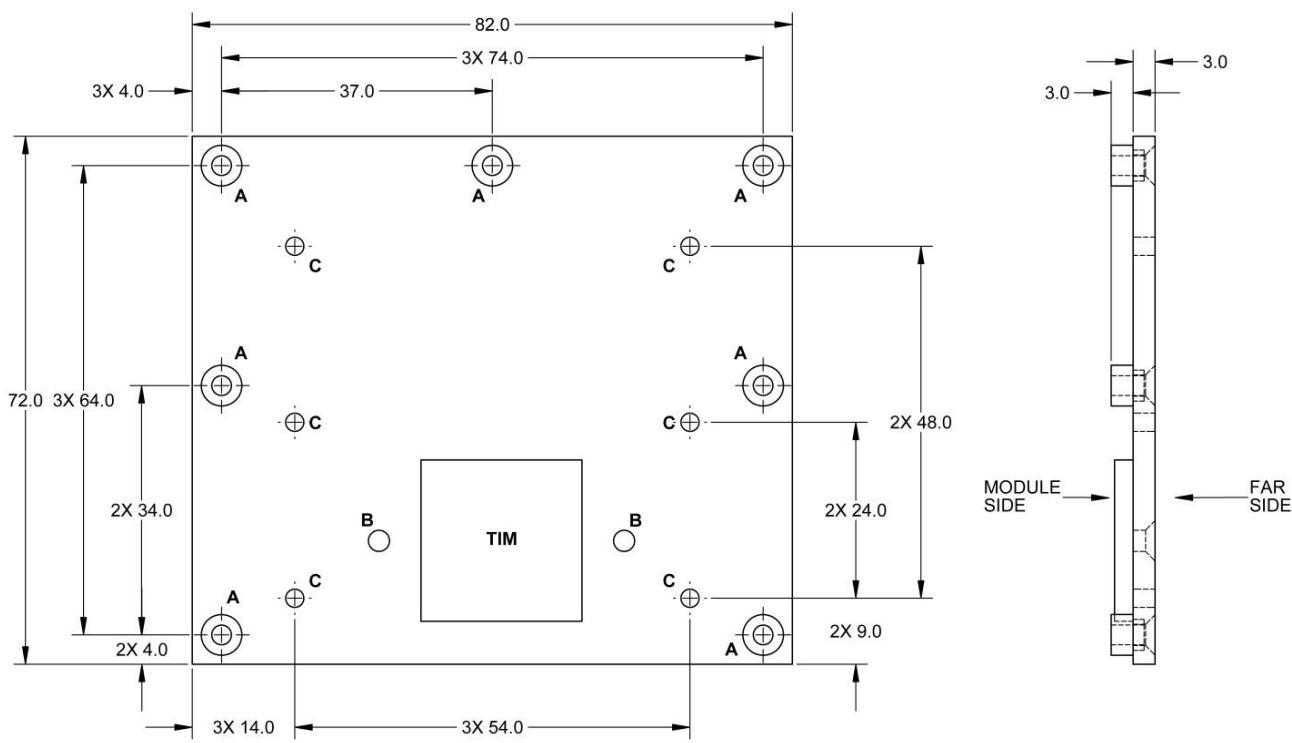
![82.0 3X 74.0 3X 4.0 37.0 72.0 3X 64.0 2X 34.0 2X 4.0 3X 14.0 3X 54.0 3.0 3.0 A C A C A C B TIM B C A C 2X 48.0 2X 24.0 2X 9.0 MODULE SIDE FAR SIDE](.smarc-hardware-specification-v1-1/ed7846598bd19b22d8bfecc6af23f7667d58debbc8147fd810957f5b26502539.jpg)

# 7 MODULE POWER

# 7.1 Input Voltage / Main Power Rail

The Module input power voltage is brought in on the ten VDD\_IN pins and returned through the numerous GND pins on the connector.

A Module shall withstand an indefinite exposure to an applied VDD\_IN that may vary over the 3.0V to 5.25V range, without damage.

A Module should operate over the entire VDD\_IN range of 3.0V to 5.25V.

Modules that use higher wattage SOCs may be designed to operate with a fixed 5V supply (4.75V to 5.25V).

Modules that are designed for rock-bottom cost and that use low power SOCs may be designed to operate with a fixed 3.3V supply (3.1V to 3.4V). They shall not be damaged in any way by exposure to the allowable VDD\_IN range of 3.0 to 5.25V.

Ten pins are allocated to VDD\_IN. The connector pin current rating is 0.5A per pin. This works out to 5A total for the 10 pins. At the lowest allowed Module input voltage of 3.0V, this would allow up to 15W of electrical power to be brought in (with no de-rating on the connector current capability). With a 40% connector current de-rating, up to 9W may be brought in at 3.0V.

If the fixed 5V input option is used, then 25W may be brought in over the 10 power pins (no de-rating). With a 40% connector de-rating, 15W are allowed to be brought in at 5V

As a practical matter, ARM most Module designs are expected to be 6W or less. X86 designs are expected to be in the 5W to 12W range, depending on the CPU SKU.

# 7.2 No Separate Standby Voltage

There is no separate voltage rail for standby power, other than the very low current (optional) RTC voltage rail. All Module operating and standby power comes from the single set of VDD\_IN pins. This suits battery power sources well, and is also easy to use with non-battery sources.

# 7.3 RTC Voltage Rail

RTC backup power may brought in on the VDD\_RTC rail. The RTC consumption is typically 15 microA or less. The allowable VDD\_RTC voltage range shall be 2.0V to 3.25V. The VDD\_RTC rail may be sourced from a Carrier based Lithium cell or Super Cap, or it may be left open if the RTC backup functions are not required. The Module shall be able to boot without an external VDD\_RTC voltage source.

Important: Lithium cells must be protected against charging by reverse currents, with a series Schottky diode and resistor. It is impractical to have the series diode on the Module, as this complicates the use of Super Caps (they need to be charged, over the Module VDD\_RTC pin).

Lithium cells, if used, shall be protected against charging by a Carrier Schottky diode. The diode is placed in series with the positive battery terminal. The diode anode is on the battery side, and the cathode on the Module VDD\_RTC side.

Note that if a Super cap is used, current may flow out of the Module VDD\_RTC rail to charge the Super Cap.

# 7.4 Power Sequencing

The Module signal CARRIER\_PWR\_ON exists to ensure that the Module is powered before the main body of Carrier circuits (those outside the power and power control path on the Carrier). The main body of Carrier board circuits should not be powered until the Module asserts the CARRIER\_PWR\_ON signal as a high. Module hardware should assert CARRIER\_PWR\_ON when all Module supplies necessary for Module booting are up. The Module should continue to assert signal CARRIER\_RESET\_OUT# after the release of CARRIER\_PWR\_ON, for a period sufficient to allow Carrier power circuits to come up.

# 7.5 System Power Domains

It is useful to describe an SMARC system as being divided into a hierarchy of three power domains:

1) Battery Charger power domain
2) SMARC Module power domain
3) Carrier Circuits power domain

The Battery Charger domain includes circuits that are active whenever either charger input power and / or battery power are available. These circuits may include power supply supervisor(s), battery chargers, fuel gauges and, depending on the battery configuration, switching power section(s) to step down a high incoming battery voltage.

The SMARC Module domain includes the SMARC module and may include a serial EEPROM on the Carrier, connected to the I2C\_PM I2C bus in the Module power domain, allowing Module software to read Carrier board parameters.

The Carrier Circuits domain includes “every thing else” (and does not include items from the Battery Charger and Module domain, even though they may be mounted on the Carrier).

This is illustrated in the figure below. Note: not shown in the figure is the additional, optional, fine grain power control that the Module may exert on the Carrier board, using design specific I/O. The power control I/O may be implemented via I2C I/O expanders (e.g. Texas Instruments TCA9554 or TC7408), or by other means.

Figure 13 System Power Domains
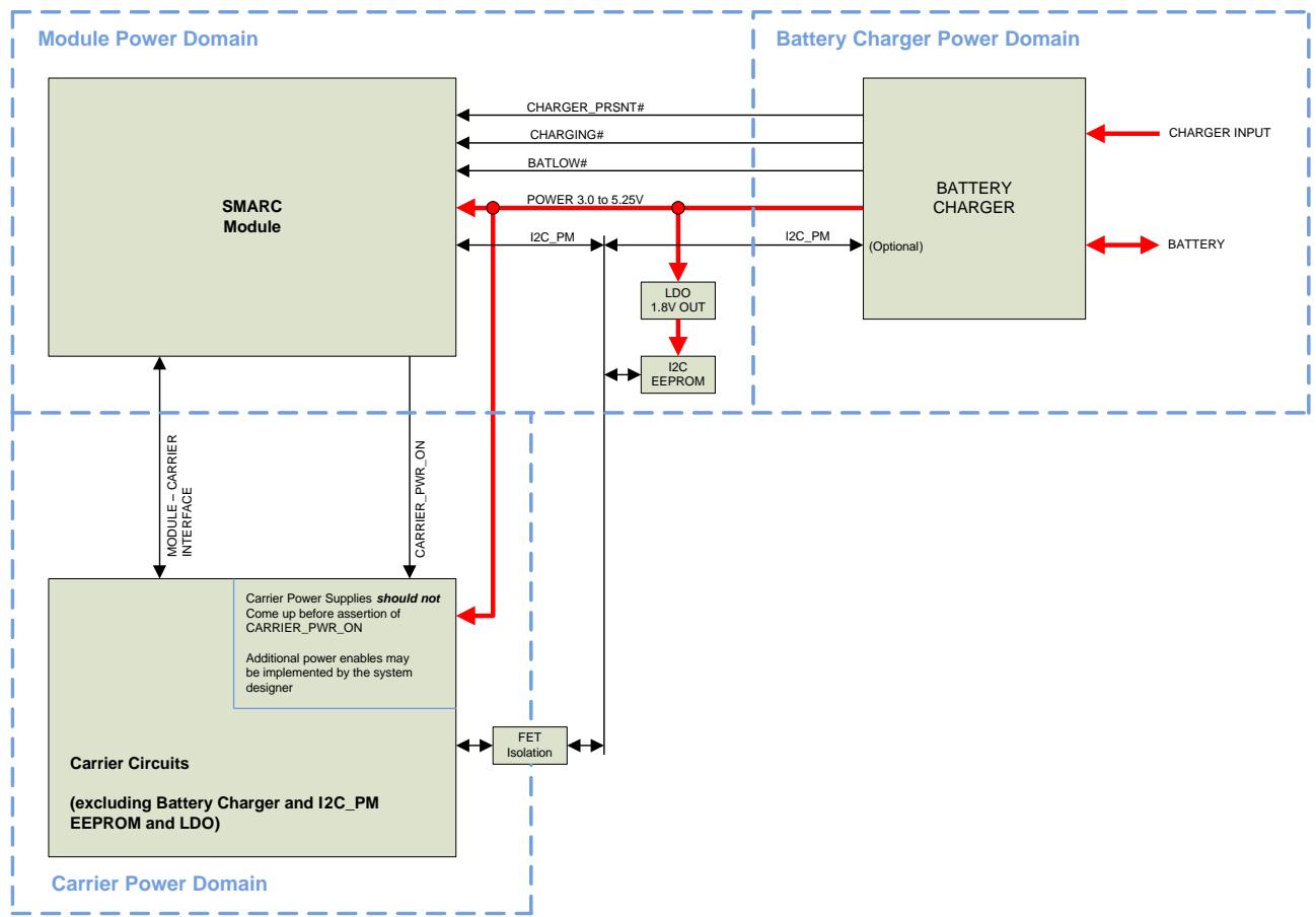
![Based on the provided flowchart, here is the accurate and concise description of the labeled blocks and connections:  **Power Domains** The diagram is divided into three dashed-line regions: *   **Module Power Domain** (Top Left) *   **Battery Charger Power Domain** (Top Right) *   **Carrier Power Domain** (Bottom Left)  **Labeled Blocks** *   **SMARC Module** *   **BATTERY CHARGER** (labeled as '(Optional)') *   **LDO** (labeled '1.8V OUT') *   **I2C EEPROM** *   **Carrier Circuits** (labeled '(excluding Battery Charger and I2C_PM EEPROM and LDO)') *   **FET Isolation**  **Connections**  *   **Between SMARC Module and BATTERY CHARGER:**     *   **CHARGER_PRSNT#** (Arrow pointing to SMARC Module)     *   **CHARGING#** (Arrow pointing to SMARC Module)     *   **BATLOW#** (Arrow pointing to SMARC Module)     *   **POWER 3.0 to 5.25V** (Bidirectional)     *   **I2C_PM** (Bidirectional)  *   **External to BATTERY CHARGER:**     *   **CHARGER INPUT** (Arrow pointing into BATTERY CHARGER)     *   **BATTERY** (Bidirectional)  *   **Within Battery Charger Power Domain:**     *   **POWER 3.0 to 5.25V** line connects downward to **LDO**.     *   **LDO** connects downward to **I2C EEPROM**.  *   **Between SMARC Module and Carrier Circuits:**     *   **MODULE - CARRIER INTERFACE** (Bidirectional)     *   **CARRIER_PWR_ON** (Arrow pointing from SMARC Module to Carrier Circuits)  *   **From Power Domain to Carrier Circuits:**     *   A thick red arrow from the **POWER 3.0 to 5.25V** line connects downward into the **Carrier Circuits** block.     *   **Note:** Inside the Carrier Circuits block: 'Carrier Power Supplies **should not** Come up before assertion of **CARRIER_PWR_ON**' and 'Additional power enables may be implemented by the system designer'.  *   **Between I2C Domain and Carrier Circuits:**     *   The vertical line dropping from **I2C_PM** connects bidirectionally to **I2C EEPROM**.     *   This line continues downward and connects bidirectionally to **FET Isolation**.     *   **FET Isolation** connects bidirectionally to **Carrier Circuits**.](.smarc-hardware-specification-v1-1/dbb85ef4631560f3aaf514f4232da834b966ad22d2802da721b3cabd5a574344.jpg)

# 8 MODULE AND CARRIER SERIAL EEPROMS

SMARC Modules shall include an I2C serial EEPROM on the Module I2C\_PM bus. The device used should be an Atmel 24C32 or equivalent. The device shall operate at 1.8V. The Module serial EEPROM should be placed at I2C slave addresses A2 A1 A0 set to 0 (I2C slave address 50 hex, 7 bit address format or A0 / A1 hex, 8 bit format) (recall that for I2C EEPROMs, address bits A6 A5 A4 A3 are set to binary 0101 convention).

The Module serial EEPROM is intended to retain Module parameter information, including a Module serial number. The Module serial EEPROM data structure should conform to the PICMG® EEEP Embedded EEPROM Specification.

SMARC Carriers may include an I2C serial EEPROM on the I2C\_PM bus, in the Module power domain. The device used should be an Atmel 24C32 or equivalent. The device shall operate at 1.8V. The Carrier serial EEPROM should be placed with I2C slave addresses A2 A1 A0 set to binary 111 (I2C slave address 57 hex, 7 bit address format or AE / AF hex, 8 bit format).

The Carrier serial EEPROM is intended to retain Carrier parameter information. The Carrier serial EEPROM data structure should conform to the PICMG® EEEP Embedded EEPROM Specification.

# 9 APPENDIX A: LVDS LCD COLOR MAPPINGS

# LVDS LCD Color Mappings

For flat panel use, parallel LCD data and control information (Red, green and blue color data; Display Enable, Vertical Synch, Horizontal Synch) are commonly serialized onto a set of LVDS differential pairs. The information is packed into frames that are 7 bits long. For 18 bit color depths, the data and control information utilize three LVDS channels (18 data bits + 3 control bits = 21 bits; hence 3 channels with 7 bit frames) plus a clock pair. For 24 bit color depths, four LVDS channels are used (24 data bits + 3 control bits + 1 unused bit = 28 bits, or 4 x 7) plus a clock pair.

The LVDS clock is transmitted as a separate LVDS pair. The LVDS clock period is 7 times longer than the pixel clock period. The LVDS clock edges are off from the 7 bit frame boundaries by 2 pixel periods.

Unfortunately, there are two different 24 bit color mappings in use. The more common one, sometimes referred to as “24 bit standard color mapping”, is not compatible with 18 bit panels, as it places the most significant RGB color data on the 4th LVDS data pair – the pair that is not used on 18 bit panels. There is a less common “24 bit / 18 bit compatible” mapping that puts the least significant color bits of the 24 bit set onto the 4th LVDS pair.

Some panels have pin straps that allow the user to select which color mapping is to be used.

The color mappings are summarized in the table below. The table includes a reference to a Texas Instruments LVDS transmitter, the SN75LVDS83B, showing the transmitter input pin names that TI lists in their sheet.

Single Channel LVDS LCD Color Mappings – General Information

<table><tr><td>LVDS Channel</td><td>Transmit Bit Order</td><td>18 bit Standard</td><td>24 Bit Standard</td><td>24 Bit / 18 Bit Compatible</td><td>SN75LVDS83B Pin Name</td></tr><tr><td rowspan="7">0</td><td>1</td><td>G0</td><td>G0</td><td>G2</td><td>D7</td></tr><tr><td>2</td><td>R5</td><td>R5</td><td>R7</td><td>D6</td></tr><tr><td>3</td><td>R4</td><td>R4</td><td>R6</td><td>D4</td></tr><tr><td>4</td><td>R3</td><td>R3</td><td>R5</td><td>D3</td></tr><tr><td>5</td><td>R2</td><td>R2</td><td>R4</td><td>D2</td></tr><tr><td>6</td><td>R1</td><td>R1</td><td>R3</td><td>D1</td></tr><tr><td>7</td><td>R0</td><td>R0</td><td>R2</td><td>D0</td></tr><tr><td rowspan="7">1</td><td>1</td><td>B1</td><td>B1</td><td>B3</td><td>D18</td></tr><tr><td>2</td><td>B0</td><td>B0</td><td>B2</td><td>D15</td></tr><tr><td>3</td><td>G5</td><td>G5</td><td>G7</td><td>D14</td></tr><tr><td>4</td><td>G4</td><td>G4</td><td>G6</td><td>D13</td></tr><tr><td>5</td><td>G3</td><td>G3</td><td>G5</td><td>D12</td></tr><tr><td>6</td><td>G2</td><td>G2</td><td>G4</td><td>D9</td></tr><tr><td>7</td><td>G1</td><td>G1</td><td>G3</td><td>D8</td></tr><tr><td rowspan="7">2</td><td>1</td><td>DE</td><td>DE</td><td>DE</td><td>D26</td></tr><tr><td>2</td><td>VS</td><td>VS</td><td>VS</td><td>D25</td></tr><tr><td>3</td><td>HS</td><td>HS</td><td>HS</td><td>D24</td></tr><tr><td>4</td><td>B5</td><td>B5</td><td>B7</td><td>D22</td></tr><tr><td>5</td><td>B4</td><td>B4</td><td>B6</td><td>D21</td></tr><tr><td>6</td><td>B3</td><td>B3</td><td>B5</td><td>D20</td></tr><tr><td>7</td><td>B2</td><td>B2</td><td>B4</td><td>D19</td></tr><tr><td rowspan="7">3</td><td>1</td><td></td><td></td><td></td><td>D23</td></tr><tr><td>2</td><td></td><td>B7</td><td>B1</td><td>D17</td></tr><tr><td>3</td><td></td><td>B6</td><td>B0</td><td>D16</td></tr><tr><td>4</td><td></td><td>G7</td><td>G1</td><td>D11</td></tr><tr><td>5</td><td></td><td>G6</td><td>G0</td><td>D10</td></tr><tr><td>6</td><td></td><td>R7</td><td>R1</td><td>D5</td></tr><tr><td>7</td><td></td><td>R6</td><td>R0</td><td>D27</td></tr></table>

Single Channel LVDS LCD 24 Bit Standard Color Mapping – Carrier Connections

<table><tr><td>LVDS Channel</td><td>Transmit Bit Order</td><td>24 Bit Colors</td><td>Module Pin Name</td><td>SN75LVDS83B Pin Name</td></tr><tr><td rowspan="7">0</td><td>1</td><td>G0</td><td>LCD_D[8]</td><td>D7</td></tr><tr><td>2</td><td>R5</td><td>LCD_D[21]</td><td>D6</td></tr><tr><td>3</td><td>R4</td><td>LCD_D[20]</td><td>D4</td></tr><tr><td>4</td><td>R3</td><td>LCD_D[19]</td><td>D3</td></tr><tr><td>5</td><td>R2</td><td>LCD_D[18]</td><td>D2</td></tr><tr><td>6</td><td>R1</td><td>LCD_D[17]</td><td>D1</td></tr><tr><td>7</td><td>R0</td><td>LCD_D[16]</td><td>D0</td></tr><tr><td rowspan="7">1</td><td>1</td><td>B1</td><td>LCD_D[1]</td><td>D18</td></tr><tr><td>2</td><td>B0</td><td>LCD_D[0]</td><td>D15</td></tr><tr><td>3</td><td>G5</td><td>LCD_D[13]</td><td>D14</td></tr><tr><td>4</td><td>G4</td><td>LCD_D[12]</td><td>D13</td></tr><tr><td>5</td><td>G3</td><td>LCD_D[11]</td><td>D12</td></tr><tr><td>6</td><td>G2</td><td>LCD_D[10]</td><td>D9</td></tr><tr><td>7</td><td>G1</td><td>LCD_D[9]</td><td>D8</td></tr><tr><td rowspan="7">2</td><td>1</td><td>DE</td><td>LCD_DE</td><td>D26</td></tr><tr><td>2</td><td>VS</td><td>LCD_VS</td><td>D25</td></tr><tr><td>3</td><td>HS</td><td>LCD_HS</td><td>D24</td></tr><tr><td>4</td><td>B5</td><td>LCD_D[5]</td><td>D22</td></tr><tr><td>5</td><td>B4</td><td>LCD_D[4]</td><td>D21</td></tr><tr><td>6</td><td>B3</td><td>LCD_D[3]</td><td>D20</td></tr><tr><td>7</td><td>B2</td><td>LCD_D[2]</td><td>D19</td></tr><tr><td rowspan="7">3</td><td>1</td><td></td><td></td><td>D23</td></tr><tr><td>2</td><td>B7</td><td>LCD_D[7]</td><td>D17</td></tr><tr><td>3</td><td>B6</td><td>LCD_D[6]</td><td>D16</td></tr><tr><td>4</td><td>G7</td><td>LCD_D[15]</td><td>D11</td></tr><tr><td>5</td><td>G6</td><td>LCD_D[14]</td><td>D10</td></tr><tr><td>6</td><td>R7</td><td>LCD_D[23]</td><td>D5</td></tr><tr><td>7</td><td>R6</td><td>LCD_D[22]</td><td>D27</td></tr></table>

For a 24 bit standard color map single channel LVDS implementation, connect the Module pins to the Carrier board LVDS transmitter input pins as shown in the table above.

The LVDS transmitter clock input (pin name CLKIN on the TI SN75LVDS83B) should be driven by the Module parallel LCD interface pixel clock: the Module LCD\_PCK pin.

Some LVDS transmitters, including the SN75LVDS83B, have a pin allowing the user to select which edge of the pixel clock is to be used to latch the data coming in to the LVDS transmitter. In most cases, this pin should be set for a rising edge clock latching. A resistor or jumper option allowing either edge to be used is recommended.

# Dual Channel LVDS LCD 24 Bit Standard Color Mapping – Carrier Connections

Dual channel LVDS implementations are used to drive high resolution panels (generally, panel resolutions of 1280 x 1024 and above). In a dual channel implementation, the parallel pixel data is fed to a pair of LVDS transmitters. The pair of transmitters form two sets of LVDS streams (“dual channel”). The first set has the odd pixel information and the second set has the even pixel information. By convention, the upper left most pixel on a display is “odd”, the next one on the line is “even”, and so on.

A 24 bit dual channel LVDS implementation comprises 10 differential pairs: 4 pairs for odd pixel and control data; 1 pair for the LVDS clock for the odd data; 4 pairs for the even pixel data and control data, and 1 pair for the even LVDS clock.

The data is clocked into the pair of Carrier Board LVDS transmitters by Module signal LCD\_DUAL\_PCK. The rising edge of this clock is used to latch the odd pixels, and the falling edge for the even pixels,

The same 18 / 24 bit color mapping considerations described earlier in this document apply to dual channel displays. However, as dual channel displays are higher end products, they tend to be 24 bit devices, usually with the standard 24 bit color mapping.

# 10 APPENDIX B: ALTERNATE FUNCTION BLOCK USE MODELS

# 10.1 Alternate Function Block: MOST Media Local Bus MLB-150 Use

The MOST Media Local Bus is used in the automotive industry for infotainment. MLB-150 is the high speed, differential version of the standard. An SMARC AFB implementation may be realized per the tables below.

<table><tr><td>Signal Name</td><td>Direction</td><td>Type</td><td>Description</td><td>AFB Mapping</td></tr><tr><td>MLB_CK+MLB_CK-</td><td>Output</td><td>LVDS MLB</td><td>MOST Bus MediaLB Clock differential pair</td><td>AFB_DIFF2+AFB_DIFF2-</td></tr><tr><td>MLB_DAT+MLB_DAT-</td><td>Bi-Dir</td><td>LVDS MLB</td><td>MOST Bus MediaLB Data differential pair</td><td>AFB_DIFF3+AFB_DIFF3-</td></tr><tr><td>MLB_SIG+MLB_SIG-</td><td>Bi-Dir</td><td>LVDS MLB</td><td>MOST Bus MediaLB Signal differential pair</td><td>AFB_DIFF4+AFB_DIFF4-</td></tr><tr><td>MLB_RST#</td><td>Output</td><td>Protected CMOS 1.8V</td><td>Low level to reset MLB</td><td>AFB8_PTIO</td></tr><tr><td>MLB_PWRDN#</td><td>Output</td><td>Protected CMOS 1.8V</td><td>Low level for MLB Power down</td><td>AFB9_PTIO</td></tr></table>

An I2C interface is needed for MOST bus support. The Module I2C\_GP port may be used.

<table><tr><td>Signal Name</td><td>Direction</td><td>Type</td><td>Description</td></tr><tr><td>I2C_GP_DAT</td><td>Bi-Dir</td><td>CMOS</td><td rowspan="2">General purpose I2C may be used for MOST support.</td></tr><tr><td>I2C_GP_CK</td><td>OD</td><td>1.8V</td></tr></table>

# 10.2 Alternate Function Block: Dual GBE Use

The magnetics referred to in the table below are based on the Carrier board.

<table><tr><td>Signal Name</td><td>Direction</td><td>Type</td><td>Description</td><td>AFB Mapping</td></tr><tr><td>GBE_1_MDI0+GBE_1_MDI0-</td><td>Bi-Dir</td><td>GBE MDI</td><td>Bi-directional transmit/receive pair 0 to magnetics (Media Dependent Interface) for  $AFB 2^{nd}$  GBE</td><td>AFB_DIFF0+AFB_DIFF0-</td></tr><tr><td>GBE_1_MDI1+GBE_1_MDI1-</td><td>Bi-Dir</td><td>GBE MDI</td><td>Bi-directional transmit/receive pair 1 to magnetics (Media Dependent Interface) for  $AFB 2^{nd}$  GBE</td><td>AFB_DIFF1+AFB_DIFF1-</td></tr><tr><td>GBE_1_MDI2+GBE_1_MDI2-</td><td>Bi-Dir</td><td>GBE MDI</td><td>Bi-directional transmit/receive pair 2 to magnetics (Media Dependent Interface) for  $AFB 2^{nd}$  GBE</td><td>AFB_DIFF2+AFB_DIFF2-</td></tr><tr><td>GBE_1_MDI3+GBE_1_MDI3-</td><td>Bi-Dir</td><td>GBE MDI</td><td>Bi-directional transmit/receive pair 3 to magnetics (Media Dependent Interface) for  $AFB 2^{nd}$  GBE</td><td>AFB_DIFF3+AFB_DIFF3-</td></tr><tr><td>GBE_1_CTREF</td><td>Output</td><td>Ref Voltage</td><td>Central-Tap reference voltage for Carrier board Ethernet magnetic for  $AFB 2^{nd}$  GBE</td><td>AFB0_OUT</td></tr><tr><td>GBE_1_LINK100#</td><td>Output OD</td><td>CMOS3.3V Tolerant</td><td>Link Speed Indication LED for 100Mbps for  $AFB 2^{nd}$  GBE</td><td>AFB6_PTIO</td></tr><tr><td>GBE_1_LINK1000#</td><td>Output OD</td><td>CMOS3.3V Tolerant</td><td>Link Speed Indication LED for 1000Mbps for  $AFB 2^{nd}$  GBE</td><td>AFB7_PTIO</td></tr><tr><td>GBE_1_LINK#_ACT</td><td>Output OD</td><td>CMOS3.3V Tolerant</td><td>Link / Activity Indication LED for  $AFB 2^{nd}$  GBEDriven low on Link (10, 100 or 1000 mbps)Blinks on Activity</td><td>AFB8_PTIO</td></tr></table>

# 10.3 Alternate Function Block: Industrial Network Use

The Alternate Function Block may be used to implement Industrial Network features. Industrial Networks are optimized for real-time control of industrial systems, and include features such as Real Time Ethernet channels and Fieldbus implementations.

Ethernet magnetic are implemented on the Carrier board.

<table><tr><td>Signal Name</td><td>Direction</td><td>Type</td><td>Description</td><td>AFB Mapping</td></tr><tr><td>RTE0_TXD+ RTE0_TXD-</td><td>Output</td><td>10 /100Base-TX</td><td>Real Time Ethernet 0 MDI transmit data pair</td><td>AFB_DIFF0+ AFB_DIFF0-</td></tr><tr><td>RTE0_RXD+ RTE0_RXD-</td><td>Input</td><td>10 /100Base-TX</td><td>Real Time Ethernet 0 MDI receive data pair</td><td>AFB_DIFF1+ AFB_DIFF1-</td></tr><tr><td>RTE1_TXD+ RTE1_TXD-</td><td>Output</td><td>10 /100Base-TX</td><td>Real Time Ethernet 1 MDI transmit data pair</td><td>AFB_DIFF2+ AFB_DIFF2-</td></tr><tr><td>RTE1_RXD+ RTE1_RXD-</td><td>Input</td><td>10 /100Base-TX</td><td>Real Time Ethernet 1 MDI receive data pair</td><td>AFB_DIFF3+ AFB_DIFF3-</td></tr><tr><td>RTE_SYNC_0</td><td>Output</td><td>CMOS 1.8V</td><td>Real Time Ethernet synchronization signal 0</td><td>AFB0_OUT</td></tr><tr><td>RTE_SYNC_1</td><td>Output</td><td>CMOS 1.8V</td><td>Real Time Ethernet synchronization signal 1</td><td>AFB1_OUT</td></tr><tr><td>RTE0_LINK#</td><td>Output</td><td>CMOS</td><td>Real Time Ethernet link indication channel 0</td><td>AFB6_PTIO</td></tr><tr><td>RTE0_ACT#</td><td>Output</td><td>CMOS</td><td>Real Time Ethernet activity indication channel 0</td><td>AFB7_PTIO</td></tr><tr><td>RTE1_LINK#</td><td>Output</td><td>CMOS</td><td>Real Time Ethernet link indication channel 1</td><td>AFB8_PTIO</td></tr><tr><td>RTE1_ACT#</td><td>Output</td><td>CMOS</td><td>Real Time Ethernet activity indication channel 1</td><td>AFB9_PTIO</td></tr><tr><td>FB_TXD</td><td>Output</td><td>CMOS 1.8V</td><td>Fieldbus transmit data</td><td>AFB2_OUT</td></tr><tr><td>FB_RXD</td><td>Input</td><td>CMOS 1.8V</td><td>Fieldbus receive data</td><td>AFB3_IN</td></tr><tr><td>FB_IO0</td><td>Bi-Dir</td><td>CMOS 1.8V</td><td>Fieldbus control 0; network dependent. Used as a transmitter enable output or as a failure input signal.</td><td>AFB4_IN</td></tr><tr><td>FB_IO1</td><td>Bi-Dir</td><td>CMOS 1.8V</td><td>Fieldbus control 1. Reserved</td><td>AFB5_IN</td></tr></table>

Real Time Ethernet and Fieldbus implementations typically use a number of LEDs to indicate the system status. Four SMARC GPIOs are selected to support such LEDs. The LED usage conventions vary by the Fieldbus type, and are not covered in this document.

<table><tr><td>Signal Name</td><td>Direction</td><td>Type</td><td>Description</td><td>GPIO Mapping</td></tr><tr><td>FB_LED0_G#</td><td>Output</td><td>CMOS1.8V</td><td>Communication status 0Used to drive green LED</td><td>GPIO0</td></tr><tr><td>FB_LED0_R#</td><td>Output</td><td>CMOS1.8V</td><td>Communication status 0Used to drive red LED</td><td>GPIO1</td></tr><tr><td>FB_LED1_G#</td><td>Output</td><td>CMOS1.8V</td><td>Communication status 1Used to drive green LED</td><td>GPIO2</td></tr><tr><td>FB_LED1_R#</td><td>Output</td><td>CMOS1.8V</td><td>Communication status 1Used to drive red LED</td><td>GPIO3</td></tr></table>

A Fieldbus bus implementation may need additional I/Os, address switches, or status LEDs. These may be realized on the Carrier board using I2C bus peripheral devices. The Module I2C\_GP port may be used to support this.

<table><tr><td>Signal Name</td><td>Direction</td><td>Type</td><td>Description</td></tr><tr><td>I2C_GP_DAT</td><td>Bi-Dir</td><td>CMOS</td><td>General purpose I2C may be used for MOST support.</td></tr><tr><td>I2C_GP_CK</td><td>OD</td><td>1.8V</td><td></td></tr></table>

# 10.4 Alternate Function Block: Intel Bay Trail Use

The following table outlines the recommended mapping of SMARC AFB pins for Intel Bay Trail use.

<table><tr><td>AFB Signal</td><td>Type / Dir</td><td>SMARC Standard Use</td><td>SMARC with Intel Bay Trail</td><td>Notes</td></tr><tr><td>AFB0_OUT</td><td>Out</td><td>Reserved</td><td>Intel SOC PMC_SLP_S3#</td><td>Intel sleep state status S3: suspend to RAM</td></tr><tr><td>AFB1_OUT</td><td>Out</td><td>Reserved</td><td>Intel SOC PMC_SLP_S4#</td><td>Intel sleep state status S3: suspend to disk</td></tr><tr><td>AFB2_OUT</td><td>Out</td><td>Reserved</td><td>Intel SOC PMC_SUS_STAT#</td><td>Intel Suspend Status signal</td></tr><tr><td>AFB3_IN</td><td>In</td><td>Reserved</td><td></td><td></td></tr><tr><td>AFB4_IN</td><td>In</td><td>Reserved</td><td></td><td></td></tr><tr><td>AFB5_IN</td><td>In</td><td>Reserved</td><td></td><td></td></tr><tr><td>AFB6_PTIO</td><td>Protected Bi-Dir</td><td>Reserved</td><td>EN_OC# for USB SS on AFB</td><td>USB 3 port power enable and overcurrent</td></tr><tr><td>AFB7_PTIO</td><td>Protected Bi-Dir</td><td>Reserved</td><td>PCU_SMB_ALERT#</td><td>SM Bus Alert# (interrupt) signal</td></tr><tr><td>AFB8_PTIO</td><td>Protected Bi-Dir</td><td>Reserved</td><td></td><td></td></tr><tr><td>AFB9_PTIO</td><td>Protected Bi-Dir</td><td>Reserved</td><td></td><td></td></tr><tr><td>AFB_DIFF0+ AFB_DIFF0-</td><td>HS Pair Out or Bi-Dir</td><td>Reserved</td><td>Intel SOC USB3_TXP Intel SOC USB3_TXN</td><td rowspan="3">These Super Speed pairs and USB 2 pair form a single USB 3 port. Coupling caps for USB 3 TX and RX pairs are off-Module.</td></tr><tr><td>AFB_DIFF1+ AFB_DIFF1-</td><td>HS Pair In or Bi-Dir</td><td>Reserved</td><td>Intel SOC USB3_RXP Intel SOC USB3_RXN</td></tr><tr><td>AFB_DIFF2+ AFB_DIFF2-</td><td>HS Pair Out or Bi-Dir</td><td>Reserved</td><td>Intel SOC USB_DP0 Intel SOC USB_DNO</td></tr><tr><td>AFB_DIFF3+ AFB_DIFF3-</td><td>HS Pair In or Bi-Dir</td><td>Reserved</td><td>Intel SATA1 TXP Intel SATA1 TXN</td><td>Coupling caps are on-Module</td></tr><tr><td>AFB_DIFF4+ AFB_DIFF4-</td><td>HS Pair In, Out or Bi-Dir</td><td>Reserved</td><td>Intel SATA1 RXP Intel SATA1 RXN</td><td>Coupling caps are on-Module</td></tr></table>

# 10.4.1 Additional SMARC to Intel Bay Trail Mapping Recommendations: I2C

The Intel Bay Trail SOC has seven I2C ports, designated I2C0 through I2C6 by Intel. Additionally, there is an SM Bus, which is an I2C superset and has I2C compatibility modes. A recommended mapping of Intel I2C ports to SMARC I2C ports is shown in the figure below. Intel ports I2C5 and I2C6 are not used.

The peripheral blocks at the top of the figure are from a specific design and may be regarded as for illustration only in this context. They are not part of the SMARC specification.

The SMARC I2C\_PM bus and the x86 SM Bus serve similar functions, and the recommendation is to merge them on SMARC designs, as shown in the figure.

Figure 14 SMARC I2C Intel Bay Trail I2C Mapping Recommendation
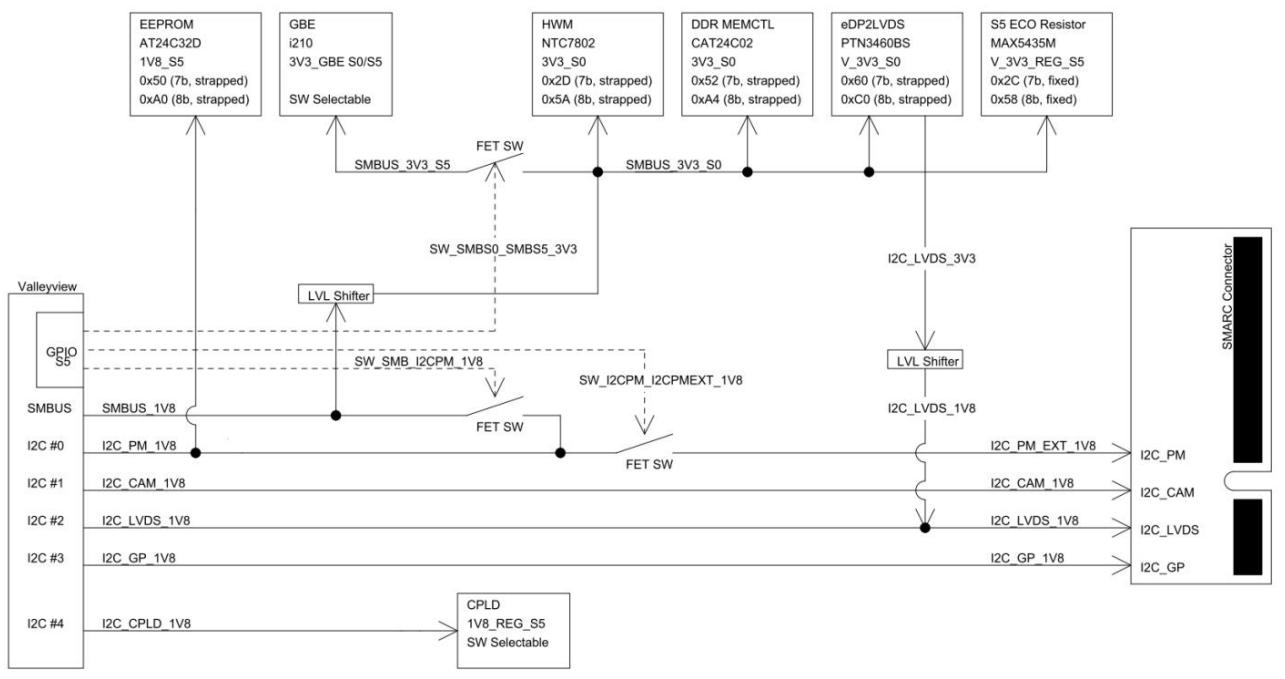
![The flowchart/block diagram illustrates the I2C/SMBus connections between a processor platform (Valleyview), various components, and a SMARC connector.  **Labeled Blocks:** *   **Valleyview** (containing a sub-block **GPIO S5**) *   **EEPROM AT24C32D 1V8_S5 0x50 (7b, stranded) 0xA0 (8b, stranded)** *   **GBE i210 3V3_GBE S0/S5 SW Selectable** *   **HWM NTC7802 3V3_S0 0x2D (7b, stranded) 0x5A (8b, stranded)** *   **DDR MEMCTL CAT24C02 3V3_S0 0x52 (7b, stranded) 0xA4 (8b, stranded)** *   **eDP2LVDS PTN3460BS V_3V3_S0 0x60 (7b, stranded) 0xC0 (8b, stranded)** *   **S5 ECO Resistor MAX5435M V_3V3_REG_S5 0x2C (7b, fixed) 0x58 (8b, fixed)** *   **CPLD 1V8_REG_S5 SW Selectable** *   **SMARC Connector** *   Two blocks labeled **LVL Shifter** *   Three switches labeled **FET SW**  **Connections:** *   **Top Row Bus:** A line labeled **SMBUS_3V3_S5** originates from **GBE** and passes through a **FET SW** switch (controlled by dashed line **SW_SMBS0_SMBS5_3V3**) to become **SMBUS_3V3_S0**. This **SMBUS_3V3_S0** line connects to the bottom of **HWM**, **DDR MEMCTL**, **eDP2LVDS**, and **S5 ECO Resistor**. *   **Valleyview Connections:**     *   **GPIO S5** has dashed control lines pointing to the **LVL Shifter** (top), the top **FET SW**, and the middle **FET SW** switches.     *   **SMBUS** and **I2C #0** connect to a common line labeled **SMBUS_1V8** / **I2C_PM_1V8**.     *   **I2C #1** connects to **I2C_CAM_1V8**.     *   **I2C #2** connects to **I2C_LVDS_1V8**.     *   **I2C #3** connects to **I2C_GP_1V8**.     *   **I2C #4** connects to **I2C_CPLD_1V8**, which leads to the **CPLD** block. *   **Middle Switching & Level Shifting:**     *   The **SMBUS_1V8** / **I2C_PM_1V8** line connects upward to a **LVL Shifter**.     *   This line continues right through two **FET SW** switches (controlled by dashed lines **SW_SMB_I2CPM_1V8** and **SW_SMB_I2CPMEXT_1V8**) to become **I2C_PM_EXT_1V8**.     *   **eDP2LVDS** connects downward to **I2C_LVDS_3V3**, which passes through the second **LVL Shifter** to become **I2C_LVDS_1V8**. This line connects to the horizontal **I2C_LVDS_1V8** line from Valleyview. *   **SMARC Connector Connections:**     *   A curly bracket groups the output lines connecting to the **SMARC Connector**.     *   **I2C_PM_EXT_1V8** connects to **I2C_PM**.     *   **I2C_CAM_1V8** connects to **I2C_CAM**.     *   **I2C_LVDS_1V8** connects to **I2C_LVDS**.     *   **I2C_GP_1V8** connects to **I2C_GP**.](.smarc-hardware-specification-v1-1/ad402aba982dce415a9f08ae2268fb4e904b0149f0fd96b74f9e3a683095e1e4.jpg)

The SMARC I2C\_PM bus is meant as a power management bus. It may be active whenever the system has power (including the S5 “soft off” and S6 “deep soft off” states). The SOC connection should not drag down the SMARC I2C\_PM bus (labeled I2C\_PM\_EXT\_1V8 in the figure above – the FET switch should be open when the SOC is in the S6 state).

# 10.5 Alternate Function Block Summary Comparisons

Alternate Function Block – Possible Uses Comparison Chart

<table><tr><td>AFB Signal</td><td>Type / Dir</td><td>USB 3.0</td><td>MOST / MLB</td><td>Dual GBE</td><td>Industrial Network</td><td>DSI</td><td>Intel Bay Trail</td></tr><tr><td>AFB0_OUT</td><td>Out</td><td></td><td></td><td>GBE_1_CTREF</td><td>RTE_SYNC_0</td><td></td><td>Intel SOC PMC_SLP_S3#</td></tr><tr><td>AFB1_OUT</td><td>Out</td><td></td><td></td><td></td><td>RTE_SYNC_1</td><td></td><td>Intel SOC PMC_SLP_S4#</td></tr><tr><td>AFB2_OUT</td><td>Out</td><td></td><td></td><td></td><td>FB_TXD</td><td></td><td>Intel SOC PMC_SUS_STAT#</td></tr><tr><td>AFB3_IN</td><td>In</td><td></td><td></td><td></td><td>FB_RXD</td><td></td><td></td></tr><tr><td>AFB4_IN</td><td>In</td><td></td><td></td><td></td><td>FB_IO0 (Bi-Dir)</td><td></td><td></td></tr><tr><td>AFB5_IN</td><td>In</td><td></td><td></td><td></td><td>FB_IO1 (Bi-Dir)</td><td></td><td></td></tr><tr><td>AFB6_PTIO</td><td>Protected Bi-Dir</td><td></td><td></td><td>GBE_1_LINK100#</td><td>RTE0_LINK#</td><td></td><td>EN_OC# for USB SS on AFB</td></tr><tr><td>AFB7_PTIO</td><td>Protected Bi-Dir</td><td></td><td></td><td>GBE_1_LINK1000#</td><td>RTE0_ACT#</td><td></td><td>PCU_SMB_ALERT#</td></tr><tr><td>AFB8_PTIO</td><td>Protected Bi-Dir</td><td></td><td>MLB_RST#</td><td>GBE_1_LINK_ACT#</td><td>RTE1_LINK#</td><td></td><td></td></tr><tr><td>AFB9_PTIO</td><td>Protected Bi-Dir</td><td></td><td>MLB_PWRDN#</td><td></td><td>RTE1_ACT#</td><td></td><td></td></tr><tr><td>AFB_DIFF0+ AFB_DIFF0-</td><td>HS Pair Out or Bi-Dir</td><td>USB1_SSTX0+ USB1_SSTX0-</td><td></td><td>GBE_1_MDIO+ GBE_1_MDIO-</td><td>RTE0_TXD+ RTE0_TXD-</td><td></td><td>Intel SOC USB3_TXP Intel SOC USB3_TXN</td></tr><tr><td>AFB_DIFF1+ AFB_DIFF1-</td><td>HS Pair In or Bi-Dir</td><td>USB1_SSRX0+ USB1_SSRX0-</td><td></td><td>GBE_1_MDI1+ GBE_1_MDI1-</td><td>RTE0_RXD+ RTE0_RXD-</td><td></td><td>Intel SOC USB3_RXP Intel SOC USB3_RXN</td></tr><tr><td>AFB_DIFF2+ AFB_DIFF2-</td><td>HS Pair Out or Bi-Dir</td><td>USB2_SSTX0+ USB2_SSTX0-</td><td>MOST_MLB_CK+ MOST_MLB_CK-</td><td>GBE_1_MDI2+ GBE_1_NDI2-</td><td>RTE1_TXD+ RTE1_TXD-</td><td>DSI_CK+ DSI_CK-</td><td>Intel SOC USB_DP0 Intel SOC USB_DNO</td></tr><tr><td>AFB_DIFF3+ AFB_DIFF3-</td><td>HS Pair In or Bi-Dir</td><td>USB2_SSRX0+ USB2_SSRX0-</td><td>MOST_MLB_DAT+ MOST_MLB_DAT-</td><td>GBE_1_MDI3+ GBE_1_MDI3-</td><td>RTE1_RXD+ RTE1_RXD-</td><td>DSI_D0+ DSI_D0-</td><td>Intel SATA1 TXP Intel SATA1 TXN</td></tr><tr><td>AFB_DIFF4+ AFB_DIFF4-</td><td>HS Pair In, Out or Bi-Dir</td><td></td><td>MOST_MLB_SIG+ MOST_MLB_SIG-</td><td></td><td></td><td>DSI_D1+ DSI_D1-</td><td>Intel SATA1 RXP Intel SATA1 RXN</td></tr></table>

Please refer to the individual AFB interface sections above for details such as coupling cap locations.

# 11 APPENDIX C: DOCUMENT CHANGES

# 11.1 SMARC HW Specification Changes V1.0 to V1.1

<table><tr><td>Section Ref</td><td>Change Description</td></tr><tr><td>Various</td><td>Sections and Section Numbers that existed in V1.0 still exist in V1.1x</td></tr><tr><td>Various</td><td>Figure Numbers have changed as one Figure was removed and four Figures were added</td></tr><tr><td>Various</td><td>Version changed to V1.1x with Feb 4, 2014 date mark</td></tr><tr><td></td><td>Copyright © notice changed to 2014</td></tr><tr><td>TOC</td><td>Table of Contents updated</td></tr><tr><td>TOF</td><td>Table of Figures updated</td></tr><tr><td>Various</td><td>VDD_IO references all changed to 1.8V</td></tr><tr><td>2.3</td><td>Pin Group Summary updated</td></tr><tr><td>3.1</td><td>Required and Optional Features Table updatedRTC added to tableDP over HDMI pins added to table</td></tr><tr><td>4.1</td><td>Signal Direction and Type Definitions updated:VDD_IO reference removedPrevious VDD_IO references change to 1.8VCMOS 1.5V* Type added for HD Audio</td></tr><tr><td>4.2.4</td><td>Carrier Board Dual Channel LVD Support section re-writtenReferences to LCD_DUAL_PCK removedFormer Figure 1 removedText updated</td></tr><tr><td>4.2.7</td><td>Expanded this section, described DP operation over HDMI pins</td></tr><tr><td>4.3.3</td><td>Former Figure 2 (now Figure 1) changed VDD_IO reference to CARRIER 1.8V</td></tr><tr><td>4.5.1</td><td>Added text to indicate that SPI0_CS0# signals should be used to select Carrier SPI boot device</td></tr><tr><td>4.7</td><td>HDA InterfaceType / Tolerance changed to CMOS 1.5V*New text added</td></tr><tr><td>4.21</td><td>Section renamed to 4.21 I/O LevelsTable removedText re-written to describe the various voltage levels used</td></tr><tr><td>4.24.2</td><td>Module TerminationsTable revisedSDIO_WP addedSDIO_CD# added</td></tr><tr><td>5.1</td><td>Module Pin-OutSignal LCD_DUAL_PCK (pin S142) removed. Pin S142 now marked as RSVD.Signal VDD_IO_SEL# (pin S158) was removed. Pin S158 now listed as GND</td></tr><tr><td>6.1</td><td>Added note about JAE MM70 connector</td></tr><tr><td>6.3</td><td>Added figure from Adlink on recommended edge finger keep out area for 82mm x 50mm Modules</td></tr><tr><td>6.4</td><td>Added figure from Adlink on recommended edge finger keep out area for 82mm x 80mm Modules</td></tr><tr><td>6.10</td><td>New Section: Heat Spreader - 82mm x 50mm ModuleThree Figures added</td></tr><tr><td>6.11</td><td>New Section: Heat Spreader - 82mm x 80mm ModuleNew Figure added</td></tr><tr><td>7.1</td><td>Input Voltage / Main Power Rail• Section re-written• 5V fixed option described• 3.3V fixed option described</td></tr><tr><td>7.3 and Various</td><td>Clarified that RTC is optional</td></tr><tr><td>10.4</td><td>Added new Section 10.4 (old 10.4 becomes 10.5). New section outlines use of SMARC AFB with Intel Bay Trail</td></tr><tr><td>10.4.1</td><td>Added section with additional Intel Bay Trail recommendations on I2C Mappings</td></tr><tr><td>10.5</td><td>Old section 10.4 becomes 10.5. Updated AFB use case comparison table to include Intel Bay Trail.</td></tr></table>
[🔗 Link to the original document](.smarc-hardware-specification-v1-1/smarc-hardware-specification-v1-1.pdf)