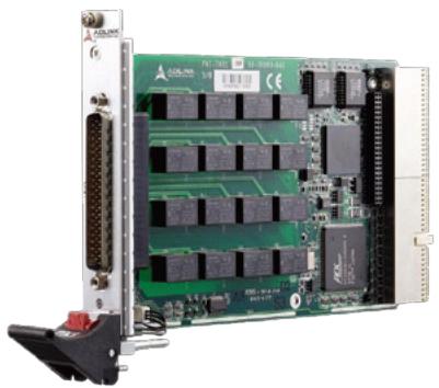
# Features
■ PXI specifications Rev. 2.2 compliant
■ 3U Eurocard form factor, CompactPCI compliant (PICMG 2.0 R3.0)
PICMG 2.1 R2.0 CompactPCI Hot Swap specifications compliant
■ 16-CH SPDT (I Form C) non-latching relays
■ Switching capacity
• 3 A switching, 3 A carrying
\- 220 V $_{DC}$ , 250 V $_{AC}$
■ 125 operations per second for full settling
Onboard I k-sample scan list for deterministic scanning
■ Handshaking signals for external instruments synchronization
■ Design for safety-critical applications
Hardware emergency shutdown with programmable relay safety status
- Watchdog timer from 1 ms to 420 s with programmable relay safety status
8 auxiliary 3.3 V/TTL digital inputs/outputs with 5 V tolerance
■ Multiple modules synchronization through PXI trigger bus and star trigger
■ Fully software programmable
Operating Systems
\- Windows 7/10 x64/x86
Driver and SDK
- VB/VC++
- LabVIEW
# Introduction
ADLINK's PXI-7901 is a general-purpose (GP) switch module implementing 16-CH independent single-pole double-throw (SPDT) relays (I Form C). The PXI-7901 can connect one input to one output and be used as signal switching and routing for measurement systems or ATE. Thanks to its high switching capacity, PXI-7901 can also be used to turn on or turn off devices such as motors, fans, heaters, and lights.
The contact position of the relays can be changed either by direct software commands or by following the instructions previously stored in the onboard scan list. The scan list advances upon the trigger from external measurement devices, such as a DMM. The scan list could also advance when the scan-delay timer expires. In the PXI-7901, PXI trigger functions are supported and software programmable. Multiple modules can therefore be synchronized without additional field wiring.
# Specifications
# Relay Characteristics
Number of channels: 16
■ Relay type: SPDT (I Form C), non-latching
Switching capacity
· Max. switching current: 3 A
· Max. switching voltage: 220 VDC, 250 VAC
· Max. switching power: 50 VA, 60 W
· Max. carrying current: 3 A
Contact resistance: 150 mΩ max.
Relay set/reset time
· Operate time: 5 ms max.
- Release time: 5 ms max.
· Bounce time: 3 ms max.
Expected life
· Mechanical life: $10^{8}$ operations min.
· Electrical life: $10^{5}$ operations min. (0.4 A @ 125 V $_{AC}$ , resistive load)
Data transfer: Programmed I/O
# Auxiliary Digital I/O
■ Numbers of channel: 8 inputs/outputs
■ Compatibility: 3.3 V/TTL (5 V tolerant)
# Handshaking Signals
Programmable polarity
■ Logic level: 3.3 V/TTL (5 V tolerant)
■ TRG\_IN source: AUXI, PXI trigger bus, PXI star trigger input
■ S\_ADV destination: AUX0, PXI trigger bus
# Safety Functions
Emergency shutdown
· Logic level: 3.3 V/TTL (5 V tolerant)
· Active: logic low
Watchdog timer
· Base clock available: 10 MHz, fixed
- Counter width: 32-bit
# General Specifications
I/O Connector: 62-pin D-sub male
- Operating temperature: 0°C to 55°C
■ Storage temperature: -20°C to 70°C
■ Relative humidity: 5% to 85% non-condensing
■ Power requirements: (when all relays are ON)
| Device | +5 V | +3.3 V |
| PXI-7901 | 700 mA | 400 mA |
■ Dimensions (not including connectors)
· 160 mm × 100 mm
# Certifications
EMC/EMI: CE, FCC Class A
# Ordering Information
# PXI-7901
16-CH General-Purpose SPDT Relay Module
\* Failure rate indicates the lower limit of switching capacity of a relay contact at a reliability level of 60%
# Terminal Boards & Cables
# TB-6201-01
General-Purpose Switch Terminal Board with one 62-Pin D-Sub Female Connector
# ACL-10262
62-pin D-sub male/female cable, I M
(For more information about mating cables, please refer to P4-28.)
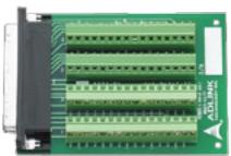
Terminal board TB-6201-01
Pin Assignment
CNI
| 22. COM0 | |
| 43. NO0 | 23. COM1 | 1. NC0 |
| 44. NO1 | 24. COM2 | 2. NCI |
| 45. NO2 | 25. COM3 | 3. NC2 |
| 46. NO3 | 26. COM4 | 4. NC3 |
| 47. NO4 | 27. COM5 | 5. NC4 |
| 48. NO5 | 28. COM6 | 6. NC5 |
| 49. NO6 | 29. COM7 | 7. NC6 |
| 50. NO7 | 30. COM8 | 8. NC7 |
| 51. NO8 | 31. COM9 | 9. NC8 |
| 52. NO | 32. COM10 | 10. NC9 |
| 53. NO10 | 33. COM11 | 11. NC10 |
| 54. NO11 | 34. COM12 | 12. NC11 |
| 55. NO12 | 35. COM13 | 13. NC12 |
| 56. NO13 | 36. COM14 | 14. NC13 |
| 57. NO14 | 37. COM15 | 15. NC14 |
| 58. NO15 | 38. N/C | 16. NC15 |
| 59. N/C | 39. N/C | 17. N/C |
| 60. AUX3 | 40. AUX4 | 18. AUX2/SHDNn |
| 61. AUX6 | 41. +5Vout | 19. AUX5 |
| 62. AUX7 | 42. AUX1/TRG_IN | 20. GND |
| 21. AUX0/S_ADV |
[🔗 Link to the original document](.pxi-7901-datasheet-20191223/pxi-7901-datasheet-20191223.pdf)