#

# Single Board Computer

# Reference Manual

P/N 50-1Z033-1000 Revision 1.0

# DISCLAIMER

ADLINK Technology, Incorporated makes no representations or warranties with respect to the contents of this manual or of the associated ADLINK products, and specifically disclaims any implied warranties of merchantability or fitness for any particular purpose. ADLINK shall under no circumstances be liable for incidental or consequential damages or related expenses resulting from the use of this product, even if it has been notified of the possibility of such damages. ADLINK reserves the right to revise this publication from time to time without obligation to notify any person of such revisions. If errors are found, please contact ADLINK at the address listed below this Disclaimer.

# TRADEMARKS

CoreModule and the Ampro logo are registered trademarks, and ADLINK, Little Board, LittleBoard, MightyBoard, MightySystem, MilSystem, MiniModule, ReadyBoard, ReadyBox, ReadyPanel, ReadySystem, RuffSystem are trademarks of ADLINK Technology, Inc. All other marks are the property of their respective companies.

REVISION HISTORY

<table><tr><td>Revision</td><td>Reason for Change</td><td>Date</td></tr><tr><td>A, A</td><td>Initial Release</td><td>Nov/07</td></tr><tr><td>A, B</td><td>Added header pinouts to hardware chapter</td><td>June/08</td></tr><tr><td>B, A</td><td>Added SATA interface; changed default of JP19 in table 2-3; revised RS-422/RS-485 info in ch 3; added PCI to ISA bridge section to ch 4</td><td>May/09</td></tr><tr><td>1.0</td><td>Revised Fig 3-2 pin numbering; removed all references to RS-422 from manual; revised the document part number to 50-1Z033-1000</td><td>Nov/09</td></tr><tr><td></td><td></td><td></td></tr><tr><td></td><td></td><td></td></tr><tr><td></td><td></td><td></td></tr></table>

ADLINK Technology, Incorporated

5215 Hellyer Avenue

San Jose, CA 95138-1007

Tel. 408 360-0200

Fax 408 360-0222

www.adlinktech.com

© Copyright 2007, 2008, 2009 ADLINK Technology, Incorporated

# Audience

This manual provides reference only for computer design engineers, including but not limited to hardware and software designers and applications engineers. ADLINK Technology, Inc. assumes you are qualified to design and implement prototype computer equipment.

# Contents

# Chapter 1 About This Manual ..

Purpose of this Manual ..

References ..

# Chapter 2 Product Overview...........

EBX Architecture... .3

Product Description.. .4

Board Features . .4

Block Diagram.. 7

Major Components (ICs).. ..8

Header Definitions ......... ....10

Jumper Header Definitions . ..13

Specifications......... ....13

Physical Specifications ..... ..13

Environmental Specifications.. ..14

Power Specifications ....... ..14

Thermal/Cooling Requirements.. ..14

# Chapter 3 Hardware . .17

Overview... .17

Interrupt Channel Assignments.. ...18

Memory Map . ..19

I/O Address Map . ...19

Floppy Drive Interface . ..20

Parallel Port Interface ..20

Serial Interfaces ..21

Utility Interfaces ..24

Utility 1 Interface . ..24

Keyboard Interface .. ..24

External Battery ... ..25

Reset Switch..... ..25

Speaker ....... ..25

Utility 2 Interface ..... .26

System Management Bus (SMBus) . ..26

Mouse, Power Button, and SMBus Interfaces.. ..26

Audio Interface . ..27

USB Interfaces........ ..28

USB 2.0 Support. ..28

Legacy USB Support . .28

Primary USB0 and USB1. ..28

Secondary USB2 and USB3.. ..29

Video Interfaces ...

CRT features: ..29

LVDS and TTL Flat Panel features: . ..29

TTL Flat Panel Interface ..30

LVDS Interface . .32

Miscellaneous .. ..33

User GPIO Signals ... ..33

Real-Time Clock (RTC) .34

Temperature Monitoring . 34

Oops! Jumper (BIOS Recovery) . . 34

Serial Console.... . 34

Serial Console Setup ... . 34

Hot (Serial) Cable . 34

Watchdog Timer... . 35

Power Interfaces .. 35

Power In . 35

Power On . . 36

Power-On Button . 36

# Chapter 4 BIOS Setup .......... .... 37

Introduction. . 37

Entering BIOS Setup (VGA Display) .. . 37

Entering BIOS Setup (Remote Access) . . 37

PCI-ISA Bridge Mapping .. .. 38

Logo Screen Utility (Splash Screen) . .. 39

Logo Screen Image Requirements . . 39

# Appendix A Technical Support . .. 41

# Index ..... ... 43

# List of Figures

Figure 2-1. Stacking PC/104 Modules with the LittleBoard 620 . 4

Figure 2-2. Functional Block Diagram .

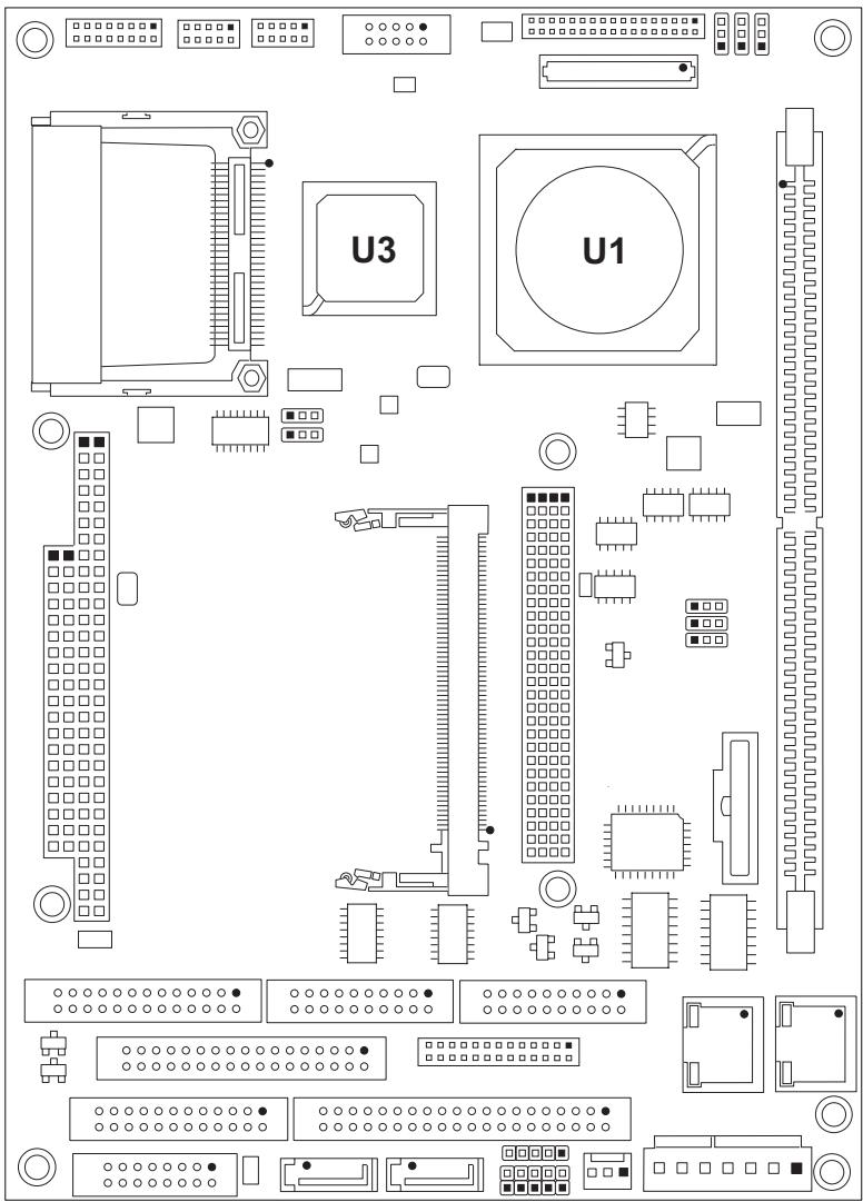
Figure 2-3. Component Location (Top view) ..... 9
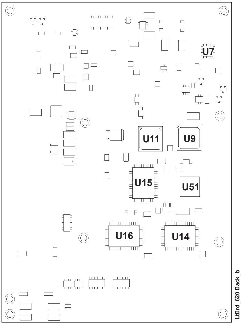
Figure 2-4. Component Locations (Bottom view) ....... .... 10

Figure 2-5. Header Pin Sequence Identification ......... .. 11

Figure 2-6. Header Locations (Top view) . . 12

Figure 2-7. LittleBoard 620 Dimensions (Top view) . .... 15

Figure 3-1. Oops! Jumper Connection.. . 34

Figure 3-2. Hot Cable Jumper .... . 34

# List of Tables

Table 2-1. Major Components Descriptions and Functions.. 8

Table 2-2. Header Descriptions ........ .... 10

Table 2-3. Jumper Settings ......... ..... 13

Table 2-4. Weight and Footprint Dimensions ...... .... 13

Table 2-5. Environmental Requirements . . 14

Table 2-6. Power Supply Requirements. . 14

Table 3-1. Interrupt Channel Assignments . . 18

Table 3-2. Memory Map .. . 19

Table 3-3. I/O Address Map ........ ..... 19

Table 3-4. Parallel Interface Pin/Signal Descriptions (J16) .... .. 20

Table 3-5. Serial A Interface Pin/Signal Descriptions (J12).. . 22

Table 3-6. Serial B Interface Pin/Signal Descriptions (J11).... . 23

Table 3-7. Utility 1 Interface Pin/Signal Descriptions (J15) .. . 25

Table 3-8. SMBus Reserved Addresses .... .. 26

Table 3-9. Utility 2 Interface Pin/Signal Descriptions (J13) .. . 26

Table 3-10. Audio Interface Pin/Signal Descriptions (J9) ..... . 27

Table 3-11. USB 0 & 1 Interface Pin/Signal Descriptions (J29A/B).. . 28

Table 3-12. USB 2 & 3 Interface Pin/Signal Descriptions (J30A/B) . ..29

Table 3-13. TTL Flat Panel Interface Pin/Signal Descriptions (J18) . ..30

Table 3-14. LVDS Interface Pin/Signal Descriptions (J26) . ..32

Table 3-15. User GPIO Signals Pin/Signal Descriptions (J14) . .33

Table 3-16. Power In Pin/Signal Descriptions (J19).... ...35

Table 3-17. Power On Pin/Signal Descriptions (J6).. ..36

Table 3-18. Power-On Button Interface Pin/Signal Descriptions (J32) . ..36

Table A-1. Technical Support Contact Information.. ..41

# Purpose of this Manual

This manual is for designers of systems based on the LittleBoard™ 620 single board computer (SBC). This manual contains information that permits designers to create an embedded system based on specific design requirements.

Information provided in this reference manual includes:

• LittleBoard 620 specifications
Environmental requirements
Major integrated circuits (chips) and features implemented
• LittleBoard 620 connector/pin numbers and definitions
• BIOS Setup information

Information not provided in this reference manual includes:

• Detailed chip specifications
• Internal component operation
• Internal registers or signal operations
Bus or signal timing for industry standard busses and signals

# References

The references in the following list may be helpful for you to complete your design successfully.

# Specifications:

EBX Spec Revision 2.0, March 1 2005
For the latest version of the EBX specifications, contact the PC/104 Consortium, at: Web site: http://www.pc104.org

• PC/104 Spec Revision 2.5, November 2003

• PC/104-Plus Spec Revision 2, November 2003

For latest revision of the PC/104 specifications, contact the PC/104 Consortium, at: Web site: http://www.pc104.org

• PCI 2.2 Compliant Specifications

For latest revision of the PCI specifications, contact the PCI Special Interest Group Office at: Web site: http://www.pcisig.com

Chip specifications used on the LittleBoard 620:

AMD, Inc., Geode LX 800 processor (with integrated Northbridge)
Web site:
http://www.amd.com/files/connectivitysolutions/geode/geode\_lx/33234F\_LX\_databook.pdf

• AMD, Inc. CS5536, used for the I/O Hub (Southbridge)

Web site:

http://www.amd.com/files/connectivitysolutions/geode/geode\_lx/33238G\_cs5536\_db.pdf

Intel Corporation and the 82551QM and 82551ER chips, used as Ethernet 1 and Ethernet 2 controllers, respectively.
Web site: http://www.intel.com/design/network/datashts/82551QM\_ds.htm
Web site: http://www.intel.com/design/network/datashts/82551ER\_ds.htm
• Winbond Electronics, Corp. and the W83627HG chip used as the Super I/O controller
Web site:
http://www.winbond-usa.com/products/winbond\_products/pdfs/PCIC/W83627HF\_F\_HG\_Ga.pdf
• Realtek and the ALC203-LF chip, used for the Audio CODEC.
Web site: http://www.realtek.com.tw/search/default.aspx?keyword=alc203
ITE Tech. Inc. and the IT8888G chip, used for the PCI-to-ISA bridge conversion.
Web site: http://www.ite.com.tw/EN/products\_more.aspx?CategoryID=3&ID=5,76

# NOTE

If you are unable to locate the datasheets using the links provided, copy the whole link into your web address bar and press enter. Otherwise, go to the manufacturer’s web site where you should be able to perform a search using the chip datasheet number or name listed, including the extension, htm, pdf, etc.

This introduction presents general information about the EBX architecture and the LittleBoard 620 single board computer (SBC). After reading this chapter you should understand:

EBX Architecture
LittleBoard 620 architecture
LittleBoard 620 features
• Major components
• Connectors
Jumper definitions

Specifications (physical, environmental, power, cooling)

# EBX Architecture

The “Embedded Board, eXpandable” (EBX) standard is the result of a collaboration between industry leaders, Motorola and Ampro, to unify the embedded computing industry on a full featured embedded single-board computer (SBC) standard. The EBX standard principally defines physical size, mounting hole pattern, and power connector locations. It does not specify processor type or electrical characteristics. There are recommended connector placements for serial/parallel, Ethernet, graphics, and memory expansion.

Derived from the LittleBoard form-factor originated in 1984, EBX combines a standard footprint with open interfaces. The EBX form-factor is small enough for deeply embedded applications, yet large enough to contain the functions of a fully embedded SBC (single board computer) including CPU, memory, mass storage interfaces, display controller, serial/parallel ports, today’s advanced operating systems, and other system functions. This embedded SBC standard ensures that embedded system OEMs can standardize their designs and that embedded computing solutions can be designed into space constrained environments with off-the-shelf components.

The EBX standard boasts highly flexible and adaptable system expansion, allowing easy and modular addition of functions such as additional USB 2.0 ports, Firewire or wireless networking not usually contained in standard product offerings. The EBX system expansion is based on popular existing industry standards, PC/104™ and PC/104-Plus™. PC/104 places the ISA bus on compact 3.6" x 3.8" modules with self-stacking capability. PC/104-Plus adds the power of a PCI bus to PC/104 while retaining the basic formfactor. Using PC/104 expansion cards, the PC/104 standard offers access to PC cards from the mobile and handheld computing markets.

The EBX standard integrates all these off-the-shelf standards into a highly embeddable SBC form-factor. EBX supports the legacy of PC/104, hosting the wide variety of embedded system oriented expansion modules from hundreds of companies worldwide. PC/104 brings the advantages of the latest portable and mobile system expansion technologies to embedded applications. See Figure 2-1 on page 4.

The EBX standard also brings stability to the embedded board market and offers OEMs assurance that a wide range of products will be available from multiple sources – now and in the future. The EBX standard is open to continuing technology advancements since it is processor independent. It creates opportunity for economies of scale in chassis, power supply, and peripheral devices.

The EBX specification is freely available to all interested. For further technical information on the EBX standard, go to the PC/104 Consortium web site at www.pc104.org.

![4-40 screws (4)\nPC/104 Module\n0.6 inch spacers (4)\nPC/104 Plus Module\nPCI Stackthrough Headers\n0.6 inch spacers (4)\nLittle Board 620\n4-40 nuts (4)\nISABus Stackthrough Expansion Headers\nLB620stackthru](.50-1z033-1000-lb620-rm-1-0/27f52842cae4b6bd4b0d84957953a994d955cda381f03061263393779616f02b.jpg)

Figure 2-1. Stacking PC/104 Modules with the LittleBoard 620

# Product Description

The LittleBoard 620 is an exceptionally high integration, high performance, rugged, and high quality singleboard system, which contains all the component subsystems of a PC motherboard plus the equivalent of up to 3 expansion boards. Based on the AMD Geode™ LX 800 processor, the LittleBoard 620 provides designers a complete, high performance embedded processor that conforms to the EBX V2.0 specification.

Each LittleBoard 620 incorporates an AMD Geode CS5536 chipset for the Graphics and Memory Hub (the Northbridge integrated in the CPU) and the I/O Hub (Southbridge) controllers. The Winbond Electronics Corp. Super I/O controller, W83627HF, adds I/O functions. Together, the AMD and Winbond chips provide four serial ports, a floppy and EPP/ECP parallel ports, four USB 2.0 ports, PS/2 keyboard and mouse interfaces, an Ultra/DMA 33/66 IDE controller supporting two IDE drives and one Compact Flash socket, a graphics controller, which provides CRT and LVDS/TTL flat panel video interfaces, and an audio AC’97 CODEC on the board. The LittleBoard 620 also supports two 10/100BaseT Ethernet interfaces, two SATA ports (DNP on certain models), and up to 1 GB of non-ECC DDR RAM in a single 184-pin DIMM socket. To provide the ISA bus on the board through the PC/104 connector, an ITE, IT8888G, PCI-to-ISA Bridge is included.

The LittleBoard 620 can be expanded through the PC/104 and PC/104-Plus expansion for additional system functions, as these buses offer compact, self-stacking, modular expandability. The PC/104 and PC/104-Plus buses are the embedded system version of the signal set provided on a desktop PC's ISA and PCI buses at 8MHz and 33MHz clock speeds, respectively.

Among the many embedded-PC enhancements on the LittleBoard 620 that ensure embedded system operation and application versatility are a Watchdog Timer, serial console support, battery-free boot, Compact Flash disk, and OEM logo customization (Splash Screen).

The LittleBoard 620 is particularly well suited to either embedded or portable applications and meets the size, power consumption, temperature range, quality, and reliability demands of embedded system applications. It can be stacked with ADLINK MiniModules™ or other PC/104-compliant expansion boards or it can be used as a powerful computing engine.

# Board Features

CPU features

♦ Provides a 500 MHz AMD Geode LX800 processor
64-bit DDR memory interface up to 400 MHZ

• Memory

Single standard 184-pin DDR DIMM slot

Supports +2.5V DDR RAM up to 1GB
Supports up to PC2700 DDR 333

PC/104-Plus Bus Interfaces

♦ PCI Bus at 33MHz
♦ PCI 2.2 compliant signals
♦ PC/104 (ISA) Bus at 8MHz

Serial ATA Interface (SATA) - [DNP on certain models]

♦ Provides two 7-pin SATA ports
♦ Provides 1.5 Gb/second data transfer rate

IDE Interfaces

♦ Provides one enhanced IDE controller
Supports dual bus master mode
Supports Ultra DMA 33/66/100 modes
Supports ATAPI and DVD peripherals
Supports IDE native and ATA compatibility modes
♦ Provides Compact Flash socket (on Primary IDE bus with Master/Slave jumper)

Floppy Disk Interface

Supports one standard floppy disk drive interface
Supports all standard PC/AT formats: 360KB, 1.2MB, 720KB, 1.44MB, 2.88MB

• Parallel Port

Provides a standard printer interface
Supports IEEE standard 1284 protocols of EPP and ECP outputs
Supports Bi-directional data lines
Supports 16 byte FIFO for ECP mode

Serial Ports

♦ Provides four buffered serial ports with full handshaking
♦ Provides 16550-equivalent controllers, each with a built-in 16-byte FIFO buffer
Supports full modem capability on all four ports
Supports RS232 operation on each port
Supports RS232 or RS485 operation on two ports (COM1 and COM2)
Supports programmable word length, stop bits, and parity
Supports 16-bit programmable baud-rate generator and an interrupt generator

USB Ports

♦ Provides two root USB hubs
Provides up to four USB ports
Supports USB boot devices
Supports USB v2.0 EHCI and v1.1 OHCI
Supports over-current detection status

Keyboard/Mouse Interface

♦ Provides PS/2 keyboard interface
♦ Provides PS/2 mouse interface

Audio interface

♦ Provides AC’97 CODEC on board
Supports AC’97 2.3 standard

Ethernet Interface

♦ Provides two fully independent Ethernet ports
♦ Provides integrated LEDs on each port (Link/Activity and Speed)
♦ Provides Intel 82551ER and 82551QM controller chips
Supports IEEE 802.3 10/100BaseTX compatible physical layers
Supports Auto-negotiation for speed, duplex mode, and flow control
Supports full-duplex or half-duplex mode

Full-duplex mode supports transmit and receive frames simultaneously
Supports IEEE 802.3x Flow control in full duplex mode
Half-duplex mode supports enhanced proprietary collision reduction mode

Video Interfaces (CRT/TTL/LVDS)

♦ Support CRT (1920 x 1440 at 85Hz and 1600 x 1200 at 100 Hz) with up to 254MB UMA (Unified Memory Architecture)
♦ Provide 10-pin VGA header
Provide TTL, 24-bit, flat panel outputs pared with resolution up to 1600 x 1200
♦ Provide LVDS flat panel outputs (single channel, five differential signals) on 30-pin header

Miscellaneous

♦ Real-Time Clock (RTC) with replaceable battery
Battery-free boot (Boots even if battery is dead or missing)
♦ Supports both on-board or external battery for Real-Time Clock operation
Thermal and Voltage monitoring
♦ Oops! Jumper (BIOS recovery) support
Serial Console
Watchdog Timer (WDT)
USB Boot
♦ LAN Boot (PXE)

# Block Diagram

Figure 2-2 shows the functional components of the board.
![The diagram illustrates a motherboard architecture centered around a CPU and an I/O Hub. Here are the labeled blocks and their connections:\n\n**Central Components**\n*   **AMD Geode, LX800 CPU (Integrated Northbridge)**\n*   **I/O Hub CS5536 (Southbridge)**\n\n**CPU Connections**\n*   Connected bidirectionally to **DDR1 DIMM**.\n*   Connected via a line labeled **Video** to **TFT Connector**, **CRT Connector**, and **LVDS Transmitter**.\n*   **LVDS Transmitter** connects bidirectionally to **LVDS Connector**.\n*   Connected via **PCI Bus** to the **I/O Hub CS5536 (Southbridge)** and to the left-side peripherals.\n\n**PCI Bus Peripherals (Left Side)**\n*   **Mini PCI Connector**\n*   **PC/104-Plus Connector**\n*   **SATA Controller (DNP on certain models)** connects to **SATA Connectors (2) - (DNP on certain models)**.\n\n**PCI Bus Peripherals (Right Side)**\n*   **Ethernet Controller 82551QM** connects to **Magnetics-RJ45**.\n*   **Ethernet Controller 82551ER** connects to **Magnetics-RJ45**.\n*   **PCI -to-ISA Bridge IT8888G-L** connects to **PC/104 Connector**.\n\n**I/O Hub Connections**\n*   Connected via **AC'97 Link** to **AC'97 CODEC ALC203-LF**, which connects to **Audio Header**.\n*   Connected via **USB 2.0** to **USB Headers (4)**.\n*   Connected via **IDE Channel** to **Compact Flash Socket**.\n*   Connected via **PATA** to **IDE Connector**.\n*   Connected via **LPC Bus** to the bottom section components.\n\n**LPC Bus Section**\nThe **LPC Bus** connects to three blocks:\n1.  **Super I/O - 1 W83627HG**\n2.  **Super I/O - 2 W83627HG**\n3.  **ROM BIOS SST49LF004B FWH**\n\n**Super I/O - 1 W83627HG**\n*   Connects bidirectionally to **RS232/485 Transceiver**, which connects to **COM 1 & 2 Header (RS232/485)**.\n*   Connects bidirectionally to **Floppy Drive Header**, **Parallel Port Header**, and **Keyboard/Mouse Header**.\n\n**Super I/O - 2 W83627HG**\n*   Connects bidirectionally to **GPIO Header (User Defined)**.\n*   Connects bidirectionally to **RS232 Transceiver**, which connects to **COM 3 & 4 Header (RS232)**.](.50-1z033-1000-lb620-rm-1-0/331e53a5459a9557ac239a83f616f256492b9660b933803d6b5632fa0a569eb2.jpg)

Figure 2-2. Functional Block Diagram

# Major Components (ICs)

Table 2-1 lists the major ICs, including a brief description of each, on the LittleBoard 620. Figures 2-3 and 2-4 show the locations of the ICs.

Table 2-1. Major Components Descriptions and Functions

<table><tr><td>Chip Type</td><td>Mfg.</td><td>Model</td><td>Description</td><td>Function</td></tr><tr><td>CPU (U1)</td><td>AMD</td><td>Geode LX800</td><td>500 MHz CPU</td><td>Memory and video</td></tr><tr><td>I/O Hub (U3)</td><td>AMD</td><td>CS5536</td><td>Southbridge functions (provides some of standard I/O functions)</td><td>I/O Functions</td></tr><tr><td>Audio (U7)</td><td>Realtek</td><td>ALC203-LF</td><td>Audio &#x27;97 CODEC for Audio In/ Out signals</td><td>Audio In/Out</td></tr><tr><td>Super I/O 1 (U14) [See Figure 2-4]</td><td>Winbond Electronics, Corp.</td><td>W83627HG</td><td>Super I/O controller (provides Floppy, Parallel, Keyboard, and Mouse)</td><td>I/O Functions</td></tr><tr><td>Super I/O 2 (U16) [See Figure 2-4]</td><td>Winbond Electronics, Corp.</td><td>W83627HG</td><td>Super I/O controller (provides GPIO and RS232 transceiver)</td><td>I/O Functions</td></tr><tr><td>Ethernet 1 Controller (U9) [See Figure 2-4]</td><td>Intel</td><td>82551QM</td><td>Ethernet chip (provide two independent 10/100BaseT based network channels)</td><td>Ethernet functions</td></tr><tr><td>Ethernet 2 Controller (U11) [See Figure 2-4]</td><td>Intel</td><td>82551ER</td><td>Ethernet chip (provide two independent 10/100BaseT based network channels)</td><td>Ethernet functions</td></tr><tr><td>SATA Controller (U15) [See Figure 2-4 - DNP on certain models]</td><td>VIA</td><td>VT6421L</td><td>PCI-to-SATA control</td><td>I/O functions</td></tr><tr><td>ISA Bridge (U51) [See Figure 2-4]</td><td>ITE</td><td>IT8888G-L</td><td>PCI-to-ISA bridge conversion</td><td>ISA Bus</td></tr></table>

![Top-down schematic of a computer motherboard showing various electronic components and connectors (no text or labels)](.50-1z033-1000-lb620-rm-1-0/41f6ffb2039fa558afb8cb5907850d0d3e8ae70e8b2af8439c6dea06de1529c7.jpg)

LB620Cmpnts\_top\_b
Figure 2-3. Component Location (Top view)

![U7\nU11 U9\nU15 U51\nU16 U14\nLtBrd_620 Back_b](.50-1z033-1000-lb620-rm-1-0/90d5b528b868674a90f4f305417bdf6eb3547707b6aec01012c8500fe8d52768.jpg)

Figure 2-4. Component Locations (Bottom view)

# Header Definitions

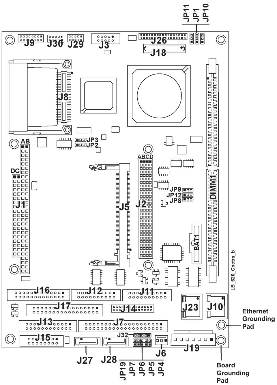
Table 2-2 describes the headers shown in Figure 2-6 on page 12. All I/O headers use 0.100" (2.54mm) pitch unless otherwise indicated. All standard headers and connectors do not indicate pitch.

Table 2-2. Header Descriptions

<table><tr><td>Jack #</td><td>Name</td><td>Description</td></tr><tr><td>BAT1</td><td>Battery Socket</td><td>Battery socket for 3 volt Lithium battery</td></tr><tr><td>DIMM1</td><td>Memory</td><td>184-pin, 0.050" (1.27mm), slot for a single DDR RAM DIMM</td></tr><tr><td>J1A,B,C,D</td><td>PC/104</td><td>104-pin, standard connector for ISA bus</td></tr><tr><td>J2A,B,C,D</td><td>PC/104-Plus</td><td>120-pin, standard connector for PCI bus</td></tr><tr><td>J3</td><td>CRT Video</td><td>10-pin header for output to a CRT type monitor</td></tr><tr><td>J5</td><td>Mini PCI</td><td>124-pin, 0.032" (0.80mm) connector for mini PCI cards</td></tr><tr><td>J6</td><td>Power On</td><td>3-pin header for ATX Power On functions</td></tr><tr><td>J7</td><td>IDE header</td><td>40-pin header for the IDE interface</td></tr><tr><td>J8</td><td>Compact Flash</td><td>50-pin, 0.050" (1.27mm), socket accepts Type 1 or Type II Compact Flash cards</td></tr><tr><td>J9</td><td>Audio In/Out</td><td>16-pin, 0.079" (2mm), header for all of the audio signals (input/output)</td></tr><tr><td>J10</td><td>LAN 2</td><td>8-pin RJ45 connector for 10/100BaseT Ethernet port</td></tr><tr><td>J11</td><td>Serial B</td><td>20-pin, header for serial ports 3 and 4 (COM 3 &amp; COM 4)</td></tr><tr><td>J12</td><td>Serial A</td><td>20-pin, header for serial ports 1 and 2 (COM 1 &amp; COM 2)</td></tr><tr><td>J13</td><td>Utility 2</td><td>24-pin header for mouse and SMBus</td></tr><tr><td>J14</td><td>GPIO</td><td>26-pin, 0.079" (2mm) header for general purpose I/O signals</td></tr><tr><td>J15</td><td>Utility 1</td><td>16-pin header for keyboard, external battery, reset switch, speaker</td></tr><tr><td>J16</td><td>Parallel</td><td>26-pin header for parallel port</td></tr><tr><td>J17</td><td>Floppy</td><td>34-pin header for floppy disk drive interface</td></tr><tr><td>J18</td><td>TTL Video</td><td>50-pin, 0.039" (1mm) header for TTL video displays</td></tr><tr><td>J19</td><td>Power In</td><td>7-pin, 0.156" (3.96mm) header for input power</td></tr><tr><td>J23</td><td>LAN 1</td><td>8-pin, standard RJ45 connector for 10/100BaseT Ethernet port</td></tr><tr><td>J26</td><td>LVDS Video</td><td>30-pin, 0.079" (2mm), header for LVDS video displays</td></tr><tr><td>J27</td><td>SATA1</td><td>7-pin, standard connector for serial ATA - [DNP on certain models]</td></tr><tr><td>J28</td><td>SATA2</td><td>7-pin, standard connector for serial ATA - [DNP on certain models]</td></tr><tr><td>J29</td><td>USB</td><td>10-pin, 0.079" (2mm) header for USB 1 and USB 2 ports</td></tr><tr><td>J30</td><td>USB</td><td>10-pin, 0.079" (2mm) header for USB 3 and USB 4 ports</td></tr><tr><td>J32</td><td>Reset and Power-On</td><td>5-pin header for reset switch and power-on button</td></tr></table>

# NOTE

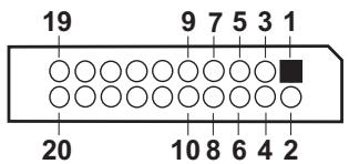
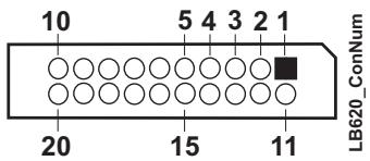
The pinout tables in Chapter 3 of this manual identify pin sequence using the following methods: A 20-pin header with two rows of pins, using odd/even numbering, where pin 2 is directly across from pin 1, is noted as 20-pin, 2 rows, odd/even (1, 2). Alternately, a 20-pin connector using consecutive numbering, where pin 11 is directly across from pin 1, is noted in this way: 20-pin, 2 rows, consecutive (1, 11). The second number in the parenthesis is always directly across from pin-1. See Figure 2-5.

20-pin, two rows, Odd/Even, (1, 2)
![19\n9 7 5 3 1\n20 10 8 6 4 2](.50-1z033-1000-lb620-rm-1-0/32c5427d81ca7742c5f0ea6caba5af14ecc11d47e7fda6813bccc108c98fff28.jpg)

Or

20-pin, two rows, Consecutive, (1, 11)
![| Position | Value |\n|---|---|\n| 10 | 10 |\n| 5 | 5 |\n| 4 | 4 |\n| 3 | 3 |\n| 2 | 2 |\n| 1 | 1 |\nLB620_ConNum\n| \n| \n| \n| \n| \n| \n| \n| \n| \n| \n| \n| \n| \n| \n| \n| \n| \n| \n| \n| \n| \n| \n| \n| \n| \n| \n| \n| \n| \n| \n| \n| \n| \n| \n| \n| \n| \n| \n| \n| \n| \n| \n| \n| \n| \n| \n| \n| \n| \n| \n| |\n| 20 | |\n| 15 | |\n| 11 | |](.50-1z033-1000-lb620-rm-1-0/b97e723690588e0b98321ed63b61aeb6809e5324ff9f39bcf7d8a3a0b1341f22.jpg)

Figure 2-5. Header Pin Sequence Identification
![JP11\nJP1\nJP10\nJ9 J30 J29 J3 J26\nJ18\nJ8\nJP3\nJP2\nAB\nDC\nJ1\nJ5 ABCD\nJ2 JP9 JP12 JP8\nBAT1 DIMM1\nLB_620_Cnctrs_b\nJ16 J12 J11\nJ17 J14\nJ13 J7 J23 J10\nJ15 J32\nJ27 J28 J6 Board\nJP19 JP7 JP6 JP5 JP4 Grounding Pad](.50-1z033-1000-lb620-rm-1-0/6c355957b5f197003de2fd2224e3ff07aba711ded9e7b722c52fc2eb711ab8f3.jpg)

Figure 2-6. Header Locations (Top view)

# CAUTION

The two Ethernet ports share a common ground (transformer center tap), that is floating until you determine how the common ground is connected. The grounding holes (8) of the LittleBoard 620 are connected to ground potential (return) of the DC power supply connected to the board through J19.

# NOTE

Pin-1 is shown as a black pin (square or round) on all connectors and headers in all illustrations.

# Jumper Header Definitions

Table 2-3 describes the jumper headers shown in Figure 2-6.

Table 2-3. Jumper Settings

<table><tr><td>Jumper #</td><td>Installed</td><td>Removed/Installed</td></tr><tr><td>JP1 – LVDS PWR SEL</td><td>Enable +3.3V (pins 1-2) Default</td><td>Enable +5V (pins 2-3)</td></tr><tr><td>JP2 – Compact Flash Master/Slave</td><td>Enable Slave (pins 1-2)</td><td>Enable Master (pins 2-3) Default</td></tr><tr><td>JP3 – Compact Flash Voltage Selection</td><td>Enable +5V (pins 1-2)</td><td>Enable +3.3V (pins 2-3) Default</td></tr><tr><td>JP4 – Serial Port 1 RS485 Termination</td><td>Enable Termination (pins 1-2) [SER0 Data P]</td><td>Disable Termination (Removed) Default - RS232</td></tr><tr><td>JP5 – Serial Port 2 RS485 Termination</td><td>Enable Termination (pins 1-2) [SER1 Data N]</td><td>Disable Termination (Removed) Default - RS232</td></tr><tr><td>JP6 – Serial Port 1 RS485 Termination</td><td>Enable Termination (pins 1-2) [SER0 Data N]</td><td>Disable Termination (Removed) Default - RS232</td></tr><tr><td>JP7 – Serial Port 2 RS485 Termination</td><td>Enable Termination (pins 1-2) [SER1 Data P]</td><td>Disable Termination (Removed) Default - RS232</td></tr><tr><td>JP8 – Oops jumper</td><td>Normal (pins 1-2) Default</td><td>Clear CMOS (pins 2-3)</td></tr><tr><td>JP9 – PCI REQ SEL</td><td>Mini PCI (pins 1-2) Default</td><td>PC/104-Plus (pins 2-3)</td></tr><tr><td>JP10 – TTL PWR SEL</td><td>Enable +3.3V (pins 1-2) Default</td><td>Enable +5V (pins 2-3)</td></tr><tr><td>JP11 – TTL BKLT SEL</td><td>Enable +5V (pins 1-2) Default</td><td>Enable +12V (pins 2-3)</td></tr><tr><td>JP12 – PCI GNT SEL</td><td>Mini PCI (pins 1-2) Default</td><td>PC/104-Plus (pins 2-3)</td></tr><tr><td>JP19 – AT Power Button</td><td>Enable AT Power (pins 1-2)</td><td>Enable ATX Power (Removed) Default</td></tr></table>

NOTE Only the jumper headers listed above are populated on the board. All listed jumper headers use 0.079" (2mm) pitch. A jumper that is removed may be placed on one of the jumper pins for safe keeping.

# Specifications

# Physical Specifications

Table 2-4 gives the physical dimensions of the board.

Table 2-4. Weight and Footprint Dimensions

<table><tr><td>Item</td><td>Dimension</td><td rowspan="6">NOTE</td><td rowspan="6">Overall height is measured from the upper board surface to the highest permanent component (battery in socket) on the upper board surface. This measurement does not include the various heatsinks or various size DIMMs inserted into the socket. The DIMMs or heatsinks could increase this dimension.</td></tr><tr><td>Weight</td><td>0.28kg (0.61 lb)</td></tr><tr><td>Height (overall)</td><td>24.94mm (0.982&quot;)</td></tr><tr><td>Width</td><td>146mm (5.75&quot;)</td></tr><tr><td>Length</td><td>203mm (8.0&quot;)</td></tr><tr><td>Thickness</td><td>2.36mm (0.093&quot;)</td></tr></table>

# Environmental Specifications

Table 2-5 provides the most efficient operating and storage condition ranges required for this board.

Table 2-5. Environmental Requirements

<table><tr><td></td><td>Parameter</td><td>500MHz Geode LX 800 Conditions</td></tr><tr><td rowspan="3">Temperature</td><td>Operating</td><td>-20° to +70°C (-4° to +158°F)</td></tr><tr><td>Extended (Optional)</td><td>-40° to +85°C (-40° to +185°F)</td></tr><tr><td>Storage</td><td>-55° to +85°C (-67° to +185°F)</td></tr><tr><td rowspan="2">Humidity</td><td>Operating</td><td>5% to 90% relative humidity, non-condensing</td></tr><tr><td>Non-operating</td><td>5% to 95% relative humidity, non-condensing</td></tr></table>

# Power Specifications

Table 2-6 shows the power requirements for the LittleBoard 620.

Table 2-6. Power Supply Requirements

<table><tr><td>Parameter</td><td>500MHz Geode LX 800 Characteristics</td></tr><tr><td>Input Type</td><td>Regulated DC voltages</td></tr><tr><td>In-rush Current (Typical)</td><td>7.16A (35.80W)</td></tr><tr><td>Idle Power (Typical)</td><td>1.57A (7.87W)</td></tr><tr><td>BIT* Current (Typical)</td><td>2.17A (10.85W)</td></tr></table>

# Operating configurations:

In-rush operating configuration includes video and 512MB DDR RAM.
Idle operating configuration includes the In-rush configuration as well as an I/O board, one IDE hard drive with Windows XP SP2, floppy, keyboard, and mouse.
\*BIT = Burn-In-Test. Operating configuration includes idle configuration as well as four serial loopbacks, one parallel loop-back, one USB Jump Drive, one on-board Compact Flash drive with 64MB Compact Flash, two Ethernet connections, two USB Compact Flash readers with 64MB Compact Flash, one external-power USB CD-ROM.

# Thermal/Cooling Requirements

The LittleBoard 620 is designed to operate at the maximum speed of the 500 MHz CPU without heatsinks or fans.

# Mechanical Specifications

Figure 2-7 shows the top view of the LittleBoard 620 with the mechanical mounting dimensions.
![0.20\n0\n2.65\n5.80\nLB_620_Dmn_b\n7.22\n7.60\n7.80\n0.20\n0\n5.35\n5.55](.50-1z033-1000-lb620-rm-1-0/338b3327d769e296550c4374b18c277f0498ed273321263239d0d39ae9018a24.jpg)

Figure 2-7. LittleBoard 620 Dimensions (Top view)

NOTE All dimensions are given in inches.

# Overview

This chapter discusses the following features of the connectors:

Interrupt Channel Assignments
• Memory Map
• I/O Address Map
Floppy Interface
. Serial Interfaces
. Parallel Interface
Utility Interfaces
♦ Keyboard
♦ Mouse
♦ Battery
♦ Reset Switch
♦ Speaker
♦ SMBus

Audio Interface
. USB Interfaces
• CRT/TTL/LVDS Video Interfaces
Miscellaneous

♦ User GPIO Signals
Time of Day/RTC
Temperature Monitoring
♦ Oops! Jumper (BIOS recovery)
♦ Serial Console
Watchdog Timer

. Power Interface

# NOTE

ADLINK Technology, Inc. only supports the features/options tested and listed in this manual. The main integrated circuits (chips) used in the LittleBoard 620 may provide more features or options than are listed for the LittleBoard 620, but some of these chip features/options are not supported on the board and may not function as specified in the chip documentation.

This chapter does not include pinout tables for standard headers and connectors such as PC/104, PC/104-Plus, Ethernet RJ45, 40-pin IDE, SATA, and Compact Flash.

# Interrupt Channel Assignments

The interrupt channel assignments are shown in Table 3-1.

Table 3-1. Interrupt Channel Assignments

<table><tr><td>Device vs IRQ No.</td><td>0</td><td>1</td><td>2</td><td>3</td><td>4</td><td>5</td><td>6</td><td>7</td><td>8</td><td>9</td><td>10</td><td>11</td><td>12</td><td>13</td><td>14</td><td>15</td></tr><tr><td>Timer</td><td>X</td><td></td><td></td><td></td><td></td><td></td><td></td><td></td><td></td><td></td><td></td><td></td><td></td><td></td><td></td><td></td></tr><tr><td>Keyboard</td><td></td><td>X</td><td></td><td></td><td></td><td></td><td></td><td></td><td></td><td></td><td></td><td></td><td></td><td></td><td></td><td></td></tr><tr><td>Secondary Cascade</td><td></td><td></td><td>X</td><td></td><td></td><td></td><td></td><td></td><td></td><td></td><td></td><td></td><td></td><td></td><td></td><td></td></tr><tr><td>COM1</td><td></td><td></td><td></td><td>O</td><td>D</td><td></td><td></td><td></td><td></td><td></td><td></td><td></td><td></td><td></td><td></td><td></td></tr><tr><td>COM2</td><td></td><td></td><td></td><td>D</td><td>O</td><td></td><td></td><td></td><td></td><td></td><td></td><td></td><td></td><td></td><td></td><td></td></tr><tr><td>COM3</td><td></td><td></td><td></td><td></td><td>O</td><td></td><td></td><td></td><td></td><td>O</td><td>O</td><td>D</td><td></td><td></td><td></td><td></td></tr><tr><td>COM4</td><td></td><td></td><td></td><td>O</td><td></td><td></td><td></td><td></td><td></td><td>O</td><td>D</td><td>O</td><td></td><td></td><td></td><td></td></tr><tr><td>Floppy</td><td></td><td></td><td></td><td></td><td></td><td></td><td>D</td><td></td><td></td><td></td><td></td><td></td><td></td><td></td><td></td><td></td></tr><tr><td>Parallel</td><td></td><td></td><td></td><td></td><td></td><td>O</td><td></td><td>D</td><td></td><td></td><td></td><td></td><td></td><td></td><td></td><td></td></tr><tr><td>RTC</td><td></td><td></td><td></td><td></td><td></td><td></td><td></td><td></td><td>X</td><td></td><td></td><td></td><td></td><td></td><td></td><td></td></tr><tr><td>IDE Primary</td><td></td><td></td><td></td><td></td><td></td><td></td><td></td><td></td><td></td><td></td><td></td><td></td><td></td><td></td><td>D</td><td>O</td></tr><tr><td>Math Coprocessor</td><td></td><td></td><td></td><td></td><td></td><td></td><td></td><td></td><td></td><td></td><td></td><td></td><td></td><td>X</td><td></td><td></td></tr><tr><td>PS/2 Mouse</td><td></td><td></td><td></td><td></td><td></td><td></td><td></td><td></td><td></td><td></td><td></td><td></td><td>X</td><td></td><td></td><td></td></tr><tr><td>PCI INTA</td><td colspan="16">Automatically Assigned</td></tr><tr><td>PCI INTB</td><td colspan="16">Automatically Assigned</td></tr><tr><td>PCI INTC</td><td colspan="16">Automatically Assigned</td></tr><tr><td>PCI INTD</td><td colspan="16">Automatically Assigned</td></tr><tr><td>USB</td><td colspan="16">Automatically Assigned</td></tr><tr><td>VGA</td><td colspan="16">Automatically Assigned</td></tr><tr><td>Ethernet</td><td colspan="16">Automatically Assigned</td></tr></table>

Legend: D = Default, O = Optional, X = Fixed

NOTE The IRQs for the Ethernet, Video, USB, and PCI are automatically assigned by the BIOS Plug and Play logic. Local IRQs assigned during initialization can not be used by external devices.

# Memory Map

Table 3-2 provides the common PC/AT memory allocations. Memory below 000500h is used by the BIOS.

Table 3-2. Memory Map

<table><tr><td colspan="2">Base Address</td><td>Function</td></tr><tr><td>00000000h</td><td>- 0009FFFFh</td><td>Conventional Memory</td></tr><tr><td>000A0000h</td><td>- 000AFFFFh</td><td>Graphics Memory</td></tr><tr><td>000B0000h</td><td>- 000B7FFFh</td><td>Mono Text Memory</td></tr><tr><td>000B8000h</td><td>- 000BFFFFh</td><td>Color Text Memory</td></tr><tr><td>000C0000h</td><td>- 000C7FFFh</td><td>Standard Video BIOS</td></tr><tr><td>000D0000h</td><td>- 000DFFFFh</td><td>Reserved for Extended BIOS</td></tr><tr><td>000E0000h</td><td>- 000FFFFFFh</td><td>System BIOS Area (Storage and RAM Shadowing)</td></tr><tr><td>00100000h</td><td>- Top of DRAM</td><td>Extended Memory (If on-board VGA is enabled, then the amount of memory assigned is subtracted from extended memory.)</td></tr><tr><td>FFF80000h</td><td>- FFFFFFFh</td><td>System Flash</td></tr></table>

# I/O Address Map

Table 3-3 shows the I/O address map.

Table 3-3. I/O Address Map

<table><tr><td>Address (hex)</td><td>Subsystem</td></tr><tr><td>000-00F</td><td>Primary DMA Controller</td></tr><tr><td>020-021</td><td>Master Interrupt Controller</td></tr><tr><td>040-043</td><td>Programmable Interrupt Timer (Clock/Timer)</td></tr><tr><td>060-06F</td><td>Keyboard Controller</td></tr><tr><td>070-07F</td><td>CMOS RAM, NMI Mask Reg, RT Clock</td></tr><tr><td>080-09F</td><td>DMA Page Registers</td></tr><tr><td>102</td><td>Video subsystem register</td></tr><tr><td>0A0-0BF</td><td>Slave Interrupt Controller</td></tr><tr><td>0C0-0DF</td><td>Slave DMA Controller #2</td></tr><tr><td>0F0-0FF</td><td>Math Coprocessor</td></tr><tr><td>1F0-1F8</td><td>IDE Hard Disk Controller</td></tr><tr><td>201</td><td>Watchdog Timer (WDT)</td></tr><tr><td>278-27F</td><td>Parallel Printer</td></tr><tr><td>2E8-2FF</td><td>Serial Port 4 (COM4)</td></tr><tr><td>2F8-2FF</td><td>Serial Port 2 (COM2)</td></tr><tr><td>378-37F</td><td>Parallel Port (Standard and EPP)</td></tr><tr><td>3C0-3DF</td><td>VGA</td></tr><tr><td>3E8-3EF</td><td>Serial Port 3 (COM3)</td></tr><tr><td>3F0-3F7</td><td>Floppy Disk Controller</td></tr><tr><td>3F8-3FF</td><td>Serial Port 1 (COM1)</td></tr><tr><td>778-77A</td><td>Parallel Port (ECP Extensions) (Port 378+400)</td></tr><tr><td>A79</td><td>ISA PnP Ports</td></tr><tr><td>CF8-CFF</td><td>PCI bus Configuration Address and Data</td></tr></table>

# Floppy Drive Interface

The Super I/O - 1 controller (W83627HF) provides the floppy controller and supports one floppy drive. The floppy signals are provided through the standard 34-pin header (J17). The floppy controller will support a 360k, 720k, 1.2M, 1.44M, or 2.88M drive.

The floppy drive connector has 34 pins, 2 rows, odd/even, (1, 2) with 0.100" (2.54mm) pitch.

# Parallel Port Interface

Parallel port supports standard parallel, Bi-directional, ECP and EPP protocols. The Super I/O - 1 controller (W83627HF) provides the parallel port interface.

The parallel header has 26 pins, 2 rows, odd/even, (1, 2), with 0.100" (2.54mm) pitch.

Table 3-4. Parallel Interface Pin/Signal Descriptions (J16)

<table><tr><td>Pin #</td><td>Signal</td><td>In/Out</td><td>Description</td></tr><tr><td>1</td><td>Strobe*</td><td>Out</td><td>Strobe* – This is an output signal used to strobe data into the printer. I/O pin in ECP/EPP mode.</td></tr><tr><td>2</td><td>AFD*</td><td>Out</td><td>Auto Feed* – This is a request signal into the printer to automatically feed one line after each line is printed.</td></tr><tr><td>3</td><td>PD0</td><td>I/O</td><td>Parallel Port Data 0 – These pins (0 to 7) provide parallel port data.</td></tr><tr><td>4</td><td>ERR*</td><td>Out</td><td>Error* – This is a status output signal from the printer. A Low State indicates an error condition on the printer.</td></tr><tr><td>5</td><td>PD1</td><td>I/O</td><td>Parallel Port Data 1 – Refer to pin-3 for more information.</td></tr><tr><td>6</td><td>INIT*</td><td>Out</td><td>Initialize* – This signal used to Initialize printer. Output in standard mode, I/O in ECP/EPP mode.</td></tr><tr><td>7</td><td>PD2</td><td>I/O</td><td>Parallel Port Data 2 – Refer to pin-3 for more information.</td></tr><tr><td>8</td><td>SLIN</td><td>Out</td><td>Select In – This output signal is used to select the printer. I/O pin in ECP/EPP mode.</td></tr><tr><td>9</td><td>PD3</td><td>I/O</td><td>Parallel Port Data 3 – Refer to pin-3 for more information.</td></tr><tr><td>10, 12</td><td>GND</td><td></td><td>Ground</td></tr><tr><td>11</td><td>PD4</td><td>I/O</td><td>Parallel Port Data 4 – Refer to pin-3 for more information.</td></tr><tr><td>13</td><td>PD5</td><td>I/O</td><td>Parallel Port Data 5 – Refer to pin-3 for more information.</td></tr><tr><td>14, 16</td><td>GND</td><td></td><td>Ground</td></tr><tr><td>15</td><td>PD6</td><td>I/O</td><td>Parallel Port Data 6 – Refer to pin-3 for more information.</td></tr><tr><td>17</td><td>PD7</td><td>I/O</td><td>Parallel Port Data 7 – Refer to pin-3 for more information.</td></tr><tr><td>18, 20</td><td>GND</td><td></td><td>Ground</td></tr><tr><td>19</td><td>ACK*</td><td>In</td><td>Acknowledge* – This printer output status indicates it has received the data and is ready to accept new data if the signal state is Low.</td></tr><tr><td>21</td><td>BUSY</td><td>In</td><td>Busy – This printer output status indicates the printer is not ready to accept data if the signal state is High.</td></tr><tr><td>22, 24</td><td>GND</td><td></td><td>Ground</td></tr><tr><td>23</td><td>PE</td><td>In</td><td>Paper End – The printer output status indicates the printer is out of paper if the signal state is High.</td></tr></table>

Table 3-4. Parallel Interface Pin/Signal Descriptions (J16)

<table><tr><td>25</td><td>SLCT</td><td>In</td><td>Select – This printer output status indicates the printer is selected and powered on if the signal state is high.</td></tr><tr><td>26</td><td>Key/NC</td><td></td><td>Key - Not connected</td></tr></table>

Note: The shaded area denotes power or ground. The signals marked with \* = Negative true logic.

# Serial Interfaces

The LittleBoard 620 supports 4 independent serial ports, using two separate chips. The Super I/O - 1 controller (W83627HG) provides serial ports 1 and 2 through the Serial A header (J12) and the Super I/O - 2 controller (W83627HG) provides serial ports 3 and 4 through Serial B header (J11). The four serial ports support the following features:

• Auto Direction Control for RS485
Four individual 16550-compatible UARTs
Programmable word length, stop bits and parity
16-bit programmable baud rate generator
Interrupt generator
Loop-back mode
Four individual 16-bit FIFOs
Serial A Interface (J12)

♦ Serial Port 1 (COM1) supports RS232 full modem and RS485 half duplex (2-wire)

♦ Serial Port 2 (COM2) supports RS232 full modem and RS485 half duplex (2-wire)

# NOTE

The RS232 and RS485 modes are selected for Serial A in the BIOS Setup Utility under the submenu, Super I/O Configuration in the Advanced menu screen for Serial ports 1 (COM1) and 2 (COM2). However, the RS232 mode is the default (Standard) for any serial port.

RS485 mode termination must also be set using jumper pins JP4 and JP6, pins 1- 2 (COM1), and JP5 and JP7, pins 1-2 (COM2), when the RS485 mode is selected in BIOS Setup Utility. Refer to Table 2-3 on page 13 for more information.

Serial B Interface (J11)

Serial Port 3 (COM3) supports RS232 full modem support
Serial Port 4 (COM4) supports RS232 full modem support

Table 3-5 provides the pins and corresponding signals for the Serial A interface connector (Serial Ports 1 and 2), and Table 3-6 provides the pins and corresponding signals for the Serial B interface connector (Serial Ports 3 and 4).

Both Serial A and B headers have 20 pins, 2 rows, odd/even, (1, 2) pin sequence, with 0.100" (2.54mm) pitch.

Table 3-5. Serial A Interface Pin/Signal Descriptions (J12)

<table><tr><td>Pin #</td><td>Pin # DB9</td><td>Signal</td><td>Description</td></tr><tr><td>1</td><td>1(COM1)</td><td>DCD1*</td><td>Data Carrier Detect 1 – Indicates external serial communications device is detecting a carrier signal (i.e., a communication channel is currently open). In direct connect environments, this input will be driven by DTR1 as part of the DTR/DSR handshake.</td></tr><tr><td>2</td><td>6</td><td>DSR1*</td><td>Data Set Ready 1 – Indicates external serial communications device is powered, initialized, and ready. Used as hardware handshake with DTR1 for overall readiness to communicate.</td></tr><tr><td>3</td><td>2</td><td>RXD1</td><td>Receive Data 1 – Serial port 1 receive data in.</td></tr><tr><td rowspan="2">4</td><td rowspan="2">7</td><td>RTS1*</td><td>Request To Send 1 – Indicates Serial port 1 is ready to transmit data. Used as hardware handshake with CTS1 for low level flow control.</td></tr><tr><td>Data 1+</td><td>Data 1+ – If in RS485 mode, this pin is Transmit Data 1+ /Receive Data 1+.</td></tr><tr><td rowspan="2">5</td><td rowspan="2">3</td><td>TXD1</td><td>Transmit Data 1 – Serial port 1 transmit data out.</td></tr><tr><td>Data 1-</td><td>Data 1- – If in RS485 mode, this pin is Transmit Data 1- /Receive Data 1-.</td></tr><tr><td>6</td><td>8</td><td>CTS1*</td><td>Clear to Send 1 – Indicates external serial communications device is ready to receive data. Used as hardware handshake with RTS1 for low level flow control.</td></tr><tr><td>7</td><td>4</td><td>DTR1*</td><td>Data Terminal Ready 1 – Indicates this Serial port is powered, initialized, and ready. Used as hardware handshake with DSR1 for overall readiness to communicate.</td></tr><tr><td>8</td><td>9</td><td>RI1*</td><td>Ring Indicator 1 – Indicates external serial communications device is detecting a ring condition. Used by software to initiate operations to answer and open the communications channel.</td></tr><tr><td>9</td><td>5</td><td>GND1</td><td>Ground</td></tr><tr><td>10</td><td>NC</td><td>KEY/NC</td><td>KeyNot connected</td></tr><tr><td>11</td><td>1(COM2)</td><td>DCD2*</td><td>Data Carrier Detect 2 – Indicates external serial communications device is detecting a carrier signal (i.e., a communication channel is currently open). In direct connect environments, this input will be driven by DTR2 as part of the DTR/DSR handshake.</td></tr><tr><td>12</td><td>6</td><td>DSR2*</td><td>Data Set Ready 2 – Indicates external serial communications device is powered, initialized, and ready. Used as hardware handshake with DTR2 for overall readiness to communicate.</td></tr><tr><td>13</td><td>2</td><td>RXD2</td><td>Receive Data 2 – Serial port 2 receive data in.</td></tr><tr><td rowspan="2">14</td><td rowspan="2">7</td><td>RTS2*</td><td>Request To Send 2 – Indicates Serial port 2 is ready to transmit data. Used as hardware handshake with CTS2 for low level flow control.</td></tr><tr><td>Data 2+</td><td>Data 2+ – If in RS485 mode, this pin is Transmit Data 2+ /Receive Data 2+.</td></tr><tr><td rowspan="2">15</td><td rowspan="2">3</td><td>TXD2</td><td>Transmit Data 2 – Serial port 2 transmit data out</td></tr><tr><td>Data 2-CTS2*</td><td>Data 2- – If in RS485 mode, this pin is Transmit Data 2- /Receive Data 2-.Clear To Send 2 – Indicates external serial communications device is ready to receive data. Used as hardware handshake with RTS2 for low level flow control.</td></tr><tr><td rowspan="2">16</td><td rowspan="2">8</td><td></td><td></td></tr><tr><td>RX2+</td><td>RX2+ – If in RS485 mode, this pin is Receive Data 2 -.</td></tr><tr><td>17</td><td>4</td><td>DTR2*</td><td>Data Terminal Ready 2 – Indicates Serial port 1 is powered, initialized, and ready. Used as hardware handshake with DSR2 for overall readiness to communicate.</td></tr><tr><td>18</td><td>9</td><td>RI2</td><td>Ring Indicator 2</td></tr><tr><td>19</td><td>5</td><td>GND2</td><td>Ground</td></tr><tr><td>20</td><td>NC</td><td>NC</td><td>Not connected</td></tr></table>

Note: The shaded area denotes power or ground. Signals are listed in the table with RS232 first, followed by RS485.

Note: The shaded areas denote power or ground.
Table 3-6. Serial B Interface Pin/Signal Descriptions (J11)

<table><tr><td>Pin #</td><td>Pin # DB9</td><td>Signal</td><td>Description</td></tr><tr><td>1</td><td>1 (COM3)</td><td>DCD3*</td><td>Data Carrier Detect 3 – Indicates external serial communications device is detecting a carrier signal (i.e., a communication channel is currently open). In direct connect environments, this input will be driven by DTR3 as part of the DTR/DSR handshake.</td></tr><tr><td>2</td><td>6</td><td>DSR3*</td><td>Data Set Ready 3 – Indicates external serial communications device is powered, initialized, and ready. Used as hardware handshake with DTR3 for overall readiness to communicate.</td></tr><tr><td>3</td><td>2</td><td>RXD3</td><td>Receive Data 3 – Serial port 3 receive data in</td></tr><tr><td>4</td><td>7</td><td>RTS3*</td><td>Request To Send 3 – Indicates Serial port 3 is ready to transmit data. Used as hardware handshake with CTS3 for low level flow control.</td></tr><tr><td>5</td><td>3</td><td>TXD3</td><td>Transmit Data 3 – Serial port 3 transmit data out</td></tr><tr><td>6</td><td>8</td><td>CTS3*</td><td>Clear To Send 3 – Indicates external serial communications device is ready to receive data. Used as hardware handshake with RTS3 for low level flow control.</td></tr><tr><td>7</td><td>4</td><td>DTR3*</td><td>Data Terminal Ready 3 – Indicates this Serial port is powered, initialized, and ready. Used as hardware handshake with DSR3 for overall readiness to communicate.</td></tr><tr><td>8</td><td>9</td><td>RI3*</td><td>Ring Indicator 3 – Indicates external serial communications device is detecting a ring condition. Used by software to initiate operations to answer and open the communications channel.</td></tr><tr><td>9</td><td>5</td><td>GND1</td><td>Ground</td></tr><tr><td>10</td><td>NC</td><td>KEY</td><td>Not Connected</td></tr><tr><td>11</td><td>1(COM4)</td><td>DCD4*</td><td>Data Carrier Detect 4 – Indicates external serial communications device is detecting a carrier signal (i.e., a communication channel is currently open). In direct connect environments, this input will be driven by DTR4 as part of the DTR/DSR handshake.</td></tr><tr><td>12</td><td>6</td><td>DSR4*</td><td>Data Set Ready 4 – Indicates external serial communications device is powered, initialized, and ready. Used as hardware handshake with DTR4 for overall readiness to communicate.</td></tr><tr><td>13</td><td>2</td><td>RXD4</td><td>Receive Data 4 – Serial port 4 receive data in</td></tr><tr><td>14</td><td>7</td><td>RTS4*</td><td>Request To Send 4 – Indicator to serial output port 4 is ready to transmit data. Used as hardware handshake with CTS4 for low level flow control.</td></tr><tr><td>15</td><td>3</td><td>TXD4</td><td>Transmit Data 4 – Serial port 4 transmit data out</td></tr><tr><td>16</td><td>8</td><td>CTS4*</td><td>Clear To Send 4 – Indicator to serial port 4 that external serial communications device is ready to receive data. Used as hardware handshake with RTS4 for low level flow control.</td></tr><tr><td>17</td><td>4</td><td>DTR4*</td><td>Data Terminal Ready 4 – Indicates this Serial port is powered, initialized, and ready. Used as hardware handshake with DSR4 for overall readiness to communicate.</td></tr><tr><td>18</td><td>9</td><td>RI4</td><td>Ring Indicator 4</td></tr><tr><td>19</td><td>5</td><td>GND</td><td>Ground</td></tr><tr><td>20</td><td>NC</td><td>NC</td><td>Not connected</td></tr></table>

# Utility Interfaces

The Utility interfaces consist of two connectors that provide the standard interface signals for the following devices:

Utility 1

Keyboard
External battery connection
Reset Switch
Speaker

Utility 2

PS/2 Mouse
SMBus signals
♦ Power button signal

# Utility 1 Interface

The Utility 1 (J15) interface uses a 16-pin connector and provides the various interface signals to an external I/O board with external connections for the respective connectors such as, keyboard, speaker, etc. Table 3-7 provides the pin-outs and interface signals for Utility 1 interface and has 16 pins, 2 rows, odd/even, (1, 2) with 0.100" (2.54mm) pitch.

. Keyboard
• Battery
Reset Switch
• Speaker

# Keyboard Interface

The signal lines for a PS/2 keyboard are provided through the Utility 1 interface, which is also fully PC/AT compatible.

# External Battery

An external battery input connection is provided through a Utility 1 interface for the Real-Time Clock’s operation in the event the on-board battery is not used.

# Reset Switch

The signal lines for a reset switch are provided through the Utility 1 interface. See Table 3-7.

# Speaker

The signal lines for a speaker port with 0.1-watt drive are provided through a Utility 1 interface (J15).

Table 3-7. Utility 1 Interface Pin/Signal Descriptions (J15)

<table><tr><td>Pin #</td><td>Signal</td><td>I/O</td><td>Description</td></tr><tr><td>1</td><td>NC</td><td>I</td><td>Not connected</td></tr><tr><td>2</td><td>GND1</td><td>I</td><td>Ground</td></tr><tr><td>3</td><td>NC</td><td>I</td><td>Not connected</td></tr><tr><td>4</td><td>GND2</td><td>I</td><td>Ground</td></tr><tr><td>5</td><td>LED</td><td>O</td><td>Power On LED – This on-board +3.3 volts is provided through 330 ohm resistor to an external Power-On LED.</td></tr><tr><td>6</td><td>NC</td><td>-</td><td>Not connected</td></tr><tr><td>7</td><td>SPKR+</td><td>O</td><td>+ Speaker Output – This signal drives external PC &quot;Beep&quot; speaker.</td></tr><tr><td>8</td><td>GND3</td><td>I</td><td>Ground</td></tr><tr><td>9</td><td>RESET SW*</td><td>I</td><td>Reset Switch – This signal (ground) provided from external reset switch.</td></tr><tr><td>10</td><td>NC</td><td>-</td><td>Not connected</td></tr><tr><td>11</td><td>KBD DATA</td><td>I/O</td><td>Keyboard Data – Data signal provided to external keyboard connector.</td></tr><tr><td>12</td><td>KBD CLK</td><td>I/O</td><td>Keyboard Clock – Clock signal provided to external keyboard connector.</td></tr><tr><td>13</td><td>GND4</td><td>I</td><td>Keyboard Ground</td></tr><tr><td>14</td><td>KBD PWR</td><td>O</td><td>Keyboard Power – This +5 volts is provided to external keyboard connector. Requires external fuse for keyboard/mouse protection.</td></tr><tr><td>15</td><td>BATV+</td><td>I</td><td>Backup Battery – This connection provides an additional backup battery from an external source. It can also be used in place of the on-board backup battery, BAT1, shipped with all LittleBoard 620s. Each RTC battery input is protected with a zener diode.</td></tr><tr><td>16</td><td>BATV-</td><td>I</td><td>Battery - Return (Grounded)</td></tr></table>

Note: The shaded areas denote power or ground. The signals marked with \* = Negative true logic.

# Utility 2 Interface

The Utility 2 (J13) interface consists of a 24-pin header used to interface various signals to the external board with external connections, or directly to the respective connector such as the mouse and power button etc. Table 3-9 on page 26 provides the pin-outs and interface signals for the Utility 2 interface. The J13 connector has 24 pins, 2 rows, odd/even (1, 2) pin sequence with 0.100" (2.54mm) pitch.

SMBus signals
PS/2 Mouse signals
• Power button signal

# System Management Bus (SMBus)

The I/O Hub, CS5536, (Southbridge) contains both a host and slave SMBus port; but the host cannot access the slave internally. The slave port allows an external master access to the I/O Hub through the header (J13). The master contained in the CS5536 is used to communicate with the SDRAM DDR DIMM and the clock generator. Table 3-8 provides the addresses for these components and the corresponding binary addresses of the SMBus.

Table 3-8. SMBus Reserved Addresses

<table><tr><td>Component</td><td>Address Binary</td></tr><tr><td>SDRAM EPROM</td><td> $1010,000x_b$ </td></tr><tr><td>Clock Generator (MK1491-09FLNTR)</td><td> $1101,001x_b$ </td></tr><tr><td>I/O Hub (CS5536)</td><td> $0000,000x_b$  (default) Programmable Master</td></tr></table>

# Mouse, Power Button, and SMBus Interfaces

The signal lines for a PS/2 mouse, Power Button, and SMBus are provided through the Utility 2 interface (J13).

Note: The shaded areas denote power or ground. The signals marked with \* = Negative true logic.
Table 3-9. Utility 2 Interface Pin/Signal Descriptions (J13)

<table><tr><td>Pin #</td><td>Signal</td><td>I/O</td><td>Description</td></tr><tr><td>1</td><td>NC</td><td>-</td><td>Not connected</td></tr><tr><td>2</td><td>PWRBT*</td><td>I</td><td>Power Button – This signal from an external switch to the I/O Hub is not used with AT Power supplies.</td></tr><tr><td>3</td><td>BATLOW*</td><td></td><td>Battery Low – This signal from external battery indicates to the I/O Hub there is insufficient power to boot the system.</td></tr><tr><td>4</td><td>NC</td><td>-</td><td>Not connected</td></tr><tr><td>5</td><td>NC</td><td>-</td><td>Not connected</td></tr><tr><td>6</td><td>NC</td><td>-</td><td>Not connected</td></tr><tr><td>7</td><td>GND1</td><td>-</td><td>Ground</td></tr><tr><td>8</td><td>VCC1</td><td>-</td><td>+5 Volts</td></tr><tr><td>9</td><td>MDATA</td><td>I/O</td><td>Mouse Data – Data signal provided to external mouse connector.</td></tr><tr><td>10</td><td>MCLK</td><td>I/O</td><td>Mouse Clock – Clock signal provided to external mouse connector.</td></tr><tr><td>11</td><td>GND2</td><td>-</td><td>Ground</td></tr><tr><td>12</td><td>VCC2</td><td>-</td><td>+5 Volts</td></tr><tr><td>13</td><td>SMBCLK</td><td>-</td><td>SMBus Clock – Clock signal provided to external devices.</td></tr><tr><td>14</td><td>SMBDATA</td><td>-</td><td>SMBus Data – Data signal provided to external devices.</td></tr><tr><td>15</td><td>NC</td><td>-</td><td>Not connected</td></tr><tr><td>16</td><td>NC</td><td>-</td><td>Not connected</td></tr><tr><td>17</td><td>NC</td><td>-</td><td>Not connected</td></tr><tr><td>18</td><td>NC</td><td>-</td><td>Not connected</td></tr><tr><td>19</td><td>NC</td><td>-</td><td>Not connected</td></tr><tr><td>20</td><td>NC</td><td>-</td><td>Not connected</td></tr><tr><td>21</td><td>NC</td><td>-</td><td>Not connected</td></tr><tr><td>22</td><td>NC</td><td>-</td><td>Not connected</td></tr><tr><td>23</td><td>NC</td><td>-</td><td>Not connected</td></tr><tr><td>24</td><td>NC</td><td>-</td><td>Not connected</td></tr></table>

# Audio Interface

The audio solution on the LittleBoard 620 is provided by the (Southbridge) I/O Hub (CS5536) and the onboard Audio CODEC (ALC203-LF). These two chips use a digital interface to communicate between the two, which is defined by AC’97 and is revision 2.3 compliant. The input or output signals for the audio interface go through the 16-pin connector (J9) to an external cable and/or board, which has the respective audio connections. The PC Beep Speaker signal from the I/O Hub is also fed to the on board Audio CODEC to provide a PC Beep signal for the stereo line out connections.

Audio CODEC (ALC203-LF) features

AC’97 Rev 2.3 compliant
18-bit full duplex performance
Independent variable sampling rate
Stereo (Left and Right) Line In
Stereo (Left and Right) Line Out
Microphone (Mono) In

• PC “Beep” speaker signal is also fed to the CODEC for the Line Out (Left and Right) channels

Table 3-10 describes the Audio interface pin/signals on 16-pins, 2 rows, odd/even (1, 2) with 0.079" (2mm) pitch.
Table 3-10. Audio Interface Pin/Signal Descriptions (J9)

<table><tr><td>Pin #</td><td>Signal</td><td>Description</td></tr><tr><td>1, 3</td><td>NC</td><td>Not Connected</td></tr><tr><td>2, 4, 7, 8, 11, 12, 13, 14, 16</td><td>GND_AUD</td><td>Audio ground</td></tr><tr><td>5</td><td>LINE_OUTL</td><td>Line Out signal left channel</td></tr><tr><td>6</td><td>LINE_OUTR</td><td>Line Out signal right channel</td></tr><tr><td>9</td><td>LINE_INL</td><td>Line In signal left channel</td></tr><tr><td>10</td><td>LINE_INR</td><td>Line In signal right channel</td></tr><tr><td>15</td><td>MICIN</td><td>Microphone signal In</td></tr></table>

Note: The shaded area denotes power or ground.

# USB Interfaces

The I/O Hub (CS5536) provides the USB solution for both OHCI controller (legacy) and EHCI controller (USB 2.0) support. The I/O Hub (Southbridge) contains port-routing logic that determines which controller (OHCI or EHCI) handles the USB data signals. Two 10-pin headers, J29 and J30, provide four USB ports.

# USB 2.0 Support

The I/O Hub contains an Enhanced Host Controller Interface (EHCI) compliant host controller, which supports up to 4 high-speed USB 2.0 Specification compliant root ports. The higher speed USB 2.0 specification allows data transfers up to 480 Mbps using the same pins as the 4 Full-speed/Low-speed USB OHCI ports. The I/O Hub port-routing logic determines which of the controllers (OHCI or the EHCI) processes the USB signals.

One EHCI host controller for all four USB ports on headers J29 and/or J30
Supports USB v2.0 Specification

Over-current fuses, located on the board, where USB1 and USB2 share a single fuse (F3) and USB3 and USB4 share a single fuse (F2).

# Legacy USB Support

The I/O Hub supports two USB Open Host Controller Interfaces (OHCI), and each Host Controller includes a root hub with two USB ports each, for a total of 4 USB ports. The USB Legacy features implemented on the USB ports include the following:

One root hub and two USB ports on connector J29
One root hub and two USB ports on connector J30
Supports USB v.1.1 and OHCI v.1.1 with integrated physical layer transceivers
Supports improved arbitration latency for OHCI controllers
OHCI controllers support Analog Front End (AFE) embedded cell instead of USB I/O buffers to allow for USB High-speed signaling rates
Over-current fuses, located on the board, are used on all four USB ports

# Primary USB0 and USB1

Table 3-11 describes USB 0 & 1, with 10-pins, 2 rows, odd/even (1, 2) and 0.079" (2mm) pitch.

Table 3-11. USB 0 & 1 Interface Pin/Signal Descriptions (J29A/B)

<table><tr><td>Pin #</td><td>Signal</td><td>Description</td></tr><tr><td>1, 2</td><td>VCC</td><td>USB Voltage – +5V</td></tr><tr><td>3</td><td>USBP0-</td><td>Universal Serial Bus Port 0 Data Negative</td></tr><tr><td>4</td><td>USBP1-</td><td>Universal Serial Bus Port 1 Data Negative</td></tr><tr><td>5</td><td>USBP0+</td><td>Universal Serial Bus Port 0 Data Positive</td></tr><tr><td>6</td><td>USBP1+</td><td>Universal Serial Bus Port 1 Data Positive</td></tr><tr><td>7, 8, 9, 10</td><td>GND</td><td>Ground</td></tr></table>

Note: The shaded area denotes power or ground.

# Secondary USB2 and USB3

Table 3-12 describes USB 2 & 3, with 10-pins, 2 rows, odd/even (1, 2) and 0.079" (2mm) pitch.

Table 3-12. USB 2 & 3 Interface Pin/Signal Descriptions (J30A/B)

<table><tr><td>Pin #</td><td>Signal</td><td>Description</td></tr><tr><td>1, 2</td><td>VCC</td><td>USB Voltage – +5V</td></tr><tr><td>3</td><td>USBP2-</td><td>Universal Serial Bus Port 2 Data Negative</td></tr><tr><td>4</td><td>USBP3-</td><td>Universal Serial Bus Port 3 Data Negative</td></tr><tr><td>5</td><td>USBP2+</td><td>Universal Serial Bus Port 2 Data Positive</td></tr><tr><td>6</td><td>USBP3+</td><td>Universal Serial Bus Port 3 Data Positive</td></tr><tr><td>7, 8, 9, 10</td><td>GND</td><td>Ground</td></tr></table>

Note: The shaded area denotes power or ground.

# Video Interfaces

The Graphics and Memory Hub (Northbridge)—integrated in the Geode LX processor—provides the graphics control and video signals to the traditional glass CRT monitors and the LVDS flat panel displays. The chip features are listed below:

Supports 2D graphics with extensive set of instructions including:

BLT operations
Hardware video up/down scalar
♦ Legacy RGB mode

# CRT features:

Provide an integrated 350 MHz, 24-bit RAMDAC to drive a progressive scan analog monitor, and outputs to three 8-bit DACs provide the R, G, and B signals to the monitor.
Support resolutions up to 1920 x 1440.
Support a maximum allowable video frame buffer size of 254 MB UMA (Unified Memory Architecture).

# LVDS and TTL Flat Panel features:

Support (3.3V or 5V) output to TFT flat panels through a 24-bit interface.
Support TFT panel sizes from VGA (600 x 480) up to UXGA (1600 x 1200).
Support a 24-bit single channel LVDS flat panel interface.
Support panel up-scaling (to fit a smaller source image onto a specific native panel size) as well as panning and centering.

# TTL Flat Panel Interface

Table 3-13 describes the signals of the TTL interface with 50 pins, 2 rows, odd/even, (1, 2) and 0.039" (1mm) pitch.
Table 3-13. TTL Flat Panel Interface Pin/Signal Descriptions (J18)
Note: The shaded areas denote power or ground.

<table><tr><td>Pin #</td><td>Signal</td><td>Description</td></tr><tr><td>1</td><td>NC</td><td>Not connected</td></tr><tr><td>2</td><td>NC</td><td>Not connected</td></tr><tr><td>3</td><td>NC</td><td>Not connected</td></tr><tr><td>4</td><td>NC</td><td>Not connected</td></tr><tr><td>5</td><td>NC</td><td>Not connected</td></tr><tr><td>6</td><td>NC</td><td>Not connected</td></tr><tr><td>7</td><td>NC</td><td>Not connected</td></tr><tr><td>8</td><td>NC</td><td>Not connected</td></tr><tr><td>9</td><td>NC</td><td>Not connected</td></tr><tr><td>10</td><td>NC</td><td>Not connected</td></tr><tr><td>11</td><td>NC</td><td>Not connected</td></tr><tr><td>12</td><td>NC</td><td>Not connected</td></tr><tr><td>13</td><td>NC</td><td>Not connected</td></tr><tr><td>14</td><td>FP21</td><td>Flat Panel Data Output, R5</td></tr><tr><td>15</td><td>FP23</td><td>Flat Panel Data Output, R7</td></tr><tr><td>16</td><td>FP22</td><td>Flat Panel Data Output, R6</td></tr><tr><td>17</td><td>FP16</td><td>Flat Panel Data Output, R0</td></tr><tr><td>18</td><td>FP20</td><td>Flat Panel Data Output, R4</td></tr><tr><td>19</td><td>FP17</td><td>Flat Panel Data Output, R1</td></tr><tr><td>20</td><td>FP18</td><td>Flat Panel Data Output, R2</td></tr><tr><td>21</td><td>FP19</td><td>Flat Panel Data Output, R3</td></tr><tr><td>22</td><td>FP14</td><td>Flat Panel Data Output, G6</td></tr><tr><td>23</td><td>FP13</td><td>Flat Panel Data Output, G5</td></tr><tr><td>24</td><td>FP12</td><td>Flat Panel Data Output, G4</td></tr><tr><td>25</td><td>FP15</td><td>Flat Panel Data Output, G7</td></tr><tr><td>26</td><td>FP11</td><td>Flat Panel Data Output, G3</td></tr><tr><td>27</td><td>FP7</td><td>Flat Panel Data Output, B7</td></tr><tr><td>28</td><td>FP10</td><td>Flat Panel Data Output, G2</td></tr><tr><td>29, 30</td><td>VCC_TTL</td><td>Jumper (JP10) determines voltage (pins 1-2 = +3.3V or pins 2-3 = +5V).</td></tr><tr><td>31</td><td>FP9</td><td>Flat Panel Data Output, G1</td></tr><tr><td>32</td><td>FP8</td><td>Flat Panel Data Output, G0</td></tr><tr><td>33</td><td>FP4</td><td>Flat Panel Data Output, B4</td></tr><tr><td>34</td><td>FP6</td><td>Flat Panel Data Output, B6</td></tr><tr><td>35</td><td>FP3</td><td>Flat Panel Data Output, B3</td></tr><tr><td>36</td><td>FP5</td><td>Flat Panel Data Output, B5</td></tr><tr><td>37</td><td>FP2</td><td>Flat Panel Data Output, B2</td></tr><tr><td>38</td><td>FP1</td><td>Flat Panel Data Output, B1</td></tr><tr><td>39</td><td>FPDEN</td><td>Flat Panel Data Enable – This signal to settle the horizontal display position.</td></tr><tr><td>40</td><td>FP0</td><td>Flat Panel Data Output, B0</td></tr><tr><td>41</td><td>FPCLKS</td><td>Flat Panel Shift Clock</td></tr><tr><td>42</td><td>DISPEN</td><td>Reserved</td></tr><tr><td>43</td><td>ENVDD</td><td>Flat Panel Enable VDD – This is power sequencing output for LCD driver.</td></tr><tr><td>44</td><td>FPVS</td><td>Flat Panel VSync (FLM) – This signal is digital monitor equivalent of VSYNC.</td></tr><tr><td>45</td><td>DISPEN</td><td>Flat Panel Enable VEE – This signal is used for power sequencing.</td></tr><tr><td>46</td><td>FPHS</td><td>Flat Panel HSync (LP) – This signal is the digital monitor equivalent of HSYNC.</td></tr><tr><td>47, 48</td><td>GND</td><td>Ground</td></tr><tr><td>49, 50</td><td>VCC_BKLT</td><td>Jumper (JP11) determines back light inverter voltage (pins 1-2 = +5V, or pins 2-3 = +12V.)Note: The +12V voltage is supplied externally from the AT/ATX power supply input connector.</td></tr></table>

# LVDS Interface

Table 3-14 describes the signals of the LVDS interface with 30 pins, 2 rows, odd/even, (1, 2) and 0.079" (2mm) pitch.
Table 3-14. LVDS Interface Pin/Signal Descriptions (J26)

<table><tr><td>Pin #</td><td>Signal</td><td>Description</td><td>Line</td><td>Channel</td><td rowspan="31">NOTE N/A</td></tr><tr><td>1</td><td>VCC_INVTR</td><td>+12 Volts</td><td></td><td rowspan="14">Channel 2</td></tr><tr><td>2</td><td>VCC_LCD</td><td>+3.3 Volts or +5 Volts Depends on JP1 setting (+3.3V Default, 1-2)</td><td></td></tr><tr><td>3</td><td>GND</td><td>Ground</td><td rowspan="2">GND</td></tr><tr><td>4</td><td>GND</td><td>Ground</td></tr><tr><td>5</td><td>NC</td><td>Not connected</td><td rowspan="2"></td></tr><tr><td>6</td><td>NC</td><td>Not connected</td></tr><tr><td>7</td><td>NC</td><td>Not connected</td><td rowspan="2">3</td></tr><tr><td>8</td><td>NC</td><td>Not connected</td></tr><tr><td>9</td><td>NC</td><td>Not connected</td><td rowspan="2">2</td></tr><tr><td>10</td><td>NC</td><td>Not connected</td></tr><tr><td>11</td><td>NC</td><td>Not connected</td><td rowspan="2">1</td></tr><tr><td>12</td><td>NC</td><td>Not connected</td></tr><tr><td>13</td><td>NC</td><td>Not connected</td><td rowspan="2">0</td></tr><tr><td>14</td><td>NC</td><td>Not connected</td></tr><tr><td>15</td><td>NC</td><td>Not connected</td><td></td><td></td></tr><tr><td>16</td><td>LCD_EN</td><td>LCD Enable</td><td></td><td></td></tr><tr><td>17</td><td>LVDSP_Clk+</td><td>Data Positive Output</td><td rowspan="2">Clk</td><td rowspan="10">Channel 1</td></tr><tr><td>18</td><td>LVDSN_Clk-</td><td>Data Negative Output</td></tr><tr><td>19</td><td>LVDSA_Y3+</td><td>Data Positive Output</td><td rowspan="2">3</td></tr><tr><td>20</td><td>LVDSA_Y3-</td><td>Data Negative Output</td></tr><tr><td>21</td><td>LVDSA_Y2+</td><td>Data Positive Output</td><td rowspan="2">2</td></tr><tr><td>22</td><td>LVDSA_Y2-</td><td>Data Negative Output</td></tr><tr><td>23</td><td>LVDSA_Y1+</td><td>Data Positive Output</td><td rowspan="2">1</td></tr><tr><td>24</td><td>LVDSA_Y1-</td><td>Data Negative Output</td></tr><tr><td>25</td><td>LVDSA_Y0+</td><td>Data Positive Output</td><td rowspan="2">0</td></tr><tr><td>26</td><td>LVDSA_Y0-</td><td>Data Negative Output</td></tr><tr><td>27</td><td>LVDS_I2CCLK</td><td>Serial I2C for Clock</td><td></td><td></td></tr><tr><td>28</td><td>LVDS_I2CDAT</td><td>Serial I2C for Data</td><td></td><td></td></tr><tr><td>29</td><td>LVDS_BKL_EN</td><td>Enable Backlight Inverter</td><td></td><td></td></tr><tr><td>30</td><td>NC</td><td>Not connected</td><td></td><td></td></tr></table>

Note: The shaded areas denote power or ground.

# Miscellaneous

# User GPIO Signals

The LittleBoard 620 provides 22 GPIO pins for custom use, and the signals are routed to the J14 header.

For more information about the GPIO pin operation, refer to the datasheet specifications or Programming Manual for the Super I/O (W83627HG) controller at:

http://www.winbond-usa.com/products/winbond\_products/pdfs/PCIC/W83627HF\_F\_HG\_Ga.pdf

Table 3-15 defines the GPIO pin signals which use a 28-pin header of 2 rows, with odd/even (1, 2) pin sequence, and 0.079" (2mm) pitch.

Table 3-15. User GPIO Signals Pin/Signal Descriptions (J14)

<table><tr><td>Pin #</td><td>Signal</td><td>Description</td></tr><tr><td>1</td><td>VCC1</td><td>+5 Volts DC +/- 5%</td></tr><tr><td>2</td><td>VCC2</td><td>+5 Volts DC +/- 5%</td></tr><tr><td>3</td><td>SIO1_GP17</td><td>User defined</td></tr><tr><td>4</td><td>SIO2_GP17</td><td>User defined (Unsupported in the BIOS)</td></tr><tr><td>5</td><td>SIO1_GP16</td><td>User defined</td></tr><tr><td>6</td><td>SIO2_GP16</td><td>User defined (Unsupported in the BIOS)</td></tr><tr><td>7</td><td>SIO1_GP15</td><td>User defined</td></tr><tr><td>8</td><td>SIO2_GP15</td><td>User defined (Unsupported in the BIOS)</td></tr><tr><td>9</td><td>SIO1_GP14</td><td>User defined</td></tr><tr><td>10</td><td>SIO2_GP14</td><td>User defined (Unsupported in the BIOS)</td></tr><tr><td>11</td><td>SIO1_GP13</td><td>User defined</td></tr><tr><td>12</td><td>SIO2_GP13</td><td>User defined (Unsupported in the BIOS)</td></tr><tr><td>13</td><td>SIO1_GP12</td><td>User defined</td></tr><tr><td>14</td><td>SIO2_GP12</td><td>User defined (Unsupported in the BIOS)</td></tr><tr><td>15</td><td>SIO1_GP11</td><td>User defined</td></tr><tr><td>16</td><td>SIO2_GP11</td><td>User defined (Unsupported in the BIOS)</td></tr><tr><td>17</td><td>SIO1_GP10</td><td>User defined</td></tr><tr><td>18</td><td>SIO2_GP10</td><td>User defined (Unsupported in the BIOS)</td></tr><tr><td>19</td><td>SIO1_GP23</td><td>User defined (Unsupported in the BIOS)</td></tr><tr><td>20</td><td>SIO2_GP23</td><td>User defined (Unsupported in the BIOS)</td></tr><tr><td>21</td><td>SIO1_GP25</td><td>User defined (Unsupported in the BIOS)</td></tr><tr><td>22</td><td>SIO2_GP24</td><td>User defined (Unsupported in the BIOS)</td></tr><tr><td>23</td><td>SIO2_GP35</td><td>User defined (Unsupported in the BIOS)</td></tr><tr><td>24</td><td>SIO2_GP34</td><td>User defined (Unsupported in the BIOS)</td></tr><tr><td>25</td><td>GND1</td><td>Ground</td></tr><tr><td>26</td><td>GND2</td><td>Ground</td></tr></table>

Note: The shaded area denotes power or ground.

# Real-Time Clock (RTC)

The LittleBoard 620 contains a Real-Time Clock (RTC). The BIOS (CMOS) RAM is backed up with a Lithium Battery. If the battery is not present, the BIOS has a battery-free boot option to complete the boot process.

# Temperature Monitoring

The Super I/O controller (W83627HG) performs the CPU temperature monitoring function and receives inputs directly from the thermal diode in the CPU.

# Oops! Jumper (BIOS Recovery)

The Oops! jumper is provided in the event the BIOS settings you have selected prevent you from booting the system. By using the Oops! jumper you can prevent the current BIOS settings in the EEPROM from being loaded, forcing the use of the default settings. Connect the DTR pin to the RI pin on serial port 1 (COM 1) prior to boot up to prevent the present BIOS settings from loading. After booting with the Oops! jumper in place, remove the Oops! jumper and go into BIOS Setup. Change the desired BIOS settings, or select the default settings, and save changes before rebooting the system.

To convert the Serial A interface to an Oops! jumper, short together the DTR (7) and RI (8) pins on Serial A (J12) header for Serial Port 1. As an alternate, short the equivalent pins, 4 and 9, on the back of the Serial Port 1 DB9 cable connector as shown in Figure 3-1.

![Serial A Interface (J12)\nfor Serial Port 1\n(or COM1 Port)\nTop View\nOr\nStandard DB9 Serial\nPort Cable\nConnector (Female)\nRear View\nLB620Opsjumper_b](.50-1z033-1000-lb620-rm-1-0/04cc73c6eb0c90ffa6e2bff616207b4e41989e739ff91e1c7cee1be26b9e45cd.jpg)

Figure 3-1. Oops! Jumper Connection

# Serial Console

The LittleBoard 620 supports the serial console (or console redirection) feature. This I/O function is provided by an ANSI-compatible serial terminal, or an equivalent terminal emulation software running on another system. This can be very useful when setting up the BIOS on a production line for systems that are not connected to a keyboard and display.

# Serial Console Setup

The serial console feature is implemented by connecting a standard null modem cable or modified serial cable (or “Hot Cable”) between one of the serial ports, such as Serial 1 (J12) and the serial terminal, or a PC with communications software. The BIOS Setup Utility controls the serial console settings on the LittleBoard 620.

# Hot (Serial) Cable

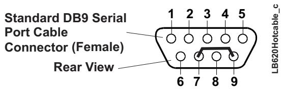
To convert a standard serial cable to a Hot Cable, specific pins must be shorted together at the Serial port connector or on the DB9 cable connector. For example, short the RTS (7) and RI (9) on the respective DB9 port cable connector as shown in Figure 3-2.
![Standard DB9 Serial\nPort Cable\nConnector (Female)\nRear View\n1 2 3 4 5\n6 7 8 9\nLB620Hotcable_c](.50-1z033-1000-lb620-rm-1-0/c764a6e9986241855315b9657d6455126815b27ac36c43046fa5b15438c647cb.jpg)

Figure 3-2. Hot Cable Jumper

# Watchdog Timer

The Watchdog Timer (WDT) restarts the system if a mishap occurs, ensuring proper start-up after the interruption. Possible problems include failure to boot properly, the application software’s loss of control, failure of an interface device, unexpected conditions on the bus, or other hardware or software malfunctions.

The WDT (Watchdog Timer) can be used both during the boot process and during normal system operation.

During the Boot process – If the operating system fails to boot in the time interval set in the BIOS, the system will reset.

Enable the WDT in Boot Settings Configuration of BIOS Setup. Set the WDT for a time-out interval in seconds, between 1 and 255, in one-second increments in the Boot Setting Configuration screen. Ensure you allow enough time for the boot process to complete and for the OS to boot. The OS or application must tickle the WDT as soon as it comes up. This can be done by accessing the hardware directly or through a BIOS call.

During System Operation – An application can set up the WDT hardware through a BIOS call, or by accessing the hardware directly. Some ADLINK Board Support Packages provide an API interface to the WDT. The application must tickle the WDT in the time set when the WDT is initialized or the system will be reset. You can use a BIOS call to tickle the WDT or access the hardware directly.

The BIOS implements interrupt 15 function 0C3h to manipulate the WDT.

# Power Interfaces

# Power In

The LittleBoard 620 uses five separate voltages on the board, but only one of the voltages is provided externally (+5 volts) through the external header, which uses a 7-pin vertical header with 0.156" (3.96mm) pitch. All the onboard voltages are derived from the externally supplied +5 volts DC +/- 5%. The onboard voltages include the CPU core voltages as well as the other voltages used on the board.

Table 3-16 lists the signals for power supply input with 7 pins, single row, and 0.156" (3.96mm) pitch.

Table 3-16. Power In Pin/Signal Descriptions (J19)

<table><tr><td>Pin #</td><td>Signal</td><td>Description</td></tr><tr><td>1</td><td>+5V</td><td>+5.0 Volts – This +5.0 volts DC +/- 5% is the only voltage required for internal operation.</td></tr><tr><td>2</td><td>GND</td><td>Ground</td></tr><tr><td>3</td><td>GND</td><td>Ground</td></tr><tr><td>4</td><td>+12V</td><td>+12 Volts</td></tr><tr><td>5</td><td>+3.3V</td><td>+3.3 Volts</td></tr><tr><td>6</td><td>GND</td><td>Ground</td></tr><tr><td>7</td><td>+5V</td><td>+5.0 Volts – This +5.0 volts DC +/- 5% is the only voltage required for internal operation.</td></tr></table>

Note: The shaded areas denote power or ground. The +12V and +3.3V on the Power In header (J19) are used for the PCI, ISA bus, TTL, and LVDS functions and are supplied externally and not generated on the LittleBoard 620.

# Power On

The signals on this header allow the ATX power supply to be turned off (soft off) from the LittleBoard 620 by operating system (OS) control. However, if you use a non-ATX power supply you will not have the soft off feature normally provided by ATX power supplies.

Table 3-17 lists the signals for the J6 Power On header with 3 pins, single row, and 0.100" (2.54mm) pitch.

Table 3-17. Power On Pin/Signal Descriptions (J6)

<table><tr><td>Pin #</td><td>Signal</td><td>Description</td></tr><tr><td>1</td><td>PS_ON*</td><td>Power Supply On – This signal is sent to the ATX power supply by the LittleBoard 620 to turn On the ATX power supply. This signal can also be used to turn Off the ATX power supply.</td></tr><tr><td>2</td><td>GND</td><td>Ground</td></tr><tr><td>3</td><td>VCCSB</td><td>+5V suspend voltage (+5V, 2A** Standby) – This voltage is supplied from the ATX power supply. This voltage is required for normal operation.</td></tr></table>

Note: The shaded areas denote power or ground. The signals marked with \* = Negative true logic. \*\*The power supply must be capable of delivering 2 amps for 5VSB.

# Power-On Button

A Power-On Button signal is provided by connecting ground to pin 1 on this header (J32). A Reset Switch signal is provided by connecting ground to pin 3 on this header. The J32 header uses a single row of 5 pins with 0.100" (2.54mm) pitch.

Table 3-18. Power-On Button Interface Pin/Signal Descriptions (J32)

<table><tr><td>Pin #</td><td>Signal</td><td>Description</td></tr><tr><td>1</td><td>PWRON</td><td>Power-On Button input (connect between pins 1 &amp; 2)</td></tr><tr><td>2</td><td>GND</td><td>Ground</td></tr><tr><td>3</td><td>RST_SW</td><td>Reset Switch input or output (connect between pins 3 &amp; 2)</td></tr><tr><td>4</td><td>NC</td><td>Not Connected</td></tr><tr><td>5</td><td>NC</td><td>Not Connected</td></tr></table>

Note: The shaded area denotes power or ground.

# Introduction

This section assumes the user is familiar with BIOS Setup and does not attempt to describe the inner workings of BIOS functions. Refer to the appropriate PC reference manuals for information about the onboard, ROM-BIOS software interface. If ADLINK has added to or modified the standard functions, these functions will be described.

# Entering BIOS Setup (VGA Display)

To enter BIOS Setup using a VGA display for the LittleBoard 620:

1. Turn on the VGA monitor and the power supply to the LittleBoard 620.
2. Start Setup by pressing the [Del] key, when the following message appears on the boot screen.

Press DEL to run Setup

# NOTE

If the setting for Memory Test is set to Fast, you may not see this prompt appear on screen if the monitor is too slow to display it on start up. If this happens, press the &lt;Del&gt; key early in the boot sequence to enter BIOS Setup.

3. Use the &lt;Enter&gt; key to select the screen menus listed in the Opening BIOS screen.
4. Follow the instructions at the bottom of each screen to navigate through the selections and modify any settings.

# Entering BIOS Setup (Remote Access)

Once you set up the BIOS Utility for Remote Access (serial console or console redirection) in VGA mode, entering the BIOS in the remote access mode is very similar to the method used when entering the BIOS with a VGA display.

1. Turn on the power supply to the LittleBoard 620 and access the BIOS Setup Utility in VGA mode.
2. Set the BIOS feature Remote Access to [Enabled] under the Advanced menu.
3. Accept the default options or make your own selections for the balance of the Remote Access fields and record your settings.
4. Ensure you select the type of remote serial terminal you will be using and record your selection.
5. Select Save Changes and Exit and then shut down the LittleBoard 620.
6. Connect the remote serial terminal (or the PC with communications software) to the COM port you selected on the LittleBoard 620 using a Hot Cable or a standard null-modem serial cable.
7. Turn on the remote serial terminal (or the PC with communications software) and set it to the settings you selected and recorded earlier in the BIOS Setup Utility.

COM1, 115200, 8 bits, 1 stop bit, no parity, no flow control, and [Always] for Redirection After BIOS POST are the default settings for the LittleBoard 620.

8. Restore power to the LittleBoard 620 and look for the screen prompt shown below.

Press ^C to run SETUP

9. Press the CTRL–C keys to enter Setup early in the boot sequence if Quick Boot is set to [Enabled]. If Quick Boot is set to [Enabled], you may never see the screen prompt.

10. Use the &lt;Enter&gt; key to select the screen menus listed in the Opening BIOS screen.

NOTE The serial console port is not hardware protected, and is not listed in the COM table within BIOS Setup Utility. Diagnostic software that probes hardware addresses may cause a loss or failure of the serial console functions.

# PCI-ISA Bridge Mapping

The LittleBoard 620 supports ISA bus based modules with an on-board PCI-ISA bridge. The PCI-ISA bridge optionally maps the following resources to ISA based modules:

Memory
• I/O Ports
. IRQs

• DMA Channels

The LittleBoard 620 system BIOS maps the above resources, based on information provided in the BIOS Setup screens. By default, only some of the I/O ports are mapped to ISA modules and any memory, IRQs or DMA channels to be mapped must be explicitly specified by the user in the BIOS Setup screens.

The IRQs are mapped with the “PCIPnP/IRQx” fields in BIOS setup (where x specifies the IRQ number.) The IRQs 3, 4, 5, 7, 9, 10, 11, 14, and 15 can be mapped to ISA based modules by changing the default setting for these IRQs from “Available” to “Reserved”.

ISA I/O ports, Memory, and DMA channels can be mapped to ISA modules on the “Boot/Boot Settings Configuration” BIOS setup screen. Six I/O port “windows” and four memory “windows” are available for mapping I/O Port or Memory regions to ISA modules by specifying the window length and base address.

By default, the following I/O port windows are mapped to ISA modules:

• 200-240h
240-260h
. 279h
. 300-340h
• 340-360h
• A79h

NOTE 279h and A79 are the ISA PnP ports used by the BIOS and an OS that supports this feature to recognize ISA PnP (Plug and Play) cards.

By default, no memory windows are mapped to ISA modules.

Any of the DMA channels 0, 1, 2, 3, 5, 6, 7 can be mapped to ISA modules by changing the default setting of “LPC Bridge” to “ISA Bridge”.

For example, to configure an ISA Soundblaster PnP card with resources 220/5/1/5 (Port/IRQ/DMA/DMA) so that the Soundblaster would work in Windows XP, the following BIOS Setup changes would be required:

ISA I/O Ports – no changes necessary. 220h is already mapped to ISA by default.
• IRQ – set IRQ5 to “Reserved” in BIOS Setup. See the paragraph above on mapping IRQs.
DMA1 and DMA5 – set DMA Channels 1 and 5 to “ISA Bridge” in BIOS Setup. See paragraph above on mapping DMA Channels.

# Logo Screen Utility (Splash Screen)

The LittleBoard 620 BIOS supports a graphical logo utility, which can be customized by the user and displayed on screen when enabled through the BIOS Setup Utility. The graphical image can be a company logo or any custom image the user wants to display during the boot process. The custom image can be displayed as the first image displayed on screen during the boot process and remain there, depending on the options selected in BIOS Setup, while the OS boots.

# Logo Screen Image Requirements

The user’s image may be customized with any image editing tool, and the system will automatically convert the image into an acceptable format to the tools (files and utilities) provided by ADLINK.

The LittleBoard 620 OEM logo screen utility supports the following image formats:

Bitmap image
Exactly 640 x 480 pixels
Exactly 16 colors

NOTE For procedures on loading custom images, see the logo screen utility document available on the ADLINK web site.

Bitmap image
16-Color, 640x480 pixels
♦ 256-Color, 640x480 pixels
• JPG image
♦ 16-Color, 640x480 pixels
• PCX image
♦ 256-Color, 640x480 pixels

A file size of not larger than the sample image

NOTE For procedures on loading custom images, see the OEM Logo Utility document available on the ADLINK web site.

ADLINK Technology, Inc. provides a number of methods for contacting Technical Support listed in the Table A-1 below. Requests for support through Ask an Expert are given the highest priority, and usually will be addressed within one working day.

ADLINK Ask an Expert – This is a comprehensive support center designed to meet all your technical needs. This service is free and available 24 hours a day through the Ampro By ADLINK web site at http://www.adlinktech.com/AAE/. This includes a searchable database of Frequently Asked Questions, which will help you with the common information requested by most customers. This is a good source of information to look at first for your technical solutions. However, you must register online if you wish to use the Ask a Question feature.

ADLINK strongly suggests that you register with the web site. By creating a profile on the ADLINK web site, you will have a portal page called “My ADLINK” unique to you with access to exclusive services and account information.

Personal Assistance – You may also request personal assistance by creating an Ask an Expert account and then going to the Ask a Question feature. Requests can be submitted 24 hours a day, 7 days a week. You will receivean immediate confirmation e-mail that your request has been entered. Once you have submitted your request, you must log in to My Stuff where you can check status, update your request, and access other features.
Download Service – This service is also free and available 24 hours a day at http://www.adlinktech.com. For certain downloads such as technical documents and software, you must register online before you can log in to this service.

Table A-1. Technical Support Contact Information

<table><tr><td>Method</td><td>Contact Information</td></tr><tr><td>Ask an Expert</td><td>http://www.adlinktech.com/AAE/</td></tr><tr><td>Web Site</td><td>http://www.adlinktech.com</td></tr><tr><td>Standard Mail</td><td>ADLINK Technology Inc.Address: 9F, No.166 Jian Yi Road, Chungho City,Taipei County 235, Taiwan台北縣中和市建一路166號9樓Tel: +886-2-8226-5877Fax: +886-2-8226-5717Email: service@adlinktech.comAmpro ADLINK Technology Inc.Address: 5215 Hellyer Avenue, #110, San Jose, CA 95138, USATel: +1-408-360-0200Toll Free: +1-800-966-5200 (USA only)Fax: +1-408-360-0222Email: info@adlinktech.comADLINK Technology BeijingAddress: 北京市海淀区上地东路1号盈创动力大厦E座801室(100085)Rm. 801, Power Creative E, No. 1, B/DShang Di East Rd., Beijing 100085, ChinaTel: +86-10-5885-8666Fax: +86-10-5885-8625Email: market@adlinktech.com</td></tr></table>

Table A-1. Technical Support Contact Information

<table><tr><td rowspan="8"></td><td>ADLINK Technology ShanghaiAddress:上海市漕河泾高科技开发区钦江路333号39幢4层(200233)Tel:+86-21-6495-5210Fax:+86-21-5450-0414Email:market@adlinktech.com</td></tr><tr><td>ADLINK Technology ShenzhenAddress:深圳市南山区科技园南区高新南七道数字技术园A1栋2楼C区(518057)2F,C Block,Bld.A1,Cyber-Tech Zone,Gao Xin Ave.Sec 7,High-Tech Industrial Park S.,Shenzhen,518054 ChinaTel:+86-755-2643-4858Fax:+86-755-2664-6353Email:market@adlinktech.com</td></tr><tr><td>ADLINK Technology Inc.(German Liaison Office)Address:Nord Carree 3,40477 Duesseldorf,GermanyTel:+49-211-495-5552Fax:+49-211-495-5557Email:emea@adlinktech.com</td></tr><tr><td>ADLINK (French Liaison Office)Address:15 rue Emile Baudot,91300 MASSY Cedex,FranceTel:+33(0)160123566Fax:+33(0)160123566Email:france@adlinktech.com</td></tr><tr><td>ADLINK Technology Japan CorporationAddress:151-0072東京都渋谷区幡ヶ谷1-1-2朝日生命幡ヶ谷ビル8FAsahiseimei Hatagaya Bldg.8F1-1-2 Hatagaya,Shibuya-ku,Tokyo 151-0072,JapanTel:+81-3-4455-3722Fax:+81-3-5333-6040Email:japan@adlinktech.com</td></tr><tr><td>ADLINK Technology Inc.(Korean Liaison Office)Address:서울시 서초구 서초동1506-25 한도B/D2층2F,Hando B/D,1506-25,Seocho-Dong,Seocho-Gu,Seoul,137-070,KoreaTel:+82-2-2057-0565Fax:+82-2-2057-0563Email:korea@adlinktech.com</td></tr><tr><td>ADLINK Technology Singapore Pte Ltd.Address:84 Genting Lane #07-02A,Cityneon Design Centre,Singapore 349584Tel:+65-6844-2261Fax:+65-6844-2263Email:singapore@adlinktech.com</td></tr><tr><td>ADLINK Technology Singapore Pte Ltd.(Indian Liaison Office)Address:No.1357,&quot;Anupama&quot;,Sri Aurobindo Marg,9th Cross,JP Nagar Phase I,Bangalore - 560078,IndiaTel:+91-80-65605817Fax:+91-80-22443548Email:india@adlinktech.com</td></tr></table>

# A

AT Power in pin-out list . 35

# B

BIOS Setup accessing BIOS setup (VGA) . 37 Logo Screen (Splash) conversion . 39 Watchdog Timer (WDT) . 35

BIOS Setup Utility accessing serial console . 37 using remote access . 37

# C

connectors header list . 10

console redirection serial console . 34 serial port settings . 37 supported feature . 34

Console Redirection See also Remote Access

# D

dimensions . 13

# E

EBX specifications references

Environmental specifications . . 14

Ethernet ports share common ground 12

# H

header pin sequences descriptions 11

Hot cable console redirection . 34 modified serial cable . 34 serial console . 34

# I

Interrupt (IRQs) list . 18

# J

jumper header locations . 13

# L

Lithium Battery RTC . 34

LittleBoard 620 block diagram 7 console redirection feature . 34 dimensions 1 3 EBX Architecture . 3 features . 4 floppy disk drive features . 20 Geode LX800 . 4 GPIO feature . 33 headers 10

Logo Screen (Splash) customization ..39

major integrated circuit list 8

parallel port features .20

pin-1 locations .12

product description 4

see also supported features 4

serial console feature .34

serial port features .21

USB port features .28

Utility 1 interface features .24

voltage requirements . 35, 36

Watchdog Timer (WDT) .35

weight .13

Logo Screen (Splash) customer defined .39 requirements ..39

# M

major chip specifications web sites

major integrated circuits see also major chip specifications

memory map .19

# P

parallel port pin-out list . .20

pin-1 locations .12

power requirements input voltages . 35, 36

processor requirements heatsink requirements .14

# R

Real-Time Clock (RTC) .34 Lithium Battery .34

references EBX specifications PCI-104 specifications specifications

Remote Access serial port settings .37

remote access accessing BIOS .37

Remote Access See also console redirection Remote Access See also serial console

# S

SATA connectors .11

SATA controller .8

SATA interface . .5

Serial A pin-out list . .22

Serial B pin-out list . ..23

Serial Communications Software ..34

serial console

accessing BIOS . 37

console redirection . 34

Hot cable . 34

modified serial cable . 34

serial port settings . 37

serial terminal . 34

serial terminal emulation . 34

terminal emulation software . 34

two methods . 34

Serial Console See also Remote Access

serial terminal

ANSI-compatible . 34

serial terminal emulation . 34

SMBus

supported feature .. 26

specifications

LittleBoard features 4

references

supported features

184-pin DDR DIMM slot . 4

AT power supply input ..35, 36

audio AC’97 interface 6

Battery-free boot 6

console redirection . 34

CRT (VGA) video interface . 29

Ethernet interfaces 6

external battery 6

external battery interface . 25

floppy disk drive ...5, 20

Geode LX800 processor 4

GPIO capability . 33

heatsinks . 14

I/O address map . . 19

IDE devices 5

IRQ assignments . 18

ISA bus . 5

jumper headers, on board 13

LAN Boot . 6

Logo Screen (Splash) customization .... . 39

LVDS interface ..29, 32

memory . 4

memory map . . 19

on-board battery 6

Oops! jumper (BIOS recovery) .... 6, 34

parallel port . 20

PC 'Beep' speaker interface . 25

PC/104 bus . . 5

PC/104-Plus bus 5

power-on switch . 36

PS/2 keyboard interface ... 6, 24

PS/2 mouse interface 6

Real-Time Clock 6

reset switch interface . 25

SATA 5

serial console ... 6, 34

serial ports . ... 5, 21

SMBus devices . 26

thermal monitoring ... 6, 34

USB 2.0 ports 2 8

USB Boot 6

USB boot device 5

USB ports . 5

video interfaces 6

voltage monitoring 6

Watchdog Timer (WDT) ... 6, 35

# T

Technical Support

contact methods . 41

terminal emulation software

serial console 34

thermal cooling

processor requirements 1 4

thermal monitoring

supported feature 34

# V

voltage requirements

AT power supply . 36

#

Watchdog Timer (WDT)

2 to 255 sec interval 35

functions . . 35

web sites

major chip specifications

references

weight 13
[🔗 Link to the original document](.50-1z033-1000-lb620-rm-1-0/50-1z033-1000-lb620-rm-1-0.pdf)