# CoreModule® 740

# Single Board Computer

# Reference Manual

P/N 50-1Z046-1010

# DISCLAIMER

ADLINK Technology, Incorporated makes no representations or warranties with respect to the contents of this manual or of the associated ADLINK products, and specifically disclaims any implied warranties of merchantability or fitness for any particular purpose. ADLINK shall under no circumstances be liable for incidental or consequential damages or related expenses resulting from the use of this product, even if it has been notified of the possibility of such damages. ADLINK reserves the right to revise this publication from time to time without obligation to notify any person of such revisions. If errors are found, please contact ADLINK at the address shown at the bottom of this page.

# TRADEMARKS

CoreModule and the Ampro logo are registered trademarks, and ADLINK, Little Board, LittleBoard, MightyBoard, MightySystem, MilSystem, MiniModule, ReadyBoard, ReadyBox, ReadyPanel, ReadySystem, and RuffSystem are trademarks of ADLINK Technology, Inc. All other marks are the property of their respective companies.

REVISION HISTORY

<table><tr><td>Revision</td><td>Reason for Change</td><td>Date</td></tr><tr><td>1000</td><td>Initial Release</td><td>July/10</td></tr><tr><td>1010</td><td>Revised I/O Paddle Board in App. B; removed JP1 jumper header; removed U13 temp monitor; added BIOS Setup settings to ch. 4; added simplified pin out tables to ch 3</td><td>May/11</td></tr><tr><td></td><td></td><td></td></tr><tr><td></td><td></td><td></td></tr><tr><td></td><td></td><td></td></tr><tr><td></td><td></td><td></td></tr><tr><td></td><td></td><td></td></tr></table>

ADLINK Technology, Incorporated

5215 Hellyer Avenue

San Jose, CA 95138-1007

Tel. 408 360-0200

Fax 408 360-0222

www.adlinktech.com

© Copyright 2010, 2011 ADLINK Technology, Incorporated

# Audience

This manual provides reference only for computer design engineers, including but not limited to hardware and software designers and applications engineers. ADLINK Technology, Inc. assumes you are qualified to design and implement prototype computer equipment.

# Contents

# Chapter 1 About This Manual....1

Purpose of this Manual ....1

References ...... 1

# Chapter 2 Product Overview....3

PC/104 Architecture ....3

Product Description....4

Module Features ....5

Block Diagram 6

Major Components (ICs)....7

Header and Connector Definitions....9

Jumper Header Definition....11

Specifications....11

Physical Specifications ....11

Mechanical Specifications 12

Power Specifications ....13

Environmental Specifications....13

Thermal/Cooling Requirements....13

# Chapter 3 Hardware ....15

Overview....15

Interrupt Channel Assignments ....16

Memory Map ....17

I/O Address Map 17

Utility 1 Interface ....19

Serial Interface....19

Parallel Interface....21

USB Interface 22

Keyboard and Mouse Interfaces....22

Speaker 22

Reset Switch....22

HDD Activity LED....22

Battery Interface 22

Utility 1 Pin Signals....23

Utility 2 Interface ......26

Floppy Drive Interface....26

IDE Interface....27

Utility 2 Pin Signals....28

Video (VGA/LVDS) Interface 32

System Fan....33

Power Interface 33

Miscellaneous ....34

Real Time Clock (RTC) 34

Oops! Jumper (BIOS Recovery)....34

Serial Console 34

Serial Console Setup....34

Hot (Serial) Cable 34

Watchdog Timer ....35

# Chapter 4 BIOS Setup....37

Introduction....37

Entering BIOS Setup (VGA Display) 37

Entering BIOS Setup (Remote Access) 37

PCI-ISA Bridge Mapping 38

OEM Logo Utility 38

Logo Image Requirements....38

BIOS Setup Menus 39

BIOS Main Setup Screen 39

BIOS Advanced Setup Screen 40

BIOS Power Management Setup Screen....42

BIOS Boot Setup Screen 43

BIOS Security Setup Screen 44

BIOS Exit Setup Screen 45

# Appendix A Technical Support 47

# Appendix B I/O Interface Board Description....49

Overview 49

I/O Interface Board Layout 49

I/O Interface Board Connectors and Headers 50

# Index 55

# List of Figures

Figure 2-1. Stacking PC/104-Plus Modules with the CoreModule 740....4

Figure 2-2. Functional Block Diagram 6

Figure 2-3. Component Locations (Top Side)....8

Figure 2-4. Component Locations (Bottom Side) 8

Figure 2-5. Connector Pin Identifications....9

Figure 2-6. Header and Connector Locations (Top Side)....10

Figure 2-7. Header and Connector Locations (Bottom Side)....10

Figure 2-8. Jumper Header Locations (Top Side) 11

Figure 2-9. Mechanical Overview (Top Side) 12

Figure 3-1. Oops! Jumper Serial Port (DB9)....34

Figure 3-2. Serial Console Jumper 34

Figure 4-1. BIOS Main Setup Screen 39

Figure 4-2. BIOS Advanced Setup Screen 40

Figure 4-3. Power Management Setup Screen 42

Figure 4-4. BIOS Boot Setup Screen....43

Figure 4-5. BIOS Security Setup Screen 44

Figure 4-6. BIOS Exit Setup Screen 45

# List of Tables

Table 2-1. Major Component Descriptions and Functions ..... 7

Table 2-2. Module Header and Connector Descriptions ..... 9

Table 2-3. Jumper Settings ...... 11

Table 2-4. Weight and Footprint Dimensions ...... 11

Table 2-5. Power Supply Requirements....13

Table 2-6. Environmental Requirements .... 13

Table 3-1. Interrupt Channel Assignments....16

Table 3-2. Memory Map ...... 17

Table 3-3. I/O Address Map....17

Table 3-4. Simplified Serial Interface (Ports 1 & 2) Pin Signal Descriptions (J5)....19

Table 3-5. Simplified Parallel Interface (SPP) Pin Signal Descriptions (J5)....21

Table 3-6. Simplified USB Interface Pin Signal Descriptions (J5)....22

Table 3-7. Simplified Keyboard, Mouse, and Miscellaneous Pin Signal Descriptions (J5) .....23

Table 3-8. Complete Utility 1 Interface Pin Signals (J5) ......23

Table 3-9. Simplified Floppy Drive Interface Pin Signal Descriptions (J4)....26

Table 3-10. Simplified IDE Interface Pin Signal Descriptions (J4)....27

Table 3-11. Complete Utility 2 Interface Pin Signals (J4) ......28

Table 3-12. Video Interface Pin Signals (J10)....32

Table 3-13. Optional System Fan Pin Signals (J6) ......33

Table 3-14. Power Interface Pin Signals (J7)....33

Table 4-1. BIOS Setup Menus....39

Table A-1. Technical Support Contact Information....47

Table B-1. Utility Interface Pin Signals (J1)....50

Table B-2. Utility Interface Pin Signals (J2)....52

Table B-3. Auxiliary Battery Interface Pin Signals (J10)....53

# Purpose of this Manual

This manual is for designers of systems based on the CoreModule™ 740 single board computer (SBC). This manual contains information that permits designers to create an embedded system based on specific design requirements.

Information provided in this reference manual includes:

• Product Overview
• Hardware Specifications
• BIOS Setup information
• Technical Support Contact Information

Information not provided in this reference manual includes:

• Detailed chip specifications
• Internal component operation
• Internal registers or signal operations
- Bus or signal timing for industry standard busses and signals
• Pinout definitions for industry standard interfaces

# References

The following list of references may help you successfully complete your custom design.

# Specifications

• PC/104 Specification, Revision 2.5, November, 2003
• PC/104-Plus Specification, Revision 2.0, November, 2003
For latest revision of the PC/104 specifications, contact the PC/104 Consortium, at: Web site: http://www.pc104.org
• PCI 2.2 Compliant Specifications, Revision 2.2, December 18, 1998
For latest revision of the PCI specifications, contact the PCI Special Interest Group at: Web site: http://www.pcisig.com
• AMI BIOS Core 8 User's Guide
Data sheet: http://www.ami.com/support/doc/MAN-EZP-80.pdf

# Chip Specifications

The following integrated circuits (ICs) are used in the CoreModule 740 single board computer:

- Intel® Corporation and the N450 processor
Web site:
http://www.intel.com/products/processor/atom/techdocs.htm

• Intel and the ICH8-M chip, used for the I/O Hub (Southbridge)

Data sheet:

http://www.intel.com/assets/pdf/datasheet/313056.pdf

- SMSC and the Super I/O SCH3112I-NU chip used for the Super I/O controller
Data sheet:
http://www.smsc.com/media/Downloads\_Public/Data\_Briefs/311xdb.pdf
- Maxim Integrated Products and the MAX213ECAI+ RS-232 Serial Port transceiver Web site: http://www.maxim-ic.com/quick\_view2.cfm/qv\_pk/1047
- Integrated Technology Express, Inc. and the PCI-to-ISA bridge, IT8888G-L Web site: http://www.iteusa.com or http://www.ite.com.tw

NOTE If you are unable to locate the datasheets using the links provided, go to the manufacturer's web site where you can perform a search using the chip datasheet number or name listed, including the extension (htm for web page, pdf for files name, etc.)

This introduction presents general information about the PC/104 architecture and the CoreModule 740 single board computer (SBC). After reading this chapter you should understand:

• PC/104 architecture
• Product description
• CoreModule 740 features
• Major components (ICs)
- Headers and Connectors
- Specifications

# PC/104 Architecture

The PC/104 architecture affords a great deal of flexibility in system design. You can build a simple system using only a CoreModule 740, an input/output device connected to the serial or parallel ports, and an IDE storage device connected to the IDE port. To expand a simple CoreModule system, simply add self-stacking PC/104 and PC/104-Plus expansion boards to provide additional capabilities, such as:

• Additional serial and parallel ports
• Analog or high-speed digital I/O

♦ Data Acquisition (Analog In/Out)
♦ USB 2.0 expansion modules
♦ IEEE 1394 (FireWire) expansion modules
♦ Standard VGA video output

PC/104 or PC/104-Plus expansion modules can be stacked with the CoreModule 740 avoiding the need for large, expensive card cages and backplanes. The PC/104-Plus expansion modules can be mounted directly to the PC/104 and PC/104-Plus connectors of the CoreModule 740. PC/104-compliant modules can be stacked with an inter-board spacing of $\sim 0.66$ inches, so that a 3-module system fits in a $3.6'' \times 3.8'' \times 2.4''$ space. See Figure 2-1.

One or more MiniModule products or other PC/104 modules can be installed on the CoreModule expansion connectors, so that the expansion modules fit within the CoreModule outline dimensions. Most MiniModule products have stackthrough connectors compatible with the PC/104-Plus Version 2.0 specification. Several modules can be stacked on the CoreModule headers. Each additional module increases the thickness of the package by $\sim 17\mathrm{mm}$ (0.66"). See Figure 2-1.

![Screws (4)\nPC/104 Module\n0.6 inch Spacers (4)\nPCI Stackthrough Connectors\n0.6 inch Spacers (4)\nPC/104-Plus Module\nCoreModule 740\nPCI Stackthrough Connectors\n0.6 inch Spacers (4)\nNuts (4)\nor Chassis Standoffs\nISABus Expansion Stackthrough Connectors\nCM740stackhru](.50-1z046-1010-cm740-referencemanual-final-en/399d00b3f1c75455201ce337f06570bb7b41a181a8d70cc866e8fdacc1c843fd.jpg)

Figure 2-1. Stacking PC/104-Plus Modules with the CoreModule 740

# Product Description

The CoreModule 740 SBC is an exceptionally high integration, high performance, Intel® Atom™ N450 processor based system compatible with the PC/104 standard. This rugged and high quality single-board system contains all the component subsystems of an ATX motherboard plus the equivalent of several PCI expansion boards.

The Intel Atom N400 series CPUs integrate processor cores with Graphics and Memory Hubs (GMHs), providing low-power, high-performance processors, memory controllers for up to 512MB of onboard SDRAM memory, and graphics controllers which provide LVDS and VGA signals for most LCD video panels.

The ICH8-M chipset provides controllers for the I/O Hub (Southbridge) featuring two USB ports, one Ultra DMA 33/66/100 IDE port supporting two IDE devices, and one PCI port. The CoreModule 740 provides legacy interfaces through the SMSC SCH3112I-NU Super I/O featuring two serial ports, one parallel port, PS/2 keyboard and mouse ports, and one floppy port.

The CoreModule 740 can be expanded through the PCI expansion bus using the PC/104 and PC/104-Plus connectors for additional system functions. This bus offers compact, self-stacking, modular expandability. The PC/104 bus is an embedded system version of the signal set provided on a desktop PC's ISA bus. The PC/104-Plus bus includes this signal set plus additional signals implementing a PCI bus, available on a 120-pin (4 rows of 30 pins) PCI expansion bus connector. This PCI bus operates at a clock speed of 33MHz.

The CoreModule 740 is particularly well suited to either embedded or portable applications and meets the size, power consumption, temperature range, quality, and reliability demands of embedded system applications. It can be stacked with ADLINK MiniModules $^{™}$ or other PC/104-compliant expansion modules, or it can be used as a powerful computing engine. The CoreModule 740 requires a single +5V AT power source.

# Module Features

# CPU

♦ Provides 166MHz Intel Atom N450 processor core
♦ DMI (Direct Media Interface) with 1 GB/s of bandwidth in each direction
♦ Enhanced SpeedStep® technology
♦ On die 512-kB, 8-way L2 cache

# - Memory

◆ 512MB standard SDRAM soldered on the board
◆ 667MHz Clock Speed

# - Interface Buses

♦ PC/104 and PC/104-Plus Interfaces
♦ PC/104 bus speeds up to 8MHz (16-bit ISA Bus)
♦ PC/104-Plus bus speed at 33MHz (32-bit PCI Bus)
PCI 2.2 compliant

# • Utility Interfaces (2)

♦ Provide IDE port
• Supports two enhanced IDE devices
• Supports single master mode
• Supports Ultra DMA 100/66/33 in master mode
• Supports ATAPI and DVD peripherals
• Supports IDE native and ATA compatibility modes

♦ Provide floppy drive port
• Supports one floppy drive
• Supports all standard PC/AT formats: 360kB, 1.2MB, 720kB, 1.44MB, 2.88MB
♦ Provide PS/2 Keyboard and PS/2 Mouse ports
♦ Provide parallel printer port with IEEE standard 1284 protocols, and EPP, ECP outputs
♦ Provide two RS-232 serial ports with full handshaking
♦ Provide two 2.0 USB ports
• Provides one root USB hub
- Provides two USB ports
• Supports USB V2.0
♦ Support external reset switch
◆ Support standard external 8Ω speaker interface
♦ Support HDD Activity LED
◆ Support external battery for Real Time Clock operation

• Video Interface (VGA/LVDS)

◆ Supports VGA (1400 x 1050 bpp at 60Hz) with 32MB SMA (Shared Memory Area)
♦ 18-bit flat panel outputs (LVDS)
◆ Supports LVDS (1280 X 800)

\- Miscellaneous

♦ Battery-less boot
- Oops! Jumper support
♦ Serial Console support
♦ Watchdog Timer
♦ Logo Screen (Splash)

# Block Diagram

Figure 2-2 shows the functional components of the module.
![Based on the provided block diagram, here is the accurate and concise description of the labeled blocks and their connections:\n\n**Labeled Blocks:**\n*   Video Header\n*   CPU Intel Atom 1.6GHz N450 (with integrated Northbridge)\n*   DDR2 SDRAM Soldered (4)\n*   I/O Hub Intel ICH8-M (Southbridge)\n*   PC/104-Plus Connector\n*   PCI to ISA Bridge IT8888G-L\n*   PC/104 Connector\n*   RS-232 Transceiver (COM1)\n*   Super I/O SCH3112I-NU\n*   RS-232 Transceiver (COM2)\n*   80-pin Utility Connector 1 (containing sub-blocks: 2 Serial Ports, 2 USB Ports, Keyboard/Mouse, Speaker, Parallel, Reset Switch, HDD LED, Battery)\n*   80-pin Utility Connector 2 (containing sub-blocks: Floppy, IDE)\n\n**Connections:**\n*   **Video Header** connects to the **CPU** via lines labeled **LVDS** and **VGA**.\n*   The **CPU** connects to **DDR2 SDRAM Soldered (4)** via a line labeled **Memory Bus**.\n*   The **CPU** connects to the **I/O Hub Intel ICH8-M (Southbridge)** via a line labeled **DMI**.\n*   The **I/O Hub** connects to the **PCI to ISA Bridge IT8888G-L** via a line labeled **PCI Bus**.\n*   The **PCI to ISA Bridge** connects to the **PC/104-Plus Connector**.\n*   The **PCI to ISA Bridge** connects to the **PC/104 Connector** via a line labeled **ISA Bus**.\n*   The **I/O Hub** connects to the **Super I/O SCH3112I-NU** via a line labeled **LPC Bus**.\n*   The **I/O Hub** connects to the **IDE** line (leading to **80-pin Utility Connector 2** -) **IDE**) and the **USB (2)** line (leading to **80-pin Utility Connector 1** -) **2 USB Ports**).\n*   The **Super I/O** connects to **RS-232 Transceiver (COM1)** and **RS-232 Transceiver (COM2)**.\n*   **RS-232 Transceiver (COM1)** and **RS-232 Transceiver (COM2)** connect to **80-pin Utility Connector 1** -) **2 Serial Ports**.\n*   The **Super I/O** connects via lines labeled **PS/2** and **LPT** to **80-pin Utility Connector 1** -) **Keyboard/Mouse** and **Parallel**, respectively.\n*   The **Super I/O** connects via a line labeled **Floppy** to **80-pin Utility Connector 2** -) **Floppy**.](.50-1z046-1010-cm740-referencemanual-final-en/713f5e346e798e4c2a2cf03c08961b365b70ae88257232966d59fb3e62a55753.jpg)

Figure 2-2. Functional Block Diagram

# Major Components (ICs)

Table 2-1 lists the major ICs, including a brief description of each, on the CoreModule 740. Figures 2-3 and 2-4 show the locations of the major ICs.
Table 2-1. Major Component Descriptions and Functions

<table><tr><td>Chip Type</td><td>Mfg.</td><td>Model</td><td>Description</td><td>Function</td></tr><tr><td>CPU (U1)</td><td>Intel</td><td>Atom N450</td><td>Central Processing Unit</td><td>Integrated processor core and Northbridge (memory and video)</td></tr><tr><td>I/O Hub (U2)</td><td>Intel</td><td>82801HBM ICH8-M</td><td>Southbridge functions (provides some of standard I/O functions)</td><td>I/O functions</td></tr><tr><td>PCI-to-ISA Bridge (U8 - on bottom side) [see Figure 2-4]</td><td>ITE</td><td>ITE8888G-L</td><td>PCI-to-ISA interface</td><td>ISA bus support</td></tr><tr><td>Super I/O Hub (U9 - on bottom side) [see Figure 2-4]</td><td>SMSC</td><td>SCH3112I-NU</td><td>Super I/O controller provides remaining standard I/O functions</td><td>I/O functions</td></tr><tr><td>RS-232 Transceiver (U11 - on bottom side) [see Figure 2-4]</td><td>Maxim*</td><td>MAX213ECAI+*</td><td>RS232 Transceiver for COM1</td><td>Serial Port Transceiver</td></tr><tr><td>RS-232 Transceiver (U12 - on bottom side) [see Figure 2-4]</td><td>Maxim*</td><td>MAX213ECAI+*</td><td>RS232 Transceiver for COM2</td><td>Serial Port Transceiver</td></tr><tr><td>Soldered Memory (U27)</td><td>Elpida*</td><td>EDE1116AEBG-8E-F*</td><td>SDRAM 1</td><td>128MB DDR2 memory</td></tr><tr><td>Soldered Memory (U28 - on bottom side) [see Figure 2-4]</td><td>Elpida*</td><td>EDE1116AEBG-8E-F*</td><td>SDRAM 2</td><td>128MB DDR2 memory</td></tr><tr><td>Soldered Memory (U29)</td><td>Elpida*</td><td>EDE1116AEBG-8E-F*</td><td>SDRAM 3</td><td>128MB DDR2 memory</td></tr><tr><td>Soldered Memory (U30) - on bottom side [see Figure 2-4]</td><td>Elpida*</td><td>EDE1116AEBG-8E-F*</td><td>SDRAM 4</td><td>128MB DDR2 memory</td></tr></table>

Note: \*Subject to change in model or manufacturer.

Key:

U1 - CPU

U2 - Southbridge

U27 - SDRAM 1

U29 - SDRAM 3

![U27\nSAMSUNG EASTI\nU1\nU29\nSAMSUNG EASTI\nU2\nCM740_Top_Comp_b](.50-1z046-1010-cm740-referencemanual-final-en/c196b1aee57750848108d0c312b626830af76389e936a34f53be32b3095176ac.jpg)

Figure 2-3. Component Locations (Top Side)

Key:

U8 - ISA Bridge

U9 - SIO

U11 - RS-232 Transceiver1

U12 - RS-232 Transceiver2

U28 - SDRAM 2

U30 - SDRAM 4

![ver1\nver2\nU11\nU12\nU28\nU30\nU9\nU8](.50-1z046-1010-cm740-referencemanual-final-en/d06b384fee2ec0f84da0d97468b7d7cd55aad5a6a3de20842e63ec4fe190681c.jpg)

Figure 2-4. Component Locations (Bottom Side)
CM740\_Bottom\_Comp\_b

# Header and Connector Definitions

Table 2-2 describes the headers and connectors of the CoreModule 740 shown in Figures 2-6 and 2-7.

Table 2-2. Module Header and Connector Descriptions

<table><tr><td>Header #</td><td>Board Access</td><td>Description</td></tr><tr><td>J1 A, B, C, D – PC/104-Plus</td><td>Top/Bottom</td><td>120-pin, 0.079&quot; (2mm) connector used for PC/104-Plus signals</td></tr><tr><td>J2 A, B, C, D – PC/104</td><td>Top/Bottom</td><td>104-pin, connector used for PC/104 signals</td></tr><tr><td>J4 – Utility 2</td><td>Top</td><td>80-pin, 0.025&quot; (0.635mm) High-Density connector used for Floppy and IDE signals</td></tr><tr><td>J5 – Utility 1</td><td>Top</td><td>80-pin, 0.025&quot; (0.635mm) High-Density connector used for Serial, Parallel, USB 1 &amp; 2, Keyboard and Mouse, Speaker, Reset Switch, HDD Activity LED, and Battery</td></tr><tr><td>J6 – Fan</td><td>Top</td><td>2-pin, 0.079&quot; (2mm) header used for System Fan signals</td></tr><tr><td>J7 – Power</td><td>Top</td><td>10-pin, 0.100&quot; (2.54mm), right-angle, shrouded header used for external power connection</td></tr><tr><td>J8 – N/P</td><td>Bottom</td><td>Not Populated</td></tr><tr><td>J9 – N/P</td><td>Bottom</td><td>Not Populated</td></tr><tr><td>J10 – Video</td><td>Bottom; see Figure 2-7</td><td>30-pin, 0.079&quot; (2mm) header used for LVDS and VGA video signals</td></tr><tr><td>J11 – N/P</td><td>Bottom</td><td>Not Populated</td></tr><tr><td>J12 – N/S</td><td>Bottom; see Figure 2-7</td><td>Not Supported</td></tr></table>

# NOTE

The pinout tables in Chapter 3 of this manual identify pin sequence using the following methods: A 30-pin header with two rows of pins, using odd/even numbering, where pin 2 is directly across from pin 1, is noted as 30-pin, 2 rows, odd/even (1, 2). Alternately, a 30-pin connector using consecutive numbering, where pin 11 is directly across from pin 1, is noted in this way: 30-pin, 2 rows, consecutive (1, 11). The second number in the parenthesis is always directly across from pin 1. See Figure 2-5.

![| Row Type | Odd/Even | 1 | 2 | 3 |\n|----------|----------|---|---|---|\n| 30-pin   | Odd/Even | 29 | 19 | 9 |\n| 30-pin   | Odd/Even | 19 | 9 | 7 |\n| 30-pin   | Odd/Even | 9 | 5 | 3 |\n| 30-pin   | Odd/Even | 3 | 1 | 1 |\n| Or       | Odd/Even | 30 | 20 | 10 |\n| Or       | Odd/Even | 20 | 10 | 8 |\n| Or       | Odd/Even | 10 | 6 | 4 |\n| Or       | Odd/Even | 2 | 2 | 2 |\n| Or       | Consecutive | 30 | 20 | 15 |\n| Or       | Consecutive | 20 | 15 | 11 |\n| Or       | Consecutive | 15 | 10 | 5 |\n| Or       | Consecutive | 2 | 1 | 2 |\n| Or       | Consecutive | 11 | 11 | 11 |\nCM740_ConNum.a](.50-1z046-1010-cm740-referencemanual-final-en/df98b32f74d1c4bc290f1c1a57e1f8447c508230b8f19bd6a8ef93a4ead716ee.jpg)

Figure 2-5. Connector Pin Identifications
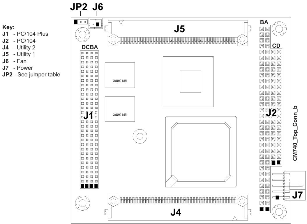
![JP2 J6\nKey:\nJ1 - PC/104 Plus\nJ2 - PC/104\nJ4 - Utility 2\nJ5 - Utility 1\nJ6 - Fan\nJ7 - Power\nJP2 - See jumper table\nDCBA\nJ5\nSAMSUNG K83I\nSAMSUNG K83I\nJ1\nJ4\nBA\nCD\nCM740_Top_Conn_b\nJ2\nJ7](.50-1z046-1010-cm740-referencemanual-final-en/a7bb432af483006ca8de0a7404fa48bc189880da95147b0d195c30a8c8793736.jpg)

Figure 2-6. Header and Connector Locations (Top Side)
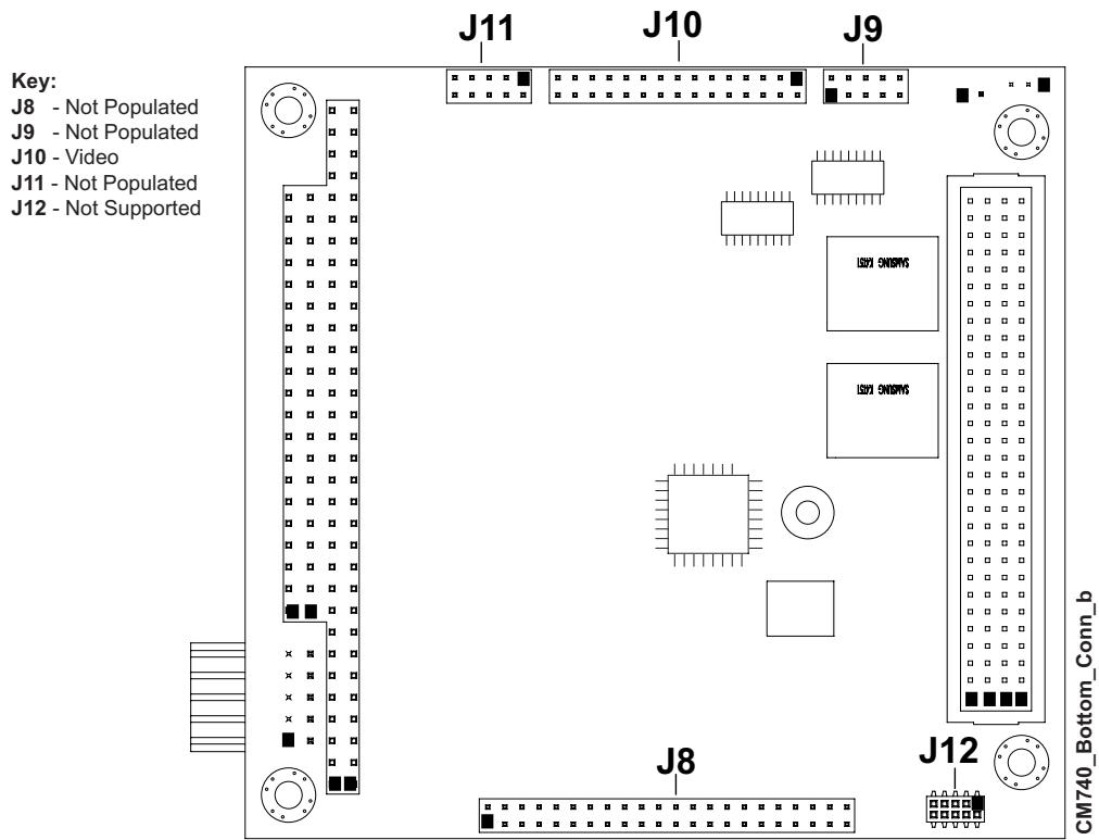
![Key:\nJ8 - Not Populated\nJ9 - Not Populated\nJ10 - Video\nJ11 - Not Populated\nJ12 - Not Supported\nJ11\nJ10\nJ9\nJ8\nJ12\nCM740_Bottom_Conn_b](.50-1z046-1010-cm740-referencemanual-final-en/22d20104533455fb076c5f8e04934fa5028228e9d36198a5687c3d50964ff368.jpg)

Figure 2-7. Header and Connector Locations (Bottom Side)

# Jumper Header Definition

Table 2-3 describes the jumper header shown in Figure 2-8. All jumper headers provide 0.079" (2mm) pitch.

Table 2-3. Jumper Settings

<table><tr><td>Jumper Header</td><td>Installed</td><td>Removed/Enabled</td></tr><tr><td>JP2 – LVDS Voltage Selection</td><td>Enable +3.3V (1-2) (Default)</td><td>Enable +5V (2-3)</td></tr></table>

Key:

JP2 - LVDS Voltage Selection

JP2
![CM740_Top_Jmpr_b\nSAMSUNG EAST\nSAMSUNG EAST](.50-1z046-1010-cm740-referencemanual-final-en/63318309ba5ac78586cae3a25ac898ad7e0b2737efde68f9ef0dbe6fac59d15f.jpg)

Figure 2-8. Jumper Header Locations (Top Side)

# Specifications

# Physical Specifications

Table 2-4 gives the physical dimensions of the module.

Table 2-4. Weight and Footprint Dimensions

<table><tr><td>Item</td><td>Dimension</td><td rowspan="6">NOTE</td><td rowspan="6">Overall height is measured from the upper board surface to the highest permanent component (PC/104 bus connector) on the upper board surface. This measurement does not include the heatsink, which can vary. The heatsink could increase this dimension.</td></tr><tr><td>Weight</td><td>0.12 kg (0.25 lbs)</td></tr><tr><td>Height (overall)</td><td>11.05 mm (0.435 inches)</td></tr><tr><td>Board thickness</td><td>2.362 mm (0.093 inches)</td></tr><tr><td>Width</td><td>90.169 mm (3.55 inches)</td></tr><tr><td>Length</td><td>95.884 mm (3.775 inches)</td></tr></table>

# Mechanical Specifications

![3.250\n3.550\n3.350\nSAMSUNG KENT\nSAMSUNG KENT\nCM740_Dmn_b\n0.350\n0.200\n0.000\n0.000\n0.200\n3.775\n3.575\n0.000\n3.250\n3.350\n3.550\n3.350\n0.350\n0.000\n3.775](.50-1z046-1010-cm740-referencemanual-final-en/6db062dd78a51b557f6812c04e91a4a5fd03bebedba0bab9f8176b627b6e4ce3.jpg)

Figure 2-9. Mechanical Overview (Top Side)

NOTE All dimensions are given in inches. Pin 1 is shown as a black square on headers and connectors. Black squares on right-angle headers indicate pin 2 in top-side views and pin 1 in bottom-side views.

# Power Specifications

Table 2-5 provides the power requirements for the CoreModule 740.
Table 2-5. Power Supply Requirements

<table><tr><td>Parameter</td><td>1.6GHz Characteristics</td></tr><tr><td>Input Type</td><td>Regulated DC voltage</td></tr><tr><td>In-rush Voltage &amp; Current (Max)</td><td>7.16A (35.80W)</td></tr><tr><td>Typical Idle Voltage &amp; Current</td><td>1.28A (6.42W)</td></tr><tr><td>BIT Voltage &amp; Current</td><td>1.78A (8.92W)</td></tr></table>

# Operating configurations:

- In-rush operating configuration includes Intel Atom N450 CPU, video, 512MB built-in SDRAM, and power.
- Idle operating configuration includes In-rush configuration as well as connected I/O board, one external PATA HDD (primary master), one external IDE CD-ROM (Primary Slave), one external floppy drive, one PS/2 keyboard, and one PS/2 mouse.
- BIT (Burn-In-Test) operating configuration includes Idle configuration as well as one USB Compact Flash reader with 64MB Compact Flash, one USB flash thumb drive, one LPT loop back, and two serial loop backs.

# Environmental Specifications

Table 2-6 provides the most efficient operating and storage condition ranges required for this module.
Table 2-6. Environmental Requirements

<table><tr><td>Parameter</td><td>Conditions</td></tr><tr><td>Temperature</td><td></td></tr><tr><td>Operating</td><td>-20 to +70 C (-4 to +158 F)</td></tr><tr><td>Extended (Optional)</td><td>-40 to +85 C (-40 to +185 F)</td></tr><tr><td>Storage</td><td>-55 to +85 C (-67 to +185 F)</td></tr><tr><td>Humidity</td><td></td></tr><tr><td>Operating</td><td>5% to 90% relative humidity, non-condensing</td></tr><tr><td>Non-operating</td><td>5% to 95% relative humidity, non-condensing</td></tr></table>

# Thermal/Cooling Requirements

The CPU is the primary source of heat on the board. The CoreModule 740 is designed to operate at the maximum speed of the CPU and requires a heatsink (provided).

# Overview

This chapter discusses the chips and connectors of the module features in the following order:

- Memory Map
- Interrupt Channel Assignments
- I/O Address Map
• Utility 1 Interface

♦ Serial 1 & 2 Interfaces
♦ Parallel Interface
USB 1 & 2 Interfaces
Mouse
♦ Keyboard
♦ Speaker
Reset Switch
♦ HDD Activity LED
♦ Battery

• Utility 2 Interface
♦ Floppy Interface
IDE Signals

- Video Interface
♦ VGA
LVDS

\- System Fan

\- Power Interface

\- Miscellaneous

Time of Day/RTC
- Oops! Jumper
Serial Console
♦ Watchdog Timer

# NOTE

ADLINK Technology, Inc. supports only the features/options tested and listed in this manual. The main chips used in the CoreModule 740 may provide more features or options than are listed for the CoreModule 740, but some of these features/options are not supported on the module and will not function as specified in the chip documentation.

The pinout tables only of non-standard headers and connectors are included in this chapter. This chapter does not include pinout tables for standard headers and connectors such as PC/104 and PC/104-Plus.

# Interrupt Channel Assignments

The interrupt channel assignments are shown in Table 3-1.

Table 3-1. Interrupt Channel Assignments

<table><tr><td>Device vs IRQ No.</td><td>0</td><td>1</td><td>2</td><td>3</td><td>4</td><td>5</td><td>6</td><td>7</td><td>8</td><td>9</td><td>10</td><td>11</td><td>12</td><td>13</td><td>14</td><td>15</td></tr><tr><td>Timer</td><td>X</td><td></td><td></td><td></td><td></td><td></td><td></td><td></td><td></td><td></td><td></td><td></td><td></td><td></td><td></td><td></td></tr><tr><td>Keyboard</td><td></td><td>X</td><td></td><td></td><td></td><td></td><td></td><td></td><td></td><td></td><td></td><td></td><td></td><td></td><td></td><td></td></tr><tr><td>Secondary Cascade</td><td></td><td></td><td>X</td><td></td><td></td><td></td><td></td><td></td><td></td><td></td><td></td><td></td><td></td><td></td><td></td><td></td></tr><tr><td>COM1</td><td></td><td></td><td></td><td>O</td><td>D</td><td></td><td></td><td></td><td></td><td></td><td></td><td></td><td></td><td></td><td></td><td></td></tr><tr><td>COM2</td><td></td><td></td><td></td><td>D</td><td>O</td><td></td><td></td><td></td><td></td><td></td><td></td><td></td><td></td><td></td><td></td><td></td></tr><tr><td>Floppy</td><td></td><td></td><td></td><td></td><td></td><td></td><td>D</td><td></td><td></td><td></td><td></td><td></td><td></td><td></td><td></td><td></td></tr><tr><td>Parallel</td><td></td><td></td><td></td><td></td><td></td><td>O</td><td></td><td>D</td><td></td><td></td><td></td><td></td><td></td><td></td><td></td><td></td></tr><tr><td>RTC</td><td></td><td></td><td></td><td></td><td></td><td></td><td></td><td></td><td>X</td><td></td><td></td><td></td><td></td><td></td><td></td><td></td></tr><tr><td>IDE</td><td></td><td></td><td></td><td></td><td></td><td></td><td></td><td></td><td></td><td></td><td></td><td></td><td></td><td></td><td>D</td><td></td></tr><tr><td>Math Coprocessor</td><td></td><td></td><td></td><td></td><td></td><td></td><td></td><td></td><td></td><td></td><td></td><td></td><td></td><td>X</td><td></td><td></td></tr><tr><td>PS/2 Mouse</td><td></td><td></td><td></td><td></td><td></td><td></td><td></td><td></td><td></td><td></td><td></td><td></td><td>X</td><td></td><td></td><td></td></tr><tr><td>PCI INTA</td><td colspan="16">Automatically Assigned</td></tr><tr><td>PCI INTB</td><td colspan="16">Automatically Assigned</td></tr><tr><td>PCI INTC</td><td colspan="16">Automatically Assigned</td></tr><tr><td>PCI INTD</td><td colspan="16">Automatically Assigned</td></tr><tr><td>USB</td><td colspan="16">Automatically Assigned</td></tr><tr><td>Video</td><td colspan="16">Automatically Assigned</td></tr></table>

Legend: D = Default, O = Optional, X = Fixed

NOTE The IRQs for USB and Video are automatically assigned by the BIOS Plug and Play logic. Local IRQs assigned during initialization can not be used by external devices.

# Memory Map

The following table provides the common PC/AT memory allocations. These are DOS-level addresses. The OS typically hides these physical addresses by way of memory management. Memory below 000500h is used by the BIOS.

Table 3-2. Memory Map

<table><tr><td colspan="2">Base Address</td><td>Function</td></tr><tr><td>00000000h</td><td>- 0009FFFFh</td><td>Conventional Memory</td></tr><tr><td>000A0000h</td><td>- 000AFFFFh</td><td>Graphics Memory</td></tr><tr><td>000B0000h</td><td>- 000B7FFFh</td><td>Mono Text Memory</td></tr><tr><td>000B8000h</td><td>- 000BFFFFh</td><td>Color Text Memory</td></tr><tr><td>000C0000h</td><td>- 000CFFFFh</td><td>Standard Video BIOS</td></tr><tr><td>000D0000h</td><td>- 000DFFFFh</td><td>Reserved for Extended BIOS</td></tr><tr><td>000E0000h</td><td>- 000EFFFFh</td><td>Extended System BIOS Area</td></tr><tr><td>000F0000h</td><td>- 000FFFFFFh</td><td>System BIOS Area (Storage and RAM Shadowing)</td></tr><tr><td>00100000h</td><td>- 04000000h</td><td>Extended Memory (If onboard VGA is enabled, then the amount of memory assigned is subtracted from extended memory.)</td></tr><tr><td>FFF80000h</td><td>- FFFFFFFH</td><td>System Flash</td></tr></table>

# I/O Address Map

Table 3-3 shows the I/O address map. These are DOS-level addresses. The OS typically hides these physical addresses by way of memory management.

Table 3-3. I/O Address Map

<table><tr><td>Address (hex)</td><td>Subsystem</td></tr><tr><td>0000-000F</td><td>Primary DMA Controller</td></tr><tr><td>0020-0021</td><td>Master Interrupt Controller</td></tr><tr><td>0040-0043</td><td>Programmable Interrupt Timer (Clock/Timer)</td></tr><tr><td>0060</td><td>Keyboard Controller</td></tr><tr><td>0061</td><td>NMI, Speaker Control</td></tr><tr><td>0063</td><td>NMI Controller</td></tr><tr><td>0064</td><td>Keyboard Controller</td></tr><tr><td>0065</td><td>NMI Controller</td></tr><tr><td>0067</td><td>NMI Controller</td></tr><tr><td>0070-007F</td><td>CMOS RAM, NMI Mask Reg, RT Clock</td></tr><tr><td>0080</td><td>System reserved</td></tr><tr><td>0081-0083</td><td>DMA Page Registers</td></tr><tr><td>0084-0086</td><td>System reserved</td></tr><tr><td>0087</td><td>DMA Page Register</td></tr><tr><td>0088</td><td>System reserved</td></tr><tr><td>0089-008B</td><td>DMA Page Registers</td></tr><tr><td>008C-008E</td><td>System reserved</td></tr><tr><td>008F</td><td>DMA Page Register</td></tr><tr><td>0090-0091</td><td>System reserved</td></tr><tr><td>0092</td><td>Fast A20 gate and CPU reset</td></tr><tr><td>0093-009F</td><td>System reserved</td></tr><tr><td>00A0-00A1</td><td>Slave Interrupt Controller</td></tr><tr><td>00A2-00BF</td><td>System reserved</td></tr><tr><td>00C0-00DF</td><td>Slave DMA Controller #2</td></tr><tr><td>00E0-00EF</td><td>System reserved</td></tr><tr><td>00F0-00FF</td><td>Math Coprocessor</td></tr><tr><td>01F0-01F7</td><td>IDE Hard Disk Controller</td></tr><tr><td>0200-0240h</td><td>Mapped to ISA</td></tr><tr><td>0240-0260h</td><td>Mapped to ISA</td></tr><tr><td>0279h</td><td>Mapped to ISA</td></tr><tr><td>02F8-02FF</td><td>Serial Port 2 (COM2)</td></tr><tr><td>0300-0340h</td><td>Mapped to ISA</td></tr><tr><td>0340-0360h</td><td>Mapped to ISA</td></tr><tr><td>0378-037F</td><td>Parallel Port (Standard and EPP)</td></tr><tr><td>03B0-03BB</td><td>Video (monochrome)</td></tr><tr><td>03C0-03DF</td><td>Video (VGA)</td></tr><tr><td>03F0-03F5</td><td>Floppy Disk Controller</td></tr><tr><td>03F6</td><td>IDE Hard Disk Controller</td></tr><tr><td>03F7</td><td>Floppy Disk Controller</td></tr><tr><td>03F8-03FF</td><td>Serial Port 1 (COM1)</td></tr><tr><td>04D0-04D1</td><td>Edge/Level Trigger PIC</td></tr><tr><td>0778-077F</td><td>Parallel Port (ECP Extensions) (Port 378+400)</td></tr><tr><td>0A79h</td><td>Mapped to ISA</td></tr><tr><td>0CF8-0CFF</td><td>PCI Configuration Registers</td></tr><tr><td>0CF9</td><td>Reset Control Register</td></tr></table>

NOTE 0279h and 0A79h are the ISA PnP ports used by the BIOS and an OS that supports this feature to recognize ISA PnP (Plug and Play) cards.
The Intel I/O hub ICH-8 (ICH-6 or later) does not support ISA DMA.

# Utility 1 Interface

The CoreModule 740 provides two utility interface connectors. Both interfaces, Utility 1 (J5) and Utility 2 (J4), use identical 80-pin connectors. This section describes the Utility 1, J5 interface, which supports the features listed in the following bullets. Table 3-8 provides a complete list of the Utility 1 connector interface signals. Tables 3-4 through 3-7 provide simplified pin signal descriptions of each specific interface on the Utility 1 connector.

- Serial interface
- Parallel interface
- USB interface
• Mouse and Keyboard interfaces
- Speaker interface
- Reset Switch interface
• HDD Activity LED interface
- Battery interface

# Serial Interface

The two serial port signals are provided through the 80-pin Utility 1 connector (J5) and support the following features:

• Both ports are 16550 compatible
• Programmable word length, stop bits and parity
• 16-bit programmable baud rate and Interrupt generator
- Loop-back mode
- Two 16-bit FIFOs and two DMA handshake lines
• Serial 1 and 2 (COM 1 and COM 2) support RS-232

Note: The shaded table cells denote power or ground. The \* symbol indicates the signal is Active Low.
Table 3-4. Simplified Serial Interface (Ports 1 & 2) Pin Signal Descriptions (J5)

<table><tr><td>J5 Pin #</td><td>Signal</td><td>DB25 Pin #</td><td>DB9 Pin #</td><td>Description</td></tr><tr><td>1</td><td>DCD1*</td><td>8</td><td>1</td><td>Data Carrier Detect 1 – Indicates external modem is detecting a carrier signal (i.e., a communication channel is currently open). In direct connect environments, this input will be driven by DTR1 as part of the DTR1/DSR1 handshake.</td></tr><tr><td>3</td><td>DSR1*</td><td>6</td><td>6</td><td>Data Set Ready 1 – Indicates external serial communications device is powered, initialized, and ready. Used as hardware handshake with DTR1 for overall readiness to communicate.</td></tr><tr><td>5</td><td>RXD1</td><td>3</td><td>2</td><td>Serial Port Receive Data 1 Input – This line is typically held at a logic 1 (mark) when no data is being transmitted, and is held “Off” for a brief interval after an “On” to “Off” transition on the RTS1 line to allow the transmission to complete.</td></tr><tr><td>7</td><td>RTS1*</td><td>4</td><td>7</td><td>Request To Send 1 – Indicates serial port is ready to transmit data. Used as hardware handshake with CTS1 for low level flow control.</td></tr><tr><td>9</td><td>TXD1</td><td>2</td><td>3</td><td>Serial Port Transmit Data 1 Output – This line is typically held to a logic 1 when no data is being sent. Typically, a logic 0 (On) must be present on RTS1, CTS1, DSR1, and DTR1 before data can be transmitted on this line.</td></tr><tr><td>11</td><td>CTS1*</td><td>5</td><td>8</td><td>Clear To Send 1 – Indicates external serial communication device is ready to receive data. Used as hardware handshake with RTS1 for low level flow control.</td></tr><tr><td>13</td><td>DTR1*</td><td>20</td><td>4</td><td>Data Terminal Ready 1 – Indicates port is powered, initialized, and ready. Used as hardware handshake with DSR1 for overall readiness to communicate.</td></tr><tr><td>15</td><td>RI1*</td><td>22</td><td>9</td><td>Ring Indicator 1 – Indicates external modem is detecting a ring condition. Used by software to initiate operations to answer and open the communications channel.</td></tr><tr><td>17</td><td>GND</td><td>7</td><td>5</td><td>Digital Ground</td></tr><tr><td>19</td><td>NC</td><td>NC</td><td>NC</td><td>Not Connected</td></tr><tr><td>21</td><td>DCD2*</td><td>8</td><td>1</td><td>Data Carrier Detect 2 – Indicates external modem is detecting a carrier signal (i.e., a communication channel is currently open). In direct connect environments, this input will be driven by DTR2 as part of the DTR2/DSR2 handshake.</td></tr><tr><td>23</td><td>DSR2*</td><td>6</td><td>6</td><td>Data Set Ready 2 – Indicates external serial communications device is powered, initialized, and ready. Used as hardware handshake with DTR2 for overall readiness to communicate.</td></tr><tr><td>25</td><td>RXD2</td><td>3</td><td>2</td><td>Serial Port Receive Data 2 Input – This line is typically held at a logic 1 (mark) when no data is being transmitted, and is held “Off” for a brief interval after an “On” to “Off” transition on the RTS2 line to allow the transmission to complete.</td></tr><tr><td>27</td><td>RTS2*</td><td>4</td><td>7</td><td>Request To Send 2 – Indicates serial port is ready to transmit data. Used as hardware handshake with CTS2 for low level flow control.</td></tr><tr><td>29</td><td>TXD2</td><td>2</td><td>3</td><td>Serial Port Transmit Data 2 Output – This line is typically held to a logic 1 when no data is being sent. Typically, a logic 0 (On) must be present on RTS2, CTS2, DSR2, and DTR2 before transmitting data on this line.</td></tr><tr><td>31</td><td>CTS2*</td><td>5</td><td>8</td><td>Clear To Send 2 – Indicates external serial communication device is ready to receive data. Used as hardware handshake with RTS2 for low level flow control.</td></tr><tr><td>33</td><td>DTR2*</td><td>20</td><td>4</td><td>Data Terminal Ready 2 – Indicates port is powered, initialized, and ready. Used as hardware handshake with DSR2 for overall readiness to communicate.</td></tr><tr><td>35</td><td>RI2*</td><td>22</td><td>9</td><td>Ring Indicator 2 – Indicates external modem is detecting a ring condition. Used by software to initiate operations to answer and open the communications channel.</td></tr><tr><td>37</td><td>GND</td><td>7</td><td>5</td><td>Digital Ground</td></tr><tr><td>39</td><td>TXD2_ TTL</td><td>NC</td><td>NC</td><td>Serial Transmit Data 2 – Serial port 2 TTL transmit data output signal (jumped to pin 3 DB9 connector on I/O Board).</td></tr></table>

# Parallel Interface

The parallel port interface supports standard parallel, Bi-directional, ECP and EPP protocols. The Super I/O chip (SCH3112I-NU) provides the parallel port interface signals to support Standard Printer Port (SPP), Enhanced Parallel Port (EPP), and Enhanced Capabilities Port (ECP) protocols.

Table 3-5. Simplified Parallel Interface (SPP) Pin Signal Descriptions (J5)

<table><tr><td>J5 Pin #</td><td>Signal</td><td>DB25 Pin #</td><td>Description</td></tr><tr><td>2</td><td>Strobe*</td><td>1</td><td>Strobe* – This output signal is used to strobe data into the printer. I/O pin in ECP/EPP mode.</td></tr><tr><td>6</td><td>PD0</td><td>2</td><td>Parallel Port Data 0 – This pin (0 to 7) provides a parallel port data signal and is the LSB of printer data.</td></tr><tr><td>10</td><td>PD1</td><td>3</td><td>Parallel Port Data 1 – Refer to pin 6 (J5) for more information.</td></tr><tr><td>14</td><td>PD2</td><td>4</td><td>Parallel Port Data 2 – Refer to pin 6 (J5) for more information.</td></tr><tr><td>18</td><td>PD3</td><td>5</td><td>Parallel Port Data 3 – Refer to pin 6 (J5) for more information.</td></tr><tr><td>22</td><td>PD4</td><td>6</td><td>Parallel Port Data 4 – Refer to pin 6 (J5) for more information.</td></tr><tr><td>26</td><td>PD5</td><td>7</td><td>Parallel Port Data 5 – Refer to pin 6 (J5) for more information.</td></tr><tr><td>30</td><td>PD6</td><td>8</td><td>Parallel Port Data 6 – Refer to pin 6 (J5) for more information.</td></tr><tr><td>34</td><td>PD7</td><td>9</td><td>Parallel Port Data 7 – This pin (0 to 7) provides a parallel port data signal and is the MSB of printer data.</td></tr><tr><td>38</td><td>ACK*</td><td>10</td><td>Acknowledge * – This is a status input signal from the printer. A Low State indicates it has received the data and is ready to accept new data.</td></tr><tr><td>42</td><td>BUSY</td><td>11</td><td>Busy – This is a status input signal from the printer. A high state indicates the printer is not ready to accept data.</td></tr><tr><td>46</td><td>PE</td><td>12</td><td>Paper End – This is a status input signal from the printer. A high state indicates it is out of paper.</td></tr><tr><td>50</td><td>SLCT</td><td>13</td><td>Select – This is a status output signal from the printer. A high state indicates it is selected and powered on.</td></tr><tr><td>4</td><td>AFD*</td><td>14</td><td>Auto Feed * – This is a output signal from the printer to automatically feed one line after each line is printed.</td></tr><tr><td>8</td><td>ERR*</td><td>15</td><td>Error – This is a status output signal from the printer. A low state indicates an error condition on the printer.</td></tr><tr><td>12</td><td>INIT*</td><td>16</td><td>Initialize * – This signal initializes the printer. Output in standard mode, I/O in ECP/EPP mode.</td></tr><tr><td>16</td><td>SLCTIN</td><td>17</td><td>Select In – This output signal is used to select the printer. I/O pin in ECP/EPP mode.</td></tr><tr><td>20, 24, 28, 32, 36, 40, 44, 48</td><td>GND</td><td>18-25</td><td>Digital Ground</td></tr></table>

Note: The shaded table cells denote power or ground. The \* symbol indicates the signal is Active Low.

# USB Interface

The CoreModule 740 supports one root USB (Universal Serial Bus) hub and two functional USB ports (USB1 and USB2 on J5).

Features implemented in the USB port include the following:

• USB v2.0 and legacy v1.1 compatible
• Integrated physical layer transceivers
• Over current detection status on both USB ports (I/O Hub function)
• No over current fuses located on the CoreModule 740

Table 3-6. Simplified USB Interface Pin Signal Descriptions (J5)

<table><tr><td>J5 Pin #</td><td>Signal</td><td>Description</td></tr><tr><td>41</td><td>USBOC0</td><td>USB Port 0 Over Current Protection – Port is disabled if this input is low. Direct inputs are provided for over current protection.</td></tr><tr><td>43</td><td>USBPWR0</td><td>USB Port 0 power</td></tr><tr><td>45</td><td>USBPN</td><td>Universal Serial Bus Port 0 Data Negative Polarity</td></tr><tr><td>47</td><td>USBPP</td><td>Universal Serial Bus Port 0 Data Positive Polarity</td></tr><tr><td>49</td><td>GND</td><td>USB Port ground</td></tr><tr><td>51</td><td>USBOC1</td><td>USB Port 1 Over Current Protection – Port is disabled if this input is low. Direct inputs are provided for over current protection.</td></tr><tr><td>53</td><td>USBPWR1</td><td>USB Port 0 power</td></tr><tr><td>55</td><td>USBPN</td><td>Universal Serial Bus Port 1 Data Negative Polarity</td></tr><tr><td>57</td><td>USBPP</td><td>Universal Serial Bus Port 1 Data Positive Polarity</td></tr><tr><td>59</td><td>GND</td><td>USB Port ground</td></tr></table>

Note: The shaded table cells denote power or ground.

# Keyboard and Mouse Interfaces

The signal lines for a PS/2 keyboard and mouse are provided through the Utility 1 interface (J5).

# Speaker

The speaker signal provides sufficient signal strength to drive a 1W 8 Ω “Beep” speaker through the Utility interface at an audible level. The speaker signal is driven from an on-board amplifier and the ICH8-M.

# Reset Switch

The Utility 1 header provides the signal for an external reset button, which allows the user to re-boot the system.

# HDD Activity LED

This indicator signal is fed to pin 69 of the Utility 1 connector to allow for an external LED to indicate IDE activity.

# Battery Interface

An external battery input connection is provided through the Utility 1 interface to provide an external battery for the CMOS RAM and the RTC (Real Time Clock).

Table 3-7. Simplified Keyboard, Mouse, and Miscellaneous Interface Pin Signal Descriptions (J5)

<table><tr><td>J5 Pin #</td><td>Signal</td><td>Description</td></tr><tr><td>61</td><td>MOU Data</td><td>Mouse Data</td></tr><tr><td>63</td><td>MOU Clk</td><td>Mouse Clock</td></tr><tr><td>65</td><td>GND</td><td>Ground</td></tr><tr><td>67</td><td>MOU Pwr</td><td>Mouse Power (+5V)</td></tr><tr><td>62</td><td>SPKR+</td><td>Speaker + Output</td></tr><tr><td>64</td><td>GND</td><td>Ground</td></tr><tr><td>66</td><td>RESET SW</td><td>Reset Switch</td></tr><tr><td>68</td><td>KBD SW</td><td>Keyboard switch – Not used</td></tr><tr><td>70</td><td>KBD Data</td><td>Keyboard Data</td></tr><tr><td>72</td><td>KBD Clk</td><td>Keyboard Clock</td></tr><tr><td>74</td><td>GND</td><td>Digital Ground</td></tr><tr><td>76</td><td>KBD PWR</td><td>Keyboard power (+5V)</td></tr><tr><td>78</td><td>BATV+</td><td>External Backup Battery +</td></tr><tr><td>80</td><td>BATV-</td><td>External Backup Battery Return -</td></tr></table>

Note: The shaded table cells denote power or ground.

# Utility 1 Pin Signals

Table 3-8 lists the signals and their descriptions for the Utility 1 interface which provides a right-angle, 80-pin connector with 0.025" (0.635mm) pin pitch.

Note: The shaded table cells denote power or ground. The \* symbol indicates the signal is Active Low.
Table 3-8. Complete Utility 1 Interface Pin Signals (J5)

<table><tr><td>Pin #</td><td>Signal</td><td>Description</td></tr><tr><td>1</td><td>DCD1*</td><td>Serial Data Carrier Detect 1 – Indicates external serial device is detecting a carrier signal (i.e., a communication channel is currently open). In direct connect environments, this is driven by DTR1 as part of the DTR/DSR handshake.</td></tr><tr><td>2</td><td>PP_STRB*</td><td>Parallel Port Strobe – This is an output signal used to strobe data into the printer. I/O pin in ECP/EPP mode.</td></tr><tr><td>3</td><td>DSR1*</td><td>Serial Data Set Ready 1 – Indicates external serial device is powered, initialized, and ready. Used as hardware handshake with DTR1 for overall readiness.</td></tr><tr><td>4</td><td>PP_AFD*</td><td>Parallel Auto Feed – This is a request signal into the printer to automatically feed one line after each line is printed.</td></tr><tr><td>5</td><td>RXD1</td><td>Serial Receive Data 1– Serial port 1 receive data in.</td></tr><tr><td>6</td><td>PD0</td><td>Parallel Data 0 – This signal provides parallel data to the printer.</td></tr><tr><td>7</td><td>RTS1*</td><td>Serial Request To Send 1 – Indicates port is ready to transmit data. Used as hardware handshake with CTS1 for low level flow control.</td></tr><tr><td>8</td><td>PP_ERR*</td><td>Parallel Error – This is a status output signal from the printer. A Low State indicates an error condition on the printer.</td></tr><tr><td>9</td><td>TXD1</td><td>Serial Transmit Data 1 – Serial port 1 transmit data out.</td></tr><tr><td>10</td><td>PD1</td><td>Parallel Data 1 – This signal provides parallel data to the printer.</td></tr><tr><td>11</td><td>CTS1*</td><td>Serial Clear To Send 1 – Indicates external serial device is ready to receive data. Used as hardware handshake with RTS1 for low level flow control.</td></tr><tr><td>12</td><td>PP_INIT*</td><td>Parallel Initialize - This signal is used to initialize printer. Output in standard mode, I/O in ECP/EPP mode.</td></tr><tr><td>13</td><td>DTR1*</td><td>Serial Data Terminal Ready 1 - Indicates port is powered, initialized, and ready. Used as hardware handshake with DSR1 for overall readiness to communicate.</td></tr><tr><td>14</td><td>PD2</td><td>Parallel Port Data 2 - This signal provides parallel data to the printer.</td></tr><tr><td>15</td><td>RI1*</td><td>Serial Ring Indicator 1 - Indicates external modem is detecting a ring condition. Software initiates operation to answer and open communication channel.</td></tr><tr><td>16</td><td>PP_SLIN*</td><td>Parallel Select In - This output signal is used to select the printer. I/O pin in ECP/EPP mode.</td></tr><tr><td>17</td><td>GND1</td><td>Ground 1 (Serial)</td></tr><tr><td>18</td><td>PD3</td><td>Parallel Data 3 - This signal provides parallel data to the printer.</td></tr><tr><td>19</td><td>NC</td><td>Not Connected</td></tr><tr><td>20</td><td>GND2</td><td>Ground 2 (Parallel)</td></tr><tr><td>21</td><td>DCD2*</td><td>Serial Data Carrier Detect 2 - Indicates external serial device is detecting a carrier signal (i.e., a communication channel is currently open). In direct connect environments, this is driven by DTR2 as part of the DTR2/DSR2 handshake.</td></tr><tr><td>22</td><td>PD4</td><td>Parallel Data 4 - This signal provides parallel data to the printer.</td></tr><tr><td>23</td><td>DSR2*</td><td>Serial Data Set Ready 2 - Indicates external serial device is powered, initialized, and ready. Used as hardware handshake with DTR2 for overall readiness.</td></tr><tr><td>24</td><td>GND3</td><td>Ground 3 (Parallel)</td></tr><tr><td>25</td><td>RXD2</td><td>Serial Receive Data 2 - Serial port 2 receive data in.</td></tr><tr><td>26</td><td>PD5</td><td>Parallel Data 5 - This signal provides parallel data to the printer.</td></tr><tr><td>27</td><td>RTS2*</td><td>Serial Request To Send 2 - Indicates port is ready to transmit data. Used as hardware handshake with CTS2 for low level flow control.</td></tr><tr><td>28</td><td>GND4</td><td>Ground 4 (Parallel)</td></tr><tr><td>29</td><td>TXD2</td><td>Serial Transmit Data 2 - Serial port 2 transmit data out.</td></tr><tr><td>30</td><td>PD6</td><td>Parallel Port Data 6 - This signal provides parallel data to the printer.</td></tr><tr><td>31</td><td>CTS2*</td><td>Serial Clear To Send 2 - Indicates external serial device is ready to receive data. Used as hardware handshake with RTS2 for low level flow control.</td></tr><tr><td>32</td><td>GND5</td><td>Ground 5 (Parallel)</td></tr><tr><td>33</td><td>DTR2*</td><td>Serial Data Terminal Ready 2 - Indicates port is powered, initialized, and ready. Used as hardware handshake with DSR2 for overall readiness to communicate.</td></tr><tr><td>34</td><td>PD7</td><td>Parallel Port Data 7 - This signal provides parallel data to the printer.</td></tr><tr><td>35</td><td>RI2*</td><td>Serial Ring Indicator 2 - Indicates external serial device is detecting a ring condition. Software initiates operation to answer and open communication channel.</td></tr><tr><td>36</td><td>GND6</td><td>Ground 6 (Parallel)</td></tr><tr><td>37</td><td>GND7</td><td>Ground 7 (Serial)</td></tr><tr><td>38</td><td>PP_ACK*</td><td>Parallel Acknowledge - This is a status output signal from the printer. A low state indicates it has received the data and is ready to accept new data.</td></tr><tr><td>39</td><td>TXD2_TTL</td><td>Serial Transmit Data 2 - Serial port 2 TTL transmit data output signal, jumpered to pin-3 on DB9 connector on I/O Interface Board.</td></tr><tr><td>40</td><td>GND8</td><td>Ground 8 (Parallel)</td></tr><tr><td>41</td><td>USB_OC0*</td><td>USB 0 Over Current Protection – Port is disabled if this input is low. Direct inputs are provided for over current protection.</td></tr><tr><td>42</td><td>PP_BUSY</td><td>Parallel Printer Busy – This is a status output signal from the printer. A high state indicates the printer is not ready to accept data.</td></tr><tr><td>43</td><td>USBPwr0</td><td>+5 volts +/-5% (USB0 Power)</td></tr><tr><td>44</td><td>GND9</td><td>Ground 9 (Parallel)</td></tr><tr><td>45</td><td>USBP0-</td><td>USB Port 0 Negative Polarity</td></tr><tr><td>46</td><td>PP_PE</td><td>Parallel Paper End – This is a status output signal from the printer. A high state indicates it is out of paper.</td></tr><tr><td>47</td><td>USBP0+</td><td>USB Port 0 Positive Polarity</td></tr><tr><td>48</td><td>GND10</td><td>Ground 10 (USB)</td></tr><tr><td>49</td><td>GND11</td><td>Ground 11 (USB)</td></tr><tr><td>50</td><td>PP_SLCT</td><td>Parallel Select – This is a status output signal from the printer. A high state indicates it is selected and powered on.</td></tr><tr><td>51</td><td>USB_OC1*</td><td>USB 1 Over Current Protection – Port is disabled if this input is low. Direct inputs are provided for over current protection.</td></tr><tr><td>52</td><td>FIRMode</td><td>IR Function Mode Select – Tied to ground through 10k ohm resistor.</td></tr><tr><td>53</td><td>USBPwr1</td><td>+5 volts +/-5% (USB1 Power)</td></tr><tr><td>54</td><td>NC</td><td>Not Connected</td></tr><tr><td>55</td><td>USBP1-</td><td>USB Port 1 Negative Polarity</td></tr><tr><td>56</td><td>GND12</td><td>Ground 12 (USB)</td></tr><tr><td>57</td><td>USBP1+</td><td>USB Port 1 Positive Polarity</td></tr><tr><td>58</td><td>IRTX</td><td>Not Connected</td></tr><tr><td>59</td><td>GND 13</td><td>Ground 13 (USB)</td></tr><tr><td>60</td><td>IRRX</td><td>Not Connected</td></tr><tr><td>61</td><td>MDATA</td><td>Mouse Data</td></tr><tr><td>62</td><td>SPKR</td><td>Speaker – Signal for external PC “Beep” speaker.</td></tr><tr><td>63</td><td>MSCK</td><td>Mouse Clock</td></tr><tr><td>64</td><td>GND14</td><td>Ground 14 (Mouse)</td></tr><tr><td>65</td><td>GND15</td><td>Ground 15 (Mouse)</td></tr><tr><td>66</td><td>ResetSW</td><td>Reset Switch – Accepts external reset signal (momentarily grounding this pin.)</td></tr><tr><td>67</td><td>MSPwr</td><td>+5 volts +/-5% (Mouse Power)</td></tr><tr><td>68</td><td>KBSW</td><td>Not Connected</td></tr><tr><td>69</td><td>HDAC T</td><td>IDE Hard Drive Active – Signal for external HDD activity LED.</td></tr><tr><td>70</td><td>KBDT</td><td>Keyboard Data</td></tr><tr><td>71</td><td>ExtSMI</td><td>Not Connected</td></tr><tr><td>72</td><td>KBCK</td><td>Keyboard Clock</td></tr><tr><td>73</td><td>NC</td><td>Not Connected</td></tr><tr><td>74</td><td>GND16</td><td>Ground 16 (Keyboard)</td></tr><tr><td>75</td><td>NC</td><td>Not Connected</td></tr><tr><td>76</td><td>KBPwr</td><td>Keyboard Power</td></tr><tr><td>77</td><td>NC</td><td>Not Connected -12V</td></tr><tr><td>78</td><td>BATV+</td><td>External Backup Battery Positive – External positive battery terminal.</td></tr><tr><td>79</td><td>NC</td><td>Not Connected -5V</td></tr><tr><td>80</td><td>BATV-</td><td>External Backup Battery Negative – External battery ground.</td></tr></table>

# Utility 2 Interface

This section describes the Utility 2, J4 interface, which supports the features in the following bullets. Table 3-11 provides a complete list of the Utility 2 connector pin signals. Tables 3-9 through 3-10 provide simplified pin signal descriptions of each specific interface on the Utility 2 connector.

- Floppy Drive Interface
- IDE Interface

# Floppy Drive Interface

The Super I/O chip (SCH3112I-NU) provides the floppy controller and supports one floppy drive.

Note: The shaded table cells denote power or ground. The \* symbol indicates the signal is Active Low.
Table 3-9. Simplified Floppy Drive Interface Pin Signal Descriptions (J4)

<table><tr><td>J4 Pin #</td><td>Signal</td><td>Floppy Cable</td><td>Description</td></tr><tr><td>3</td><td>DRVEN0*</td><td>2</td><td>Drive (Floppy) Density Select 0 – This signal indicates a low (250/300 kbps) or high (500 kbps) data rate has been selected.</td></tr><tr><td>54</td><td>NC</td><td>4</td><td>Not connected</td></tr><tr><td>11</td><td>KEY</td><td>6</td><td>Key – Not connected</td></tr><tr><td>15</td><td>INDEX*</td><td>8</td><td>Index –Detects when the head is positioned over the beginning of track 0.</td></tr><tr><td>19</td><td>MTR0*</td><td>10</td><td>Motor Control 0 – Select motor on drive 0</td></tr><tr><td>23</td><td>NP</td><td>12</td><td>Not Provided (Drive Select 1)</td></tr><tr><td>27</td><td>DS0*</td><td>14</td><td>Drive Select 0 – Select drive 0</td></tr><tr><td>31</td><td>NP</td><td>16</td><td>Not Provided (Motor Control 1)</td></tr><tr><td>35</td><td>DIR*</td><td>18</td><td>Direction – Direction of head movement (0 = inward motion, 1 = outward motion).</td></tr><tr><td>39</td><td>STEP*</td><td>20</td><td>Step – Low pulse for each track-to-track movement of the head.</td></tr><tr><td>43</td><td>WDATA*</td><td>22</td><td>Write Data – Encoded data to the drive for write operations.</td></tr><tr><td>47</td><td>WGATE*</td><td>24</td><td>Write Gate – Signal to the drive to enable current flow in the write head.</td></tr><tr><td>51</td><td>TRK0*</td><td>26</td><td>Track 0 – Detects when head is positioned over track 0.</td></tr><tr><td>55</td><td>WRTPRT*</td><td>28</td><td>Write Protect – Senses when diskette is write protected.</td></tr><tr><td>59</td><td>RDATA*</td><td>30</td><td>Read Data – Raw serial bit stream from the drive for read operations.</td></tr><tr><td>63</td><td>HDSEL*</td><td>32</td><td>Head Select – Selects the side for Read/Write operations (0 = side 1, 1 = side 0)</td></tr><tr><td>67</td><td>DSKCHG*</td><td>34</td><td>Disk Change – Senses the drive door is open or the diskette has been changed since the last drive selection.</td></tr><tr><td>1, 5, 9, 13, 17, 21, 25, 29, 33, 37, 41, 45, 49, 53, 57, 61, 65</td><td>GND</td><td>1-33 (all odd)</td><td>Digital Ground</td></tr></table>

# IDE Interface

The ICH8-M I/O Hub (82801HBM) provides the IDE controller and supports two IDE drives.

Note: The shaded table cells denote power or ground. The \* symbol indicates the signal is Active Low.
Table 3-10. Simplified IDE Interface Pin Signal Descriptions (J4)

<table><tr><td>J4 Pin #</td><td>Signal</td><td>IDE Cable</td><td>Description</td></tr><tr><td>2</td><td>HD_RST*</td><td>1</td><td>Reset – Low active hardware reset</td></tr><tr><td>6</td><td>IDE_PDD7</td><td>3</td><td>Primary Disk Data 7</td></tr><tr><td>8</td><td>IDE_PDD8</td><td>4</td><td>Primary Disk Data 8</td></tr><tr><td>10</td><td>IDE_PDD6</td><td>5</td><td>Primary Disk Data 6</td></tr><tr><td>12</td><td>IDE_PDD9</td><td>6</td><td>Primary Disk Data 9</td></tr><tr><td>14</td><td>IDE_PDD5</td><td>7</td><td>Primary Disk Data 5</td></tr><tr><td>16</td><td>IDE_PDD10</td><td>8</td><td>Primary Disk Data 10</td></tr><tr><td>18</td><td>IDE_PDD4</td><td>9</td><td>Primary Disk Data 4</td></tr><tr><td>20</td><td>IDE_PDD11</td><td>10</td><td>Primary Disk Data 11</td></tr><tr><td>22</td><td>IDE_PDD3</td><td>11</td><td>Primary Disk Data 3</td></tr><tr><td>24</td><td>IDE_PDD12</td><td>12</td><td>Primary Disk Data 12</td></tr><tr><td>26</td><td>IDE_PDD2</td><td>13</td><td>Primary Disk Data 2</td></tr><tr><td>28</td><td>IDE_PDD13</td><td>14</td><td>Primary Disk Data 13</td></tr><tr><td>30</td><td>IDE_PDD1</td><td>15</td><td>Primary Disk Data 1</td></tr><tr><td>32</td><td>IDE_PDD14</td><td>16</td><td>Primary Disk Data 14</td></tr><tr><td>34</td><td>IDE_PDD0</td><td>17</td><td>Primary Disk Data 0</td></tr><tr><td>36</td><td>IDE_PDD15</td><td>18</td><td>Primary Disk Data 15</td></tr><tr><td>40</td><td>NC</td><td>20</td><td>Not Connected (HD_Key)</td></tr><tr><td>42</td><td>IDE_DRQ</td><td>21</td><td>Primary Disk DMA Request</td></tr><tr><td>46</td><td>IDE_IOW*</td><td>23</td><td>Primary Disk Write Strobe</td></tr><tr><td>50</td><td>IDE_IOR*</td><td>25</td><td>Primary Disk Read Strobe</td></tr><tr><td>54</td><td>IDE_IORDY</td><td>27</td><td>Primary Disk I/O DMA Channel Ready</td></tr><tr><td>56</td><td>IDE_ALE</td><td>28</td><td>Address Latch Enable</td></tr><tr><td>58</td><td>IDE_DAK</td><td>29</td><td>Primary Disk DMA Channel Acknowledge</td></tr><tr><td>62</td><td>IDE_IRQ14</td><td>31</td><td>Primary Disk Interrupt Request 14</td></tr><tr><td>64</td><td>IDE_IOCS16*</td><td>32</td><td>I/O Chip Select 16</td></tr><tr><td>66</td><td>IDE_PDA1</td><td>33</td><td>Primary Disk Address 1</td></tr><tr><td>68</td><td>IDE_CABLID</td><td>34</td><td>Cable ID</td></tr><tr><td>70</td><td>IDE_PDA0</td><td>35</td><td>Primary Disk Address 0</td></tr><tr><td>72</td><td>IDE_PDA2</td><td>36</td><td>Primary Disk Address 2</td></tr><tr><td>74</td><td>IDE_PDCS0*</td><td>37</td><td>Primary Disk Chip Select Drive 0</td></tr><tr><td>76</td><td>IDE_PDCS1*</td><td>39</td><td>Primary Disk Chip Select Drive 1</td></tr><tr><td>4, 38, 44, 48, 52, 60, 80</td><td>GND</td><td>2, 19, 22, 24, 26, 30, 40</td><td>Digital Ground</td></tr></table>

# Utility 2 Pin Signals

Note: The shaded table cells denote power or ground. The \* symbol indicates the signal is Active Low.
Table 3-11 lists the signals and their descriptions for the Utility 2 interface which provides a right-angle, 80-pin connector with 0.025" (0.635mm) pin pitch.
Table 3-11. Complete Utility 2 Interface Pin Signals (J4)

<table><tr><td>Pin #</td><td>Signal</td><td>Description</td></tr><tr><td>1</td><td>GND8</td><td>Floppy Ground</td></tr><tr><td>2</td><td>HD_RST*</td><td>Reset – Low active hardware reset</td></tr><tr><td>3</td><td>FDD_DEN</td><td>Floppy Density Select</td></tr><tr><td>4</td><td>GND3</td><td>IDE Ground</td></tr><tr><td>5</td><td>GND9</td><td>Floppy Ground</td></tr><tr><td>6</td><td>IDE_PDD7</td><td>Primary Disk Data 7</td></tr><tr><td>7</td><td>NC</td><td>Not Connected</td></tr><tr><td>8</td><td>IDE_PDD8</td><td>Primary Disk Data 8</td></tr><tr><td>9</td><td>GND10</td><td>Floppy Ground</td></tr><tr><td>10</td><td>IDE_PDD6</td><td>Primary Disk Data 6</td></tr><tr><td>11</td><td>FPY_KEY</td><td>Not Connected</td></tr><tr><td>12</td><td>IDE_PDD9</td><td>Primary Disk Data 9</td></tr><tr><td>13</td><td>GND11</td><td>Floppy Ground</td></tr><tr><td>14</td><td>IDE_PDD5</td><td>Primary Disk Data 5</td></tr><tr><td>15</td><td>FDD_INDX*</td><td>Floppy Index – Detects the drive head is positioned over the track 0</td></tr><tr><td>16</td><td>IDE_PDD10</td><td>Primary Disk Data 10</td></tr><tr><td>17</td><td>GND12</td><td>Floppy Ground</td></tr><tr><td>18</td><td>IDE_PDD4</td><td>Primary Disk Data 4</td></tr><tr><td>19</td><td>FDD_MTR0</td><td>Floppy Motor Control 0 – Selects drive motor 0</td></tr><tr><td>20</td><td>IDE_PDD11</td><td>Primary Disk Data 11</td></tr><tr><td>21</td><td>GND13</td><td>Floppy Ground</td></tr><tr><td>22</td><td>IDE_PDD3</td><td>Primary Disk Data 3</td></tr><tr><td>23</td><td>NC</td><td>Not Connected</td></tr><tr><td>24</td><td>IDE_PDD12</td><td>Primary Disk Data 12</td></tr><tr><td>25</td><td>GND14</td><td>Floppy Ground</td></tr><tr><td>26</td><td>IDE_PDD2</td><td>Primary Disk Data 2</td></tr><tr><td>27</td><td>FDD_DS0</td><td>Floppy Drive Select 0 – Selects drive 0</td></tr><tr><td>28</td><td>IDE_PDD13</td><td>Primary Disk Data 13</td></tr><tr><td>29</td><td>GND15</td><td>Floppy Ground</td></tr><tr><td>30</td><td>IDE_PDD1</td><td>Primary Disk Data 1</td></tr><tr><td>31</td><td>NC</td><td>Not Connected</td></tr><tr><td>32</td><td>IDE_PDD14</td><td>Primary Disk Data 14</td></tr><tr><td>33</td><td>GND16</td><td>Floppy Ground</td></tr><tr><td>34</td><td>IDE_PDD0</td><td>Primary Disk Data 0</td></tr><tr><td>35</td><td>FDD_DIR*</td><td>Floppy Direction – Direction of head movement (0 = inward motion, 1 = outward motion)</td></tr><tr><td>36</td><td>IDE_PDD15</td><td>Primary Disk Data 15</td></tr><tr><td>37</td><td>GND17</td><td>Floppy Ground</td></tr><tr><td>38</td><td>GND1</td><td>IDE Ground</td></tr><tr><td>39</td><td>FDD_STEP*</td><td>Floppy Step – Low pulse for each track-to-track movement of the head</td></tr><tr><td>40</td><td>HD_KEY</td><td>Not Connected</td></tr><tr><td>41</td><td>GND18</td><td>Floppy Ground</td></tr><tr><td>42</td><td>IDE_PDDREQ</td><td>Primary DMA Channel Request – Used for DMA transfers between host and drive (direction of transfer controlled by PIOR* and PIOW*). Used in asynchronous mode with PDACK*. Drive asserts PDREQ when ready to transfer or receive data.</td></tr><tr><td>43</td><td>FDD_WDATA</td><td>Floppy Write Data – Encoded data to the drive for write operations</td></tr><tr><td>44</td><td>GND2</td><td>IDE Ground</td></tr><tr><td>45</td><td>GND19</td><td>Floppy Ground</td></tr><tr><td>46</td><td>IDE_PDIOW*</td><td>Primary I/O Write Strobe – Strobe signal for write functions. Negative edge enables data from a register or data port of the drive onto the host data bus. Positive edge latches data at the host.</td></tr><tr><td>47</td><td>FDD_WGATE*</td><td>Floppy Write Gate – Signal to the drive to enable current flow in the write head</td></tr><tr><td>48</td><td>GND7</td><td>IDE Ground</td></tr><tr><td>49</td><td>GND20</td><td>Floppy Ground</td></tr><tr><td>50</td><td>IDE_PDIOR*</td><td>Primary I/O Read Strobe – Strobe signal for read functions. Negative edge enables data from a register or data port of the drive onto the host data bus. Positive edge latches data at the host.</td></tr><tr><td>51</td><td>FDD_TRK0*</td><td>Floppy Track 0 – Senses the head is positioned over track 0</td></tr><tr><td>52</td><td>GND6</td><td>IDE Ground</td></tr><tr><td>53</td><td>GND21</td><td>Floppy Ground</td></tr><tr><td>54</td><td>IDE_PDIORDY</td><td>Primary I/O DMA Channel Ready – When negated extends the host transfer cycle of any host register access when the drive is not ready to respond to a data transfer request. High impedance if asserted.</td></tr><tr><td>55</td><td>FDD_WPRT*</td><td>Floppy Write Protect – Senses the diskette is write protected</td></tr><tr><td>56</td><td>ALE</td><td>Address Latch Enable – This signal is used to latch the LA23 to LA17 signals or decodes of these signals. Addresses are latched on the falling edge of BALE. It is forced high during DMA cycles. When used with AENx, it indicates a valid processor or DMA address.</td></tr><tr><td>57</td><td>GND22</td><td>Floppy Ground</td></tr><tr><td>58</td><td>IDE_PDDACK*</td><td>Primary DMA Channel Acknowledge – Used by the host to acknowledge data has been accepted or data is available. Used in response to PDREQ asserted.</td></tr><tr><td>59</td><td>FDD_DATA*</td><td>Floppy Read Data – Raw serial bit stream from the drive for read operations</td></tr><tr><td>60</td><td>GND4</td><td>IDE Ground</td></tr><tr><td>61</td><td>GND23</td><td>Floppy Ground</td></tr><tr><td>62</td><td>IDE_IRQ14</td><td>Primary Interrupt Request 14 – Asserted by drive when it has a pending interrupt (PIO transfer of data to or from the drive to host.)</td></tr><tr><td>63</td><td>FDD_HDSEL*</td><td>Floppy Head Select – Selects the side for Read/Write operations (0 = side 1, 1 = side 0)</td></tr><tr><td>64</td><td>IOCS16*</td><td>I/O Chip Select 16 – This signal is driven low by an I/O slave device to indicate it is capable of performing a 16-bit I/O data transfer. This signal is driven from a decode of the SA15 to SA0 address lines.</td></tr><tr><td>65</td><td>GND24</td><td>Floppy Ground</td></tr><tr><td>66</td><td>IDE_PDA1</td><td>Primary Disk Address 1 – Used to indicate which byte in the ATA command block or control block is being accessed</td></tr><tr><td>67</td><td>FDD_DSKCHG*</td><td>Floppy Disk Change – Senses the drive door is open or the diskette has been changed since the last drive selection</td></tr><tr><td>68</td><td>IDE_CABLID</td><td>Cable ID – Used for slave and master negotiation and for 40 and 80 pin IDE cable selection</td></tr><tr><td>69</td><td>NC</td><td>Not Connected</td></tr><tr><td>70</td><td>IDE_PDA0</td><td>Primary Disk Address 0 – Used to indicate which byte in the ATA command block or control block is being accessed</td></tr><tr><td>71</td><td>NC</td><td>Not Connected</td></tr><tr><td>72</td><td>IDE_PDA2</td><td>Primary Disk Address 2 – Used to indicate which byte in the ATA command block or control block is being accessed</td></tr><tr><td>73</td><td>NC</td><td>Not Connected</td></tr><tr><td>74</td><td>IDE_PDCS0*</td><td>Primary Chip Select Drive 0 – Used to select the host-accessible Command Block Register for Drive 0</td></tr><tr><td>75</td><td>NC</td><td>Not Connected</td></tr><tr><td>76</td><td>IDE_PDCS1*</td><td>Primary Chip Select Drive 1 – Used to select the host-accessible Command Block Register for Drive 1</td></tr><tr><td>77</td><td>NC</td><td>Not Connected</td></tr><tr><td>78</td><td>HDACT</td><td>Primary IDE Drive Activity LED – Used to drive an external IDE activity LED, indicating drive activity</td></tr><tr><td>79</td><td>NC</td><td>Not Connected</td></tr><tr><td>80</td><td>GND5</td><td>IDE Ground</td></tr></table>

# Video (VGA/LVDS) Interface

The CPU provides the graphics control and video signals to the traditional glass CRT monitors and LCD flat panel displays. The chip features are listed below:

VGA features:

• Supports a maximum resolution of 1400 x 1050 at 60Hz
- Provides 2D registers for added color, depth, resolution, and hardware acceleration
- Provides integrated 3 x 8-bit DAC with R, G, and B signals to the monitor

LVDS features:

• Integrated single LVDS channel supporting resolution up to 1280 x 800 or 1366 x 768
• Supports 1 x 18 data format
• Supports transmit clock frequency ranges from 25 MHz to 112 MHz

Note: The shaded table cells denote power or ground. The \* symbol indicates the signal is Active Low.
Table 3-12 lists the pin signals of the video (LVDS/VGA) header, which provides 30 pins, 2 rows, odd/even pin sequence (1, 2) with 0.079" (2mm) pitch.
Table 3-12. Video Interface Pin Signals (J10)

<table><tr><td>Pin #</td><td>Signal</td><td>Description</td></tr><tr><td>1</td><td>GPI1</td><td>GPIO 1</td></tr><tr><td>2</td><td>GPI2</td><td>GPIO 2</td></tr><tr><td>3</td><td>GND</td><td>Ground</td></tr><tr><td>4</td><td>VCC_LVDS_CONN</td><td>JP2 determines LVDS voltage on pin (+3.3V or +5V)</td></tr><tr><td>5</td><td>LA_CLK_P</td><td>LVDS Clock Positive</td></tr><tr><td>6</td><td>LA_CLK_N</td><td>LVDS Clock Negative</td></tr><tr><td>7</td><td>LA_DAT2_P</td><td>LVDS DATA Positive Line 2</td></tr><tr><td>8</td><td>LA_DAT2_N</td><td>LVDS DATA Negative Line 2</td></tr><tr><td>9</td><td>LA_DAT1_P</td><td>LVDS DATA Positive Line 1</td></tr><tr><td>10</td><td>LA_DAT1_N</td><td>LVDS DATA Negative Line 1</td></tr><tr><td>11</td><td>LA_DAT0_P</td><td>LVDS DATA Positive Line 0</td></tr><tr><td>12</td><td>LA_DAT0_N</td><td>LVDS DATA Negative Line 0</td></tr><tr><td>13</td><td>LBKLT_CTL</td><td>Panel Backlight Control</td></tr><tr><td>14</td><td>LVDD_EN</td><td>Enable Panel Power</td></tr><tr><td>15</td><td>LDDC_CLK</td><td>Display Data Channel Clock</td></tr><tr><td>16</td><td>LDDC_DATA</td><td>Display Data Channel Data</td></tr><tr><td>17</td><td>LBKLT_EN</td><td>Enable Backlight Inverter</td></tr><tr><td>18</td><td>NC</td><td>Not Connected</td></tr><tr><td>19</td><td>CON_DAC_SDA</td><td>Digital to Analog Converter DDC (Display Data Channel) - Data</td></tr><tr><td>20</td><td>CON_DAC_SCL</td><td>Digital to Analog Converter DDC (Display Data Channel) - Clock</td></tr><tr><td>21</td><td>CON_DAC_RED</td><td>Digital to Analog Converter – Red Output to the CRT</td></tr><tr><td>22</td><td>RED_RETURN</td><td>VGA Ground for Red Output</td></tr><tr><td>23</td><td>CON_DAC_GREEN</td><td>Digital to Analog Converter – Green Output to the CRT</td></tr><tr><td>24</td><td>GREEN_RETURN</td><td>VGA Ground for Green Output</td></tr><tr><td>25</td><td>CON_DAC_BLUE</td><td>Digital to Analog Converter – Blue Output to the CRT</td></tr><tr><td>26</td><td>BLUE_RETURN</td><td>VGA Ground for Blue Output</td></tr><tr><td>27</td><td>CRT_HSYNC</td><td>Horizontal Sync – Digital Horizontal Sync Output to the CRT</td></tr><tr><td>28</td><td>GND VGA</td><td>VGA Ground</td></tr><tr><td>29</td><td>CRT_VSYNC</td><td>Vertical Sync – Digital Vertical Sync Output to the CRT</td></tr><tr><td>30</td><td>VCC_CON_DAC</td><td>+5V Power and Ground for Digital to Analog Converter</td></tr></table>

# System Fan

Table 3-13 lists the pin signals of the optional System Fan header, which provides 2 pins with 0.079" (2mm) pitch.
Table 3-13. Optional System Fan Pin Signals (J6)

<table><tr><td>Pin #</td><td>Signal</td><td>Description</td></tr><tr><td>1</td><td>VCC</td><td>+5.0 volts DC +/- 5%</td></tr><tr><td>2</td><td>GND</td><td>Ground</td></tr></table>

Note: The shaded table cells denote power or ground.

# Power Interface

The CoreModule 740 requires one +5 volt DC power source and provides a 10-pin, shrouded header with 2 rows, odd/even pin sequence (1, 2), and 0.100" (2.54mm) pitch. If the +5VDC power drops below \~4.65V, a low voltage reset is triggered, resetting the system.

The power input header (J7) supplies the following voltage and ground directly to the module:

\- 5.0VDC +/- 5%

Table 3-14. Power Interface Pin Signals (J7)

<table><tr><td>Pin</td><td>Signal</td><td>Descriptions</td></tr><tr><td>1</td><td>GND</td><td>Ground</td></tr><tr><td>2</td><td>+5V</td><td>+5 Volts</td></tr><tr><td>3</td><td>GND</td><td>Ground</td></tr><tr><td>4</td><td>+12V</td><td>+12 Volts routed to PC/104 and PC/104-Plus connectors</td></tr><tr><td>5</td><td>GND</td><td>Ground</td></tr><tr><td>6</td><td>+3.3V_PCI</td><td>+3.3 Volts routed to PCI</td></tr><tr><td>7</td><td>GND</td><td>Ground</td></tr><tr><td>8</td><td>+5V</td><td>+5 Volts</td></tr><tr><td>9</td><td>GND</td><td>Ground</td></tr><tr><td>10</td><td>+5V</td><td>+5 Volts</td></tr></table>

Note: The shaded table cells denote power or ground.

# Miscellaneous

# Real Time Clock (RTC)

The CoreModule 740 contains a Real Time Clock (RTC). The RTC can be backed up with a battery. If the battery is not present, the board BIOS has a battery-less boot option to complete the boot process.

# Oops! Jumper (BIOS Recovery)

The Oops! jumper function is provided in the event the BIOS settings you have selected prevent you from booting the system. By using the Oops! jumper you can prevent the current BIOS settings in flash from being loaded, allowing you to re-load default settings.

Use a jumper to connect the DTR pin (4) to the RI pin (9) on Serial Port 1 (COM 1) prior to boot-up to prevent the present BIOS settings from loading. After booting with the Oops! jumper in place, remove the Oops! jumper and return to BIOS Setup. You must now load factory defaults by selecting Load Optimal Defaults from the Exit menu. Then select Save Changes and Exit to reboot the system. Now you can modify the default settings to your desired values. Ensure you save the changes before rebooting the system.

To convert a standard DB9 connector to an Oops! jumper, short together the DTR (4) and RI (9) pins on the front of the connector as shown in Figure 3-1 on the Serial Port 1 DB9 connector.

![Standard DB9 Serial\nPort Connector (Male)\nFront View\n1 2 3 4 5\n6 7 8 9\nCM740_Oopsjump](.50-1z046-1010-cm740-referencemanual-final-en/ae47ebd02e1d6836063d489a1e1af9c8d4d225b6fe17a89ed3b6997b987a714b.jpg)

Figure 3-1. Oops! Jumper Serial Port (DB9)

# Serial Console

The CoreModule 740 BIOS supports the serial console (or console redirection) feature. This I/O function is provided by an ANSI-compatible serial terminal, or the equivalent terminal emulation software running on another system. This can be very useful when setting up the BIOS on a production line for systems that are not connected to a keyboard and display.

# Serial Console Setup

The serial console feature is implemented by entering the serial console settings in BIOS Setup Utility and connecting the appropriate serial cable (a standard null modem serial cable or “Hot Cable”) between one of the serial ports (serial 1 or 2), and the serial terminal or a PC with communications software.

# Hot (Serial) Cable

To convert a standard serial cable to a “Hot Cable”, certain pins must be shorted together at the Serial port connector or on the DB9 connector. Short together the RTS (7) and RI (9) pins on either serial port DB9 connector as shown in Figure 3-2.

![Standard DB9 Serial\nPort Connector (Female)\nRear View\n1 2 3 4 5\n6 7 8 9\nCM740_HotCable](.50-1z046-1010-cm740-referencemanual-final-en/9dd03c44b8b00c72d53acb0f0c11609f33e42c99b49722e28f487cff4e08de8c.jpg)

Figure 3-2. Serial Console Jumper

# Watchdog Timer

The Watchdog Timer (WDT) restarts the system if a mishap occurs, ensuring proper start-up after the interruption. Possible problems include failure to boot properly, the application software's loss of control, failure of an interface device, unexpected conditions on the bus, or other hardware or software malfunctions.

The WDT (watchdog timer) can be used both during the boot process and during normal system operation.

\- During the Boot process – If the operating system fails to boot in the time interval set in the BIOS, the system will reset.

Enable the WDT using Boot Settings Configuration of the Boot menu in BIOS Setup. Set the WDT for a time-out interval in seconds, between 1 and 255, in one-second increments in the Boot Setting Configuration screen. Ensure you allow enough time for the boot process to complete and for the OS to boot. The OS or application must tickle the WDT as soon as it comes up. This can be done by accessing the hardware directly or through a BIOS call.

\- During System Operation – An application can set up the WDT hardware through a BIOS call, or by accessing the hardware directly. Some ADLINK Board Support Packages provide an API interface to the WDT. The application must tickle the WDT in the time set when the WDT is initialized or the system will be reset. You can use a BIOS call to tickle the WDT or access the hardware directly.

The BIOS implements interrupt 15 function 0C3h to manipulate the WDT.

\- Watchdog Code examples – ADLINK has provided source code examples on the CoreModule 740 Support Software QuickDrive illustrating how to control the WDT. The code examples can be easily copied to your development environment to compile and test the examples, or make any desired changes before compiling. Refer to the WDT Readme file on the CoreModule 740 Support Software QuickDrive.

# Introduction

This section assumes the user is familiar with general BIOS Setup and does not attempt to describe the BIOS functions. Refer to “BIOS Setup Menus” on page 39 in this chapter for a map of the BIOS Setup settings. If ADLINK has added to or modified any of the standard BIOS functions, these functions will be described.

# Entering BIOS Setup (VGA Display)

To access BIOS Setup using a VGA display for the CoreModule 740:

1. Turn on the VGA monitor and the power supply to the CoreModule 740.
2. Start Setup by pressing the [Del] key when the following message appears on the boot screen.

Press DEL to run Setup

NOTE If the setting for Quick Boot is [Enabled], you may not see this prompt appear on screen. If this happens, press the &lt;Del&gt; key early in the boot sequence to enter BIOS Setup.

3. Follow the instructions on the right side of the screen to navigate through the selections and modify any settings.

# Entering BIOS Setup (Remote Access)

This section describes how to enable the Remote Access in VGA mode and enter the BIOS setup through a serial terminal or PC.

1. Turn on the power supply to the CoreModule 740 and enter the BIOS Setup Utility in VGA mode.
2. Set the BIOS feature Remote Access Configuration to [Enable] under the Advanced menu.
3. Accept the default options or make your own selections for the balance of the Remote Access fields and record your settings.
4. Ensure you select the type of remote serial terminal you will be using and record your selection.
5. Select Save Changes and Exit and then shut down the CoreModule 740.
6. Connect the remote serial terminal (or the PC with communications software) to the COM port you selected and recorded earlier in the BIOS Setup Utility.
7. Turn on the remote serial terminal or PC and set it to the settings you selected in the BIOS Setup Utility. The default settings for the CoreModule 740 are:

♦ COM1
115200
♦ 8 bits
♦ 1 stop bit
♦ no parity
♦ no flow control
♦ [Always] for Redirection After BIOS POST

8. Restore power to the CoreModule 740 and look for the screen prompt shown below.

Press &lt;space bar&gt; to update BIOS

9. Press the F4 key to enter Setup (early in the boot sequence if Quick Boot is set to [Enabled].) If Quick Boot is set to [Enabled], you may never see the screen prompt.
10. Use the &lt;Enter&gt; key to select the screen menus listed in the Opening BIOS screen.

# NOTE

The serial console port is not hardware protected. Diagnostic software that probes hardware addresses may cause a loss or failure of the serial console functions.

# PCI-ISA Bridge Mapping

The CoreModule 740 supports ISA bus based modules with an on-board PCI-ISA bridge. The PCI-ISA bridge optionally maps the IRQs to ISA based modules.

The CoreModule 740 system BIOS, maps the above resources based on information provided in the BIOS Setup screens. By default, IRQs to be mapped to ISA modules must be explicitly specified by the user in the BIOS Setup screens.

The IRQs are mapped with the “PCIPnP/IRQx” fields in BIOS setup (where x specifies the IRQ number.) The IRQs 3, 4, 5, 7, 9, 10, 11, 14, and 15 can be mapped to ISA based modules by changing the default setting for these IRQs from “Available” to “Reserved”.

# OEM Logo Utility

The CoreModule 740 BIOS supports a graphical logo utility, which can be customized by the user and displayed when enabled through the BIOS Setup Utility. The graphical image can be a company logo or any custom image the user wants to display during the boot process. The custom image can be displayed as the first image on screen and remain there while the OS boots, depending on the options selected in BIOS Setup.

# Logo Image Requirements

The user's image may be customized with any image editing tool, and the system will automatically convert the image into an acceptable format to the tools (files and utilities) provided by ADLINK. The CoreModule 740 OEM Logo utility supports the following image formats:

- Bitmap image
◆ 16-Color, 640x480 pixels
◆ 256-Color, 640x480 pixels
- JPG image
◆ 16-Color, 640x480 pixels
- PCX image
◆ 256-Color, 640x480 pixels
• A file size no larger than 64kB

# BIOS Setup Menus

This section provides illustrations of the six main setup screens in the CoreModule 740 BIOS Setup Utility. Below each illustration is a bulleted list of the screen's submenus and setting selections. The setting selections are presented in brackets after each submenu or menu item and the optimal default settings are presented in bold. For more detailed definitions of the BIOS settings, refer to the AMIBIOS8 manual: http://www.ami.com/support/doc/MAN-EZP-80.pdf

Table 4-1. BIOS Setup Menus

<table><tr><td>BIOS Setup Utility Menu</td><td>Item/Topic</td></tr><tr><td>Main</td><td>Date and Time</td></tr><tr><td>Advanced</td><td>CPU, IDE, USB, Chipset, Video Function, Super IO, PCI PnP, Remote Access, Watchdog Timer</td></tr><tr><td>Power</td><td>Power Management (APM) and Resume Power conditions</td></tr><tr><td>Boot</td><td>Boot up Settings, Boot Order, Removable Drives</td></tr><tr><td>Security</td><td>Setting or changing Passwords, Boot Sector Virus Protection</td></tr><tr><td>Exit</td><td>Exiting with or without changing settings, Loading Optimal or Failsafe conditions</td></tr></table>

# BIOS Main Setup Screen

<table><tr><td colspan="6">BIOS Setup Utility</td></tr><tr><td>Main</td><td>Advanced</td><td>Power</td><td>Boot</td><td>Security</td><td>Exit</td></tr><tr><td colspan="5">System Overview</td><td rowspan="3">Use [ENTER], [TAB] or [SHIFT-TAB] to select a field.Use[+] or [-] to configure system time.</td></tr><tr><td colspan="5">AMIBIOSVersion : XX.XX.XXBuild Date: XX/XX/XXBIOS Rev : XXXXXXX</td></tr><tr><td colspan="5">ProcessorType : Intel(R) CPU XXXX @ X.XXGHzSpeed : XXXXMHzCount : 1</td></tr><tr><td colspan="5">System MemorySize : XXXXMB</td><td rowspan="2">← Select Screen↑↓ Select Item+ - Change fieldTab Select FieldF1 General HelpF10 Save and ExitESC Exit</td></tr><tr><td colspan="5">System Time System Time System Date [XX:XX:XX] [Fri XX/XX/20XX]</td></tr></table>

VXX.XX (C) Copyright 1985-20XX, American Megatrends, Inc.

CM740\_BIOS\_Main\_a

# Figure 4-1. BIOS Main Setup Screen

# - Date & Time

- System Time (hh:mm:ss) – This is a 24-hour clock setting in hours, minutes, and seconds.
- System Date (day of week, mm:dd:yyyy) – This field requires the alpha-numeric entry of the day of week, day of the month, calendar month, and all 4 digits of the year, indicating the century plus year (Fri XX/XX/20XX).

# BIOS Advanced Setup Screen

<table><tr><td colspan="6">BIOS Setup Utility</td></tr><tr><td>Main</td><td>Advanced</td><td>Power</td><td>Boot</td><td>Security</td><td>Exit</td></tr><tr><td colspan="5">Advanced Settings</td><td>Configure CPU</td></tr><tr><td colspan="5">CPU ConfigurationChipset ConfigurationVideo Function ConfigurationIDE ConfigurationSuper IO ConfigurationUSB ConfigurationPCI PnP ConfigurationRemote Access ConfigurationWatchdog Timer Configuration</td><td>[YT38] Select Screen&lt;img src="images/7c0e322b393e617d3117d0d99f118102064900c0e917671d5ab1c56299edb3a9.jpg"/&gt; Select ItemE &lt;img src="images/d1aef925324f787ca01eb1beaf274ffffa882c2653e8bc01d4046d349f82e379.jpg"/&gt;,r Go to Sub Screen&lt;img src="images/f927f297c755899b697483d9040126a20efc040706456a96c3119c0508d653c6.jpg"/&gt; General Help[XBW3] Save and Exit&lt;img src="images/f5b9d981a51135c8dc3308735b2a279c43d48bd179cd857cd605e83c7a3ab1e0.jpg"/&gt; Exit</td></tr></table>

CM740\_BIOS\_Advanced\_a

VXX.XX (C) Copyright 1985-20XX, American Megatrends, Inc.

Figure 4-2. BIOS Advanced Setup Screen

# • CPU Configuration

◆ Manufacture: Intel
♦ Brand String: Intel® Atom processor X.XXGHz
♦ Frequency: X.XXGHz
♦ FSB Speed: XXXMHz
Cache L1: XXkB
◆ Cache L2: XXXXkB
♦ Ratio Actual Value: XX
♦ Max CPUID Limit [Disabled; Enabled]
◆ Execute - Disable Bit Capability [Disabled; Enabled]
♦ Hyper Threading Technology [Disabled; Enabled]
Intel (R) Speed Step (TM) Technology [Disabled; Enabled] - (Available only on the N450 model)
Intel (R) C-State Technology [Disabled; Enabled]
♦ Enhanced C-States [Disabled; Enabled]

# - Chipset Configuration

♦ North Bridge Chipset Configuration
• PCIMMIO Allocation: XGB to XXXXMB
• DRAM Frequency [Auto; Max MHz]
- Configure DRAM Timing by SPD [Enabled; Disabled]

♦ South Bridge Chipset Configuration
• SMBUS Controller [Enabled; Disabled]

# • Video Function Configuration

♦ Initiate Graphic Adapter [PCI/IGD; IGD]
◆ Internal Graphics Mode Select [Enabled, 8MB]
◆ DVMT Mode Select [DVMT Mode; Fixed Mode]
• DVMT/Fixed Memory [128MB; 256MB; Maximum DVMT]
♦ Boot Display Device [CRT; LVDS; CRT + LVDS]
♦ Flat Panel Type [640x480; 800x600; 1024x768; 1280x800; 1366x768]
♦ Spread Spectrum Clock [Disabled; Enabled]

# - IDE Configuration

♦ ATA/IDE Configuration [Disabled; Enabled]
♦ Primary IDE Master [Not Detected]
♦ Primary IDE Slave [Not Detected]

# • Super IO Configuration

♦ OnBoard Floppy Controller [Enabled; Disabled]
♦ Serial Port1 Address [Disabled; 3F8; 3E8; 2E8]
• Serial Port1 IRQ [3; 4; 10; 11]
♦ Serial Port2 Address [Disabled; 2F8; 3E8; 2E8]
• Serial Port2 IRQ [3; 4; 10; 11]
♦ Parallel Port Address [Disabled; 378; 278; 3BC]
• Parallel Port Mode [Normal; SPP (Bi-Dir); EPP + SPP; ECP; ECP + EPP]
• Parallel Port IRQ [IRQ5; IRQ7]
♦ Floppy A [Disabled; 360 KB 51/4"; 1.2 MB 51/4"; 720 KB 31/2"; 1.44 MB 31/2"; 2.88 MB 31/2"]

# - USB Configuration

◆ Module Version - X.XX.X - XX.X
USB Devices Enabled: None
♦ USB Functions [Disabled; 2 USB Ports; 4 USB Ports]
USB 2.0 Controller [Enabled; Disabled]
♦ Legacy USB Support [Disabled; Enabled; Auto]
USB 2.0 Controller Mode [FullSpeed; HiSpeed]
♦ BIOS EHCI Hand-Off [Disabled; Enabled]

# • PCI/PnP Configuration

◆ Clear NVRAM [No; Yes]
♦ PCI Latency Timer [32; 64; 96; 128; 160; 192; 224; 248]
♦ Palette Snooping [Disabled; Enabled]
♦ IRQ3 [Available; Reserved]
♦ IRQ4 [Available; Reserved]
♦ IRQ5 [Available; Reserved]

♦ IRQ7 [Available; Reserved]
♦ IRQ9 [Available; Reserved]
♦ IRQ10 [Available; Reserved]
♦ IRQ11 [Available; Reserved]
♦ IRQ14 [Available; Reserved]
♦ IRQ15 [Available; Reserved]
◆ Reserved Memory Size [Disabled; 16k; 32k; 64k]

# • Remote Access Configuration

♦ Remote Access [Hot Cable; Enabled]
♦ Serial Port Number [COM1; COM2]
• Base Address, IRQ [3F8h, 4]
♦ Serial Port mode [115200 8, n, 1; 57600 8, n, 1; 38400 8, n, 1; 19200 8, n, 1; 09600 8, n, 1]
♦ Flow Control [None; Hardware; Software]
♦ Redirection After BIOS POST [Disabled; Boot Loader; Always]
♦ Terminal Type [ANSI; VT100; VT-UTF8]
♦ VT-VTF8 Combo Key Support [Disabled; Enabled]
♦ Sredir Memory Display Delay [No Delay; Delay 1 Sec; Delay 2 Sec; Delay 4 Sec]

# • Watchdog Timer Configuration

♦ Watchdog Timer [Disabled; Enabled]

# BIOS Power Management Setup Screen

<table><tr><td colspan="6">BIOS Setup Utility</td></tr><tr><td colspan="6">Main Advanced Power Boot Security Exit</td></tr><tr><td colspan="4">Power Management Settings</td><td rowspan="2" colspan="2">Section for Advanced ACPI Configuration</td></tr><tr><td colspan="4">▶ACPI Configuration▶Hardware Health Configuration</td></tr><tr><td colspan="4"></td><td>←↑↓+ -F1F10ESC</td><td>Select Screen Select Item Change field General Help Save and Exit Exit</td></tr></table>

VXX.XX (C) Copyright 1985-20XX, American Megatrends, Inc.

CM740\_BIOS\_Power\_a

Figure 4-3. Power Management Setup Screen

# • Power Management Settings

♦ ACPI Configuration

• ACPI Version Features [ACPI v1.0; ACPI v2.0; ACPI v3.0]
• ACPI APIC Support [Disabled; Enabled]
• APIC ACPI SCI IRQ [Disabled; Enabled]
• High Performance Event Timer [Disabled; Enabled]
• HPET Memory Address [FED00000h; FED01000h; FED02000h; FED03000h]

♦ Hardware Health Configuration

• CPU Temperature XX°C / XXX°F

# BIOS Boot Setup Screen

<table><tr><td colspan="5">BIOS Setup Utility</td></tr><tr><td colspan="5">Main Advanced Power Boot Security Exit</td></tr><tr><td colspan="4">Boot Settings</td><td rowspan="2">Configure Settings during System Boot</td></tr><tr><td colspan="4">►Boot Settings Configuration</td></tr><tr><td colspan="4">1st Boot Device [USB]2nd Boot Device [CD/DVD]3rd Boot Device [Removable Dev.]4th Boot Device [Hard Drive]5th Boot Device [Network]►Hard Disk Drives ►Removable Drives ►CD/DVD Drives ►USB Drives ►Network Drives</td><td>← ↑↓ Select Screen Select Item Enter Go to Sub screen F1 General Help F10 Save and Exit ESC Exit</td></tr></table>

VXX.XX (C) Copyright 1985-20XX, American Megatrends, Inc.
CM740\_BIOS\_Boot\_b

Figure 4-4. BIOS Boot Setup Screen

# - Boot Settings

♦ Boot Settings Configuration

• Quick Boot [Disabled; Enabled]
• Quiet Boot [Disabled; Enabled]
- AddOn ROM Display Mode [Force BIOS; Keep Current]
• Bootup Num-Lock [Off; On]
• PS/2 Mouse Support [Disabled; Enabled; Auto]
- Wait for ‘F1’ If Error [Disabled; Enabled]
- Hit 'DEL' Message Display [Disabled; Enabled]
- Interrupt 19 Capture [Disabled; Enabled]

♦ 1st Boot Device [Removable Dev; CD/DVD; Hard Drive; USB; Network; Disabled]
2nd Boot Device [Removable Dev; CD/DVD; Hard Drive; USB; Network; Disabled]
3rd Boot Device [Removable Dev; CD/DVD; Hard Drive; USB; Network; Disabled]
♦ 4th Boot Device [Removable Dev; CD/DVD; Hard Drive; USB; Network; Disabled]
♦ 5th Boot Device [Removable Dev; CD/DVD; Hard Drive; USB; Network; Disabled]
Hard Disk Drives
• 1st Drive [SATA: SM-XGB NANDri; Disabled]
♦ Removable Drives
• 1st Drive [Not Installed]
CD/DVD Drives
• 1st Drive [Not Installed]
USB Drives
• 1st Drive [Not Installed]
♦ Network drives
• 1st Drive [Not Installed]

# BIOS Security Setup Screen

<table><tr><td colspan="6">BIOS Setup Utility</td></tr><tr><td>Main</td><td>Advanced</td><td>Power</td><td>Boot</td><td>Security</td><td>Exit</td></tr><tr><td colspan="5">Security Settings</td><td rowspan="2">Install or change the password</td></tr><tr><td colspan="5">Supervisor Password:Not installedUser Password:Not installedChange Supervisor PasswordChange User Password</td></tr><tr><td colspan="5"></td><td>← Select Screen↑↓ Select ItemEnter ChangeF1 General HelpF10 Save and ExitESC Exit</td></tr></table>

VXX.XX (C) Copyright 1985-20XX, American Megatrends, Inc.

CM740\_BIOS\_Security\_a

Figure 4-5. BIOS Security Setup Screen

# • Security Settings

♦ Supervisor Password [Not Installed]
◆ User Password [Not Installed]
♦ Change Supervisor Password [Enter New Password]
♦ Change User Password [Enter New Password]

# BIOS Exit Setup Screen

<table><tr><td colspan="7">BIOS Setup Utility</td></tr><tr><td>Main</td><td>Advanced</td><td>Power</td><td>Boot</td><td>Security</td><td>Exit</td><td></td></tr><tr><td colspan="6">Exit Options</td><td rowspan="2">Exit System Setup after saving the changes.F10 key can be used for this operation←↑↓Select Screen Select ItemEnter Go to Sub ScreenF1 General HelpF10 Save and ExitESC Exit</td></tr><tr><td colspan="6">Save Changes and ExitDiscard Changes and ExitDiscard ChangesLoad Optimal DefaultsLoad Failsafe Defaults</td></tr></table>

VXX.XX (C) Copyright 1985-20XX, American Megatrends, Inc.

CM740\_BIOS\_Exit\_a

# Figure 4-6. BIOS Exit Setup Screen

# - Exit Options

- Save Changes and Exit (F10 key can be used for this operation.)
♦ Discard Changes and Exit (ESC key can be used for this operation.)
♦ Discard Changes (F7 key can be used for this operation.)
◆ Load Optimal Defaults (F9 key can be used for this operation.)
◆ Load Failsafe Defaults (F8 key can be used for this operation.)

ADLINK Technology, Inc. provides a number of methods for contacting Technical Support listed below in Table A-1. Requests for support through the Ask an Expert are given the highest priority, and usually will be addressed within one working day.

\- ADLINK's Ask an Expert – This is a comprehensive support center designed to meet all your technical needs. This service is free and available 24 hours a day through the Ampro By ADLINK web page at http://www.adlinktech.com/AAE/. This includes a searchable database of Frequently Asked Questions, which will help you with the common information requested by most customers. This is a good source of information to look at first for your technical solutions. However, you must register online if you wish to use the Ask a Question feature.

ADLINK strongly suggests that you register with the web site. By creating a profile on the ADLINK web site, you will have a portal page called “My ADLINK” unique to you with access to exclusive services and account information.

- Personal Assistance – You may also request personal assistance by creating an Ask an Expert account and then going to the Ask a Question feature. Requests can be submitted 24 hours a day, 7 days a week. You will receive immediate confirmation that your request has been entered. Once you have submitted your request, you must log in to go to My Stuff area where you can check status, update your request, and access other features.
- Download Service – This service is also free and available 24 hours a day at http://www.adlinktech.com. For certain downloads such as technical documents and software, you must register online before you can log in to this service.

Table A-1. Technical Support Contact Information

<table><tr><td>Method</td><td>Contact Information</td></tr><tr><td>Ask an Expert</td><td>http://www.adlinktech.com/AAE/</td></tr><tr><td>Web Site</td><td>http://www.adlinktech.com</td></tr><tr><td>Standard Mail</td><td>Contact us should you require any service or assistance.ADLINK Technology, Inc.Address: 9F, No.166 Jian Yi Road, Zhonghe DistrictNew Taipei City 235, Taiwan新北市中和區建一路166號9樓Tel: +886-2-8226-5877Fax: +886-2-8226-5717Email: service@adlinktech.comAmpro ADLINK Technology, Inc.Address: 5215 Hellyer Avenue, #110, San Jose, CA 95138, USATel: +1-408-360-0200Toll Free: +1-800-966-5200 (USA only)Fax: +1-408-360-0222Email: info@adlinktech.comADLINK Technology (China) Co., Ltd.Address: 上海市浦东新区张江高科技园区芳春路300号(201203)300 Fang Chun Rd., Zhangjiang Hi-Tech Park,Pudong New Area, Shanghai, 201203 ChinaTel: +86-21-5132-8988Fax: +86-21-5132-3588Email: market@adlinktech.comADLINK Technology BeijingAddress:北京市海淀区上地东路1号盈创动力大厦E座801室(100085)Rm. 801, Power Creative E, No. 1, B/DShang Di East Rd., Beijing, 100085 ChinaTel:+86-10-5885-8666Fax:+86-10-5885-8625Email:market@adlinktech.com</td></tr><tr><td rowspan="7"></td><td>ADLINK Technology ShenzhenAddress:深圳市南山区科技园南区高新南七道数字技术园A1栋2楼C区(518057)2F, C Block, Bldg. A1, Cyber-Tech Zone, Gao Xin Ave. Sec. 7, High-Tech Industrial Park S., Shenzhen, 518054 ChinaTel:+86-755-2643-4858Fax:+86-755-2664-6353Email:market@adlinktech.com</td></tr><tr><td>ADLINK Technology (Europe) GmbHAddress:Nord Carree 3, 40477 Duesseldorf, GermanyTel:+49-211-495-5552Fax:+49-211-495-5557Email:emea@adlinktech.com</td></tr><tr><td>ADLINK Technology, Inc. (French Liaison Office)Address:15 rue Emile Baudot, 91300 Massy CEDEX, FranceTel:+33 (0) 1 60 12 35 66Fax:+33 (0) 1 60 12 35 66Email:france@adlinktech.com</td></tr><tr><td>ADLINK Technology Japan CorporationAddress:〒101-0045 東京都千代田区神田鍛冶町3-7-4KANDA374 ビル 4FKANDA374 Bldg. 4F, 3-7-4 Kanda Kajicho, Chiyoda-ku, Tokyo 101-0045, JapanTel:+81-3-4455-3722Fax:+81-3-5209-6013Email:japan@adlinktech.com</td></tr><tr><td>ADLINK Technology, Inc. (Korean Liaison Office)Address:서울시 서초구 서초동 1506-25 한도B/D 2 층2F, Hando B/D, 1506-25, Seocho-Dong, Seocho-Gu, Seoul 137-070, KoreaTel:+82-2-2057-0565Fax:+82-2-2057-0563Email:korea@adlinktech.com</td></tr><tr><td>ADLINK Technology Singapore Pte. Ltd.Address:84 Genting Lane #07-02A, Cityneon Design Centre, Singapore 349584Tel:+65-6844-2261Fax:+65-6844-2263Email:singapore@adlinktech.com</td></tr><tr><td>ADLINK Technology Singapore Pte. Ltd. (Indian Liaison Office)Address:No. 1357, "Anupama", Sri Aurobindo Marg, 9th Cross, JP Nagar Phase I, Bangalore - 560078, IndiaTel:+91-80-65605817Fax:+91-80-22443548Email:india@adlinktech.com</td></tr></table>

# Overview

The I/O Interface Board provides the connections for the keyboard, mouse, two USB ports, and all the standard input/output connections for the floppy/parallel port and serial ports. The I/O Interface Board also provides an auxiliary battery connection, PC speaker, and a reset switch.

I/O Interface Board Layout
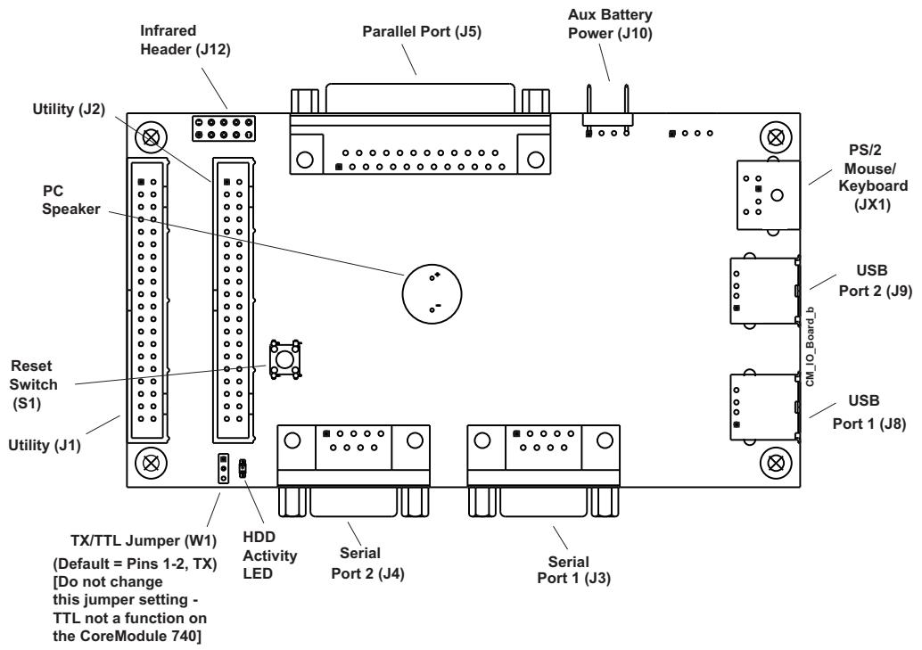
![Infrared Header (J12)\nParallel Port (J5)\nAux Battery Power (J10)\nUtility (J2)\nPC Speaker\nReset Switch (S1)\nUtility (J1)\nTX/TTL Jumper (W1)\n(Default = Pins 1-2, TX)\n(Do not change this jumper setting -\nTTL not a function on the CoreModule 740)\nHDD Activity LED\nSerial Port 2 (J4)\nSerial Port 1 (J3)\nPS/2 Mouse/ Keyboard (JX1)\nUSB Port 2 (J9)\nCM_IO_Board_b\nUSB Port 1 (J8)](.50-1z046-1010-cm740-referencemanual-final-en/5e6b9bb6abf649332388e469ed38144a28d79daadfe6afeec204501c1e2594d7.jpg)

Figure B-1. I/O Interface Board Connectors (Top view)

# NOTE

If you need more information concerning the I/O Interface Board than is provided in this Appendix, refer to the CoreModule 740 QuickDrive for a schematic, BOM, and AVL.

# I/O Interface Board Connectors and Headers

The following tables define the pin signals of all the non-standard connectors and headers on the I/O Interface Board. This appendix does not define industry-standard connectors on the board such as parallel, DB9 serial, PS2 mouse and keyboard, and USB.

NOTE The CoreModule 740 does not support the Infrared header (J12) shown in Figure B-1.

Table B-1 lists the signals and their descriptions for the J1 Utility interface, which provides a shrouded 40-pin header with odd/even (1, 2) pin sequence. The third column in this table denotes the corresponding pins from the J5 header on the CoreModule 740.

Note: The shaded table cells denote power or ground. NC = Not Connected at the CoreModule 740. The \* symbol indicates the signal is Active Low.
Table B-1. Utility Interface Pin Signals (J1)

<table><tr><td>Pin #</td><td>Signal</td><td>From J5 Pin #</td><td>Description</td></tr><tr><td>1</td><td>DCD1*</td><td>J5-1</td><td>Serial Data Carrier Detect 1 – Indicates external modem is detecting a carrier signal (i.e., a communication channel is currently open). In direct connect environments, this input will be driven by DTR1 as part of the DTR1/DSR1 handshake.</td></tr><tr><td>2</td><td>DSR1*</td><td>J5-3</td><td>Serial Data Set Ready 1 – Indicates external serial communications device is powered, initialized, and ready. Used as hardware handshake with DTR1 for overall readiness to communicate.</td></tr><tr><td>3</td><td>RXD1</td><td>J5-5</td><td>Serial Receive Data 1 Input – This line is typically held at a logic 1 (mark) when no data is being transmitted, and is held “Off” for a brief interval after an “On” to “Off” transition on the RTS1 line to allow the transmission to complete.</td></tr><tr><td>4</td><td>RTS1*</td><td>J5-7</td><td>Serial Request To Send 1 – Indicates serial port is ready to transmit data. Used as hardware handshake with CTS1 for low level flow control.</td></tr><tr><td>5</td><td>TXD1</td><td>J5-9</td><td>Serial Transmit Data 1 Output – This line is typically held to a logic 1 when no data is being sent. Typically, a logic 0 (On) must be present on RTS1, CTS1, DSR1, and DTR1 before data can be transmitted on this line.</td></tr><tr><td>6</td><td>CTS1*</td><td>J5-11</td><td>Serial Clear To Send 1 – Indicates external serial communication device is ready to receive data. Used as hardware handshake with RTS1 for low level flow control.</td></tr><tr><td>7</td><td>DTR1*</td><td>J5-13</td><td>Serial Data Terminal Ready 1 – Indicates port is powered, initialized, and ready. Used as hardware handshake with DSR1 for overall readiness to communicate.</td></tr><tr><td>8</td><td>RI1*</td><td>J5-15</td><td>Serial Ring Indicator 1 – Indicates external modem is detecting a ring condition. Used by software to initiate operations to answer and open the communications channel.</td></tr><tr><td>9</td><td>GND</td><td>J5-17</td><td>Digital Ground</td></tr><tr><td>10</td><td>NC</td><td>J5-19</td><td>Not Connected</td></tr><tr><td>11</td><td>DCD2*</td><td>J5-21</td><td>Serial Data Carrier Detect 2 – Indicates external modem is detecting a carrier signal (i.e., a communication channel is currently open). In direct connect environments, this input will be driven by DTR2 as part of the DTR2/DSR2 handshake.</td></tr><tr><td>12</td><td>DSR2*</td><td>J5-23</td><td>Serial Data Set Ready 2 – Indicates external serial communications device is powered, initialized, and ready. Used as hardware handshake with DTR2 for overall readiness to communicate.</td></tr><tr><td>13</td><td>RXD2</td><td>J5-25</td><td>Serial Receive Data 2 Input – This line is typically held at a logic 1 (mark) when no data is being transmitted, and is held “Off” for a brief interval after an “On” to “Off” transition on the RTS2 line to allow the transmission to complete.</td></tr><tr><td>14</td><td>RTS2*</td><td>J5-27</td><td>Serial Request To Send 2 – Indicates serial port is ready to transmit data. Used as hardware handshake with CTS2 for low level flow control.</td></tr><tr><td>15</td><td>TXD2</td><td>J5-29</td><td>Serial Transmit Data 2 Output – This line is typically held to a logic 1 when no data is being sent. Typically, a logic 0 (On) must be present on RTS1, CTS1, DSR1, and DTR1 before transmitting data on this line.</td></tr><tr><td>16</td><td>CTS2*</td><td>J5-31</td><td>Serial Clear To Send 2 – Indicates external serial communication device is ready to receive data. Used as hardware handshake with RTS2 for low level flow control.</td></tr><tr><td>17</td><td>DTR2*</td><td>J5-33</td><td>Serial Data Terminal Ready 2 – Indicates port is powered, initialized, and ready. Used as hardware handshake with DSR2 for overall readiness to communicate.</td></tr><tr><td>18</td><td>RI2*</td><td>J5-35</td><td>Serial Ring Indicator 2 – Indicates external modem is detecting a ring condition. Used by software to initiate operations to answer and open the communications channel.</td></tr><tr><td>19</td><td>GND</td><td>J5-37</td><td>Digital Ground</td></tr><tr><td>20</td><td>TXD2_ TTL (NF)</td><td>J5-39</td><td>Serial Port 2 Transmit TTL – Places TTL TX signals on pin 3 of the Serial Port 2 (J4) when jumper (W1) on I/O Interface Board is set to pins 2-3. (NF = No function at the CoreModule 740.)</td></tr><tr><td>21</td><td>USB_OC0*</td><td>J5-41</td><td>USB0 Over Current Protection – The voltage network monitors power and disables port if this input is low. Direct power input through fuse on I/O Interface Board provides over current protection.</td></tr><tr><td>22</td><td>USB PWR0</td><td>J5-43</td><td>USB Port 0 power (+5V +/-5%)</td></tr><tr><td>23</td><td>USB P0-</td><td>J5-45</td><td>Universal Serial Bus Port 0 Data –</td></tr><tr><td>24</td><td>USB P0+</td><td>J5-47</td><td>Universal Serial Bus Port 0 Data +</td></tr><tr><td>25</td><td>GND</td><td>J5-49</td><td>USB Ground</td></tr><tr><td>26</td><td>USB_OC1*</td><td>J5-51</td><td>USB1 Over Current Protection – The voltage network monitors power and disables port if this input is low. Direct power input through fuse on I/O Interface Board provides over current protection.</td></tr><tr><td>27</td><td>USB PWR1</td><td>J5-53</td><td>USB Port 1 power (+5V +/-5%)</td></tr><tr><td>28</td><td>USB P1-</td><td>J5-55</td><td>Universal Serial Bus Port 1 Data –</td></tr><tr><td>29</td><td>USB P1+</td><td>J5-57</td><td>Universal Serial Bus Port 1 Data +</td></tr><tr><td>30</td><td>GND</td><td>J5-59</td><td>USB Ground</td></tr><tr><td>31</td><td>MS Dta</td><td>J5-61</td><td>Mouse Data</td></tr><tr><td>32</td><td>MS Clk</td><td>J5-63</td><td>Mouse Clock</td></tr><tr><td>33</td><td>GND</td><td>J5-65</td><td>Ground</td></tr><tr><td>34</td><td>MS Pwr</td><td>J5-67</td><td>Mouse Power (+5V +/-5%)</td></tr><tr><td>35</td><td>HD Act</td><td>J5-69</td><td>IDE Hard Drive Activity – Front panel HD activity signal to LEDs</td></tr><tr><td>36</td><td>NC</td><td>J5-71</td><td>Not Connected (External SMI)</td></tr><tr><td>37</td><td>NC</td><td>J5-73</td><td>Not Connected (RS485 Transmit/Receive Data –)</td></tr><tr><td>38</td><td>NC</td><td>J5-75</td><td>Not Connected (RS485 Transmit/Receive Data +)</td></tr><tr><td>39</td><td>NC</td><td>J5-77</td><td>Not Connected (External –12V input)</td></tr><tr><td>40</td><td>NC</td><td>J5-79</td><td>Not Connected (External –5V input)</td></tr></table>

Note: The shaded table cells denote power or ground. NC = Not Connected at the CoreModule 740. The \* symbol indicates the signal is Active Low.
Table B-2 lists the signals and their descriptions for the J2 Utility interface, which provides a shrouded 40-pin header with odd/even (1, 2) pin sequence. The third column in this table denotes the corresponding pins from the J5 header on the CoreModule 740.
Table B-3 lists the signals and their descriptions for the Auxiliary Battery interface which provides a right-angle, single row, 4-pin header (with two pins removed.) The third column in this table denotes the corresponding pins from the on-board J2 header.
Table B-2. Utility Interface Pin Signals (J2)

<table><tr><td>Pin #</td><td>Signal</td><td>From J5 Pin #</td><td>Description</td></tr><tr><td>1</td><td>STB*</td><td>J5-2</td><td>Strobe* – Output used to strobe data into the printer. I/O pin in ECP/EPP mode.</td></tr><tr><td>2</td><td>AFD*</td><td>J5-4</td><td>Auto Feed – This is a Request signal sent to the printer to automatically feed one line after each line is printed.</td></tr><tr><td>3</td><td>PD0</td><td>J5-6</td><td>Parallel Data 0 – These signals (0 to 7) provide the parallel port data to the printer.</td></tr><tr><td>4</td><td>ERR*</td><td>J5-8</td><td>Parallel Error – This is a Status output signal from the printer. A Low State indicates an error condition on the printer.</td></tr><tr><td>5</td><td>PD1</td><td>J5-10</td><td>Parallel Data 1 – Refer to PD0, pin 3, for more information.</td></tr><tr><td>6</td><td>Init*</td><td>J5-12</td><td>Parallel Initialize – This signal used to Initialize printer. Output in standard mode, I/O in ECP/EPP mode.</td></tr><tr><td>7</td><td>PD2</td><td>J5-14</td><td>Parallel Data 2 – Refer to PD0, pin 3, for more information.</td></tr><tr><td>8</td><td>SLIn*</td><td>J5-16</td><td>Parallel Select In – This signal used to select the printer. I/O pin in ECP/EPP mode.</td></tr><tr><td>9</td><td>PD3</td><td>J5-18</td><td>Parallel Data 3 – Refer to PD0, pin 3, for more information.</td></tr><tr><td>10</td><td>GND</td><td>J5-20</td><td>Ground</td></tr><tr><td>11</td><td>PD4</td><td>J5-22</td><td>Parallel Data 4 – Refer to PD0, pin 3, for more information.</td></tr><tr><td>12</td><td>GND</td><td>J5-24</td><td>Ground</td></tr><tr><td>13</td><td>PD5</td><td>J5-26</td><td>Parallel Data 5 – Refer to PD0, pin 3, for more information.</td></tr><tr><td>14</td><td>GND</td><td>J5-28</td><td>Ground</td></tr><tr><td>15</td><td>PD6</td><td>J5-30</td><td>Parallel Data 6 – Refer to PD0, pin 3, for more information.</td></tr><tr><td>16</td><td>GND</td><td>J5-32</td><td>Ground</td></tr><tr><td>17</td><td>PD7</td><td>J5-34</td><td>Parallel Data 7 – Refer to PD0, pin 3, for more information.</td></tr><tr><td>18</td><td>GND</td><td>J5-36</td><td>Ground</td></tr><tr><td>19</td><td>ACK*</td><td>J5-38</td><td>Parallel Acknowledge – This is a Status output signal from the printer. A Low State indicates it has received the data and is ready to accept new data.</td></tr><tr><td>20</td><td>GND</td><td>J5-40</td><td>Ground</td></tr><tr><td>21</td><td>BSY</td><td>J5-42</td><td>Parallel Busy – This is a Status output signal from the printer. A High State indicates the printer is not ready to accept data.</td></tr><tr><td>22</td><td>GND</td><td>J5-44</td><td>Ground</td></tr><tr><td>23</td><td>PE</td><td>J5-46</td><td>Parallel Paper End – This is a Status output signal from the printer. A High State indicates it is out of paper.</td></tr><tr><td>24</td><td>GND</td><td>J5-48</td><td>Ground</td></tr><tr><td>25</td><td>Slct</td><td>J5-50</td><td>Parallel Select – This is a Status output signal from the printer. A High State indicates it is powered on.</td></tr><tr><td>26</td><td>IR FIRM</td><td>J5-52</td><td>IR Function Mode Select – Disabled (Terminated with 10k ohm resistor to ground on CoreModule 740.)</td></tr><tr><td>27</td><td>NC</td><td>J5-54</td><td>Not connected</td></tr><tr><td>28</td><td>GND</td><td>J5-56</td><td>Signal Ground</td></tr><tr><td>29</td><td>IR TXD</td><td>J5-58</td><td>IR Transmit Data (HPSIR or ASKIR)</td></tr><tr><td>30</td><td>IR RXD</td><td>J5-60</td><td>IR Receive Data (HPSIR or ASKIR)</td></tr><tr><td>31</td><td>SPKR+</td><td>J5-62</td><td>Speaker + drive signal</td></tr><tr><td>32</td><td>GND</td><td>J5-64</td><td>Speaker return</td></tr><tr><td>33</td><td>RST SW</td><td>J5-66</td><td>Reset Switch</td></tr><tr><td>34</td><td>KB SW</td><td>J5-68</td><td>Not Connected (Keyboard switch)</td></tr><tr><td>35</td><td>KB DTA</td><td>J5-70</td><td>Keyboard Data signal</td></tr><tr><td>36</td><td>KB CLK</td><td>J5-72</td><td>Keyboard Clock signal</td></tr><tr><td>37</td><td>GND</td><td>J5-74</td><td>Digital Ground</td></tr><tr><td>38</td><td>KB PWR</td><td>J5-76</td><td>Keyboard power (+5V +/-5%)</td></tr><tr><td>39</td><td>BATV+</td><td>J5-78</td><td>External Backup Battery +</td></tr><tr><td>40</td><td>BATV-</td><td>J5-80</td><td>External Backup Battery Return -</td></tr></table>

Table B-3. Auxiliary Battery Interface Pin Signals (J10)

<table><tr><td>Pin #</td><td>Signal</td><td>From On-Board Connector &amp; Pin #</td><td>Description</td></tr><tr><td>1</td><td>BATV+</td><td>J2-39</td><td>External Backup Battery +</td></tr><tr><td>2</td><td>NC</td><td>NA</td><td>Not connected</td></tr><tr><td>3</td><td>NC</td><td>NA</td><td>Not connected</td></tr><tr><td>4</td><td>BATV-</td><td>J2-40</td><td>External Backup Battery Return -</td></tr></table>

Note: The shaded table cells denote power or ground.

# B

Battery
RTC 34

BIOS Setup
accessing BIOS setup (VGA) .... 37
accessing serial console .... 37
splash screen configuration .... 38
Watchdog Timer (WDT) .... 35

BIOS Setup Utility supported features 39

# C

connectors
connector and header list .... 9
pin identification .... 9

console redirection optional feature 34 serial console 34

CoreModule 740
Atom N450 CPU .... 4

block diagram 6

board thickness 11

current capability 33

dimensions 11

features 5

headers and connectors 9

I/O address map 17

low voltage limit 33

major integrated circuits 7

memory map 17

Oops! jumper 34

PC/104 & PC/104-Plus compatibility .... 4

PC/104 Architecture 3

product description 4

see also supported features 4

serial console 34

serial port connections 19

splash screen (OEM Logo) customization .... 38

USB boot 5

USB ports 22

Utility 1 interface 19

voltage requirements 33

Watchdog Timer (WDT) 35

weight 11

CPU fan (optional)
pin-out list .... 33

CPU heatsink
requirements .... 13

# D

dimensions 11

# E

Environmental specifications .... 13

# H

Hot cable console redirection 34 modified serial cable 34 serial console 34

# |

Interrupt (IRQs) list ....16

# J

jumper locations 11

# L

logo screen
requirements ....38

low voltage limit ....33

# O

Oops! jumper
DB9 connector ....34
Serial port 1 ....34

# P

power interface connector ....33
pinouts ....33

power requirements ....13
processor
heatsink requirements ....13

# R

Real Time Clock (RTC) 34

references
PC/104 specifications ....1
PC/104-Plus specifications ....1
PCI 2.2 specifications ....1

# S

Serial console
Hot cable ....34
modified serial cable ....34

serial console
accessing BIOS ....37
see also console redirection ....34
serial terminal ....34
two methods ....34

serial terminal
ANSI-compatible ....34

site preparation
environmental considerations ....13

specifications
PC/104 references ....1
PC/104-Plus references ....1
PCI 2.2 references ....1

splash screen (OEM Logo)
customer defined ....38

supported features
512MB SDRAM ....5
Atom N450 ....5
battery-free boot ....6

console redirection 34

CPU optional fan connector 33

floppy disk drive 5

I/O address map 17

IDE devices 5

IRQ assignments 16

jumpers on-board 11

memory map 17

Oops! jumper (BIOS recovery) ......6, 34

parallel port interface 21

PC/104 bus 5

PC/104-Plus bus 5

PS/2 keyboard and mouse ports ....5, 22

Real Time Clock 5

serial console 6,34

serial interface 19

serial ports 5

soldered SDRAM 5

splash screen 38

USB interface 22

Utility 1 interface .... 19

Watchdog Timer 6

# T

Technical Support
Ask an Expert 47
contact information 47
thermal cooling
processor requirements .... 13

# U

Utility 1 interface
80-pin connector 19
Mouse and Keyboard interface 19
parallel interface 19,21
serial interface 19
USB interface 19

Utility 2 interface
80-pin connector .... 26
Floppy drive interface .... 26
IDE drive interface .... 27

# W

Watchdog Timer (WDT)
functions 35
source code examples 35

web sites
AMI BIOS 8 user's guide .... 1

weight 11
[🔗 Link to the original document](.50-1z046-1010-cm740-referencemanual-final-en/50-1z046-1010-cm740-referencemanual-final-en.pdf)
