# ETX 802

# Computer On Module

# Reference Manual

P/N 5001789A Revision A

# NOTICE

No part of this document may be reproduced, transmitted, transcribed, stored in a retrieval system, or translated into any language or computer language, in any form or by any means, electronic, mechanical, magnetic, optical, chemical, manual, or otherwise, without the prior written permission of Ampro Computers, Incorporated.

# DISCLAIMER

Ampro Computers, Incorporated makes no representations or warranties with respect to the contents of this manual or of the associated Ampro products, and specifically disclaims any implied warranties of merchantability or fitness for any particular purpose. Ampro shall under no circumstances be liable for incidental or consequential damages or related expenses resulting from the use of this product, even if it has been notified of the possibility of such damages. Ampro reserves the right to revise this publication from time to time without obligation to notify any person of such revisions. If errors are found, please contact Ampro at the address listed below on the Notice page of this document.

# TRADEMARKS

Ampro and the Ampro logo are registered trademarks, and CoreModule, EnCore, Little Board, LittleBoard, MightyBoard, MiniModule, ReadyBoard, ReadyBox, ReadyPanel, and ReadySystem are trademarks of Ampro Computers, Inc. All other marks are the property of their respective companies.

REVISION HISTORY

<table><tr><td>Revision</td><td>Reason for Change</td><td>Date</td></tr><tr><td>A, A</td><td>Initial Release</td><td>Aug/06</td></tr><tr><td></td><td></td><td></td></tr><tr><td></td><td></td><td></td></tr><tr><td></td><td></td><td></td></tr><tr><td></td><td></td><td></td></tr><tr><td></td><td></td><td></td></tr><tr><td></td><td></td><td></td></tr></table>

Ampro Computers, Incorporated

5215 Hellyer Avenue

San Jose, CA 95138-1007

Tel. 408 360-0200

Fax 408 360-0222

www.ampro.com

© Copyright 2006, Ampro Computers, Incorporated

# Audience Assumptions

This reference manual is for the person who designs computer related equipment, including but not limited to hardware and software design and implementation of the same. Ampro Computers, Inc. assumes you are qualified in designing and implementing your hardware and its related software into your prototype computer equipment.

# Chapter 1 About This Manual......

Purpose of this Manual .

Reference Material..

Related Ampro Products .. 2

# Chapter 2 Product Overview ....... 5

ETX Computer On Module Concept . .. 5

Product Description... .. 6

Board Features .....

Block Diagram.... . 9

Major Integrated Circuits (ICs) . .. 10

Connector Definitions... ... 11

Jumper Definition ..... .. 12

LED Definitions . .. 12

Specifications .. . 13

Physical Specifications ... 13

Mechanical Specifications.... ... 13

Power Specifications.. .. 14

Environmental Specifications.. ... 14

Thermal/Cooling Requirements . ... 15

# Chapter 3 Hardware.... .. 17

Overview ...... . 17

CPU (U1) .... . 18

Memory ...... . 18

DDR Memory SODIMM Socket (J5) .. .. 18

Flash Memory (U12) .... ... 18

Interrupt Channel Assignments (IRQs). .. 19

Memory Map ...... .. 20

I/O Address Map ...... .. 20

PCI Bus Interface Connector (J1) .. . 21

PCI Bus ..... .. 21

Universal Serial Bus (USB).. .. 25

Serial Interrupt Request . .. 26

Audio Interface.. 26

ISA Bus Interface (J2) .. .. 30

Primary I/O Interface (J3) .. . 35

Floppy Interface .. ... 35

Parallel Interface .... ... 36

Serial Ports 1 and 2 ... .. 37

Infrared (IrDA) Port ... ... 38

PS/2 Keyboard... ... 38

PS/2 Mouse... .. 38

CRT Interface... ... 39

LVDS Interface.. .. 39

IDE and Auxiliary Interface (J4) . . 45

IDE Ports ..... . 45

Ethernet Port Interface .. .. 49

Power Control Signals.. ..50

Power Management Signals ...50

Speaker ... ...50

Real Time Clock (RTC)/Battery.... ...50

SMBus (I2 C Bus)... ...51

Miscellaneous .. ..56

Oops! Jumper (BIOS Recovery).. ..56

Serial Console (Remote Access) . ..56

Temperature Monitoring . .57

Watchdog Timer (WDT).. .57

Power Interface.. .58

Optional CPU Fan (P1)... ..58

Power and Sleep States .... ..58

Power-On Switch.. .58

Sleep States (ACPI) ..... ..58

# Chapter 4 BIOS Setup Utility.............. .....61

Introduction .... ..61

Accessing BIOS Setup Utility (VGA Display) .. ...61

Accessing BIOS Setup Utility (Remote Access) . ..62

BIOS Setup Utility Menus ..... ..63

Main Menu Screen .... ..63

Advanced Menu Screen ...... ..64

PCIPnP (Plug & Play) Menu Screen .... ..73

Boot Menu Screen...... ...76

Security Menu Screen .... ...80

Chipset Menu Screen.... ...82

Power Menu Screen..... ...84

Exit and Defaults Menu Screen.... ...87

# Appendix A Technical Support . ..89

# Appendix B LAN Boot Feature.... .91

Introduction . .91

Accessing PXE Boot Agent BIOS Setup.. ..92

PXE Boot Agent Setup Screen...... ...93

# Index .... ...95

# List of Figures

Figure 2-1. ETX 802 Stacked on Custom Baseboard . ..5

Figure 2-2. Typical Design Flow .. ..6

Figure 2-3. Simplified Functional Block Diagram... .9

Figure 2-4. Component Locations (Top view) . ..10

Figure 2-5. Connector and Component Locations (Bottom view) . ..11

Figure 2-6. Jumper Locations (Top view) . ..12

Figure 2-7. Dimensions (Top, Through Board View).. ..13

Figure 3-1. Oops! Jumper Connection .... ..56

Figure 3-2. Hot Cable Jumper ...... ..56

Figure 4-1. Main Menu Screen ....... ..63

Figure 4-2. Advanced Menu Screen...... ..64

Figure 4-3. PCIPnP Menu Screen .. ..73

Figure 4-4. Boot Menu Screen.. . 76

Figure 4-5. Security Menu Screen ...... . 80

Figure 4-6. Chipset Menu Screen .. . 82

Figure 4-7. Power Menu Screen ... . 84

Figure 4-8. Exit and Defaults Menu Screen .... . 87

Figure B-1. PXE Agent Boot Setup Screen .. . 93

# List of Tables

Table 2-1. Major Integrated Circuit Description and Function . .. 10

Table 2-2. Connector Descriptions... 11

Table 2-3. Jumper Settings ... . 12

Table 2-4. LED Indicators . . 12

Table 2-5. Weight and Footprint Dimensions.. .. 13

Table 2-6. Power Supply Requirements . . 14

Table 2-7. Environmental Requirements .. .. 14

Table 3-1. Interrupt Channel (IRQs) Assignments (Typical).. .. 19

Table 3-2. Memory Map ..... . 20

Table 3-3. I/O Address Map ... . 20

Table 3-4. Simplified PCI Pin/Signal Descriptions (J1).. .. 21

Table 3-5. Simplified USB Interface Pin/Signal Descriptions (J1) .. .. 25

Table 3-6. Simplified Serial Interrupt Request (J1) .. . 26

Table 3-7. Simplified Audio Interface Pin/Signal Descriptions (J1).. . 26

Table 3-8. Complete J1 Interface Pin/Signal Descriptions (J1) ... 27

Table 3-9. Complete J2 ISA Bus Interface Pin/Signal Descriptions (J2) . .. 30

Table 3-10. Simplified Floppy Drive Interface Pin/Signal Descriptions (J3).. .. 35

Table 3-11. Simplified Parallel Interface (SPP) Pin/Signal Descriptions (J3) .. .. 36

Table 3-12. Simplified Serial Interface Pin/Signal Descriptions (J3). . 37

Table 3-13. Simplified Keyboard, Mouse, and Infrared (IrDA) Port Pin/Signal Descriptions (J3)... 39

Table 3-14. Simplified CRT Interface Pin/Signal Descriptions (J3) . .. 39

Table 3-15. Simplified LVDS Interface Pin/Signal Descriptions (J3) . . 39

Table 3-16. Complete J3 Interface Pin/Signal Descriptions (J3) .. .. 41

Table 3-17. Simplified Primary IDE Interface Pin/Signal Descriptions (J4) .. . 45

Table 3-18. Simplified Secondary IDE Interface Pin/Signal Descriptions (J4). .. 47

Table 3-19. Simplified Ethernet Port Pin/Signal Descriptions (J4).. .. 49

Table 3-20. Simplified Power Control and Miscellaneous Pin/Signal Descriptions (J4) .. . 50

Table 3-21. SMBus Reserved Addresses.. .. 51

Table 3-22. Complete J4 Interface Pin/Signal Descriptions (J4) .. . 52

Table 3-23. CPU Fan (P1) .. . 58

Table 4-1. BIOS Setup Utility Menus .. . 62

Table 4-2. Exiting and Loading Default Keys...... . 63

Table 4-3. LCD Panel Type List.. . 83

Table A-1. Technical Support Contact Information ...... . 89

# Purpose of this Manual

This manual is for designers of systems based on the ETX 802 computer on module. This manual contains information that permits designers to create an embedded system based on specific design requirements.

Information provided in this reference manual includes:

• ETX 802 Specifications
• Environmental requirements
• Major integrated circuits (chips) and features implemented
• ETX 802 connector/pin numbers and definition
• BIOS Setup Utility information

Information not provided in this reference manual includes:

• Detailed chip specifications
• Internal component operation
• Internal registers or signal operations
• Bus or signal timing for industry standard busses and signals

# Reference Material

The following list of reference materials may be helpful for you to complete your design successfully. Most of this reference material is also available on the Ampro web site in the Embedded Design Resource Center. The Embedded Design Resource Center was created for embedded system developers to share Ampro’s knowledge, insight, and expertise gained from years of experience.

# Specifications

• ETX Component SBC™ Specification Revision 2.6, 2001
• ETX Component SBC™ Design Guide, Revision 1.5, 2001
For latest revision of the ETX specifications, contact the Working Group, at:
Web site: http://www.etx-ig.org
• PCI 2.2 Compliant Specifications
For latest revision of the PCI specifications, contact the PCI Special Interest Group Office at:
Web site: http://www.pcisig.com

Major Integrated Circuit (Chip) Specifications used on the ETX 802 board:

• Intel® Corporation and the Pentium® M or Celeron® M processors used for the embedded CPU
Web site: http://www.intel.com/design/mobile/datashts/252612.htm = Pentium M
Web site: http://www.intel.com/design/intarch/datashts/301753.htm = Celeron M

• Intel Corporation and the 82855GME and 82801DBM chips used for the Memory Hub/Video controller and I/O Hub respectively.

Web site: http://www.intel.com/design/chipsets/mobile/855gme.htm = Memory Hub

Web site: http://www.intel.com/design/mobile/datashts/252337.htm = I/O Hub

• Standard Microsystems Corp’s chip, LPC47B272, used for the Super I/O controller.

Web site: http://www.smsc.com/main/datasheets/47b27x.pdf

• Realtek Semiconductor, Corp's chip ALC202A, used for the AC'97 Audio CODEC.

Web site: http://www.realtek.com.tw/products/products.aspx

• Intel Corporation and the chip, 82551QM, used for the Ethernet controller.

Web site: http://developer.intel.com/design/network/datashts/82551QM\_DS.htm

• ITE Tech Inc. and the chip, ITE8888G, PCI to ISA Bridge.

Web site: http://www.ite.com.tw/product\_info/PC/Brief-IT8888\_2.asp

# NOTE

If you are unable to locate the datasheets using the links provided, go to the manufacturer's web site where you should be able to perform a search using the chip datasheet number or name listed, including the extension, htm, pdf, etc.

# Related Ampro Products

The following items are directly related to successfully using the Ampro product you have just purchased or plan to purchase. Ampro highly recommends that you purchase and utilize an ETX 802 QuickStart Kit for ease of operation and development.

# ETX 802 Support Products

• ETX 802 QuickStart Kit (QSK)
The QuickStart Kit includes the ETX 802 module, SODIMM, an ETX baseboard, and the ETX 802 Documentation and Support Software (Doc & SW) CD-ROM.
• ETX 802 Documentation and Support Software CD-ROM
The ETX 802 Documentation and Support Software (ETX 802 Doc & SW) CD-ROM is provided with the ETX 802 QuickStart Kit. The CD-ROM includes all of the ETX 802 documentation, including this reference manual and the ETX 802 QuickStart Guide in PDF format, software utilities, board support packages, and drivers for the unique devices used with Ampro supported operating systems.

# Other Ampro ETX Products

ETX 700 – This high-performance, compact, rugged Computer-on-Module (COM) solution uses Intel 650 MHz Low Voltage Celeron or 400 MHz Ultra Low Voltage Celeron CPUs with up to 512 kB Level 2 Cache on board. This ETX module comes with the standard peripherals, including dual Ultra/DMA 33/66/100 IDE, floppy drive interface, PCI bus, ISA bus, serial, parallel, PS/2 keyboard and mouse interfaces, 10/100BaseT Ethernet, USB ports, AGP 4X video interface with up to 32 MB UMA Frame Buffer that supports built-in LVDS at 1600x1200 resolution, and AC’97 sound. It also supports up to 512 MB of SODIMM DRAM on a 50% thicker PCB to meet your custom baseboard needs.

# Other Ampro Products

CoreModule™ Family – These complete embedded-PC subsystems on single PC/104 or PC/104- Plus form-factor (3.6"x3.8") modules feature 486, Celeron, or Celeron M CPUs. Each CoreModule includes a full complement of PC core logic functions, plus disk controllers, and serial and parallel ports. Most modules also include CRT and flat panel graphics controllers and/or an Ethernet interface. The CoreModules also come with built-in extras to meet the critical reliability requirements of embedded applications. These include onboard solid state disk compatibility, watchdog timer, and smart power monitor.
LittleBoard™ Family – These high-performance, highly integrated single-board computers use the EBX form factor (5.75"x8.00"), and are available with the Intel Pentium M, Celeron M, Pentium III, or Celeron processors. The EBX-compliant LittleBoard single-board computers offer functions equivalent to a complete laptop or desktop PC system, plus several expansion cards. Built-in extras to meet the critical requirements of embedded applications include onboard solid state disk capability, watchdog timer, and smart power monitor.
MightyBoard™ Family – These low-cost, high-performance single-board computers (SBC) use the Mini-ITX form factor (6.75"x 6.75") and are available with Intel Celeron M or Pentium M processors. MightyBoard products offer the equivalent functions of a complete laptop or desktop PC system, including DDR memory, high performance graphics, USB 2.0, Gigabit Ethernet, plus standard PCI expansion capability in one card slot.
MiniModule™ Family – This line of peripheral interface modules, compliant with PC/104, PC/104-Plus, and/or PCI-104 form factor (3.6"x3.8") standards can be used with Ampro’s CoreModule, LittleBoard, and ReadyBoard single board computers (SBCs) to expand the I/O configuration of embedded systems. Ampro's highly reliable MiniModule products add value to existing designs by adding I/O ports, such as IEEE 1394 (FireWire), or by adding support for legacy boards, such as a PCI to ISA bridge adapter board.
ReadyBoard™ Family – These low-cost, high-performance single-board computers (SBC) use the EPIC form factor (4.5"x6.5") and are available with the Intel Pentium III, Celeron, Pentium M and Celeron M processors. ReadyBoard products offer functions equivalent to a complete laptop or desktop PC system with standard PC-style connections, and features such as DDR or DDR2 memory, high performance graphics, USB 2.0, Ethernet and Gigabit Ethernet ports, AC'97 Audio, plus several expansion cards. Ampro also includes such features as watchdog timer, battery-free boot, a customizable splash screen, Oops! jumper (BIOS recovery), and serial console.

This introduction presents general information about the ETX Architecture and the ETX 802 Computer On Module (COM). After reading this chapter you should understand:

• ETX Computer On Module concept
• ETX 802 architecture
• ETX 802 features
• Major components
• Connectors
• Specifications

# ETX Computer On Module Concept

Embedded system designers face increasing pressure to bring products to market quickly. Many products that once incorporated a custom CPU design can no longer afford the time to develop and debug a custom CPU let alone port operating system software to it. Furthermore, CPU subsystem design usually plays a small part in providing any uniqueness to an embedded product. The remainder of the embedded product design adds key logic elements that provide a unique product and differentiate it from other products serving the same market. The challenge is to speed these designs to market by eliminating the need for a custom CPU design while providing the flexibility to include all critical elements, which make the embedded product unique.

The Embedded Technology eXtended (ETX) module provides an off-the-shelf CPU subsystem that can be included in virtually any embedded system. ETX modules work like a high-integration chip, plugging into your custom circuit board design to provide specific control for your logic application. See Figure 2-1.

![The diagram depicts an assembly of modules and a baseboard with the following labeled blocks and connections:\n\n*   **Top Section:** The text '**M2.5 Screws (4)**' points to two T-shaped screw icons. Centered on a horizontal rail is a grey block labeled '**ETX 802 Module**'.\n*   **Middle Connections:** Two large black arrows point downward from the rail towards the baseboard area below.\n*   **Bottom Section:** The text '**Custom Baseboard Design**' is centered at the bottom.\n*   **Left Side Connection:** The text '**M2.5 PEM Nuts Spacing 3mm (4)**' has a line pointing to small mounting posts on the left side of the baseboard.\n*   **Right Side Connection:** The text '**Stack Connectors (4 pairs)**' has a line pointing to small mounting posts on the right side of the baseboard.\n*   **Far Right Edge:** Vertical text reads '**ETX802stack**'.](.5001789aa-etx802refman/1ceed357c40c43bf9a2f436781a43d5b786ce299b09d5dd3bb65be9f9ff60fe8.jpg)

Figure 2-1. ETX 802 Stacked on Custom Baseboard

ETX provides a simple, standard interface that is independent of CPU type. The ETX interface includes the industry-standard PCI bus, ISA bus, I/O signals from the peripheral components on the ETX module, power, and ground. The ETX modules support Intel architecture (x86) processors. Go to the Ampro web site (www.ampro.com) for the latest ETX processor support information.

The standard ETX interface lets you try different processors and different processor types in your actual product environment with the ability to defer a processor choice until late in the project if you so choose. The interface also lets you easily offer different versions of your product with different capabilities by either selecting different ETX modules with the same baseboard, or by designing different baseboards for the same CPU. This simple ability to upgrade by either selecting a more powerful CPU (without baseboard redesign) or enhancing the baseboard without touching the CPU subsystem or the bulk of the applications software.

The ETX flexibility enables designers to take an accelerated, low risk path with proven ETX module designs. Your design flow might look similar to the one shown in Figure 2-2. This diagram gives a Typical Design Flow of hardware and software functions.

![This flowchart depicts two parallel design processes that converge into a final integration step.\n\n**Left Side: Hardware Design Path**\nThe left column is labeled 'Hardware Design Path' and features a large gray arrow pointing downward. The blocks within this path, in sequential order from top to bottom, are:\n1.  **Design application-specific baseboard**\n2.  **Fabricate baseboard**\n3.  **Debug baseboard**\n4.  **Revise baseboard if necessary**\n\n**Right Side: CPU and Software Design Path**\nThe right column is labeled 'CPU and Software Design Path' and features a large gray arrow pointing downward. The blocks within this path, in sequential order from top to bottom, are:\n1.  **Select CPU**\n2.  **Select OS & Tools**\n3.  **Write and Test Application Code**\n4.  **Write drivers for custom Logic**\n\n**Convergence**\nBoth large gray arrows originate at the top of their respective columns and converge at the bottom, pointing toward a single final block centered at the bottom of the diagram labeled:\n*   **Integrate application code**](.5001789aa-etx802refman/a0e6574783d7fff4e79a050fea1dec15cf16b646fd6fadadbae058222a24c22e.jpg)

Figure 2-2. Typical Design Flow

# Product Description

The ETX 802 is an exceptionally high integration, high performance, rugged, and high quality Computer-on-Module (COM), which contains all the component subsystems of an ATX motherboard plus the equivalent of up to 2 expansion boards. The ETX 802 is based on one of the ultra high performance, high-integration Intel Pentium M or Celeron M processors, and gives designers the choice of a complete, high performance, rugged, embedded processor based on the ETX form factor that conforms to the ETX V2.7 specification. The module plugs into a custom baseboard, which has connectors and additional circuitry to meet your application requirements.

Each ETX 802 incorporates an Intel® 855GME chipset (82855GME + 82801DBM) for the Memory and Graphics Hub (Northbridge) and I/O Hub (Southbridge) controllers. This includes the Intel 82855GME Memory and Graphics Hub (Northbridge), which controls graphics and memory interface and the Intel 82801DBM I/O Hub (Southbridge) Controller for some I/O functions. A Super I/O chip by Standard Microsystems Corp. provides most of the I/O functions including a PCI to ISA Bridge chip for ISA functions. Together these chips provide two Ultra/DMA 33/66/100 IDE controllers supporting two IDE drives each, floppy, four USB 2.0 ports, two serial ports, an EPP/ECP parallel port, PS/2 keyboard and mouse interfaces, and an audio AC’97 controller on the module. The ETX 802 also supports an Ethernet controller (10/100BaseT), up to 1 GB of DDR RAM in a single 200-pin DDR SODIMM socket, and a 128-bit graphics controller, which provides CRT (VGA) and flat panel video interfaces.

The ETX 802 is particularly well suited to either embedded or portable applications and meets the size, power consumption, temperature range, quality, and reliability demands of embedded system applications. The ETX 802 requires a single +5V power supply.

# Board Features

# • CPU features

1.4 GHz Low Voltage (LV) Intel Pentium® M 738 (with 2 MB L2 cache), 1.0 GHz Ultra Low Voltage (ULV) Celeron® M 373 (with 512 kB L2 cache), or 800 MHz ULV Celeron M (with 0 kB L2 cache) processors
♦ All processors support a Front Side Bus (FSB) of 400 MHz

# • Memory

♦ Provides a single 200-pin DDR SODIMM socket
♦ Supports a single +2.5V DDR RAM SODIMM up to 1 GB
♦ Supports PC2700 DDR 333 (166 MHz)

# • PCI Bus/ISA Bus

♦ PCI 2.2 compliant, 32-bits wide
♦ Supports PCI Bus speed at 33 MHz
♦ Supports ISA bus speed at 8 MHz

# • IDE Interfaces

♦ Supports two enhanced IDE controllers (4 devices)
♦ Supports dual bus master mode
♦ Supports Ultra DMA 33/66/100 modes
♦ Supports ATAPI and DVD peripherals
♦ Supports IDE native and ATA compatibility modes

# • Floppy Disk Interface

♦ Supports shared output connector with Parallel port
♦ Supports two floppy drives
♦ Supports all standard PC/AT formats: 360 kB, 1.2 MB, 720 kB, 1.44 MB, and 2.88 MB

# • Serial Ports

♦ Provides two buffered TTL serial ports with full handshaking (transceivers on baseboard)
♦ Provides two 16550-equivalent controllers, each with a built-in 16-byte FIFO buffer
♦ Provides programmable word length, stop bits, and parity
♦ Provides 16-bit programmable baud-rate generator
♦ Provides full modem capability

# • Infrared Interface

♦ Provides a single IrDA 1.1 port
♦ Supports HPSIR and ASKIR infrared modes

# • Parallel Port

♦ Supports shared output connector with Floppy controller
♦ Supports standard 25-pin printer (LPT1) port
♦ Supports IEEE standard 1284 protocols of EPP and ECP outputs
♦ Bi-directional data lines

♦ Supports 16 byte FIFO for ECP mode.

• USB Ports

♦ Supports two root USB hubs
♦ Supports four USB ports
♦ Supports USB v2.0 and legacy v1.1
♦ Supports over-current fuses on baseboard
♦ Supports USB Boot and the respective USB Boot devices

• Keyboard/Mouse Interface

♦ Supports PS/2 keyboard
♦ Supports PS/2 mouse

• Audio Interface

♦ Supports AC’97 standard
♦ Provides AC’97 CODEC onboard
♦ Supports an audio amplifier on baseboard

Ethernet Interface

♦ Provides an Intel 82551QM Controller and one Ethernet port
♦ Supports LAN Boot (See Appendix B)
♦ Supports magnetics and RJ45 connector on baseboard
♦ Supports IEEE 802.3 10BaseT/100BaseTX compatible physical layer
♦ Supports Auto-negotiation for speed and duplex mode
♦ Supports full duplex or half-duplex mode

• Full-duplex mode supports transmit and receive frames simultaneously
• Supports IEEE 802.3x Flow control in full duplex mode
• Half-duplex mode supports enhance proprietary collision reduction mode

• Video Interfaces (CRT/LVDS)

♦ Supports CRT (1600 x 1200) with 64 MB UMA (Unified Memory Architecture)
♦ Provides integrated 128-bit graphics controller
♦ Provides LVDS outputs (1 or 2 channel)

• Miscellaneous

♦ Provides a Real-Time Clock (RTC)
♦ Supports battery-free boot
♦ Supports an external battery for Real-Time Clock operation
♦ Supports a Oops! Jumper (BIOS recovery)
♦ Supports Remote Access function (Serial Console or Console Redirection)
♦ Provides Watchdog Timer feature
♦ Supports a customizable Splash Screen (OEM boot logo)
♦ Supports Power Management (ACPI 2.0, including S3 suspend-to-RAM)

# Block Diagram

Figure 2-3 shows the functional components of the board.
![This block diagram illustrates the system architecture of an ETX 802 motherboard.\n\n**Central Processing and Memory**\n*   **Intel Pentium M or Celeron M CPU** connects bidirectionally to **Memory Hub 82855GME (Northbridge)**.\n*   **Clock** connects to **Intel Pentium M or Celeron M CPU**, **Memory Hub 82855GME (Northbridge)**, and **DDR SODIMM**. **Clock** connects bidirectionally to **Temp**.\n*   **Memory Hub 82855GME (Northbridge)** connects bidirectionally to **CRT, LVDS** (which connects to **J3(X3)**) and to **DDR SODIMM** via **Memory Bus**.\n\n**Hub Interface and SMBus**\n*   **Memory Hub 82855GME (Northbridge)** connects to **I/O Hub 82801DBM (Southbridge)** via **Hub Interface**.\n*   **I/O Hub 82801DBM (Southbridge)** connects to **Memory Hub 82855GME (Northbridge)** and **DDR SODIMM** via **SMBus**.\n\n**Southbridge and Connected Peripherals**\n*   **I/O Hub 82801DBM (Southbridge)** connects bidirectionally to **512kB ROM BIOS**.\n*   **I/O Hub 82801DBM (Southbridge)** connects bidirectionally to **J1(X1)** via **AC'97 Link**.\n*   **I/O Hub 82801DBM (Southbridge)** connects bidirectionally to **J1(X1)** via **PCI Bus**.\n*   **I/O Hub 82801DBM (Southbridge)** connects to **PATA**, which connects to **IDE Primary** and **IDE Secondary** (both connecting to **J4(X4)**).\n*   **I/O Hub 82801DBM (Southbridge)** connects to **USB**, which connects to **USB Port 1**, **USB Port 2**, **USB Port 3**, and **USB Port 4** (all connecting to **J1(X1)**).\n\n**PCI Bus Network**\n*   **PCI Bus** connects **I/O Hub 82801DBM (Southbridge)** to:\n    *   **Ethernet Controller 82251QM** (which connects to **J4(X4)**).\n    *   **Super I/O LPC47B272**.\n    *   **PCI/ISA Bridge ITE8888G** (which connects to **ISA**, connecting to **J2(X2)**).\n\n**Super I/O and Local Peripherals**\n*   **Super I/O LPC47B272** connects bidirectionally to **IrDA 1.1**, **Floppy/Parallel**, **Keyboard, Mouse**, **COM1**, **COM2**, and **J3(X3)**.\n\n**Connectors**\n*   **J1(X1)** connects to **AC'97 Link**, **PCI Bus**, and **USB Port 1-4**.\n*   **J2(X2)** connects to **ISA**.\n*   **J3(X3)** connects to **CRT, LVDS** and **Super I/O LPC47B272**.\n*   **J4(X4)** connects to **Ethernet Controller 82251QM** and **IDE Primary/Secondary**.\n*   The bottom legend lists **ETX 802 Connectors** (**J1**, **J2**, **J3**, **J4**) and **Baseboard Connectors** (**X1**, **X2**, **X3**, **X4**).](.5001789aa-etx802refman/7ae7047ebc3596c6a0b12f7331542dc4681fe338dd683d1b87f53965881d5092.jpg)

Figure 2-3. Simplified Functional Block Diagram

# Major Integrated Circuits (ICs)

Table 2-1 lists the major integrated circuits (chips), including a brief description, on the ETX 802 module and Figures 2-4 and 2-5 show the location of the major chips.

Table 2-1. Major Integrated Circuit Description and Function

<table><tr><td>Chip Type</td><td>Mfg.</td><td>Model</td><td>Description</td><td>Function</td></tr><tr><td>CPU (U1)</td><td>Intel</td><td>Pentium M Celeron M</td><td>LV 1.4 GHz, ULV 1.0 GHz, or ULV 800 MHz CPU&#x27;s</td><td>Embedded CPU</td></tr><tr><td>Memory Hub (U2)</td><td>Intel</td><td>82855GME</td><td>Provides Memory control and Video functions</td><td>Memory and Video</td></tr><tr><td>I/O Hub (U8)</td><td>Intel</td><td>82801DBM</td><td>Provides some of standard I/O functions</td><td>Some I/O Functions</td></tr><tr><td>Super I/O (U13)</td><td>Standard Microsystems Corp.</td><td>LPC47B272</td><td>Provides the remaining I/O functions</td><td>Most I/O Functions</td></tr><tr><td>Audio CODEC (U9)</td><td>RealTek</td><td>ALC202A</td><td>Provides audio component functions</td><td>Audio Functions</td></tr><tr><td>Ethernet Controller (U10)</td><td>Intel</td><td>82551QM</td><td>Provides 10/100BaseT Ethernet controller</td><td>Ethernet Functions</td></tr><tr><td>PCI/ISA Bridge (U33)</td><td>ITE Tech Inc.</td><td>ITE8888G</td><td>Provides bridging of PCI and ISA busses</td><td>PCI/ISA Bridge</td></tr></table>

![CPU (U1)\nGraphics &\nMemory Hub\n(U2)\n(Northbridge)\nVoltage\nControl\nCircuitry\nFlash (U12)\nSuper I/O (U13)\nDDR SODIMM\n(Phantom Image)\nClock (U14)\nETX802RfM_01a\nJp2\nJp1\nU1\nU2\nU3\nU4\nU5\nU6\nL10\nQ16\nU29\nU36\nU28\nU12\nU13\nS3 Mode\nY7\nY4\nL9\nL8\nL7\nD11\nD10\nP1](.5001789aa-etx802refman/55a8f74b9e1b1b5464ac3d417eb667f10906613f6ca809f07cca74f892c74bf3.jpg)

Figure 2-4. Component Locations (Top view)

# Connector Definitions

Table 2-2 describes the connectors shown in Figures 2-4 and 2-5.

Table 2-2. Connector Descriptions

<table><tr><td>No.</td><td>Signals</td><td>Description</td></tr><tr><td>P1</td><td>CPU Fan connector</td><td>3-pin header provides +5V, Fan Tachometer, and ground to fan</td></tr><tr><td>J1</td><td>PCI, USB, Audio</td><td>100-pin connector for 32-bit PCI, USB (4 ports), and Audio</td></tr><tr><td>J2</td><td>ISA Bus</td><td>100-pin connector for ISA bus</td></tr><tr><td>J3</td><td>Video, I/O</td><td>100-pin connector for Video (VGA, LVDS) and I/O(Floppy/Parallel, Serial Ports 1 &amp; 2, and Infrared) signals</td></tr><tr><td>J4</td><td>IDE, Ethernet</td><td>100-pin connector for IDE (Primary &amp; Secondary IDE),  $I^{2}C$  bus, Power Management, and the Ethernet port</td></tr><tr><td>J5</td><td>DDR Memory</td><td>200-pin socket for a RAM SODIMM</td></tr></table>

![PCI, USB, Audio (J1)\nISA Bus (J2)\nAudio\nCODEC\n(U9)\nU9\nU21\nQ8\nQ7\nQ12\nQ13\nY2\nU10\nQ10 Q15\nU24\nPCI to ISA\nBridge\n(U33)\nU33\nVideo, I/O (J3)\nIDE, Ethernet (J4)\nThermal\nMonitor\n(U30)\nJ3\nJ4\nETX802RfM_02a](.5001789aa-etx802refman/fd2efc3ef3bc235e73289d43b7fc4fec2f8f3f2550924dc3864a12947f8121b9.jpg)

Figure 2-5. Connector and Component Locations (Bottom view)

# Jumper Definition

Table 2-3 describes the jumpers shown in Figure 2-6.
Table 2-3. Jumper Settings

<table><tr><td>Jumper #</td><td>Installed</td><td>Removed/Enabled</td></tr><tr><td>JP1 – AT/ATX Power Select</td><td>AT, or +5 Volt only (pins 1-2)</td><td>ATX Operation (Removed) Default</td></tr><tr><td>JP2 – CMOS Normal/Clear</td><td>Clear (pins 1-2)</td><td>Normal (Removed) Default</td></tr></table>

![AT/ATX Power Supply Select (JP1)\nJP1\nU28\nU29\nU36\nQ16\nL10\nS3 Mode LED (D17)\nD17\nU12\nU2\nU13\nCP\nCMOS Normal/ Clear (JP2)\nJP2\nL7\nD16\nL8\nL9\nL6\nL5\nD10\nPower LED (D10)\nCPU Fan (P1)\nP1\nU4\nJ5\nDDR SODIMM Socket (J5)\nETX802RfM_01b](.5001789aa-etx802refman/9fc160fa63406bb88f4fc499b337d3e1ae7be36f9ad4e2876aaa4e9a97ba4f81.jpg)

Figure 2-6. Jumper Locations (Top view)

# LED Definitions

Table 2-4 provides the definition of the LED located on the ETX 802 board. Refer to Figure 2-6.
Table 2-4. LED Indicators

<table><tr><td>Indicator</td><td>On State</td><td>Off State</td></tr><tr><td>Power Indicator (D10)</td><td>Steady Green = Power On</td><td>Steady Off = Power Off</td></tr><tr><td>S3 Mode (D17)</td><td>Steady Yellow = In S3 (suspend to RAM) mode</td><td>Steady Off = Not in S3 state</td></tr></table>

Note: The ETX 802's power LED also indicates there is power to the baseboard, when the green LED (D10) is brightly lit.

# Specifications

# Physical Specifications

Table 2-5 gives the physical dimensions of the board and Figure 2-7 gives the mounting dimensions.

Table 2-5. Weight and Footprint Dimensions

<table><tr><td>Item</td><td>Dimension</td></tr><tr><td>Weight</td><td>0.11 kg. (0.243lbs.)w SODIMM,w/o heatsinks</td></tr><tr><td>Height (overall)</td><td>5.29 mm (0.208&quot;)</td></tr><tr><td>Width</td><td>95 mm (3.74&quot;)</td></tr><tr><td>Length</td><td>114 mm (4.48&quot;)</td></tr><tr><td>Thickness</td><td>2.36 mm (0.093&quot;)</td></tr></table>

<table><tr><td>NOTE</td><td>Overall height is measured from the upper board surface to the highest permanent component (SODIMM socket, J5) on the upper board surface. This measurement does not include the heatsinks available for this board or the various sizes of SODIMM inserted into the socket. The heatsinks will increase this dimension.</td></tr></table>

# Mechanical Specifications

Figure 2-7 provides a through the board view of the ETX 802 with the mechanical mounting dimensions.
![| Label | Dimension (mm) |\n|-------|----------------|\n| J1    | 9.2            |\n| J2    | 85.0           |\n| J3    | 50.8           |\n| J4    | 43.4           |](.5001789aa-etx802refman/802b8f029e1e455e26ad7c343477712952875c96a25c55f3c65b1e9a65312531.jpg)

Figure 2-7. Dimensions (Top, Through Board View)

<table><tr><td>NOTE</td><td>All dimensions are given in millimeters and all dimensions without tolerance are +/-0.2 mm.</td></tr></table>

# Power Specifications

Table 2-6 shows the power requirements from the baseboard and the board power output.

Table 2-6. Power Supply Requirements

<table><tr><td>Parameter</td><td>800 MHz ULV Celeron M Characteristics</td><td>1.0 GHz ULV Celeron M Characteristics</td><td>1.4 GHz LV Pentium M Characteristics</td></tr><tr><td>Input Type</td><td>Regulated DC voltages</td><td>Regulated DC voltages</td><td>Regulated DC voltages</td></tr><tr><td>In-rush Current*</td><td>14.24 Amps</td><td>14.24 Amps</td><td>14.24 Amps</td></tr><tr><td>Typical BIT**Current (W)</td><td>2.68 Amps (13.41W)</td><td>2.75 Amps (13.73W)</td><td>3.34 Amps (16.68W)</td></tr></table>

Notes: \*The In-rush current represents video, 128 MB RAM, and power only connected through the Ampro baseboard. Typically, in-rush current reflects the short duration current spike associated with charging large on-board bulk capacitance during power supply start up. However, the listed in-rush current value is the result of placing a switch on the DC output of a fully 'ramped' power supply to give a worst-case current value, which is much higher than the standard method. This in-rush value should be regarded as a maximum design guideline, not a requisite value.

\*\*The Burn-In-Test (BIT) current setup has CRT video, 128 MB RAM, floppy drive (1), IDE hard disk drive (1), USB hard disk drive (1), USB CD-ROM (1), serial ports (2) with loopbacks, keyboard, mouse, compact flash card (64 MB) installed on baseboard (1), USB compact flash card reader with compact flash card (64 MB) installed (1), USB Jump-drive (1), and the Ethernet port (1) operating under Microsoft® Windows® XP (SP2). Since the ETX 802 can not operate without a baseboard, all current measurements include the Ampro baseboard in the QuickStart Kit.

# Environmental Specifications

Table 2-7 provides the most efficient operating and storage condition ranges required for this board.

Table 2-7. Environmental Requirements

<table><tr><td>Parameter</td><td>800 MHz ULVCeleron M Conditions</td><td>1.0 GHz ULVCeleron M Conditions</td><td>1.4 GHz LVPentium M Conditions</td></tr><tr><td colspan="4">Temperature</td></tr><tr><td>Operating</td><td>-20° to +70°C(-4° to +158°F)</td><td>-20° to +70°C(-4° to +158°F)</td><td>-20° to +70°C(-4° to +158°F)</td></tr><tr><td>Extended(Optional)</td><td>-40° to +85°C(-40° to +185°F)</td><td>-40° to +85°C(-40° to +185°F)</td><td>-40° to +85°C(-40° to +185°F)</td></tr><tr><td>Storage</td><td>-55° to +85°C(-67° to +185°F)</td><td>-55° to +85°C(-67° to +185°F)</td><td>-55° to +85°C(-67° to +185°F)</td></tr><tr><td colspan="4">Humidity</td></tr><tr><td>Operating</td><td>5% to 95%relative humidity,non-condensing</td><td>5% to 95%relative humidity,non-condensing</td><td>5% to 95%relative humidity,non-condensing</td></tr><tr><td>Non-operating</td><td>5% to 95%relative humidity,non-condensing</td><td>5% to 95%relative humidity,non-condensing</td><td>5% to 95%relative humidity,non-condensing</td></tr></table>

# Thermal/Cooling Requirements

The CPU, Memory Hub, I/O Hub, and voltage regulators are the main sources of heat on the board. The ETX 802 is designed to operate at its maximum CPU speed of 800 MHz, 1.0 GHz, or 1.4 GHz. The CPUs and Memory & Graphics Hub (Northbridge) require a heatsink, but no fan below + 70°C. However, the 1.4 GHz Pentium M requires a fan above + 70°C. Thermal sensors are provided on the ETX 802 and an optional heatspreader plate is also available.

# NOTE

If you use Ampro's optional heatspreader plate, you must provide an additional form of cooling, such as a fan. A heatspreader plate should not be considered a complete thermal solution for any of the processors listed above, especially the 1.4 GHz Pentium M CPU.

# Overview

This chapter discusses the chips and features of the connectors in the following order:

• CPU (U1)
• Memory (J5)
• PCI Bus Interface (J1)
♦ USB ♦ Audio Interface

• ISA Bus Interface (J2)

• Primary I/O Interface (J3)

♦ Floppy/Parallel Interface
♦ Serial Port Interfaces
♦ Keyboard
♦ Mouse
♦ Infrared (IrDA)
♦ Video Interfaces (CRT & LVDS)

• IDE and Auxiliary Interface (J4)

♦ Primary IDE Interface
♦ Secondary IDE Interface
♦ Ethernet Interface
♦ Time of Day (RTC)/Battery
♦ Speaker
♦ Power Control and Management
♦ SMBus

• Miscellaneous

♦ Oops! Jumper (BIOS recovery)
♦ Remote Access (Serial Console)
♦ Temperature Monitoring
♦ Watchdog timer (WDT)
♦ Power Interface (including ACPI)

# NOTE

Ampro Computers, Inc. only supports the features/options tested and listed in this manual. The main integrated circuits (chips) used in the ETX 802 may provide more features or options than are listed for the ETX 802, but some of these chip features/options are not supported on the board and will not function as specified in the chip documentation.

# CPU (U1)

The ETX 802 supports three Intel processor choices; high performance Low Voltage (LV) 1.4 GHz Pentium® M 738, Ultra Low Voltage (ULV) 1.0 GHz Celeron® M 373, or a ULV 800 MHz Celeron M processor.

# Celeron M Processors

The 800 MHz Celeron M processor (Dothan core) has 0 kB L2 Cache on board, with a 400 MHz FSB (front side bus). This Celeron M processor uses 90 nm architecture and requires a heatsink, but no fan.

The 1.0 GHz Celeron M 373 processor (Dothan core) has 512 kB L2 Cache on board with a 400 MHz FSB. This Celeron M 373 processor uses 90 nm architecture and requires a heatsink, but no fan.

# Pentium M Processor

The 1.4 GHz Pentium M 738 processor (Dothan core) has 2 MB L2 Cache on board with a 400 MHz FSB. This Pentium M 738 processor uses 90 nm architecture and requires a heatsink, but no fan below + 70°C. For the extended temperature range (+70°C to +85°C) a fan is required.

# CAUTION

To prevent processor overheating, you must provide a heatsink on the CPU. If you use an optional heatspreader, you must provide an additional form of cooling, such as a fan. The heatspreader is not a complete thermal solution for any of the processors listed.

# Memory

The ETX 802 memory consists of the following elements:

• DDR RAM SODIMM
• Flash memory

# DDR Memory SODIMM Socket (J5)

The ETX 802 supports a single 200-pin DDR SODIMM socket.

• DDR SODIMM socket can support up to 1 GB of memory
• Supports +2.5V, PC2700 DDR 333 (333 Mbps, 166 MHz (6 ns))

# NOTE

Ampro recommends using PC2700 DDR 333 (333 Mbps, 166 MHz, 6 ns), +2.5V, 200-pin, DDR RAM SODIMM for maximum performance. The ETX 802 will operate acceptably with a PC2100 DDR 266 (266 Mbps, 133 MHz, 7.5 ns) SODIMM.

# Flash Memory (U12)

There is an 8-bit wide, 512 kB flash device used for system BIOS and is connected to the I/O Hub (82801DBM), through an LPC bus transceiver. The flash memory is used to store system parameters and can be used for battery-free boot capability when there is no battery present. The BIOS is reprogrammable and the features supported are detailed in Chapter 4, BIOS Setup Utility.

# Interrupt Channel Assignments (IRQs)

The channel interrupt assignments are listed in Table 3-1.

Table 3-1. Interrupt Channel (IRQs) Assignments (Typical)

<table><tr><td>Device vs IRQ No.</td><td>0</td><td>1</td><td>2</td><td>3</td><td>4</td><td>5</td><td>6</td><td>7</td><td>8</td><td>9</td><td>10</td><td>11</td><td>12</td><td>13</td><td>14</td><td>15</td></tr><tr><td>Timer</td><td>X</td><td></td><td></td><td></td><td></td><td></td><td></td><td></td><td></td><td></td><td></td><td></td><td></td><td></td><td></td><td></td></tr><tr><td>Keyboard</td><td></td><td>X</td><td></td><td></td><td></td><td></td><td></td><td></td><td></td><td></td><td></td><td></td><td></td><td></td><td></td><td></td></tr><tr><td>Secondary Cascade</td><td></td><td></td><td>X</td><td></td><td></td><td></td><td></td><td></td><td></td><td></td><td></td><td></td><td></td><td></td><td></td><td></td></tr><tr><td>COM1</td><td></td><td></td><td></td><td>O</td><td>D</td><td></td><td></td><td></td><td></td><td></td><td></td><td></td><td></td><td></td><td></td><td></td></tr><tr><td>COM2</td><td></td><td></td><td></td><td>D</td><td>O</td><td></td><td></td><td></td><td></td><td></td><td></td><td></td><td></td><td></td><td></td><td></td></tr><tr><td>Floppy</td><td></td><td></td><td></td><td></td><td></td><td></td><td>X</td><td></td><td></td><td></td><td></td><td></td><td></td><td></td><td></td><td></td></tr><tr><td>Parallel</td><td></td><td></td><td></td><td></td><td></td><td>O</td><td></td><td>D</td><td></td><td></td><td></td><td></td><td></td><td></td><td></td><td></td></tr><tr><td>RTC</td><td></td><td></td><td></td><td></td><td></td><td></td><td></td><td></td><td>X</td><td></td><td></td><td></td><td></td><td></td><td></td><td></td></tr><tr><td>IDE Primary</td><td></td><td></td><td></td><td></td><td></td><td></td><td></td><td></td><td></td><td></td><td></td><td></td><td></td><td></td><td>D</td><td>O</td></tr><tr><td>IDE Secondary</td><td></td><td></td><td></td><td></td><td></td><td></td><td></td><td></td><td></td><td></td><td></td><td></td><td></td><td></td><td>O</td><td>D</td></tr><tr><td>Math Coprocessor</td><td></td><td></td><td></td><td></td><td></td><td></td><td></td><td></td><td></td><td></td><td></td><td></td><td></td><td>X</td><td></td><td></td></tr><tr><td>PS/2 Mouse</td><td></td><td></td><td></td><td></td><td></td><td></td><td></td><td></td><td></td><td></td><td></td><td></td><td>X</td><td></td><td></td><td></td></tr><tr><td>AC&#x27;97 CODEC</td><td></td><td></td><td></td><td></td><td></td><td>D</td><td></td><td>O</td><td></td><td>O</td><td>O</td><td></td><td></td><td></td><td></td><td></td></tr><tr><td>PCI INTA</td><td colspan="16">Automatically Assigned or User selectable</td></tr><tr><td>PCI INTB</td><td colspan="16">Automatically Assigned or User selectable</td></tr><tr><td>PCI INTC</td><td colspan="16">Automatically Assigned or User selectable</td></tr><tr><td>PCI INTD</td><td colspan="16">Automatically Assigned or User selectable</td></tr><tr><td>USB</td><td colspan="16">Automatically Assigned</td></tr><tr><td>VGA</td><td colspan="16">Automatically Assigned</td></tr><tr><td>Ethernet</td><td colspan="16">Automatically Assigned</td></tr></table>

Legend: D = Default, O = Optional, X = Fixed Refer also to the IRQs listed in Chapter 4, BIOS Setup.

<table><tr><td>NOTE</td><td>The IRQs for the Ethernet, Video, and Internal LPC bus are automatically assigned by the BIOS Plug and Play logic.</td></tr></table>

# Memory Map

This table provides the common PC/AT memory allocations. BIOS uses memory below 000500h.

Table 3-2. Memory Map

<table><tr><td>Base Address</td><td>Function</td></tr><tr><td>00000000h - 0009FFFFh</td><td>Conventional Memory</td></tr><tr><td>000A0000h - 000AFFFFh</td><td>Graphics Memory</td></tr><tr><td>000B0000h - 000B7FFFh</td><td>Mono Text Memory</td></tr><tr><td>000B8020h - 000BFFFFh</td><td>Color Text Memory</td></tr><tr><td>000C0000h - 000CFFFFh</td><td>Standard Video BIOS</td></tr><tr><td>000E0000h - 000FFFFFFh</td><td>System BIOS Area (Storage and RAM Shadowing)</td></tr><tr><td>00100000h - 04000000h</td><td>Extended Memory (If onboard VGA is enabled, then the amount of memory assigned is subtracted from extended memory)</td></tr><tr><td>FFF80200h - FFFFFFFH</td><td>System Flash</td></tr></table>

# I/O Address Map

Table 3-3 list the I/O address map.

Table 3-3. I/O Address Map

<table><tr><td>Address (hex)</td><td>Subsystem</td></tr><tr><td>000-00F</td><td>Primary DMA Controller</td></tr><tr><td>020-021</td><td>Master Interrupt Controller</td></tr><tr><td>040-043</td><td>Programmable Interrupt Timer (Clock/Timer)</td></tr><tr><td>060-06F</td><td>Keyboard Controller</td></tr><tr><td>070-07F</td><td>CMOS RAM, NMI Mask Reg, RT Clock</td></tr><tr><td>080-09F</td><td>DMA Page Registers</td></tr><tr><td>092</td><td>Fast A20 gate and CPU reset</td></tr><tr><td>094</td><td>Motherboard enable</td></tr><tr><td>102</td><td>Video subsystem register</td></tr><tr><td>0A0-0BF</td><td>Slave Interrupt Controller</td></tr><tr><td>0C0-0DF</td><td>Slave DMA Controller #2</td></tr><tr><td>0F0-0FF</td><td>Math Coprocessor</td></tr><tr><td>170-177</td><td>Secondary IDE Hard Disk Controller</td></tr><tr><td>1F0-1F8</td><td>Primary IDE Hard Disk Controller</td></tr><tr><td>201</td><td>Watchdog Timer (WDT)</td></tr><tr><td>278-27F</td><td>Parallel Printer</td></tr><tr><td>2F8-2FF</td><td>Serial Port 2 (COM2)</td></tr><tr><td>378-37F</td><td>Parallel Port (Standard and EPP)</td></tr><tr><td>3C0-3DF</td><td>VGA</td></tr><tr><td>3F0-3F7</td><td>Floppy Disk Controller</td></tr><tr><td>3F8-3FF</td><td>Serial Port 1 (COM1)</td></tr><tr><td>778-77A</td><td>Parallel Port (ECP Extensions) (Port 378+400)</td></tr><tr><td>CF8-CFF</td><td>PCI bus Configuration Address and Data</td></tr></table>

# PCI Bus Interface Connector (J1)

The J1 connector has 100 pins and is used for the PCI bus, USB ports, and Audio (AC’97) interface connections.

Tables 3-4 to 3-7 provide the PCI, USB, and Audio signals and descriptions in a simplified table and Table 3-8 provides the complete pin-outs for the J1 (X1) connector.

<table><tr><td>NOTE</td><td>Table 3-4 relates the pin-outs of the standard PCI bus connector, 32-bit, 124 pins (62-pins for each side, A &amp; B), to the respective pins in the J1 (100-pin) connector.</td></tr></table>

# PCI Bus

The Memory Hub (82855GME) integrates a PCI arbiter that supports up to four external PCI masters.

• This interface carries all of the appropriate PCI signals
• Bus operates at clock speeds up to 33 MHz.
• PCI 2.2 Compliant, 32-bit +3.3V PCI interface with +5V tolerant inputs

Notes: The shaded area denotes power or ground. The signals marked with \* = Negative true logic.
Table 3-4. Simplified PCI Pin/Signal Descriptions (J1)

<table><tr><td>J1 Pin #</td><td>Signal</td><td>PCI Pin #</td><td>Description</td></tr><tr><td></td><td>NC</td><td>1 (A1)</td><td>Not connected (Test Reset)</td></tr><tr><td></td><td>+12V</td><td>2 (A2)</td><td>+12 volt power</td></tr><tr><td></td><td>NC</td><td>3 (A3)</td><td>Not connected (Test Mode Select)</td></tr><tr><td></td><td>NC</td><td>4 (A4)</td><td>Not connected (Test Data Input)</td></tr><tr><td></td><td>+5V</td><td>5 (A5)</td><td>+5 volt power</td></tr><tr><td>97</td><td>INTA*</td><td>6 (A6)</td><td>Interrupt A – This signal is used to request an interrupt.</td></tr><tr><td>95</td><td>INTC*</td><td>7 (A7)</td><td>Interrupt C – This signal is used to request an interrupt and only has meaning on a multi-function device.</td></tr><tr><td></td><td>+5V</td><td>8 (A8)</td><td>+5 volt power</td></tr><tr><td></td><td>NC</td><td>9 (A9)</td><td>Not connected (Reserved)</td></tr><tr><td></td><td>+5VI/O</td><td>10 (A10)</td><td>+5.0 volt I/O</td></tr><tr><td></td><td>NC</td><td>11 (A11)</td><td>Not connected (Reserved)</td></tr><tr><td></td><td>GND</td><td>12 (A12)</td><td>Ground</td></tr><tr><td></td><td>GND</td><td>13 (A13)</td><td>Ground</td></tr><tr><td></td><td>3.3Vaux</td><td>14 (A14)</td><td>3.3 Volt Auxiliary – This voltage is an optional power source that delivers power to the PCI add-in card for generation of power management events when the main power to the card has been turned off by software. A system or add-in card that does not support PCI bus power management must treat the 3.3Vaux pin as reserved.</td></tr><tr><td>93</td><td>RST*</td><td>15 (A15)</td><td>PCI Bus Reset – This signal is used to bring PCI-specific registers, sequencers, and signals to a consistent state. Anytime Reset is asserted, all PCI output signals must be driven to the benign state.</td></tr><tr><td></td><td>+5VI/O</td><td>16 (A16)</td><td>+5 volt I/O</td></tr><tr><td></td><td>GNT#*</td><td>17 (A17)</td><td>Grant # – This is a point-to-point signal and indicates to the agent that access to the bus has been granted. Every master has its own Grant signal, which must be ignored while RST is asserted.</td></tr><tr><td></td><td>GND</td><td>18 (A18)</td><td>Ground</td></tr><tr><td>57</td><td>PME*</td><td>19 (A19)</td><td>Power Management Event – This signal is an optional signal that can be used by a device to request a change in the device or system power state.</td></tr><tr><td>91</td><td>AD[30]</td><td>20 (A20)</td><td>Address/Data bus 30 – These signals (AD31 – AD0) are multiplexed on the same PCI connector pins. During the address phase of a PCI cycle, AD31 – AD0 contain a 32-bit address or other destination information. During the data phase, AD31 – AD0 contain data.</td></tr><tr><td></td><td>+3.3V</td><td>21 (A21)</td><td>+3.3 volt power</td></tr><tr><td>87</td><td>AD[28]</td><td>22 (A22)</td><td>Address/Data bus 28 – Refer to J1, pin-91 for more information</td></tr><tr><td>86</td><td>AD[26]</td><td>23 (A23)</td><td>Address/Data bus 26 – Refer to J1, pin-91 for more information</td></tr><tr><td></td><td>GND</td><td>24 (A24)</td><td>Ground</td></tr><tr><td>81</td><td>AD[24]</td><td>25 (A25)</td><td>Address/Data bus 24 – Refer to J1, pin-91 for more information)</td></tr><tr><td>60</td><td>IDSEL</td><td>26 (A26)</td><td>Initialization Device Select – This signal is used as a chip select during configuration read and write transactions.</td></tr><tr><td></td><td>+3.3V</td><td>27 (A27)</td><td>+3.3 volt power</td></tr><tr><td>77</td><td>AD[22]</td><td>28 (A28)</td><td>Address/Data bus 22 – Refer to J1, pin-91 for more information</td></tr><tr><td>75</td><td>AD[20]</td><td>29 (A29)</td><td>Address/Data bus 20 – Refer to J1, pin-91 for more information</td></tr><tr><td></td><td>GND</td><td>30 (A30)</td><td>Ground</td></tr><tr><td>74</td><td>AD[18]</td><td>31 (A31)</td><td>Address/Data bus 18 – Refer to J1, pin-91 for more information</td></tr><tr><td>69</td><td>AD[16]</td><td>32 (A32)</td><td>Address/Data bus 16 – Refer to J1, pin-91 for more information</td></tr><tr><td></td><td>+3.3V</td><td>33 (A33)</td><td>+3.3 volt power</td></tr><tr><td>65</td><td>FRAME*</td><td>34 (A34)</td><td>PCI bus Frame access – This signal is driven by the current master to indicate the start of a transaction and will remain active until the final data cycle.</td></tr><tr><td></td><td>GND</td><td>35 (A35)</td><td>Ground</td></tr><tr><td>61</td><td>TRDY*</td><td>36 (A36)</td><td>Target Ready – This signal indicates the selected device’s ability to complete the current cycle of transaction. Both IRDY* and TRDY* must be asserted to terminate a data cycle.</td></tr><tr><td></td><td>GND</td><td>37 (A37)</td><td>Ground</td></tr><tr><td>64</td><td>STOP*</td><td>38 (A38)</td><td>Stop – This signal is driven by the current PCI target to request the master to stop the current transaction.</td></tr><tr><td></td><td>+3.3V</td><td>39 (A39)</td><td>+3.3 volt power</td></tr><tr><td></td><td>NC</td><td>40 (A40)</td><td>Not connected (Reserved)</td></tr><tr><td></td><td>NC</td><td>41 (A41)</td><td>Not connected (Reserved)</td></tr><tr><td></td><td>GND</td><td>42 (A42)</td><td>Ground</td></tr><tr><td>53</td><td>PAR</td><td>43 (A43)</td><td>PCI bus Parity bit – This signal is the even parity bit on AD[31:0] and CBE[3:0]*.</td></tr><tr><td>47</td><td>AD[15]</td><td>44 (A44)</td><td>Address/Data bus 15 – Refer to J1, pin-91 for more information</td></tr><tr><td></td><td>+3.3V</td><td>45 (A45)</td><td>+3.3 volt power</td></tr><tr><td>43</td><td>AD[13]</td><td>46 (A46)</td><td>Address/Data bus 13 – Refer to J1, pin-91 for more information</td></tr><tr><td>39</td><td>AD[11]GND</td><td>47 (A47)48 (A48)</td><td>Address/Data bus 11 – Refer to J1, pin-91 for more informationGround</td></tr><tr><td>34</td><td>AD[09]</td><td>49 (A49)</td><td>Address/Data bus 9 – Refer to J1, pin-91 for more information</td></tr><tr><td></td><td>Key</td><td>50 (A50)</td><td>Key</td></tr><tr><td></td><td>Key</td><td>51 (A51)</td><td>Key</td></tr><tr><td>31</td><td>CBE[0]*</td><td>52 (A52)</td><td>PCI Bus Command/Byte Enable 0 – This signal line is one of four signal lines multiplexed on the same pins, so that during the address cycle, the command is defined and during the data cycle, the byte enable is defined.</td></tr><tr><td></td><td>+3.3V</td><td>53 (A53)</td><td>+3.3 volt power</td></tr><tr><td>29</td><td>AD[06]</td><td>54 (A54)</td><td>Address/Data bus 06 – Refer to J1, pin-91 for more information</td></tr><tr><td>27</td><td>AD[04]</td><td>55 (A55)</td><td>Address/Data bus 04 – Refer to J1, pin-91 for more information</td></tr><tr><td></td><td>GND</td><td>56 (A56)</td><td>Ground</td></tr><tr><td>26</td><td>AD[02]</td><td>57 (A57)</td><td>Address/Data bus 02 – Refer to J1, pin-91 for more information</td></tr><tr><td>23</td><td>AD[00]</td><td>58 (A58)</td><td>Address/Data bus 00 – Refer to J1, pin-91 for more information</td></tr><tr><td></td><td>+3.3VI/O</td><td>59 (A59)</td><td>+3.3 volt I/O</td></tr><tr><td></td><td>NU</td><td>60 (A60)</td><td>Not used in 32-bit system (Request 64-bit Transfer) tied to +5v through 4.7k ohm resistor.</td></tr><tr><td></td><td>+5V</td><td>61 (A61)</td><td>+5 volt power</td></tr><tr><td></td><td>+5V</td><td>62 (A62)</td><td>+5 volt power</td></tr><tr><td></td><td>-12V</td><td>63 (B1)</td><td>-12 volt power</td></tr><tr><td></td><td>NC</td><td>64 (B2)</td><td>Not connected (Test Clock)</td></tr><tr><td></td><td>GND</td><td>65 (B3)</td><td>Ground</td></tr><tr><td></td><td>NC</td><td>66 (B4)</td><td>Not connected (Test Output)</td></tr><tr><td></td><td>+5V</td><td>67 (B5)</td><td>+5 volt power</td></tr><tr><td></td><td>+5V</td><td>68 (B6)</td><td>+5 volt power</td></tr><tr><td>98</td><td>INTB*</td><td>69 (B7)</td><td>Interrupt B – This signal is used to request an interrupt and only has meaning on a multi-function device.</td></tr><tr><td>96</td><td>INTD*</td><td>70 (B8)</td><td>Interrupt D – This signal is used to request an interrupt and only has meaning on a multi-function device.</td></tr><tr><td></td><td>NU</td><td>71 (B9)</td><td>Not used (Present 1)</td></tr><tr><td></td><td>NC</td><td>72 (B10)</td><td>Not connected (Reserved)</td></tr><tr><td></td><td>NU</td><td>73 (B11)</td><td>Not used (Present 2)</td></tr><tr><td></td><td>GND</td><td>74 (B12)</td><td>Ground</td></tr><tr><td></td><td>GND</td><td>75 (B13)</td><td>Ground</td></tr><tr><td></td><td>NC</td><td>76 (B14)</td><td>Not connected (Reserved)</td></tr><tr><td></td><td>GND</td><td>77 (B15)</td><td>Ground</td></tr><tr><td></td><td>CLK</td><td>78 (B16)</td><td>Clock – This signal provides timing for all transactions on the PCI bus and is an input to every PCI device.</td></tr><tr><td></td><td>GND</td><td>79 (B17)</td><td>Ground</td></tr><tr><td></td><td>REQ#*</td><td>80 (B18)</td><td>Request # – This is a point-to-point signal and indicates to the arbiter that this agent desires use of the bus. Every master has its own Request, which must be tri-stated while Reset is asserted.</td></tr><tr><td></td><td>+5VI/O</td><td>81 (B19)</td><td>+5 volt I/O</td></tr><tr><td>94</td><td>AD[31]</td><td>82 (B20)</td><td>Address/Data bus 31 – Refer to J1, pin-91 for more information</td></tr><tr><td>90</td><td>AD[29]</td><td>83 (B21)</td><td>Address/Data bus 29 – Refer to J1, pin-91 for more information</td></tr><tr><td></td><td>GND</td><td>84 (B22)</td><td>Ground</td></tr><tr><td>89</td><td>AD[27]</td><td>85 (B23)</td><td>Address/Data bus 27 – Refer to J1, pin-91 for more information</td></tr><tr><td>85</td><td>AD[25]</td><td>86 (B24)</td><td>Address/Data bus 25 – Refer to J1, pin-91 for more information</td></tr><tr><td></td><td>+3.3V</td><td>87 (B25)</td><td>+3.3 volt power</td></tr><tr><td>82</td><td>CBE[3]*</td><td>88 (B26)</td><td>Bus Command and Byte Enable 3 – Refer to J1, pin-31 for more information.</td></tr><tr><td>79</td><td>AD[23]</td><td>89 (B27)</td><td>Address/Data bus 23 – Refer to J1, pin-91 for more information</td></tr><tr><td></td><td>GND</td><td>90 (B28)</td><td>Ground</td></tr><tr><td>78</td><td>AD[21]</td><td>91 (B29)</td><td>Address/Data bus 21 – Refer to J1, pin-91 for more information</td></tr><tr><td>73</td><td>AD[19]</td><td>92 (B30)</td><td>Address/Data bus 19 – Refer to J1, pin-91 for more information</td></tr><tr><td></td><td>+3.3V</td><td>93 (B31)</td><td>+3.3 volt power</td></tr><tr><td>71</td><td>AD[17]</td><td>94 (B32)</td><td>Address/Data bus 17 – Refer to J1, pin-91 for more information</td></tr><tr><td>70</td><td>CBE[2]*</td><td>95 (B33)</td><td>Bus Command and Byte Enable 2 – Refer to J1, pin-31 for more information.</td></tr><tr><td></td><td>GND</td><td>96 (B34)</td><td>Ground</td></tr><tr><td>63</td><td>IRDY*</td><td>97 (B35)</td><td>Initiator Ready – This signal indicates the master's ability to complete the current data cycle of the transaction.</td></tr><tr><td></td><td>+3.3V</td><td>98 (B36)</td><td>+3.3 volt power</td></tr><tr><td>60</td><td>DEVSEL*</td><td>99 (B37)</td><td>Device Select – This signal is driven by the target device when its address is decoded.</td></tr><tr><td></td><td>GND</td><td>100 (B38)</td><td>Ground</td></tr><tr><td>59</td><td>LOCK*</td><td>101 (B39)</td><td>Lock – This signal indicates an operation that may require multiple transactions to complete.</td></tr><tr><td>55</td><td>PERR*</td><td>102 (B40)</td><td>Parity Error – This signal is driven by the PCI target during a write to indicate a data parity error has been detected.</td></tr><tr><td></td><td>+3.3V</td><td>103 (B41)</td><td>+3.3 volt power</td></tr><tr><td>54</td><td>SERR*</td><td>104 (B42)</td><td>System Error – This signal is for reporting address parity errors.</td></tr><tr><td></td><td>+3.3V</td><td>105 (B43)</td><td>+3.3 volt power</td></tr><tr><td>49</td><td>CBE[1]*</td><td>106 (B44)</td><td>Bus Command and Byte Enable 1 – Refer to J1, pin-31 for more information.</td></tr><tr><td>45</td><td>AD[14]</td><td>107 (B45)</td><td>Address/Data bus 14 – Refer to J1, pin-91 for more information</td></tr><tr><td></td><td>GND</td><td>108 (B46)</td><td>Ground</td></tr><tr><td>41</td><td>AD[12]</td><td>109 (B47)</td><td>Address/Data bus 12 – Refer to J1, pin-91 for more information</td></tr><tr><td>37</td><td>AD[10]</td><td>110 (B48)</td><td>Address/Data bus 10 – Refer to J1, pin-91 for more information</td></tr><tr><td></td><td>GND</td><td>111 (B49)</td><td>Ground</td></tr><tr><td></td><td>Key</td><td>112 (B50)</td><td>Key</td></tr><tr><td></td><td>Key</td><td>113 (B51)</td><td>Key</td></tr><tr><td>33</td><td>AD[08]</td><td>114 (B52)</td><td>Address/Data bus 08 – Refer to J1, pin-91 for more information</td></tr><tr><td>32</td><td>AD[07]</td><td>115 (B53)</td><td>Address/Data bus 07 – Refer to J1, pin-91 for more information</td></tr><tr><td></td><td>+3.3V</td><td>116 (B54)</td><td>+3.3 volt power</td></tr><tr><td>30</td><td>AD[05]</td><td>117 (B55)</td><td>Address/Data bus 05 – Refer to J1, pin-91 for more information</td></tr><tr><td>28</td><td>AD[03]</td><td>118 (B56)</td><td>Address/Data bus 03 – Refer to J1, pin-91 for more information</td></tr><tr><td></td><td>GND</td><td>119 (B57)</td><td>Ground</td></tr><tr><td>25</td><td>AD[01]</td><td>120 (B58)</td><td>Address/Data bus 01 – Refer to J1, pin-91 for more information</td></tr><tr><td></td><td>+5V I/O</td><td>121 (B59)</td><td>+5 volt I/O</td></tr><tr><td></td><td>NU</td><td>122 (B60)</td><td>Not used in 32-bit system (Acknowledge 64-bit Transfer) tied to +5v through 4.7k ohm resistor.</td></tr><tr><td></td><td>+5V</td><td>123 (B61)</td><td>+5 volt power</td></tr><tr><td></td><td>+5V</td><td>124 (B62)</td><td>+5 volt power</td></tr></table>

# Universal Serial Bus (USB)

The ETX 802 module supports up to four USB ports on the baseboard and the supported features are listed below.

• USB v2.0 and backwards compatible to Universal OHCI v1.1
• Two root USB hubs and 4 USB ports
• Supports USB boot of floppy disk drives, hard disk drives, CD-ROMs, or other USB boot devices.
• Integrated physical layer transceivers
• Over-current detection status on USB ports 1 and 2

Table 3-5. Simplified USB Interface Pin/Signal Descriptions (J1)

<table><tr><td>J1 Pin #</td><td>Signal</td><td>Description</td></tr><tr><td></td><td>USBP</td><td>USB Power – +5 volts</td></tr><tr><td>76</td><td>USB0-</td><td>Universal Serial Bus Port 0 Data Negative Polarity</td></tr><tr><td>88</td><td>USB0+</td><td>Universal Serial Bus Port 0 Data Positive Polarity</td></tr><tr><td>80</td><td>USB1-</td><td>Universal Serial Bus Port 1 Data Negative Polarity</td></tr><tr><td>92</td><td>USB1+</td><td>Universal Serial Bus Port 1 Data Positive Polarity</td></tr><tr><td>58</td><td>USB2-</td><td>Universal Serial Bus Port 2 Data Negative Polarity</td></tr><tr><td>66</td><td>USB2+</td><td>Universal Serial Bus Port 2 Data Positive Polarity</td></tr><tr><td>62</td><td>USB3-</td><td>Universal Serial Bus Port 3 Data Negative Polarity</td></tr><tr><td>72</td><td>USB3+</td><td>Universal Serial Bus Port 3 Data Positive Polarity</td></tr><tr><td></td><td>GND</td><td>Ground</td></tr></table>

Notes: The shaded area denotes power or ground.

# Serial Interrupt Request

This SERIRQ signal is connected to serial request input on the I/O Hub (82801DBM) for the alternative ISA/PCI interrupts. If this feature is utilized, then DMA2 (DAck2 and DRQ2) will be supported by ETX 802 module. The ETX 802 SERIRQ pin (pin-21) must be connected to the baseboard to use the ISA bus on the baseboard.

Table 3-6. Simplified Serial Interrupt Request (J1)

<table><tr><td>J1 Pin #</td><td>Signal</td><td>Description</td></tr><tr><td>21</td><td>SERIRQ</td><td>Serial Interrupt Request – This pin is used to support the serial interrupt protocol.</td></tr></table>

# Audio Interface

The RealTek Audio CODEC (ALC202A) on the ETX 802 supports the AC’97 audio standard and the supported features listed below.

• I/O Hub (82801DBM) supports the onboard CODEC (ALC202A)
• AC’97 Rev 2.1 compliant
• Supports audio amplifier on baseboard
• PC-Beep passthrough to Line Out while reset is held active low
• True Line Level Output with volume control independent of Line Out
• Digital 3V and 5V compliant

Table 3-7. Simplified Audio Interface Pin/Signal Descriptions (J1)

<table><tr><td>J1 Pin #</td><td>Signal</td><td>Description</td></tr><tr><td>38</td><td>AUX_AL</td><td>Auxiliary A Input Left – This signal is normally used for an external CD-ROM analog output or similar live-level audio source. Minimum input impedance is 5k Ohms and nominal input level is 1 volt RMS.</td></tr><tr><td>40</td><td>MIC</td><td>Microphone reference signal – This microphone input signal has a minimum input impedance of 5k Ohms, and the maximum input voltage is 0.15 V p-p.</td></tr><tr><td>42</td><td>AUX_AR</td><td>Auxiliary A Input Right – This signal is normally used for an external CD-ROM analog output or similar live-level audio source. Minimum input impedance is 5k Ohms and nominal input level is 1 volt RMS.</td></tr><tr><td>44</td><td>ASVCC</td><td>Analog Supply Voltage – This test voltage is used for the sound controller, but is not available for customer use.</td></tr><tr><td>46</td><td>SNDL</td><td>Stereo Line Output Left channel – This output signal has a nominal level of 1 volt RMS into 10k impedance load. This output signal can not drive low-impedance speakers directly.</td></tr><tr><td>48</td><td>ASGND</td><td>Analog Ground – This ground is used for the sound controller and an external amplifier to achieve the lowest audio noise levels.</td></tr><tr><td>50</td><td>SNDR</td><td>Stereo Line Output Right channel – This output signal has a nominal level of 1 volt RMS into 10k impedance load. This output signal can not drive low-impedance speakers directly</td></tr></table>

Notes: The shaded area denotes power or ground.

Table 3-8. Complete J1 Interface Pin/Signal Descriptions (J1)

<table><tr><td>J1 Pin #</td><td>Signal</td><td>Description</td></tr><tr><td>1, 2</td><td>GND</td><td>Ground</td></tr><tr><td>3</td><td>PCICLK3</td><td>PCI clock 3 – This signal line is one of four signal lines. These clock signals provide the timing outputs for four external PCI devices and the timing for all transactions on the PCI bus.</td></tr><tr><td>4</td><td>PCICLK4</td><td>PCI clock 4 – Refer to J1, pin-3 for more information.</td></tr><tr><td>5, 6</td><td>GND</td><td>Ground</td></tr><tr><td>7</td><td>PCICLK1</td><td>PCI clock 1 – Refer to J1, pin-3 for more information.</td></tr><tr><td>8</td><td>PCICLK2</td><td>PCI clock 2 – Refer to J1, pin-3 for more information.</td></tr><tr><td>9</td><td>REQ3*</td><td>Bus Request 3 – This signal line is one of four signal lines. These signals indicate to the arbitrator that the device desires use of the bus.</td></tr><tr><td>10</td><td>GNT3*</td><td>Grant 3 – This signal line is one of four signal lines. These signal lines indicate access has been granted to the requesting device (PCI Masters).</td></tr><tr><td>11</td><td>GNT2*</td><td>Grant 3 – Refer to J1, pin-10 for more information.</td></tr><tr><td>12</td><td>+3.3V</td><td>+3.3 volts +/- 5%</td></tr><tr><td>13</td><td>REQ2*</td><td>Bus Request 0 – This signal line is one of three signal lines. These signals indicate the device desires use of the bus to the arbitrator.</td></tr><tr><td>14</td><td>GNT1*</td><td>Grant 1 – Refer to J1, pin-10 for more information.</td></tr><tr><td>15</td><td>REQ1*</td><td>Bus Request 1 – Refer to J1, pin-13 for more information.</td></tr><tr><td>16</td><td>+3.3V</td><td>+3.3 volts +/- 5%</td></tr><tr><td>17</td><td>GNT0*</td><td>Grant 0 – Refer to J1, pin-10 for more information.</td></tr><tr><td>18</td><td>NC</td><td>Not Connected (Reserved)</td></tr><tr><td>19, 20</td><td>VCC</td><td>DC Power – +5 volts +/- 5%</td></tr><tr><td>21</td><td>SERIRQ</td><td>Serial Interrupt Request – This signal supports the serial interrupt protocol.</td></tr><tr><td>22</td><td>REQ0*</td><td>Bus Request 0 – Refer to J1, pin-13 for more information.</td></tr><tr><td>23</td><td>AD0</td><td>Address/Data bus 0 – These signalsare multiplexed on the same PCI connector pins. During the address phase of a PCI cycle, AD31–AD0 contain a 32-bit address or other destination information. During the data phase, AD31 – AD0 contain data.</td></tr><tr><td>24</td><td>+3.3V</td><td>+3.3 volts +/- 5%</td></tr><tr><td>25</td><td>AD1</td><td>Address/Data bus 1 – Refer to J1, pin-23 for more information.</td></tr><tr><td>26</td><td>AD2</td><td>Address/Data bus 2 – Refer to J1, pin-23 for more information.</td></tr><tr><td>27</td><td>AD4</td><td>Address/Data bus 4 – Refer to J1, pin-23 for more information.</td></tr><tr><td>28</td><td>AD3</td><td>Address/Data bus 3 – Refer to J1, pin-23 for more information.</td></tr><tr><td>29</td><td>AD6</td><td>Address/Data bus 6 – Refer to J1, pin-23 for more information.</td></tr><tr><td>30</td><td>AD5</td><td>Address/Data bus 5 – Refer to J1, pin-23 for more information.</td></tr><tr><td>31</td><td>CBE0*</td><td>PCI Bus Command/Byte Enable 0 – This signal line is one of four signal lines multiplexed on the same pins, so that during the address cycle, the command is defined and during the data cycle, the byte enable is defined.</td></tr><tr><td>32</td><td>AD7</td><td>Address/Data bus 7 – Refer to J1, pin-23 for more information.</td></tr><tr><td>33</td><td>AD8</td><td>Address/Data bus 8 – Refer to J1, pin-23 for more information.</td></tr><tr><td>34</td><td>AD9</td><td>Address/Data bus 9 – Refer to J1, pin-23 for more information.</td></tr><tr><td>35, 36</td><td>GND</td><td>Ground</td></tr><tr><td>37</td><td>AD10</td><td>Address/Data bus 10 – Refer to J1, pin-23 for more information.</td></tr><tr><td>38</td><td>AUXAL</td><td>Auxiliary A Input Left – This signal is normally used for an external CD-ROM analog output or similar live-level audio source. Minimum input impedance is 5k Ohms and nominal input level is 1 volt RMS.</td></tr><tr><td>39</td><td>AD11</td><td>Address/Data bus 11 – Refer to J1, pin-23 for more information.</td></tr><tr><td>40</td><td>MIC</td><td>Microphone reference signal – This microphone input signal has a minimum input impedance of 5k Ohms, and the maximum input voltage is 0.15 V p-p.</td></tr><tr><td>41</td><td>AD12</td><td>Address/Data bus 12 – Refer to J1, pin-23 for more information.</td></tr><tr><td>42</td><td>AUXAR</td><td>Auxiliary A Input Right – This signal is normally used for an external CD-ROM analog output or similar live-level audio source. Minimum input impedance is 5k Ohms and nominal input level is 1 volt RMS.</td></tr><tr><td>43</td><td>AD13</td><td>Address/Data bus 13 – Refer to J1, pin-23 for more information.</td></tr><tr><td>44</td><td>ASVCC</td><td>Analog Supply Voltage – This test voltage is used for the sound controller, but is not available for customer use.</td></tr><tr><td>45</td><td>AD14</td><td>Address/Data bus 14 – Refer to J1, pin-23 for more information.</td></tr><tr><td>46</td><td>SNDL</td><td>Stereo Line Output Left channel – Output signal has a nominal 1 volt RMS level into 10k impedance load. This output signal can not drive low-impedance speakers directly.</td></tr><tr><td>47</td><td>AD15</td><td>Address/Data bus 15 – Refer to J1, pin-23 for more information.</td></tr><tr><td>48</td><td>ASGND</td><td>Analog Ground – This ground is used for the sound controller and an external amplifier to achieved the lowest audio noise levels.</td></tr><tr><td>49</td><td>CBE1*</td><td>Bus Command and Byte Enable 1 – Refer to J1, pin-31 for more information.</td></tr><tr><td>50</td><td>SNDR</td><td>Stereo Line Output Right channel – This output signal has a nominal level of 1 volt RMS into 10k impedance load. This output signal can not drive low-impedance speakers directly</td></tr><tr><td>51, 52</td><td>VCC</td><td>DC Power – +5 volts +/- 5%</td></tr><tr><td>53</td><td>PAR</td><td>PCI bus Parity bit – This signal is even parity bit on AD[31:0] and CBE[3:0]*.</td></tr><tr><td>54</td><td>SERR*</td><td>System Error – This signal is for reporting address parity errors.</td></tr><tr><td>55</td><td>PERR*</td><td>Parity Error – This signal is driven by the PCI target during a write to indicate a data parity error has been detected.</td></tr><tr><td>56</td><td>NC</td><td>Not connected (Reserved)</td></tr><tr><td>57</td><td>PME*</td><td>Power Management Event – This signal is an optional signal that can be used by a device to request a change in the device or system power state.</td></tr><tr><td>58</td><td>USB2-</td><td>Universal Serial Bus Port 2 Data Negative Polarity</td></tr><tr><td>59</td><td>LOCK*</td><td>Lock – This signal indicates an operation that may require multiple transactions to complete.</td></tr><tr><td>60</td><td>DEVSEL*</td><td>Device Select – Driven by the target device when its address is decoded.</td></tr><tr><td>61</td><td>TRDY*</td><td>Target Ready – This signal indicates the selected device’s ability to complete the current cycle of transaction. Both IRDY and TRDY must be asserted to terminate a data cycle.</td></tr><tr><td>62</td><td>USB3-</td><td>Universal Serial Bus Port 3 Data Negative Polarity</td></tr><tr><td>63</td><td>IRDY*</td><td>Initiator Ready – Indicates the master's ability to complete the current data cycle.</td></tr><tr><td>64</td><td>STOP*</td><td>Stop – Driven by the current PCI target when requesting the master stop the current transaction.</td></tr><tr><td>65</td><td>FRAME*</td><td>PCI bus Frame access – Driven by the current master to indicate the start of a transaction and will remain active until the final data cycle.</td></tr><tr><td>66</td><td>USB2+</td><td>Universal Serial Bus Port 2 Data Positive Polarity</td></tr><tr><td>67, 68</td><td>GND</td><td>Ground</td></tr><tr><td>69</td><td>AD16</td><td>Address/Data bus 16 – Refer to J1, pin-23 for more information.</td></tr><tr><td>70</td><td>CBE2*</td><td>Bus Command and Byte Enable 2 – Refer to J1, pin-31 for more information.</td></tr><tr><td>71</td><td>AD17</td><td>Address/Data bus 17 – Refer to J1, pin-23 for more information.</td></tr><tr><td>72</td><td>USB3+</td><td>Universal Serial Bus Port 3 Data Positive Polarity</td></tr><tr><td>73</td><td>AD19</td><td>Address/Data bus 19 – Refer to J1, pin-23 for more information.</td></tr><tr><td>74</td><td>AD18</td><td>Address/Data bus 18 – Refer to J1, pin-23 for more information.</td></tr><tr><td>75</td><td>AD20</td><td>Address/Data bus 20 – Refer to J1, pin-23 for more information.</td></tr><tr><td>76</td><td>USB0-</td><td>Universal Serial Bus Port 0 Data Negative Polarity</td></tr><tr><td>77</td><td>AD22</td><td>Address/Data bus 22 – Refer to J1, pin-23 for more information.</td></tr><tr><td>78</td><td>AD21</td><td>Address/Data bus 21 – Refer to J1, pin-23 for more information.</td></tr><tr><td>79</td><td>AD23</td><td>Address/Data bus 23 – Refer to J1, pin-23 for more information.</td></tr><tr><td>80</td><td>USB1-</td><td>Universal Serial Bus Port 0 Data Negative Polarity</td></tr><tr><td>81</td><td>AD24</td><td>Address/Data bus 24 – Refer to J1, pin-23 for more information.</td></tr><tr><td>82</td><td>CBE3*</td><td>Bus Command and Byte Enable 3 – Refer to J1, pin-31 for more information.</td></tr><tr><td>83, 84</td><td>VCC</td><td>DC Power – +5 volts +/- 5%</td></tr><tr><td>85</td><td>AD25</td><td>Address/Data bus 25 – Refer to J1, pin-23 for more information.</td></tr><tr><td>86</td><td>AD26</td><td>Address/Data bus 26 – Refer to J1, pin-23 for more information.</td></tr><tr><td>87</td><td>AD28</td><td>Address/Data bus 28 – Refer to J1, pin-23 for more information.</td></tr><tr><td>88</td><td>USB0+</td><td>Universal Serial Bus Port 0 Data Positive Polarity</td></tr><tr><td>89</td><td>AD27</td><td>Address/Data bus 27 – Refer to J1, pin-23 for more information.</td></tr><tr><td>90</td><td>AD29</td><td>Address/Data bus 29 – Refer to J1, pin-23 for more information.</td></tr><tr><td>91</td><td>AD30</td><td>Address/Data bus 30 – Refer to J1, pin-23 for more information.</td></tr><tr><td>92</td><td>USB1+</td><td>Universal Serial Bus Port 1 Data Positive Polarity</td></tr><tr><td>93</td><td>PCIRST*</td><td>PCI Bus Reset – Signal resets entire PCI Bus. Asserted during a system reset.</td></tr><tr><td>94</td><td>AD31</td><td>Address/Data bus 31 – Refer to J1, pin-23 for more information.</td></tr><tr><td>95</td><td>INTC*</td><td>Interrupt C – This signal is used to request an interrupt and only has meaning on a multi-function device.</td></tr><tr><td>96</td><td>INTD*</td><td>Interrupt D – This signal is used to request an interrupt and only has meaning on a multi-function device.</td></tr><tr><td>97</td><td>INTA*</td><td>Interrupt A – This signal is used to request an interrupt.</td></tr><tr><td>98</td><td>INTB*</td><td>Interrupt B – This signal is used to request an interrupt and only has meaning on a multi-function device.</td></tr><tr><td>99, 100</td><td>GND</td><td>Ground</td></tr></table>

Notes: The shaded area denotes power or ground. The signals marked with \* = Negative true logic.

# ISA Bus Interface (J2)

The J2 connector has 100 pins and is only used for the ISA Bus interface.

Notes: The shaded area denotes power or ground. The signals marked with \* = Negative true logic.
Table 3-9. Complete J2 ISA Bus Interface Pin/Signal Descriptions (J2)

<table><tr><td>J2 Pin #</td><td>Signal</td><td>Description</td></tr><tr><td>1, 2</td><td>GND</td><td>Ground</td></tr><tr><td>3</td><td>SD14</td><td>System Data 14 – These signals (0 to 19) provide system data bits.</td></tr><tr><td>4</td><td>SD15</td><td>System Data 15 – Refer to SD14 pin-3, for more information.</td></tr><tr><td>5</td><td>SD13</td><td>System Data 13 – Refer to SD14, pin-3, for more information.</td></tr><tr><td>6</td><td>BUSM*</td><td>Bus Master – This signal is used by an ISA board along with a DRQ line to gain ownership of the ISA bus. Upon receiving a -DACK a device can pull -MASTER low which will allow it to control the system address, data, and control lines. After -MASTER is low, the device should wait one CLK period before driving the address and data lines, and two clock periods before issuing a read or write command.</td></tr><tr><td>7</td><td>SD12</td><td>System Data 12 – Refer to SD14, pin-3, for more information.</td></tr><tr><td>8</td><td>DREQ7</td><td>DMA Request 7 – Used by I/O resources to request DMA service. Must be held high until associated DACK7 line is active.</td></tr><tr><td>9</td><td>SD11</td><td>System Data 11 – Refer to SD14, pin-3, for more information.</td></tr><tr><td>10</td><td>DACK7*</td><td>DMA Acknowledge 7 – Used by DMA controller to select the I/O resource requesting the bus, or to request ownership of the bus as a bus master device. Can also be used by the ISA bus master to gain control of the bus from the DMA controller.</td></tr><tr><td>11</td><td>SD10</td><td>System Data 10 – Refer to SD14, pin-3, for more information.</td></tr><tr><td>12</td><td>DREQ6</td><td>DMA Request 6 – Used by I/O resources to request DMA service. Must be held high until associated DACK6 line is active.</td></tr><tr><td>13</td><td>SD9</td><td>System Data 9 – Refer to SD14, pin-3, for more information.</td></tr><tr><td>14</td><td>DACK6*</td><td>DMA Acknowledge 6 – Used by DMA controller to select the I/O resource requesting the bus, or to request ownership of the bus as a bus master device. Can also be used by the ISA bus master to gain control of the bus from the DMA controller.</td></tr><tr><td>15</td><td>SD8</td><td>System Data 8 – Refer to SD14, pin-3, for more information.</td></tr><tr><td>16</td><td>DREQ5</td><td>DMA Request 5 – Used by I/O resources to request DMA service. Must be held high until associated DACK5 line is active.</td></tr><tr><td>17</td><td>MEMW*</td><td>Memory Write – This signal instructs a selected memory device to store data currently on the data bus. It is active on all memory write cycles.</td></tr><tr><td>18</td><td>DACK5*</td><td>DMA Acknowledge 5 – Used by DMA controller to select the I/O resource requesting the bus, or to request ownership of the bus as a bus master device. Can also be used by the ISA bus master to gain control of the bus from the DMA controller.</td></tr><tr><td>19</td><td>MEMR*</td><td>Memory Read – This signal instructs a selected memory device to drive data onto the data bus. It is active on all memory read cycles.</td></tr><tr><td>20</td><td>DREQ0</td><td>DMA Request 0 – Used by I/O resources to request DMA service. Must be held high until associated DACK0 line is active.</td></tr><tr><td>21</td><td>LA17</td><td>Latchable Address 17 – These signals (0-23) must be latched by the resource if the line is required for the entire data cycle.</td></tr><tr><td>22</td><td>DACK0*</td><td>DMA Acknowledge 0 – Used by DMA controller to select the I/O resource requesting the bus, or to request ownership of the bus as a bus master device. Can also be used by the ISA bus master to gain control of the bus from the DMA controller.</td></tr><tr><td>23</td><td>LA18</td><td>Latchable Address 18 – Refer to LA17 pin-21, for more information.</td></tr><tr><td>24</td><td>IRQ14</td><td>Interrupt Request 14 – Asserted by a device when it has pending interrupt request. Only one device may use the request line at a time.</td></tr><tr><td>25</td><td>LA19</td><td>Latchable Address 19 – Refer to LA17 pin-21, for more information.</td></tr><tr><td>26</td><td>IRQ15</td><td>Interrupt Request 15 – Asserted by a device when it has pending interrupt request. Only one device may use the request line at a time.</td></tr><tr><td>27</td><td>LA20</td><td>Latchable Address 20 – Refer to LA17 pin-21, for more information.</td></tr><tr><td>28</td><td>IRQ12</td><td>Interrupt Request 12 – Asserted by a device when it has pending interrupt request. Only one device may use the request line at a time.</td></tr><tr><td>29</td><td>LA21</td><td>Latchable Address 21– Refer to LA17 pin-21, for more information.</td></tr><tr><td>30</td><td>IRQ11</td><td>Interrupt Request 11 – Asserted by a device when it has pending interrupt request. Only one device may use the request line at a time.</td></tr><tr><td>31</td><td>LA22</td><td>Latchable Address 22 – Refer to LA17 pin-21, for more information.</td></tr><tr><td>32</td><td>IRQ10</td><td>Interrupt Request 10 – Asserted by a device when it has pending interrupt request. Only one device may use the request line at a time.</td></tr><tr><td>33</td><td>LA23</td><td>Latchable Address 23 – Refer to LA17 pin-21, for more information.</td></tr><tr><td>34</td><td>IO16*</td><td>I/O Chip Select 16 – This signal is driven low by an I/O slave device to indicate it is capable of performing a 16-bit I/O data transfer. This signal is driven from a decode of the SA15 to SA0 address lines.</td></tr><tr><td>35, 36</td><td>GND</td><td>Ground</td></tr><tr><td>37</td><td>SBHE*</td><td>System Byte High Enable – This signal is driven low to indicate a transfer of data on the high half of the data bus (D15 to D8).</td></tr><tr><td>38</td><td>M16*</td><td>Memory Chip Select 16 – This is signal is driven low by a memory slave device to indicates it is cable of performing a 16-bit memory data transfer. This signal is driven from a decode of the LA23 to LA17 address lines.</td></tr><tr><td>39</td><td>SA0</td><td>System Address 0 – These signals (0 to 19) provide system address bits.</td></tr><tr><td>40</td><td>OSC</td><td>Oscillator – This clock signal operates at 14.3 MHz. This signal is not synchronous with the system clock (SYSCLK).</td></tr><tr><td>41</td><td>SA1</td><td>System Address 1– Refer to SA0 pin-39, for more information.</td></tr><tr><td>42</td><td>BALE</td><td>Buffered Address Latch Enable – This signal is used to latch the LA23 to LA17 signals or decodes of these signals. Addresses are latched on the falling edge of BALE. It is forced high during DMA cycles. When used with AENx, it indicates a valid processor or DMA address.</td></tr><tr><td>43</td><td>SA2</td><td>System Address 2 – Refer to SA0 pin-39, for more information.</td></tr><tr><td>44</td><td>TC</td><td>Terminal Count – This signal is a pulse to indicate a terminal count has been reached on a DMA channel operation.</td></tr><tr><td>45</td><td>SA3</td><td>System Address 3 – Refer to SA0 pin-39, for more information.</td></tr><tr><td>46</td><td>DACK2*</td><td>DMA Acknowledge 2 – Used by DMA controller to select the I/O resource requesting the bus, or to request ownership of the bus as a bus master device. Can also be used by the ISA bus master to gain control of the bus from the DMA controller.</td></tr><tr><td>47</td><td>SA4</td><td>System Address 4 – Refer to SA0 pin-39, for more information.</td></tr><tr><td>48</td><td>IRQ3</td><td>Interrupt Request 3 – Asserted by a device when it has pending interrupt request. Only one device may use the request line at a time.</td></tr><tr><td>49</td><td>SA5</td><td>System Address 5 – Refer to SA0 pin-39, for more information.</td></tr><tr><td>50</td><td>IRQ4</td><td>Interrupt Request 4 – Asserted by a device when it has pending interrupt request. Only one device may use the request line at a time.</td></tr><tr><td>51, 52</td><td>VCC</td><td>DC Power – +5 volts +/- 5%</td></tr><tr><td>53</td><td>SA6</td><td>System Address 6 – Refer to SA0 pin-39, for more information.</td></tr><tr><td>54</td><td>IRQ5</td><td>Interrupt Request 5 – Asserted by a device when it has pending interrupt request. Only one device may use the request line at a time.</td></tr><tr><td>55</td><td>SA7</td><td>System Address 7 – Refer to SA0 pin-39, for more information.</td></tr><tr><td>56</td><td>IRQ6</td><td>Interrupt Request 6 – Asserted by a device when it has pending interrupt request. Only one device may use the request line at a time.</td></tr><tr><td>57</td><td>SA8</td><td>System Address 8 – Refer to SA0 pin-39, for more information.</td></tr><tr><td>58</td><td>IRQ7</td><td>Interrupt Request 7 – Asserted by a device when it has pending interrupt request. Only one device may use the request line at a time.</td></tr><tr><td>59</td><td>SA9</td><td>System Address 9 – Refer to SA0 pin-39, for more information.</td></tr><tr><td>60</td><td>SYSCLK</td><td>System Clock – This is a free running clock typically in the 8 MHz to 10 MHz range, although its exact frequency is not guaranteed.</td></tr><tr><td>61</td><td>SA10</td><td>System Address 10 – Refer to SA0 pin-39, for more information.</td></tr><tr><td>62</td><td>REFSH*</td><td>Memory Refresh – This signal is driven low to indicate a memory refresh cycle is in progress. Memory is refreshed every 15.6 usec.</td></tr><tr><td>63</td><td>SA11</td><td>System Address 11 – Refer to SA0 pin-39, for more information.</td></tr><tr><td>64</td><td>DREQ1</td><td>DMA Request 1– Used by I/O resources to request DMA service. Must be held high until associated DACK1 line is active.</td></tr><tr><td>65</td><td>SA12</td><td>System Address 12 – Refer to SA0 pin-39, for more information.</td></tr><tr><td>66</td><td>DACK1*</td><td>DMA Acknowledge 1 – Used by DMA controller to select the I/O resource requesting the bus, or to request ownership of the bus as a bus master device. Can also be used by the ISA bus master to gain control of the bus from the DMA controller.</td></tr><tr><td>67, 68</td><td>GND</td><td>Ground</td></tr><tr><td>69</td><td>SA13</td><td>System Address 13 – Refer to SA0 pin-39, for more information.</td></tr><tr><td>70</td><td>DREQ3</td><td>DMA Request 3 – Used by I/O resources to request DMA service. Must be held high until associated DACK3 line is active.</td></tr><tr><td>71</td><td>SA14</td><td>System Address 14 – Refer to SA0 pin-39, for more information.</td></tr><tr><td>72</td><td>DACK3*</td><td>DMA Acknowledge 3 – Used by DMA controller to select the I/O resource requesting the bus, or to request ownership of the bus as a bus master device. Can also be used by the ISA bus master to gain control of the bus from the DMA controller.</td></tr><tr><td>73</td><td>SA15</td><td>System Address 15 – Refer to SA0 pin-39, for more information.</td></tr><tr><td>74</td><td>IOR*</td><td>I/O Read – This strobe signal is driven by the owner of the bus (ISA bus master or DMA controller) and instructs the selected I/O device to drive read data onto the data bus.</td></tr><tr><td>75</td><td>SA16</td><td>System Address 16 – Refer to SA0 pin-39, for more information.</td></tr><tr><td>76</td><td>IOW*</td><td>I/O Write – This strobe signal is driven by the owner of the bus (ISA bus master or DMA controller) and instructs the selected I/O device to capture the write data on the data bus.</td></tr><tr><td>77</td><td>SA18</td><td>System Address 18 – Refer to SA0 pin-39, for more information.</td></tr><tr><td>78</td><td>SA17</td><td>System Address 17 – Refer to SA0 pin-39, for more information.</td></tr><tr><td>79</td><td>SA19</td><td>System Address 19 – Refer to SA0 pin-39, for more information.</td></tr><tr><td>80</td><td>SMEMR*</td><td>System Memory Read – This signal is used by bus owner to request a memory device to drive data onto the data bus and only active for lower 1 MB. Used for legacy compatibility with 8-bit cards.</td></tr><tr><td>81</td><td>IOCHRDY</td><td>I/O Channel Ready – This signal allows slower ISA boards to lengthen I/O or memory cycles by inserting wait states. This signal’s normal state is active high (ready). ISA boards drive the signal inactive low (not ready) to insert wait states. Devices using this signal to insert wait states should drive it low immediately after detecting a valid address decode and an active read, or write command. The signal is released high when the device is ready to complete the cycle.</td></tr><tr><td>82</td><td>AEN</td><td>Address Enable – This signal is used to degate the system processor and other devices from the bus during DMA transfers. When this signal is active, the system DMA controller has control of the address, data, and read/write signals. This signal should be included as part of ISA board select decodes to prevent incorrect board selects during DMA cycles.</td></tr><tr><td>83, 84</td><td>VCC</td><td>DC Power – +5 volts +/- 5%</td></tr><tr><td>85</td><td>SD0</td><td>System Data 0 – Refer to SD14 pin-3, for more information.</td></tr><tr><td>86</td><td>SMEMW*</td><td>System Memory Write – This signal is used by bus owner to request a memory device to store data currently on the data bus and only active for the lower 1 MB. Used for legacy compatibility with 8-bit cards.</td></tr><tr><td>87</td><td>SD2</td><td>System Data 2 – Refer to SD14 pin-3, for more information.</td></tr><tr><td>88</td><td>SD1</td><td>System Data 1 – Refer to SD14 pin-3, for more information.</td></tr><tr><td>89</td><td>SD3</td><td>System Data 3 – Refer to SD14 pin-3, for more information.</td></tr><tr><td>90</td><td>NOWS*</td><td>No Wait State – This signal is driven low by a bus slave device to indicate it is capable of performing a bus cycle without inserting any additional wait states. To perform a 16-bit memory cycle without wait states, this signal is derived from an address decode.</td></tr><tr><td>91</td><td>DREQ2</td><td>DMA Request 2 – Used by I/O resources to request DMA service. Must be held high until associated DACK2 line is active.</td></tr><tr><td>92</td><td>SD4</td><td>System Data 4 – Refer to SD14 pin-3, for more information.</td></tr><tr><td>93</td><td>SD5</td><td>System Data 5 – Refer to SD14 pin-3, for more information.</td></tr><tr><td>94</td><td>IRQ9</td><td>Interrupt Request 9 – Asserted by a device when it has pending interrupt request. Only one device may use the request line at a time.</td></tr><tr><td>95</td><td>SD6</td><td>System Data 6 – Refer to SD14 pin-3, for more information.</td></tr><tr><td>96</td><td>SD7</td><td>System Data 7 – Refer to SD14 pin-3, for more information.</td></tr><tr><td>97</td><td>IOCHK*</td><td>I/O Channel Check – This signal may be activated by ISA boards to request that a non-maskable interrupt (NMI) be generated to the system processor. It is driven active to indicate an uncorrectable error has been detected.</td></tr><tr><td>98</td><td>RSTDRV</td><td>Reset Drive – This signal is used to reset or initialize system logic on power up or subsequent system reset.</td></tr><tr><td>99</td><td>GND</td><td>Ground</td></tr><tr><td>100</td><td>GND</td><td>Ground</td></tr></table>

# Primary I/O Interface (J3)

The J3 connector has 100 pins and is used for Floppy or Printer (LPT1) interface, Serial interfaces (COM1 and COM2), Mouse and Keyboard interfaces, Infrared (IrDA) interface, and the video interfaces for standard CRT video and LVDS interfaces.

# Floppy Interface

The Floppy interface shares signal lines with the Parallel interface and is provided by the Super I/O chip (LPC47B272). The BIOS settings determine which one is operational. A Standard 34-pin floppy drive connector is listed in Table 3-10 for reference along with the J3 connector pins. This type of connector can be located on the custom baseboard if desired.

• Supports two floppy drives
• 16 bytes of FIFO with data rates up to 1 Mbps

Table 3-10. Simplified Floppy Drive Interface Pin/Signal Descriptions (J3)

<table><tr><td>J3 Pin #</td><td>Signal</td><td>34 Pin Cable</td><td>Description</td></tr><tr><td>51</td><td>LPT/FLPY*</td><td>NC</td><td>Parallel/Floppy Select – This signal selects the parallel or floppy port signals. If this signal is Low at boot time, the floppy drive is selected. If signal is High at boot time, the parallel port is selected. This state can not be changed until the next boot cycle.</td></tr><tr><td>56</td><td>DENSEL*</td><td>2</td><td>Drive Density Select – This signal indicates if a low (250/300 kbps) or high (500 kbps/1 Mbps) data rate is selected.</td></tr><tr><td>NC</td><td>NC</td><td>4</td><td>NC</td></tr><tr><td>NC</td><td>KEY</td><td>6</td><td>Key – Not connected</td></tr><tr><td>80</td><td>INDEX*</td><td>8</td><td>Index – This signal indicates when head is positioned over the beginning of a track or index hole.</td></tr><tr><td>62</td><td>MTR0*</td><td>10</td><td>Motor Control 0 – Select motor on drive 0.</td></tr><tr><td>55</td><td>DS0*</td><td>12</td><td>Drive Select 0 – Selects drive 0.</td></tr><tr><td>84</td><td>DS1*</td><td>14</td><td>Drive Select 1 – Selects drive 1.</td></tr><tr><td>86</td><td>MTR1*</td><td>16</td><td>Motor Control 1 – Select motor on drive 1.</td></tr><tr><td>64</td><td>DIR*</td><td>18</td><td>Direction – Direction of head movement (0 = inward motion, 1 = outward motion).</td></tr><tr><td>70</td><td>STEP*</td><td>20</td><td>Step – Low pulse for each track-to-track movement of the head.</td></tr><tr><td>88</td><td>WDATA*</td><td>22</td><td>Write Data – Sends encoded data to drive for write operations.</td></tr><tr><td>90</td><td>WGATE*</td><td>24</td><td>Write Enable – Signal enables current flow in write head of drive.</td></tr><tr><td>78</td><td>TRK0</td><td>26</td><td>Track 0 – Sensor detects head is positioned over track 0.</td></tr><tr><td>76</td><td>WPT</td><td>28</td><td>Write Protect – Senses the diskette is write protected.</td></tr><tr><td>74</td><td>RDATA*</td><td>30</td><td>Read Data – Raw serial bit stream from the drive for read operations.</td></tr><tr><td>60</td><td>HDSEL*</td><td>32</td><td>Head Select – Selects the side for Read/Write operations (0 = side 1, 1 = side 0)</td></tr><tr><td>72</td><td>DSKCHG*</td><td>34</td><td>Disk Change – Senses the drive door is open or the diskette has been changed since the last drive selection.</td></tr><tr><td>66</td><td>GND</td><td>all odd</td><td>Ground (1-33)</td></tr></table>

Notes: The shaded area denotes power or ground. The signals marked with \* indicate active low.

# Parallel Interface

Parallel interface supports standard parallel, Bi-directional, ECP and EPP protocols. The Super I/O chip (LPC47B272) provides the parallel interface signals, which are shared with the floppy drive interface.

• The Parallel interface shares signal lines with the Floppy interface and the BIOS settings determine which one is operational.
Supports Standard Printer Port (SPP), Enhanced Parallel Port (EPP) and Enhanced Capabilities Port (ECP)

A standard parallel interface cable pin-out is listed in Table 3-11 for reference along with the J3 connector pins. A DB25 connector can be located on the custom baseboard if desired.

Table 3-11. Simplified Parallel Interface (SPP) Pin/Signal Descriptions (J3)

<table><tr><td>J3 Pin #</td><td>Signal</td><td>DB25 Pin #</td><td>Description</td></tr><tr><td>51</td><td>LPT/FLPY*</td><td>NC</td><td>Parallel/Floppy Select – This signal selects the parallel or floppy port signals. If this signal is Low at boot time, the floppy drive is selected. If signal is High at boot time, the parallel port is selected. This state can not be changed until the next boot cycle.</td></tr><tr><td>55</td><td>Strobe*</td><td>1</td><td>Strobe – Output signal strobes data into the printer. I/O pin in ECP/EPP mode.</td></tr><tr><td>80</td><td>PD0</td><td>2</td><td>Parallel Port Data 0 – These signals &lt;0 to 7&gt; provide parallel port data signals and this signal is the LSB of the printer data.</td></tr><tr><td>78</td><td>PD1</td><td>3</td><td>Parallel Port Data 1 – Refer to J3, pins-80 &amp; -58 for more information.</td></tr><tr><td>76</td><td>PD2</td><td>4</td><td>Parallel Port Data 2 – Refer to J3, pins-80 &amp; -58 for more information</td></tr><tr><td>74</td><td>PD3</td><td>5</td><td>Parallel Port Data 3 – Refer to J3, pins-80 &amp; -58 for more information</td></tr><tr><td>72</td><td>PD4</td><td>6</td><td>Parallel Port Data 4 – Refer to J3, pins-80 &amp; -58 for more information</td></tr><tr><td>68</td><td>PD5</td><td>7</td><td>Parallel Port Data 5 – Refer to J3, pins-80 &amp; -58 for more information</td></tr><tr><td>62</td><td>PD6</td><td>8</td><td>Parallel Port Data 6 – Refer to J3, pins-80 &amp; -58 for more information</td></tr><tr><td>58</td><td>PD7</td><td>9</td><td>Parallel Port Data 7 – This signal provides a parallel port data signal and is the MSB of the printer data.</td></tr><tr><td>84</td><td>ACK*</td><td>10</td><td>Acknowledge – A status input signal from the printer. A Low State indicates it has received the data and is ready to accept new data.</td></tr><tr><td>86</td><td>BUSY*</td><td>11</td><td>Busy – A status input signal from the printer. A high state indicates the printer is not ready to accept data.</td></tr><tr><td>88</td><td>PE</td><td>12</td><td>Paper End – A status input signal from the printer. A high state indicates it is out of paper.</td></tr><tr><td>90</td><td>SLCT*</td><td>13</td><td>Select – A status output signal from the printer. A high state indicates it is selected and powered on.</td></tr><tr><td>56</td><td>AFD*</td><td>14</td><td>Auto Feed – A output signal from the printer to automatically feed one line after each line is printed.</td></tr><tr><td>60</td><td>ERR*</td><td>15</td><td>Error – A status output signal from the printer. A low state indicates an error condition on the printer.</td></tr><tr><td>64</td><td>INIT*</td><td>16</td><td>Initialize – This signal initializes the printer. Output in standard mode, I/O in ECP/EPP mode.</td></tr><tr><td>70</td><td>SLCTIN*</td><td>17</td><td>Select In – Output signal selects the printer. I/O pin in ECP/EPP mode.</td></tr><tr><td>66</td><td>GND</td><td>18-25</td><td>Ground</td></tr></table>

Notes: The shaded area denotes power or ground. The signals marked with \* indicate active low.

# Serial Ports 1 and 2

The Super I/O chip (LPC47B272) provides the circuitry for two serial port UARTs with TTL compatible signals. The signals for serial ports 1 and 2 are provided to the baseboard through connector J3.

However, the baseboard must provide the serial transceivers to make use of this feature. The serial port features are:

• Two individual 16550-compatible UARTs
• Programmable word length, stop bits and parity
• 16-bit programmable baud rate generator and Interrupt generator
• Loop-back mode
• Two individual 16-bit FIFOs

The standard serial DB9 cable pin-outs are listed in Table 3-12 for reference along with the J3 connector pins. DB9 connectors can be designed onto the custom baseboard, as the application requires.

Notes: The shaded area denotes power or ground.
Table 3-12. Simplified Serial Interface Pin/Signal Descriptions (J3)

<table><tr><td>J3 Pin #</td><td>Pin # DB9</td><td>Signal</td><td>Description</td></tr><tr><td>89</td><td>1 (COM1)</td><td>DCD1*</td><td>Data Carrier Detect 1 – Indicates external serial device is detecting a carrier signal (i.e., a communication channel is currently open). In direct connect environments, this input is driven by DTR1 as part of the DTR1/DSR1 handshake.</td></tr><tr><td>91</td><td>6</td><td>DSR1*</td><td>Data Set Ready 1 – Indicates external serial device is powered, initialized, and ready. Used as hardware handshake with DTR1 for overall readiness.</td></tr><tr><td>83</td><td>2</td><td>RXD1</td><td>Receive Data 1 – Serial port 1 receive data in.</td></tr><tr><td>85</td><td>7</td><td>RTS1*</td><td>Request To Send 1 – Indicates Serial port 1 is ready to transmit data. Used as hardware handshake with CTS1 for low level flow control.</td></tr><tr><td>95</td><td>3</td><td>TXD1</td><td>Transmit Data 1 – Serial port 1 transmit data out.</td></tr><tr><td>93</td><td>8</td><td>CTS1*</td><td>Clear To Send 1 – Indicates external serial device is ready to receive data. Used as hardware handshake with RTS1 for low level flow control.</td></tr><tr><td>87</td><td>4</td><td>DTR1*</td><td>Data Terminal Ready 1 – Indicates Serial port 1 is powered, initialized, and ready. Used as hardware handshake with DSR1 for overall readiness.</td></tr><tr><td>97</td><td>9</td><td>RI1*</td><td>Ring Indicator 1 – Indicates external serial device is detecting a ring condition. Used by software to initiate operations to answer and open the communications channel.</td></tr><tr><td></td><td>5</td><td>GND</td><td>Ground</td></tr><tr><td>71</td><td>1 (COM2)</td><td>DCD2*</td><td>Data Carrier Detect 2 – Indicates external serial device is detecting a carrier signal (i.e., a communication channel is currently open). In direct connect environments, this input is driven by DTR2 as part of the DTR2/DSR2 handshake.</td></tr><tr><td>73</td><td>6</td><td>DSR2*</td><td>Data Set Ready 2 – Indicates external serial device is powered, initialized, and ready. Used as hardware handshake with DTR2 for overall readiness.</td></tr><tr><td>63</td><td>2</td><td>RXD2</td><td>Receive Data 2 – Serial port 2 receive data in</td></tr><tr><td>67</td><td>7</td><td>RTS2*</td><td>Request To Send 2 – Indicates Serial port 2 is ready to transmit data. Used as hardware handshake with CTS2 for low level flow control.</td></tr><tr><td>77</td><td>3</td><td>TXD2</td><td>Transmit Data 2 – Serial port 2 transmit data out.</td></tr><tr><td>75</td><td>8</td><td>CTS2*</td><td>Clear To Send 2 – Indicates external serial device is ready to receive data. Used as hardware handshake with RTS2 for low level flow control.</td></tr><tr><td>69</td><td>4</td><td>DTR2*</td><td>Data Terminal Ready 2 – Indicates Serial port 2 is powered, initialized, and ready. Used as hardware handshake with DSR2 for overall readiness.</td></tr><tr><td>79</td><td>9</td><td>RI2*</td><td>Ring Indicator 2 – Indicates external serial device is detecting a ring condition. Used by software to initiate operations to answer and then open the communications channel.</td></tr><tr><td></td><td>5</td><td>GND</td><td>Ground</td></tr></table>

# Infrared (IrDA) Port

The Infrared Data Association (IrDA) port provides two-way wireless communications port signals using infrared as a transmission medium at the basic level. However, the custom baseboard must provide the infrared (IrDA) transceiver to implement this feature. There are two basic infrared implementations provided; the Hewlett-Packard Serial Infrared (HPSIR) and the Amplitude Shift Keyed Infrared (ASKIR) methods. HPSIR is a serial implementation of infrared developed by Hewlett-Packard. The IrDA (HPSIR and ASKIR) signals share Serial Port 2 with the modem and RS232 functions on the port. This port can be enabled/disabled and configured for HPSIR or ASKIR signals in the BIOS Setup Utility. Refer to Advanced Settings in Chapter 4, BIOS Setup Utility for more information.

The HPSIR method allows serial communication at baud rates up to 115 k baud. Each word is sent serially beginning with a zero value start bit. A zero is sent when a single infrared pulse is sent at the beginning of the serial bit time. A one is sent when no infrared pulse is sent during the bit time.

The Amplitude Shift Keyed infrared (ASKIR) allows serial communication at baud rates up to 19.2 k baud. Each word is sent serially beginning with a zero value start bit. A zero is sent when a 500 kHz waveform is sent for the duration of the serial bit time. A one is sent when no transmission is sent during the serial bit time.

Both of these methods require an understanding of the timing diagrams provided in the Super I/O controller (LPC47B272) specifications available from the manufacture’s web site and referenced earlier in this manual. For more information, refer to the Standard Microsystems LPC47B272 databook and the Infrared Data Association web site at http://www.irda.org.

# NOTE

For infrared applications not covered in this brief description, refer to the LPC47B272 chip specifications by Standard Microsystems, Inc.

# PS/2 Keyboard

The signal lines for a PS/2 keyboard are provided through the J3 connector from the Super I/O chip (LPC47B272).

# PS/2 Mouse

The signal lines for a PS/2 mouse are provided through the J3 connector from Super I/O chip (LPC47B272).

Table 3-13. Simplified Keyboard, Mouse, and Infrared (IrDA) Port Pin/Signal Descriptions (J3)

<table><tr><td>J3 Pin #</td><td>Signal</td><td>Description</td></tr><tr><td></td><td>VCC</td><td>DC Power – +5 volt Keyboard/Mouse power</td></tr><tr><td>98</td><td>KBDAT</td><td>Keyboard Data signal – This signal provides the keyboard data.</td></tr><tr><td>96</td><td>KBCLK</td><td>Keyboard Clock signal – This signal provides the clocks to the keyboard.</td></tr><tr><td>94</td><td>MSDAT</td><td>Mouse Data signal – This signal provides the mouse data.</td></tr><tr><td>92</td><td>MSCLK</td><td>Mouse Clock signal – This signal clocks the data from the mouse.</td></tr><tr><td></td><td>GND</td><td>Signal Ground</td></tr><tr><td>61</td><td>IRTx</td><td>IR Transmit Data (HPSIR or ASKIR)</td></tr><tr><td>59</td><td>IRRx</td><td>IR Receive Data (HPSIR or ASKIR)</td></tr></table>

Notes: The shaded area denotes power or ground.

# CRT Interface

• Graphic controller is integrated in the Memory Hub (82855GME) chip.
• Maximum resolution for CRT output is 1600x1200 x 32 with full use of 64 MB Unified Memory Architecture (UMA).

Table 3-14. Simplified CRT Interface Pin/Signal Descriptions (J3)

<table><tr><td>J3 Pin #</td><td>Signal</td><td>VGA 15-Pin #</td><td>Description</td></tr><tr><td>3</td><td>RED</td><td>1</td><td>Red – This is the Red analog output signal to the CRT.</td></tr><tr><td>6</td><td>GREEN</td><td>2</td><td>Green – This is the Green analog output signal to the CRT.</td></tr><tr><td>4</td><td>BLUE</td><td>3</td><td>Blue – This is the Blue analog output signal to the CRT.</td></tr><tr><td></td><td>NC</td><td>4, 11</td><td>Not Connected</td></tr><tr><td></td><td>GND</td><td>5, 10</td><td>Ground</td></tr><tr><td></td><td>GND</td><td>6, 7, 8</td><td>Ground Return – Red return, Green return, and Blue return</td></tr><tr><td></td><td>VCC</td><td>9</td><td>DC Power – +5 volts +/- 5%</td></tr><tr><td>10</td><td>DDDA</td><td>12</td><td>Display Data Channel Data – This signal line provides information to the Memory Hub about the monitor type, brand, model. This is part of the Plug n&#x27; Play standard developed by the VESA trade association.</td></tr><tr><td>5</td><td>HSYNC</td><td>13</td><td>Horizontal Sync – Used as digital horizontal sync output to the CRT.</td></tr><tr><td>7</td><td>VSYNC</td><td>14</td><td>Vertical Sync – Used as digital vertical sync output to the CRT.</td></tr><tr><td>8</td><td>DDCLK</td><td>15</td><td>Display Data Channel Clock – This signal line provides the data clock signal to the Memory Hub from the monitor. This is part of the Plug and Play standard developed by the VESA trade association.</td></tr></table>

Notes: The shaded area denotes power or ground.

# LVDS Interface

The Memory Hub provides direct LVDS outputs. This output is independent of other panel interfaces. The LVDS interface will support 1 or 2 channels. A single channel interface uses the Y[2:0]+, Y[2:0]-, and YCLK+ and YCLK- outputs. The second LVDS interface is assigned the Z[2:0]+, Z[2:0]-, and ZCLK+ and ZCLK- outputs.

Table 3-15. Simplified LVDS Interface Pin/Signal Descriptions (J3)

<table><tr><td>J3 Pin #</td><td>Signal</td><td>Description</td><td>Line</td><td>Channel</td></tr><tr><td></td><td>GND</td><td>Ground</td><td>NA</td><td>NA</td></tr><tr><td>37</td><td>LVDS_Y0M</td><td>Data Negative Output</td><td rowspan="2">0</td><td rowspan="10">Channel 1</td></tr><tr><td>35</td><td>LVDS_Y0P</td><td>Data Positive Output</td></tr><tr><td>38</td><td>LVDS_Y1M</td><td>Data Negative Output</td><td rowspan="2">1</td></tr><tr><td>36</td><td>LVDS_Y1P</td><td>Data Positive Output</td></tr><tr><td>29</td><td>LVDS_Y2M</td><td>Data Negative Output</td><td rowspan="2">2</td></tr><tr><td>31</td><td>LVDS_Y2P</td><td>Data Positive Output</td></tr><tr><td>32</td><td>LVDS_CLKYM</td><td>Clock Negative Output</td><td rowspan="2">Clock</td></tr><tr><td>30</td><td>LVDS_CLKYP</td><td>Clock Positive Output</td></tr><tr><td>23</td><td>LVDS_Y3M</td><td>Data Negative Output</td><td rowspan="2">3</td></tr><tr><td>25</td><td>LVDS_Y3P</td><td>Data Positive Output</td></tr><tr><td>26</td><td>LVDS_Z0P</td><td>Data Negative Output</td><td rowspan="2">0</td><td rowspan="10">Channel 2</td></tr><tr><td>24</td><td>LVDS_Z0P</td><td>Data Positive Output</td></tr><tr><td>19</td><td>LVDS_Z1M</td><td>Data Negative Output</td><td rowspan="2">1</td></tr><tr><td>17</td><td>LVDS_Z1P</td><td>Data Positive Output</td></tr><tr><td>20</td><td>LVDS_Z2M</td><td>Data Negative Output</td><td rowspan="2">2</td></tr><tr><td>18</td><td>LVDS_Z2P</td><td>Data Positive Output</td></tr><tr><td>11</td><td>LVDS_CLKZM</td><td>Clock Negative Output</td><td rowspan="2">Clock</td></tr><tr><td>13</td><td>LVDS_CLKZP</td><td>Clock Positive Output</td></tr><tr><td>12</td><td>LVDS_Z3P</td><td>Data Negative Output</td><td rowspan="2">3</td></tr><tr><td>14</td><td>LVDS_Z3P</td><td>Data Positive Output</td></tr><tr><td>41</td><td>FP_I2C_DAT</td><td colspan="3">Flat Panel I2C Data – I2C data interface to flat panel parameter EEPROM.</td></tr><tr><td>43</td><td>FP_I2C_CLK</td><td colspan="3">Flat Panel I2C Clock – I2C clock interface to flat panel parameter EEPROM.</td></tr><tr><td>44</td><td>BLON*</td><td colspan="3">Backlight On – Control signal for external flat panel backlight power.</td></tr><tr><td>45</td><td>BIASON</td><td colspan="3">BIAS ON – Flat panel contrast voltage control.</td></tr><tr><td>46</td><td>DIGON</td><td colspan="3">Digital Power-On – Digital flat panel power on control.</td></tr></table>

Notes: The shaded area denotes power or ground.

# NOTE

The necessary voltages to drive a flat panel are not supplied through the J3 connector on the ETX 802 module. The required drive voltages for the flat panel must be designed into the customer's baseboard and supplied from the ATX or AT power supply to provide drive voltages for the LVDS connector to the flat panel.

Table 3-16. Complete J3 Interface Pin/Signal Descriptions (J3)

<table><tr><td>J3 Pin #</td><td>Signal</td><td>Description</td></tr><tr><td>1, 2</td><td>GND</td><td>Ground</td></tr><tr><td>3</td><td>Red</td><td>Red – This is the Red analog output signal to the CRT.</td></tr><tr><td>4</td><td>Blue</td><td>Blue – This is the Blue analog output signal to the CRT.</td></tr><tr><td>5</td><td>HSYNC</td><td>Horizontal Sync – This signal is used for the digital horizontal sync output to the CRT.</td></tr><tr><td>6</td><td>Green</td><td>Green – This is the Green analog output signal to the CRT.</td></tr><tr><td>7</td><td>VSYNC</td><td>Vertical Sync – This signal is used for the digital vertical sync output to the CRT.</td></tr><tr><td>8</td><td>DDCK</td><td>Display Data Channel Clock – This signal line provides the data clock signal to the Memory Hub from the monitor. This is part of the Plug and Play standard developed by the VESA trade association.</td></tr><tr><td>9</td><td>NC</td><td>Not Connected (DETECT*)</td></tr><tr><td>10</td><td>DDDA</td><td>Display Data Channel Data – This signal line provides information to the Memory Hub about the monitor type, brand, model. This is part of the Plug and Play standard developed by the VESA trade association.</td></tr><tr><td>11</td><td>LVDS_ZClk-</td><td>Clock Negative Output, Clock, Channel 2</td></tr><tr><td>12</td><td>LVDS_Z3-</td><td>Data Negative Output, Line 3, Channel 2</td></tr><tr><td>13</td><td>LVDS_ZClk+</td><td>Clock Positive Output, Clock, Channel 2</td></tr><tr><td>14</td><td>LVDS_Z3+</td><td>Data Positive Output, Line 3, Channel 2</td></tr><tr><td>15, 16</td><td>GND</td><td>Ground</td></tr><tr><td>17</td><td>LVDS_Z1+</td><td>Data Positive Output, Line 1, Channel 2</td></tr><tr><td>18</td><td>LVDS_Z2+</td><td>Data Positive Output, Line 2, Channel 2</td></tr><tr><td>19</td><td>LVDS_Z1-</td><td>Data Negative Output, Line 1, Channel 2</td></tr><tr><td>20</td><td>LVDS_Z2-</td><td>Data Negative Output, Line 2, Channel 2</td></tr><tr><td>21, 22</td><td>GND</td><td>Ground</td></tr><tr><td>23</td><td>LVDS_Y3-</td><td>Data Negative Output, Line 3, Channel 1</td></tr><tr><td>24</td><td>LVDS_Z0+</td><td>Data Positive Output, Line 0, Channel 2</td></tr><tr><td>25</td><td>LVDS_Y3+</td><td>Data Positive Output, Line 3, Channel 1</td></tr><tr><td>26</td><td>LVDS_Z0-</td><td>Data Negative Output, Line 0, Channel 2</td></tr><tr><td>27, 28</td><td>GND</td><td>Ground</td></tr><tr><td>29</td><td>LVDS_Y2-</td><td>Data Negative Output, Line 2, Channel 1</td></tr><tr><td>30</td><td>LVDS_YClk+</td><td>Clock Positive Output, Clock, Channel 1</td></tr><tr><td>31</td><td>LVDS_Y2+</td><td>Data Positive Output, Line 2, Channel 1</td></tr><tr><td>32</td><td>LVDS_YClk-</td><td>Clock Negative Output, Clock, Channel 1</td></tr><tr><td>33, 34</td><td>GND</td><td>Ground</td></tr><tr><td>35</td><td>LVDS_Y0+</td><td>Data Positive Output, Line 0, Channel 1</td></tr><tr><td>36</td><td>LVDS_Y1+</td><td>Data Positive Output, Line 1, Channel 1</td></tr><tr><td>37</td><td>LVDS_Y0-</td><td>Data Negative Output, Line 0, Channel 1</td></tr><tr><td>38</td><td>LVDS_Y1-</td><td>Data Negative Output, Line 1, Channel 1</td></tr><tr><td>39, 40</td><td>VCC</td><td>DC Power – +5V +/- 5%</td></tr><tr><td>41</td><td>FP_I2C_DAT</td><td>Flat Panel I2C Data – This is the I2C data interface to the parameter EEPROM used with the flat panel</td></tr><tr><td>42</td><td>NC</td><td>Not Connected (LTGIO0)</td></tr><tr><td>43</td><td>FP_I2C_CLK</td><td>Flat Panel I2C Clock – This is the I2C clock interface to the parameter EEPROM used with the flat panel.</td></tr><tr><td>44</td><td>BLON*</td><td>Backlight On – This signal controls the external backlight power for the flat panel.</td></tr><tr><td>45</td><td>BIASON</td><td>BIAS ON – This signal controls the flat panel contrast voltage.</td></tr><tr><td>46</td><td>DIGON</td><td>Digital Power On – This signal controls the digital flat panel power up.</td></tr><tr><td>47</td><td>NC</td><td>Not Connected (Composite Analog Output)</td></tr><tr><td>48</td><td>NC</td><td>Not Connected (S-Video Y Analog Output)</td></tr><tr><td>49</td><td>NC</td><td>Not Connected (Sync Output )</td></tr><tr><td>50</td><td>NC</td><td>Not Connected (S-Video C Analog Output)</td></tr><tr><td>51</td><td>LPT/FLPY*</td><td>Parallel/Floppy Select – This signal selects the parallel or floppy port signals. If this signal is Low at boot time, the floppy drive is selected. If this signal is High at boot time, the parallel port is selected. This state can not be changed until the next boot cycle.</td></tr><tr><td>52</td><td>NC</td><td>Not Connected (Reserved)</td></tr><tr><td>53</td><td>VCC</td><td>DC Power – +5 volts +/- 5%</td></tr><tr><td>54</td><td>GND</td><td>Ground</td></tr><tr><td rowspan="2">55</td><td>Strobe*</td><td>Parallel Strobe – This output signal is used to strobe data into the printer. I/O pin in ECP/EPP mode.</td></tr><tr><td>DS0*</td><td>Floppy Drive Select 0 – Selects drive 0.</td></tr><tr><td rowspan="2">56</td><td>AFD*</td><td>Parallel Auto Feed – This is a output signal from the printer to automatically feed one line after each line is printed.</td></tr><tr><td>DENSEL</td><td>Floppy Drive Density Select – This signal indicates if a low (250/300 kbps) or high (500/1 kbps) data rate is selected.</td></tr><tr><td>57</td><td>NC</td><td>Not Connected (Reserved)</td></tr><tr><td>58</td><td>PD7</td><td>Parallel Port Data 7 – This signal (0 to 7) provides a parallel port data signal and is the printer data MSB.</td></tr><tr><td>59</td><td>IRRX</td><td>IR Receive Data (HPSIR or ASKIR)</td></tr><tr><td rowspan="2">60</td><td>ERR*</td><td>Parallel Error – This is a status output signal from the printer. A low state indicates an error condition on the printer.</td></tr><tr><td>HDSEL*</td><td>Floppy Head Select – Selects floppy diskette side for Read/Write operations (0 = side 1, 1 = side 0).</td></tr><tr><td>61</td><td>IRTX</td><td>IR Transmit Data (HPSIR or ASKIR)</td></tr><tr><td rowspan="2">62</td><td>PD6</td><td>Parallel Port Data 5 – Refer to pin-58 and 80 for more information.</td></tr><tr><td>MTR0*</td><td>Floppy Motor Control 0 – Select motor on drive 0.</td></tr><tr><td>63</td><td>RXD2</td><td>Receive Data 2 – Serial port 2 receive data in.</td></tr><tr><td rowspan="2">64</td><td>INIT*</td><td>Parallel Initialize - This signal initializes the printer. Output in standard mode, I/O in ECP/EPP mode.</td></tr><tr><td>DIR*</td><td>Floppy Direction - Direction of head movement (0 = inward motion, 1 = outward motion).</td></tr><tr><td>65, 66</td><td>GND</td><td>Ground</td></tr><tr><td>67</td><td>RTS2*</td><td>Request To Send 2 - Indicates Serial port 2 is ready to transmit data. Used as hardware handshake with CTS2 for low level flow control.</td></tr><tr><td>68</td><td>PD5</td><td>Parallel Port Data 5 - Refer to pin-58 and 80 for more information.</td></tr><tr><td>69</td><td>DTR2*</td><td>Data Terminal Ready 2 - Indicates Serial port 2 is powered, initialized, and ready. Used as hardware handshake with DSR2 for overall readiness.</td></tr><tr><td rowspan="2">70</td><td>SLCTIN</td><td>Parallel Select In - This output signal is used to select the printer. I/O pin in ECP/EPP mode.</td></tr><tr><td>STEP*</td><td>Floppy Step - Low pulse for each track-to-track movement of the head.</td></tr><tr><td>71</td><td>DCD2*</td><td>Data Carrier Detect 2 - Indicates external serial device is detecting a carrier signal (i.e., a communication channel is currently open). In direct connect environments, this input is driven by DTR2 as part of the DTR2/DSR2 handshake.</td></tr><tr><td rowspan="2">72</td><td>PD4</td><td>Parallel Port Data 4 - Refer to pin-58 and 80 for more information.</td></tr><tr><td>DSKCHG*</td><td>Floppy Disk Change - Senses the drive door is open or the diskette has been changed since the last drive selection.</td></tr><tr><td>73</td><td>DSR2*</td><td>Data Set Ready 2 - Indicates external serial device is powered, initialized, and ready. Used as hardware handshake with DTR2 for overall readiness.</td></tr><tr><td rowspan="2">74</td><td>PD3</td><td>Parallel Port Data 3 - Refer to pin-58 and 80 for more information.</td></tr><tr><td>RDATA*</td><td>Floppy Read Data - Raw serial bit stream from drive for read operations.</td></tr><tr><td>75</td><td>CTS2*</td><td>Clear To Send 2 - Indicates external serial device is ready to receive data. Used as hardware handshake with RTS2 for low level flow control.</td></tr><tr><td rowspan="2">76</td><td>PD2</td><td>Parallel Port Data 2 - Refer to pin-58 and 80 for more information.</td></tr><tr><td>WPT*</td><td>Floppy Write Protect - Senses the diskette is write protected.</td></tr><tr><td>77</td><td>TXD2</td><td>Transmit Data 2 - Serial port 2 transmit data out.</td></tr><tr><td rowspan="2">78</td><td>PD1</td><td>Parallel Port Data 1 - Refer to pin-58 and 80 for more information.</td></tr><tr><td>TRK0*</td><td>Floppy Track 0 - Sensor detects when head is positioned over track 0.</td></tr><tr><td>79</td><td>RI2*</td><td>Ring Indicator 2 - Indicates external serial device is detecting a ring condition. Used by software to initiate operations to answer and open the communications channel.</td></tr><tr><td rowspan="2">80</td><td>PD0</td><td>Parallel Port Data 0 - This pin (0 to 7) provides a parallel port data signal and is the printer data LSB.</td></tr><tr><td>INDEX*</td><td>Floppy Index - Sense to detect that the head is positioned over the beginning of a track.</td></tr><tr><td>81, 82</td><td>VCC</td><td>+5 volts +/- 5%</td></tr><tr><td>83</td><td>RXD1</td><td>Receive Data 1 - Serial port 1 receive data in.</td></tr><tr><td rowspan="2">84</td><td>ACK*</td><td>Parallel Acknowledge - This is a status input signal from the printer. A Low State indicates it has received the data and is ready to accept new data.</td></tr><tr><td>DR1</td><td>Floppy Drive Select 1 - This signal selects drive 1.</td></tr><tr><td>85</td><td>RTS1*</td><td>Request To Send 1 – Indicates Serial port 1 is ready to transmit data. Used as hardware handshake with CTS1 for low level flow control.</td></tr><tr><td rowspan="2">86</td><td>BUSY</td><td>Parallel Busy – This is a status input signal from the printer. A high state indicates the printer is not ready to accept data.</td></tr><tr><td>MTR1</td><td>Floppy Motor Control 1 – This signal selects motor on drive 1.</td></tr><tr><td>87</td><td>DTR1*</td><td>Data Terminal Ready 1 – Indicates Serial port 1 is powered, initialized, and ready. Used as hardware handshake with DSR1 for overall readiness.</td></tr><tr><td rowspan="2">88</td><td>PE</td><td>Parallel Paper End – This is a status input signal from the printer. A high state indicates it is out of paper.</td></tr><tr><td>WDATA*</td><td>Floppy Write Data – Sends encoded data to drive for write operations.</td></tr><tr><td>89</td><td>DCD1*</td><td>Data Carrier Detect 1 – Indicates external serial device is detecting a carrier signal (i.e., a communication channel is currently open). In direct connect environments, this input is driven by DTR1 as part of the DTR1/DSR1 handshake.</td></tr><tr><td rowspan="2">90</td><td>SLCT</td><td>Parallel Select – This is a status output signal from the printer. A high state indicates it is selected and powered on.</td></tr><tr><td>WGATE*</td><td>Floppy Write Enable – Signal enables current flow in drive write head.</td></tr><tr><td>91</td><td>DSR1*</td><td>Data Set Ready 1 – Indicates external serial device is powered, initialized, and ready. Used as hardware handshake with DTR1 for overall readiness.</td></tr><tr><td>92</td><td>MSCLK</td><td>Mouse Clock signal – This signal clocks the data from the mouse.</td></tr><tr><td>93</td><td>CTS1*</td><td>Clear To Send 1 – Indicates external serial device is ready to receive data. Used as hardware handshake with RTS1 for low level flow control.</td></tr><tr><td>94</td><td>MSDAT</td><td>Mouse Data signal – This signal provides the mouse data.</td></tr><tr><td>95</td><td>TXD1</td><td>Transmit Data 1 – Serial port 1 transmit data out.</td></tr><tr><td>96</td><td>KBCLK</td><td>Keyboard Clock signal – This signal clocks the data from the keyboard.</td></tr><tr><td>97</td><td>RI1*</td><td>Ring Indicator 1 – Indicates external serial device is detecting a ring condition. Used by software to initiate operations to answer and open the communications channel.</td></tr><tr><td>98</td><td>KBDAT</td><td>Keyboard Data signal – This signal provides the keyboard data.</td></tr><tr><td>99</td><td>GND</td><td>Ground</td></tr><tr><td>100</td><td>GND</td><td>Ground</td></tr></table>

Notes: The shaded area denotes power or ground. The signals marked with \* = Negative true logic.

# IDE and Auxiliary Interface (J4)

The J4 connector has 100 pins and is used for Primary IDE, Secondary IDE, Ethernet port, RTC/Battery, speaker, power management, SMBus, and miscellaneous power interface signals.

# IDE Ports

• Supports 2 EIDE channels (Primary and Secondary)
• Supports EIDE Ultra DMA 33/66/100 in Master Mode
• Supports ATAPI compliant devices including DVD devices
• Supports PIO IDE transfers up to 14 Mbytes/sec
• Supports IDE Bus Master transfers up to 100 Mbytes/sec

The standard 40-pin cable pin-outs are listed in Tables 3-17 and 3-18 for reference along with the J4 connector pins. One or both channels can be routed to the IDE connector or a compact flash socket on a custom baseboard per the application requirements.

Notes: The shaded area denotes power or ground. The signals marked with \* = Negative true logic.
Table 3-17. Simplified Primary IDE Interface Pin/Signal Descriptions (J4)

<table><tr><td>J4 Pin #</td><td>Signal</td><td>40-Pin #</td><td>Description</td></tr><tr><td>98</td><td>HDRST*</td><td>1</td><td>Hard Reset – Low active hardware reset (RSTDRV inverted)</td></tr><tr><td></td><td>GND</td><td>2</td><td>Ground</td></tr><tr><td>96</td><td>PIDE_D7</td><td>3</td><td>Disk Data 7– These signals (0 to 15) provide the disk data signals</td></tr><tr><td>92</td><td>PIDE_D8</td><td>4</td><td>Disk Data 8 – Refer to D7, pin-3, for more information.</td></tr><tr><td>88</td><td>PIDE_D6</td><td>5</td><td>Disk Data 6 – Refer to D7, pin-3, for more information.</td></tr><tr><td>86</td><td>PIDE_D9</td><td>6</td><td>Disk Data 9 – Refer to D7, pin-3, for more information.</td></tr><tr><td>84</td><td>PIDE_D5</td><td>7</td><td>Disk Data 5 – Refer to D7, pin-3, for more information.</td></tr><tr><td>80</td><td>PIDE_D10</td><td>8</td><td>Disk Data 10 – Refer to D7, pin-3, for more information.</td></tr><tr><td>78</td><td>PIDE_D4</td><td>9</td><td>Disk Data 4 – Refer to D7, pin-3, for more information.</td></tr><tr><td>76</td><td>PIDE_D11</td><td>10</td><td>Disk Data 11 – Refer to D7, pin-3, for more information.</td></tr><tr><td>74</td><td>PIDE_D3</td><td>11</td><td>Disk Data 3 – Refer to D7, pin-3, for more information.</td></tr><tr><td>72</td><td>PIDE_D12</td><td>12</td><td>Disk Data 12 – Refer to D7, pin-3, for more information.</td></tr><tr><td>70</td><td>PIDE_D2</td><td>13</td><td>Disk Data 2 – Refer to D7, pin-3, for more information.</td></tr><tr><td>68</td><td>PIDE_D13</td><td>14</td><td>Disk Data 13 – Refer to D7, pin-3, for more information.</td></tr><tr><td>64</td><td>PIDE_D1</td><td>15</td><td>Disk Data 1 – Refer to D7, pin-3, for more information.</td></tr><tr><td>62</td><td>PIDE_D14</td><td>16</td><td>Disk Data 14 – Refer to D7, pin-3, for more information.</td></tr><tr><td>60</td><td>PIDE_D0</td><td>17</td><td>Disk Data 0 – Refer to D7, pin-3, for more information.</td></tr><tr><td>58</td><td>PIDE_D15</td><td>18</td><td>Disk Data 15 – Refer to D7, pin-3, for more information.</td></tr><tr><td></td><td>GND</td><td>19</td><td>Ground</td></tr><tr><td></td><td>Key</td><td>20</td><td>Key pin plug</td></tr><tr><td>56</td><td>PIDE_DRQ</td><td>21</td><td>DMA Request – Used for DMA transfers between host and drive(direction of transfer controlled by IOR and IOW). Also used in an asynchronous mode with ACK. Drive asserts an IRQ when ready to transfer or receive data.</td></tr><tr><td></td><td>GND</td><td>22</td><td>Ground</td></tr><tr><td>54</td><td>PIDE_IOW*</td><td>23</td><td>Drive I/O Write – Strobe signal for write functions. Negative edge enables data from a register or data port of the drive onto the host data bus. Positive edge latches data at the host.</td></tr><tr><td></td><td>GND</td><td>24</td><td>Ground</td></tr><tr><td>52</td><td>PIDE_IOR*</td><td>25</td><td>Drive I/O Read – Strobe signal for read functions. Negative edge enables data from a register or data port of the drive onto the host data bus. Positive edge latches data at the host.</td></tr><tr><td></td><td>GND</td><td>26</td><td>Ground</td></tr><tr><td>48</td><td>PIDE_RDY</td><td>27</td><td>I/O Channel Ready – When negated extends the host transfer cycle of any host register access when the drive is not ready to respond to a data transfer request. High impedance if asserted.</td></tr><tr><td>90</td><td>CBLID_P*</td><td>28</td><td>Cable ID Select – Detects the presence of an 80 conductor IDE cable on the primary IDE channel. This allows BIOS or system software to determine if is necessary to enable high-speed transfer modes (DMA66 or DMA100).</td></tr><tr><td>46</td><td>PIDE_AK*</td><td>29</td><td>DMA Channel Acknowledge – Used by the host to acknowledge data has been accepted or data is available. Used in response to DMARQ asserted.</td></tr><tr><td></td><td>GND</td><td>30</td><td>Ground</td></tr><tr><td>44</td><td>PIDE_INTRQ</td><td>31</td><td>Drive Interrupt Request (IRQ 14) – Asserted by drive when a pending interrupt exist (PIO transfer of data to or from the drive to the host).</td></tr><tr><td></td><td>NC</td><td>32</td><td>Not Connected (IOCS16*)</td></tr><tr><td>40</td><td>PIDE_A1</td><td>33</td><td>Drive Address Bus 1 – Used &lt;0 to 2&gt; to indicate which byte in the ATA command block or control block (register) is being accessed.</td></tr><tr><td></td><td>NC</td><td>34</td><td>Not Connected (Passed Diagnostics)</td></tr><tr><td>38</td><td>PIDE_A0</td><td>35</td><td>Drive Address Bus 0 – Refer to J4, pin-40, for more information.</td></tr><tr><td>36</td><td>PIDE_A2</td><td>36</td><td>Drive Address Bus 2 – Refer to J4, pin-40, for more information.</td></tr><tr><td>32</td><td>PIDE_CS1*</td><td>37</td><td>Chip Select 0 – Selects host-accessible Command Block Register.</td></tr><tr><td>30</td><td>PIDE_CS3*</td><td>38</td><td>Chip Select 1 – Selects host-accessible Command Block Register.</td></tr><tr><td></td><td>NC</td><td>39</td><td>Not Connected (Drive Active/Drive Present)</td></tr><tr><td></td><td>GND</td><td>40</td><td>Ground</td></tr></table>

Table 3-18. Simplified Secondary IDE Interface Pin/Signal Descriptions (J4)

<table><tr><td>J4 Pin #</td><td>Signal</td><td>40-Pin #</td><td>Description</td></tr><tr><td></td><td>NC</td><td>1</td><td>Not Connected (Hard Reset)</td></tr><tr><td></td><td>GND</td><td>2</td><td>Ground</td></tr><tr><td>94</td><td>SIDE_D7</td><td>3</td><td>Disk Data – These signals &lt;0 to 15&gt; provide the disk data signals.</td></tr><tr><td>87</td><td>SIDE_D8</td><td>4</td><td>Disk Data 8 – Refer to D7, pin-3, for more information.</td></tr><tr><td>85</td><td>SIDE_D6</td><td>5</td><td>Disk Data 6 – Refer to D7, pin-3, for more information.</td></tr><tr><td>83</td><td>SIDE_D9</td><td>6</td><td>Disk Data 9 – Refer to D7, pin-3, for more information.</td></tr><tr><td>79</td><td>SIDE_D5</td><td>7</td><td>Disk Data 5 – Refer to D7, pin-3, for more information.</td></tr><tr><td>77</td><td>SIDE_D10</td><td>8</td><td>Disk Data 10 – Refer to D7, pin-3, for more information.</td></tr><tr><td>75</td><td>SIDE_D4</td><td>9</td><td>Disk Data 4 – Refer to D7, pin-3, for more information.</td></tr><tr><td>73</td><td>SIDE_D11</td><td>10</td><td>Disk Data 11 – Refer to D7, pin-3, for more information.</td></tr><tr><td>71</td><td>SIDE_D3</td><td>11</td><td>Disk Data 3 – Refer to D7, pin-3, for more information.</td></tr><tr><td>69</td><td>SIDE_D12</td><td>12</td><td>Disk Data 12 – Refer to D7, pin-3, for more information.</td></tr><tr><td>67</td><td>SIDE_D2</td><td>13</td><td>Disk Data 2 – Refer to D7, pin-3, for more information.</td></tr><tr><td>63</td><td>SIDE_D13</td><td>14</td><td>Disk Data 13 – Refer to D7, pin-3, for more information.</td></tr><tr><td>61</td><td>SIDE_D1</td><td>15</td><td>Disk Data 1 – Refer to D7, pin-3, for more information.</td></tr><tr><td>59</td><td>SIDE_D14</td><td>16</td><td>Disk Data 14 – Refer to D7, pin-3, for more information.</td></tr><tr><td>57</td><td>SIDE_D0</td><td>17</td><td>Disk Data 0 – Refer to D7, pin-3, for more information.</td></tr><tr><td>55</td><td>SIDE_D15</td><td>18</td><td>Disk Data 15 – Refer to D7, pin-3, for more information.</td></tr><tr><td></td><td>GND</td><td>19</td><td>Ground</td></tr><tr><td></td><td>Key</td><td>20</td><td>Key pin plug</td></tr><tr><td>53</td><td>SIDE_DRQ</td><td>21</td><td>DMA Request – Used for DMA transfers between host and drive(direction of transfer controlled by IOR and IOW). Also used in an asynchronous mode with ACK. Drive asserts an IRQ when ready to transfer or receive data.</td></tr><tr><td></td><td>GND</td><td>22</td><td>Ground</td></tr><tr><td>51</td><td>SIDE_IOW*</td><td>23</td><td>Drive I/O Write – Strobe signal for write functions. Negative edge enables data from a register or data port of the drive onto the host data bus. Positive edge latches data at the host.</td></tr><tr><td></td><td>GND</td><td>24</td><td>Ground</td></tr><tr><td>47</td><td>SIDE_IOR*</td><td>25</td><td>Drive I/O Read – Strobe signal for read functions. Negative edge enables data from a register or data port of the drive onto the host data bus. Positive edge latches data at the host.</td></tr><tr><td></td><td>GND</td><td>26</td><td>Ground</td></tr><tr><td>45</td><td>SIDE_RDY</td><td>27</td><td>I/O Channel Ready – When negated extends the host transfer cycle of any host register access when the drive is not ready to respond to a data transfer request. High impedance if asserted.</td></tr><tr><td></td><td>NC</td><td>28</td><td>Not Connected (Cable ID)</td></tr><tr><td>43</td><td>SIDE_AK*</td><td>29</td><td>DMA Channel Acknowledge – Used by the host to acknowledge data has been accepted or data is available. Used in response to DMARQ asserted.</td></tr><tr><td></td><td>GND</td><td>30</td><td>Ground</td></tr><tr><td>39</td><td>SIDE_INTRQ</td><td>31</td><td>Drive Interrupt Request (IRQ 15) – Asserted by drive when a pending interrupt exist (PIO transfer of data to or from the drive to the host).</td></tr><tr><td></td><td>NC</td><td>32</td><td>Not Connected (IOCS16*)</td></tr><tr><td>37</td><td>SIDE_A1</td><td>33</td><td>Drive Address Bus 1 – Used &lt;0 to 2&gt; to indicate which byte in the ATA command block or control block (register) is being accessed.</td></tr><tr><td>35</td><td>SPDIAG*</td><td>34</td><td>Passed Diagnostics – Used for Master/Slave negotiation on the Secondary IDE channel. If it is asserted by the Slave, indicates to master, slave has passed its internal Diagnostics command. If a compact flash is connected to the baseboard, this signal must be routed to the SDASP pin of any other device connected to the Secondary IDE channel.This pin may also be used to detect the presence of an 80 conductor IDE cable, which is required for support of the DMA66 or DMA100 high-speed transfers.</td></tr><tr><td>31</td><td>SIDE_A0</td><td>35</td><td>Drive Address Bus 0 – Refer to J4, pin-37, for more information.</td></tr><tr><td>29</td><td>SIDE_A2</td><td>36</td><td>Drive Address Bus 2 – Refer to J4, pin-37, for more information.</td></tr><tr><td>27</td><td>SIDE_CS1*</td><td>37</td><td>Chip Select 0 – Selects host-accessible Command Block Register.</td></tr><tr><td>25</td><td>SIDE_CS3*</td><td>38</td><td>Chip Select 1 – Selects host-accessible Command Block Register.</td></tr><tr><td>28</td><td>SDASP*</td><td>39</td><td>Drive Active/Drive Present – This signal is time-multiplexed and indicates the secondary drive is present and active. If a compact flash is connected to the baseboard, this signal must be routed to the SDASP pin of any other device connected to the Secondary IDE channel. Can also used for Master/Slave negotiation on the Secondary IDE channel.</td></tr><tr><td></td><td>GND</td><td>40</td><td>Ground</td></tr></table>

Notes: The shaded area denotes power or ground. The signals marked with \* = Negative true logic.

# Ethernet Port Interface

The Ethernet solution is provided by an Intel 82551QM Fast Ethernet PCI controller chip, which consists of both the Media Access Controller (MAC) and the physical layer (PHY) combined into a single component solution. The 82551QM is a 32-bit PCI controller that features enhanced scatter-gather bus mastering capabilities, which enables the 82551QM to perform high-speed data transfers over the PCI bus. The 82551QM bus master capabilities enable the component to process high-level commands and perform multiple operations, thereby off-loading communication tasks from the system CPU.

• Routed to J4 connector
• Low power 3.3 V device
• Backward software compatible to the 82559, 82558, and 82557
• Chained memory structure
• Supports full duplex or half-duplex operation
• Supports full duplex operation at 10 Mbps and 100 Mbps
• Supports half-duplex mode with enhanced performance by a proprietary collision reduction mechanism
• Provides IEEE 802.3 10BaseT/100BaseT compatible physical layer
• Supports data transmission with minimum interframe spacing (IFS).
• Supports IEEE 802.3u Auto-Negotiation
• Provides 3 KB transmit and 3 KB receive FIFOs (helps prevent data underflow and overflow)
• Provides IEEE 802.3x 100BASE-TX flow control
• Improved dynamic transmit chaining with multiple priorities transmit queues
• Supports an Ethernet port RJ-45 connector and the magnetics on the baseboard only

Table 3-19. Simplified Ethernet Port Pin/Signal Descriptions (J4)

<table><tr><td>J4 Pin #</td><td>Signal</td><td>Description</td></tr><tr><td>97</td><td>TX+</td><td rowspan="2">Analog Twisted Pair Ethernet Transmit Differential Pair – These pins transmit the serial bit stream on the Unshielded Twisted Pair Cable (UTP).</td></tr><tr><td>95</td><td>TX-</td></tr><tr><td>93</td><td>RX+</td><td rowspan="2">Analog Twisted Pair Ethernet Receive Differential Pair – These pins receive the serial bit stream on the Unshielded Twisted Pair Cable (UTP).</td></tr><tr><td>91</td><td>RX-</td></tr><tr><td></td><td>GND</td><td>Ground</td></tr><tr><td>10</td><td>LILED</td><td>Link Integrity LED – The Link LED pin indicates link integrity. If the link is valid in either 10 or 100 Mbps, the LED is on; if the link is invalid, the LED is off.</td></tr><tr><td>12</td><td>ACTLED</td><td>Activity LED – The Activity LED pin indicates either transmit or receive activity. When activity is present, the activity LED is on; when no activity is present, the activity LED is off.</td></tr><tr><td>14</td><td>SPDLED</td><td>Speed LED – The Speed LED pin indicates the speed. The speed LED will be on at 100 Mbps and off at 10 Mbps.</td></tr></table>

Notes: The shaded area denotes power or ground.

# Power Control Signals

The ETX 802 supports various power control signals provided through the baseboard to control the ETX 802 and the power supply. These signals are listed here and in Tables 3-20 and 3-22.

The Power Good input signal (PWGIN) is provided from an external input typically from the external power supply (ATX) to the baseboard. This signal is typically an active-high input to the ETX baseboard and indicates to the ETX module it can begin the boot process. This Power Good signal can also be used as an active-low reset input to the ETX module.
The Power Suspend signal (5V\_SB) must be provided through the power supply interface for standby operation, typically an ATX power supply. The power supply must provide a 5 volt 100 mA stand-by power source for this function to be available.
The Power On signal (PS\_ON) is provided by the ETX module to the PS\_ON input of an ATX power supply allowing it to switch to main output power from a standby state. This signal is used in conjunction with the 5V\_SB supplied to the ETX module from the ATX power supply.
The Power Button Input signal (PWRBTN\*) provides a ground temporally through a momentarycontact switch or through an open collector driver to the ATX power supply. This signal is used in conjunction with the PS\_ON and the 5V\_SB signals from the ATX power supply to activate the power control function of the power supply.
• A voltage monitor on the ETX 802 tracks the VCC voltage (+5 volts) state by monitoring the +3.3V generated on the ETX module. When the +3.3V drops below 3.0V or the Reset Button signal goes low, the voltage monitor sends a reset pulse to the Memory Hub (82855GME), the I/O Hub (82801DBM), and the CPU.

# Power Management Signals

The ETX 802 supports various power management signals listed below and in Tables 3-20 and 3-22.

• The External System Management Interrupt (EXTSMI) signal is routed to the baseboard through J4 to allow external circuitry to initiate an SMI for the EXT module.
• The Resume Reset input (RSMRST\*) signal to the EXT module may be driven low by external control circuitry to reset the power management logic on the ETX module.
• The System Management Bus Alert input (SMBALRT\*) signal is used by SMBus devices to indicate an event on the SMBus to the EXT module.
• The Battery Low input (BATLOW\*) signal is used by external voltage monitoring circuitry to indicate the system battery is low to the ETX module.

# Speaker

The signal lines for a speaker port with 0.1-watt drive are provided through J4 connector to the baseboard where the speaker must be located.

• The I/O Hub (82801DBM, Southbridge) provides the speaker output signal, but the output drive circuit must be implemented on the baseboard.

# Real Time Clock (RTC)/Battery

The ETX 802 supports a Real Time Clock (RTC) and CMOS RAM for the BIOS Setup Utility. The RTC and 256 byte of CMOS RAM are included inside the I/O Hub (82801DBM). The RTC and CMOS are backed up through the BAT pin on J4 with a Lithium Battery located on the baseboard. If the battery is not present, the BIOS has a battery-free boot option to complete the boot process.

Table 3-20. Simplified Power Control and Miscellaneous Pin/Signal Descriptions (J4)

<table><tr><td>J4Pin #</td><td>Signal</td><td>Description</td></tr><tr><td>3</td><td>5V_SB</td><td>5 volt Suspend – This control signal is sent to the ATX power supply for a suspended or standby state.</td></tr><tr><td>4</td><td>PWGIN</td><td>Power Good In – This active high input signal indicates to the ETX 802, the ATX power is good and it can begin the boot process.</td></tr><tr><td>5</td><td>PS_ON</td><td>Power Supply On – This active-low output signal from the ETX 802 is sent to the ATX power supply to turn the ATX power supply on.</td></tr><tr><td>7</td><td>PWRBTN*</td><td>Power Button – This pin provides a ground temporally through an open collector driver to the ATX power supply to change states (turn it on).</td></tr><tr><td>6</td><td>SPEAKER</td><td>Speaker – This PC speaker output signal must be connected to a speaker (piezoelectric or dynamic) on the baseboard to hear the output (beeps).</td></tr><tr><td>11</td><td>RSMRST</td><td>Resume Reset – This signal is driven low by external circuitry to reset the power management logic on the ETX 802.</td></tr><tr><td>19</td><td>OVCR</td><td>Over Current Detect – This signal indicates a USB over-current condition.</td></tr><tr><td>8</td><td>BAT</td><td>Battery Voltage – This is the + battery connection to baseboard for +3 volt lithium backup battery used for RTC operation and CMOS non-volatile memory.</td></tr><tr><td>41</td><td>BATLOW*</td><td>Battery Low – This external signal to the ETX 802 indicates when the external battery voltage is low.</td></tr><tr><td>21</td><td>EXTSMI</td><td>External System Management Interrupt – This signal is provided by external circuitry to initiate an SMI event with the ETX 802.</td></tr><tr><td>23</td><td>SMBCLK</td><td>System Management Bus Clock – This signal is used to support internal and external SMBus devices, such as temperature and battery monitoring.</td></tr><tr><td>24</td><td>SMBDATA</td><td>System Management Bus Data – This signal is used to support internal and external SMBus devices, such as temperature and battery monitoring.</td></tr><tr><td>26</td><td>SMBALRT*</td><td>System Management Bus Alert – This signal is used by SMBus devices to signal an event on the SM Bus.</td></tr></table>

# SMBus (I2 C Bus)

The I/O Hub (82801DBM) contains an integrated SMBus controller with both a host and slave SMBus port; but the host cannot access the slave internally. The slave port allows an external master access to the I/O Hub through the J4 connector. The master contained in the I/O Hub is used to communicate with the SEEP, SDRAM EPROM, ADM1023 (thermal monitor), and the clock generator. Table 3-21 list the addresses for these devices with the components and corresponding binary addresses of the SMBus.

• The I2 C slave address must not be the same as the I2 C device on the baseboard.

Table 3-21. SMBus Reserved Addresses

<table><tr><td>Matrix Component</td><td>Address Binary</td></tr><tr><td>Configuration SEEP</td><td> $1010,010x_b$ </td></tr><tr><td>SDRAM EPROM</td><td> $1010,000x_b$ </td></tr><tr><td>Clock Generator (ICS950811)</td><td> $1101,001x_b$ </td></tr><tr><td>I/O Hub (82801DBM)</td><td> $0000,000x_b$  (default) Programmable</td></tr><tr><td>Thermal monitor (ADM1023)</td><td> $0011,000 x_b$ </td></tr></table>

Table 3-22. Complete J4 Interface Pin/Signal Descriptions (J4)

<table><tr><td>J4 Pin #</td><td>Signal</td><td>Description</td></tr><tr><td>1, 2</td><td>GND</td><td>Ground</td></tr><tr><td>3</td><td>5V_SB</td><td>5 volt Suspend – This control signal is sent to the ATX power supply for a suspended or standby state.</td></tr><tr><td>4</td><td>PWGIN</td><td>Power Good In – This active high input signal indicates to the ETX 802, the power is good and it can begin the boot process.</td></tr><tr><td>5</td><td>PS_ON</td><td>Power Supply On – This active-low output signal from the ETX 802 is sent to the ATX power supply from the to turn it on.</td></tr><tr><td>6</td><td>SPEAKER</td><td>Speaker – This PC speaker output signal must be connected to a speaker (piezoelectric or dynamic) on the baseboard to hear the output (beeps).</td></tr><tr><td>7</td><td>PWRBTN*</td><td>Power Button – This signal provides a ground temporally through an open collector driver to the ATX power supply to change states (turn it on).</td></tr><tr><td>8</td><td>BATT</td><td>Battery Voltage – This is the + battery connection to baseboard for +3 volt lithium backup battery used for RTC operation and CMOS non-volatile memory.</td></tr><tr><td>9</td><td>NC</td><td>Not Connected (KBINH)</td></tr><tr><td>10</td><td>LILED</td><td>Link Integrity LED – The LINK LED pin indicates link integrity. If the link is valid in either 10 or 100Mbps, the LED is on; if the link is invalid, the LED is off.</td></tr><tr><td>11</td><td>RSMRST*</td><td>Resume Reset – This signal is driven low by external circuitry to reset the power management logic on the ETX 802.</td></tr><tr><td>12</td><td>ACTLED</td><td>Activity LED – The Activity LED pin indicates either transmit or receive activity. When activity is present, the activity LED is on; when no activity is present, the activity LED is off.</td></tr><tr><td>13</td><td>NC</td><td>Not Connected (ROMKBCS*)</td></tr><tr><td>14</td><td>SPDLED</td><td>Speed LED – The speed LED pin indicates the speed. The speed LED will be on at 100 Mbps and off at 10 Mbps.</td></tr><tr><td>15</td><td>NC</td><td>Not Connected (EXT_PRG)</td></tr><tr><td>16</td><td>NC</td><td>Not Connected ( $I^{2}CLK$ )</td></tr><tr><td>17, 18</td><td>VCC</td><td>DC Power – +5 volts +/-5%</td></tr><tr><td>19</td><td>OVCR*</td><td>Over Current Detect – This signal indicates a USB over-current condition.</td></tr><tr><td>20</td><td>NC</td><td>Not Connected (GPCS*)</td></tr><tr><td>21</td><td>EXTSMI*</td><td>Extern System Management Interrupt – This signal is provided by external circuitry to initiate an SMI event with the ETX 802.</td></tr><tr><td>22</td><td>NC</td><td>Not Connected ( $I^{2}DAT$ )</td></tr><tr><td>23</td><td>SMBCLK</td><td>System Management Bus Clock – This signal is used to support internal and external SMBus devices, such as temperature and battery monitoring.</td></tr><tr><td>24</td><td>SMBDATA</td><td>System Management Bus Data – This signal is used to support internal and external SMBus devices, such as temperature and battery monitoring.</td></tr><tr><td>25</td><td>SIDE_CS3*</td><td>Secondary Chip Select 1 – Selects host-accessible Command Block Register.</td></tr><tr><td>26</td><td>SMBALRT*</td><td>System Management Bus Alert – This signal is used by SMBus devices to signal an event on the SMBus.</td></tr><tr><td>27</td><td>SIDE_CS1*</td><td>Secondary Chip Select 0 – Selects host-accessible Command Block Register.</td></tr><tr><td>28</td><td>SDASP</td><td>Drive Active/Drive Present – This signal is time-multiplexed and indicates the secondary drive is present and active. If a compact flash is connected to the baseboard, this signal must be routed to the SDASP pin of any another device connected to the Secondary IDE channel. May also be used for Master/Slave negotiation on the Secondary IDE channel.</td></tr><tr><td>29</td><td>SIDE_A2</td><td>Secondary Drive Address Bus 2 – Used &lt;0 to 2&gt; to indicate which byte in the ATA command block or control block (register) is being accessed.</td></tr><tr><td>30</td><td>PIDE_CS3*</td><td>Primary Chip Select 1 – Selects host-accessible Command Block Register.</td></tr><tr><td>31</td><td>SIDE_A0</td><td>Secondary Drive Address Bus 0 – Refer to J4, pin-29, for more information.</td></tr><tr><td>32</td><td>PIDE_CS1*</td><td>Primary Chip Select 0 – Selects host-accessible Command Block Register.</td></tr><tr><td>33, 34</td><td>GND</td><td>Ground</td></tr><tr><td>35</td><td>SPDIAG</td><td>Passed Diagnostics – This signal is used for Master/Slave negotiation on the Secondary IDE channel. It is asserted by the Slave to indicate to master that the slave has passed its internal Diagnostics command. If a compact flash is connected to the baseboard, this signal must be routed to the SDASP pin of any another device connected to the Secondary IDE channel.May also be used to detect the presence of an 80-conductor IDE cable, which is required for support of the DMA66 or DMA100 high-speed transfers.</td></tr><tr><td>36</td><td>PIDE_A2</td><td>Primary Drive Address Bus 2 – Used &lt;0 to 2&gt; to indicate which byte in the ATA command block or control block (register) is being accessed.</td></tr><tr><td>37</td><td>SIDE_A1</td><td>Secondary Drive Address Bus 1 – Refer to J4, pin-29, for more information.</td></tr><tr><td>38</td><td>PIDE_A0</td><td>Primary Drive Address Bus 0 – Refer to J4, pin-36, for more information.</td></tr><tr><td>39</td><td>SIDE_INTRQ</td><td>Secondary Drive Interrupt Request (IRQ 15) – Asserted by drive when it has pending interrupt (PIO transfer of data to or from the drive to the host).</td></tr><tr><td>40</td><td>PIDE_A1</td><td>Primary Drive Address Bus 1 – Refer to J4, pin-36, for more information.</td></tr><tr><td>41</td><td>BATLOW*</td><td>Battery Low – This external signal to the ETX 802 indicates when the external battery is low.</td></tr><tr><td>42</td><td>NC</td><td>Not Connected (GPE1*)</td></tr><tr><td>43</td><td>SIDE_AK*</td><td>Secondary DMA Channel Acknowledge – Used by the host to acknowledge data has been accepted or data is available. Used in response to SIDE_DMARQ when asserted.</td></tr><tr><td>44</td><td>PIDE_INTRQ</td><td>Primary Drive Interrupt Request (IRQ 14) – Asserted by drive when it has pending interrupt (PIO transfer of data to or from the drive to the host).</td></tr><tr><td>45</td><td>SIDE_RDY</td><td>Secondary I/O Channel Ready – When negated extends the host transfer cycle of any host register access when the drive is not ready to respond to a data transfer request. High impedance if asserted.</td></tr><tr><td>46</td><td>PIDE_AK*</td><td>Primary DMA Channel Acknowledge – Used by the host to acknowledge data has been accepted or data is available. Used in response to PIDE_DMARQ when asserted.</td></tr><tr><td>47</td><td>SIDE_IOR*</td><td>Secondary Drive I/O Read – Secondary strobe signal for read functions. Negative edge enables data from a register or data port of the drive onto the host data bus. Positive edge latches data at the host.</td></tr><tr><td>48</td><td>PIDE_RDY</td><td>Primary I/O Channel Ready – When negated extends the host transfer cycle of any host register access when the drive is not ready to respond to a data transfer request. High impedance if asserted.</td></tr><tr><td>49, 50</td><td>VCC</td><td>DC Power – +5 volts +/-5%</td></tr><tr><td>51</td><td>SIDE_IOW*</td><td>Secondary Drive I/O Write – Secondary strobe signal for write functions. Negative edge enables data from a register or data port of the drive onto the host data bus. Positive edge latches data at the host.</td></tr><tr><td>52</td><td>PIDE_IOR*</td><td>Primary Drive I/O Read – Primary strobe signal for read functions. Negative edge enables data from a register or data port of the drive onto the host data bus. Positive edge latches data at the host.</td></tr><tr><td>53</td><td>SIDE_DRQ</td><td>Secondary DMA Request – Used for DMA transfers between host and drive (direction of transfer controlled by IOR* and IOW*). Also used in an asynchronous mode with ACK*. Drive asserts an IRQ when ready to transfer or receive data.</td></tr><tr><td>54</td><td>PIDE_IOW*</td><td>Primary Drive I/O Write – Primary strobe signal for write functions. Negative edge enables data from a register or data port of the drive onto the host data bus. Positive edge latches data at the host.</td></tr><tr><td>55</td><td>SIDE_D15</td><td>Secondary Disk Data 15 – These signals &lt;0 to 15&gt; provide the Secondary IDE disk data signals.</td></tr><tr><td>56</td><td>PIDE_DRQ</td><td>Primary DMA Request – Used for DMA transfers between host and drive (direction of transfer controlled by IOR* and IOW*). Also used in an asynchronous mode with ACK*. Drive asserts an IRQ when ready to transfer or receive data.</td></tr><tr><td>57</td><td>SIDE_D0</td><td>Secondary Disk Data 15 – Refer to J4, pin-55 for more information.</td></tr><tr><td>58</td><td>PIDE_D15</td><td>Primary Disk Data 15 – These signals (0 to 15) provide the Primary IDE disk data signals.</td></tr><tr><td>59</td><td>SIDE_D14</td><td>Secondary Disk Data 15 – Refer to J4, pin-55 for more information.</td></tr><tr><td>60</td><td>PIDE_D0</td><td>Primary Disk Data 0 – Refer to J4, pin-58 for more information.</td></tr><tr><td>61</td><td>SIDE_D1</td><td>Secondary Disk Data 15 – Refer to J4, pin-55 for more information.</td></tr><tr><td>62</td><td>PIDE_D14</td><td>Primary Disk Data 14 – Refer to J4, pin-58 for more information.</td></tr><tr><td>63</td><td>SIDE_D13</td><td>Secondary Disk Data 15 – Refer to J4, pin-55 for more information.</td></tr><tr><td>64</td><td>PIDE_D1</td><td>Primary Disk Data 1 – Refer to J4, pin-58 for more information.</td></tr><tr><td>65, 66</td><td>GND</td><td>Ground</td></tr><tr><td>67</td><td>SIDE_D2</td><td>Secondary Disk Data 15 – Refer to J4, pin-55 for more information.</td></tr><tr><td>68</td><td>PIDE_D13</td><td>Primary Disk Data 13 – Refer to J4, pin-58 for more information.</td></tr><tr><td>69</td><td>SIDE_D12</td><td>Secondary Disk Data 15 – Refer to J4, pin-55 for more information.</td></tr><tr><td>70</td><td>PIDE_D2</td><td>Primary Disk Data 2 – Refer to J4, pin-58 for more information.</td></tr><tr><td>71</td><td>SIDE_D3</td><td>Secondary Disk Data 15 – Refer to J4, pin-55 for more information.</td></tr><tr><td>72</td><td>PIDE_D12</td><td>Primary Disk Data 12 – Refer to J4, pin-58 for more information.</td></tr><tr><td>73</td><td>SIDE_D11</td><td>Secondary Disk Data 15 – Refer to J4, pin-55 for more information.</td></tr><tr><td>74</td><td>PIDE_D3</td><td>Primary Disk Data 3 – Refer to J4, pin-58 for more information.</td></tr><tr><td>75</td><td>SIDE_D4</td><td>Secondary Disk Data 15 – Refer to J4, pin-55 for more information.</td></tr><tr><td>76</td><td>PIDE_D11</td><td>Primary Disk Data 11 – Refer to J4, pin-58 for more information.</td></tr><tr><td>77</td><td>SIDE_D10</td><td>Secondary Disk Data 15 – Refer to J4, pin-55 for more information.</td></tr><tr><td>78</td><td>PIDE_D4</td><td>Primary Disk Data 4 – Refer to J4, pin-58 for more information.</td></tr><tr><td>79</td><td>SIDE_D5</td><td>Secondary Disk Data 15 – Refer to J4, pin-55 for more information.</td></tr><tr><td>80</td><td>PIDE_D10</td><td>Primary Disk Data 10 – Refer to J4, pin-58 for more information.</td></tr><tr><td>81, 82</td><td>VCC</td><td>DC Power – +5 volts +/-5%</td></tr><tr><td>83</td><td>SIDE_D9</td><td>Secondary Disk Data 15 – Refer to J4, pin-55 for more information.</td></tr><tr><td>84</td><td>PIDE_D5</td><td>Primary Disk Data 5 – Refer to J4, pin-58 for more information.</td></tr><tr><td>85</td><td>SIDE_D6</td><td>Secondary Disk Data 15 – Refer to J4, pin-55 for more information.</td></tr><tr><td>86</td><td>PIDE_D9</td><td>Primary Disk Data 9 – Refer to J4, pin-58 for more information.</td></tr><tr><td>87</td><td>SIDE_D8</td><td>Secondary Disk Data 15 – Refer to pin-55 for more information.</td></tr><tr><td>88</td><td>PIDE_D6</td><td>Primary Disk Data 6 – Refer to J4, pin-58 for more information.</td></tr><tr><td>89</td><td>NC</td><td>Not Connected (GPE2*)</td></tr><tr><td>90</td><td>PCBLID*</td><td>Primary Cable ID Select – Used to detects the presence of an 80 conductor IDE cable on the primary IDE channel. This allows BIOS or system software to determine if is necessary to enable the high-speed transfer modes (DMA66 or DMA100).</td></tr><tr><td>91</td><td>RXD-</td><td>Half of Ethernet Analog Twisted Pair Receive Differential Pair – This pin and pin-93 make up the Receive twisted pair and receive the serial bit stream on the Unshielded Twisted Pair Cable (UTP).</td></tr><tr><td>92</td><td>PIDE_D8</td><td>Primary Disk Data 8 – Refer to J4, pin-58 for more information.</td></tr><tr><td>93</td><td>RXD+</td><td>Part of Ethernet Analog Twisted Pair Receive Differential Pair – Refer to pin-91 for more information.</td></tr><tr><td>94</td><td>SIDE_D7</td><td>Secondary Disk Data 15 – Refer to J4, pin-55 for more information.</td></tr><tr><td>95</td><td>TXD-</td><td>Half of Ethernet Analog Twisted Pair Transmit Differential Pair – This pin and pin-97 make up the Transmit twisted pair and transmit the serial bit stream on the Unshielded Twisted Pair Cable (UTP).</td></tr><tr><td>96</td><td>PIDE_D7</td><td>Primary Disk Data 7 – Refer to J4, pin-58 for more information.</td></tr><tr><td>97</td><td>TXD+</td><td>Part of Ethernet Analog Twisted Pair Transmit Differential Pair – Refer to pin-95 for more information.</td></tr><tr><td>98</td><td>HDRST*</td><td>Hard Reset – Low active hardware reset (RSTDRV inverted)</td></tr><tr><td>99</td><td>GND</td><td>Ground</td></tr><tr><td>100</td><td>GND</td><td>Ground</td></tr></table>

Notes: The shaded area denotes power or ground. The signals marked with \* = Negative true logic.

# Miscellaneous

# Oops! Jumper (BIOS Recovery)

The Oops! jumper is provided in the event the BIOS settings you’ve selected prevent you from booting the system. By using the Oops! jumper you can prevent the current BIOS settings in the Flash memory from being loaded, forcing the use of the default settings. Connect the DTR pin to the RI pin on serial port 1 (COM 1) on the baseboard prior to boot up to prevent the present BIOS settings from loading. After booting with the Oops! jumper in place, remove the Oops! jumper from the baseboard connector and go into the BIOS Setup Utility. Change the desired BIOS settings, or select the default settings, and save changes before rebooting the system.

To convert a standard DB9 connector to a Oops! jumper for use on the custom baseboard, short together the DTR (4) and RI (9) pins on the rear of the connector as shown in Figure 3-1 on the Serial Port 1 DB9 connector.
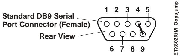
![Standard DB9 Serial\nPort Connector (Female)\nRear View\n1 2 3 4 5\n6 7 8 9\nETX802RfM_Oopsjump](.5001789aa-etx802refman/eda707841394a9dde4afac16c5deeaa64bb9afe4c3c3a0044d650e57097d6670.jpg)

Figure 3-1. Oops! Jumper Connection

# Serial Console (Remote Access)

The BIOS Setup Utility supports the serial console (or console redirection) feature, but refers to it as Remote Access. This I/O function can be accessed by an ANSI-compatible serial terminal, or the equivalent terminal emulation software running on another system. This can be very useful when setting up the BIOS on a production line for systems that are not connected to a keyboard and display (sometimes referred to as a headless system).

# Serial Console Setup

The serial console feature is implemented by connecting a standard null modem cable or a modified serial cable (or “Hot Cable”) between one of the serial ports, such as Serial 1 or Serial 2, and the serial terminal or a PC with communications software. The BIOS Setup Utility controls the serial console settings for the ETX 802. Refer to Accessing BIOS Setup Utility (Remote Access/Serial Console) and Advanced settings, in Chapter 4, BIOS Setup Utility for the Remote Access option to set the serial terminal, or PC with communications software.

# Hot (Serial) Cable

To convert a standard serial cable to a Hot Cable for use on the custom baseboard, two pins must be shorted together at the Serial port DB9 connector. Short together the RTS (7) and RI (9) pins on Serial port DB9 connector as shown in Figure 3-2.
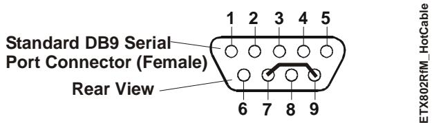
![Standard DB9 Serial\nPort Connector (Female)\nRear View\n1 2 3 4 5\n6 7 8 9\nETX802RM_HotCable](.5001789aa-etx802refman/2b77b4084fc8d3ae69a2d429ec323772e3fd1363b57ae92d2e31ef58db5abad4.jpg)

Figure 3-2. Hot Cable Jumper

# Temperature Monitoring

The temperature monitoring function is preformed by Analog Devices, ADM1023 chip and it takes an input connection from the thermal diode in the Intel Celeron M or Pentium M CPU. The ADM1023 chip uses the two-wire SMBus interface to communicate with the other devices on the SMBus, including the I/O Hub (82801DBM).

# NOTE

The ETX 802 requires a heatsink for all Intel CPUs and the Memory Hub (Northbridge), but no fan, below +70° C. The 1.4 GHz Pentium M requires a fan for extended temperatures (+70° to +85° C).

# Watchdog Timer (WDT)

The watchdog timer (WDT) restarts the system if an error or mishap occurs, allowing the system to recover from the mishap, even though the error condition may still exist. Possible problems include failure to boot properly, loss of control by the application software, failure of an interface device, unexpected conditions on the bus, or other hardware or software malfunctions.

The WDT (watchdog timer) can be used both during the boot process and during normal system operation.

• During the Boot process – If the operating system fails to boot in the time interval set in the BIOS, the system will reset.
The watchdog timer (WDT) is enabled and configured in the Boot settings screen of the BIOS Setup Utility. Set the WDT for a time-out interval in seconds, between 1 and 255, in one second increments. Ensure you allow enough time for the operating system to boot. The OS or application must tickle (reset) the WDT before the timer expires. This can be done by accessing the hardware directly or through a BIOS call.
During System Operation – An application can set up the WDT hardware through a BIOS call, or by accessing the hardware directly. Some Ampro Board Support Packages provide an API interface to the WDT. The application must tickle (reset) the WDT before the timer expires or the system will be reset. The BIOS implements interrupt 15 function 0C3h to manipulate the WDT.
Watchdog Code examples – Ampro will provide code examples on the ETX 802 Doc & SW CD-ROM illustrating how to control the WDT in the final release.

# Power Interface

The ETX 802 draws its input voltage (+5V) through the four connectors (X1, X2, X3, X4) on the custom baseboard, which requires an external power supply, typically an ATX power supply or other power source as the application requires. The ETX 802 generates its own internal voltages onboard, including the CPU core voltages and requires the externally supplied +5 volts DC +/- 5%.

The –5V, –12V, +12V and +3.3V voltages used for the PCI and ISA buses and the LVDS video connector are supplied to the baseboard and ETX 802 module from the externally connected power supply, typically an ATX power supply.

# Optional CPU Fan (P1)

Table 3-23 lists the pins and signals of the optional CPU Fan and it has 3 pins, single row, with 0.100" pin spacing.

Table 3-23. CPU Fan (P1)

<table><tr><td>Pin #</td><td>Signal</td><td>Description</td></tr><tr><td>1</td><td>GND</td><td>Ground</td></tr><tr><td>2</td><td>+5</td><td>+5.0 volts DC +/- 5%</td></tr><tr><td>3</td><td>Fan_Tach</td><td>Fan Speed Tachometer</td></tr></table>

Note: The shaded area denotes power or ground.

# Power and Sleep States

The following information only applies if an ATX power supply is connected to the ETX baseboard where the ETX 802 is installed. If a non-ATX power supply is used, then the ETX 802 is only controlled by the Power-On/Off switch on the power supply and the various sleep states are not available. The ACPI sleep states are OS dependent and not available if your OS does not support power management based on the ACPI standard. The signals used for control of the ATX power supply and sleep states in general is located in Table 3-20 and described in more detail under topics Power Control Signals and Power Management Signals earlier in this chapter.

# Power-On Switch

The Power-On switch, on or connected to the ETX Baseboard, turns the ETX 802 and its attached power supply to a fully On condition, if you are using an ATX power supply and an OS that supports sleep states. If the operating system (OS) supports sleep states, the OS will turn off the ETX 802 and its power supply during the OS shut down process. Typically, the Power-On switch will also transition the ETX 802, the ETX baseboard, and its power supply between a fully powered on state and the various sleep states, including a fully powered off state. If the OS does not support sleep states, then the Power-On switch only turns power, On or Off, to the ETX 802 and its baseboard.

Typically, an OS that supports ACPI, also allows the Power-On switch to be configured through a user interface. The Power-On switch for the ETX 802 must be provided on, or connected to the baseboard.

# Sleep States (ACPI)

The ETX 802 supports the ACPI (Advanced Configuration and Power Interface) standard, which is a key component of certain Operating Systems’ (OS’s) power management. The supported features (sleep states) listed here are only available when an ACPI-compliant OS is used for the ETX 802, such as Windows 2000/XP. The term “sleep” state refers to a low wake latency (reduced power consumption) state, which can be re-started (awakened) restoring full operation to the ETX 802.

In these various sleep states, the computer appears to be off, indicated by such things as no display on the attached monitor and no activity for the connected CD-ROM or hard drives. Normally, when a computer detects certain activity (i.e. power switch, mouse, keyboard, serial port, or certain types of LAN activity), it returns to a fully operational state.

# NOTE

Currently, the Power-On switch, Wake-on-Ring, Wake-on-LAN, Wake on RTX alarm, Wake on PME, and Keyboard/Mouse activity are the only activities that will wake the ETX 802 from a powered down state, such as Standby (S1), Suspend-to-RAM (S3), Hibernate (S4) and Power Off (S5). However, not all of the listed activities will wake each sleep state. Refer to the ETX 802 Software and Hardware Release Notes for more information.

The ETX 802 supports at least five ACPI power states, depending on the operating system used and its ability to manage sleep states. Typically, the Power-On switch is used to wake up from a sleep state, or transition from one state to another, but this is dependent on the operating system.

• 1st state is normal Power On (S0).

♦ To go to a fully powered on state, the ETX 802 must either be powered Off (S5), or in a sleep state (S1 or S4), and then the Power-On switch is pressed for less than 4 seconds (default).
♦ The ETX 802 can transition from this state (S0) to the various states described below, depending on the power management capability of the OS and how it is programmed.

• 2nd state is a standby state (S1).

In this state there are internal operations taking place, including the internal RTC (real time clock), contents of RAM, activity for the CPU, but the external peripherals, such as hard disk drives, CD-ROMs, and monitor are off. The ETX 802 appears to be on due to the Power-On LED.

♦ Normally, to enter this sleep state, the ETX 802 must be fully powered on (S0) and the OS transitions the ETX 802 into this standby state (S1) under user control.
To exit this sleep state a wake up event, such as the Power-On switch, is used to wake up the ETX 802 and restore full operation, including the Power-On LED. Typically, pressing the Power-On switch for less than 4 seconds (default) will restore full operation.

• 3rd state is a suspend-to-RAM state (S3).

This sleep state stores your open files and programs in RAM before powering down. In this state there are no internal operations taking place, except for the internal RTC (real time clock) and low power level keeping the contents of RAM alive. This includes no activity for the CPU and external peripherals, such as hard disk drives or CD-ROMs. The ETX 802's Power-On LED is off, but the S3 Mode LED is turned on only when in S3 Mode. This state is only safe as long as you have power to your system. If power is lost to the ATX power supply or the battery fails, then the contents of RAM is lost, including any open applications and data files. This state is quicker than S4, but much more volatile.

♦ Normally, to enter this sleep state, the ETX 802 must be fully powered on (S0) and the OS transitions the ETX 802 into this suspend-to-RAM (S3) state under user control.
To exit this sleep state a wake up event, such as the Power-On switch, is used to wake up the ETX 802 and restore full operation, including the Power-On LED, but the S3 Mode LED turns off. Typically, pressing the Power-On switch for less than 4 seconds (default) will restore full operation.

• 4th state is a hibernate or suspend-to-disk state (S4).

This condition stores the state of your system (open files and programs) on the hard disk drive before powering down. In this state there are no internal operations taking place, except for the internal RTC. This includes no activity for the RAM, CPU, and external peripherals, such as hard disk drives or CD-ROMs. The ETX 802 appears to be off, including the Power-On LED and the S3 Mode LED. Your system will take longer to wake-up in this sleep state than S3, but since your data is saved to the disk, it is more secure and should not be lost in the event of a power failure.

♦ To enter a hibernate or suspend-to-disk state, the ETX 802 must be fully powered on and the OS transitions the ETX 802 into this sleep state (S4) under user control.
To exit this sleep state a wake up even, such as the Power-On switch, is used to wake up the ETX 802 and restore full operation, including the Power-On LED. Typically, pressing the Power-On switch for less than 4 seconds (default) will restore full operation.

• 5th state is the normal power Off or shutdown (S5).

All activity stops except the internal clock, unless the power cord is removed from the power source.

♦ To go to a fully powered down state, the ETX 802 must either be powered On, or in a sleep state, and then the Power-On switch is pressed for more than 4-to-6 seconds.
♦ To go to a fully powered up state, press the Power-On switch for less than 4 seconds (default) and full operation is restored.

The OS may provide additional programming features to change the activation time for each state, and to shutdown or transition the ETX 802 at certain times, depending on the way the OS interface is programmed. Refer to the OS vender’s documentation for power management conditions under the ACPI standard.

# Introduction

This chapter describes the BIOS Setup Utility menus and the various screens used for configuring the ETX 802. Some features in the Operating System or application software may require configuration in the BIOS Setup Utility screens.

This section assumes the user is familiar with general BIOS Setup and does not attempt to describe the BIOS functions. Refer to the appropriate PC reference manuals for information about the onboard ROM-BIOS software interface. If Ampro has added to or modified the standard functions, these functions will be described.

The options provided for the ETX 802 are controlled by BIOS Setup. BIOS Setup is used to configure the board, modify the fields in the Setup screens, and save the results in the onboard configuration memory. Configuration memory consists of portions of the CMOS RAM in the battery-backed real-time clock chip and the flash memory.

The Setup information is retrieved from configuration memory when the board is powered up or when it is rebooted. Changes made to the Setup parameters, with the exception of the time and date settings, do not take effect until the board is rebooted.

Setup is located in the ROM BIOS and can be accessed while the board is in the Power-On Self Test (POST) state, just before starting the boot process. Typically, the screen displays a message indicating when you can press &lt;Del&gt; to enter the BIOS Setup Utility.

The ETX 802 BIOS Setup Utility is used to configure items in the BIOS using the following menus:

• Main • Security
• Advanced • Chipset
• PCIPnP • Power
• Boot • Exit

Table 4-1 summarizes the list of BIOS menus and some of the features available for ETX 802. The BIOS Setup menu offers the menu choices listed above and the related topics and screens are described on the following pages.

# Accessing BIOS Setup Utility (VGA Display)

To access the BIOS Setup Utility using a VGA display for the ETX 802:

1. Turn on the VGA monitor and the power supply to the ETX 802.
2. Start Setup by pressing the [Del] key, when the following message appears on the boot screen.

Hit &lt;Del&gt; if you want to run SETUP

# NOTE

If the setting for Quick Boot is set to [Enabled], you may not see this prompt appear on screen if the monitor is too slow to display it on start up. If this happens, press the &lt;Del&gt; key early in the boot sequence to enter the BIOS Setup Utility.

3. Use the &lt;Enter&gt; key to select the screen menus listed in the Opening BIOS screen. See Figure 4-1.
4. Follow the instructions at the bottom of each screen to navigate through the selections and modify any settings.

# Accessing BIOS Setup Utility (Remote Access)

Once you set up the BIOS Utility for Remote Access (serial console or console redirection) in VGA mode, entering the BIOS in the remote access mode, is very similar to the method used when entering the BIOS with a VGA display.

1. Turn on the power supply to the ETX 802 and baseboard to access the BIOS Setup Utility in VGA mode.
2. Set the BIOS feature Remote Access to [Enabled] under the Advanced menu.
3. Accept the default options or make your own selections for the balance of the Remote Access fields and record your settings.
4. Ensure you select the type of remote serial terminal you will be using and record your selection.
5. Select Save Changes and Exit and then shut down the ETX 802 and baseboard.
6. Connect the remote serial terminal (or the PC with communications software) to the COM port you selected on the ETX 802 using a Hot Cable or a standard null-modem serial cable.
7. Turn on the remote serial terminal (or the PC with communications software) and set it to the settings you selected and recorded earlier in the BIOS Setup Utility.
COM1, 115200, 8 bits, 1 stop bit, no parity, no flow control, and [Always] for Redirection After BIOS POST are the default settings for the ETX 802.
8. Restore power to the ETX 802 and look for the screen prompt shown below.

$\mathrm { \texttt { H i t } ~ { \hat { ~ } } C ~ \ i f ~ \mathrm { \texttt { Y o u } ~ w a n t ~ \ t o ~ \texttt { r u n } ~ S E T U P } }$

9. Press the CTRL–C keys to enter Setup early in the boot sequence, especially if Quick Boot is set to [Enabled].

If Quick Boot is set to [Enabled], you may never see the screen prompt.

10. Use the &lt;Enter&gt; key to select the screen menus listed in the Opening BIOS screen. See Figure 4-1.

<table><tr><td>NOTE</td><td>The serial console port is not hardware protected, and is not listed in the COM table within BIOS Setup Utility. Diagnostic software that probes hardware addresses may cause a loss or failure of the serial console functions.</td></tr></table>

Table 4-1. BIOS Setup Utility Menus

<table><tr><td>BIOS Setup Utility Menu</td><td>Item/Topic</td></tr><tr><td>Main Settings</td><td>Date and Time</td></tr><tr><td>Advanced Settings</td><td>CPU Configuration, IDE Configuration, Floppy Configuration, Super I/O Configuration, ACPI Configuration, MPS Configuration, Smbios Configuration, Remote Access (Serial Console) Configuration, and USB Configuration</td></tr><tr><td>PCIPnP (PCI, Plug n&#x27; Play)</td><td>PCI settings, Plug &amp; Play settings, Interrupt settings and DMA channel settings, Reserved memory</td></tr><tr><td>Boot</td><td>Boot up Settings Configuration, Boot Device Priority, Removable Drives</td></tr><tr><td>Security</td><td>Setting or changing Supervisor/User Passwords, Boot Sector Virus Protection</td></tr><tr><td>Chipset</td><td>Northbridge Configuration, Southbridge Configuration</td></tr><tr><td>Power</td><td>Power Management/APM and Resume Power conditions</td></tr><tr><td>Exit</td><td>Exiting with or without changing settings, Loading Optimal or Fail-safe conditions</td></tr></table>

# BIOS Setup Utility Menus

# Main Menu Screen

<table><tr><td colspan="8">BIOS Setup Utility</td></tr><tr><td>Main</td><td>Advanced</td><td>PCIPnP</td><td>Boot</td><td>Security</td><td>Chipset</td><td>Power</td><td>Exit</td></tr><tr><td colspan="5">System Overview</td><td rowspan="5" colspan="3">Use [ENTER], [TAB] or [SHIFT-TAB] to select a field.Use[+] or [-] to configure system time.</td></tr><tr><td colspan="5">AMIBIOS</td></tr><tr><td colspan="5">Version : 08.00.xxBuild Date: xx/xx/xxID : SWxxxxxxxx</td></tr><tr><td colspan="5">Processor</td></tr><tr><td colspan="5">Type : Intel(R) Pentium(R) M processor 1.40GHzSpeed : 1399MHzCount : 1</td></tr><tr><td colspan="5">System Memory</td><td colspan="3">Select Screen</td></tr><tr><td colspan="5">Size : 1016MB</td><td colspan="3">Select Item</td></tr><tr><td colspan="3">System Time</td><td colspan="2">[15:21:33]</td><td rowspan="2" colspan="3">+ - Change fieldTab Select FieldF1 General HelpF10 Save and ExitESC Exit</td></tr><tr><td colspan="3">System Date</td><td colspan="2">[Fri 08/25/2006]</td></tr></table>

V0x.xx (C) Copyright 1985-2004, American Megatrends, Inc.

Figure 4-1. Main Menu Screen

# System Overview

# • Date & Time

♦ System Time (hh:mm:ss) – This is a 24-hour clock setting in hours, minutes, and seconds
System Date (day of week, mm:dd:yyyy) – This field requires the alpha-numeric entry of the day of week, calendar month, day of the month, and all 4 digits of the year, indicating the century plus year (Fri 02/14/2006).

# NOTE

The Optimal Default values are shown highlighted as bold text and the Fail-safe Defaults are shown highlighted as italic text in the list of options. In many cases the Optimal values are the same as the Fail-safe values, so you will see text options as italic and bold text at the same time.

Refer to the right of the BIOS screens for navigation and selection instructions not listed in the following table.

Table 4-2. Exiting and Loading Default Keys

<table><tr><td>Key</td><td>Description</td></tr><tr><td>F7</td><td>Discard Changes without leaving BIOS Setup</td></tr><tr><td>F8</td><td>Load failsafe default settings.</td></tr><tr><td>F9</td><td>Load optimal default settings.</td></tr><tr><td>F10</td><td>Save Changes and Exit BIOS Setup</td></tr></table>

# Advanced Menu Screen

<table><tr><td colspan="8">BIOS Setup Utility</td></tr><tr><td>Main</td><td>Advanced</td><td>PCIPnP</td><td>Boot</td><td>Security</td><td>Chipset</td><td>Power</td><td>Exit</td></tr><tr><td colspan="5">Advanced Settings</td><td colspan="3">Configure CPU</td></tr><tr><td colspan="5">WARNING: Setting wrong values in below sections may cause system to malfunction.</td><td colspan="3"></td></tr><tr><td colspan="5">CPU ConfigurationIDE ConfigurationFloppy ConfigurationSuperIO ConfigurationACPI ConfigurationMPS ConfigurationSmbios ConfigurationRemote Access ConfigurationUSB Configuration</td><td></td><td colspan="2">Select ScreenSelect ItemEnter Go to Sub ScreenF1 General HelpF10 Save and ExitESC Exit</td></tr></table>

V0x.xx (C) Copyright 1985-2004, American Megatrends, Inc.

Figure 4-2. Advanced Menu Screen

Advanced Settings

>CPU Configuration

Configure advanced CPU settings

Module version - 11.05

Manufacture : Intel

Brand String : Intel® Pentium® M processor 1.40GHz

Frequency : 1.39GHz

FSB Speed : 400MHz

Cache L1 : 32kB

Cached L2 : 2048kB

• Intel® SpeedStep(™) Technology – [Maximum Speed], [Minimum Speed], [Automatic], or [Disabled]

This feature is only available for the Pentium CPU.

Intel® Mobile Pentium® Processors with Intel® SpeedStep™ technology lets you customize high performance computing on your mobile PC. When the ETX 802 is connected to the power, the ETX 802 COM will run applications with speed virtually identical to a desktop system. When powered by a battery, the processor drops to a lower frequency (by changing the bus ratios) and voltage, conserving battery life while maintaining a high level of performance. Manual override lets you boost the frequency back to the high frequency when on battery, allowing you to customize performance.

# >IDE Configuration

• OnBoard PCI IDE Controller – [Disabled], [Primary], [Secondary], or [Both]

This item specifies the IDE channels used by the onboard PCI IDE controller.

♦ If [Disabled] is selected, the ETX 802 is prevented from using either of the onboard IDE controllers.
♦ If [Primary] is selected, the BIOS only detects the Primary IDE channel, including both Primary Master and Primary Slave.
If [Secondary] is selected, the BIOS only detects the Secondary IDE channel, including both Secondary Master and Secondary Slave.
♦ If [Both] is selected, both Primary and Secondary IDE channels will be detected, including Master and Slave for each channel.

• OnBoard PCI IDE Operate Mode – [Legacy Mode] or [Native Mode]

Native mode is only used with Windows XP.

> Primary IDE Master – [Not Detected] or [Device Type]

∗ If the BIOS does not detect a device on the Primary IDE Master channel, [Not Detected] will be displayed. You can still go to the submenu to set options for an IDE device.

∗ If the BIOS auto detects a IDE device, the device type will be displayed; for example, [Hard Disk], with the parameters automatically selected, due to the default setting of Auto for Type.

• Type – [Not Installed], [Auto], [CD/DVD], or [ARMD]

This field sets the boot device type used by the BIOS after the Power On Self Test (POST) has completed.

∗ If [Not Installed] is selected, the BIOS is prevented from searching for an IDE disk drive on the specified channel.
∗ If [Auto] is selected, the BIOS auto any detects IDE disk drives on the specified channel. This is the default setting and should be used if an IDE hard disk drive is attached to the specified IDE channel.
∗ If [CD/DVD] is selected, the BIOS only searches for an IDE CD-ROM or IDE DVD device on the Primary IDE channel. The BIOS will not attempt to search for other types of IDE disk devices on the specified channel.
∗ If [ARMD] is selected, the BIOS detects an ATAPI Removable Media Device on the specified IDE channel. This includes, but is not limited to ZIP drives and LS-120 drives.

• LBA/Large Mode – [Disabled] or [Auto]

This field sets the LBA (Logical Block Addressing) on the IDE disk drive. In LBA mode with a setting of [Auto], the maximum drive capacity is greater than 137 GB.

• Block (Multi-Sector Transfer) – [Disabled] or [Auto]

This field sets the block mode multi-sector transfers option and allows the BIOS to auto detect device support for Multi-Sector Transfers on the specified channel. Block mode boosts IDE drive performance by increasing the amount of data transferred. Only 512 bytes of data can be transferred per interrupt if block mode is not used. Block mode allows transfers of up to 64 kB per interrupt.

∗ If [Auto] is selected, the BIOS will auto detect the number of sectors per block for transfer from the hard disk drive to the memory. The data transfer to and from the device will occur multiple sectors at a time.

• PIO Mode – [Auto], [0], [1], [2], [3], or [4]

This field sets the IDE PIO (Programmable I/O) mode and programs the timing cycles between the IDE drive and the programmable IDE controller. As the PIO mode increases, the cycle time decreases.

∗ If [Auto] is selected, the BIOS auto detects the PIO mode.
∗ If [0] is selected, the BIOS uses PIO mode 0, with a data transfer rate of 3.3 MBs.
∗ If [1] is selected, the BIOS uses PIO mode 1, with a data transfer rate of 5.2 MBs.
∗ If [2] is selected, the BIOS uses PIO mode 2, with a data transfer rate of 8.3 MBs.
∗ If [3] is selected, the BIOS uses PIO mode 3, with a data transfer rate of 11.1 MBs.
∗ If [4] is selected, the BIOS uses PIO mode 4, with a data transfer rate of 16.6 MBs.

DMA Mode – [Auto], [SWDMA0], [SWDMA01], [SWDMA2], [MWDMA0], [MWDMA1], [MWDMA2], [UDMA0], [UDMA1], [UDMA2], [UDMA3], [UDMA4], [UDMA5], or [UDMA6]

This field allows you to select DMA modes and adjust the respective transfer rate. The list of available DMA modes is dependent on the IDE device and its supported modes, including the transfer speed and cable type (40-pin or 80-pin).

$$
\text { SWDMAn } = \text { Single   Word   DMA   mode   n }
$$

$$
\text { MWDMAn } = \text { Multi   Word   DMA   mode   n }
$$

$$
\mathrm{UDMAn} = \text { Ultra   DMA   mode   n }
$$

∗ If [Auto] is selected, the BIOS auto detects the DMA Mode. Use this value if the IDE disk drive support cannot be determined.
∗ If [SWDMA0] is selected, the BIOS uses Single Word DMA mode 0, with a data transfer rate of 2.1 MBs.
∗ If [SWDMA1] is selected, the BIOS uses Single Word DMA mode 1, with a data transfer rate of 4.2 MBs.
∗ If [SWDMA2] is selected, the BIOS uses Single Word DMA mode 2, with a data transfer rate of 8.3 MBs.
∗ If [MWDMA0] is selected, the BIOS uses Double Word DMA mode 0, with a data transfer rate of 4.2 MBs.
∗ If [MWDMA1] is selected, the BIOS uses Double Word DMA mode 1, with a data transfer rate of 13.3 MBs.
∗ If [MWDMA2] is selected, the BIOS uses Double Word DMA mode 2, with a data transfer rate of 16.6 MBs.
∗ If [UDMA0] is selected, the BIOS uses Ultra DMA mode 0, with a data transfer rate of 16.6 MBs.
∗ If [UDMA1] is selected, the BIOS uses Ultra DMA mode 1, with a data transfer rate of 25 MBs.
∗ If [UDMA2] is selected, the BIOS uses Ultra DMA mode 2, with a data transfer rate of 33.3 MBs.

# NOTE

The following DMA modes, UDMA3, UDMA4, UDMA5, or UDMA6, require an 80-conductor ATA cable and may not appear without it.

∗ If [UDMA3] is selected, the BIOS uses Ultra DMA mode 3, with a data transfer rate of 44.4 MBs. To use this mode, an 80-conductor ATA cable is required.

∗ If [UDMA4] is selected, the BIOS uses Ultra DMA mode 4, with a data transfer rate of 66.6 MBs. To use this mode, an 80-conductor ATA cable is required.
∗ If [UDMA5] is selected, the BIOS uses Ultra DMA mode 5, with a data transfer rate of 99.9 MBs. To use this mode, an 80-conductor ATA cable is required.
∗ If [UDMA6] is selected, the BIOS uses Ultra DMA mode 6, with a data transfer rate of 133.2 MBs. To use this mode, an 80-conductor ATA cable is required.

• S.M.A.R.T.– [Auto], [Disabled], or [Enabled]

The Self-Monitoring Analysis and Reporting Technology (SMART) feature can help predict impending drive failures.

∗ If [Auto] is selected, the BIOS auto detects hard disk drive support. Use this setting if the IDE disk drive support cannot be determined.
∗ If [Disabled] is selected, the BIOS is prevented from using SMART feature.
∗ If [Enabled] is selected, the BIOS uses the SMART feature on the hard disk drives.

• 32Bit Data Transfer – [Disabled] or [Enabled]

This field sets the 32-bit data transfer rate.

If [Enabled] is selected, the BIOS uses 32-bit data transfers on the supported hard disk drive.

# > Primary IDE Slave – [Not Detected] or [Device Type]

The descriptions used for the Primary IDE Master are the same for the Primary IDE Slave except where noted.

• Type – [Not Installed], [Auto], [CD/DVD], or [ARMD]
∗ If [Not Installed] appears due to Not Detected, the balance of the options for Primary IDE Slave do not appear on screen.
• LBA/Large Mode – [Disabled] or [Auto]
• Block (Multi-Sector Transfer) – [Disabled] or [Auto]
• PIO Mode – [Auto], [0], [1], [2], [3], or [4]
DMA Mode – [Auto], [SWDMA0], [SWDMA01], [SWDMA2], [MWDMA0], [MWDMA1], [MWDMA2], [UDMA0], [UDMA1], [UDMA2], [UDMA3], [UDMA4], [UDMA5], or [UDMA6]
• S.M.A.R.T.– [Auto], [Disabled], or [Enabled]
• 32Bit Data Transfer – [Disabled] or [Enabled]

# > Secondary IDE Master – [Not Detected] or [Device Type]

The descriptions used for the Primary IDE Master are the same for the Secondary IDE Master except where noted.

• Type – [Not Installed], [Auto], [CD/DVD], or [ARMD]
∗ If [Not Installed] appears due to Not Detected, the balance of the options for Secondary IDE Master do not appear on screen.
• LBA/Large Mode – [Disabled] or [Auto]
• Block (Multi-Sector Transfer) – [Disabled] or [Auto]
• PIO Mode – [Auto], [0], [1], [2], [3], or [4]
DMA Mode – [Auto], [SWDMA0], [SWDMA01], [SWDMA2], [MWDMA0], [MWDMA1], [MWDMA2], [UDMA0], [UDMA1], [UDMA2], [UDMA3], [UDMA4], [UDMA5], or [UDMA6]
• S.M.A.R.T.– [Auto], [Disabled], or [Enabled]

• 32Bit Data Transfer – [Disabled] or [Enabled]

> Secondary IDE Slave – [Not Detected] or [Device Type]

The descriptions used for the Primary IDE Master are the same for the Secondary IDE Slave except where noted.

• Type – [Not Installed], [Auto], [CD/DVD], or [ARMD]
∗ If [Not Installed] appears due to Not Detected, the balance of the options for Secondary IDE Slave do not appear on screen.
• LBA/Large Mode – [Disabled] or [Auto]
• Block (Multi-Sector Transfer) – [Disabled] or [Auto]
• PIO Mode – [Auto], [0], [1], [2], [3], or [4]
DMA Mode – [Auto], [SWDMA0], [SWDMA01], [SWDMA2], [MWDMA0], [MWDMA1], [MWDMA2], [UDMA0], [UDMA1], [UDMA2], [UDMA3], [UDMA4], [UDMA5], or [UDMA6]
• S.M.A.R.T. for hard disk drives – [Auto], [Disabled], or [Enabled]
• 32Bit Data Transfer – [Disabled] or [Enabled]

• Hard disk drive Write Protect – [Disabled] or [Enabled]

This field protects the hard disk drive from being overwritten.

∗ If [Disabled] is selected, the HDD operates normally, allowing Read, Write, and Erase functions to be performed on the IDE hard disk drive.
∗ If [Enabled] is selected, the BIOS is prevents the IDE HDD from being erased.

• IDE Detect Time Out (Seconds) – [0], [5], [10], [15], [20], [25], [30], or [35]

The field determines how long the BIOS searches for the available IDE devices on the specified channels. Some IDE HDDs take the BIOS longer to locate than others, but this field allows you fine-tune the settings to allow for faster boot times.

∗ If [0] is selected, the BIOS does not search for an IDE device. This is the best setting to use if the onboard IDE controllers are set to a specific IDE HDD in the BIOS.
∗ If [5] is selected, the BIOS stops searching for an IDE device after 5 seconds. A large majority of ultra ATA HDDs can be detected with within 5 seconds.
∗ If [10] is selected, the BIOS stops searching for an IDE device after 10 seconds.
∗ If [15] is selected, the BIOS stops searching for an IDE device after 15 seconds.
∗ If [20] is selected, the BIOS stops searching for an IDE device after 20 seconds.
∗ If [25] is selected, the BIOS stops searching for an IDE device after 25 seconds.
∗ If [30] is selected, the BIOS stops searching for an IDE device after 30 seconds.
∗ If [35] is selected, the BIOS stops searching for an IDE device after 35 seconds. This is the default setting and is the recommended setting when all IDE connectors are set to Auto.

• ATA (PI) 80 pin Cable Detection – [Host & Device], [Host], or [Device]

This field selects the method used to detect the ATA (PI) 80-pin cable. The default setting for EXT 802 BIOS is 40-pins.

∗ If [Host & Device] is selected, the BIOS uses both the onboard IDE controller and the IDE hard disk drive (HDD) to detect the type of IDE cable used.
∗ If [Host] is selected, the BIOS uses only the onboard IDE controller to detect the type of IDE cable used.

∗ If [Device] is selected, the BIOS uses only the IDE hard disk drive (HDD) to detect the type of IDE cable used.

# NOTE

An 80-conductor ATA cable is required when operating with Ultra ATA/66, Ultra ATA/100 and Ultra ATA/133 IDE hard disk drives. The standard 40-conductor ATA cable cannot handle the higher speeds. Due to the plug compatibility of the 80-conductor ATA cable to the standard 40-conductor ATA cable, the BIOS must have a feature to set this or determine if the 80-conductor ATA cable is present. The BIOS detects a break in one of the lines on the 80-conductor ATA cable that is normally an unbroken connection in the standard 40-conductor ATA cable. If a faster speed is set in the BIOS than the connected cable can support, the BIOS instructs the IDE HDD to run at the correct speed for the cable type detected.

# >Floppy Configuration

• Drive A – [Disabled], [360 kB, 5 1/4 "], [1.2 MB, 1/4"], [720 kB, 3 1/2"], [1.44 MB, 3 1/2"], or [2.88 MB, 3.5"]
• Drive B – [Disabled], [360 kB, 5 1/4"], [1.2 MB, 1/4"], [720 kB, 3 1/2"], [1.44 MB, 3 1/2"], or [2.88 MB, 3.5"]

# >Super I/O Configuration

• Onboard Floppy Controller – [Disabled] or [Enabled]

∗ If this feature is [Enabled], the onboard floppy controller is selected over the Parallel Port and the entry, 1st Floppy Drive, appears in the boot order under Boot Device Priority. You must select a Floppy A, typically [1.44 MB, 3 1/2"] to use this feature. The Parallel Port can not be enabled since these two devices share the same pins on the baseboard interface connector.
∗ If this feature is [Disabled], the Parallel Port can be Enabled by selecting one of the Parallel port address.

• Serial Port 1 Address – [Disabled], [3F8/IRQ4], [2F8/IRQ3], [3E8/IRQ4], or [2E8/IRQ3]
• Serial Port 2 Address – [Disabled], [3F8/IRQ4], [2F8/IRQ3], [3E8/IRQ4], or [2E8/IRQ3]

♦ Serial Port 2 Mode – [Normal], [IrDA], or [ASK IR]

∗ If [IrDA] or [ASK IR] are selected, the following items appear on screen.

◊ IR Duplex mode – [Half Duplex] or [Full Duplex]
◊ IR I/O Pin select – [SINB/SOUTB] or [IRRX/IRTX]
◊ COMB Receiver Polarity – [High] or [Low]
◊ COMB Xmitter Polarity – [High] or [Low]

• Parallel Port Address – [Disabled], [378], [278], or [3BC]

If [378], [278], or [3BC] are selected, the following items appear on screen.

♦ Parallel Port Mode– [Normal], [Bi-Directional], [EPP], or [ECP]

∗ If [Normal] is selected, the standard parallel port mode is used. This is the default setting.
∗ If [Bi-Directional] is selected, the data is sent to and received from the parallel port.
∗ If [EPP] is selected, the following options are listed. The parallel port can be used with devices adhering to the Enhanced Parallel Port (EPP) specification. EPP uses the existing parallel port signals to provide asymmetric bi-directional data transfer driven by the host device.

◊ EPP version [1.9] or [1.7]

∗ If [ECP] is selected, the following options are listed. The parallel port can be used with devices adhering to the Extended Capabilities Port (ECP) specification. ECP uses the DMA protocol to achieve data transfer rates up to 2.5 Megabits per second. ECP also provides symmetric bi-directional communication.

◊ ECP Mode DMA Channel [DMA3], [DMA0], or [DMA1]

♦ Parallel Port IRQ – [IRQ5] or [IRQ 7]

# >ACPI Configuration

• General ACPI Configuration

♦ Suspend Mode – [Auto], [S1 (POS)], or [S3 (STR)]

This field determines which sleep state (S1 or S3) is used for suspended mode.

∗ If [Auto] or [S3 (STR)] is selected, the following item appears on screen. Enabling S3 will also enable the S3 Mode LED on the ETX 802.

• Repost Video on S3 Resume – [No] or [Yes]

∗ If [Yes] is selected, the video BIOS is initialized coming out of the S3 state. Some video controllers require this option to be enabled.

∗ If [No] is selected, the video BIOS will not be initialized coming out of the S3 state.

• Advanced ACPI Configuration

♦ ACPI 2.0 Features – [No] or [Yes]

If [Yes] is selected, the BIOS will support the ACPI 2.0 specifications.

♦ Headless Mode – [Disabled] or [Enabled]

If [Enabled] is selected, the ACPI FACP (Fixed System Description Table) table is updated to indicate headless operation mode through ACPI. Today, headless operation implies no keyboard or mouse.

• Chipset ACPI Configuration

♦ APIC ACPI SCI IRQ – [Disabled] or [Enabled]

♦ USB Device Wakeup from S3 – [Disabled] or [Enabled]

# >MPS Configuration

• MPS Configuration Version – [1.1] or [1.4]

# >Smbios Configuration

• Smbios Smi Support – [Disabled] or [Enabled]

# >Remote Access Configuration

• Remote Access – [Hotcable] or [Enabled]

This field enables the remote access (Serial Console or Console Redirection) features.

Serial Port Number – [COM1] or [COM2]

Base Address, IRQ [2F8h, 3]

♦ Serial Port Mode – [115200, 8, n, 1], [57600, 8, n, 1], [38400, 8, n, 1], [19200, 8, n, 1], or [09600, 8, n, 1]

If [57600, 8, n, 1] is selected, the remote Serial Terminal should be set for 57.6 kHz baud rate with 8 start bits, no parity, and 1 stop bit.

♦ Flow Control – [None], [Hardware], or [Software]
∗ If [Hardware] is selected, flow control is handled by hardware.
∗ If [Software] is selected, flow control is handled by software.
♦ Redirection After BIOS Post – [Disabled], [Boot Loader], or [Always]
♦ Terminal Type – [ANSI], [VT100], or [VT-UTF8]
∗ If [VT-UTF8] is selected, the following item disappear from the screen.
• VT-UTF8 Combo Key Support – [Disabled] or [Enabled]
♦ Sredir Memory Display Delay – [No Delay], [Delay 1 sec], [Delay 2 sec] or [Delay 4 sec]

# >USB Configuration

Depending on the USB devices detected, examples similar to those listed below may be displayed.

Module Version - x.xx.xx-xx.x

Or

Module Version - x.xx.xx-xx.x

USB Devices Enabled: 2 drives

USB Devices Enabled: None:

• USB Function – [Disabled], [2 USB ports], or [4 USB ports]

∗ If [Disabled] is selected, remaining options for USB, except USB 2.0 Controller, will disappear from the screen.

• Legacy USB Support – [Disabled], [Enabled], or [Auto]

This field supports the USB mouse and USB keyboard when no USB drivers are loaded for the operating system (OS).

∗ If [Disabled] is selected, remaining options for USB, except USB 2.0 Controller, will disappear from the screen.

∗ If [Enabled] is not enabled, the attached USB mouse and USB keyboard will not be available until a USB compatible OS is fully booted with all the USB drivers loaded.

∗ If [Auto] is selected, Legacy USB Support is disabled if no USB devices are connected.

NOTE

If this field is not enabled with [Enabled] or [Auto] the USB mouse and USB keyboard will not be recognized by the BIOS until the OS is fully booted and the USB drivers are loaded.

∗ If [Enabled] is selected, USB devices may be used during boot time and while using DOS.

∗ If [Auto] is selected, USB devices like, a USB keyboard or USB mouse will be automatically detected and if found, will be initialized and utilized during Boot time.

• USB 2.0 Controller – [Disabled] or [Enabled]

∗ If [Disabled] is selected, the following item disappears from the screen.

♦ USB 2.0 Controller Mode – [Full Speed] or [Hi Speed]

This field configures the USB 2.0 controller for [Full Speed = 12 Mbps] or [Hi Speed = 480 Mbps]

• BIOS EHCI Hand-Off – [Disabled] or [Enabled]

This field is used as work around for operating systems (OSs) that do not have EHCI hand-off support. The EHCI ownership change should be claimed by the EHCI driver.

# >USB MASS Storage Device Configuration

• USB Mass Storage Reset Delay – [10 sec], [20 sec], [30 sec], or [40 sec]

This field determines the number of seconds POST waits for the storage device after the start unit command is sent.

♦ Device #1 – [Mfg + model or device type]
♦ Emulation Type – [Auto], [Floppy], [Forced FDD], [Hard Disk], or [CDROM]

This field emulates USB device types.

∗ If this field is set to [Auto] it will emulate USB devices less than 530 MB as Floppy and devices larger than 530 MB as Hard Drives.
∗ If the [Forced FDD] options is selected, a HDD formatted drive can be forced to boot as FDD (except ZIP drives).

The remaining fields only appear if the BIOS detects additional USB mass storage devices up to three more USB devices.

♦ Device #2 – [Mfg + model or USB device type]
♦ Emulation Type – [Auto], [Floppy], [Forced FDD], [Hard Disk], or [CDROM]
♦ Device #3 – [Mfg + model or USB device type]
♦ Emulation Type – [Auto], [Floppy], [Forced FDD], [Hard Disk], or [CDROM]
♦ Device #4 – [Mfg + model or USB device type]
♦ Emulation Type – [Auto], [Floppy], [Forced FDD], [Hard Disk], or [CDROM]

PCIPnP (Plug & Play) Menu Screen

<table><tr><td colspan="8">BIOS Setup Utility</td></tr><tr><td>Main</td><td>Advanced</td><td>PCIPnP</td><td>Boot</td><td>Security</td><td>Chipset</td><td>Power</td><td>Exit</td></tr><tr><td colspan="5">Advance PCI/PnP Settings</td><td rowspan="2" colspan="3">Clear NVRAM during system boot.</td></tr><tr><td colspan="5">WARNING: Setting wrong values in below sections may cause system to malfunction.</td></tr><tr><td>Clear NVRAM</td><td>[No]</td><td></td><td></td><td></td><td></td><td></td><td></td></tr><tr><td>Plug &amp; Play O/S</td><td>[Yes]</td><td></td><td></td><td></td><td></td><td></td><td></td></tr><tr><td>PCI Latency timer</td><td>[64]</td><td></td><td></td><td></td><td></td><td></td><td></td></tr><tr><td>Allocate IRQ to PCI VGA</td><td>[Yes]</td><td></td><td></td><td></td><td></td><td></td><td></td></tr><tr><td>Pallette Snooping</td><td>[Disabled]</td><td></td><td></td><td></td><td></td><td></td><td></td></tr><tr><td>PCI IDE BusMaster</td><td>[Enabled]</td><td></td><td></td><td></td><td></td><td></td><td></td></tr><tr><td>OffBoard PCI/ISA IDE Card</td><td>[Auto]</td><td></td><td></td><td></td><td></td><td></td><td></td></tr><tr><td>IRQ3</td><td>[Available]</td><td></td><td></td><td></td><td></td><td>Select Screen</td><td></td></tr><tr><td>IRQ4</td><td>[Available]</td><td></td><td></td><td></td><td></td><td>Select Item</td><td></td></tr><tr><td>IRQ5</td><td>[Available]</td><td></td><td></td><td></td><td>+ -</td><td>Change field</td><td></td></tr><tr><td>IRQ7</td><td>[Available]</td><td></td><td></td><td></td><td>F1</td><td>General Help</td><td></td></tr><tr><td>IRQ9</td><td>[Available]</td><td></td><td></td><td></td><td>F10</td><td>Save and Exit</td><td></td></tr><tr><td>IRQ10</td><td>[Available]</td><td></td><td></td><td></td><td>ESC</td><td>Exit</td><td></td></tr><tr><td>IRQ11</td><td>[Available]</td><td></td><td></td><td></td><td></td><td></td><td></td></tr></table>

V0x.xx (C) Copyright 1985-2004, American Megatrends, Inc.

Figure 4-3. PCIPnP Menu Screen

# Advance PCI/PnP Settings

• Clear NVRAM – [No] or [Yes]

This field is used to clear NVRAM during system boot.

• Plug & Play O/S – [No] or [Yes]

∗ If [No] is selected, the BIOS is allowed to configure all the devices in the system.
∗ If [Yes] is selected, the Operating System (OS) is allowed to configure Plug and Play (PnP) devices not required for boot if your ETX 802 is using a Plug and Play OS. The OS is allowed to change the interrupt, I/O, and DMA settings for the devices in the system.

• PCI Latency timer – [32], [64], [96], [128], [160], [192], [224], or [248]

This feature sets the latency of all PCI devices on the PCI bus. The various settings allow the PCI Latency timer to be adjusted to the number of clock cycles specified. The default setting [64] adjust the PCI Latency timer to 64 PCI clock cycles.

• Allocate IRQ to PCI VGA – [Yes] or [No]

This field allows or restricts the system from giving the VGA adapter card an interrupt address.

∗ If [Yes] is selected, the BIOS is allowed to allocate an IRQ to any VGA adapter card that uses the PCI local bus.

• Palette Snooping – [Disabled] or [Enabled]

∗ If [Disabled] is selected, the BIOS prevents an installed VGA card from using Palette Snooping, even if the VGA card request IRQs. This should not be changed unless the VGA card manufacturer requires this feature to be Enabled.

∗ If [Enabled] is selected, PCI devices are informed an ISA graphics card is installed in the system so the card will function correctly.

• PCI IDE BusMaster – [Disabled] or [Enabled]

∗ If [Enabled] is selected, the BIOS allows the IDE controller on the PCI local bus to have bus mastering capabilities, including reading/writing to IDE drives.

• OffBoard PCI/ISA IDE card – [Auto], [PCI Slot 1], [PCI Slot 2], [PCI Slot 3], or [PCI Slot 4]

∗ If [Auto] is selected, which works with most PCI IDE cards, it allows BIOS to automatically select the location of an OffBoard PCI IDE adapter card. Don't select the other PCI slot positions, unless the IDE adapter card is installed in the respective card slot position.

∗ If [PCI Slot 1] to [PCI Slot 4] are selected the following options appear:

• OffBoard PCI IDE Primary IRQ – [Disabled], [INTA], [INTB], [INTC], [INTD], or [Hardwired]

∗ If [Disabled] is selected, the PCI Slot # does not use or need an IRQ.

∗ If [INT#] is selected, the PCI Slot # needs an IRQ assigned to the device installed in the PCI slot.

• OffBoard PCI IDE Secondary IRQ – [Disabled], [INTA], [INTB], [INTC], [INTD], or [Hardwired]

∗ If [Disabled] is selected, the PCI Slot # does not use or need an IRQ.

∗ If [INT#] is selected, the PCI Slot # needs an IRQ assigned to the device installed in the PCI slot.

• IRQ3 – [Available] or [Reserved]

∗ If [Available] is selected, the BIOS can assign this IRQ to a PCI/PnP device.

∗ If [Reserved] is selected, the BIOS holds this IRQ for a legacy ISA device.

• IRQ4 – [Available] or [Reserved]

∗ If [Available] is selected, the BIOS can assign this IRQ to a PCI/PnP device.

∗ If [Reserved] is selected, the BIOS holds this IRQ for a legacy ISA device.

• IRQ5 – [Available] or [Reserved]

∗ If [Available] is selected, the BIOS can assign this IRQ to a PCI/PnP device.

∗ If [Reserved] is selected, the BIOS holds this IRQ for a legacy ISA device.

• IRQ7 – [Available] or [Reserved]

∗ If [Available] is selected, the BIOS can assign this IRQ to a PCI/PnP device.

∗ If [Reserved] is selected, the BIOS holds this IRQ for a legacy ISA device.

• IRQ9 – [Available] or [Reserved]

∗ If [Available] is selected, the BIOS can assign this IRQ to a PCI/PnP device.

∗ If [Reserved] is selected, the BIOS holds this IRQ for a legacy ISA device.

• IRQ10 – [Available] or [Reserved]

∗ If [Available] is selected, the BIOS can assign this IRQ to a PCI/PnP device.

∗ If [Reserved] is selected, the BIOS holds this IRQ for a legacy ISA device.

• IRQ11 – [Available] or [Reserved]

∗ If [Available] is selected, the BIOS can assign this IRQ to a PCI/PnP device.

∗ If [Reserved] is selected, the BIOS holds this IRQ for a legacy ISA device.

• IRQ14 – [Available] or [Reserved]
∗ If [Available] is selected, the BIOS can assign this IRQ to a PCI/PnP device.
∗ If [Reserved] is selected, the BIOS holds this IRQ for a legacy ISA device.
• IRQ15 – [Available] or [Reserved]
∗ If [Available] is selected, the BIOS can assign this IRQ to a PCI/PnP device.
∗ If [Reserved] is selected, the BIOS holds this IRQ for a legacy ISA device.
• DMA Channel 0 – [Available] or [Reserved]
∗ If [Available] is selected, the BIOS can assign this DMA Channel to a PCI/PnP device.
∗ If [Reserved] is selected, the BIOS holds this DMA Channel for a legacy ISA device.
• DMA Channel 1 – [Available] or [Reserved]
∗ If [Available] is selected, the BIOS can assign this DMA Channel to a PCI/PnP device.
∗ If [Reserved] is selected, the BIOS holds this DMA Channel for a legacy ISA device.
• DMA Channel 3 – [Available] or [Reserved]
∗ If [Available] is selected, the BIOS can assign this DMA Channel to a PCI/PnP device.
∗ If [Reserved] is selected, the BIOS holds this DMA Channel for a legacy ISA device.
• DMA Channel 5 – [Available] or [Reserved]
∗ If [Available] is selected, the BIOS can assign this DMA Channel to a PCI/PnP device.
∗ If [Reserved] is selected, the BIOS holds this DMA Channel for a legacy ISA device.
• DMA Channel 6 – [Available] or [Reserved]
∗ If [Available] is selected, the BIOS can assign this DMA Channel to a PCI/PnP device.
∗ If [Reserved] is selected, the BIOS holds this DMA Channel for a legacy ISA device.
• DMA Channel 7 – [Available] or [Reserved]
∗ If [Available] is selected, the BIOS can assign this DMA Channel to a PCI/PnP device.
∗ If [Reserved] is selected, the BIOS holds this DMA Channel for a legacy ISA device.
• Reserved Memory – [Disabled], [16k], [32k], or [64k]
This field reserves the memory block size for Legacy ISA devices.
∗ If [Disabled] is selected, the BIOS is prevented from reserving memory for ISA devices.
∗ If [64k] is selected, the BIOS reserves 64k of system memory for ISA devices at the Reserved Memory Address of [C8000].
• PCI Slot 1 – IRQ Preference– [Auto]. [3], [4], [5], [7], [9], [10], [11], [12], [14], or [15]
These fields select the PCI slot IRQ preference. Manually selecting IRQs does not guarantee the PCI slot devices will be configured with the IRQ choices, because PnP ISA cards (if present) are assigned the available resources before PCI devices.
• PCI Slot 2 – IRQ Preference– [Auto]. [3], [4], [5], [7], [9], [10], [11], [12], [14], or [15]
• PCI Slot 3 – IRQ Preference– [Auto]. [3], [4], [5], [7], [9], [10], [11], [12], [14], or [15]
• PCI Slot 4 – IRQ Preference– [Auto]. [3], [4], [5], [7], [9], [10], [11], [12], [14], or [15]

# Boot Menu Screen

<table><tr><td colspan="8">BIOS Setup Utility</td></tr><tr><td>Main</td><td>Advanced</td><td>PCIPnP</td><td>Boot</td><td>Security</td><td>Chipset</td><td>Power</td><td>Exit</td></tr><tr><td colspan="5">Boot Settings</td><td rowspan="3" colspan="3">Configure Settings during System Boot</td></tr><tr><td colspan="5">►Boot Settings Configuration</td></tr><tr><td colspan="5">►Boot Device Priority
►Hard Disk Drives
►Removable Drives
►CD/DVD Drives</td></tr><tr><td></td><td></td><td></td><td></td><td></td><td></td><td colspan="2">Select Screen
Select Item</td></tr><tr><td></td><td></td><td></td><td></td><td></td><td>Enter</td><td colspan="2">Go to Sub screen</td></tr><tr><td></td><td></td><td></td><td></td><td></td><td>F1</td><td colspan="2">General Help</td></tr><tr><td></td><td></td><td></td><td></td><td></td><td>F10</td><td colspan="2">Save and Exit</td></tr><tr><td></td><td></td><td></td><td></td><td></td><td>ESC</td><td colspan="2">Exit</td></tr></table>

V0x.xx (C) Copyright 1985-2004, American Megatrends, Inc.

Figure 4-4. Boot Menu Screen

# Boot Settings

# >Boot Settings Configuration

• Quick Boot – [Disabled] or [Enabled]

∗ If [Disabled] is selected, the BIOS is allowed to perform all POST test, but this slows the boot process.
∗ If [Enabled] is selected, the BIOS is allowed to skip certain POST tests to boot faster.

• Quiet Boot – [Disabled] or [Enabled]

∗ If [Disabled] is selected, the BIOS is allowed to display the POST messages on screen.
∗ If [Enabled] is selected, the BIOS displays the customized splash screen (OEM boot logo). The splash screen image (or boot logo) will appear on the display instead of the POST messages.

For more information about how to customized a splash screen image(OEM boot logo), refer to the Splash Screen files in the CD-ROM/Software/Misc/Splash directory on the ETX 802 Doc & SW CD-ROM for instructions when creating your own logo to display.

• AddOn ROM Display Mode – [Force BIOS] or [Keep Current]

∗ If [Force BIOS] is selected, any third party BIOS or add-on ROM messages will be displayed on screen during the boot process.
∗ If [Keep Current] is selected, no third party BIOS messages will be displayed on screen during the boot process.

• Bootup Num-Lock – [Off] or [On]

This field enables or disables the Num-Lock (Number Lock) keypad, including the 10-key numeric keys, to be turned on or off automatically when the system boots up. The field selection will remain unchanged until the Num-Lock key on the keyboard is pressed to change the Num-Lock state.

• PS/2 Mouse Support – [Disabled], [Enabled], or [Auto]

∗ If [Disabled] is selected, the PS/2 Mouse will not have access to system resources and will not be active after boot up.
∗ If [Enabled] is selected, the PS/2 Mouse can be used and will have access to system resources after boot up.
∗ If [Auto] is selected, the BIOS will detect the PS/2 Mouse automatically, if present, during the boot process. The PS/2 Mouse will have access to system resources and be active after boot up.

• Wait for 'F1' If Error – [Disabled] or [Enabled]

∗ If [Disabled] is selected, this does not allow for user intervention if an error occurs. Use this setting only when a known BIOS error will appear.
∗ If [Enabled] is selected, allows the BIOS to display an Error message indicating when an error has occurred during POST (power on self test) and wait for you to respond by hitting the &lt;F1&gt; key. Pressing &lt;F1&gt; will enter Setup and the BIOS setting can be adjusted to fix the problem.

• Hit 'Del' Message Display – [Disabled] or [Enabled]

∗ If [Disabled] is selected, the BIOS will not place the “Hit Del to enter Setup" message on screen during the boot process. If Quiet Boot is enabled, the Hit 'Del" message will not display.
∗ If [Enabled] is selected, the BIOS will place the “Hit Del to enter Setup" message on screen during the boot process, to indicate when you may press “Del” to enter the BIOS Setup menus.

• Interrupt 19 Capture – [Disabled] or [Enabled]

∗ If [Disabled] is selected, the BIOS prevents option ROMs from trapping interrupt 19.
∗ If [Enabled] is selected, the BIOS allows option ROMs to trap interrupt 19.

• Watchdog Timeout in Seconds – [Disabled] or [1-255]

\* If this field [1-255] is enabled by selecting a time interval (select a whole number between 255 seconds and 1 second), it will direct the watchdog timer to reset the system if it fails to boot the OS properly. Refer to the watchdog timer section in Chapter 3 for more information.

# >Boot Device Priority

Use these fields to set the boot device priority (boot order), which determines the boot sequence used by the BIOS to check for a boot device. You set the boot order by selecting from the list of the available boot devices, as well as, changing the order of the device types. Refer to the following examples, including the device types.

• 1st Boot Device – [Disabled], [1st Floppy Drive], [Hard Drive], [CD/DVD], or [Network: IBA FE Slot 01xx]

∗ Example, [1st Floppy Drive]

2nd Boot Device – [Disabled], [1st Floppy Drive], [Hard Drive], [CD/DVD], or [Network: IBA FE Slot 01xx]

∗ Example, [CD/DVD: Mfg, model]

• 3rd Boot Device – [Disabled], [1st Floppy Drive], [Hard Drive], [CD/DVD], or [Network: IBA FE Slot 01xx]

∗ Example, [HDD: Mfg, model]

• 4th Boot Device – [Disabled], [1st Floppy Drive], [Hard Drive], [CD/DVD], or [Network:IBA FE Slot 01xx]

∗ Example, [Network: IBA FE Slo]

# Changing Boot Order Example:

1. Scroll to the 1st Boot Device [1st Floppy Drive] and press the &lt;Enter&gt; key.

The Options list appears with all of the 1st Drive selections from the device types shown in the popup menu.

If you want to change from a standard floppy drive to a USB floppy drive, go to the Removable Drives list, where you can select the device that appears in the list instead of the 1st Floppy Drive.

2. Scroll down the popup menu list and select another device, such as the CD-ROM in the 3rd Boot Device position and press the &lt;Enter&gt; key.

The CD-ROM changes place with the 1st Floppy Drive, while at the same time putting the 1st Floppy Drive in the 3rd Boot Device position (former location of the CD-ROM).

3. If you select [Disabled], the 1st Floppy Drive moves to the 4th position (last), and changes to Disabled, while all other devices move up in the Boot order.

The following device type fields are dependent on the type and number of devices connected to the system. For example, you may not see the CD/DVD type field if there is no CD-ROM or DVD connected to the system.

# >Hard Disk Drives

This option specifies the boot sequence from the available Hard Disk Drives (HDD). This option and the number of HDDs only appears on screen if the BIOS detects Hard Disk Drives (HDD) attached to the system.

• 1st Drive – [HDD: Mfg + Model], [HDD: Mfg + Model], or [Disabled]

The 1st Drive in this list is the only device to appear in the Boot Device Priority list. The remaining fields are dependent on the number of HDD devices detected by the BIOS, including the compact flash card. Use the example method described earlier when changing the order of these devices.

• 2nd Drive – [HDD: Mfg + Model], [HDD: Mfg + Model], [HDD: Mfg + Model], or [Disabled]

• 3rd Drive – [HDD: Mfg + Model], [HDD: Mfg + Model], [HDD: Mfg + Model], or [Disabled]

# >Removable Drives

This option specifies the boot sequence from the available Removable Drives. The number of devices only appear on screen if the BIOS detects more than one Removable Drive attached to the system.

1st Drive – [1st Floppy Drive], [USB: Mfg + model or device type], [USB: Mfg + model or device type], or [Disabled]

The 1st Drive in this list is the only device to appear in the Boot Device Priority list. The remaining fields and options are dependent on the number of removable devices detected by the BIOS. Use the example method described earlier when changing the order of these devices.

• 2nd Drive – [1st Floppy Drive], [USB: Mfg + model or device type], [USB: Mfg + model or device type], [USB: Mfg + model or device type], or [Disabled]

• 3rd Drive – [1st Floppy Drive], [USB: Mfg + model or device type], [USB: Mfg + model or device type], [USB: Mfg + model or device type], or [Disabled]

• 4th Drive – [1st Floppy Drive], [USB: Mfg + model or device type], [USB: Mfg + model or device type], [USB: Mfg + model or device type], or [Disabled]

# >CD/DVD Drives

This option specifies the boot sequence from the available CD/DVDs. This option only appears on screen if the BIOS detects any CD/DVDs attached to the system. Use the example method described earlier when changing the order of these devices.

• $1 ^ { \mathrm { s t } }$ Drive – [CD/DVD: Mfg + Model] or [Disabled]
The 1st Drive in this list is the only device to appear in the Boot Device Priority list. The remaining fields and options are dependent on the number of CD/DVD devices detected by the BIOS.
• 2nd Drive – [CD/DVD: Mfg + Model], [CD/DVD: Mfg + Model], or [Disabled]

# Security Menu Screen

<table><tr><td colspan="8">BIOS Setup Utility</td></tr><tr><td>Main</td><td>Advanced</td><td>PCIPnP</td><td>Boot</td><td>Security</td><td>Chipset</td><td>Power</td><td>Exit</td></tr><tr><td colspan="5">Security Settings</td><td rowspan="4" colspan="3">Install or changethe password</td></tr><tr><td colspan="5">Supervisor Password: Not installedUser Password: Not installed</td></tr><tr><td colspan="5">Change Supervisor PasswordChange User Password</td></tr><tr><td colspan="5">Boot Sector Virus Protection [Disabled]</td></tr><tr><td colspan="5"></td><td>Enter F1 F10 ESC</td><td colspan="2">Select Screen Select Item Change General Help Save and Exit Exit</td></tr></table>

V0x.xx (C) Copyright 1985-2004, American Megatrends, Inc.

Figure 4-5. Security Menu Screen

# Security Settings

• Supervisor Password – [Not Installed] or [Installed]

Indicates if a supervisor password has been set.

∗ If the password has been installed, Installed appears on screen.
∗ If no the password has be selected, then Not Installed appears on screen.

• User Password – [Not Installed] or [Installed]

Indicates if a user password has been set. If the password has been installed, Installed displays. If not, Not Installed displays.

• Change Supervisor Password

a. Select Change Supervisor Password from the Security Setup menu.
b. Press &lt;Enter&gt; to access the pop-up menu, Enter New Password:
c. Type the password and press &lt;Enter&gt; again.

The screen will not display the password as you type.

d. Retype the password when prompted by the pop-up menu and press &lt;Enter&gt; again.

If the password is not confirmed when you retype it, an error message will appear. The password is stored in NVRAM and you have successfully entered the password.

# To clear Supervisor password: .

a. Press &lt;Enter&gt; to access the pop-up menu, Enter New Password:
b. Do not enter a password and press the &lt;Enter&gt; key, following the prompts.
c. Repeat this process until the old password is gone, which is indicated by Not Installed.

If the Supervisor Password field is “Installed”, the following item appears on the screen.

♦ User Access Level – [No Access] or [View Only], [Limited], or [Full Access]

• Change User Password

a. Select Change User Password from the Security Setup menu.

b. Press &lt;Enter&gt; to access the pop-up menu, Enter New Password:

c. Type the password and press &lt;Enter&gt; again.

The screen will not display the password as you type.

d. Retype the password when prompted by the pop-up menu and press &lt;Enter&gt; again.

If the password is not confirmed when you retype it, an error message will appear. The password is stored in NVRAM and you have successfully entered the password.

If the Change User Password field is “Installed”, a Pop-Up screen, titled “Clear User Password?” appears with these selections.

♦ Clear User Password – [OK] or [Cancel]

♦ Password Check – [Setup] or [Always]

• Boot Sector Virus Protection – [Disabled] or [Enabled]

This field displays a warning when any program (or virus) issues a Disk Format command or attempts to write to the boot sector of the hard disk drive.

∗ If [Disabled] is selected, there is no Boot Sector Virus Protection warning displayed for the hard disk drive.

∗ If [Enabled] is selected, a warning is displayed when any program (or virus) issues a Disk Format command or attempts to write to the boot sector of the hard disk drive. A warning display also appears if there is any attempt to format any cylinder, head, or sector of any hard disk drive.

The following display appears when a write is attempted to the boot sector.

Boot Sector Write!

Possible VIRUS: Continue (Y/N)?

You may have to type N several times to prevent the boot sector write.

The following appears after any attempt to format any cylinder, head, or sector of any hard disk drive via the BIOS INT 13 Hard disk drive.

Service:

Format!!!

Possible VIRUS: Continue (Y/N)?

# Chipset Menu Screen

<table><tr><td colspan="7">BIOS Setup Utility</td></tr><tr><td>Main</td><td>Advanced</td><td>PCIPnP</td><td>Boot</td><td>Security</td><td>Chipset</td><td>Power Exit</td></tr><tr><td colspan="5">Advance Chipset Settings</td><td colspan="2">Options for NB</td></tr><tr><td colspan="5">WARNING: Setting wrong values in below sections may cause system to malfunction.</td><td colspan="2"></td></tr><tr><td colspan="5">▶NorthBridge Configuration▶SouthBridge Configuration</td><td colspan="2"></td></tr><tr><td colspan="5"></td><td colspan="2">Select ScreenSelect ItemEnter Go to Sub ScreenF1 General HelpF10 Save and ExitESC Exit</td></tr></table>

V0x.xx (C) Copyright 1985-2004, American Megatrends, Inc.

Figure 4-6. Chipset Menu Screen

# Advance Chipset Settings

>Northbridge Chipset Configuration

• DRAM Frequency – [200 MHz], [266 MHz], [333 MHz], or [Auto]
• Configure DRAM Timing by SPD – [Disabled] or [Enabled]
If [Enabled] is selected, the following items disappear from the screen.

♦ DRAM CAS# Latency – [2.5] or [2]
♦ DRAM RAS# Precharge – [2 Clocks] or [3 Clocks]
♦ DRAM RAS# to CAS# Delay – [2 Clocks] or [3 Clocks]
♦ DRAM Precharge Delay – [5 Clocks], [6 Clocks], or [7 Clocks]

• DRAM Burst Length – [4] or [8]

• Memory Hole – [Disabled] or [15MB-16MB]

• Init. Graphics Adapter Priority – [Internal VGA] or [PCI/Int-VGA]

• Internal Graphics Mode Select – [Disabled], [Enabled, 1 MB], [Enabled, 4 MB], [Enabled, 8 MB], [Enabled, 16 MB], or [Enabled, 32 MB]

• Graphics Aperture Size – [64 MB], [128 MB], or [256 MB]

# Video Function Configuration

♦ DVMT Mode Select – [Fixed Mode], [DVMT Mode], or [Combo Mode]
♦ Boot Display Device – [Auto], [CRT], [LFP], or [CRT + LFP]

♦ Flat Panel Type [None]

Refer to Table 4-3 for the list of supported resolutions and flat panel types. Some LCD panels may require video BIOS modifications. It you think this is the case, or would like help in setting up your LCD panel, contact Ampro for assistance with the LCD panel adaptation.

♦ Local Flat Panel Scaling – [Auto], [Forced Scaling], or [Disabled]

Table 4-3. LCD Panel Type List

<table><tr><td>#</td><td colspan="2">LCD Resolution</td><td>BITs</td></tr><tr><td>0</td><td colspan="2">None</td><td></td></tr><tr><td>1</td><td>640 x 480</td><td>LVDS</td><td></td></tr><tr><td>2</td><td>800 x 600</td><td>LVDS</td><td></td></tr><tr><td>3</td><td>1024 x 768</td><td>LVDS</td><td>24 bits</td></tr><tr><td>4</td><td>1280 x 1024</td><td>LVDS</td><td></td></tr><tr><td>5</td><td>1400 x 1050</td><td>LVDS</td><td></td></tr><tr><td>6</td><td>1024 x 768</td><td>LVDS</td><td>18 bits</td></tr><tr><td>7</td><td colspan="2">1600 x 1200</td><td>48 bits</td></tr><tr><td>8</td><td colspan="2">1280 x 1024</td><td>48 bits</td></tr></table>

<table><tr><td>#</td><td>LCD Resolution</td><td>BITs</td></tr><tr><td>9</td><td>800 x 600</td><td>24 bits</td></tr><tr><td>10</td><td>800 x 600</td><td>18 bits</td></tr><tr><td>11</td><td>1024 x 768</td><td>36 bits</td></tr><tr><td>12</td><td></td><td></td></tr><tr><td>13</td><td></td><td></td></tr><tr><td>14</td><td></td><td></td></tr><tr><td>15</td><td></td><td></td></tr><tr><td>16</td><td></td><td></td></tr><tr><td>17</td><td></td><td></td></tr></table>

# >Southbridge Configuration

• Onboard AC'97 Audio – [Auto] or [Disabled]
• Restore on AC Power Loss – [Power Off], [Power On], or [Last State]

Use this field to determine how the system responds after an AC power loss, but this feature only operates with an ATX type power supply.

∗ If [Power Off] is selected, the power is held off until the power button is pressed.
∗ If [Power On] is selected, the power is restored to the computer, as soon as, AC power is available.
∗ If [Last State] is selected, power is restored to the previous power state before the power loss actually occurred.

# NOTE

This feature only operates with an ATX type power supply. The term AC power loss used in this context refers to the loss of the standby voltage on the 5V\_SB pins and is continuously monitored after the system is turned off. If the standby voltage is not detected after 30 seconds, then it is considered an AC power loss condition. If the standby voltage remains stable for 30 seconds, then it is assumed that the system was switched off properly.

If you use an inexpensive ATX power supply, you may experience a short AC power sag, where the system turns off but does not switch back on. This can occur even when the PS\_ON# signal is asserted correctly by the module. In this case, the internal circuitry of the ATX power supply has become confused. Usually another AC power off/on cycle is necessary to recover from this situation.

The ETX 802 does not require a CMOS battery to support the Power Loss Control feature.

Power Menu Screen

<table><tr><td colspan="8">BIOS Setup Utility</td></tr><tr><td>Main</td><td>Advanced</td><td>PCIPnP</td><td>Boot</td><td>Security</td><td>Chipset</td><td>Power</td><td>Exit</td></tr><tr><td colspan="5">APM Configuration</td><td rowspan="13" colspan="3">Enable or Disable APM</td></tr><tr><td colspan="3">Power Management/APM</td><td>[Enabled]</td><td></td></tr><tr><td colspan="3">Video Power Down Mode</td><td>[Suspend]</td><td></td></tr><tr><td colspan="3">Hard Disk Power Down Mode</td><td>[Suspend]</td><td></td></tr><tr><td colspan="3">Standby Time Out</td><td>[Disabled]</td><td></td></tr><tr><td colspan="3">Suspend Time Out</td><td>[Disabled]</td><td></td></tr><tr><td colspan="3">Throttle Slow Clock Ratio</td><td>[50%]</td><td></td></tr><tr><td colspan="3">Keyboard &amp; PS/2 Mouse</td><td>[Monitor]</td><td></td></tr><tr><td colspan="3">FDC/LPT/ COM Ports</td><td>[Monitor]</td><td></td></tr><tr><td colspan="3">Primary Master IDE</td><td>[Monitor]</td><td></td></tr><tr><td colspan="3">Primary Slave IDE</td><td>[Monitor]</td><td></td></tr><tr><td colspan="3">Secondary Master IDE</td><td>[Monitor]</td><td></td></tr><tr><td colspan="3">Secondary Slave IDE</td><td>[Monitor]</td><td></td></tr><tr><td colspan="3">Power Button Mode</td><td>[On/Off]</td><td></td><td>+ -</td><td colspan="2">Change field</td></tr><tr><td colspan="3">Resume on Ring</td><td>[Disabled]</td><td></td><td>F1</td><td colspan="2">General Help</td></tr><tr><td colspan="3">Resume on LAN</td><td>[Disabled]</td><td></td><td>F10</td><td colspan="2">Save and Exit</td></tr><tr><td colspan="3">Resume on PME#</td><td>[Disabled]</td><td></td><td>ESC</td><td colspan="2">Exit</td></tr><tr><td colspan="3">Resume on RTC Alarm</td><td>[Disabled]</td><td></td><td></td><td colspan="2"></td></tr></table>

V02.xx (C) Copyright 1985-2004, American Megatrends, Inc.

Figure 4-7. Power Menu Screen

# APM Configuration

This power management feature is an older standard and may not be as widely supported today as it once was. The current preference for power management control is ACPI.

• Power Management/APM – [Disabled] or [Enabled]

If [Enabled] is selected, the following items appear on the screen.

♦ Video Power Down Mode – [Disabled], [Standby] or [Suspend]

∗ If [Disabled] is selected, the BIOS is prevented from initiating any power saving modes related to the video display or the monitor.
∗ If [Standby] is selected, the monitor is placed into standby mode after the specified period of display inactivity has expired. The monitor screen appears blacked out, but the monitor remains powered in a low state.
∗ If [Suspend] is selected, the monitor is placed into a suspended mode after the specified period of display inactivity has expired. The monitor screen appears blacked out, but the monitor remains powered in a low state.

♦ Hard Disk Drive (HDD) Power Down Mode – [Disabled], [Standby] or [Suspend]

∗ If [Disabled] is selected, the hard disk drive (HDD) is prevented from going into a power down mode. .
∗ If [Standby] is selected, the hard disk drive (HDD) is stopped from spinning during this standby mode.
∗ If [Suspend] is selected, the power to the hard disk drive (HDD) is removed during this system suspend state.

♦ Standby Time Out – [Disabled], [1 Min], [2 Min], [4 Min], [8 Min], [10 Min], [20 Min], [30 Min], [40 Min], [50 Min], or [60 Min]

∗ If [Disabled] is selected, the system is prevented from entering the standby mode.
∗ If [1 to 60] is selected, the system enters standby mode after being inactive for the specified number of minutes, such as, 1 minute, 2 minutes, 4 minutes, etc.

♦ Suspend Time Out – [Disabled], [1 Min], [2 Min], [4 Min], [8 Min], [10 Min], [20 Min], [30 Min], [40 Min], [50 Min], or [60 Min]

∗ If [Disabled] is selected, the system is prevented from entering the suspend mode.
∗ If [1 to 60] is selected, the system enters suspend mode after being inactive for the specified number of minutes, such as, 1 minute, 2 minutes, 4 minutes, etc.

♦ Throttle Slow Clock Ratio – [87.5%], [75.0%], [62.5%], [50%], [37.5%], [25%], or [12.5%]

This field allows the BIOS to throttle the CPU clock to reduce power consumption by the percentage selected. .

Selecting [87.5% to 12.5%] allows the BIOS to throttle back the CPU clock and operate a the percentage specified. For example, a throttle ratio of 50% means the clock is turned off during half of it its normal operational time. Selecting 87.5%, means the CPU clock is operating 87.5% of the time.

♦ Keyboard & PS/2 Mouse – [Monitor] or [Ignore]

∗ If [Monitor] is selected, the activity of the Keyboard & PS/2 Mouse can wake up the system from a power management state.
∗ If [Ignore] is selected, the Keyboard & PS/2 Mouse will not wake up the system from a power management state.

FDC/LPT/COM Ports – [Monitor] or [Ignore]

∗ If [Monitor] is selected, the activity on the FDC/LPT/COM Ports can wake up the system from a power management state.
∗ If [Ignore] is selected, the FDC/LPT/COM Ports will not wake up the system from a power management state.

♦ Primary master IDE – [Monitor] or [Ignore]

∗ If [Monitor] is selected, activity on the Primary Master IDE channel can wake up the system from a power management state.
∗ If [Ignore] is selected, activity on the Primary Master IDE channel will not wake up the system from a power management state.

Primary slave IDE – [Monitor] or [Ignore]

∗ If [Monitor] is selected, activity on the Primary Slave IDE channel can wake up the system from a power management state.
∗ If [Ignore] is selected, activity on the Primary Slave IDE channel will not wake up the system from a power management state.

Secondary master IDE – [Monitor] or [Ignore]

∗ If [Monitor] is selected, activity on the Secondary Master IDE channel can wake up the system from a power management state.
∗ If [Ignore] is selected, activity on the Secondary Master IDE channel will not wake up the system from a power management state.

Secondary slave IDE – [Monitor] or [Ignore]

∗ If [Monitor] is selected, activity on the Secondary Slave IDE channel can wake up the system from a power management state.
∗ If [Ignore] is selected, activity on the Secondary Slave IDE channel will not wake up the system from a power management state.

• Power Button Mode – [On/Off] or [Suspend]

This field allows you to activate the Power Button for use with sleep states and it will transition the system between power on and sleep states. This feature is also OS dependent as well.

• Resume On Ring – [Disabled] or [Enabled]
• Resume On LAN – [Disabled] or [Enabled]
• Resume On PME# – [Disabled] or [Enabled]
• Resume on RTC Alarm – [Disabled] or [Enabled]

∗ If Resume on RTC Alarm is [Enabled] the following fields appear on screen.
RTC Alarm Date (Days) – [Every Day], [01], [02], [03], [04], [05], [06], [07], [08], [09], [10], [11], [12], [13], [14], [15], [16], [17], [18], [19], [20], [21], [22], [23], [24], [25], [26], [27], [28], [29], [30], or [31]
♦ System Time – [12:30:30]

# Exit and Defaults Menu Screen

<table><tr><td colspan="8">BIOS Setup Utility</td></tr><tr><td>Main</td><td>Advanced</td><td>PCIPnP</td><td>Boot</td><td>Security</td><td>Chipset</td><td>Power</td><td>Exit</td></tr><tr><td colspan="5">Exit Options</td><td rowspan="2" colspan="3">Exit System Setup after saving the changes.F10 key can be used for this operationSelect ScreenSelect ItemEnter Go to Sub ScreenF1 General HelpF10 Save and ExitESC Exit</td></tr><tr><td colspan="5">Save Changes and ExitDiscard Changes and ExitDiscard ChangesLoad Optimal DefaultsLoad failsafe Defaults</td></tr></table>

V0x.xx (C) Copyright 1985-2004, American Megatrends, Inc.

Figure 4-8. Exit and Defaults Menu Screen

# Exit Options

• Save Changes and Exit

This selection allows you to leave Setup, saving your changes, and rebooting the system so the new BIOS Setup configuration parameters can take effect.

• Select Save Changes and Exit from the Exit Options menu and press &lt;Enter&gt;.
The following text appears on screen:

Save configuration changes and exit setup?

[Ok][Cancel]

• Select Ok to save changes and exit.

The &lt; F10 &gt; key can also be used for this operation.

• Discard Changes and Exit

This selection allows you to quit Setup without making any permanent changes to the BIOS Setup system configuration.

• Select Discard Changes and Exit from the Exit Options menu and press &lt;Enter&gt;.

The following text appears on screen:

Discard changes and exit setup?

[Ok][Cancel]

• Select Ok to discard changes and exit.

The &lt; ESC &gt; key can also be used for this operation.

• Discard Changes

This selection allows you to discard any changes made to BIOS Setup without leaving BIOS Setup.

• Select Discard Changes from the Exit menu and press &lt;Enter&gt;.

The following text appears on screen:

Discard Changes?

[Ok][Cancel]

• Select Ok to discard changes.

The &lt; F7 &gt; key can also be used for this operation.

# Loading Defaults

• Load Optimal Defaults

This selection automatically sets all BIOS Setup options to a complete set of default Optimal settings. The Optimal settings are designed for maximum system performance, but may not work best for all system applications. In particular, do not use the Optimal setup options if your system is experiencing system configuration problems.

• Select Load Optimal Defaults from the Exit menu and press &lt;Enter&gt;.

The following text appears on screen:

Load Optimal Defaults?

[Ok][Cancel]

• Select Ok to load Optimal defaults.

The &lt; F9 &gt; key can also be used for this operation.

• Load Failsafe Defaults

This selection automatically sets all BIOS Setup options to a complete set of default Fail-Safe settings. The Fail-Safe settings are designed for maximum system stability, but not maximum performance. Select the Fail-Safe Setup options if your system is experiencing system configuration problems.

• Select Load Fail-Safe Defaults from the Exit menu and press &lt;Enter&gt;.

The following text appears on screen:

Load Failsafe Defaults?

[Ok][Cancel]

• Select Ok to load Failsafe defaults.

The &lt; F8 &gt; key can also be used for this operation.

Ampro Computers, Inc. provides a number of methods for contacting Technical Support listed in the Table A-1 below. Requests for support through the Virtual Technician are given the highest priority, and usually will be addressed within one working day.

• Ampro Virtual Technician – This is a comprehensive support center designed to meet all your technical needs. This service is free and available 24 hours a day through the Ampro web site at http://ampro.custhelp.com. This includes a searchable database of Frequently Asked Questions, which will help you with the common information requested by most customers. This is a good source of information to look at first for your technical solutions. However, you must register online before you can log in to access this service.
• Personal Assistance – You may also request personal assistance by going to the "Ask a Question" area in the Virtual Technician. Requests can be submitted 24 hours a day, 7 days a week. You will receive immediate confirmation that your request has been entered. Once you have submitted your request, you must log in to go to the "My Stuff" area where you can check status, update your request, and access other features.
Embedded Design Resource Center – This service is also free and available 24 hours a day at the Ampro web site at http://www.ampro.com. However, you must be register online before you can log in to access this service.

The Embedded Design Resource Center was created as a resource for embedded system developers to share Ampro's knowledge, insight, and expertise gained from years of experience. This page contains links to White Papers, Specifications, and additional technical information.

Table A-1. Technical Support Contact Information

<table><tr><td>Method</td><td>Contact Information</td></tr><tr><td>Virtual Technician</td><td>http://ampro.custhelp.com</td></tr><tr><td>Web Site</td><td>http://www.ampro.com</td></tr><tr><td>Standard Mail</td><td>Ampro Computers, Incorporated5215 Hellyer AvenueSan Jose, CA 95138-1007, USA</td></tr></table>

This Appendix describes the LAN Boot feature provided with ETX 802 COM (Computer-on-Module). The balance of this appendix briefly describes how to set up LAN Boot feature using the PXE boot agent BIOS settings. The LAN Boot feature is not enabled or disabled in the ETX 802 BIOS Setup Utility, but its boot order can be changed.

# Introduction

LAN Boot is supported by the single Ethernet port on the ETX 802 assembly (baseboard), and is based on the Preboot eXecution Environment (PXE), an open industry standard. PXE (pronounced “pixie”) was designed by Intel, along with other hardware and software vendors, as part of the Wired for Management (WfM) specification to improve management of desktop systems. This technology can also be applied to the embedded system market place. PXE turns the ETX 802 Ethernet port into boot device when connected over a network (LAN).

PXE boots the ETX 802 from the network (LAN) by transferring a "boot image file" from a server. This image file is typically the operating system for the ETX 802, or a pre-OS agent that can perform management tasks prior to loading the image file (OS). A management task could include scanning the hard drive for viruses before loading the image file.

PXE is not operating system-specific, so the image file can load any OS. The most common application of PXE (LAN Boot) is installing an OS on a brand new device (hard disk drive) that has no operating system, (or reinstalling it when the operating system has failed or critical files have been corrupted).

Using PXE prevents the user from having to manually install all of the required software on the storage media device, (typically a hard disk drive) including the OS, which might include a stack of installation CD-ROMs. Installing from the network is as simple as connecting the ETX 802 and its baseboard to the network and powering it on. The server can be set up to detect new devices and install software automatically, thereby greatly simplifying the management of small to large numbers of systems attached to a network.

If the hard disk drive should crash, the network can be set up to do a hardware diagnostic check, and once a software-related problem is detected, the server can re-install the defective software, or all the ETX 802 software from the server. Booting from the network also guarantees a "clean" boot, with no boot-time viruses or user-modified files. The boot files are stored on the PXE server, where the files can be protected from infection and user-modification.

To effectively make use of the Ampro supplied feature (LAN Boot), a PXE boot agent (included with ETX 802 BIOS) and a PXE server are required. The PXE server is designed to work in conjunction with a Dynamic Host Configuration Protocol (DHCP) server and also requires a TFTP (Trivial File Transfer Protocol) server. The PXE server can be shared with DHCP server or installed on a different server and may require additional PXE server components. This makes it possible to add PXE to an existing network without affecting the existing DHCP server or configuration. Refer to the LAN Boot directory on the ETX 802 Doc & SW CD-ROM and the web sites listed here for more information on PXE boot agents, PXE servers, and PXE server components. For a more detailed technical description of how PXE works go to, http://www.pxe.ca. For more detailed information concerning pre-OS agents, go to: http://www.pre-OS.com.

Ampro provides an Intel® PXE boot agent integrated into the ETX 802 BIOS, but does not provide the PXE server or its components. You will need to provide your own PXE server and any of its components, before making full use of the LAN Boot feature. When you change the BIOS settings to move LAN Boot to the top of the boot order, you will need to exit BIOS Setup, saving your settings, and reboot the system to enter and set the PXE boot agent settings. Refer to the next topic Accessing PXE Boot Agent BIOS Setup for more setup and configuration information.

# Accessing PXE Boot Agent BIOS Setup

This section describes how to setup the LAN boot feature and access Intel's PXE Boot agent BIOS settings, which is integrated into the ETX 802 BIOS Setup Utility. The PXE Boot Agent’s BIOS setup menu and screens are used when configuring the LAN Boot feature in the ETX 802 BIOS.

The Intel PXE Boot agent provided by Ampro only supports two boot protocols over the network. It supports RPL (Remote Program Load) and the Wired for Management (WfM) 2.0 specification for Preboot eXecution Environment (PXE).

To access PXE Boot Agent BIOS Setup when you want to use the LAN Boot feature in the ETX 802 BIOS Setup, refer to this procedure:

1. Connect an Ethernet cable to the ETX 802 baseboard and reboot the system.
2. Access the ETX 802 BIOS Setup utility and scroll to the Boot menu.
3. Move the [Network: IBA FE Slot 0100 v4.xxx] device to the top of the boot order (1st Boot Device) in Boot Device Priority, before selecting Save Changes and Exit.

This should reboot the system, but if you miss it, reboot the system so you can enter the LAN Boot Setup.

4. Access the PXE Boot Agent (LAN Boot) Setup by pressing the Ctrl + S keys, when the following message appears on the boot screen.

```txt
Initializing Intel (R) Boot Agent FE v4.x.xx PXE v2.0 Build 084 (WfM 2.0), RPL v2.78 Press Ctrl + S to enter the setup Menu..
```

If you miss this message, reboot the system and press Ctrl + S early in the boot process.

5. Select from the menu options when the PXE Boot Agent screen appears similar to the one shown in Figure B-1.
6. Follow the instructions at the bottom of the screen to navigate through the selections and modify any settings.
7. Save your changes (F4) and reboot the system.

When you reboot the system the PXE Boot Agent will make two attempts to find and load the boot image using a PXE server (DHCPServer).

Messages similar to the ones listed here may appear, however briefly, on screen.

```txt
Intel (R) Boot Agent FE v4.x.xx
Copyright © 1997-2005, Intel Corporation
```

```txt
Intel (R) Boot Agent PXE Base Code (PXE-2.1 build 084)
Copyright © 1997-2005, Intel Corporation
```

```txt
Initializing and Establishing Link..... (BIOS detecting Ethernet link)
```

```txt
CLIENT MAC ADDR: xx xx xx xx xx xx GUID: xxxxxxxx xxxx xxxxx......
DHCP ...../ (looking for PXE server and boot filename)
```

```txt
(If errors occur, you might see one of the following messages)
PXE-E53: No boot filename received (no boot filename found)
Or
PXE-E61: Media test failure, check cable (no cable connection)
```

```txt
PXE-MOF: Exiting Intel Boot Agent
```

# PXE Boot Agent Setup Screen

Argon Managed PC Boot Agent (MBA) v4.31 (BIOS integrated)

(C) Copyright 2002, Argon Technology Corporation

(C) Copyright 2003, 3COM Corporation

All rights reserved

# Configuration

# Boot Method:

# PXE

Default Boot:

Local

Local Boot:

Enabled

Config Message

Enabled

Message Timeout

3 seconds

Boot Failure Prompt:

Wait for timeout

Boot Failure:

Next boot device

Use cursor keys to edit: Up/Down change field, Left/Right change value Esc to quit; F9 restore previous settings, F10 to save

Figure B-1. PXE Agent Boot Setup Screen

# • PXE Configuration

♦ Network Boot Protocol – [PXE], or [RPL]

Selects PXE (Preboot eXecution Environment) or RPL (Remote Program Load) protocol

♦ Boot Order – [Use BIOS setup Boot order]

This field selects boot order method for boot device queries.

♦ Show Setup Prompt – [Disabled] or [Enabled]

This field selects when the Ctrl + S message appears during initialization.

♦ Setup Menu Wait Time – [0 seconds], [2 seconds], [3 seconds], or [5 seconds]

This field select number of seconds to wait for Ctrl + S message during initialization.

♦ Legacy OS Wakeup Support – [Disabled] or [Enabled]

This field allows non-windows OS to use adapter remote wakeup capability.

# • RPL Configuration

♦ Network Boot Protocol – [PXE], or [RPL]

♦ Boot Order – [Use BIOS setup Boot order]

♦ Show Setup Prompt – [Disabled] or [Enabled]

♦ Setup Menu Wait Time – [0 seconds], [2 seconds], [3 seconds], or [5 seconds]

♦ Legacy OS Wakeup Support – [Disabled] or [Enabled]

# NOTE

The default values are shown highlighted (bold text) in the list of options on the following pages.

Refer to the bottom of the Setup screen for navigation instructions and when making selections.

# ACPI

Advanced Configuration and Power Interface.. . 57

allows reduced power consumption .. 57 sleep states... . 57

# Ampro Products

CoreModule™ Family .. 3

ETX 700 .. . 3

LittleBoard™ Family. 3

MightyBoard™ Family..... 3

MiniModule™ Family. . 3

ReadyBoard™ Family . 3

# AT/ATX jumper

power supply selection .. . 12

# BIOS Setup Utility

32-bit data transfer. . 65

accessing serial console.. . 60

accessing VGA display... . 59

ACPI settings... . 68

AddOn ROM display.. .. 74

ATA 80-pin cable detect .. . 66

audio settings... . 81

block mode, multi-sector transfers . . 63

boot device priority and settings.... .. 75

boot order example .. . 76

boot order settings . . 75

Boot Sector Virus protection . . 79

can’t see BIOS entry prompt . . 59

CD/DVD drive selection .. . 77

changing User password. . 79

chipset configuration . . 80

clearing supervisor password.. . 78

console redirection settings . . 68

CPU clock throttle setting . . 83

date and time ... . 61

default setting selection .. . 86

DMA channel settings .. . 73

DMA mode... . 64

exiting BIOS setup .. .. 85

Hot cable settings .... . 68

failsafe settings .. .. 86

flat panel settings .... .. 81

floppy configuration .. . 67

graphics settings . . 80

hard disk drive power down .. . 82

hard disk drive types.... . 76

hard disk drive write protect.. . 66

IDE Configuration. . 63

IDE detect time out.. . 66

IDE device.. . 75

infrared settings ... .. 67

introduction .. . 59

IRQ settings.. . 72

LBA/Large mode.. . 63

legacy USB support.. 69

memory settings ... ..80

MPS configuration settings. .. 68

Native Mode, Windows XP only ................. ... 63

Northbridge settings... .. 80

NVRAM settings .. ..71

offboard PCI/ISA IDE .. 72

onboard floppy enable.. ..67

optimal setting selection.. ..86

optimal/fail-safe values ... ..61

Palette Snoop settings . .71

parallel port mode and settings .... ..67

PCI IDE bus master. .72

PCI IDE Operating Mode . .. 63

PCI latency timer ... .71

Pentium CPU SpeedStep settings.......... .... 62

PIO mode . ..64

Plug & Play settings... ..71

power button settings . ..84

power loss feature settings .. ..81

power management . ..82

primary IDE master.. .. 63

primary IDE settings ... ..63

primary IDE slave ... ..65

PS/2 Mouse enable.. .75

Quiet Boot (splash screen enable)... ... 74

remote access . .. 54, 60

remote access baud rate.. ..68

remote access configuration.. ..68

removable drive selection . .76

resume settings.. ..84

S3 sleep state settings.. .. 68

screen display settings.. .. 75

secondary IDE master .. ..65

secondary IDE slave... .. 66

serial console.. .. 68

serial port 1 settings . .. 67

serial port 2 settings . ..67

S.M.A.R.T. for HDD.. .. 65

Southbridge settings.. ..81

splash screen (OEM boot logo)... .. 74

Super I/O configuration . ..67

supervisor password.. .. 78

USB and S3 settings... .. 68

USB configuration . ..69

USB mass storage device settings... .. 70

user password. .. 78

video power down.. .. 82

video settings .. .. 81

Wake up settings .. ..83

watchdog timer (WDT)... .. 55, 75

# boot device

CDROM/DVD . .. 75, 77

floppy .... .. 75, 76

IDE device . .75

hard disk drive... ..75, 76

LAN boot.... .. 89

Network .. . 75

# CAUTION

heatsink.. .. 16

heatspreader plate .. .. 16

# CD-ROM

ETX 802 Doc & SW.. . 2

BIOS settings..... .. 77

# Celeron M

power requirements . .. 14

chips (major integrated circuits) ...................... 2, 10

connector list .. 11

# console redirection

serial terminal emulation .. .. 54

serial port settings .... .. 60

supported feature .. .. 54

See also serial console

See also Remote Access

dimensions.. 13

# Documentation and Support

Software (Doc & SW) CD-ROM . 2

environmental specifications .. . 14

# Ethernet chip

specifications .. .. 47

web sites .. 2

# ETX 802

512 kB flash memory ... . 16

AC’97 audio CODEC. .. 24

ACPI features .. . 57

AT/ATX jumper selection .... .. 12

block diagram ...... 9

board thickness .. . 13

can’t see BIOS entry prompt . .. 59

Celeron M CPU .. .... 6, 16

Computer On Module concept.. 5

connectors.. 11

console redirection... . 54

CPU features.... .... 7, 16

CRT (VGA) ... .. 37

dimensions. 13

# Documentation and Support

Software (Doc & SW) CD-ROM... 2

Ethernet interface (1) ... .. 47

ETX Architecture . 5

features . 7

floppy disk drive (2) ... .. 7, 33

floppy/parallel port, shared. .. 33

Hot cable.. . 54, 68

I/O address map ..... . 18

IDE devices (4).. .. 43

infrared (IrDA) interface... .. 36, 37

IRQ assignments.... . 17

ISA bus ... .. 28

jumpers, onboard . . 12

LAN boot feature... .. 89

low voltage reset.. .. 56

LVDS flat panel.. .. 37

major integrated circuit (chips) list ... .. 10

memory ..... ...16

memory map . ..18

modified serial cable . ..54

mounting dimensions .. ..13

Oops! jumper (BIOS recovery) .. ..54

parallel/floppy, shared.. .34

PCI bus support .. ..19

Pentium M CPU .. ....6, 16

power control signals ...48

power management signals ...48

power requirements.. ..14

Power-On LED . ..12

product description... .6

PS/2 keyboard .. ..36

PS/2 mouse... ..36

QuickStart Kit .. .2

Real Time Clock (RTC) .. ...48

remote access . ..54

S3 Mode LED . ..12

serial console support .. ..54

serial interrupt request signal . ..24

serial port interface (2) .. .35

shared floppy/parallel port . ..33

SMBus support.. ...49

speaker interface... ...48

splash screen (OEM boot logo).. ...74

supported memory. ..16

thermal monitoring.. .55

USB interface (4) .. ..23

wake up activity . ..57

watchdog timer (WDT) .. ...55, 75

weight... .13

see also supported features

# flat panel voltages

baseboard supplied .. ..38

# Hot cable

console redirection .. ..54

modified serial cable . ..54

serial console.. ..54

settings .... ...68

# infrared (IrDA) interface

supported feature... ..36

web site . ..36

# Intel Celeron M CPUs

requires heatsink only . ..14

# Intel Pentium M CPU

requires heatsink below + 70°C ... ..14

requires heatsink and fan above + 70°C...........14

Interrupt (IRQs) list... ..17

jumper locations ... ..12

# LAN boot

# DHCP (Dynamic Host

Configuration Protocol) server ............. ..89

LAN Boot BIOS.. ..91

OS dependent .... ...89

PXE Boot agent... ...89

supported features .. ...89, 90

TFTP (Trivial File Transfer

Protocol) server ... . 89

LVDS flat panel voltages on baseboard .............. 38

major integrated circuits (chip)

located on the board.. . 10

specifications ... 2

web sites ... . 2

memory

DDR SODIMM socket.. . 16

flash memory.. . 16

memory map..... . 18

memory settings . . 80

requirements . . 16

NOTEs

power loss defined.. . 81

thermal requirements . . 14

Oops! jumper (BIOS recovery) . .. 54

PCI Bus

32-bit, 3.3V, +5V tolerant .. . 19

PCI 2.2 Compliant .. . 19

up to 33 MHz.. . 19

PCI to ISA Bridge chip specifications

web sites .. 2

Penitum CPU M

features .. . 16

power requirements .. . 14

power

green LED indicator .. . 12

low voltage reset.. . 56

requirements . . 14

Preboot Execution Environment (PXE)............... 89

pre-OS agent... . 89

processor requirements

features . . 16

heatsinks required.. . 14

PXE Boot agent

accessing PXE Boot BIOS Setup .... .. 90

Preboot Execution Environment (PXE)........... 90

PXE configuration. . 91

PXE server components . 89

RPL configuration . . 91

RPL protocol .. .. 90

third party PXE Boot agent . .. 90

Wired for Management (WfM) . .. 90

See also LAN Boot feature

QuickStart Kit

contents.. . 2

ETX 802 . 2

Real Time Clock (RTC) . .. 48

reference material

ETX specifications ..

infrared (IrDA) ... . 36

PCI 2.2 specifications...

specifications ..

Remote Access

accessing BIOS Setup... . 60

console redirection . . 54

Hot cable . . 54

modified serial cable .. .54

serial console.. ..54

serial port settings . ..60

See also console redirection

See also serial console

Serial Communications Software.... ..54

serial console

accessing BIOS . .. 60

console redirection .. .54

Hot cable .. .54

modified serial cable .. .54

serial port settings . .. 60

serial terminal. .54

terminal emulation software.. ..54

two methods .. ..54

See also console redirection

See also Remote Access

serial terminal

ANSI-compatible .. ..54

terminal emulation .. ..54

sleep states (ACPI)

operating system (OS) power management......57

reduced power consumption . ..57

S3 Mode yellow LED . .. 12, 58

supported feature.. .56

SMBus feature .. .. 49

specifications

ETX reference material . .. 1, 5

PCI 2.2 reference material..

reference material..

splash screen

customizable image.. .... 8, 74

OEM boot logo .. .... 8, 74

supported features

200-pin DDR SODIMM . ... 7, 16

512 kB flash memory.... .. 16

AC’97 audio interface.. ... 8, 24

audio amplifier on baseboard .. .. 24

battery-free boot... ... 8, 48

Celeron M CPU.. ... 7, 16

compact flash socket on baseboard . ... 43

console redirection .. .8

CRT (VGA) .. .... 8, 37

DDR SODIMM memory... .16

Ethernet interface (1) . ... 8, 47

Ethernet magnetics on baseboard.. ..47

external battery (Lithium) ... .... 8, 48

flat panel settings .. ..81

floppy disk drive (2).... ... 7, 33

floppy/parallel port, shared . ... 7, 33

heatspreader plate.. .16

I/O address map .... .18

IDE devices (4) .. ... 7, 43

Infrared (IrDA) interface.. ... 7, 36

infrared (IrDA) transceiver on baseboard ........36

Intel Celeron M CPUs.. ... 7, 16

Intel Pentium M CPU.. ... 7, 16

IRQ assignments .. 17

ISA bus .... .. 28

jumpers onboard . . 12

LAN Boot feature .... .... 8, 89

LAN Boot BIOS .. .. 90

LVDS flat panel.. .... 8, 37

memory... ... 7, 16

memory map.... .. 18

Oops! jumper (BIOS recovery) ... .... 8, 54

optional CPU fan connector... .. 56

parallel (LPT1) port (1) .. ... 7, 34

parallel/floppy port, shared .. .... 7, 34

PCI bus ... ... 7, 19

Pentium M CPU .. 7, 16

power control and management signals....... 8, 48

Power-On LED. . 12

PS/2 keyboard interface... ... 8, 36

PS/2 mouse interface .. .... 8, 36

Real Time Clock (RTC) . ... 8, 48

remote access. ... 8, 54

S3 Mode LED... .. 12, 57

serial console . ... 8, 54

serial interrupt request not used if . .. 24

serial port transceivers on baseboard ... .. 35

serial ports, buffered TTL (2) ...................... 7, 35

shared floppy/parallel port.. .. 33

sleep states (ACPI) .. .. 56

SMBus interface .. .. 49

speaker interface .. .. 48

splash screen (OEM boot logo) ................... 8, 74

thermal monitoring . . 55

USB ports (4) v2.0 and v1.1 . .... 8, 23

video interfaces (2) .. ... 8, 37

watchdog timer (WDT) .. .. 8, 55, 75

Technical Support

contact information . ..87

Embedded Design Resource Center .................87

Virtual Technician.. ...87

terminal emulation software

console redirection .. ..54

remote access . .54

serial console.. ..54

thermal monitoring... .55

typical design flow ... .6

wake up activity

keyboard activity... ..57

mouse activity ... ..57

power-on switch .. ..57

serial port... ..57

sleep states (ACPI).. ..57

wake on LAN .. .57

wake on Ring ..... ..57

watchdog timer (WDT)

1 to 255 sec interval . .55

functions... ..55

settings ..75

source code examples.... ..55

web sites

Ethernet chip specifications ... .2

infrared (IrDA) specifications ... ..36

LAN boot specifications... ...89

major integrated circuits (chip) specifications ...2

PCI to ISA Bridge chip specifications ...............2

PXE specifications ... ..89

reference material.

weight... .13

Wired for Management (WfM) specification.......89
[🔗 Link to the original document](.5001789aa-etx802refman/5001789aa-etx802refman.pdf)
