| Jack# | Signal/Device | Description |
| BT1 | RTC battery (B1) | 2-pin Lithium battery socket (3.0V Lithium, coin) |
| J1A/J1B | Keyboard/Mouse | 6-pin connectors for each device in 17-pin stack |
| J2A | Ethernet | 8-pin RJ45 connector with two LEDs in 28-pin stack |
| J2B/C | USB 1 & 2 | 4-pin standard USB connectors (USB0, USB1) in 28-pin stack |
| J3 | CRT (VGA) | 15-pin (DB15), 2.29 mm standard VGA connector |
| J4 | Parallel | 25-pin (DB25), 2.77 mm standard Printer (LPT1) port |
| J5A/B | Serial 1 & 2 | 9-pin (DB9), 2.77 mm for Serial ports 1 and 2 |
| J6A/B/C | Audio In/Out | 3-pin, 3.5 mm (TRS) MIC In/Line In/Line Out in 18-pin stack |
| J7 | Auxiliary Sound In | 6-pin, 0.100", header for auxiliary Audio input |
| J8 | CD-ROM In | 4-pin, 0.100", header for CD-ROM input |
| J9, J10, J11 | ISA Bus Slots | 98-pin, 2.54 mm standard ISA connectors, Slots 1, 2, 3 |
| J12, J13, J14, J15 | PCI Bus Slots | 124-pin 1.27 mm standard PCI connectors, Slots 1, 2, 3, 4 |
| J17 | LVDS 2 | 30-pin, 2 mm connector for LVDS video out |
| J18 | USB 2 & 3 | 4-pin standard USB connectors (USB2, USB3) |
| J21 | ATX Power In | 20-pin, 4.2 mm connector for ATX Power In |
| J22 | Compact Flash | 50-pin, 1.27 mm, CF socket accepts Type I or II CF cards. |
| J23 | Floppy Disk | 34-pin, 0.100", standard Floppy Disk Drive (FDD) connector |
| J24 | Primary IDE | 40-pin, 0.100", standard IDE connector |
| J25 | Primary IDE | 44-pin, 2 mm, standard 2 1/2" HDD connector |
| J26 | DC Output | 4-pin, 5.08 mm connector (+5V and +12V to external devices) |
| J30 | Misc System | 26-pins, 0.100", for miscellaneous control signals (power on, etc) |
| J31 | Optional Fan | 3-pin, 0.100", fan connector |
| J32 | AT Power | 7-pin, 0.156" (3.96 mm) connector for AT type power supplies |
| J33 | PCI/ISA Aux Pwr | 3-pin, 0.100", auxiliary power connector (+3.3V, -5V, -12V) |
| J34 | TFT LCD | 44-pin, 2 mm connector for TFT video out |
| J35 | SMBus | 5-pin, 0.100" connector for external SMBus interface |
| P1 | ETX X1 | 100-pin, 0.6 mm Hirose connector |
| P2 | ETX X2 | 100-pin, 0.6 mm Hirose connector |
| P3 | ETX X3 | 100-pin, 0.6 mm Hirose connector |
| P4 | ETX X4 | 100-pin, 0.6 mm Hirose connector |
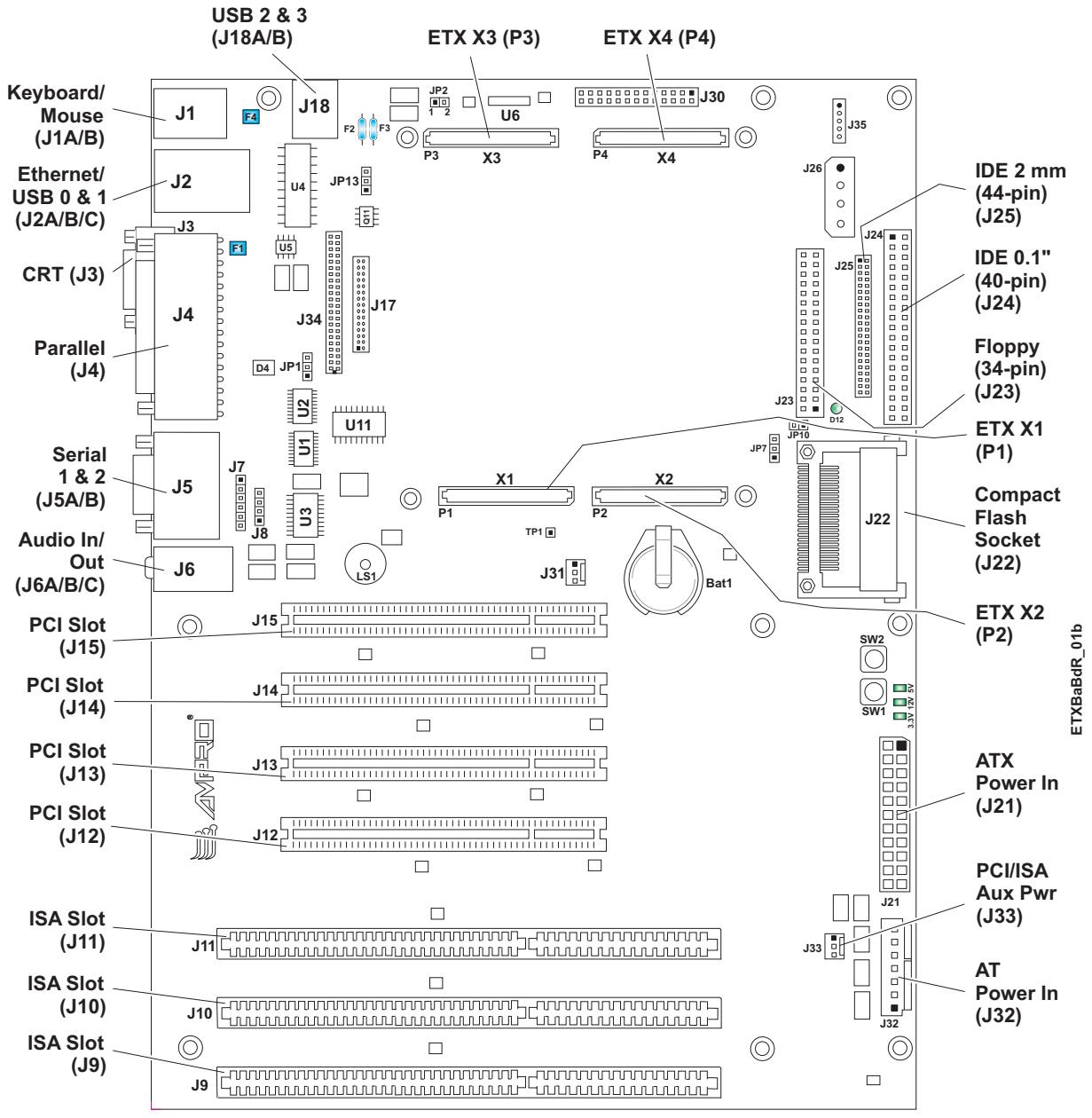
Figure 2-5. Main Connector Locations (Top view)
# NOTE
Ampro uses an identification method in Chapters 3 & 4 to ease connector pin identification. For example, a 20-pin header with two rows of pins, using odd/ even numbering, where pin-2 is directly across and adjacent to pin-1, is noted in this way; 20-pin, two rows, odd/even (1, 2). Alternately, a 20-pin connector using consecutive numbering, where pin-11 is directly across and adjacent to pin-1, is noted in this way; 20-pin, two rows, consecutive (1, 11). The second number in the parenthesis is always directly across from and adjacent to pin-1, with a few exceptions (PCI, ISA, etc.). See Figure 2-6.

Figure 2-6. Connector/Header Pin-Out Identification
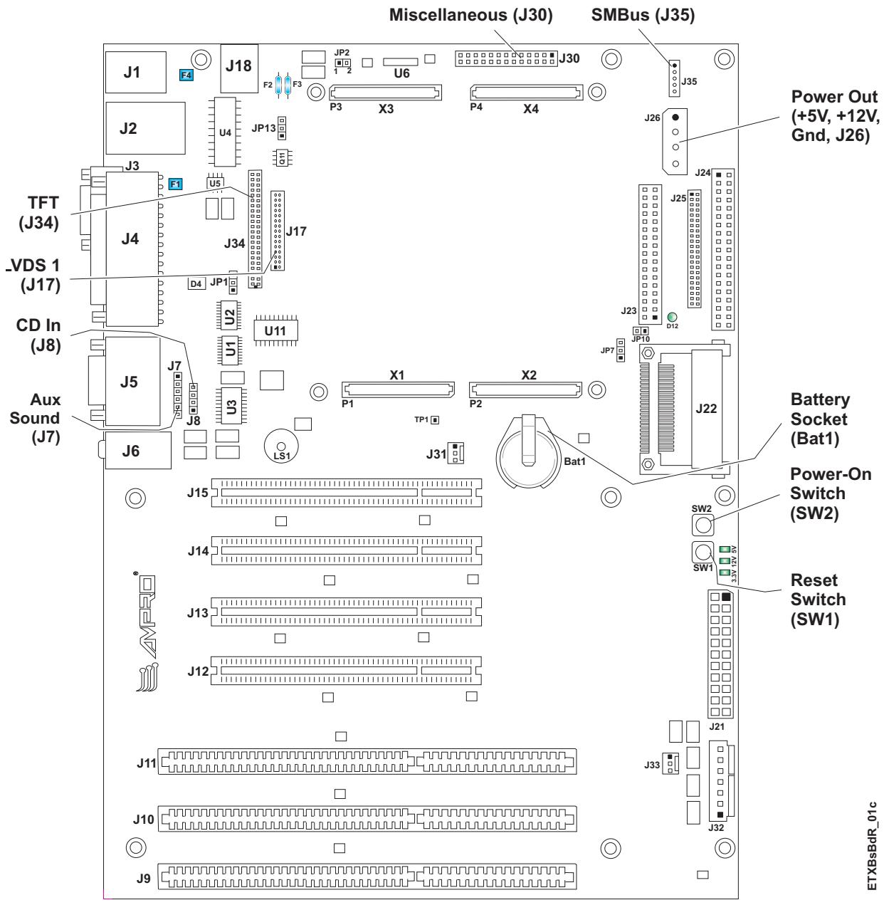
Figure 2-7. Additional Connector and Switch Locations (Top view)
Table 2-3. Fuse and Switch Identification
| Pin # | Signal | Description |
| 1, 2 | GND | Ground |
| 3 | PCICLK3 | PCI clock 3 – This signal line is one of four signal lines. These clock signals provide the timing outputs for four external PCI devices and the timing for all transactions on the PCI bus. |
| 4 | PCICLK4 | PCI clock 4 – Refer to pin-3 for more information. |
| 5, 6 | GND | Ground |
| 7 | PCICLK1 | PCI clock 1 – Refer to pin-3 for more information. |
| 8 | PCICLK2 | PCI clock 2 – Refer to pin-3 for more information. |
| 9 | REQ3* | Bus Request 3 – This signal line is one of four signal lines. These signals indicate to the arbitrator when a device desires use of the bus. |
| 10 | GNT3* | Grant 3 – This signal line is one of four signal lines. These signal lines indicate access has been granted to the requesting device (PCI Masters). |
| 11 | GNT2* | Grant 2 – Refer to pin 10 for more information. |
| 12 | +3.3V | +3.3 volts +/-5% |
| 13 | REQ2* | Bus Request 2 – This signal line is one of three signal lines. These signals notify the arbitrator a device desires use of the bus. |
| 14 | GNT1* | Grant 1 – Refer to pin 10 for more information. |
| 15 | REQ1* | Bus Request 1 – Refer to pin 9 for more information. |
| 16 | +3.3V | +3.3 volts +/-5% |
| 17 | GNT0* | Grant 0 – Refer to pin 10 for more information. |
| 18 | NC | Not Connected (Reserved) |
| 19, 20 | VCC | +5 volts +/-5% |
| 21 | SERIRQ | Serial Interrupt Request – This signal is used to support the serial interrupt protocol. |
| 22 | REQ0* | Bus Request 0 – Refer to pin 9 for more information. |
| 23 | AD0 | Address/Data bus 0 – These signals (AD31 – AD0) are multiplexed on the same PCI connector pins. During the address phase of a PCI cycle, AD31–AD0 contain a 32-bit address or other destination information. During the data phase, AD31 – AD0 contain data. |
| 24 | +3.3V | +3.3 volts +/-5% |
| 25 | AD1 | Address/Data bus 1 – Refer to pin-23 for more information. |
| 26 | AD2 | Address/Data bus 2 – Refer to pin-23 for more information. |
| 27 | AD4 | Address/Data bus 4 – Refer to pin-23 for more information. |
| 28 | AD3 | Address/Data bus 3 – Refer to pin-23 for more information. |
| 29 | AD6 | Address/Data bus 6 – Refer to pin-23 for more information. |
| 30 | AD5 | Address/Data bus 5 – Refer to pin-23 for more information. |
| 31 | CBE0* | PCI Bus Command/Byte Enable 0 – This signal line is one of four signal lines multiplexed on the same pins, so that during the address cycle, the command is defined and during the data cycle, the byte enable is defined. |
| 32 | AD7 | Address/Data bus 7 – Refer to pin-23 for more information. |
| 33 | AD8 | Address/Data bus 8 – Refer to pin-23 for more information. |
| 34 | AD9 | Address/Data bus 9 – Refer to pin-23 for more information. |
| 35, 36 | GND | Ground |
| 37 | AD10 | Address/Data bus 10 – Refer to pin-23 for more information. |
| 38 | AUXAL | Auxiliary A Input Left – This signal is normally used for an external CD-ROM analog output or similar live-level audio source. Minimum input impedance is 5k Ohms and nominal input level is 1 volt RMS. |
| 39 | AD11 | Address/Data bus 11 – Refer to pin-23 for more information. |
| 40 | MIC | Microphone reference signal – This microphone input signal has a minimum input impedance of 5k Ohms, and the maximum input voltage is 0.15 Vp-p. |
| 41 | AD12 | Address/Data bus 12 – Refer to pin-23 for more information. |
| 42 | AUXAR | Auxiliary A Input Right – This signal is normally used for an external CD-ROM analog output or similar live-level audio source. Minimum input impedance is 5k Ohms and nominal input level is 1 volt RMS. |
| 43 | AD13 | Address/Data bus 13 – Refer to pin-23 for more information. |
| 44 | ASVCC | Analog Supply Voltage – This test voltage is used for the sound controller, but is not available for customer use. |
| 45 | AD14 | Address/Data bus 14 – Refer to pin-23 for more information. |
| 46 | SNDL | Stereo Line Output Left channel – This output signal has a nominal level of 1 volt RMS into 10k impedance load. This output signal can not drive low-impedance speakers directly. |
| 47 | AD15 | Address/Data bus 15 – Refer to pin-23 for more information. |
| 48 | ASGND | Analog Ground – This ground is used for the sound controller and an external amplifier to achieve the lowest audio noise levels. |
| 49 | CBE1* | Bus Command and Byte Enable 1 – Refer to pin-31 for more information. |
| 50 | SNDR | Stereo Line Output Right channel – This output signal has a nominal level of 1 volt RMS into 10k impedance load. This output signal can not drive low-impedance speakers directly. |
| 51, 52 | VCC | +5 volts +/-5% |
| 53 | PAR | PCI bus Parity bit – This signal is the even parity bit on AD[31:0] and CBE[3:0]*. |
| 54 | SERR* | System Error – This signal is for reporting address parity errors. |
| 55 | PERR* | Parity Error – This signal is driven by the PCI target during a write to indicate a data parity error has been detected. |
| 56 | RESERVED | Reserved |
| 57 | PME* | Power Management Event – This signal is an optional signal that can be used by a device to request a change in the device or system power state. |
| 58 | USB2- | Universal Serial Bus Port 2 Data Negative |
| 59 | LOCK* | Lock – This signal indicates an operation that may require multiple transactions to complete. |
| 60 | DEVSEL* | Device Select – This signal is driven by the target device when its address is decoded. |
| 61 | TRDY* | Target Ready – This signal indicates the selected device’s ability to complete the current cycle of transaction. Both IRDY* and TRDY* must be asserted to terminate a data cycle. |
| 62 | USB3- | Universal Serial Bus Port 3 Data Negative |
| 63 | IRDY* | Initiator Ready – This signal indicates the master’s ability to complete the current data cycle of the transaction. |
| 64 | STOP* | Stop – This signal is driven by the current PCI target to request the master to stop the current transaction. |
| 65 | FRAME* | PCI bus Frame access – This signal, driven by the current master, indicates the start of a transaction and will remain active until the final data cycle. |
| 66 | USB2 | Universal Serial Bus Port 2 Data Positive |
| 67, 68 | GND | Ground |
| 69 | AD16 | Address/Data bus 16 – Refer to pin-23 for more information. |
| 70 | CBE2* | Bus Command and Byte Enable 2 – Refer to pin-31 for more information. |
| 71 | AD17 | Address/Data bus 17 – Refer to pin-23 for more information. |
| 72 | USB3+ | Universal Serial Bus Port 3 Data Positive |
| 73 | AD19 | Address/Data bus 19 – Refer to pin-23 for more information. |
| 74 | AD18 | Address/Data bus 18 – Refer to pin-23 for more information. |
| 75 | AD20 | Address/Data bus 20 – Refer to pin-23 for more information. |
| 76 | USB0- | Universal Serial Bus Port 0 Data Negative |
| 77 | AD22 | Address/Data bus 22 – Refer to pin-23 for more information. |
| 78 | AD21 | Address/Data bus 21 – Refer to pin-23 for more information. |
| 79 | AD23 | Address/Data bus 23 – Refer to pin-23 for more information. |
| 80 | USB1- | Universal Serial Bus Port 0 Data Negative |
| 81 | AD24 | Address/Data bus 24 – Refer to pin-23 for more information. |
| 82 | CBE3* | Bus Command and Byte Enable 3 – Refer to pin-31 for more information. |
| 83, 84 | VCC | +5 volts +/-5% |
| 85 | AD25 | Address/Data bus 25 – Refer to pin-23 for more information. |
| 86 | AD26 | Address/Data bus 26 – Refer to pin-23 for more information. |
| 87 | AD28 | Address/Data bus 28 – Refer to pin-23 for more information. |
| 88 | USB0+ | Universal Serial Bus Port 0 Data Positive |
| 89 | AD27 | Address/Data bus 27 – Refer to pin-23 for more information. |
| 90 | AD29 | Address/Data bus 29 – Refer to pin-23 for more information. |
| 91 | AD30 | Address/Data bus 30 – Refer to pin-23 for more information. |
| 92 | USB1+ | Universal Serial Bus Port 1 Data Positive |
| 93 | PCIRST* | PCI Bus Reset – This output signal is used to reset the entire PCI Bus and is asserted during a system reset. |
| 94 | AD31 | Address/Data bus 31 – Refer to pin-23 for more information. |
| 95 | INTC* | Interrupt C – This signal is used to request an interrupt and only has meaning on a multi-function device. |
| 96 | INTD* | Interrupt D – This signal is used to request an interrupt and only has meaning on a multi-function device. |
| 97 | INTA* | Interrupt A – This signal is used to request an interrupt. |
| 98 | INTB* | Interrupt B – This signal is used to request an interrupt and only has meaning on a multi-function device. |
| 99 | GND | Ground |
| 100 | GND | Ground |
# X2 ISA Bus Interface
The X2 connector (P2) only supports the ISA Bus interface. Table 3-2 provides the complete pin/signals for the X2 connector, which has 100 pins, 2 rows, odd/even (1, 2) with 0.6 mm pin spacing.
Table 3-2. ETX Baseboard X2 Interface Pin/Signal Descriptions (P2)
Notes: The shaded area denotes power or ground. The signals marked with \* = Negative true logic.
| Pin # | Signal | Description |
| 1, 2 | GND | Ground |
| 3 | SD14 | System Data 14 – This signal (0 to 19) provides a system data bit. |
| 4 | SD15 | System Data 15 – Refer to SD14, pin-3, for more information. |
| 5 | SD13 | System Data 13 – Refer to SD14, pin-3, for more information. |
| 6 | Master* | Bus Master* – This signal is used by an ISA board along with a DRQ line to gain ownership of the ISA bus. |
| 7 | SD12 | System Data 12 – Refer to SD14, pin-3, for more information. |
| 8 | DREQ7 | DMA Request 7 – Used by I/O resources to request DMA service. Must be held high until associated DACK7 line is active. |
| 9 | SD11 | System Data 11 – Refer to SD14, pin-3, for more information. |
| 10 | DACK7* | DMA Acknowledge 1 – Used by DMA controller to select the I/O resource requesting the bus, or to request ownership of the bus as a bus master device. Can also be used by the ISA bus master to gain control of the bus from the DMA controller. |
| 11 | SD10 | System Data 10 – Refer to SD14, pin-3, for more information. |
| 12 | DREQ6 | DMA Request 6 – Used by I/O resources to request DMA service. Must be held high until associated DACK6 line is active. |
| 13 | SD9 | System Data 9 – Refer to SD14, pin-3, for more information. |
| 14 | DACK6* | DMA Acknowledge 1 – Used by DMA controller to select the I/O resource requesting the bus, or to request ownership of the bus as a bus master device. Can also be used by the ISA bus master to gain control of the bus from the DMA controller. |
| 15 | SD8 | System Data 8 – Refer to SD14, pin-3, for more information. |
| 16 | DREQ5 | DMA Request 5 – Used by I/O resources to request DMA service. Must be held high until associated DACK5 line is active. |
| 17 | MEMW* | Memory Write – This signal instructs a selected memory device to store data currently on the data bus. It is active on all memory write cycles. |
| 18 | DACK5* | DMA Acknowledge 1 – Used by DMA controller to select the I/O resource requesting the bus or to request ownership of the bus as a bus master device. Can also be used by the ISA bus master to gain control of the bus from the DMA controller. |
| 19 | MEMR* | Memory Read – This signal instructs a selected memory device to drive data onto the data bus. It is active on all memory read cycles. |
| 20 | DREQ0 | DMA Request 0 – Used by I/O resources to request DMA service. Must be held high until associated DACK0 line is active. |
| 21 | LA17 | Latchable Address 17 – These signals (LA 17-23) must be latched by the resource if these lines are required for the entire data cycle. |
| 22 | DACK0* | DMA Acknowledge 0 – Used by DMA controller to select the I/O resource requesting the bus, or to request ownership of the bus as a bus master device. Can also be used by the ISA bus master to gain control of the bus from the DMA controller. |
| 23 | LA18 | Latchable Address 18 – Refer to LA17, pin-21, for more information. |
| 24 | IRQ14 | Interrupt Request 14 – Asserted by a device when it has pending interrupt request. Only one device may use the request line at a time. |
| 25 | LA19 | Latchable Address 19 – Refer to LA17, pin-21, for more information. |
| 26 | IRQ15 | Interrupt Request 15 – Asserted by a device when it has pending interrupt request. Only one device may use the request line at a time. |
| 27 | LA20 | Latchable Address 20 – Refer to LA17, pin-21, for more information. |
| 28 | IRQ12 | Interrupt Request 12 – Asserted by a device when it has pending interrupt request. Only one device may use the request line at a time. |
| 29 | LA21 | Latchable Address 21 – Refer to LA17, pin-21, for more information. |
| 30 | IRQ11 | Interrupt Request 11 – Asserted by a device when it has pending interrupt request. Only one device may use the request line at a time. |
| 31 | LA22 | Latchable Address 22 – Refer to LA17, pin-21, for more information. |
| 32 | IRQ10 | Interrupt Request 10 – Asserted by a device when it has pending interrupt request. Only one device may use the request line at a time. |
| 33 | LA23 | Latchable Address 23 – Refer to LA17, pin-21, for more information. |
| 34 | IO16* | I/O Chip Select 16 – This signal is driven low by an I/O slave device to indicate it is capable of performing a 16-bit I/O data transfer. This signal is driven from a decode of the SA15 to SA0 address lines. |
| 35, 36 | GND | Ground |
| 37 | SBHE* | System Byte High Enable – This signal is driven low to indicate a transfer of data on the high half of the data bus (D15 to D8). |
| 38 | M16* | Memory Chip Select 16 – This signal is driven low by a memory slave device to indicate it is capable of performing a 16-bit memory data transfer. This signal is driven from a decode of the LA23 to LA17 address lines. |
| 39 | SA0 | System Address 0 – These signals (0 to 19) provide system address bits. |
| 40 | OSC | Oscillator – This clock signal operates at 14.3MHz. This signal is not synchronous with the system clock (SYSCLK). |
| 41 | SA1 | System Address 1 – Refer to SA0, pin-39, for more information. |
| 42 | BALE | Buffered Address Latch Enable – This signal is active-high pulse generated at the beginning of any bus cycle initiated by a CPU module. It indicates when the SA[0..19], LA[17..23] AEN, an SBHE# signals are valid. |
| 43 | SA2 | System Address 2 – Refer to SA0, pin-39, for more information. |
| 44 | TC | Terminal Count – This signal is a pulse to indicate a terminal count has been reached on a DMA channel operation. |
| 45 | SA3 | System Address 3 – Refer to SA0, pin-39, for more information. |
| 46 | DACK2* | DMA Acknowledge 2 – Used by DMA controller to select the I/O resource requesting the bus, or to request ownership of the bus as a bus master device. Can also be used by the ISA bus master to gain control of the bus from the DMA controller. |
| 47 | SA4 | System Address 1 – Refer to SA0, pin-39, for more information. |
| 48 | IRQ3 | Interrupt Request 3 – Asserted by a device when it has pending interrupt request. Only one device may use the request line at a time. |
| 49 | SA5 | System Address 1 – Refer to SA0, pin-39, for more information. |
| 50 | IRQ4 | Interrupt Request 4 – Asserted by a device when it has pending interrupt request. Only one device may use the request line at a time. |
| 51, 52 | VCC | +5V +/- 5% |
| 53 | SA6 | System Address 6 – Refer to SA0, pin-39, for more information. |
| 54 | IRQ5 | Interrupt Request 5 – Asserted by a device when it has pending interrupt request. Only one device may use the request line at a time. |
| 55 | SA7 | System Address 7 – Refer to SA0, pin-39, for more information. |
| 56 | IRQ6 | Interrupt Request 6 – Asserted by a device when it has pending interrupt request. Only one device may use the request line at a time. |
| 57 | SA8 | System Address 8 – Refer to SA0, pin-39, for more information. |
| 58 | IRQ7 | Interrupt Request 7 – Asserted by a device when it has pending interrupt request. Only one device at a time may use the request line. |
| 59 | SA9 | System Address 9– Refer to SA0, pin-39, for more information. |
| 60 | SYSCLK | System Clock – This is a free running clock typically in the 8MHZ to 10MHz range, although its exact frequency is not guaranteed. |
| 61 | SA10 | System Address 10 – Refer to SA0, pin-39, for more information. |
| 62 | REFSH* | Memory Refresh – This signal is driven low to indicate a memory refresh cycle is in progress. Memory is refreshed every 15.6 usec. |
| 63 | SA11 | System Address 10 – Refer to SA0, pin-39, for more information. |
| 64 | DREQ1 | DMA Request 1 – Used by I/O resources to request DMA service. Must be held high until associated DACK1 line is active. |
| 65 | SA12 | System Address 12 – Refer to SA0, pin-39, for more information. |
| 66 | DACK1* | DMA Acknowledge 1 – Used by DMA controller to select the I/O resource requesting the bus or to request ownership of the bus as a bus master device. Can also be used by the ISA bus master to gain control of the bus from the DMA controller. |
| 67, 68 | GND | Ground |
| 69 | SA13 | System Address 13 – Refer to SA0, pin-39, for more information. |
| 70 | DREQ3 | DMA Request 3 – Used by I/O resources to request DMA service. Must be held high until associated DACK3 line is active. |
| 71 | SA14 | System Address 14 – Refer to SA0, pin-39, for more information. |
| 72 | DACK3* | DMA Acknowledge 3 – Used by DMA controller to select the I/O resource requesting the bus, or to request ownership of the bus as a bus master device. Can also be used by the ISA bus master to gain control of the bus from the DMA controller. |
| 73 | SA15 | System Address 15 – Refer to SA0, pin-39, for more information. |
| 74 | IOR* | I/O Read – This strobe signal is driven by the owner of the bus (ISA bus master or DMA controller) and instructs the selected I/O device to drive read data onto the data bus. |
| 75 | SA16 | System Address 16 – Refer to SA0, pin-39, for more information. |
| 76 | IOW* | I/O Write – This strobe signal is driven by the owner of the bus (ISA bus master or DMA controller) and instructs the selected I/O device to capture the write data on the data bus. |
| 77 | SA18 | System Address 18 – Refer to SA0, pin-39, for more information. |
| 78 | SA17 | System Address 17 – Refer to SA0, pin-39, for more information. |
| 79 | SA19 | System Address 19 – Refer to SA0, pin-39, for more information. |
| 80 | SMEMR* | System Memory Read – This signal is used by bus owner to request a memory device to drive data onto the data bus and only active for lower 1 MB. Used for legacy compatibility with 8-bit cards. |
| 81 | IOCHRDY | I/O Channel Ready – This signal allows slower ISA boards to lengthen I/O or memory cycles by inserting wait states. This signal's normal state is active high (ready). ISA boards drive the signal inactive low (not ready) to insert wait states. Devices using this signal to insert wait states should drive it low immediately after detecting a valid address decode and an active read or write command. Signal goes high when the device is ready to complete the cycle. |
| 82 | AEN | Address Enable – This signal is reserved for the ISA Bus and is asserted during DMA cycles to prevent I/O slaves from misinterpreting DMA cycles as valid I/O cycles. |
| 83, 83 | VCC | +5V +/- 5% |
| 85 | SD0 | System Data 0 – Refer to SD14, pin-3, for more information. |
| 86 | SMEMW* | System Memory Write – This signal is used by bus owner to request a memory device to store data currently on the data bus and only active for the lower 1 MB. Used for legacy compatibility with 8-bit cards. |
| 87 | SD2 | System Data 2 – Refer to SD14, pin-3, for more information. |
| 88 | SD1 | System Data 1 – Refer to SD14, pin-3, for more information. |
| 89 | SD3 | System Data 3 – Refer to SD14, pin-3, for more information. |
| 90 | NOWS* | No Wait State – This signal is driven low by a bus slave device to indicate it is capable of performing a bus cycle without inserting any additional wait states. To perform a 16-bit memory cycle without wait states, this signal is derived from an address decode. |
| 91 | DREQ2 | DMA Request 2 – Used by I/O resources to request DMA service. Must be held high until associated DACK2 line is active. |
| 92 | SD4 | System Data 4 – Refer to SD14, pin-3, for more information. |
| 93 | SD5 | System Data 5 – Refer to SD14, pin-3, for more information. |
| 94 | IRQ9 | Interrupt Request 9 – Asserted by a device when it has pending interrupt request. Only one device may use the request line at a time. |
| 95 | SD6 | System Data 6 – Refer to SD14, pin-3, for more information. |
| 96 | SD7 | System Data 7 – Refer to SD14, pin-3, for more information. |
| 97 | IOCHK* | I/O Channel Check – This active low input signal indicates an error has occurred on the module bus. If I/O checking is enable on the CPU module, an IOCHK# assertion by a peripheral device will send a non-maskable interrupt (NMI) to the processor. |
| 98 | RSTDRV | Reset Drive – This signal is used to reset or initialize system logic on power up or subsequent system reset. |
| 99 | GND | Ground |
| 100 | GND | Ground |
# X3 Primary I/O Interface
The X3 connector (P3) is used for Floppy or Printer port (LPT1), Serial ports (COM1 and COM2) Mouse and Keyboard interfaces, Infrared (IrDA) port, and the video interfaces for standard CRT video and LVDS ports with flat panel controls. See Table 3-3 for the complete X3 connector pin/signals, which has 100 pins, 2 rows, odd/even (1, 2) with 0.6 mm pin spacing.
Table 3-3. ETX Baseboard X3 Interface Pin/Signal Descriptions (P3)
Notes: The shaded area denotes power or ground. The signals marked with \* = Negative true logic.
| Pin # | Signal | Description |
| 1, 2 | GND | Ground |
| 3 | R | Red – This is the Red analog output signal to the CRT and requires 75 ohm termination to ground at the video connector. |
| 4 | B | Blue – This is the Blue analog output signal to the CRT and requires 75 ohm termination to ground at the video connector. |
| 5 | HSY | Horizontal Sync – This signal is used for the digital horizontal sync output to the CRT monitor. |
| 6 | G | Green – This is the Green analog output signal to the CRT and requires 75 ohm termination to ground at the video connector. |
| 7 | VSY | Vertical Sync – This signal is used for the digital vertical sync output to the CRT monitor. |
| 8 | DDCK | Display Data Channel Clock – This signal line provides the data clock signal to the Northbridge from the monitor. This is part of the Plug and Play standard developed by the VESA trade association. |
| 9 | DETECT* | Panel Hot-Plug Detection – Implementation of this pin is optional. |
| 10 | DDDA | Display Data Channel Data – This signal line provides information to the Northbridge about the monitor type, brand, model. This is part of the Plug and Play standard developed by the VESA trade association. |
| 11 | LCDDO16 | LCD Data Output 16 – These signal lines <8-19> provide LVDS support for two channels. See pin-29 for LVDS single channel support. |
| 12 | LCDDO18 | LCD Data Output 18 – This pin and pin-14 only are used for 24-bit panels (Txout3+ and Txout3-) in a two-channel LVDS configuration. |
| 13 | LCDDO17 | LCD Data Output 17 – Refer to pin-11 LCDDO16 for more information. |
| 14 | LCDDO19 | LCD Data Output 19 – This pin and pin-12 only are used for 24-bit panels (Txout3+ and Txout3-) in a two-channel LVDS configuration. |
| 15, 16 | GND | Ground |
| 17 | LCDDO13 | LCD Data Output 13 – Refer to pin-11 LCDDO16 for more information. |
| 18 | LCDDO15 | LCD Data Output 15 – Refer to pin-11 LCDDO16 for more information. |
| 19 | LCDDO12 | LCD Data Output 12 – Refer to pin-11 LCDDO16 for more information. |
| 20 | LCDDO14 | LCD Data Output 14 – Refer to pin-11 LCDDO16 for more information. |
| 21, 22 | GND | Ground |
| 23 | LCDDO8 | LCD Data Output 8 – This pin and pin-25 only are used for 24-bit panels (Txout3+ and Txout3-) in a single channel LVDS configuration. |
| 24 | LCDDO11 | LCD Data Output 11 – Refer to pin-11 LCDDO16 for more information. |
| 25 | LCDDO9 | LCD Data Output 9 – This pin and pin-23 only are used for 24-bit panels (Txout3+ and Txout3-) in a single channel LVDS configuration. |
| 26 | LCDD10 | LCD Data Output 10 – Refer to pin-11 LCDDO16 for more information. |
| 27, 28 | GND | Ground |
| 29 | LCDDO4 | LCD Data Output 4 – These signal lines <0-7> provide minimum LVDS support. These four signal pairs can support a single channel TFT interface of 18 bits or less. Single channel LVDS links use the first of the two channels only. Dual channel links, which are commonly used to transmit high data rates, will use both the first and second channels. |
| 30 | LCDDO7 | LCD Data Output 7 – Refer to pin-29 LCDDO4 for more information. |
| 31 | LCDDO5 | LCD Data Output 5 – Refer to pin-29 LCDDO4 for more information. |
| 32 | LCDDO6 | LCD Data Output 6 – Refer to pin-29 LCDDO4 for more information. |
| 33, 34 | GND | Ground |
| 35 | LCDDO1 | LCD Data Output 1 – Refer to pin-29 LCDDO4 for more information. |
| 36 | LCDDO3 | LCD Data Output 3 – Refer to pin-29 LCDDO4 for more information. |
| 37 | LCDDO0 | LCD Data Output 0 – Refer to pin-29 LCDDO4 for more information. |
| 38 | LCDDO2 | LCD Data Output 2 – Refer to pin-29 LCDDO4 for more information. |
| 39, 40 | VCC | +5V +/- 5% |
| 41 | FP_I2C_DAT | Flat Panel I2C Data – This I2C data interface to the panel parameter EEPROM used with the flat panel, allows the ETX module to set the proper timing parameter in a specific LCD panel. |
| 42 | LTGIO0 | General Purpose I/O – This pin is not used by flat panel interface. |
| 43 | FP_I2C_CLK | Flat Panel I2C Clock – This I2C clock signal is needed when setting parameters in the panel parameter EEPROM used with the flat panel. |
| 44 | BLON* | Backlight On – This signal controls the external backlight power for the flat panel. |
| 45 | BIASON | BIAS ON – This signal controls the flat panel contrast voltage. |
| 46 | DIGON | Digital Power On – This signal controls the digital flat panel power up. |
| 47 | COMP | Composite Analog Output – Not supported at this time. |
| 48 | Y | Y Analog S-Video Output – Not supported at this time. |
| 49 | SYNC | Composite Sync – Not supported at this time. |
| 50 | C | C Analog S-Video Output – Not supported at this time. |
| 51 | LPT/FLPY* | Parallel/Floppy Select – This ETX input signal selects the parallel or floppy port signal. If this signal is Low at boot time, the floppy drive is selected. If this signal is High at boot time, the parallel port is selected. This state can not be changed until the next boot cycle. |
| 52 | NC | Not Connected (Reserved) |
| 53 | VCC | +5V +/- 5% |
| 54 | GND | Ground |
| 55 | Strobe* | Parallel Strobe* – This output signal is used to strobe data into the printer. I/O pin in ECP/EPP mode. |
| DS0* | Floppy Drive Select 0 – Selects drive 0. |
| 56 | AFD* | Parallel Auto Feed * – This is a output signal from the printer to automatically feed one line after each line is printed. |
| DENSEL | Floppy Drive Density Select – This signal indicates if a low (250/300kBps) or high (500/1kBps) data rate is selected. |
| 57 | NC | Not Connected (Reserved) |
| 58 | PD7 | Parallel Port Data 7 – This signal (0 to 7) provides a parallel port data signal and is the printer data MSB. |
| 59 | IRRX | IR Receive Data (HPSIR or ASKIR) |
| 60 | ERR* | Parallel Error – This is a status output signal from the printer. A low state indicates an error condition on the printer. |
| HDSEL* | Floppy Head Select – Selects side for Read/Write operations (0 = side 1, 1 = side 0). |
| 61 | IRTX | IR Transmit Data (HPSIR or ASKIR) |
| 62 | PD6 | Parallel Port Data 6 – Refer to pin-58 and 80 for more information. |
| MTR0* | Floppy Motor Control 0 – Select motor on drive 0. |
| 63 | RXD2 | Receive Data 2 – Serial port 2 receive data in |
| 64 | INIT* | Parallel Initialize – This signal initializes the printer. Output in standard mode, I/O in ECP/EPP mode. |
| DIR* | Floppy Direction – Direction of head movement (0 = inward motion, 1 = outward motion). |
| 65, 66 | GND | Ground |
| 67 | RTS2* | Request To Send 2 – Indicates Serial port 2 is ready to transmit data. Used as hardware handshake with CTS2 for low level flow control. |
| 68 | PD5 | Parallel Port Data 5 – Refer to pin-58 and 80 for more information. |
| 69 | DTR2* | Data Terminal Ready 2 – Indicates Serial port 2 is powered, initialized, and ready. Used as hardware handshake with DSR2 for overall readiness. |
| 70 | SLCTIN | Select In – This output signal is used to select the printer. I/O pin in ECP/EPP mode. |
| STEP* | Floppy Step – Low pulse for each track-to-track movement of the head. |
| 71 | DCD2* | Data Carrier Detect 2 – Indicates external serial device is detecting a carrier signal (i.e., a communication channel is currently open). In direct connect environments, this input is driven by DTR2 as part of the DTR2/DSR2 handshake. |
| 72 | PD4 | Parallel Port Data 4 – Refer to pin-58 and 80 for more information. |
| DSKCHG* | Floppy Disk Change – Senses the drive door is open or the diskette has been changed since the last drive selection. |
| 73 | DSR2* | Data Set Ready 2 – Indicates external serial device is powered, initialized, and ready. Used as hardware handshake with DTR2 for overall readiness. |
| 74 | PD3 | Parallel Port Data 3 – Refer to pin-58 and 80 for more information. |
| RDATA* | Floppy Read Data – Raw serial bit stream from drive for read operations. |
| 75 | CTS2* | Clear To Send 2 – Indicates external serial device is ready to receive data. Used as hardware handshake with RTS2 for low level flow control. |
| 76 | PD2 | Parallel Port Data 2 – Refer to pin-58 and 80 for more information. |
| WP* | Floppy Write Protect – Senses the diskette is write protected. |
| 77 | TXD2 | Transmit Data 2 – Serial port 2 transmit data out |
| 78 | PD1 | Parallel Port Data 1 – Refer to pin-58 and 80 for more information. |
| TRK0* | Floppy Track 0 – Sense detects the head is positioned over track 0. |
| 79 | RI2* | Ring Indicator 2 – Indicates external serial device is detecting a ring condition. Used by software to initiate operations to answer and then open the communications channel. |
| 80 | PD0INDEX* | Parallel Port Data 0 – This pin (0 to 7) provides a parallel port data signal and is the printer data LSB.Floppy Index – Sense to detect that the head is positioned over the beginning of a track. |
| 81, 82 | VCC | +5V +/- 5% |
| 83 | RXD1* | Receive Data 1 – Serial port 1 receive data in. |
| 84 | ACK*DRV1 | Parallel Acknowledge * – This is a status input signal from the printer. A Low State indicates it has received the data and is ready to accept new data.Floppy Drive Select 1 – This signal selects drive 1. |
| 85 | RTS1* | Request To Send 1 – Indicates Serial port 1 is ready to transmit data. Used as hardware handshake with CTS1 for low level flow control. |
| 86 | BUSYMTR1 | Parallel Busy – This is a status input signal from the printer. A high state indicates the printer is not ready to accept data.Floppy Motor Control 1 – This signal selects motor on drive 1. |
| 87 | DTR1* | Data Terminal Ready 1 – Indicates Serial port 1 is powered, initialized, and ready. Used as hardware handshake with DSR1 for overall readiness. |
| 88 | PEWDATA* | Parallel Paper End – This is a status input signal from the printer. A high state indicates it is out of paper.Floppy Write Data – Encoded data to the drive for write operations. |
| 89 | DCD1* | Data Carrier Detect 1 – Indicates external serial device is detecting a carrier signal (i.e., a communication channel is currently open). In direct connect environments, this input is driven by DTR1 as part of the DTR1/DSR1 handshake. |
| 90 | SLCTWGATE* | Parallel Select – This is a status output signal from the printer. A high state indicates it is selected and powered on.Floppy Write Gate – Signals drive to enable current flow in the write head. |
| 91 | DSR1* | Data Set Ready 1 – Indicates external serial device is powered, initialized, and ready. Used as hardware handshake with DTR1 for overall readiness. |
| 92 | MSCLK | Mouse Clock signal – This signal clocks the data from the mouse. |
| 93 | CTS1* | Request To Send 1 – Indicates Serial port 1 is ready to transmit data. Used as hardware handshake with CTS1 for low level flow control. |
| 94 | MSDAT | Mouse Data signal – This signal provides the mouse data. |
| 95 | TXD1 | Transmit Data 1 – Serial port 1 transmit data out |
| 96 | KBCLK | Keyboard Clock signal – This signal clocks the data from the keyboard. |
| 97 | RI1* | Ring Indicator 1 – Indicates external serial device is detecting a ring condition. Used by software to initiate operations to answer and then open the communications channel. |
| 98 | KBDAT | Keyboard Data signal – This signal provides the keyboard data. |
| 99 | GND | Ground |
| 100 | GND | Ground |
# X4 IDE and Auxiliary Interface
The X4 connector (P4) is used for Primary IDE, Ethernet port, RTC/Battery, PC speaker, power management, SMBus, and I2 C interfaces. Table 3-4 provides the complete pin/signals for the X4 connector, which has 100 pins, 2 rows, odd/even (1, 2) with 0.6 mm pin spacing.
Notes: The shaded area denotes power or ground. The signals marked with \* = Negative true logic.
Table 3-4. ETX Baseboard X4 Interface Pin/Signal Descriptions (P4)
| Pin # | Signal | Description |
| 1, 2 | GND | Ground |
| 3 | 5V_SB | 5 volt Suspend – This control signal is sent to the ATX power supply for a suspend or standby state. |
| 4 | PWGIN | Power Good In – This active high input signal indicates to the ETX Baseboard, the power is good and it can begin the boot process. |
| 5 | PS_ON | Power Supply On – This active-low output signal from the ETX Baseboard is sent to the ATX power supply to turn it on. |
| 6 | SPEAKER | Speaker – This PC speaker output signal must be connected to a speaker (piezoelectric or dynamic) on the baseboard to hear the output (beeps). |
| 7 | PWRBTN* | Power Button – This signal provides a momentary ground through an open collector driver to the ATX power supply to change states (turn it on). |
| 8 | BATT | Battery Voltage – This is the + battery connection to baseboard for +3 volt lithium backup battery used for RTC operation and CMOS non-volatile memory. |
| 9 | KBINH | Keyboard Inhibit – Asserting this pin disables data input from the keyboard. Not supported on all ETX modules. |
| 10 | LILED | Link Integrity LED – The LINK LED pin indicates link integrity. If the link is valid in either 10 Mbps or 100 Mbps, the LED is on; if the link is invalid, the LED is off. |
| 11 | RSMRST* | Resume Reset – This signal is driven low by external circuitry to reset the power management logic on the ETX Baseboard. |
| 12 | ACTLED | Activity LED – The Activity LED pin indicates either transmit or receive activity. When activity is present, the activity LED is on; when no activity is present, the activity LED is off. |
| 13 | ROMKBCS* | Reserved – Do not connect to this pin. |
| 14 | SPDLED | Speed LED – The speed LED pin indicates the speed. The speed LED will be on at 100 Mbps and off at 10 Mbps. |
| 15 | EXT_PRG | Reserved – Do not connect to this pin. |
| 16 | I2C_CLK | I2C Clock – This clock signal supports external I2C devices. |
| 17, 18 | VCC | +5 volts +/-5% |
| 19 | OVCR* | Over Current Detect – This signal indicates a USB over-current condition. |
| 20 | GPCS* | Reserved – Do not connect to this pin. |
| 21 | EXTSMI* | Extern System Management Interrupt – This signal is provided by external circuitry to initiate an SMI event with the ETX Baseboard. |
| 22 | I2C_DAT | I2C Data – This data signal supports external I2C devices. |
| 23 | SMBCLK | System Management Bus Clock – This signal is used to support internal and external SMBus devices, such as temperature and battery monitoring. |
| 24 | SMBDATA | System Management Bus Data – This signal is used to support internal and external SMBus devices, such as temperature and battery monitoring. |
| 25 | SIDE_CS3* | Not connected. |
| 26 | SMBALRT* | System Management Bus Alert - This signal is used by SMBus devices to signal an event on the SMBus. |
| 27 | SIDE_CS1* | Not Connected. |
| 28 | DASP_S | Drive Active/Drive Present - This signal is time-multiplexed and indicates the drive is active. Also used for Master/Slave negotiation on the Primary IDE channel. If a compact flash is connected to the baseboard, this signal must be routed to the DASP_S pin of any other device connected to the Primary IDE channel. |
| 29 | SIDE_A2 | Not connected. |
| 30 | PIDE_CS3* | Primary Chip Select 3 - Used to select the host-accessible Command Block Register. |
| 31 | SIDE_A0 | Not connected. |
| 32 | PIDE_CS1* | Primary Chip Select 1 - Used to select the host-accessible Command Block Register. |
| 33, 34 | GND | Ground |
| 35 | PDIAG_S | Passed Diagnostics - This signal is used for Master/Slave negotiation on the Primary IDE channel. It is asserted by the Slave to indicate to master that the slave has passed its internal Diagnostics command. If a compact flash is connected to the baseboard, this signal must be routed to the DASP_S pin of any another device connected to the Primary IDE channel.May also be used to detect the presence of an 80 conductor IDE cable, which is required for support of the DMA66 or DMA100 high-speed transfers. |
| 36 | PIDE_A2 | Primary Drive Address Bus 2 - Used (0 to 2) to indicate which byte in the ATA command block or control block (register) is being accessed. |
| 37 | SIDE_A1 | Not connected. |
| 38 | PIDE_A0 | Primary Drive Address Bus 0 - Refer to PIDE_A2, pin-36, for more information. |
| 39 | SIDE_INTRQ | Not connected. |
| 40 | PIDE_A1 | Primary Drive Address Bus 1 - Refer to PIDE_A2, pin-36, for more information. |
| 41 | BATLOW* | Battery Low - This external signal to the ETX Baseboard indicates when the external battery is low. |
| 42 | GPE1* | General Purpose Power Management Event input 1 - This signal is driven by external circuitry to indicate an external power management event. This pin is commonly connected to the chipset's LID# input. |
| 43 | SIDE_AK* | Not connected. |
| 44 | PIDE_INTRQ | Primary Drive Interrupt Request (IRQ 14)- Asserted by drive when it has pending interrupt (PIO transfer of data to or from the drive to the host). |
| 45 | SIDE_RDY | Not connected. |
| 46 | PIDE_AK* | Primary DMA Channel Acknowledge - Used by the host to acknowledge data has been accepted or data is available. Used in response to PIDE_DMARQ asserted. |
| 47 | SIDE_IOR* | Not connected. |
| 48 | PIDE_RDY | Primary I/O Channel Ready - When negated extends the host transfer cycle of any host register access when the drive is not ready to respond to a data transfer request. High impedance if asserted. |
| 49, 50 | VCC | +5 volts +/-5% |
| 51 | SIDE_IOW* | Not connected. |
| 52 | PIDE_IOR* | Primary Drive I/O Read – Primary strobe signal for read functions. Negative edge enables data from a register or data port of the drive onto the host data bus. Positive edge latches data at the host. |
| 53 | SIDE_DRQ | Not connected. |
| 54 | PIDE_IOW* | Primary Drive I/O Write – Primary strobe signal for write functions. Negative edge enables data from a register or data port of the drive onto the host data bus. Positive edge latches data at the host. |
| 55 | SIDE_D15 | Not connected. |
| 56 | PIDE_DRQ | Primary DMA Request – Used for DMA transfers between host and drive (direction of transfer controlled by IOR* and IOW*). Also used in an asynchronous mode with ACK*. Drive asserts an IRQ when ready to transfer or receive data. |
| 57 | SIDE_D0 | Not connected. |
| 58 | PIDE_D15 | Primary Disk Data 15 – These signals (0 to 15) provide the Primary IDE disk data signals. |
| 59 | SIDE_D14 | Not connected. |
| 60 | PIDE_D0 | Primary Disk Data 0 – Refer to pin-58 for more information. |
| 61 | SIDE_D1 | Not connected. |
| 62 | PIDE_D14 | Primary Disk Data 14 – Refer to pin-58 for more information. |
| 63 | SIDE_D13 | Not connected. |
| 64 | PIDE_D1 | Primary Disk Data 1 – Refer to pin-58 for more information. |
| 65, 66 | GND | Ground |
| 67 | SIDE_D2 | Not connected. |
| 68 | PIDE_D13 | Primary Disk Data 13 – Refer to pin-58 for more information. |
| 69 | SIDE_D12 | Not connected. |
| 70 | PIDE_D2 | Primary Disk Data 2 – Refer to pin-58 for more information. |
| 71 | SIDE_D3 | Not connected. |
| 72 | PIDE_D12 | Primary Disk Data 12 – Refer to pin-58 for more information. |
| 73 | SIDE_D11 | Not connected. |
| 74 | PIDE_D3 | Primary Disk Data 3 – Refer to pin-58 for more information. |
| 75 | SIDE_D4 | Not connected. |
| 76 | PIDE_D11 | Primary Disk Data 11 – Refer to pin-58 for more information. |
| 77 | SIDE_D10 | Not connected. |
| 78 | PIDE_D4 | Primary Disk Data 4 – Refer to pin-58 for more information. |
| 79 | SIDE_D5 | Not connected. |
| 80 | PIDE_D10 | Primary Disk Data 10 – Refer to pin-58 for more information. |
| 81, 82 | VCC | +5 volts +/-5% |
| 83 | SIDE_D9 | Not connected. |
| 84 | PIDE_D5 | Primary Disk Data 5 – Refer to pin-58 for more information. |
| 85 | SIDE_D6 | Not connected. |
| 86 | PIDE_D9 | Primary Disk Data 9 – Refer to pin-58 for more information. |
| 87 | SIDE_D8 | Not connected. |
| 88 | PIDE_D6 | Primary Disk Data 6 – Refer to pin-58 for more information. |
| 89 | GPE2* | General Purpose Power Management Event input 2 – This signal is driven by external circuitry to indicate an external power management event. This pin is commonly connected to the chipset's RING# input. |
| 90 | CBLID_P* | Primary Cable ID Select – Used to detects the presence of an 80 conductor IDE cable on the primary IDE channel. This allows BIOS or system software to determine if is necessary to enable the high-speed transfer modes (DMA66 or DMA100). |
| 91 | RXD- | Half of Ethernet Analog Twisted Pair Receive Differential Pair – This pin and pin-93 make up the Receive twisted pair and receive the serial bit stream on the Unshielded Twisted Pair Cable (UTP). |
| 92 | PIDE_D8 | Primary Disk Data 8 – Refer to pin-58 for more information. |
| 93 | RXD+ | Part of Ethernet Analog Twisted Pair Receive Differential Pair – Refer to pin-91 for more information. |
| 94 | SIDE_D7 | Not connected. |
| 95 | TXD- | Half of Ethernet Analog Twisted Pair Transmit Differential Pair – This pin and pin-97 make up the Transmit twisted pair and transmit the serial bit stream on the Unshielded Twisted Pair Cable (UTP). |
| 96 | PIDE_D7 | Primary Disk Data 7 – Refer to pin-58 for more information. |
| 97 | TXD+ | Part of Ethernet Analog Twisted Pair Transmit Differential Pair – Refer to pin-95 for more information. |
| 98 | HDRST* | Hard Reset – Low active hardware reset (RSTDRV inverted) |
| 99 | GND | Ground |
| 100 | GND | Ground |
# Overview
This chapter is divided into the following headings with tables and descriptions where appropriate.
PCI Bus Slot Interface (J12, J13, J14, J15)
ISA Bus Slots (J9, J10, J11)
• IDE Interface
IDE (40-pin) connector (J24)
IDE (44-pin) connector (J25)
Compact Flash Socket (J22)
Floppy Drive Interface (J23)
• Parallel Port Interface (P4)
Serial Port Interface (J5A/JB)
Audio Input/Outputs (J6, J7, J8)
Speaker (LS1)
PS/2 Keyboard (J1A)
PS/2 Mouse (J1B)
Infrared (IrDA) Interface (U6)
USB (Universal Serial Bus, J2A/B, J18)
Ethernet (LAN) Interface (J2C)
Video Interfaces
CRT (J3)
♦ LVDS ports (J16, J17)
• Miscellaneous
Switches (SW1, SW2)
Miscellaneous system (J30)
Power Interfaces
♦ ATX power supply input (J21)
♦ DC power input (J19)
♦ DC power output (J26)
# Serial Ports
The serial interface uses two 9-pin D-shell connectors for the port connections, one placed above the other.
• Two RS-232 transceivers – Provide voltage transition from TTL signals to +10V RS-232 transmit or receive signal levels.
Two RS-232 connectors (9-pin, DB9)
# USB Interfaces
The Universal Serial Bus (USB) has four USB ports on the baseboard, but not all ETX modules support all four of these ports. All four USB ports use the standard USB connectors on the baseboard.
USB port 0 and USB port 1 are protected with U6 (power switch) that both detect an over-current situation and acts as a fuse to protect the ports and devices on the ports. Pin-19 of X4 goes to the ETX module for monitoring the over-current status. USB ports 2 & 3 are protected with fuses (F3 & F2) on the baseboard.
# Video Interfaces
Three supported video connections reside on the baseboard to support the video functions provided by selected ETX modules. The CRT (15-pin) connector (J3) is used for the standard CRT (VGA) video display. The LVDS (30-pin) connector (J17) supports LVDS flat panel displays. The TFT (44-pin) connector (J34) uses converted LVDS signals to support TFT flat panel displays.
# LVDS Interface
The baseboard provides a TFT and a Low Voltage Differential Signal (LVDS) connector. The two connectors, LVDS (J17) and TFT (J34) have 30-pin and 44-pin headers, respectively.
NOTE The LVDS Voltage Select jumper (JP1) only controls the voltage to the LVDS panel, not the panel signal level voltages, which remain at +3.3V CMOS logic levels regardless of the position of the LVDS voltage select jumper. Ensure you use a flat panel with +3.3V CMOS logic.
Table 4-1 describes LVDS 2 pin/signals on 30-pins, 2 rows, odd/even (1, 2) with 2 mm pin spacing.
Table 4-1. LVDS 1 Interface Pin/Signal Definitions (J17)
| Pin # | Signal | Description |
| 1 | Clk_DISP | Clock Signal - TTL level clock output |
| 2 | DE | Data Enable - Enables data to the flat panel. |
| 3 | SYNC_H | Horizontal Sync (or FPLine) - This is the horizontal sync output to the flat panel. |
| 4 | SYNC_V | Vertical Sync (or FPFrame) - This is the vertical sync output to the flat panel. |
| 5, 6 | GND | Ground |
| 7 | Blue0 | Blue 0 - These signals (0-7) are TTL level data output from the conversion chip. |
| 8 | Blue1 | Blue 1 - Refer to pin-7 for more information. |
| 9 | Blue2 | Blue 2 - Refer to pin-7 for more information. |
| 10 | Blue3 | Blue 3 - Refer to pin-7 for more information. |
| 11 | Blue4 | Blue 4 - Refer to pin-7 for more information. |
| 12 | Blue5 | Blue 5 - Refer to pin-7 for more information. |
| 13 | Blue6 | Blue 6 | Refer to pin-7 for more information. These two pins are used for 24-bit support, if provided by the ETX computer on module (COM) connected to the baseboard. |
| 14 | Blue7 | Blue 7 |
| 15 | Green0 | Green 0 - These signals (0-7) are TTL level data output from the conversion chip. |
| 16 | Green1 | Green 1 - Refer to pin-15 for more information. |
| 17 | Green2 | Green 2 - Refer to pin-15 for more information. |
| 18 | Green3 | Green 3 - Refer to pin-15 for more information. |
| 19 | Green4 | Green 4 - Refer to pin-15 for more information. |
| 20 | Green5 | Green 5 - Refer to pin-15 for more information. |
| 21 | Green6 | Green 6 | Refer to pin-15 for more information. These two pins are used for 24-bit support, if provided by the ETX computer on module (COM) connected to the baseboard. |
| 22 | Green7 | Green 7 |
| 23 | Red0 | Red 0 - These signals (0-7) are TTL level data output from the conversion chip. |
| 24 | Red1 | Red 1 - Refer to pin-23 for more information. |
| 25 | Red2 | Red 2 - Refer to pin-23 for more information. |
| 26 | Red3 | Red 3 - Refer to pin-23 for more information. |
| 27 | Red4 | Red 4 - Refer to pin-23 for more information. |
| 28 | Red5 | Red 5 - Refer to pin-23 for more information. |
| 29 | Red6 | Red 6 | Refer to pin-23 for more information. These two pins are used for 24-bit support, if provided by the ETX computer on module (COM) connected to the baseboard. |
| 30 | Red7 | Red 7 |
| 31 | DIGON | Digital ON (VDD Enable) - Controls power to flat panel. |
| 32 | BIASON | BIAS ON (VEE Enable) - Controls backlight, if supported. |
| 33 | VCC | VCC Voltage - Selected by LVDS Voltage Select (JP1) jumper at +3.3V or +5V. |
| 34 | +12V | +12 Volts - Provides +12v to the flat panel and backlight, if supported. |
| 35, 36, 39, 41, 43 | GN D | Ground |
| 37, 38, 40, 42, 44 | NC | Not Connected |
Note: The shaded area denotes power or ground.
# Miscellaneous
# Switches
There are two switches on the baseboard.
Power On (SW2) Switch – Momentary push button switch places ground across the contacts to the ATX power supply and applies power to the ETX module.
Reset (SW1) Switch – Momentary push button switch does a hardware reset to the ETX module.
# Miscellaneous System Header
Table 4-3 describes the miscellaneous system pin/signals on 26-pins, 2 rows, odd/even (1, 2) with 0.100" pin spacing.
Table 4-3. Miscellaneous System Header (J30)