# ETX™ 620

# Computer-on-Module

# Reference Manual

P/N 5001839A Revision A

# NOTICE

No part of this document may be reproduced, transmitted, transcribed, stored in a retrieval system, or translated into any language or computer language, in any form or by any means, electronic, mechanical, magnetic, optical, chemical, manual, or otherwise, without the prior written permission of Ampro Computers, Incorporated.

# DISCLAIMER

Ampro Computers, Incorporated makes no representations or warranties with respect to the contents of this manual or of the associated Ampro products, and specifically disclaims any implied warranties of merchantability or fitness for any particular purpose. Ampro shall under no circumstances be liable for incidental or consequential damages or related expenses resulting from the use of this product, even if it has been notified of the possibility of such damages. Ampro reserves the right to revise this publication from time to time without obligation to notify any person of such revisions. If errors are found, please contact Ampro at the address listed below on the Notice page of this document.

# TRADEMARKS

Ampro and the Ampro logo are registered trademarks, and CoreModule, Little Board, LittleBoard, MightyBoard, MightySystem, MiniModule, ReadyBoard, ReadyBox, ReadyPanel, ReadySystem, RuffSystem are trademarks of Ampro Computers, Inc. All other marks are the property of their respective companies.

REVISION HISTORY

<table><tr><td>Revision</td><td>Reason for Change</td><td>Date</td></tr><tr><td>A, A</td><td>Initial Release</td><td>Aug/08</td></tr><tr><td></td><td></td><td></td></tr><tr><td></td><td></td><td></td></tr><tr><td></td><td></td><td></td></tr><tr><td></td><td></td><td></td></tr><tr><td></td><td></td><td></td></tr><tr><td></td><td></td><td></td></tr></table>

Ampro Computers, Incorporated

5215 Hellyer Avenue

San Jose, CA 95138-1007

Tel. 408 360-0200

Fax 408 360-0222

www.ampro.com

© Copyright 2008 Ampro Computers, Incorporated

# Audience Assumptions

This reference manual is for the person who designs computer related equipment, including but not limited to hardware and software design and implementation of the same. Ampro Computers, Inc. assumes you are qualified in designing and implementing your hardware and its related software into your prototype computer equipment.

# Contents

# Chapter 1 About This Manual ..

Purpose of this Manual ..

References ..

# Chapter 2 Product Overview...........

ETX Computer-on-Module Concept.. 3

Product Description.. .4

Board Features . .5

Block Diagram . .7

Major Components (ICs).. ..8

Connector Definitions ...... ...10

Jumper Definitions . ...12

Specifications......... ....13

Physical Specifications ..... ..13

Environmental Specifications...... ..13

Power Specifications ....... ..14

Thermal/Cooling Requirements.. ..14

# Chapter 3 Hardware . ..15

Overview... ..15

Interrupt Channel Assignments (IRQs).. ...16

Memory Map . ..16

I/O Address Map .17

X1 PCI Bus Interface . ..17

PCI Bus... ..17

Universal Serial Bus (USB).. ...18

Serial Interrupt Request.. ...18

Audio Interface.. ...18

X2 ISA Bus Interface.. ..18

X3 Primary I/O Interface ........ ....18

Floppy Interface ...... ..19

Parallel Interface ..... ..19

Serial Ports 1 and 2 ... ..19

Infrared (IrDA) Port .. ..19

PS/2 Keyboard.. ..20

PS/2 Mouse .20

CRT Interface ....... .20

LVDS Interface . ..20

TTL Flat Panel Interface ..21

X4 IDE and Auxiliary Interface.. .22

IDE Port .. .22

Ethernet Port Interface... .22

Power Control Signals . .23

Power Management Signals .23

Speaker . .23

Real Time Clock (RTC)/Battery .. ..23

SMBus .24

Miscellaneous ....... ..24

Oops! Jumper (BIOS Recovery) .. ..24

Serial Console (Remote Access) . . 24

Serial Console Setup ... . 24

Hot (Serial) Cable . 25

Watchdog Timer (WDT) .. . 25

Power Interface .. . 25

Power and Sleep States.... . 25

Power-On Switch . 26

Sleep States (ACPI) .. . 26

# Chapter 4 BIOS Setup ..... 29

Introduction.......... . 29

Entering BIOS Setup (VGA Display) .. . 29

Entering BIOS Setup (Remote Access) . . 29

Logo Screen Utility (Splash Screen) . . 30

Logo Screen Image Requirements . .... 30

# Appendix A Technical Support . .. 31

# List of Figures

Figure 2-1. ETX 620 Module and Custom Baseboard Assembly . 3

Figure 2-2. Typical Design Flow ... 4

Figure 2-3. Functional Block Diagram .......

Figure 2-4. Component Location (Top View).. 9

Figure 2-5. Component Locations (Bottom View)..... .... 10

Figure 2-6. Connector Locations (Top View) .. .. 11

Figure 2-7. Connector Locations (Bottom View).. . 12

Figure 3-1. Oops! Jumper Connection........... . 24

Figure 3-2. Hot Cable Jumper .. . 25

# List of Tables

Table 2-1. Major Components Descriptions and Functions...... 8

Table 2-2. Connector Descriptions ... .. 10

Table 2-3. Jumper Settings .......... .. 12

Table 2-4. Weight and Footprint Dimensions . .. 13

Table 2-5. Environmental Requirements ...... ..... 13

Table 2-6. Power Supply Requirements (with SATA option).. . 14

Table 2-7. Power Supply Requirements (without SATA option).. .. 14

Table 3-1. Interrupt Channel (IRQs) Assignments (Typical).. .... 16

Table 3-2. Memory Map .. . 16

Table 3-3. I/O Address Map ...... ..... 17

Table 3-4. Simplified Serial Interrupt Request Description (J1)..... ... 18

Table 3-5. Simplified LVDS Interface Pin/Signal Descriptions (J3) . . 20

Table 3-6. Simplified TTL Flat Panel Interface Pin/Signal Descriptions (J3) .. . 21

Table 3-7. SMBus Reserved Addresses .. 24

Table A-1. Technical Support Contact Information ....... .. 31

# Purpose of this Manual

This manual is for designers of systems based on the ETX™ 620 Computer-on-Module (COM). This manual contains information that permits designers to create an embedded system based on specific design requirements.

Information provided in this reference manual includes:

ETX 620 specifications
Environmental requirements
Major integrated circuits (chips) and features implemented
ETX 620 connector/pin numbers and definitions
• BIOS Setup information

Information not provided in this reference manual includes:

• Detailed chip specifications
• Internal component operation
• Internal registers or signal operations
Bus or signal timing for industry standard busses and signals

# References

The following list of references may be helpful for you to complete your design successfully. Most of these references are also available on the Ampro web site in the InfoCenter. The InfoCenter was created for embedded system developers to share Ampro’s knowledge, insight, and expertise.

# Specifications:

ETX Spec Revision 3.02, 2007
For the latest version of the ETX specifications, use the web page at:
Web site: http://www.etx-ig.com/
• PCI 2.2 Compliant Specifications
For latest revision of the PCI specifications, contact the PCI Special Interest Group Office at:
Web site: http://www.pcisig.com

Chip specifications used on the ETX 620:

AMD, Inc. Geode LX 800 processor (with integrated Northbridge)
Web site: http://www.amd.com/files/connectivitysolutions/geode/geode\_lx/33234G\_LX\_databook.pdf
AMD, Inc. CS5536, used for the I/O Hub (Southbridge)
Web site: http://www.amd.com/files/connectivitysolutions/geode/geode\_lx/33238G\_cs5536\_db.pdf
Intel Corporation and the 82551QM chip, used as Ethernet controller
Web site: http://www.intel.com/design/network/datashts/82551QM\_ds.htm
• Nuvoton Technology, Corp. and the W83627HG chip used as the Super I/O controller
Web site: http://www.nuvoton-usa.com/products/winbond\_products/pdfs/PCIC/W83627HF\_HGb.pdf

. Realtek and the ALC203-LF chip, used for the Audio CODEC
Web site: ftp://218.210.127.132/pc/audio/ALC203\_DataSheet\_1.6.pdf
ITE Tech. Inc. and the IT8888G-L chip, used for the PCI-to-ISA bridge conversion
Web site: http://www.ite.com.tw/product\_info/PC/Brief-IT8888\_2.asp

# NOTE

If you are unable to locate the datasheets using the links provided, copy the whole link into your web address bar and press enter. Otherwise, go to the manufacturer’s web site where you should be able to perform a search using the chip datasheet number or name listed, including the extension, htm, pdf, etc.

This introduction presents general information about the ETX Architecture and the ETX 620 Computer-on-Module (COM). After reading this chapter you should understand:

ETX 620 architecture
ETX 620 features
• Major components
• Connectors
. Specifications

ETX Computer-on-Module concept

# ETX Computer-on-Module Concept

Embedded system designers face increasing pressures to bring products to market quickly. Many products that once incorporated a custom CPU design can no longer afford the time to develop and debug a custom CPU let alone port operating system software to it. Furthermore, CPU subsystem design usually plays a small part in providing any uniqueness to an embedded product. The remainder of the embedded product design adds key circuits that provide a unique product and differentiate it from other products serving the same market. The challenge is to speed these designs to market by eliminating the need for a custom CPU design while providing the flexibility to include all critical elements, which make the embedded product unique.

The Embedded Technology eXtended (ETX) module provides an off-the-shelf CPU subsystem that can be included in virtually any embedded system. ETX modules work like a high-integration chip, plugging into your custom circuit board design to provide specific control for your logic application. See Figure 2-1.

![ETX620 Computer-on-Module\nM2.5 Screws (4)\nM2.5 PEM Nuts\nSpacing 3 mm (4)\nStack Connectors\n(4 pairs)\nCustom Baseboard Design\nETX620Stack](.5001839a-a-etx620-refman/3e3167f660b78177ab2f1930bf8fabdf3165be4b2b6c1a9877e0f59f906ffb92.jpg)

Figure 2-1. ETX 620 Module and Custom Baseboard Assembly

ETX provides a simple, standard interface that is independent of CPU type. The ETX interface includes the industry-standard PCI bus, ISA bus (some models), I/O signals from the peripheral components on the ETX module, power, and ground. Visit the Ampro web site (www.ampro.com) for the latest ETX processor availability and support information.

The standard ETX interface lets you try different processors in your actual product environment with the ability to defer a processor choice until late in the project if you so choose. The interface also lets you easily offer different versions of your product with different capabilities by either selecting different ETX modules with the same baseboard, or by designing different baseboards for the same CPU. This simple ability to upgrade by either selecting a more powerful CPU (without baseboard redesign) or enhancing the baseboard without touching the CPU subsystem or the bulk of the applications software.

The ETX flexibility enables designers to take an accelerated, low risk path by using proven ETX module designs. Your design flow might look similar to the one shown in Figure 2-2. This diagram gives a Typical Design Flow of hardware and software functions.

![The flowchart illustrates two parallel design paths that converge into a final integration step.\n\n**Left Column: Hardware Design Path**\nThe blocks are arranged vertically in the following order:\n1.  Design application-specific baseboard\n2.  Fabricate baseboard\n3.  Debug baseboard\n4.  Revise baseboard if necessary\n\n**Right Column: CPU and Software Design Path**\nThe blocks are arranged vertically in the following order:\n1.  Select CPU\n2.  Select OS & Tools\n3.  Write and Test Application Code\n4.  Write drivers for custom Logic\n\n**Convergence**\nTwo large grey arrows flow downwards along the outer edges of the columns and point toward the final bottom block:\n*   Integrate application code](.5001839a-a-etx620-refman/f1c4f68ca8e9604fad77f55fa1d002b5f3944e61b3953a034100ee64524d1a53.jpg)

Figure 2-2. Typical Design Flow

# Product Description

The ETX 620 is an exceptionally high integration, high performance, rugged, and high quality Computeron-Module (COM), which contains all the component subsystems of an ATX motherboard plus the equivalent of up to 2 expansion boards. Based on the AMD Geode™ LX 800 processor, the ETX 620 provides designers a complete, high performance embedded processor that conforms to the ETX V2.7 specification.

Each ETX 620 incorporates an AMD Geode CS5536 chipset for the Graphics and Memory Hub (the Northbridge integrated in the CPU) and the I/O Hub (Southbridge) controllers. The Nuvoton Technology Corp. Super I/O controller, W83627HG, adds I/O functions. Together, the AMD and Nuvoton chips provide two serial ports, a floppy and EPP/ECP parallel ports, four USB 2.0 ports, PS/2 keyboard and mouse interfaces, an Ultra/DMA 33/66 IDE controller supporting one IDE drive and one CompactFlash socket, a graphics controller, which provides a standard CRT video interface and LVDS or TTL flat panel video interface options. The Realtek ALC203 controller provides an audio AC’97 CODEC on the board, and the VIA VT6421L chip provides ports for optional SATA connectors. The ETX 620 also supports one 10/ 100BaseT Ethernet interface, and up to 1 GB of non-ECC DDR RAM in a single 200-pin SODIMM socket. To provide the ISA bus on the board through the X2 connector, an ITE IT8888G-L, PCI-to-ISA Bridge is included.

Among the many embedded-PC enhancements on the ETX 620 that ensure embedded system operation and application versatility are a watchdog timer, serial console support, battery-free boot, CompactFlash disk, and OEM logo customization (Splash Screen).

The ETX 620 is particularly well suited to either embedded or portable applications and meets the size, power consumption, temperature range, quality, and reliability demands of embedded system applications. The ETX 620 requires a single +5V power supply.

# Board Features

# CPU features

♦ Provides a 500 MHz AMD Geode LX800 processor
Supports a Front Side Bus (FSB) of 400 MHz

# • Memory

Single standard 200-pin DDR DIMM slot
Supports +2.5V DDR RAM up to 1GB
Supports up to PC2700 DDR 333

# • PCI Bus/ISA Bus

♦ PCI 2.2 compliant, 32-bits wide
Supports PCI Bus speed at 33 MHz
Supports ISA bus speed at 8 MHz

# . IDE Interfaces

♦ Provides one enhanced IDE controller
♦ Supports dual bus master mode
Supports Ultra DMA 33/66/100 modes
Supports ATAPI and DVD peripherals
♦ Supports IDE native and ATA compatibility modes
♦ Provides Compact Flash socket (on Primary IDE bus with Master/Slave jumper)

# • Floppy Disk Interface

Supports one standard floppy disk drive interface
Supports all standard PC/AT formats: 360KB, 1.2MB, 720KB, 1.44MB, 2.88MB

# Parallel Port

♦ Provides a standard printer interface
Supports IEEE standard 1284 protocols of EPP and ECP outputs
Supports Bi-directional data lines

# . Serial Ports

♦ Provide two buffered serial ports with full handshaking
Provide 16550-equivalent controllers, each with a built-in 16-byte FIFO buffer
♦ Support full modem capability
Support RS232 operation
Support programmable word length, stop bits, and parity
Supports 16-bit programmable baud-rate generator and an interrupt generator

• USB Ports

Provide two root USB hubs
♦ Provide up to four USB ports
Support USB boot devices
Support USB v2.0 EHCI and OHCI v1.1
Support over-current detection status

Keyboard/Mouse Interface

♦ Provides PS/2 keyboard interface
♦ Provides PS/2 mouse interface

Audio interface

♦ Provides AC’97 CODEC on board
Supports AC’97 standard
Supports and audio amplifier on the baseboard

• Ethernet Interface

Provides one fully independent Ethernet ports
♦ Provides integrated LEDs (Link/Activity and Speed)
♦ Provides Intel 82551QM controller chip
Supports IEEE 802.3 10/100BaseTX compatible physical layers
Supports Auto-negotiation for speed, duplex mode, and flow control
Supports full-duplex or half-duplex mode
Full-duplex mode supports transmit and receive frames simultaneously
Supports IEEE 802.3x Flow control in full duplex mode
Half-duplex mode supports enhanced proprietary collision reduction mode

Video Interfaces (CRT/TTL or LVDS)

♦ Support CRT (1920 x 1440 at 85Hz and 1600 x 1200 at 100 Hz) with up to 254MB UMA (Unified Memory Architecture)
Provide 10-pin VGA header
Provide TTL 24-bit, flat panel outputs pared with resolution up to 1600 x 1200
♦ Provide LVDS flat panel outputs (single channel, five differential signals)

. Miscellaneous

Real-time clock (RTC) with replaceable battery
Battery-free boot (Boots even if battery is dead or missing)
Supports on-board or external battery for Real Time Clock operation
♦ Oops! Jumper (BIOS recovery) support
Serial Console
Watchdog Timer (WDT)
♦ LAN Boot (PXE)

# Block Diagram

Figure 2-3 shows the functional components of the board.
![This block diagram illustrates the architecture of a system centered around an AMD Geode processor and an I/O Hub.\n\n**Central Processing and Memory**\n*   **Block:** 'AMD Geode, LX800 CPU (Integrated Northbridge)'\n    *   Connects via **'CRT Video'** to **'X3 Connector (J3)'** (top left).\n    *   Connects via **'LCD Video (TTL)'** to a dashed block labeled **'LVDS Transmitter (option)'**, which connects to **'X3 Connector (J3)'**.\n    *   Connects bidirectionally to **'DDR1 SODIMM'**.\n    *   Connects bidirectionally via **'PCI Bus'** to the I/O Hub.\n\n**PCI Bus Peripherals**\n*   **Block:** 'PCI -to-ISA Bridge IT888G-L' connects bidirectionally to **'X2 Connector (J2)'**.\n*   **Block:** 'SATA Controller VT6421L (option)' connects to the PCI Bus line. It is enclosed in a dashed box labeled **'Optional SATA Connectors (2)'** (text is vertical) which connects bidirectionally to the controller.\n*   **Block:** 'Ethernet Controller 82551QM' connects to the PCI Bus line and connects bidirectionally to **'X4 Connector (J4)'**.\n\n**I/O Hub (Southbridge) and Peripherals**\n*   **Block:** 'I/O Hub CS5536 (Southbridge)'\n    *   Connects via **'AC'97 Link'** to **'AC'97 CODEC ALC203'**, which connects bidirectionally to **'X1 Connector (J1)'**.\n    *   Connects bidirectionally to **'X1 Connector (J1)'** via **'USB 2.0 (4)'**.\n    *   Connects via **'IDE Channel'** to **'X4 Connector (J4)'** (bidirectional) and to a block labeled **'CompactFlash Socket'**.\n\n**LPC Bus and Legacy I/O**\n*   **Block:** 'I/O Hub CS5536 (Southbridge)' connects bidirectionally to **'ROM BIOS SST49LF004B FWH'** via **'LPC Bus'**.\n*   **Block:** 'I/O Hub CS5536 (Southbridge)' connects bidirectionally to **'Super I/O W83627HG'** via **'LPC Bus'**.\n*   **Block:** 'Super I/O W83627HG' connects bidirectionally to a block labeled **'X3 Connector (J3)'** (bottom center) via four lines labeled:\n    *   **'Serial Port I/F'** (split across lines as 'Serial' and 'Port I/F')\n    *   **'LPT/ Floppy Port'** (split across lines as 'LPT/' and 'Floppy Port')\n    *   **'PS/2 Keyboard/ Mouse'** (split across lines as 'PS/2' and 'Keyboard/ Mouse')\n    *   **'IrDA'**](.5001839a-a-etx620-refman/2bc2bc8c1c5fb5486a0ffb01bad326c2287b79e505757c4336a1dc30cce98f97.jpg)

Figure 2-3. Functional Block Diagram

# Major Components (ICs)

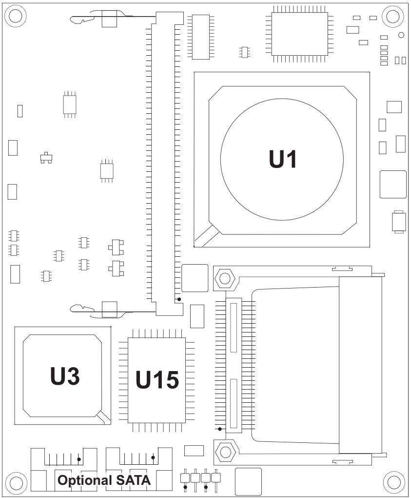
Table 2-1 lists the major ICs, including a brief description of each, on the ETX 620. Figures 2-4 and 2-5 show the locations of the ICs.

Table 2-1. Major Components Descriptions and Functions

<table><tr><td>Chip Type</td><td>Mfg.</td><td>Model</td><td>Description</td><td>Function</td></tr><tr><td>CPU (U1) [See Figure 2-4.]</td><td>AMD</td><td>Geode LX800</td><td>500 MHz CPU</td><td>Memory and Video</td></tr><tr><td>I/O Hub (U3) [See Figure 2-4.]</td><td>AMD</td><td>CS5536</td><td>Southbridge functions (provides some of standard I/O functions)</td><td>I/O Functions</td></tr><tr><td>Super I/O (U15) [See Figure 2-4.]</td><td>Winbond Electronics, Corp.</td><td>W83627HG</td><td>Super I/O controller (provides remaining standard I/O functions)</td><td>I/O Functions</td></tr><tr><td>Ethernet Controller (U9) [See Figure 2-5 on page 10]</td><td>Intel</td><td>82551QM</td><td>Ethernet chip (provides one 10/100BaseT based network channel)</td><td>Ethernet functions</td></tr><tr><td>ISA Bridge (U11) [See Figure 2-5]</td><td>ITE</td><td>IT8888G-L</td><td>PCI-to-ISA bridge conversion</td><td>ISA Bus</td></tr><tr><td>SATA Controller (U12 - optional) [See Figure 2-5]</td><td>VIA</td><td>VT6421L</td><td>High speed serial signals for internal mass storage devices</td><td>Serial ATA</td></tr><tr><td>Audio (U14) [See Figure 2-5]</td><td>Realtek</td><td>ALC203-LF</td><td>Audio &#x27;97 CODEC for audio In/Out signals</td><td>Audio In/Out</td></tr><tr><td>LVDS Transmitter (U19 - optional) [See Figure 2-5]</td><td>National/Fairchild</td><td>DS90CF383B</td><td>RGB to LVDS conversion</td><td>LCD Video</td></tr></table>

![U1\nU3 U15\nOptional SATA](.5001839a-a-etx620-refman/eb6a628c086b4e7a4ae7db6c0700d1a8716c011ae65a2a847880ca563e91903c.jpg)

Figure 2-4. Component Location (Top View)
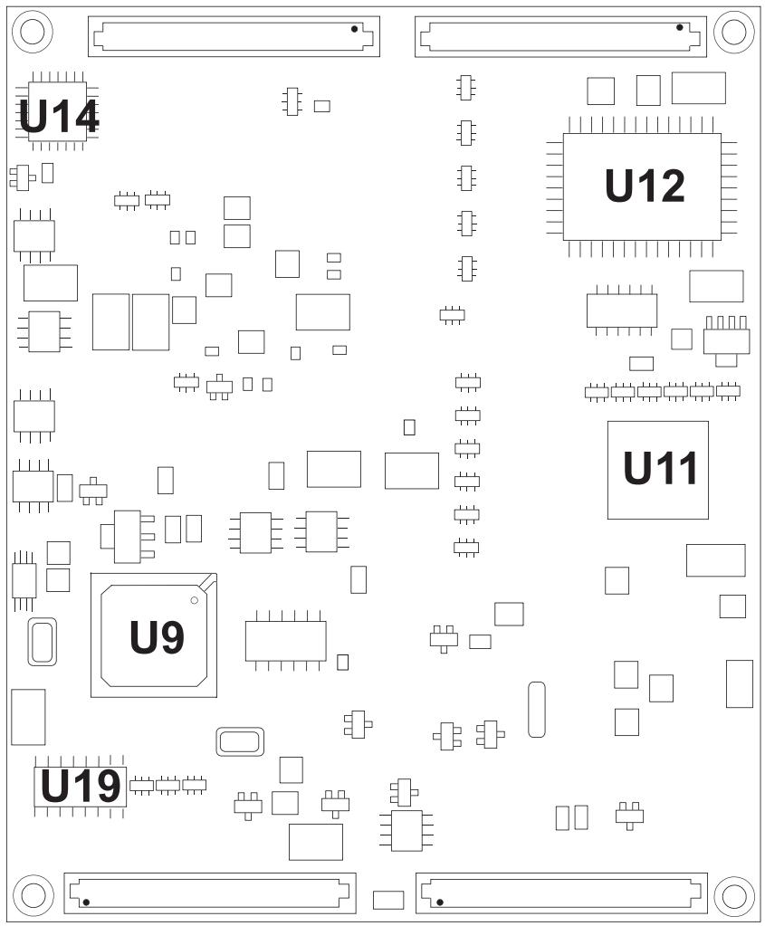
![U14\nU12\nU11\nU9\nU19](.5001839a-a-etx620-refman/e847a1554278e44e75180a892064f2c1678ec95b951b70848115e746cd140b4e.jpg)

Figure 2-5. Component Locations (Bottom View)

# Connector Definitions

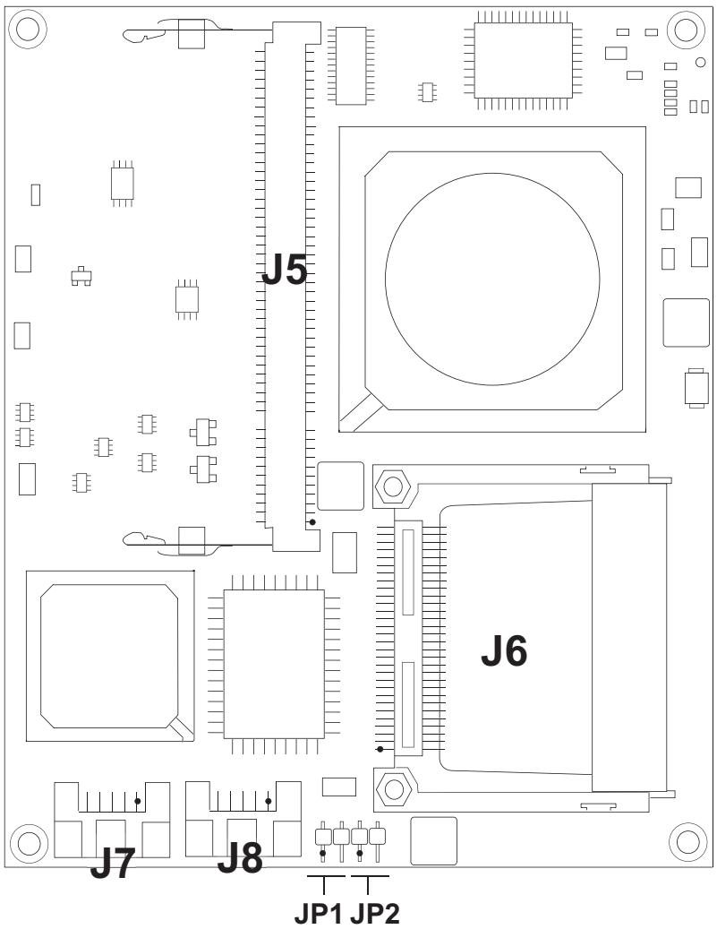
Table 2-2 describes the connectors shown in Figures 2-6 and 2-7. All I/O connectors use 0.100" pin (2.54mm) spacing unless otherwise indicated.

Table 2-2. Connector Descriptions

<table><tr><td>Jack #</td><td>Name</td><td>Description</td></tr><tr><td>J1</td><td>ETX X1 (on back of the board; see Figure 2-7 on page 12.)</td><td>Standard 100-pin, 0.6 mm Hirose connector for PCI, Audio, and USB signals</td></tr><tr><td>J2</td><td>ETX X2 (on back of the board; see Figure 2-7.)</td><td>Standard 100-pin, 0.6 mm Hirose connector for ISA signals</td></tr><tr><td>J3</td><td>ETX X3 (on back of the board; see Figure 2-7.)</td><td>Standard 100-pin, 0.6 mm Hirose connector for video, serial, keyboard and mouse, IrDA, parallel/floppy drive signals</td></tr><tr><td>J4</td><td>ETX X4 (on back of the board; see Figure 2-7.)</td><td>Standard 100-pin, 0.6 mm Hirose connector for IDE, Ethernet, and miscellaneous interface signals</td></tr><tr><td>J5</td><td>SODIMM</td><td>Standard un-buffered 200-pin socket for DDR memory</td></tr><tr><td>J6</td><td>CompactFlash</td><td>Standard 50-pin socket for Type II CompactFlash cards</td></tr><tr><td>J7</td><td>SATA1 (Optional)</td><td>Standard 7-pin, 1.27 mm connector for serial ATA signals</td></tr><tr><td>J8</td><td>SATA2 (Optional)</td><td>Standard 7-pin, 1.27 mm connector for serial ATA signals</td></tr></table>

![J5\nJ6\nJ7 J8\nJP1 JP2](.5001839a-a-etx620-refman/47a91fbad05bed7d697e7168b0841707ab56d060811550623c98546979d068dd.jpg)

Figure 2-6. Connector Locations (Top View)

NOTE Pin-1 is shown as a black pin (square or round) in all connectors and jumpers in all illustrations.
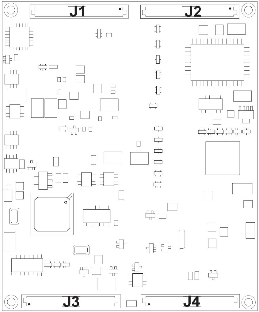
![J1\nJ2\nJ3\nJ4](.5001839a-a-etx620-refman/18146d23c9ed6687503a70681da215a98b2a7ff54c960b51e9356d058d229324.jpg)

Figure 2-7. Connector Locations (Bottom View)

# Jumper Definitions

Table 2-3 describes the jumpers shown in Figure 2-6 on page 11.

Table 2-3. Jumper Settings

<table><tr><td>Jumper #</td><td>Installed</td><td>Removed/Installed</td></tr><tr><td>JP1 – AT power</td><td>Enable Power Button (pins 1-2)</td><td>Disable Power Button (Removed)Default</td></tr><tr><td>JP2 – Compact Flash Master/Slave Select</td><td>Master (pins 1-2)</td><td>Slave (Removed) Default</td></tr></table>

NOTE Only the jumpers listed above are populated on the board. Jumpers or shunts use 2mm spacing. A jumper that is removed may be placed on one of the jumper pins for safe keeping.

# Specifications

# Physical Specifications

Table 2-4 gives the physical dimensions of the board.
Table 2-4. Weight and Footprint Dimensions

<table><tr><td>Item</td><td>Dimension</td><td rowspan="6">NOTE</td><td rowspan="6">Overall height is measured from the upper board surface to the highest permanent component (CompactFlash socket) on the upper board surface. This measurement does not include the various heatsinks on the board.</td></tr><tr><td>Weight</td><td>0.10kg (0.20 lb)</td></tr><tr><td>Height (overall)</td><td>6.35mm (0.25&quot;)</td></tr><tr><td>Width</td><td>95.25mm (3.75&quot;)</td></tr><tr><td>Length</td><td>114.3mm (4.5&quot;)</td></tr><tr><td>Thickness</td><td>2.36mm (0.093&quot;)</td></tr></table>

# Environmental Specifications

Table 2-5 provides the most efficient operating and storage condition ranges required for this board.
Table 2-5. Environmental Requirements

<table><tr><td></td><td>Parameter</td><td>500MHz Geode LX 800 Conditions</td></tr><tr><td rowspan="3">Temperature</td><td>Operating</td><td>-20° to +70°C (-4° to +158°F)</td></tr><tr><td>Extended (Optional)</td><td>-40° to +85°C (-40° to +185°F)</td></tr><tr><td>Storage</td><td>-55° to +85°C (-67° to +185°F)</td></tr><tr><td rowspan="2">Humidity</td><td>Operating</td><td>5% to 90% relative humidity, non-condensing</td></tr><tr><td>Non-operating</td><td>5% to 95% relative humidity, non-condensing</td></tr></table>

# Power Specifications

Tables 2-6 and 2-7 show the power requirements for the ETX 620.
Table 2-6. Power Supply Requirements (with SATA option)

<table><tr><td>Parameter</td><td>500MHz Geode LX 800 Characteristics w/LVDS</td><td>500MHz Geode LX 800 Characteristics w/TTL</td></tr><tr><td>Input Type</td><td>Regulated DC voltages</td><td>Regulated DC voltages</td></tr><tr><td>In-rush Current (Typical)</td><td>16.12A (80.60W)</td><td>16.12A (80.60W)</td></tr><tr><td>Idle Power (Typical)</td><td>2.00A (9.98W)</td><td>1.71A (8.54W)</td></tr><tr><td>BIT* Current (Typical)</td><td>2.65A (13.24W)</td><td>2.49A (12.47W)</td></tr></table>

# Operating conditions:

In-rush operating configuration includes video, 512MB DDR RAM, and power.
Idle operating configuration includes the in-rush configuration as well as one IDE hard drive with Windows XP Pro, one on-board CompactFlash drive with 64MB CompactFlash, floppy, keyboard, and mouse.
\*BIT = Burn-In-Test. Operating configuration includes idle conditions as well as two serial loop-backs, one Ethernet connection, four USB CompactFlash readers with 64MB CompactFlash.

Table 2-7. Power Supply Requirements (without SATA option)

<table><tr><td>Parameter</td><td>500MHz Geode LX 800 Characteristics w/LVDS</td><td>500MHz Geode LX 800 Characteristics w/TTL</td></tr><tr><td>Input Type</td><td>Regulated DC voltages</td><td>Regulated DC voltages</td></tr><tr><td>In-rush Current (Typical)</td><td>14.64A (73.20W)</td><td>14.64A (73.20W)</td></tr><tr><td>Idle Power (Typical)</td><td>1.64A (8.21W)</td><td>1.67A (8.35W)</td></tr><tr><td>BIT* Current (Typical)</td><td>2.28A (11.41W)</td><td>2.25A (11.25W)</td></tr></table>

# Operating conditions:

In-rush operating configuration includes video, 512MB DDR RAM, and power.
Idle operating configuration includes the in-rush configuration as well as one IDE hard drive with Windows XP Pro, one on-board CompactFlash with 512MB CompactFlash, floppy, keyboard, and mouse.
\*BIT = Burn-In-Test. Operating configuration includes idle conditions as well as two serial loop-backs, one Ethernet connection, four USB CompactFlash readers with 64MB CompactFlash.

# Thermal/Cooling Requirements

The ETX 620 is designed to operate at the maximum speed of the 500 MHz CPU without heatsinks or fans. Ampro offers an optional cooling solution, if needed.

# Overview

This chapter discusses the chips and features of the ETX 620 in the following order:

Interrupt Channel Assignments
• Memory Map
• I/O Address Map
• PCI Bus Interface (J1)
♦ USB
Audio Interface
ISA Bus Interface (J2)
• Primary I/O Interface (J3)
♦ Floppy/Parallel Interface
Serial Port Interfaces
♦ Keyboard
♦ Mouse
♦ Infrared (IrDA)
♦ Video Interfaces (CRT and TTL or LVDS)

IDE and Auxiliary Interface (J4)

♦ Primary IDE Interface
Ethernet Interface
♦ Battery for Real Time Clock (RTC)
♦ Speaker
♦ Power Control and Management
+ SMBus

. Miscellaneous

♦ Oops! Jumper (BIOS recovery)
♦ Remote Access (Serial Console)
Watchdog timer (WDT)
♦ Power Interface (including ACPI)

# NOTE

Ampro Computers, Inc. only supports the features/options tested and listed in this manual. The main integrated circuits (chips) used in the ETX 620 may provide more features or options than are listed for the ETX 620, but some of these chip features/options are not supported on the board and will not function as specified in the chip documentation.

# Interrupt Channel Assignments (IRQs)

The interrupt channel assignments are listed in Table 3-1.

Table 3-1. Interrupt Channel (IRQs) Assignments (Typical)

<table><tr><td>Device vs IRQ No.</td><td>0</td><td>1</td><td>2</td><td>3</td><td>4</td><td>5</td><td>6</td><td>7</td><td>8</td><td>9</td><td>10</td><td>11</td><td>12</td><td>13</td><td>14</td><td>15</td></tr><tr><td>Timer</td><td>D</td><td></td><td></td><td></td><td></td><td></td><td></td><td></td><td></td><td></td><td></td><td></td><td></td><td></td><td></td><td></td></tr><tr><td>Keyboard</td><td></td><td>D</td><td></td><td></td><td></td><td></td><td></td><td></td><td></td><td></td><td></td><td></td><td></td><td></td><td></td><td></td></tr><tr><td>Secondary Cascade</td><td></td><td></td><td>D</td><td></td><td></td><td></td><td></td><td></td><td></td><td></td><td></td><td></td><td></td><td></td><td></td><td></td></tr><tr><td>COM1</td><td></td><td></td><td></td><td>O</td><td>D</td><td></td><td></td><td></td><td></td><td></td><td></td><td></td><td></td><td></td><td></td><td></td></tr><tr><td>COM2</td><td></td><td></td><td></td><td>D</td><td>O</td><td></td><td></td><td></td><td></td><td></td><td></td><td></td><td></td><td></td><td></td><td></td></tr><tr><td>Floppy</td><td></td><td></td><td></td><td></td><td></td><td></td><td>D</td><td></td><td></td><td></td><td></td><td></td><td></td><td></td><td></td><td></td></tr><tr><td>Parallel</td><td></td><td></td><td></td><td></td><td></td><td>O</td><td></td><td>D</td><td></td><td></td><td></td><td></td><td></td><td></td><td></td><td></td></tr><tr><td>RTC</td><td></td><td></td><td></td><td></td><td></td><td></td><td></td><td></td><td>D</td><td></td><td></td><td></td><td></td><td></td><td></td><td></td></tr><tr><td>IDE Primary</td><td></td><td></td><td></td><td></td><td></td><td></td><td></td><td></td><td></td><td></td><td></td><td></td><td></td><td></td><td>D</td><td>O</td></tr><tr><td>Math Coprocessor</td><td></td><td></td><td></td><td></td><td></td><td></td><td></td><td></td><td></td><td></td><td></td><td></td><td></td><td>D</td><td></td><td></td></tr><tr><td>PS/2 Mouse</td><td></td><td></td><td></td><td></td><td></td><td></td><td></td><td></td><td></td><td></td><td></td><td></td><td>D</td><td></td><td></td><td></td></tr><tr><td>AC’97 CODEC</td><td></td><td></td><td></td><td></td><td></td><td>D</td><td></td><td></td><td></td><td></td><td></td><td></td><td></td><td></td><td></td><td></td></tr><tr><td>PCI SLOT - 1</td><td colspan="16">Automatically Assigned or User selectable</td></tr><tr><td>PCI SLOT - 2</td><td colspan="16">Automatically Assigned or User selectable</td></tr><tr><td>PCI SLOT - 3</td><td colspan="16">Automatically Assigned or User selectable</td></tr><tr><td>PCI SLOT - 4</td><td colspan="16">Automatically Assigned or User selectable</td></tr><tr><td>USB</td><td colspan="16">Automatically Assigned</td></tr><tr><td>VGA</td><td colspan="16">Automatically Assigned</td></tr><tr><td>Ethernet</td><td colspan="16">Automatically Assigned</td></tr></table>

Legend: D = Default, O = Optional

NOTE The IRQs for the Ethernet, Video, USB, and PCI are automatically assigned by the BIOS Plug and Play logic. Local IRQs assigned during initialization can not be used by external devices.

# Memory Map

Table 3-2 provides the common PC/AT memory allocations. BIOS uses memory below 000500h.

Table 3-2. Memory Map

<table><tr><td colspan="2">Base Address</td><td>Function</td></tr><tr><td>00000000h</td><td>- 0009FFFFh</td><td>Conventional Memory</td></tr><tr><td>000A0000h</td><td>- 000AFFFFh</td><td>Graphics Memory</td></tr><tr><td>000B0000h</td><td>- 000B7FFFh</td><td>Mono Text Memory</td></tr><tr><td>000B8020h</td><td>- 000BFFFFh</td><td>Color Text Memory</td></tr><tr><td>000C0000h</td><td>- 000C7FFFh</td><td>Standard Video BIOS</td></tr><tr><td>000E0000h</td><td>- 000FFFFFFh</td><td>System BIOS Area (Storage and RAM Shadowing)</td></tr><tr><td>00100000h -</td><td>04000000h</td><td>Extended Memory (If onboard VGA is enabled, then the amount of memory assigned is subtracted from extended memory)</td></tr><tr><td>FFF80200h -</td><td>FFFFFFFFh</td><td>System Flash</td></tr></table>

# I/O Address Map

Table 3-3 provides the I/O address map.

Table 3-3. I/O Address Map

<table><tr><td>Address (hex)</td><td>Subsystem</td></tr><tr><td>000-00F</td><td>Primary DMA Controller</td></tr><tr><td>020-021</td><td>Master Interrupt Controller</td></tr><tr><td>040-043</td><td>Programmable Interrupt Timer (Clock/Timer)</td></tr><tr><td>060-06F</td><td>Keyboard Controller</td></tr><tr><td>070-07F</td><td>CMOS RAM, NMI Mask Reg, RT Clock</td></tr><tr><td>080-09F</td><td>DMA Page Registers</td></tr><tr><td>102</td><td>Video subsystem register</td></tr><tr><td>0A0-0BF</td><td>Slave Interrupt Controller</td></tr><tr><td>0C0-0DF</td><td>Slave DMA Controller #2</td></tr><tr><td>0F0-0FF</td><td>Math Coprocessor</td></tr><tr><td>1F0-1F8</td><td>Primary IDE Hard Disk Controller</td></tr><tr><td>201</td><td>Watchdog Timer (WDT)</td></tr><tr><td>278-27F</td><td>Parallel Printer</td></tr><tr><td>2F8-2FF</td><td>Serial Port 2 (COM2)</td></tr><tr><td>378-37F</td><td>Parallel Port (Standard and EPP)</td></tr><tr><td>3C0-3DF</td><td>VGA</td></tr><tr><td>3F0-3F7</td><td>Floppy Disk Controller</td></tr><tr><td>3F8-3FF</td><td>Serial Port 1 (COM1)</td></tr><tr><td>778-77A</td><td>Parallel Port (ECP Extensions) (Port 378+400)</td></tr><tr><td>A79</td><td>ISA PnP Ports</td></tr><tr><td>CF8-CFF</td><td>PCI bus Configuration Address and Data</td></tr></table>

# X1 PCI Bus Interface

The J1, 100-pin connector is used for the PCI bus, USB ports, and Audio (AC’97) interface connections. This section briefly describes each of these features.

# PCI Bus

The CPU (Geode LX800) integrates a PCI arbiter that supports up to four external PCI masters.

This interface carries all of the appropriate PCI signals
Bus operates at clock speeds up to 33 MHz.
PCI 2.2 Compliant, 32-bit +3.3V PCI interface with +5V tolerant inputs

# Universal Serial Bus (USB)

The ETX 620 module supports up to four USB ports on the baseboard and the supported features are listed below.

USB v2.0 and backwards compatible to Universal OHCI v1.1
Two root USB hubs and 4 USB ports
Supports USB boot of floppy disk drives, hard disk drives, CD-ROMs, or other USB boot devices.
Integrated physical layer transceivers
Over-current detection status on USB ports 1 and 2

# Serial Interrupt Request

This SERIRQ signal is connected to serial request input on the I/O Hub (CS5536) for the alternative ISA/ PCI interrupts. If this feature is utilized, then DMA2 (DAck2 and DRQ2) will be supported by ETX 620 module. The ETX 620 SERIRQ pin (pin 21) must be connected to the baseboard to use the ISA bus on the baseboard.

Table 3-4. Simplified Serial Interrupt Request Description (J1)

<table><tr><td>J1 Pin #</td><td>Signal</td><td>Description</td></tr><tr><td>21</td><td>SERIRQ</td><td>Serial Interrupt Request – This pin is used to support the serial interrupt protocol.</td></tr></table>

# Audio Interface

The RealTek Audio CODEC (ALC203) on the ETX 620 supports the AC’97 audio standard and the supported features listed below.

I/O Hub (CS5536) supports the onboard CODEC (ALC203)
AC’97 Rev 2.3 compliant
Supports audio amplifier on baseboard
PC-Beep passthrough to Line Out while reset is held active low
True Line Level Output with volume control independent of Line Out
Digital 3V and 5V compliant

# X2 ISA Bus Interface

The J2, 100-pin connector is used for standard ISA interface connections. The CPU does not directly support an ISA expansion interface. A provision for ISA bus capabilities is provided in this connector through an onboard PCI-to-ISA bridge.

# X3 Primary I/O Interface

The J3, 100-pin connector is used for Floppy or Printer (LPT1) interface, Serial interfaces (COM1 and COM2), Mouse and Keyboard interfaces, Infrared (IrDA) interface, and the video interfaces for standard CRT and TTL or LVDS video. This section briefly describes each of these features.

# Floppy Interface

The Floppy interface shares signal lines with the Parallel interface and is provided by the Super I/O chip (W83627HG). The BIOS settings determine which one is operational. This type of connector can be located on the custom baseboard if desired.

Supports two floppy drives
16 bytes of FIFO with data rates up to 1 Mbps

# Parallel Interface

Parallel interface supports standard parallel, Bi-directional, ECP and EPP protocols. The Super I/O chip (W83627HG) provides the parallel interface signals, which are shared with the floppy drive interface.

The Parallel interface shares signal lines with the Floppy interface and the BIOS settings determine which one is operational.
Supports Standard Printer Port (SPP), Enhanced Parallel Port (EPP) and Enhanced Capabilities Port (ECP)
• A DB25 connector can be located on the custom baseboard if desired.

# Serial Ports 1 and 2

The Super I/O chip (W83627HG) provides the circuitry for two serial port UARTs with TTL compatible signals. The signals for serial ports 1 and 2 are provided to the baseboard through connector J3. However, the baseboard must provide the serial transceivers to make use of this feature. The serial port features are:

Two individual 16550-compatible UARTs
Programmable word length, stop bits and parity
16-bit programmable baud rate generator and Interrupt generator
Loop-back mode
Two individual 16-bit FIFOs
DB9 connectors can be designed onto the custom baseboard, as the application requires.

# Infrared (IrDA) Port

The Infrared Data Association (IrDA) port provides two-way wireless communications port signals using infrared as a transmission medium at the basic level. However, the custom baseboard must provide the infrared (IrDA) transceiver to implement this feature. There are two basic infrared implementations provided; the Hewlett-Packard Serial Infrared (HPSIR) and the Amplitude Shift Keyed Infrared (ASKIR) methods. HPSIR is a serial implementation of infrared developed by Hewlett-Packard. The IrDA (HPSIR and ASKIR) signals share Serial Port 2 with the modem and RS232 functions on the port. This port can be enabled/disabled and configured for HPSIR or ASKIR signals in the BIOS Setup Utility. Refer to Advanced Settings in Chapter 4, BIOS Setup Utility for more information.

The HPSIR method allows serial communication at baud rates up to 115 k baud. Each word is sent serially beginning with a zero value start bit. A zero is sent when a single infrared pulse is sent at the beginning of the serial bit time. A one is sent when no infrared pulse is sent during the bit time.

The Amplitude Shift Keyed infrared (ASKIR) allows serial communication at baud rates up to 19.2 k baud. Each word is sent serially beginning with a zero value start bit. A zero is sent when a 500 kHz waveform is sent for the duration of the serial bit time. A one is sent when no transmission is sent during the serial bit time.

Both of these methods require an understanding of the timing diagrams provided in the Super I/O controller (W83627HG) specifications available from the manufacture’s web site and referenced earlier in this manual.

For more information, refer to the Nuvoton Technology, Corp. W83627HG databook and the Infrared Data Association web site at http://www.irda.org.

NOTE For infrared applications not covered in this brief description, refer to the W83627HG chip specifications by Nuvoton Technology, Corp.

# PS/2 Keyboard

The signal lines for a PS/2 keyboard are provided through the J3 connector from the Super I/O chip (W83627HG).

# PS/2 Mouse

The signal lines for a PS/2 mouse are provided through the J3 connector from the Super I/O chip (W83627HG).

# CRT Interface

Graphic controller is integrated in the CPU (Geode LX800).
Maximum resolution for CRT output is 1600x1200x32 with full use of 64 MB Unified Memory Architecture (UMA).

# LVDS Interface

The CPU provides RGB signals which, on certain versions of the ETX 620, are converted to LVDS through an LVDS transmitter. This output is independent of other panel interfaces. The LVDS interface will support 1 or 2 channels. A single channel interface uses the Y[2:0]+, Y[2:0]-, and YCLK+ and YCLK- outputs. The second LVDS interface is assigned the Z[2:0]+, Z[2:0]-, and ZCLK+ and ZCLK- outputs.

Note: The shaded area denotes power or ground.
Table 3-5. Simplified LVDS Interface Pin/Signal Descriptions (J3)

<table><tr><td>J3 Pin #</td><td>Signal</td><td>Description</td><td>Line</td><td>Channel</td></tr><tr><td></td><td>GND</td><td>Ground</td><td>NA</td><td>NA</td></tr><tr><td>37</td><td>LCDDO0</td><td>Data Negative Output</td><td rowspan="2">0</td><td rowspan="10">Channel 1</td></tr><tr><td>35</td><td>LCDDO1</td><td>Data Positive Output</td></tr><tr><td>38</td><td>LCDDO2</td><td>Data Negative Output</td><td rowspan="2">1</td></tr><tr><td>36</td><td>LCDDO3</td><td>Data Positive Output</td></tr><tr><td>29</td><td>LCDDO4</td><td>Data Negative Output</td><td rowspan="2">2</td></tr><tr><td>31</td><td>LCDDO5</td><td>Data Positive Output</td></tr><tr><td>32</td><td>LCDDO6</td><td>Clock Negative Output</td><td rowspan="2">Clock</td></tr><tr><td>30</td><td>LCDDO7</td><td>Clock Positive Output</td></tr><tr><td>23</td><td>LCDDO8</td><td>Data Negative Output</td><td rowspan="2">3</td></tr><tr><td>25</td><td>LCDDO9</td><td>Data Positive Output</td></tr><tr><td>26</td><td>LCDDO10</td><td>Data Negative Output</td><td rowspan="2">0</td><td rowspan="10">Channel 2</td></tr><tr><td>24</td><td>LCDDO11</td><td>Data Positive Output</td></tr><tr><td>19</td><td>LCDDO12</td><td>Data Negative Output</td><td rowspan="2">1</td></tr><tr><td>17</td><td>LCDDO13</td><td>Data Positive Output</td></tr><tr><td>20</td><td>LCDDO14</td><td>Data Negative Output</td><td rowspan="2">2</td></tr><tr><td>18</td><td>LCDDO15</td><td>Data Positive Output</td></tr><tr><td>11</td><td>LCDDO16</td><td>Clock Negative Output</td><td rowspan="2">Clock</td></tr><tr><td>13</td><td>LCDDO17</td><td>Clock Positive Output</td></tr><tr><td>12</td><td>LCDDO18</td><td>Data Negative Output</td><td rowspan="2">3</td></tr><tr><td>14</td><td>LCDDO19</td><td>Data Positive Output</td></tr><tr><td>41</td><td>JILI_DAT</td><td colspan="3">Flat Panel  $I^{2}C$  Data –  $I^{2}C$  data interface to flat panel parameter EEPROM.</td></tr><tr><td>43</td><td>JILI_CLK</td><td colspan="3">Flat Panel  $I^{2}C$  Clock –  $I^{2}C$  clock interface to flat panel parameter EEPROM.</td></tr><tr><td>44</td><td>BLON*</td><td colspan="3">Backlight On – Control signal for external flat panel backlight power.</td></tr><tr><td>45</td><td>BIASON</td><td colspan="3">BIAS ON – Flat panel contrast voltage control.</td></tr><tr><td>46</td><td>DIGON</td><td colspan="3">Digital Power-On – Digital flat panel power on control.</td></tr></table>

NOTE The necessary voltages to drive a flat panel are not supplied through the J3 connector on the ETX 620 module. The required drive voltages for the flat panel must be designed into the customer’s baseboard and supplied from the ATX or AT power supply to provide drive voltages for the LVDS connector to the flat panel.

# TTL Flat Panel Interface

The TFT controller converts RGB output of a Video Mixer block to the digital output suitable for driving a TTL flat panel. Table 3-6 describes the signals of the TTL interface.

Table 3-6. Simplified TTL Flat Panel Interface Pin/Signal Descriptions (J3)

<table><tr><td>Pin #</td><td>Signal</td><td>Description</td></tr><tr><td>11</td><td>DRGB6</td><td>Flat Panel Data Output, B6</td></tr><tr><td>12</td><td>CLK_DOT</td><td>Clock</td></tr><tr><td>13</td><td>DRGB7</td><td>Flat Panel Data Output, B7</td></tr><tr><td>14</td><td>LCD_EN</td><td>LCD Enable</td></tr><tr><td>17</td><td>DRGB3</td><td>Flat Panel Data Output, B3</td></tr><tr><td>18</td><td>DRGB5</td><td>Flat Panel Data Output, B5</td></tr><tr><td>19</td><td>DRGB2</td><td>Flat Panel Data Output, B2</td></tr><tr><td>20</td><td>DRGB4</td><td>Flat Panel Data Output, B4</td></tr><tr><td>23</td><td>DRGB12</td><td>Flat Panel Data Output, G4</td></tr><tr><td>24</td><td>DRGB15</td><td>Flat Panel Data Output, G7</td></tr><tr><td>25</td><td>DRGB13</td><td>Flat Panel Data Output, G5</td></tr><tr><td>26</td><td>DRGB14</td><td>Flat Panel Data Output, G6</td></tr><tr><td>29</td><td>DRGB22</td><td>Flat Panel Data Output, R6</td></tr><tr><td>30</td><td>DRGB11</td><td>Flat Panel Data Output, G3</td></tr><tr><td>31</td><td>DRGB23</td><td>Flat Panel Data Output, R7</td></tr><tr><td>32</td><td>DRGB10</td><td>Flat Panel Data Output, G2</td></tr><tr><td>35</td><td>DRGB19</td><td>Flat Panel Data Output, R3</td></tr><tr><td>36</td><td>DRGB21</td><td>Flat Panel Data Output, R5</td></tr><tr><td>37</td><td>DRGB18</td><td>Flat Panel Data Output, R2</td></tr><tr><td>38</td><td>DRGB20</td><td>Flat Panel Data Output, R4</td></tr></table>

# X4 IDE and Auxiliary Interface

The J4 connector has 100 pins and is used for IDE port, Ethernet port, RTC/Battery, speaker, power management, SMBus, and miscellaneous power interface signals. This section describes each of these features.

# IDE Port

Supports one EIDE channel
Supports EIDE Ultra DMA 33/66/100 in Master Mode
Supports ATAPI compliant devices including DVD devices
Supports PIO IDE transfers up to 14 Mbytes/sec
Supports IDE Bus Master transfers up to 100 Mbytes/sec

The IDE channel can be routed to the IDE connector or a CompactFlash socket on a custom baseboard per the application requirements.

# Ethernet Port Interface

The Ethernet solution is provided by an Intel 82551QM Fast Ethernet PCI controller chip, which consists of both the Media Access Controller (MAC) and the physical layer (PHY) combined into a single component solution. The 82551QM is a 32-bit PCI controller that features enhanced scatter-gather bus mastering capabilities, which enables the 82551QM to perform high-speed data transfers over the PCI bus. The 82551QM bus master capabilities enable the component to process high-level commands and perform multiple operations, thereby off-loading communication tasks from the system CPU.

Routed to J4 connector
Low power 3.3 V device
Backward software compatible to the 82559, 82558, and 82557
Chained memory structure
Supports full duplex or half-duplex operation
Supports full duplex operation at 10 Mbps and 100 Mbps
• Supports half-duplex mode with enhanced performance by a proprietary collision reduction mechanism
Provides IEEE 802.3 10BaseT/100BaseT compatible physical layer
Supports data transmission with minimum interframe spacing (IFS).
Supports IEEE 802.3u Auto-Negotiation
• Provides 3 KB transmit and 3 KB receive FIFOs (helps prevent data underflow and overflow)
Provides IEEE 802.3x 100BASE-TX flow control

• Improved dynamic transmit chaining with multiple priorities transmit queues
Supports an Ethernet port RJ-45 connector and the magnetics on the baseboard only

# Power Control Signals

The ETX 620 supports various power control signals provided through the baseboard to control the ETX 620 and the power supply.

The Power Good input signal (PWGIN) is provided from an external input typically from the external power supply (ATX) to the baseboard. This signal is typically an active-high input to the ETX baseboard and indicates to the ETX module it can begin the boot process. This Power Good signal can also be used as an active-low reset input to the ETX module.
The Power Suspend signal (5V\_SB) must be provided through the power supply interface for standby operation, typically an ATX power supply. The power supply must provide a 5 volt 100 mA stand-by power source for this function to be available.
The Power On signal (PS\_ON) is provided by the ETX module to the PS\_ON input of an ATX power supply allowing it to switch to main output power from a standby state. This signal is used in conjunction with the 5V\_SB supplied to the ETX module from the ATX power supply.
The Power Button Input signal (PWRBTN\*) provides a ground temporally through a momentarycontact switch or through an open collector driver to the ATX power supply. This signal is used in conjunction with the PS\_ON and the 5V\_SB signals from the ATX power supply to activate the power control function of the power supply.
A voltage monitor on the ETX 620 tracks the VCC voltage (+5 volts) state by monitoring the +3.3V generated on the ETX module. When the +3.3V drops below 3.0V or the Reset Button signal goes low, the voltage monitor sends a reset pulse to the CPU (Geode LX800) and the I/O Hub (CS5536).

# Power Management Signals

The ETX 620 supports various power management signals described in the following list.

The External System Management Interrupt (EXTSMI) signal is routed to the baseboard through J4 to allow external circuitry to initiate an SMI for the EXT module.
The Resume Reset input (RSMRST\*) signal to the EXT module may be driven low by external control circuitry to reset the power management logic on the ETX module.
The System Management Bus Alert input (SMBALRT\*) signal is used by SMBus devices to indicate an event on the SMBus to the EXT module.
The Battery Low input (BATLOW\*) signal is used by external voltage monitoring circuitry to indicate the system battery is low to the ETX module.

# Speaker

The signal lines for a speaker port with 0.1-watt drive are provided through J4 connector to the baseboard where the speaker must be located.

The I/O Hub (CS5536, Southbridge) provides the speaker output signal, but the output drive circuit must be implemented on the baseboard.

# Real Time Clock (RTC)/Battery

The ETX 620 supports a Real Time Clock (RTC) and CMOS RAM for the BIOS Setup Utility. The RTC and 256 byte of CMOS RAM are included inside the I/O Hub (CS5536). The RTC and CMOS are backed up through the BAT pin on J4 with a Lithium Battery located on the baseboard. If the battery is not present, the BIOS has a battery-free boot option to complete the boot process.

# SMBus

The I/O Hub (CS5536) contains an integrated SMBus controller with both a host and slave SMBus port; but the host cannot access the slave internally. The slave port allows an external master access to the I/O Hub through the J4 connector. The master contained in the I/O Hub is used to communicate with the SEEP, SDRAM EPROM, and the clock generator. Table 3-7 lists the addresses for these devices with the components and corresponding binary addresses of the SMBus.

Table 3-7. SMBus Reserved Addresses

<table><tr><td>Matrix Component</td><td>Address Binary</td></tr><tr><td>Configuration SEEP</td><td> $1010,010x_b$ </td></tr><tr><td>SDRAM EPROM</td><td> $1010,000x_b$ </td></tr><tr><td>Clock Generator (ICS950811)</td><td> $1101,001x_b$ </td></tr><tr><td>I/O Hub (82801DBM)</td><td> $0000,000x_b$  (default) Programmable</td></tr></table>

# Miscellaneous

# Oops! Jumper (BIOS Recovery)

The Oops! jumper is provided in the event the BIOS settings you have selected prevent you from booting the system. By using the Oops! jumper you can prevent the current BIOS settings in the Flash memory from being loaded, forcing the use of the default settings. Connect the DTR pin to the RI pin on serial port 1 (COM 1) on the baseboard prior to boot up to prevent the present BIOS settings from loading. After booting with the Oops! jumper in place, remove the Oops! jumper from the baseboard connector and go into the BIOS Setup Utility. Change the desired BIOS settings, or select the default settings, and save changes before rebooting the system.

To convert a standard DB9 connector to a Oops! jumper for use on the custom baseboard, short together the DTR (4) and RI (9) pins on the rear of the connector as shown in Figure 3-1 on the Serial Port 1 DB9 connector.

![Standard DB9 Serial\nPort Connector (Female)\nRear View\n1 2 3 4 5\n6 7 8 9\nETX620_Oopsjump](.5001839a-a-etx620-refman/36a2bcd63e9c148477a893734d93d67c23a90c82faa7bd4ce1a3d42c6916d9ef.jpg)

Figure 3-1. Oops! Jumper Connection

# Serial Console (Remote Access)

The BIOS Setup Utility supports the serial console (or console redirection) feature, but refers to it as Remote Access. This I/O function can be accessed by an ANSI-compatible serial terminal, or the equivalent terminal emulation software running on another system. This can be very useful when setting up the BIOS on a production line for systems that are not connected to a keyboard and display (sometimes referred to as a headless system).

# Serial Console Setup

The serial console feature is implemented by connecting a standard null modem cable or a modified serial cable (or “Hot Cable”) between one of the serial ports, such as Serial 1 or Serial 2, and the serial terminal or a PC with communications software. The BIOS Setup Utility controls the serial console settings for the ETX 620. Refer to Entering BIOS Setup Utility (Remote Access/Serial Console) and Advanced settings, in Chapter 4, BIOS Setup Utility for the Remote Access option to set the serial terminal, or PC with communications software.

# Hot (Serial) Cable

To convert a standard serial cable to a Hot Cable for use on the custom baseboard, two pins must be shorted together at the Serial port DB9 connector. Short together the RTS (7) and RI (9) pins on Serial port DB9 connector as shown in Figure 3-2.

![Standard DB9 Serial\nPort Connector (Female)\nRear View\n1 2 3 4 5\n6 7 8 9\nETX620_HotCable](.5001839a-a-etx620-refman/7448fbd9035971c72fe8cb3db52705608f4e67829edb40fd209f11d76f5b68c9.jpg)

Figure 3-2. Hot Cable Jumper

# Watchdog Timer (WDT)

The watchdog timer (WDT) restarts the system if an error or mishap occurs, allowing the system to recover from the mishap, even though the error condition may still exist. Possible problems include failure to boot properly, loss of control by the application software, failure of an interface device, unexpected conditions on the bus, or other hardware or software malfunctions.

The WDT (watchdog timer) can be used both during the boot process and during normal system operation.

During the Boot process – If the operating system fails to boot in the time interval set in the BIOS, the system will reset.
The watchdog timer (WDT) is enabled and configured in the Boot settings screen of the BIOS Setup Utility. Set the WDT for a time-out interval in seconds, between 1 and 255, in one second increments. Ensure you allow enough time for the operating system to boot. The OS or application must tickle (reset) the WDT before the timer expires. This can be done by accessing the hardware directly or through a BIOS call.
During System Operation – An application can set up the WDT hardware through a BIOS call, or by accessing the hardware directly. Some Ampro Board Support Packages provide an API interface to the WDT. The application must tickle (reset) the WDT before the timer expires or the system will be reset. The BIOS implements interrupt 15 function 0C3h to manipulate the WDT.
Watchdog Code examples – Ampro will provide code examples on the ETX 620 Support Software DVD illustrating how to control the WDT in the final release.

# Power Interface

The ETX 620 draws its input voltage (+5V) through the four connectors (X1, X2, X3, X4) on the custom baseboard, which requires an external power supply, typically an ATX power supply or other power source as the application requires. The ETX 620 generates its own internal voltages onboard, including the CPU core voltages and requires the externally supplied +5 volts DC +/- 5%.

The –5V, –12V, +12V and +3.3V voltages used for the PCI and ISA buses and the LVDS video connector are supplied to the baseboard and ETX 620 module from the externally connected power supply, typically an ATX power supply.

# Power and Sleep States

The following information only applies if an ATX power supply is connected to the ETX baseboard where the ETX 620 is installed. If a non-ATX power supply is used, then the ETX 620 is only controlled by the Power-On/Off switch on the power supply and the various sleep states are not available. The ACPI sleep states are OS dependent and not available if your OS does not support power management based on the ACPI standard. The signals used for control of the ATX power supply and sleep states in general is described in more detail under Power Control Signals and Power Management Signals earlier in this chapter.

# Power-On Switch

The Power-On switch, on or connected to the ETX Baseboard, turns the ETX 620 and its attached power supply to a fully On condition, if you are using an ATX power supply and an OS that supports sleep states. If the operating system (OS) supports sleep states, the OS will turn off the ETX 620 and its power supply during the OS shut down process. Typically, the Power-On switch will also transition the ETX 620, the ETX baseboard, and its power supply between a fully powered on state and the various sleep states, including a fully powered off state. If the OS does not support sleep states, then the Power-On switch only turns power, On or Off, to the ETX 620 and its baseboard.

Typically, an OS that supports ACPI, also allows the Power-On switch to be configured through a user interface. The Power-On switch for the ETX 620 must be provided on, or connected to the baseboard.

# Sleep States (ACPI)

The ETX 620 supports the ACPI (Advanced Configuration and Power Interface) standard, which is a key component of certain Operating Systems’ (OS’s) power management. The supported features (sleep states) listed here are only available when an ACPI-compliant OS is used for the ETX 620, such as Windows 2000/ XP. The term “sleep” state refers to a low wake latency (reduced power consumption) state, which can be restarted (awakened) restoring full operation to the ETX 620.

In these various sleep states, the computer appears to be off, indicated by such things as no display on the attached monitor and no activity for the connected CD-ROM or hard drives. Normally, when a computer detects certain activity (i.e. power switch, mouse, keyboard, serial port, or certain types of LAN activity), it returns to a fully operational state.

NOTE Currently, the Power-On switch, Wake-on-Ring, Wake-on-LAN, Wake on RTX alarm, Wake on PME, and Keyboard/Mouse activity are the only activities that will wake the ETX 620 from a powered down state, such as Standby (S1), Suspend-to-RAM (S3), Hibernate (S4) and Power Off (S5). However, not all of the listed activities will wake each sleep state. Refer to the ETX 620 Software and Hardware Release Notes for more information.

The ETX 620 supports at least five ACPI power states, depending on the operating system used and its ability to manage sleep states. Typically, the Power-On switch is used to wake up from a sleep state, or transition from one state to another, but this is dependent on the operating system.

1st state is normal Power On (S0).

To go to a fully powered on state, the ETX 620 must either be powered Off (S5), or in a sleep state (S1 or S4), and then the Power-On switch is pressed for less than 4 seconds (default).
The ETX 620 can transition from this state (S0) to the various states described below, depending on the power management capability of the OS and how it is programmed.

2nd state is a standby state (S1).

In this state there are internal operations taking place, including the internal RTC (real time clock), contents of RAM, activity for the CPU, but the external peripherals, such as hard disk drives, CD-ROMs, and monitor are off. The ETX 620 appears to be on due to the Power-On LED.

Normally, to enter this sleep state, the ETX 620 must be fully powered on (S0) and the OS transitions the ETX 620 into this standby state (S1) under user control.
To exit this sleep state a wake up event, such as the Power-On switch, is used to wake up the ETX 620 and restore full operation, including the Power-On LED. Typically, pressing the Power-On switch for less than 4 seconds (default) will restore full operation.

3rd state is a suspend-to-RAM state (S3).

This sleep state stores your open files and programs in RAM before powering down. In this state there are no internal operations taking place, except for the internal RTC (real time clock) and low power level keeping the contents of RAM alive. This includes no activity for the CPU and external peripherals, such as hard disk drives or CD-ROMs. The ETX 620's Power-On LED is off, but the S3 Mode LED is turned on only when in S3 Mode. This state is only safe as long as you have power to your system. If power is lost to the ATX power supply or the battery fails, then the contents of RAM is lost, including any open applications and data files. This state is quicker than S4, but much more volatile.

Normally, to enter this sleep state, the ETX 620 must be fully powered on (S0) and the OS transitions the ETX 620 into this suspend-to-RAM (S3) state under user control.
To exit this sleep state a wake up event, such as the Power-On switch, is used to wake up the ETX 620 and restore full operation, including the Power-On LED, but the S3 Mode LED turns off. Typically, pressing the Power-On switch for less than 4 seconds (default) will restore full operation.

4th state is a hibernate or suspend-to-disk state (S4).

This condition stores the state of your system (open files and programs) on the hard disk drive before powering down. In this state there are no internal operations taking place, except for the internal RTC. This includes no activity for the RAM, CPU, and external peripherals, such as hard disk drives or CD-ROMs. The ETX 620 appears to be off, including the Power-On LED and the S3 Mode LED. Your system will take longer to wake-up in this sleep state than S3, but since your data is saved to the disk, it is more secure and should not be lost in the event of a power failure.

♦ To enter a hibernate or suspend-to-disk state, the ETX 620 must be fully powered on and the OS transitions the ETX 620 into this sleep state (S4) under user control.
To exit this sleep state a wake up even, such as the Power-On switch, is used to wake up the ETX 620 and restore full operation, including the Power-On LED. Typically, pressing the Power-On switch for less than 4 seconds (default) will restore full operation.

5th state is the normal power Off or shutdown (S5).

All activity stops except the internal clock, unless the power cord is removed from the power source.

To go to a fully powered down state, the ETX 620 must either be powered On, or in a sleep state, and then the Power-On switch is pressed for more than 4-to-6 seconds.
♦ To go to a fully powered up state, press the Power-On switch for less than 4 seconds (default) and full operation is restored.

The OS may provide additional programming features to change the activation time for each state, and to shutdown or transition the ETX 620 at certain times, depending on the way the OS interface is programmed. Refer to the OS vender’s documentation for power management conditions under the ACPI standard.

# Introduction

This section assumes the user is familiar with BIOS Setup and does not attempt to describe the inner workings of BIOS functions. Refer to the appropriate PC reference manuals for information about the onboard, ROM-BIOS software interface. If Ampro has added to or modified the standard functions, these functions will be described.

# Entering BIOS Setup (VGA Display)

To enter BIOS Setup using a VGA display for the ETX 620:

1. Turn on the VGA monitor and the power supply to the ETX 620.
2. Start Setup by pressing the [Del] key, when the following message appears on the boot screen.

Press DEL to run Setup

NOTE If the setting for Memory Test is set to Fast, you may not see this prompt appear on screen if the monitor is too slow to display it on start up. If this happens, press the &lt;Del&gt; key early in the boot sequence to enter BIOS Setup.

3. Use the &lt;Enter&gt; key to select the screen menus listed in the Opening BIOS screen.
4. Follow the instructions at the bottom of each screen to navigate through the selections and modify any settings.

# Entering BIOS Setup (Remote Access)

Once you set up the BIOS Utility for Remote Access (serial console or console redirection) in VGA mode, entering the BIOS in the remote access mode is very similar to the method used when entering the BIOS with a VGA display.

1. Turn on the power supply to the ETX 620 and access the BIOS Setup Utility in VGA mode.
2. Set the BIOS feature Remote Access to [Enabled] under the Advanced menu.
3. Accept the default options or make your own selections for the balance of the Remote Access fields and record your settings.
4. Ensure you select the type of remote serial terminal you will be using and record your selection.
5. Select Save Changes and Exit and then shut down the ETX 620.
6. Connect the remote serial terminal (or the PC with communications software) to the COM port you selected on the ETX 620 using a Hot Cable or a standard null-modem serial cable.
7. Turn on the remote serial terminal (or the PC with communications software) and set it to the settings you selected and recorded earlier in the BIOS Setup Utility.
COM1, 115200, 8 bits, 1 stop bit, no parity, no flow control, and [Always] for Redirection After BIOS POST are the default settings for the ETX 620.
8. Restore power to the ETX 620 and look for the screen prompt shown below.
Press ^C to run SETUP
9. Press the CTRL–C keys to enter Setup early in the boot sequence if Quick Boot is set to [Enabled]. If Quick Boot is set to [Enabled], you may never see the screen prompt.

10. Use the &lt;Enter&gt; key to select the screen menus listed in the Opening BIOS screen.

NOTE The serial console port is not hardware protected, and is not listed in the COM table within BIOS Setup Utility. Diagnostic software that probes hardware addresses may cause a loss or failure of the serial console functions.

# Logo Screen Utility (Splash Screen)

The ETX 620 BIOS supports a graphical logo utility, which can be customized by the user and displayed on screen when enabled through the BIOS Setup Utility. The graphical image can be a company logo or any custom image the user wants to display during the boot process. The custom image can be displayed as the first image displayed on screen during the boot process and remain there, depending on the options selected in BIOS Setup, while the OS boots.

# Logo Screen Image Requirements

The user’s image may be customized with any image editing tool, and the system will automatically convert the image into an acceptable format to the tools (files and utilities) provided by Ampro.

The ETX 620 OEM logo screen utility supports the following image formats:

Bitmap image
Exactly 640 x 480 pixels
Exactly 16 colors

NOTE For procedures on loading custom images, see the logo screen utility document available on the Ampro web site.

• Bitmap image
16-Color, 640x480 pixels
256-Color, 640x480 pixels
. JPG image
16-Color, 640x480 pixels
256-Color, 800x600 pixels
256-Color, 1024x768 pixels
• PCX image
♦ 256-Color, 640x480 pixels

• A file size of not larger than the sample image

NOTE For procedures on loading custom images, see the OEM Logo Utility document available on the Ampro web site.

Ampro Computers, Inc. provides a number of methods for contacting Technical Support listed in the Table A-1 below. Requests for support through the Ask an Expert are given the highest priority, and usually will be addressed within one working day.

Ampro Ask an Expert – This is a comprehensive support center designed to meet all your technical needs. This service is free and available 24 hours a day through the Ampro web site at http:// ampro.custhelp.com. This includes a searchable database of Frequently Asked Questions, which will help you with the common information requested by most customers. This is a good source of information to look at first for your technical solutions. However, you must register online if you wish to use the Ask a Question feature.
Personal Assistance – You may also request personal assistance by creating an Ask an Expert account and then going to the Ask a Question feature. Requests can be submitted 24 hours a day, 7 days a week. You will receive immediate confirmation that your request has been entered followed by an e-mail response. Once you have submitted your request, you must log in to My Stuff where you can check status, update your request, and access other features.
InfoCenter – This service is also free and available 24 hours a day at the Ampro web site at http:// www.ampro.com. However, you must sign up online before you can log in to access this service. The InfoCenter was created as a resource for embedded system developers to share Ampro's knowledge, insight, and expertise. This page contains links to White Papers, Specifications, and additional technical information.

Table A-1. Technical Support Contact Information

<table><tr><td>Method</td><td>Contact Information</td></tr><tr><td>Ask an Expert</td><td>http://ampro.custhelp.com</td></tr><tr><td>Web Site</td><td>http://www.ampro.com</td></tr><tr><td>Standard Mail</td><td>Ampro Computers, Incorporated5215 Hellyer AvenueSan Jose, CA 95138-1007, USA</td></tr></table>
[🔗 Link to the original document](.5001839a-a-etx620-refman/5001839a-a-etx620-refman.pdf)