# AmITX-RL-I

# User’s Manual

Mini-ITX Embedded Motherboard with

12th/13th/14th Gen Intel® Core™ i9/i7/i5/i3 Processors

and Intel® Q670 Chipset

![Close-up of a green computer motherboard with visible CPU socket and surrounding components (no readable text or symbols)](.amitx-rl-i-50m-16008-1040-14/be1d94831cfe25b304121b92bf976d09509f2568183735fe4b6b777c6a3b0bb7.jpg)

Manual Rev.: Rev. 1.4

Revision Date: June 27, 2025

Part Number: 50M-16008-1040

# Preface

# Copyright

Copyright © 2025 ADLINK Technology, Inc. This document contains proprietary information protected by copyright. All rights are reserved. No part of this manual may be reproduced by any mechanical, electronic, or other means in any form without prior written permission of the manufacturer.

# Disclaimer

The information in this document is subject to change without prior notice in order to improve reliability, design, and function and does not represent a commitment on the part of the manufacturer. In no event will the manufacturer be liable for direct, indirect, special, incidental, or consequential damages arising out of the use or inability to use the product or documentation, even if advised of the possibility of such damages.

# Environmental Responsibility

ADLINK is committed to fulfill its social responsibility to global environmental preservation through compliance with the European Union's Restriction of Hazardous Substances (RoHS) directive and Waste Electrical and Electronic Equipment (WEEE) directive. Environmental protection is a top priority for ADLINK. We have enforced measures to ensure that our products, manufacturing processes, components, and raw materials have as little impact on the environment as possible. When products are at their end of life, our customers are encouraged to dispose of them in accordance with the product disposal and/or recovery programs prescribed by their nation or company.

![Symbol of a trash bin crossed with a diagonal line and a horizontal bar below (no text or labels)](.amitx-rl-i-50m-16008-1040-14/05f7be0c6cf939b85f5d2d77e01f0dd15947545530f66105aa6a99170cf8a0e2.jpg)

Battery Labels (for products with battery)

![Simple line drawing of a trash bin with crossed lines indicating no waste or prohibition (no text or symbols)](.amitx-rl-i-50m-16008-1040-14/6108eeca7efee03439dbc136fb892d7bd54846cb974f5200c2eb40c4448a6e8f.jpg)

![Li-ion](.amitx-rl-i-50m-16008-1040-14/359578ed520daaa81ec034f9508aa0156a770dbbd56e276c7edb06d00951cfa6.jpg)

![RECYCLE\nRBRC\nLi-ion\n7.800.822.8837](.amitx-rl-i-50m-16008-1040-14/abfad9b3c40c7ee4b6e60480167e0a0654d51dc15e003d9a6f97b5729479e831.jpg)

![廢電池請回收](.amitx-rl-i-50m-16008-1040-14/cc2bc2e354a633b63f323d116f57364eaf30a26b882a8515ef7ca4695a400f18.jpg)

# California Proposition 65 Warning

![The image displays a triangular warning sign with a yellow interior and a thick black border. Centered inside the triangle is a black exclamation point. The sign is set against a plain white background.](.amitx-rl-i-50m-16008-1040-14/9ca168a8112efb0e5e7e44bc4ccb424229f8dd4cbd9b974538dbe56c47e71257.jpg)

WARNING: This product can expose you to chemicals including acrylamide, arsenic, benzene, cadmium, Tris(1,3-dichloro-2-propyl)phosphate (TDCPP), 1,4-Dioxane, formaldehyde, lead, DEHP, styrene, DINP, BBP, PVC, and vinyl materials, which are known to the State of California to cause cancer, and acrylamide, benzene, cadmium, lead, mercury, phthalates, toluene, DEHP, DIDP, DnHP,

DBP, BBP, PVC, and vinyl materials, which are known to the State of California to cause birth defects or other reproductive harm. For more information go to www.P65Warnings.ca.gov.

# Trademarks

Product names mentioned herein are used for identification purposes only and may be trademarks and/or registered trademarks of their respective companies.

Revision History

<table><tr><td>Revision</td><td>Description</td><td>Date</td><td>By</td></tr><tr><td>1.0</td><td>Initial release</td><td>2024-07-12</td><td>AL</td></tr><tr><td>1.1</td><td>USB 3.2 Gen1 header updated</td><td>2024-08-16</td><td>AL</td></tr><tr><td>1.2</td><td>Connectors and jumpers updated</td><td>2025-01-14</td><td>AL</td></tr><tr><td>1.3</td><td>Mechanical layout and connectors and jumpers updated</td><td>2025-02-18</td><td>AL</td></tr><tr><td>1.4</td><td>Specifications and BIOS settings updated</td><td>2025-06-27</td><td>AL</td></tr></table>

# Table of Contents

# Preface...

# Table of Contents.........

# 1 Introduction...

1.1 Packing List..
1.2 Optional Accessories..

# 2 Specifications ....

2.1 Core System . .3
2.2 Rear I/O Connectors .. .4
2.3 Internal Headers and Connectors. .5
2.4 Form Factor... .5
2.5 Video.. .6
2.6 Audio.. .6
2.7 LAN. .6
2.8 Trusted Platform Module (TPM) . .6
2.9 Power Specification.. ..6
2.10 Watchdog Timer.
2.11 Temperatures..
2.12 Environmental .
2.13 Operating Systems..
2.14 Functional Block Diagram.. .8

# 3 Mechanical Layout ...............

3.1 Connector Locations .. .9
3.2 Thermal Solutions . ..11

# 4 Connectors and Jumpers ....... ..13

4.1 Rear IO Connectors . ..13
4.2 Internal Connectors.. ..16
4.3 Jumper and Switch Settings . ..27

# 5 Driver Installation .............. .33

# 6 BIOS Settings..... .35

6.1 Menu Structure.. ..35
6.2 Main . ..36
6.3 Advanced . ..36
6.4 HW Monitor .. ..42
6.5 Security .. ..42
6.6 Boot . ..43
6.7 Exit .. ..44

# Safety Instructions.... .45

# Getting Services... ..46

# List of Figures

Figure 1: AmITX-RL-I functional block diagram . .8
Figure 2: AmITX-RL-I rear I/O . .9
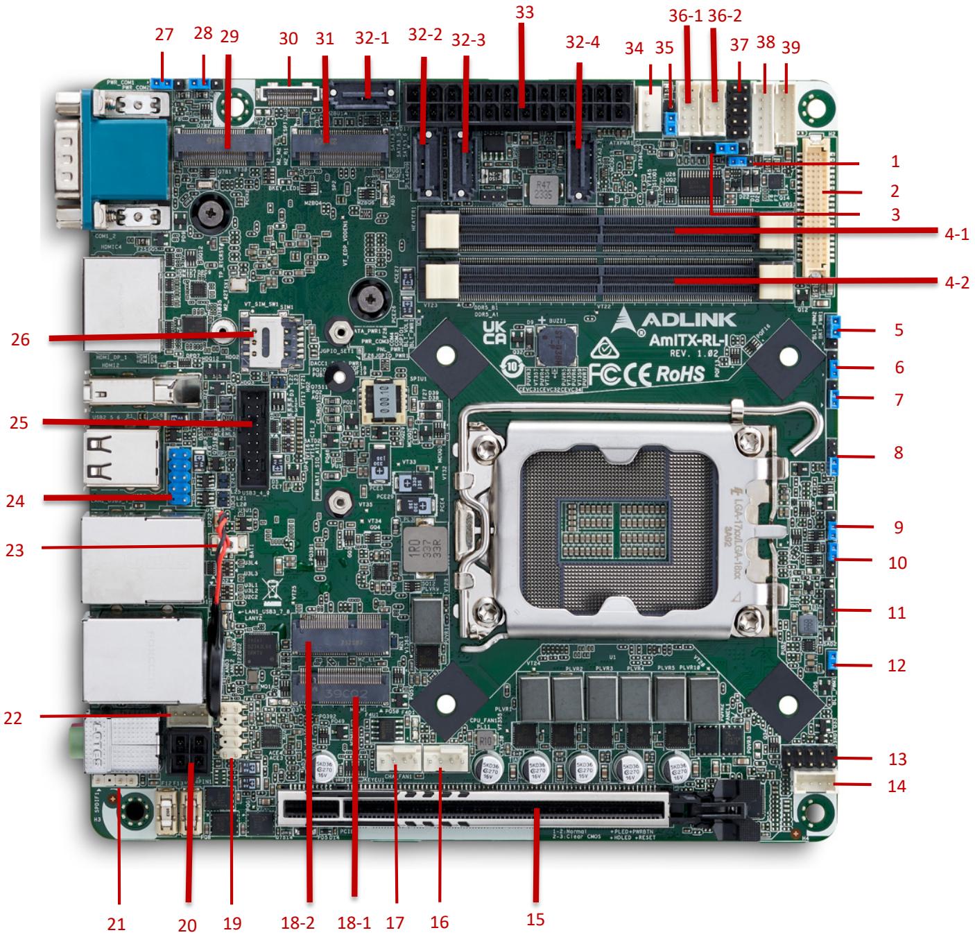
Figure 3: AmITX-RL-I component-side connectors .. ..10

# 1 Introduction

The AmITX-RL-I is a Mini-ITX motherboard supporting the Desktop 12th/13th/14th Generation Intel® Core™ i9/i7/i5/i3 and Pentium®/Celeron® Processor with Intel® Q670 Chipset. The AmITX-RL-I is specifically designed for customers who need high-level processing and graphics performance with a long product life solution.

The AmITX-RL-I features one DisplayPort, two HDMI, one LVDS or eDP, 2.5 and 1 Gigabit Ethernet ports, USB 3.2 Gen 2 and Gen 1 ports, USB 2.0 ports, and SATA 6 Gb/s ports. Expansion is provided by one PCIe Gen 5 x16 slot. The onboard feature connector provides GPIO, SMBus support. The board is equipped with SPI AMI EFI BIOS, supporting embedded features such as hardware monitor and watchdog timer

<table><tr><td>Model Number</td><td>Chipset</td></tr><tr><td>AmITX-RL-I</td><td>Q670</td></tr></table>

Latest revisions of the datasheet, user’s manual, BIOS, drivers, and board support packages, can be downloaded from the product webpage on the ADLINK web site: www.adlinktech.com

# 1.1 Packing List

• AmITX-RL-I Mini-ITX motherboard
Rear I/O shield
M.2 screws kit

# 1.2 Optional Accessories

CPU cooler for 65W CPU (P/N: 32-20976-0000-A0)
• USB 2.0 Cable (P/N: 30-21625-0000-B0)
• USB 3.0 Cable (P/N: 30-21597-1000-A0)
• SATA Cable (P/N: 30-10057-7000)
• SATA Power Cable (P/N: 30-22156-0000-A0)
COM Port Cable (P/N: 30-22155-0000-A0)

This page intentionally left blank.

# 2 Specifications

2.1 Core System

<table><tr><td rowspan="28">CPU</td><td colspan="6">Desktop 12th/13th/14th Generation Intel® CoreTM i9/i7/i5/i3 and Pentium®/Celeron® Processor, LGA1700 socket</td></tr><tr><td>Family</td><td>Number</td><td>CPU Core</td><td>Frequency (GHz)</td><td>Cache (MB)</td><td>Power</td></tr><tr><td>Alder Lake-S</td><td>i9-12900TE</td><td>16</td><td>1.1GHz</td><td>30MB</td><td>65W</td></tr><tr><td>Alder Lake-S</td><td>i9-12900E</td><td>16</td><td>2.3GHz</td><td>30MB</td><td>65W</td></tr><tr><td>Alder Lake-S</td><td>i7-12700TE</td><td>12</td><td>1.4GHz</td><td>25MB</td><td>35W</td></tr><tr><td>Alder Lake-S</td><td>i7-12700E</td><td>12</td><td>2.1GHz</td><td>25MB</td><td>65W</td></tr><tr><td>Alder Lake-S</td><td>i5-12500TE</td><td>6</td><td>1.9GHz</td><td>18MB</td><td>35W</td></tr><tr><td>Alder Lake-S</td><td>i5-12500E</td><td>6</td><td>2.9GHz</td><td>18MB</td><td>65W</td></tr><tr><td>Alder Lake-S</td><td>i3-12100TE</td><td>4</td><td>2.1GHz</td><td>12MB</td><td>35W</td></tr><tr><td>Alder Lake-S</td><td>i3-12100E</td><td>4</td><td>3.2GHz</td><td>12MB</td><td>60W</td></tr><tr><td>Alder Lake-S</td><td>G7400TE</td><td>2</td><td>3.0GHz</td><td>6MB</td><td>35W</td></tr><tr><td>Alder Lake-S</td><td>G7400E</td><td>2</td><td>3.6GHz</td><td>6MB</td><td>46W</td></tr><tr><td>Alder Lake-S</td><td>G6900TE</td><td>2</td><td>2.4GHz</td><td>4MB</td><td>35W</td></tr><tr><td>Alder Lake-S</td><td>G6900E</td><td>2</td><td>3.0GHz</td><td>4MB</td><td>46W</td></tr><tr><td>Raptor Lake-S</td><td>i9-13900TE</td><td>24</td><td>1.0GHz</td><td>36MB</td><td>35W</td></tr><tr><td>Raptor Lake-S</td><td>i9-13900E</td><td>24</td><td>1.8GHz</td><td>36MB</td><td>65W</td></tr><tr><td>Raptor Lake-S</td><td>i7-13700TE</td><td>16</td><td>1.1GHz</td><td>30MB</td><td>35W</td></tr><tr><td>Raptor Lake-S</td><td>i7-13700E</td><td>16</td><td>1.9GHz</td><td>30MB</td><td>65W</td></tr><tr><td>Raptor Lake-S</td><td>i5-13500TE</td><td>14</td><td>1.3GHz</td><td>24MB</td><td>35W</td></tr><tr><td>Raptor Lake-S</td><td>i5-13500E</td><td>14</td><td>2.4GHz</td><td>24MB</td><td>65W</td></tr><tr><td>Raptor Lake-S</td><td>i5-13400E</td><td>10</td><td>2.4GHz</td><td>20MB</td><td>65W</td></tr><tr><td>Raptor Lake-S</td><td>i3-13100TE</td><td>4</td><td>2.4GHz</td><td>12MB</td><td>35W</td></tr><tr><td>Raptor Lake-S</td><td>i3-13100E</td><td>4</td><td>3.3GHz</td><td>12MB</td><td>65W</td></tr><tr><td>Raptor Lake-S Refresh</td><td>i9-14900T</td><td>24</td><td>1.1GHz</td><td>36MB</td><td>35W</td></tr><tr><td>Raptor Lake-S Refresh</td><td>i9-14900</td><td>24</td><td>2.0GHz</td><td>36MB</td><td>65W</td></tr><tr><td>Raptor Lake-S Refresh</td><td>i7-14700T</td><td>20</td><td>1.3GHz</td><td>33MB</td><td>35W</td></tr><tr><td>Raptor Lake-S Refresh</td><td>i7-14700</td><td>20</td><td>2.1GHz</td><td>33MB</td><td>65W</td></tr><tr><td>Raptor Lake-S Refresh</td><td>i5-14500T</td><td>14</td><td>1.7GHz</td><td>24MB</td><td>35W</td></tr><tr><td rowspan="8"></td><td>Raptor Lake-S Refresh</td><td>i5-14500</td><td>14</td><td>2.6GHz</td><td>24MB</td><td>65W</td></tr><tr><td>Raptor Lake-S Refresh</td><td>i5-14400T</td><td>10</td><td>1.5GHz</td><td>20MB</td><td>35W</td></tr><tr><td>Raptor Lake-S Refresh</td><td>i5-14400</td><td>10</td><td>2.5GHz</td><td>20MB</td><td>65W</td></tr><tr><td>Raptor Lake-S Refresh</td><td>i3-14100T</td><td>4</td><td>2.7Ghz</td><td>12MB</td><td>35W</td></tr><tr><td>Raptor Lake-S Refresh</td><td>i3-14100</td><td>4</td><td>3.5GHz</td><td>12MB</td><td>60W</td></tr><tr><td>Raptor Lake-S Refresh</td><td>300T</td><td>2</td><td>3.4GHz</td><td>6MB</td><td>35W</td></tr><tr><td>Raptor Lake-S Refresh</td><td>300</td><td>2</td><td>3.9GHz</td><td>6MB</td><td>46W</td></tr><tr><td colspan="6">Note: Availability of features may vary between processor SKUs and operating systems.</td></tr><tr><td>Chipset</td><td colspan="6">Intel® Q670 Chipset</td></tr><tr><td>Memory</td><td colspan="6">Two 262-pin DDR5 non-ECC SODIMM slots, DDR5 4800 MHz, up to 64 GB (CPU dependent)</td></tr><tr><td>Embedded BIOS</td><td colspan="6">AMI® UEFI BIOS, 256Mb SPI flash memory</td></tr></table>

# 2.2 Rear I/O Connectors

<table><tr><td>Display</td><td>1x HDMI 2.0b, 1x HDMI 1.4b, 1x DP 1.4a</td></tr><tr><td>LAN</td><td>1x 1GbE RJ-451x 2.5GbE RJ-45</td></tr><tr><td>USB</td><td>4x USB3.2 Gen2 x12 x USB 2.0</td></tr><tr><td>Audio</td><td>1x Line-out, 1x Mic-in connector</td></tr><tr><td>Serial</td><td>2x RS-232/422/485</td></tr></table>

2.3 Internal Headers and Connectors

<table><tr><td>PCI Express Slots</td><td>1x PCIe Gen5 x16</td></tr><tr><td>USB</td><td>2x USB3.2 Gen1 x1 (via header)2x USB2.0 (via header)</td></tr><tr><td>SATA</td><td>4x SATA 6.0 Gb/s connectors. Software RAID support 0/1/5/10</td></tr><tr><td>Expansion Slots</td><td>1x M.2 B-key 3042/3052 (PCIe x1, USB3.2 Gen1, USB 2.0) for 4G/5G module1x M.2 E-key 2230 (PCIe x1, USB 2.0, CNVi) for Wireless1x M.2 M-Key 2242 (PCIe Gen3 x4) for SSD1x M.2 M-Key 2242/2280 (PCIe Gen4 x4) for SSD1x SIM socket connected to M.2 B Key</td></tr><tr><td>Serial</td><td>4x RS-232 headers</td></tr><tr><td>LVDS</td><td>1x LVDS pin header, supports single/dual channel 24-bit up to 1920x1200@60Hz (Connector shared with eDP)</td></tr><tr><td>DIO</td><td>1x 8-bit GPIO pin header</td></tr><tr><td>Other</td><td>ESPI HeaderCPU Fan ConnectorChassis Fan ConnectorSystem Panel HeaderFront Panel Audio HeaderChassis Intrusion HeaderSPDIF HeaderSpeaker HeaderSATA PWR OutputATX Power Connector, 12V DC-In co-design (4-pin)ATX Power Connector (24-pin)</td></tr></table>

# 2.4 Form Factor

Mini-ITX: 170mm x 170mm

# 2.5 Video

<table><tr><td>Controller</td><td>Intel® UHD Graphics</td></tr><tr><td>Display Interface Support</td><td>1x HDMI 2.0b, max resolution up to 4096x2160@60Hz1x HDMI 1.4b, max resolution up to 4096x2160@30Hz1x DP 1.4a, DP++, max resolution up to 4096x2160@60Hz1x LVDS, supports dual channel 24-bit, max resolution up to 1920x1200@60Hz (Connector shared with eDP)</td></tr></table>

# 2.6 Audio

<table><tr><td>Audio Codec</td><td>Realtek ALC897</td></tr><tr><td>Interfaces</td><td>1x Line-out, 1x Mic-in connector</td></tr></table>

# 2.7 LAN

<table><tr><td>Controller</td><td>1x Intel® i226-V with 10/100/1000/2500 Mbps1x Intel® i219-LM with 10/100/1000 Mbps, supports vPro</td></tr><tr><td>Interface</td><td>RJ45 connectors</td></tr></table>

# 2.8 Trusted Platform Module (TPM)

<table><tr><td>TPM 2.0</td><td>Infineon SLB9670XQ2.0</td></tr></table>

# 2.9 Power Specification

<table><tr><td>Input PWR</td><td>ATX PWR (24+4-pin) and +12V DC-In co-design</td></tr><tr><td>Power On</td><td>AT/ATX Supported- AT: Directly PWR on as power input ready- ATX: Press button to PWR on after power input ready</td></tr></table>

# 2.10 Watchdog Timer

<table><tr><td>Output</td><td>From Super I/O to drag RESETCON#</td></tr><tr><td>Interval</td><td>256 Segments, 0, 1, 2, ...255 Sec</td></tr></table>

# 2.11 Temperatures

<table><tr><td>Standard Operating Temperature</td><td>-20°C to 70°C</td></tr><tr><td>Storage Temperature</td><td>-40°C to 85°C</td></tr></table>

# 2.12 Environmental

<table><tr><td>Humidity</td><td>60°C @ 95% RH non-condensing</td></tr><tr><td>Vibration</td><td>1Grms, 5-500Hz, non-operation</td></tr></table>

# 2.13 Operating Systems

<table><tr><td>Standard Support</td><td>Microsoft® Windows® 10/11 64-bit, Ubuntu 22.04.4 LTS 64-bit</td></tr></table>

# 2.14 Functional Block Diagram

![Based on the provided block diagram, here is the accurate description of the labeled blocks and their connections:\n\n**Main Processing Blocks:**\n*   **Top Red Block:** Intel Alder Lake-S & Raptor Lake-S & Raptor Lake-S Refresh Processor LGA-1700\n*   **Middle Red Block:** Intel PCH Q670\n*   **Bottom Grey Block:** FINTEK F81966\n\n**Peripheral & Interface Blocks:**\n*   **Audio:** Realtek ALC897, Realtek ALC122\n*   **Bridge/Controller Chips:** ITE IT66318, Chrontel CH7513, Intel I219LM, Intel I226V, INFINEON SLB9670XQ2.0 TPM\n*   **Control/Management:** MCU\n*   **Connectors/Slots:** HDMI Connector (x2), Display port Connector, LVDS Connector, SO-DIMM (x2), PCIe x16 or x8/x8 Slot, SATA Port x4, M.2 Key M1, M.2 Key M2, M.2 Key E, M.2 Key B, SIM Card, BIOS, SMBus Header, Line Out Mic In, SPDIF, Front Audio, CPU FAN x1 CHA FAN x1, HW Monitor, LPT/DGIO header, COM Port x2 RS232/422/482, COM Port x2 RS232 only, SP339EER1 -L/TR x2, SP3243EUE Y-L/TR x2, 2x USB3.2 Gen2 Connector (x2), 2x USB3.2 Gen1 Header, RJ45 Connector (vPRO), RJ45 Connector, 2x USB2.0 Connector, 2x USB2.0 Header.\n\n**Connections:**\n\n**1. Intel Processor Connections:**\n*   Connects to **HDMI Connector** via **HDMI** -) **ITE IT66318** -) **DDI**\n*   Connects to **HDMI Connector** via **HDMI**\n*   Connects to **Display port Connector** via **DDI**\n*   Connects to **LVDS Connector** via **LVDS/eDP** -) **Chrontel CH7513** -) **DDI**\n*   Connects to **SO-DIMM** via **DDR5 4800/5600MHz** (two instances)\n*   Connects to **PCIe x16 or x8/x8 Slot** via **PCIe Gen5**\n*   Connects to **Intel PCH Q670** via **DMI**\n\n**2. Intel PCH Q670 Connections:**\n*   **Left Side (USB/Network):**\n    *   Connects to **2x USB3.2 Gen2 Connector** (two instances) via **2x USB3.2 Gen2**, **2x USB2.0**\n    *   Connects to **2x USB3.2 Gen1 Header** via **2x USB3.2 Gen1**, **2x USB2.0**\n    *   Connects to **RJ45 Connector (vPRO)** via **MDI 1G** -) **Intel I219LM** -) **PCIe x1**\n    *   Connects to **RJ45 Connector** via **MDI 2.5G** -) **Intel I226V** -) **PCIe x1**\n    *   Connects to **2x USB2.0 Connector** via **2x USB2.0**\n    *   Connects to **2x USB2.0 Header** via **2x USB2.0**\n    *   Connects to **MCU** via **SMBus**\n*   **Right Side (Storage/Expansion):**\n    *   Connects to **SATA Port x4** via **SATA**\n    *   Connects to **M.2 Key M1** via **PCIe x4 Gen4**\n    *   Connects to **M.2 Key M2** via **PCIe x4 Gen3**\n    *   Connects to **M.2 Key E** via **PCIe x1**, **CNVi**, **USB2.0**\n    *   Connects to **M.2 Key B** via **PCIe x1**, **USB3.2 Gen1**, **USB2.0**\n    *   Connects to **SIM Card** via **SIM** (attached to M.2 Key B)\n    *   Connects to **INFINEON SLB9670XQ2.0 TPM**\n    *   Connects to **BIOS** via **SPI**\n    *   Connects to **SMBus Header** via **SMBus**\n    *   Connects to **Realtek ALC897** via **HDA**\n*   **Bottom/Downward Connections:**\n    *   Connects to **LPT/DGIO header** via **GPIO x4** -) **LPT/GPIO** -) **FINTEK F81966**\n    *   Connects to **Realtek ALC122** (vertical link)\n    *   Connects to **FINTEK F81966** (vertical link)\n\n**3. FINTEK F81966 Connections:**\n*   Connects to **COM Port x2 RS232/422/482** via **SP339EER1 -L/TR x2** via **UART x2**\n*   Connects to **COM Port x2 RS232 only** via **SP3243EUE Y-L/TR x2** via **UART x4**\n*   Connects to **CPU FAN x1 CHA FAN x1** via **FAN**\n*   Connects to **HW Monitor**\n\n**4. Audio Connections:**\n*   **Realtek ALC897** connects to **Line Out Mic In**, **SPDIF**, and **Front Audio**.](.amitx-rl-i-50m-16008-1040-14/83c6192f4886d975e05ed7ecb57a5cb70e37971605b19b0742675a4489665da7.jpg)

Figure 1: AmITX-RL-I functional block diagram

# 3 Mechanical Layout

# 3.1 Connector Locations

# 3.1.1 Rear I/O Connectors

![A-1\nB\nC-1\nD-1\nD-2\nG-\nA-2\nE-1\nE-2\nC-2\nF-1 F-2\nF-3 F-4\nG-](.amitx-rl-i-50m-16008-1040-14/4ced2d874f54d2f19aa52de79cc566a549e80a4095af4f7f9b2741400a3bb469.jpg)

Figure 2: AmITX-RL-I rear I/O

<table><tr><td>Item</td><td>Description (Location)</td></tr><tr><td>A-1</td><td>COM Port (COM1) (RS232/422/485)</td></tr><tr><td>A-2</td><td>COM Port (COM2) (RS232/422/485)</td></tr><tr><td>B</td><td>DisplayPort (DP1)</td></tr><tr><td>C-1</td><td>USB 2.0 Port (USB3_5)</td></tr><tr><td>C-2</td><td>USB 2.0 Port (USB3_6)</td></tr><tr><td>D-1</td><td>RJ45 2.5GbE LAN Port (LAN2)</td></tr><tr><td>D-2</td><td>RJ45 GbE LAN Port (LAN1)</td></tr><tr><td>E-1</td><td>HDMI Port (HDMI1)</td></tr><tr><td>E-2</td><td>HDMI Port (HDMI2)</td></tr><tr><td>F-1</td><td>USB 3.2 Gen2 Port (USB3_2)</td></tr><tr><td>F-2</td><td>USB 3.2 Gen2 Port (USB3_1)</td></tr><tr><td>F-3</td><td>USB 3.2 Gen2 Port (USB3_8)</td></tr><tr><td>F-4</td><td>USB 3.2 Gen2 Port (USB3_7)</td></tr><tr><td>G-1</td><td>Audio Output: Green - Line Out</td></tr><tr><td>G-2</td><td>Audio Output: Pink - Mic In</td></tr></table>

# 3.1.2 Connectors and Jumpers

![27 28 29 30 31 32-1 32-2 32-3 33 32-4 34 35 36-1 36-2 37 38 39\nCOM1_2 HDM1C4 23.05V\nADLINK AmITX-RL-I REV. 1.02\nFCC CE RoHS\n1\n2\n3\n4-1\n4-2\n26\n5\n25\n6\n7\n8\n24\n9\n23\n10\n22\n11\n12\n13\n14\n21 20 19 18-2 18-1 17 16 15](.amitx-rl-i-50m-16008-1040-14/ca9af45731b064db2339348d637bb709550eb019ad36c05b445fc3f08d831a49.jpg)

Figure 3: AmITX-RL-I component-side connectors

<table><tr><td>Item</td><td>Description (Location)</td><td>Item</td><td>Description (Location)</td></tr><tr><td>1</td><td>Digital Input / Output Power Select (JGPIO_PWR1)</td><td>22</td><td>3W Audio AMP Output Wafer (SPEAKER1)</td></tr><tr><td>2</td><td>LVDS Panel Connector (LVDS1)</td><td>23</td><td>Battery Connector (BAT1)</td></tr><tr><td>3</td><td>Panel Power Select (LCD_VCC) (PNL_PWR1)</td><td>24</td><td>USB 2.0 Header (USB2_10_11)</td></tr><tr><td>4-1</td><td>DDR5_B1</td><td>25</td><td>USB 3.2 Gen1 Header (USB3_4_9)</td></tr><tr><td>4-2</td><td>DDR5_A1</td><td>26</td><td>SIM socket (SIM1)</td></tr><tr><td>5</td><td>Backlight Power Select (LCD_BLT_VCC) (BKT_PWR1)</td><td>27</td><td>COM Port PWR Setting Jumper (PWR_COM1 (For COM Port1))</td></tr><tr><td>6</td><td>CON_LBKLT_CTL Voltage Level (BLT_PWM2)</td><td>28</td><td>COM Port PWR Setting Jumper (PWR_COM2 (For COM Port2))</td></tr><tr><td>7</td><td>Digital Input / Output Default Value Setting (JGPIO_SET1)</td><td>29</td><td>M.2 M-Key 2242 slot (M2_M2)</td></tr><tr><td>8</td><td>DACC1_PCIE_PWR1</td><td>30</td><td>ESPI Header (ESPI1)</td></tr><tr><td>9</td><td>Clear CMOS Header (CLRMOS1)</td><td>31</td><td>M.2 B-Key 2242 slot (M2_B1)</td></tr><tr><td>10</td><td>Chassis Intrusion Header (CI1_2)</td><td>32-1</td><td>SATA3 Connectors (SATA3_4)</td></tr><tr><td>11</td><td>PWR_BAT1_SIO_AT1</td><td>32-2</td><td>SATA3 Connectors (SATA3_5)</td></tr><tr><td>12</td><td>Brightness Control Mode (BLT_PWM1)</td><td>32-3</td><td>SATA3 Connectors (SATA3_6)</td></tr><tr><td>13</td><td>System Panel Header (PANEL1)</td><td>32-4</td><td>SATA3 Connectors (SATA3_7)</td></tr><tr><td>14</td><td>SMBUS_TEST1</td><td>33</td><td>24-pin ATX Power Input Connector (ATXPWR1)</td></tr><tr><td>15</td><td>PCIe Gen5 x16 slot (PCIE1)</td><td>34</td><td>SATA Power Output Connector (SATA_PWR1)</td></tr><tr><td>16</td><td>CPU FAN Connector (+12V) (CPU_FAN1)</td><td>35</td><td>COM Port PWR Setting Jumper (PWR_COM3 (For COM Port3))</td></tr><tr><td>17</td><td>Chassis FAN Connector (+12V) (CHA_FAN1)</td><td>36-1</td><td>COM Port Headers (COM 4) (RS232)</td></tr><tr><td>18-1</td><td>M.2 M-Key 2242/2280 slot (M2_M1)</td><td>36-2</td><td>COM Port Headers (COM 3) (RS232)</td></tr><tr><td>18-2</td><td>M.2 E-Key 2230 slot (M2_E1)</td><td>37</td><td>Digital Input/Output Pin Header (JGPIO1)</td></tr><tr><td>19</td><td>Front Panel Audio Header (HD_AUDIO1)</td><td>38</td><td>Backlight Volume Control (BLT_VOL1)</td></tr><tr><td>20</td><td>4-pin ATX PWR Connector (DC_4PIN1)</td><td>39</td><td>Inverter Power Control Wafer (BLT_PWR1)</td></tr><tr><td>21</td><td>SPDIF Header (SPDIF1)</td><td colspan="2"></td></tr></table>

# 3.2 Thermal Solutions

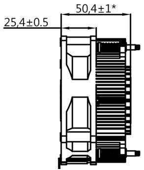
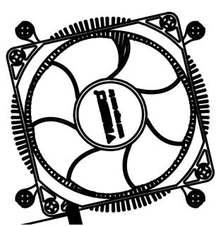
LGA1700 CPU Cooler, H=50.4mm, 65W

Standard Temp.: 0°C to 60°C

P/N: 32-20976-0000-A0
![Black-and-white illustration of a computer CPU fan with visible internal circuitry and mounting brackets (no text or symbols)](.amitx-rl-i-50m-16008-1040-14/befd3ba1afd6a12be33e04407c0923f84b325692d26cfe1cf3d54b9b1fd0d92a.jpg)

![25,4±0.5\n50,4±1*](.amitx-rl-i-50m-16008-1040-14/8dca72447c3012b3a40810363b495fee729ea5b82ca352e52779308854389e13.jpg)

This page intentionally left blank.

# 4 Connectors and Jumpers

See 3.1 Connector Locations on page 9.

# 4.1 Rear IO Connectors

# 4.1.1 DisplayPort

One DisplayPort 1.4a specification port up to 4096x2160@60Hz

<table><tr><td>Pin</td><td>Signal Name</td><td>Pin</td><td>Signal Name</td></tr><tr><td>1</td><td>DP1_CON_DP0</td><td>2</td><td>GND</td></tr><tr><td>3</td><td>DP1_CON_DN0</td><td>4</td><td>DP1_CON_DP1</td></tr><tr><td>5</td><td>GND</td><td>6</td><td>DP1_CON_DN1</td></tr><tr><td>7</td><td>DP1_CON_DP2</td><td>8</td><td>GND</td></tr><tr><td>9</td><td>DP1_CON_DN2</td><td>10</td><td>DP1_CON_DP3</td></tr><tr><td>11</td><td>GND</td><td>12</td><td>DP1_CON_DN3</td></tr><tr><td>13</td><td>DP1_HDMI_DNG_DET</td><td>14</td><td>DP_CFG2</td></tr><tr><td>15</td><td>DP1_CON_AUXP</td><td>16</td><td>GND</td></tr><tr><td>17</td><td>DP1_CON_AUXN</td><td>18</td><td>DP1_CON_HPD</td></tr><tr><td>19</td><td>GND</td><td>20</td><td>+3.3V</td></tr></table>

# 4.1.2 HDMI

One HDMI 2.0b specification port up to 4096 x 2160 @ 60 Hz

One HDMI 1.4b specification port up to 4096 x 2160 @ 30 Hz

<table><tr><td>Pin</td><td>Signal Name</td><td>Pin</td><td>Signal Name</td></tr><tr><td>1</td><td>HDMI1_CON_DP2</td><td>2</td><td>GND</td></tr><tr><td>3</td><td>HDMI1_CON_DN2</td><td>4</td><td>HDMI1_CON_DP1</td></tr><tr><td>5</td><td>GND</td><td>6</td><td>HDMI1_CON_DN1</td></tr><tr><td>7</td><td>HDMI1_CON_DP0</td><td>8</td><td>GND</td></tr><tr><td>9</td><td>HDMI1_CON_DN0</td><td>10</td><td>HDMI1_CON_CKP</td></tr><tr><td>11</td><td>GND</td><td>12</td><td>HDMI1_CON_CKN</td></tr><tr><td>13</td><td>N/C</td><td>14</td><td>N/C</td></tr><tr><td>15</td><td>HDMI1_DDC_CLK</td><td>16</td><td>HDMI1_DDC_DATA</td></tr><tr><td>17</td><td>GND</td><td>18</td><td>+5V</td></tr><tr><td>19</td><td>HDMI1_CON_HPD</td><td colspan="2"></td></tr></table>

![This is a technical line drawing of a rectangular electrical connector housing, likely a DB-20 connector. It features two vertical columns of small circular dots representing pins. The top-left pin is labeled with the number **1**, and the adjacent top-right pin is labeled **2**. Similarly, the bottom-left pin is labeled **19**, and the bottom-right pin is labeled **20**. The connector body has small rectangular notches on its left and right sides and a rounded cable entry point at the bottom.](.amitx-rl-i-50m-16008-1040-14/fb8f2c4f05048a29950c8690c386bc211a7599c0fee786267e33363558a646c2.jpg)

![19 17\n3 1\n18\n2](.amitx-rl-i-50m-16008-1040-14/655067788850464ddf29fd870f859ed1b608afdf4856a88bc2f3c75ff8fdb56d.jpg)

# 4.1.3 Ethernet Connectors (LAN1, LAN2)

LAN1: 10/100/1000/2500 Mbps LAN Ethernet controllers based on i226-LM.

LAN2: 10/100/1000 Mbps LAN Ethernet controllers based on i219-V, support vPro.

Both supporting PXE and WOL.

<table><tr><td>Pin</td><td>10BASE-T/100BASE-TX</td><td>1000BASE-T</td></tr><tr><td>1</td><td>TX+</td><td>LAN_MDI0+</td></tr><tr><td>2</td><td>TX-</td><td>LAN_MDI0-</td></tr><tr><td>3</td><td>RX+</td><td>LAN_MDI1+</td></tr><tr><td>4</td><td>--</td><td>LAN_MDI2+</td></tr><tr><td>5</td><td>--</td><td>LAN_MDI2-</td></tr><tr><td>6</td><td>RX-</td><td>LAN_MDI1-</td></tr><tr><td>7</td><td>--</td><td>LAN_MDI3+</td></tr><tr><td>8</td><td>--</td><td>LAN_MDI3-</td></tr></table>

ACT/LINK SPEED
![The image shows a close-up of a circuit board featuring two labels at the top reading 'LED' and 'LED' in black text. Vertical black lines connect the left label to a silver rectangular component and the right label to a copper-colored rectangular component. Below these smaller components sits a larger, black rectangular object. The background is a tan-colored printed circuit board.](.amitx-rl-i-50m-16008-1040-14/68e83c72fd8c3c6387e28b40e0f8d3c0c4a5bb6b3d0d6cd859c6fe62a9d498e7.jpg)

LED Behavior

<table><tr><td colspan="5">LAN2 LED Indications</td></tr><tr><td colspan="2">Activity Link LED</td><td></td><td colspan="2">SPEED LED</td></tr><tr><td>Status</td><td>Description</td><td rowspan="4"></td><td>Status</td><td>Description</td></tr><tr><td>Off</td><td>No Link</td><td>Off</td><td>10Mbps</td></tr><tr><td>On</td><td>Link</td><td>Orange</td><td>100Mbps</td></tr><tr><td>Blinking</td><td>Data Activity</td><td>Green</td><td>1Gbps connection</td></tr></table>

<table><tr><td colspan="5">LAN1 LED Indications</td></tr><tr><td colspan="2">Activity Link LED</td><td></td><td colspan="2">SPEED LED</td></tr><tr><td>Status</td><td>Description</td><td rowspan="4"></td><td>Status</td><td>Description</td></tr><tr><td>Off</td><td>No Link</td><td>Off</td><td>10Mbps</td></tr><tr><td>On</td><td>Link</td><td>Orange</td><td>100Mbps/1Gbps connection</td></tr><tr><td>Blinking</td><td>Data Activity</td><td>Green</td><td>2.5Gbps connection</td></tr></table>

# 4.1.4 USB Connectors

4x USB3.2 Gen2 x1, 2x USB2.0

<table><tr><td>Pin</td><td>Signal Name</td></tr><tr><td>1</td><td>+5VDC</td></tr><tr><td>2</td><td>USB_N</td></tr><tr><td>3</td><td>USB_P</td></tr><tr><td>4</td><td>GND</td></tr><tr><td>5</td><td>USB3_RX_N</td></tr><tr><td>6</td><td>USB3_RX_P</td></tr><tr><td>7</td><td>GND</td></tr><tr><td>8</td><td>USB3_TX_N</td></tr><tr><td>9</td><td>USB3_TX_P</td></tr></table>

![1\n2\n3\n4\n5\n6\n7\n8\n9](.amitx-rl-i-50m-16008-1040-14/a583da3c39a45a046ea1a318eccf6d705b13c0936f68a4d54738f15e43852022.jpg)

# 4.1.5 Serial COM Port Connector (COM1,2)

COM Port Pin Definition

COM1,2 supports RS-232/422/485, selected in BIOS.

<table><tr><td>Pin</td><td>RS232</td><td>RS422</td><td>RS485</td></tr><tr><td>1</td><td>DCD</td><td>TX-</td><td>RTX-</td></tr><tr><td>2</td><td>RXD</td><td>TX+</td><td>RTX+</td></tr><tr><td>3</td><td>TXD</td><td>RX+</td><td>N/A</td></tr><tr><td>4</td><td>DTR</td><td>RX-</td><td>N/A</td></tr><tr><td>5</td><td>GND</td><td>GND</td><td>GND</td></tr><tr><td>6</td><td>DSR</td><td>N/A</td><td>N/A</td></tr><tr><td>7</td><td>RTS</td><td>N/A</td><td>N/A</td></tr><tr><td>8</td><td>CTS</td><td>N/A</td><td>N/A</td></tr><tr><td>9</td><td>PWR</td><td>PWR</td><td>PWR</td></tr></table>

![1 2\n9](.amitx-rl-i-50m-16008-1040-14/d11a0840d8a5a70e1799485d6d728d5fb444a836505851f552171d89bd3bb38a.jpg)

# 4.1.6 Audio Connectors

• One Line-out, and one Mic-in on rear I/O
Realtek ALC897 codec

# 4.2 Internal Connectors

# 4.2.1 ATX Power Connector (ATXPWR1)

AmITX-RL-I supports a standard 24-pin ATX Power Connector (ATXPWR1)

<table><tr><td>Pin</td><td>Signal Name</td><td>Pin</td><td>Signal Name</td></tr><tr><td>1</td><td>+3V</td><td>13</td><td>+3V</td></tr><tr><td>2</td><td>+3V</td><td>14</td><td>-12V</td></tr><tr><td>3</td><td>GND</td><td>15</td><td>GND</td></tr><tr><td>4</td><td>+5V</td><td>16</td><td>PSON#</td></tr><tr><td>5</td><td>GND</td><td>17</td><td>GND</td></tr><tr><td>6</td><td>+5V</td><td>18</td><td>GND</td></tr><tr><td>7</td><td>GND</td><td>19</td><td>GND</td></tr><tr><td>8</td><td>PWROK_PS</td><td>20</td><td>NA</td></tr><tr><td>9</td><td>ATX+5VSB</td><td>21</td><td>+5V</td></tr><tr><td>10</td><td>+12V</td><td>22</td><td>+5V</td></tr><tr><td>11</td><td>+12V</td><td>23</td><td>+5V</td></tr><tr><td>12</td><td>+3V</td><td>24</td><td>GND</td></tr></table>

This motherboard provides a 24-pin ATX power connector. To use a 20-pin ATX power supply, please plug it along with Pin 1 and Pin 13.

# 4.2.2 ATX 12V Power Connector $( \mathsf { D C } \_ 4 \mathsf { P } \mathsf { I N } 1 )$

<table><tr><td>Pin</td><td>Signal Name</td></tr><tr><td>1</td><td>GND</td></tr><tr><td>2</td><td>GND</td></tr><tr><td>3</td><td>DC Input</td></tr><tr><td>4</td><td>DC Input</td></tr></table>

![The image displays a technical line drawing of a square connector interface, featuring a large outer square divided into a 2x2 grid of four smaller squares. Inside each smaller square is a central, solid black square. The top-left and bottom-right squares contain an additional outline shape resembling a contact terminal to the left of the central black square, while the top-right and bottom-left squares contain only the central black square.\n\nNumbers label the corners of the diagram:\n*   **1** is at the top right.\n*   **2** is at the bottom right.\n*   **3** is at the top left.\n*   **4** is at the bottom left.\n\nA vertical bracket connects the numbers **3** and **4** on the left side.](.amitx-rl-i-50m-16008-1040-14/bd3846809fd50054b0b9e888d2850bd4e94b8120267e8d420e28e7bd1ee56c2e.jpg)

# 4.2.3 SATA Connectors (SATA3\_4\~7)

Four SATA 6 Gbps ports are available on AmITX-RL-I.

The Serial ATA3 (SATA3) connector supports SATA data cables for internal storage devices. The current SATA3 interface allows up to 6.0 Gb/s data transfer rate.

<table><tr><td>Pin</td><td>Signal Name</td></tr><tr><td>1</td><td>GND</td></tr><tr><td>2</td><td>SATA-A+</td></tr><tr><td>3</td><td>SATA-A-</td></tr><tr><td>4</td><td>GND</td></tr><tr><td>5</td><td>SATA-B-</td></tr></table>

![1 7\nSATA3_4\n1\n7\nSATA3_5\n7\n1\nSATA3_6\nSATA3_7](.amitx-rl-i-50m-16008-1040-14/543b893fa9720a75e0303426bc4239a4bae6593a15ae9207ab70a0e05a50c0d5.jpg)

<table><tr><td>Pin</td><td>Signal Name</td></tr><tr><td>6</td><td>SATA-B+</td></tr><tr><td>7</td><td>GND</td></tr></table>

# 4.2.4 USB 2.0 Header (USB2\_10\_11)

2x USB 2.0.

The board provides one internal USB 2.0 header and the connector can support two USB 2.0. The maximum current per port is 0.5A.

<table><tr><td>Pin</td><td>Signal Name</td><td>Pin</td><td>Signal Name</td></tr><tr><td>1</td><td>USB_PWR</td><td>2</td><td>USB_PWR</td></tr><tr><td>3</td><td>P-</td><td>4</td><td>P-</td></tr><tr><td>5</td><td>P+</td><td>6</td><td>P+</td></tr><tr><td>7</td><td>GND</td><td>8</td><td>GND</td></tr><tr><td>9</td><td></td><td>10</td><td>DUMMY</td></tr></table>

![The image displays a schematic diagram of a 10-pin connector layout. A vertical rectangle encloses the pin positions. At the top left corner, there is a small black square notch. Inside the rectangle, there are ten positions arranged in five rows of two columns. The top-left position is a square shape containing a smaller square. The other visible positions are circles, but the bottom-left position is empty. The numbers '1' and '2' are positioned at the top left and top right, respectively. The numbers '9' and '10' are positioned at the bottom left and bottom right, respectively.](.amitx-rl-i-50m-16008-1040-14/fb078879d19f975b8a4c53cd20121b4252ae3cfeb2ce24faf772fa1fd9c46c2e.jpg)

# USB Cable (optional):

USB 2.0 Header to 2x Female Type-A Cable (length 150mm), P/N: 30-21625-0000-B0

![Pure electrical connector diagram showing internal cable and terminal block without any text or symbols](.amitx-rl-i-50m-16008-1040-14/18481b8d1da00103ac3e3f532267b09133a1ea1c98b84fe4eddc99b06231d1ad.jpg)

# 4.2.5 USB 3.2 Gen1 Header (USB3\_4\_9)

2x USB 3.2 Gen1

There is only a single USB 3.2 Gen1 connector on this motherboard. This header can support two USB 3.2

Gen1 ports with a maximum power current of 0.9A per port.

<table><tr><td>Pin</td><td>Signal Name</td><td>Pin</td><td>Signal Name</td></tr><tr><td>1</td><td>DUMMY</td><td>2</td><td>IntA_PA_D+</td></tr><tr><td>3</td><td>IntA_PB_D+</td><td>4</td><td>IntA_PA_D-</td></tr><tr><td>5</td><td>IntA_PB_D-</td><td>6</td><td>GND</td></tr><tr><td>7</td><td>GND</td><td>8</td><td>IntA_PA_SSTX+</td></tr><tr><td>9</td><td>IntA_PB_SSTX+</td><td>10</td><td>IntA_PA_SSTX-</td></tr><tr><td>11</td><td>IntA_PB_SSTX-</td><td>12</td><td>GND</td></tr><tr><td>13</td><td>GND</td><td>14</td><td>IntA_PA_SSRX+</td></tr><tr><td>15</td><td>IntA_PB_SSRX+</td><td>16</td><td>IntA_PA_SSRX-</td></tr><tr><td>17</td><td>IntA_PB_SSRX-</td><td>18</td><td>Vbus</td></tr><tr><td>19</td><td>Vbus</td><td>20</td><td></td></tr></table>

![1\n2\n19\n20](.amitx-rl-i-50m-16008-1040-14/3d414fc6d3e5e460bbc9362556a9c67161583c69918e6bf56f0b707dbc551194.jpg)

# USB Cable (optional):

USB 3.0 Header to 2x Female Type-A Cable (length 150mm), P/N: 30-21597-1000-A0

![Technical line drawing of a mechanical component with connector and terminal (no text or symbols)](.amitx-rl-i-50m-16008-1040-14/efe2a4b9dfcb63b30702ef36efea66471e53c8bebc15c4877ae7d7db61181510.jpg)

# 4.2.6 Front Panel Audio Header (HD\_AUDIO1)

This is a line out/microphone interface for the front panel audio cable that allows jack detection, and provides a convenient connection and control of audio devices.

<table><tr><td>Pin</td><td>Signal Name</td><td>Pin</td><td>Signal Name</td></tr><tr><td>1</td><td>MIC2_L</td><td>2</td><td>GND</td></tr><tr><td>3</td><td>MIC2_R</td><td>4</td><td></td></tr><tr><td>5</td><td>OUT2_R</td><td>6</td><td>MIC_RET</td></tr><tr><td>7</td><td>J_SENSE</td><td>8</td><td></td></tr><tr><td>9</td><td>OUT2_L</td><td>10</td><td>OUT_RET</td></tr></table>

![The image shows a schematic diagram of a 10-pin connector footprint. A vertical black rectangular outline encloses two columns of connection points. The left column consists of five circular holes arranged vertically. The right column consists of four circular holes and one square pad with a dot inside at the bottom position. Outside the rectangle, numbers indicate pin positions: '10' is at the top left corner, '9' is at the top right corner, '2' is at the bottom left corner, and '1' is at the bottom right corner.](.amitx-rl-i-50m-16008-1040-14/298a48d9c42cefa2d9a2dd3dcd1953bb53a49c781dc182c0c222383eeaf934e9.jpg)

# 4.2.7 CPU Fan and Chassis Fan Connectors (+12V) (CPU\_FAN1, CHA\_FAN1)

The board offers three 4-pin CPU fan (Smart Fan) connectors that are compatible with 3-pin CPU fan. If you connect a 3-pin CPU fan to the CPU fan connector on this motherboard, please connect it to pin 1-3. The maximum current is 1A.

<table><tr><td>Pin</td><td>Signal Name</td></tr><tr><td>1</td><td>GND</td></tr><tr><td>2</td><td>+12V</td></tr><tr><td>3</td><td>FAN_SPEED</td></tr><tr><td>4</td><td>FAN_SPEED_CONTROL</td></tr></table>

![The image displays a vertical rectangular outline on the left side, divided by a vertical line into a narrow left column and a wider right column. Inside the wider column, there is a square at the top, followed by three circles stacked vertically beneath it. To the right of the rectangle, the numbers 1, 2, 3, and 4 are arranged in a vertical column.](.amitx-rl-i-50m-16008-1040-14/cd5bbfc0eead93e6111865abb3ceca854d09717ad3e1819cd153fc8a34b1ad23.jpg)

# 4.2.8 Serial COM Port Connector (COM3,4)

Two internal serial ports (COM3,4). Serial ports are over-current protected.

<table><tr><td>Serial Port</td><td>Functions</td></tr><tr><td>COM3</td><td>Supports RS-232</td></tr><tr><td>COM4</td><td>Supports RS-232</td></tr></table>

# RS-232

There are two 2.54mm-pitch COM port headers (COM3\~COM4) that only support RS-232. The maximum current is 1A per port. The power supply of pin 9 is either 5V or 12V; Use the COM port pin 9 PWR Setting Jumper to control it.

(COM3)

<table><tr><td>Pin</td><td>Signal Name</td><td>Pin</td><td>Signal Name</td></tr><tr><td>1</td><td>DCD</td><td>2</td><td>RXD</td></tr><tr><td>3</td><td>TXD</td><td>4</td><td>DTR</td></tr><tr><td>5</td><td>GND</td><td>6</td><td>DSR</td></tr><tr><td>7</td><td>RTS</td><td>8</td><td>CTS</td></tr><tr><td>9</td><td>PWR</td><td>10</td><td></td></tr></table>

(COM4)

<table><tr><td>Pin</td><td>Signal Name</td><td>Pin</td><td>Signal Name</td></tr><tr><td>1</td><td>DCD</td><td>2</td><td>RXD</td></tr><tr><td>3</td><td>TXD</td><td>4</td><td>DTR</td></tr><tr><td>5</td><td>GND</td><td>6</td><td>DSR</td></tr><tr><td>7</td><td>RTS</td><td>8</td><td>CTS</td></tr><tr><td>9</td><td>N/A</td><td>10</td><td></td></tr></table>

![The image displays a pinout diagram for an electrical connector. Inside a central rectangular outline, there are two columns of pins arranged in five rows.\n\nOn the left side, the numbers **1**, **3**, **5**, **7**, and **9** are listed vertically. Small horizontal lines connect these numbers to the corresponding pins in the left column.\nOn the right side, the numbers **2**, **4**, **6**, and **8** are listed vertically. Small horizontal lines connect these numbers to the corresponding pins in the right column.\n\nThe pins inside the connector are described as follows:\n*   **Top Row:** A square shape (left, connected to 1) and a circle (right, connected to 2).\n*   **Second, Third, and Fourth Rows:** Two circles in each row.\n*   **Bottom Row:** A circle (left, connected to 9) and a circle with a horizontal line through it (right, below number 8, unnumbered).](.amitx-rl-i-50m-16008-1040-14/96f379ead67e747b80eee06d75e8955ee52b6c0b5f6f6e0183e9723503de520d.jpg)

# COM Cable (optional):

COM Port Cable (length 350mm), P/N: 30-22155-0000-A0

![Diagram of a long straight electrical connector with multiple internal wires, no text or symbols present](.amitx-rl-i-50m-16008-1040-14/d08ef0f746db85070289a928750a928e0dbc8e3dbd116c96b67330d56ca763ad.jpg)

# 4.2.9 LVDS Panel Connector (LVDS1)

<table><tr><td>Pin</td><td>Signal Name</td><td>Pin</td><td>Signal Name</td></tr><tr><td>1</td><td>LCD_VCC</td><td>2</td><td>LCD_VCC</td></tr><tr><td>3</td><td>+3.3V</td><td>4</td><td>NA</td></tr><tr><td>5</td><td>NA</td><td>6</td><td>LVDS_A_DATA0#</td></tr><tr><td>7</td><td>LVDS_A_DATA0</td><td>8</td><td>GND</td></tr><tr><td>9</td><td>LVDS_A_DATA1#</td><td>10</td><td>LVDS_A_DATA1</td></tr><tr><td>11</td><td>GND</td><td>12</td><td>LVDS_A_DATA2#</td></tr><tr><td>13</td><td>LVDS_A_DATA2</td><td>14</td><td>GND</td></tr><tr><td>15</td><td>LVDS_A_DATA3#</td><td>16</td><td>LVDS_A_DATA3</td></tr><tr><td>17</td><td>GND</td><td>18</td><td>LVDS_A_CLK#</td></tr><tr><td>19</td><td>LVDS_A_CLK</td><td>20</td><td>GND</td></tr><tr><td>21</td><td>LVDS_B_DATA0#</td><td>22</td><td>LVDS_B_DATA0</td></tr><tr><td>23</td><td>GND</td><td>24</td><td>LVDS_B_DATA1#</td></tr><tr><td>25</td><td>LVDS_B_DATA1</td><td>26</td><td>GND</td></tr><tr><td>27</td><td>LVDS_B_DATA2#</td><td>28</td><td>LVDS_B_DATA2</td></tr><tr><td>29</td><td>DPLVDD_EN</td><td>30</td><td>LVDS_B_DATA3#</td></tr><tr><td>31</td><td>LVDS_B_DATA3</td><td>32</td><td>GND</td></tr><tr><td>33</td><td>LVDS_B_CLK#</td><td>34</td><td>LVDS_B_CLK</td></tr><tr><td>35</td><td>GND</td><td>36</td><td>CON_LBKLT_EN</td></tr><tr><td>37</td><td>CON_LBKLT_CTL</td><td>38</td><td>LCD_BLT_VCC</td></tr><tr><td>39</td><td>LCD_BLT_VCC</td><td>40</td><td>LCD_BLT_VCC</td></tr></table>

![39\n40\n1\n2](.amitx-rl-i-50m-16008-1040-14/d6cd5916ae9ac4819e28b0983dace60ed01da506d7a9a7e706b2a60cb3fd6fa4.jpg)

\*eDP by pass mode pin definition (switch by BIOS)

<table><tr><td>Pin</td><td>Signal Name</td><td>Pin</td><td>Signal Name</td></tr><tr><td>1</td><td>LCD_VCC</td><td>2</td><td>LCD_VCC</td></tr><tr><td>3</td><td>N/A</td><td>4</td><td>N/A</td></tr><tr><td>5</td><td>N/A</td><td>6</td><td>N/A</td></tr><tr><td>7</td><td>N/A</td><td>8</td><td>GND</td></tr><tr><td>9</td><td>EDP_TX1#</td><td>10</td><td>EDP_TX1</td></tr><tr><td>11</td><td>GND</td><td>12</td><td>EDP_TX0#</td></tr><tr><td>13</td><td>EDP_TX0</td><td>14</td><td>GND</td></tr><tr><td>15</td><td>N/A</td><td>16</td><td>N/A</td></tr><tr><td>17</td><td>GND</td><td>18</td><td>EDP_AUXN</td></tr><tr><td>19</td><td>EDP_AUXP</td><td>20</td><td>GND</td></tr><tr><td>21</td><td>N/A</td><td>22</td><td>N/A</td></tr><tr><td>23</td><td>GND</td><td>24</td><td>N/A</td></tr><tr><td>25</td><td>N/A</td><td>26</td><td>GND</td></tr><tr><td>27</td><td>N/A</td><td>28</td><td>N/A</td></tr><tr><td>29</td><td>DPLVDD_EN</td><td>30</td><td>N/A</td></tr><tr><td>31</td><td>N/A</td><td>32</td><td>GND</td></tr><tr><td>33</td><td>N/A</td><td>34</td><td>N/A</td></tr><tr><td>35</td><td>GND</td><td>36</td><td>CON_LBKLT_EN</td></tr><tr><td>37</td><td>CON_LBKLT_CTL</td><td>38</td><td>LCD_BLT_VCC</td></tr><tr><td>39</td><td>LCD_BLT_VCC</td><td>40</td><td>LCD_BLT_VCC</td></tr></table>

# 4.2.10 System Panel Header (PANEL1)

This header accommodates several system front panel functions. Connect the power switch, reset switch, and system status indicator on the chassis to this header according to the pin assignments below. Note the positive and negative pins before connecting the cables.

<table><tr><td>Pin</td><td>Signal Name</td><td>Pin</td><td>Signal Name</td></tr><tr><td>1</td><td>HDLED+</td><td>2</td><td>PLED+</td></tr><tr><td>3</td><td>HDLED-</td><td>4</td><td>PLED-</td></tr><tr><td>5</td><td>GND</td><td>6</td><td>PWRBTN#</td></tr><tr><td>7</td><td>RESET#</td><td>8</td><td>GND</td></tr><tr><td>9</td><td>GND</td><td>10</td><td></td></tr></table>

![2\n10\n1\n9](.amitx-rl-i-50m-16008-1040-14/bdc19dc55f4cad8d62de25cc1cc98bbbaa2f6ab21c0683d9e1be30d763f7dcc6.jpg)

# PWRBTN (Power Switch):

Connect to the power switch on the chassis front panel. You may configure how to turn off your system using the power switch.

# RESET (Reset Switch):

Connect to the reset switch on the chassis front panel. Press the reset switch to restart the computer if the computer freezes and fails to perform a normal restart.

# PLED (System Power LED):

Connect to the power status indicator on the chassis front panel. The LED is turned on when the system is operating. The LED blinks when the system is in the S1 sleep state. The LED is off when the system is in the S3/S4 sleep state or powered off (S5).

# HDLED (Hard Drive Activity LED):

Connect to the hard drive activity LED on the chassis front panel. The LED is turned on when the hard drive is reading or writing data. The front panel design may differ by chassis. A front panel module mainly consists of power switch, reset switch, power LED, hard drive activity LED, speaker, etc. When connecting your chassis front panel module to this header, make sure the wire and the pin assignments are matched correctly.

# 4.2.11 Chassis Intrusion Header (CI1\_2)

This motherboard supports CASE OPEN detection feature that detects if the chassis cover has been removed. This feature requires a chassis with chassis intrusion detection design.

<table><tr><td>PIN 1-2 Open</td><td>Normal</td></tr><tr><td>PIN 1-2 Short</td><td>Active Case Open</td></tr><tr><td>PIN 3-4 Open</td><td>Active Case Open (Default)</td></tr><tr><td>PIN 3-4 Short</td><td>Normal</td></tr></table>

![The image shows a vertical rectangular outline containing four circular elements arranged in a column. The top three elements are simple concentric circles (rings). The bottom element is a concentric circle containing a square. To the right of the rectangle, the number '4' is aligned with the top element, and the number '1' is aligned with the bottom element.](.amitx-rl-i-50m-16008-1040-14/6545e1a174b8c919730065df2a764a6e8d8d98e5c6c453eae60ebef6b9b56af9.jpg)

# 4.2.12 ESPI Header (ESPI1)

The header is reserved for Port 80 code. display and debugging purposes.

<table><tr><td>Pin</td><td>Signal Name</td></tr><tr><td>1</td><td>GND</td></tr><tr><td>2</td><td>C_ESPI_CLK</td></tr><tr><td>3</td><td>GND</td></tr><tr><td>4</td><td>C_ESPI_CS#</td></tr><tr><td>5</td><td>DEBUG_RESET</td></tr><tr><td>6</td><td>GND</td></tr><tr><td>7</td><td>+3V</td></tr><tr><td>8</td><td>GND</td></tr><tr><td>9</td><td>SMB_CLK_MAIN</td></tr><tr><td>10</td><td>SMB_DATA_MAIN</td></tr><tr><td>11</td><td>C_ESPI_IO0</td></tr><tr><td>12</td><td>C_ESPI_IO1</td></tr><tr><td>13</td><td>C_ESPI_IO2</td></tr><tr><td>14</td><td>C_ESPI_IO3</td></tr><tr><td>15</td><td>GND</td></tr><tr><td>16</td><td>+3VSB</td></tr><tr><td>17</td><td>N/A</td></tr><tr><td>18</td><td>N/A</td></tr></table>

![The image features a thick black C-shaped outline at the top. Inside this outline is a row of approximately 30 thin, vertical, parallel black lines. Below the lines, the number '1' appears on the far left and the number '20' appears on the far right.](.amitx-rl-i-50m-16008-1040-14/e19878d3a8c9464f22c6b693c6ae2d4fb6b9968f6d13c45261f8743ce1a88e4c.jpg)

<table><tr><td>Pin</td><td>Signal Name</td></tr><tr><td>19</td><td>C_ESPI_ALERT#</td></tr><tr><td>20</td><td>GND</td></tr></table>

# 4.2.13 8-bit GPIO (JGPIO1)

<table><tr><td>Pin</td><td>Signal Name</td><td>Pin</td><td>Signal Name</td></tr><tr><td>1</td><td>SIO_GP71</td><td>2</td><td>GPP_H23</td></tr><tr><td>3</td><td>SIO_GP72</td><td>4</td><td>GPP_I10</td></tr><tr><td>5</td><td>SIO_GP73</td><td>6</td><td>GPP_E5</td></tr><tr><td>7</td><td>SIO_GP74</td><td>8</td><td>GPP_E6</td></tr><tr><td>9</td><td>JGPIOPWR_R</td><td>10</td><td>GND</td></tr></table>

![10\n9\n2\n1](.amitx-rl-i-50m-16008-1040-14/3810ca60843455f91add8c65a1e15cebf2d3f445c39eb5c5836e5013a71fd223.jpg)

# Output (Pin 1, 3, 5, 7)

<table><tr><td>Parameter</td><td>Range</td></tr><tr><td>GPIO output low voltage</td><td>Max: 0.4V</td></tr><tr><td>GPIO output high voltage</td><td>Low: 2.4V</td></tr><tr><td colspan="2">Note: Max. load per GPO pin: 12 mACurrent max. 1A per power pin</td></tr></table>

# Input (Pin 2, 4, 6, 8)

<table><tr><td>Parameter</td><td>Range</td></tr><tr><td>GPIO input low voltage</td><td>Max: 1V</td></tr><tr><td>GPIO input high voltage</td><td>Low: 2.3V</td></tr><tr><td colspan="2">Note: Max. load per GPI pin: 5μACurrent max. 1A per power pin</td></tr></table>

# 4.2.14 M.2 M-Key Socket (M2\_M2)

<table><tr><td>Pin</td><td>Signal Name</td><td>Pin</td><td>Signal Name</td></tr><tr><td>1</td><td>GND</td><td>2</td><td>+3.3V</td></tr><tr><td>3</td><td>GND</td><td>4</td><td>+3.3V</td></tr><tr><td>5</td><td>PERn3</td><td>6</td><td>NA</td></tr><tr><td>7</td><td>PERp3</td><td>8</td><td>NA</td></tr><tr><td>9</td><td>GND</td><td>10</td><td>LED</td></tr><tr><td>11</td><td>PETn3</td><td>12</td><td>+3.3V</td></tr><tr><td>13</td><td>PETp3</td><td>14</td><td>+3.3V</td></tr><tr><td>15</td><td>GND</td><td>16</td><td>+3.3V</td></tr><tr><td>17</td><td>PERn2</td><td>18</td><td>+3.3V</td></tr><tr><td>19</td><td>PERp2</td><td>20</td><td>NA</td></tr><tr><td>21</td><td>GND</td><td>22</td><td>NA</td></tr><tr><td>23</td><td>PETn2</td><td>24</td><td>NA</td></tr><tr><td>25</td><td>PETp2</td><td>26</td><td>NA</td></tr><tr><td>27</td><td>GND</td><td>28</td><td>NA</td></tr><tr><td>29</td><td>PERn1</td><td>30</td><td>NA</td></tr><tr><td>31</td><td>PERp1</td><td>32</td><td>NA</td></tr><tr><td>33</td><td>GND</td><td>34</td><td>NA</td></tr><tr><td>35</td><td>PETn1</td><td>36</td><td>NA</td></tr><tr><td>37</td><td>PETp1</td><td>38</td><td>DEVSLP</td></tr><tr><td>39</td><td>GND</td><td>40</td><td>SMB_CLK</td></tr><tr><td>41</td><td>PERn0</td><td>42</td><td>SMB_DATA</td></tr><tr><td>43</td><td>PERp0</td><td>44</td><td>NA</td></tr><tr><td>45</td><td>GND</td><td>46</td><td>NA</td></tr><tr><td>47</td><td>PETn0</td><td>48</td><td>NA</td></tr><tr><td>49</td><td>PETp0</td><td>50</td><td>PERST#</td></tr><tr><td>51</td><td>GND</td><td>52</td><td>CLKREQ#</td></tr><tr><td>53</td><td>PEFCLKn</td><td>54</td><td>NA</td></tr><tr><td>55</td><td>PEFCLKp</td><td>56</td><td>NA</td></tr><tr><td>57</td><td>GND</td><td>58</td><td>NA</td></tr><tr><td></td><td></td><td></td><td></td></tr><tr><td>67</td><td>NA</td><td>68</td><td>NA</td></tr><tr><td>69</td><td>PEDET</td><td>70</td><td>+3.3V</td></tr><tr><td>71</td><td>GND</td><td>72</td><td>+3.3V</td></tr><tr><td>73</td><td>GND</td><td>74</td><td>+3.3V</td></tr><tr><td>75</td><td>GND</td><td></td><td></td></tr></table>

4.2.15 M.2 M-Key Socket (M2\_M2)

<table><tr><td>Pin</td><td>Signal Name</td><td>Pin</td><td>Signal Name</td></tr><tr><td>1</td><td>NA</td><td>2</td><td>+3.3V</td></tr><tr><td>3</td><td>GND</td><td>4</td><td>+3.3V</td></tr><tr><td>5</td><td>GND</td><td>6</td><td>FuLL Card_Power_</td></tr><tr><td></td><td></td><td></td><td>off</td></tr><tr><td>7</td><td>USB_D+</td><td>8</td><td>W_DISABLE</td></tr><tr><td>9</td><td>USB_D-</td><td>10</td><td>WWAN_LED#</td></tr><tr><td>11</td><td>GND</td><td></td><td></td></tr><tr><td></td><td></td><td></td><td></td></tr><tr><td>21</td><td>GND</td><td>20</td><td>NA</td></tr><tr><td>23</td><td>NA</td><td>22</td><td>NA</td></tr><tr><td>25</td><td>NA</td><td>24</td><td>NA</td></tr><tr><td>27</td><td>GND</td><td>26</td><td>NA</td></tr><tr><td>29</td><td>USB3_RX-</td><td>28</td><td>NA</td></tr><tr><td>31</td><td>USB3_RX+</td><td>30</td><td>UIM_RESET</td></tr><tr><td>33</td><td>GND</td><td>32</td><td>UIM_CLK</td></tr><tr><td>35</td><td>USB3_TX-</td><td>34</td><td>UIM_DATA</td></tr><tr><td>37</td><td>USB3_TX+</td><td>36</td><td>UIM_PWR</td></tr><tr><td>39</td><td>GND</td><td>38</td><td>NA</td></tr><tr><td>41</td><td>PERn0</td><td>40</td><td>NA</td></tr><tr><td>43</td><td>PERP0</td><td>42</td><td>NA</td></tr><tr><td>45</td><td>GND</td><td>44</td><td>NA</td></tr><tr><td>47</td><td>PETn0</td><td>46</td><td>NA</td></tr><tr><td>49</td><td>PETP0</td><td>48</td><td>NA</td></tr><tr><td>51</td><td>GND</td><td>50</td><td>PERST#</td></tr><tr><td>53</td><td>PEFCLKn</td><td>52</td><td>CLKREQ#</td></tr><tr><td>55</td><td>PEFCLKp</td><td>54</td><td>NA</td></tr><tr><td>57</td><td>GND</td><td>56</td><td>NA</td></tr><tr><td>59</td><td>NA</td><td>58</td><td>NA</td></tr><tr><td>61</td><td>NA</td><td>60</td><td>NA</td></tr><tr><td>63</td><td>NA</td><td>62</td><td>NA</td></tr><tr><td>65</td><td>NA</td><td>64</td><td>NA</td></tr><tr><td>67</td><td>NA</td><td>66</td><td>NA</td></tr><tr><td>69</td><td>NA</td><td>68</td><td>NA</td></tr><tr><td>71</td><td>GND</td><td>70</td><td>+3.3V</td></tr><tr><td>73</td><td>GND</td><td>72</td><td>+3.3V</td></tr><tr><td>75</td><td>NA</td><td>74</td><td>+3.3V</td></tr></table>

4.2.16 M.2 Mkey Socket (M2\_M1)

<table><tr><td>Pin</td><td>Signal Name</td><td>Pin</td><td>Signal Name</td></tr><tr><td>1</td><td>GND</td><td>2</td><td>+3.3V</td></tr><tr><td>3</td><td>GND</td><td>4</td><td>+3.3V</td></tr><tr><td>5</td><td>PERn3</td><td>6</td><td>NA</td></tr><tr><td>7</td><td>PERp3</td><td>8</td><td>NA</td></tr><tr><td>9</td><td>GND</td><td>10</td><td>SATA_LED</td></tr><tr><td>11</td><td>PETn3</td><td>12</td><td>+3.3V</td></tr><tr><td>13</td><td>PETp3</td><td>14</td><td>+3.3V</td></tr><tr><td>15</td><td>GND</td><td>16</td><td>+3.3V</td></tr><tr><td>17</td><td>PERn2</td><td>18</td><td>+3.3V</td></tr><tr><td>19</td><td>PERp2</td><td>20</td><td>NA</td></tr><tr><td>21</td><td>GND</td><td>22</td><td>NA</td></tr><tr><td>23</td><td>PETn2</td><td>24</td><td>NA</td></tr><tr><td>25</td><td>PETp2</td><td>26</td><td>NA</td></tr><tr><td>27</td><td>GND</td><td>28</td><td>NA</td></tr><tr><td>29</td><td>PERn1</td><td>30</td><td>NA</td></tr><tr><td>31</td><td>PERp1</td><td>32</td><td>NA</td></tr><tr><td>33</td><td>GND</td><td>34</td><td>NA</td></tr><tr><td>35</td><td>PETn1</td><td>36</td><td>NA</td></tr><tr><td>37</td><td>PETp1</td><td>38</td><td>NA</td></tr><tr><td>39</td><td>GND</td><td>40</td><td>SMB_CLK</td></tr><tr><td>41</td><td>PERn0</td><td>42</td><td>SMB_DATA</td></tr><tr><td>43</td><td>PERp0</td><td>44</td><td>NA</td></tr><tr><td>45</td><td>GND</td><td>46</td><td>NA</td></tr><tr><td>47</td><td>PETn0</td><td>48</td><td>NA</td></tr><tr><td>49</td><td>PETp0</td><td>50</td><td>PERST#</td></tr><tr><td>51</td><td>GND</td><td>52</td><td>CLKREQ#</td></tr><tr><td>53</td><td>PEFCLKn</td><td>54</td><td>NA</td></tr><tr><td>55</td><td>PEFCLKp</td><td>56</td><td>NA</td></tr><tr><td>57</td><td>GND</td><td>58</td><td>NA</td></tr><tr><td></td><td></td><td></td><td></td></tr><tr><td>67</td><td>NA</td><td>68</td><td>NA</td></tr><tr><td>69</td><td>PEDET</td><td>70</td><td>+3.3V</td></tr><tr><td>71</td><td>GND</td><td>72</td><td>+3.3V</td></tr><tr><td>73</td><td>GND</td><td>0</td><td>+3.3V</td></tr><tr><td>75</td><td>GND</td><td></td><td></td></tr></table>

4.2.17 M.2 E-Key Socket (M2\_E1)

<table><tr><td>Pin</td><td>Signal Name</td><td>Pin</td><td>Signal Name</td></tr><tr><td>1</td><td>GND</td><td>2</td><td>+3.3V</td></tr><tr><td>3</td><td>USB_D+</td><td>4</td><td>+3.3V</td></tr><tr><td>5</td><td>USB_D-</td><td>6</td><td>NA</td></tr><tr><td>7</td><td>GND</td><td>8</td><td>NA</td></tr><tr><td>9</td><td>CNV_WGR_D1-</td><td>10</td><td>CNV_RF_RESET</td></tr><tr><td>11</td><td>CNV_WGR_D1+</td><td>12</td><td>NA</td></tr><tr><td>13</td><td>GND</td><td>14</td><td>MODEM_CLKREQ</td></tr><tr><td>15</td><td>CNV_WGR_D0-</td><td>16</td><td>NA</td></tr><tr><td>17</td><td>CNV_WGR_D0+</td><td>18</td><td>GND</td></tr><tr><td>19</td><td>GND</td><td>20</td><td>NA</td></tr><tr><td>21</td><td>CNV_WGR_CLK-</td><td>22</td><td>CNV_BRI_RSP</td></tr><tr><td>23</td><td>CNV_WGR_CLK+</td><td></td><td></td></tr><tr><td></td><td></td><td></td><td></td></tr><tr><td>33</td><td>GND</td><td>32</td><td>CNV_BGI_DT</td></tr><tr><td>35</td><td>PETp</td><td>34</td><td>CNV_RGI_RSP</td></tr><tr><td>37</td><td>PETn</td><td>36</td><td>CNV_BRI_DT</td></tr><tr><td>39</td><td>GND</td><td>38</td><td>NA</td></tr><tr><td>41</td><td>PERp</td><td>40</td><td>NA</td></tr><tr><td>43</td><td>PERn</td><td>42</td><td>NA</td></tr><tr><td>45</td><td>GND</td><td>44</td><td>NA</td></tr><tr><td>47</td><td>PEFCLKp</td><td>46</td><td>NA</td></tr><tr><td>49</td><td>PEFCLKn</td><td>48</td><td>NA</td></tr><tr><td>51</td><td>GND</td><td>50</td><td>SUSCLK</td></tr><tr><td>53</td><td>CLKREQ#</td><td>52</td><td>PERST0#</td></tr><tr><td>55</td><td>NA</td><td>54</td><td>W_DISABLE1#</td></tr><tr><td>57</td><td>GND</td><td>56</td><td>W_DISABLE2#</td></tr><tr><td>59</td><td>CNV_WT_D1-</td><td>58</td><td>SMB_DATA</td></tr><tr><td>61</td><td>CNV_WT_D1+</td><td>60</td><td>SMB_CLK</td></tr><tr><td>63</td><td>GND</td><td>62</td><td>NA</td></tr><tr><td>65</td><td>CNV_WT_D0-</td><td>64</td><td>NA</td></tr><tr><td>67</td><td>CNV_WT_D0+</td><td>66</td><td>NA</td></tr><tr><td>69</td><td>GND</td><td>68</td><td>NA</td></tr><tr><td>71</td><td>CNV_WT_CLK-</td><td>70</td><td>NA</td></tr><tr><td>73</td><td>CNV_WT_CLK+</td><td>72</td><td>+3.3V</td></tr><tr><td>75</td><td>GND</td><td>74</td><td>+3.3V</td></tr></table>

# 4.3 Jumper and Switch Settings

# 4.3.1 PWR\_BAT1\_SIO\_AT1

Only supported by chargeable battery.

<table><tr><td>PIN 1-2 Open</td><td>Normal</td></tr><tr><td>PIN 1-2 Short</td><td>Charge Battery</td></tr><tr><td>PIN 3-4 Open</td><td>ATX Mode</td></tr><tr><td>PIN 3-4 Short</td><td>AT Mode</td></tr></table>

![The image displays a vertical black rectangular border containing a column of shapes. The top three shapes are circles, and the bottom shape is a square. To the right of the border, the number '4' is aligned horizontally with the top circle, and the number '1' is aligned horizontally with the bottom square.](.amitx-rl-i-50m-16008-1040-14/b5cd474215b4ee3637774a41095eabd08b91ce5e161584bcb6a1bad8a5dd6ea5.jpg)

# 4.3.2 Clear CMOS Header (CLRMOS1)

<table><tr><td>1-2</td><td>Normal (Default)</td></tr><tr><td>2-3</td><td>Clear CMOS</td></tr></table>

![This image displays a schematic diagram of a connector with three pins. On the left, a vertical rectangular outline contains three connection symbols arranged vertically: two open circles at the top and a square containing a smaller square dot at the bottom. To the right of the outline, the numbers 3, 2, and 1 are listed vertically, corresponding respectively to the top circle, the middle circle, and the bottom square symbol.](.amitx-rl-i-50m-16008-1040-14/d9c0884041890162fd766637b834371ed097727fa2ca99a792a310c4d45cde8e.jpg)

# 4.3.3 Brightness Control Mode (BLT\_PWM1)

Please set to 1-2 when adjusting brightness by Brightness Control bar under OS.

Please set to 2-3 when adjusting brightness by BLT\_VOL1.

<table><tr><td>1-2</td><td>From eDP PWM to CON_LBKLT_CTL</td></tr><tr><td>2-3</td><td>From LVDS PWM to CON_LBKLT_CTL (Default)</td></tr></table>

![The image displays a vertical rectangular outline on the left containing three shapes stacked vertically. At the top is a circle, followed by another circle in the middle, and a square-within-a-square shape at the bottom. To the right of the rectangle, the numbers 3, 2, and 1 are listed vertically, aligning with the top, middle, and bottom shapes respectively.](.amitx-rl-i-50m-16008-1040-14/621bbc5e25d85959658d603820b6d3b17b7f2245c979131a57999f720c5d765b.jpg)

# 4.3.4 COM Port PWR Setting Jumpers

PWR\_COM1 (For COM Port1)

PWR\_COM2 (For COM Port2)

PWR\_COM3 (For COM Port3)

The maximum current per port is 1A and the power supply is either 5V or 12V. Use the jumpers to set the power for COM port pin 9.

<table><tr><td>1-2</td><td>Normal (Default)</td></tr><tr><td>2-3</td><td>Clear CMOS</td></tr></table>

![The image displays a black-and-white schematic diagram. A rectangular outline encloses three distinct shapes arranged horizontally. On the far left is a square containing a smaller shape (appearing to be a square or circle). To its right are two hollow circles. Below the rectangular outline, the numbers '1', '2', and '3' are printed, each aligned beneath the corresponding shape.](.amitx-rl-i-50m-16008-1040-14/debe52ed4705e40da8629cb89752d98d0b5d1d81d07a5bc52dff42e454b04e10.jpg)

# 4.3.5 SATA Power Output Connector (SATA\_PWR1)

<table><tr><td>Pin</td><td>Signal Name</td></tr><tr><td>1</td><td>+5V</td></tr><tr><td>2</td><td>GND</td></tr><tr><td>3</td><td>GND</td></tr><tr><td>4</td><td>+12V</td></tr></table>

![The image displays a vertical white rectangle containing four circles stacked vertically. The top three circles are empty, while the bottom circle contains a square. To the right of the rectangle, the number '4' is aligned near the top circle, and the number '1' is aligned near the bottom circle. A thick black vertical bar runs along the far left edge.](.amitx-rl-i-50m-16008-1040-14/cfe1d044f1ff16b5587d43fd2c25cae27af5edcee1c823371a69408be15b18d2.jpg)

# 4.3.6 Backlight Volume Control (BLT\_VOL1)

<table><tr><td>Pin</td><td>Signal Name</td></tr><tr><td>1</td><td>GPIO_VOL_UP</td></tr><tr><td>2</td><td>GPIO_VOL_DW</td></tr><tr><td>3</td><td>PWRDN</td></tr><tr><td>4</td><td>BLT_UP</td></tr><tr><td>5</td><td>BLT_DW</td></tr><tr><td>6</td><td>GND</td></tr><tr><td>7</td><td>GND</td></tr></table>

![The image displays a technical schematic of a connector. On the left, a vertical rectangular outline contains a column of six circular holes; the bottom-most hole is enclosed within a square. To the right, separated by a vertical line, are the numbers 7 and 1, aligned with the top and bottom rows respectively.](.amitx-rl-i-50m-16008-1040-14/5e7f23207e79cadc125f8cb9201711311208d9b5f992eb90d25e7a93a7e8c153.jpg)

# 4.3.7 Inverter Power Control Wafer (BLT\_PWR1)

<table><tr><td>Pin</td><td>Signal Name</td></tr><tr><td>1</td><td>GND</td></tr><tr><td>2</td><td>GND</td></tr><tr><td>3</td><td>CON_LBKLT_CTL</td></tr><tr><td>4</td><td>CON_LBKLT_EN</td></tr><tr><td>5</td><td>LCD_BLT_VCC</td></tr><tr><td>6</td><td>LCD_BLT_VCC</td></tr></table>

![The image displays a schematic diagram of a connector, shown as a vertical rectangular outline. Inside, there is a column of six pin positions: five are circular holes, and the bottom-most position is a square. On the right side, the number '6' is aligned with the top pin, and the number '1' is aligned with the bottom pin.](.amitx-rl-i-50m-16008-1040-14/e8f221fdfa41e35f8d95483cd960db1c83653bda7bb8ccb385335d1cb0fd08e0.jpg)

# 4.3.8 Digital Input / Output Power Select (JGPIO\_PWR1)

The maximum current JGPIO\_PWR1 provides is 1A.

<table><tr><td>1-2</td><td>+12V</td></tr><tr><td>2-3</td><td>+5V (Default)</td></tr></table>

![A horizontal rectangular outline with rounded corners encloses a square icon on the far left and two simple circles to its right. Below the rectangle, the numbers 1, 2, and 3 are aligned beneath each corresponding shape.](.amitx-rl-i-50m-16008-1040-14/ab1cf4a3b8fc6f2c770492d4093936835c46c5a391e2a65147898634dd49da45.jpg)

# 4.3.9 Panel Power Select (LCD\_VCC)

(PNL\_PWR1)

Use this to set up the VDD power of the LVDS connector.

<table><tr><td>1-2</td><td>LCD_VCC: +3V (Default)</td></tr><tr><td>2-3</td><td>LCD_VCC: +5V</td></tr><tr><td>4-5</td><td>LCD_VCC: +12V</td></tr></table>

![The image features a horizontal rectangular outline containing five circular elements. The first four elements are hollow circles. The fifth element, on the far right, is a black circle enclosed within a small square. Below the left end of the rectangle is the number '5', and below the right end is the number '1'.](.amitx-rl-i-50m-16008-1040-14/9da90848a71fd92b92295690ce4d1366634b7ac6d34fff61daa3811ccb273e49.jpg)

# 4.3.10 Backlight Power Select (LCD\_BLT\_VCC)

(BKT\_PWR1)

Use this header to set up the backlight power of the LVDS connector and the panel backlight power of BLT\_PWM1.

<table><tr><td>1-2</td><td>LCD_BLT_VCC: +5V(Default)</td></tr><tr><td>2-3</td><td>LCD_BLT_VCC: +12V</td></tr></table>

![The image displays a vertical list of three items. On the left, inside a tall rectangular border, there are three shapes stacked vertically: a circle at the top, a circle in the middle, and a square containing a circle at the bottom. To the right of these shapes, aligned vertically, are the numbers 3, 2, and 1.](.amitx-rl-i-50m-16008-1040-14/43d2b5fc8895ca066757502c44fbe8e048a67cb88ed711b5aaad778603c4bae2.jpg)

# 4.3.11 CON\_LBKLT\_CTL Voltage Level (BLT\_PWM2)

<table><tr><td>1-2</td><td>3V Level (Default)</td></tr><tr><td>2-3</td><td>5V Level</td></tr></table>

![The image features a vertical rectangular outline containing three elements arranged in a column. The top two elements are simple circles, while the bottom element is a square containing a circle. To the right of the rectangle, the numbers 3, 2, and 1 are listed vertically, aligned with the top, middle, and bottom elements respectively.](.amitx-rl-i-50m-16008-1040-14/7313963fdffd108e51d57077a47a18916ddc719083136d9a8a58180dfc50f827.jpg)

# 4.3.12 Digital Input / Output Default Value Setting (JGPIO\_SET1)

The header is used for GPIO default value setting for either pull high or pull low. Pulling the header to a high/low value means the voltage is anchored to VCC/GND, in a stable, non-floating state.

<table><tr><td>1-2</td><td>Pull-High (Default)</td></tr><tr><td>2-3</td><td>Pull-Low</td></tr></table>

![The image displays a vertical rectangular frame containing three circles arranged vertically. To the right of the frame, the numbers 3, 2, and 1 appear next to the top, middle, and bottom circles respectively. The bottom circle contains a square inside it.](.amitx-rl-i-50m-16008-1040-14/3c925c49a65f44bee993606eb9a2ef1af3d9c17a4ff2db5db3d706848d245d84.jpg)

# 4.3.13 DACC1\_PCIE\_PWR1

Auto clear CMOS when system boot improperly.

<table><tr><td>PIN1-2 Open</td><td>No ACC (Default)</td></tr><tr><td>PIN1-2 Short</td><td>ACC</td></tr><tr><td>PIN3</td><td>PSON#</td></tr><tr><td>PIN4</td><td>GND</td></tr></table>

![The image displays a schematic diagram of a vertical connector. Inside a rectangular outline, there are four circular symbols arranged in a column. The top three symbols are simple circles. The bottom symbol is a square containing a circle, with a small white square in its upper right corner. To the right of the connector, the number '4' is aligned with the top position and the number '1' is aligned with the bottom position.](.amitx-rl-i-50m-16008-1040-14/d724edc6cc1a7df6b479c8ee6344acf17f8010112bf5dd19e82030434e0fda3b.jpg)

# 4.3.14 SMBUS\_TEST1

<table><tr><td>Pin</td><td>Signal Name</td></tr><tr><td>1</td><td>GPP_E7</td></tr><tr><td>2</td><td>SMB_CLK_MAIIIN</td></tr><tr><td>3</td><td>SMB_DATA_MAIN</td></tr><tr><td>4</td><td>GND</td></tr></table>

![The image displays a schematic diagram of a connector. At the top, a rectangular outline contains four circular holes arranged in a horizontal row. The hole on the far right is a square. Below the connector outline, the number '4' is visible on the left side, and the number '1' is visible on the right side.](.amitx-rl-i-50m-16008-1040-14/5b36643a9ddbc7a6cdc5954b248069a0dad33ba883c51fc27a42218cd8dc7109.jpg)

# 4.3.15 SPDIF Header (SPDIF1)

SPDIF header, providing SPDIF audio output to HDMI VGA card, allows the system to connect HDMI Digital TV/projector/LCD devices. Please connect the SPDIF connector of HDMI VGA card to this header.

<table><tr><td>Pin</td><td>Signal Name</td></tr><tr><td>1</td><td>+5V</td></tr><tr><td>2</td><td></td></tr><tr><td>3</td><td>SPDIF OUT</td></tr><tr><td>4</td><td>GND</td></tr></table>

![The image displays a horizontal rectangular control bar or timeline interface. Inside the bar, on the far left, is a square containing a circle. To the right, there are two open circles side-by-side. Below the bar, the number '1' is positioned under the left square, and the number '4' is positioned under the circles on the right.](.amitx-rl-i-50m-16008-1040-14/30aee7fb9d714175989bd60134aa135ebbcf3255c19096f35d7ec4b9f8f02e20.jpg)

# 4.3.16 3W Audio AMP Output Wafer (SPEAKER1)

<table><tr><td>Pin</td><td>Signal Name</td></tr><tr><td>1</td><td>OUTLN</td></tr><tr><td>2</td><td>OUTLP</td></tr><tr><td>3</td><td>OUTRP</td></tr><tr><td>4</td><td>OUTRN</td></tr></table>

![A black and white line drawing depicts a horizontal rectangle containing four circles arranged in a row. The leftmost circle contains a smaller square, while the other three circles are empty. Below the rectangle, the number '1' appears on the left and the number '4' appears on the right.](.amitx-rl-i-50m-16008-1040-14/114b11b9b68070128ebc5ef4f6ff73b11ff68cfd36f94cb36869b00c87944d68.jpg)

# 4.3.17 Battery Connector (BAT1)

<table><tr><td>Pin</td><td>Signal Name</td></tr><tr><td>1</td><td>+BAT</td></tr><tr><td>2</td><td>GND</td></tr></table>

![The image displays a black-and-white line drawing of a connector or socket. In the center is a rectangular box containing two circles side-by-side. Flanking the central box are two vertical rectangular sections, one on the left and one on the right. Below the left section is the number '1' and below the right section is the number '2'.](.amitx-rl-i-50m-16008-1040-14/86c238730721044312e4c79f50576f1bf5a3adc6f4d92c06b19826014b6bda66.jpg)

This page intentionally left blank.

# 5 Driver Installation

Drivers can be downloaded through the following link.

https://www.adlinktech.com/Products/Industrial\_Motherboards\_SBCs/Mini-ITXEmbeddedBoards/AmITX-RL-I

This page intentionally left blank.

# 6 BIOS Settings

# 6.1 Menu Structure

This section presents the six primary menus of the UEFI (BIOS) Setup Utility. Use the following table as a quick reference for the contents of the BIOS Setup Utility. The subsections in this section describe the submenus and setting options for each menu item. The function of each setting is described in the right-hand column of the respective table.

There are two options to enter UEFI Setup Utility:

• Press [F2] or [Del] during POST (Power-On-Self-Test)
• Press [Ctl] + [Alt] + [Del] after POST

<table><tr><td>Main</td><td>Advanced</td><td>H/W Monitor</td></tr><tr><td>Sets up the system time/date and displays the system information:- System Date- System Time- BIOS Information- Memory Information</td><td>Contains advanced system configurations, including:► CPU Configuration► Chipset Configuration► Storage Configuration► Super IO Configuration► AMT Configuration► ACPI Configuration► USB Configuration► Trusted Computing► Instant Flash</td><td>Displays Hardware Status info, including:- Hardware Health Event Monitoring- CPU_FAN1 Setting- CHA_FAN1 Setting- Case Open Feature</td></tr><tr><td>Security</td><td>Boot</td><td>Exit</td></tr><tr><td>Changes or clears the supervisor/user password for the system- Supervisor Password- User Password- Secure Boot</td><td>Configures the boot settings and boot priority for available devices- Boot Option #1- Boot From Onboard LAN- Setup Prompt Timeout- Bootup Num-Lock- Full Screen Logo</td><td>Exits the UEFI Setup Utility while saving or discard the changes made- Save Changes and Exit- Discard Changes and Exit- Discard Changes- Load UEFI Defaults- Launch EFI Shell from filesystem device</td></tr></table>

#

# 6.2 Main

Upon entering the UEFI Setup Utility, the Main Menu is displayed, providing read-only information about your system and also allows you to set the System Date and Time. Refer to the screenshots and tables below for details of the submenus and settings.

<table><tr><td>Feature</td><td>Options</td></tr><tr><td>System Date</td><td>xxx mm/dd/yyyy</td></tr><tr><td>System Time</td><td>hh:mm:ss</td></tr><tr><td colspan="2">BIOS Information</td></tr><tr><td>UEFI Version</td><td>AmlTX-RL-I x.xx.xx</td></tr><tr><td>Processor Type</td><td>Info only</td></tr><tr><td>Processor Speed</td><td>Info only</td></tr><tr><td>Cache Size</td><td>Info only</td></tr><tr><td colspan="2">Memory Information</td></tr><tr><td>Total Memory</td><td>Info only</td></tr><tr><td>DDR5_A1</td><td>Info only</td></tr><tr><td>DDR5_B1</td><td>Info only</td></tr><tr><td>LVDS Rom Version</td><td>Info only</td></tr></table>

# 6.3 Advanced

Contains the configurations for the following: CPU Configuration, Chipset Configuration, Storage Configuration, Super IO Configuration, AMT Configuration, ACPI Configuration, USB Configuration, and Trusted Computing.

<table><tr><td>Feature</td></tr><tr><td>▶ CPU Configuration</td></tr><tr><td>▶ Chipset Configuration</td></tr><tr><td>▶ Storage Configuration</td></tr><tr><td>▶ Super IO Configuration</td></tr><tr><td>▶ AMT Configuration</td></tr><tr><td>▶ ACPI Configuration</td></tr><tr><td>▶ USB Configuration</td></tr><tr><td>▶ Trusted Computing</td></tr></table>

<table><tr><td>Feature</td><td>Description</td></tr><tr><td>▶ Instant Flash</td><td>Instant Flash is a UEFI flash utility embedded in Flash ROM. This convenient UEFI update tool allows you to update system UEFI without entering operating systems first like MS-DOS or Windows®. Just launch this tool and save the new UEFI file to your USB flash drive, floppy disk or hard drive, and then you can update your UEFI in only a few clicks without preparing an additional floppy diskette or other com- plicated flash utility. Please be noted that the USB flash drive or hard drive must use FAT32/16/12 file system. If you execute Instant Flash utility, the utility will show the UEFI files and their respective information. Select the proper UEFI file to update your UEFI, and reboot your system after UEFI update process completes.</td></tr></table>

6.3.1 CPU Configuration

<table><tr><td>Feature</td><td>Description</td></tr><tr><td>Intel Hyper Threading Technology</td><td>Intel Hyper Threading Technology allows multiple threads to run on each core, so that the overall performance on threaded software is improved. Configuration options: [Enabled] [Disabled]</td></tr><tr><td>Active Processor P-Cores</td><td>This allows you to select the number of cores to enable in each processor package.</td></tr><tr><td>Active Processor E-Cores</td><td>This allows you to select the number of E-Cores to enable in each processor package. NOTE: Number of P-Cores and E-Cores are looked at together. When both are {0,0}, Pcode will enable all cores.</td></tr><tr><td>CPU C States Support</td><td>This allows you to enable CPU C States Support for power saving. It is recommended to keep C3, C6 and C7 all enabled for better power saving. Configuration options: [Enabled] [Disabled]</td></tr><tr><td>Enhanced Halt State (C1E)</td><td>The option allows you to enable Enhanced Halt State (C1E) for lower power consumption. Configuration options: [Enabled] [Disabled]</td></tr><tr><td>Package C States Support</td><td>The option allows you to enable CPU, PCIe, Memory, Graphics C State Support for power saving.</td></tr><tr><td>CFG Lock</td><td>The option allows you to enable or disable the CFG Lock. Configuration options: [Enabled] [Disabled]</td></tr><tr><td>Intel Virtualization Technology</td><td>Intel Virtualization Technology allows a platform to run multiple operating systems and applications in independent partitions, so that one computer system can function as multiple virtual systems. Configuration options: [Enabled] [Disabled]</td></tr><tr><td>Intel SpeedStep Technology</td><td>Intel SpeedStep technology allows processors to switch between multiple frequencies and voltage points for better power saving and heat dissipation. CPU turbo ratio can be fixed when Intel SpeedStep Technology is set to [Disabled] and Intel Turbo Boost Technology is set to [Enabled]. Configuration options: [Enabled] [Disabled]. If you install Windows® 10 and want to enable this function, please set this item to [Enabled]. This item will be hidden if the current CPU does not support Intel SpeedStep technology. Please note that enabling this function may reduce CPU voltage and lead to system stability or compatibility issues with some power supplies. Please set this item to [Disabled] if above issues occur.</td></tr><tr><td>Intel Turbo Boost Technology</td><td>Intel Turbo Boost Technology enables the processor to run above its base operating fre- quency when the operating system requests the highest performance state. The default value is [Enabled]. Configuration options: [Enabled] [Disabled]</td></tr><tr><td>CPU Thermal Throttling</td><td>CPU Thermal Throttling allows you to enable CPU internal thermal control mechanisms to keep the CPU from overheating. Configuration options: [Enabled] [Disabled]</td></tr></table>

6.3.2 Chipset Configuration

<table><tr><td>Feature</td><td>Description</td></tr><tr><td>Primary Graphics Adapter</td><td>The option allows you to select a primary VGA. Configuration options: [Onboard] [PCI Express] (Options vary when you have installed a graphics card on your motherboard.)</td></tr><tr><td>Above 4G Decoding</td><td>The option allows you to enable or disable above 4G Memory Mapped IO decoding. This is disabled automatically when Aperture Size is set to 2048MB. Configuration options: [Enabled] [Disabled]</td></tr><tr><td>VT-d</td><td>Intel® Virtualization Technology for Directed I/O helps your virtual machine monitor better utilize hardware by improving application compatibility and reliability, and providing additional levels of manageability, security, isolation, and I/O performance. Configuration options: [Enabled] [Disabled]</td></tr><tr><td>Re-Size BAR Support</td><td>If system has Resizable BAR capable PCIe Devices, this option enables or disables Resizable BAR Support.</td></tr><tr><td>PCIE1 Bandwidth Mode</td><td>Select PCIE1 Bandwidth. Select [x8 / x8 Mode] when using a Riser card in the PCIE1 slot.</td></tr><tr><td>PCIE1 Link Speed</td><td>The option allows you to configure PCIE1 Slot Link Speed. Auto mode is optimizing for overclocking. Configuration options: [Auto] [Gen1] [Gen2] [Gen3] [Gen4] [Gen5] (Options vary depending on your motherboard.)</td></tr><tr><td>Share Memory</td><td>Share memory allows you to configure the size of memory that is allocated to the integrated graphics processor when the system boots up. Configuration options: [Auto][32M][64M][128M][256M][512M] (Options vary depending on the memory you Use on your motherboard.)</td></tr><tr><td>IGPU Multi-Monitor</td><td>Select [Disabled] to disable the integrated graphics when an external graphics card is in- stalled. Select [Enabled] to keep the integrated graphics enabled at all times. Configuration options: [Enabled] [Disabled]</td></tr><tr><td>Render Standby</td><td>Power down the render unit when the GPU is idle for lower power consumption.</td></tr><tr><td>Active LVDS</td><td>Use this option to enable or disable the LVDS. The default value is [Disabled]. Set the item to [Enabled]. Then press &lt;F10&gt; to save the setting and restart the system. Now the default value of Active LVDS is changed to ENABLED (F9 load default is also set to ENABLED). Change the setting from [Enabled] to [Disabled], and then press &lt;F10&gt; to save the setting and restart the system. Likewise, the default value of Active LVDS is changed to DIS- ABLED (F9 load default is also set to DISABLED).</td></tr><tr><td>Onboard LAN1</td><td>This allows you to enable or disable the Onboard LAN1 feature.</td></tr><tr><td>Onboard LAN2</td><td>This allows you to enable or disable the Onboard LAN2 feature.</td></tr><tr><td>Onboard HD Audio</td><td>Onboard HD Audio allows you to enable or disable the onboard HD audio controller. Set this item to [Auto] to enable the onboard HD and automatically disable it when a sound card is installed.Configuration options: [Enabled] [Disabled]</td></tr><tr><td>Restore on AC/Power Loss</td><td>The option allows you to select the power state after a power failure. [Power Off] sets the power to remain off when the power recovers. [Power On] sets the system to start to boot up when the power recovers.</td></tr></table>

6.3.3 Storage Configuration

<table><tr><td>Feature</td><td>Description</td></tr><tr><td>VMD Configuration</td><td>This item allows you to enable or disable the Intel VMD support function.</td></tr><tr><td>SATA Controller(s)</td><td>The option allows you to enable or disable the SATA controllers.Configuration options: [Enabled] [Disabled]</td></tr><tr><td>SATA Mode Selection</td><td>AHCI supports new features that improve performance.Configuration option: [AHCI]</td></tr><tr><td>Hybrid Storage Detection and Configuration Mode</td><td>The option allows you to select Hybrid Storage Detection and Configuration Mode.Configuration options: [Dynamic Configuration for Hybrid Storage Enable] [Disabled]</td></tr><tr><td>SATA Aggressive Link Power Management</td><td>SATA Aggressive Link Power Management allows SATA devices to enter a low power state during periods of inactivity to save power. It is supported only by AHCI mode.Configuration options: [Enabled] [Disabled]</td></tr><tr><td>Hard Disk S.M.A.R.T.</td><td>S.M.A.R.T stands for Self-Monitoring, Analysis, and Reporting Technology. It is a monitoring system for computer hard disk drives to detect and report on various indicators of reliability.Configuration options: [Enabled] [Disabled]</td></tr></table>

6.3.4 Super IO Configuration

<table><tr><td>Feature</td><td>Description</td></tr><tr><td>COM1 Configuration</td><td>Use this to set parameters of COM1.Type SelectUse this to select COM1 port type: [RS232], [RS422] or [RS485].</td></tr><tr><td>COM2 Configuration</td><td>Use this to set parameters of COM2.Type SelectUse this to select COM2 port type: [RS232], [RS422] or [RS485].</td></tr><tr><td>COM3 Configuration</td><td>Use this to set parameters of COM3.</td></tr><tr><td>COM4 Configuration</td><td>Use this to set parameters of COM4.</td></tr><tr><td>WDT Timeout Reset</td><td>Use this to set the Watch Dog Timer.</td></tr></table>

6.3.5 AMT Configuration

<table><tr><td>Feature</td><td>Description</td></tr><tr><td>USB Provisioning of AMT</td><td>Use this to enable or disable AMT USB Provisioning. The default is [Disabled].</td></tr><tr><td>MAC Pass Through</td><td>The option enables or disables MAC Pass Through function.</td></tr><tr><td>Activate Remote Assistance Process</td><td>Trigger CIRA boot. The default is [Disabled].</td></tr><tr><td>Un-Configure ME</td><td>Un-Configure ME without password. The default is [Disabled].</td></tr><tr><td>ASF Configuration</td><td>The option allows you to configure Alert Standard Format parameters.</td></tr><tr><td>Secure Erase Configuration</td><td>Secure Erase configuration menu.</td></tr><tr><td>One Click Recovery (OCR) Configuration</td><td>Configuration setting for One Click Recovery. This allows access for AMT to boot a recovery OS application</td></tr><tr><td>MEBx</td><td>This Formset contains forms for configuring MEBx.</td></tr></table>

6.3.6 ACPI Configuration

<table><tr><td>Feature</td><td>Description</td></tr><tr><td>Suspend to RAM</td><td>Suspend to RAM allows you to select [Disabled] for ACPI suspend type S1. It is recommended to select [Auto] for ACPI S3 power saving.Configuration options: [Auto] [Disabled]</td></tr><tr><td>PCIE Devices Power On</td><td>Use this item to enable or disable PCIE devices to turn on the system from the power-soft-off mode.</td></tr><tr><td>RTC Alarm Power On</td><td>RTC Alarm Power On allows the system to be waked up by the real time clock alarm. Set it to By OS to let it be handled by your operating system.Configuration options: [Enabled] [Disabled] [By OS]</td></tr></table>

6.3.7 USB Configuration

<table><tr><td>Feature</td><td>Description</td></tr><tr><td>USB Power Control</td><td>Use this option to control USB power.</td></tr><tr><td>M.2 Key_B USB Function</td><td>The item enables or disables M.2 Key_B USB function.</td></tr></table>

6.3.8 Trusted Computing

<table><tr><td>Feature</td><td>Description</td></tr><tr><td>Security Device Support</td><td>Security Device Support allows you to enable or disable BIOS support for security device.
O.S. will not show Security Device. TCG EFI protocol and INT1A interface will not be available.
Configuration options: [Enabled] [Disabled]</td></tr><tr><td>Active PCR banks</td><td>This item displays active PCR Banks.</td></tr><tr><td>Available PCR Banks</td><td>This item displays available PCR Banks.</td></tr><tr><td>SHA256 PCR Bank</td><td>SHA256 PCR Bank allows you to enable or disable SHA256 PCR Bank.
Configuration options: [Enabled] [Disabled]</td></tr><tr><td>SHA384 PCR Bank</td><td>SHA384 PCR Bank allows you to enable or disable SHA384 PCR Bank.
Configuration options: [Enabled] [Disabled]</td></tr><tr><td>Pending Operation</td><td>Pending Operation allows you to schedule an Operation for the Security Device.
NOTE: Your computer will reboot during restart in order to change State of the Device.
Configuration options: [None] [TPM Clear]</td></tr><tr><td>Platform Hierarchy</td><td>This item allows you to enable or disable Platform Hierarchy.
Configuration options: [Enabled] [Disabled]</td></tr><tr><td>Storage Hierarchy</td><td>This item allows you to enable or disable Storage Hierarchy.
Configuration options: [Enabled] [Disabled]</td></tr><tr><td>Endorsement Hierarchy</td><td>This item allows you to enable or disable Endorsement Hierarchy.
Configuration options: [Enabled] [Disabled]</td></tr><tr><td>Physical Presence Spec Version</td><td>Select this item to tell OS to support PPI spec version 1.2 or 1.3. Please note that some HCK tests might not support version 1.3.
Configuration options: [1.2] [1.3]</td></tr><tr><td>TPM 2.0 InterfaceType</td><td>This item allows you to view the Communication Interface to TPM 2.0 Device: CRB or ITS.</td></tr><tr><td>Device Select</td><td>This item allows you to select the TPM device to be supported.[TPM 1.2] restricts support to TPM 1.2 devices.[TPM 2.0] restricts support to TPM 2.0 devices.[Auto] supports both TPM 1.2 and TPM 2.0 devices with the default set to TPM 2.0 de- vices. If TPM 2.0 devices are not found, TPM 1.2 devices will be enumerated.</td></tr><tr><td>Onboard TPM</td><td>The option enables or disables Intel PTT in ME. Disable this option to Use discrete TPM Module.</td></tr></table>

# 6.4 HW Monitor

This screen allows you to monitor the status of your system and installed devices, such as CPU temperature, motherboard temperature, CPU fan speed, chassis fan speed, and the critical voltage.

<table><tr><td>Feature</td><td>Description</td></tr><tr><td>CPU_Fan 1 Setting</td><td>This item allows you to select a fan mode for CPU Fan 1. The default value is [Full On].Configuration options: [Full On] [Automatic Mode]</td></tr><tr><td>CHA_Fan 1 Setting</td><td>This allows you to set chassis fan 1’s speed. The default value is [Full On].Configuration options: [Full On] [Automatic Mode]</td></tr><tr><td>Case Open Feature</td><td>This item allows you to enable or disable case open detection feature.The default is value [Disabled].</td></tr><tr><td>Clear Status</td><td>This option appears only when the case open has been detected. Use this option to keep or clear the record of previous chassis intrusion status.</td></tr></table>

# 6.5 Security

The Security Screen lets you change or clear the supervisor / user passwords for the system.

<table><tr><td>Feature</td><td>Description</td></tr><tr><td>Supervisor Password</td><td>Set or change the password for the administrator account. Only the administrator has the authority to change the settings in the UEFI Setup Utility. Leave it blank and press enter to remove the password.</td></tr><tr><td>User Password</td><td>Set or change the password for the user account. Users are unable to change the settings in the UEFI Setup Utility. Leave it blank and press enter to remove the password.</td></tr><tr><td>Secure Boot</td><td>Press [Enter] to configure the Secure Boot Settings. The feature protects the system from unauthorized access and malwares during POST.</td></tr><tr><td>Secure Boot Mode</td><td>[Standard] Select this item and the system will automatically load the Secure Boot keys from the BIOS database.[Custom] Select this item and Secure Boot Policy variables can be configured by a physically present user without full authentication.</td></tr><tr><td>Install Default Secure Boot Keys</td><td>Please install default secure boot keys if it's the first time you use secure boot.</td></tr><tr><td>Clear Secure Boot Keys</td><td>This item appears only when you load the default Secure Boot keys. Use this item to clear all default Secure Boot keys.</td></tr><tr><td>Key Management</td><td>This item enables expert users to modify Secure Boot Policy variables without full authentication.This appears only when you set Secure Boot Mode to [Custom].</td></tr></table>

# 6.6 Boot

This section displays the available devices on your system for you to configure the boot priority and settings.

<table><tr><td>Feature</td><td>Description</td></tr><tr><td>Boot From Onboard LAN</td><td>The item allows the system to be waked up by the onboard LAN.Configuration options: [Enabled] [Disabled]</td></tr><tr><td>Setup Prompt Timeout</td><td>The item allows you to configures the number of seconds to wait for the UEFI setup utility.Configuration options: [1] - [65535]</td></tr><tr><td>Bootup Num-Lock</td><td>The item allows you to select whether Num Lock should be turned on or off when the system boots up.Configuration options: [On] [Off]</td></tr><tr><td>Full Screen Logo</td><td>[Enabled] Select this item to display the boot logo.[Disabled] Select this item to show normal POST messages.</td></tr></table>

6.7 Exit

<table><tr><td>Feature</td><td>Description</td></tr><tr><td>Save Changes and Exit</td><td>When you select this option, the following message “Save configuration changes and exit setup?” will pop out. Select [Yes] to save the changes and exit the UEFI SETUP UTILITY.</td></tr><tr><td>Discard Changes and Exit</td><td>When you select this option, the following message “Discard changes and exit setup?” will pop out. Select [Yes] to exit the UEFI SETUP UTILITY without saving any changes.</td></tr><tr><td>Discard Changes</td><td>When you select this option, the following message “Discard changes?” will pop out. Select [Yes] to discard all the changes.</td></tr><tr><td>Load UEFI Defaults</td><td>The item allows you to load UEFI default values for all options. The F9 key can be used for this operation.</td></tr><tr><td>Launch EFI Shell from filesystem device</td><td>The item allows you to copy shellx64.efi to the root directory to launch EFI Shell.</td></tr></table>

# Safety Instructions

Read and follow all instructions marked on the product and in the documentation before you operate your system. Retain all safety and operating instructions for future use.

• Please read these safety instructions carefully.
• Please keep this User‘s Manual for later reference.
• Read the specifications section of this manual for detailed information on the operating environment of this equipment.
• When installing/mounting or uninstalling/removing equipment, turn off the power and unplug any power cords/cables.
• To avoid electrical shock and/or damage to equipment:

 Keep equipment away from water or liquid sources.
 Keep equipment away from high heat or high humidity.
 Keep equipment properly ventilated (do not block or cover ventilation openings).
 Make sure to use recommended voltage and power source settings.
 Always install and operate equipment near an easily accessible electrical socket-outlet.
 Secure the power cord (do not place any object on/over the power cord).
 Only install/attach and operate equipment on stable surfaces and/or recommended mountings.
 If the equipment will not be used for long periods of time, turn off and unplug the equipment from its power source.

• Never attempt to fix the equipment. Equipment should only be serviced by qualified personnel.

# Getting Services

Ask an Expert: https://www.adlinktech.com/en/Askanexpert

# ADLINK Technology, Inc.

Address: No. 66, Huaya 1st Road, Guishan District Taoyuan City 333, Taiwan

Tel: +886-3-216-5088

Fax: +886-3-328-5723

Email: service@adlinktech.com

# Ampro ADLINK Technology, Inc.

Address: 6450 Via Del Oro, San Jose, CA 95119-1208, USA

Tel: +1-408-360-0200

Toll Free: +1-800-966-5200 (USA only)

Fax: +1-408-600-1189

Email: info@adlinktech.com

# ADLINK Technology (China) Co., Ltd.

Address: 300 Fang Chun Rd., Zhangjiang Hi-Tech Park, Pudong New Area Shanghai, 201203 China

Tel: +86-21-5132-8988

Fax: +86-21-5132-3588

Email: market@adlinktech.com

# ADLINK Technology GmbH

Address: Hans-Thoma-Strasse 8-10, 68163 Mannheim, Germany

Tel: +49-621-43214-0

Fax: +49-621 43214-30

Email: emea@adlinktech.com

Please visit the Contact page at www.adlinktech.com for information on how to contact the ADLINK regional office nearest you.
[🔗 Link to the original document](.amitx-rl-i-50m-16008-1040-14/amitx-rl-i-50m-16008-1040-14.pdf)