# AMP-304C

4-Axis Pulse Motion Controller

User's Manual

![Green printed circuit board with various electronic components and connectors (no readable text or symbols)](.amp-304c-50m-00053-1000-10/9f7f66cead6d9dd04fa0c58d1636c3650db412eb6cf28410534c28d6aad25beb.jpg)

Manual Rev.: 1.0

Revision Date: Nov. 4, 2021

Part No: 50M-00053-1000

Revision History

<table><tr><td>Revision</td><td>Release Date</td><td>Description of Change(s)</td></tr><tr><td>1.0</td><td>2021-11-04</td><td>Initial release</td></tr></table>

# Preface

# Copyright © 2021 ADLINK Technology Inc.

This document contains proprietary information protected by copyright. All rights are reserved. No part of this manual may be reproduced by any mechanical, electronic, or other means in any form without prior written permission of the manufacturer.

# Disclaimer

The information in this document is subject to change without prior notice in order to improve reliability, design, and function and does not represent a commitment on the part of the manufacturer.

In no event will the manufacturer be liable for direct, indirect, special, incidental, or consequential damages arising out of the use or inability to use the product or documentation, even if advised of the possibility of such damages.

# Environmental Responsibility

ADLINK is committed to fulfill its social responsibility to global environmental preservation through compliance with the European Union's Restriction of Hazardous Substances (RoHS) directive and Waste Electrical and Electronic Equipment (WEEE) directive. Environmental protection is a top priority for ADLINK. We have enforced measures to ensure that our products, manufacturing processes, components, and raw materials have as little impact on the environment as possible. When products are at their end of life, our customers are encouraged to dispose of them in accordance with the product disposal and/or recovery programs prescribed by their nation or company.

![Symbol of a trash bin crossed with a diagonal line and a horizontal bar below (no text or labels)](.amp-304c-50m-00053-1000-10/716e1d8f5b60aaa7f19514e952f637e94a575ae6d704946c715c6fbff33d0de8.jpg)

Battery Labels (for products with battery)

![Symbol of a trash bin crossed out by two diagonal lines (no text or numbers present)](.amp-304c-50m-00053-1000-10/2dbdf394025fb14126bab330d92c1b4666a093d97d88d6f77be527527e7b4edb.jpg)

![Recycling symbol icon with three chasing arrows inside a square frame (no text or labels)](.amp-304c-50m-00053-1000-10/56abbe7c700527bdcae0861d4382080d9e10867a0f0643eaca2ac58ae45c6fa7.jpg)

Li-ion

![RECYCLE\nRBRC\nLi-ion\n1.800.822.8837](.amp-304c-50m-00053-1000-10/2b6c607c8634bb6997eb73cb91e438ad0e2a6bae3864fe07d75ed3a6326f1f7c.jpg)

![Abstract geometric pattern with interlocking X and Y shapes (no text or symbols)](.amp-304c-50m-00053-1000-10/858760764f8a43e575cb7c496e19ae7713853dd1b8e3027021ab1435d8bcad8f.jpg)

廢電池請回收

# California Proposition 65 Warning

![This image displays a standard warning sign. It features a yellow equilateral triangle with a thick black border. In the center of the triangle is a black exclamation point. The background surrounding the triangle is white.](.amp-304c-50m-00053-1000-10/54598df41d93085cc29d42b32b762e1d092aaa9fe995fad824601def1526e390.jpg)

WARNING: This product can expose you to chemicals including acrylamide, arsenic, benzene, cadmium, Tris(1,3-dichloro-2-propyl) phosphate (TDCPP), 1,4- Dioxane, formaldehyde, lead, DEHP, styrene, DINP, BBP, PVC, and vinyl materials, which are known to the State of California to cause cancer, and acrylamide, benzene, cadmium, lead, mercury, phthalates, toluene, DEHP, DIDP, DnHP, DBP, BBP, PVC, and vinyl materials, which are known to the State of California to cause birth defects or other reproductive harm. For more information go to www.P65Warnings.ca.gov.

# Trademarks

Product names mentioned herein are used for identification purposes only and may be trademarks and/or registered trademarks of their respective companies.

# Conventions

Take note of the following conventions used throughout this manual to make sure that users perform certain tasks and instructions properly.

![The image shows a white document icon with faint gray horizontal lines and a folded top-left corner. A large, bold red checkmark is superimposed over the document, slanting from the bottom left to the top right.](.amp-304c-50m-00053-1000-10/6881a6ce356f161ce1653103570d82e15a351d57db9e680b6c96497f28b73951.jpg)
NOTE:

Additional information, aids, and tips that help users perform tasks.

![The image displays a yellow triangular warning sign with a black border, featuring a large black exclamation point in the center.](.amp-304c-50m-00053-1000-10/9377f7c91fe5f196b3c7cb3bdc158355395b2f44436975677454adef30ea4826.jpg)
CAUTION:

Information to prevent minor physical injury, component damage, data loss, and/or program corruption when trying to complete a task.

ATTENTION: Informations destinées à prévenir les blessures corporelles mineures, les dommages aux composants, la perte de données et/ou la corruption de programme lors de l'exécution d'une tâche.

![A red triangular warning sign featuring a white border and a large white exclamation mark in the center.](.amp-304c-50m-00053-1000-10/1588a26c02fd257c27d400a15f63bf243b634aba00b5df8d515a6eaeee6b7211.jpg)
WARNING:

Information to prevent serious physical injury, component damage, data loss, and/or program corruption when trying to complete a specific task.

AVERTISSEMENT: Informations destinées à prévenir les blessures corporelles graves, les dommages aux composants, la perte de données et/ou la corruption de programme lors de l'exécution d'une tâche spécifique.

# Table of Contents

# Revision History...... ii

# Preface...... iii

# List of Tables...... vii

# List of Figures ix

# 1 Introduction ...... 1

1.1 Overview.... 1
1.2 Features.... 2

1.2.1 General Features 2
1.2.2 Motion Features 3

1.3 Specifications.... 4
1.4 Supported Software 6

1.4.1 OS Support / Software Compatibility....6
1.4.2 APS Functions 6
1.4.3 MotionCreatorPro 2 (MCP2) 6

1.5 Accessories 7

# 2 Getting Started 9

2.1 Package Contents 9
2.2 Board Layout 10
2.3 Hardware and Software Driver Installation 11

2.3.1 Hardware Configuration 11
2.3.2 Installation Procedures.... 11
2.3.3 Troubleshooting 12
2.3.4 Software Driver Installation 13

2.4 DIP Switch Settings 14

2.4.1 SW1 – Card ID Selection 14
2.4.2 SW2 – End Limit Type Selection.... 15

2.4.3 SW3 – DO Initial State Selection 16

2.5 Jumper Setting: Pulse Output Mode Selection 17

2.5.1 J1-J8 – Pulse Output Mode Selection.... 17
2.5.2 CN3 – CMP Output Voltage Selection 18

2.6 Connector Pin Assignments.... 19

2.6.1 CN1 – Extended TTL DIO 19
2.6.2 CN2 – AMP-304C Main Connector 20
2.6.3 CN4 – Encoder Feedback, LTC, and CMP Signals .... 23
2.6.4 CN5 – Manual Pulser Input Signals ...... 25

# 3 Signal Connections 27

3.1 Pulse Output Signals 28
3.2 Encoder Feedback Input Signal 30
3.3 Motion I/O Interface Signal 31

3.3.1 Emergency Stop Input (EMG) 31
3.3.2 Mechanical Signal Input 31
3.3.3 Servo Interface IO 35

3.4 GPIO Interface Signal 40

3.4.1 32-Channel Onboard Isolated GPIO (DI/DO)...... 40
3.4.2 32-Channel Extended TTL GPIO (TDI/TDO) ...... 42

3.5 Other I/O Interface Signals 43

3.5.1 Position Latch Input (LTC) 43
3.5.2 Position Comparison Trigger Output (CMP) 44
3.5.3 Manual Pulser Input Signal (PA/PB) 45
3.5.4 Multi-function Input Signals (DI/SD/S-LTC/PCS/CLR) 46

# Important Safety Instructions.... 47

# Consignes de Sécurité Importante 49

# Getting Service 53

# List of Tables

Table 2-1: Board Features Legend....10
Table 2-2: SW1 Card ID Selection....14
Table 2-3: SW2 End Limit Type Selection....15
Table 2-4: SW3 DO Initial State Selection....16
Table 2-5: CN3 – CMP Output Voltage Selection....18
Table 2-6: CN3 Extended TTL DIO 19
Table 2-7: CN2 AMP-304C Main Connector 20
Table 2-8: CN4 Encoder Feedback, LTC, and CMP Signals.....23
Table 2-9: CN5 Manual Pulser Input Signals....25
Table 3-1: Pulse Output Signals 28

This page intentionally left blank.

# List of Figures

Figure 1-1: Functional Diagram.... 1
Figure 2-1: AMP-304C Board Layout....10

This page intentionally left blank.

# 1 Introduction

# 1.1 Overview

AMP-304C is an advanced 4-axis motion controller card with a PCI Express® interface that can generate a pulse train up to 9.99MHz to control a motor. With more general purpose as well as dedicated IOs, functional logic selection switches, 4-channel encoder feedback input, AMP-304C can be used for a multitude of scenarios or applications.

As a motion controller, AMP-304C covers all functions of the AMP-104C, which provides asymmetric speed profile settings in T-curve and S-curve, selection of motion stop method, and changing speed on-the-fly. Also supported are interpolation in linear, circular and helical directions with any 2-4 axes, 13 home return modes, backlash compensator, and vibration suppression.

Highly flexible position comparison trigger, and position latch functions are provided. The trigger function can be implemented by 16-channel output, including 4-channel dedicated output with voltage selection by onboard jumpers, while the position latch function uses a 12-channel input.

All functions and computations are performed internally by the ASIC and FPGA, thus limiting the impact on the PC's CPU, as shown in the figure below.

![Based on the provided flowchart/block diagram, here is the accurate description of the labeled blocks and their connections:\n\n**Labeled Blocks:**\n*   **ASIC**\n*   **FPGA**\n*   **Pulse Output**\n*   **Motion I/O Interface**\n*   **Encoder Feedback, LTC, CMP**\n*   **GPIO Interface**\n*   **SCSI 68PIN**\n*   **DSUB 37PIN**\n*   **PCI Express Bus**\n\n**Connections:**\n*   A vertical double-headed arrow connects **ASIC** and **FPGA** (located within a solid-bordered box).\n*   A horizontal double-headed arrow connects the **ASIC/FPGA** box to **Motion I/O Interface** (located within a dashed-bordered box).\n*   A vertical double-headed arrow connects the bottom of the **ASIC/FPGA** box to the **PCI Express Bus** (represented by a long horizontal arrow).\n*   Inside the dashed-bordered box, **Pulse Output** is connected via a horizontal double-headed arrow to **SCSI 68PIN**.\n*   **GPIO Interface** is connected via a horizontal double-headed arrow to **DSUB 37PIN**.\n*   The block **Encoder Feedback, LTC, CMP** is situated between **Motion I/O Interface** and **GPIO Interface** within the dashed box but has no explicit external connection arrows shown.](.amp-304c-50m-00053-1000-10/0106f1001c33e92ff47c908d01cd0ce0f258d33b7984f9cd8516fd52d5013dc7.jpg)

Figure 1-1: Functional Diagram

# 1.2 Features

The following lists summarize the main features of the AMP-304C motion control system.

# 1.2.1 General Features

▶ 4-axis pulse type motion card
▶ PCI Express® Gen1 x1
▶ Supports up to 16 cards in one system
▶ Pulse output frequency up to 9.99 Mpps
▶ Pulse output mode: CW / CCW, OUT / DIR, AB Phase
▶ Encoder feedback input frequency up to 16 MHz
▶ Configurable emergency stop input
▶ Mechanical signal input / servo interface IO
▶ 32-ch onboard isolated GPIO / 32-ch extended TTL GPIO
▶ 12-ch position latch input
▶ 16-ch position comparison trigger output
▶ 4-ch dedicated CMP output with voltage selection
▶ 1-ch pulsar input
▶ Selection of card index by switch
▶ Selection of EL Logic NO / NC mode by switch
▶ Selection of DO initial state by switch
▶ Programmable interrupt control
▶ Security protection for user's program
▶ DIN-304C to support specific motors by cable selection

# 1.2.2 Motion Features

▶ T-Curve and S-Curve: configurable asymmetric profile
▶ 13 home return modes
▶ Speed and position change on-the-fly
▶ Linear / Circular / Helical interpolation
▶ Motion stop method selection: EMG / deceleration
▶ Backlash compensator / vibration suppression
▶ High speed position latch function with configurable filter
▶ Flexible position comparison trigger output function

# 1.3 Specifications

<table><tr><td colspan="2">Pulse Type Motion Control</td></tr><tr><td>Max. Axes</td><td>4</td></tr><tr><td>Pulse Output Frequency</td><td>up to 9.99 Mpps</td></tr><tr><td>Pulse Output Mode</td><td>CW/CCW, OUT/DIR, AB Phase</td></tr><tr><td>Pulse Output Type</td><td>Differential / Single-End</td></tr><tr><td>Encoder Feedback Input Mode</td><td>CW/CCW; 1x/2x/4x AB Phase</td></tr><tr><td>Encoder Feedback Input Frequency</td><td>4 MHz (up to 16 MHz at 4x AB)</td></tr><tr><td>Positon/Encoder Counter Resolution</td><td>32-bit</td></tr><tr><td colspan="2">Motion I/O Interface Signals</td></tr><tr><td>Emergency Stop Input</td><td>Configurable</td></tr><tr><td>Mechanical Signal Input</td><td>EL± / ORG / SD</td></tr><tr><td>Motion Interface IO</td><td>SVON / ERC / ALM / INP / RDY</td></tr><tr><td colspan="2">GPIO Interface Signals</td></tr><tr><td rowspan="2">GPIO Onboard</td><td>16-ch Optically Isolated DI</td></tr><tr><td>16-ch Optically Isolated DO</td></tr><tr><td>Isolated Voltage</td><td>1000 VRMS</td></tr><tr><td>Digital Input Type</td><td>Source</td></tr><tr><td>Digital Input Voltage</td><td>24V DC</td></tr><tr><td>Digital Input Current</td><td>5-10 mA</td></tr><tr><td>Digital Output Type</td><td>Sink</td></tr><tr><td>Digital Output Voltage</td><td>5-24V DC</td></tr><tr><td>Digital Output Max. Current</td><td>100 mA</td></tr><tr><td>Response Frequency</td><td>up to 1MHz</td></tr><tr><td rowspan="2">GPIO Extension</td><td>16-ch Non-isolated TTL DI</td></tr><tr><td>16-ch Non-isolated TTL DO</td></tr><tr><td colspan="2">Other I/O Interface Signals</td></tr><tr><td>Pulsar Input</td><td>1-ch</td></tr><tr><td>Position Latch Input (Dedicated)</td><td>4-ch LTC (up to 1MHz)</td></tr><tr><td>Position Comparison Trigger Output (Dedicated)</td><td>4-ch CMP (up to 1MHz)</td></tr><tr><td>CMP Output Voltage Selection</td><td>5, 24 V or Open Collector</td></tr><tr><td rowspan="2">Position Latch Input (Configurable)</td><td>4-ch Optically Isolated DI (up to 10KHz)</td></tr><tr><td>4-ch Non-isolated TTL DI (up to 1MHz)</td></tr><tr><td rowspan="2">Position Comparison Trigger Output (Configurable)</td><td>8-ch Optically Isolated DO (up to 1MHz)</td></tr><tr><td>4-ch Non-isolated TTL DO (up to 1MHz)</td></tr><tr><td colspan="2">General</td></tr><tr><td>Main Connector</td><td>68-pin SCSI-Type Connector</td></tr><tr><td>Extension Connector</td><td>40-pin to 37-pin SCSI Box Header</td></tr><tr><td>Operating Temperature</td><td>0°C to 60°C</td></tr><tr><td>Storage Temperature</td><td>-20°C to 80°C</td></tr><tr><td>Humidity</td><td>5% to 95%, non-condensing</td></tr><tr><td colspan="2">Environmental</td></tr><tr><td>Safety Compliance</td><td>CE: EN 55032/55035 for Class B FCC: Part 15 B RoHS</td></tr></table>

# 1.4 Supported Software

# 1.4.1 OS Support / Software Compatibility

▶ OS Support
▷ Windows 7/10 (x86/x64)
▶ Software Compatibility
▷ Visual Studio VB.NET, C#, VC.NET
▶ APS Function Library Support

# 1.4.2 APS Functions

The AMP-304C is fully compliant with the APS (Automation Product Software) function library, independent of programming languages and operating systems (OS). A complete detailed listing of functions can be found in the APS Function Library User Manual.

# 1.4.3 MotionCreatorPro 2 (MCP2)

MotionCreatorPro2 $^{™}$ is a user interface exclusively developed for ADLINK motion control products in a standard Windows environment to easily setup cards and axis parameters. A Setup Wizard guides users through hardware installation and wiring as well as single-axis manipulation in minutes.

MotionCreatorPro2 $^{™}$ not only effectively reduces development time but also enables concurrent validation of overall mechanisms and electric design with all single axis and interpolation motion operation pages.

# 1.5 Accessories

ADLINK's exclusive DIN-304C terminal board is designed for all AMP-304C signals and functions using ACL-10569, ACL-10437 and ACL-10137 cables.

Another way to connect is with ADLINK's DIN-68S terminal board and ACL-10569 cable. For extended connectors, Encoder Feedback, LTC, and CMP as well as TTL DIO, use a DIN-37 terminal board with ACL-10437 and ACL-10137 cables (sold separately).

<table><tr><td></td><td>Main Function</td><td>TTL DI/O</td><td>Encoder Feedback, LTC, CMP</td></tr><tr><td colspan="4">Terminal Board</td></tr><tr><td>DIN-304C</td><td>Yes</td><td>Yes</td><td>Yes</td></tr><tr><td>DIN-68S-01</td><td>Yes</td><td></td><td></td></tr><tr><td>DIN-37D-01</td><td></td><td>Yes</td><td>Yes</td></tr><tr><td colspan="4">Cable</td></tr><tr><td>ACL-10569-X, X = 1, 2, 3 (length in meters)</td><td>Yes</td><td></td><td></td></tr><tr><td>ACL-10137-X, X = 1, 2, 3, 5 (length in meters)</td><td></td><td>Yes</td><td>Yes</td></tr><tr><td>ACL-10437</td><td></td><td>Yes</td><td>Yes</td></tr></table>

This page intentionally left blank.

# 2 Getting Started

This chapter describes how to install and connect to the AMP-304C, its hardware settings, and related signals.

# 2.1 Package Contents

The package includes the following items:

▶ 1x AMP-304C Card 4-Axis Pulse Motion Controller
▶ 1x ACL-10437 (DB37F - IDC40) Cable
▶ 4x Mini Jumper (2P)
▶ Product Warranty Card

If any of these items are missing or damaged, contact the dealer from whom you purchased the product. Save the shipping materials and carton to ship or store the product in the future.

# 2.2 Board Layout

![CN5\nCN4\nCN3\nCN2\nJ3 J2\nJ4 J1\nJ7 J6\nJ8 J5\nSW2\nSW3\nSW1](.amp-304c-50m-00053-1000-10/7b7983ad358dbfde7c594c4bdf52c93df2577eda7310d29fffcb16b592ee987a.jpg)

Figure 2-1: AMP-304C Board Layout

<table><tr><td>Item</td><td>Description</td></tr><tr><td>SW1</td><td>Card ID Selection Switch</td></tr><tr><td>SW2</td><td>End Limit Type Selection Switch</td></tr><tr><td>SW3</td><td>DO Initial State Selection Switch</td></tr><tr><td>J1-J8</td><td>Pulse Output Mode Selection Jumper</td></tr><tr><td>CN1</td><td>Extended TTL DIO 40-pin box header</td></tr><tr><td>CN2</td><td>AMP-304C Main Connector 68-pin SCSI</td></tr><tr><td>CN3</td><td>CMP Output Voltage Selection Jumper</td></tr><tr><td>CN4</td><td>Encoder Feedback, LTC, and CMP Signal 40-pin box header</td></tr><tr><td>CN5</td><td>Manual Pulser Input Signal 6-pin box header</td></tr></table>

Table 2-1: Board Features Legend

# 2.3 Hardware and Software Driver Installation

# 2.3.1 Hardware Configuration

The AMP-304C is fully Plug-and-Play compliant and can be installed in any PCI Express slot. It employs a PCI Express Gen1 x1 bus, and the system BIOS can auto-configure memory and IRQ channels.

ADLINK's exclusive DIN-304C terminal board provides an easy-to-use set to connect to external drivers and to fulfill extra functions.

# 2.3.2 Installation Procedures

1. Read through this manual and setup the switches, jumper and I/O signals according to your application.

2. Turn off the computer and all relevant terminal boards, and install the AMP-304C in any available PCI Express x1/x4/x8/x16 slot. Make sure you have proper ESD (Electrostatic discharge) protection.

3. Connect the AMP-304C and DIN-304C with the ACL-10569 (68-pin SCSI-II), or 2 sets of ACL-10137 (37-pin D-SUB) and ACL-10437 cables.

4. Set up servo or stepper drive connection as well as mechanical signals, servo interface signals, switches and jumpers settings, GPIO and any essential drive signals.

5. Turn on the system power including computer power, terminal board power, and 24V DC power.

6. Verify all signals and servo operation via MotionCreatorPro2.

# 2.3.3 Troubleshooting

If the computer cannot power on normally or the motion control system operates abnormally after system installation, follow the steps described below for troubleshooting. If the problem persists, consult your dealer for technical services.

<table><tr><td>Problem</td><td>Correction</td></tr><tr><td>The card does not appear in Windows Device Manager after its driver has been installed</td><td>Ensure the card is properly mounted in the PCI Express slot and the driver is properly installed in Windows Control Panel&#x27;s &quot;Add/remove programs&quot;</td></tr><tr><td>MotionCreatorPro2TM does not launch after driver installation</td><td>Ensure .NET framework v3.5 or later version has been installed</td></tr><tr><td>The NO Signal indicator in MotionCreatorPro2TM appears after the motor is connected and the motor does not work.</td><td>Ensure 24 VDC power is provided to the system</td></tr><tr><td>When using MotionCreatorPro2TM, all the control indicators of the drive light correctly, but there is a drive warning</td><td>Ensure correctness of the axis parameter setup, alarm logic (ALM) and the EMG loop configuration</td></tr><tr><td>Value of output command differs from the encoder feedback</td><td>Ensure encoder feedback signal (CW/CCW, 1xAB, 2xAB, 4xAB) settings comply with that of the drive</td></tr><tr><td>During motion control, the motor moves only in one direction rather than both directions</td><td>Ensure setting of signal pattern (CW/CCW, OUT/DIR, AB Phase) comply with that of the motor drive</td></tr></table>

# 2.3.4 Software Driver Installation

1. Download the APS SDK file from ADLINK and run it. Installation executes automatically.
2. Select NEXT as prompted to complete installation.
3. After installation is complete, select FINISH.
4. Ensure the Windows Device Manager lists the AMP-304C.
5. Restart the computer.

# 2.4 DIP Switch Settings

# 2.4.1 SW1 – Card ID Selection

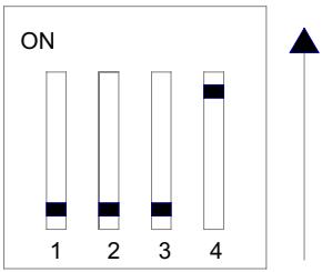
The SW1 switch is used to set the card ID. For example, if SW1 Pin 1 is set to ON and the others are OFF, the card index is 1. The index value can be from 0 to 15.
![ON\n1 2 3 4](.amp-304c-50m-00053-1000-10/7492267da6a647b67ef89cc0b4c418daf4cd50b5b575f49f984332b9b9d255b2.jpg)

<table><tr><td>Card ID</td><td>Switch Setting (ON=1)</td></tr><tr><td>0</td><td>0000</td></tr><tr><td>1</td><td>0001</td></tr><tr><td>2</td><td>0010</td></tr><tr><td>3</td><td>0011</td></tr><tr><td>4</td><td>0100</td></tr><tr><td>5</td><td>0101</td></tr><tr><td>6</td><td>0110</td></tr><tr><td>7</td><td>0111</td></tr><tr><td>8</td><td>1000</td></tr><tr><td>9</td><td>1001</td></tr><tr><td>10</td><td>1010</td></tr><tr><td>11</td><td>1011</td></tr><tr><td>12</td><td>1100</td></tr><tr><td>13</td><td>1101</td></tr><tr><td>14</td><td>1110</td></tr><tr><td>15</td><td>1111 (default)</td></tr></table>

Table 2-2: SW1 Card ID Selection

# 2.4.2 SW2 – End Limit Type Selection

The SW2 switch is used to set the type of end limit logic, which are Normally Open (NO) and Normally Closed (NC). For example, if the switch pin is set to "OFF", the type of end limit logic is Normally Open.

![ON\n1 2 3 4](.amp-304c-50m-00053-1000-10/e9916d7077f6f51d0aa1c1e773bd8332840d7c5054a321bf8bb0e444814b145f.jpg)

<table><tr><td>Axis #</td><td>SW2 Pin No.</td><td>NO (Default)</td><td>NC</td></tr><tr><td>0</td><td>1</td><td>OFF</td><td>ON</td></tr><tr><td>1</td><td>2</td><td>OFF</td><td>ON</td></tr><tr><td>2</td><td>3</td><td>OFF</td><td>ON</td></tr><tr><td>3</td><td>4</td><td>OFF</td><td>ON</td></tr></table>

Table 2-3: SW2 End Limit Type Selection

# 2.4.3 SW3 – DO Initial State Selection

The SW3 switch is used to set the initial DO state group setting. For example, if the SW3 Pin1 is set to "OFF", the initial states of "DO0 to DO3" are Inactive.

![ON\n1 2 3 4](.amp-304c-50m-00053-1000-10/f002cfd2a124394a736bd0d3f8bcc3773301096d1edb26f4ba74a9951d5426f7.jpg)

<table><tr><td>DO #</td><td>SW3 Pin No.</td><td>Inactive (Default)</td><td>Active</td></tr><tr><td>DO0 - DO3</td><td>1</td><td>OFF</td><td>ON</td></tr><tr><td>DO4 - DO7</td><td>2</td><td>OFF</td><td>ON</td></tr><tr><td>DO8 - DO11</td><td>3</td><td>OFF</td><td>ON</td></tr><tr><td>DO12 - DO15</td><td>4</td><td>OFF</td><td>ON</td></tr></table>

Table 2-4: SW3 DO Initial State Selection

# 2.5 Jumper Setting: Pulse Output Mode Selection

# 2.5.1 J1-J8 – Pulse Output Mode Selection

Jumpers J1-J8 are used to set the mode of pulse output signals. The output signal mode can either be differential line driver or single-ended output. Refer to Section 3.1 for detailed jumper settings.

<table><tr><td>J7 &amp; J8</td><td>Axis 0</td></tr><tr><td>J3 &amp; J4</td><td>Axis 1</td></tr><tr><td>J5 &amp; J6</td><td>Axis 2</td></tr><tr><td>J1 &amp; J2</td><td>Axis 3</td></tr></table>

![Based on the provided image, here is an accurate and concise description:\n\n**Blocks and Labels:**\n*   **J1**: A label at the top center of a rectangular connector outline.\n*   **1, 2, 3**: Numbers vertically aligned on the left side of the connector outline.\n*   **Differential (1-2) (default)**: Text on the far left.\n*   **Single-ended (2-3)**: Text below the previous text.\n*   **Black Squares with White Circles**: Inside the J1 outline, there are two large black squares. Each square contains two white circles. Below each black square is a smaller white circle.\n\n**Connections:**\n*   An arrow connects the text **'Differential (1-2) (default)'** to the pin labeled **1**.\n*   An arrow connects the text **'Single-ended (2-3)'** to the pin labeled **2**.](.amp-304c-50m-00053-1000-10/d0e6ed1651aeba71645c44be7a1d96df18d819ce8f114853819c5538a8eb6894.jpg)

# 2.5.2 CN3 – CMP Output Voltage Selection

The CN3 jumper is used to set the CMP output (dedicated) voltage, which are Open Collector Output (default), VDD (5V) and E24V.

<table><tr><td>1</td><td>4</td><td>7</td><td>10</td></tr><tr><td></td><td></td><td></td><td></td></tr><tr><td></td><td></td><td></td><td></td></tr><tr><td></td><td></td><td></td><td></td></tr><tr><td>3</td><td>6</td><td>9</td><td>12</td></tr></table>

<table><tr><td>CMP #</td><td>Open Collector (Default)</td><td>VDD (5V)</td><td>E24V</td></tr><tr><td colspan="4">Close Breaks Between</td></tr><tr><td>0</td><td>N/A</td><td>1 and 2</td><td>2 and 3</td></tr><tr><td>1</td><td>N/A</td><td>4 and 5</td><td>5 and 6</td></tr><tr><td>2</td><td>N/A</td><td>7 and 8</td><td>8 and 9</td></tr><tr><td>3</td><td>N/A</td><td>10 and 11</td><td>11 and 12</td></tr></table>

Table 2-5: CN3 – CMP Output Voltage Selection

# 2.6 Connector Pin Assignments

# 2.6.1 CN1 – Extended TTL DIO

![2\n40\n1\n39](.amp-304c-50m-00053-1000-10/f83a6baf8e92c39a7d28369af41d28dd3e2c2b73692101aee02fa895cde10512.jpg)

<table><tr><td>No.</td><td>Name</td><td>I/O</td><td>Function</td><td>No.</td><td>Name</td><td>I/O</td><td>Function</td></tr><tr><td>1</td><td>TDI0/T-LTC0</td><td>I</td><td>3.3V/5V TTL Input</td><td>2</td><td>TDI1/T-LTC1</td><td>I</td><td>3.3V/5V TTL Input</td></tr><tr><td>3</td><td>TDI2/T-LTC2</td><td>I</td><td>3.3V/5V TTL Input</td><td>4</td><td>TDI3/T-LTC3</td><td>I</td><td>3.3V/5V TTL Input</td></tr><tr><td>5</td><td>TDI4</td><td>I</td><td>3.3V/5V TTL Input</td><td>6</td><td>TDI5</td><td>I</td><td>3.3V/5V TTL Input</td></tr><tr><td>7</td><td>TDI6</td><td>I</td><td>3.3V/5V TTL Input</td><td>8</td><td>TDI7</td><td>I</td><td>3.3V/5V TTL Input</td></tr><tr><td>9</td><td>TDI8</td><td>I</td><td>3.3V/5V TTL Input</td><td>10</td><td>TDI9</td><td>I</td><td>3.3V/5V TTL Input</td></tr><tr><td>11</td><td>TDI10</td><td>I</td><td>3.3V/5V TTL Input</td><td>12</td><td>TDI11</td><td>I</td><td>3.3V/5V TTL Input</td></tr><tr><td>13</td><td>TDI12</td><td>I</td><td>3.3V/5V TTL Input</td><td>14</td><td>TDI13</td><td>I</td><td>3.3V/5V TTL Input</td></tr><tr><td>15</td><td>TDI14</td><td>I</td><td>3.3V/5V TTL Input</td><td>16</td><td>TDI15</td><td>I</td><td>3.3V/5V TTL Input</td></tr><tr><td>17</td><td>D5V</td><td>O</td><td>Digital Power +5V</td><td>18</td><td>D5V</td><td>O</td><td>Digital Power +5V</td></tr><tr><td>19</td><td>GND</td><td>--</td><td>Digital GND</td><td>20</td><td>GND</td><td>--</td><td>Digital GND</td></tr><tr><td>21</td><td>TDO0</td><td>O</td><td>5V TTL Output</td><td>22</td><td>TDO1</td><td>O</td><td>5V TTL Output</td></tr><tr><td>23</td><td>TDO2/T-CMP2</td><td>O</td><td>5V TTL Output</td><td>24</td><td>TDO3/T-CMP3</td><td>O</td><td>5V TTL Output</td></tr><tr><td>25</td><td>TDO4</td><td>O</td><td>5V TTL Output</td><td>26</td><td>TDO5</td><td>O</td><td>5V TTL Output</td></tr><tr><td>27</td><td>TDO6</td><td>O</td><td>5V TTL Output</td><td>28</td><td>TDO7</td><td>O</td><td>5V TTL Output</td></tr><tr><td>29</td><td>TDO8</td><td>O</td><td>5V TTL Output</td><td>30</td><td>TDO9</td><td>O</td><td>5V TTL Output</td></tr><tr><td>31</td><td>TDO10</td><td>O</td><td>5V TTL Output</td><td>32</td><td>TDO11</td><td>O</td><td>5V TTL Output</td></tr><tr><td>33</td><td>TDO12</td><td>O</td><td>5V TTL Output</td><td>34</td><td>TDO13</td><td>O</td><td>5V TTL Output</td></tr><tr><td>35</td><td>TDO14</td><td>O</td><td>5V TTL Output</td><td>36</td><td>----</td><td>--</td><td>Reserved</td></tr><tr><td>37</td><td>GND</td><td>--</td><td>Digital GND</td><td>38</td><td>----</td><td>--</td><td>Reserved</td></tr><tr><td>39</td><td>----</td><td>--</td><td>Reserved</td><td>40</td><td>----</td><td>--</td><td>Reserved</td></tr></table>

Table 2-6: CN3 Extended TTL DIO

![The image displays a simple icon featuring a white document with a folded top-right corner and faint horizontal lines. A large, bold, red checkmark is superimposed over the center of the document.](.amp-304c-50m-00053-1000-10/f54638ab660ddc9b66dfb352a8dc2bda2d0701de8df27363a8558983f7cd607f.jpg)
NOTE:

1. Maximum D5V output current = 0.5A.
2. TDI0-3, configured as TTL LTC Input if not used.
3. TDO0-3, configured as TTL CMP Output if not used.

# 2.6.2 CN2 – AMP-304C Main Connector

34
1
![Front view of a dual-pin electrical connector with terminal connectors (no text or symbols visible)](.amp-304c-50m-00053-1000-10/0bd2dd291eadba51d54d78d669efee576b8d67ceb8abbf4105684446bc2d82f3.jpg)

68
35

<table><tr><td>No.</td><td>Name</td><td>I/O</td><td>Function</td><td>No.</td><td>Name</td><td>I/O</td><td>Function</td></tr><tr><td>1</td><td>OUT0+</td><td>O</td><td>Pulse Signal +</td><td>35</td><td>OUT2+</td><td>O</td><td>Pulse Signal +</td></tr><tr><td>2</td><td>OUT0-</td><td>O</td><td>Pulse Signal -</td><td>36</td><td>OUT2-</td><td>O</td><td>Pulse Signal -</td></tr><tr><td>3</td><td>DIR0+</td><td>O</td><td>Direction Signal +</td><td>37</td><td>DIR2+</td><td>O</td><td>Direction Signal +</td></tr><tr><td>4</td><td>DIR0-</td><td>O</td><td>Direction Signal -</td><td>38</td><td>DIR2-</td><td>O</td><td>Direction Signal -</td></tr><tr><td>5</td><td>OUT1+</td><td>O</td><td>Pulse Signal +</td><td>39</td><td>OUT3+</td><td>O</td><td>Pulse Signal +</td></tr><tr><td>6</td><td>OUT1-</td><td>O</td><td>Pulse Signal -</td><td>40</td><td>OUT3-</td><td>O</td><td>Pulse Signal -</td></tr><tr><td>7</td><td>DIR1+</td><td>O</td><td>Direction Signal +</td><td>41</td><td>DIR3+</td><td>O</td><td>Direction Signal +</td></tr><tr><td>8</td><td>DIR1-</td><td>O</td><td>Direction Signal -</td><td>42</td><td>DIR3-</td><td>O</td><td>Direction Signal -</td></tr><tr><td>9</td><td>DGND</td><td>--</td><td>Digital GND</td><td>43</td><td>ALM2</td><td>I</td><td>Servo Alarm Signal</td></tr><tr><td>10</td><td>ALM0</td><td>I</td><td>Servo Alarm Signal</td><td>44</td><td>ALM3</td><td>I</td><td>Servo Alarm Signal</td></tr><tr><td>11</td><td>ALM1</td><td>I</td><td>Servo Alarm Signal</td><td>45</td><td>SVON0 /DO8</td><td>O</td><td>Servo On Signal / Digital Output</td></tr><tr><td>12</td><td>CMP4 /DO0</td><td>O</td><td>Position Comparison Trigger / Digital Output</td><td>46</td><td>SVON1 /DO9</td><td>O</td><td>Servo On Signal / Digital Output</td></tr></table>

Table 2-7: CN2 AMP-304C Main Connector

<table><tr><td>No.</td><td>Name</td><td>I/O</td><td>Function</td><td>No.</td><td>Name</td><td>I/O</td><td>Function</td></tr><tr><td>13</td><td>CMP5/DO1</td><td>O</td><td>Position Comparison Trigger / Digital Output</td><td>47</td><td>SVON2/DO10</td><td>O</td><td>Servo On Signal / Digital Output</td></tr><tr><td>14</td><td>CMP6/DO2</td><td>O</td><td>Position Comparison Trigger / Digital Output</td><td>48</td><td>SVON3/DO11</td><td>O</td><td>Servo On Signal / Digital Output</td></tr><tr><td>15</td><td>CMP7/DO3</td><td>O</td><td>Position Comparison Trigger / Digital Output</td><td>49</td><td>ERC0/DO12</td><td>O</td><td>Servo Deviation Counter Clear Signal / Digital Output</td></tr><tr><td>16</td><td>CMP8/DO4</td><td>O</td><td>Position Comparison Trigger / Digital Output</td><td>50</td><td>ERC1/DO13</td><td>O</td><td>Servo Deviation Counter Clear Signal / Digital Output</td></tr><tr><td>17</td><td>CMP9/DO5</td><td>O</td><td>Position Comparison Trigger / Digital Output</td><td>51</td><td>ERC2/DO14</td><td>O</td><td>Servo Deviation Counter Clear Signal / Digital Output</td></tr><tr><td>18</td><td>CMP10/DO6</td><td>O</td><td>Position Comparison Trigger / Digital Output</td><td>52</td><td>ERC3/DO15</td><td>O</td><td>Servo Deviation Counter Clear Signal / Digital Output</td></tr><tr><td>19</td><td>CMP11/DO7</td><td>O</td><td>Position Comparison Trigger / Digital Output</td><td>53</td><td>RDY0/DI8</td><td>I</td><td>Servo Ready Signal / Digital Input</td></tr><tr><td>20</td><td>EMG0/DI0</td><td>I</td><td>Emergency Stop Signal / Digital Input</td><td>54</td><td>RDY1/DI9</td><td>I</td><td>Servo Ready Signal / Digital Input</td></tr><tr><td>21</td><td>EMG1/DI1</td><td>I</td><td>Emergency Stop Signal / Digital Input</td><td>55</td><td>RDY2/DI10</td><td>I</td><td>Servo Ready Signal / Digital Input</td></tr><tr><td>22</td><td>EMG2/DI2</td><td>I</td><td>Emergency Stop Signal / Digital Input</td><td>56</td><td>RDY3/DI11</td><td>I</td><td>Servo Ready Signal / Digital Input</td></tr><tr><td>23</td><td>EMG3/DI3</td><td>I</td><td>Emergency Stop / Digital Input</td><td>57</td><td>INP0/DI12</td><td>I</td><td>Servo In-Position Signal / Digital Input</td></tr></table>

Table 2-7: CN2 AMP-304C Main Connector

<table><tr><td>No.</td><td>Name</td><td>I/O</td><td>Function</td><td>No.</td><td>Name</td><td>I/O</td><td>Function</td></tr><tr><td>24</td><td>Multi0 /DI4</td><td>I</td><td>Multi-Function* / Digital Input</td><td>58</td><td>INP1 /DI13</td><td>I</td><td>Servo In-Position Signal / Digital Input</td></tr><tr><td>25</td><td>Multi1 /DI5</td><td>I</td><td>Multi-Function* / Digital Input</td><td>59</td><td>EGND</td><td>--</td><td>External Power GND</td></tr><tr><td>26</td><td>Multi2 /DI6</td><td>I</td><td>Multi-Function* / Digital Input</td><td>60</td><td>INP2 /DI14</td><td>I</td><td>Servo In-Position Signal / Digital Input</td></tr><tr><td>27</td><td>Multi3 /DI7</td><td>I</td><td>Multi-Function* / Digital Input</td><td>61</td><td>INP3 /DI15</td><td>I</td><td>Servo In-Position Signal / Digital Input</td></tr><tr><td>28</td><td>PEL0</td><td>I</td><td>Positive End Limit Signal</td><td>62</td><td>PEL2</td><td>I</td><td>Positive End Limit Signal</td></tr><tr><td>29</td><td>MEL0</td><td>I</td><td>Negative End Limit Signal</td><td>63</td><td>MEL2</td><td>I</td><td>Negative End Limit Signal</td></tr><tr><td>30</td><td>ORG0</td><td>I</td><td>Origin Position Signal</td><td>64</td><td>ORG2</td><td>I</td><td>Origin Position Signal</td></tr><tr><td>31</td><td>PEL1</td><td>I</td><td>Positive End Limit Signal</td><td>65</td><td>PEL3</td><td>I</td><td>Positive End Limit Signal</td></tr><tr><td>32</td><td>MEL1</td><td>I</td><td>Negative End Limit Signal</td><td>66</td><td>MEL3</td><td>I</td><td>Negative End Limit Signal</td></tr><tr><td>33</td><td>ORG1</td><td>I</td><td>Origin Position Signal</td><td>67</td><td>ORG3</td><td>I</td><td>Origin Position Signal</td></tr><tr><td>34</td><td>EGND</td><td>--</td><td>External Power GND</td><td>68</td><td>E24V</td><td>I</td><td>External +24V Power Input</td></tr></table>

Table 2-7: CN2 AMP-304C Main Connector

![The image displays a white icon resembling a piece of paper or document with a folded top-right corner and faint horizontal lines. Superimposed over the document is a large, bold red checkmark.](.amp-304c-50m-00053-1000-10/5b40759753c30d41f67b5ccc48cd188f92c9c724fe76cba5265d4e61b97d1b04.jpg)
NOTE:

▶ DGND, used for OUT+/- and DIR+/- signals.
▶ EGND, used for others IO signals.
▶ DO0-7, configured as CMP Output if not used.
▶ DI0-3, configured as EMG Input if not used.
▶ DI4-7, configured as Multi-function if not used.

▷ SD: Direction Ramping-down Point Detection Signal.

▷ S-LTC: Position Latch Input Signal (Slow).

▷ PCS: Target Position Override Signal.

▷ CLR: Reset Counter Signal.

▶ SVON/ERC, configured as DO if not used.
▶ RDY/INP, configured as DI if not used.

# 2.6.3 CN4 – Encoder Feedback, LTC, and CMP Signals
![2\n40\n1\n39](.amp-304c-50m-00053-1000-10/14edaca75a4112c9f7f5a87bcfc4e9563cff1b7b4b5ed39be97037398477fde3.jpg)

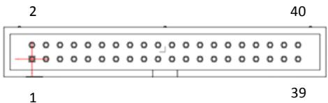
<table><tr><td>No.</td><td>Name</td><td>I/O</td><td>Function</td><td>No.</td><td>Name</td><td>I/O</td><td>Function</td></tr><tr><td>1</td><td>CMP3</td><td>O</td><td>Position Comparison Trigger</td><td>2</td><td>LTC3</td><td>I</td><td>Position Latch</td></tr><tr><td>3</td><td>CMP2</td><td>O</td><td>Position Comparison Trigger</td><td>4</td><td>LTC2</td><td>I</td><td>Position Latch</td></tr><tr><td>5</td><td>CMP1</td><td>O</td><td>Position Comparison Trigger</td><td>6</td><td>LTC1</td><td>I</td><td>Position Latch</td></tr><tr><td>7</td><td>CMP0</td><td>O</td><td>Position Comparison Trigger</td><td>8</td><td>LTC0</td><td>I</td><td>Position Latch</td></tr></table>

Table 2-8: CN4 Encoder Feedback, LTC, and CMP Signals

<table><tr><td>No.</td><td>Name</td><td>I/O</td><td>Function</td><td>No.</td><td>Name</td><td>I/O</td><td>Function</td></tr><tr><td>9</td><td>EGND</td><td>--</td><td>External Power GND</td><td>10</td><td>VDD</td><td>O</td><td>+5V Power Output</td></tr><tr><td>11</td><td>EZ3-</td><td>I</td><td>Encoder Z-phase-</td><td>12</td><td>EZ3+</td><td>I</td><td>Encoder Z-phase+</td></tr><tr><td>13</td><td>EB3-</td><td>I</td><td>Encoder B-phase-</td><td>14</td><td>EB3+</td><td>I</td><td>Encoder B-phase+</td></tr><tr><td>15</td><td>EA3-</td><td>I</td><td>Encoder A-phase-</td><td>16</td><td>EA3+</td><td>I</td><td>Encoder A-phase+</td></tr><tr><td>17</td><td>EZ2-</td><td>I</td><td>Encoder Z-phase-</td><td>18</td><td>EZ2+</td><td>I</td><td>Encoder Z-phase+</td></tr><tr><td>19</td><td>EB2-</td><td>I</td><td>Encoder B-phase-</td><td>20</td><td>EB2+</td><td>I</td><td>Encoder B-phase+</td></tr><tr><td>21</td><td>EA2-</td><td>I</td><td>Encoder A-phase-</td><td>22</td><td>EA2+</td><td>I</td><td>Encoder A-phase+</td></tr><tr><td>23</td><td>DGND</td><td>--</td><td>Digital GND</td><td>24</td><td>DGND</td><td>--</td><td>Digital GND</td></tr><tr><td>25</td><td>EZ1-</td><td>I</td><td>Encoder Z-phase-</td><td>26</td><td>EZ1+</td><td>I</td><td>Encoder Z-phase+</td></tr><tr><td>27</td><td>EB1-</td><td>I</td><td>Encoder B-phase-</td><td>28</td><td>EB1+</td><td>I</td><td>Encoder B-phase+</td></tr><tr><td>29</td><td>EA1-</td><td>I</td><td>Encoder A-phase-</td><td>30</td><td>EA1+</td><td>I</td><td>Encoder A-phase+</td></tr><tr><td>31</td><td>EZ0-</td><td>I</td><td>Encoder Z-phase-</td><td>32</td><td>EZ0+</td><td>I</td><td>Encoder Z-phase+</td></tr><tr><td>33</td><td>EB0-</td><td>I</td><td>Encoder B-phase-</td><td>34</td><td>EB0+</td><td>I</td><td>Encoder B-phase+</td></tr><tr><td>35</td><td>EA0-</td><td>I</td><td>Encoder A-phase-</td><td>36</td><td>EA0+</td><td>I</td><td>Encoder A-phase+</td></tr><tr><td>37</td><td>DGND</td><td>--</td><td>Digital GND</td><td>38</td><td>----</td><td>--</td><td>Reserved</td></tr><tr><td>39</td><td>----</td><td>--</td><td>Reserved</td><td>40</td><td>----</td><td>--</td><td>Reserved</td></tr></table>

Table 2-8: CN4 Encoder Feedback, LTC, and CMP Signals

![The image displays a simple graphic icon of a white document or piece of paper. The paper has a folded top-left corner and faint grey horizontal lines running across it, suggesting text or ruled paper. Superimposed over the document is a large, bold red check mark that slants upwards from left to right, indicating approval or completion.](.amp-304c-50m-00053-1000-10/0d85e876f711f51e83572deee8f0ea74235abeaa526c9f4480cf31d510196406.jpg)
NOTE:

1. VDD: Generated from E24V in CN2.
2. VDD/EGND: for CMP and LTC signals.
3. Digital GND: for Encoder signals.

# 2.6.4 CN5 – Manual Pulser Input Signals

![The image displays a technical diagram featuring the numbers '6' at the top left and '1' at the top right. Below these numbers is a horizontal rectangular frame consisting of an outer double-lined border and an inner single-lined border. Inside the inner rectangle is a horizontal row of six circular elements. The first five elements from the left are solid black dots. The sixth element, located on the far right, appears as a black ring surrounding a white center (or a white circle with a black dot). There are thin red lines near the rightmost circle; a vertical red line descends from the upper right area, and a horizontal red line extends from the right edge towards the left, seemingly indicating the components of the rightmost circle.](.amp-304c-50m-00053-1000-10/9b9a4f2042e2883e20489ab66e8d4dd62fb0319cc824ca297162773f2361b262.jpg)

<table><tr><td>No.</td><td>Name</td><td>I/O</td><td>Function</td></tr><tr><td>1</td><td>VDD</td><td>O</td><td>+5V Power Output</td></tr><tr><td>2</td><td>PA+</td><td>I</td><td>Pulser A-phase+ Input</td></tr><tr><td>3</td><td>PA-</td><td>I</td><td>Pulser A-phase- Input</td></tr><tr><td>4</td><td>PB+</td><td>I</td><td>Pulser B-phase+ Input</td></tr><tr><td>5</td><td>PB-</td><td>I</td><td>Pulser B-phase- Input</td></tr><tr><td>6</td><td>EGND</td><td>-</td><td>External Power GND</td></tr></table>

Table 2-9: CN5 Manual Pulser Input Signals

![The image displays a square icon representing a document. It features a white sheet of paper with a folded top-right corner and faint grey horizontal lines. A large, bold red checkmark is superimposed over the document. The entire graphic is enclosed within a black border.](.amp-304c-50m-00053-1000-10/6618e0a0c9af8be1414b0d47c9b1383501bf9e736f97f6b5859c75ab044ced38.jpg)
NOTE:

VDD: Generated from E24V in CN2.

This page intentionally left blank.

# 3 Signal Connections

Signal connections of all I/O's are described in this chapter. Refer to the contents of this chapter before wiring any cables between the AMP-304C and any motor drivers.

This chapter contains the following sections:

Section 3.1: Pulse Output Signals

Section 3.2: Encoder Feedback Input Signal

Section 3.3: Motion I/O Interface Signal

Section 3.4: GPIO Interface Signal

Section 3.5: Other I/O Interface Signals

# 3.1 Pulse Output Signals

There are 4 axis pulse output signals on the AMP-304C, each supporting up to 9.99 MHz output frequency. For each axis, two pairs of OUT and DIR signals are used to transmit the pulse train and to indicate the direction. In this section, the electrical characteristics of the OUT and DIR signals are detailed. Each signal consists of a pair of differential signals. For example, OUT2 consists of OUT2+ and OUT2- signals. The following table shows all pulse output signals on CN2.

<table><tr><td>Max. Axes</td><td>4</td></tr><tr><td>Pulse Output Frequency</td><td>Up to 9.99 MHz</td></tr><tr><td>Pulse Output Mode</td><td>CW/CCW, OUT/DIR, AB phases</td></tr><tr><td>Pulse Output Type</td><td>Differential / Single-End</td></tr></table>

<table><tr><td>Axis #</td><td>CN2 Pin No.</td><td>Signal Name</td><td>Description</td></tr><tr><td rowspan="4">0</td><td>1</td><td>OUT0+</td><td>Pulse Signal +</td></tr><tr><td>2</td><td>OUT0-</td><td>Pulse Signal -</td></tr><tr><td>3</td><td>DIR0+</td><td>Direction Signal +</td></tr><tr><td>4</td><td>DIR0-</td><td>Direction Signal -</td></tr><tr><td rowspan="4">1</td><td>5</td><td>OUT1+</td><td>Pulse Signal +</td></tr><tr><td>6</td><td>OUT1-</td><td>Pulse Signal -</td></tr><tr><td>7</td><td>DIR1+</td><td>Direction Signal +</td></tr><tr><td>8</td><td>DIR1-</td><td>Direction Signal -</td></tr><tr><td rowspan="4">2</td><td>35</td><td>OUT2+</td><td>Pulse Signal +</td></tr><tr><td>36</td><td>OUT2-</td><td>Pulse Signal -</td></tr><tr><td>37</td><td>DIR2+</td><td>Direction Signal +</td></tr><tr><td>38</td><td>DIR2-</td><td>Direction Signal -</td></tr><tr><td rowspan="4">3</td><td>39</td><td>OUT3+</td><td>Pulse Signal +</td></tr><tr><td>40</td><td>OUT3-</td><td>Pulse Signal -</td></tr><tr><td>41</td><td>DIR3+</td><td>Direction Signal +</td></tr><tr><td>42</td><td>DIR3-</td><td>Direction Signal -</td></tr></table>

Table 3-1: Pulse Output Signals

The output of the signals can be configured by jumpers as either Single-Ended or Differential Line Driver output. Users can select the output mode either by closing breaks between 1 and 2, or 2 and 3 of jumpers J1-J8 as follows:

![The image displays a connector diagram labeled **J1** at the top right. Below the label are two identical rectangular blocks representing the connector. The left block has three vertical pin numbers labeled **1**, **2**, and **3** to its left. Inside the block is a black square with two white dots and a white circle outline at the bottom.\n\nThere are two text labels with arrows pointing to the connector:\n*   **Differential (1-2) (default)** points via an arrow to pin **1**.\n*   **Single-ended (2-3)** points via an arrow to pin **3**.](.amp-304c-50m-00053-1000-10/e25c7806ab076c4359c48c8bde3802308b1e6d9c5518a651ceb4aefd07c50e59.jpg)

<table><tr><td>Axis #</td><td>Signal Name</td><td>Jumper</td><td>Differential Line Driver Output</td><td>Single-Ended Output</td></tr><tr><td rowspan="2">0</td><td>OUT0</td><td>J8</td><td rowspan="8">Close breaks between 1 and 2</td><td rowspan="8">Close breaks between 2 and 3</td></tr><tr><td>DIR0</td><td>J7</td></tr><tr><td rowspan="2">1</td><td>OUT1</td><td>J4</td></tr><tr><td>DIR1</td><td>J3</td></tr><tr><td rowspan="2">2</td><td>OUT2</td><td>J5</td></tr><tr><td>DIR2</td><td>J6</td></tr><tr><td rowspan="2">3</td><td>OUT3</td><td>J1</td></tr><tr><td>DIR3</td><td>J2</td></tr></table>

The default setting of OUT and DIR is set to differential line driver mode. The following wiring diagram is for OUT and DIR signals on the 4 axes.

![Based on the provided image, here is the description of the flowchart/block diagram:\n\n**Blocks:**\n*   **FPGA**: A square block on the far left.\n*   **Differential Line Driver**: A rectangular block in the center.\n*   **Connector**: A rectangular block on the right.\n*   **Power/Signal Header**: A small vertical component with three pins labeled **3**, **2**, and **1**.\n*   **Power Source**: Labeled **D5V** at the top right.\n*   **Ground Symbols**: Two downward-pointing triangles connected to the bottom of the 'Differential Line Driver' and the 'Connector'.\n*   **Arrow**: A hollow arrow pointing to the right at the bottom right corner.\n\n**Connections:**\n*   **FPGA** connects to the **Differential Line Driver**.\n*   From the **Differential Line Driver**, an upper signal line labeled **OUT+_ / DIR_+** connects to the small pin header.\n    *   Pin **3** of the header connects to **D5V**.\n    *   Pins **2** and **1** of the header connect to the signal line.\n    *   From this header, a line labeled **OUT+ / DIR+** continues to the **Connector**.\n*   From the **Differential Line Driver**, a lower signal line labeled **OUT- / DIR-** connects directly to the **Connector**.](.amp-304c-50m-00053-1000-10/47ce6fdd30adcbdeee7193d98de23837b72acd6bfad63ad478f81caeb48af8d6.jpg)

![The image displays a digital icon representing a document or file. It features a white sheet of paper with a folded top-left corner and faint horizontal lines running across it. A large, thick, red checkmark is superimposed over the document, slanting upwards from left to right.](.amp-304c-50m-00053-1000-10/950caf06392a835fccbd6f2df59544aa5b7419f69ea408771f62b2c7411946ae.jpg)
NOTE:

If the pulse output is set to Single-Ended output mode, OUT- and DIR- are used to transmit CW and CCW signals. The sink current must not exceed 20mA on the OUT- and DIR- pins.

# 3.2 Encoder Feedback Input Signal

The AMP-304C provides 4 encoder feedback input channels each with up to 4MHz and EA, EB, and EZ signals. Each group of EA, EB, and EZ signals contains a pair of differential signals (e.g. the EA signal contains EA+ and EA-).

A 32-bit counter for each encoder feedback input axis and two kinds of decoder modes (CW/CCW, 1x/2x/4x AB Phase) are available. For more information, see the APS Function Library User Manual.

<table><tr><td>Axis #</td><td>CN4 Pin No.</td><td>Signal Name</td><td>CN4 Pin No.</td><td>Signal Name</td></tr><tr><td rowspan="3">0</td><td>36</td><td>EA0+</td><td>35</td><td>EA0-</td></tr><tr><td>34</td><td>EB0+</td><td>33</td><td>EB0-</td></tr><tr><td>32</td><td>EZ0+</td><td>31</td><td>EZ0-</td></tr><tr><td rowspan="3">1</td><td>30</td><td>EA1+</td><td>29</td><td>EA1-</td></tr><tr><td>28</td><td>EB1+</td><td>27</td><td>EB1-</td></tr><tr><td>26</td><td>EZ1+</td><td>25</td><td>EZ1-</td></tr><tr><td rowspan="3">2</td><td>22</td><td>EA2+</td><td>21</td><td>EA2-</td></tr><tr><td>20</td><td>EB2+</td><td>19</td><td>EB2-</td></tr><tr><td>18</td><td>EZ2+</td><td>17</td><td>EZ2-</td></tr><tr><td rowspan="3">3</td><td>16</td><td>EA3+</td><td>15</td><td>EA3-</td></tr><tr><td>14</td><td>EB3+</td><td>13</td><td>EB3-</td></tr><tr><td>12</td><td>EZ3+</td><td>11</td><td>EZ3-</td></tr></table>

![Based on the provided block diagram, here is a description of the blocks and connections:\n\n**Blocks:**\n*   **Connector**: Located on the far left.\n*   **Differential Line Receiver**: Located in the center.\n*   **Schmitt Trigger**: Located to the right of the receiver.\n*   **Motion Chip & FPGA**: Located on the far right.\n\n**Connections and Components:**\n*   An arrow points into the **Connector** block.\n*   Two red signal lines exit the **Connector**:\n    *   The top line is labeled **EA+ / EB+ / EZ+**.\n    *   The bottom line is labeled **EA- / EB- / EZ-**.\n*   A resistor labeled **120** connects the top and bottom lines in parallel immediately after the connector.\n*   Both lines pass through resistors labeled **1K**.\n*   After the 1K resistors, there are three capacitors labeled **22pF** connected to ground (indicated by downward-pointing triangle symbols).\n*   The signal lines continue from the capacitor node into the **Differential Line Receiver**.\n*   A single line connects the **Differential Line Receiver** to the **Schmitt Trigger**.\n*   A single line connects the **Schmitt Trigger** to the **Motion Chip & FPGA**.](.amp-304c-50m-00053-1000-10/84b4f42a123f7ce02af28ac66b2418397c997eed04149105cd1a73211fde3849.jpg)

# 3.3 Motion I/O Interface Signal

# 3.3.1 Emergency Stop Input (EMG)

The AMP-304C provides an EMG signal, common with DI. If one of the EMG signals is triggered, all motion control commands will be stopped immediately. Another way to stop operation of each motor immediately is by transmitting an external EMG signal via the DIN-304C to a servo or stepper motor driver. Refer to the DIN-304C User's Manual for more details.

<table><tr><td>Axis #</td><td>CN2 Pin No.</td><td>Signal Name</td></tr><tr><td>0</td><td>20</td><td>EMG0</td></tr><tr><td>1</td><td>21</td><td>EMG1</td></tr><tr><td>2</td><td>22</td><td>EMG2</td></tr><tr><td>3</td><td>23</td><td>EMG3</td></tr></table>

![The image displays a circuit diagram with the following labeled blocks and connections:\n\n**Labeled Blocks and Components:**\n*   **Connector**: A block on the far left.\n*   **Schmitt Trigger**: A block in the middle-right.\n*   **FPGA**: A block on the far right.\n*   **Blue-bordered box**: Contains schematic symbols resembling transistors/diodes.\n*   **Resistors**: One labeled **3.3K** and a vertical one near the top.\n\n**Labels on Lines/Nets:**\n*   **E24V**: Label at a node on the top wire.\n*   **EMG**: Label on the bottom wire.\n*   **D3.3V**: Label at the top power rail.\n\n**Connections:**\n1.  An arrow points into the left side of the **Connector** block.\n2.  From the **Connector**, a top wire emerges and is labeled **E24V**. This line connects to a resistor labeled **3.3K**.\n3.  From the **Connector**, a bottom wire emerges labeled **EMG**.\n4.  Both the output of the **3.3K** resistor and the **EMG** line connect to the input side of the component inside the blue-bordered box.\n5.  The top output of the blue-bordered box connects to a junction point.\n6.  From this junction point, a vertical resistor connects upward to the **D3.3V** label.\n7.  From the same junction point, a line extends to the right, connecting to the **Schmitt Trigger** block.\n8.  The bottom output of the blue-bordered box connects to a ground symbol.\n9.  The **Schmitt Trigger** block connects to the **FPGA** block.](.amp-304c-50m-00053-1000-10/3020791330d344ac5b13d748eec635ca8e7468191b5ceacfd1498b4c57ea9d6d.jpg)

# 3.3.2 Mechanical Signal Input

The AMP-304C provides some dedicated input pins for mechanical signals such as original position signal (ORG), direction end limit signals (PEL/MEL), and direction ramping-down point detection signals (SD).

# 3.3.2.1 Origin Position Signal (ORG)

The AMP-304C provides one original or home signal for each axis. This signal is used for defining the zero position of this axis. The logic of this signal must be set properly before performing the home procedure.

<table><tr><td>Axis #</td><td>CN2 Pin No.</td><td>Signal Name</td></tr><tr><td>0</td><td>30</td><td>ORG0</td></tr><tr><td>1</td><td>33</td><td>ORG1</td></tr><tr><td>2</td><td>64</td><td>ORG2</td></tr><tr><td>3</td><td>67</td><td>ORG3</td></tr></table>

The input circuit of the ORG signals is shown below. Usually, a limit switch is used to indicate the origin on one axis. The specifications of the limit switch should have a contact capacity of +24V at 10mA minimum. An internal filter circuit is used to filter out any high frequency spikes, which may cause errors in the operation.

![This diagram shows a signal processing circuit.\n\n**Blocks:**\n*   **Connector** (Leftmost box)\n*   **Schmitt Trigger** (Middle-right box)\n*   **Motion Chip** (Rightmost box)\n*   A blue rectangular block containing optocoupler symbols (LEDs and a phototransistor) located centrally.\n\n**Connections and Labels:**\n1.  An arrow points toward the **Connector** block.\n2.  A line labeled **E24V** exits the **Connector**, passes through a resistor labeled **3.3K**, and enters the left side of the blue optocoupler block.\n3.  A red line labeled **ORG** exits the **Connector** and enters the bottom input of the blue optocoupler block.\n4.  The output of the blue optocoupler block connects to a pull-up resistor leading to a terminal labeled **D3.3V**.\n5.  The output of the blue optocoupler block also connects to a ground symbol (inverted triangle).\n6.  The signal line from the junction of the blue block and the pull-up resistor connects to the **Schmitt Trigger** block.\n7.  The **Schmitt Trigger** block connects to the **Motion Chip** block.](.amp-304c-50m-00053-1000-10/66aeca10510d83f97443bc60043a92c7668cdbef048734fadbef1e9514440401.jpg)

When the motion controller is operated in the home return mode, the ORG signal is used to inhibit the Pulse Output Signals.

# 3.3.2.2 Direction End Limit Signal (PEL / MEL)

The end-limit switches are usually installed on both ends of an axis. The positive EL must be installed at the positive position of the axis. If they are installed reversely, the protection will be invalid. These two signals are for safety, which can prevent a machine from crashing when missing an operation.

The AMP-304C provides two direction end limit signals, PEL and MEL, for each axis. PEL indicates the end limit signal is in the positive direction and MEL indicates the end limit signal is in the negative direction.

<table><tr><td>Axis #</td><td>CN2 Pin No.</td><td>Signal Name</td><td>CN2 Pin No.</td><td>Signal Name</td></tr><tr><td>0</td><td>28</td><td>PEL0</td><td>29</td><td>MEL0</td></tr><tr><td>1</td><td>31</td><td>PEL1</td><td>32</td><td>MEL1</td></tr><tr><td>2</td><td>62</td><td>PEL2</td><td>63</td><td>MEL2</td></tr><tr><td>3</td><td>65</td><td>PEL3</td><td>66</td><td>MEL3</td></tr></table>

The external limit switch should have a contact capacity of +24V at 10mA minimum. The EL logical can be configured via switch.

![Based on the provided image, here is the description of the flowchart/block diagram:\n\n**Labeled Blocks:**\n*   **Connector**: A large square block on the far left.\n*   **Schmitt Trigger**: A square block on the right.\n*   **Motion Chip**: A square block on the far right.\n*   There is a central unlabelled blue rectangular block containing electronic symbols (diodes and a transistor).\n\n**Connections:**\n1.  **Input**: An arrow points into the **Connector**.\n2.  **From Connector to Central Block**:\n    *   A top wire labeled **E24V** passes through a resistor labeled **3.3K** and connects to the top input of the central blue block.\n    *   A bottom wire labeled **PEL / MEL** connects to the bottom input of the central blue block.\n3.  **From Central Block to Schmitt Trigger**:\n    *   The output of the central blue block (the transistor symbol) connects to a signal line.\n    *   This signal line connects to the input of the **Schmitt Trigger**.\n    *   A resistor connects this signal line to a power source labeled **D3.3V**.\n    *   The emitter of the transistor in the blue block connects to ground (indicated by a triangle symbol).\n4.  **From Schmitt Trigger to Motion Chip**: A line connects the **Schmitt Trigger** block directly to the **Motion Chip** block.](.amp-304c-50m-00053-1000-10/22e51861cfbcb00c06c5d6fd217d09467834baa5570161c6825f43a6a28b6505.jpg)

# 3.3.2.3 Direction Ramping-down Point Detection Signal (SD)

The AMP-304C provides one slow-down function through SD signal input for each axis. SD indicates both positive and negative directions. For more information and settings, see the APS Function Library User's Manual.

<table><tr><td>Axis #</td><td>CN2 Pin No.</td><td>Signal Name</td></tr><tr><td>0</td><td>24</td><td>SD0</td></tr><tr><td>1</td><td>25</td><td>SD1</td></tr><tr><td>2</td><td>26</td><td>SD2</td></tr><tr><td>3</td><td>27</td><td>SD3</td></tr></table>

![The diagram shows a signal processing circuit with the following components and connections:\n\n1.  **Connector**: An arrow points into a block labeled **Connector**.\n2.  **Top Path**: A wire labeled **E24V** exits the top of the **Connector**, passes through a resistor labeled **3.3K**, and connects to the top input of a blue rectangular box (containing an optocoupler symbol).\n3.  **Bottom Path**: A wire labeled **SD** exits the bottom of the **Connector** and connects to the bottom input of the same blue rectangular box.\n4.  **Blue Box Outputs**:\n    *   The top output pin connects to a junction. From this junction, one path goes up through a resistor to a point labeled **D3.3V**. The other path goes to the right to a block labeled **Schmitt Trigger**.\n    *   The bottom output pin connects to a ground symbol.\n5.  **Final Stage**: The **Schmitt Trigger** block connects to a block labeled **FPGA**.](.amp-304c-50m-00053-1000-10/3c93b59fda6107fd48faaf80fd9164c194eaabf47e74c765e0abb0cc732f95ea.jpg)

# 3.3.3 Servo Interface IO

# 3.3.3.1 Servo-ON Output Signal (SVON)

The AMP-304C provides one servo on output signal, SVON, to enable servo drivers for each axis. For more information and settings, see the APS Function Library User's Manual.

SVON output signals can be configured as General-Purpose Digital Output signals if not used.

<table><tr><td>Axis #</td><td>CN2 Pin No.</td><td>Signal Name</td></tr><tr><td>0</td><td>45</td><td>SVON0</td></tr><tr><td>1</td><td>46</td><td>SVON1</td></tr><tr><td>2</td><td>47</td><td>SVON2</td></tr><tr><td>3</td><td>48</td><td>SVON3</td></tr></table>

![The diagram shows a signal path flowing from left to right:\n\n1.  A box labeled **FPGA** connects to a box labeled **Digital Isolator**.\n2.  The **Digital Isolator** connects to the terminal labeled **G** of a circular component.\n3.  This circular component has three terminals labeled **D**, **G**, and **S**.\n4.  The terminal labeled **D** connects upward to a red line labeled **SVON**, which then connects to a box labeled **Connector**.\n5.  The terminal labeled **S** connects downward to a red arrow pointing to the label **EGND**.](.amp-304c-50m-00053-1000-10/5a4b053b0a6922c71190f55eb3dd671058b7c8d9c43b0905a833079cb70c1c5c.jpg)

# 3.3.3.2 Servo Deviation Counter Clear Output Signal (ERC)

The AMP-304C provides one deviation counter clear function through ERC for each axis, which can be a pulse or a LEVEL signal output. The output logic and pulse width can be changed using software. For more information and settings, see the APS Function Library User's Manual.

ERC output signals can be configured as General-Purpose Digital Output signals if not used.

<table><tr><td>Axis #</td><td>CN2 Pin No.</td><td>Signal Name</td></tr><tr><td>0</td><td>49</td><td>ERC0</td></tr><tr><td>1</td><td>50</td><td>ERC1</td></tr><tr><td>2</td><td>51</td><td>ERC2</td></tr><tr><td>3</td><td>52</td><td>ERC3</td></tr></table>

![Based on the provided image, here is the description of the flowchart and its connections:\n\n**Labeled Blocks and Components:**\n*   **FPGA** (square box on the left)\n*   **Digital Isolator** (square box in the center)\n*   A circular component symbol with internal arrows, labeled with **G** (left), **D** (top right), and **S** (bottom right).\n*   **Connector** (square box on the right)\n\n**Connections:**\n*   A line connects **FPGA** to **Digital Isolator**.\n*   A line connects **Digital Isolator** to the **G** label on the circular component.\n*   A red line labeled **ERC** connects the **D** label of the circular component to the **Connector**.\n*   A red arrow points downward from the **S** label of the circular component to the text **EGND**.\n*   A right-pointing arrow is located below the **Connector** block.](.amp-304c-50m-00053-1000-10/1bf723f740a57a199c8eb2781314b9331113e1544fa5121f386c5b557911d92c.jpg)

# 3.3.3.3 Servo Alarm Input Signal (ALM)

The AMP-304C provides one servo alarm input signal, ALM, for each axis. The alarm signal is sent by servo drivers. If the ALM signal is triggered, motion of an axis stops immediately, or will decelerate and stop. The input logic can be selected using software. For more information and settings, see the APS Function Library User's Manual..

<table><tr><td>Axis #</td><td>CN2 Pin No.</td><td>Signal Name</td></tr><tr><td>0</td><td>10</td><td>ALM0</td></tr><tr><td>1</td><td>11</td><td>ALM1</td></tr><tr><td>2</td><td>43</td><td>ALM2</td></tr><tr><td>3</td><td>44</td><td>ALM3</td></tr></table>

![Based on the provided block diagram, here is the accurate description of the labeled blocks and their connections:\n\n**Labeled Blocks:**\n*   **Connector** (Left)\n*   **Motion Chip** (Right)\n*   (Central Block: An optocoupler enclosed in a blue box)\n\n**Connections:**\n*   An arrow points towards the **Connector** block.\n*   From the top terminal of the **Connector**, a line connects to a test point labeled **E24V**. This point connects to a resistor labeled **3.3K**, which then connects to the anodes of the two parallel input LEDs inside the central blue box.\n*   From the bottom terminal of the **Connector**, a line labeled **ALM** connects to the cathodes of the two parallel input LEDs inside the central blue box.\n*   Inside the blue box, the collector of the output phototransistor connects to a junction node.\n*   This junction node connects to the **Motion Chip**.\n*   The junction node also connects to a resistor, which connects upwards to a terminal labeled **D3.3V**.\n*   The emitter of the output phototransistor connects to a ground symbol.](.amp-304c-50m-00053-1000-10/9f369e63b719012ef878ad2c40e8f3dd45d78247c76ca49c7d3392c8a1ec03fb.jpg)

# 3.3.3.4 Servo Ready Input Signal (RDY)

The AMP-304C provides one servo ready input signal, RDY, for each axis, which is used to receive the ready signal from a servo driver. If RDY is enabled, the servo driver is ready to receive the pulse command from the AMP-304C. The input logic can be changed using software. For more information and settings, see the APS Function Library User's Manual.

RDY input signals can be configured as General-Purpose Digital Input signals if not used

<table><tr><td>Axis #</td><td>CN2 Pin No.</td><td>Signal Name</td></tr><tr><td>0</td><td>53</td><td>RDY0</td></tr><tr><td>1</td><td>54</td><td>RDY1</td></tr><tr><td>2</td><td>55</td><td>RDY2</td></tr><tr><td>3</td><td>56</td><td>RDY3</td></tr></table>

![Based on the provided image, here is an accurate and concise description of the flowchart/block diagram:\n\n**Blocks and Labels:**\n*   **Connector**: A large rectangular block on the left.\n*   **Blue Rectangular Component**: A component in the center containing symbols for a diode, an LED, and a phototransistor.\n*   **Schmitt Trigger**: A rectangular block to the right.\n*   **FPGA**: A rectangular block on the far right.\n*   **Text Labels**: 'E24V', '3.3K', 'RDY', 'D3.3V'.\n\n**Connections:**\n*   An arrow points into the **Connector**.\n*   From the **Connector**, a top line connects to a node labeled **E24V**, which then passes through a resistor labeled **3.3K** to the top input terminal of the blue rectangular component.\n*   From the **Connector**, a bottom line labeled **RDY** connects to the bottom-left input terminal of the blue rectangular component.\n*   A voltage source labeled **D3.3V** connects via a resistor to the top terminal of the blue rectangular component (the same node connected to the 3.3K resistor).\n*   This top terminal also serves as the output connection to the **Schmitt Trigger**.\n*   The bottom-right terminal of the blue rectangular component connects to a ground symbol.\n*   The **Schmitt Trigger** connects to the **FPGA**.](.amp-304c-50m-00053-1000-10/0b9231a5f44d230d0f658401f9028cd975a6984a47fea7a4d585c00c7e69580f.jpg)

# 3.3.3.5 Servo In-Position Input Signal (INP)

The AMP-304C provides one in-position input signal, INP, for each axis. It is used to check the position complete signal, which is from the servo driver if the position mode is set. The input logic can be changed using software. For more information and settings, see the APS Function Library User's Manual.

INP input signals can be configured as General-Purpose Digital Input signals if not used.

<table><tr><td>Axis #</td><td>CN2 Pin No.</td><td>Signal Name</td></tr><tr><td>0</td><td>57</td><td>INP0</td></tr><tr><td>1</td><td>58</td><td>INP1</td></tr><tr><td>2</td><td>60</td><td>INP2</td></tr><tr><td>3</td><td>61</td><td>INP3</td></tr></table>

![Based on the provided circuit diagram, here is an accurate description of the blocks and connections:\n\n**Labeled Blocks:**\n*   **Connector**: A square box on the left side.\n*   **Schmitt Trigger**: A square box in the middle-right section.\n*   **FPGA**: A square box on the far right.\n*   There is also a central blue rectangular block containing electronic symbols (diodes and a transistor), likely an optocoupler.\n\n**Connections and Labels:**\n*   **Signal Flow**: A large white arrow points from left to right, indicating the direction of signal flow.\n*   **Input Side (Left to Center)**:\n    *   From the **Connector**, a top wire connects to a point labeled **E24V**. This line continues through a resistor labeled **3.3K** to the top input of the blue box.\n    *   From the **Connector**, a bottom wire labeled **INP** (in red text) connects to the bottom input of the blue box.\n*   **Output Side (Center to Right)**:\n    *   The top output of the blue box connects to a junction point.\n    *   This junction connects to a resistor that goes up to a point labeled **D3.3V**.\n    *   This junction also connects to the input of the **Schmitt Trigger**.\n    *   The bottom output of the blue box connects to a ground symbol (triangle). Visually, the bottom input wire (**INP**) and the bottom output wire appear to share a common bottom rail connected to Ground.\n*   **Final Stage**: The output of the **Schmitt Trigger** connects to the **FPGA**.](.amp-304c-50m-00053-1000-10/f8819b9806cc27fc9f2e71df12d587b035caf9d2f83ba308dae3c5c85f5adf93.jpg)

# 3.4 GPIO Interface Signal

The AMP-304C provides a 32-channel onboard optically isolated GPIO (DI/DO) and a 32-channel extended TTL GPIO (TDI/TDO).

<table><tr><td rowspan="2">GPIO Onboard</td><td rowspan="2">Main Connector CN2</td><td>16-ch Optically Isolated DI</td></tr><tr><td>16-ch Optically Isolated DO</td></tr><tr><td rowspan="2">GPIO Extended</td><td rowspan="2">Extend Connector CN1</td><td>16-ch Non-isolated TTL DI</td></tr><tr><td>16-ch Non-isolated TTL DO</td></tr></table>

# 3.4.1 32-Channel Onboard Isolated GPIO (DI/DO)

<table><tr><td>CN2 Pin No.</td><td>Signal Name</td><td>CN2 Pin No.</td><td>Signal Name</td></tr><tr><td>20</td><td>DI0 / EMG0</td><td>12</td><td>DO0 / CMP4</td></tr><tr><td>21</td><td>DI1 / EMG1</td><td>13</td><td>DO1 / CMP5</td></tr><tr><td>22</td><td>DI2 / EMG2</td><td>14</td><td>DO2 / CMP6</td></tr><tr><td>23</td><td>DI3 / EMG3</td><td>15</td><td>DO3 / CMP7</td></tr><tr><td>24</td><td>DI4 / Multi0</td><td>16</td><td>DO4 / CMP8</td></tr><tr><td>25</td><td>DI5 / Multi1</td><td>17</td><td>DO5 / CMP9</td></tr><tr><td>26</td><td>DI6 / Multi2</td><td>18</td><td>DO6 / CMP10</td></tr><tr><td>27</td><td>DI7 / Multi3</td><td>19</td><td>DO7 / CMP11</td></tr><tr><td>53</td><td>DI8 / RDY0</td><td>45</td><td>DO8 / SVON0</td></tr><tr><td>54</td><td>DI9 / RDY1</td><td>46</td><td>DO9 / SVON1</td></tr><tr><td>55</td><td>DI10 / RDY2</td><td>47</td><td>DO10 / SVON2</td></tr><tr><td>56</td><td>DI11 / RDY3</td><td>48</td><td>DO11 / SVON3</td></tr><tr><td>57</td><td>DI12 / INP0</td><td>49</td><td>DO12 / ERC0</td></tr><tr><td>58</td><td>DI13 / INP1</td><td>50</td><td>DO13 / ERC1</td></tr><tr><td>60</td><td>DI14 / INP2</td><td>51</td><td>DO14 / ERC2</td></tr><tr><td>61</td><td>DI15 / INP3</td><td>52</td><td>DO15 / ERC3</td></tr></table>

Optically Isolated Digital Input:
![Based on the provided image, here is an accurate and concise description of the flowchart/block diagram:\n\n**Labeled Blocks:**\n*   **Connector**: A large rectangular block on the far left.\n*   **Schmitt Trigger**: A rectangular block in the middle-right.\n*   **FPGA**: A rectangular block on the far right.\n*   **Blue-bordered box**: A rectangular block with a blue outline containing diode and transistor symbols (an optocoupler).\n\n**Connections and Text:**\n*   A large arrow points into the **Connector**.\n*   From the top of the **Connector**, a wire leads to a node labeled **E24V**, then passes through a resistor labeled **3.3K** before entering the top input of the blue-bordered box.\n*   From the bottom of the **Connector**, a wire labeled **DI** (in red text) enters the bottom input of the blue-bordered box.\n*   The output side of the blue-bordered box connects to a pull-up resistor. The top of this resistor connects to a node labeled **D3.3V**.\n*   The junction between the blue-bordered box output and the pull-up resistor connects to the **Schmitt Trigger**.\n*   The bottom output of the blue-bordered box connects to a ground symbol.\n*   The **Schmitt Trigger** connects to the **FPGA**.](.amp-304c-50m-00053-1000-10/70fd7022140d2977f49e6292764ad1191acd89cf244acd4beb7db747e35b54ae.jpg)

Optically Isolated Digital Output:
![Based on the provided image, here is the accurate description of the blocks and connections:\n\n**Labeled Blocks and Components:**\n*   **FPGA**\n*   **Digital Isolator**\n*   **Connector**\n*   A circular component (symbolizing a MOSFET) with terminals labeled **G**, **D**, and **S**.\n*   **EGND** (Ground label)\n\n**Connections:**\n*   A line connects the **FPGA** block to the **Digital Isolator** block.\n*   A line connects the **Digital Isolator** block to the **G** terminal of the circular component.\n*   A red line labeled **DO** connects the **D** terminal of the circular component to the **Connector** block.\n*   A red line connects the **S** terminal of the circular component to the **EGND** ground symbol.](.amp-304c-50m-00053-1000-10/43d98af1412f182fbaadac0caca521b5bab754ac4031eccbde732411a7a876d3.jpg)

# 3.4.2 32-Channel Extended TTL GPIO (TDI/TDO)

<table><tr><td>CN1 Pin No.</td><td>Signal Name</td><td>CN1 Pin No.</td><td>Signal Name</td></tr><tr><td>1</td><td>TDI0</td><td>21</td><td>TDO0</td></tr><tr><td>2</td><td>TDI1</td><td>22</td><td>TDO1</td></tr><tr><td>3</td><td>TDI2</td><td>23</td><td>TDO2</td></tr><tr><td>4</td><td>TDI3</td><td>24</td><td>TDO3</td></tr><tr><td>5</td><td>TDI4</td><td>25</td><td>TDO4</td></tr><tr><td>6</td><td>TDI5</td><td>26</td><td>TDO5</td></tr><tr><td>7</td><td>TDI6</td><td>27</td><td>TDO6</td></tr><tr><td>8</td><td>TDI7</td><td>28</td><td>TDO7</td></tr><tr><td>9</td><td>TDI8</td><td>29</td><td>TDO8</td></tr><tr><td>10</td><td>TDI9</td><td>30</td><td>TDO9</td></tr><tr><td>11</td><td>TDI10</td><td>31</td><td>TDO10</td></tr><tr><td>12</td><td>TDI11</td><td>32</td><td>TDO11</td></tr><tr><td>13</td><td>TDI12</td><td>33</td><td>TDO12</td></tr><tr><td>14</td><td>TDI13</td><td>34</td><td>TDO13</td></tr><tr><td>15</td><td>TDI14</td><td>35</td><td>TDO14</td></tr><tr><td>16</td><td>TDI15</td><td>36</td><td>TDO15</td></tr></table>

Non-isolated TTL Digital Input:
![The flowchart features three rectangular blocks arranged horizontally:\n\n*   **Connector**\n*   **Schmitt Trigger**\n*   **FPGA**\n\n**Connections and Labels:**\n\n*   An arrow points into the left side of the **Connector**.\n*   A red line connects the right side of the **Connector** to the left side of the **Schmitt Trigger**. This line is labeled with the text '**5V / 3.3V TTL DI**' and the number '**33**'. A resistor symbol is drawn on this line.\n*   A red line connects the right side of the **Schmitt Trigger** to the left side of the **FPGA**.\n*   A red line extends from the bottom of the **Schmitt Trigger** down to a ground symbol.](.amp-304c-50m-00053-1000-10/53ce6ae8be8bbb6eacf993cdddc49e8cb4516a2f7b47f7788f2539bda167e86e.jpg)

Non-isolated TTL Digital Output:
![The diagram displays a signal processing chain with three labeled blocks and their connections:\n\n**Labeled Blocks:**\n*   **FPGA**\n*   **Buffer and Driver**\n*   **Connector**\n\n**Connections:**\n*   A line connects the right side of the **FPGA** block to the left side of the **Buffer and Driver** block.\n*   From the **Buffer and Driver** block, a line extends upward to a terminal labeled **D5V**.\n*   From the **Buffer and Driver** block, a line extends downward to a ground symbol.\n*   From the **Buffer and Driver** block, a line extends to the right, passing through a resistor labeled **33**, and connects to the left side of the **Connector** block. This signal path is labeled **5V TTL DO**.](.amp-304c-50m-00053-1000-10/246c7477c3729fda8f8c08f52e4b44187c62594b13c1497d16f30ed766bf4711.jpg)

# 3.5 Other I/O Interface Signals

# 3.5.1 Position Latch Input (LTC)

The AMP-304C provides 12-channel position latch trigger inputs.

▶ LTC: 4-channel dedicated and isolated input, up to 1MHz
▶ S-LTC: 4-channel isolated and common with DI, up to 10KHz (slower)
▶ T-LTC: 4-channel TTL and common with TDI, up to 1MHz

With encoder feedback input signals, a position latch function is available for each axis. Any 12-channel position latch input can be assigned to a latch source to trigger any axis by software. The AMP-304C provides 256 position latch buffer points for each axis. For more information, see the APS Function Library User's Manual.

<table><tr><td>CN4 Pin No.</td><td>Signal Name</td></tr><tr><td>8</td><td>LTC0</td></tr><tr><td>6</td><td>LTC1</td></tr><tr><td>4</td><td>LTC2</td></tr><tr><td>2</td><td>LTC3</td></tr></table>

<table><tr><td>CN2 Pin No.</td><td>Signal Name</td><td>CN3 Pin No.</td><td>Signal Name</td></tr><tr><td>24</td><td>S-LTC0</td><td>1</td><td>T-LTC0</td></tr><tr><td>25</td><td>S-LTC1</td><td>2</td><td>T-LTC1</td></tr><tr><td>26</td><td>S-LTC2</td><td>3</td><td>T-LTC2</td></tr><tr><td>27</td><td>S-LTC3</td><td>4</td><td>T-LTC3</td></tr></table>

![The image displays a white document icon with a folded top-right corner. Faint grey horizontal lines run across the page, resembling text. A large red checkmark is superimposed over the center of the document. There is no actual text present in the image.](.amp-304c-50m-00053-1000-10/c76f78447ccd7b9b4764fbd7aca256374a0cc53a97c169e179f1da9b8e32990d.jpg)
NOTE:

For S-LTC circuit diagram, see Section 3.4.1: 32-Channel Onboard Isolated GPIO (DI/DO).

For T-LTC circuit diagram, see Section 3.4.2: 32-Channel Extended TTL GPIO (TDI/TDO).

![Based on the provided circuit diagram, here is the accurate and concise description of the labeled blocks and their connections:\n\n**Labeled Blocks and Components:**\n*   **Connector**\n*   **Schmitt Trigger**\n*   **FPGA**\n*   Resistor labeled **330**\n*   Capacitor labeled **100pF**\n*   Optocoupler (indicated by the blue box)\n*   Unlabeled resistor connected to **D3.3V**\n\n**Connections:**\n*   A line labeled **LTC** extends from the **Connector** to the cathode (bottom terminal) of the optocoupler.\n*   **VDD** connects to one side of the **330** resistor.\n*   The other side of the **330** resistor connects to the anode (top terminal) of the optocoupler and one side of the **100pF** capacitor.\n*   The other side of the **100pF** capacitor connects to the **LTC** line.\n*   The collector (top terminal) of the optocoupler's phototransistor connects to a junction.\n*   This junction connects to the input of the **Schmitt Trigger** and one side of the unlabeled resistor.\n*   The other side of the unlabeled resistor connects to **D3.3V**.\n*   The emitter (bottom terminal) of the phototransistor connects to ground.\n*   The output of the **Schmitt Trigger** connects to the **FPGA**.](.amp-304c-50m-00053-1000-10/a95a9be933688afa28156b8f02dd5b437538ff673f7ffe51ff5deec5d71210b9.jpg)

# 3.5.2 Position Comparison Trigger Output (CMP)

The AMP-304C provides 16-channel position comparison trigger outputs.

▶ CMP 0-3: 4-channel dedicated and isolated output, up to 1MHz
▶ CMP 4-11: 8-channel isolated, common with DO, up to 1MHz
▶ T-CMP 0-3: 4-channel TTL, common with TDO, up to 1MHz

Voltage output selection is controlled by jumper in dedicated CMP outputs; see Section 2.5.2: CN3 – CMP Output Voltage Selection.

<table><tr><td>CN4 Pin No.</td><td>Signal Name</td></tr><tr><td>7</td><td>CMP0</td></tr><tr><td>5</td><td>CMP1</td></tr><tr><td>3</td><td>CMP2</td></tr><tr><td>1</td><td>CMP3</td></tr></table>

<table><tr><td>CN2 Pin No.</td><td>Signal Name</td><td>CN1 Pin No.</td><td>Signal Name</td></tr><tr><td></td><td></td><td></td><td></td></tr><tr><td>12</td><td>CMP4</td><td>21</td><td>T-CMP0</td></tr><tr><td>13</td><td>CMP5</td><td>22</td><td>T-CMP1</td></tr><tr><td>14</td><td>CMP6</td><td>23</td><td>T- CMP2</td></tr><tr><td>15</td><td>CMP7</td><td>24</td><td>T- CMP3</td></tr><tr><td>16</td><td>CMP8</td><td></td><td></td></tr><tr><td>17</td><td>CMP9</td><td></td><td></td></tr><tr><td>18</td><td>CMP10</td><td></td><td></td></tr></table>

![The image shows a white document icon featuring horizontal grey lines resembling lined paper. A large red checkmark is drawn diagonally across the center. The top right corner of the document is folded down.](.amp-304c-50m-00053-1000-10/41258b9886e66b6b29c305ae3b61106ea1f9a2a3b7288151f9996156261aa77f.jpg)
NOTE:

For CMP 4-11 circuit diagram, see Section 3.4.1:32-Channel Onboard Isolated GPIO (DI/DO).
For T-CMP 0-3 circuit diagram, see Section 3.4.2:32-Channel Extended TTL GPIO (TDI/TDO).

With encoder feedback input signals, a position comparison trigger function is available for each axis. Any 16-channel position comparison trigger output can be assigned as a pulse output mode with width configurable or a toggle output mode. The AMP-304C provides 256 position comparison buffer points for each axis, including Linear and Table comparison modes. Position-reusable is also available in Table comparison modes. For more information, see the APS Function Library User's Manual.

![Based on the provided circuit diagram, here is the accurate and concise description:\n\n**Labeled Blocks:**\n*   **FPGA**\n*   **Digital Isolator**\n*   **MOSFET** (labeled with terminals **D**, **G**, and **S**)\n*   **CN3** (a connector block with pins labeled **1**, **2**, and **3**)\n*   **Connector** (a box with an arrow pointing outward)\n\n**Connections:**\n*   The **FPGA** connects to the **Digital Isolator**.\n*   The **Digital Isolator** connects to the Gate (**G**) of the MOSFET.\n*   The Source (**S**) of the MOSFET connects to **EGND**.\n*   The Drain (**D**) of the MOSFET connects to a line labeled **CMP**.\n*   This **CMP** line connects to pin **2** of **CN3**.\n*   The **CMP** line continues from **CN3** to the **Connector** box.\n*   Pin **3** of **CN3** connects to a resistor labeled **4.7K**, which connects to **E24V**. (The label **CMP** is present near this connection).\n*   Pin **1** of **CN3** connects to a resistor labeled **330**, which connects to **VDD**. (The label **CMP** is present near this connection).](.amp-304c-50m-00053-1000-10/d21bae337cc24455fd9de500d0f7d022dfd020467280efb3fabded4849e0dac9.jpg)

# 3.5.3 Manual Pulser Input Signal (PA/PB)

The AMP-304C provides one set of manual pusler functions through PA/PB for all axes. CW/CCW and 1x/2x/4x AB Phase modes are supported for receiving external drive pulses. For more information, see the APS Function Library User's Manual.

<table><tr><td>CN5 Pin No.</td><td>Signal Name</td></tr><tr><td>2</td><td>PA+</td></tr><tr><td>3</td><td>PA-</td></tr><tr><td>4</td><td>PB+</td></tr><tr><td>5</td><td>PB-</td></tr></table>

![Connector\nPA+/PB+\n330\n100pF\nD3.3V\nMotion\nChip\nPA-/PB-](.amp-304c-50m-00053-1000-10/ca3e470f681eac10854faadd1054821e33c44e63e41b5d937adab1e248448c6b.jpg)

# 3.5.4 Multi-function Input Signals (DI/SD/S-LTC/PCS/CLR)

Multi-function input signals (DI/SD/S-LTC/PCS/CLR) are allocated through DI4-7.

For DI, see Section 3.4.1: 32-Channel Onboard Isolated GPIO (DI/DO).
▶ For SD, see Section 3.3.2.3: Direction Ramping-down Point Detection Signal (SD).
▶ For S-LTC, see Section 3.5.1: Position Latch Input (LTC).
▶ PCS is used to override a target position.
▶ CLR is used to reset a specified counter.

For more information, see the APS Function Library User's Manual.

<table><tr><td>Axis #</td><td>CN2 Pin No.</td><td>Signal Name</td></tr><tr><td>0</td><td>24</td><td>DI4 / SD0 / S-LTC0 / PCS0 / CLR0</td></tr><tr><td>1</td><td>25</td><td>DI5 / SD1 / S-LTC1 / PCS1 / CLR1</td></tr><tr><td>2</td><td>26</td><td>DI6 / SD2 / S-LTC2 / PCS2 / CLR2</td></tr><tr><td>3</td><td>27</td><td>DI7 / SD3 / S-LTC3 / PCS3 / CLR3</td></tr></table>

![The diagram illustrates a signal conditioning circuit with the following labeled blocks and connections:\n\n**Labeled Blocks and Components:**\n*   **Connector** (Left)\n*   **Schmitt Trigger** (Right)\n*   **FPGA** (Far Right)\n*   **Optocoupler** (Central blue-outlined box containing an LED and phototransistor)\n\n**Connections:**\n1.  **Input:** An arrow points into the left side of the **Connector**.\n2.  **Input Signal Path:**\n    *   The top wire from the **Connector** connects to a node labeled **E24V**, passes through a resistor labeled **3.3K**, and connects to the anode of the optocoupler.\n    *   The bottom wire from the **Connector**, labeled **CLR / PCS**, connects to the cathode of the optocoupler.\n3.  **Output Signal Path:**\n    *   The collector of the optocoupler connects to a junction point.\n    *   A resistor connects from the label **D3.3V** to this same junction point.\n    *   The junction connects to the input of the **Schmitt Trigger**.\n    *   The emitter of the optocoupler connects to a ground symbol.\n4.  **Final Output:** A line connects the output of the **Schmitt Trigger** directly to the input of the **FPGA**.](.amp-304c-50m-00053-1000-10/af79f8664611b9238c440734cb87879b3a9f7d788323286cad68243c30f6cff2.jpg)

# Important Safety Instructions

For user safety, please read and follow all instructions, Warnings, Cautions, and Notes marked in this manual and on the associated device before handling/operating the device, to avoid injury or damage.

▶ Read these safety instructions carefully.
- Keep the User’s Manual for future reference.
▶ Read the Specifications section of this manual for detailed information on the recommended operating environment.
The device can be operated at an ambient temperature of $45^{\circ}$ C with DC input, and $35^{\circ}$ C with adapter input.
It is recommended that the device be installed in Information Technology Rooms that are in accordance with Article 645 of the National Electrical Code and NFPA 75.

▶ To avoid electrical shock and/or damage to device:

▷ Keep device away from water or liquid sources.
▷ Keep device away from high heat or humidity.
▷ Keep device properly ventilated (do not block or cover ventilation openings).
▶ Always use recommended voltage and power source settings.
▶ Always install and operate device near an easily accessible electrical outlet.
▷ Secure the power cord (do not place any object on/over the power cord).
▶ Only install/attach and operate device on stable surfaces and/or recommended mountings.
The power cord must be connected to a socket or outlet with a ground connection.

▶ If the device will not be used for long periods of time, turn off and unplug from its power source.
▶ Never attempt to repair the device, which should only be serviced by qualified technical personnel using suitable tools.

▶ A Lithium-type battery may be provided for uninterrupted backup or emergency power.

![The image displays a yellow triangular warning sign with a thick black border. Inside the triangle is a large black exclamation mark. Below the triangle, the text 'CAUTION:' is printed in black capital letters.](.amp-304c-50m-00053-1000-10/ca612c4621fca6e999e23b525716c4eb719de7530d5dffcd2edfa2f264d4ec48.jpg)

Risk of explosion if battery is replaced with one of an incorrect type; please dispose of used batteries appropriately.

This equipment is not suitable for use in locations where children are likely to be present.
▶ The device must be serviced by authorized technicians when:

The power cord or plug is damaged
▷ Liquid has entered the device interior
The device has been exposed to high humidity and/or moisture
The device is not functioning or does not function according to the User's Manual
The device has been dropped and/or damaged and/or shows obvious signs of breakage

▶ Disconnect the power supply cord before loosening the thumbscrews and always fasten the thumbscrews with a screwdriver before starting the system up
It is recommended that the device be installed only in a server room or computer room where access is:

▷ Restricted to qualified service personnel or users familiar with restrictions applied to the location, reasons therefor, and any precautions required
▶ Only afforded by the use of a tool or lock and key, or other means of security, and controlled by the authority responsible for the location

![Warning sign depicting steam rising inside a yellow triangle, indicating hazardous or hazardous material.](.amp-304c-50m-00053-1000-10/6d18466ab383306e1b598239c5bf94cec10598bbd9339535a711830906b8cfe7.jpg)

# BURN HAZARD

Hot surface! Do not touch! Touching this surface could result in bodily injury. To reduce risk, allow the surface to cool before touching.

# Consignes de Sécurité Importante

S'il vous plaît prêter attention stricte à tous les avertissements et mises en garde figurant sur l'appareil, pour éviter des blessures ou des dommages.

▶ Lisez attentivement ces consignes de sécurité.
▶ Conservez le manuel de l'utilisateur pour pouvoir le consulter ultérieurement.
▶ Lisez la section Spécifications de ce manuel pour des informations détaillées sur l'environnement d'exploitation recommandé.
L'appareil peut être utilisé à une température ambiante de 45°C avec entrée CC pour les série MVP-61; 35°C avec entrée adaptateur pour la série MVP-61.
Il est recommandé d'installer l'appareil dans des salles de technologie de l'information conformes à l'article 645 du National Electrical Code et à la NFPA 75.

Pour éviter les chocs électriques et/ou d'endommager l'appareil:

▷ Tenez l'appareil à l'écart de toute source d'eau ou de liquide.
▷ Tenez l'appareil à l'écart d'une forte chaleur ou d'une humidité élevée.
▶ Maintenez l'appareil correctement ventilé (n'obstruer ou ne couvrez pas les ouvertures de ventilation).
Utilisez toujours les réglages de tension et de source d'alimentation recommandés.
Installez et utilisez toujours l'appareil près d'une prise de courant facilement accessible.
▷ Fixez le cordon d'alimentation (ne placez aucun objet sur le cordon d'alimentation).
Installez/fixez et utilisez l'appareil uniquement sur des surfaces stables et/ou sur les fixations recommandées.
▷ Le cordon d'alimentation doit être connecté à une prise ou à une prise de courant avec mise à la terre.

Si l'appareil ne doit pas être utilisé pendant de longues périodes, éteignez-le et débranchez-le de sa source d'alimentation
N'essayez jamais de réparer l'appareil, qui ne doit être réparé que par un personnel technique qualifié à l'aide d'outils appropriés
Une batterie de type Lithium peut être fournie pour une alimentation de secours ininterrompue ou d'urgence.

![The image displays a yellow triangular warning sign with a thick black border and an exclamation point in the center. Below the triangle, the word 'CAUTION:' is printed in bold black capital letters.](.amp-304c-50m-00053-1000-10/11a0175531503b6770243636b0e37c6ab293a38aadb7c7770992bbd62c2076c3.jpg)

ATTENTION: Risque d'explosion si la pile est remplacée par une autre de type incorrect. Veuillez jeter les piles usagées de façon appropriée.

Cet équipement ne convient pas à une utilisation dans des lieux pouvant accueillir des enfants.
L'appareil doit être entretenu par des techniciens agrees lorsque:
▶ Le cordon d'alimentation ou la prise est endommagé(e)
▶ Un liquide a pénétré à l'intérieur de l'appareil.
L'appareil a été exposé à une forte humidité et/ou de la buée.
L'appareil ne fonctionne pas ou ne fonctionne pas selon le manuel de l'utilisateur.
L'appareil est tombé et/ou a été endommagé et/ou présente des signes évidents de dommage.
Débranchez le cordon d'alimentation avant de desserrer les vis à oreilles et serrez toujours les vis à oreilles avec un tournevis avant de mettre le système en marche.
Il est recommandé d'installer l'appareil uniquement dans une salle de serveurs ou une salle informatique où l'accès est:

Réservé au personnel de service qualifié ou aux utilisateurs familiarisés avec les restrictions appliquées à l'emplacement, aux raisons de ces restrictions et toutes les précautions requises
▷ Uniquement autorisé par l'utilisation d'un outil, d'une serrure et d'une clé, ou d'un autre moyen de sécurité, et contrôlé par l'autorité responsable de l'emplacement.

![Warning sign depicting steam rising inside a yellow triangle, indicating caution or hazard.](.amp-304c-50m-00053-1000-10/b70da59ab478eeb1ab0f6fe855c7537961cc3a1c78993aec05fca6498bbd4ccf.jpg)

# RISQUE DE BRÛLURES

Partie chaude! Ne touchez pas cette surface, cela pourrait entraîner des blessures. Pour éviter tout danger, laissez la surface refroidir avant de la toucher.

This page intentionally left blank.

# Getting Service

Ask an Expert: http://askanexpert.adlinktech.com

# ADLINK Technology, Inc.

No. 66, Huaya 1st Rd., Guishan District

Taoyuan City 333411, Taiwan

Tel: +886-3-216-5088

Fax: +886-3-328-5706

Email: service@adlinktech.com

# Ampro ADLINK Technology, Inc.

6450 Via Del Oro

San Jose, CA 95119-1208, USA

Tel: +1-408-360-0200

Toll Free: +1-800-966-5200 (USA only)

Fax: +1-408-600-1189

Email: info@adlinktech.com

# ADLINK Technology (China) Co., Ltd.

300 Fang Chun Rd., Zhangjiang Hi-Tech Park

Pudong New Area, Shanghai, 201203 China

Tel: +86-21-5132-8988

Fax: +86-21-5132-3588

Email: market@adlinktech.com

# ADLINK Technology GmbH

Hans-Thoma-Straße 11

D-68163 Mannheim, Germany

Tel: +49-621-43214-0

Fax: +49-621 43214-30

Email: emea@adlinktech.com

Please visit the Contact page at www.adlinktech.com for information on how to contact the ADLINK regional office nearest you.
[🔗 Link to the original document](.amp-304c-50m-00053-1000-10/amp-304c-50m-00053-1000-10.pdf)
