# aTCA-3100 Series

# AdvancedTCA Base/Fabric Switch Blade

User's Manual

Manual Rev. 2.00

Revision Date: October 16, 2006

Part No: 50-1G002-2000

![The image features a black circle containing the white universal recycling symbol. The symbol consists of three arrows arranged in a triangular loop, with parallel lines near the arrowheads.](.atca-3100series-manual-3/e1186d91e69187a26e02459ecc1d825e802210f61956570901760263c8c4d2e9.jpg)
Recycled Paper

Copyright 2006 ADLINK TECHNOLOGY INC.

All Rights Reserved.

The information in this document is subject to change without prior notice in order to improve reliability, design, and function and does not represent a commitment on the part of the manufacturer.

In no event will the manufacturer be liable for direct, indirect, special, incidental, or consequential damages arising out of the use or inability to use the product or documentation, even if advised of the possibility of such damages.

This document contains proprietary information protected by copyright. All rights are reserved. No part of this manual may be reproduced by any mechanical, electronic, or other means in any form without prior written permission of the manufacturer.

# Trademarks

Product names mentioned herein are used for identification purposes only and may be trademarks and/or registered trademarks of their respective companies.

# Getting service from ADLINK

Customer satisfaction is our top priority. Contact us should you require any service or assistance.

# ADLINK TECHNOLOGY INC.

Web Site http://www.adlinktech.com

Sales & Service service@adlinktech.com

Telephone No. +886-2-82265877

Fax No. +886-2-82265717

Address 9F, No. 166, Jian Yi Road, Chungho City,

Taipei, 235 Taiwan

Please email or fax this completed service form for prompt and satisfactory service.

<table><tr><td colspan="2">Company Information</td></tr><tr><td>Company/Organization</td><td></td></tr><tr><td>Contact Person</td><td></td></tr><tr><td>E-mail Address</td><td></td></tr><tr><td>Address</td><td></td></tr><tr><td>Country</td><td></td></tr><tr><td>TEL</td><td>FAX:</td></tr><tr><td>Web Site</td><td></td></tr><tr><td colspan="2">Product Information</td></tr><tr><td>Product Model</td><td></td></tr><tr><td>Environment</td><td>OS:M/B: CPU:Chipset: BIOS:</td></tr></table>

Please give a detailed description of the problem(s):

# Table of Contents

# List of Tables...... iii

# List of Figures ...... v

# 1 Introduction ...... 1

1.1 Product overview .... 1
1.2 Features.... 2
1.3 Reference specifications.... 3
1.4 Block diagrams ...... 3

aTCA-3100 base switch blade 3
aTCA-3110/3120 fabric switch blade 4
80219 CPU sub-system block diagram 5

1.5 Functional Description 6

Control processor sub-system 6
Base interface 8
Fabric interface 9

1.6 Port slot mapping.... 11
Base switch channel mapping 11
1.7 Fabric Switch Channel Mapping 12
1.8 Front panel.... 13

aTCA-3100 13
aTCA-3110 14
aTCA-3120 15

1.9 Configuration switches.... 16

Switch 3 17
Switch 4 18
Switch 9 18

# 2 Installation 19

2.1 Installing the card.... 19

Connecting the serial cable 19
Accessing the aTCA-3100 Series card 20
Firmware boot sequence 21

# 3 Connector Pinouts 23

3.1 Zone 1 connector (P10)....23
3.2 Zone 2 connectors.... 24

J20 24

J21 25
J22 25
J23 26
J24 26

3.3 Zone 3 connectors 27

J2 Rear I/O connector 27

J1 Rear I/O connector 28

DDR SODIMM connector 29

80219 JTAG debug connector 32

RJ-11 serial port connector 32

RJ-45 gigabit Ethernet ports 33

3.4 Electrical specifications.... 34

Absolute maximum ratings 34

Input characteristics 34

# Warranty Policy 35

# List of Tables

Table 1-1: Base switch channel mapping 11

Table 1-2: Fabric switch channel mapping ...... 12

Table 1-3: Switch 3 description 17

Table 1-4: Options selection for SW3 17

Table 1-5: Switch 4 description 18

Table 1-6: Switch 9 description 18

Table 3-1: Zone 1 connector P10 23

Table 3-2: J20 connector 24

Table 3-3: J21 connector 25

Table 3-4: J22 connector 25

Table 3-5: J23 connector 26

Table 3-6: J24 connector 26

Table 3-7: J2 RTM connector 27

Table 3-8: J1 RTM Connector 28

Table 3-9: DDR SODIMM connector 29

Table 3-10: 80219 JTAG debug connector 32

Table 3-11: RJ-11 serial port connector 32

Table 3-12: RJ-45 Gigabit Ethernet ports 33

Table 3-13: Absolute maximum ratings 34

Table 3-14: Input characteristics ...... 34

# List of Figures

Figure 1-1: aTCA-3100 card-level block diagram 3

Figure 1-2: aTCA-3110/3120 card-level block diagram 4

Figure 1-3: CPU sub-system block diagram 5

Figure 1-4: IPMC block diagram 8

Figure 1-5: Dual-star base interface logical slot routing....9

Figure 1-6: Dual-star fabric interface logical routing slot.... 10

Figure 1-7: aTCA-3100 front panel 13

Figure 1-8: aTCA-3110 front panel 14

Figure 1-9: aTCA-3120 front panel 15

Figure 1-10: aTCA-3100 Series switch locations.... 16

# 1 Introduction

# 1.1 Product overview

This aTCA-3100 Series is an AdvancedTCA switch blade supporting base and fabric Interfaces for ATCA shelves up to 14 slots (2 hub slots and 12 node slots). The board provides fabric switching of 1000Base-X gigabit Ethernet on each fabric slot.

The aTCA-3100 Series is based on the Vitesse $^{®}$ VSC7310 switch silicon and the Intel $^{®}$ 80219 600 MHz XScale $^{®}$ I/O processor. The basic aTCA-3100 base switch blade features a 24-port 10/100/1000BASE-T link including 12 node slots, 8 front panel egress RJ-45 ports, 2 ShMC ports, 1 inter-switch port, and 1 control plane CPU access port.

In addition to the aTCA-3100 features, the fabric aTCA-3110 switch blade features a 24-port 1000BASE-BX link including 14 PIGMG 3.1 option 1-compliant node slots, 2 front panel egress ports, and 8 reserved ports from Rear Transition Module I/O.

On top of the aTCA-3110 feature set, the aTCA-3120 highlights a fabric switch blade with 10GbE uplink support with an additional 10 gigabit Ethernet XFP uplink port.

Linux-based operating system runs on Intel $^{®}$ 80219 processor to provide a complete development platform for the management of Layer 2/3 packet switching and routing, plus sophisticated standards such as IEEE 802.1d Spanning Tree Protocol (STP), IEEE 802.1p Quality-of-Service (QoS), IEEE 802.1Q 4096 VLANs, IEEE 802.3ad Link aggregation, Port Mirroring, and DHCP services.

# 1.2 Features

# ▶ Control plane processor

▷ Intel $^{®}$ 80219 XScale $^{®}$ I/O processor at 600 MHz
▷ Configuration port (Serial)
▶ Two 10/100/1000 Ethernet maintenance ports, one Ethernet, one ShMC
▷ 64-bit, 66 MHz PCI bus
▷ DDR200 SDRAM (up to 1 GB)
▶ Up to 128 MB of flash program storage
▷ Dual-flash boot capability
▷ IPM controller

# ▶ Base interface

▷ 1000Base-TX gigabit Ethernet
▷ Layer 3 switching
▷ Base interface support for 14 node slots
▷ Base interface support for redundant switch card
▷ Full-speed non-blocking switching (port-to-port)
▶ Eight (8) front-panel GbE ports (base interface access)
▷ Support for dual-Ethernet shelf manager control (ShMC port)

# ▶ Fabric interface (aTCA-3110 and aTCA-3120 only)

▷ 1000Base-X gigabit Ethernet, Option 1, Link Type 2
▷ Layer 3 switching
▶ Supports 14-slot shelf
▷ Fabric interface - one GbE ports per channel (13 ports)
▷ Full-speed, non-blocking switching (port-to-port)
▶ Two front panel GbE ports (fabric access)
▶ Rear I/O GbE ports (fabric access, RTM required)

# 1.3 Reference specifications

▷ PICMG 3.0 R2.0 ECN001 ATCA Core Specification
▷ PICMG 3.1 R1.0 Option1 Ethernet Over PICMG 3.0

# 1.4 Block diagrams

# 1.4.1 aTCA-3100 base switch blade

Figure 1-1 shows the major components and sub-systems of the aTCA-3100 blade.
![This block diagram illustrates a system architecture involving power management, a microprocessor subsystem, a gigabit Ethernet switch, and various interface connections.\n\n**Labeled Blocks:**\n*   **IPM Controller Sub-System**\n*   **ATCA Power Module**\n*   **ATCA Power (Zone 1)**\n*   **Maintenance Port (10/100/1000)** (containing an **RJ45** block)\n*   **RJ11** (labeled **Serial Debug Port**)\n*   **80219 µP Sub-System** (containing a **Dual GigE** block)\n*   **Base Switch** (containing **VSC 7310 24 Port GigE Switch**)\n*   **Front Panel** (label)\n*   **Quad PHY** (four blocks on the left side, four blocks on the right side)\n*   **RJ45** (groups of ports under the Front Panel label)\n*   **Base Interface Access Ports** (label)\n*   **PICMG 3.0 Base Interface (Zone 2)** (containing channel labels: **Ch 1, ShMC1**, **Ch 1, ShMC2**, **Ch 2, Hub**, **Ch 3** through **Ch 15**)\n\n**Connections:**\n*   **IPM Controller Sub-System** connects to **ATCA Power Module** via **Power Control**.\n*   **IPM Controller Sub-System** connects to **ATCA Power (Zone 1)** via two lines labeled **IPMB**.\n*   **ATCA Power (Zone 1)** connects to **ATCA Power Module** via two lines labeled **-48V** and two lines labeled **IPMB** (arrows point towards the module).\n*   **IPM Controller Sub-System** connects to **80219 µP Sub-System** via **Serial IPM Payload Port** and **Status Lines (GPIO)**.\n*   **IPM Controller Sub-System** receives **Hot Swap Control/Board Monitor** (arrow points left).\n*   **80219 µP Sub-System** receives a connection from **Maintenance Port (10/100/1000)** via **Dual GigE** (purple line).\n*   **80219 µP Sub-System** receives a connection from **RJ11** via **Serial Debug Port** (red arrow).\n*   **80219 µP Sub-System** connects to **Base Switch** via **32 Bit, 66 MHz Bus** (blue arrow).\n*   **Base Switch** connects to the left-side **Quad PHY** blocks, which in turn connect to the **RJ45** blocks under **Front Panel** (pink arrows point left).\n*   **Base Switch** connects to the right-side **Quad PHY** blocks, which connect to **PICMG 3.0 Base Interface (Zone 2)** (pink arrows point right).\n*   **PICMG 3.0 Base Interface (Zone 2)** lists channels **Ch 1, ShMC1**, **Ch 1, ShMC2**, **Ch 2, Hub**, **Ch 3** through **Ch 14**, and **Ch 15** (with a circle-X symbol).](.atca-3100series-manual-3/279de8d556b0fbf928273f0ba6b3375da123280632560d21eb99f3965d82a95b.jpg)

Figure 1-1: aTCA-3100 card-level block diagram

# 1.4.2 aTCA-3110/3120 fabric switch blade

Figure 1-2 shows the major components and sub-systems of the aTCA-3110 and aTCA-3120 blades.
![**Top Section (Power & Control)**\n*   **Blocks:** 'IPM Controller Sub-System', 'ATCA Power Module', 'ATCA Power (Zone 1)'.\n*   **Connections:**\n    *   'Hot Swap Control/ Board Monitor' connects to 'IPM Controller Sub-System'.\n    *   'IPM Controller Sub-System' connects to 'ATCA Power Module' (labeled 'Power Control').\n    *   'ATCA Power Module' connects to 'ATCA Power (Zone 1)' (labeled '-48V').\n    *   'IPM Controller Sub-System' connects to 'ATCA Power (Zone 1)' (labeled 'IPMB').\n\n**Central Processing & Bus**\n*   **Blocks:** '80219 uP Sub-System' (contains 'Dual GbE'), 'Base Switch' (labeled 'VSC 7310 24 Port GbE Switch').\n*   **Connections:**\n    *   'IPM Controller Sub-System' connects to '80219 uP Sub-System' (labeled 'Serial IPMI Payload Port').\n    *   '80219 uP Sub-System' connects to 'IPM Controller Sub-System' (labeled 'Status Lines (GPIO)').\n    *   '80219 uP Sub-System' connects to 'Base Switch' (labeled '32 Bit, 66 MHz Bus').\n\n**Front Panel Inputs**\n*   **Maintenance Port:** Labeled 'Maintenance Port (10/100/1000)'. Contains an 'RJ45' block connecting to '80219 uP Sub-System' and an 'RJ11' block (labeled 'Serial Debug Port') connecting to '80219 uP Sub-System'.\n*   **Base Interface Access Ports:** A group of 'RJ45' blocks connects to 'Quad PHY' blocks, which connect to the 'Base Switch'.\n*   **Fabric Access Ports:** 'RJ45' blocks connect to a 'Quad PHY' block, which connects to the 'Fabric Switch'.\n*   **10 Gbps Uplink:** A dashed box labeled '10 Gbps Uplink' contains '10 GbE Optional' and '88C2012 XGMII - XFI'. '10 GbE Optional' connects to '88C2012 XGMII - XFI' (labeled 'XFI'). '88C2012 XGMII - XFI' connects to the 'Fabric Switch' (labeled 'XGMII'). Text 'aTCA-3120 only' points to this section.\n\n**Switching & Zone 2 Interfaces**\n*   **Base Switch:** Connects to multiple 'Quad PHY' blocks. These connect to 'PICMG 3.0 Base Interface (Zone 2)' with channel labels: 'Ch 1, ShMC1', 'Ch 1, ShMC2', 'Ch 2, Hub', 'Ch 3', 'Ch 4', 'Ch 5', 'Ch 6', 'Ch 7', 'Ch 9', 'Ch 10', 'Ch 11', 'Ch 12', 'Ch 13', 'Ch 14', and 'Ch 15'.\n*   **Fabric Switch:** Labeled 'Fabric Switch' and 'VSC7310 Non Blocking Switch (Level 3 Switching, 24 Ports)'. Connects to 'Quad PHY' blocks which connect to 'PICMG 3.0 Fabric Interface (Zone 2)' with channel labels: 'Ch 1', 'Ch 2', 'Ch 3', 'Ch 4', 'Ch 5', 'Ch 6', 'Ch 7', 'Ch 8', 'Ch 9', 'Ch 10', 'Ch 11', 'Ch 12', 'Ch 13', 'Ch 14'. Additionally, '8 RTM Fabric Ports (RTM)' connects to the bottom of 'PICMG 3.0 Fabric Interface (Zone 2)'.](.atca-3100series-manual-3/16f78c26f65a3166a4a2096d686fc67527acf84c8236a9b85055c3a069becff6.jpg)

Figure 1-2: aTCA-3110/3120 card-level block diagram

The switch connects to the ATCA channels in such a way as to provide one GbE port for each ATCA channel.

Two of the fabric switch ports are allocated for front panel external access. Eight additional ports are routed to a rear RTM access connector.

An optional 10 gigabit uplink port on aTCA-3120 provides support for a high-speed external link to the shelf.

# 1.4.3 80219 CPU sub-system block diagram

Figure 1-3 shows the control processor sub-system.
![**Labeled Blocks:**\n\n*   **SODIMM DDR200** (Image of a memory module)\n*   **Flash EPROM 64MB** (Two separate blocks)\n*   **80219 I/O Processor (Xscale)**\n*   **82546 Dual GbE**\n*   **DUAL UART 16C552**\n\n**Connections and Labels:**\n\n*   **Redundant Flash Image, Dual Boot Capable**: Text label positioned above the two Flash EPROM blocks.\n*   **I2C Bus**: An arrow pointing upward from the **80219 I/O Processor (Xscale)** block toward the **SODIMM DDR200** block.\n*   **SODIMM DDR200** connects to the **80219 I/O Processor (Xscale)** via a central vertical double-headed arrow.\n*   The left **Flash EPROM 64MB** block connects to the right **Flash EPROM 64MB** block via a horizontal double-headed arrow.\n*   The right **Flash EPROM 64MB** block connects to the **80219 I/O Processor (Xscale)** via a horizontal double-headed arrow.\n*   **80219 I/O Processor (Xscale)** connects to the **82546 Dual GbE** block via a thick blue horizontal double-headed arrow labeled: **PCI Bus, 64 Bit, 66 MHz**.\n*   **82546 Dual GbE** has two purple arrows pointing upward labeled: **Maintenance Port** and **ShMC Port**.\n*   A cyan line connects the **80219 I/O Processor (Xscale)** block to the **DUAL UART 16C552** block.\n*   **DUAL UART 16C552** has two black arrows pointing to the left labeled: **Serial Console Port** and **Serial IPM Payload Port**.\n*   A long cyan arrow extends from the processor area to the right along the bottom, labeled: **32 Bit, 66 MHz Processor Bus**.](.atca-3100series-manual-3/ad005ca0d5106701fd5fb7e02294f78abc3589f291bd7f41b5e3bd62c639286d.jpg)

Figure 1-3: CPU sub-system block diagram

The processor sub-system consists of an Intel $^{®}$ 80219 Xscale I/O processor with 32 Mb Flash EPROM for program storage and a SODIMM slot that supports DDR200 SDRAM of up to 1 GB.

A dual-UART provides a debug port and an IPM payload interface port. A dual-GbE MAC delivers an external maintenance/debug port and a Shelf Management Controller access port (ShMC).

All other devices on the board are accessed via a 32-bit, 66 MHz PCI bus.

# 1.5 Functional Description

# 1.5.1 Control processor sub-system

Intel $^{®}$ 80219 Xscale I/O processor

The 80219 is an Intel $^{®}$ Xscale base I/O processor running at 600 MHz. It has a 200 MHz DDR interface, a 64-bit, 66 MHz PCI-X capable bus that runs on PCI mode. It also supports the flash and Dual-I2C interfaces.

# Dual-flash EPROM

The processor subsystem supports up to 128 MB of flash memory using two 29GL512 or 64 MB devices.

# DDR SODIMM

A SODIMM socket is onboard to support a single 200 MHz DDR module up to 1 GB.

# Dual UART

An SC16C2550 provides dual-RS232 UART. One RS232 serial port serves as an external debug/maintenance port giving terminal access to the Redboot Boot loader and monitor program.

The other serial port serves as the payload port for IPM controller communications.

# 82546 dual-MAC

An Intel $^{®}$ 82546 dual-GbE MAC/PHY resides on the processor's PCI bus (64-bit, 66 MHz). One GbE port is connected externally to provide a maintenance port for debug and program update.

The other GbE ports provides access to the Shelf Management Controller (ShMC) through the base interface switch chip.

# 32-bit, 66 MHz PCI bus

The processor sub-system provides a 32-bit, 66 MHz PCI bus for dual-GbE MAC access. The Intel $^{®}$ 80219 provides a 32-bit, 66 MHz processor bus capable of performing 8-, 16-, or 32-bit access mode. This bus is used to access the flash EPROM, the dual-UART and both base and fabric switch chips for configuration.

# I2C bus

The Intel $^{®}$ contains onboard I2C ports, one of which is used to access the Serial Presence Detect EEPROM on the DIMM module.

# IPM controller sub-system

The aTCA-3100 Series uses the Pigeon Point Systems BMR-H8S-ATCA IPM controller sub-system design. The IPM controller controls and monitors the power, reset, and ATCA channel enables for the payload. Figure 1-4 shows the IPM controller subsystem.

![The flowchart depicts a hardware block diagram centered around a main component labeled **HS8**, with connections to power management, LEDs, sensors, memory, and communication interfaces.\n\n**Labeled Blocks:**\n*   **Power Connector (P1)**\n*   **Power Module**\n*   **Board Power**\n*   **HS8** (Central block)\n*   **ADC0 - 5**\n*   **Serial Debug Port 1**\n*   **Serial Over LAN** (Dashed box containing 'To Console', 'To 82564 ETH', 'Serial Port 0', 'I2C (Serial over LAN Control)')\n*   **Serial - Parallel (Address 40h)**\n*   **LM75 Temp. Sensor (Address 90h)**\n*   **AT24C256 FRU Memory (Address AEh)**\n*   **Five LED Symbols** (Labeled: HOTSWAP LED (BLUE), OOS LED (RED), ACTIVE LED (GREEN), HEALTHY LED (GREEN), FAULT LED (AMBER))\n\n**Connections:**\n*   **Power Chain:**\n    *   **Power Connector (P1)** outputs **-48V** (two arrows) to the **Power Module**.\n    *   **Power Module** outputs **+12V** to **Board Power**.\n    *   **Board Power** outputs **+3.3V**, **+1.3V**, **+1.8V**, **+5V**, **+2.5V**.\n*   **HS8 Interactions (Left Side):**\n    *   **HA 0 - 7**: Arrow points from HS8 to Power Connector (P1).\n    *   **IPMB A**: Double-headed arrow connecting Power Connector (P1) and HS8.\n    *   **Power Enable**: Arrow points from HS8 to Power Module.\n    *   **IPMB B**: Arrow points from the power area (near Board Power) to HS8.\n    *   **CPU CORE**: List of voltages (**+3.3VSB**, **+1.8V**, **+1.5V**, **+5V**, **+3.3V**) is positioned next to **ADC0 - 5**.\n    *   **Serial Debug Port 1**: Arrow points left.\n*   **HS8 Interactions (Bottom Left):**\n    *   **Serial Over LAN**: Connections from HS8 lead to this block.\n        *   **Serial Port 0**: Arrow points left towards 'To Console'.\n        *   **I2C (Serial over LAN Control)**: Arrow points left towards 'To 82564 ETH'.\n*   **HS8 Interactions (Right Side):**\n    *   **Payload Port 2 (To HOST)**: Arrow points right.\n    *   **LEDs**: Arrows point right from HS8 to each LED symbol, labeled: **HOTSWAP LED (BLUE)**, **OOS LED (RED)**, **ACTIVE LED (GREEN)**, **HEALTHY LED (GREEN)**, **FAULT LED (AMBER)**.\n    *   **Signals**:\n        *   **PROM BANK SELECT**: Arrow points right.\n        *   **ShMC ETHERNET CONFIG**: Arrow points right.\n        *   **PAYLOAD RESET**: Arrow points right.\n        *   **IPMC Stand-Alone Switch)**: Arrow points left (into HS8).\n        *   **IPMC Payload PROM (Switch)**: Arrow points left (into HS8).\n*   **I2C Bus (Bottom Right):**\n    *   **I2C**: Arrow points from HS8 to **Serial - Parallel (Address 40h)**.\n    *   From **Serial - Parallel (Address 40h)**, arrows point right to a list of signals: **82546 PME**, **+3.3V / +2.5V Power Good**, **+1.8V / +1.2V Power Good**, **+1.3V / +5V Power Good**, **+1.5V Power Good**, **WatchDog Disable**, **WatchDog Toggle**, **RedBoot Up**, **Operating System Up**, **IPM Control I/O**.\n    *   From **Serial - Parallel (Address 40h)**, arrows point down to **LM75 Temp. Sensor (Address 90h)** and **AT24C256 FRU Memory (Address AEh)**.](.atca-3100series-manual-3/54847349cbf683d104246094a8888bc6053d34260cf037933e1bfac26f9e73dc.jpg)

Figure 1-4: IPMC block diagram

# 1.5.2 Base interface

The ATCA base interface may be installed on a 14-slot shelf with two hub slots and 12 node slots.

VSC7310 switch

The base hub uses a Vitesse VSC7310 switch capable of Ethernet packet switching of Layer 2 and Layer 3 packets.

# Shelf management port

The ATCA-3100 Series supports dual-shelf management access ports. This provides access through the base switch to the CPU as well as all node cards connected to the base interface. An external shelf manager can access all cards on the base interface for configuration, software updates, or status.

# Dual-star base interface shelf topology

Figure 1-5 shows the dual-star base channel routing topology of a shelf with two aTCA-3100 Series cards installed on a 14-slot backplane. The aTCA-3100 Series supports shelf chassis with up to 14 slots.

![Based on the provided flowchart, here are the labeled blocks and their connections:\n\n**Labeled Blocks:**\n*   **Top Row:** 'Slot 14', 'Slot 13', 'Slot 12', 'Slot 11', 'Slot 10', 'Slot 9', 'Slot 8', 'Slot 7', 'Slot 6', 'Slot 5', 'Slot 4', 'Slot 3'\n*   **Left Control:** 'ShMC 1'\n*   **Right Control:** 'ShMC 2'\n*   **Left Hub Group (inside dashed box):** 'CPU', 'ATCA-3100', 'Slot 1 (HUB)'\n*   **Right Hub Group (inside dashed box):** 'CPU', 'ATCA-3100', 'Slot 2 (HUB)'\n*   **Bottom Labels:** 'External GbE Uplink' (appearing twice)\n\n**Connections:**\n*   **To Top Slots:**\n    *   **'Slot 1 (HUB)'** connects via green arrows upwards to all top slots ('Slot 14' through 'Slot 3').\n    *   **'Slot 2 (HUB)'** connects via blue arrows upwards to all top slots ('Slot 14' through 'Slot 3').\n    *   **'ShMC 1'** connects via purple arrows upwards to all top slots ('Slot 14' through 'Slot 3').\n    *   **'ShMC 2'** connects via purple arrows upwards to all top slots ('Slot 14' through 'Slot 3').\n*   **Hub-to-Hub and Control Connections:**\n    *   **'Slot 1 (HUB)'** connects via purple arrows right to **'Slot 2 (HUB)'**.\n    *   **'Slot 2 (HUB)'** connects via purple arrows left to **'Slot 1 (HUB)'**.\n    *   **'ShMC 1'** connects via a purple arrow right to **'Slot 2 (HUB)'**.\n    *   **'ShMC 2'** connects via a purple arrow left to **'Slot 1 (HUB)'**.\n*   **CPU and Uplink Connections:**\n    *   Each **'CPU'** connects bidirectionally via green arrows to its respective Hub (**'Slot 1 (HUB)'** or **'Slot 2 (HUB)'**).\n    *   **'Slot 1 (HUB)'** connects via green arrows downwards to **'External GbE Uplink'**.\n    *   **'Slot 2 (HUB)'** connects via blue arrows downwards to **'External GbE Uplink'**.](.atca-3100series-manual-3/f463664b796184fc4dbd89b2dc7a738acddc6f3108c7435c9896e1e121ddf0d5.jpg)

Figure 1-5: Dual-star base interface logical slot routing

# 1.5.3 Fabric interface

The ATCA fabric interface supports a shelf with up to 14 slots. This translates to two hub slots and 12 node slots.

# Fabric switch

The aTCA-3110/3120 uses the Vitesse VSC7310 24-port switch for the fabric switch interface. This provides non-blocking switching on all ports. The fabric interface supports 14 ATCA GbE fabric slots (1 GbE per channel) with two front-panel ports and eight RTM interfaces (requires RTM with PHYs).

# External GbE fabric access ports

Two front-panel fabric access GbE ports are also provided. These can be used as low speed uplink ports or simply as external device fabric access ports.

# Rear I/O GbE fabric access ports

Eight ports forming the fabric switch are routed to an RTM access connector. These can be used as GbE uplink ports or simply as external device fabric access ports. The RTM connections are RGMII interfaces and requires a Rear Transition Module with GbE PHYs.

# Dual-star fabric interface shelf topology

Figure 1-6 shows the dual-star fabric channel routing topology of a shelf with two aTCA-3110/3120 cards installed.

![Based on the provided flowchart, here is the accurate and concise description of the labeled blocks and connections:\n\n**Labeled Blocks:**\n*   **Top Row:** Twelve rectangular blocks arranged horizontally, labeled from left to right: 'Slot 14', 'Slot 13', 'Slot 12', 'Slot 11', 'Slot 10', 'Slot 9', 'Slot 8', 'Slot 7', 'Slot 6', 'Slot 5', 'Slot 4', 'Slot 3'.\n*   **Central Hubs:** Two circular blocks labeled 'Slot 1 (HUB)' (left) and 'Slot 2 (HUB)' (right).\n*   **Side Labels:** Two instances of '8 Rear RTM Ports', 'External GbE Uplinks', '10 Gigabit Uplink', 'aTCA-3110', and 'aTCA-3120'.\n*   **Center Bottom Label:** 'aTCA-3120 only'.\n\n**Connections:**\n*   **Between Hubs:** A purple double-headed arrow connects 'Slot 1 (HUB)' and 'Slot 2 (HUB)'.\n*   **From Slot 1 (HUB):**\n    *   **Green arrows** connect to 'Slot 14', 'Slot 13', 'Slot 12', 'Slot 11', 'Slot 10', and 'Slot 9'.\n    *   **Blue arrows** connect to 'Slot 8', 'Slot 7', 'Slot 6', 'Slot 5', 'Slot 4', and 'Slot 3'.\n    *   **Green arrows** point downward to 'External GbE Uplinks'.\n    *   An **orange double-headed arrow** points downward to '10 Gigabit Uplink'.\n    *   A dashed box surrounds the hub, labeled 'aTCA-3110' and 'aTCA-3120'.\n    *   The label '8 Rear RTM Ports' is adjacent to green arrows pointing toward 'Slot 14', 'Slot 13', and 'Slot 12'.\n*   **From Slot 2 (HUB):**\n    *   **Blue arrows** connect to 'Slot 8', 'Slot 7', 'Slot 6', 'Slot 5', 'Slot 4', and 'Slot 3'.\n    *   **Blue arrows** point downward to 'External GbE Uplinks'.\n    *   An **orange double-headed arrow** points downward to '10 Gigabit Uplink'.\n    *   A dashed box surrounds the hub, labeled 'aTCA-3110' and 'aTCA-3120'.\n    *   The label '8 Rear RTM Ports' is adjacent to blue arrows pointing toward 'Slot 8', 'Slot 7', and 'Slot 6'.](.atca-3100series-manual-3/a7aa700fe6aa91d4ab27f4797b303c16f87cb6896412c193a772e1916247e2ed.jpg)

Figure 1-6: Dual-star fabric interface logical routing slot

# 1.6 Port slot mapping

This section describes the relationships between each switch chips channel, PHY port and external connection.

# 1.6.1 Base switch channel mapping

Table 1-1 shows the relationship between the physical switch port, PHY address, and the external connections for each channel of the base switch.

<table><tr><td>External Connection</td><td>Logical Port</td><td>Logical Slot Connection</td></tr><tr><td>Base Channel 1, PORT 0</td><td>Port 1</td><td>ShMC 1</td></tr><tr><td>Base Channel 2, PORT 0</td><td>Port 2</td><td>Slot 1 or 2, Inter-Switch Connection</td></tr><tr><td>Base Channel 3, PORT 0</td><td>Port 3</td><td>Slot 3</td></tr><tr><td>Base Channel 4, PORT 0</td><td>Port 4</td><td>Slot 4</td></tr><tr><td>Base Channel 5, PORT 0</td><td>Port 5</td><td>Slot 5</td></tr><tr><td>Base Channel 6, PORT 0</td><td>Port 6</td><td>Slot 6</td></tr><tr><td>Base Channel 7, PORT 0</td><td>Port 7</td><td>Slot 7</td></tr><tr><td>Base Channel 8, PORT 0</td><td>Port 8</td><td>Slot 8</td></tr><tr><td>Base Channel 9, PORT 0</td><td>Port 9</td><td>Slot 9</td></tr><tr><td>Base Channel 10, PORT 0</td><td>Port 10</td><td>Slot 10</td></tr><tr><td>Base Channel 11, PORT 0</td><td>Port 11</td><td>Slot 11</td></tr><tr><td>Base Channel 12, PORT 0</td><td>Port 12</td><td>Slot 12</td></tr><tr><td>Base Channel 13, PORT 0</td><td>Port 13</td><td>Slot 13</td></tr><tr><td>Base Channel 14, PORT 0</td><td>Port 14</td><td>Slot 14</td></tr><tr><td>Base Channel 15, PORT 0</td><td>Port 15</td><td>Slot 15 / ShMC 2</td></tr><tr><td>Payload CPU</td><td>Port 16</td><td>Internal</td></tr><tr><td>External Port 1</td><td>Port 17</td><td>Front Panel 1</td></tr><tr><td>External Port 2</td><td>Port 18</td><td>Front Panel 2</td></tr><tr><td>External Port 3</td><td>Port 19</td><td>Front Panel 3</td></tr><tr><td>External Port 4</td><td>Port 20</td><td>Front Panel 4</td></tr><tr><td>External Port 5</td><td>Port 21</td><td>Front Panel 5</td></tr><tr><td>External Port 6</td><td>Port 22</td><td>Front Panel 6</td></tr><tr><td>External Port 7</td><td>Port 23</td><td>Front Panel 7</td></tr><tr><td>External Port 8</td><td>Port 24</td><td>Front Panel 8</td></tr></table>

Table 1-1: Base switch channel mapping

# 1.7 Fabric Switch Channel Mapping

Table 1-2 shows the relationship between the physical switch port and the external connections for each channel of the fabric switch.

<table><tr><td>External Connection</td><td>Logical Port</td><td>Logical Slot Connection</td></tr><tr><td>External Port 1</td><td>Port 1</td><td>Front Panel</td></tr><tr><td>External Port 2</td><td>Port 2</td><td>Front Panel</td></tr><tr><td>Fabric Channel 3, PORT 0</td><td>Port 3</td><td>Slot 3</td></tr><tr><td>Fabric Channel 4, PORT 0</td><td>Port 4</td><td>Slot 4</td></tr><tr><td>Fabric Channel 5, PORT 0</td><td>Port 5</td><td>Slot 5</td></tr><tr><td>Fabric Channel 6, PORT 0</td><td>Port 6</td><td>Slot 6</td></tr><tr><td>Fabric Channel 7, PORT 0</td><td>Port 7</td><td>Slot 7</td></tr><tr><td>Fabric Channel 8, PORT 0</td><td>Port 8</td><td>Slot 8</td></tr><tr><td>Fabric Channel 9, PORT 0</td><td>Port 9</td><td>Slot 9</td></tr><tr><td>Fabric Channel 10, PORT 0</td><td>Port 10</td><td>Slot 10</td></tr><tr><td>Fabric Channel 11, PORT 0</td><td>Port 11</td><td>Slot 11</td></tr><tr><td>Fabric Channel 12, PORT 0</td><td>Port 12</td><td>Slot 12</td></tr><tr><td>Fabric Channel 13, PORT 0</td><td>Port 13</td><td>Slot 13</td></tr><tr><td>Fabric Channel 14, PORT 0</td><td>Port 14</td><td>Slot 14</td></tr><tr><td>Fabric Channel 15, PORT 0</td><td>Port 15</td><td>Slot 15</td></tr><tr><td>Fabric Channel 1, PORT 0</td><td>Port 16</td><td>Slot 1 or 2, Inter-Switch Connection</td></tr><tr><td>Rear I/O Port 1</td><td>Port 17</td><td>-</td></tr><tr><td>Rear I/O Port 2</td><td>Port 18</td><td>-</td></tr><tr><td>Rear I/O Port 3</td><td>Port 19</td><td>-</td></tr><tr><td>Rear I/O Port 4</td><td>Port 20</td><td>-</td></tr><tr><td>Rear I/O Port 5</td><td>Port 21</td><td>-</td></tr><tr><td>Rear I/O Port 6</td><td>Port 22</td><td>-</td></tr><tr><td>Rear I/O Port 7</td><td>Port 23</td><td>-</td></tr><tr><td>Rear I/O Port 8</td><td>Port 24</td><td>-</td></tr></table>

Table 1-2: Fabric switch channel mapping

# 1.8 Front panel

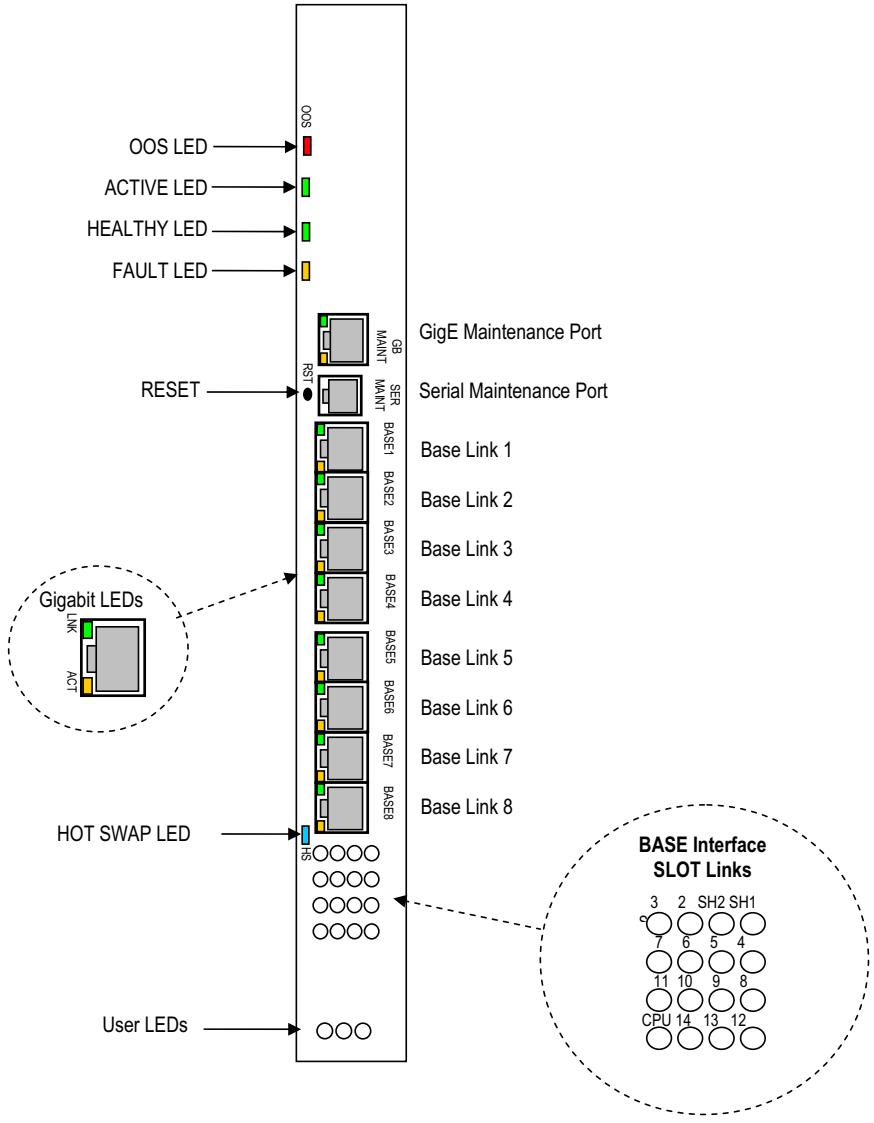
# 1.8.1 aTCA-3100
![Based on the provided image, here is the accurate and concise description of the flowchart/block diagram:\n\n**Top Status Indicators**\n*   **OOS LED**: Points to a red block labeled **OOS**.\n*   **ACTIVE LED**: Points to a green block.\n*   **HEALTHY LED**: Points to a green block.\n*   **FAULT LED**: Points to a yellow block.\n\n**Main Interface Strip (Left to Right Connections)**\n*   **GigE Maintenance Port**: Labeled next to a port marked **GB** and **MAINT**.\n*   **Serial Maintenance Port**: Labeled next to a switch marked **SFR** and **MAINT**.\n*   **RESET**: Points to a switch/dot labeled **RS17**.\n*   **Base Link 1** through **Base Link 8**: Correspond to ports labeled **BASE1** through **BASE8** respectively.\n\n**Lower Indicators**\n*   **HOT SWAP LED**: Points to a blue switch labeled **HS**.\n*   **User LEDs**: Points to a row of three circles at the bottom.\n\n**Detailed Callouts (Dashed Circles)**\n*   **Gigabit LEDs**: A dashed circle pointing to the BASE ports, showing details for **LINK** (green) and **ACT** (yellow) lights.\n*   **BASE Interface SLOT Links**: A dashed circle pointing to a grid of circles below the HS switch, labeled with the following identifiers: **3**, **2**, **SH2**, **SH1**, **7**, **6**, **5**, **4**, **11**, **10**, **9**, **8**, **CPU**, **14**, **13**, **12**.](.atca-3100series-manual-3/f3ec95fbc1cc29b063b0d8fcf68df18168af817bfd2ced8ce7b47b562c2b3741.jpg)

Figure 1-7: aTCA-3100 front panel

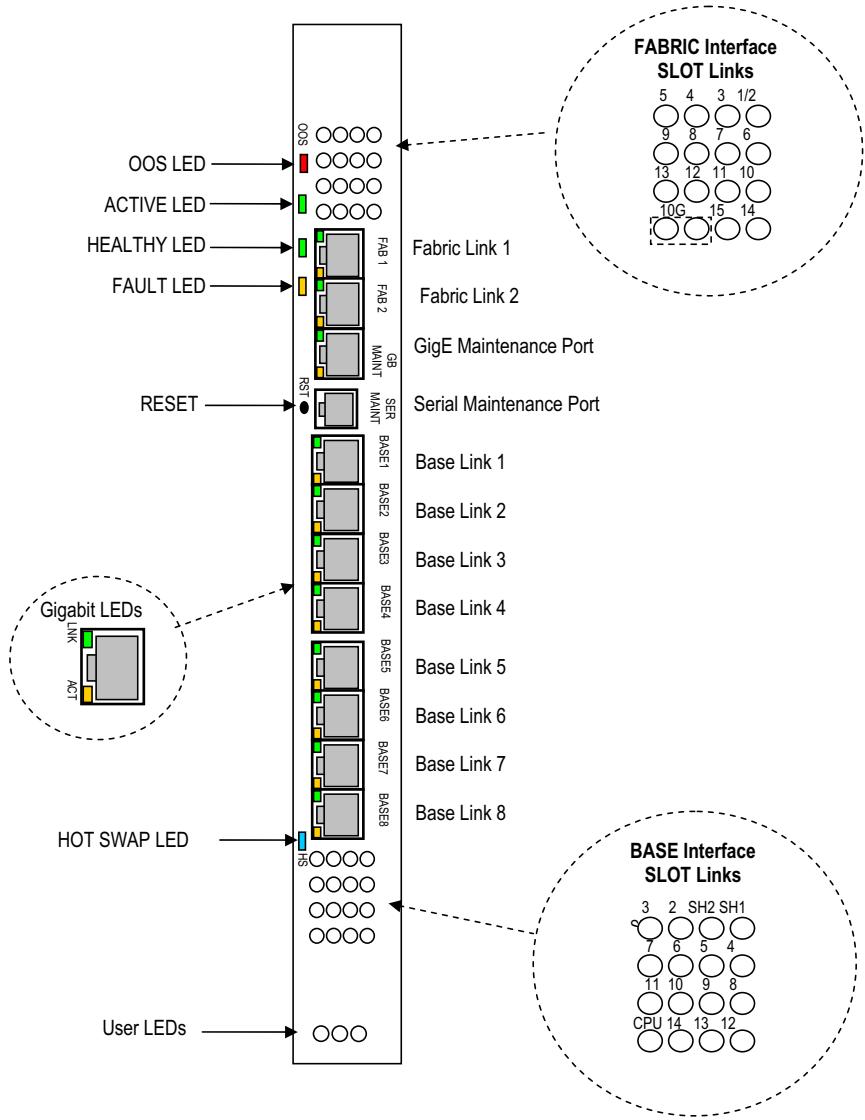
1.8.2 aTCA-3110
![OOS LED\nACTIVE LED\nHEALTHY LED\nFAULT LED\nRESET\nGigabit LEDs\nHOT SWAP LED\nUser LEDs\nFAB1\nFAB2\nGB\nMAINT\nSER\nBASE1\nBASE2\nBASE3\nBASE4\nBASE5\nBASE6\nBASE7\nBASE8\nFabric Link 1\nFabric Link 2\nGigE Maintenance Port\nSerial Maintenance Port\nBase Link 1\nBase Link 2\nBase Link 3\nBase Link 4\nBase Link 5\nBase Link 6\nBase Link 7\nBase Link 8\nBASE Interface SLOT Links\n5 4 3 1/2\n9 8 7 6\n13 12 11 10\n10G 15 14\nBASE Interface SLOT Links\n3 2 SH2 SH1\n7 6 5 4\n11 10 9 8\nCPU 14 13 12](.atca-3100series-manual-3/c15f745036c3fb06c519fb20121cad5b626d56e9aef2b33b482b876357b09fa7.jpg)

Figure 1-8: aTCA-3110 front panel

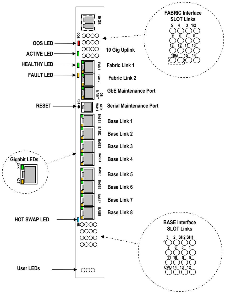
1.8.3 aTCA-3120
![Based on the provided image, here is an accurate and concise description of the flowchart/block diagram, listing labeled blocks and connections verbatim:\n\n**Top Section (10 Gig Uplink)**\n*   **Block:** A port block labeled '10 GB'.\n*   **Indicators:** Four LED indicators on the left labeled 'OOS LED', 'ACTIVE LED', 'HEALTHY LED', and 'FAULT LED'. (Note: The vertical text 'OOS' appears next to the LED row).\n*   **Description:** The text '10 Gig Uplink' is positioned to the right.\n*   **Connection:** A dashed arrow points from this section to a callout circle labeled 'FABRIC Interface SLOT Links'.\n    *   **Callout Contents:** Numbered circles arranged in rows: '5 4 3 1/2', '9 8 7 6', '13 12 11 10', and '10G 15 14'.\n\n**Middle Section (Fabric and Maintenance)**\n*   **Ports:** Two port blocks labeled vertically 'FAB 1' and 'FAB 2'.\n*   **Descriptions:** Corresponding labels to the right: 'Fabric Link 1' and 'Fabric Link 2'.\n*   **Ports:** Two port blocks labeled vertically 'MAINT' and 'RS1'. (Vertical text 'GB' is next to MAINT, and 'SER' is next to RS1).\n*   **Descriptions:** Corresponding labels to the right: 'GbE Maintenance Port' and 'Serial Maintenance Port'.\n*   **Button:** A label 'RESET' points to a small circular button.\n\n**Lower Middle Section (Base Links)**\n*   **Ports:** Eight port blocks labeled vertically 'BASE1' through 'BASE8'.\n*   **Descriptions:** Corresponding labels to the right: 'Base Link 1' through 'Base Link 8'.\n*   **Connection:** A dashed arrow points from a callout circle labeled 'Gigabit LEDs' to these ports.\n    *   **Callout Contents:** A single port diagram with LEDs labeled 'LINK' and 'ACT'.\n\n**Bottom Section (Hot Swap and User LEDs)**\n*   **Block:** A block labeled 'HS'.\n*   **Indicators:**\n    *   A label 'HOT SWAP LED' points to a blue LED.\n    *   A label 'User LEDs' points to three empty circles.\n*   **Connection:** A dashed arrow points from the bottom section (near the User LEDs) to a callout circle labeled 'BASE Interface SLOT Links'.\n    *   **Callout Contents:** Numbered circles arranged in rows: '3 2 SH2 SH1', '7 6 5 4', '11 10 9 8', and 'CPU 14 13 12'.](.atca-3100series-manual-3/32e66c19122d8c30ebbd18e73a981043ecf62f4744879d07d2b5f9b5cfce4988.jpg)

Figure 1-9: aTCA-3120 front panel

# 1.9 Configuration switches

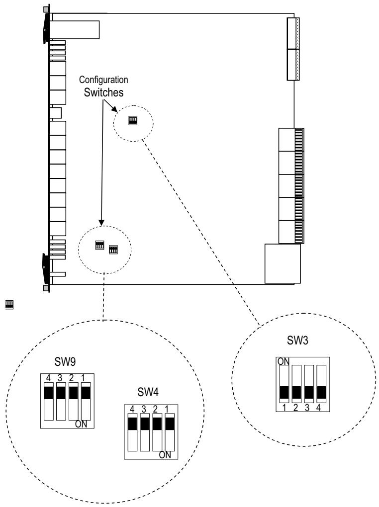
The aTCA-3100 Series have two four position switch blocks that can be used for card configuration.
![The diagram depicts a system layout with detailed callouts for switches.\n\n**Labeled Blocks and Text:**\n*   **Configuration Switches:** Text pointing to a switch icon.\n*   **SW9:** A block containing switch labels '4 3 2 1' and 'ON'.\n*   **SW4:** A block containing switch labels '4 3 2 1' and 'ON'.\n*   **SW3:** A block containing switch label 'ON' and labels '1 2 3 4'.\n\n**Connections:**\n*   A solid arrow points from the text 'Configuration Switches' to a switch icon within a dashed circle.\n*   A solid arrow points from that icon down to another dashed circle containing two switch icons.\n*   A dashed line connects the lower dashed circle (containing two switches) to a large dashed circle at the bottom left containing the **SW9** and **SW4** blocks.\n*   A dashed line connects a switch icon on the right side of the main diagram to a large dashed circle at the bottom right containing the **SW3** block.](.atca-3100series-manual-3/119945b0295e730c00fe607961e57fcabdcf0fe1cbfd9f51a286af6fc9af18e5.jpg)

Figure 1-10: aTCA-3100 Series switch locations

# 1.9.1 Switch 3

SW3 is used as an option selection switch. The base and fabric configuration parameters are saved automatically based on the setting of these four switches.

<table><tr><td>Switch</td><td>Description</td></tr><tr><td>1</td><td>Payload Option Select Switch (ON = 0, OFF= 1)</td></tr><tr><td>2</td><td>Payload Option Select Switch (ON = 0, OFF= 1)</td></tr><tr><td>3</td><td>Payload Option Select Switch (ON = 0, OFF= 1)</td></tr><tr><td>4</td><td>Payload Option Select Switch (ON = 0, OFF= 1)</td></tr></table>

Table 1-3: Switch 3 description

Options selection

<table><tr><td rowspan="2">Options</td><td colspan="4">Switch selections</td></tr><tr><td>4</td><td>3</td><td>2</td><td>1</td></tr><tr><td>Option 1 (Default)</td><td>0</td><td>0</td><td>0</td><td>0</td></tr><tr><td>Option 2</td><td>0</td><td>0</td><td>0</td><td>1</td></tr><tr><td>Option 3</td><td>0</td><td>0</td><td>1</td><td>0</td></tr><tr><td>Option 4</td><td>0</td><td>0</td><td>1</td><td>1</td></tr><tr><td>Option 5</td><td>0</td><td>1</td><td>0</td><td>0</td></tr><tr><td>Option 6</td><td>0</td><td>1</td><td>0</td><td>1</td></tr><tr><td>Option 7</td><td>0</td><td>1</td><td>1</td><td>0</td></tr><tr><td>Option 8</td><td>0</td><td>1</td><td>1</td><td>1</td></tr><tr><td>Option 9</td><td>1</td><td>0</td><td>0</td><td>0</td></tr><tr><td>Option 10</td><td>1</td><td>0</td><td>0</td><td>1</td></tr><tr><td>Option 11</td><td>1</td><td>0</td><td>1</td><td>0</td></tr><tr><td>Option 12</td><td>1</td><td>0</td><td>1</td><td>1</td></tr><tr><td>Option 13</td><td>1</td><td>1</td><td>0</td><td>0</td></tr><tr><td>Option 14</td><td>1</td><td>1</td><td>0</td><td>1</td></tr><tr><td>Option 15</td><td>1</td><td>1</td><td>1</td><td>0</td></tr><tr><td>Option 16</td><td>1</td><td>1</td><td>1</td><td>1</td></tr></table>

Table 1-4: Options selection for SW3

NOTE Refer to the aTCA-31xx Configuration Guide for additional information on option configuration files.

# 1.9.2 Switch 4

<table><tr><td>Switch</td><td>Description</td></tr><tr><td>1</td><td>IPMC Flash Write Enable(ON = Disable, OFF = Enable, Default = ON)</td></tr><tr><td>2</td><td>IPMC Payload PROM Boot Select Switch (Default = OFF)</td></tr><tr><td>3</td><td>ShMC Ethernet Select(OFF = Dual 100 Mb, ON = Single GbE, Default = OFF)</td></tr><tr><td>4</td><td>IPMC Stand-Alone Switch (ON = Stand-Alone, OFF = Normal)</td></tr></table>

Table 1-5: Switch 4 description

# 1.9.3 Switch 9

<table><tr><td>Switch</td><td>Description</td></tr><tr><td>1</td><td>IPMC NMI Configuration Selection(ON=0, OFF=1, Default = OFF)</td></tr><tr><td>2</td><td>IPMC MD2 Configuration Selection(ON=0, OFF=1, Default = OFF)</td></tr><tr><td>3</td><td>IPMC MD1 Configuration Selection(ON=0, OFF=1, Default = OFF)</td></tr><tr><td>4</td><td>IPMC MD0 Configuration Selection(ON=0, OFF=1, Default = OFF)</td></tr></table>

Table 1-6: Switch 9 description

NOTE This switch is for IPMC debug purposes. The switches must be left in their default configurations (normal operating mode).

# 2 Installation

# 2.1 Installing the card

The aTCA-3100 Series switch blade installs into a standard AdvancedTCA chassis. The card is intended to be installed into switch slots that are logic slot 1 and 2 in the chassis.

When installing the card into a chassis, make sure that the card is seated correctly and the card ejector latches are fully engaged. If the left ejector latch is not engaged, the card will not power-up and boot.

![Shelf Management Cards\nATCA chassis\nATCA-3120 hub cards](.atca-3100series-manual-3/fcffc4920cb1a3e0d34629ae91b608ad5341413df5c4d0ddda82025f2eec463c.jpg)

# 2.1.1 Connecting the serial cable

To initially use the card and develop applications you will need a serial cable. The serial cable required for use with standard COM ports is shown below. It is an RJ11 to female DB9 converter. This cable connects the card's serial port (RJ-11), to a standard PC COM port..

![COM Port Cable\n1\n2\n3\n4\nRJ-11\n9-pin D-Sub, Female\n1\n2\n3\n4\n5\n6\n7\n8\n9](.atca-3100series-manual-3/204641ac9f68121ce7be740805ce7092b4f41a2da9618cb0d5f10e8637bea88e.jpg)

This table below shows the connections when using either a 6-pin or 4-pin RJ-11 connector.

<table><tr><td>6-pin RJ-11</td><td>4-pin RJ-11</td><td>9-pin D-Sub pin#</td><td>9-pin D-Sub pin#</td></tr><tr><td>1</td><td></td><td>(Not Used)</td><td>Chassis Ground</td></tr><tr><td>2</td><td>1</td><td>3</td><td>TX</td></tr><tr><td>3</td><td>2</td><td>2</td><td>RX</td></tr><tr><td>4</td><td>3</td><td>5</td><td>Ground</td></tr><tr><td>5</td><td>4</td><td>(Not Used)</td><td>Ground</td></tr><tr><td>6</td><td></td><td>(Not Used)</td><td>Ground</td></tr></table>

Connect the serial cable to the computer's serial port (COM1 or COM2) and to the aTCA-3100 Series card serial interface. Refer to the illustration below..

![PC or laptop computer\nSerial cable\nATCA-3120\nRST\nMAINT\nSER\nMAINT\nBASE1\nBASE2\nBASE3](.atca-3100series-manual-3/ffab93b2900571716698c6a7a3e7eeb55fbba27bfa926ceadec2839f17144f1a.jpg)

# 2.1.2 Accessing the aTCA-3100 Series card

Follow these steps to connect the aTCA-3100 Series card to the development platform host system:

1. Use the serial cable to connect the aTCA-3100 Series card to the serial port on the development host.
2. Run a terminal emulation program from the development host (e.g. HyperTerminal for Microsoft® Windows® systems or minicom for Linux systems), then configure the program for VT100 emulation with the following set of

communication settings: no flow control, no parity bits, 8 data bits, 1 stop bit, and 115200 baud rate.

3. Reset or power-up the aTCA-3100 Series card. It takes about one and a half minutes to boot to the Linux prompt after the shelf manager commands the board to power up.

# 2.1.3 Firmware boot sequence

The following boot sequence is executed when the board is powered.

▶ Boot Monitor (RedBoot)

The Boot Monitor is based on RedBoot, which is an acronym for RedHat Embedded Debug and Bootstrap. RedBoot is used to load and boot Linux.

▶ Linux Kernel, Filesystem

The RedBoot Loader automatically boots Linux. Refer to the aTCA-3100 Series Configuration Guide for more information on Linux configurations.

▶ Switch Software

The switch software and drivers are automatically loaded under Linux. The switch software consists of background drivers and configuration utilities for both base and fabric interfaces. The base interface is configured using cli-base and the fabric interface can be configured using cli-fabric. Refer to the aTCA-3100 Series Configuration Guide for additional information.

# 3 Connector Pinouts

3.1 Zone 1 connector (P10)

<table><tr><td>Pin #</td><td>Signal</td><td>Description</td></tr><tr><td>1</td><td>(Reserved)</td><td>Reserved (Not Connected)</td></tr><tr><td>2</td><td>(Reserved)</td><td>Reserved, (Not Connected)</td></tr><tr><td>3</td><td>(Reserved)</td><td>Reserved, (Not Connected)</td></tr><tr><td>4</td><td>(Reserved)</td><td>Reserved, (Not Connected)</td></tr><tr><td>5</td><td>HA0</td><td>HA0 Hardware Address Bit 0</td></tr><tr><td>6</td><td>HA1</td><td>HA1 Hardware Address Bit 1</td></tr><tr><td>7</td><td>HA2</td><td>HA2 Hardware Address Bit 2</td></tr><tr><td>8</td><td>HA3</td><td>HA3 Hardware Address Bit 3</td></tr><tr><td>9</td><td>HA4</td><td>HA4 Hardware Address Bit 4</td></tr><tr><td>10</td><td>HA5</td><td>HA5 Hardware Address Bit 5</td></tr><tr><td>11</td><td>HA6</td><td>HA6 Hardware Address Bit 6d</td></tr><tr><td>12</td><td>HA7/P</td><td>HA7/P Hardware Address Bit 7 (Odd Parity Bit)</td></tr><tr><td>13</td><td>SCL_A</td><td>IPMB Clock, Port A</td></tr><tr><td>14</td><td>SDA_A</td><td>IPMB Data, Port A</td></tr><tr><td>15</td><td>SCL_B</td><td>IPMB Clock, Port B</td></tr><tr><td>16</td><td>SDA_B</td><td>IPMB Data, Port B</td></tr><tr><td>17</td><td>MT1_TIP</td><td>Unused (Not Connected)</td></tr><tr><td>18</td><td>MT2_TIP</td><td>Unused (Not Connected)</td></tr><tr><td>19</td><td>-RING_A</td><td>Unused (Not Connected)</td></tr><tr><td>20</td><td>-RING_B</td><td>Unused (Not Connected)</td></tr><tr><td>21</td><td>MT1_RING</td><td>Unused (Not Connected)</td></tr><tr><td>22</td><td>MT2_RING</td><td>Unused (Not Connected)</td></tr><tr><td>23</td><td>RRTN_A</td><td>Unused (Not Connected)</td></tr><tr><td>24</td><td>RRTN_B</td><td>Unused (Not Connected)</td></tr><tr><td>25</td><td>SHELF_GND</td><td>Connection to Shelf Ground and safety ground</td></tr><tr><td>26</td><td>LOGIC_GND</td><td>Ground reference and return for logic signals</td></tr><tr><td>27</td><td>ENABLE_B</td><td>Short pin for -48V Feed B power sequencing</td></tr><tr><td>28</td><td>VRTN_A</td><td>Voltage Return A -48 Volt return</td></tr><tr><td>29</td><td>VRTN_B</td><td>Voltage Return B -48 Volt return</td></tr><tr><td>30</td><td>EARLY_A</td><td>-48 Volt Early A -48 Volt input, Unused (Not Connected)</td></tr><tr><td>31</td><td>EARLY_B</td><td>-48 Volt Early B -48 Volt input, Unused (Not Connected)</td></tr></table>

Table 3-1: Zone 1 connector P10

<table><tr><td>Pin #</td><td>Signal</td><td>Description</td></tr><tr><td>32</td><td>ENABLE_A</td><td>Short pin for -48V Feed A power sequencing</td></tr><tr><td>33</td><td>-48V_A</td><td>-48 Volt input, Min power Feed A</td></tr><tr><td>34</td><td>-48V_B</td><td>-48 Volt input, Main Power Feed B</td></tr></table>

Table 3-1: Zone 1 connector P10

# 3.2 Zone 2 connectors

# 3.2.1 J20

<table><tr><td>ROWS</td><td>A</td><td>B</td><td>GND AB</td><td>C</td><td>D</td><td>GND CD</td><td>E</td><td>F</td><td>GNDEF</td><td>G</td><td>H</td><td>GND GH</td></tr><tr><td>1</td><td>N/C</td><td>N/C</td><td>N/C</td><td>N/C</td><td>N/C</td><td>GND</td><td>N/C</td><td>N/C</td><td>GND</td><td>N/C</td><td>N/C</td><td>GND</td></tr><tr><td>2</td><td>N/C</td><td>N/C</td><td>GND</td><td>N/C</td><td>N/C</td><td>GND</td><td>N/C</td><td>N/C</td><td>GND</td><td>N/C</td><td>N/C</td><td>GND</td></tr><tr><td>3</td><td>N/C</td><td>N/C</td><td>GND</td><td>N/C</td><td>N/C</td><td>GND</td><td>N/C</td><td>N/C</td><td>GND</td><td>N/C</td><td>N/C</td><td>GND</td></tr><tr><td>4</td><td>N/C</td><td>N/C</td><td>GND</td><td>N/C</td><td>N/C</td><td>GND</td><td>N/C</td><td>N/C</td><td>GND</td><td>N/C</td><td>N/C</td><td>GND</td></tr><tr><td>5</td><td>N/C</td><td>N/C</td><td>GND</td><td>TERM</td><td>TERM</td><td>GND</td><td>N/C</td><td>N/C</td><td>GND</td><td>TERM</td><td>TERM</td><td>GND</td></tr><tr><td>6</td><td>N/C</td><td>N/C</td><td>GND</td><td>TERM</td><td>TERM</td><td>GND</td><td>N/C</td><td>N/C</td><td>GND</td><td>TERM</td><td>TERM</td><td>GND</td></tr><tr><td>7</td><td>N/C</td><td>N/C</td><td>GND</td><td>TERM</td><td>TERM</td><td>GND</td><td>N/C</td><td>N/C</td><td>GND</td><td>TERM</td><td>TERM</td><td>GND</td></tr><tr><td>8</td><td>N/C</td><td>N/C</td><td>GND</td><td>TERM</td><td>TERM</td><td>GND</td><td>N/C</td><td>N/C</td><td>GND</td><td>TERM</td><td>TERM</td><td>GND</td></tr><tr><td>9</td><td>N/C</td><td>N/C</td><td>GND</td><td>TERM</td><td>TERM</td><td>GND</td><td>N/C</td><td>N/C</td><td>GND</td><td>TERM</td><td>TERM</td><td>GND</td></tr><tr><td>10</td><td>FCH1 2_TXp</td><td>FCH1 2_TXn</td><td>GND</td><td>FCH1 2_RXp</td><td>FCH1 2_RXn</td><td>GND</td><td>N/C</td><td>N/C</td><td>GND</td><td>TERM</td><td>TERM</td><td>GND</td></tr></table>

Table 3-2: J20 connector

# 3.2.2 J21

<table><tr><td>ROWS</td><td>A</td><td>B</td><td>GND AB</td><td>C</td><td>D</td><td>GND CD</td><td>E</td><td>F</td><td>GND EF</td><td>G</td><td>H</td><td>GND GH</td></tr><tr><td>1</td><td>N/C</td><td>N/C</td><td>GND</td><td>TERM</td><td>TERM</td><td>GND</td><td>N/C</td><td>N/C</td><td>GND</td><td>TERM</td><td>TERM</td><td>GND</td></tr><tr><td>2</td><td>FCH11_TXp</td><td>FCH11_TXn</td><td>GND</td><td>FCH11_RXp</td><td>FCH11_RXn</td><td>GND</td><td>N/C</td><td>N/C</td><td>GND</td><td>TERM</td><td>TERM</td><td>GND</td></tr><tr><td>3</td><td>N/C</td><td>N/C</td><td>GND</td><td>TERM</td><td>TERM</td><td>GND</td><td>N/C</td><td>N/C</td><td>GND</td><td>TERM</td><td>TERM</td><td>GND</td></tr><tr><td>4</td><td>FCH10_TXp</td><td>FCH10_TXn</td><td>GND</td><td>FCH10_RXp</td><td>FCH10_RXn</td><td>GND</td><td>N/C</td><td>N/C</td><td>GND</td><td>TERM</td><td>TERM</td><td>GND</td></tr><tr><td>5</td><td>N/C</td><td>N/C</td><td>GND</td><td>TERM</td><td>TERM</td><td>GND</td><td>N/C</td><td>N/C</td><td>GND</td><td>TERM</td><td>TERM</td><td>GND</td></tr><tr><td>6</td><td>FCH9_TXp</td><td>FCH9_TXn</td><td>GND</td><td>FCH9_RXp</td><td>FCH9_RXn</td><td>GND</td><td>N/C</td><td>N/C</td><td>GND</td><td>TERM</td><td>TERM</td><td>GND</td></tr><tr><td>7</td><td>N/C</td><td>N/C</td><td>GND</td><td>TERM</td><td>TERM</td><td>GND</td><td>N/C</td><td>N/C</td><td>GND</td><td>TERM</td><td>TERM</td><td>GND</td></tr><tr><td>8</td><td>FCH8_TXp</td><td>FCH8_TXn</td><td>GND</td><td>FCH8_RXp</td><td>FCH8_RXn</td><td>GND</td><td>N/C</td><td>N/C</td><td>GND</td><td>TERM</td><td>TERM</td><td>GND</td></tr><tr><td>9</td><td>N/C</td><td>N/C</td><td>GND</td><td>TERM</td><td>TERM</td><td>GND</td><td>N/C</td><td>N/C</td><td>GND</td><td>TERM</td><td>TERM</td><td>GND</td></tr><tr><td>10</td><td>FCH7_TXp</td><td>FCH7_TXn</td><td>GND</td><td>FCH7_RXp</td><td>FCH7_RXn</td><td>GND</td><td>N/C</td><td>N/C</td><td>GND</td><td>TERM</td><td>TERM</td><td>GND</td></tr></table>

Table 3-3: J21 connector

# 3.2.3 J22

<table><tr><td>ROWS</td><td>A</td><td>B</td><td>GND AB</td><td>C</td><td>D</td><td>GND CD</td><td>E</td><td>F</td><td>GND EF</td><td>G</td><td>H</td><td>GND GH</td></tr><tr><td>1</td><td>N/C</td><td>N/C</td><td>GND</td><td>TERM</td><td>TERM</td><td>GND</td><td>N/C</td><td>N/C</td><td>GND</td><td>TERM</td><td>TERM</td><td>GND</td></tr><tr><td>2</td><td>FCH11_TXp</td><td>FCH11_TXn</td><td>GND</td><td>FCH11_RXp</td><td>FCH11_RXn</td><td>GND</td><td>N/C</td><td>N/C</td><td>GND</td><td>TERM</td><td>TERM</td><td>GND</td></tr><tr><td>3</td><td>N/C</td><td>N/C</td><td>GND</td><td>TERM</td><td>TERM</td><td>GND</td><td>N/C</td><td>N/C</td><td>GND</td><td>TERM</td><td>TERM</td><td>GND</td></tr><tr><td>4</td><td>FCH10_TXp</td><td>FCH10_TXn</td><td>GND</td><td>FCH10_RXp</td><td>FCH10_RXn</td><td>GND</td><td>N/C</td><td>N/C</td><td>GND</td><td>TERM</td><td>TERM</td><td>GND</td></tr><tr><td>5</td><td>N/C</td><td>N/C</td><td>GND</td><td>TERM</td><td>TERM</td><td>GND</td><td>N/C</td><td>N/C</td><td>GND</td><td>TERM</td><td>TERM</td><td>GND</td></tr><tr><td>6</td><td>FCH9_TXp</td><td>FCH9_TXn</td><td>GND</td><td>FCH9_RXp</td><td>FCH9_RXn</td><td>GND</td><td>N/C</td><td>N/C</td><td>GND</td><td>TERM</td><td>TERM</td><td>GND</td></tr><tr><td>7</td><td>N/C</td><td>N/C</td><td>GND</td><td>TERM</td><td>TERM</td><td>GND</td><td>N/C</td><td>N/C</td><td>GND</td><td>TERM</td><td>TERM</td><td>GND</td></tr><tr><td>8</td><td>FCH8_TXp</td><td>FCH8_TXn</td><td>GND</td><td>FCH8_RXp</td><td>FCH8_RXn</td><td>GND</td><td>N/C</td><td>N/C</td><td>GND</td><td>TERM</td><td>TERM</td><td>GND</td></tr><tr><td>9</td><td>N/C</td><td>N/C</td><td>GND</td><td>TERM</td><td>TERM</td><td>GND</td><td>N/C</td><td>N/C</td><td>GND</td><td>TERM</td><td>TERM</td><td>GND</td></tr><tr><td>10</td><td>FCH7_TXp</td><td>FCH7_TXn</td><td>GND</td><td>FCH7_RXp</td><td>FCH7_RXn</td><td>GND</td><td>N/C</td><td>N/C</td><td>GND</td><td>TERM</td><td>TERM</td><td>GND</td></tr></table>

Table 3-4: J22 connector

# 3.2.4 J23

<table><tr><td>ROWS</td><td>A</td><td>B</td><td>GND AB</td><td>C</td><td>D</td><td>GND CD</td><td>E</td><td>F</td><td>GNDEF</td><td>G</td><td>H</td><td>GND GH</td></tr><tr><td>1</td><td>N/C</td><td>N/C</td><td>GND</td><td>TERM</td><td>TERM</td><td>GND</td><td>N/C</td><td>N/C</td><td>GND</td><td>TERM</td><td>TERM</td><td>GND</td></tr><tr><td>2</td><td>FCH1_TX p</td><td>FCH1_TX n</td><td>GND</td><td>FCH1_RXp</td><td>FCH1_RXn</td><td>GND</td><td>N/C</td><td>N/C</td><td>GND</td><td>TERM</td><td>TERM</td><td>GND</td></tr><tr><td>3</td><td>N/C</td><td>N/C</td><td>GND</td><td>TERM</td><td>TERM</td><td>GND</td><td>N/C</td><td>N/C</td><td>GND</td><td>TERM</td><td>TERM</td><td>GND</td></tr><tr><td>4</td><td>FCH0_TX p</td><td>FCH0_TX n</td><td>GND</td><td>FCH0_RXp</td><td>FCH0_RXn</td><td>GND</td><td>N/C</td><td>N/C</td><td>GND</td><td>TERM</td><td>TERM</td><td>GND</td></tr><tr><td>5</td><td>BCH1_Ap</td><td>BCH1_An</td><td>GND</td><td>BCH1_Bp</td><td>BCH1_Bn</td><td>GND</td><td>BCH1_Cp</td><td>BCH1_Cn</td><td>GND</td><td>BCH1_Dp</td><td>BCH1_Dn</td><td>GND</td></tr><tr><td>6</td><td>BCH2_Ap</td><td>BCH2_An</td><td>GND</td><td>BCH2_Bp</td><td>BCH2_Bn</td><td>GND</td><td>BCH2_Cp</td><td>BCH2_Cn</td><td>GND</td><td>BCH2_Dp</td><td>BCH2_Dn</td><td>GND</td></tr><tr><td>7</td><td>BCH3_Ap</td><td>BCH3_An</td><td>GND</td><td>BCH3_Bp</td><td>BCH3_Bn</td><td>GND</td><td>BCH3_Cp</td><td>BCH3_Cn</td><td>GND</td><td>BCH3_Dp</td><td>BCH3_Dn</td><td>GND</td></tr><tr><td>8</td><td>BCH4_Ap</td><td>BCH4_An</td><td>GND</td><td>BCH4_Bp</td><td>BCH4_Bn</td><td>GND</td><td>BCH4_Cp</td><td>BCH4_Cn</td><td>GND</td><td>BCH4_Dp</td><td>BCH4_Dn</td><td>GND</td></tr><tr><td>9</td><td>BCH5_Ap</td><td>BCH5_An</td><td>GND</td><td>BCH5_Bp</td><td>BCH5_Bn</td><td>GND</td><td>BCH5_Cp</td><td>BCH5_Cn</td><td>GND</td><td>BCH5_Dp</td><td>BCH5_Dn</td><td>GND</td></tr><tr><td>10</td><td>BCH6_Ap</td><td>BCH6_An</td><td>GND</td><td>BCH6_Bp</td><td>BCH6_Bn</td><td>GND</td><td>BCH6_Cp</td><td>BCH6_Cn</td><td>GND</td><td>BCH6_Dp</td><td>BCH6_Dn</td><td>GND</td></tr></table>

Table 3-5: J23 connector

# 3.2.5 J24

<table><tr><td>ROWS</td><td>A</td><td>B</td><td>GND AB</td><td>C</td><td>D</td><td>GND CD</td><td>E</td><td>F</td><td>GND EF</td><td>G</td><td>H</td><td>GND GH</td></tr><tr><td>1</td><td>BCH7_Ap</td><td>BCH7_An</td><td>GND</td><td>BCH7_Bp</td><td>BCH7_Bn</td><td>GND</td><td>BCH7_Cp</td><td>BCH7_Cn</td><td>GND</td><td>BCH7_Dp</td><td>BCH7_Dn</td><td>GND</td></tr><tr><td>2</td><td>BCH8_Ap</td><td>BCH8_An</td><td>GND</td><td>BCH8_Bp</td><td>BCH8_Bn</td><td>GND</td><td>BCH8_Cp</td><td>BCH8_Cn</td><td>GND</td><td>BCH8_Dp</td><td>BCH8_Dn</td><td>GND</td></tr><tr><td>3</td><td>BCH9_Ap</td><td>BCH9_An</td><td>GND</td><td>BCH9_Bp</td><td>BCH9_Bn</td><td>GND</td><td>BCH9_Cp</td><td>BCH9_Cn</td><td>GND</td><td>BCH9_Dp</td><td>BCH9_Dn</td><td>GND</td></tr><tr><td>4</td><td>BCH10_Ap</td><td>BCH10_An</td><td>GND</td><td>BCH10_Bp</td><td>BCH10_Bn</td><td>GND</td><td>BCH10_Cp</td><td>BCH10_Cn</td><td>GND</td><td>BCH10_Dp</td><td>BCH10_Dn</td><td>GND</td></tr><tr><td>5</td><td>BCH11_Ap</td><td>BCH11_An</td><td>GND</td><td>BCH11_Bp</td><td>BCH11_Bn</td><td>GND</td><td>BCH11_Cp</td><td>BCH11_Cn</td><td>GND</td><td>BCH11_Dp</td><td>BCH11_Dn</td><td>GND</td></tr><tr><td>6</td><td>BCH12_Ap</td><td>BCH12_An</td><td>GND</td><td>BCH12_Bp</td><td>BCH12_Bn</td><td>GND</td><td>BCH12_Cp</td><td>BCH12_Cn</td><td>GND</td><td>BCH12_Dp</td><td>BCH12_Dn</td><td>GND</td></tr><tr><td>7</td><td>BCH13_Ap</td><td>BCH13_An</td><td>GND</td><td>BCH13_Bp</td><td>BCH13_Bn</td><td>GND</td><td>BCH13_Cp</td><td>BCH13_Cn</td><td>GND</td><td>BCH13_Dp</td><td>BCH13_Dn</td><td>GND</td></tr><tr><td>8</td><td>BCH14_Ap</td><td>BCH14_An</td><td>GND</td><td>BCH14_Bp</td><td>BCH14_Bn</td><td>GND</td><td>BCH14_Cp</td><td>BCH14_Cn</td><td>GND</td><td>BCH14_Dp</td><td>BCH14_Dn</td><td>GND</td></tr><tr><td>9</td><td>N/C</td><td>N/C</td><td>GND</td><td>N/C</td><td>N/C</td><td>GND</td><td>N/C</td><td>N/C</td><td>GND</td><td>N/C</td><td>N/C</td><td>GND</td></tr><tr><td>10</td><td>N/C</td><td>N/C</td><td>GND</td><td>N/C</td><td>N/C</td><td>GND</td><td>N/C</td><td>N/C</td><td>GND</td><td>N/C</td><td>N/C</td><td>GND</td></tr></table>

Table 3-6: J24 connector

# 3.3 Zone 3 connectors

# 3.3.1 J2 Rear I/O connector

<table><tr><td>ROW #</td><td>A</td><td>B</td><td>C</td><td>D</td><td>E</td><td>F</td></tr><tr><td>19</td><td>N/C</td><td>N/C</td><td>N/C</td><td>N/C</td><td>N/C</td><td>GND</td></tr><tr><td>18</td><td>N/C</td><td>N/C</td><td>N/C</td><td>N/C</td><td>N/C</td><td>GND</td></tr><tr><td>17</td><td>N/C</td><td>N/C</td><td>N/C</td><td>N/C</td><td>N/C</td><td>GND</td></tr><tr><td>16</td><td>N/C</td><td>N/C</td><td>N/C</td><td>N/C</td><td>N/C</td><td>GND</td></tr><tr><td>15</td><td>N/C</td><td>N/C</td><td>N/C</td><td>N/C</td><td>N/C</td><td>GND</td></tr><tr><td>14</td><td>N/C</td><td>N/C</td><td>N/C</td><td>N/C</td><td>N/C</td><td>GND</td></tr><tr><td>13</td><td>GND</td><td>GND</td><td>GND</td><td>GND</td><td>GND</td><td>GND</td></tr><tr><td>12</td><td>GND</td><td>CH23_RD2</td><td>CH23_RD3</td><td>CH23_TD2</td><td>CH23_TD3</td><td>GND</td></tr><tr><td>11</td><td>GND</td><td>CH23_RD0</td><td>CH23_RD1</td><td>CH23_TD0</td><td>CH23_TD1</td><td>GND</td></tr><tr><td>10</td><td>GND</td><td>CH23_RXCLK</td><td>CH23_RXCTL</td><td>CH23_TXCLK</td><td>CH23_TXCTL</td><td>GND</td></tr><tr><td>9</td><td>GND</td><td>GND</td><td>GND</td><td>GND</td><td>GND</td><td>GND</td></tr><tr><td>8</td><td>GND</td><td>CH22_RD2</td><td>CH22_RD3</td><td>CH22_TD2</td><td>CH22_TD3</td><td>GND</td></tr><tr><td>7</td><td>GND</td><td>CH22_RD0</td><td>CH22_RD1</td><td>CH22_TD0</td><td>CH22_TD1</td><td>GND</td></tr><tr><td>6</td><td>GND</td><td>CH22_RXCLK</td><td>CH22_RXCTL</td><td>CH22_TXCLK</td><td>CH22_TXCTL</td><td>GND</td></tr><tr><td>5</td><td>GND</td><td>GND</td><td>GND</td><td>GND</td><td>GND</td><td>GND</td></tr><tr><td>4</td><td>GND</td><td>CH21_RD2</td><td>CH21_RD3</td><td>CH21_TD2</td><td>CH21_TD3</td><td>GND</td></tr><tr><td>3</td><td>GND</td><td>CH21_RD0</td><td>CH21_RD1</td><td>CH21_TD0</td><td>CH21_TD1</td><td>GND</td></tr><tr><td>2</td><td>GND</td><td>CH21_RXCLK</td><td>CH21_RXCTL</td><td>CH21_TXCLK</td><td>CH21_TXCTL</td><td>GND</td></tr><tr><td>1</td><td>GND</td><td>GND</td><td>GND</td><td>GND</td><td>GND</td><td>GND</td></tr></table>

Table 3-7: J2 RTM connector

# 3.3.2 J1 Rear I/O connector

<table><tr><td>ROW #</td><td>A</td><td>B</td><td>C</td><td>D</td><td>E</td><td>F</td></tr><tr><td>25</td><td>GND</td><td>CH20_RD2</td><td>CH20_RD3</td><td>CH20_TD2</td><td>CH20_TD3</td><td>GND</td></tr><tr><td>24</td><td>GND</td><td>CH20_RD0</td><td>CH20_RD1</td><td>CH20_TD0</td><td>CH20_TD1</td><td>GND</td></tr><tr><td>23</td><td>GND</td><td>CH20_RXCLK</td><td>CH20_RXCTL</td><td>CH20_TXCLK</td><td>CH20_TXCTL</td><td>GND</td></tr><tr><td>22</td><td>GND</td><td>GND</td><td>GND</td><td>GND</td><td>GND</td><td>GND</td></tr><tr><td>21</td><td>GND</td><td>CH19_RD2</td><td>CH19_RD3</td><td>CH19_TD2</td><td>CH19_TD3</td><td>GND</td></tr><tr><td>20</td><td>GND</td><td>CH19_RD0</td><td>CH19_RD1</td><td>CH19_TD0</td><td>CH19_TD1</td><td>GND</td></tr><tr><td>19</td><td>GND</td><td>CH19_RXCLK</td><td>CH19_RXCTL</td><td>CH19_TXCLK</td><td>CH19_TXCTL</td><td>GND</td></tr><tr><td>18</td><td>GND</td><td>GND</td><td>GND</td><td>GND</td><td>GND</td><td>GND</td></tr><tr><td>17</td><td>GND</td><td>CH18_RD2</td><td>CH18_RD3</td><td>CH18_TD2</td><td>CH18_TD3</td><td>GND</td></tr><tr><td>16</td><td>GND</td><td>CH18_RD0</td><td>CH18_RD1</td><td>CH18_TD0</td><td>CH18_TD1</td><td>GND</td></tr><tr><td>15</td><td>GND</td><td>CH18_RXCLK</td><td>CH18_RXCTL</td><td>CH18_TXCLK</td><td>CH18_TXCTL</td><td>GND</td></tr><tr><td>KEY</td><td></td><td></td><td></td><td></td><td></td><td>GND</td></tr><tr><td>11</td><td>GND</td><td>GND</td><td>GND</td><td>GND</td><td>GND</td><td>GND</td></tr><tr><td>10</td><td>GND</td><td>CH17_RD2</td><td>CH17_RD3</td><td>CH17_TD2</td><td>CH17_TD3</td><td>GND</td></tr><tr><td>9</td><td>GND</td><td>CH17_RD0</td><td>CH17_RD1</td><td>CH17_TD0</td><td>CH17_TD1</td><td>GND</td></tr><tr><td>8</td><td>GND</td><td>CH17_RXCLK</td><td>CH17_RXCTL</td><td>CH17_TXCLK</td><td>CH17_TXCTL</td><td>GND</td></tr><tr><td>7</td><td>GND</td><td>GND</td><td>GND</td><td>GND</td><td>GND</td><td>GND</td></tr><tr><td>6</td><td>GND</td><td>CH16_RD2</td><td>CH16_RD3</td><td>CH16_TD2</td><td>CH16_TD3</td><td>GND</td></tr><tr><td>5</td><td>GND</td><td>CH16_RD0</td><td>CH16_RD1</td><td>CH16_TD0</td><td>CH16_TD1</td><td>GND</td></tr><tr><td>4</td><td>GND</td><td>CH16_RXCLK</td><td>CH16_RXCTL</td><td>CH16_TXCLK</td><td>CH16_TXCTL</td><td>GND</td></tr><tr><td>3</td><td>GND</td><td>GND</td><td>GND</td><td>GND</td><td>GND</td><td>GND</td></tr><tr><td>2</td><td>+2.5V</td><td>MDIO</td><td>MDC</td><td>MINT0#</td><td>MINT1#</td><td>GND</td></tr><tr><td>1</td><td>+2.5V</td><td>+3.3V</td><td>+3.3V</td><td>+3.3V</td><td>+12V</td><td>GND</td></tr></table>

Table 3-8: J1 RTM Connector

# 3.3.3 DDR SODIMM connector

<table><tr><td>PIN #</td><td>SIGNAL</td><td>PIN #</td><td>SIGNAL</td><td>PIN #</td><td>SIGNAL</td><td>PIN #</td><td>SIGNAL</td></tr><tr><td>1</td><td>VREF</td><td>2</td><td>VREF</td><td>101</td><td>A9</td><td>102</td><td>A8</td></tr><tr><td>3</td><td>VSS</td><td>4</td><td>VSS</td><td>103</td><td>VSS</td><td>104</td><td>VSS</td></tr><tr><td>5</td><td>DQ0</td><td>6</td><td>DQ4</td><td>105</td><td>A7</td><td>106</td><td>A6</td></tr><tr><td>7</td><td>DQ1</td><td>8</td><td>DQ5</td><td>107</td><td>A5</td><td>108</td><td>A4</td></tr><tr><td>9</td><td>VDD</td><td>10</td><td>VDD</td><td>109</td><td>A3</td><td>110</td><td>A2</td></tr><tr><td>11</td><td>DQS0</td><td>12</td><td>DM0</td><td>111</td><td>A1</td><td>112</td><td>A0</td></tr><tr><td>13</td><td>DQ2</td><td>14</td><td>DQ6</td><td>113</td><td>VDD</td><td>114</td><td>VDD</td></tr><tr><td>15</td><td>VSS</td><td>16</td><td>VSS</td><td>115</td><td>A10/AP</td><td>116</td><td>BA1</td></tr><tr><td>17</td><td>DQ3</td><td>18</td><td>DQ7</td><td>117</td><td>BA0</td><td>118</td><td>RAS</td></tr><tr><td>19</td><td>DQ8</td><td>20</td><td>DQ12</td><td>119</td><td>WE</td><td>120</td><td>CAS</td></tr><tr><td>21</td><td>VDD</td><td>22</td><td>VDD</td><td>121</td><td>S0</td><td>122</td><td>S1</td></tr><tr><td>23</td><td>DQ9</td><td>24</td><td>DQ13</td><td>123</td><td>NC(A13)</td><td>124</td><td>NC</td></tr><tr><td>25</td><td>DQS1</td><td>26</td><td>DM1</td><td>125</td><td>VSS</td><td>126</td><td>VSS</td></tr><tr><td>27</td><td>VSS</td><td>28</td><td>VSS</td><td>127</td><td>DQ32</td><td>128</td><td>DQ36</td></tr><tr><td>29</td><td>DQ10</td><td>30</td><td>DQ14</td><td>129</td><td>DQ33</td><td>130</td><td>DQ37</td></tr><tr><td>31</td><td>DQ11</td><td>32</td><td>DQ15</td><td>131</td><td>VDD</td><td>132</td><td>VDD</td></tr><tr><td>33</td><td>VDD</td><td>34</td><td>VDD</td><td>133</td><td>DQS4</td><td>134</td><td>DM4</td></tr><tr><td>35</td><td>CK0</td><td>36</td><td>VDD</td><td>135</td><td>DQ34</td><td>136</td><td>DQ38</td></tr><tr><td>37</td><td>CK0</td><td>38</td><td>VSS</td><td>137</td><td>VSS</td><td>138</td><td>VSS</td></tr><tr><td>39</td><td>VSS</td><td>40</td><td>VSS</td><td>139</td><td>DQ35</td><td>140</td><td>DQ39</td></tr><tr><td>41</td><td>DQ16</td><td>42</td><td>DQ20</td><td>141</td><td>DQ40</td><td>142</td><td>DQ44</td></tr><tr><td>43</td><td>DQ17</td><td>44</td><td>DQ21</td><td>143</td><td>VDD</td><td>144</td><td>VDD</td></tr><tr><td>45</td><td>VDD</td><td>46</td><td>VDD</td><td>145</td><td>DQ41</td><td>146</td><td>DQ45</td></tr><tr><td>47</td><td>DQS2</td><td>48</td><td>DM2</td><td>147</td><td>DQS5</td><td>148</td><td>DM5</td></tr><tr><td>49</td><td>DQ18</td><td>50</td><td>DQ22</td><td>149</td><td>VSS</td><td>150</td><td>VSS</td></tr><tr><td>51</td><td>VSS</td><td>52</td><td>VSS</td><td>151</td><td>DQ42</td><td>152</td><td>DQ46</td></tr><tr><td>53</td><td>DQ19</td><td>54</td><td>DQ23</td><td>153</td><td>DQ43</td><td>154</td><td>DQ47</td></tr><tr><td>55</td><td>DQ24</td><td>56</td><td>DQ28</td><td>155</td><td>VDD</td><td>156</td><td>VDD</td></tr><tr><td>57</td><td>VDD</td><td>58</td><td>VDD</td><td>157</td><td>VDD</td><td>158</td><td>CK1</td></tr><tr><td>59</td><td>DQ25</td><td>60</td><td>DQ29</td><td>159</td><td>VSS</td><td>160</td><td>CK1</td></tr></table>

Table 3-9: DDR SODIMM connector

<table><tr><td>PIN #</td><td>SIGNAL</td><td>PIN #</td><td>SIGNAL</td><td>PIN #</td><td>SIGNAL</td><td>PIN #</td><td>SIGNAL</td></tr><tr><td>61</td><td>DQS3</td><td>62</td><td>DM</td><td>161</td><td>VSS</td><td>162</td><td>VSS</td></tr><tr><td>63</td><td>VSS</td><td>64</td><td>VSS</td><td>163</td><td>DQ48</td><td>164</td><td>DQ52</td></tr><tr><td>65</td><td>DQ26</td><td>66</td><td>DQ30</td><td>165</td><td>DQ49</td><td>166</td><td>DQ53</td></tr><tr><td>67</td><td>DQ27</td><td>68</td><td>DQ31</td><td>167</td><td>VDD</td><td>168</td><td>VDD</td></tr><tr><td>69</td><td>VDD</td><td>70</td><td>VDD</td><td>169</td><td>DQS6</td><td>170</td><td>DM6</td></tr><tr><td>71</td><td>CB0</td><td>72</td><td>CB4</td><td>171</td><td>DQ50</td><td>172</td><td>DQ54</td></tr><tr><td>73</td><td>CB1</td><td>74</td><td>CB5</td><td>173</td><td>VSS</td><td>174</td><td>VSS</td></tr><tr><td>75</td><td>VSS</td><td>76</td><td>VSS</td><td>175</td><td>DQ51</td><td>176</td><td>DQ55</td></tr><tr><td>77</td><td>DQS8</td><td>78</td><td>DM8</td><td>177</td><td>DQ56</td><td>178</td><td>DQ60</td></tr><tr><td>79</td><td>CB2</td><td>80</td><td>CB6</td><td>179</td><td>VDD</td><td>180</td><td>VDD</td></tr><tr><td>81</td><td>VDD</td><td>82</td><td>VDD</td><td>181</td><td>DQ57</td><td>182</td><td>DQ61</td></tr><tr><td>83</td><td>CB3</td><td>84</td><td>CB7</td><td>183</td><td>DQS7</td><td>184</td><td>DM7</td></tr><tr><td>85</td><td>NC</td><td>86</td><td>(RESET)</td><td>185</td><td>VSS</td><td>186</td><td>VSS</td></tr><tr><td>87</td><td>VSS</td><td>88</td><td>VSS</td><td>187</td><td>DQ58</td><td>188</td><td>DQ62</td></tr><tr><td>89</td><td>CK2</td><td>90</td><td>VSS</td><td>189</td><td>DQ59</td><td>190</td><td>DQ63</td></tr><tr><td>91</td><td>CK2</td><td>92</td><td>VDD</td><td>191</td><td>VDD</td><td>192</td><td>VDD</td></tr><tr><td>93</td><td>VDD</td><td>94</td><td>VDD</td><td>193</td><td>SDA</td><td>194</td><td>SA0</td></tr><tr><td>95</td><td>CKE1</td><td>96</td><td>CKE0</td><td>195</td><td>SCL</td><td>196</td><td>SA1</td></tr><tr><td>97</td><td>NC</td><td>98</td><td>NC</td><td>197</td><td>VDDSPD</td><td>198</td><td>SA2</td></tr><tr><td>99</td><td>A12</td><td>100</td><td>A11</td><td>199</td><td>VDDID</td><td>200</td><td>NC</td></tr><tr><td>3</td><td>VSS</td><td>4</td><td>VSS</td><td>103</td><td>VSS</td><td>104</td><td>VSS</td></tr><tr><td>5</td><td>DQ0</td><td>6</td><td>DQ4</td><td>105</td><td>A7</td><td>106</td><td>A6</td></tr><tr><td>7</td><td>DQ1</td><td>8</td><td>DQ5</td><td>107</td><td>A5</td><td>108</td><td>A4</td></tr><tr><td>9</td><td>VDD</td><td>10</td><td>VDD</td><td>109</td><td>A3</td><td>110</td><td>A2</td></tr><tr><td>11</td><td>DQS0</td><td>12</td><td>DM0</td><td>111</td><td>A1</td><td>112</td><td>A0</td></tr><tr><td>13</td><td>DQ2</td><td>14</td><td>DQ6</td><td>113</td><td>VDD</td><td>114</td><td>VDD</td></tr><tr><td>15</td><td>VSS</td><td>16</td><td>VSS</td><td>115</td><td>A10/AP</td><td>116</td><td>BA1</td></tr><tr><td>17</td><td>DQ3</td><td>18</td><td>DQ7</td><td>117</td><td>BA0</td><td>118</td><td>RAS</td></tr><tr><td>19</td><td>DQ8</td><td>20</td><td>DQ12</td><td>119</td><td>WE</td><td>120</td><td>CAS</td></tr><tr><td>21</td><td>VDD</td><td>22</td><td>VDD</td><td>121</td><td>S0</td><td>122</td><td>S1</td></tr><tr><td>23</td><td>DQ9</td><td>24</td><td>DQ13</td><td>123</td><td>NC(A13)</td><td>124</td><td>NC</td></tr><tr><td>25</td><td>DQS1</td><td>26</td><td>DM1</td><td>125</td><td>VSS</td><td>126</td><td>VSS</td></tr></table>

Table 3-9: DDR SODIMM connector

<table><tr><td>PIN #</td><td>SIGNAL</td><td>PIN #</td><td>SIGNAL</td><td>PIN #</td><td>SIGNAL</td><td>PIN #</td><td>SIGNAL</td></tr><tr><td>27</td><td>VSS</td><td>28</td><td>VSS</td><td>127</td><td>DQ32</td><td>128</td><td>DQ36</td></tr><tr><td>29</td><td>DQ10</td><td>30</td><td>DQ14</td><td>129</td><td>DQ33</td><td>130</td><td>DQ37</td></tr><tr><td>31</td><td>DQ11</td><td>32</td><td>DQ15</td><td>131</td><td>VDD</td><td>132</td><td>VDD</td></tr><tr><td>33</td><td>VDD</td><td>34</td><td>VDD</td><td>133</td><td>DQS4</td><td>134</td><td>DM4</td></tr><tr><td>35</td><td>CK0</td><td>36</td><td>VDD</td><td>135</td><td>DQ34</td><td>136</td><td>DQ38</td></tr><tr><td>37</td><td>CK0</td><td>38</td><td>VSS</td><td>137</td><td>VSS</td><td>138</td><td>VSS</td></tr><tr><td>39</td><td>VSS</td><td>40</td><td>VSS</td><td>139</td><td>DQ35</td><td>140</td><td>DQ39</td></tr><tr><td>41</td><td>DQ16</td><td>42</td><td>DQ20</td><td>141</td><td>DQ40</td><td>142</td><td>DQ44</td></tr><tr><td>43</td><td>DQ17</td><td>44</td><td>DQ21</td><td>143</td><td>VDD</td><td>144</td><td>VDD</td></tr><tr><td>45</td><td>VDD</td><td>46</td><td>VDD</td><td>145</td><td>DQ41</td><td>146</td><td>DQ45</td></tr><tr><td>47</td><td>DQS2</td><td>48</td><td>DM2</td><td>147</td><td>DQS5</td><td>148</td><td>DM5</td></tr><tr><td>49</td><td>DQ18</td><td>50</td><td>DQ22</td><td>149</td><td>VSS</td><td>150</td><td>VSS</td></tr><tr><td>51</td><td>VSS</td><td>52</td><td>VSS</td><td>151</td><td>DQ42</td><td>152</td><td>DQ46</td></tr><tr><td>53</td><td>DQ19</td><td>54</td><td>DQ23</td><td>153</td><td>DQ43</td><td>154</td><td>DQ47</td></tr><tr><td>55</td><td>DQ24</td><td>56</td><td>DQ28</td><td>155</td><td>VDD</td><td>156</td><td>VDD</td></tr><tr><td>57</td><td>VDD</td><td>58</td><td>VDD</td><td>157</td><td>VDD</td><td>158</td><td>CK1</td></tr><tr><td>59</td><td>DQ25</td><td>60</td><td>DQ29</td><td>159</td><td>VSS</td><td>160</td><td>CK1</td></tr><tr><td>61</td><td>DQS3</td><td>62</td><td>DM3</td><td>161</td><td>VSS</td><td>162</td><td>VSS</td></tr><tr><td>63</td><td>VSS</td><td>64</td><td>VSS</td><td>163</td><td>DQ48</td><td>164</td><td>DQ52</td></tr><tr><td>65</td><td>DQ26</td><td>66</td><td>DQ30</td><td>165</td><td>DQ49</td><td>166</td><td>DQ53</td></tr><tr><td>67</td><td>DQ27</td><td>68</td><td>DQ31</td><td>167</td><td>VDD</td><td>168</td><td>VDD</td></tr><tr><td>69</td><td>VDD</td><td>70</td><td>VDD</td><td>169</td><td>DQS6</td><td>170</td><td>DM6</td></tr><tr><td>71</td><td>CB0</td><td>72</td><td>CB4</td><td>171</td><td>DQ50</td><td>172</td><td>DQ54</td></tr><tr><td>73</td><td>CB1</td><td>74</td><td>CB5</td><td>173</td><td>VSS</td><td>174</td><td>VSS</td></tr><tr><td>75</td><td>VSS</td><td>76</td><td>VSS</td><td>175</td><td>DQ51</td><td>176</td><td>DQ55</td></tr><tr><td>77</td><td>DQS8</td><td>78</td><td>DM8</td><td>177</td><td>DQ56</td><td>178</td><td>DQ60</td></tr><tr><td>79</td><td>CB2</td><td>80</td><td>CB6</td><td>179</td><td>VDD</td><td>180</td><td>VDD</td></tr><tr><td>81</td><td>VDD</td><td>82</td><td>VDD</td><td>181</td><td>DQ57</td><td>182</td><td>DQ61</td></tr><tr><td>83</td><td>CB3</td><td>84</td><td>CB7</td><td>183</td><td>DQS7</td><td>184</td><td>DM7</td></tr><tr><td>85</td><td>NC</td><td>86</td><td>(RESET)</td><td>185</td><td>VSS</td><td>186</td><td>VSS</td></tr><tr><td>87</td><td>VSS</td><td>88</td><td>VSS</td><td>187</td><td>DQ58</td><td>188</td><td>DQ62</td></tr><tr><td>89</td><td>CK2</td><td>90</td><td>VSS</td><td>189</td><td>DQ59</td><td>190</td><td>DQ63</td></tr></table>

Table 3-9: DDR SODIMM connector

<table><tr><td>PIN #</td><td>SIGNAL</td><td>PIN #</td><td>SIGNAL</td><td>PIN #</td><td>SIGNAL</td><td>PIN #</td><td>SIGNAL</td></tr><tr><td>91</td><td>CK2</td><td>92</td><td>VDD</td><td>191</td><td>VDD</td><td>192</td><td>VDD</td></tr><tr><td>93</td><td>VDD</td><td>94</td><td>VDD</td><td>193</td><td>SDA</td><td>194</td><td>SA0</td></tr><tr><td>95</td><td>CKE1</td><td>96</td><td>CKE0</td><td>195</td><td>SCL</td><td>196</td><td>SA1</td></tr><tr><td>97</td><td>NC</td><td>98</td><td>NC</td><td>197</td><td>VDDSPD</td><td>198</td><td>SA2</td></tr><tr><td>99</td><td>A12</td><td>100</td><td>A11</td><td>199</td><td>VDDID</td><td>200</td><td>NC</td></tr></table>

Table 3-9: DDR SODIMM connector

# 3.3.4 80219 JTAG debug connector

<table><tr><td>PIN</td><td>SIGNAL</td><td>PIN</td><td>SIGNAL</td></tr><tr><td>1</td><td>+3.3V</td><td>2</td><td>+3.3V</td></tr><tr><td>3</td><td>TRST#</td><td>4</td><td>GND</td></tr><tr><td>5</td><td>TDI</td><td>6</td><td>GND</td></tr><tr><td>7</td><td>TMS</td><td>8</td><td>GND</td></tr><tr><td>9</td><td>TCK</td><td>10</td><td>GND</td></tr><tr><td>11</td><td>GND</td><td>12</td><td>GND</td></tr><tr><td>13</td><td>TDO</td><td>14</td><td>GND</td></tr><tr><td>15</td><td>RESET</td><td>16</td><td>GND</td></tr><tr><td>17</td><td>N/C</td><td>18</td><td>GND</td></tr><tr><td>19</td><td>N/C</td><td>20</td><td>GND</td></tr></table>

Table 3-10: 80219 JTAG debug connector

# 3.3.5 RJ-11 serial port connector

<table><tr><td>PIN</td><td>SIGNAL</td></tr><tr><td>1</td><td>Chassis ground</td></tr><tr><td>2</td><td>RS232 TX</td></tr><tr><td>3</td><td>RS232 RX</td></tr><tr><td>4</td><td>Ground</td></tr><tr><td>5</td><td>Ground</td></tr><tr><td>6</td><td>Ground</td></tr></table>

Table 3-11: RJ-11 serial port connector

# 3.3.6 RJ-45 gigabit Ethernet ports

The following pinout applies to all egress gigabit Ethernet RJ-45 connectors.

<table><tr><td>PIN</td><td>SIGNAL</td></tr><tr><td>1</td><td>Data A+</td></tr><tr><td>2</td><td>Data A -</td></tr><tr><td>3</td><td>Data B +</td></tr><tr><td>4</td><td>Data B -</td></tr><tr><td>5</td><td>Data C +</td></tr><tr><td>6</td><td>Data C -</td></tr><tr><td>7</td><td>Data D +</td></tr><tr><td>8</td><td>Data D -</td></tr></table>

Table 3-12: RJ-45 Gigabit Ethernet ports

# 3.4 Electrical specifications

# 3.4.1 Absolute maximum ratings

<table><tr><td>CHRACTERISTICS</td><td>MIN</td><td>MAX</td><td>UNITS</td></tr><tr><td>Input Voltage</td><td>0</td><td>-75</td><td>Volts</td></tr><tr><td>Power Dissipation</td><td>-</td><td>86</td><td>Watts</td></tr><tr><td>Input Current</td><td>-</td><td>2.39</td><td>Amps</td></tr><tr><td>Operating Temperature</td><td>0</td><td>100</td><td>°C</td></tr><tr><td>Storage Temperature</td><td>-40</td><td>100</td><td>°C</td></tr></table>

Table 3-13: Absolute maximum ratings

# 3.4.2 Input characteristics

<table><tr><td>CHRACTERISTICS</td><td>MIN</td><td>TYP</td><td>MAX</td><td>UNITS</td></tr><tr><td>Operating Input Voltage</td><td>-36</td><td>-48</td><td>-74</td><td>Volts</td></tr><tr><td>Input Current</td><td>-</td><td> $.5^a$ </td><td>1.8</td><td>Amps</td></tr><tr><td>Power Dissipation</td><td>-</td><td> $25^b$ </td><td>86</td><td>Watts</td></tr></table>

Table 3-14: Input characteristics

a.Measured values at -48V

b.Measured values at -48V

# Warranty Policy

Thank you for choosing ADLINK. To understand your rights and enjoy all the after-sales services we offer, please read the following carefully.

1. Before using ADLINK's products please read the user manual and follow the instructions exactly. When sending in damaged products for repair, please attach an RMA application form which can be downloaded from: http://rma.adlinktech.com/policy/.
2. All ADLINK products come with a limited two-year warranty, one year for products bought in China:

The warranty period starts on the day the product is shipped from ADLINK's factory.
▶ Peripherals and third-party products not manufactured by ADLINK will be covered by the original manufacturers' warranty.
For products containing storage devices (hard drives, flash cards, etc.), please back up your data before sending them for repair. ADLINK is not responsible for any loss of data.
▶ Please ensure the use of properly licensed software with our systems. ADLINK does not condone the use of pirated software and will not service systems using such software. ADLINK will not be held legally responsible for products shipped with unlicensed software installed by the user.
For general repairs, please do not include peripheral accessories. If peripherals need to be included, be certain to specify which items you sent on the RMA Request & Confirmation Form. ADLINK is not responsible for items not listed on the RMA Request & Confirmation Form.

3. Our repair service is not covered by ADLINK's guarantee in the following situations:

▶ Damage caused by not following instructions in the User's Manual.
▶ Damage caused by carelessness on the user's part during product transportation.
▶ Damage caused by fire, earthquakes, floods, lightening, pollution, other acts of God, and/or incorrect usage of voltage transformers.
▶ Damage caused by unsuitable storage environments (i.e. high temperatures, high humidity, or volatile chemicals).
▶ Damage caused by leakage of battery fluid during or after change of batteries by customer/user.
▶ Damage from improper repair by unauthorized ADLINK technicians.
▶ Products with altered and/or damaged serial numbers are not entitled to our service.
▶ This warranty is not transferable or extendible.
▶ Other categories not protected under our warranty.

4. Customers are responsible for shipping costs to transport damaged products to our company or sales office.

5. To ensure the speed and quality of product repair, please download an RMA application form from our company website: http://rma.adlinktech.com/policy.Damaged products with attached RMA forms receive priority.

If you have any further questions, please email our FAE staff: service@adlinktech.com.
[🔗 Link to the original document](.atca-3100series-manual-3/atca-3100series-manual-3.pdf)
