# aTCA-6900 Series

Dual Quad/Dual-Core LV-Xeon AdvancedTCA
Processor Blade with AMC Bays

User's Manual

![Back view of a computer motherboard with visible CPU socket, drive bays, and heatsink (no text or labels)](.atca-6900-50-1g009-1030-204-en/5847915d8692451ba09e3a1aae81b9acb274f29e16c10471be077b9f7bac8405.jpg)

Manual Rev.: 2.04 (B2 PCB)

Revision Date: October 17, 2011

Part No: 50-1G009-1030

![Black circular icon with three white arrows forming a recycling symbol (no text or numbers)](.atca-6900-50-1g009-1030-204-en/8052c2b14c76862b1f65fdf5f4a239d6622c2e2d1d320f651150d25083cc9e75.jpg)

Recycled Paper

# Revision History

<table><tr><td>Revision</td><td>Release Date</td><td>Description of Change(s)</td></tr><tr><td>2.00</td><td>2009/06/02</td><td>Initial Release</td></tr><tr><td>2.01</td><td>2009/07/08</td><td>Correct release date</td></tr><tr><td>2.02</td><td>2011/02/16</td><td>Correct Media and User LED colors, add power rating to AMC Bay #2 specification, remove “dual-channel” from memory specification, update addresses</td></tr><tr><td>2.03</td><td>2011/05/03</td><td>Correct Media and User LED colors in tables</td></tr><tr><td>2.04</td><td>2011/10/17</td><td>Correct Fabric riser card I2C support (removed), add default settings for SWZ3 &amp; SWZ4; PCB updated to B2 version: update channel function removed, GPO 27/28 removed</td></tr></table>

# Preface

# Copyright 2009-2011 ADLINK Technology Inc.

This document contains proprietary information protected by copyright. All rights are reserved. No part of this manual may be reproduced by any mechanical, electronic, or other means in any form without prior written permission of the manufacturer.

# Disclaimer

The information in this document is subject to change without prior notice in order to improve reliability, design, and function and does not represent a commitment on the part of the manufacturer.

In no event will the manufacturer be liable for direct, indirect, special, incidental, or consequential damages arising out of the use or inability to use the product or documentation, even if advised of the possibility of such damages.

# Environmental Responsibility

ADLINK is committed to fulfill its social responsibility to global environmental preservation through compliance with the European Union's Restriction of Hazardous Substances (RoHS) directive and Waste Electrical and Electronic Equipment (WEEE) directive. Environmental protection is a top priority for ADLINK. We have enforced measures to ensure that our products, manufacturing processes, components, and raw materials have as little impact on the environment as possible. When products are at their end of life, our customers are encouraged to dispose of them in accordance with the product disposal and/or recovery programs prescribed by their nation or company.

# Trademarks

Product names mentioned herein are used for identification purposes only and may be trademarks and/or registered trademarks of their respective companies.

# Using this Manual

# Audience and Scope

The aTCA-6900 User's Manual is intended for hardware technicians and systems operators with knowledge of installing, configuring and operating industrial grade single board computers.

# Manual Organization

This manual is organized as follows:

Chapter 1, Introduction: Introduces the aTCA-6900, its features, block diagrams, and package contents.

Chapter 2, Specifications: Presents detailed specification information, power consumption, and board layout drawings.

Chapter 3, Functional Description: Describes the aTCA-6900's functional components and board interfaces.

Chapter 4, Hardware Platform Management: Describes the hardware platform management system, including IPMI sensors, commands, and firmware upgrade procedure.

Chapter 5, Getting Started: Describes the installation of components to the aTCA-6900.

Chapter 6, Driver Installation: Provides information on how to install the aTCA-6900 device drivers.

Chapter 7, Watchdog Timer: Describes the watchdog functionality of the aTCA-6900 Series.

Chapter 8, BIOS Setup: Describes basic navigation for the AMIBIOS®8 BIOS setup utility.

Important Safety Instructions: Presents safety instructions all users must follow for the proper setup, installation and usage of equipment and/or software.

Getting Service: Contact information for ADLINK's worldwide offices.

# Conventions

Take note of the following conventions used throughout this manual to make sure that users perform certain tasks and instructions properly.

![The image displays a simple icon of a white document with folded corners and faint horizontal lines. A large, bold red checkmark is superimposed diagonally over the document.](.atca-6900-50-1g009-1030-204-en/af6b8230ea6866e2a46126a7ff91e209b89b877e39ea277a0bb87ad5f8b78c7c.jpg)
NOTE:

Additional information, aids, and tips that help users perform tasks.

![The image displays a yellow triangle with a thick black border. Inside the yellow area is a large, black exclamation point centered vertically. There is no other text or imagery.](.atca-6900-50-1g009-1030-204-en/636cd9eb90131a5ee728130b69af22c84d5ee0968907b76209e3b77f44ea46e5.jpg)
CAUTION:

Information to prevent minor physical injury, component damage, data loss, and/or program corruption when trying to complete a task.

![The image displays a triangular warning sign with a white border and a solid red interior. Centered within the triangle is a large white exclamation mark.](.atca-6900-50-1g009-1030-204-en/f6e44a2a2ff4f98801597690e3afacaf5f34a3e16c4e817a642fd62ffcf3312c.jpg)
WARNING:

Information to prevent serious physical injury, component damage, data loss, and/or program corruption when trying to complete a specific task.

This page intentionally left blank.

# Table of Contents

# Revision History...... ii

# Preface...... iii

# List of Figures ...... xi

# List of Tables...... xiii

# 1 Introduction ...... 1

1.1 Overview.... 1
1.2 Block Diagram 2
1.3 Package Contents 3
1.4 Product List.... 3

# 2 Specifications.... 5

2.1 CPU, Chipset, Memory 5
2.2 Standards and Interface 6
2.3 Software....7
2.4 Mechanical & Environmental 7
2.5 Power Consumption 8
2.6 aTCA-6900 Board Layout 9
2.7 aTCA-6900 Assembly Outline 10
2.8 aTCA-6900 Front Panel 11
2.9 Compliance.... 13

# 3 Functional Description 15

3.1 CPU, Memory and Chipset 15
3.2 Peripherals.... 21
3.3 I/O Interfaces 26
3.4 AMC Bays.... 33
3.5 Switches 37

# 4 Hardware Platform Management 39

4.1 Platform Management Overview.... 39
4.2 IPMI Sensors 39

4.2.1 Get Sensor Reading (FRU Hotswap Sensor) 43
4.2.2 Get Sensor Reading (Physical IPMB-0 Sensor) 44
4.2.3 Watchdog Timer Sensor 45
4.2.4 Version Change Sensor....46
4.2.5 Get Sensor Reading Command....48

4.3 IPMI Commands 50

4.4 IPMI Firmware Upgrade Procedure 53

# 5 Getting Started.... 57

5.1 Safety Requirements 57
5.2 Installing the aTCA-6900 58
5.3 Removing the aTCA-6900 61

# 6 Driver Installation.... 63

6.1 Chipset Driver Installation 63
6.2 LAN Driver Installation 64
6.3 LAN Driver Installation 65
6.4 VGA Driver Installation.... 68
6.5 SDK Installation for Switch (aTCA-6900S) 69

# 7 Watchdog Timer.... 71

7.1 Overview.... 71
7.2 Sample Code 72

# 8 BIOS Setup 75

8.1 Starting the BIOS.... 75
8.2 Main Setup.... 79
8.3 Advanced BIOS Setup 80

8.3.1 CPU Configuration....81
8.3.2 IDE Configuration 84
8.3.3 Super IO Configuration 85

8.3.4 Hardware Health Configuration 86
8.3.5 USB Configuration 87
8.3.6 AHCI Configuration....90
8.3.7 Remote Access Configuration 91

8.4 Advanced PCI/PnP Settings 93
8.5 Boot Settings 95
8.5.1 Boot Settings Configuration....96

8.6 Security Setup 98
8.7 Chipset Setup 101
8.8 Exit Menu.... 103
8.9 BIOS Update Procedure 105

# Important Safety Instructions.... 107

# Getting Service.... 109

This page intentionally left blank.

# List of Figures

Figure 1-1: aTCA-6900 Series Functional Block Diagram ...... 2
Figure 2-1: aTCA-6900 Board Layout....9
Figure 2-2: aTCA-6900 Assembly Outline 10
Figure 2-3: aTCA-6900 Front Panel....11
Figure 3-1: Standard aTCA-6900 GbE Configuration 28
Figure 3-2: aTCA-6900S GbE Custom Configuration....30
Figure 3-3: SWX1 and SWX2 location.... 32
Figure 3-4: SW4 and SW5 location....37

This page intentionally left blank.

# List of Tables

Table 3-1: Front Panel USB Connector Pin Definition....26
Table 3-2: VGA Connector Pin Definition 27
Table 3-3: aTCA-6900S GbE Configuration 29
Table 3-4: COM1 Serial Port Connector Pin Definition....31
Table 3-5: COM Mode Switch Settings.... 32
Table 3-6: IPMC Debug Port Connector Pin Definition.... 32
Table 3-7: AMC Connector Pin Assignment 34
Table 4-1: aTCA-6900 IPMI Sensors....42
Table 4-2: Get Sensor Reading (FRU Hotswap Sensor)...... 43
Table 4-3: Get Sensor Reading (Physical IPMB-0 Sensor)...... 44
Table 4-4: Watchdog Timer Sensor 45
Table 4-5: Version Change Sensor....46
Table 4-6: Get Sensor Reading Command....49
Table 4-7: Supported IPMI Commands 50

This page intentionally left blank.

# 1 Introduction

# 1.1 Overview

The aTCA-6900 Series is a highly integrated multi-core dual-processor AdvancedTCA server blade supporting four DDR2-667 JEDEC standard angled-type sockets for full-height RDIMM up to 32GB maximum system memory capacity. It features two PICMG AMC.0 single width, mid-size AMC bays with AMC.1, AMC.2 and AMC.3 support. IO features include two 10Gigabit Ethernet ports (XAUI, 1000BASE-KX4) compliant to PICMG 3.1 option 9, four Gigabit Ethernet 10/100/1000BASE-T ports to the face plate and AdvancedTCA Base Interface channels. Detailed features are as follows:

▶ Two Dual-Core Intel® Xeon® Processor LV 5138 or Quad-Core Intel® Xeon® Processor L5408
▶ Server-class Intel® 5100/ICH9R chipset
▶ DDR2-667 JEDEC standard RDIMM(REG/ECC), up to 32GB
▶ Dual PICMG AMC.0 single-width, mid-size AMC bays
▶ AMC#1: AMC.1 PCI-Express Type 4, AMC.2 Gigabit Ethernet E2/T3, AMC.3 Storage SATA/SAS
▶ AMC#2: AMC.1 PCI-Express Type 1, AMC.2 Gigabit Ethernet E2/T3, AMC.3 Storage SATA/SAS
▶ Onboard 4GB bootable USB interface NAND flash
▶ Dual Intel® 82571EB PCI-Express Gigabit Ethernet controllers
Intel® 82598EB PCI-Express 10Gigabit Ethernet (XAUI) controller
▶ Dual PICMG 3.1 option 1/9 fabric interface channels
▶ Modular fabric riser card for other PICMG fabric interface protocols
▶ Optional onboard 24+2 Gigabit Ethernet managed switch
▶ SATA RAID 0/1/5 enabled rear transition module
▶ Failover system BIOS
▶ Analog UXGA high color graphics

# 1.2 Block Diagram

![**Labeled Blocks:**\n*   **FRONT PANEL** (Vertical yellow strip)\n*   **AMC#1** (Yellow box)\n*   **AMC #2** (Yellow box)\n*   **DDR2-667 REG/ECC** (Four yellow boxes, top left)\n*   **Intel® LV-5138 L5408 Processor** (Two blue boxes, top center)\n*   **Intel® San Clemente MCH** (Large blue box, center)\n*   **Intel ICH9R** (Blue box, center bottom)\n*   **LSI® SAS1064E** (Blue box, bottom left)\n*   **ATI® ES1000** (Blue box, bottom left)\n*   **Flash** (Two small blue boxes, bottom)\n*   **BIOS** (Two small blue boxes, bottom)\n*   **Super I/O** (Blue box, bottom)\n*   **Intel® 82571EB** (Blue box, center right)\n*   **BCM5631 2 GbEx24 10GbEx2** (Blue box, right)\n*   **BCM 5464** (Two small blue boxes, right)\n*   **PPS BMR-H8S** (Blue box, bottom right)\n*   **\*Fabric Riser Card** (Yellow box, top right; contains **Intel® 82598**)\n*   **ZONE 1**, **ZONE 2**, **ZONE 3** (Vertical yellow strips, right)\n\n**Connections:**\n*   **DDR2-667 REG/ECC** blocks connect to the **Intel® LV-5138 L5408 Processor** blocks.\n*   **Intel® LV-5138 L5408 Processor** blocks connect to **Intel® San Clemente MCH**.\n*   **Intel® San Clemente MCH** connects to:\n    *   **AMC#1** via lines labeled 'AMC.3 SATA', 'AMC.2 E2/T3', 'AMC RIO', and 'AMC.1 T4' (PCIE x4).\n    *   **AMC #2** via lines labeled 'AMC.3 SAS' and 'AMC.2 E2/T3'.\n    *   **\*Fabric Riser Card** via lines labeled 'DIB-1066/1333M', 'PCIE x4', and 'PCIE x8'.\n    *   **Intel ICH9R** via a line labeled 'DMI'.\n    *   **Intel® 82571EB** via lines labeled 'PCIE x4'.\n*   **Intel ICH9R** connects to:\n    *   **LSI® SAS1064E** via a line labeled 'PCIE x4'.\n    *   **ATI® ES1000** via a line labeled 'PCI 32b/33M'.\n    *   **BCM5631 2 GbEx24 10GbEx2** via a line labeled 'PCI 32b/33M'.\n    *   **Flash** blocks via a line labeled 'USB1'.\n    *   **BIOS** and **Super I/O** blocks via lines labeled 'LPC' and 'SPI'.\n    *   Outputs to the left labeled 'AMC.3 SATA' and 'SATA x2, USB5/6/7/8'.\n*   **LSI® SAS1064E** connects to:\n    *   **AMC #2** via a line labeled 'SAS x2 to RTM'.\n    *   **FRONT PANEL** via a line labeled 'SAS'.\n*   **ATI® ES1000** connects to:\n    *   **FRONT PANEL** via a line labeled 'RGB'.\n    *   **AMC #2** via a line labeled 'PCEX1, SATA'.\n*   **BCM5631 2 GbEx24 10GbEx2** connects to:\n    *   **Intel® 82571EB** via four vertical lines.\n    *   **BCM 5464** (top) via lines labeled 'BCH1 BCH2'.\n    *   **BCM 5464** (bottom) via a line labeled 'GbE 1/2'.\n    *   Outputs/Inputs labeled 'AMC.2 T3' (left/right), 'AMC.2 E2 x2' (left), and 'GbE x2 to RTM' (right).\n    *   Outputs to the right labeled '10GbE x2' and 'GbE x2'.\n*   **\*Fabric Riser Card** (containing **Intel® 82598**) connects to:\n    *   **BCM 5464** (top) via lines labeled 'FCH1 FCH2'.\n    *   **ZONE 3** via a line labeled 'PCIE x4, SATA x2, USB5/6/7/8 AMC RIO, GbE x2, SAS x2, COM'.\n*   **BCM 5464** (top) connects to **ZONE 2**.\n*   **PPS BMR-H8S** connects to **Super I/O** via a line labeled 'COM' and to **ZONE 1** via a line labeled 'IPM0/1'.\n*   **FRONT PANEL** receives connections labeled 'USB2/3/4', 'GbE 1/2', and 'COM'.](.atca-6900-50-1g009-1030-204-en/ca50f928e655997bd108fb43304ac31d508cd8492dd4108796bf4d0ada628cd0.jpg)

Figure 1-1: aTCA-6900 Series Functional Block Diagram

# 1.3 Package Contents

Before opening the product box, please check the shipping carton for any damage. If the shipping carton and contents are damaged, notify the dealer for a replacement. Retain the shipping carton and packing material for inspection by the dealer. Obtain authorization before returning any product to ADLINK.

Check that the following items are included in the package. If there are any missing items, contact your dealer:

▶ aTCA-6900 Series AdvancedTCA processor blade (CPU, RAM specifications will differ depending on options selected)
▶ RJ-45 to DB9 cable
▶ ADLINK All-in-One CD
This user's manual

![A yellow triangular warning sign with a black border featuring a black exclamation point in the center. Below the triangle is the text 'CAUTION:' in black, all-caps letters.](.atca-6900-50-1g009-1030-204-en/50926edfd21ccffe0a8c098e71b0faaeab55761a1869cbb7d65b707a7cfc4809.jpg)

This product must be protected from static discharge and physical shock. Never remove any of the components except at a static-free workstation. Use the anti-static bag shipped with the product when putting the board on a surface. Wear an anti-static wrist strap properly grounded on one of the system's ESD ground jacks when installing or servicing system components.

# 1.4 Product List

Products included in the aTCA-6900 Series:

aTCA-6900 – standard model

aTCA-6900S – with built-in BCM56312 switch

This page intentionally left blank.

# 2 Specifications

# 2.1 CPU, Chipset, Memory

<table><tr><td>CPU</td><td>Dual-Core Intel® Xeon® Processor LV 5138(2.13GHz FSB 1066MHz, 4MB L2 cache, LGA771 package, 65nm)Quad-Core Intel® Xeon® Processor L5408,(2.13GHz FSB 1066MHz, 12MB L2 cache, LGA771 package, 45nm)</td></tr><tr><td>Chipset</td><td>Intel® 5100/ICH9R chipset</td></tr><tr><td>Memory</td><td>Registered ECC DDR2-667 SDRAMFour RDIMM socketsUp to 32GB</td></tr></table>

# 2.2 Standards and Interface

<table><tr><td>Standards</td><td>PICMG 3.0 R2.0 AdvancedTCAPICMG 3.1 option 1/9 Ethernet over AdvancedTCAAMC.0 Advanced Mezzanine Card R2.0AMC.1 PCI Express® R1.0AMC.2 Gigabit Ethernet R1.0AMC.3 Storage R1.0</td></tr><tr><td>Gigabit Ethernet</td><td>Intel® 82571EB PCI-Express Gigabit Ethernet controllersFour 10/100/1000BASE-T ports on face plate and Base Interface channels 1-2</td></tr><tr><td>Serial ATA</td><td>Four Serial ATA II ports from ICH9R, two to AMC, two to RTMIntel Matrix Storage Driver RAID 0/1/5</td></tr><tr><td>Serial Attached SCSI</td><td>Four SAS ports from LSISAS1064E, two to AMC, two to RTM</td></tr><tr><td>Display</td><td>ATI ES1000 graphics controller with 2D acceleratorDDR2-533 64MB memoryAnalog RGB up to 1600x1200@75Hz refresh rate</td></tr><tr><td>USB</td><td>Three USB v2.0 ports</td></tr><tr><td>Serial</td><td>One RJ-45 RS-232 port</td></tr><tr><td>Storage</td><td>On-board 4GB USB NAND FlashAMC.3 SATA/SASTwo SATA and two SAS ports on RTM</td></tr><tr><td>Front panel I/O</td><td>1x VGA port (DB-15)3x USB 2.0 port (Type-A)1x RS-232 port (RJ45)2x GbE ports (RJ45)LEDs: OOS, Media, Power and HotswapRecessed reset button</td></tr><tr><td>Rear I/O</td><td>PCI-E x4 from 5100MCH2x GbE ports from BCM563124x USB 2.0 ports2x SATA ports from ICH9R2x SAS/SATA ports from LSISAS1064ERear IO signals from AMC#1</td></tr></table>

# 2.3 Software

<table><tr><td>BIOS</td><td>• AMI® BIOS with 8Mbit flash memory</td></tr><tr><td>Supported OS</td><td>• Microsoft® Windows® Server 2003• RedHat Enterprise Linux Release 5.2• MontaVista Linux Carrier Grade Edition 4.0• Contact ADLINK for other OS availability</td></tr></table>

# 2.4 Mechanical & Environmental

<table><tr><td>Form factor</td><td>• 322.25mm x 280mm x 30.48mm (6HP)</td></tr><tr><td>Operating temperature</td><td>• Standard: 0°C to 45°C• NEBS short-term: 0°C to 55°C</td></tr><tr><td>Storage temperature</td><td>• -40°C to 85°C</td></tr><tr><td>Humidity</td><td>• 5% to 90% non-condensing</td></tr><tr><td>Shock</td><td>• 15G peak-to-peak, 11ms duration, non-operation</td></tr><tr><td>Vibration</td><td>• Non-operating: 1.88G rms, 5 to 500 Hz, each axis• Operating: 0.5G rms. 5 to 500Hz, each axis</td></tr><tr><td>Compliance</td><td>• CE, FCC Class A, CUL, NEBS Level 3 (design)</td></tr></table>

# 2.5 Power Consumption

This section provides information on the power consumption of aTCA-6900.

# System Configuration

▶ Memory: Transcend 2G DDR2 667 REG-D CL5
▶ Graphics: ATI ES1000
▶ AMC Bay: ADLINKTECH aDB-7000 rev.A1
▶ Power Supply: SUNPOWER SPS-600P-48
▶ CPU:

Intel® Quad-Core Xeon® processor L5408
Intel® Dual-Core Xeon® processor LV 5138

The following table describes power consumption of the aTCA-6900 using real applications with a 48V power rail under various operating systems.

<table><tr><td>OS vs. CPU configuration</td><td>5138 CPU x1</td><td>5138 CPU x2</td><td>5408 CPU x1</td><td>5408 CPU x2</td></tr><tr><td>DOS</td><td>72.43 W</td><td>88.70 W</td><td>76.51 W</td><td>82.46 W</td></tr><tr><td>Linux, Idle</td><td>75.50 W</td><td>85.92 W</td><td>72.48 W</td><td>78.14 W</td></tr><tr><td>Windows® XP, Idle</td><td>71.32 W</td><td>80.49 W</td><td>69.93 W</td><td>75.16 W</td></tr><tr><td>Windows® XP, CPU 100% Usage</td><td>99.31 W</td><td>139.20 W</td><td>112.27 W</td><td>168.62 W</td></tr></table>

# 2.6 aTCA-6900 Board Layout

![J30-J32\nU5\nU6\nCN2\nU7\nJ5\nPSU\nU27\nU23-24\nDDR2-A1\nDDR2-A2\nDDR2-A3\nDDR2-A4\nCN9-11\nU39\nU64\nU45\nU37\nCN14\nCN12-13](.atca-6900-50-1g009-1030-204-en/35bb1773b1a931538444eef2c89401efaaee165d588727cb4879ea879a6ba6fd.jpg)

<table><tr><td>U5, U6</td><td>CPU0,1 processors</td><td>CN9-11</td><td>USB ports</td></tr><tr><td>U27, U39</td><td>5100/ICH9R chipset</td><td>CN12-13</td><td>RJ45 GbE ports</td></tr><tr><td>U7, U64</td><td>Broadcom SW/PHY</td><td>J5</td><td>Zone2</td></tr><tr><td>U23, U24</td><td>82571EB GbE</td><td>J30-32</td><td>RTM Zone3</td></tr><tr><td>U37</td><td>LSISAS1064E SAS</td><td>CN2</td><td>Fabric riser card</td></tr><tr><td>U45</td><td>ATI ES1000 graphics</td><td>CN14</td><td>RJ45 COM</td></tr><tr><td>DDR2-A1, A3</td><td>DDR2-667 ch-B</td><td>DDR2-A2, A4</td><td>DDR2-667 ch-A</td></tr></table>

Figure 2-1: aTCA-6900 Board Layout

# 2.7 aTCA-6900 Assembly Outline

![RTM\nCPU0\nCPU1\naDB-6900A\n5100\nDDR2-667\nAMC2\nAMC1](.atca-6900-50-1g009-1030-204-en/ac3bcfc22a9850dbcb2d3815e4cdd819b4d9d09d8f43ec4cb1cf0b59c998ee95.jpg)

Figure 2-2: aTCA-6900 Assembly Outline

The aDB-6900A is a fabric riser card with dual 10GbE ports for the aTCA-6900.

# 2.8 aTCA-6900 Front Panel

![COM\nUSB\nGbE\nVGA\nAMC](.atca-6900-50-1g009-1030-204-en/e4a12aa78f54da5c72388dd05953731925a32ef0ed7bb6aef7486d85f282be8c.jpg)

![The image displays three white icons arranged vertically on a black background.\n\n*   **Top Icon:** A white circle enclosing a black cross (resembling the universal symbol for medical aid or first aid).\n*   **Middle Icon:** A stylized white figure of a person, consisting of a circular head and a rectangular body (often used to represent a user or identity).\n*   **Bottom Icon:** A white ring or circle with a small gap at the bottom (resembling a refresh or recycle symbol without arrows).](.atca-6900-50-1g009-1030-204-en/61ce845e5d2d1f8688f2cad8b43b50d6531606b689bedc6195f7af795cace2f4.jpg)

Out of Service LED (Red)

User LED (Amber)

Reset button

![The image features two white icons set against a black background. The top icon is a simple outline of a cylinder, resembling a database symbol. Below it, the second icon depicts two arrows pointing to the left; the upper arrow is solid white, while the lower arrow is an outlined shape.](.atca-6900-50-1g009-1030-204-en/12bd2913633f304e654e404eb41470fe9a45c9759c6b3276308f6ab617f1e756.jpg)

Media LED (Green)

Hotswap LED (Blue)

Figure 2-3: aTCA-6900 Front Panel

# LED Definitions

The following shows the LED in the front panel which included the Hot-swap LED, User LED, Media LED, and OOS LED.

Hotswap LED

<table><tr><td>Hot-swap LED (Blue)</td><td>FRU State number</td><td>FRU State Name</td></tr><tr><td>Off</td><td>M0</td><td>FRU not installed</td></tr><tr><td>On</td><td>M1</td><td>FRU inactive</td></tr><tr><td>Long blink</td><td>M2</td><td>FRU activation request</td></tr><tr><td>Off</td><td>M3</td><td>FRU activation in process</td></tr><tr><td>Off</td><td>M4</td><td>FRU active</td></tr><tr><td>Short blink</td><td>M5</td><td>FRU deactivation request</td></tr><tr><td>Short blink</td><td>M6</td><td>FRU deactivation in process</td></tr></table>

OOS LED

<table><tr><td>Out of Service LED (Red)</td><td>State</td><td>Remark</td></tr><tr><td>Blink</td><td>During BIOS POST</td><td>FRU State M4</td></tr><tr><td>Off</td><td>BIOS POST OK</td><td>FRU State M4</td></tr><tr><td>On</td><td>After shutdown the OS</td><td>FRU State M1</td></tr></table>

Media LED

<table><tr><td>Media LED (Green)</td><td>State</td><td>Remark</td></tr><tr><td>Blink</td><td>Accessing Disk I/O</td><td></td></tr><tr><td>Off</td><td>Disk I/O idle</td><td></td></tr></table>

User LED

<table><tr><td>User LED (Amber)</td><td>State</td><td>Remark</td></tr><tr><td>On</td><td>Default On</td><td>This LED is reserved for customer&#x27;s application and could be controlled via GPIO.</td></tr></table>

Base Fabric Channel LED

<table><tr><td colspan="3">BASE Channel and Fabric Channel LED</td></tr><tr><td>BCH2 Speed and Link100 Mbps: Green1Gbps: Amber</td><td rowspan="4">&lt;img src="images/2ea491b9c13edce56eb2ba9166ce90987d94f25e1902a2756de023053c32b6e7.jpg"/&gt;</td><td>Fabric 2 Speed and Link1Gbps - Green10Gbps - Amber</td></tr><tr><td>BCH2 ACTBlink when accessingEthernet I/O</td><td>Fabric 2 ACTBlink when accessingEthernet I/O</td></tr><tr><td>BCH1 Speed and Link100 Mbps: Green1Gbps: Amber</td><td>Fabric 1 Speed and Link1Gbps - Green10Gbps - Amber</td></tr><tr><td>BCH1 ACTBlink when accessingEthernet I/O</td><td>Fabric 1 ACTBlink when accessingEthernet I/O</td></tr></table>

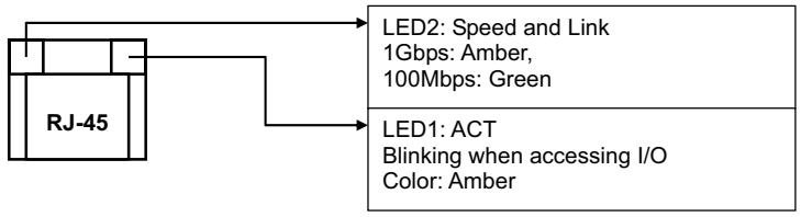
GbE LED
![Based on the provided image, here is the accurate description of the blocks and connections:\n\n**Labeled Blocks:**\n*   **RJ-45**: A schematic of an RJ-45 connector on the left.\n*   **LED2: Speed and Link**: The top section of the box on the right. Inside this block, the text reads:\n    *   1Gbps: Amber,\n    *   100Mbps: Green\n*   **LED1: ACT**: The bottom section of the box on the right. Inside this block, the text reads:\n    *   Blinking when accessing I/O\n    *   Color: Amber\n\n**Connections:**\n*   An arrow connects the top pin of the **RJ-45** block to the **LED2: Speed and Link** block.\n*   An arrow connects the middle pin of the **RJ-45** block to the **LED1: ACT** block.](.atca-6900-50-1g009-1030-204-en/3d0700d1685bf1107582357d1b5aefbff2feeaad264c67328986ed07e5c4625b.jpg)

# 2.9 Compliance

The aTCA-6900 conforms to the following specifications:

▶ PCIMG 3.0 R2.0 ECN0001 AdvancedTCA
▶ PICMG 3.1 Ethernet over AdvancedTCA option 1 and 9
▶ AMC.0 Advanced Mezzanine Card R2.0 Midsize
▶ AMC.1 PCI Express R1.0
▶ AMC.2 E2 / Type 3
▶ AMC.3 Storage R1.0

This page intentionally left blank.

# 3 Functional Description

# 3.1 CPU, Memory and Chipset

CPU

# Two Dual-Core Intel® LV 5138 Processors

The aTCA-6900 supports two Dual-Core Intel® LV-5138 processors at 2.13GHz with 1066MHz FSB and 4MB L2 cache. The Dual-Core Intel® Xeon® Processor 5100 Series are 64-bit server processors utilizing two Intel microarchitecture cores. These processors are based on Intel's 65 nanometer process technology combining high performance with the power efficiencies of a low-power microarchitecture. Some key features include on-die, 32 KB Level 1 instruction and data caches and 4 MB Level 2 cache with Advanced Transfer Cache Architecture. The processors' Data Prefetch Logic speculatively fetches data to the L2 cache before an L1 cache requests occurs, resulting in reduced bus cycle penalties and improved performance. The 1066 MHz Front Side Bus (FSB) is a quad-pumped bus running off a 266 MHz system clock making 8.5 GBytes per second data transfer rates possible.

Enhanced thermal and power management capabilities are implemented including Thermal Monitor (TM1), Thermal Monitor 2 (TM2) and Enhanced Intel SpeedStep® Technology. These technologies are targeted for dual processor in enterprise environments. TM1 and TM2 provide efficient and effective cooling in high temperature situations. Enhanced Intel SpeedStep® Technology provides power management capabilities to servers and workstations.

The Dual-Core Intel® Xeon® Processor LV-5138 features include Advanced Dynamic Execution, enhanced floating point and multi-media units, Streaming SIMD Extensions 2 (SSE2) and Streaming SIMD Extensions 3 (SSE3). Advanced Dynamic Execution improves speculative execution and branch prediction internal to the processor. The floating point and multi-media units include 128-bit wide registers and a separate register for data movement. SSE3 instructions provide highly efficient double-precision floating point, SIMD integer, and memory management operations. It also supports Intel® Extended Memory 64 Technology (Intel® EM64T) as an enhancement to Intel's IA-32 architecture. This enhancement allows the processor to execute operating systems and applications written to take advantage of the 64-bit extension technology.

# Two Quad-Core Intel® L5408 Processors

In addition to two Dual-Core LV-5138 processors, the aTCA-6900 also supports two Quad-Core Intel L5408 Xeon processors. The Quad-Core Intel® Xeon® Processor L5408 is a server processor utilizing four 45-nm Hi-k next generation Intel® Core™ microarchitecture cores. The processor is manufactured on Intel's 45 nanometer process technology combining high performance with the power efficiencies of a low-power microarchitecture. Some key features include on-die, primary 32-kB instruction cache and 32-kB write-back data cache in each core and 12 MB (2 x 6MB) Level 2 cache with Intel® Advanced Smart Cache Architecture. The processors' Data Prefetch Logic speculatively fetches data to the L2 cache before an L1 cache requests occurs, resulting in reduced effective bus latency and improved performance. The 1066 MHz Front Side Bus (FSB) is a quad-pumped bus running off a 266 MHz system clock making 8.5 GBytes per second data transfer rates possible.

Enhanced thermal and power management capabilities are implemented including Intel® Thermal Monitor (TM1), Thermal Monitor 2 (TM2) and Enhanced Intel SpeedStep® Technology. These technologies are targeted for dual processor configurations in enterprise environments. TM1 and TM2 provide efficient and effective cooling in high temperature situations. Enhanced Intel SpeedStep Technology provides power management capabilities to servers and workstations.

Quad-Core Intel® Xeon® Processor L5408 features include Intel® Wide Dynamic Execution, enhanced floating point and multi-media units, Streaming SIMD Extensions 2 (SSE2), Streaming SIMD Extensions 3 (SSE3), and Streaming SIMD Extensions 4.1 (SSE4.1). Advanced Dynamic Execution improves speculative execution and branch prediction internal to the processor. The floating point and multi-media units include 128-bit wide registers and a separate register for data movement. SSE3 instructions provide highly efficient double-precision floating point, SIMD integer, and memory management operations.

It also supports Intel® 64 Architecture as an enhancement to Intel's IA-32 architecture. This enhancement allows the processor to execute operating systems and applications written to take advantage of the 64-bit extension technology.

# Supported Processors, Maximum Power Dissipation

The following tables describe the processors supported on the aTCA-6900 and their maximum power dissipation.

<table><tr><td></td><td>Intel® LV 5138</td><td>Intel® L5408</td></tr><tr><td>L2 cache</td><td>4MB</td><td>12MB</td></tr><tr><td>Clock</td><td>2.13GHz</td><td>2.13GHz</td></tr><tr><td>FSB</td><td>1066MHz</td><td>1066MHz</td></tr></table>

# Memory

The aTCA-6900 supports DDR2-667 RDIMM in four sockets up to 32GBytes. The available COTS DDR2-667 RDIMM densities are 1 GB, 2GB, 4GB and 8GB.

![The image displays a digital icon of a white document sheet with a folded top-right corner and faint horizontal gray lines running across the page. A large, bold red checkmark is superimposed diagonally over the document, extending from the bottom left to the top right.](.atca-6900-50-1g009-1030-204-en/5df12aa2fe7ff6c488d055b5f9807e35206f19a95c3c4d5bceb6d6b1cba8db14.jpg)
NOTE:

Memory configuration changes can only be performed at the factory. Failure to comply with the above may result in damage to your board or improper operation.

# Chipset

# Intel® 5100/ICH9R Chipset Overview

The Intel® 5100 Memory Controller Hub Chipset (code-named San Clemente) is designed for systems based on the Dual-Core Intel® Xeon® processor 5100 series and Quad-Core Intel® Xeon® processor 5400 series, and supports FSB operation of 1066 MT/s. The Intel® 5100 MCH Chipset-based platforms contain two main components: the Memory Controller Hub (MCH) for the host bridge and Intel® 82801IR I/O Controller Hub (ICH9R) for the I/O subsystem.

In an Intel® 5100 MCH Chipset-based platform, the MCH provides two FSB processor interfaces, two DDR2 memory channels, six x4 PCI Express bus interfaces configurable to form x4, x8 or x16 ports, an Enterprise South Bridge Interface (ESI), and three SMBus interfaces for system management, PCI Hot Plug control and DIMM Serial Presence Detect (SPD). The Intel® 5100 Memory Controller Hub Chipset device has DMA Engine (Crystal Beach) capabilities and supports Intel® I/O Acceleration Technology (Intel® I/OAT). The following System Block Diagram shows a block diagram of an Intel® 5100 MCH Chipset based platform.

![Based on the provided flowchart, here are the labeled blocks and their connections:\n\n**Central Block:**\n*   **Intel® 5100 MCH** (Blue rectangle in the center)\n\n**Top Connections:**\n*   **Blocks:** Two orange ovals labeled **Intel® Xeon® LV & LV ATCA Processors**.\n*   **Connection:** Red double-headed arrows connect the central block to each processor.\n*   **Label:** **DIB FSB 1066/1333** is written between the processors and the central block.\n\n**Right Connections:**\n*   **Blocks:** Two stacks of green rectangles labeled **DDR2 533/667**.\n*   **Connection:** Green double-headed arrows connect the central block to the memory stacks.\n*   **Label:** **x4 PCIe Gen1** is next to blue arrows pointing left towards the central block.\n\n**Bottom Center Connections:**\n*   **Labels:** **x8 x8 x8** (under a group of blue arrows) and **x16** (under a single large blue arrow).\n*   **Connection:** Blue arrows point upwards towards the central **Intel® 5100 MCH** block.\n\n**Bottom Left Connections:**\n*   **Block:** A blue oval labeled **ICH9R**.\n*   **Connection:** A blue arrow labeled **x4 ESI** points upwards from the ICH9R block to the central **Intel® 5100 MCH** block.\n*   **Associated Labels:**\n    *   **12 USB 2.0 Ports** and **6 SATA Ports** point towards the ICH9R block.\n    *   **6 x1 Gen1 PCIe* Ports** has an arrow pointing downwards away from the ICH9R block.](.atca-6900-50-1g009-1030-204-en/23ad1f7236106b45cbdb64fb437d2d4f31246b8c8028f432a7315e2d5d3edf10.jpg)

Configurable set of PCI Express\* x4, x8 or x16 ports

The ICH9R is an I/O controller hub supporting various I/O interfaces including six PCI Express x1 ports, Serial ATA host controllers supporting up to six SATA ports at a speed of 3 Gb/s, twelve external USB 2.0 ports with port disable capability, a System Management Bus interface (SMBus), a Serial Peripheral Interface (SPI) and a Low Pincount bus (LPC) for BIOS and firmware storage. Additionally, the ICH9R contains a PCI Controller supporting up to four Bus Masters (PCI Local Bus Specification, Rev. 2.3 compliant), an integrated 10/100/1000 LAN controller and a dedicated ESI port for communication with the MCH.

The ICH9R component provides the data buffering and arbitration required to ensure that system interfaces operate efficiently and provide the bandwidth necessary to enable the system to obtain peak performance. The ICH9R component is ACPI compliant Suspend to RAM, Suspend to Disk, and Soft-Off power management states. Through the use of the integrated LAN functions, the ICH9R also supports Alert Standard Format for remote management.

# ATI ES1000 Graphics Controller

The aTCA-6900 provides an analog VGA port on the front panel powered by an AMD ES1000 2D graphics controller with the following features:

▶ 32-bit PCI bus (Rev 2.2), 3.3 V with bus mastering support

▶ Support for SPI Serial and Flash Memory video BIOS

▶ One CRT controller capable of supporting two identical simultaneous display paths

▶ Dual integrated DACs for CRT display support

▶ Support for external TMDS transmitter via 24-bit digital output to drive most popular TMDS transmitters up to 165MHz frequency

▶ Independent DDC lines for both DACs and TMDS connections. Also full AppleSense support on DAC connection

▶ Static and dynamic Power Management support (APM as well as ACPI) with full VESA DPMS and Energy Star compliance

▶ Comprehensive testability including full internal scan, memory BIST, I/O xor tree and lddq
▶ Full ACPI 1.0b, OnNow, and IAPC (Instantly Available PC) power management, including PCI power management registers
▶ Bi-endian support for compliance on a variety of processor platforms
▶ Bus mastering of 2D display lists
▶ Triple 10-bit palette DAC supports pixel rates to 350MHz
▶ DDC1 and DDC2 for plug and play monitors
▶ Flexible memory support:
▶ DDR1 and DDR2 SDRAM and SGRAM
▷ 16-bit interface
▷ 8MB to 256MB
▶ Up to 1GB/s bandwidth.
▶ Single chip solution in 0.13 micron process, 1.2V CMOS technology in a BGA package

# 3.2 Peripherals

The following standard peripherals are available on the aTCA-6900 blade:

# Timer

The aTCA-6900 is equipped with the following timers:

Real-Time Clock: The IICH contains a real-time clock that performs timekeeping functions and includes 256 bytes of general purpose battery-backed CMOS RAM. Features include an alarm function, programmable periodic interrupt and a 100-year calendar. All battery-backed CMOS RAM data remains stored in an additional EEPROM. This prevents data loss in case the aTCA-6900 is operated without battery.

Counter/Timer: Three 8254-style counter/timers are included on the aTCA-6900 as defined for the PC/AT (System Timer, Refresh Request, Speaker Tone Output).

In addition to the three 8254-style counters, the IICH includes three High Precision Event Timers (HPET) that may be used by the operating system. They are implemented as a single counter each with its own comparator and value register. They support One-shot and periodic interrupts.

# Watchdog Timer

The aTCA-6900 provides a Watchdog Timer that is programmable for a timeout period ranging from 1 to 255 minutes in the minute mode, or 1 to 255 seconds in the second mode. Please refer to “section 6 Watchdog Timer” for detail programming guide.

# Battery

The aTCA-6900 is provided with a 3.0 V “coin cell” lithium battery for the RTC. To replace the battery, proceed as follows:

▶ Turn off power
▶ Remove the battery
▶ Place the new battery in the socket

Make sure that you insert the battery with the correct orientation. The positive pole must be on the top

The lithium battery must be replaced with an identical battery or a battery type recommended by the manufacturer. A suitable battery is the PANASONIC CR2032.

![The image displays a digital icon of a white document or piece of paper featuring horizontal gray lines, resembling a list or notepad. The top-right corner of the paper is folded down. Superimposed over the document is a large, bold, red checkmark.](.atca-6900-50-1g009-1030-204-en/e7ceb813f1071226cd218fb33bc3b15c15551b97f9d0780e4611254f961e16ac.jpg)
NOTE:

The user must be aware that the battery's operational temperature range is less than that of the aTCA-6900's storage temperature range. For exact range information, refer to the battery manufacturer's specifications.

![The image shows a document icon featuring a white page with horizontal gray lines and a folded top-right corner. A large red checkmark is superimposed over the center of the document.](.atca-6900-50-1g009-1030-204-en/07ef689a1ba41dd9be0de0dc11eb96dab3af7cc5ee69cdfd7c15206341d1e0ae.jpg)
NOTE:

Care must be taken to ensure that the battery is correctly replaced. The battery should be replaced only with an identical or equivalent type recommended by the manufacturer. Dispose of used batteries according to the manufacturer's instructions. The typical life expectancy of a 225mAh battery is 4-5 years with an average on-time of 8 hours per working day at an operating temperature of 30°C. However, this typical value varies considerably because the life expectancy is dependent on the operating temperature and standby (shutdown) time of the system in which it operates. To ensure that the lifetime of the battery has not been exceeded, it is recommended to change the battery after 3-4 years.

# Reset

The aTCA-6900 is automatically reset by a precision voltage monitoring circuit that detects a drop in voltage below the acceptable operating limit of 4.85V for the 5V line and below 3.2V for the 3.3V line. Other reset sources include the Watchdog Timer, the face plate push-button switch and also the RESET signal from the IPMC. The aTCA-6900 responds to any of these sources by initializing local peripherals.

A reset will be generated by the following conditions:

▶ Power failure, +5 V supply falls below 4.1 V (typ.) or +3.3 V supply falls below 2.93 V (typ.)
▶ Pushbutton 'RESET" pressed
▶ Watchdog time-out
▶ IPM controller reset

# SMBus and I2C Devices

The aTCA-6900 provides a system management bus (SMBus) hosted by the ICH9R and an I2C bus hosted by the IPM controller, H8S/2168, as shown in the following diagram. The following table describes the function and address of the devices.

![Based on the provided flowchart, here are the labeled blocks and their connections:\n\n**Labeled Blocks:**\n*   **San Clemente** (containing 'Slave' and 'Master')\n*   **ICH9R Master** (containing 'Master')\n*   **CPU XDP**\n*   **MCH XDP**\n*   **BCM56312** (red text: '98')\n*   **Super I/O** (red text: '48')\n*   **CK505** (red text: 'C0')\n*   **DB803** (red text: 'DC')\n*   **Ch0 DIMM A0** (red text: 'A0')\n*   **Ch0 DIMM A1** (red text: 'A2')\n*   **Ch1 DIMM B0** (red text: 'A0')\n*   **Ch1 DIMM B1** (red text: 'A2')\n*   **H8S/2167V** (containing pins: 'SDA4 SCL4', 'SDA3 SCL3', 'SDA2 SCL2', 'SDA0 SCL0', 'SDA5 SCL5')\n*   **CPU0 Sensor(MAX6621)** (red text: '92')\n*   **CPU1 Sensor(MAX6621)** (red text: '90')\n*   **AT24C256** (red text: 'A8')\n*   **LM75** (red text: '9E')\n*   **PCA9555PW** (red text: '48')\n*   **PCA9557PW** (red text: '30')\n*   **ZONE1 IPMB_B**\n*   **ZONE1 IPMB_A**\n*   **Intel 82571EB**\n*   **Intel 82571EB**\n*   **1st AMC** (red text: '72')\n*   **2nd AMC** (red text: '74')\n*   **RTM** (red text: 'C0')\n\n**Connections:**\n*   **ICH9R Master** connects via a line labeled **ICH_SMB** to **San Clemente**.\n*   **ICH9R Master** connects via another line labeled **ICH_SMB** to a vertical bus connecting: **CPU XDP**, **MCH XDP**, **BCM56312** (98), **Super I/O** (48), **CK505** (C0), and **DB803** (DC).\n*   **San Clemente** (Slave, Master) connects via a line labeled **DIML_SMB** to a vertical bus connecting: **Ch0 DIMM A0** (A0), **Ch0 DIMM A1** (A2), **Ch1 DIMM B0** (A0), and **Ch1 DIMM B1** (A2).\n*   **H8S/2167V** connects via pins **SDA4 SCL4** to a vertical bus (labeled **DC_IPM**) connecting: **CPU0 Sensor(MAX6621)** (92), **CPU1 Sensor(MAX6621)** (90), **AT24C256** (A8), **LM75** (9E), **PCA9555PW** (48), and **PCA9557PW** (30).\n*   **H8S/2167V** connects via pins **SDA3 SCL3** to **ZONE1 IPMB_B**.\n*   **H8S/2167V** connects via pins **SDA2 SCL2** to **ZONE1 IPMB_A**.\n*   **H8S/2167V** connects via pins **SDA0 SCL0** to the two **Intel 82571EB** blocks.\n*   **H8S/2167V** connects via pins **SDA5 SCL5** (line labeled **IPMB_L_1**) to **1st AMC** (72).\n*   **1st AMC** (72) connects to **2nd AMC** (74).\n*   **2nd AMC** (74) connects to **RTM** (C0).](.atca-6900-50-1g009-1030-204-en/56e55150acfb4c7c283185fc41c8f8724127ad27e3128550d09c282778d3c9e1.jpg)

<table><tr><td>SMBus Device</td><td>Address (hex)</td><td>I2C Device</td><td>Address (hex)</td></tr><tr><td>DDR2-A0</td><td>10100010(A2)</td><td>CPU0 sensor</td><td>10010010(92)</td></tr><tr><td>DDR2-A1</td><td>10100000(A0)</td><td>CPU1 sensor</td><td>10010000(90)</td></tr><tr><td>DDR2-B0</td><td>10101010(AA)</td><td>External FRU</td><td>10100110(A6)</td></tr><tr><td>DDR2-B1</td><td>10101000(A8)</td><td>LM75</td><td>10011110(9E)</td></tr><tr><td>BCM56312</td><td>10001000(88)</td><td>PCA9555PW</td><td>01000000(40)</td></tr><tr><td>Super IO</td><td>01001000(48)</td><td>PCA9557PW</td><td>00110000(30)</td></tr><tr><td>Clock Gen</td><td>11010010(D2)</td><td></td><td></td></tr><tr><td>Clock Buffer</td><td>11011100(DC)</td><td></td><td></td></tr></table>

# GPIO List

The following table summarizes GPIO usage on ICH9R IO controller hub:

<table><tr><td>ICH9R</td><td>I/O</td><td>Signal</td><td>Description</td></tr><tr><td>GPI[0]</td><td>Input</td><td>LPC_PME-L</td><td>LPC power management event</td></tr><tr><td>GPI[8]</td><td>Input</td><td>ICH_GPIO8</td><td>Debug from MCH ERR-L1</td></tr><tr><td>GPI[10]</td><td>Input</td><td>ICH_GPIO10</td><td>Debug from MCH ERR-L2</td></tr><tr><td>GPO[15]</td><td>Output</td><td>PCI_STOP-L</td><td>PCI stop to clock generator</td></tr><tr><td>GPI[19]</td><td>Input</td><td>3255_INT_REQ1</td><td>Interrupt request 1 from IDT82V3255</td></tr><tr><td>GPI[21]</td><td>Input</td><td>3255_INT_REQ2</td><td>Interrupt request 2 from IDT82V3255</td></tr><tr><td>GPI[22]</td><td>Input</td><td>LPC_SMI-L</td><td>LPC system management interrupt from IPMC</td></tr><tr><td>CPO[25]</td><td>Output</td><td>CLK_CPU_STOP-L</td><td>CPU stop to clock generator</td></tr><tr><td>GPO[32]</td><td>Output</td><td>POSTOK-L</td><td>POST OK to IPMC</td></tr><tr><td>GPO[34]</td><td>Output</td><td>USERLED</td><td>User defined LED, default = Power LED</td></tr><tr><td>GPI[38]</td><td>Input</td><td>ICH_GPIO38</td><td>Debug from MCH ERR-L10</td></tr><tr><td>GPO[39]</td><td>Output</td><td>ICH_CPU0_FORCEPR-L</td><td>CPU0 forced protection</td></tr><tr><td>GPO[48]</td><td>Output</td><td>ICH_CPU1_FORCEPR-L</td><td>CPU1 forced protection</td></tr><tr><td>GPI[57]</td><td>Input</td><td>W83627_OVT-L</td><td>W83627 over-temperature event</td></tr><tr><td>GPO[58]</td><td>Output</td><td>3255_CS-L2</td><td>Chip select to IDT82V3255</td></tr></table>

# 3.3 I/O Interfaces

# USB

The aTCA-6900 supports eight USB 2.0 ports:

▶ three Type-A ports on front panel
▶ four ports routed to RTM
▶ one channel for 4GB on-board NAND flash

On the USB 2.0 front panel port, a USB cable with up to 5 meters in length can be used.

On the USB 2.0 Rear I/O ports, it is strongly recommended to use a cable below 3 meters in length for USB 2.0 devices.

The USB 2.0 ports are high-speed, full-speed, and low-speed capable. Hi-speed USB 2.0 allows data transfers of up to 480 Mb/s, 40 times faster than a full-speed USB (USB 1.1). One USB peripheral may be connected to each port.

Front Panel USB Connector (CN9-11)

<table><tr><td>Pin #</td><td>Signal Name</td></tr><tr><td>1</td><td>Vcc</td></tr><tr><td>2</td><td>UV0-</td></tr><tr><td>3</td><td>UV0+</td></tr><tr><td>4</td><td>GND</td></tr></table>

![A black and white line drawing depicts a rectangular electrical connector, likely a USB Type-A. The diagram shows a large outer rectangle containing a central rectangular housing. Inside this housing, four smaller rectangular contacts are arranged in a vertical column. On the right side of the diagram, the number '4' is located near the top and the number '1' is located near the bottom, positioned between two vertical lines.](.atca-6900-50-1g009-1030-204-en/c9c24374b8427cb07487029815785a976e3f4ab8e266dfcd4f64a4bec55bf53c.jpg)
Table 3-1: Front Panel USB Connector Pin Definition

![An icon depicting a white document with faint horizontal lines and a folded top-right corner, overlaid with a large red checkmark.](.atca-6900-50-1g009-1030-204-en/a81ac8a0411e9fc26a7f5adf6ff2e9a2008b5440734a909547cc92cf8be57ab7.jpg)
NOTE:

The aTCA-6900 host interfaces can be used with maximum 500mA continuous load current as specified in the Universal Serial Bus Specification, Revision 2.0. Short circuit protection is provided. All the signal lines are EMI filtered.

# VGA Analog Interface

The DB-15 female connector CN15 is for analog display output.

DB-15 VGA Connector (CN15)

<table><tr><td>Signal Name</td><td>Pin #</td><td>Pin #</td><td>Signal Name</td></tr><tr><td>Red</td><td>1</td><td>2</td><td>Green</td></tr><tr><td>Blue</td><td>3</td><td>4</td><td>N.C.</td></tr><tr><td>GND</td><td>5</td><td>6</td><td>GND</td></tr><tr><td>GND</td><td>7</td><td>8</td><td>GND</td></tr><tr><td>+5V.</td><td>9</td><td>10</td><td>GND</td></tr><tr><td>N.C.</td><td>11</td><td>12</td><td>DDC_DATA</td></tr><tr><td>HSYNC</td><td>13</td><td>14</td><td>VSYNC</td></tr><tr><td>DDC_CLK</td><td>15</td><td></td><td></td></tr></table>

![6\n1\n11\n5\n15\n10](.atca-6900-50-1g009-1030-204-en/50f5a97a6fff7cb1ce80dd83f73aa51a54f87b9fd52b240e272bfa499824bd07.jpg)

Table 3-2: VGA Connector Pin Definition

# Gigabit Ethernet

# aTCA-6900

The standard aTCA-6900 contains two Intel® 82571EB Dual Gigabit Ethernet controllers, which provide a total of four 10/100/1000Base-T ports onboard. In default configuration, two of them are connected to the front panel and the other two are connected to the Base Interface channels.

![**Blocks:**\n*   **Fabric Riser Card (FRC)** (Orange): Contains text 'aDB-6900-A' and 'Intel 82598EB'.\n*   **Intel® 82571EB** (Blue, Left): Contains sub-blocks labeled 'Copper' and 'SerDes'.\n*   **Intel® 82571EB** (Blue, Right): Contains sub-blocks labeled 'Copper' and 'SerDes'.\n*   **AMC #1** (Orange, Left).\n*   **AMC #2** (Orange, Left).\n*   **BCM56312** (Grey, Center): Contains text 'GbEx24' and '10GbEx2'.\n*   **BCM5464** (Grey, Top Right).\n*   **BCM5464** (Grey, Bottom).\n*   **ZONE2** (Orange, Far Right, vertical).\n\n**Connections:**\n*   **Fabric Riser Card (FRC)** connects to **ZONE2** via a solid line labeled **FCH1/FCH2**.\n*   **Fabric Riser Card (FRC)** connects to **BCM56312** via two dashed vertical lines labeled **10GbE x 2** and **GbE x 2**.\n*   **Intel® 82571EB (Left)** connects outward to the left via solid lines with arrows labeled **GbE x2 to Front Panel**. It connects via dashed lines to **BCM56312**.\n*   **Intel® 82571EB (Right)** connects to **ZONE2** via a solid line labeled **BCH1/BCH2**. It connects via dashed lines to **BCM56312**.\n*   **BCM56312** connects to **AMC #1** via a grey leftward arrow labeled **AMC.2 E2/T3**.\n*   **BCM56312** connects to **AMC #2** via a grey leftward arrow labeled **AMC.2 E2/T3**.\n*   **BCM56312** connects to **BCM5464** (Top Right) via a dashed horizontal line.\n*   **BCM56312** connects to **BCM5464** (Bottom) via a dashed vertical line.\n*   **BCM5464** (Bottom) connects outward to the left via dashed arrows labeled **GbE x2 to Front Panel**.\n*   **BCM56312** connects outward to the right via a dashed arrow labeled **GbE x2 to RTM**.](.atca-6900-50-1g009-1030-204-en/1cfef8dbc8326ef0a6241aed55078a147fca01a5836ff76bf3998887af635eaa.jpg)

Figure 3-1: Standard aTCA-6900 GbE Configuration

# aTCA-6900S

In the aTCA-6900S with built-in BCM56312 switch, the 82571EB controllers will work in SERDES mode providing the ports to the onboard BCM56312 24-port layer 3 switch. The port mapping in this configuration is shown in the table below.

The Fabric Riser Card (FRC) provides the capability to support different configurations for FCH1 and FCH2. An aDB-6900-A FRC is installed on both the aTCA-6900 and aTCA-6900S by default. The Intel 82598EB Ethernet controller connects to the MCH via a PCI-E x8 interface and provides 10GbE link to FCH1 and FCH2.

<table><tr><td>Port</td><td>Connection</td><td>Port</td><td>Connection</td></tr><tr><td>0</td><td>82571EB port 0</td><td>10-11</td><td>AMC#1 port 0/1</td></tr><tr><td>1</td><td>82571EB port 1</td><td>12-14</td><td>AMC#1 port 8-10</td></tr><tr><td>2</td><td>N/A</td><td>15</td><td>FRC port 0</td></tr><tr><td>3</td><td>N/A</td><td>16-17</td><td>RTM port 0/1</td></tr><tr><td>4-5</td><td>Egress GbE 1/2</td><td>18-19</td><td>AMC#2 port 0/1</td></tr><tr><td>6-7</td><td>N/A</td><td>20-22</td><td>AMC#2 port 8-10</td></tr><tr><td>8-9</td><td>N/A</td><td>23</td><td>FRC port 1</td></tr></table>

Table 3-3: aTCA-6900S GbE Configuration

![Based on the provided flowchart, here are the labeled blocks and their connections:\n\n**Labeled Blocks:**\n*   **Fabric Riser Card (FRC)** (containing 'aDB-6900-A' and 'Intel 82598EB')\n*   **Intel® 82571EB** (containing 'Copper' and 'SerDes') - appearing twice (left and right)\n*   **AMC #1**\n*   **AMC #2**\n*   **BCM56312 GbEx24 10GbEx2** (central blue block)\n*   **BCM5464** (appearing twice: one on the right, one at the bottom)\n*   **ZONE2** (tall vertical bar on the far right)\n\n**Connections:**\n*   **Fabric Riser Card (FRC)** connects to **BCM56312 GbEx24 10GbEx2** via red lines labeled '**10GbE x 2**' and white lines labeled '**GbE x 2**'.\n*   **Fabric Riser Card (FRC)** connects to **ZONE2** via a line labeled '**FCH1/FCH2**'.\n*   **Intel® 82571EB** (left) connects to **BCM56312 GbEx24 10GbEx2**.\n*   **Intel® 82571EB** (right) connects to **BCM56312 GbEx24 10GbEx2**.\n*   **BCM56312 GbEx24 10GbEx2** connects to **AMC #1** via a double-headed arrow labeled '**AMC.2 E2/T3**'.\n*   **BCM56312 GbEx24 10GbEx2** connects to **AMC #2** via a double-headed arrow labeled '**AMC.2 E2/T3**'.\n*   **BCM56312 GbEx24 10GbEx2** connects to **BCM5464** (bottom) via two vertical lines.\n*   **BCM56312 GbEx24 10GbEx2** connects to **ZONE2** via an arrow labeled '**GbE x2 to RTM**'.\n*   **Intel® 82571EB** (right) connects to **ZONE2** via a line labeled '**BCH1/BCH2**'.\n*   **BCM5464** (bottom) connects outward via double-headed arrows labeled '**GbE x2 to Front Panel**'.\n*   **Intel® 82571EB** (left) connects outward via dashed arrows labeled '**GbE x2 to Front Panel**'.\n*   **BCM56312 GbEx24 10GbEx2**, **Intel® 82571EB** (right), and **BCM56312 GbEx24 10GbEx2** (via dashed lines) connect to **BCM5464** (right) and **ZONE2**.](.atca-6900-50-1g009-1030-204-en/0774ef49f0af4fab03c3f5ed6f070c47fdc944f772e05790421cab0c451d0496.jpg)

Figure 3-2: aTCA-6900S GbE Custom Configuration

# Serial Port

One PC-compatible serial RS-232, RJ45 port is provided on the front panel with DIP switches SWX1 and SWX2 used to set COM function. A complete set of handshaking and modem control signals are supported, with data transfer rates up to 115.2 kB/sec.

The Front Panel RJ45 COM connector CN14 pin-assignment are DIP switch settings are listed below.

COM1 Serial Port Connector (RJ45)

<table><tr><td>Pin #</td><td>Signal</td><td>Function</td></tr><tr><td>1</td><td>DCD#</td><td>Data Carrier Detect</td></tr><tr><td>2</td><td>RTS#</td><td>Request to Send</td></tr><tr><td>3</td><td>DSR#</td><td>Data Set Ready</td></tr><tr><td>4</td><td>TXD</td><td>Transmit Data</td></tr><tr><td>5</td><td>RXD</td><td>Receive Data</td></tr><tr><td>6</td><td>GND</td><td>Ground</td></tr><tr><td>7</td><td>CTS#</td><td>Clear to Send</td></tr><tr><td>8</td><td>DTR#</td><td>Data Terminal Ready</td></tr></table>

![1\n6](.atca-6900-50-1g009-1030-204-en/57b5cfe114740b1a40a1dc041ff8e1cade93b1fa8b97f807b69a2e96d83d0e9d.jpg)

Table 3-4: COM1 Serial Port Connector Pin Definition

COM Mode Switch Settings (SWX1 and SWX2)

<table><tr><td>Mode</td><td>Switch</td><td>Pin 1</td><td>Pin 2</td><td>Pin 3</td><td>Pin 4</td></tr><tr><td rowspan="2">RS-232 (default)</td><td>SWX1</td><td>ON</td><td>ON</td><td>OFF</td><td>OFF</td></tr><tr><td>SWX2</td><td>ON</td><td>OFF</td><td colspan="2">N/A</td></tr><tr><td rowspan="2">IPMC debug port</td><td>SWX1</td><td>OFF</td><td>OFF</td><td>ON</td><td>ON</td></tr><tr><td>SWX2</td><td>OFF</td><td>ON</td><td colspan="2">N/A</td></tr></table>

Table 3-5: COM Mode Switch Settings

![Close-up of an electronic circuit board with a highlighted component (no visible text or symbols)](.atca-6900-50-1g009-1030-204-en/e0485306353d42bfbfc63768772a2ac5440776fcce9227da3d695b175dcb122e.jpg)

Figure 3-3: SWX1 and SWX2 location

When the switch SWX4 is set to IPMC debug port, the pin assignment of the RJ45 connector is as below.

<table><tr><td>Pin #</td><td>Signal</td><td>Function</td></tr><tr><td>1</td><td>NC</td><td>Not connected</td></tr><tr><td>2</td><td>NC</td><td>Not connected</td></tr><tr><td>3</td><td>NC</td><td>No connected</td></tr><tr><td>4</td><td>DBG_TX</td><td>IPMC Transmit Data</td></tr><tr><td>5</td><td>DBG_RX</td><td>IPMC Receive Data</td></tr><tr><td>6</td><td>GND</td><td>Ground</td></tr><tr><td>7</td><td>NC</td><td>No connected</td></tr><tr><td>8</td><td>NC</td><td>No connected</td></tr></table>

Table 3-6: IPMC Debug Port Connector Pin Definition

# 3.4 AMC Bays

The aTCA-6900 provides two PICMG AMC.0 R2.0 single width, mid-size AMC bays, with the following features:

# AMC#1:

▶ AMC.1 PCI Express Type 4 (PCI-E x4 from 5100 MCH)
▶ AMC.2 Gigabit Ethernet E2/Type 3 (from BCM56312)
▶ AMC.3 Storage S2 (port2: SATA from ICH9R, port3: SAS from LSISAS1064E)
▶ TDP: 60W (+12V, 5A, maximum)
▶ 8 contacts allocated to Payload Power
▶ 56 contacts to allocated to Logic Ground
▶ 2 contacts reserved

# AMC#2:

▶ AMC.1 PCI Express Type 1 (port4: PCI-E x1 from ICH9R)
▶ AMC.2 Gigabit Ethernet E2/Type 3 (from BCM56312)
▶ AMC.3 Storage S2 (port2: SATA from ICH9R, port3: SAS from LSISAS1064E)
▶ TDP: 30W (+12V, 2.5A, maximum)

The AMC connector pin assignment is as follows.

![The image displays a white document icon with a folded top-left corner and faint horizontal gray lines across the lower portion. A large red checkmark is superimposed diagonally over the center of the page.](.atca-6900-50-1g009-1030-204-en/c5b05036671a66b7fcc2d38016be11577d311b088445c35f44a01893935b0ff2.jpg)
NOTE:

For AMC#2, pins 50, 51, 53, 54, 59, 60, 62, 63, 65, 66, 68, 69 are not connected (NC).

<table><tr><td>Pin#</td><td>Signal</td><td>Function</td><td>Pin#</td><td>Signal</td><td>Function</td></tr><tr><td>85</td><td>GND</td><td>Logic Ground</td><td>86</td><td>GND</td><td>Logic Ground</td></tr><tr><td>84</td><td>P12V_PWR</td><td>12V Payload Power</td><td>87</td><td>GE12_RX-</td><td>Port 8 AMC.2 T3 RX-</td></tr><tr><td>83</td><td>PS0#</td><td>Presence 0</td><td>88</td><td>GE12_RX+</td><td>Port 8 AMC.2 T3 RX+</td></tr><tr><td>82</td><td>GND</td><td>Logic Ground</td><td>89</td><td>GND</td><td>Logic Ground</td></tr><tr><td>81</td><td>PCIEREF-</td><td>Fabric Clock A-</td><td>90</td><td>GE12_TX-</td><td>Port8 AMC.2 T3 TX-</td></tr><tr><td>80</td><td>PCIEREF+</td><td>Fabric Clock A+</td><td>91</td><td>GE12_TX+</td><td>Port8 AMC.2 T3 TX+</td></tr><tr><td>79</td><td>GND</td><td>Logic Ground</td><td>92</td><td>GND</td><td>Logic Ground</td></tr><tr><td>78</td><td>AMC_CLKB-N</td><td>Reserved</td><td>93</td><td>GE13_RX-</td><td>Port 9 AMC.2 T3 RX-</td></tr><tr><td>77</td><td>AMC_CLKB-P</td><td>Reserved</td><td>94</td><td>GE13_RX+</td><td>Port 9 AMC.2 T3 RX+</td></tr><tr><td>76</td><td>GND</td><td>Logic Ground</td><td>95</td><td>GND</td><td>Logic Ground</td></tr><tr><td>75</td><td>AMC-CLKA-N</td><td>Reserved</td><td>96</td><td>GE13_TX-</td><td>Port 9 AMC.2 T3 TX-</td></tr><tr><td>74</td><td>AMC-CLKA-P</td><td>Reserved</td><td>97</td><td>GE13_TX+</td><td>Port 9 AMC.2 T3 TX+</td></tr><tr><td>73</td><td>GND</td><td>Logic Ground</td><td>98</td><td>GND</td><td>Logic Ground</td></tr><tr><td>72</td><td>P12V_PWR</td><td>12V Payload Power</td><td>99</td><td>GE14_RX-</td><td>Port 10 AMC.2 T3 RX-</td></tr><tr><td>71</td><td>IPMB_SDA_0</td><td>IPMB-L Data</td><td>100</td><td>GE14_RX+</td><td>Port 10 AMC.2 T3 RX+</td></tr><tr><td>70</td><td>GND</td><td>Logic Ground</td><td>101</td><td>GND</td><td>Logic Ground</td></tr><tr><td>69</td><td>PCIE_MCH_RX3-</td><td>Port 7 RX- for PCIe</td><td>102</td><td>GE14_TX-</td><td>Port 10 AMC.2 T3 TX-</td></tr><tr><td>68</td><td>PCIE_MCH_RX3+</td><td>Port 7 RX+ for PCIe</td><td>103</td><td>GE14_TX+</td><td>Port 10 AMC.2 T3 TX+</td></tr><tr><td>67</td><td>GND</td><td>Logic Ground</td><td>104</td><td>GND</td><td>Logic Ground</td></tr><tr><td>66</td><td>PCIE_MCH_TX3-</td><td>Port 7 TX- for PCIe</td><td>105</td><td>NC</td><td>Not connected</td></tr><tr><td>65</td><td>PCIE_MCH_TX3+</td><td>Port 7 TX+ for PCIe</td><td>106</td><td>NC</td><td>Not connected</td></tr><tr><td>64</td><td>GND</td><td>Logic Ground</td><td>107</td><td>GND</td><td>Logic Ground</td></tr><tr><td>63</td><td>PCIE_MCH_RX2-</td><td>Port 6 RX- for PCIe</td><td>108</td><td>NC</td><td>Not connected</td></tr><tr><td>62</td><td>PCIE_MCH_RX2+</td><td>Port 6 RX+ for PCIe</td><td>109</td><td>NC</td><td>Not connected</td></tr><tr><td>61</td><td>GND</td><td>Logic Ground</td><td>110</td><td>GND</td><td>Logic Ground</td></tr><tr><td>60</td><td>PCIE_MCH_TX2-</td><td>Port 6 TX- for PCIe</td><td>111</td><td>NC</td><td>Not Connected</td></tr><tr><td>59</td><td>PCIE_MCH_TX2+</td><td>Port 6 TX+ for PCIe</td><td>112</td><td>NC</td><td>Not Connected</td></tr><tr><td>58</td><td>GND</td><td>Logic Ground</td><td>113</td><td>GND</td><td>Logic Ground</td></tr><tr><td>57</td><td>P12V_PWR</td><td>12V Payload Power</td><td>114</td><td>NC</td><td>Not Connected</td></tr><tr><td>56</td><td>IPMB_SCL_0</td><td>IPMB-L Clock</td><td>115</td><td>NC</td><td>Not Connected</td></tr><tr><td>55</td><td>GND</td><td>Logic Ground</td><td>116</td><td>GND</td><td>Logic Ground</td></tr></table>

Table 3-7: AMC Connector Pin Assignment

<table><tr><td>Pin#</td><td>Signal</td><td>Function</td><td>Pin#</td><td>Signal</td><td>Function</td></tr><tr><td>54</td><td>PCIE_MCH_RX1-</td><td>Port 5 RX- for PCIe</td><td>117</td><td>RTM_IO13_TX-</td><td>RTMIO13 TX-</td></tr><tr><td>53</td><td>PCIE_MCH_RX1+</td><td>Port 5 RX+ for PCIe</td><td>118</td><td>RTM_IO13_TX+</td><td>RTMIO13 TX+</td></tr><tr><td>52</td><td>GND</td><td>Logic Ground</td><td>119</td><td>GND</td><td>Logic Ground</td></tr><tr><td>51</td><td>PCIE_MCH_TX1-</td><td>Port 5 TX- for PCIe</td><td>120</td><td>RTM_IO13_RX-</td><td>RTMIO13 RX-</td></tr><tr><td>50</td><td>PCIE_MCH_TX1+</td><td>Port 5 TX+ for PCIe</td><td>121</td><td>RTM_IO13_RX+</td><td>RTMIO13 RX+</td></tr><tr><td>49</td><td>GND</td><td>Logic Ground</td><td>122</td><td>GND</td><td>Logic Ground</td></tr><tr><td>48</td><td>PCIE_MCH_RX0-</td><td>Port 4 RX- for PCIe</td><td>123</td><td>RTM_IO14_TX-</td><td>RTMIO14 TX-</td></tr><tr><td>47</td><td>PCIE_MCH_RX0+</td><td>Port 4 RX+ for PCIe</td><td>124</td><td>RTM_IO14_TX+</td><td>RTMIO14 TX+</td></tr><tr><td>46</td><td>GND</td><td>Logic Ground</td><td>125</td><td>GND</td><td>Logic Ground</td></tr><tr><td>45</td><td>PCIE_MCH_TX0-</td><td>Port 4 TX- for PCIe</td><td>126</td><td>RTM_IO14_RX-</td><td>RTMIO14 RX-</td></tr><tr><td>44</td><td>PCIE_MCH_TX0+</td><td>Port 4 TX+ for PCIe</td><td>127</td><td>RTM_IO14_RX+</td><td>RTMIO14 RX+</td></tr><tr><td>43</td><td>GND</td><td>Logic Ground</td><td>128</td><td>GND</td><td>Logic Ground</td></tr><tr><td>42</td><td>P12V_PWR</td><td>12V Payload Power</td><td>129</td><td>RTM_IO15_TX-</td><td>RTMIO15 TX-</td></tr><tr><td>41</td><td>ENABLE-#</td><td>AMC Enable</td><td>130</td><td>RTM_IO15_TX+</td><td>RTMIO15 TX+</td></tr><tr><td>40</td><td>GND</td><td>Logic Ground</td><td>131</td><td>GND</td><td>Logic Ground</td></tr><tr><td>39</td><td>SAS1_RX1-</td><td>Port 3 RX- for SAS P1</td><td>132</td><td>RTM_IO15_RX-</td><td>RTMIO15 RX-</td></tr><tr><td>38</td><td>SAS1_RX1+</td><td>Port 3 RX+ for SAS P1</td><td>133</td><td>RTM_IO15_RX+</td><td>RTMIO15 RX+</td></tr><tr><td>37</td><td>GND</td><td>Logic Ground</td><td>134</td><td>GND</td><td>Logic Ground</td></tr><tr><td>36</td><td>SAS1_TX1-</td><td>Port 3 TX- for SAS P1</td><td>135</td><td>NC</td><td>Not Connected</td></tr><tr><td>35</td><td>SAS1_TX1+</td><td>Port 3 TX+ for SAS P1</td><td>136</td><td>NC</td><td>Not Connected</td></tr><tr><td>34</td><td>GND</td><td>Logic Ground</td><td>137</td><td>GND</td><td>Logic Ground</td></tr><tr><td>33</td><td>SATA1_RX0-</td><td>Port 2 RX- for SATA P1</td><td>138</td><td>NC</td><td>Not Connected</td></tr><tr><td>32</td><td>SATA1_RX0+</td><td>Port 2 RX+ for SATA1</td><td>139</td><td>NC</td><td>Not Connected</td></tr><tr><td>31</td><td>GND</td><td>Logic Ground</td><td>140</td><td>GND</td><td>Logic Ground</td></tr><tr><td>30</td><td>SATA_TX0-</td><td>Port 2 TX- for SATA</td><td>141</td><td>RTM_IO17_TX-</td><td>RTMIO17 TX-</td></tr><tr><td>29</td><td>SATA_TX0+</td><td>Port 2 TX+ for SATA</td><td>142</td><td>RTM_IO17_TX+</td><td>RTMIO17 TX+</td></tr><tr><td>28</td><td>GND</td><td>Logic Ground</td><td>143</td><td>GND</td><td>Logic Ground</td></tr><tr><td>27</td><td>P12V_PWR</td><td>12V Payload Power</td><td>144</td><td>RTM_IO17_RX-</td><td>RTMIO17 RX-</td></tr><tr><td>26</td><td>GA2</td><td>Geographic Addr. 2</td><td>145</td><td>RTM_IO17_RX+</td><td>RTMIO17 RX+</td></tr><tr><td>25</td><td>GND</td><td>Logic Ground</td><td>146</td><td>GND</td><td>Logic Ground</td></tr><tr><td>24</td><td>LAN_A_SRDS_RXB-</td><td>Port 1 RX- for GbE</td><td>147</td><td>RTM_IO18_TX-</td><td>RTMIO18 TX-</td></tr></table>

Table 3-6: AMC Module Connector Pin Assignment (cont'd)

<table><tr><td>Pin#</td><td>Signal</td><td>Function</td><td>Pin#</td><td>Signal</td><td>Function</td></tr><tr><td>23</td><td>LAN_A_SRDS_RXB+</td><td>Port 1 RX+ for GbE</td><td>148</td><td>RTM_IO18_TX+</td><td>RTMIO18 TX+</td></tr><tr><td>22</td><td>GND</td><td>Logic Ground</td><td>149</td><td>GND</td><td>Logic Ground</td></tr><tr><td>21</td><td>LAN_A_SRDS_TXB-</td><td>Port 1 TX- for GbE</td><td>150</td><td>RTM_IO18_RX-</td><td>RTMIO18 RX-</td></tr><tr><td>20</td><td>LAN_A_SRDS_TXB+</td><td>Port 1 TX+ for GbE</td><td>151</td><td>RTM_IO18_RX+</td><td>RTMIO18 RX+</td></tr><tr><td>19</td><td>GND</td><td>Logic Ground</td><td>152</td><td>GND</td><td>Logic Ground</td></tr><tr><td>18</td><td>P12V_PWR</td><td>12V Payload Power</td><td>153</td><td>RTM_IO19_TX-</td><td>RTMIO19 TX-</td></tr><tr><td>17</td><td>GA1</td><td>Geographic Addr.1</td><td>154</td><td>RTM_IO19_TX+</td><td>RTMIO19 TX+</td></tr><tr><td>16</td><td>GND</td><td>Logic Ground</td><td>155</td><td>GND</td><td>Logic Ground</td></tr><tr><td>15</td><td>LAN_A_SRDS_RXA-</td><td>Port 0 RX- for GbE</td><td>156</td><td>RTM_IO19_RX-</td><td>RTMIO19 RX-</td></tr><tr><td>14</td><td>LAN_A_SRDS_RXA+</td><td>Port 0 RX+ for GbE</td><td>157</td><td>RTM_IO19_RX+</td><td>RTMIO19 RX+</td></tr><tr><td>13</td><td>GND</td><td>Logic Ground</td><td>158</td><td>GND</td><td>Logic Ground</td></tr><tr><td>12</td><td>LAN_A_SRDS_TXA-</td><td>Port 0 TX- for GbE</td><td>159</td><td>RTM_IO20_TX-</td><td>RTMIO20 TX-</td></tr><tr><td>11</td><td>LAN_A_SRDS_TXA+</td><td>Port 0 TX+ for GbE</td><td>160</td><td>RTM_IO20_TX+</td><td>RTMIO20 TX+</td></tr><tr><td>10</td><td>GND</td><td>Logic Ground</td><td>161</td><td>GND</td><td>Logic Ground</td></tr><tr><td>9</td><td>P12V_PWR</td><td>12V Payload Power</td><td>162</td><td>RTM_IO20_RX-</td><td>RTMIO20 RX-</td></tr><tr><td>8</td><td>NC</td><td>Not Connected</td><td>163</td><td>RTM_IO20_RX+</td><td>RTMIO20 RX+</td></tr><tr><td>7</td><td>GND</td><td>Logic Ground</td><td>164</td><td>GND</td><td>Logic Ground</td></tr><tr><td>6</td><td>NC</td><td>Not Connected</td><td>165</td><td>TCK</td><td>JTAG Test Clock Input</td></tr><tr><td>5</td><td>GA0</td><td>Geographic Addr. 0</td><td>166</td><td>TMS</td><td>JTAG Test Mode Select In</td></tr><tr><td>4</td><td>P3V3_MP</td><td>+3.3V Mgmt. Power</td><td>167</td><td>TRST#</td><td>JTAG Test Reset Input</td></tr><tr><td>3</td><td>PS1#</td><td>Presence 1</td><td>168</td><td>TDO</td><td>JTAG Test Data Output</td></tr><tr><td>2</td><td>P12V_PWR</td><td>12V Payload Power</td><td>169</td><td>TDI</td><td>JTAG Test Data Input</td></tr><tr><td>1</td><td>GND</td><td>Logic Ground</td><td>170</td><td>GND</td><td>Logic Ground</td></tr></table>

Table 3-6: AMC Module Connector Pin Assignment (cont'd)

# 3.5 Switches

Switches SW4 and SW5 are for debugging purposes. For normal operation, leave the switches in their default settings.

![Close-up of an electronic circuit board with visible traces and components, no text or symbols present.](.atca-6900-50-1g009-1030-204-en/149b06a6670d69efd2663f04d833778dd3fa949f029a41d96e7aec597b8fe0b1.jpg)

Figure 3-4: SW4 and SW5 location

SW4

<table><tr><td>SW4</td><td>Pin 1</td><td>Pin 2</td><td>Pin 3</td><td>Pin 4</td></tr><tr><td>Default Setting</td><td>ON</td><td>OFF</td><td>ON</td><td>ON</td></tr></table>

▶ Pin 1: N/C
▶ Pin 2: ON for Standalone Mode / OFF for Normal Mode
▶ Pin 3: Reserved
▶ Pin 4: Reserved

SW5

<table><tr><td>SW5</td><td>Pin 1</td><td>Pin 2</td><td>Pin 3</td><td>Pin 4</td></tr><tr><td>Default Setting</td><td>OFF</td><td>OFF</td><td>OFF</td><td>OFF</td></tr></table>

▶ Pin 1: ON for FWE pin protection / OFF for Normal operation
▶ Pin 2: ON for Slave SPI / OFF for Master SPI
▶ Pin 3: IMPC MODE SELECT
▶ Pin 4: ON for Program IPMC / OFF for Normal operation

# Other Switches

Switches SW6, SWZ3 & SWZ4 are not user configurable.

Please leave them in their default settings as below:

SW6

<table><tr><td>SW6 (default)</td><td>Pin 1</td><td>Pin 2</td><td>Pin 3</td><td>Pin 4</td></tr><tr><td>aTCA-6900</td><td>ON</td><td>ON</td><td>ON</td><td>ON</td></tr><tr><td>aTCA-6900S</td><td>OFF</td><td>OFF</td><td>ON</td><td>ON</td></tr></table>

SWZ3

<table><tr><td>SWZ3 (default)</td><td>Pin 1</td><td>Pin 2</td><td>Pin 3</td><td>Pin 4</td></tr><tr><td>aTCA-6900</td><td>ON</td><td>OFF</td><td>ON</td><td>OFF</td></tr><tr><td>aTCA-6900S</td><td>OFF</td><td>ON</td><td>ON</td><td>OFF</td></tr></table>

SWZ4

<table><tr><td>SWZ4 (default)</td><td>Pin 1</td><td>Pin 2</td><td>Pin 3</td><td>Pin 4</td></tr><tr><td>aTCA-6900</td><td>ON</td><td>ON</td><td>ON</td><td>ON</td></tr><tr><td>aTCA-6900S</td><td>OFF</td><td>OFF</td><td>ON</td><td>ON</td></tr></table>

# 4 Hardware Platform Management

# 4.1 Platform Management Overview

The purpose of the hardware platform management system is to monitor, control, and assure proper operation of AdvancedTCA® Boards and other Shelf components. The hardware platform management system watches over the basic health of the system, reports anomalies, and takes corrective action when needed. The hardware platform management system can retrieve inventory information and sensor readings as well as receive event reports and failure notifications from Boards and other Intelligent FRUs. The hardware platform management system can also perform basic recovery operations such as power cycle or reset of managed entities.

The IPMC controller on the aTCA-6900 supports an “intelligent” hardware management system, based on the Intelligent Platform Management Interface Specification. The hardware management system provides the ability to manage the power, cooling, and interconnect needs of intelligent devices; to monitor events; and to log events to a central repository.

# 4.2 IPMI Sensors

Following table lists all the sensors supported by the aTCA-6900.

<table><tr><td>Item</td><td>Sensor Name</td><td>Sensor Address</td><td>Description</td></tr><tr><td>(1)</td><td>Hotswap</td><td>(0x0)</td><td>FRU Hotswap Sensor. Please refer to section 4.2.1</td></tr><tr><td>(2)</td><td>Shelf FRU Hotswap</td><td>(0x1)</td><td>FRU Hotswap Sensor. Please refer to section 4.2.1</td></tr><tr><td>(3)</td><td>Hot Swap AMC 1</td><td>(0x2)</td><td>AMC#1 Hotswap Sensor. Please refer to section 4.2.1</td></tr><tr><td>(4)</td><td>Hot Swap AMC 2</td><td>(0x3)</td><td>AMC#2 Hotswap Sensor. Please refer to section 4.2.1</td></tr><tr><td>(5)</td><td>Hot Swap AMC 3</td><td>(0x4)</td><td>RTM Hotswap Sensor. Please refer to section 4.2.1</td></tr><tr><td>(6)</td><td>+5.0V</td><td>(0x5)</td><td>Voltage Sensor. Please refer to section 4.2.5Upper Non-Recoverable Threshold = 5.5 VoltsUpper Critical Threshold = 5.4 VoltsUpper Non-Critical Threshold = 5.3 VoltsLower Non-Critical Threshold = 4.7 VoltsLower Critical Threshold = 4.6 VoltsLower Non-Recoverable Threshold = 4.5 Volts</td></tr><tr><td>(7)</td><td>+3.3V</td><td>(0x6)</td><td>Voltage Sensor. Please refer to section 4.2.5Upper Non-Recoverable Threshold = 3.63 VoltsUpper Critical Threshold = 3.564 VoltsUpper Non-Critical Threshold = 3.498 VoltsLower Non-Critical Threshold = 3.102 VoltsLower Critical Threshold = 3.036 VoltsLower Non-Recoverable Threshold = 2.97 Volts</td></tr><tr><td>(8)</td><td>+1.8V</td><td>(0x7)</td><td>Voltage Sensor. Please refer to section 4.2.5Upper Non-Recoverable Threshold = 1.98 VoltsUpper Critical Threshold = 1.944 VoltsUpper Non-Critical Threshold = 1.908 VoltsLower Non-Critical Threshold = 1.692 VoltsLower Critical Threshold = 1.656 VoltsLower Non-Recoverable Threshold = 1.62 Volts</td></tr><tr><td>(9)</td><td>+1.5V</td><td>(0x8)</td><td>Voltage Sensor. Please refer to section 4.2.5Upper Non-Recoverable Threshold = 1.65 VoltsUpper Critical Threshold = 1.62 VoltsUpper Non-Critical Threshold = 1.59 VoltsLower Non-Critical Threshold = 1.41 VoltsLower Critical Threshold = 1.38 VoltsLower Non-Recoverable Threshold = 1.35 Volts</td></tr><tr><td>(10)</td><td>+1.2V</td><td>(0x9)</td><td>Voltage Sensor. Please refer to section 4.2.5Upper Non-Recoverable Threshold = 1.32 VoltsUpper Critical Threshold = 1.296 VoltsUpper Non-Critical Threshold = 1.272 VoltsLower Non-Critical Threshold = 1.034 VoltsLower Critical Threshold = 1.012 VoltsLower Non-Recoverable Threshold = 0.99 Volts</td></tr><tr><td>(11)</td><td>IPMB Physical</td><td>(0xa)</td><td>Physical IPMB Sensor. Please refer to section 4.2.2</td></tr><tr><td>(12)</td><td>W83627 OVT</td><td>(0xb)</td><td>Discrete Sensor(Normal:0x0001, Abnormal:0x0002)OVT#/SMI#: Can create interrupts that depend on the temperatures measured by SYSTIN and CPUTIN. This mode is enabled by setting THYST (Temperature Hysteresis) to 127°C.</td></tr><tr><td>(13)</td><td>SIO THERM</td><td>(0xc)</td><td>Discrete Sensor(Normal:0x0001, Abnormal:0x0002)Same as W83627 OVT.</td></tr><tr><td>(14)</td><td>SIO WDT</td><td>(0xd)</td><td>Discrete Sensor(Normal:0x0001, Abnormal:0x0002)Watchdog timer output signal. The time-out counter ranges from 1 to 255 minutes in the minute mode, or 1 to 255 seconds in the second mode.</td></tr><tr><td>(15)</td><td>ICH THRM</td><td>(0xe)</td><td>Discrete Sensor(Normal:0x0001, Abnormal:0x0002)Thermal Alarm: Active low signal generated by external hardware to generate an SMI# or SCI.</td></tr><tr><td>(16)</td><td>CPU THERMTRIP</td><td>(0xf)</td><td>Discrete Sensor(Normal:0x0001, Abnormal:0x0002)Assertion of THERMTRIP# (Thermal Trip) indicates the processor junction temperature has reached a temperature beyond which permanent silicon damage may occur. Measurement of the temperature is accomplished through an internal thermal sensor.</td></tr><tr><td>(17)</td><td>FSB FERR</td><td>(0x10)</td><td>Discrete Sensor(Normal:0x0001, Abnormal:0x0002)FERR# (floating-point error) is qualified by STPCLK#. When STPCLK# is not asserted, FERR# indicates a floating-point error and will be asserted when the processor detects an unmasked floating-point error. When STPCLK# is not asserted, FERR# is similar to the ERROR# signal on the Intel 387 coprocessor, and is included for compatibility with systems using MS-DOS*-type floating-point error reporting. When STPCLK# is asserted, an assertion of FERR# indicates that the processor has a pending break event waiting for service. The assertion of FERR# indicates that the processor should be returned to the Normal state.</td></tr></table>

<table><tr><td>Item</td><td>Sensor Name</td><td>Sensor Address</td><td>Description</td></tr><tr><td>(18)</td><td>FSB IERR</td><td>(0x11)</td><td>Discrete Sensor(Normal:0x0001, Abnormal:0x0002)IERR# (Internal Error) is asserted by a processor as the result of an internal error. Assertion of IERR# is usually accompanied by a SHUTDOWN transaction on the processor FSB. This transaction may optionally be converted to an external error signal (e.g., NMI) by system core logic. The processor will keep IERR# asserted until the assertion of RESET#.</td></tr><tr><td>(19)</td><td>SYS PWROK</td><td>(0x12)</td><td>Discrete Sensor(Normal:0x0002, Abnormal:0x0001)PWROK is asserted by a processor as the result of a power fail.</td></tr><tr><td>(20)</td><td>BMC Watchdog</td><td>(0x14)</td><td>Watchdog Timer Sensor. Please refer to section 4.2.3</td></tr><tr><td>(21)</td><td>Version change</td><td>(0x15)</td><td>Version Change Sensor. Please refer to section 4.2.4</td></tr><tr><td>(22)</td><td>LM75 SYS Temp</td><td>(0x16)</td><td>System Temperature. Please refer to section 4.2.5Upper Non-Recoverable Threshold = 95 °CUpper Critical Threshold = 75 °CUpper Non-Critical Threshold = 60 °C</td></tr><tr><td>(23)</td><td>CPU0 Temp</td><td>(0x17)</td><td>CPU Temperature. Please refer to section 4.2.5Upper Non-Recoverable Threshold = 100 °CUpper Critical Threshold = 80 °CUpper Non-Critical Threshold = 65 °C</td></tr><tr><td>(24)</td><td>CPU1 Temp</td><td>(0x18)</td><td>CPU Temperature. Please refer to section 4.2.5Upper Non-Recoverable Threshold = 100 °CUpper Critical Threshold = 80 °CUpper Non-Critical Threshold = 65 °C</td></tr></table>

Table 4-1: aTCA-6900 IPMI Sensors

# 4.2.1 Get Sensor Reading (FRU Hotswap Sensor)

<table><tr><td></td><td>Byte</td><td>Data field</td></tr><tr><td>Request data</td><td>1</td><td>Sensor Number (FFh = reserved)</td></tr><tr><td rowspan="5">Response data</td><td>1</td><td>Completion Code</td></tr><tr><td>2</td><td>Sensor Reading.[7:0] - Not used. Write as 00h.</td></tr><tr><td>3</td><td>Standard IPMI byte (See “Get Sensor Reading” in IPMI specification): [7] - 0b = All Event Messages disabled from this sensor [6] - 0b = sensor scanning disabled [5] - 1b = initial update in progress. This bit is set to indicate that a “Re-arm Sensor Events” or “Set Event Receiver” command has been used to request an update of the sensor status, and that update has not occurred yet. Software should use this bit to avoid getting an incorrect status while the first sensor update is in progress. This bit is only required if it is possible for the IPM Controller to receive and process a “Get Sensor Reading or Get Sensor Event Status” command for the sensor before the update has completed. This is most likely to be the case for sensors, such as fan RPM sensors, that may require seconds to accumulate the first reading after a re-arm.[4:0] – reserved. Ignore on read.</td></tr><tr><td>4</td><td>Current State Mask[7] – 1b = FRU Operational State M7 - Communication Lost [6] – 1b = FRU Operational State M6 - FRU Deactivation In Progress [5] – 1b = FRU Operational State M5 - FRU Deactivation Request [4] – 1b = FRU Operational State M4 - FRU Active [3] – 1b = FRU Operational State M3 - FRU Activation in Progress [2] – 1b = FRU Operational State M2 - FRU Activation Request [1] – 1b = FRU Operational State M1 - FRU Inactive [0] – 1b = FRU Operational State M0 - FRU Not Installed</td></tr><tr><td>5</td><td>[7:0] – Optional/Reserved. If provided, write as 80h (IPMI restriction). Ignore on read.</td></tr></table>

Table 4-2: Get Sensor Reading (FRU Hotswap Sensor)

# 4.2.2 Get Sensor Reading (Physical IPMB-0 Sensor)

<table><tr><td></td><td>Byte</td><td>Data field</td></tr><tr><td>Request data</td><td>1</td><td>Sensor Number (FFh = reserved)</td></tr><tr><td rowspan="5">Response data</td><td>1</td><td>Completion Code</td></tr><tr><td>2</td><td>Sensor Reading.[7:0] - Not used. Write as 00h.</td></tr><tr><td>3</td><td>Standard IPMI byte (See “Get Sensor Reading” in IPMI specification):[7] - 0b = All Event Messages disabled from this sensor[6] - 0b = sensor scanning disabled[5] - 1b = initial update in progress. This bit is set to indicate that a “Re-arm Sensor Events” or “Set Event Receiver” command has been used to request an update of the sensor status, and that update has not occurred yet. Software should use this bit to avoid getting an incorrect status while the first sensor update is in progress. This bit is only required if it is possible for the IPM Controller to receive and process a “Get Sensor Reading or Get Sensor Event Status” command for the sensor before the update has completed. This is most likely to be the case for sensors, such as fan RPM sensors, that may require seconds to accumulate the first reading after a re-arm.[4:0] – reserved. Ignore on read.</td></tr><tr><td>4</td><td>Current State Mask[7] – 1b = FRU Operational State M7 - Communication Lost[6] – 1b = FRU Operational State M6 - FRU Deactivation In Progress[5] – 1b = FRU Operational State M5 - FRU Deactivation Request[4] – 1b = FRU Operational State M4 - FRU Active[3] – 1b = FRU Operational State M3 - FRU Activation in Progress[2] – 1b = FRU Operational State M2 - FRU Activation Request[1] – 1b = FRU Operational State M1 - FRU Inactive[0] – 1b = FRU Operational State M0 - FRU Not Installed</td></tr><tr><td>5</td><td>[7:0] – Optional/Reserved. If provided, write as 80h (IPMI restriction). Ignore on read.</td></tr></table>

Table 4-3: Get Sensor Reading (Physical IPMB-0 Sensor)

# 4.2.3 Watchdog Timer Sensor

<table><tr><td>Sensor Type</td><td>Sensor Type Code</td><td>Sensor Specific Offset</td><td>Event</td></tr><tr><td rowspan="8">Watchdog 2</td><td rowspan="8">23h</td><td></td><td>This sensor is recommended for new IPMI v1.0 and later implementations.</td></tr><tr><td>00h</td><td>Timer expired, status only (no action, no interrupt)</td></tr><tr><td>01h</td><td>Hard Reset</td></tr><tr><td>02h</td><td>Power Down</td></tr><tr><td>03h</td><td>Power Cycle</td></tr><tr><td>04h-07h</td><td>reserved</td></tr><tr><td>08h</td><td>Timer interrupt</td></tr><tr><td></td><td>The Event Data 2 field for this command can be used to provide an event extension code, with the following definition:7:4 interrupt type0h = none1h = SMI2h = NMI3h = Messaging InterruptFh = unspecifiedall other = reserved3:0 timer use at expiration:0h = reserved1h = BIOS FRB22h = BIOS/POST3h = OS Load4h = SMS/OS5h = OEMFh = unspecifiedall other = reserved</td></tr></table>

Table 4-4: Watchdog Timer Sensor

# 4.2.4 Version Change Sensor

<table><tr><td>Sensor Type</td><td>Sensor Type Code</td><td>Sensor Specific Offset</td><td>Event</td></tr><tr><td rowspan="9">Version Change</td><td rowspan="9">2Bh</td><td>00h</td><td>00h Hardware change detected with associated Entity. Informational. This offset does not imply whether the hardware change was successful or not. Only that a change occurred.</td></tr><tr><td>01h</td><td>01h Firmware or software change detected with associated Entity.Informational. Success or failure not implied.</td></tr><tr><td>02h</td><td>02h Hardware incompatibility detected with associated Entity.</td></tr><tr><td>03h</td><td>03h Firmware or software incompatibility detected with associated Entity.</td></tr><tr><td>04h</td><td>04h Entity is of an invalid or unsupported hardware version.</td></tr><tr><td>05h</td><td>05h Entity contains an invalid or unsupported firmware or software version.</td></tr><tr><td>06h</td><td>06h Hardware Change detected with associated Entity was successful.(deassertion event means ‘unsuccessful’).</td></tr><tr><td>07h</td><td>07h Software or F/W Change detected with associated Entity was successful.(deassertion event means ‘unsuccessful’)</td></tr><tr><td></td><td>Event data 2 can be used for additional event information on the type of version change - see definition below</td></tr></table>

Table 4-5: Version Change Sensor

# Event Data 2

# 7:0 Version change type

▶ 00h unspecified
▶ 01h management controller device ID (change in one or more fields from ‘Get Device ID’)
▶ 02h management controller firmware revision
▶ 03h management controller device revision
▶ 04h management controller manufacturer ID
▶ 05h management controller IPMI version
▶ 06h management controller auxiliary firmware ID
▶ 07h management controller firmware boot block
▶ 08h other management controller firmware
▶ 09h system firmware (EFI / BIOS) change
▶ 0Ah SMBIOS change
▶ 0Bh operating system change
▶ 0Ch operating system loader change
▶ 0Dh service or diagnostic partition change
▶ 0Eh management software agent change
▶ 0Fh management software application change
▶ 10h management software middleware change
▶ 11h programmable hardware change (e.g. FPGA)
▶ 12h board/FRU module change (change of a module plugged into associated entity)
▶ 13h board/FRU component change (addition or removal of a replaceable component on the board/FRU that is not tracked as a FRU)
▶ 14h board/FRU replaced with equivalent version
▶ 15h board/FRU replaced with newer version
▶ 16h board/FRU replaced with older version
▶ 17h board/FRU hardware configuration change (e.g. strap, jumper, cable change, etc.)

# 4.2.5 Get Sensor Reading Command

<table><tr><td></td><td>Byte</td><td>Data field</td></tr><tr><td>Request data</td><td>1</td><td>Sensor Number (FFh = reserved)</td></tr><tr><td rowspan="3">Response data</td><td>1</td><td>Completion Code</td></tr><tr><td>2</td><td>Sensor readingByte 1: byte of reading. Ignore on read if sensor does not return an numeric (analog) reading.</td></tr><tr><td>3</td><td>[7] - 0b = All Event Messages disabled from this sensor[6] - 0b = sensor scanning disabled[5] - 1b = reading/state unavailable (formerly “initial update in progress”).This bit is set to indicate that a ‘re-arm’ or ‘Set Event Receiver’ command has been used to request an update of the sensor status, and that update has not occurred yet. Software should use this bit to avoid getting an incorrect status while the first sensor update is in progress. This bit is only required if it is possible for the controller to receive and process a ‘Get Sensor Reading’ or ‘Get Sensor Event Status’ command for the sensor before the update has completed. This is most likely to be the case for sensors, such as fan RPM sensors, that may require seconds to accumulate the first reading after a re-arm. The bit is also used to indicate when a reading/state is unavailable because the management controller cannot obtain a valid reading or state for the monitored entity, typically because the entity is not present.See PICMG Specification 3.0, Section 16.4, Event Status, Event Conditions, and Present State and Section 16.6, Re-arming for more information.[4:0] - reserved. Ignore on read.</td></tr></table>

<table><tr><td></td><td>Byte</td><td>Data field</td></tr><tr><td rowspan="2">Response data (con&#x27;t)</td><td>4</td><td>For threshold-based sensorsPresent threshold comparison status[7:6] - reserved. Returned as 1b. Ignore on read.[5] - 1b = at or above () upper non-recoverable threshold[4] - 1b = at or above () upper critical threshold[3] - 1b = at or above () upper non-critical threshold[2] - 1b = at or below () lower non-recoverable threshold[1] - 1b = at or below () lower critical threshold[0] - 1b = at or below () lower non-critical thresholdFor discrete reading sensors[7] - 1b = state 7 asserted[6] - 1b = state 6 asserted[5] - 1b = state 5 asserted[4] - 1b = state 4 asserted[3] - 1b = state 3 asserted[2] - 1b = state 2 asserted[1] - 1b = state 1 asserted[0] - 1b = state 0 asserted</td></tr><tr><td>(5)</td><td>For discrete reading sensors only. (Optional)(00h Otherwise)[7] - reserved. Returned as 1b. Ignore on read.[6] - 1b = state 14 asserted[5] - 1b = state 13 asserted[4] - 1b = state 12 asserted[3] - 1b = state 11 asserted[2] - 1b = state 10 asserted[1] - 1b = state 9 asserted[0] - 1b = state 8 asserted</td></tr></table>

Table 4-6: Get Sensor Reading Command

# 4.3 IPMI Commands

Following table present all the commands which are supported by the aTCA-6900 in different interfaces and compatible with IPMI v1.5 and PICMG 3.0 R2.0 ECN001. There are four interfaces are implemented with IPMI command support.

(1) SDI: serial debug interface
(2) SPI: serial payload interface
(3) KCS: Openlpmi
(4) IPMB0: IPMBa & IPMBb

<table><tr><td></td><td>SDI</td><td>SPI</td><td>KCS</td><td>IPMBO</td></tr><tr><td colspan="5">IPMI Commands</td></tr><tr><td colspan="5">IPM Device “Global” Commands</td></tr><tr><td>Get Device ID</td><td>X</td><td>X</td><td>X</td><td>X</td></tr><tr><td>Cold Reset</td><td>X</td><td>X</td><td>X</td><td>X</td></tr><tr><td>Warm Reset</td><td>X</td><td>X</td><td>X</td><td>X</td></tr><tr><td>Get Self Test Results</td><td>X</td><td>X</td><td>X</td><td>X</td></tr><tr><td>Get Device GUID</td><td>X</td><td>X</td><td>X</td><td>X</td></tr><tr><td colspan="5">IPMI Messaging Support Commands</td></tr><tr><td>Set BMC Global Enables</td><td>X</td><td>X</td><td>X</td><td>X</td></tr><tr><td>Get BMC Global Enables</td><td>X</td><td>X</td><td>X</td><td>X</td></tr><tr><td>Clear Message Flags</td><td>X</td><td>X</td><td>X</td><td>X</td></tr><tr><td>Get Message Flags</td><td>X</td><td>X</td><td>X</td><td>X</td></tr><tr><td>Get Message</td><td>X</td><td>X</td><td>X</td><td>X</td></tr><tr><td>Send Message</td><td>X</td><td>X</td><td>X</td><td>X</td></tr><tr><td>Master Write-Read</td><td>X</td><td>X</td><td>X</td><td>X</td></tr><tr><td colspan="5">BMC Watchdog Timer</td></tr><tr><td>Reset Watchdog Timer</td><td>X</td><td>X</td><td>X</td><td>X</td></tr><tr><td>Set Watchdog Timer</td><td>X</td><td>X</td><td>X</td><td>X</td></tr><tr><td>Get Watchdog Timer</td><td>X</td><td>X</td><td>X</td><td>X</td></tr><tr><td colspan="5">Event Commands</td></tr><tr><td>Set Event Receiver</td><td>X</td><td>X</td><td>X</td><td>X</td></tr><tr><td>Get Event Receiver</td><td>X</td><td>X</td><td>X</td><td>X</td></tr><tr><td>Platform Event</td><td>X</td><td>X</td><td>X</td><td>X</td></tr></table>

Table 4-7: Supported IPMI Commands

<table><tr><td></td><td>SDI</td><td>SPI</td><td>KCS</td><td>IPMBO</td></tr><tr><td colspan="5">Sensor Device Commands</td></tr><tr><td>Get Device SDR Info</td><td>X</td><td>X</td><td>X</td><td>X</td></tr><tr><td>Get Device SDR</td><td>X</td><td>X</td><td>X</td><td>X</td></tr><tr><td>Reserve Device SDR Repository</td><td>X</td><td>X</td><td>X</td><td>X</td></tr><tr><td>Get Sensor Reading Factors</td><td>X</td><td>X</td><td>X</td><td>X</td></tr><tr><td>Set Sensor Hysteresis</td><td>X</td><td>X</td><td>X</td><td>X</td></tr><tr><td>Get Sensor Hysteresis</td><td>X</td><td>X</td><td>X</td><td>X</td></tr><tr><td>Set Sensor Threshold</td><td>X</td><td>X</td><td>X</td><td>X</td></tr><tr><td>Get Sensor Threshold</td><td>X</td><td>X</td><td>X</td><td>X</td></tr><tr><td>Set Sensor Event Enable</td><td>X</td><td>X</td><td>X</td><td>X</td></tr><tr><td>Get Sensor Event Enable</td><td>X</td><td>X</td><td>X</td><td>X</td></tr><tr><td>Rearm Sensor Events</td><td>X</td><td>X</td><td>X</td><td>X</td></tr><tr><td>Get Sensor Event Status</td><td>X</td><td>X</td><td>X</td><td>X</td></tr><tr><td>Get Sensor Reading</td><td>X</td><td>X</td><td>X</td><td>X</td></tr><tr><td colspan="5">FRU Device Commands</td></tr><tr><td>Get FRU Inventory Area Info</td><td>X</td><td>X</td><td>X</td><td>X</td></tr><tr><td>Read FRU Data</td><td>X</td><td>X</td><td>X</td><td>X</td></tr><tr><td>Write FRU Data</td><td>X</td><td>X</td><td>X</td><td>X</td></tr><tr><td colspan="5">PICMG Commands</td></tr><tr><td colspan="5">HPM.1 Upgrade Commands (HPM.1)</td></tr><tr><td>Get target upgrade capabilities</td><td>X</td><td>X</td><td>X</td><td>X</td></tr><tr><td>Get component properties</td><td>X</td><td>X</td><td>X</td><td>X</td></tr><tr><td>Abort Firmware Upgrade</td><td>X</td><td>X</td><td>X</td><td>X</td></tr><tr><td>Initiate upgrade action</td><td>X</td><td>X</td><td>X</td><td>X</td></tr><tr><td>Upload firmware block</td><td>X</td><td>X</td><td>X</td><td>X</td></tr><tr><td>Finish firmware upload</td><td>X</td><td>X</td><td>X</td><td>X</td></tr><tr><td>Get upgrade status</td><td>X</td><td>X</td><td>X</td><td>X</td></tr><tr><td>Activate firmware</td><td>X</td><td>X</td><td>X</td><td>X</td></tr><tr><td>Query Self-test Results</td><td>X</td><td>X</td><td>X</td><td>X</td></tr><tr><td>Query Rollback status</td><td>X</td><td>X</td><td>X</td><td>X</td></tr><tr><td>Initiate Manual Rollback</td><td>X</td><td>X</td><td>X</td><td>X</td></tr></table>

Table 4-7 (cont'd): Supported IPMI Commands

<table><tr><td></td><td>SDI</td><td>SPI</td><td>KCS</td><td>IPMBO</td></tr><tr><td colspan="5">AdvancedTCA</td></tr><tr><td>Get PICMG Properties</td><td>X</td><td>X</td><td>X</td><td>X</td></tr><tr><td>Get Address Info</td><td>X</td><td>X</td><td>X</td><td>X</td></tr><tr><td>FRU Control</td><td>X</td><td>X</td><td>X</td><td>X</td></tr><tr><td>FRU Control Capabilities</td><td>X</td><td>X</td><td>X</td><td>X</td></tr><tr><td>Get FRU LED Properties</td><td>X</td><td>X</td><td>X</td><td>X</td></tr><tr><td>Get LED Color Capabilities</td><td>X</td><td>X</td><td>X</td><td>X</td></tr><tr><td>Set FRU LED State</td><td>X</td><td>X</td><td>X</td><td>X</td></tr><tr><td>Get FRU LED State</td><td>X</td><td>X</td><td>X</td><td>X</td></tr><tr><td>Set IPMB State</td><td>X</td><td></td><td></td><td>X</td></tr><tr><td>Set FRU Activation Policy</td><td>X</td><td>X</td><td>X</td><td>X</td></tr><tr><td>Get FRU Activation Policy</td><td>X</td><td>X</td><td>X</td><td>X</td></tr><tr><td>Set FRU Activation</td><td>X</td><td>X</td><td>X</td><td>X</td></tr><tr><td>Get Device Locator Record ID</td><td>X</td><td>X</td><td>X</td><td>X</td></tr><tr><td>Get Port State</td><td>X</td><td>X</td><td>X</td><td>X</td></tr><tr><td>Set Port State</td><td>X</td><td></td><td></td><td>X</td></tr><tr><td>Compute Power Properties</td><td>X</td><td></td><td></td><td>X</td></tr><tr><td>Set Power Level</td><td>X</td><td></td><td></td><td>X</td></tr><tr><td>Get Power Level</td><td>X</td><td>X</td><td>X</td><td>X</td></tr><tr><td>Bused Resource Control</td><td>X</td><td></td><td></td><td>X</td></tr><tr><td>Get IPMB Link Info</td><td>X</td><td>X</td><td>X</td><td>X</td></tr><tr><td>SET_CLOCK_STATE</td><td>X</td><td>X</td><td>X</td><td>X</td></tr><tr><td>GET_CLOCK_STATE</td><td>X</td><td>X</td><td>X</td><td>X</td></tr><tr><td>Get AMC-Port State</td><td>X</td><td></td><td></td><td>X</td></tr><tr><td>Set AMC-Port State</td><td>X</td><td></td><td></td><td>X</td></tr></table>

Table 4-7 (cont'd): Supported IPMI Commands

# 4.4 IPMI Firmware Upgrade Procedure

The processor can communicate with the IPMC by Keyboard Controller Style (KCS), and an upgrade tool for DOS environment to upgrade the IPMC firmware is provided on the ADLINK All-in-One CD or can be downloaded from the ADLINK website. Please follow the procedures below to upgrade the IPMC firmware.

1. Copy the upgrade tool for DOS into a bootable USB flash drive, and change the boot order setting in BIOS so that the USB flash drive is the first boot device.

```batch
C:\IPMC\AT6900>dir/w
```

```txt
Volume in drive C has no label
Volume Serial Number is 0065-1CB9
Directory of C:\IPMC\AT6900
```

```txt
[..]    [... ]    README.DOC    [TESTTOOL]    [UPGRADE]
    1 file(s)    2,185,216 bytes
    4 dir(s)    863,748,096 bytes free
```

```batch
C:\IPMC\AT6900>cd upgrade
```

```batch
C:\IPMC\AT6900\UPGRADE>dir/w
```

```txt
Volume in drive C has no label
Volume Serial Number is 0065-1CB9
Directory of C:\IPMC\AT6900\UPGRADE
```

```txt
[.] [..] A314.IMG CWSDPMI.EXE CWSDPR0.EXE
CWSPARAM.EXE HPMDOS.EXE UPGRADE.BAT
7 file(s) 884,350 bytes
2 dir(s) 863,748,096 bytes free
```

```txt
C:\IPMC\AT6900\UPGRADE>
```

2. Execute upgrade.bat. This tool will upgrade the IPMC firmware automatically. After the firmware has been upgraded successfully, please do a power cycle or remove the blade from the chassis and reinsert.

```batch
C:\IPMC\AT6900\UPGRADE>upgrade.bat
```

```txt
C:\IPMC\AT6900\UPGRADE>CWSDPMI.EXE -s-
CWSDPMI V0.90+ (r4) Copyright (C) 1997 CW Sandmann
ABSOLUTELY NO WARRANTY
```

```batch
C:\IPMC\AT6900\UPGRADE>hpmdos.exe -I KCS -F A314.img upgrade
Adlink HPH.1 DOS Upgrade Agent
Update HPM.1 components using PICMG HPM.1 file
Validating firmware image integrity...OK
Performing preparation stage...OK
Services may be affected during upgrade. Do you wish to continue? y/n
Target Product ID : 6900
Target Manufacturer ID: 005f13
Performing upgrade stage: Upgrading H8S-AMCc F/W with Version: Major: 1
Minor: 51
Aux : a3 00 00 14
Writing firmware: 100 % completed
```

Firmware upgrade procedure successful
Upgrade successful, please shutdown and boot system
HPM.1 upgrade succeed!!

3. Goto the \TESTTOOL directory and execute TEST.BAT. This tool will list all the sensors on the aTCA-6900, and "Auxiliary Firmware Revision Information: a3000005" indicates the firmware version is a3000005.

```batch
C:\IPMC\AT6900\TESTTOOL>dir/w
```

```txt
Volume in drive C has no label
Volume Serial Number is 0065-1CB9
Directory of C:\IPMC\AT6900\TESTTOOL
```

```json
[.] [..]
```

```txt
INFO.INI
```

```txt
IPMITEST.EXE
```

```txt
TEST.BAT
```

```txt
IPMITOOL v 2.0.1 03/17/2008 - IPMI toolkit for Terminal mode.
Copyright(c) 2006. All Rights Reserved
FOR PRODUCTS WITH PICMG 2.9(CPCI) CAPABILITY ONLY.
DO NOT RUN THIS PROGRAM UNDER WINDOWS NT, 2000, OR XP.
Please Press any key to continue.
########
```

```markdown
[#]Check IPMC status .....[OK]
Product Name: aTCA-6900
Firmware Version: V1.51

[#]Check Development status .....OK
Auxiliary Firmware Revision Information : a3000005
[#]Check KCS status .....OK
[#] Check IPMB addr ..... (IPMB addr: 0x80)
[#] FRU Information .....
Board product Name: aTCA6900
Board FRU ID: FRU-OP1 V1.1

###### Press any key to continue ######
01.Hot Swap [00] .....Status OK
02.ShelfFRU HotSwap [01] .....Status OK
03.Hot Swap AMC 1 [02] .....Status OK
04.IPMB Physical [0A] .....Status OK
05.BMC Watchdog [14] .....Status OK
06.Version change [15] .....Status OK
07.+5.0V [05] .....RAW Data(D1) 5.104 V .....Status OK
08.+3.3V [06] .....RAW Data(D1) 3.367 V .....Status OK
09.+1.8V [07] .....RAW Data(B7) 1.789 V .....Status OK
10.+1.5V [08] .....RAW Data(98) 1.485 V .....Status OK
12.LM75 SYS Temp [16] .....RAW Data(A0) 32.000 C
....Status OK
13.W83627 OVT [0B] .....Status OK
14.SIO THERM [0C] .....Status OK
15.SIO WDT [0D] .....Status OK
16.ICH THRM [0E] .....Status OK
17.CPU THERMTRIP [0F] .....Status OK
18.FSB FERR [10] .....Status OK
19.FSB IERR [11] .....Status OK
20.SYS PWROK [12] .....Status OK
21.CPUO Temp [17] .....RAW Data(21) 33.000 C ...Status OK
22.CPU1 Temp [18] .....RAW Data(1C) 28.000 C ...Status OK
23.Hot Swap [00] .....Status OK
```

This page intentionally left blank.

# 5 Getting Started

The aTCA-6900 has been designed for easy installation. However, the following standard precautions, installation procedures, and general information must be observed to ensure proper installation and to preclude damage to the board, other system components, or injury to personnel.

# 5.1 Safety Requirements

The following safety precautions must be observed when installing or operating the aTCA-6900. ADLINK assumes no responsibility for any damage resulting from failure to comply with these requirements.

Exercised due care when handling the board as the heat sink can get very hot. Do not touch the heat sink when installing or removing the board. The board should not be placed on any surface or in any form of storage container until the board and heat sink have cooled down to room temperature.

If your board type is not specifically qualified as being hot swap capable, switch off the system power before installing the board in a free slot. Failure to do so could endanger your life or health and may damage your board or system.

Certain modules require bus master and/or Rear I/O capability. If you are in doubt whether such features are required for the board you intend to install, please check your specific board and/or system documentation to make sure that your system is provided with an appropriate free slot in which to insert the board.

This ATCA blade contains electrostatic sensitive devices. Please observe the necessary precautions to avoid damage to your board:

▶ Discharge your clothing before touching the assembly. Tools must be discharged before use.

▶ Do not touch components, connector-pins or traces.

▶ If working at an anti-static workbench with professional discharging equipment, please do not omit to use it.

# 5.2 Installing the aTCA-6900

Follow these steps to install the aTCA-6900 to the chassis.

1. Carefully align the board edges with the chassis guide rails and insert the module into the chassis guide rail.

![Close-up of a mechanical assembly with metal components and a red arrow indicating a specific feature (no visible text or symbols)](.atca-6900-50-1g009-1030-204-en/29264df9795273d7f3ad905db0a3e04bfd9541b583322857723b34de75262f3b.jpg)

2. Check that the catch hooks and alignment pins at either end of the module are correctly inserted into the proper openings. Push inwards on the handles until the module is firmly seated in the chassis. (Do not force the handles if there is resistance as this may damage the connectors and/or backplane.)

![Close-up of a mechanical device with red arrows pointing to a component, no visible text or symbols](.atca-6900-50-1g009-1030-204-en/4edbf17cd3add8cb77793f5b65cb906981560275b1fb5b9d9fb1a74b7af8583c.jpg)

![Close-up of a mechanical clamp or bracket component with no visible text or symbols](.atca-6900-50-1g009-1030-204-en/69527673f0952cdefdbb8c3281bdec8c30b17dee2127825a5088b676e1d5aab2.jpg)

3. Pinch the ejector to unlock the handle and insert the catch into the faceplate.

![Close-up of a mechanical clamping device with red arrows pointing to a component, no visible text or symbols](.atca-6900-50-1g009-1030-204-en/2d750540fcdfefe455e81e7dc06f8fac74456a639863d7aead09673f70d60714.jpg)

![Close-up of a computer monitor with a black clip attachment mechanism (no visible text or symbols)](.atca-6900-50-1g009-1030-204-en/7ad51237b3f1c7d072872fbec60f9dc6b6f24339aa4073aad7bac3dc23bf8bb6.jpg)

4. Secure the module by tightening the captive screws.

![Close-up of a mechanical assembly with a Drancen TCR® tag being inserted into a tool (no visible text or symbols on the component itself)](.atca-6900-50-1g009-1030-204-en/6b8821a5af5e20135e4840f7978f7eb187bc610d46442a10ced0da5e496a2fd7.jpg)

# 5.3 Removing the aTCA-6900

To remove the aTCA-6890 module, undo the captive screws, pinch the ejector handle release mechanisms and pull outwards on the ejector handles to eject the module from the backplane. Pull the module towards you until it is free of the chassis.

This page intentionally left blank.

# 6 Driver Installation

The drivers for the aTCA-6900 are available on the ADLINK website. Please visit the product website for details:

http://www.adlinktech.com.

The following describes the driver installation procedures for Windows® Server 2003

1. Install the Windows operating system before installing any driver. Most standard I/O device drivers are installed during Windows installation.
2. Download the drivers from the website:

▷ Chipset - Intel® Chipset Installation Utility Version
LAN Controller - Intel® PRO/1000 PT Dual Port Server Adapter
▷ SAS Controller - LSI Adapter, SAS 3000 series, 4-port with 1064E
▷ VGA Controller - ATI ES1000, 6.14.10.6553

We recommend using all the drivers provided on the ADLINK All-in-One CD or downloaded from the ADLINK website to ensure driver compatibility. Contact ADLINK to get support for other operating systems.

# 6.1 Chipset Driver Installation

To install the chipset driver for Windows® Server 2003:

1. Run the InstallShield installation program:

▷ Self-extracting .EXE distribution: INFINST\_AUTOL.EXE
▷ Compressed .ZIP distribution: SETUP.EXE

2. You will be prompted to agree to the license agreement. If you do not agree, the installation program will exit before extracting any files.

3. Once the operating system reboots, follow the on-screen instructions and accept default settings to complete the setup.

# 6.2 LAN Driver Installation

Download the self-extracting archive, PRO2KXP\_v13\_3.EXE. When you run it, it will extract the files to a temporary directory, run the installation wizard, and remove the temporary files when the installation is complete. All language files are embedded in this archive. You do not need to download an extra language pack. For the device name shown in the device manager, Please refer to the following.

# For the aTCA-6900

After installing the Intel LAN driver, you will see 6 Network Adapters in the Device Manager:

Intel 10 Gigabi XF SR Dual Port Server Adapter x2
▶ 82571EB Intel PRO/1000 PB Dual Port Server Connection x4.

# For the aTCA-6900S

After installing the Intel LAN driver you will see 6 6 Network Adapters in the Device Manager:

Intel 10 Gigabi XF SR Dual Port Server Adapter x2
▶ 82571EB Intel PRO/1000 PT Dual Port Server Connection x4.

![Device Manager\nFile  Action  View  Help\nTESTMAN-NX2C8H2\nComputer\nDisk drives\nDisplay adapters\nHuman Interface Devices\nIDE ATA/ATAPI controllers\nKeyboards\nMice and other pointing devices\nMonitors\nNetwork adapters\nIntel(R) 10 Gigabit XF SR Dual Port Server Adapter\nIntel(R) 10 Gigabit XF SR Dual Port Server Adapter #2\nIntel(R) PRO/1000 PB Dual Port Server Connection\nIntel(R) PRO/1000 PB Dual Port Server Connection #2\nIntel(R) PRO/1000 PT Dual Port Server Adapter\nIntel(R) PRO/1000 PT Dual Port Server Adapter #2](.atca-6900-50-1g009-1030-204-en/cb82895a257e4e8e016b9c9da2b4654fc183ce2e4ffd0104c5f2fd44ba3b9a7a.jpg)

# 6.3 LAN Driver Installation

Right-click the mouse on the SCSI Controller in the Device Manager and select Update Driver.

![Disk drives\nDisplay adapters\nHuman Interface Devices\nIDE ATA/ATAPI controllers\nKeyboards\nMice and other pointing devices\nMonitors\nNetwork adapters\nIntel(R) 10 Gigabit XF SR Dual Port Server Adapter\nIntel(R) 10 Gigabit XF SR Dual Port Server Adapter #2\nIntel(R) PRO/1000 PB Dual Port Server Connection\nIntel(R) PRO/1000 PB Dual Port Server Connection #2\nIntel(R) PRO/1000 PT Dual Port Server Adapter\nIntel(R) PRO/1000 PT Dual Port Server Adapter #2\nOther devices\nNetwork Controller\nSCSI Controller\nPorts (COM & LPT)\nProcessors\nSound, video and\nLaunches the Hardware Update\nUpdate Driver...\nDisable\nUninstall\nScan for hardware changes\nProperties](.atca-6900-50-1g009-1030-204-en/c8ea4b33ee0220d1d37c61ef24a22c7d781540599a12a31109ecbc22721c7f33.jpg)

Select Install from a list or specific location (Advanced).

![Hardware Update Wizard\nWelcome to the Hardware Update Wizard\nThis wizard helps you install software for:\nSCSI Controller\nIf your hardware came with an installation CD\nor floppy disk, insert it now.\nWhat do you want the wizard to do?\n○ Install the software automatically (Recommended)\n● Install from a list or specific location (Advanced)\nClick Next to continue.\n( Back	Next )	Cancel](.atca-6900-50-1g009-1030-204-en/3b05ce86571b7c4860fb3068935d300585d99a658f3cd1a4aac03945e868b593.jpg)

Navigate to the location lsimpt\_sas\_srv03\_x86.

ase choose your search and installation options.

![The image displays a low-resolution, white pixelated icon set against a blue square background. The icon depicts a computer or similar electronic device in an isometric perspective, featuring a monitor section with a grid-like pattern and a base section with horizontal lines resembling a keyboard. There is no legible text in the image.](.atca-6900-50-1g009-1030-204-en/2c4ff3cdcf8a3d8df8dadd65f672e9d3b7613051be384b34213121e631f03fee.jpg)

![Browse For Folder\nSelect the folder that contains drivers for your hardware.\nLSImpt_sAS_W2k3_P14_12803\nlsimpt_sas_srv03_IA64\nlsimpt_sas_srv03_IA64_rel\nlsimpt_sas_srv03_x64\nlsimpt_sas_srv03_x64_rel\nlsimpt_sas_srv03_x86\nlsimpt_sas_srv03_x86_rel\n+\nVGA\nTo view any subfolders, click a plus sign above.\nOK	Cancel](.atca-6900-50-1g009-1030-204-en/6257eb4e733fa32ed9c324f02a51224e97d2084eb8280f4417885628d9a4b4c3.jpg)

Select Continue Anyway when this message pops up.

![Hardware Installation\nThe software you are installing for this hardware:\nLSI Adapter, SAS 3000 series, 4-port with 1064E -StorPort\nhas not passed Windows Logo testing to verify its compatibility with\nthis version of Windows. (Tell me why this testing is important)\nContinuing your installation of this software may impair\nor destabilize the correct operation of your system\neither immediately or in the future. Microsoft strongly\nrecommends that you stop this installation now and\ncontact the hardware vendor for software that has\npassed Windows Logo testing.\nContinue Anyway\nSTOP Installation\n( Back	Next )	Cancel](.atca-6900-50-1g009-1030-204-en/5b7b33a2d0b7f9aaa52bae8fc03f0363549b525a89f1856f2b221e251ed8265a.jpg)

The LSI adapter, SAS 3000 series, 4-port with 1064E-StorPort driver will be installed.

![Hardware Update Wizard\nPlease wait while the wizard installs the software...\nLSI Adapter, SAS 3000 series, 4-port with 1064E -StorPort\nIsi_sas.sys\nTo F:\WINDOWS\system32\DRIVERS\n( Back	Next )	Cancel](.atca-6900-50-1g009-1030-204-en/825ac00d01cff6bc282c06bce20f8df0a696b2105f388ae7a55893a187be1c9a.jpg)

Click Finish to complete the installation.

![Hardware Update Wizard\nCompleting the Hardware Update Wizard\nThe wizard has finished installing the software for:\nLSI Adapter, SAS 3000 series, 4-port with 1064E\n-StorPort\nClick Finish to close the wizard.\n( Back	Finish	Cancel](.atca-6900-50-1g009-1030-204-en/0555ef9b6000795888a3d15524f0d91af795a27bc036a8a24bf3413c41af7980.jpg)

# 6.4 VGA Driver Installation

Right-click the mouse on the VGA Controller in the Device Manager and select Update Driver. Navigate to the directory 2KXP\_INF for the VGA driver.

![Hardware Update Wizard\nBrowse For Folder\nSelect the folder that contains drivers for your hardware.\nChipset\nLAN\nSAS\nLSImpt_SAS_W2k3_P14_12803\nVGA\nES1000\n2KXP_INF\nB_24361\nTo view any subfolders, click a plus sign above.\nOK	Cancel\n( Back	Next )	Cancel\nSearch, which includes local\ninstalled.\nBrowse\nWindows does not guarantee that\nare.](.atca-6900-50-1g009-1030-204-en/ac93f2fd53b09d054b12c7f2440c985a37042acd5b7b456e5a44a6c289d2d696.jpg)

Check if the ATI ES1000 driver was installed properly.

![Device Manager\nFile  Action  View  Help\nTESTMAN-NX2C8H2\n+   Computer\n+   Disk drives\n+   Display adapters\n+   ATI ES1000\n+   Human Interface Devices\n+   IDE ATA/ATAPI controllers\n+   Keyboards\n+   Mice and other pointing devices\n+   Monitors\n+   Network adapters\n- Intel(R) 10 Gigabit XF SR Dual Port Server Adapter\n- Intel(R) 10 Gigabit XF SR Dual Port Server Adapter #2\n- Intel(R) PRO/1000 PB Dual Port Server Connection\n- Intel(R) PRO/1000 PB Dual Port Server Connection #2\n- Intel(R) PRO/1000 PT Dual Port Server Adapter\n- Intel(R) PRO/1000 PT Dual Port Server Adapter #2](.atca-6900-50-1g009-1030-204-en/f667b9e6e6ec51fdd90c65b9ddd4df831df968323a3ea4ce3b143ca618a2b58c.jpg)

# 6.5 SDK Installation for Switch (aTCA-6900S)

The Broadcom Software Development Kit (SDK) enables software development for target systems using Broadcom switch devices from the StrataSwitch and StrataXGS families. ADLINK provides the Broadcom SDK Linux Support Package (LSP) to enable switch functions on Linux systems to allow users to quickly utilize the switch device.

The LSP contains three parts: the Linux kernel, building tool-chains and Broadcom SDK compiled binary files. The Broadcom SDK contains kernel modules, user space proxy, RC script files and default VLAN configuration. Please refer to the “Broadcom SDK LSP Installation Guide” downloadable from the aTCA-6900 product page on the ADLINK website for detailed installation procedures. The SDK package is also downloadable from the website.

Please go to www.adlinktech.com and search for "aTCA-6900" to find the product page. Click on Associated Software to download the installation guide and SDK package.

Note: The SDK supports Linux OS only. Kernel 2.6.22.19 has been tested with the aTCA-6900S and SDK 5.6.0. The SDK was developed and tested on Red Hat Enterprise Linux (RHEL) 4 update 3, RHEL 5.0, RHEL 5.1, RHEL 5.2.

This page intentionally left blank.

# 7 Watchdog Timer

# 7.1 Overview

The aTCA-6900 supports a Watchdog Timer function which is built into the Winbond W83627UHG to protect the system from specific software or hardware failures that may cause the system stop responding. The application is first registered with the watchdog device. Once the watchdog device is enabled, the application must periodically send a signal to the watchdog device. If the watchdog device doesn't receive this signal within the set period of time, it will reboot the system or restart the application.

The Watchdog Timer of the W83627UHG consists of an 8-bit programmable time-out counter and a control and status register. The time-out counter ranges from 1 to 255 minutes in the minutes mode, or 1 to 255 seconds in the seconds mode. The mode of the Watchdog Timer counter are selected at Logical Device 8, CR[F5h], bit[3]. The time-out value is set at Logical Device 8, CR[F6]. Writing zero disables the Watchdog Timer function. Writing any non-zero value to this register causes the counter to load this value into the Watchdog Timer counter and start counting down.

The W83627UHG outputs a low signal to the WDTO# (pin 77) when a time-out event occurs. In other words, when the value is counted down to zero, the timer stops, and the W83627UHG sets the WDTO# status bit in Logic Device 8, CR[F7h], bit[4], outputting a low signal to the WDTO# pin (pin 77). Writing a zero will clear the status bit and the WDTO# pin returns to high. This bit will also be cleared if LRESET# or PWROK# signal is asserted.

# 7.2 Sample Code

This sample code is provided for testing the Watchdog Timer function of the W83627UHG on the aTCA-6900.

```c
#include&lt;stdio.h&gt;
#include&lt;string.h&gt;
#include&lt;dos.h&gt;

void WDTRUN(int config_port, int count_value);
void Enter_W627UHG_Config(int config_port);
void Exit_W627UHG_Config(int config_port);

void main(int argc, char *argv[])
{
    int number, DevID1, DevID2, chipflag = 0;
    int ioport = 0x4E; // Default config_port = 0x4E

    if ((argc == 1) || ((argc == 3) && (*argv[2] != 'i')) || (argc > 3))
    {
    printf("ADLINK Watchdog Timer Utility of aTCA-6900.\n\n");
    printf(" Usage: WDT6900 value [i]\n");
    printf(" value is from 1 to 15300, the unit is second.\n");
    printf(" Write 0 will disable watchdog timer.\n\n");
    printf(" i - change IO port to 0x2E. Default is 0x4E.\n");
    exit(1);
    }
    else
    {
    if (argc == 3) ioport = 0x2E;
    // Detect W83627UHG.
    Enter_W627UHG_Config(ioport);

    // Get Chip ID Hi Byte = 0xA2, Chip ID LO Byte = 0x3x
    outportb(ioport, 0x20);
    DevID1 = inportb(ioport + 1);
    outportb(ioport, 0x21);
    DevID2 = inportb(ioport + 1);

    if ((DevID1 == 0xA2) && ((DevID2 & 0xF0) == 0x30))
    chipflag = 1;
```

```c
if (chipflag == 0)
{
    printf("ADLINK Watchdog Timer Utility of aTCA-6900.\n\n");
    printf("Can't find any Winbond W83627UHG on system!\n");
    Exit_W627UHG_Config(iport);
    exit(1);
}
else
{
    printf("ADLINK Watchdog Timer Utility of aTCA-6900.\n\n");
    number=atoi(argv[1]);

    WDTRUN(iport,number);
    Exit_W627UHG_Config(iport);
}
}

void Enter_W627UHG_Config(int config_port)
{
    outportb(config_port, 0x87);
    outportb(config_port, 0x87);
}

void Exit_W627UHG_Config(int config_port)
{
    outportb(config_port, 0xAA);
}

void WDTRUN(int config_port,int count_value)
{
    int temp;
    int counter;

    //Select WDT device
    outportb(config_port, 0x07);
    outportb(config_port+1, 0x08);//device 8

    //Activate WDT device
    outportb(config_port, 0x30);
    temp = inportb(config_port+1);
    temp = temp | 0x01;
    outportb(config_port+1, temp);

    //Set second/minute mode
    outportb(config_port, 0xF5);
```

```txt
temp = importb(config_port+1);
temp = temp & 0xFD; // disable WDTO to KBRST#.
if(count_value &lt;= 60)
    temp = temp & 0xF7; // second.

// Count the timeout value
if(((count_value&gt;60) && (count_value&lt;=15300)) ||
(count_value &gt; 15300))
{
    if(count_value > 15300)
    count_value = 15300;
    counter = count_value/60;
    if((count_value%60)>30)
    counter=counter+1;
    printf("WDT timeout in %d minutes.",counter);
    temp = temp | 0x08; // Count in minute mode.
    outportb(config_port+1, temp);
}
else
{
    if(count_value == 0)
    {
    counter = count_value;
    printf("WDT is Disabled.");
    }
    else
    {
    counter = count_value;
    printf("WDT timeout in %d seconds.",counter);
    outportb(config_port+1, temp);
    }
}

//reset WDT by KB, MS interrupt
outportb(config_port, 0xF7);
temp = importb(config_port + 1);
temp = temp | 0xC0; // Bit 6 = KB interrupt, Bit 7 = MS interrupt
outportb(config_port+1, temp);
//Write count value
outportb(config_port, 0xF6);
outportb(config_port+1, counter);
}
```

# 8 BIOS Setup

The following chapter describes basic navigation for the AMIBIOS®8 BIOS setup utility.

# 8.1 Starting the BIOS

To enter the setup screen, follow these steps:

1. Power on the motherboard
2. Press the &lt; Delete &gt; key on your keyboard when you see the following text prompt:
&lt; Press DEL to run Setup &gt;
3. After you press the &lt;Delete&gt; key, the main BIOS setup menu displays. You can access the other setup screens from the main BIOS setup menu, such as Chipset and Power menus.

![American\nMegatrends\nwww.ami.com\nAMIBIOS (C) 2002 American Megatrends, Inc.\nBIOS Date: 10/08/07 12:39:39 Ver: 08.00.04\nIntel(R) Celeron(R) M Processor\nPress DEL to run Setup\nChecking NURAM..\nUSB Device(s): 2 Keyboards, 2 Mice, 1 Hub, 1 Storage Device\n1024MB OK\nAuto-Detecting Pri Master..IDE Hard Disk\nAuto-Detecting Pri Slave...ATAPI CDROM\nPri Master: 3.20 ST3B410A 007A](.atca-6900-50-1g009-1030-204-en/7c7281e5824f557e82aead93b8327e2537f2b57d96377bf8112aeac9c8118e0d.jpg)

Note: In most cases, the &lt;Delete&gt; key is used to invoke the setup screen. There are several cases that use other keys, such as &lt;F1&gt;, &lt;F2&gt;, and so on.

# Setup Menu

The main BIOS setup menu is the first screen that you can navigate. Each main BIOS setup menu option is described in this user's guide.

The Main BIOS setup menu screen has two main frames. The left frame displays all the options that can be configured. "Grayed" options cannot be configured, "Blue" options can be.

The right frame displays the key legend. Above the key legend is an area reserved for a text message. When an option is selected in the left frame, it is highlighted in white. Often a text message will accompany it.

<table><tr><td colspan="6">BIOS SETUP UTILITY</td></tr><tr><td>Main</td><td>Advanced</td><td>PCIPnP</td><td>Boot</td><td>Security</td><td>Chipset Exit</td></tr><tr><td colspan="5">System Overview</td><td rowspan="5">Use [ENTER], [TAB]or [SHIFT-TAB] toselect a field.Use [+] or [-] toconfigure system Time.</td></tr><tr><td colspan="5">AMIBIOS</td></tr><tr><td colspan="5">Version :08.00.14Build Date:11/26/08ID :ATCA6900</td></tr><tr><td colspan="5">Processor</td></tr><tr><td colspan="5">Speed :255MHzCount :255</td></tr><tr><td colspan="5">System MemorySize :1024MB</td><td rowspan="2">← Select Screen↑↓ Select Item+- Change FieldTab Select FieldF1 General HelpF10 Save and ExitESC Exit</td></tr><tr><td colspan="5">System Time [21:31:55]System Date [Tue 01/01/2002]</td></tr></table>

# Navigation

The BIOS setup/utility uses a key-based navigation system called hot keys. Most of the BIOS setup utility hot keys can be used at any time during the setup navigation process.

These keys include &lt;F1&gt;, &lt;F10&gt;, &lt;Enter&gt;, &lt;ESC&gt;, &lt;Arrow&gt; keys, and so on.

![The flowchart is organized hierarchically from top to bottom:\n\n1.  **Top Level:** A block labeled **'BIOS Setup Utility'** points downward to a block labeled **'Screens'**.\n2.  **Navigation Note:** A block labeled **'Left and Right Keys to Select a Setup Screen'** connects via a dotted arrow to the screen section below.\n3.  **Screen Row:** Below 'Screens' is a horizontal sequence of blocks labeled **'Screen 1'**, **'Screen 2'**, **'Screen 3'**, **'Screen 4'**, and **'Screen 5'**. These are connected by double-headed arrows.\n4.  **Transition:** An arrow points downward from **'Screen 3'** to a block labeled **'Items'**.\n5.  **Selection Note:** A block labeled **'Tab Key to Select Fields'** connects via a dotted arrow to the 'Items' section.\n6.  **Item Fields:** Below 'Items' are two rows of square blocks containing a **'±'** symbol:\n    *   **Top Row:** Three squares connected by double-headed arrows. A dotted arrow connects this row to a block on the right labeled **'± To Change Field Values'**.\n    *   **Vertical Connection:** Vertical arrows (one pointing down, one pointing up) connect the middle square of the top row to the middle square of the bottom row. A dotted arrow connects these vertical arrows to a block on the right labeled **'Up and Down Keys to Select a Setup Item'**.\n    *   **Bottom Row:** Three squares connected by double-headed arrows. A bracket on the left labeled **'Fields'** points to this row.](.atca-6900-50-1g009-1030-204-en/14e53b32048f95305241d42307643b6d634c804f8756b529524506495aecbd55.jpg)

Note: There is a hot key legend located in the right frame on most setup screens.

The &lt; F8 &gt; key on your keyboard is the Fail-Safe key. It is not displayed on the key legend by default. To set the Fail-Safe settings of the BIOS, press the &lt; F8 &gt; key on your keyboard. It is located on the upper row of a standard 101 keyboard. The Fail-Safe settings allow the motherboard to boot up with the least amount of options set. This can lessen the probability of conflicting settings.

# Hotkey Descriptions

F1 The &lt; F1 &gt; key allows you to display the General Help screen.

Press the &lt; F1 &gt; key to open the General Help screen.

<table><tr><td colspan="4">General Help</td></tr><tr><td>←→</td><td>Select Screen</td><td>↓↑</td><td>Select Item</td></tr><tr><td>+-</td><td>Change Screen</td><td>Enter</td><td>Go to Sub Screen</td></tr><tr><td>PGDN</td><td>Next Page</td><td>PGUP</td><td>Previous Page</td></tr><tr><td>Home</td><td>Go to Top of the Screen</td><td>End</td><td>Go to Bottom of Screen</td></tr><tr><td>F2/F3</td><td>Change Colors</td><td>F7</td><td>Discard Changes</td></tr><tr><td>F8</td><td>Load Failsafe Defaults</td><td>F9</td><td>Load Optimal Defaults</td></tr><tr><td>F10</td><td>Save and Exit</td><td>ESC</td><td>Exit</td></tr><tr><td colspan="4">[Ok]</td></tr></table>

F10 The &lt; F10 &gt; key allows you to save any changes you have made and exit Setup. Press the &lt; F10 &gt; key to save your changes. The following screen will appear:

<table><tr><td colspan="2">Save configuration changes and exit now?</td></tr><tr><td>[Ok]</td><td>[Cancel]</td></tr></table>

Press the &lt;Enter&gt; key to save the configuration and exit. You can also use the &lt;Arrow&gt; key to select Cancel and then press the &lt;Enter&gt; key to abort this function and return to the previous screen.

ESC The &lt; Esc &gt; key allows you to discard any changes you have made and exit the Setup. Press the &lt; Esc &gt; key to exit the setup without saving your changes. The following screen will appear:

<table><tr><td colspan="2">Discard changes and exit setup now?</td></tr><tr><td>[Ok]</td><td>[Cancel]</td></tr></table>

Press the &lt;Enter&gt; key to discard changes and exit. You can also use the &lt;Arrow&gt; key to select Cancel and then press the &lt;Enter&gt; key to abort this function and return to the previous screen.

Enter The &lt; Enter &gt; key allows you to display or change the setup option listed for a particular setup item. The &lt; Enter &gt; key can also allow you to display the setup sub-screens.

# 8.2 Main Setup

When you first enter the Setup Utility, you will enter the Main setup screen. You can always return to the Main setup screen by selecting the Main tab. There are two Main Setup options. They are described in this section. The Main BIOS Setup screen is shown below.

<table><tr><td colspan="6">BIOS SETUP UTILITY</td></tr><tr><td>Main</td><td>Advanced</td><td>PCIPnP</td><td>Boot</td><td>Security</td><td>Chipset Exit</td></tr><tr><td colspan="5">System Overview</td><td rowspan="4">Use [ENTER], [TAB] or [SHIFT-TAB] to select a field.</td></tr><tr><td colspan="5">AMIBIOS
Version :08.00.14
Build Date:11/26/08
ID :ATCA6900</td></tr><tr><td colspan="5">Processor</td></tr><tr><td colspan="5">Speed :255MHz
Count :255</td></tr><tr><td colspan="5">System Memory
Size :1024MB</td><td rowspan="3">← Select Screen
↑↓ Select Item
+- Change Field
Tab Select Field
F1 General Help
F10 Save and Exit
ESC Exit</td></tr><tr><td colspan="5">System Time [21:31:55]
System Date [Tue 01/01/2002]</td></tr><tr><td colspan="5">v02.61 (C) Copyright 1985-2006, American Megatrends, Inc.</td></tr></table>

# System Time/System Date

Use this option to change the system time and date. Highlight System Time or System Date using the &lt;Arrow&gt; keys. Enter new values using the keyboard. Press the &lt;Tab&gt; key or the &lt;Arrow&gt; keys to move between fields. The date must be entered in MM/DD/YY format. The time is entered in HH:MM:SS format.

Note: The time is in 24-hour format. For example, 5:30 A.M. appears as 05:30:00, and 5:30 P.M. as 17:30:00.

# 8.3 Advanced BIOS Setup

Select the Advanced tab from the setup screen to enter the Advanced BIOS Setup screen. You can select any of the items in the left frame of the screen, such as SuperIO Configuration, to go to the sub menu for that item. You can display an Advanced BIOS Setup option by highlighting it using the &lt;Arrow&gt; keys. The Advanced BIOS Setup screen is shown below.

The sub menus are described on the following pages.

<table><tr><td colspan="6">BIOS SETUP UTILITY</td></tr><tr><td>Main</td><td>Advanced</td><td>PCIPnP</td><td>Boot</td><td>Security</td><td>Chipset Exit</td></tr><tr><td colspan="5">Advanced Settings</td><td rowspan="2">Configure CPU.</td></tr><tr><td colspan="5">WARNING: Setting wrong values in below sections may cause system to malfunction.</td></tr><tr><td colspan="5">CPU ConfigurationIDE ConfigurationSuperIO ConfigurationHardware Health ConfigurationUSB ConfigurationAHCI ConfigurationRemote Access Configuration</td><td>Select Screen↑↓ Select ItemEnter Go to Sub ScreenF1 General HelpF10 Save and ExitESC Exit</td></tr><tr><td colspan="6">v02.61 (C) Copyright 1985-2006, American Megatrends, Inc.</td></tr></table>

# 8.3.1 CPU Configuration

You can use this screen to select options for the CPU Configuration Settings. Use the up and down &lt;Arrow&gt; keys to select an item. Use the &lt;+&gt; and &lt;-&gt; keys to change the value of the selected option. A description of the selected item appears on the right side of the screen. The settings are described on the following pages. An example of the CPU Configuration screen is shown below.

<table><tr><td colspan="2">BIOS SETUP UTILITY</td></tr><tr><td>Configure advanced CPU settingsModule Version:3F.0EManufacturer:IntelFrequency :255MHzFSB Speed :1332MHzCache L1 :0 KBCache L2 :0 KBRatio Status:Unlocked (Min:06, Max:07)Ratio Actual Value:?Ratio CMOS Setting [7]Hardware Prefetcher [Enabled]Adjacent Cache Line Prefetch [Enabled]Max CPUID Value Limit [Disabled]Intel(R) Virtualization Tech [Enabled]Execute-Disable Bit Capability [Enabled]Core Multi-Processing [Enabled]PECI [Enabled]</td><td>Sets the ratio between CPU CoreClock and the FSB Frequency.Note:Only available when SpeedStep technology is disabled.&lt; Select Screen↑↓ Select Item+- Change OptionF1 General HelpF10 Save and ExitESC Exit</td></tr><tr><td colspan="2">v02.61 (C) Copyright 1985-2006, American Megatrends, Inc.</td></tr></table>

# Ratio CMOS Setting

This allows for setting the CPU's ratio by manually.

# Hardware Prefetcher

This is used for reducing the waiting time of DRAM. The hardware prefetcher looks for streams of data and tries to predict what data will be needed next by the processor and proactively tries to fetch these data.

# Adjacent Cache Line Prefetch

This is used to choose the optimal use of sequential memory access for performance purpose. Disable this setting for applications that require high use of random memory access.

# Max CPUID Value Limit

When the computer is booted up, the operating system executes the CPUID instruction to identify the processor and its capabilities. Before it can do so, it must first query the processor to find out the highest input value CPUID recognized. This determines the kind of basic information CPUID can provide the operating system. This option allows you to circumvent problems with older operating systems.

When Enabled, the processor will limit the maximum CPUID input value to 03h when queried, even if the processor supports a higher CPUID input value. When Disabled, the processor will return the actual maximum CPUID input value of the processor when queried.

# Intel® Virtualization Technology

Intel® Virtualization Technology consists of components that support virtualization of platforms based on Intel processors, thereby enabling the running of multiple operating systems and applications in independent partitions. Each partition behaves like a virtual machine (VM) and provides isolation and protection across partitions. Intel VT requires the use of a processor with Intel VT support. Additionally, a third-party VMM may also be required.

# Execute-Disable Bit Capability

Intel's Execute Disable Bit is an hardware-based security feature that can help reduce system exposure to viruses and malicious code. It allows the processor to classify areas in memory where application code can or cannot execute. When a malicious worm attempts to insert code in the buffer, the processor disables code execution, preventing damage and worm propagation. To use Execute Disable bit you must have a PC or server with a processor with Execute Disable Bit capability and a supporting operating system.

# Core Multi-Processing

This item enables/disables multi-core processing functionality for multi-core processors.

# PECI

Enables/disables the Platform Environment Control Interface (PECI). PECI is used for monitoring CPU temperature from the CPU's internal diode. It is recommended to enable it for temperature monitoring in IPMC.

# Intel® Speedstep™ Technology

Intel® SpeedStep™ technology allows the system to dynamically adjust processor voltage and core frequency, which can result in decreased average power consumption and decreased average heat production.

# 8.3.2 IDE Configuration

You can use this screen to select options for the IDE Configuration Settings. Use the up and down &lt;Arrow&gt; keys to select an item. Use the &lt;+&gt; and &lt;-&gt; keys to change the value of the selected option. A description of the selected item appears on the right side of the screen. The settings are described on the following pages. An example of the IDE Configuration screen is shown below.

<table><tr><td colspan="2">IDE Configuration</td><td>Options</td></tr><tr><td>SATA#1 Configuration
Configure SATA#1 as</td><td>[Compatible]
[IDE]</td><td rowspan="2">Disabled
Compatible
Enhanced</td></tr><tr><td>► Primary IDE Master
► Primary IDE Slave
► Secondary IDE Master
► Secondary IDE Slave</td><td>: [Not Detected]
: [Not Detected]
: [Not Detected]</td></tr><tr><td></td><td></td><td>← Select Screen
↑↓ Select Item
+- Change Option
F1 General Help
F10 Save and Exit
ESC Exit</td></tr><tr><td colspan="3">v02.61 (C) Copyright 1985-2006, American Megatrends, Inc.</td></tr></table>

# SATA#1 Configuration

This item specifies which mode the SATA channels should be initialized in. The settings are Disabled, Compatible and Enhanced.

# Configure SATA#1 as

When running in Enhanced mode, SATA devices can be configured as IDE, RAID or AHCI devices from this item.

# Primary/Secondary IDE Master/Slave

Select one of the hard disk drives to configure it. Press &lt; Enter &gt; to access its sub menu.

# 8.3.3 Super IO Configuration

You can use this screen to select options for the Super IO settings. Use the up and down &lt;Arrow&gt; keys to select an item. Use the &lt;+&gt; and &lt;-&gt; keys to change the value of the selected option. The settings are described on the following pages. The screen is shown below.

<table><tr><td colspan="2">BIOS SETUP UTILITY
Advanced</td></tr><tr><td colspan="2">Configure Win627UHG Super IO Chipset</td></tr><tr><td>UART1 to FRONT PANEL [Enabled]
UART2 to IPMC [Enabled]
UART3 to ZONE2 [Enabled]
UART4 to TELECOM [Enabled]</td><td>Allows USER to Select Serial Ports.
RESOURCE:
UART1 - 0x3F8,IRQ4
UART2 - 0x3E8,IRQ3
UART3 - 0x2F8,IRQ10
UART4 - 0x2E8,IRQ11</td></tr><tr><td></td><td>← Select Screen
↑↓ Select Item
+- Change Option
F1 General Help
F10 Save and Exit
ESC Exit</td></tr><tr><td colspan="2">v02.61 (C) Copyright 1985-2006, American Megatrends, Inc.</td></tr></table>

# UART1 to FRONT PANEL, UART2 to IPMC, UART3 to ZONE2, UART4 to TELECOM

These items are for enabling/disabling the serial port to front panel, IPMC, ZONE2, and TELECOM. Detailed resources for these serial ports are listed in the help field of the setup screen.

# 8.3.4 Hardware Health Configuration

This option displays the current status of all of the monitored hardware devices/components such as voltages and temperatures. The options are Enabled and Disabled.

<table><tr><td colspan="2">Hardware Health Configuration</td></tr><tr><td>Current CPU1 Temperature :38°C/100°FCurrent CPU2 Temperature :38°C/100°FMCH Temperature :38°C/100°FPWM Temperature :36°C/96°FUccp :0.856 V+5V :4.864 V+12V :11.392 V+3.3V :3.328 V+1.8V :1.776 VUBAT :2.944 V</td><td>← Select Screen↑↓ Select ItemF1 General HelpF10 Save and ExitESC Exit</td></tr></table>

# 8.3.5 USB Configuration

You can use this screen to select options for the USB Configuration. Use the up and down &lt;Arrow&gt; keys to select an item. Use the &lt;+&gt; and &lt;-&gt; keys to change the value of the selected option. The settings are described on the following pages. The screen is shown below.

<table><tr><td>USB Configuration
Module Version - 2.24.3-13.4
USB Devices Enabled:
1 Drive
Legacy USB Support [Enabled]
Port 64/60 Emulation [Disabled]
USB 2.0 Controller Mode [HiSpeed]
BIOS EHCI Hand-Off [Enabled]</td><td rowspan="2">Enables support for legacy USB. AUTO option disables legacy support if no USB devices are connected.
← Select Screen
↑↓ Select Item
+- Change Option
F1 General Help
F10 Save and Exit
ESC Exit</td></tr><tr><td>►USB Mass Storage Device Configuration</td></tr></table>

# Legacy USB Support

Legacy USB Support refers to USB mouse and keyboard support. Normally if this option is not enabled, any attached USB mouse or USB keyboard will not become available until a USB compatible operating system is fully booted with all USB drivers loaded. When this option is enabled, any attached USB mouse or USB keyboard can control the system even when there are no USB drivers loaded on the system. Set this value to enable or disable the Legacy USB Support.

▶ Disabled: Set this value to prevent the use of any USB device in DOS or during system boot.
▶ Enabled: Set this value to allow the use of USB devices during boot and while using DOS.
▶ Auto: This option auto detects USB Keyboards or Mice and if found, allows them to be utilized during boot and while using DOS.

# Port 64/60 Emulation

This option uses USB to receive the IO port 64/60 trap to emulate the legacy keyboard controller.

# USB 2.0 Controller Mode

The USB 2.0 Controller Mode configures the data rate of the USB port. The options are FullSpeed (12 Mbps) and HiSpeed (480 Mbps).

# BIOS EHCI hand-off

This option provides a workaround for operating systems without ECHI hand-off support. The EHCI ownership change should be claimed by the EHCI driver.

# USB Mass Storage Device Configuration

This is a submenu for configuring the USB Mass Storage Class Devices when BIOS finds they are in use on USB ports. Emulation Type can be set according to the type of attached USB mass storage device(s). If set to Auto, USB devices less than 530MB will be emulated as Floppy and those greater than 530MB will remain as hard drive. The Forced FDD option can be used to force a hard disk type drive (such as a Zip drive) to boot as FDD.

<table><tr><td>USB Mass Storage Device Configuration
USB Mass Storage Reset Delay [20 Sec]
Device #1 Kingston DataTraveler
Emulation Type [Auto]</td><td>Number of seconds
POST waits for the
USB mass storage
device after start
unit command.
← Select Screen
↑↓ Select Item
+- Change Option
F1 General Help
F10 Save and Exit
ESC Exit</td></tr></table>

# 8.3.6 AHCI Configuration

On this screen, BIOS will detect the presence of AHCI disks and show which port they are on, when SATA is configured as AHCI device.

<table><tr><td colspan="2">BIOS SETUP UTILITY</td></tr><tr><td colspan="2">Advanced</td></tr><tr><td>AHCI Settings▶ AHCI Port0 [Not Detected]▶ AHCI Port1 [Not Detected]▶ AHCI Port2 [Not Detected]▶ AHCI Port3 [Not Detected]</td><td>While entering setup, BIOS auto detects the presence of IDE devices. This displays the status of auto detection of IDE devices.← Select Screen↑↓ Select Item Enter Go to Sub Screen F1 General Help F10 Save and Exit ESC Exit</td></tr></table>

# 8.3.7 Remote Access Configuration

Remote access configuration provides the settings to allow remote access by another computer to get POST messages and send commands through serial port access.

<table><tr><td colspan="2">BIOS SETUP UTILITY</td></tr><tr><td colspan="2">Configure Remote Access type and parameters</td></tr><tr><td>Remote Access</td><td>[Enabled]</td></tr><tr><td>Serial port number</td><td>[COM1]</td></tr><tr><td>Base Address, IRQ</td><td>[3F8h, 4]</td></tr><tr><td>Serial Port Mode</td><td>[115200 8,n,1]</td></tr><tr><td>Flow Control</td><td>[None]</td></tr><tr><td>Redirection After BIOS POST</td><td>[Always]</td></tr><tr><td>Terminal Type</td><td>[ANSI]</td></tr><tr><td>UT-UTF8 Combo Key Support</td><td>[Enabled]</td></tr><tr><td>Sredir Memory Display Delay</td><td>[No Delay]</td></tr><tr><td></td><td></td></tr></table>

v02.61 (C) Copyright 1985-2006, American Megatrends, Inc.

# Remote Access

Select this option to Enable or Disable the BIOS remote access feature.

Note: Enabling Remote Access requires a dedicated serial port connection. Once both serial ports are configured to disabled, you should set this value to Disabled or it may cause abnormal boot.

# Serial Port Number

Select the serial port you want to use for the remote access interface. You can set the value for this option to COM1, COM2 or COM3.

Note: If you have changed the resource assignment of the serial ports in Advanced> SuperIO Configuration, you must Save Changes and Exit, reboot the system, and enter the setup menu again in order to see those changes reflected in the available Remote Access options.

# Serial Port Mode

Select the baud rate you want the serial port to use for console redirection. The options are 115200 8,n,1; 57600 8,n,1; 19200 8,n,1; and 09600 8,n,1.

# Flow Control

Set this option to select Flow Control for console redirection. The settings for this value are None, Hardware, or Software.

# Redirection After BIOS POST

This option allows you to set Redirection configuration after BIOS POST. The settings for this value are Disabled, Boot Loader, or Always.

▶ Disabled: Set this value to turn off the redirection after POST
▶ Boot Loader: Set this value to allow the redirection to be active during POST and Boot Loader.
▶ Always: Set this value to allow the redirection to be always active.

# Terminal Type

This option is used to select either VT100/VT-UTF8 or ANSI terminal type. The settings for this value are ANSI, VT100, or VT-UTF8.

# VT-UTF8 Combo Key Support

This option enables VT-UTF8 Combination Key Support for ANSI/VT100 terminals. The settings for this value are Enabled or Disabled.

# Sredir Memory Display Delay

This option gives the delay in seconds to display memory information. The options for this value are No Delay, Delay 1 Sec, Delay 2 Sec, or Delay 4 Sec.

# 8.4 Advanced PCI/PnP Settings

Select the PCI/PnP tab from the setup screen to enter the Plug and Play BIOS Setup screen. You can display a Plug and Play BIOS Setup option by highlighting it using the &lt;Arrow&gt; keys. The Plug and Play BIOS Setup screen is shown below.

<table><tr><td colspan="6">BIOS SETUP UTILITY</td></tr><tr><td>Main</td><td>Advanced</td><td>PCIPnP</td><td>Boot</td><td>Security</td><td>Chipset Exit</td></tr><tr><td colspan="5">Advanced PCI/PnP Settings</td><td rowspan="14">Clear NURAM during System Boot.</td></tr><tr><td colspan="5">WARNING: Setting wrong values in below sections may cause system to malfunction.</td></tr><tr><td colspan="2">Clear NURAM</td><td colspan="3">[No]</td></tr><tr><td colspan="2">Plug &amp; Play O/S</td><td colspan="3">[No]</td></tr><tr><td colspan="2">PCI Latency Timer</td><td colspan="3">[64]</td></tr><tr><td colspan="2">IRQ3</td><td colspan="3">[Available]</td></tr><tr><td colspan="2">IRQ4</td><td colspan="3">[Available]</td></tr><tr><td colspan="2">IRQ5</td><td colspan="3">[Available]</td></tr><tr><td colspan="2">IRQ7</td><td colspan="3">[Available]</td></tr><tr><td colspan="2">IRQ9</td><td colspan="3">[Available]</td></tr><tr><td colspan="2">IRQ10</td><td colspan="3">[Available]</td></tr><tr><td colspan="2">IRQ11</td><td colspan="3">[Available]</td></tr><tr><td colspan="2">IRQ14</td><td colspan="3">[Available]</td></tr><tr><td colspan="2">IRQ15</td><td colspan="3">[Available]</td></tr></table>

# Clear NVRAM

Set this to enable/disable Clear NVRAM during system boot. NVRAM content like ESCD will be cleared and updated at next boot.

# Plug & Play O/S

▶ No: Let the BIOS configure all the devices in the system.
▶ Yes: Let the operating system configure Plug and Play (PnP) devices not required for boot if your system has a Plug and Play operating system.

# PCI Latency Timer

Set this value to allow the PCI Latency Timer to be adjusted.

This option sets the latency of all PCI devices on the PCI bus.

# IRQ Channel

Set this value to allow the IRQ/DMA channel settings to be modified.

▶ Available: This setting allows the specified IRQ/DMA channel to be used by a PCI/PnP device.
▶ Reserved: This setting allows the specified IRQ/DMA channel to be used by a legacy ISA device.

# 8.5 Boot Settings

Select the Boot tab from the setup screen to enter the Boot BIOS Setup screen. You can select any of the items in the left frame of the screen, such as Boot Device Priority, to go to the sub menu for that item. You can display a Boot BIOS Setup option by highlighting it using the &lt;Arrow&gt; keys. The Boot Settings screen is shown below:

<table><tr><td colspan="2">BIOS SETUP UTILITY</td></tr><tr><td colspan="2">Main Advanced PCIPnP Boot Security Chipset Exit</td></tr><tr><td>Boot Settings▶ Boot Settings Configuration▶ Boot Device Priority▶ Hard Disk Drives</td><td>Configure Settings during System Boot.← Select Screen↑↓ Select ItemEnter Go to Sub ScreenF1 General HelpF10 Save and ExitESC Exit</td></tr><tr><td colspan="2">v02.61 (C) Copyright 1985-2006, American Megatrends, Inc.</td></tr></table>

# 8.5.1 Boot Settings Configuration

Use this screen to select options for the Boot Settings Configuration. Use the up and down &lt;Arrow&gt; keys to select an item. Use the &lt;Plus&gt; and &lt;Minus&gt; keys to change the value of the selected option. The settings are described on the following pages. The screen is shown below.

<table><tr><td colspan="2">BIOS SETUP UTILITYBoot</td></tr><tr><td colspan="2">Boot Settings Configuration</td></tr><tr><td>Quick Boot[Enabled]Quiet Boot[Disabled]Bootup Num-Lock[On]</td><td></td></tr><tr><td></td><td>Allows BIOS to skip certain tests while booting. This will decrease the time needed to boot the system.&lt; Select Screen↑↓ Select Item+- Change OptionF1 General HelpF10 Save and ExitESC Exit</td></tr></table>

# Quick Boot

Disabled – Set this value to allow the BIOS to perform all POST tests.

Enabled – Set this value to allow the BIOS to skip certain POST tests to boot faster.

# Quiet Boot

Disabled - Set this value to allow the computer system to display the POST messages.

Enabled - Set this value to allow the computer system to display the OEM logo.

# Bootup Num-Lock

Set this value to allow the Number Lock setting to be modified during boot up. Off – This option does not enable the keyboard Number Lock automatically. To use the 10-keys on the keyboard, press the Number Lock key located on the upper left-hand corner of the 10-key pad. The Number Lock LED on the keyboard will light up when the Number Lock is engaged. On – Set this value to allow the Number Lock on the keyboard to be enabled automatically when the computer system is boot up. This allows the immediate use of 10-keys numeric keypad located on the right side of the keyboard. To confirm this, the Number Lock LED light on the keyboard will be lit.

# 8.6 Security Setup

<table><tr><td colspan="7">BIOS SETUP UTILITY</td></tr><tr><td>Main</td><td>Advanced</td><td>PCIPnP</td><td>Boot</td><td>Security</td><td>Chipset</td><td>Exit</td></tr><tr><td colspan="5">Security Settings</td><td rowspan="2" colspan="2">Install or Change the password.</td></tr><tr><td rowspan="2" colspan="5">Supervisor Password :Not InstalledUser Password :Not InstalledChange Supervisor PasswordChange User PasswordClear User Password</td></tr><tr><td colspan="2">← Select Screen↑↓ Select ItemEnter ChangeF1 General HelpF10 Save and ExitESC Exit</td></tr></table>

v02.61 (C) Copyright 1985-2006, American Megatrends, Inc.

# Password Support

# Two Levels of Password Protection

Provides both a Supervisor and a User password. If you use both passwords, the Supervisor password must be set first.

The system can be configured so that all users must enter a password every time the system boots or when Setup is executed, using either or either the Supervisor password or User password.

The Supervisor and User passwords activate two different levels of password security. If you select password support, you are prompted for a one to six character password. Type the password on the keyboard. The password does not appear on the screen when typed. Make sure you write it down. If you forget it, you must drain NVRAM and re-configure.

# Remember the Password

Keep a record of the new password when the password is changed. If you forget the password, you must erase the system configuration information in NVRAM.

To access the sub menu for the following items, select the item and press &lt; Enter&gt;:

▶ Change Supervisor Password
▶ Change User Password
▶ Clear User Password

# Supervisor Password

Indicates whether a supervisor password has been set.

# User Password

Indicates whether a user password has been set.

# Change Supervisor Password

Select this option and press &lt; Enter &gt; to access the sub menu. You can use the sub menu to change the supervisor password.

# Change User Password

Select this option and press &lt; Enter &gt; to access the sub menu. You can use the sub menu to change the user password.

# Clear User Password

Select this option and press &lt; Enter &gt; to access the sub menu. You can use the sub menu to clear the user password.

# Change Supervisor Password

Select Change Supervisor Password from the Security Setup menu and press &lt; Enter &gt;.

Enter New Password:

Type the password and press &lt; Enter &gt;. The screen does not display the characters entered. Retype the password as prompted and press &lt; Enter &gt;. If the password confirmation is incorrect, an error message appears. The password is stored in NVRAM after completes.

# Change User Password

Select Change User Password from the Security Setup menu and press &lt; Enter &gt;.

Enter New Password:

Type the password and press &lt; Enter &gt;. The screen does not display the characters entered. Retype the password as prompted and press &lt; Enter &gt;. If the password confirmation is incorrect, an error message appears. The password is stored in NVRAM after completes.

# 8.7 Chipset Setup

Select the Chipset tab from the setup screen to enter the Chipset BIOS Setup screen. You can select any of the items in the left frame of the screen to go to the sub menu for that item. The Chipset BIOS Setup screen is shown below.

![BIOS SETUP UTILITY\nMain Advanced PCIPnP Boot Security Chipset Exit\nAdvanced Chipset Settings\nUSB Functions (12 USB Ports)\nUSB 2.0 Controller (Enabled)\nSMBUS Controller (Enabled)\nOnboard SAS Controller (Disabled)\nLAN(DevID=105E) BIOS Init (Disabled)\nClkGen Spread Spectrum (Disabled)\nOptions\nDisabled\n2 USB Ports\n4 USB Ports\n6 USB Ports\n8 USB Ports\n10 USB Ports\n12 USB Ports\n← Select Screen\n↑↓ Select Item\n+- Change Option\nF1 General Help\nF10 Save and Exit\nESC Exit\nv02.61 (C) Copyright 1985-2006, American Megatrends, Inc.](.atca-6900-50-1g009-1030-204-en/def98141ec3bf4e5f9fe425c3a1b0aeed4474bc0c99bb2bfad29c95fe59a4ea6.jpg)

# USB Functions

Set this value to allow the system to disable, enable, and select a set number of onboard USB ports.

# USB 2.0 Controller

This option takes effect only when USB Functions are enabled. Enabling will allow USB 2.0 functionality to all USB ports.

# SMBUS Controller

Set this value to enable/disable the SMBUS Controller

# Onboard SAS Controller

Set this value to Enable/Disable to initialize SAS BIOS at POST. If there are any SAS disks on the system, it must be set to Enabled. POST time can be shortened if this item is configured to Disabled.

# LAN(DevID=105E) BIOS Init

Set this value to Enable/Disable PXE functionality on the Ethernet controller (device ID 105EH). The PXE function can be set to either the front or rear LAN port.

# ClkGen Spread Spectrum

This field enables/disables support of the ClkGen Spread Spectrum function.

# 8.8 Exit Menu

Select the Exit tab from the setup screen to enter the Exit BIOS Setup screen. You can display an Exit BIOS Setup option by highlighting it using the &lt;Arrow&gt; keys. The Exit BIOS Setup screen is shown below.

<table><tr><td colspan="2">Main Advanced PCIPnP Boot Security Chipset Exit</td></tr><tr><td>Exit Options Save Changes and Exit Discard Changes and Exit Discard Changes Load Optimal Defaults Load Failsafe Defaults</td><td>Exit system setup after saving the changes. F10 key can be used for this operation. ← Select Screen ↑↓ Select Item Enter Go to Sub Screen F1 General Help F10 Save and Exit ESC Exit</td></tr><tr><td colspan="2">v02.61 (C) Copyright 1985-2006, American Megatrends, Inc.</td></tr></table>

# Save Changes and Exit

When you have completed the system configuration changes, select this option to leave Setup and reboot the computer so the new system configuration parameters can take effect.

Save Configuration Changes and Exit Now?

[Ok] [Cancel]

appears in the window. Select Ok to save changes and exit.

# Discard Changes and Exit

Select this option to quit Setup without making any permanent changes to the system configuration.

Discard Changes and Exit Setup Now?

[Ok] [Cancel]

appears in the window. Select Ok to discard changes and exit.

# Discard Changes

Select Discard Changes from the Exit menu and press &lt; Enter &gt;.

Select Ok to discard changes.

# Load Optimal Defaults

Automatically sets all Setup options to a complete set of default settings when you select this option. The Optimal settings are designed for maximum system performance, but may not work best for all computer applications. In particular, do not use the Optimal Setup options if your computer is experiencing system configuration problems.

Select Load Optimal Defaults from the Exit menu and press &lt;Enter&gt;.

Select Ok to load optimal defaults.

# Load Failsafe Defaults

Automatically sets all Setup options to a complete set of default settings when you select this option. The Failsafe settings are designed for maximum system stability, but not maximum performance. Select the FailSafe Setup options if your computer is experiencing system configuration problems.

Select Load Fail-Safe Defaults from the Exit menu and press &lt;Enter&gt;.

Load FailSafe Defaults?

[Ok] [Cancel]

appears in the window. Select Ok to load FailSafe defaults.

# 8.9 BIOS Update Procedure

Download the BIOS binary file from ADLINK web site or Technical Service department. Extract the compressed file and execute P.BAT to update the BIOS. Please note that the name of the BIOS file will reflect the BIOS revision. The example below will update the BIOS using the file A6900T12. ROM.

```txt
******************************************************************************************
```

```batch
C:\BIOS\AT6900>dir/w
```

```txt
Volume in drive C has no label
Volume Serial Number is 0065-1CB9
Directory of C:\BIOS\AT6900
```

```txt
[.] [...] A6900T12.ROM AFUDOS.EXE AFUWIN.EXE
HISTORY.TXT P.BAT UCORESYS.SYS UCOREW64.SYS
8 file(s) 2,623,464 bytes
2 dir(s) 867,123,200 bytes free
```

```batch
C:\BIOS\ AT6900>p.bat
```

```batch
C:\BIOS\AT6900>afudos a6900t12.rom /p /b /reboot
```

```txt
******************************************************************************************
```

```txt
* AMI Firmware Update Utility Ver.4.12
Copyright (C)2006 American Megatrends Inc. All Rights Reserved
```

```txt
- Bootblock checksum .... ok
- Module checksums ..... ok
- Erasing flash ..... done
- Writing flash ..... done
- Verifying flash ..... done
- Writing Bootblock ..... done
- Verifying Bootblock ... 0x000D3800 (100%)
```

```txt
******************************************************************************************
```

This page intentionally left blank.

# Important Safety Instructions

For user safety, please read and follow all instructions, WARNINGS, CAUTIONS, and NOTES marked in this manual and on the associated equipment before handling/operating the equipment.

▶ Read these safety instructions carefully.
- Keep this user’s manual for future reference.
▶ Read the specifications section of this manual for detailed information on the operating environment of this equipment.
▶ When installing/mounting or uninstalling/removing equipment:

▷ Turn off power and unplug any power cords/cables.

▶ To avoid electrical shock and/or damage to equipment:

▷ Keep equipment away from water or liquid sources;
▷ Keep equipment away from high heat or high humidity;
▷ Keep equipment properly ventilated (do not block or cover ventilation openings);

▶ Make sure to use recommended voltage and power source settings;

▶ Always install and operate equipment near an easily accessible electrical socket-outlet;

▷ Secure the power cord (do not place any object on/over the power cord);

▶ Only install/attach and operate equipment on stable surfaces and/or recommended mountings; and,

▷ If the equipment will not be used for long periods of time, turn off and unplug the equipment from its power source.

▶ Never attempt to fix the equipment. Equipment should only be serviced by qualified personnel.

A Lithium-type battery may be provided for uninterrupted, backup or emergency power.

![A dark red, inverted triangle featuring a white exclamation point in its center is positioned above the word 'WARNING:' printed in black capital letters.](.atca-6900-50-1g009-1030-204-en/0f4f8c386d7b0caa02a3e5faf4d3e50e8631c1170f138d55e14dfcd6060c3966.jpg)

Risk of explosion if battery is replaced with one of an incorrect type. Dispose of used batteries appropriately.

▶ Equipment must be serviced by authorized technicians when:

▷ The power cord or plug is damaged;
▷ Liquid has penetrated the equipment;
▷ It has been exposed to high humidity/moisture;
$\triangleright$ It is not functioning or does not function according to the user's manual;
▷ It has been dropped and/or damaged; and/or,
▷ It has an obvious sign of breakage.

# Getting Service

Contact us should you require any service or assistance.

# ADLINK Technology, Inc.

Address: 9F, No.166 Jian Yi Road, Zhonghe District
New Taipei City 235, Taiwan
新北市中和區建一路 166 號 9 樓

Tel: +886-2-8226-5877

Fax: +886-2-8226-5717

Email: service@adlinktech.com

# Ampro ADLINK Technology, Inc.

Address: 5215 Hellyer Avenue, #110, San Jose, CA 95138, USA

Tel: +1-408-360-0200

Toll Free: +1-800-966-5200 (USA only)

Fax: +1-408-360-0222

Email: info@adlinktech.com

# ADLINK Technology (China) Co., Ltd.

Address: 上海市浦东新区张江高科技园区芳春路 300 号 (201203)
300 Fang Chun Rd., Zhangjiang Hi-Tech Park,
Pudong New Area, Shanghai, 201203 China

Tel: +86-21-5132-8988

Fax: +86-21-5132-3588

Email: market@adlinktech.com

# ADLINK Technology Beijing

Address: 北京市海淀区上地东路 1 号盈创动力大厦 E 座 801 室(100085)
Rm. 801, Power Creative E, No. 1, B/D
Shang Di East Rd., Beijing, 100085 China

Tel: +86-10-5885-8666

Fax: +86-10-5885-8625

Email: market@adlinktech.com

# ADLINK Technology Shenzhen

Address: 深圳市南山区科技园南区高新南七道 数字技术园
A1 栋 2 楼 C 区 (518057)
2F, C Block, Bldg. A1, Cyber-Tech Zone, Gao Xin Ave. Sec. 7,
High-Tech Industrial Park S., Shenzhen, 518054 China

Tel: +86-755-2643-4858

Fax: +86-755-2664-6353

Email: market@adlinktech.com

# ADLINK Technology (Europe) GmbH

Address: Nord Carree 3, 40477 Duesseldorf, Germany

Tel: +49-211-495-5552

Fax: +49-211-495-5557

Email: emea@adlinktech.com

# ADLINK Technology, Inc. (French Liaison Office)

Address: 15 rue Emile Baudot, 91300 Massy CEDEX, France

Tel: +33 (0) 1 60 12 35 66

Fax: +33 (0) 1 60 12 35 66

Email: france@adlinktech.com

# ADLINK Technology Japan Corporation

Address: 〒101-0045 東京都千代田区神田鍛冶町 3-7-4

神田 374 ビル 4F

KANDA374 Bldg. 4F, 3-7-4 Kanda Kajicho,

Chiyoda-ku, Tokyo 101-0045, Japan

Tel: +81-3-4455-3722

Fax: +81-3-5209-6013

Email: japan@adlinktech.com

# ADLINK Technology, Inc. (Korean Liaison Office)

Address:서울시 서초구 서초동 1675-12 모인터빌딩 8 층

8F Mointer B/D,1675-12, Seocho-Dong, Seocho-Gu,

Seoul 137-070, Korea

Tel: +82-2-2057-0565

Fax: +82-2-2057-0563

Email: korea@adlinktech.com

# ADLINK Technology Singapore Pte. Ltd.

Address: 84 Genting Lane #07-02A, Cityneon Design Centre, Singapore 349584

Tel: +65-6844-2261

Fax: +65-6844-2263

Email: singapore@adlinktech.com

# ADLINK Technology Singapore Pte. Ltd. (Indian Liaison Office)

Address: No. 1357, "Anupama", Sri Aurobindo Marg, 9th Cross,

JP Nagar Phase I, Bangalore - 560078, India

Tel: +91-80-65605817

Fax: +91-80-22443548

Email: india@adlinktech.com
[🔗 Link to the original document](.atca-6900-50-1g009-1030-204-en/atca-6900-50-1g009-1030-204-en.pdf)