# AVA-3510

# User’s Manual

NVIDIA GPU and Intel® AI Computing Platform for Autonomous Drive Applications

![Front view of a black industrial electronic device with labeled ports and ventilation grille (no readable text or symbols beyond component labels)](.ava-3510-50m-41051-1040-14/c16aa842e2b50d8baa477991445d7c4c963d6224efd43c7162b682c10bfd0f5c.jpg)

Manual Rev.: 1.4

Revision Date: February 14, 2025

Part Number: 50M-41051-1040

Revision History

<table><tr><td>Revision</td><td>Description</td><td>Date</td></tr><tr><td>1.0</td><td>Initial release</td><td>2022-05-27</td></tr><tr><td>1.1</td><td>Update table mount damper info</td><td>2022-06-23</td></tr><tr><td>1.2</td><td>Update DIO info(Previous version P/N: 50M-00078-1010)</td><td>2023-06-08</td></tr><tr><td>1.3</td><td>update product specs, images, mechanical dimensions, and illustrations</td><td>2024-0913</td></tr><tr><td>1.4</td><td>Getting started updated and an appendix section added</td><td>2025-02-14</td></tr></table>

# Preface

# Copyright

Copyright 2025 ADLINK Technology, Inc. This document contains proprietary information protected by copyright. All rights are reserved. No part of this manual may be reproduced by any mechanical, electronic, or other means in any form without prior written permission of the manufacturer.

# Disclaimer

The information in this document is subject to change without prior notice in order to improve reliability, design, and function and does not represent a commitment on the part of the manufacturer. In no event will the manufacturer be liable for direct, indirect, special, incidental, or consequential damages arising out of the use or inability to use the product or documentation, even if advised of the possibility of such damages.

# Environmental Responsibility

ADLINK is committed to fulfill its social responsibility to global environmental preservation through compliance with the European Union's Restriction of Hazardous Substances (RoHS) directive and Waste Electrical and Electronic Equipment (WEEE) directive. Environmental protection is a top priority for ADLINK. We have enforced measures to ensure that our products, manufacturing processes, components, and raw materials have as little impact on the environment as possible. When products are at their end of life, our customers are encouraged to dispose of them in accordance with the product disposal and/or recovery programs prescribed by their nation or company.

![Symbol of a trash bin crossed with a diagonal line and a horizontal bar below (no text or labels)](.ava-3510-50m-41051-1040-14/5657390b3fd7a6282d580b957ec26797ee807de17426a931901b3b392a92789b.jpg)

Battery Labels (for products with battery)

![Symbol of a trash bin crossed out by two diagonal lines (no text or labels)](.ava-3510-50m-41051-1040-14/31575cdb9581045f4cc01a0d6d206f12f7cee1c9766db5c285aa587a7585a32a.jpg)

![Li-ion](.ava-3510-50m-41051-1040-14/fb043a8f08d94b59fd104d01c4b3c24320c8347496e363b7d420592512d300aa.jpg)

![RECYCLE\nRBRC\nLi-ion\n7.800.822.8837](.ava-3510-50m-41051-1040-14/d55b9e5dcdae69662affa5ac97f47f6c24dffdebb7d435cafa3aa0b8f8445007.jpg)

![廢電池請回收](.ava-3510-50m-41051-1040-14/245bd39b663465b82b67ad135a6843cd61f6028f99503ae235c6236bf1106609.jpg)

# California Proposition 65 Warning

![The image displays a standard warning sign featuring a yellow triangle with a thick black border. Inside the triangle is a large black exclamation point (!) centered vertically and horizontally, set against a white background.](.ava-3510-50m-41051-1040-14/c36c464e7c888486c15adebef95a9ead5b1fd2590fea73c568fc275718dd745a.jpg)

WARNING: This product can expose you to chemicals including acrylamide, arsenic, benzene, cadmium, Tris(1,3-dichloro-2-propyl)phosphate (TDCPP), 1,4-Dioxane, formaldehyde, lead, DEHP, styrene, DINP, BBP, PVC, and vinyl materials, which are known to the State of California to cause cancer, and acrylamide, benzene, cadmium, lead, mercury, phthalates, toluene, DEHP, DIDP, DnHP,

DBP, BBP, PVC, and vinyl materials, which are known to the State of California to cause birth defects or other reproductive harm. For more information go to www.P65Warnings.ca.gov.

# Trademarks

Product names mentioned herein are used for identification purposes only and may be trademarks and/or registered trademarks of their respective companies.

# Conventions

Take note of the following conventions used throughout this manual to make sure that users perform certain tasks and instructions properly.

![The image shows a white document icon with a folded top-right corner and faint horizontal lines. A large red checkmark is overlaid on the document.](.ava-3510-50m-41051-1040-14/00780d9aafa2ba609541b7d7c0d86b416f176223d8b09d316d55c3cc82490ad1.jpg)
NOTE:

Additional information, aids, and tips that help users perform tasks.

![This image shows a standard warning sign featuring a yellow equilateral triangle with a thick black border. Inside the triangle is a large, black exclamation point centered vertically and horizontally.](.ava-3510-50m-41051-1040-14/a093356d86b8b1041c60f40282ef5d14f75fbf1ddd851bfd3188ab2028ca2a49.jpg)
CAUTION:

Information to prevent minor physical injury, component damage, data loss, and/or program corruption when trying to complete a task.

![The image displays a red triangular warning sign featuring a white exclamation point in its center. It is set against a white background that includes vertical black bars on the far left and right edges.](.ava-3510-50m-41051-1040-14/e2cb8e99da96c933229ca7f40fc30cdc44320ddd23b1852fcd27a45635731939.jpg)
WARNING:

Information to prevent serious physical injury, component damage, data loss, and/or program corruption when trying to complete a specific task.

# Table of Contents

# Preface...

# List of Figures .... .vii

# 1 Introduction....

1.1 Features.. ..9
1.2 Packing List .. .9
1.2 Optional Accessories . ..10

# 2 System Architecture... .11

2.1 Product Specifications.... .11
2.2 Power Specifications... .12
2.3 DisplayPort Feature Support... .12
2.4 Functional Block Diagram . .13

# 3 Mechanical Layout .. .15

3.1 Mechanical Dimensions . .15
3.2 Connector Locations ... .17

# 4 Getting Started... .19

4.1 Removing the Bottom Cover .. ..19
4.2 Installing a Wi-Fi Module (Optional) . .20
4.3 Installing an LTE Module (Optional) . ..21
4.4 Installing CAN Module (Optional) .. ..23
4.5 Installing a µSIM for LTE (Optional) . .23
4.6 Table Mounting ...... .24
4.7 2.5" SATA SSD Installation . .25
4.8 Connections.. .26
4.9 Connecting Peripherals . .26
4.10 Connecting the Power Supply . .27
4.11 Optional AC/DC Power Adapter .. .28
4.12 Starting Up the System . .28

# 5 Connectors and Pinouts .... .29

5.1 Pin Definitions . .29
5.2 M.2 Connector . .34
5.3 Status LEDs.. .35
5.4 Power Button . .35
5.5 Reset Button .. .35

# 6 BIOS Settings............ .37

6.1 Menu Structure . .37
6.2 Menu Setup .. ..38
6.3 Advanced Menu.. ..40
6.4 Chipset .. ..46
6.5 Boot . ...48
6.6 Security... ..48
6.7 Save & Exit . ..50

# 7 Appendix A: Determine GPIO Pins on AVA-3510 Gen 1.... ..51

7.1 Reference Environment . ..51
7.2 Locate GPIO Controller.. .51
7.3 Find GPIO Pins.. .52
7.4 Test the GPIO Function . ..57

# Safety Instructions... .59

# Getting Services..... ..60

# List of Figures

Figure 1: Functional block diagram . .13
Figure 2: Mechanical dimensions.. ...15
Figure 3: Mechanical dimensions with table mount .. ...16
Figure 4: Connector locations (Front view) . ..17
Figure 5: Connector locations (Rear view) .. ...18
Figure 6: Connector locations (Right side view).. ...18
Figure 7: Power connector .

The page intentionally left blank.

# 1 Introduction

he AVA-3510 Series is powered by an Intel® Xeon® E processor coupled with workstation-grade Intel® C246 chipset to support up to 64 GB ECC DDR4 memory. The system features 1x and 2x 2.5" SATA drive bays for storage. The AVA-3510 is equipped with two 10GbE and five 1GbE ports for automotive Ethernet applications and MXM NVIDIA® Quadro® Embedded RTX5000 for AI computing.

2x Mini PCIe slots support in-vehicle communication and telematics. Built-in ignition control allows the system to be deployed on a vehicle and directly powered via the vehicle's power system with 9V to 36V DC. Target applications include, but are not limited to:

Autonomous drive applications
Fleet management systems
In-vehicle digital signage applications

The AVA-3510 is highly suited to extreme environments with features such as wide operating temperature range (- 10°C to 55°C) and anti-shock/vibration meeting MIL-STD-810H standards.

The AVA-3510-Gen1 supports 4G cellular connection.

# 1.1 Features

Intel® Xeon® E-2278GE processor
• NVIDIA Quadro® Embedded RTX5000 GPU mod-ule (Turing™ architecture)
Customizable ignition setting
1x Mini PCIe slot for optional CAN bus
• 2x 10GbE, 5xGbE
• 2x USB 3.0 lockable, 2x USB 2.0
1x M.2 NVMe 2280 M-key slot (factory option)
1x Mini PCIe slot for LTE or Wi-Fi module
• 2x 2.5'' SATA drive bay
• 9-36 VDC input

# 1.2 Packing List

Please check that your package contains the items below. If you discover damaged or missing items, please contact your vendor.

AVA-3510 system
Table mount brackets (with dampers)
Table mount and SSD mounting accessories
Power connector and Wi-Fi/LTE mounting accessories

![The image shows a red triangle with a black border pointing upwards. Inside the triangle is a black exclamation mark (!). The background is white.](.ava-3510-50m-41051-1040-14/7b013c36c48ad98974b34b00e92e2fe1de1b168bb6ed855dbd0dbcb56b57b032.jpg)
WARNING:

DO NOT install or apply power to equipment that is damaged or if there is missing/incomplete equipment. Retain the shipping carton and packing materials for inspection. Please contact your ADLINK dealer/vendor immediately for assistance. Obtain authorization from your dealer before returning any product to ADLINK.

# 1.3 Optional Accessories

# AC/DC Power adapter for AVA-3510 (P/N: 31-62179-0000-A0)

1x 330WAC/DC adapter, 24V/13.75A

# LTE Module Kit for AVA-3510-Gen1 (P/N: 91-95328-100E)

• 1x Mini PCIe LTE/HSPA+ module
• 2x RF cable MHF I(M) to RP-SMA(F), 200mm
• 2x External antenna WWAN(4G)
1x LTE heat-spreader (31x31x13.9mm)
• 1x Mounting bracket

# Wi-Fi Module Kit for AVA-3510 (P/N: 91-95328-000E)

1x Wi-Fi/BT M.2 Wireless-AC 9260
1x M.2-to-mPCIe carrier board
• 2x RF cable MHF4(M) to RP-SMA(F), 200mm
• 2x External antenna RP-SMA(M) Wi-Fi 6E
1x heat-spreader (35x31x14.25mm)

# 2 System Architecture

2.1 Product Specifications

<table><tr><td>Model Name</td><td>AVA-3510 - Xeon® E</td></tr><tr><td colspan="2">System Core</td></tr><tr><td>Processor</td><td>Intel® Xeon® E-2278GE Processor</td></tr><tr><td>Base Freq.</td><td>3.3 GHz</td></tr><tr><td>Max. Turbo Freq.</td><td>4.7 GHz</td></tr><tr><td>Chipset</td><td>Intel® Chipset C246</td></tr><tr><td>Graphics</td><td>NVIDIA® Quadro® Embedded RTX5000, MXM 3.1 type B+, PCIe x16 Gen3</td></tr><tr><td>Memory</td><td>Dual channel 32G DDR4-2666 SODIMM socket, up to 64G</td></tr><tr><td>Display</td><td>2 x DP and 1 x DP++</td></tr><tr><td colspan="2">Storage Devices</td></tr><tr><td>M.2</td><td>NVMe M.2 2280 M-key slot (factory option)</td></tr><tr><td>2.5" SATA</td><td>1x 256G 2.5" SATA 6Gb/s, 1x open slot</td></tr><tr><td colspan="2">External I/O Interface</td></tr><tr><td>Ethernet</td><td>2x 10 GbE (X550, no support for WOL),4x 1G GbE (i210T), 1x 1G GbE (I219 PHY), 5x RJ45, supports wake on LAN</td></tr><tr><td>Serial Port</td><td>2x DB9: COM1/2: RS-232/422/485</td></tr><tr><td>USB 2.0</td><td>2 ports, Type-A connectors</td></tr><tr><td>USB 3.1</td><td>2 ports, Type -A connector</td></tr><tr><td>DIO</td><td>2x DB9 con: 4 DI + 4 DO</td></tr><tr><td colspan="2">Internal I/O Interface</td></tr><tr><td>Mini PCIe</td><td>2x full size:Optional: 1x LTE Module or Wi-Fi Module, 1x FARO CAN module</td></tr><tr><td>μSIM</td><td>1 x μSIM Slot (4G/LTE)</td></tr><tr><td>MXM Slot</td><td>Default: PCIe x16 (For EGX-MXM-RTX5000)</td></tr><tr><td colspan="2">Mechanical</td></tr><tr><td>Dimensions</td><td>335(W)mm x 225.1(D)mm x 95(H)mm</td></tr><tr><td>Mounting</td><td>Table mount</td></tr><tr><td>Color</td><td>Black</td></tr><tr><td colspan="2">Power Requirements</td></tr><tr><td>DC Input</td><td>9-36V DC in with Ignition</td></tr><tr><td>AC/DC Power Adapter</td><td>Optional: 330W, AC/DC adapter (24V/13.75A)</td></tr><tr><td>Fail Reset</td><td>Hardware Reset button</td></tr><tr><td>Power Button</td><td>1x Power On/Off button</td></tr><tr><td>Extendable Power Switch</td><td>Power box-header</td></tr><tr><td>Battery</td><td>CMOS battery</td></tr><tr><td colspan="2">Environmental</td></tr><tr><td>Operating Temperature</td><td>Standard: -10°C to 55°C</td></tr><tr><td>Operating Humidity</td><td>EN 50125-1, compliant to EN 60068-2-78</td></tr><tr><td>Storage Temperature</td><td>-40°C to +70°C</td></tr><tr><td>Vibration</td><td>MIL-STD-810H Method 514.8, Procedure I, Category 4, Table 514.8C-I,Figure 514.8C-2 – Common carrier (US highway truck vibration exposure).</td></tr><tr><td>Shock</td><td>Operating MIL-STD-810H, Method 516.8, Procedure I</td></tr><tr><td>ESD</td><td>Contact ±4kV, air ±8kV</td></tr><tr><td>EMC</td><td>CE/ FCC Class A, according to EN 55024 &amp; EN 55032 ISO 7637-2 &amp; SAE J1113-11 (Nice to have)</td></tr><tr><td>Safety</td><td>CE-LVD</td></tr><tr><td colspan="2">Operating System</td></tr><tr><td>Linux</td><td>Ubuntu 20.04 (Kernel 5.11)</td></tr></table>

![The image shows a white document icon with a folded top-right corner. Inside the document, there are horizontal grey lines resembling text. A large red checkmark is overlaid on the upper-left portion of the document. The icon rests on a thin black horizontal line at the bottom.](.ava-3510-50m-41051-1040-14/d95f66ccfb01fea4a3b63a85b8c036b8a067373caa5c73c01341f099a73ec531.jpg)
NOTE:

M.2 and Mini PCIe modules may require an additional thermal solution when operated above 60 °C. Please contact your local ADLINK representative for more information.

# 2.2 Power Specifications

# 2.2.1 Power Consumption

The following table presents the AVA-3510 power consumption data at room temperature under the following test conditions.

• Processor:
o Intel ® Xeon® E-2278GE
GPU: RTX5000
Memory: 2x 16GB
Storage: M.2 SATA 64GB
TurboBoost Support enabled
EIST enabled
cTDP Setting: Normal
BurnInTest Revision: 4.1.1002
PTU Revision: 1.4
• Linux: Ubuntu 20.04

Table 1: Power consumption

<table><tr><td>Input Voltage</td><td>Loading</td><td>Current</td><td>Power Consumption</td></tr><tr><td rowspan="2">36VDC</td><td>Linux max. mode</td><td>7.8A</td><td>280W</td></tr><tr><td>Linux idle mode</td><td>1.32A</td><td>47.52W</td></tr></table>

# 2.2.2 System Power Features

# Operating Voltage Range

The system is equipped with a wide DC input range from 9V to 36V.

Input range: 9V to 36V
Max. input current: 7.8A @36V

# 2.3 DisplayPort Feature Support

Table 2: DisplayPort feature support

<table><tr><td>CPU/GPU</td><td>DP</td><td>DP++</td></tr><tr><td>Intel® Xeon®</td><td>N/A</td><td>3840x2160@60Hz</td></tr><tr><td>RTX50000</td><td>3840x2160@60Hz</td><td>NA</td></tr></table>

# Input Over-Voltage Protection

When the input voltage exceeds $3 7 . 8 8 \lor + 5 \%$ , the module will shut down.

# Input Over-Temperature Protection

Power will automatically shut down when the operating temperature of the power module sensor exceeds $12 5 \mathrm { { } ^ { \circ } C }$

# Under Voltage Lockout (UVLO)

The undervoltage lockout feature will shut down the power if the input voltage is below 5.2V -5%.

2.4 Functional Block Diagram
![The image displays a system block diagram for an embedded computing platform. The diagram is organized around a central chipset and processor, with connections to external I/O ports and internal modules.\n\n**Central Processing and Logic:**\n*   **Processor Intel® Xeon® E** (Top Center) connects to the **Intel® C246 Chipset** (Center) via a **DMI** link.\n*   **Processor** connects to **SO-DIMM x2 DDR4 2400 ECC 8/16G** via **CH1/CH2**.\n*   **Processor** connects to **DisplayPort** via **DDI 1:DP++**.\n*   **Processor** connects to **MXM slot** (containing **RTX-5000**) via **DP_A, DP_B** and **PCIe x16 GEN3**.\n\n**Chipset Connections (Intel® C246 Chipset):**\nThe chipset connects to various peripherals:\n\n*   **Ethernet LAN:**\n    *   Connects to **10GbE LAN x2 X550-AT** via **PCIe x8** and **10G LAN** (which leads to **RJ-45 x2**).\n    *   Connects to **PHY i219** via **PCIe x1** and **1G LAN** (which leads to **RJ-45**).\n    *   Connects to **1GbE LAN x4 i210T** via **PCIe x1 x4** and **1G LAN x4** (which leads to **RJ-45 x4**).\n*   **USB:**\n    *   Connects to **USB 3.1 x2 Type A** via **USB 3.1 Gen1 x2 / USB 2.0 x2**.\n    *   Connects to **USB 2.0 x2 Type A** via **USB 2.0 x2**.\n*   **Expansion & Storage:**\n    *   Connects to two **Mini PCIe (Full Size)** slots via **PCIe x1** and **USB 2.0**. One slot contains **4G/LTE** and connects to **µSIM** via **SIM**.\n    *   Connects to **M.2 2280 Size NVMe** via **PCIe x4**.\n    *   Connects to **2.5' Storage** via **SATA Cable**.\n*   **System Control & Management:**\n    *   Connects to **SEMA (Reserved)** via **SM Bus**.\n    *   Connects to **MCU Ignition Control** via **SM Bus**, which connects to **DC input 9-36V** via **Ignition signal**.\n    *   Connects to **BIOS** via **SPI**.\n    *   Connects to **2-pin External Power Button** via **Power button signal**.\n*   **I/O Controllers:**\n    *   Connects to **Isolation** via **GPIO**, which connects to **4 DI/4 DO x2 DB9(F)** via **GPIO x2** and **Cable x2**.\n    *   Connects to **Super I/O NCT6106D** via **LPC Bus**.\n        *   **Super I/O** connects to **RS-232/422/485 DB9(M) x2** via **UART x2** and **Cable x2**.\n        *   **Super I/O** connects to **FAN M8 CONN** via **FAN** and **Cable x1**.\n        *   **Super I/O** connects to **Debug Port** via **LPC Bus**.\n\n**Legend (Bottom):**\n*   **Module** (Black)\n*   **Internal I/O** (Red)\n*   **External I/O** (Yellow/Brown)\n*   **Chip / Function** (Green)\n*   **Reserved** (Grey)\n*   **Signal** (Double Arrow)](.ava-3510-50m-41051-1040-14/7bf3d92ed5036457ba980651fc2044865fec0d1d99e35747ca66a645d33745d2.jpg)

Figure 1: Functional block diagram

This page intentionally left blank.

# 3 Mechanical Layout

# 3.1 Mechanical Dimensions

All dimension measurements are in mm (millimeters).

![YCH\n(10000)\n- - + + MM\nM30A88-A8+](.ava-3510-50m-41051-1040-14/f63dff5a1c9f063782ada5910200c71dd83b41aa4d3e182256e86d0742aa3781.jpg)

![335 ±0.80\n(26.28)\n225.1](.ava-3510-50m-41051-1040-14/f50a0bbf655c424460baecb912df3a9aa666e2d4152a5da3ec5a12c0b0b2234f.jpg)

![(3.21)](.ava-3510-50m-41051-1040-14/94441ae70568846aaf641b093cc69e040eec139ea419f615503d312ebc50e3b2.jpg)

![DP\n1\nDP\n2\nDP++\n1\n2\n1\n2\n3\n4\n5\nUSB 2.0\nUSB 3.0\n91 ±1\n(95)](.ava-3510-50m-41051-1040-14/a65bc731fe77d2b72ad2023a407b0e358caa9e8f198db34e62e89e7a44fe3ca1.jpg)

Figure 2: Mechanical dimensions

![385 ±1.50\n335 ±0.80\n(26.28)\n162\n81\n225.10 ±0.50\n361\nTable Mount screw x6](.ava-3510-50m-41051-1040-14/c28b45513b5938f376086c778fda2e22dba1ab89ab533b59377a3537d8676631.jpg)

![5.50 (Thread length)\n100.50 ±1.50](.ava-3510-50m-41051-1040-14/8a391b1ff6d9a7703eb787b89aef01bce215f70fb1c558d0c44927a649a6e6ad.jpg)

Figure 3: Mechanical dimensions with table mount

# 3.2 Connector Locations

All dimension measurements are in mm (millimeters).

Front View
![RESET BUTTON\nCAN 1 CAN 2](.ava-3510-50m-41051-1040-14/9230c2daab4f9d7a77ebaf26654db0e0472f86ee55c386d432d35f1ed6ac2b10.jpg)

Figure 4: Connector locations (Front view)

Table 3: Connector labels (Front view)

<table><tr><td>A</td><td>System reset button</td></tr><tr><td>B</td><td>Power on/off button</td></tr><tr><td>C</td><td>DI/DO</td></tr><tr><td>D</td><td>DisplayPort</td></tr><tr><td>E</td><td>DP++</td></tr><tr><td>F</td><td>RJ-45 10 GbE</td></tr><tr><td>G</td><td>RJ-45 1 GbE</td></tr><tr><td>H</td><td>USB 2.0</td></tr><tr><td>I</td><td>USB 3.0</td></tr><tr><td>J</td><td>RS-232/422/485</td></tr><tr><td>K</td><td>Optional CAN bus</td></tr></table>

Rear View
![L\nX3\nX4\nHDD 2\nN\nM\nO\n+9V - 36V DC IN\nIGN + + - -\nHDD 1\nP\nN](.ava-3510-50m-41051-1040-14/199fddc809002f9ab6c8781e4b9e29c1a6e05e10e7cdcfe210f626240e8e58bc.jpg)

Figure 5: Connector locations (Rear view)

Table 4: Connector labels (Front view)

<table><tr><td>L</td><td>Antenna connectors</td></tr><tr><td>M</td><td>DC power input header</td></tr><tr><td>N</td><td>USB 3.0</td></tr><tr><td>O</td><td>2.5” SATA drive bays</td></tr><tr><td>P</td><td>Ground stud</td></tr></table>

Right Side View
![P Q\nR\nSIM 1 SIM 2 R\nX1 X2](.ava-3510-50m-41051-1040-14/4ca27cf684aa451057a431558cd9bc1227b395c3803f1323530ccacac3763fb5.jpg)

Figure 6: Connector locations (Right side view)

Table 5: Connector labels (Right side view)

<table><tr><td>P</td><td>Unused SIM slot</td></tr><tr><td>Q</td><td>4G SIM slot</td></tr><tr><td>R</td><td>Antenna connectors</td></tr></table>

# 4 Getting Started

Follow the instructions in this chapter to install a Wi-Fi or LTE module, table mounting brackets, 2.5" SATA SSD, ground cable, and DC power supply.

![The image displays a white document icon with a folded top-right corner and faint horizontal lines, overlaid with a large red checkmark. Below the icon, the word 'NOTE' appears in black capital letters.](.ava-3510-50m-41051-1040-14/0198174411d374d6b22ef074c929cc023b574d4be3b378f8f876afbc3a14a5c9.jpg)

Only one optional Mini PCIe module is supported. The user may install either a Wi-Fi or LTE module.

# 4.1 Removing the Bottom Cover

To install the Wi-Fi and LTE modules, first remove the bottom cover as explained below.

1. Place the box PC on a suitable surface with the bottom side facing up. Remove the 17 M3 screws from the bottom and 2 screws from each of the l sides (left and right), as indicated below (a total 21 screws).

![This image features a graphic of a white document with faint horizontal lines, overlaid by a large red checkmark. Beneath the document icon, the word 'NOTE' is printed in black, uppercase letters.](.ava-3510-50m-41051-1040-14/5d603505299132a5e8d326160050e627f9a2a26057e11c8f76c4dd5279ac8bad.jpg)

Do not remove the screws marked with “DO NOT REMOVE.”

![Remove M3 screw x 21pcs\nDon't remove](.ava-3510-50m-41051-1040-14/af1cafc5bcc5e7ad0564808f3e4cd2f4f82e509d722bb1aa894da85576e68d87.jpg)

2. Lift the bottom cover off of the chassis.
3. To reinstall the bottom cover, place it in its original location and replace the 21 screws removed above.

# 4.2 Installing a Wi-Fi Module (Optional)

Follow the instructions below to install a Wi-Fi module.

1. Insert the M.2 Wi-Fi module into the provided M.2-to-mPCIe carrier board, and install the M3 screw to secure it.

![Carrier Board\nM3 screw\nWi-Fi Module](.ava-3510-50m-41051-1040-14/cbe621a34a6a252223b966b64a7390880bb579e76215ed99b45683cd3a50903d.jpg)

2. Insert the Wi-Fi + carrier board assembly into the Mini PCIe slot and secure it using two M2.5 screws.

![M2.5 screw\nCarrier Board + Wifi Module](.ava-3510-50m-41051-1040-14/58b610d8466796f6d9f2030a0bb047bd72d6e982fe1bfdf7c0df0b7c92ba7e36.jpg)

3. Connect the internal RF cables to the module (follow the routing in red) and install the SMA connectors into the antenna openings.

![Nut\nWasher\nSMA Connector](.ava-3510-50m-41051-1040-14/c02a8da5beeac6b3eeea5a2195c4bc1f8d0ab314e8b608d5f9de51ae45188e1e.jpg)

4. Secure the Wi-Fi heat spreader to the inside of the bottom cover using the M3 screws.

![Wi-Fi Heat-spreader\nM3 screws](.ava-3510-50m-41051-1040-14/ea60e2f2efc754063803095288ddf626d90db82163befad93a236bca715579a6.jpg)

# 4.3 Installing an LTE Module (Optional)

Follow the instructions below to install an LTE module.

1. Insert the LTE module into the Mini PCIe slot and secure it using two M2.5 screws.

![LTE Module\nLNO\n3.0 Max\n3.0 Max\n3.0 Max\n3.0 Max\n3.0 Max\n3.0 Max\n3.0 Max\n3.0 Max\n3.0 Max\n3.0 Max\n3.0 Max\n3.0 Max\n3.0 Max\n3.0 Max\n3.0 Max\n3.0 Max\n3.0 Max\n3.0 Max\n3.0 Max\n3.0 Max\n3.0 Min\n3.0 Min\n3.0 Min\n3.0 Min\n3.0 Min\n3.0 Min\n3.0 Min\n3.0 Min\n3.0 Min\n3.0 Min\n3.0 Min\n3.0 Min\n3.0 Min\n3.0 Min\n3.0 Min\n3.0 Min\n3.0 Min\n3.0 Min\n3.0 Min\n3.0 Min\n3.0 Max\n3.0 Max\n3.0 Max\n3.0 Max\n3.0 Max\n3.0 Max\n3.0 Max\n3.0 Max\n3.0 Max\n3.0 Max\n3.0 Max\n3.0 Max\n3.0 Max\n3.0 Max\n3.0 Max\n3.0 Max\n3.0 Max\n3.0 Max\n3.0 Max\n3.0 Maximum](.ava-3510-50m-41051-1040-14/e0e85aaca1535207fb5f6fc7ae651aaec103462d4c7641f5aad262de183a0be8.jpg)

2. Connect the internal RF cables to the module (follow the routing in red), install the cable plug mount, and install the SMA connectors into the antenna openings as indicated.

![M2.5 screws\nCable Plug Mount\nNut\nWasher\nSMA Cable](.ava-3510-50m-41051-1040-14/233cd06038db8a7ff0d4b6323943cd8b20475a5bf81af7a6433bd410e565cd43.jpg)

3. Secure the LTE heat-spreader to the inside of the bottom cover using two M3 screws.

![LTE Heat-spreader\nM3 screws](.ava-3510-50m-41051-1040-14/790609efdb82ac0500e73be3eb367cd0ee7231921abf7241d82f7fde2020ecaf.jpg)

# 4.4 Installing CAN Module (Optional)

The CAN module must be installed in the inner mPCIe slot, as shown in the diagram below.

![Interior view of an electronic circuit board with visible components and wiring (no readable text or symbols)](.ava-3510-50m-41051-1040-14/6e301fb8547442febceb232003f29e3d6cdaf0aa9ad13449c09f06fdc601b4f4.jpg)

# 4.5 Installing a µSIM for LTE (Optional)

Insert a µSIM module into the SIM2 slot as shown.

![SIM2 slot\nSIM1\nSIM2\nHDD 2](.ava-3510-50m-41051-1040-14/5c34adb460e8689b93162ca8a2904ad41e3e1e27ffae675f2dab76dd2a88adab.jpg)

# 4.6 Table Mounting

The AVA-3510 can be surface-mounted using the table mount brackets and screws provided.

1. Secure the brackets to the chassis using with the 6 screws provided.

![M4 Screw x6\nTable Mount Bracket x2](.ava-3510-50m-41051-1040-14/7699d5f5e71a2edc74989ce8d5f2f9f208aadbd8e04af46c2716cc644ca17585.jpg)

Dimensions: mm
![385 ±1.50\n335 ±0.80\n(262a)\n162\n81\n225.10 ±0.50\nTable Mount\nscrews x6\n361](.ava-3510-50m-41051-1040-14/1c4539fb024d99d7e7ce64b3973ef735e7d600eda368573e9cb79413111e56ff.jpg)

# 2. Mount the system to the table.

![M5 Screw x 6pcs\nWasher x 6pcs\nDampers](.ava-3510-50m-41051-1040-14/e41096ccb3f2e50e4249ad43ddda5d186f8594df8285d5b2f899e8ac26688f77.jpg)

![The image shows a graphic of a white document with a folded top-right corner and horizontal lines suggesting text. A large, bold red checkmark is superimposed over the left side of the document. Below the graphic is the word 'NOTE' in black, uppercase letters.](.ava-3510-50m-41051-1040-14/e8f535feedc5bc3408a2242ae0dd3663ed00d0881076f98b0c4f34ef1f3b27f5.jpg)

• Recommended operating temperature of dampers is from -20°C to 60°C.
• Dampers must be kept away from fire and organic solvents.

# 4.7 2.5" SATA SSD Installation

Loosen the captive screw securing the SATA drive tray and pull it out. Secure the SATA module to the tray with four M3 screws, then insert the module into the slot. Tighten the captive screw.

![Thumb Screw for release and lock](.ava-3510-50m-41051-1040-14/d11616e94ef7ffa565c53bfae8adbd1aea2d18d541dfcb1b83c14a01d7d2b980.jpg)

![2.5' SATA Drive\nTop Side\nDrive Tray\nM3 Screws x4](.ava-3510-50m-41051-1040-14/e08615e53d03e54cbb7cffab64d88a7842e8bbc9312cfc978fb3ad9bae3e869c.jpg)

# 4.8 Connections

# 4.8.1 Connecting a Ground Cable

![The image displays a standard safety warning sign featuring a yellow triangle with a black border containing a large black exclamation point in the center. Below the triangle, the text 'CAUTION:' appears in black capital letters.](.ava-3510-50m-41051-1040-14/b2c2568807063021e2dc328a6f7d5a8a8381e9793523befd1926160898bd65ee.jpg)

Connect the ground cable before making any other connections. When disassembling the system, always detach the ground cable last.

• Use a ground cable with a cross section of at least 16AWG and an M5 size ring terminal.
Slide the ring terminal onto the ground stud and secure it with the locking M5 nut.

![X3\nHDD 2\nX4\n+9V - 36V DC IN\nIGN + + - -\nHDD 1\nground stud](.ava-3510-50m-41051-1040-14/8d734f3811a726414843be71eec97d14d43d13d21d572eae53212392825329c0.jpg)

# 4.9 Connecting Peripherals

Connect all the peripheral devices needed for your system to function.

# 4.10 Connecting the Power Supply

![A red triangular warning sign featuring a white exclamation point in the center, set against a white background.](.ava-3510-50m-41051-1040-14/3c234fabc13b401ef53ae0a8533f455a4c199fe98990b1f466c29b38a2396b91.jpg)
WARNING:

Work on the computer system may only be carried out by personnel qualified for the specific task and who have the training and experience to identify risks and avoid potential hazards.
Make sure that a ground cable has been connected to the system before connecting an external power supply and switching on the system.
Make sure that the voltage supplied by the external power supply conforms with specifications of the system.

Use the provided power connector to connect the power supply to the DC Power Input Header on the rear of the chassis (DECA ME050-50805). The device will power up when the power supply is turned on.

![Green 3D electrical terminal block with four circular ports and a labeled positive/minus signs (no text beyond markings)](.ava-3510-50m-41051-1040-14/797837ea2ac07392d22516a64df60c9dafef265b9d8f01309a42d23d2c9d4a76.jpg)

Figure 7: Power connector

Table 6: DC Power Input Header Pin Definition

<table><tr><td>Pin #</td><td>Signal</td></tr><tr><td>1</td><td>P_+IGNITION</td></tr><tr><td>2</td><td>P_+VIN_PROTECT</td></tr><tr><td>3</td><td>P_+VIN_PROTECT</td></tr><tr><td>4</td><td>GND</td></tr><tr><td>5</td><td>GND</td></tr></table>

![+9V - 36V DC IN\nIGN + + - -](.ava-3510-50m-41051-1040-14/4424edf48494481b0542d57fe2fb4096046d48fc69e624c9d7059db12068c0fb.jpg)

![This image features a white document icon with a folded upper-right corner and faint horizontal lines running across it. A large, bold red checkmark is superimposed over the center of the document. Below the icon, the word 'NOTE' is written in black, capital letters.](.ava-3510-50m-41051-1040-14/1ca21431973e7c9bfd81a585ec3489354d337d8718b9e76ed1eada8d9a8ed55e.jpg)

If you are not using the ignition function, you must install a loopback wire (minimum UL1007 18AWG) to connect pins 1 and 2 or else the system will not power up. Refer to Optional AC/DC Power Adapter on pg. 26.

# 4.11 Optional AC/DC Power Adapter

If you have purchased the optional AC/DC power adapter (P/N: 31-62179-0000-A0), the power connector will be assembled with a white loopback wire connecting pins 1 and 2.

![Close-up of a green electrical terminal block with white and red wires, no visible text or symbols](.ava-3510-50m-41051-1040-14/b8c480be79ad4758c9b45bc5c2fa67464dc800605d17d0d73441e523e33b5f19.jpg)

The default setting with loopback wire installed is ignition function disabled. To enable the ignition function, remove the loopback wire and connect pin 1 to your ignition equipment.

# 4.12 Starting Up the System

Upon startup, the system will auto-detect storage devices and boot from the operating system, if found. To change the boot device order, press &lt;Del&gt; or &lt;Esc&gt; to enter BIOS setup menu and change the Boot Option settings. If no operating system is found, the system will enter the BIOS setup menu automatically.

The AVA-3510 is delivered without an operating system installed.

![The image displays a white document icon featuring horizontal lines and a large red checkmark in the upper right corner. Below the icon, the text 'NOTE' appears in black capital letters.](.ava-3510-50m-41051-1040-14/21d107107f3361e2b52b930f8a28805ef51156eb57cf30593ce133ec36c40813.jpg)

When an MXM graphics module is installed, the default Primary Display BIOS setting (Auto) will send bootup display output to DP2-DP3 (MXM graphics). To send bootup display output to DP1 (integrated Intel graphics), go to BIOS Settings Graphics Configuration on page 45.

# 5 Connectors and Pinouts

# 5.1 Pin Definitions

Please refer to figure 4: Connector locations (Front view) on page 15.

# 5.1.1 RJ-45 GbE Connectors

<table><tr><td>Pin #</td><td>10BASE-T/100BASE-TX</td><td>1000BASE-T/10GBASE-T</td></tr><tr><td>1</td><td>TX+</td><td>LAN_TX0+</td></tr><tr><td>2</td><td>TX-</td><td>LAN_TX0-</td></tr><tr><td>3</td><td>RX+</td><td>LAN_TX1+</td></tr><tr><td>4</td><td>—</td><td>LAN_TX2+</td></tr><tr><td>5</td><td>—</td><td>LAN_TX2-</td></tr><tr><td>6</td><td>RX-</td><td>LAN_TX1-</td></tr><tr><td>7</td><td>—</td><td>LAN_TX3+</td></tr><tr><td>8</td><td>—</td><td>LAN_TX3-</td></tr></table>

![Left\nRight\n8\n1](.ava-3510-50m-41051-1040-14/49257edf32b736355dc4c94a45ce012df33ecb8efdbaf8d4754dcabb21d5cc2a.jpg)

# 1GbE LED Status Definitions

<table><tr><td>Status</td><td>Left LED</td><td>Right LED</td></tr><tr><td>No cable connection</td><td>Off</td><td>Off</td></tr><tr><td>Cable connected and no data transfer</td><td>1G: Yellow100M: Green10M: Off</td><td>Yellow</td></tr><tr><td>1G Link with data transfer</td><td>Yellow</td><td>Yellow &amp; Flashing</td></tr><tr><td>100M Link with data transfer</td><td>Green</td><td>Yellow &amp; Flashing</td></tr><tr><td>10M Link with data transfer</td><td>Off</td><td>Yellow &amp; Flashing</td></tr></table>

# 10GbE LED status definitions

<table><tr><td>Status</td><td>Left LED</td><td>Right LED</td></tr><tr><td>No cable connection</td><td>Off</td><td>Off</td></tr><tr><td>Cable connected and no data transfer</td><td>10G: Green &amp; Flashing1G: Yellow</td><td>Yellow</td></tr><tr><td>10G Link with data transfer</td><td>Green &amp; Flashing</td><td>Yellow &amp; Flashing</td></tr><tr><td>1G Link with data transfer</td><td>Yellow</td><td>Yellow &amp; Flashing</td></tr></table>

# 5.1.2 DisplayPort/DP++ Connectors

<table><tr><td>Pin #</td><td>Signal</td><td>Pin #</td><td>Signal</td></tr><tr><td>1</td><td>CN_DP0_P</td><td>2</td><td>Ground</td></tr><tr><td>3</td><td>CN_DP0_N</td><td>4</td><td>CN_DP1_P</td></tr><tr><td>5</td><td>Ground</td><td>6</td><td>CN_DP1_N</td></tr><tr><td>7</td><td>CN_DP2_P</td><td>8</td><td>Ground</td></tr><tr><td>9</td><td>CN_DP2_N</td><td>10</td><td>CN_DP3_P</td></tr><tr><td>11</td><td>Ground</td><td>12</td><td>CN_DP3_N</td></tr><tr><td>13</td><td>CN_CAD-L</td><td>14</td><td>CN_CEC</td></tr><tr><td>15</td><td>CN_AUX_P</td><td>16</td><td>Ground</td></tr><tr><td>17</td><td>CN_AUX_N</td><td>18</td><td>DDP_HPD</td></tr><tr><td>19</td><td>Ground</td><td>20</td><td>P3V3</td></tr></table>

![1\n2\n19\n20](.ava-3510-50m-41051-1040-14/7244cf6b5716ac60d42a209bd0c0d0650ba3365bbc4daa050933e37a5bea44ac.jpg)

# 5.1.3 USB 3.0 Connector

<table><tr><td>Pin #</td><td>Signal</td></tr><tr><td>1</td><td>+5V_USB3</td></tr><tr><td>2</td><td>USB2_P0_DN</td></tr><tr><td>3</td><td>USB2_P0_DP</td></tr><tr><td>4</td><td>GND</td></tr><tr><td>5</td><td>USB3_P0_RXN</td></tr><tr><td>6</td><td>USB3_P0_RXP</td></tr><tr><td>7</td><td>GND</td></tr><tr><td>8</td><td>USB3_P0_TXN</td></tr><tr><td>9</td><td>USB3_P0_TXP</td></tr></table>

![9\n8\n7\n6\n5\n2\n3\n4](.ava-3510-50m-41051-1040-14/9d7442a7ac0fbac85afb98902694db3d2ac35ba7d2247cfdc7603137ac891001.jpg)

# 5.1.4 USB 2.0 Connectors

<table><tr><td>Pin #</td><td>Signal</td></tr><tr><td>1</td><td>Vcc</td></tr><tr><td>2</td><td>UV0-</td></tr><tr><td>3</td><td>UV0+</td></tr><tr><td>4</td><td>GND</td></tr></table>

![The image displays a schematic line drawing of a rectangular connector housing. Inside the housing, there are four horizontal rows of small rectangular contacts. To the right of each row, a number is vertically aligned. From top to bottom, the numbers read 4, 3, 2, and 1.](.ava-3510-50m-41051-1040-14/f2a88558a46c685d294311dd27a45a9109646296206bf8e4bfb8da95ffef5ed2.jpg)

# 5.1.5 External Power Button Connector

<table><tr><td>Pin #</td><td>Signal</td></tr><tr><td>1</td><td>PWR_BTN-L</td></tr><tr><td>2</td><td>GND</td></tr></table>

![The image shows a close-up of a black rectangular panel, likely part of a device interface. A large red rectangular outline highlights a specific area. Inside this outline, a white power symbol (a circle with a vertical line) is located at the top. Below the symbol is a small, dark, square-shaped cutout or port. A red arrow points towards this cutout from the bottom right, accompanied by the red number '1'. A small white dot is visible just above the red outline at the top edge.](.ava-3510-50m-41051-1040-14/7b41145a2de8516d0930f2720468543cf09be8fabb761813e379e92d0a570b52.jpg)

# 5.1.6 DIO DB9 Connectors

The location and pin definitions of the optional DIO connectors are as shown below.

<table><tr><td>Pin #</td><td>Port 0/1</td><td>Port 2/3</td></tr><tr><td>1</td><td>DI0</td><td>DI2</td></tr><tr><td>2</td><td>DI1</td><td>DI3</td></tr><tr><td>3</td><td>NC</td><td>NC</td></tr><tr><td>4</td><td>DO0</td><td>DO2</td></tr><tr><td>5</td><td>DO1</td><td>DO3</td></tr><tr><td>6</td><td>DI_GDN</td><td>DI_GDN</td></tr><tr><td>7</td><td>DO Power (sink)</td><td>DO Power (sink)</td></tr><tr><td>8</td><td>NC</td><td>NC</td></tr><tr><td>9</td><td>DO_GND</td><td>DO_GND</td></tr></table>

![Pin 5\nPin 9\n1\n5\nε\n9\nPin 1\nPin 6](.ava-3510-50m-41051-1040-14/880753ef3c436aacae0eb8663b44d6d20e6d031ba857431b5da19720e75feb31.jpg)

Optical Isolated Input Channel

<table><tr><td>Number of Channel</td><td>2 DI</td></tr><tr><td>Input Voltage</td><td>5–24V dclogic H: 5–24Vlogic L: 0–1.5V</td></tr><tr><td>Input Resistance</td><td>2.4kΩ @ 0.5W</td></tr><tr><td>Isolated Voltage</td><td>1500VDC</td></tr></table>

Optical Isolated Output Channel

<table><tr><td>Number of Channel</td><td>2 DI</td></tr><tr><td>Output Voltage</td><td>3.3VDC min, 35VDC maximum</td></tr><tr><td>Sink Current</td><td>250mA/Ch</td></tr><tr><td>Isolated Voltage</td><td>1500VDC</td></tr><tr><td>Onboard Isolated 3.3V Output Power</td><td>200mA</td></tr></table>

DIO Reference Circuits
![C3608\n0.1uF_25V\nP +3V3_A\n25,38 PCH_DO0\n25,38 PCH_DO1\nU3604\n1\n2\n3\n4\nGND\nADUM1200ARZ_SOP8\nSOP8_1D27X6X1D75\n73-01200-00P0\nVDD\n8\n7\nISO_DO0\nISO_DOT\nP_+3V3_DO_GND\nP_+3V3_DO\nP_+3V3_A\nC3611\n0.1uF_25V\nR3611\n4.7K_+-1%\n25 PCH_DI0\n6\n5\nU3601A\n74LVC2G14_SC70-6\n1\n4\n3\nIS3601\nVOS628A-X001T\nSOP4_1D27X7X2D42\n75-00628-0170\n1\n2\nR3612\n2.4K_+-5%\nR2010\nCN_DI0\nD3604\nTVS-SMAJ24A_24V\nDI_COM01](.ava-3510-50m-41051-1040-14/e0cd81f1502e982db779a9b775c4b7dde9f39afa7efcb96ae1748671c2e75384.jpg)

![Q3601\nSi9945BDY-T1-GF3_5.3A/60V\nS1\nD1\n8\n1\nCN_DO0\nD3602\nBAS21_250V\nISO_DO0 R3609 680ohm +1%\nISO_DO1 R3610 680ohm +1%\nG1\n7\n6\nC3610\n0.015uF_50V\nTVS3601\nSMAJ36CA-13-F_36V\nP_+3V3_DO_GND\nP_+3V3_DO_GND\nP_+VDO_EXT01\nD3603\nBAS21_250V\nCN_DO1\nC3613\n0.015uF_50V\nTVS3602\nSMAJ36CA-13-F_36V\nP_+3V3_DO_GND](.ava-3510-50m-41051-1040-14/408fd3f3f015d20b451370227fe632f57431b6ee3df27b0ba1b6a8d77a0ccf14.jpg)

# 5.1.7 COM DB9 Connectors

<table><tr><td>Pin #</td><td>RS-232</td><td>RS-422</td><td>RS-485</td></tr><tr><td>1</td><td>DCD</td><td>TXD-</td><td>D-</td></tr><tr><td>2</td><td>RXD</td><td>TXD+</td><td>D+</td></tr><tr><td>3</td><td>TXD</td><td>RXD+</td><td>NA</td></tr><tr><td>4</td><td>DTR</td><td>RXD-</td><td>NA</td></tr><tr><td>5</td><td>GND</td><td>NA</td><td>NA</td></tr><tr><td>6</td><td>DSR</td><td>NA</td><td>NA</td></tr><tr><td>7</td><td>RTS</td><td>NA</td><td>NA</td></tr><tr><td>8</td><td>CTS</td><td>NA</td><td>NA</td></tr><tr><td>9</td><td>RI</td><td>NA</td><td>NA</td></tr></table>

![Pin 1\nPin 6\n1\n5\n6\n9\nPin 5\nPin 9](.ava-3510-50m-41051-1040-14/a3084570b16338845c8fe9e82010e6db0ad1eb247a6132de3c8208cda7aa55b8.jpg)

# 5.1.8 Mini PCIe Connector

<table><tr><td>Pin #</td><td>Signal</td><td>Pin #</td><td>Signal</td></tr><tr><td>1</td><td>PCIE_WAKE#</td><td>2</td><td>P_+3V3_MPCIE</td></tr><tr><td>3</td><td>N/C</td><td>4</td><td>GND</td></tr><tr><td>5</td><td>N/C</td><td>6</td><td>P_+1V5_S</td></tr><tr><td>7</td><td>MPCIE0_CLKREQ#</td><td>8</td><td>P_+3V3_UIM</td></tr><tr><td>9</td><td>GND</td><td>10</td><td>UIM_DATA</td></tr><tr><td>11</td><td>REFCLK_MPCIE_N</td><td>12</td><td>UIM_CLK</td></tr><tr><td>13</td><td>REFCLK_MPCIE_P</td><td>14</td><td>UIM_RST</td></tr><tr><td>15</td><td>GND</td><td>16</td><td>UIM_VPP</td></tr><tr><td>17</td><td>N/C</td><td>18</td><td>GND</td></tr><tr><td>19</td><td>N/C</td><td>20</td><td>N/C</td></tr><tr><td>21</td><td>GND</td><td>22</td><td>PLTRST_MINIPCIE-L</td></tr><tr><td>23</td><td>MPCIE_RXN</td><td>24</td><td>P_+3V3_MPCIE</td></tr><tr><td>25</td><td>MPCIE_RXP</td><td>26</td><td>GND</td></tr><tr><td>27</td><td>GND</td><td>28</td><td>P_+1V5_S</td></tr><tr><td>29</td><td>GND</td><td>30</td><td>MPCIE_CLK</td></tr><tr><td>31</td><td>MPCIE_TXN</td><td>32</td><td>MPCIE_DAT</td></tr><tr><td>33</td><td>MPCIE_TXP</td><td>34</td><td>GND</td></tr><tr><td>35</td><td>GND</td><td>36</td><td>MPCIE_USB_N</td></tr><tr><td>37</td><td>GND</td><td>38</td><td>MPCIE_USB_P</td></tr><tr><td>39</td><td>P_+3V3_MPCIE</td><td>40</td><td>GND</td></tr><tr><td>41</td><td>P_+3V3_MPCIE</td><td>42</td><td>N/C</td></tr><tr><td>43</td><td>GND</td><td>44</td><td>N/C</td></tr><tr><td>45</td><td>N/C</td><td>46</td><td>N/C</td></tr></table>

![52\nFOXCONN\n1](.ava-3510-50m-41051-1040-14/179591416589e483c404c5966f37cc2a3e012104184ef6ef6dcb11c435ed5c53.jpg)

<table><tr><td>Pin #</td><td>Signal</td><td>Pin #</td><td>Signal</td></tr><tr><td>47</td><td>N/C</td><td>48</td><td>P_+1V5_S</td></tr><tr><td>49</td><td>N/C</td><td>50</td><td>GND</td></tr><tr><td>51</td><td>N/C</td><td>52</td><td>P_+3V3_MPCIE</td></tr></table>

5.2 M.2 Connector

<table><tr><td>Pin #</td><td>Signal</td><td>Pin #</td><td>Signal</td></tr><tr><td>1</td><td>GND</td><td>2</td><td>P_+3V3_NGFF</td></tr><tr><td>3</td><td>GND</td><td>4</td><td>P_+3V3_NGFF</td></tr><tr><td>5</td><td>PCH_PCIE_RX9_N</td><td>6</td><td>NA</td></tr><tr><td>7</td><td>PCH_PCIE_RX9_P</td><td>8</td><td>NA</td></tr><tr><td>9</td><td>GND</td><td>10</td><td>NA</td></tr><tr><td>11</td><td>PCH_PCIE_TX9_N</td><td>12</td><td>P_+3V3_NGFF</td></tr><tr><td>13</td><td>PCH_PCIE_TX9_P</td><td>14</td><td>P_+3V3_NGFF</td></tr><tr><td>15</td><td>GND</td><td>16</td><td>P_+3V3_NGFF</td></tr><tr><td>17</td><td>PCH_PCIE_RX10_N</td><td>18</td><td>P_+3V3_NGFF</td></tr><tr><td>19</td><td>PCH_PCIE_RX10_P</td><td>20</td><td>NA</td></tr><tr><td>21</td><td>GND</td><td>22</td><td>NA</td></tr><tr><td>23</td><td>PCH_PCIE_TX10_N</td><td>24</td><td>NA</td></tr><tr><td>25</td><td>PCH_PCIE_TX10_P</td><td>26</td><td>NA</td></tr><tr><td>27</td><td>GND</td><td>28</td><td>NA</td></tr><tr><td>29</td><td>PCH_PCIE_RX11_N</td><td>30</td><td>NA</td></tr><tr><td>31</td><td>PCH_PCIE_RX11_P</td><td>32</td><td>NA</td></tr><tr><td>33</td><td>GND</td><td>34</td><td>NA</td></tr><tr><td>35</td><td>PCH_PCIE_TX11_N</td><td>36</td><td>NA</td></tr><tr><td>37</td><td>PCH_PCIE_TX11_P</td><td>38</td><td>PCH_SATA_DEVSLP1</td></tr><tr><td>39</td><td>GND</td><td>40</td><td>NA</td></tr><tr><td>41</td><td>PCH_PCIE_RX12_P</td><td>42</td><td>NA</td></tr><tr><td>43</td><td>PCH_PCIE_RX12_N</td><td>44</td><td>NA</td></tr><tr><td>45</td><td>GND</td><td>46</td><td>NA</td></tr><tr><td>47</td><td>PCH_PCIE_TX12_N</td><td>48</td><td>NA</td></tr><tr><td>49</td><td>PCH_PCIE_TX12_P</td><td>50</td><td>PCIE_PLTRST_BUF-L</td></tr><tr><td>51</td><td>GND</td><td>52</td><td>PCH_CLK_REQ3-L</td></tr><tr><td>53</td><td>PCH_PCIE_CLK3_N</td><td>54</td><td>NA</td></tr><tr><td>55</td><td>PCH_PCIE_CLK3_P</td><td>56</td><td>NA</td></tr><tr><td>57</td><td>GND</td><td>58</td><td>NA</td></tr><tr><td>67</td><td>NA</td><td>68</td><td>NA</td></tr></table>

![1\n75\nH](.ava-3510-50m-41051-1040-14/fef50e06bff27d1826ecefba274a6c258c7a0d5edcd1caa12a0db4ed1aea3dd5.jpg)

<table><tr><td>Pin #</td><td>Signal</td><td>Pin #</td><td>Signal</td></tr><tr><td>69</td><td>SATA_PCIE_M2_SEL</td><td>70</td><td>P_+3V3_NGFF</td></tr><tr><td>71</td><td>GND</td><td>72</td><td>P_+3V3_NGFF</td></tr><tr><td>73</td><td>GND</td><td>74</td><td>P_+3V3_NGFF</td></tr><tr><td>75</td><td>GND</td><td></td><td></td></tr></table>

# 5.3 Status LEDs

<table><tr><td>LED Indicator</td><td>Color</td><td>Description</td></tr><tr><td>Disk Drive (SATA)</td><td>Red</td><td>When blinking, it indicates the SATA drive is active.</td></tr><tr><td>Watchdog (WD)</td><td>Yellow</td><td>Indicates watchdog timer status. When the watchdog timer starts, the LED flashes. When the timer is expired, the system will auto reboot.</td></tr><tr><td>Diagnostic (DG)</td><td>Green</td><td>Indicates BIOS POST status.When BIOS POST finishes: OFFWhen BIOS POST is running or fails: ON</td></tr><tr><td>Ignition LED</td><td>Green</td><td>Ignition signal input 9-36V: ONIgnition signal input outside of 9-36V: OFFLED will flash during the boot up/power off delay time</td></tr><tr><td>Power Button LED</td><td>Blue</td><td>Idle on OS: ONSuspend: Blinking (1Hz)Hibernation: Blinking (1Hz)Power Off: OFF</td></tr></table>

# 5.4 Power Button

The power button is non-latched with a blue LED indicator. Press the button to turn on the system, then the power LED will light up.. If the system hangs, press the button for 5 seconds to turn off the system completely.

<table><tr><td>System Status</td><td>Power Button LED</td></tr><tr><td>Idle on OS</td><td>On</td></tr><tr><td>Suspend</td><td>Blinking (1Hz)</td></tr><tr><td>Hibernation</td><td>Blinking (1Hz)</td></tr><tr><td>Power Off</td><td>Off</td></tr></table>

# 5.5 Reset Button

The reset button is a non-latched. Press the reset button to restart the system. If the system hangs, press the button to restart the system.

The page intentionally left blank.

# 6 BIOS Settings

# 6.1 Menu Structure

This section presents the primary menus of the AMIBIOS® EFI BIOS setup utility. Use the following table as a quick reference for the contents of the BIOS Setup Utility. The subsections describe the submenus and options for each menu item.

To enter the BIOS Setup Utility:

1. Power on the motherboard
2. Press &lt; Delete &gt; when the prompt appears.
3. The BIOS setup menu will display. You can access the other setup interfaces from the main BIOS settings menu.

![The image displays an icon featuring a white sheet of paper with faint horizontal lines. A large red checkmark is superimposed over the paper. Below the paper graphic, the word 'NOTE' is written in black, capital letters.](.ava-3510-50m-41051-1040-14/85e65dc9ebb28e66131bc76d1e32794a126e4456e2c7226bc6a1c2ac07d7a210.jpg)

In most, cases. the &lt; Delete &gt; key is used to invoke the setup screen. There are several cases that use other keys, such as &lt;F1 &gt;, &lt; F2 &gt;, and so on.

# Setup Menu

The main BIOS setup menu is the first screen that you can navigate. Each main BIOS setup menu option is described in this user’s guide.

The Main BIOS setup menu screen has two main frames. The left frame displays all the options that can be configured. “Grayed” options cannot be configured, “Blue” options can be.

The right frame displays the key legend. Above the key legend is an area reserved for a text message. When an option is selected in the left frame, it is highlighted in white. Often a text message will accompany it.

# Navigation

The BIOS setup/utility uses a key-based navigation system called hot keys. Most of the BIOS setup utility hot keys can be used at any time during the setup navigation process.

![The flowchart illustrates the navigation structure of a BIOS Setup Utility.\n\n**Top Section:**\n*   A box labeled **BIOS Setup Utility** has a downward arrow pointing to the text **Screens**.\n*   To the left, a box labeled **Left and Right Keys to Select a Setup Screen** has a dotted arrow pointing to the first screen box.\n*   A horizontal chain of boxes follows: **Screen 1**, **Screen 2**, **Screen 3**, **Screen 4**, and **Screen 5**. These are connected by double-headed arrows (e.g., Screen 1 ↔ Screen 2).\n*   An arrow points downward from the Screen 3 area toward the text **Items**.\n\n**Middle and Bottom Section:**\n*   The text **Items** is centered above a grid of squares.\n*   To the left, a box labeled **Tab Key to Select Fields** has a dotted arrow pointing to the top row of squares.\n*   To the right, a box labeled **± To Change Field Values** has a dotted arrow pointing to the top row of squares.\n*   The grid consists of two rows of three squares each, all containing the symbol **±**.\n    *   The squares in the top row and the squares in the bottom row are connected horizontally by double-headed arrows.\n    *   The center square of the top row is connected to the center square of the bottom row by vertical arrows (one pointing down, one pointing up).\n*   To the left of the bottom grid, an arrow points from the bottom row toward the text **Fields**.\n*   To the right, a box labeled **Up and Down Keys to Select a Setup Item** has a dotted arrow pointing to the vertical arrows between the rows.](.ava-3510-50m-41051-1040-14/82ac1da8e29fa15dc2011c78ddc76fc48609977cc70e478ca6bf9c79b4b7c50e.jpg)

![The image displays a white icon resembling a piece of lined paper with horizontal lines. A large, bold red checkmark is drawn diagonally across the paper. Below the paper graphic, the word 'NOTE' is written in black capital letters.](.ava-3510-50m-41051-1040-14/7818c59beef796c7adb65139580a88e55f26e24a6b4459cd06e66052681df0dd.jpg)

There is a hotkey legend located in the right frame of most setup screens.

# →← Left/Right

The Left and Right &lt; Arrow &gt; keys allow you to select a setup screen. For example: Main screen, Advanced screen, Chipset screen, and so on.

# ↑↓ Up/Down

The Up and Down &lt; Arrow &gt; keys allow you to select a setup item or sub-screen.

# +- Plus/Minus

The Plus and Minus &lt; Arrow &gt; keys allow you to change the field value of a particular setup item.

For example:

Date and Time.

# Tab

The &lt; Tab &gt; key allows you to select setup fields.

# ESC

The &lt; Esc &gt; key allows you to discard any changes you have made and exit the Setup. Press the &lt; Esc &gt; key to exit the setup without saving your changes. Press the &lt; Enter &gt; key to discard changes and exit. You can also use the &lt; Arrow &gt; key to select Cancel and then press the &lt; Enter &gt; key to abort this function and return to the previous screen.

# 6.2 Menu Setup

When you first enter the Setup Utility, you will enter the Main setup screen. You can always return to the Main setup screen by selecting the Main tab. The Main BIOS Setup menu options are:

• Main Menu
Advanced Menu
Chipset Menu
Security Menu
. Boot Menu
Save & Exit Menu

# 6.2.1 BIOS Information

Upon entering the BIOS Setup Utility, the Main Menu is displayed, providing read-only information about your system and also allows you to set the System Date and Time. Refer to the tables below for details of the submenus and settings.

<table><tr><td>Feature</td><td>Options</td><td>Description</td></tr><tr><td>BIOS Vendor</td><td>Info-only.American Megatrends</td><td>Display vendor name of system BIOS.</td></tr><tr><td>BIOS Version</td><td>Info-only.x.yy.zz</td><td>Display version of booting BIOS.</td></tr><tr><td>Build Date</td><td>Info-only.MM/DD/YYYY</td><td>Shows the date that BIOS was built.</td></tr><tr><td>MRC Version</td><td>Info-only.w.x.y.z</td><td>Display the revision of MRC code which is implemented in BIOS.</td></tr><tr><td>VBIOS Version</td><td>Info-only.yyyy/x.y.zzzz</td><td>VBIOS Version: Displayed when video option ROM is set to “Legacy Only”. GOP Version: Displayed when video option ROM is set to “UEFI Only”.</td></tr><tr><td>ME FW Version</td><td>Info-only.ww.x.yy.zzzz</td><td>Display the version of Intel manageability firmwarewhich is implemented in BIOS.</td></tr></table>

6.2.2 System Information

<table><tr><td>Feature</td><td>Options</td><td>Description</td></tr><tr><td>Project Name</td><td>Info-only.AVA-3510</td><td>Shows the project name.</td></tr><tr><td>CPU Board Version</td><td>Info-only.A1/A2/A3/...</td><td>Shows the CPU board HW version.</td></tr><tr><td>CPU Brand String</td><td>Info-only.Intel(R) Core, ...</td><td>Shows what CPU is booting the system.</td></tr><tr><td>Stepping</td><td>Info-only.R0</td><td>Shows what CPU Stepping.</td></tr><tr><td>Total Memory</td><td>Info-only.XXXX MB (DDRx)</td><td>Shows total memory size used on the motherboard and memory type.</td></tr><tr><td>Memory Frequency</td><td>Info-only.XXXX MHz</td><td>Shows memory&#x27;s frequency.</td></tr><tr><td>PCH SKU</td><td>Info-only.CMxx</td><td>Shows what PCH SKU is designed on motherboard.</td></tr><tr><td>Stepping</td><td>Info-only.B0</td><td>Shows what PCH Stepping.</td></tr></table>

6.2.3 System Date and Time

<table><tr><td>Feature</td><td>Options</td><td>Description</td></tr><tr><td>System Date</td><td>MM/DD/YYYY</td><td>For configuring/showing system date. When setting the date, usekey to switch between Date elements.</td></tr><tr><td>System Time</td><td>HH:MM:SS</td><td>For configuring/showing system time. When setting the time, usekey to switch between Time elements.</td></tr><tr><td>Access Level</td><td>Info-only.Administrator/User</td><td>Shows what access level is used to enter BIOS setup menu.</td></tr></table>

# 6.3 Advanced Menu

This menu contains the settings for most of the user interfaces in the system.

<table><tr><td>Feature</td><td>Option</td><td>Description</td></tr><tr><td>▶ CPU Configuration</td><td>Submenu</td><td></td></tr><tr><td>▶ Power Management</td><td>Submenu</td><td></td></tr><tr><td>▶ Serial Console Redirection</td><td>Submenu</td><td></td></tr><tr><td>▶ USB Configuration</td><td>Submenu</td><td></td></tr><tr><td>▶ AMT Configuration</td><td>Submenu</td><td></td></tr><tr><td>▶ Onboard Devices Configuration</td><td>Submenu</td><td></td></tr><tr><td>▶ NCT6106D HW Monitor</td><td>Submenu</td><td></td></tr><tr><td>▶ BIOS Watchdog Timer</td><td>Submenu</td><td></td></tr><tr><td>▶ NVMe Configuration</td><td>Submenu</td><td></td></tr><tr><td>▶ Network Stack Configuration</td><td>Submenu</td><td></td></tr><tr><td>▶ Intel(R) Ethernet Converged Network Adapter X550-T2 – XX:XX:XX:XX:XX</td><td>Submenu</td><td></td></tr><tr><td>▶ Miscellaneous</td><td>Submenu</td><td></td></tr></table>

6.3.1 Advanced > CPU Configuration

<table><tr><td>Feature</td><td>Option</td><td>Description</td></tr><tr><td>Type</td><td>Info-only</td><td>Shows the CPU information.</td></tr><tr><td>Package</td><td>Info-only</td><td>Shows the CPU information.</td></tr><tr><td>Stepping</td><td>Info-only</td><td>Shows the CPU information.</td></tr><tr><td>Number of Processors</td><td>Info-only</td><td>Shows the CPU information.</td></tr><tr><td>ID</td><td>Info-only</td><td>Shows the CPU information.</td></tr><tr><td>Microcode Revision</td><td>Info-only</td><td>Shows the CPU information.</td></tr><tr><td>Speed</td><td>Info-only</td><td>Shows the CPU information.</td></tr><tr><td>L1 Data Cache</td><td>Info-only</td><td>Shows the CPU information.</td></tr><tr><td>L1 Instruction Cache</td><td>Info-only</td><td>Shows the CPU information.</td></tr><tr><td>L2 Cache</td><td>Info-only</td><td>Shows the CPU information.</td></tr><tr><td>L3 Cache</td><td>Info-only</td><td>Shows the CPU information.</td></tr><tr><td>L4 Cache</td><td>Info-only</td><td>Shows the CPU information.</td></tr><tr><td>VMX</td><td>Info-only</td><td>Shows the CPU information.</td></tr><tr><td>SMX/TXT</td><td>Info-only</td><td>Shows the CPU information.</td></tr><tr><td>Hyper-Threading</td><td>Disabled, Enabled</td><td>Enabled for Windows XP and Linux (OS optimized for Hyper-Threading Technology) and Disabled for other OS (OS not optimized for Hyper-Threading Technology).</td></tr><tr><td>Active Processor Cores</td><td>All, 1, 2, 3, 4, 5, 6, 7, 8</td><td>Number of cores to enable in each processor package.</td></tr><tr><td>Intel (VMX) Virtualization Technology</td><td>Disabled, Enabled</td><td>When enabled, a VMM can utilize the additional hardware capabilities provided by Vanderpool Technology.</td></tr><tr><td>Intel Trusted Execution Technology</td><td>Disabled, Enabled</td><td>Enables utilization of additional hardware capabilities provided by Intel (R) Trusted Execution Technology.</td></tr><tr><td>Intel(R) SpeedStep(tm)</td><td>Disabled, Enabled</td><td>Allows more than two frequency ranges to be supported.</td></tr><tr><td>Intel(R) Speed Shift Technology</td><td>Disabled, Enabled</td><td>Enable/Disable Intel(R) Speed Shift Technology support. Enabling will expose the CPPC v2 interface to allow for hardware-controlled P-states.</td></tr><tr><td>Turbo Mode</td><td>Disabled, Enabled</td><td>Enable/Disable processor Turbo Mode (requires Intel Speed Step or Intel Speed Shift to be available and enabled).</td></tr><tr><td>C states</td><td>Disabled, Enabled</td><td>Enable/Disable CPU Power Management. Allows CPU to go to C states when it&#x27;s not 100% utilized.</td></tr><tr><td>Tcc Activation Offset</td><td>0</td><td>Offset from factory set Tcc activation temprature at which the Thermal Control Circuit must be activated. Tcc will be activated at: Tcc Activation Temp - Tcc Activation Offset. Tcc Activation Offset range is 0 to 63.</td></tr></table>

6.3.2 Advanced > Power Management

<table><tr><td>Feature</td><td>Option</td><td>Description</td></tr><tr><td>State After G3</td><td>Power On, Power Off, Last State</td><td>Specify what state to go to when power is re-applied after a power failure (G3 state).</td></tr><tr><td>RTC Wake system from S5</td><td>Disabled, Fixed Time, Dynamic Time</td><td>Enable or disable system wake on alarm event. Select FixedTime, system will wake on the hr::min::sec specified. Select DynamicTime, System will wake on the current time + Increase minute(s)</td></tr><tr><td>I219 LAN Wake</td><td>Enabled, Disabled</td><td>Disable/Enable onboard LAN I219 wake capability</td></tr></table>

6.3.3 Serial Console Redirection

<table><tr><td>Feature</td><td>Option</td><td>Description</td></tr><tr><td>Console Redirection</td><td>DisabledEnabled</td><td>To enable or disable console redirection of COMx.</td></tr><tr><td>Console Redirection Settings</td><td>Submenu</td><td>The settings specify how the host computer and the remote computer (which the user is using) will exchange data. Both computers should have the same or compatible settings.</td></tr></table>

6.3.3.1. Advanced > Serial Console Redirection > Serial Console Redirection

<table><tr><td>Feature</td><td>Option</td><td>Description</td></tr><tr><td>Terminal Type</td><td>VT100, VT100Plus, VT- UTF8, ANSI</td><td>Configure the type of console emulation. Emulation: ANSI: Extended ASCII char set. VT100: ASCII char set. VT100+: Extends VT100 to support color, function keys, etc. VT-UTF8: Uses UTF8 encoding to map Unicode chars onto 1 or more bytes.</td></tr><tr><td>Bits per second</td><td>9600 19200 38400 57600 115200</td><td>Selects serial port transmission speed. The speed must be matched on the other side. Long or noisy lines may require lower speed.</td></tr><tr><td>Data Bits</td><td>7 8</td><td>Configure the number of data bits in each transmitted or received serial character for both serial ports.</td></tr><tr><td>Parity</td><td>None, Even, Odd, Mark, Space</td><td>Configures if parity bit is generated (transmit data) or checked. A parity bit can be sent with the data bits to detect some transmission errors. Even: parity bit is 0 if the number of 1's in the data bits is even. Odd: parity bit is 0 if number of 1's in the data bits is odd. Mark: parity bit is always 1. Space: Parity bit is always 0. Mark and Space Parity do not allow for error detection. They can be used as an additional data bit.</td></tr><tr><td>Stop Bits</td><td>1 2</td><td>Configures the number of stop bits transmitted and received in each serial character for both serial ports. Stop bits indicate the end of a serial data packet. (A start bit indicates the beginning). The standard setting is 1 stop bit. Communication with slow devices mayrequire more than 1 stop bit.</td></tr><tr><td>Flow Control</td><td>None, Hardware RTS/CTS</td><td>Configures flow control for console redirection.Hardware flow control uses RTC/CTS. Software flow control uses XON/XOFF.</td></tr><tr><td>VT-UTF8 ComboKey Support</td><td>DisabledEnabled</td><td>Enable VT-UTF8 combination key support for ANSI/VT100 terminals.</td></tr><tr><td>Recorder Mode</td><td>DisabledEnabled</td><td>With this mode enabled only text will be sent. This is to capture terminal data.</td></tr><tr><td>Resolution 100x31</td><td>DisabledEnabled</td><td>Enables or disables extended terminal resolution.</td></tr><tr><td>Putty KeyPad</td><td>VT100LINUXXTERMR6SCOESCNVT400</td><td>Select Function Keys and Key Pad on Putty.</td></tr></table>

# 6.3.4 Advanced > USB Configuration

<table><tr><td>Feature</td><td>Option</td><td>Description</td></tr><tr><td>USB Module Version</td><td>Info-only</td><td></td></tr><tr><td>USB Controllers</td><td>Info-only</td><td></td></tr><tr><td>USB Devices</td><td>Info-only</td><td></td></tr><tr><td>USB Mass StorageDriver Support</td><td>EnabledDisabled</td><td>Enable/Disable USB Mass Storage Driver Support.</td></tr><tr><td>USB transfer time-out</td><td>1 sec, 5 sec, 10 sec,20 sec</td><td>The time-out value for Control,Bulk, and Interrupt transfers.</td></tr><tr><td>Device reset time-out</td><td>10 sec,20 sec,30 sec,40 sec</td><td>USB mass storage device Start Unit command time-out.</td></tr><tr><td>Device power-up delay</td><td>Auto, Manual</td><td>Maximum time the device will take before it properly reports itself to the Host Controller. &#x27;Auto&#x27; uses default value: for a Root port it is 100 ms, for a Hub port the delay is taken from Hub descriptor.</td></tr></table>

# 6.3.5 Advanced > AMT Configuration

<table><tr><td>Feature</td><td>Option</td><td>Description</td></tr><tr><td>AMT BIOS Features</td><td>Disabled, Enabled</td><td>When disabled AMT BIOS Features are no longer supported and user is no longer able to access MEBx Setup.</td></tr><tr><td>MEBx hotkey Pressed</td><td>Disabled, Enabled</td><td></td></tr></table>

# 6.3.6 Advanced > Onboard Devices Configuration

<table><tr><td>Feature</td><td>Option</td><td>Description</td></tr><tr><td>COMx Device Settings</td><td>Info-only</td><td></td></tr><tr><td>COMx Control</td><td>RS232, RS422,</td><td>Select COMx mode. RS232,</td></tr></table>

6.3.7 Advanced > NCT6106D HW Monitor

<table><tr><td>Feature</td><td>Option</td><td>Description</td></tr><tr><td>CPU Temperature</td><td>Info-only</td><td></td></tr><tr><td>Board Temperature</td><td>Info-only</td><td></td></tr><tr><td>System Fan Speed</td><td>Info-only</td><td></td></tr><tr><td>System Fan Control Mode</td><td>Manual Mode, SMART FAN IV, Auto Mode</td><td>Configure Fan Control Mode. Select Manual Mode, user can configure a fixed fan duty. Select SMART FAN IV, user can configure 4 temperatures and 4 fan duties, it offers 3 slopes to control the fan speed. Select Auto Mode, fan will run at automatic speed with optimal thermal solution.</td></tr><tr><td>T1</td><td>45</td><td>T1 (Temperature 1), Range: 1-100</td></tr><tr><td>T1 Duty</td><td>102</td><td>Set T1 related DC/PWM value, Range: 0-255</td></tr><tr><td>T2</td><td>54</td><td>T2 (Temperature 2), Range: 1-100</td></tr><tr><td>T2 Duty</td><td>178</td><td>Set T2 related DC/PWM value, Range: 0-255</td></tr><tr><td>T3</td><td>60</td><td>T3 (Temperature 3), Range: 1-100</td></tr><tr><td>T3 Duty</td><td>242</td><td>Set T3 related DC/PWM value, Range: 0-255</td></tr><tr><td>T4</td><td>66</td><td>T4 (Temperature 4), Range: 1-100</td></tr><tr><td>T4 Duty</td><td>255</td><td>Set T4 related DC/PWM value, Range: 0-255</td></tr><tr><td>Critical</td><td>83</td><td>Critical Temperature</td></tr><tr><td>+VCORE</td><td>Info-only</td><td></td></tr><tr><td>+12V_S</td><td>Info-only</td><td></td></tr><tr><td>+5V_S</td><td>Info-only</td><td></td></tr><tr><td>+3.3V_S</td><td>Info-only</td><td></td></tr><tr><td>+3.3V_SIO_AVSB</td><td>Info-only</td><td></td></tr><tr><td>+3.3V_VBAT_SIO</td><td>Info-only</td><td></td></tr></table>

6.3.8 Advanced > BIOS Watchdog Timer

<table><tr><td>Feature</td><td>Option</td><td>Description</td></tr><tr><td>BIOS POST Watchdog</td><td>Disabled, Second Mode, Minute Mode</td><td>1. Disable: Disable WatchDog Timer;2. Second Mode: Enable Watchdog Timer in second mode;3. MinuteMode: Enable Watchdog Timer in minute mode.</td></tr></table>

6.3.9 Advanced > NVMe Configuration

<table><tr><td>Feature</td><td>Option</td><td>Description</td></tr><tr><td>NVMe Device</td><td>Submenu</td><td>Show NVMe devices information.</td></tr></table>

6.3.10 Advanced > Network Stack Configuration

<table><tr><td>Feature</td><td>Option</td><td>Description</td></tr><tr><td>Network Stack</td><td>DisabledEnabled</td><td>Enable/Disable UEFI Network Stack</td></tr><tr><td>IPv4 PXE Support</td><td>DisabledEnabled</td><td>Enable/Disable IPv4 PXE boot support. If disabled, IPv4 PXE boot support will not be available.</td></tr><tr><td>IPv4 HTTP Support</td><td>DisabledEnabled</td><td>Enable/Disable IPv4 HTTP boot support. If disabled, IPv4 HTTP boot support will not be available.</td></tr><tr><td>IPv6 PXE Support</td><td>DisabledEnabled</td><td>Enable/Disable IPv6 PXE boot support. If disabled, IPv6 PXE boot support will not be available.</td></tr><tr><td>IPv6 HTTP Support</td><td>DisabledEnabled</td><td>Enable/Disable IPv6 HTTP boot support. If disabled, IPv6 HTTP boot support will not be available.</td></tr><tr><td>IPSEC Certificate</td><td>DisabledEnabled</td><td>Enable/Disable IPSEC Certificate. If disabled, IPSEC Certificate will not be available.</td></tr><tr><td>PXE boot wait time</td><td>0</td><td>Wait time in seconds to press ESC key to abort the PXE boot. Use either +/- or numeric keys to set the value.</td></tr><tr><td>Media detect count</td><td>1</td><td>Number of times the presence of media will be checked. Use either +/- or numeric keys to set the value.</td></tr></table>

6.3.11 Advanced > Intel ® Ethernet Converged Network Adapter

<table><tr><td>Feature</td><td>Option</td><td>Description</td></tr><tr><td>&gt;Firmware Image Properties</td><td>Submenu</td><td>Show NIC Firmware information</td></tr><tr><td>&gt;NIC Configuration</td><td>Submenu</td><td></td></tr><tr><td>Blink LEDs</td><td>0</td><td></td></tr><tr><td>UEFI Driver</td><td>Info-only</td><td></td></tr><tr><td>Adapter PBA</td><td>Info-only</td><td></td></tr><tr><td>Device Name</td><td>Info-only</td><td></td></tr><tr><td>Chip Type</td><td>Info-only</td><td></td></tr><tr><td>PCI Device ID</td><td>Info-only</td><td></td></tr><tr><td>PCI Address</td><td>Info-only</td><td></td></tr><tr><td>Link Status</td><td>Info-only</td><td></td></tr><tr><td>MAC Address</td><td>Info-only</td><td></td></tr><tr><td>Virtual MAC Address</td><td>Info-only</td><td></td></tr></table>

6.3.12 Advanced > Miscellaneous

<table><tr><td>Feature</td><td>Option</td><td>Description</td></tr><tr><td>IGN Timeout of Power On</td><td>OFF, 0 sec, 1 sec,2 sec, 3 sec, 4 sec,5 sec, 6 sec, 7 sec,8 sec, 9 sec, 10 sec,11sec, 12 sec, 13 sec,14 sec, 15 sec</td><td>IGN Timeout of Power On</td></tr><tr><td>IGN Timeout of Power Off</td><td>OFF, 0 sec, 10 sec,15 sec, 30 sec, 1 min,2 min, 5 min, 10 min</td><td>IGN Timeout of Power Off</td></tr></table>

# 6.4 Chipset

This menu contains the settings for most of the internal chipset I/O in the system.

<table><tr><td>Feature</td><td>Option</td><td>Description</td></tr><tr><td>System Agent (SA)Configuration</td><td>Submenu</td><td></td></tr><tr><td>PCH-IO Configuration</td><td>Submenu</td><td></td></tr><tr><td>Above 4G Decoding</td><td>Disabled, Enabled</td><td>Enables or Disables 64-bit capable devices to be decoded in above 4g address space (only if system supports 64-bit PCI decoding).</td></tr></table>

6.4.1 Chipset > System Agent (SA) Configuration

<table><tr><td>Feature</td><td>Option</td><td>Description</td></tr><tr><td>SA PCIe Code Version</td><td>Info-only</td><td></td></tr><tr><td>VT-d</td><td>Info-only</td><td></td></tr><tr><td>Memory Configuration</td><td>Submenu</td><td></td></tr><tr><td>Graphics Configuration</td><td>Submenu</td><td></td></tr><tr><td>MXM Port Configuration</td><td>Submenu</td><td></td></tr><tr><td>VT-d</td><td>Disabled, Enabled</td><td>VT-d capability</td></tr></table>

6.4.1.1. Chipset > System Agent (SA) Configuration > Memory Configuration

<table><tr><td>Feature</td><td>Option</td><td>Description</td></tr><tr><td>Memory RC Version</td><td>Info-only</td><td></td></tr><tr><td>Memory Frequency</td><td>Info-only</td><td></td></tr><tr><td>Memory Timings (tCL-tRCD-tRP-tRAS)</td><td>Info-only</td><td></td></tr><tr><td>Channel x Slot x</td><td>Info-only</td><td></td></tr><tr><td>Size</td><td>Info-only</td><td></td></tr><tr><td>Number of Ranks</td><td>Info-only</td><td></td></tr><tr><td>Manufacturer</td><td>Info-only</td><td></td></tr></table>

6.4.1.2. Chipset > System Agent (SA) Configuration > Graphics Configuration

<table><tr><td>Feature</td><td>Option</td><td>Description</td></tr><tr><td>Primary Display</td><td>Auto, IGFX, PEG</td><td>Select which of IGFX/PEG/PCIe Graphics device should be Primary Display.</td></tr><tr><td>Internal Graphics</td><td>Auto, Disabled, Enabled</td><td>Keep IGFX enabled based on the setup options.</td></tr><tr><td>GTT Size</td><td>2MB, 4MB, 8MB</td><td>Select the GTT Size</td></tr><tr><td>Aperture Size</td><td>128MB, 256MB, 512MB, 1024MB, 2048MB</td><td>Select the Aperture Size</td></tr><tr><td>DVMT Pre-Allocated</td><td>4M, 8M, 16M, 32M, 64M</td><td>Select DVMT 5.0 Pre-Allocated (Fixed) Graphics Memory size used by the Internal Graphics Device.</td></tr><tr><td>DVMT Total Gfx Mem</td><td>128M, 256M, MAX</td><td>Select DVMT5.0 Total Graphic Memory size used by the Internal Graphics Device.</td></tr><tr><td>Primary Display</td><td>Auto, IGFX, PEG</td><td>Select which of IGFX/PEG/PCIe Graphics device should be Primary Display.</td></tr></table>

6.4.1.3. Chipset > System Agent (SA) Configuration $> M \times M$ Configuration

<table><tr><td>Feature</td><td>Option</td><td>Description</td></tr><tr><td>MXM Port</td><td>Info-only</td><td></td></tr><tr><td>Speed</td><td>Auto, Gen1, Gen2, Gen3</td><td>Control PCIe Max Speed</td></tr></table>

6.4.2 Chipset > PCH-IO Configuration

<table><tr><td>Feature</td><td>Option</td><td>Description</td></tr><tr><td>SATA And RSTConfiguration</td><td>Submenu</td><td></td></tr><tr><td>M.2 Device Configuration</td><td>Submenu</td><td></td></tr></table>

6.4.2.1. Chipset $> \mathsf { P C H - l O }$ Configuration $> \mathsf { S A T A }$ and RST Configuration

<table><tr><td>Feature</td><td>Option</td><td>Description</td></tr><tr><td>SATA Controller(s)</td><td>Enabled, Disabled</td><td>Enable/Disable All SATA devices.</td></tr><tr><td>SATA Mode Selection</td><td>AHCI</td><td>Determines how SATA controller(s) operate.</td></tr><tr><td>SATA Test Mode</td><td>Enabled, Disabled</td><td>Test Mode Enable/Disable (Loop Back).</td></tr><tr><td>SATA Controller Speed</td><td>Default, Gen1, Gen2, Gen3</td><td>Indicates the maximum speed the SATA controller can support.</td></tr><tr><td>SATA HDD X</td><td>Info-only</td><td></td></tr><tr><td>Software Preserve</td><td>Info-only</td><td></td></tr><tr><td>SATA HDD X</td><td>Disabled, Enabled</td><td>Enable/Disable SATA devices.</td></tr></table>

6.4.2.2. Chipset > PCH-IO Configuration > M.2 Device Configuration

<table><tr><td>Feature</td><td>Option</td><td>Description</td></tr><tr><td>M.2 Port Device Link Selection</td><td>2X2, X4</td><td>To configure M.2 port&#x27;s PCIe link as X1 or X2</td></tr></table>

6.5 Boot

<table><tr><td>Feature</td><td>Option</td><td>Description</td></tr><tr><td>Setup Prompt Timeout</td><td>1</td><td>Number of seconds to wait for setup activation key. 65535 (0xFFFF) means indefinite waiting.</td></tr><tr><td>Bootup NumLock State</td><td>OnOff</td><td>Select the keyboard NumLock state after system boot.</td></tr><tr><td>Quiet Boot</td><td>DisabledEnabled</td><td>Enabled: will show splash screen during POST. Disabled: will show boot message during POST.</td></tr><tr><td>Boot Option #1~#8</td><td>Hard Disk CD/DVDUSB Hard DiskUSB CD/DVDUSB KeyUSB FloppyUSB LanNetworkDisabled</td><td>Set system boot order.</td></tr></table>

6.6 Security

<table><tr><td>Feature</td><td>Option</td><td>Description</td></tr><tr><td>Administrator Password</td><td>Enter to set password</td><td>Configure/Clear Administrator Password. When pressing enter, a menu will be popped up for creating new password. When password installed, press enter without inputting password, it will clear password.</td></tr><tr><td>User Password</td><td>Enter to set password</td><td>Configure/Clear User Password. When pressing enter, a menu will be popped up for creating new password. When password installed, press enter without inputting password, it will clear password.</td></tr><tr><td>Secure Boot menu</td><td>Submenu</td><td></td></tr><tr><td>P1:xxxx</td><td>Submenu</td><td>For HDD security, it will list all HDD detected on motherboard. Select the HDD and then press enter can figure/clear HDD password.</td></tr></table>

6.6.1 Chipset > Secure Boot Menu

<table><tr><td>Feature</td><td>Option</td><td>Description</td></tr><tr><td>System Mode</td><td>Info-only</td><td></td></tr><tr><td>Secure Boot</td><td>Info-only</td><td></td></tr><tr><td>Vendor Keys</td><td>Valid</td><td></td></tr><tr><td>Secure Boot Control</td><td>DisabledEnabled</td><td>Secure Boot can be enabled if:1. System running in User mode with enrolled Platform Key (PK) CSM function is disabled.</td></tr><tr><td>Secure Boot Mode</td><td>Standard, Custom</td><td>Secure Boot mode options:</td></tr></table>

# HDD Password

When selecting an HDD to configure passwords, the BIOS will open a new setup page, as shown below. The method for configuring HDD passwords is the same as for BIOS passwords. Once a password is set, its status will be displayed on the screen, such as 'INSTALLED' under 'HDD User Pwd Status.' If no HDD user password is installed, you can change the master password without confirming the previously set password. Once an HDD user password is installed, the HDD master password cannot be changed.

Security

<table><tr><td colspan="2">HDD Password Description</td><td rowspan="6"></td></tr><tr><td colspan="2">Allows Access to Set, Modify and ClearHardDiskUser and Master Passwords.User Password need to be installed forEnabling Security. Master Password canbe Modified only when successfully unlockedwith Master Password in POST</td></tr><tr><td colspan="2">HDD PASSWORD CONFIGURATION</td></tr><tr><td>Security Supported</td><td>Yes</td></tr><tr><td>Security Enabled</td><td>Yes</td></tr><tr><td>Security Locked</td><td>No</td></tr><tr><td>Security Frozen</td><td>No</td><td rowspan="3">×: Select Screen^v: Select ItemEnter: Select+/-: Change Opt.</td></tr><tr><td>HDD User Pwd Status</td><td>INSTALLED</td></tr><tr><td>HDD Master Pwd Status</td><td>INSTALLED</td></tr><tr><td colspan="2">Set User Password</td><td rowspan="2">F1: General HelpF8: Previous ValuesF9: Optimized DefaultF10: Save &amp; ExitESC: Exit</td></tr><tr><td colspan="2">Set Master Password</td></tr></table>

6.7 Save & Exit

<table><tr><td>Feature</td><td>Option</td><td>Description</td></tr><tr><td>Save Changes and Exit</td><td>Enter</td><td>Save changed settings and exit BIOS setup utility.</td></tr><tr><td>Discard Changes and Exit</td><td>Enter</td><td>Skip changed setting and exit BIOS setup utility.</td></tr><tr><td>Save Changes and Reset</td><td>Enter</td><td>Save all changed settings and let system do reset to boot system.</td></tr><tr><td>Discard Changes and Reset</td><td>Enter</td><td>Discard all changed settings and let system do reset to boot system.</td></tr><tr><td>Save Changes</td><td>Enter</td><td>Save all changed settings.</td></tr><tr><td>Discard Changes</td><td>Enter</td><td>Discard changes done so far to any of the setup options.</td></tr><tr><td>Restore Default</td><td>Enter</td><td>Load the default made when BIOS was built.</td></tr><tr><td>Save as User Default</td><td>Enter</td><td>Save all changed done so far as User Defaults.</td></tr><tr><td>Restore User Default</td><td>Enter</td><td>Load the default that user save as user defaults.</td></tr><tr><td>Boot Override</td><td>Info-only</td><td></td></tr></table>

# 7 Appendix A: Determine GPIO Pins on AVA-3510 Gen 1

# 7.1 Reference Environment

Platform: AVA-3510 gen1
Target OS: Ubuntu 20.04.1 LTS (Kernel 5.15.0-126-generic)

# 7.2 Locate GPIO Controller

1. List all the gpiochip nodes under “/sys/class/gpio”.
2. Check the gpiochip system node

Command:

\$ ls -l /sys/class/gpio

\$ sudo cat /sys/kernel/debug/gpio

For kernel 5.15, gpiochip0 numbering begins at “660”; that is the GPIO base assigned by the PCH pinctrl driver for this platform.

```txt
test@test-AVA-3510:~/Desktop$ ls -l /sys/class/gpio/
total 0
--w---- 1 root root 4096 Dec 17 14:08 export
lrwxrwxrwx 1 root root 0 Dec 17 14:09 gpiochlp655 -> .././devices/pci0000:00
/0000:00:14.0/usb1/1-6/1-6:1.1/gpio/gpiochip655
lrwxrwxrwx 1 root root 0 Dec 17 14:09 gpiochlp658 -> .././devices/pci0000:00
/0000:00:14.0/usb1/1-6/1-6:1.0/gpio/gpiochip658
lrwxrwxrwx 1 root root 0 Dec 17 14:08 gpiochlp660 -> .././devices/pci0000:00
/INT3450:00/gpio/gpiochip660
--w---- 1 root root 4096 Dec 17 14:08 unexport
test@test-AVA-3510:~/Desktop$ sudo cat /sys/kernel/debug/gpio
[sudo] password for test:
gpiochip2: GPIOs 655-657, parent: usb/1-6:1.1, cp210x, can sleep:
gpiochip1: GPIOs 658-659, parent: usb/1-6:1.0, cp210x, can sleep:
gpiochip0: GPIOs 660-1023, parent: platform/INT3450:00, INT3450:00:
test@test-AVA-3510:~/Desktop$
```

# 7.3 Find GPIO Pins

# 1. Check the GPIO function number in the schematics

There are 4 \* DI and 4 \* DO pins
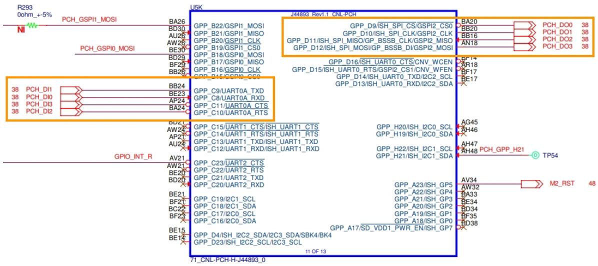
![R293\n0ohm_+5%\nNI\nPCH_GSPI1_MOSI\nBA26\nGPP_B22/GSPI1_MOSI\nGPP_D9/ISH_SPI_CS/GSPI2_CS0\nGPP_D10/ISH_SPI_CLK/GSPI2_CLK\nGPP_D11/ISH_SPI_MISO/GP_BSSB_CLK/GSPI2_MISO\nGPP_D12/ISH_SPI_MOSI/GP_BSSB_DI/GSPI2_MOSI\nPCH_GSPI0_MOSI\nAU26\nGPP_B20/GSPI1_CLK\nGPP_D11/ISH_SPI_MISO/GP_BSSB_CLK/GSPI2_MISO\nGPP_D12/ISH_SPI_MOSI/GP_BSSB_DI/GSPI2_MOSI\nBE30\nGPP_B19/GSPI1_CS0\nGPP_D18/GSPI0_MOSI\nGPP_D16/ISH_UART0_CTS/CNV_WCEN\nGPP_D17/ISH_UART0_RTS/GSPI2_CS1/CNV_WFEN\nGPP_D14/ISH_UART0_TXD/I2C2_SCL\nGPP_D13/ISH_UART0_RXD/I2C2_SDA\nBE29\nGPP_B17/GSPI0_MISO\nGPP_D16/ISH_UART0_CTS/CNV_WCEN\nGPP_D15/ISH_UART0_RTS/GSPI2_CS1/CNV_WFEN\nGPP_D14/ISH_UART0_TXD/I2C2_SCL\nBE23\nGPP_B16/GSPI0_CLK\nGPP_D15/GSPI0_CS0\nGPP_C9/UART0A_TXD\nGPP_C8/UART0A_RXD\nGPP_C11/UART0A_CTS\nGPP_C10/UART0A_RTS\n38 PCH_DI1\nBE24\nGPP_C9/UART0A_TXD\n38 PCH_DI0\nBE23\nGPP_C8/UART0A_RXD\n38 PCH_DI3\nBE24\nGPP_C11/UART0A_CTS\n38 PCH_DI2\nBE24\nGPP_C10/UART0A_RTS\nGPIO_INT_R\nAV21\nGPP_C15/UART1_CTS/ISH_UART1_CTS\nGPP_H20/ISH_I2C0_SCL\nAW22\nGPP_C14/UART1_RTS/ISH_UART1_RTS\nGPP_H19/ISH_I2C0_SDA\nAP23\nGPP_C13/UART1_TXD/ISH_UART1_TXD\nGPP_H22/ISH_I2C1_SCL\nAU24\nGPP_C12/UART1_RXD/ISH_UART1_RXD\nGPP_H21/ISH_I2C1_SDA\nAV21\nGPP_C23/UART2_CTS\nGPP_A23/ISH_GP5\nAW21\nGPP_C22/UART2_RTS\nGPP_A22/ISH_GP4\nBE20\nGPP_C21/UART2_TXD\nGPP_A21/ISH_GP3\nBD20\nGPP_C20/UART2_RXD\nGPP_A20/ISH_GP2\nBE21\nGPP_C19/I2C1_SCL\nGPP_A19/ISH_GP1\nBF21\nGPP_C18/I2C1_SDA\nGPP_A18/ISH_GP0\nBC21\nGPP_C17/I2C0_SCL\nGPP_A17/SD_VDD1_PWR_EN/ISH_GP7\nBE23\nGPP_C16/I2C0_SDA\nGPP_D4/ISH_I2C2_SDA/I2C3_SDA/SBK4/BK4\nBE15\nGPP_D3/ISH_I2C2_SCL/I2C3_SCL\nBE14\nGPP_D4/ISH_I2C2_SDA/I2C3_SDA/SBK4/BK4\n71 CNL-PCH-HJ44893_0](.ava-3510-50m-41051-1040-14/90dd662cc7ea00115cc223bd5b6821d6916205364de38b040710aa3a235e60c8.jpg)

# 2. Check the pinctrl debug system node.

There is a gpiochip device named “INIT3450:00” under the kernel debug system node.

\$ sudo ls -l /sys/kernel/debug/pinctrl
```txt
test@test-AVA-3510:~/Desktop$ sudo ls -l /sys/kernel/debug/pinctrl [sudo] password for test:
total 0
drwxr-xr-x 2 root root 0 Dec 17 14:08 INT3450:00
-r--r--r-- 1 root root 0 Dec 17 14:08 pinctrl-devices
-r--r--r-- 1 root root 0 Dec 17 14:08 pinctrl-handles
-r--r--r-- 1 root root 0 Dec 17 14:08 pinctrl-maps
```

# 3. Check the pinctrl debug functions under the gpiochip device node.

\$ sudo ls -l /sys/kernel/debug/pinctrl/INT3450\:00/
```txt
root@test-AVA-3510:/home/test/Desktop# sudo ls -l /sys/kernel/debug/pinctrl/INT3450\:00/
total 0
-r--r--r-- 1 root root 0 +二 17 14:08 gpio-ranges
-r--r--r-- 1 root root 0 +二 17 14:08 pinconf-groups
-r--r--r-- 1 root root 0 +二 17 14:08 pinconf-pins
-r--r--r-- 1 root root 0 +二 17 14:08 pingroups
-r--r--r-- 1 root root 0 +二 17 14:08 pinmux-functions
-r--r--r-- 1 root root 0 +二 17 14:08 pinmux-pins
--w---- 1 root root 0 +二 17 14:08 pinmux-select
-r--r--r-- 1 root root 0 +二 17 14:08 pins

root@test-AVA-3510:/home/test/Desktop#
```

# 4. Find the “pins function name” under the “pins system node”.

Display function name by pins node

\$ sudo cat /sys/kernel/debug/pinctrl/INT34C6\:00/pins

```tcl
pin 52 (SMBDATA) 65:INT3450:00 mode 1 0x44000402 0x00000049 0x00000000
pin 53 (SMBALERTB) 66:INT3450:00 GPIO 0x44000200 0x0000004a 0x00000000 [ACPI]
pin 54 (SML0CLK) 67:INT3450:00 mode 1 0x44000402 0x0000004b 0x00000000
pin 55 (SML0DATA) 68:INT3450:00 mode 1 0x44000402 0x0000004c 0x00000000
pin 56 (SML0ALERTB) 69:INT3450:00 GPIO 0x44000200 0x0000004d 0x00000000 [ACPI]
pin 57 (SML1CLK) 70:INT3450:00 not available
pin 58 (SML1DATA) 71:INT3450:00 not available
pin 59 (UARTO_RXD) 72:INT3450:00 GPIO 0x82160102 0x0000050 0x0000000
pin 60 (UARTO_TXD) 73:INT3450:00 GPIO 0x82161111 1x666666666666666666666666666666666666666666666666666666666666666666666666666666666666666666
pin 61 (UARTO_RTSB) 74:INT3450:00 GPIO 0x82181111 1x82181111 1x82181111 1x82181111
pin 62 (UARTO_CTSB) 75:INT3450:00 GPIO 0x82181111 1x82181111 1x82181111 1x82181111
pin 63 (UARTI_RXD) 76:INT3450:00 GPIO 0x44003333 1x44443333 1x44443333 1x44443333 1x44443333
pin 64 (UARTI_TXD) 77:INT3450:00 GPIO 0x449999999999999999999999999999999999999999999999999999999
pin 65 (UARTI_RTSB) 78:INT3450:00 GPIO 1x44443333 1x44443333 1x44443333 1x44443333 1x44443333
pin 66 (UARTI_CTSB) 79:INT3450:00 GPIO 1x44443333 1x44443333 1x44443333 1x44443333
pin 67 (I2CQ_SDA) 80:INT345E:GIO mode 1 x444887777777777777777777777777777777777777777
pin 68 (I2CQ_SCL) 81:INT345E:GIO mode 1 x444887777777777777777777777777777777
pin 69 (I2CQ_SDA) 82:INT345E:GIO mode 1 x44488777777777777777777777
pin 70 (I2CQ_SCL) 83:INT345E:GIO mode 1 x44488777777777777777777
pin 71 (UART2_RXD) 84:INT345E:GIO GPIO 1x4448888888888888888888888888888888888888
pin 72 (UART2_TXD) 85:INT345E:GIO GPIO 1x444888888888888888888888888888
pin 73 (UART2_RTSB) 86:INT345E:GIO GPIO 1x444888888888888888888888888
pin 74 (UART2_CTSB) 87:INT345E:GIO GPIO 1x4448888888888888888888888
pin 75 (SPII_CSB) 96:INT345E:GIO GPIO 1x44499999999999999999999999999999999
pin 76 (SPII_CLK) 97:INT345E:GIO GPIO 1x4455555555555555555555555555555555555555555
pin 77 (SPII_MISO_IO_1) 98:INT345E:GIO GPIO 1x44555555555555555555555555
pin 78 (SPII_MOSI_IO_2) 99:INT345E:GIO GPIO 1x445555555555555555555555
pin 79 (ISH_I2C2_SDA) 1.1.INT345E:GIO GPIO 1x4455555555555555555
pin 80 (SSP2_SFRM) 1.2.INT345E:GIO mode 2 x445FfFfF F F F F F F F F F F F F F F F F F F F F F F F F F F F F F F F F F F F F F F F F F F F F F F F F F F F F F F F F F F F F F F F F F F F F F F F F F F F F F F F F F F F F F F F F F F F F F F F F F F F F
```

Refer to the schematics, the DI0/DI1/DI2/DI3 pins are:

PCH\_DI0: GPP\_C8 / UART0A\_RXD
PCH\_DI1: GPP\_C9 / UART0A\_TXD
PCH\_DI2: GPP\_C10 / UART0A\_RTS
PCH\_DI3: GPP\_C11 / UART0A\_CTS
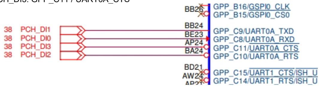
![The diagram, titled **PCH_D15: GPP_G17/GART0A_CTS**, depicts signal routing and pin assignments.\n\n**Left-Side Signals:**\nA group of signals labeled **38 PCH_DI1**, **38 PCH_DI0**, **38 PCH_DI3**, and **38 PCH_DI2** are connected via a red multi-line arrow/bracket to the right side.\n\n**Right-Side Connections (Top Section):**\nThe red bracket routes to a vertical blue bus bar with the following specific pin connections:\n*   **BB26** (marked with an X) connects to **GPP_B16/GSPI0_CLK** and **GPP_B15/GSPI0_CS0**.\n*   **BB24** connects to **GPP_C9/UART0A_TXD**.\n*   **BE23** (marked with an arrow pointing right) connects to **GPP_C8/UART0A_RXD**.\n*   **AP24** connects to **GPP_C11/UART0A_CTS**.\n*   **BA24** connects to **GPP_C10/UART0A_RTS**.\n\n**Bottom Section:**\nAdditional pins connect to the blue bus bar:\n*   **BD21** (marked with an X)\n*   **AW24** (marked with an X)\n*   **AP21** (label partially visible)\n\nThese connect to:\n*   **GPP_C15/UART1_CTS/ISH_U**\n*   **GPP_C14/UART1_RTS/ISH_U**](.ava-3510-50m-41051-1040-14/95e2db6b6ceb04298904dd86463507d578888595e36a582ac13d2a84f5939f60.jpg)

Search the DI pins by function name

\$ sudo cat /sys/kernel/debug/pinctrl/INT34C6\:00/pins | grep -i UART0

```txt
root@test-AVA-3510:/home/test/Desktop# sudo cat /sys/kernel/debug/pinctrl/INT3450\:00/pins | grep -i UART0
pin 59 (UART0_RXD) 72:INT3450:00 GPIO 0x82100100 0x00000050 0x00000000
pin 60 (UART0_TXD) 73:INT3450:00 GPIO 0x82100100 0x00000051 0x00000000
pin 61 (UART0_RTSB) 74:INT3450:00 GPIO 0x82100100 0x00000052 0x00000000
pin 62 (UART0_CTSB) 75:INT3450:00 GPIO 0x82100100 0x00000053 0x00000000
```

DI0/DI1/DI2/DI3 corresponds to pins 59/60/61/62.

Refer to the schematic, the DO0/DO1/DO2/DO3 pins are:

PCH\_DO0: GPP\_D9 / ISH\_SPI\_CS / GSPI2\_CS0
PCH\_DO1: GPP\_D10 / ISH\_SPI\_CLK / GSPI2\_CLK
PCH\_DO2: GPP\_D11 / ISH\_SPI\_MISO / GP\_BSSB\_CLK /GSPI2\_MISO
PCH\_DO3: GPP\_D12 / ISH\_SPI\_MOSI / GP\_BSSB\_DI / GSPI2\_MOSI

![J44893_Rev1.1_CNL-PCH\nGPP_D9/ISH_SPI_CS/GSPI2_CS0\nGPP_D10/ISH_SPI_CLK/GSPI2_CLK\nGPP_D11/ISH_SPI_MISO/GP_BSSB_CLK/GSPI2_MISO\nGPP_D12/ISH_SPI_MOSI/GP_BSSB_DI/GSPI2_MOSI\nBA20\nBB20\nBB16\nAN18\nBF14\nPCH_DO0 38\nPCH_DO1 38\nPCH_DO2 38\nPCH_DO3 38](.ava-3510-50m-41051-1040-14/c00449e16d1478d1efa5068d911dc7b4767fb442f39a4497134854509a1af69a.jpg)

Search the DO pins by function name

\$ sudo cat /sys/kernel/debug/pinctrl/INT34C6\:00/pins | grep -i UART0

![root@test-AVA-3510:/home/test/Desktop# sudo cat /sys/kernel/debug/pinctrl/INT3450\00/pins | grep -i ISH_SPI\npin 84 (ISH_SPI_CSB) 105:INT3450:00 GPIO 0x44000201 0x00000069 0x00000000\npin 85 (ISH_SPI_CLK) 106:INT3450:00 GPIO 0x44000201 0x0000006a 0x00000000\npin 86 (ISH_SPI_MISO) 107:INT3450:00 GPIO 0x44000201 0x0000006b 0x00000000\npin 87 (ISH_SPI_MOSI) 108:INT3450:00 GPIO 0x44000201 0x0000006c 0x00000000](.ava-3510-50m-41051-1040-14/e47a1d2997fec9e096af2fdc5797df1db329b328ecc69c8a9bf8f55470d25eb6.jpg)

DO0/DO1/DO2/DO3 corresponds to pins 84/85/86/87.

# 5. Check the GPIO function number in the schematics.

There are 4 \* DI and 4 \* DO pins
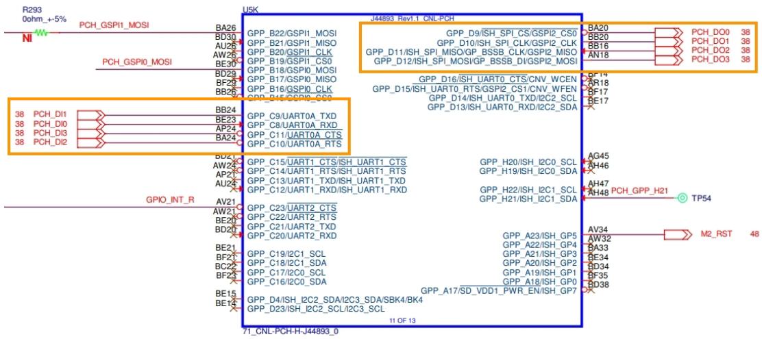
![R293\n0ohm_+5%\nPCH_GSPI1_MOSI\nBA26\nGPP_B22/GSPI1_MOSI\nGPP_D9/ISH_SPI_CS/GSPI2_CS0\nBA20\nPCH_DO0 38\nBD30\nGPP_B21/GSPI1_MISO\nGPP_D10/ISH_SPI_CLK/GSPI2_CLK\nBB20\nPCH_DO1 38\nAU26\nGPP_B20/GSPI1_CLK\nGPP_D11/ISH_SPI_MISO/GP_BSSB_CLK/GSPI2_MISO\nBE16\nPCH_DO2 38\nAW26\nGPP_B19/GSPI1_CS0\nGPP_D12/ISH_SPI_MOSI/GP_BSSB_DIV/GSPI2_MOSI\nBE30\nGPP_B18/GSPI0_MOSI\nGPP_D14/ISH_UART0_CTS/CNV_WCEN\nBP14\nPCH_DO3 38\nPCH_GSPI0_MOSI\nGPP_D15/ISH_UART0_RTS/GSPI2_CS1/CNV_WFEN\nBF15\nPCH_D16/ISH_UART0_TXD/I2C2_SCL\nBP25\nGPP_C9/UART0A_TXD\nGPP_D14/ISH_UART0_RXD/I2C2_SDA\nBP24\nGPP_C8/UART0A_RXD\nGPP_D13/ISH_UART0_RXD/I2C2_SDA\nBP23\nGPP_C7/UART0A_CTS\nGPP_D12/UART0A_RTX\nGPP_D11/UART0A_RTX\nGPP_C10/UART0A_RTXS\nGPP_C9/UART0A_TXD\nGPP_D10/UART0A_CTS\nGPP_D8/UART0A_RXD\nGPP_D7/UART0A_TXD/I2C2_SCL\nGPP_D6/UART0A_CTS\nGPP_D5/UART0A_TXD/I2C2_SCL\nGPP_D4/UART0A_CTS\nGPP_D3/UART0A_TXD/I2C2_SCL\nGPP_D2/UART0A_CTS\nGPP_D1/UART0A_TXD/I2C2_SCL\nGPP_D9/UART0A_TXD/I2C2_SCL\nGPP_D7/UART0A_TXD/I2C2_SCL\nGPP_D6/UART0A_TXD/I2C2_SCL\nGPP_D5/UART0A_TXD/I2C2_SCL\nGPP_D4/UART0A_TXD/I2C2_SCL\nGPP_D3/UART0A_TXD/I2C2_SCL\nGPP_D2/UART0A_TXD/I2C2_SCL\nGPP_D1/UART0A_TXD/I2C2_SCL\nGPP_D9/UART0A_TXD/I2C2_SCL\nGPP_D7/UART0A_TXD/I2C2_SCL\nGPP_D6/UART0A_TXD/I2C2_SCL\nGPP_D5/UART0A_TXD/I2C2_SCL\nGPP_D4/UART0A_TXD/I2C2_SCL\nGPP_EUT_R\nGPIO_INT_R\nAV21\nGPP_C15/UART1_CTS/ISH_UART1_CTS\nGPP_H20/ISH_I2C0_SCL\nAV24\nGPP_C14/UART1_RTS/ISH_UART1_RTS\nGPP_H19/ISH_I2C0_SDA\nAV23\nGPP_C13/UART1_TXD/ISH_UART1_TXD\nGPP_H22/ISH_I2C1_SCL\nAV25\nGPP_C12/UART1_RXD/ISH_UART1_RXD\nGPP_H21/ISH_I2C1_SDA\nAV26\nGPP_C15/UART1_CTS/ISH_UART1_CTS\nGPP_H19/ISH_I2C0_SDA\nAV27\nGPP_C14/UART1_RTS/ISH_UART1_RTS\nGPP_H22/ISH_I2C1_SCL\nAV28\nGPP_C13/UART1_TXD/ISH_UART1_TXD\nGPP_H21/ISH_I2C1_SDA\nAV29\nGPP_C12/UART1_RXD/ISH_UART1_RXD\nGPP_H24/\nGPP_C9/UART0A_TXD/I2C2_SCL\nAV30\nGPP_C8/UART0A_RXD/I2C2_SCL\nAV31\nGPP_C7/UART0A_TXD/I2C2_SCL\nAV32\nGPP_C6/UART0A_TXD/I2C2_SCL\nAV33\nGPP_C5/UART0A_TXD/I2C2_SCL\nAV34\nGPP_C4/UART0A_TXD/I2C2_SCL\nAV35\nGPP_C3/UART0A_TXD/I2C2_SCL\nAV36\nGPP_C2/UART0A_TXD/I2C2_SCL\nAV37\nGPP_C1/UART0A_TXD/I2C2_SCL\nAV38\nGPP_C0/UART0A_TXD/I2C2_SCL\nAV39\nGPP_C9/UART0A_TXD/I2C2_SCL\nAV40\nGPP_C8/UART0A_TXD/I2C2_SCL\nAV41\nGPP_C7/UART0A_TXD/I2C2_SCL\nAV42\nGPP_C6/UART0A_TXD/I2C2_SCL\nAV43\nGPP_C5/UART0A_TXD/I2C2_SCL\nAV44\nGPP_C4/UART0A_TXD/I2C2_SCL\nAV45\nGPP_C3/UART0A_TXD/I2C2_SCL\nAV46\nGPP_C2/UART0A_TXD/I2C2_SCL\nAV47\nGPP_C1/UART0A_TXD/I2C2_SCL\nAV48\nGPP_C0/UART0A_TXD/I2C2_SCL\nAV49\nGPP_C9/UART0A_TXD/I2C2_SCL\nAV50\nGPP_C8/UART0A_TXD/I2C2_SCL\nAV51\nGPP_C7/UART0A_TXD/I2C2_SCL\nAV52\nGPP_C6/UART0A_TXD/I2C2_SCL\nAV53\nGPP_C5/UART0A_TXD/I2C2_SCL\nAV54\nGPP_C4/UART0A_TXD/I2C2_SCL\nAV55\nGPP_C3/UART0A_TXD/I2C2_SCL\nAV56\nGPP_C2/UART0A_TXD/I2C2_SCL\nAV57\nGPP_C1/UART0A_TXD/I2C2_SCL\nAV58\nGPP_C0/UART0A_TXD/I2C2_SCL\nAV59\nGPP_C9/UART0A_TXD/I2C2_SCL\nAV60\nGPP_C8/UART0A_TXD/I2C2_SCL\nAV61\nGPP_C7/UART0A_TXD/I2C2_SCL\nAV62\nGPP_C6/UART0A_TXD/I2C2_SCL\nAV63\nGPP_C5/UART0A_TXD/I2C2_SCL\nAV64\nGPP_C4/UART0A_TXD/I2C2_SCL](.ava-3510-50m-41051-1040-14/1d1b6d40918866eda56e607149ebea074befa4a77430cf4f20bcea9869e46a98.jpg)

# 6. Check the pinctrl debug system node.

There is a gpiochip device named “INIT3450:00” under the kernel debug system node.

\$ sudo ls -l /sys/kernel/debug/pinctrl
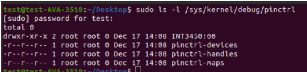
![test@test-AVA-3510:~/Desktop\$ sudo ls -l /sys/kernel/debug/pinctrl\n(sudo) password for test:\ntotal 0\ndrwxr-xr-x 2 root root 0 Dec 17 14:08 INT3450:00\n-r--r--r-- 1 root root 0 Dec 17 14:08 pinctrl-devices\n-r--r--r-- 1 root root 0 Dec 17 14:08 pinctrl-handles\n-r--r--r-- 1 root root 0 Dec 17 14:08 pinctrl-maps\ntest@test-AVA-3510:~/Desktop\$](.ava-3510-50m-41051-1040-14/dc4fe715533c1756eb56fadc557433f52139138de17c10898ca623750f0bbdf7.jpg)

# 7. Check the pinctrl debug functions under the gpiochip device node

\$ sudo ls -l /sys/kernel/debug/pinctrl/INT3450\:00/

```txt
root@test-AVA-3510:/home/test/Desktop# sudo ls -l /sys/kernel/debug/pinctrl/INT3450\:00/
total 0
-r--r--r-- 1 root root 0 +二 17 14:08 gpio-ranges
-r--r--r-- 1 root root 0 +二 17 14:08 pinconf-groups
-r--r--r-- 1 root root 0 +二 17 14:08 pinconf-pins
-r--r--r-- 1 root root 0 +二 17 14:08 pingroups
-r--r--r-- 1 root root 0 +二 17 14:08 pinmux-functions
-r--r--r-- 1 root root 0 +二 17 14:08 pinmux-pins
--w---- 1 root root 0 +二 17 14:08 pinmux-select
-r--r--r-- 1 root root 0 +二 17 14:08 pins
root@test-AVA-3510:/home/test/Desktop#
```

# 8. Find the “pins function name” under the “pins system node”

Display the function name by the pins node

\$ sudo cat /sys/kernel/debug/pinctrl/INT34C6\:00/pins

```tcl
pin 52 (SMBDATA) 65:INT3450:00 mode 1 0x44000402 0x00000049 0x00000000
pin 53 (SMBALERTB) 66:INT3450:00 GPIO 0x44000200 0x0000004a 0x00000800 [ACPI]
pin 54 (SML0CLK) 67:INT3450:00 mode 1 0x44000402 0x0000004b 0x00000000
pin 55 (SML0DATA) 68:INT3450:00 mode 1 0x44000402 0x0000004c 0x00000000
pin 56 (SML0ALERTB) 69:INT3450:00 GPIO 0x44000200 0x0000004d 0x00000000 [ACPI]
pin 57 (SML1CLK) 70:INT3450:00 not available
pin 58 (SML1DATA) 71:INT3450:00 not available
pin 59 (UARTO_RXD) 72:INT3450:00 GPIO 0x82100102 0x0000050 0x00000000
pin 60 (UARTO_TXD) 73:INT3450:00 GPIO 0x82100100 0x0000051 0x00000000
pin 61 (UARTO_RTSB) 74:INT3450:00 GPIO 0x82100100 0x0000052 0x00000000
pin 62 (UARTO_CTSB) 75:INT3450:00 GPIO 0x82100102 0x0000053 0x00000000
pin 63 (UARTI_RXD) 76:INT3450:00 GPIO 0x4400338 1x34555555555555555555555555555555555555555555555555555
pin 64 (UARTI_TXD) 77:INT3458:38
pin 65 (UARTI_RTSB) 78:INT3458:38
pin 66 (UARTI_CTSB) 79:INT3458:38
pin 67 (I2COSDA) 81:INT3458:38
pin 68 (I2COSCL) 82:INT3458:38
pin 69 (I2C1_SDA) 83:INT3458:38
pin 71 (UART2_RXD) 84:INT3458:38
pin 72 (UART2_TXD) 85:INT3458:38
pin 73 (UART2_RTSB) 86:INT3458:38
pin 74 (UART2_CTSB) 87:INT3458:38
pin 75 (SPI1_CSB) 96:INT3458:38
pin 76 (SPI1_CLK) 97:INT3458:38
pin 77 (SPI1_MISO_IO_1) 98:INT3458:38
pin 78 (SPI1_MOSI_IO_1) 99:INT3458:38
pin 79 (ISH_I2C2_SDA) 1.1.INT3458:38
pin 81 (SSP2_SFRM) 1.1.INT3458:38
pin 82 (SSP2_TXD) 1.2.INT3458:38
pin 83 (SSP2_RXD) 1.2.INT3458:38
pin 84 (ISH_SPI_CSB) 1.2.INT3458:38
pin 85 (ISH_SPI_CLK) 1.2.INT3458:38
pin 86 (ISH_SPI_MISO) 1.2.INT3458:38
pin 87 (ISH_SPI_MOSI) 1.2.INT3458:38
pin 88 (ISH_UARTO_RXD) 1.2.INT3458:38
pin 89 (ISH_UARTO_TXD) 1.2.INT3458:38
pin 91 (ISH_UARTO_RTSB) 1.2.INT3458:38
pin 92 (ISH_UARTO_CTSB) 1.2.INT3458:38
```

Refer to the schematics, the DI0/DI1/DI2/DI3 pins are:

. PCH\_DI0: GPP\_C8 / UART0A\_RXD
PCH\_DI1: GPP\_C9 / UART0A\_TXD
PCH\_DI2: GPP\_C10 / UART0A\_RTS
PCH\_DI3: GPP\_C11 / UART0A\_CTS
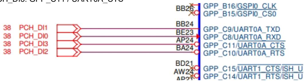
![The diagram displays a connection mapping between a set of input signals on the left and pin labels on the right.\n\n**Labeled Blocks:**\n\n*   **Left Side:**\n    *   38 PCH_DI1\n    *   38 PCH_DI0\n    *   38 PCH_DI3\n    *   38 PCH_DI2\n*   **Right Side (Top to Bottom):**\n    *   BB26\n    *   GPP_B16/GSPI0_CLK\n    *   GPP_B15/GSPI0_CS0\n    *   BB24\n    *   BE23\n    *   GPP_C9/UART0_TXD\n    *   AP24\n    *   GPP_C8/UART0_RXD\n    *   BA24\n    *   GPP_C11/UART0_CTS\n    *   BD21\n    *   GPP_C10/UART0_RTS\n    *   AW24\n    *   GPP_C15/UART1_CTS/ISH_U\n    *   AP21 (partially visible)\n    *   GPP_C14/UART1_RTS/ISH_U\n\n**Connections:**\n\n*   **38 PCH_DI1** connects to **BE23** (associated with GPP_C9/UART0_TXD)\n*   **38 PCH_DI0** connects to **AP24** (associated with GPP_C8/UART0_RXD)\n*   **38 PCH_DI3** connects to **BA24** (associated with GPP_C11/UART0_CTS)\n*   **38 PCH_DI2** connects to **BD21** (associated with GPP_C10/UART0_RTS)](.ava-3510-50m-41051-1040-14/7244259a1ef31b9d9593655ef11ad40e001e5f0dc7b15cf6819af5c2cbe2ccc7.jpg)

# Search the DI pins by function name

\$ sudo cat /sys/kernel/debug/pinctrl/INT34C6\:00/pins | grep -i UART0

```txt
root@test-AVA-3510:/home/test/Desktop# sudo cat /sys/kernel/debug/pinctrl/INT3450\:00/pins | grep -i UART0
pin 59 (UART0_RXD) 72:INT3450:00 GPIO 0x82100100 0x00000050 0x00000000
pin 60 (UART0_TXD) 73:INT3450:00 GPIO 0x82100100 0x00000051 0x00000000
pin 61 (UART0_RTSB) 74:INT3450:00 GPIO 0x82100100 0x00000052 0x00000000
pin 62 (UART0_CTSB) 75:INT3450:00 GPIO 0x82100100 0x00000053 0x00000000
```

DI0/DI1/DI2/DI3 corresponds to pins 59/60/61/62.

Refer to the schematic, the DO0/DO1/DO2/DO3 pins are:

 PCH\_DO0: GPP\_D9 / ISH\_SPI\_CS / GSPI2\_CS0
 PCH\_DO1: GPP\_D10 / ISH\_SPI\_CLK / GSPI2\_CLK
PCH\_DO2: GPP\_D11 / ISH\_SPI\_MISO / GP\_BSSB\_CLK /GSPI2\_MISO
PCH\_DO3: GPP\_D12 / ISH\_SPI\_MOSI / GP\_BSSB\_DI / GSPI2\_MOSI

![J44893_Rev1.1_CNL-PCH\nGPP_D9/ISH_SPI_CS/GSPI2_CS0\nGPP_D10/ISH_SPI_CLK/GSPI2_CLK\nGPP_D11/ISH_SPI_MISO/GP_BSSB_CLK/GSPI2_MISO\nGPP_D12/ISH_SPI_MOSI/GP_BSSB_DI/GSPI2_MOSI\nBA20\nBB20\nBB16\nAN18\nBF14\nPCH_DO0 38\nPCH_DO1 38\nPCH_DO2 38\nPCH_DO3 38](.ava-3510-50m-41051-1040-14/e572bfc0501fb6636710a2dd6977532f2c7b3de22a3cbb8c0a53acb698896cfa.jpg)

# Search the DO pins by function name

\$ sudo cat /sys/kernel/debug/pinctrl/INT34C6\:00/pins | grep -i UART0

```txt
root@test-AVA-3510:/home/test/Desktop# sudo cat /sys/kernel/debug/pinctrl/INT3450:\00/pins | grep -i ISH_SPI
pin 84 (ISH_SPI_CSB) 105:INT3450:00 GPIO 0x44000201 0x00000069 0x00000000
pin 85 (ISH_SPI_CLK) 106:INT3450:00 GPIO 0x44000201 0x0000006a 0x00000000
pin 86 (ISH_SPI_MISO) 107:INT3450:00 GPIO 0x44000201 0x0000006b 0x00000000
pin 87 (ISH_SPI_MOSI) 108:INT3450:00 GPIO 0x44000201 0x0000006c 0x00000000
```

DO0/DO1/DO2/DO3 corresponds to pins 84/85/86/87.

# 9. Find the Pins’ function group under gpio-ranges system node

Pins 97 & 98 in PINS group [79 - 104], GPIOS number range is [689 – 714]

\$ sudo cat /sys/kernel/debug/pinctrl/INT3450\:00/gpio-ranges

```txt
root@test-AVA-3510:/home/test/Desktop# sudo cat /sys/kernel/debug/pinctrl/INT3450\:00/gpio-ranges
GPIO ranges handled:
0: INT3450:00 GPIOS [660 - 684] PINS [0 - 24]
32: INT3450:00 GPIOS [692 - 717] PINS [25 - 50]
64: INT3450:00 GPIOS [724 - 747] PINS [51 - 74]
96: INT3450:00 GPIOS [756 - 779] PINS [75 - 98]
128: INT3450:00 GPIOS [788 - 795] PINS [99 - 106]
160: INT3450:00 GPIOS [820 - 851] PINS [115 - 146]
192: INT3450:00 GPIOS [852 - 875] PINS [155 - 178]
224: INT3450:00 GPIOS [884 - 907] PINS [179 - 202]
256: INT3450:00 GPIOS [916 - 928] PINS [203 - 215]
288: INT3450:00 GPIOS [948 - 971] PINS [216 - 239]
320: INT3450:00 GPIOS [980 - 997] PINS [269 - 286]
352: INT3450:00 GPIOS [1012 - 1023] PINS [287 - 298]
root@test-AVA-3510:/home/test/Desktop#
```

The DI pins 59/60/61/62 in PINS group [51 - 74], GPIOs range [724 – 747]

The DO pins 84/85/86/87 in PINS group [75 - 98], GPIOs range [756 – 779]

Calculate DI pins using GPIO number: 732/733/734/735 on this Linux kernel

$$
\mathrm{DI0} = \text { pin59 } = \text { gpio732(59 - 51 + 724 = 732)}
$$

$$
\mathrm{DI} 1 = \text { pin60 } = \text { gpio733(60 - 51 + 724 = 733)}
$$

$$
\mathrm{DI2} = \text { pin61 } = \text { gpio734(61 - 51 + 724 = 734)}
$$

$$
\mathrm{DI3} = \text { pin62 } = \text { gpio735(62 - 51 + 724 = 735)}
$$

Calculate DO pins using GPIO number: 765/766/767/768 on this Linux kernel

$$
\mathrm{DO0} = \text { pin84 } = \text { gpio765(84 - 75 + 756 = 765)}
$$

$$
\mathrm{DO1} = \text { pin85 } = \text { gpio766(85 - 51 + 756 = 766)}
$$

$$
\mathrm{DO2} = \text { pin86 } = \text { gpio767(86 - 51 + 756 = 767)}
$$

$$
\mathrm{DO3} = \text { pin87 } = \text { gpio768(87 - 51 + 756 = 768)}
$$

# 7.4 Test the GPIO Function

DIO control from PCH GPIO: Pin is gpio 732\~735 and gpio 765\~768 are used for this platform.

# 1. Add the corresponding GPIO number to the system node. The DIO is controlled by PCH GPIO

```shell
sudo echo 732 > /sys/class/gpio/export
sudo echo 733 > /sys/class/gpio/export
sudo echo 734 > /sys/class/gpio/export
sudo echo 735 > /sys/class/gpio/export
sudo echo 765 > /sys/class/gpio/export
sudo echo 766 > /sys/class/gpio/export
sudo echo 767 > /sys/class/gpio/export
sudo echo 768 > /sys/class/gpio/export
```

# 2. The DI direction is the input, the DO direction is the output

```shell
sudo echo in > /sys/class/gpio/gpio732/direction
sudo echo in > /sys/class/gpio/gpio733/direction
sudo echo in > /sys/class/gpio/gpio734/direction
sudo echo in > /sys/class/gpio/gpio735/direction
sudo echo out > /sys/class/gpio/gpio765/direction
sudo echo out > /sys/class/gpio/gpio766/direction
sudo echo out > /sys/class/gpio/gpio767/direction
sudo echo out > /sys/class/gpio/gpio768/direction
```

# 3. Check the DIO gpio state.

\$ cat /sys/kernel/debug/gpio
```txt
test@test-AVA-3510:~/AVA-3510/utility/DIO_Test$ sudo cat /sys/kernel/debug/gpio
gpiochip2: GPIOs 655-657, parent: usb/1-6:1.1, cp210x, can sleep:
gpiochip1: GPIOs 658-659, parent: usb/1-6:1.0, cp210x, can sleep:
gpiochip0: GPIOs 660-1023, parent: platform/INT3450:00, INT3450:00:
gpio-732 (    |sysfs    ) in lo
gpio-733 (    |sysfs    ) in lo
gpio-734 (    |sysfs    ) in lo
gpio-735 (    |sysfs    ) in lo
gpio-765 (    |sysfs    ) out lo
gpio-766 (    |sysfs    ) out lo
gpio-767 (    |sysfs    ) out lo
gpio-768 (    |sysfs    ) out lo
```

# 4. Get DI GPIO value.

```shell
$ sudo cat /sys/class/gpio/gpio732/value
$ sudo cat /sys/class/gpio/gpio733/value
$ sudo cat /sys/class/gpio/gpio734/value
$ sudo cat /sys/class/gpio/gpio735/value
```

# 5. Set the DO GPIO value "1" to output high.

```shell
$ sudo echo 1 > /sys/class/gpio/gpio765/value
$ sudo echo 1 > /sys/class/gpio/gpio766/value
$ sudo echo 1 > /sys/class/gpio/gpio767/value
$ sudo echo 1 > /sys/class/gpio/gpio768/value
```

# 6. Set the DO GPIO value "0" to output low.

```shell
$ sudo echo 0 > /sys/class/gpio/gpio765/value
$ sudo echo 0 > /sys/class/gpio/gpio766/value
$ sudo echo 0 > /sys/class/gpio/gpio767/value
$ sudo echo 0 > /sys/class/gpio/gpio768/value
```

# 7. Remove the DIO GPIO used, unregister the corresponding GPIO number to the system node.

```shell
sudo echo 732 > /sys/class/gpio/unexport
sudo echo 733 > /sys/class/gpio/unexport
sudo echo 734 > /sys/class/gpio/unexport
sudo echo 735 > /sys/class/gpio/unexport
sudo echo 765 > /sys/class/gpio/unexport
sudo echo 766 > /sys/class/gpio/unexport
sudo echo 767 > /sys/class/gpio/unexport
sudo echo 768 > /sys/class/gpio/unexport
```

# Safety Instructions

Read and follow all instructions marked on the product and in the documentation before you operate your system. Retain all safety and operating instructions for future use.

Please read these safety instructions carefully.
• Please keep this User‘s Manual for later reference.
• Read the specifications section of this manual for detailed information on the operating environment of this equipment.
• When installing/mounting or uninstalling/removing equipment, turn off the power and unplug any power cords/cables.
• To avoid electrical shock and/or damage to equipment:

Keep equipment away from water or liquid sources.
Keep equipment away from high heat or high humidity.
 Keep equipment properly ventilated (do not block or cover ventilation openings).
 Make sure to use recommended voltage and power source settings.
Secure the power cord (do not place any object on/over the power cord).
 Only install/attach and operate equipment on stable surfaces and/or recommended mountings.
 If the equipment will not be used for long periods of time, turn off and unplug the equipment from its power source.

• Never attempt to fix the equipment. Equipment should only be serviced by qualified personnel.

# Getting Services

Ask an Expert: https://www.adlinktech.com/en/Askanexpert

# ADLINK Technology, Inc.

Address: No. 66, Huaya 1st Road, Guishan District Taoyuan City 333, Taiwan

Tel: +886-3-216-5088

Fax: +886-3-328-5723

Email: service@adlinktech.com

# Ampro ADLINK Technology, Inc.

Address: 6450 Via Del Oro, San Jose, CA 95119-1208, USA

Tel: +1-408-360-0200

Toll Free: +1-800-966-5200 (USA only)

Fax: +1-408-600-1189

Email: info@adlinktech.com

# ADLINK Technology (China) Co., Ltd.

Address: 300 Fang Chun Rd., Zhangjiang Hi-Tech Park, Pudong New Area Shanghai, 201203 China

Tel: +86-21-5132-8988

Fax: +86-21-5132-3588

Email: market@adlinktech.com

# ADLINK Technology GmbH

Address: Hans-Thoma-Strasse 8-10, 68163 Mannheim, Germany

Tel: +49-621-43214-0

Fax: +49-621 43214-30

Email: emea@adlinktech.com

Please visit the Contact page at https://www.adlinktech.com for information on how to contact the ADLINK regional office nearest you.
[🔗 Link to the original document](.ava-3510-50m-41051-1040-14/ava-3510-50m-41051-1040-14.pdf)
