# CM1-86DX3

# Technical Reference

PC/104 Single Board Computer with Vortex86-DX3 SoC

![Green printed circuit board with various electronic components and connectors (no readable text or symbols)](.cm1-86dx3-50m-00084-1060-25/74b3e6086885be9f2e65df85127e273290025df847e1d7fc4bc6444af9cad33e.jpg)

Manual Rev.: 2.5

Revision Date: July 12, 2022

Part Number: 50M-00084-1060

# Preface

# Disclaimer

Information in this document is provided in connection with ADLINK products. No license, express or implied, by estoppel or otherwise, to any intellectual property rights is granted by this document. Except as provided in ADLINK´s Terms and Conditions of Sale for such products, ADLINK assumes no liability whatsoever, and ADLINK disclaims any express or implied warranty, relating to sale and/or use of ADLINK products including liability or warranties relating to fitness for a particular purpose, merchantability, or infringement of any patent, copyright or other intellectual property right. If you intend to use ADLINK products in or as medical devices, you are solely responsible for all required regulatory compliance, including, without limitation, Title 21 of the CFR (US), Directive 2007/47/EC (EU), and ISO 13485 & 14971, if any. ADLINK may make changes to specifications and product descriptions at any time, without notice.

# Trademarks

Product names mentioned herein are used for identification purposes only and may be trademarks and/or registered trademarks of their respective companies.

Revision History

<table><tr><td>Revision</td><td>Reason for Change</td><td>Date</td></tr><tr><td>1.00</td><td>Initial Release</td><td>Oct/15</td></tr><tr><td>2.00</td><td>Added VGA DDC interface to Chapter 3; revised CFast information; added CFast pinout Chapter 3; transposed CN14 and CN16 headers for COM1 and COM2; added cooling airflow specifications; added Getting Started section to chapter 1; added Component Features section to chapter 2; restructured the format of this manual to four chapters</td><td>Jul/16</td></tr><tr><td>2.1</td><td>Added Appendix B, System Resources; updated Ordering Information in Table 1-1</td><td>Jan/18</td></tr><tr><td>2.2</td><td>Revised RS485/422 mode signals in Table 3-1; changed positions of labels for jumper headers in Figure 2-5; added Prop 65 warning and Battery labels to Preface</td><td>Jul/18</td></tr><tr><td>2.3</td><td>Removed SPI flash support; add heat sink installation</td><td>2020-04-24</td></tr><tr><td>2.4</td><td>Add French safety warnings</td><td>2021-02-04</td></tr><tr><td>2.5</td><td>Update specifications</td><td>2022-07-12</td></tr></table>

Copyright © 2015, 2016, 2017, 2018, 2020, 2021, 2022 ADLINK Technology, Inc.

This document contains proprietary information protected by copyright. All rights are reserved. No part of this manual may be reproduced by any mechanical, electronic, or other means in any form without prior written permission of the manufacturer.

# Audience

This manual provides reference only for computer design engineers, including but not limited to hardware and software designers and applications engineers. ADLINK Technology, Inc. assumes you are qualified to design and implement prototype computer equipment.

# Environmental Responsibility

ADLINK is committed to fulfill its social responsibility to global environmental preservation through compliance with the European Union's Restriction of Hazardous Substances (RoHS) directive and Waste Electrical and Electronic Equipment (WEEE) directive. Environmental protection is a top priority for ADLINK. We have enforced measures to ensure that our products, manufacturing processes, components, and raw materials have as little impact on the environment as possible. When products are at their end of life, our customers are encouraged to dispose of them in accordance with the product disposal and/or recovery programs prescribed by their nation or company.

![Symbol of a trash bin crossed with a diagonal line and a horizontal bar below (no text or labels)](.cm1-86dx3-50m-00084-1060-25/845b105b6066f5940297226541e96d27cfcd81980a374ce302e290c5df505035.jpg)

Battery Labels (for products with battery)

![Symbol of a trash bin crossed out by two diagonal lines (no text or numbers present)](.cm1-86dx3-50m-00084-1060-25/97a84f854877887bc173919633c01db2cad64d5511236ff74e077cef97f7797e.jpg)

![The image displays a black outline of the standard recycling symbol (three arrows chasing each other in a triangular loop) centered within a square border. Below the square, the text '**Li-ion**' is written in a bold, black, sans-serif font.](.cm1-86dx3-50m-00084-1060-25/09fbd070e644d56dcd3d8ee109616658f7528a88ebf370016fb268181bc8ad9b.jpg)

![RECYCLE\nRBRC\nLi-ion\n7.800.822.8837](.cm1-86dx3-50m-00084-1060-25/2eb7fe0611427446cec64540a86516e18aa793c4adc8270b24567ff0b22a4579.jpg)

![The image displays a black and white graphic containing a recycling symbol and text. The symbol is a black shape resembling a square with rounded corners, featuring four white arrows pointing outwards in the four cardinal directions (up, down, left, right) arranged in a circular pattern. Below the symbol is black text in Traditional Chinese characters: '廢電池請回收'. This text translates to 'Waste batteries, please recycle'.](.cm1-86dx3-50m-00084-1060-25/16e301f336a83d0ec5a549d63bffcfe7ed7cf64334d262e02a911794af15b043.jpg)

# California Proposition 65 Warning

WARNING: This product can expose you to chemicals including acrylamide, arsenic, benzene, cadmium, Tris(1,3-dichloro-2-propyl)phosphate (TDCPP), 1,4-Dioxane, formaldehyde, lead, DEHP, styrene, DINP, BBP, PVC, and vinyl materials, which are known to the State of California to cause cancer, and acrylamide, benzene, cadmium, lead, mercury, phthalates, toluene, DEHP, DIDP, DnHP, DBP, BBP, PVC, and vinyl materials, which are known to the State of California to cause birth defects or other reproductive harm. For more information go to www.P65Warnings.ca.gov.

AVERTISSEMENT: Ce produit peut vous exposer à des produits chimiques tels que l'acrylamide, l'arsenic, le benzène, le cadmium, le phosphate de tris (1,3-dichloro-2-propyle) (TDCPP), le 1,4-dioxane, le formaldéhyde, le plomb, le DEHP, le styrène, le DINP , BBP, PVC et matériaux en vinyle, qui sont connus dans l'État de Californie pour causer le cancer, et acrylamide, benzène, cadmium, plomb, mercure, phtalates, toluène, DEHP, DIDP, DnHP, DBP, BBP, PVC et vinyle matériaux, qui sont connus de l'État de Californie pour causer des anomalies congénitales ou d'autres troubles de la reproduction. Pour plus d'informations, visitez le site www.P65Warnings.ca.gov.

# Conventions

The following conventions may be used throughout this manual, denoting special levels of information.

![The image displays a digital icon of a white document with a folded top-right corner. A large, red checkmark is centered on the page.](.cm1-86dx3-50m-00084-1060-25/4c33b9d9bc65ddd161a0c23f11f6e9c38d3f8bf9cdcc348db858d40ddfe3df3b.jpg)
NOTE:

This information adds clarity or specifics to text and illustrations.

![A yellow triangular warning sign with a black border featuring a black exclamation mark in the center.](.cm1-86dx3-50m-00084-1060-25/50f682074e6e9e2234f16b3d3d3a498c46327a2f9bc2d6902ec3acc4f31f6af9.jpg)
CAUTION:

MISE EN GARDE

This information indicates the possibility of minor physical injury, component damage, data loss, and/or program corruption.

Ces informations indiquent la possibilité de blessures physiques mineures, de dommages aux composants, de perte de données et / ou de corruption de programme.

![The image displays a red triangular warning sign with a white border. Inside the triangle is a large white exclamation point centered vertically and horizontally. The background surrounding the triangle is white.](.cm1-86dx3-50m-00084-1060-25/bef43047728b2203bb77fabe040ebd75902e1e24e9802392f9889b9df836ac12.jpg)
WARNING:

ATTENTION

This information warns of possible serious physical injury, component damage, data loss, and/or program corruption.

Ces informations mettent en garde contre d'éventuelles blessures physiques graves, des dommages aux composants, une perte de données et / ou une corruption du programme.

# Important Safety Instructions

For user safety, please read and follow all Instructions, WARNINGs, CAUTIONs, and NOTEs marked in this manual and on the associated equipment before handling/operating the equipment.

 Read these safety instructions carefully.
 Keep this manual for future reference.
 Read the specifications section of this manual for detailed information on the operating environment of this equipment.
 Turn off power and unplug any power cords/cables when installing/mounting or un-installing/removing equipment.

 To avoid electrical shock and/or damage to equipment:

 Keep equipment away from water or liquid sources;
 Keep equipment away from high heat or high humidity;
 Keep equipment properly ventilated (do not block or cover ventilation openings);
 Make sure to use recommended voltage and power source settings;
 Always install and operate equipment near an easily accessible electrical socketoutlet;
 Secure the power cord (do not place any object on/over the power cord);
 Only install/attach and operate equipment on stable surfaces and/or recommended mountings; and,

If the equipment will not be used for long periods of time, turn off the power source and unplug the equipment.

# Table of Contents

# Preface ... ii

# 1 Product Overview.........

1.1 Description..
1.2 About this Manual ..
1.3 Features... .2
1.4 Ordering Information .... .2
1.5 Block Diagram .. 3
1.6 Specifications.... .4

1.6.1 Physical .4
1.6.2 Mechanical . 4
1.6.3 Electrical . .5
1.6.4 Power .... .5
1.6.5 Environmental . . 5
1.6.6 Thermal/Cooling Requirements.... .6

1.7 Heat Sink Installation .. .. 8
1.8 Getting Started.. .. 11

# 2 Hardware ............ ..... 13

2.1 Major IC Definitions and Locations ... . 13
2.2 Header, Connector, and Socket Definitions.. .. 16
2.3 Jumper Header Definitions .... .. 19
2.4 Component Features .... . 20

2.4.1 CPU .. .. 20
2.4.2 SDRAM .20
2.4.3 LAN Controller ... .. 20
2.4.4 CFast Card Slot .. .. 21

# 3 Interfaces .. 2 3

3.1 Serial Interfaces ..... . 23
3.2 USB Interfaces.... .26
3.3 Utility Interface .... .26

3.3.1 Keyboard . .. 26
3.3.2 Mouse... .. 26
3.3.3 Battery ... .. 26
3.3.4 Reset Switch.. .. 27
3.3.5 Speaker ... . 27

3.4 Fast Ethernet Interface .27
3.5 Gigabit Ethernet Interface . 28
3.6 Gigabit Ethernet External LED Interface.... . 28
3.7 Video (TFT/VGA) Interface .... . 28
3.8 VGA DDC (Display Data Channel) .. . 30
3.9 Power Interface ..... ..30
3.10 Battery Interface . .30

3.11 Power Button Interface.. . 31
3.12 CFast Mass Storage Socket.. .. 31

# 4 Utilities ... . 33

4.1 BIOS Setup ... . 33

4.1.1 Configuring the BIOS .. . 33
4.1.2 Main screen of the BIOS .. . 33
4.1.3 Advanced Settings screen ... . 34
4.1.4 Boot screen .. . 37
4.1.5 Security screen . . 38
4.1.6 Exit screen .. . 39

4.2 SEMA Functions . . 40

4.2.1 Board Specific SEMA functions . . 41

4.3 Real Time Clock (RTC) 42
4.4 User GPIO Interface.. . 43
4.5 Oops! Jumper (BIOS Recovery).. . 43
4.6 Serial Console .... 43
4.7 Serial Console BIOS Setup ....... 43
4.8 Hot (Serial) Cable 44
4.9 Watchdog Timer ....... 44

# Appendix A System Resources..... ..... 45

4.10 Memory Address Map .. . 45
4.11 I/O Address Map . . 47
4.12 PCI Configuration Registers..... 49
4.13 IO Register Maps .... . 50

4.13.1 CMOS Memory and RTC Registers... . 50

4.14 Interrupts .. . 51
4.14.1 SERIRQ Interrupt Mapping . . 51

# Appendix B Technical Support . 53

# 1 Product Overview

# 1.1 Description

The CM1-86DX3 is a PC/104 Single Board Computer (SBC) based on DMP’s Vortex86-DX3 single chip solution, featuring exceptionally high integration and an optimum performance-to-power ratio. The board supports all peripherals needed for an embedded PC on a small 3.55" by 3.77" printed circuit board.

The Vortex86-DX3 chip integrates a powerful yet efficient CPU with graphics, memory, and I/O controller hubs to form a complete PC, with all the standard peripheral connections onboard.

The board provides two Ethernet ports (1x Gbps and 1x 100Mbps), two RS232 serial ports, two RS232/RS422/RS485 serial ports, and two USB 2.0 ports to handle the communication with external devices. A first generation optional SATA interface allows the connection of SSD or CD drives. In addition, an optional CFast card can be used as a boot drive.

![The image displays a white document icon with a folded top-right corner and faint horizontal lines. A large red checkmark is centered on the document. Below the graphic is the text 'NOTE:' in black capital letters.](.cm1-86dx3-50m-00084-1060-25/c6cd81763950a88fd21a16dabd30d11686fc75a524006f96c4de65e682bc2e64.jpg)

The use of external disk drives (HDD/SSD) as boot devices is not recommended.

System expansion is provided over the PC/104 connector.

The CM1-86DX3 is powered by a 5V-only supply and runs DOS, Windows XP/7 and Linux operating systems.

Regarding ACPI: The Vortex 86DX3 SoC does not offer full ACPI support and requires external power management design (standby power design, for example) to simulate power-down functionality. Without full ACPI support, CM1-86DX3 running Window 7 or Linux will not have soft-off functionality. For Windows, users must turn off the system manually at the end of the shutdown process, when the cursor stops blinking.

# 1.2 About this Manual

This manual presents the supported features of the CM1-86DX3 Single Board Computer (SBC). After reviewing this document you should understand the following features of the CM1-86DX3.

 Board Features
 Functional Block Diagram
 Major Component (IC) Locations and Descriptions
 Header, Connector, and Socket Locations and Descriptions
 Specifications
 Interface Signal Definitions
 Board Utilities

# 1.3 Features

<table><tr><td rowspan="2">SoC► DMP Vortex86-DX3 @ max.1GHz▷ X86 Dual-Core Microprocessor▷ Floating point unit support▷ Embedded I/D L1 Cache (16K each)▷ Embedded Unified L2 Cache (512K 4-way)▷ DDR3 Interface▷ GPU Control Unit (VGA, 2D Graphics, UMA Architecture)▷ Embedded 2MB Flash (BIOS storage)</td><td>Main Memory► 2GB DDR3 Soldered Memory (non-ECC)</td></tr><tr><td>Expansion► 1x 16-bit PC/104 with full DMA capability</td></tr><tr><td>Interfaces► 1x Ethernet 1Gbps► 1x Ethernet 100Mbps► 1x SATA 1.5 Gb/s► 1x CFast► PS/2 Keyboard/Mouse► 2x USB 2.0 ports► 2x RS485/RS422/RS232► 2x RS232► 1x TTL/VGA</td><td>► MISC signals: external power button, speaker (5V), external reset button, external battery connector► 1x 8bit GPIO-Port, usable as TTL-UART► 1x, 5V Power Input</td></tr></table>

![The image displays an icon of a white document with a folded top-right corner and horizontal lines representing text, overlaid with a large red checkmark in the center.](.cm1-86dx3-50m-00084-1060-25/7fec073d2e687204ca39250ec03f64de1a2e482de20c3150ec4f8cf9c0994ab9.jpg)
NOTE:

Other configurations are possible. Please contact your local ADLINK Technology representative to discuss requirements.

# 1.4 Ordering Information

Table 1-1: CM1-86DX3 Models

<table><tr><td>Model Number</td><td>Description</td></tr><tr><td>CM1-86DX3</td><td>PC/104 with Vortex 86DX3, 2GB soldered DDR3, 10/100 Ethernet, GbE, CFast socket, TTL LCD and VGA display</td></tr></table>

Table 1-2: Cable Sets and Accessories

<table><tr><td>Model Number</td><td>Description</td></tr><tr><td>CM1-86DX3-X-01</td><td>Adapter Cable Set</td></tr><tr><td>CM1-86DX3-TM-20_A5</td><td>CM1-86DX3-TM-20_A5 passive heatsink for -40°C to +85°C operating range, with airflow requirements</td></tr><tr><td>CM1-86DX3-TM-10_A5</td><td>CM1-86DX3-TM-10_A5 passive heatsink for 0°C to +60°C operating range.</td></tr></table>

# 1.5 Block Diagram

Figure 1-1 provides a functional representation of the CM1-86DX3.
CM1-86DX3
![Based on the provided block diagram, here is the accurate description of the labeled blocks and their connections:\n\n**Central Component**\n*   **Vortex86DX3** (Large central rectangle)\n\n**Memory & Display (Top Section)**\n*   **2GB DDR3-800/1333 Memory Down** connects to **Vortex86DX3** (Label: DDR3 - 1.5V).\n*   **Vortex86DX3** connects to **Level Shifter**, which connects to **18/24-bit TTL/TFT**.\n*   **Vortex86DX3** connects to **18/24-bit TTL/TFT** (Label: Backlight).\n*   **Vortex86DX3** connects to **VGA** (Label: VGA).\n*   **Vortex86DX3** connects to **VGA-DDC** (Label: VGA-DDC).\n\n**Storage & I/O (Middle Section)**\n*   **Vortex86DX3** connects to **MUX** (Label: SATA).\n*   **MUX** connects to **SATA** and **CFast**.\n*   **Vortex86DX3** connects to **Utility Header** (Label: KB, Mouse, Speaker, RESET).\n*   **Vortex86DX3** connects to **JTAG**.\n*   **Vortex86DX3** connects to **PCA9535BS**, which connects to **8x GPIO**.\n*   **Vortex86DX3** connects to **i210IT Ethernet** (Label: PCIe).\n*   **i210IT Ethernet** connects to **GbE**.\n*   **Vortex86DX3** connects to **10/100 ETH**.\n*   **Vortex86DX3** connects to **2x USB 2.0**.\n*   **Vortex86DX3** connects to **COM1/COM2** (Label: RS232/422/485).\n*   **Vortex86DX3** connects to **COM3/COM4** (Label: RS232).\n*   **Vortex86DX3** connects to **PC/104** (Label: ISA).\n\n**Power & Control (Bottom Section)**\n*   **Vortex86DX3** connects bidirectionally to **BMC**.\n*   **BMC** connects to **PCA9535BS**.\n*   **BMC** connects to **LM73** (Label: I2C).\n*   **Power Supply** connects to **BMC**.\n*   **5VDC ATX Stack** connects to **Power Supply**.\n*   **Vortex86DX3** connects bidirectionally to **RTC**.\n*   **Vortex86DX3** connects to **DB40 Service Connector**.](.cm1-86dx3-50m-00084-1060-25/2f0d6c478d05a8b15a77849ffe8c2c487c184830b40aeec098c0e7dbcca4d2a7.jpg)

Figure 1-1: Functional Block Diagram

# 1.6 Specifications

# 1.6.1 Physical

Table 1-3 provides the physical dimensions of the module.

Table 1-3: Weight and Footprint Dimensions

<table><tr><td>Item</td><td>Dimension</td><td rowspan="6">Overall height is measured from the upper board surface to the highest permanent component (PC/104 bus connector) on the upper board surface. This measurement does not include the heatsink, which can vary. The heatsink could increase this dimension.</td></tr><tr><td>Weight</td><td>0.12 kg (0.25 lbs)</td></tr><tr><td>Height (overall)</td><td>11.05 mm (0.435 inches)</td></tr><tr><td>Board thickness</td><td>2.362 mm (0.093 inches)</td></tr><tr><td>Width</td><td>90.17 mm (3.55 inches)</td></tr><tr><td>Length</td><td>95.86 mm (3.77 inches)</td></tr></table>

# 1.6.2 Mechanical

![DETAIL A\nSCALE 2:1\n4PCS\n∅5.3(208.7)\n∅0.3(11.8) x8pcs\n∅6.35(250)\n∅3.175(125)\n45°\n15°\n90° x4pcs\nA\n74.42 (2929.9)\n77.47 (3050)\n90.805 (3575)\n85.725 (3375)\n90.805 (3575)\n85.725 (3375)\n78.62 (3095.3)\n68.92 (2713.4)\nB\nB\nB\nB\n37.52 (1477.2)\n27.72 (1091.3)\nB\nB\n14.22 (559.8)\n0 (0)\nA\nA\n0 (0)\n∅5.5(216.5)\n∅2.7(106.3)\nDETAIL B\nSCALE 2:1\n5PCS\nA\nA\nA\n0 (0)\n5.08 (200)\n0 (0)\n10.12 (398.4)\n44.92 (1768.5)\n72.42 (2851.2)\n80.01 (3150)\n85.09 (3350)\nDETAIL A\nSCALE 2:1\n4PCS](.cm1-86dx3-50m-00084-1060-25/1894d6113e8a1947cc4b31535e2fdbe8e004ac49568adfa482a8b241d3f988e6.jpg)

Figure 1-2: Mechanical Overview (Top Side)

![An icon depicting a white document with a folded top-right corner and faint horizontal lines, overlaid with a large red checkmark on the left side.](.cm1-86dx3-50m-00084-1060-25/313f7b95c3a24045cb18efa133dd4ba7d0563c9c8a7ab7c8145c0013767a8989.jpg)
NOTE:

All dimensions are given in inches and millimeters. Pin 1 is shown as a solid, black square on headers and connectors.

# 1.6.3 Electrical

Table 1-4 specifies the electrical characteristics of the module.

Table 1-4: Electrical Specifications

<table><tr><td>Parameter</td><td>Value</td></tr><tr><td>Voltage Input</td><td></td></tr><tr><td>Modes</td><td>▶ AT, only</td></tr><tr><td>Standard</td><td>▶ +5V DC +/-5%, =/- 50mV ripple</td></tr><tr><td>RTC</td><td>▶ 3.0V, 2.0V to 3.3V (battery), +/-30mV ripple</td></tr><tr><td>Power States</td><td>▶ S3, S4, S5 (S3 and S4 not supported by Windows 7)</td></tr></table>

# 1.6.4 Power

Table 1-5 provides the power consumption values of the CM1-86DX3.

Table 1-5: Power Supply Requirements

<table><tr><td>Parameter</td><td>Board Characteristics</td></tr><tr><td>Input Type</td><td>Regulated DC voltage</td></tr><tr><td>Typical Idle Current and Power</td><td>1.04A (5.20W) @ 5V</td></tr><tr><td>Typical Operating Current and Power</td><td>1.25A (6.25W) @ 5V</td></tr></table>

Operating configurations:

 Idle operating configuration includes a 1024x768 display, Windows 7, 2GB DDR3 memory, SATA HDD, 4.60 watts power supply
 Typical operating configuration is the same as the Idle configuration

# 1.6.5 Environmental

Table 1-6 provides the most efficient operating and storage condition ranges required for this module.

Table 1-6: Environmental Requirements

<table><tr><td>Parameter</td><td>Conditions</td></tr><tr><td>Temperature</td><td></td></tr><tr><td>Operating</td><td>-40°C to +85°C (-40°F to +185°F) NOTE: this temperature range requires the CM1-86DX3-TM-20 passive heatsink with specified airflow.</td></tr><tr><td>Storage</td><td>-55°C to +85°C (-67°F to +185°F)</td></tr><tr><td>Humidity</td><td></td></tr><tr><td>Operating</td><td>5% to 90% relative humidity, non-condensing</td></tr><tr><td>Non-operating</td><td>5% to 95% relative humidity, non-condensing</td></tr></table>

Table 1-7 provides shock and vibration tests performed on the board.

Table 1-7: Shock and Vibration

<table><tr><td>Parameter</td><td>Result</td></tr><tr><td>Shock Test</td><td>MIL-STD-202F, Method 213B, Table 213-I, Condition A</td></tr><tr><td>Random Vibration Test</td><td>MIL-STD-202F, Method 214A, Table 214-I, Condition D</td></tr></table>

Table 1-8 presents the average times between system failures.

Table 1-8: Mean Time Between Failures

<table><tr><td>Parameter</td><td>Value</td></tr><tr><td>MTBF at 25°C</td><td>200,000 hrs (according to Bellcore calculation)</td></tr></table>

# 1.6.6 Thermal/Cooling Requirements

The CM1-86DX3 is designed to operate at its maximum CPU speed and requires a thermal solution to cool the CPU. ADLINK offers a heat spreader and a passive heatsink (separate order numbers) for cooling. The heatsink can be used for module evaluation. If a custom heatsink is used, it is recommended to connect it to the ADLINK heat spreader. This facilitates future module upgrades without the need to re-design the custom heatsink. Refer to Figure 1-3 for heatsink dimension and mounting information. See Figures 1-4 and 1-5 for airflow requirements.

![3(118.1)\n12.05(474.4)\n6.25(246.1)\n2(78.7)\nPitch: 4(157.5)\n12.05(474.4)\n0.52(20.5)\n5.12(201.6)\n31.52(1240.9)\n47.52(1870.9)\n74.42(2929.9)\n78.52\n81.52(3209.4)\n78.62(3095.3)\n79.02(3111)\n68.92(2713.4)\n32.82(1292.1)\n27.72(1091.3)\n37.52(1477.2)\n21.42(843.3)\n14.22(559.8)\n9.82(386.6)\n0(0)\n0(0)\n3.02(118.9)\n10.12(398.4)\n44.92(1768.5)\n72.42(2851.2)\n74.92(2949.6)\nPitch: 4.1(161.4)\n2(78.7)](.cm1-86dx3-50m-00084-1060-25/fb4d436064ea8a4ab51bf43f738a1f1fb471e145b8b4bd2f36fdc1753728e3bc.jpg)

Figure 1-3: Heatsink mounting dimensions (top side)

Figure 1-4 provides airflow versus temperature ratios with regard to four different airflow directions. See Figure 1-5 for an illustration of the four airflow directions.
![| Airflow (m/s) | Direction1 | Direction2 | Direction3 | Direction4 |\n| ------------- | ---------- | ---------- | ---------- | ---------- |\n| 5.2           | 88.5       | 88.8       | 88.9       | 88.4       |\n| 5.6           | 88.7       | 88.9       | 89.0       | 88.7       |\n| 6.0           | 89.0       | 89.0       | 89.1       | 89.1       |\n| 6.4           | 89.0       | 89.3       | 89.4       | 89.2       |\n| 6.8           | 89.2       | 89.4       | 89.6       | 89.4       |\n| 7.2           | 89.3       | 89.5       | 89.7       | 89.5       |\n| 7.6           | 89.3       | 89.5       | 89.7       | 89.5       |\n| 8.0           | 89.5       | 89.6       | 89.7       | 89.6       |\n| 8.4           | 89.7       | 89.7       | 89.8       | 89.7       |\n| 8.8           | 89.7       | 89.8       | 89.7       | 89.7       |](.cm1-86dx3-50m-00084-1060-25/39ebf8bfc6ee5d34418c5a1744bee65549d53b59f4e4927ac6b81b491c09bd7d.jpg)

Figure 1-4: Temperature vs Airflow Chart

Figure 1-5 presents four separate directions of airflow across the fins of the passive heatsink. Refer to Figure 1-4 for required airflow ratios with regard to each of the airflow directions.
![Airflow\nDirection 4\nAirflow\nDirection 2\nAirflow\nDirection 1\nAirflow\nDirection 3](.cm1-86dx3-50m-00084-1060-25/37c7d2cbd2fbd449533f9b366d7e3032e2e84f1f9fc4d7f51abc73ec706bb0ea.jpg)

Figure 1-5: Airflow Directions with CM1-86DX3-TM Heatsink

# 1.7 Heat Sink Installation

Follow the steps below to mount the passive heat sink to the top side of the board. The heat sink features thermal pads to draw heat away from the SoC, SDRAM, BMC controller, and other components.

1. Locate the heat sink kit in the package, including five M2.5 I-head L7.5 mounting screws.

![Top-down view of a blue plastic electronic device with multiple internal components and metallic connectors (no text or symbols visible)](.cm1-86dx3-50m-00084-1060-25/f439b93eabb04189351ced6f24ad8aa094a4ab8d84ee73026a3d347a4b3727d3.jpg)

2. Remove the blue film protecting the thermal pads on the heat sink.

![Top-down view of a metallic electronic circuit board with multiple small components and mounting holes (no visible text or symbols)](.cm1-86dx3-50m-00084-1060-25/6d4593ad500eb1bd334ca94325152320b31acf36ebb78664cd2e13098426f39f.jpg)

3. Align the heat sink with the board as shown below. The five mounting holes on the board are circled in red.

![Close-up of a green ADLINK computer motherboard with visible components and connectors, no readable text or symbols present.](.cm1-86dx3-50m-00084-1060-25/575caf21c560b5921d4153938da0ac7260602939b8d183915b198541f1a7c495.jpg)

4. Place the heat sink over the board so that the five mounting holes on the heat sink are aligned with mounting holes on the board.

![Top-down view of a microcontroller board with grid pattern and red-circled mounting points (no text or symbols visible)](.cm1-86dx3-50m-00084-1060-25/938635f580380c40d6f11d94e55f34e365a8f99a1e4bc444ae7e74515592c549.jpg)

5. Apply light pressure on the heat sink to ensure the thermal pads are in contact with the components on the board

6. Turn the board and heat sink assembly over and secure the heat sink to the board with five M2.5 screws (torque: 2 kgf.cm) as shown below.

![Close-up of a green printed circuit board with soldering tool, showing multiple electronic components and connectors (no readable text or symbols)](.cm1-86dx3-50m-00084-1060-25/364a3cfaa47446c07b73f84cda8590297c1459444e1cfade994b1196aea58534.jpg)

7. The heat sink installation is now complete.

![Top-down view of a microcontroller board with grid pattern and connectors (no visible text or symbols)](.cm1-86dx3-50m-00084-1060-25/0878b6b8eddd0cad2230d43e90bd7c66da9b230ba3b675014946dc2d8aaf2f3f.jpg)

# 1.8 Getting Started

This section provides the most efficient way to setup and power on your CM1-86DX3 SBC. Select a clean flat, anti-static work surface for setup and operation, large enough to include any external peripherals and optional devices.

![The image displays a standard warning sign featuring a yellow triangle with a black border containing a black exclamation point. Below the triangle, the text 'CAUTION:' is printed in black capital letters on a white background.](.cm1-86dx3-50m-00084-1060-25/0fdeb9b5566fbf773d56461b4fe464911a800b34b38ced87397a60f6eb3f8c51.jpg)
MISE EN GARDE

Be sure to observe ESD prevention measures. Make sure you are always at the same potential as the module.

Assurez-vous de respecter les mesures de prévention des décharges électrostatiques. Assurez-vous que vous êtes toujours au même potentiel que le module.

![The image displays a standard warning sign featuring a yellow equilateral triangle with a black border containing a black exclamation point. Below the triangle, the word 'CAUTION:' appears in black capital letters.](.cm1-86dx3-50m-00084-1060-25/e5db3cf43630c1cd302023b9b1c90d6f7e1c16e8b35a1e7c0e462554408c5e5f.jpg)
MISE EN GARDE

Never connect or disconnect peripherals like HDDs while the power supply is connected and switched on.

Ne connectez ou ne déconnectez jamais des périphériques tels que des disques durs lorsque l'alimentation est connectée et sous tension.

Use the cable set provided by ADLINK Technology to connect the CM1-86DX3 to a VGA monitor. Connect a USB keyboard and mouse. Use the SATA cable to connect the SSD. Make sure that the pins match their counterparts correctly and are not twisted. If you plan to use additional peripherals, connect them to the appropriate headers.

Connect a 5 volt power supply to the power connector and switch on the power.

![The image depicts a white document icon with a large, bold red checkmark overlaid on the upper left portion.](.cm1-86dx3-50m-00084-1060-25/66907f70f8582de5aa6216060083a2ae070a1f615568d15c33a09fc7152b8add.jpg)
NOTE:

The 5 amps value is the minimum you should have for the standard peripherals mentioned. For additional peripherals, make sure enough power is available. The system will not work if there is not enough supply current for all your devices.

The display shows the BIOS messages. If you want to change the standard BIOS settings, press the &lt;DEL&gt; key to enter the BIOS setup menus. See Chapter 4 for setup details.

If you need to load the BIOS default values, they can be automatically loaded at boot time.

The CM1-86DX3 boots from CD drives, USB sticks, hard disks, or CFast . Provided that any of these is connected and contains a valid operating system image, the display then shows the boot screen of your operating system.

The CM1-86DX3 needs adequate cooling measures depending on the desired operating temperature range. Using the board without cooling could damage the board permanently.

This page intentionally left blank.

# 2 Hardware

This chapter describes the major integrated circuits (ICs) and interface connectors and headers on the module. The third section of this chapter further describes the major ICs including the manufacturers’ model numbers.

# 2.1 Major IC Definitions and Locations

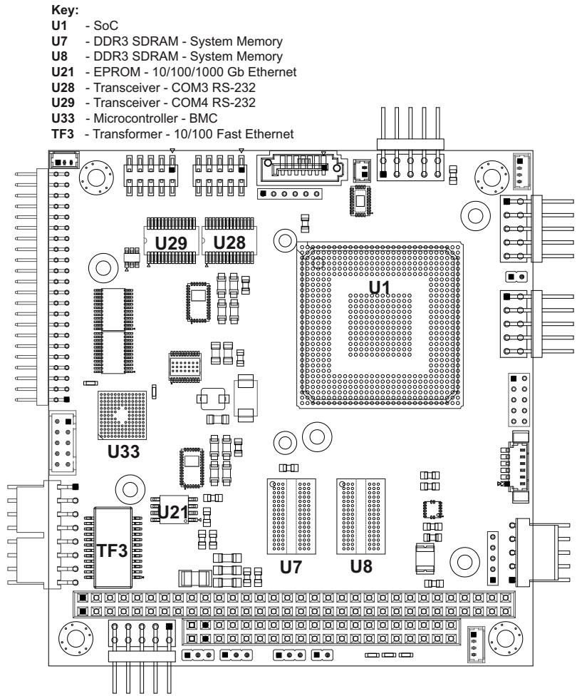
Table 2-1 describes the major ICs on the CM1-86DX3, including a brief description of each IC. Figures 2-1 and 2-2 show the locations of the major ICs.

Table 2-1: Major Component Descriptions and Functions

<table><tr><td>Chip Type</td><td>Mfg.</td><td>Model</td><td>Description</td><td>Function</td></tr><tr><td>CPU (U1)</td><td>DMP Electronics, Inc.</td><td>Vortex86-DX3</td><td>Vortex x86 6.5W, 32-bit SoC (System on Chip)</td><td>Integrates Processor Core, Graphics and Memory Controller Hub, and I/O Hub</td></tr><tr><td>DDR3L SDRAM (U7 and U8 - on top side) [see Figure 2-1]</td><td>Micron</td><td>MT41K256M16</td><td>On-board DDR3L, 1.35V, 4Gb, 32Mx16x8, non-ECC, un-buffered System Memory</td><td>Provides high-speed data transfer</td></tr><tr><td>DDR3L SDRAM (U9 and U10 - on bottom side) [see Figure 2-2]</td><td>Micron</td><td>MT41K256M16</td><td>On-board DDR3L, 1.35V, 4Gb, 32Mx16x8, non-ECC, un-buffered System Memory</td><td>Provides high-speed data transfer</td></tr><tr><td>Ethernet EEPROM (U21)</td><td>Winbond</td><td>W25Q16DVSSIG</td><td>Three-Wire Serial EEPROM for Gigabit Ethernet Controller</td><td>Provides storage for MAC addresses, serial numbers, and pre-boot configuration data</td></tr><tr><td>Ethernet Controller (U22)</td><td>Intel</td><td>WGI210IT SLIXT</td><td>Single-port Gigabit Ethernet controller</td><td>Integrates GbE MAC, PHY, and SGMII/SerDes to enable 10T/100TX/1000T Ethernet signals using the PCIe x1 bus</td></tr><tr><td>RS-485/422/232 Transceiver (U26 and U27 - on bottom side) [see Figure 2-2])</td><td>EXAR</td><td>SP339EER1-L</td><td>RS-485/422/232 Transceiver for COM1 and COM2</td><td>Transmits and receives RS-485/422/232 signals for COM1 and COM2</td></tr><tr><td>RS-232 Transceiver (U28 and U29 - on top side) [see Figure 2-1]</td><td>Analog Devices</td><td>ADM213EARSZH6ZRB</td><td>RS-232 Transceiver for COM3 and COM4</td><td>Transmits and receives RS-232 signals for COM3 and COM4</td></tr><tr><td>BMC (U33)[Optional]</td><td>Texas Instruments</td><td>TM4C123GH6ZRBT7</td><td>Microcontroller</td><td>Provides logistics and forensic information, flat panel control, I2C bus control, user flash, Watchdog Timer and fan control</td></tr><tr><td>Gb Ethernet Transformer (TF2 - on bottom side) [see Figure 2-2]</td><td>BOTHHAND</td><td>GST5009M</td><td>Gigabit Ethernet Magnetics</td><td>Provides electrical isolation for Gigabit Ethernet controller</td></tr><tr><td>Fast Ethernet Transformer (TF3 - on top side) [see Figure 2-1]</td><td>BOTHHAND</td><td>GST5009M</td><td>Fast Ethernet Magnetics</td><td>Provides electrical isolation for Fast Ethernet controller in SoC</td></tr></table>

![Key:\nU1 - SoC\nU7 - DDR3 SDRAM - System Memory\nU8 - DDR3 SDRAM - System Memory\nU21 - EPROM - 10/100/1000 Gb Ethernet\nU28 - Transceiver - COM3 RS-232\nU29 - Transceiver - COM4 RS-232\nU33 - Microcontroller - BMC\nTF3 - Transformer - 10/100 Fast Ethernet](.cm1-86dx3-50m-00084-1060-25/a7515123ba4f16d7ea3ae24f0278566233566cb9287b2abcd088e339e8e3a7b7.jpg)

Figure 2-1: Component Locations (Top Side)

# Key:

U9 - DDR3 SDRAM - System Memory
U10 - DDR3 SDRAM - System Memory
U22 - Controller - 10/100/1000 Gb Ethernet
U26 - Transceiver - COM1 RS-485/422/232
U27 - Transceiver - COM2 RS-485/422/232
TF2 - Transformer - 10/100/1000 Gb Ethernet
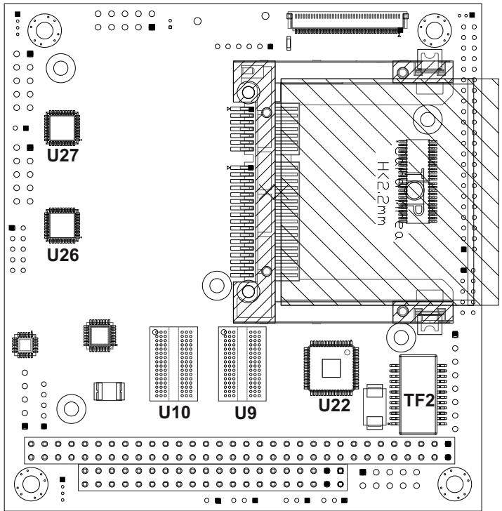
![U27\nU26\nH2233\nU10\nU9\nU22\nTF2](.cm1-86dx3-50m-00084-1060-25/a33f9bab8f0a42eef69e803f7fad35fba2c76b275a38b7faea613ce9181154fb.jpg)

Figure 2-2: Component Locations (Bottom Side)

# 2.2 Header, Connector, and Socket Definitions

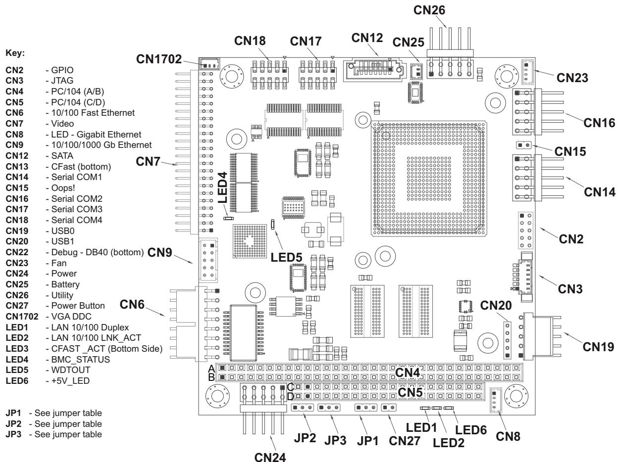
Table 2-2 describes the headers, connectors, and sockets shown in Figures 2-3 and 2-4.

Table 2-2: Header, Connector, and Socket Descriptions

<table><tr><td>Jack/Plug #</td><td>Access</td><td>Description</td></tr><tr><td>CN2 – GPIO (User)</td><td>Top</td><td>10-pin, 0.079" (2mm) header for User defined GPIO signals [TEKA, HM205CB1N-191-00]</td></tr><tr><td>CN3 – JTAG</td><td>Top</td><td>6-pin, 0.049" (1.25mm) crimp-style connector for factory use, only [WIN WIN, JS-1147V-06]</td></tr><tr><td>CN4 – PC/104 (A/B)</td><td>Top/Bottom</td><td>64-pin, 0.100" (2.54mm) connector for PC/104 (ISA) bus [EPT, 962-60322-12]</td></tr><tr><td>CN5 – PC/104 (C/D)</td><td>Top/Bottom</td><td>40-pin, 0.100" (2.54mm) connector for PC/104 (ISA) bus [EPT, 962-60202-12]</td></tr><tr><td>CN6 – 10/100 Ethernet</td><td>Top</td><td>8-pin, 0.100" (2.54mm), right-angle header for Fast (10baseT/100baseTX) Ethernet interface [MOLEX, 22-12-2084]</td></tr><tr><td>CN7 – Video</td><td>Top</td><td>44-pin, 0.079" (2mm), right-angle header for TTL/VGA interface [21N22050-44D10B-01G-4]</td></tr><tr><td>CN8 – LED - 10/100/1000 Ethernet</td><td>Top</td><td>4-pin, 0.049" (1.25mm) header for Gigabit Ethernet external LED [REGO, 830-1251-04STD-3.2-6T]</td></tr><tr><td>CN9 – 10/100/1000 Ethernet</td><td>Top</td><td>10-pin, 0.079" (2mm) header for 10/100/1000BaseT Gigabit Ethernet port [HIROSE, DF11-10DP-2DSA]</td></tr><tr><td>CN12 – SATA [Optional]</td><td>Top</td><td>7-pin, 0.050" (1.27mm), standard, right-angle connector for Generation 1 Serial ATA signals [MOLEX, 67800-5005]</td></tr><tr><td>CN13 – CFast [Optional]</td><td>Bottom</td><td>24-pin, 0.050" (1.27mm), standard, right-angle, push push socket with 8.35mm height for SATA-based CFast cards [REGO, 821101-1100190]</td></tr><tr><td>CN14 – Serial 2 (COM2)</td><td>Top</td><td>10-pin, 0.100" (2.54mm), right-angle header for Serial 2 RS485/422/232 signals [TEKA, HR205A1BB-NS-H0]</td></tr><tr><td>CN15 – Oops! Jumper</td><td>Top</td><td>2-pin, 0.079" (2mm) header for overriding current BIOS settings. Refer to Chapter 4. [JIH, 21N12050-02S10B-01G-4]</td></tr><tr><td>CN16 – Serial 1 (COM1)</td><td>Top</td><td>10-pin, 0.100" (2.54mm), right-angle header for Serial 1, RS-485/422/232 signals [TEKA, HR205A1BB-NS-H0]</td></tr><tr><td>CN17 – Serial 3 (COM3)</td><td>Top</td><td>10-pin, 0.079" (2mm), straight header for Serial 3, RS-232 signals [ASTRON, 27-24051-205-2G-TR1-R]</td></tr><tr><td>CN18 – Serial 4 (COM4)</td><td>Top</td><td>10-pin, 0.079" (2mm), straight header for Serial 4, RS-232 signals [ASTRON, 27-24051-205-2G-TR1-R]</td></tr><tr><td>CN19 – USB0</td><td>Top</td><td>5-pin, 0.100" (2.54mm), right-angle header for USB0 interface [AMP, 3-641216-5]</td></tr><tr><td>CN20 – USB1</td><td>Top</td><td>5-pin, 0.079" (2mm), straight header for USB1 interface [SAMTEC, TMM-105-03-LM-S]</td></tr><tr><td>CN22 – Debug, DB40</td><td>Bottom</td><td>40-pin, 0.196" (0.50mm) FPC/FFC, DB40 debug connector [FCI, 10042867-40MB10ELF]</td></tr><tr><td>CN23 – Fan</td><td>Top</td><td>4-pin, 0.049" (1.25mm) wire-to-board friction lock blade header for system fan signals [REGO, 830-1251-04STD-3.2-6T]</td></tr><tr><td>CN24 – Power</td><td>Top</td><td>10-pin, 0.100" (2.54mm), right-angle header for Power connection[TEKA, HR205A1BB-NS-H0]</td></tr><tr><td>CN25 – Battery</td><td>Top</td><td>2-pin, 0.049" (1.25mm) header for external battery[REGO, 830-1251-02STD-3.2-6T]</td></tr><tr><td>CN26 – Utility</td><td>Top</td><td>10-pin, 0.100" (2.54mm), right-angle header for Utility interface[TEKA, HR205A1BB-NS-H0]</td></tr><tr><td>CN27 – Power Button</td><td>Top</td><td>2-pin, 0.079" (2mm) header for external power button[JIH, 21N12050-02S10B-01G-4]</td></tr><tr><td>CN1702 – VGA DDC</td><td>Top</td><td>3-pin, 0.049" (1.25mm) header for VGA Display Data Channel[REGO, 830-1251-02STD-3.2-6T]</td></tr><tr><td>LED1 – LAN 10/100 Duplex</td><td>Top</td><td>Indicates Duplex activity of fast Ethernet interface (Green)[LIGITEK, LG-192G-CT]</td></tr><tr><td>LED2 – LAN 10/100 LNK_ACT</td><td>Top</td><td>Indicates link and traffic of fast Ethernet interface (Yellow)[EVERLIGHT, 19-21UYC/S530-A3/TR8]</td></tr><tr><td>LED3 – CFAST_ACT</td><td>Bottom</td><td>Indicates activity of CFast memory card interface (Yellow)[EVERLIGHT, 19-21UYC/S530-A3/TR8]</td></tr><tr><td>LED4 – BMC_STATUS</td><td>Top</td><td>Indicates system-error blink codes (Blue)[LIGITEK, LG-192DBK-CT/T]</td></tr><tr><td>LED5 – WDTOUT</td><td>Top</td><td>Indicates triggered watchdog timer (Red)[LIGITEK, LG-192HRF-CT]</td></tr><tr><td>LED6 – +5V_LED</td><td>Top</td><td>Indicates power on (Green)[LIGITEK, LG-192G-CT]</td></tr></table>

![Key:\nCN2 - GPIO\nCN3 - JTAG\nCN4 - PC/104 (A/B)\nCN5 - PC/104 (C/D)\nCN6 - 10/100 Fast Ethernet\nCN7 - Video\nCN8 - LED - Gigabit Ethernet\nCN9 - 10/100/1000 Gb Ethernet\nCN12 - SATA\nCN13 - CFast (bottom)\nCN14 - Serial COM1\nCN15 - Oops!\nCN16 - Serial COM2\nCN17 - Serial COM3\nCN18 - Serial COM4\nCN19 - USB0\nCN20 - USB1\nCN22 - Debug - DB40 (bottom) CN9\nCN23 - Fan\nCN24 - Power\nCN25 - Battery\nCN26 - Utility\nCN27 - Power Button CN6\nCN1702 - VGA DDC\nLED1 - LAN 10/100 Duplex\nLED2 - LAN 10/100 LNK_ACT\nLED3 - CFAST_ACT (Bottom Side)\nLED4 - BMC_STATUS\nLED5 - WDTOUT\nLED6 - +5V_LED\n\nJP1 - See jumper table\nJP2 - See jumper table\nJP3 - See jumper table\n\nCN1702 CN7 LED4 LED5 CN6 CN4 CN5 CN8 CN24 CN26 CN23 CN16 CN15 CN14 CN2 CN3 CN19\n\nA B C D E F G H I J K L M N O P Q R S T U V X Y Z A X B X C X D E F F G H I J K L M N O P Q R S T U V X Y Z A X B X C X D E F F G H I J K L M N O P Q R S T U V X Y Z A X B X C X D E F F G H I J K L M N O P Q R S T U V X Y Z A X B X C X D E F F G H I J K L M N O P Q K L M N O P Q K L M N O P Q K L M N O P Q K L M N O P Q K L M N O P Q K L M N O P Q K L M N O P Q K L M N O P Q K L M N O P Q K L M N O P Q K L M N O P Q K L M N O P Q K L M N O P Q K L M N O P Q K I N N O N O N O N O N O N O N O N O N O N O N O N O N O N O N O N O N O N O N O N O N O N O N O N O N O N O N O N O N O N O N O N O N O N O N O N O N O N O N O N O N O N O N O N O N O N O N O N O N O N O NO N\nJN2 JP3 JP1 CN27 LED2 CN8 CN24 JP2 JP3 JP1 CN27 LED2 CN8](.cm1-86dx3-50m-00084-1060-25/25d7c7680276dc95bfca39a980726aeddbab387767f18a18c5c5e026ce8499d7.jpg)

Figure 2-3: Header, Connector, and Socket Locations (Top Side)

CN13 - CFast

CN22 - Debug - DB40

CN4 - PC/104 (A/B)

LED3 - CFAST\_ACT
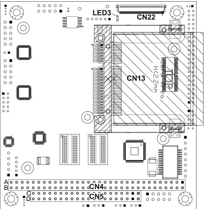
![LED3\nCN22\nCN13\nA\nB\nC\nD\nCN4\nCN5](.cm1-86dx3-50m-00084-1060-25/86aeba8f8d9a779062755ca0cb6e042231623d475d219a9ae159008bc9d934eb.jpg)

Figure 2-4: Header and Socket Locations (Bottom Side)

![The image displays a standard document icon featuring a white piece of paper with its top-right corner folded down. Faint, grey horizontal lines run across the lower portion of the paper, suggesting text. Superimposed over the document is a large, bold red checkmark that appears to have a slight motion trail or swoosh effect, extending from the bottom left upwards to the right.](.cm1-86dx3-50m-00084-1060-25/85e6906a7c9daf3ab4a225cfe6f78b03e469f5285a5b123360a185f60cfb40b6.jpg)
NOTE:

Pin 1 is shown as a solid, black square on headers and connectors.

# 2.3 Jumper Header Definitions

Table $^ { 2 - 3 }$ describes the jumper headers shown in Figure 2-5. All jumper headers provide $0 . 0 7 9 "$ (2mm) pitch.

Table 2-3: Jumper Settings

<table><tr><td>Jumper Header</td><td>Jumper on Pins 1-2</td><td>Jumper on Pins 2-3</td></tr><tr><td>JP1 – TFT Interface Voltage Select</td><td>+1.8 Volts</td><td>+3.3 Volts (Default)</td></tr><tr><td>JP2 – Backlight Voltage Select</td><td>+5 Volts</td><td>+12 Volts (Default)</td></tr><tr><td>JP3 – TFT Supply Voltage Select</td><td>+3.3 Volts (Default)</td><td>+5 Volts</td></tr></table>

Note: Remove all jumpers to set 18-bit LCD interface.

![Key:\nJP1 - TFT Interface Voltage Select\nJP2 - Backlight Voltage Select\nJP3 - TFT Supply Voltage Select\nJP2 JP3 JP1](.cm1-86dx3-50m-00084-1060-25/108e86e0dff9ec275659e356cadf09478be8bd3a180022b9055198efee229dc2.jpg)

Figure 2-5: Jumper Header Locations (Top Side)

# 2.4 Component Features

This section further describes the supported features of the CM1-86DX3 major, on-board hardware components.

# 2.4.1 CPU

The CM1-86DX3 features the DMP Electronics Vortex, Vortex86-DX3 system-on-chip (SoC). The Vortex86-DX3 is a high-performance and fully static, 32-bit x86 processor with the compatibility of Windows-based, Linux, and most popular 32-bit RTOS. The SoC integrates Processor Core, Northbridge, and Southbridge functions within a single 581-pin BGA package, providing an optimal solution for embedded system and communications products such as thin client, NAST router, home gateway, access point, and tablet applications.

# 2.4.2 SDRAM

The CM1-86DX3 employs one channel of 64-bit DDR3L on-board memory. Four SDRAM memory chips provide up to 16Gb of low-voltage non-ECC, unbuffered system memory. Refer to the MT41K SDRAM data sheet on the Micron web site.

The following total DRAM capacities are supported:

 256M x 16 x 2 = 1 GB (optional)
 256M x 16 x 4 = 2 GB (standard)

# 2.4.4 LAN Controller

The Intel I210IT provides a single-port controller that supports GbE functionality using the high-speed PCIe standard, v2.1 (2.5GT/s). The I210IT features an integrated PHY, which enables 1000BASE-T implementations such as rack-mounted or pedestal servers in add-on NIC or LAN-on-Motherboard (LOM) designs. Other implementations include blade servers such as LOMs or mezzanine cards as well as embedded applications such as switch add-on cards and network appliances. Refer to the Intel I210IT Ethernet Controller data sheet on the Intel web site.

![The image features a white document icon with a large red checkmark. Below the icon is the text 'NOTE:' in black capital letters.](.cm1-86dx3-50m-00084-1060-25/b4edb3ba4975cb368ae529c094a2fa16d8f1a760e444a34b3a302f23059ccd25.jpg)

Due to Vortex86-DX3 SoC performance limitation, Intel I210I Gigabit Ethernet will not be able to reach full bandwidth. Reliable average speed is around 550-600Mbps in full duplex mode.

# 2.4.3 CFast Card Slot

The CFast slot (CN13) provides the standard, push-push interface for CFast memory cards. LED3 provides indication of CFast activity. See Chapter 3 for the signal definitions of the CFast interface. Figure 2-6 provides the dimension and mechanical specifications of the CFast card connector.

![1.00\n37.62±0.15\n30.00±0.10\n15.00\n3.45±0.15\nREGO\nφ2.2000, hole, 2X\nφ1.80±0.10, 4X\nCARD CENTER\n35.20±0.1000\n9.50±0.1000\n4.40±0.1000\n33.66±0.0800\n45.00±0.20\n43.03±0.08\n-0.90±0.0500\n0.90±0.0500\n2.50+0.1000\n-0.0500\nCARD OVER STROKE POSITION\nCARD LOCK POSITION,\nCARD EJECTED OUT POSI\nCARD CENTER\n1.1mm (Push over stroke)\n(44.30)\n4.7mm (Eject stroke)\nCM1-86DX3_CFast conn_a](.cm1-86dx3-50m-00084-1060-25/eb2eb68d6d8d4fa4b0f09b335046c065836105c992c85c685bd995b56f4b1732.jpg)

Figure 2-6: CFast Slot

This page intentionally left blank.

# 3 Interfaces

This chapter provides descriptions and signal definitions only of the non-standard interfaces on the board. Descriptions and signal definitions of standard interfaces such as PC/104 and SATA can be found in their respective specification data sheets. If certain signals of standard interfaces have been modified or disconnected, those interfaces will be described in this chapter.

![The image displays a white document icon featuring faint horizontal lines representing text, with a large red checkmark overlaid on the left side.](.cm1-86dx3-50m-00084-1060-25/91e42591b21d7f83472cddcc9fffd43fbd50b71cbadd4445f9f4de04896db99e.jpg)
NOTE:

The tables in this chapter define pin sequence using the method in the following example: A 10-pin header with two rows of pins, using odd/even numbering, where pin 2 is directly across from pin 1, is noted as 10 pins, 2 rows, odd/even pin sequence (1, 2). Consecutive numbering is noted, for example, as 24 pins, 2 rows, consecutive pin sequence (1, 13), where pin 13 is directly across from pin 1. Refer to Figure 2-3 and Figure 2-4 for pin-1 locations.

# 3.1 Serial Interfaces

Table 3-1 provides the signals for serial interfaces 1 & 2. Table 3-2 provides the signals for the serial interfaces 3 & 4. Both interfaces use 10-pin, right-angle headers with 2 rows, odd/even sequence (1, 2), and 0.100" (2.54mm) pitch.

![The image displays a stylized icon of a white document or file. On the left side, there are three short, horizontal black lines representing text. Dominating the center is a large, bold red checkmark (or tick) that appears slightly blurred or has a shadow effect, suggesting a sense of completion or approval.](.cm1-86dx3-50m-00084-1060-25/3ffe259fdfdf0514de20bb323e86370b3150134aeb056abfcf1f93bb8a993f4f.jpg)
NOTE:

Serial Ports 1 and 2 provide RS-485/422 functions as well as RS-232 functionality. Only pins 1 and 3 provide RS-485/422/232 signals. Pins 5 and 7 provide only RS-422/232 signals.

To change the mode from RS-232 to RS-485 or RS-422, use the settings in the Advanced>Serial Port menu of the BIOS Setup Utility, described in Chapter 4.

In Table 3-1, pins 1, 3, 5, and 7 include secondary signals assigned for RS-485/422 modes.

Serial Ports 3 and 4, described in Table 3-2, provide only RS-232 functions.

Table 3-1: Serial Port 1 (CN16) & Port 2 (CN14) Interface Pin Signals

<table><tr><td>Pin #</td><td>Signal</td><td>DB9 #</td><td>Description</td></tr><tr><td rowspan="2">1</td><td>DCD*</td><td>1</td><td>Data Carrier Detect – Indicates external serial device is detecting a carrier signal (i.e., a communication channel is currently open). In direct connect environments, this input is driven by DTR as part of the DTR/DSR handshake.</td></tr><tr><td>TX-/RX-</td><td></td><td>If in RS-422 mode, this pin is TX- (Data Negative). If in RS-485 mode, this pin is TX-/RX- (Data Negative).</td></tr><tr><td>2</td><td>DSR*</td><td>6</td><td>Data Set Ready – Indicates external serial device is powered, initialized, and ready. Used as hardware handshake with DTR for overall readiness.</td></tr><tr><td rowspan="2">3</td><td>RXD</td><td>2</td><td>Receive Data – Serial port receive data input is typically held at a logic 1 (mark) when no data is being transmitted, and is held “Off” for a brief interval after an “On” to “Off” transition on the RTS line to allow the transmission to complete.</td></tr><tr><td>TX+/RX+</td><td></td><td>If in RS-422 mode, this pin is TX+ (Data Positive). If in RS-485 mode, this pin is TX+/RX+ (Data Positive).</td></tr><tr><td>4</td><td>RTS*</td><td>7</td><td>Request To Send – Indicates serial port is ready to transmit data. Used as hardware handshake with CTS for low level flow control.</td></tr><tr><td rowspan="2">5</td><td>TXD</td><td>3</td><td>Transmit Data – Serial port transmit data output is typically held to a logic 1 when no data is being sent. Typically, a logic 0 (On) must be present on RTS, CTS, DSR, and DTR before data can be transmitted on this line.</td></tr><tr><td>RX+</td><td></td><td>If in RS-422 mode, this pin is RX+ (Data Positive).</td></tr><tr><td>6</td><td>CTS*</td><td>8</td><td>Clear To Send – Indicates external serial device is ready to receive data. Used as hardware handshake with RTS for low level flow control.</td></tr><tr><td rowspan="2">7</td><td>DTR*</td><td>4</td><td>Data Terminal Ready – Indicates serial port is powered, initialized, and ready. Used as hardware handshake with DSR for overall readiness.</td></tr><tr><td>RX-</td><td></td><td>If in RS-422 mode, this pin is RX- (Data Negative).</td></tr><tr><td>8</td><td>RI*</td><td>9</td><td>Ring Indicator – Indicates external serial device is detecting a ring condition. Used by software to initiate operations to answer and open the communications channel.</td></tr><tr><td>9</td><td>GND</td><td>5</td><td>Ground</td></tr><tr><td>10</td><td>Key/NC</td><td>NC</td><td>Key Pin/Not connected</td></tr></table>

Note: The shaded table cells denote power or ground. The \* symbol indicates the signal is Active Low.

Table 3-2: Serial Port 3 (CN17) & Port 4 (CN18) Interface Pin Signals

<table><tr><td>Pin #</td><td>Signal</td><td>DB9 #</td><td>Description</td></tr><tr><td>1</td><td>DCD*</td><td>1</td><td>Data Carrier Detect – Indicates external serial device is detecting a carrier signal (i.e., a communication channel is currently open). In direct connect environments, this input is driven by DTR as part of the DTR/DSR handshake.</td></tr><tr><td>2</td><td>DSR*</td><td>6</td><td>Data Set Ready – Indicates external serial device is powered, initialized, and ready. Used as hardware handshake with DTR for overall readiness.</td></tr><tr><td>3</td><td>RXD</td><td>2</td><td>Receive Data – Serial port receive data input is typically held at a logic 1 (mark) when no data is being transmitted, and is held “Off” for a brief interval after an “On” to “Off” transition on the RTS line to allow the transmission to complete.</td></tr><tr><td>4</td><td>RTS*</td><td>7</td><td>Request To Send – Indicates serial port is ready to transmit data. Used as hardware handshake with CTS for low level flow control.</td></tr><tr><td>5</td><td>TXD</td><td>3</td><td>Transmit Data – Serial port transmit data output is typically held to a logic 1 when no data is being sent. Typically, a logic 0 (On) must be present on RTS, CTS, DSR, and DTR before data can be transmitted on this line.</td></tr><tr><td>6</td><td>CTS*</td><td>8</td><td>Clear To Send – Indicates external serial device is ready to receive data. Used as hardware handshake with RTS for low level flow control.</td></tr><tr><td>7</td><td>DTR*</td><td>4</td><td>Data Terminal Ready – Indicates serial port is powered, initialized, and ready. Used as hardware handshake with DSR for overall readiness.</td></tr><tr><td>8</td><td>RI*</td><td>9</td><td>Ring Indicator – Indicates external serial device is detecting a ring condition. Used by software to initiate operations to answer and open the communications channel.</td></tr><tr><td>9</td><td>GND</td><td>5</td><td>Ground</td></tr><tr><td>10</td><td>Key/NC</td><td>NC</td><td>Key Pin – Not connected</td></tr></table>

Note: The shaded table cells denote power or ground. The \* symbol indicates the signal is Active Low.

# 3.2 USB Interfaces

The CM1-86DX3 provides one root USB hub and two functional USB ports, supporting USB EHCI v2.0 and over-current detection.

Table 3-3 describes the pin signals of the USB0 interface, which uses a single-row, 5-pin, right-angle header with 0.100" (2.54mm) pitch.

Table 3-3: USB0 Interface Pin Signals (CN19)

<table><tr><td>Pin #</td><td>Signal</td><td>Description</td></tr><tr><td>1</td><td>USB0PWR</td><td>USB Power – VCC (+5V +/-5%) power goes to the port through an on-board fuse. Port is disabled if this input is low.</td></tr><tr><td>2</td><td>USB0N</td><td>USB0 Port Data Negative</td></tr><tr><td>3</td><td>USB0P</td><td>USB0 Port Data Positive</td></tr><tr><td>4</td><td>GND</td><td>USB0 Port ground</td></tr><tr><td>5</td><td>SHIELD</td><td>USB0 Port shield</td></tr></table>

Note: The shaded table cells denote power or ground.
Table 3-4 describes the pin signals of the USB1 interface, which uses a single-row, 5-pin, vertical header with 0.079" (2mm) pitch.

Table 3-4: USB1 Interface Pin Signals (CN20)

<table><tr><td>Pin #</td><td>Signal</td><td>Description</td></tr><tr><td>1</td><td>USB1PWR</td><td>USB Power – VCC (+5V +/-5%) power goes to the port through an on-board fuse. Port is disabled if this input is low.</td></tr><tr><td>2</td><td>USB1N</td><td>USB1 Port Data Negative</td></tr><tr><td>3</td><td>USB1P</td><td>USB1 Port Data Positive</td></tr><tr><td>4</td><td>GND</td><td>USB1 Port ground</td></tr><tr><td>5</td><td>SHIELD</td><td>USB1 Port shield</td></tr></table>

Note: The shaded table cells denote power or ground.

# 3.3 Utility Interface

The Utility interface provides various utility and I/O signals on the module and consists of a 10-pin, 0.1" (2.54mm) pitch header. The Vortex CPU drives the signals on the Utility interface, and Table 3-5 provides the signal definitions.

 PS/2 Keyboard and PS/2 Mouse
 Battery
 Reset Switch
 Speaker

# 3.3.1 Keyboard

The signal lines for a PS/2 keyboard are provided from the Vortex CPU to the Utility interface.

# 3.3.2 Mouse

The signal lines for a PS/2 mouse are provided from the Vortex CPU to the Utility interface.

# 3.3.3 Battery

An external battery input connection is provided through the Utility interface to support a battery backup for the CMOS RAM and the RTC (Real Time Clock).

# 3.3.4 Reset Switch

An external reset switch provides the reset signal through the Utility interface to a reset circuit, which drives the Vortex CPU.

# 3.3.5 Speaker

The speaker signal provides sufficient signal strength to drive a 1W 8  “Beep” speaker through the Utility interface at an audible level. The speaker signal is driven from an on-board amplifier and the Vortex CPU.

Table 3-5 describes the pin signals of the Utility interface, which uses a 10-pin, right-angle header with 2 rows, odd/even sequence (1, 2), and 0.100" (2.54mm) pitch.

Table 3-5: Utility Interface Pin Signals (CN26)

<table><tr><td>Pin #</td><td>Signal</td><td>Description</td></tr><tr><td>1</td><td>SPKR</td><td>Speaker Output</td></tr><tr><td>2</td><td>GND</td><td>Ground</td></tr><tr><td>3</td><td>RST_BTN_IN*</td><td>External Reset Switch signal</td></tr><tr><td>4</td><td>MSDATA</td><td>Mouse Data input</td></tr><tr><td>5</td><td>KBDATA</td><td>Keyboard Data input</td></tr><tr><td>6</td><td>KBCLK</td><td>Keyboard Clock input</td></tr><tr><td>7</td><td>GND</td><td>Ground</td></tr><tr><td>8</td><td>+VCC UTIL</td><td>Keyboard /Mouse power (+5V) output</td></tr><tr><td>9</td><td>VBATV_EX</td><td>Real time battery voltage (3.6V Type/ 4.0V Max) input</td></tr><tr><td>10</td><td>MSCLK</td><td>Mouse Clock input</td></tr></table>

Note: The shaded table cells denote power or ground. The \* symbol indicates the signal is Active Low.

# 3.4 Fast Ethernet Interface

Table 3-6 describes the pin signals of the Fast Ethernet interface, which uses a single-row, 8-pin header with 0.100" (2.54mm) pitch.

Table 3-6: Fast Ethernet Interface Pin Signals (CN6)

<table><tr><td>Pin #</td><td>Signal</td><td>Description</td></tr><tr><td>1</td><td>LAN100_TX_P</td><td rowspan="2">Analog Twisted Pair Ethernet Transmit Differential Pair – These pins transmit the serial bit stream through the isolation transformer.</td></tr><tr><td>2</td><td>LAN100_TX_N</td></tr><tr><td>3</td><td>LAN100_RX_P</td><td rowspan="2">Analog Twisted Pair Ethernet Receive Differential Pair – These pins receive the serial bit stream through the isolation transformer.</td></tr><tr><td>6</td><td>LAN100_RX_N</td></tr><tr><td>4</td><td>ETH_PE</td><td rowspan="2">Connected through two 75 ohm resistors in series to center tap of isolation transformer and then to ground through common 1k PF capacitor.</td></tr><tr><td>5</td><td>ETH_PE</td></tr><tr><td>7</td><td>ETH_PE</td><td rowspan="2">Connected through two 75 ohm resistors in series to center tap of isolation transformer and then to ground through common 1k PF capacitor.</td></tr><tr><td>8</td><td>ETH_PE</td></tr></table>

# 3.5 Gigabit Ethernet Interface

Table 3-7 describes the pin signals of the Gigabit Ethernet header which consists of 10 right-angle pins, two rows, odd/even (1,2) pin sequence, and 0.079" (2mm) pitch.

Table 3-7: Gigabit Ethernet Interface Pin Signals (CN9)

<table><tr><td>Pin #</td><td>Signal</td><td>Description</td></tr><tr><td>1</td><td>ETH-PE</td><td rowspan="2">Connected through two 75 ohm resistors in series to center tap of isolation transformer and then to ground through common 1k PF capacitor.</td></tr><tr><td>2</td><td>ETH-PE</td></tr><tr><td>3</td><td>ETH1_TRD0_P</td><td rowspan="2">Media Dependent Interface 0 +/-</td></tr><tr><td>4</td><td>ETH1_TRD0_N</td></tr><tr><td>5</td><td>ETH1_TRD1_P</td><td rowspan="2">Media Dependent Interface 1 +/-</td></tr><tr><td>6</td><td>ETH1_TRD1_N</td></tr><tr><td>7</td><td>ETH1_TRD2_P</td><td rowspan="2">Media Dependent Interface 2 +/-</td></tr><tr><td>8</td><td>ETH1_TRD2_N</td></tr><tr><td>9</td><td>ETH1_TRD3_P</td><td rowspan="2">Media Dependent Interface 3 +/-</td></tr><tr><td>10</td><td>ETH1_TRD3_N</td></tr></table>

Note: The shaded table cells denote ground.

# 3.6 Gigabit Ethernet External LED Interface

Table 3-8 defines the signals of the external LED that indicates Gigabit Ethernet links and activity using a single row of 4 pins with 0.049" (1.25mm) pitch.

Table 3-8: Gigabit Ethernet External LED Pin Signals (CN8)

<table><tr><td>Pin #</td><td>Signal</td><td>Description</td></tr><tr><td>1</td><td>+V3P3</td><td>+3.3 volts Power</td></tr><tr><td>2</td><td>ETH1_LINK_ACT*</td><td>Indicates link connectivity or transfer data activity</td></tr><tr><td>3</td><td>ETH1_LED_100*</td><td>Indicates link activity at 100 Mbps</td></tr><tr><td>4</td><td>ETH1_LED_1000*</td><td>Indicates link activity at 1000 Mbps</td></tr></table>

Note: The shaded table cell denotes power. The \* symbol indicates the signal is Active Low.

# 3.7 Video (TFT/VGA) Interface

Table 3-9 describes the pin signals of the Video interface, which uses a 44-pin, right-angle header with 2 rows, odd/even sequence (1, 2), and 0.079" (2mm) pitch.

Note: The shaded table cells denote power or ground.
Table 3-9: Video Interface Pin Signals (CN7)

<table><tr><td>Pin #</td><td>Signal</td><td>Description</td></tr><tr><td>1</td><td>FP1_CLK</td><td>TFT Shift Clock – This clock signal provides the timing for transferring digital pixel data.</td></tr><tr><td>2</td><td>FP1_DE</td><td>TFT Data Enable – This signal indicates valid data on any of the FP [23:0] lines.</td></tr><tr><td>3</td><td>FP1_HSYNC</td><td>TFT Line Pulse – This signal is the digital monitor equivalent of HSYNC.</td></tr><tr><td>4</td><td>FP1_VSYNC</td><td>TFT Frame Marker – This signal is the TFT monitor equivalent of VSYNC.</td></tr><tr><td>5</td><td>GND1</td><td>Ground 1</td></tr><tr><td>6</td><td>GND2</td><td>Ground 2</td></tr><tr><td>7</td><td>NC</td><td>Not connected (FP0 = Flat Panel Data 0)</td></tr><tr><td>8</td><td>NC</td><td>Not connected (FP1 = Flat Panel Data 1)</td></tr><tr><td>9</td><td>FP2</td><td>Flat Panel Data 2 – data output, Blue0 (18-bit)</td></tr><tr><td>10</td><td>FP3</td><td>Flat Panel Data 3 – data output, Blue1 (18-bit)</td></tr><tr><td>11</td><td>FP4</td><td>Flat Panel Data 4 – data output, Blue2 (18-bit)</td></tr><tr><td>12</td><td>FP5</td><td>Flat Panel Data 5 – data output, Blue3 (18-bit)</td></tr><tr><td>13</td><td>FP6</td><td>Flat Panel Data 6 – data output, Blue4 (18-bit)</td></tr><tr><td>14</td><td>FP7</td><td>Flat Panel Data 7 – data output, Blue5 (18-bit)</td></tr><tr><td>15</td><td>NC</td><td>Not connected (FP8 = Flat Panel Data 8)</td></tr><tr><td>16</td><td>NC</td><td>Not connected (FP9 = Flat Panel Data 9)</td></tr><tr><td>17</td><td>FP10</td><td>Flat Panel Data 10 – data output, Green0 (18-bit)</td></tr><tr><td>18</td><td>FP11</td><td>Flat Panel Data 11 – data output, Green1 (18-bit)</td></tr><tr><td>19</td><td>FP12</td><td>Flat Panel Data 12 – data output, Green2 (18-bit)</td></tr><tr><td>20</td><td>FP13</td><td>Flat Panel Data 13 – data output, Green3 (18-bit)</td></tr><tr><td>21</td><td>FP14</td><td>Flat Panel Data 14 – data output, Green4 (18-bit)</td></tr><tr><td>22</td><td>FP15</td><td>Flat Panel Data 15 – data output, Green5 (18-bit)</td></tr><tr><td>23</td><td>NC</td><td>Not connected (FP16 = Flat Panel Data 16)</td></tr><tr><td>24</td><td>NC</td><td>Not connected (FP17 = Flat Panel Data 17)</td></tr><tr><td>25</td><td>FP18</td><td>Flat Panel Data 18 – data output, Red0 (18-bit)</td></tr><tr><td>26</td><td>FP19</td><td>Flat Panel Data 19 – data output, Red1 (18-bit)</td></tr><tr><td>27</td><td>FP20</td><td>Flat Panel Data 20 – data output, Red2 (18-bit)</td></tr><tr><td>28</td><td>FP21</td><td>Flat Panel Data 21 – data output, Red3 (18-bit)</td></tr><tr><td>29</td><td>FP22</td><td>Flat Panel Data 22 – data output, Red4 (18-bit)</td></tr><tr><td>30</td><td>FP23</td><td>Flat Panel Data 23 – data output, Red5 (18-bit)</td></tr><tr><td>31</td><td>VDD_EN_CN</td><td>TFT Power Enable</td></tr><tr><td>32</td><td>BKLT_EN_R</td><td>TFT Backlight Enable</td></tr><tr><td>33</td><td>+VCC_TFT_CN</td><td>Panel Voltage (+3.3 or +5 volts ±5%) depending on setting of JP3</td></tr><tr><td>34</td><td>+VCC_BKL_CN</td><td>Backlight Voltage (+5 or +12 volts ±5%) depending on setting of JP2</td></tr><tr><td>35</td><td>GND3</td><td>Ground 3</td></tr><tr><td>36</td><td>GND4</td><td>Ground 4</td></tr><tr><td>37</td><td>CON_HSYNC</td><td>Horizontal Sync – This signal is used for the digital horizontal sync output to the CRT. Also used (with VSYNC) to signal power management state information to the CRT per the VESATM DPMSTM standard.</td></tr><tr><td>38</td><td>CON_VSYNC</td><td>Vertical Sync – This signal is used for the digital vertical sync output to the CRT. Also used (with HSYNC) to signal power management state information to the CRT per the VESATM DPMSTM standard.</td></tr><tr><td>39</td><td>AGNDR</td><td>Analog Ground for Red</td></tr><tr><td>40</td><td>VGA_RED</td><td>Red – This pin provides the Red analog output to the CRT.</td></tr><tr><td>41</td><td>AGNDG</td><td>Analog Ground for Green</td></tr><tr><td>42</td><td>VGA_GREEN</td><td>Green – This pin provides the Green analog output to the CRT.</td></tr><tr><td>43</td><td>AGNDB</td><td>Analog Ground for Blue</td></tr><tr><td>44</td><td>VGA_BLUE</td><td>Blue – This pin provides the Blue analog output to the CRT.</td></tr></table>

# 3.8 VGA DDC (Display Data Channel)

The VGA DDC interface provides digital communication of display modes between the display and a graphics adapter for plug-and-play performance, enabling the computer host to adjust monitor parameters such as brightness and contrast.

Table 3-10 describes the signals for the VGA DDC interface, which provides a single row, 3-pin header with 0.049" (1.25mm) pitch.

Table 3-10: VGA DDC Signals (CN1702)

<table><tr><td>Pin #</td><td>Signal</td><td>Description</td></tr><tr><td>1</td><td>VGA_DDC_CLK</td><td>Display Data Channel clock</td></tr><tr><td>2</td><td>NC</td><td>Not Connected</td></tr><tr><td>5</td><td>VGA_DDC_DAT</td><td>Display Data Channel data</td></tr></table>

# 3.9 Power Interface

The CM1-86DX3 requires one +5 volt DC power source. If the +5VDC power drops below \~4.65V, a low voltage reset is triggered, resetting the system.

The power input header (CN24) supplies the following voltages and ground directly to the module:

 5.0VDC +/- 5% @ 1.35 Amps

Table 3-11 describes the pin signals of the Power interface, which uses a 10-pin, right-angle header with 2 rows, odd/even sequence (1, 2), and 0.100" (2.54mm) pitch.

Table 3-11: Power Interface Pin Signal (CN24)

<table><tr><td>Pin</td><td>Signal</td><td>Descriptions</td></tr><tr><td>1</td><td>+5V</td><td>+5 Volts</td></tr><tr><td>2</td><td>GND</td><td>Ground</td></tr><tr><td>3</td><td>+5V</td><td>+5 Volts</td></tr><tr><td>4</td><td>GND</td><td>Ground</td></tr><tr><td>5</td><td>NC</td><td>Not Connected</td></tr><tr><td>6</td><td>GND</td><td>Ground</td></tr><tr><td>7</td><td>+12V</td><td>+12 volts routed to PC/104</td></tr><tr><td>8</td><td>GND</td><td>Ground</td></tr><tr><td>9</td><td>+5V</td><td>+5 Volts</td></tr><tr><td>10</td><td>GND</td><td>Ground</td></tr></table>

Note: The shaded table cells denote power or ground.

# 3.10 Battery Interface

Table 3-12 lists the pin signals of the External Battery Input header for backup RTC (Real Time Clock), which uses 2 pins with 0.049" (1.25mm) pitch.

Table 3-12: External Battery Input Header (CN25)

<table><tr><td>Pin #</td><td>Signal</td><td>Description</td></tr><tr><td>1</td><td>VBAT_EXT</td><td>+3.0 volts DC</td></tr><tr><td>2</td><td>GND</td><td>Ground</td></tr></table>

Note: The shaded table cells denote power or ground. The RTC has an expected current draw of \~5A at room temperature $( 2 5 ^ { \circ } \mathsf { C } )$ . A 3-volt model (CR1225) battery is recommended. The battery is used only when power is not applied to the board.

# 3.11 Power Button Interface

Table 3-13 lists the pin signals of the External Power Button header, which uses 2 pins with 0.079" (2mm) pitch.

Table 3-13: External Power Button Header (CN27)

<table><tr><td>Pin #</td><td>Signal</td><td>Description</td></tr><tr><td>1</td><td>PWRBTN#</td><td>+3.3 volts for power button</td></tr><tr><td>2</td><td>GND</td><td>Ground</td></tr></table>

Note: The shaded table cells denote power or ground.

# 3.12 CFast Mass Storage Socket

The optional CFast socket supports Generation 1 SATA signals with transfer speeds of 1.5 GB/s and is compatible with versions 1.1 and 2.0 CFast cards. This 24-pin female socket provides 7 data pins and 17 power pins for CFast Type II mass storage cards.

Table 3-14 lists the pin signals of the CFast Card socket, which uses 24 right-angle pins with 0.050" (1.27mm) pitch.

Table 3-14: CFast Mass Storage Socket (CN13)

<table><tr><td>Pin #</td><td>Signal</td><td>Description</td></tr><tr><td>S1</td><td>SGND</td><td>Ground</td></tr><tr><td>S2</td><td>CFAST_C_TX_P</td><td>SATA HOST Signal Pair</td></tr><tr><td>S3</td><td>CFAST_C_TX_N</td><td>SATA HOST Signal Pair</td></tr><tr><td>S4</td><td>SGND</td><td>Ground</td></tr><tr><td>S5</td><td>CFAST_C_RX_N</td><td>SATA HOST Signal Pair</td></tr><tr><td>S6</td><td>CFAST_C_RX_P</td><td>SATA HOST Signal Pair</td></tr><tr><td>S7</td><td>SGND</td><td>Ground</td></tr><tr><td colspan="3">Key</td></tr><tr><td>PC1</td><td>NC</td><td>Not Connected</td></tr><tr><td>PC2</td><td>GND</td><td>Ground</td></tr><tr><td>PC3</td><td>NC</td><td>Not Connected</td></tr><tr><td>PC4</td><td>NC</td><td>Not Connected</td></tr><tr><td>PC5</td><td>NC</td><td>Not Connected</td></tr><tr><td>PC6</td><td>NC</td><td>Not Connected</td></tr><tr><td>PC7</td><td>GND</td><td>Ground</td></tr><tr><td>PC8</td><td>CFAST_ACT#</td><td>Card Activity LED</td></tr><tr><td>PC9</td><td>NC</td><td>Not Connected</td></tr><tr><td>PC10</td><td>NC</td><td>Not Connected</td></tr><tr><td>PC11</td><td>NC</td><td>Not Connected</td></tr><tr><td>PC12</td><td>NC</td><td>Not Connected</td></tr><tr><td>PC13</td><td>PWR1</td><td>+3.3V</td></tr><tr><td>PC14</td><td>PWR2</td><td>+3.3V</td></tr><tr><td>PC15</td><td>PGND</td><td>Power / Ground</td></tr><tr><td>PC16</td><td>PGND</td><td>Power / Ground</td></tr><tr><td>PC17</td><td>NC</td><td>Not Connected</td></tr></table>

Note: The shaded table cells denote power or ground.

This page intentionally left blank.

# 4 Utilities

# 4.1 BIOS Setup

The CM1-86DX3 features an AMI BIOS. The default settings provide a “ready to run” system, even without a BIOS setup backup battery.

The BIOS is located in flash memory and can be easily updated with software under DOS.

All setup changes of the BIOS are stored in the CMOS RAM.

The soldered battery will provide power to store that information for over two years without board activation.

# 4.1.1 Configuring the BIOS

 Pressing &lt;DEL&gt; during power up starts the BIOS setup utility.
 Pressing &lt;F11&gt; during power up starts the boot menu.

# 4.1.2 Main screen of the BIOS

The main screen of the BIOS SETUP UTILITY gives you a quick overview of the BIOS version, the clock speed, installed memory, memory speed, date and time. The date and time can be configured by the user.

![Main Advanced Boot Security Exit\n* System Overview\n* **********\n* System Time (10:47:05)\n* System Date (Tue 08/25/2015)\n* System Firmware Version\n* System BIOS :097\n* Build Date :08/24/2015\n* VGA BIOS :0.00.01\n* Processor\n* Type :RDC(R) R3600\n* Speed :1000MHz\n* System Memory\n* Size :1984MB\n* Speed :667MHz\n* Use (ENTER), (TAB)\n* or (SHIFT-TAB) to\n* select a field.\n*\n* Use (+) or (-) to\n* configure system Date.\n*\n*\n*\n*\n*\n*\n*\n*\n*\n*\n*\n*\n*\n*\n*\n*\n*\n*\n*\n*\n*\n*\n*\n*\n*\n*\n*\n*\n*\n*\n*\n*\n*\n*\n*\n*\n*\n*\n*\n*\n*\n*\n*\n*\n*\n*\n*\n*\n*\n*\n*\n*\n*\n*\n*\nv02.67 (C)Copyright 1985-2009, American Megatrends, Inc.](.cm1-86dx3-50m-00084-1060-25/cb72b5ec0261295cb22d5b2ebc147aefdb725384b59fef100e0e575b7ace7599.jpg)

# 4.1.3 Advanced Settings screen

The main screen of “Advanced Settings” provides configuration settings for the IDE interface, serial port, remote access, and USB port. Refer to the following illustrations for visual reference. A description of the selected setting appears in the right column of the active screen.

![The image displays a yellow triangular warning sign with a black border. Inside the triangle is a black exclamation point. Below the triangle is a black rectangular bar containing the text 'CAUTION:' in white capital letters.](.cm1-86dx3-50m-00084-1060-25/58d6ef09b002c39935885e8718fc3bebbaac340f2997b733bf06b7478ee8765e.jpg)
MISE EN GARDE

The use of inappropriate values on any of the following advanced settings below may cause the system to malfunction.

L'utilisation de valeurs inappropriées sur l'un des paramètres avancés suivants ci-dessous peut entraîner un dysfonctionnement du système.

![Main Advanced Boot Security Exit\n* Advanced Settings\n* **********\n* WARNING: Setting wrong values in below sections\n* may cause system to malfunction.\n* * SATA Configuration\n* * Serial Port Configuration\n* * Remote Access Configuration\n* * USB Configuration\n* * Select Screen\n* ** Select Item\n* Enter Go to Sub Screen\n* F1 General Help\n* F10 Save and Exit\n* ESC Exit\n*\n*\n*\n*\n*\n*\n*\n*\n*\n*\n*\n*\n*\n*\n*\n*\n*\n*\n*\n*\n*\n*\n*\n*\n*\n*\n*\n*\n*\n*\n*\n*\n*\n*\n*\nv02.67 (C)Copyright 1985-2009, American Megatrends, Inc.](.cm1-86dx3-50m-00084-1060-25/b206ae8815517aabcd8c206d69e6f06b44b3d71c814c861fdc14ad56a532223f.jpg)

# Advanced > IDE Configuration

These settings allow you to configure the features of the integrated IDE controllers.

![Advanced\n*\nIDE Configuration\n*\n*SATA Controller : (Not Detected)\n*\nHard Disk Delay (Disabled)\nSelect HDD Type (SATA)\n*\n* While entering setup,\n* BIOS auto detects the\n* presence of SATA\n* devices. This displays\n* the status of auto\n* detection of SATA\n* devices.\n*\n*\n*\n*\n*\n*\n*\n*\n*\n*\n* Select Screen\n* ** Select Item\n* Enter Go to Sub Screen\n* F1 General Help\n* F10 Save and Exit\n* ESC Exit\n*\n*\n*\n*\nv02.67 (C)Copyright 1985-2009, American Megatrends, Inc.](.cm1-86dx3-50m-00084-1060-25/55001cdcc98e46dbe4709598a12cc1ab30043dbcf66f459a943c0f424820fa0f.jpg)

# Advanced > IDE Master

This setting provides options for IDE slave and master drives.

![Advanced\n* Secondary IDE Master\n* **********\n* Device :Not Detected\n* **********\n* Type (Auto)\n* LBA/Large Mode (Auto)\n* Block (Multi-Sector Transfer) (Auto)\n* PIO Mode (Auto)\n* DMA Mode (Auto)\n* S.M.A.R.T. (Auto)\n* 32Bit Data Transfer (Enabled)\n* Select the type\n* of device connected\n* to the system.\n*\n*\n*\n*\n*\n*\n*\n*\n*\n*\n*\n*\n*\n*\n*\n*\n*\n*\n*\n*\n*\n*\n*\n*\n*\n*\n*\n*\n*\n*\n*\n*\n*\n*\n*\n*\n*\n*\n*\n*\n*\n*\n*\n*\n*\n*\n*\n*\n*\n*\n*\n*\n*\n*\n*\n*\n*\n*\n*\n*\n*\n*\n*\n*\n*\n*\n*\n*\n*\n*\n*\n*\n*\nv02.67 (C)Copyright 1985-2009, American Megatrends, Inc.](.cm1-86dx3-50m-00084-1060-25/b7549fee52938f3ec36bb48203e72cd5d4c86852b913e121b5523f34ee3ff8f3.jpg)

# Advanced > Serial Port

These settings allow you to specify the base I/O port address, Interrupt Request address, and Port Type mode (if applicable) of specific serial ports.

![Advanced\n**********************************************************************\n* SB Serial Port 1\n* Serial Port IRQ\n* Serial Port Type\n* SB Serial Port 2\n* Serial Port IRQ\n* Serial Port Type\n* SB Serial Port 3\n* Serial Port IRQ\n* SB Serial Port 4\n* Serial Port IRQ\n(3F8)\n(IRQ4)\n(RS-232)\n(2F8)\n(IRQ3)\n(RS-232)\n(3E8)\n(IRQ6)\n(2E8)\n(IRQ7)\n* RDC Internal UART\n* Serial Port\n*\n*\n*\n*\n*\n*\n*\n*\n*\n*\n*\n*\n*\n*\n*\n*\n*\n*\n*\n*\n*\n*\n*\n*\n*\n*\n*\n*\n*\n*\n*\n*\n*\n*\n*\n*\n*\n*\n*\n*\n*\n*\n*\n*\n*\n*\n*\n*\n*\n*\n*\n*\n*\n*\n*\n*\n*\n*\n*\n*\n*\n*\n*\n*\n*\n*\n*\n*\n*\n*\n*\n*\n*\n*\n*\n*\n*\n*\n*\n*\n*\n*\n*\n*\nv02.67 (C)Copyright 1985-2009, American Megatrends, Inc.](.cm1-86dx3-50m-00084-1060-25/8e4d0e5a1e6c1afe24396f10fff9cd7f457e1da08fc4ec8ddf7ca54a09111422.jpg)

# Advanced > Remote Access

Remote Access allows you to enter the BIOS Setup through a serial terminal or PC.

![Advanced\n* Configure Remote Access type and parameters\n* *****\n* Remote Access (Enabled)\n*\n* Serial port number (COM2)\n* Base Address, IRQ (2F8h, 3)\n* Serial Port Mode (115200 8,n,1)\n* Flow Control (None)\n* Redirection After BIOS POST (Always)\n* Terminal Type (ANSI)\n* VT-UTF8 Combo Key Support (Enabled)\n* Sredir Memory Display Delay (No Delay)\n*\n* Select Remote Access type.\n*\n*\n* Select Screen\n*\n** Select Item\n*\n+- Change Option\n*\n* F1 General Help\n*\n* F10 Save and Exit\n*\nESC Exit\n*\n*\n*\nv02.67 (C)Copyright 1985-2009, American Megatrends, Inc.](.cm1-86dx3-50m-00084-1060-25/1b1759830ed740c101b1b659fbe072e57297ef824520c64a4ab1b86ceb6a3d6b.jpg)

# Advanced > USB Port

The USB Support settings allow you to select options for enabling or disabling on-board USB ports. The Legacy USB support settings allow a USB mouse and keyboard to control the system even if no USB drivers are loaded on the system.

![Advanced\n* USB Configuration\n* Mechanical Mechanical Mechanical Mechanical Mechanical Mechanical Mechanical Mechanical Mechanical Mechanical Mechanical Mechanical Mechanical Mechanical Mechanical Mechanical Mechanical Mechanical Mechanical Mechanical Mechanical Mechanical Mechanical Mechanical Mechanical Mechanical Mechanical Mechanical Mechanical Mechanical Mechanical Mechanical Mechanical Mechanical Mechanical Mechanical Mechanical Mechanical Mechanical Mechanical Mechanical Mechanical Mechanical Mechanical Mechanical Mechanical Mechanical Mechanical Mechanical Mechanical Mechanical Mechanical Mechanical Mechanical Mechanical Mechanical Mechanical Mechanical Mechanical Mechanical Mechanical Mechanical Mechanical Mechanical Mechanical Mechanical Mechanical Mechanical Mechanical Mechanical Mechanical Mechanical Mechanical Mechanical Mechanical Mechanical Mechanical Mechanical Mechanical Mechanical Mechanical Mechanical Mechanical Mechanical Mechanical Mechanical Mechanical Mechanical Mechanical Mechanical Mechanical Mechanical Mechanical Mechanical Mechanical Mechanical Mechanical Mechanical Mechanical Mechanical Machinery\n* * * * * * * * * * * * * * * * * * * * * * * * * * * * * * * * * * * * * * * * * * * * * * * * * * * * * * * * * * * * * * * * * * * * * * * * * * * * * * * * * * * * * * * * * * * * * * * * * * * * * *\n*  Use the following three lines:\n*  Use the following three lines:\n*  Use the following three lines:\n*  Use the following three lines:\n*  Use the following three lines:\n*  Use the following three lines:\n*  Use the following three lines:\n*  Use the following three lines:\n*  Use the following three lines:\n*  Use the following three lines:\n*  Use the following three lines:\n*  Use the following three lines:\n*  Use the following three lines:\n*  Use it from the following three lines:\n*  Use the following three lines:\n*  Use the following three lines:\n*  Use the following three lines:\n*  Use the following three lines:\n*  Use the following three lines:\n*  Use the following three lines:\n*  Use the following three lines:\n*  Use the following three lines:\n*  Use the following three lines:\n*  Use the following three lines:\n*  Use the following three lines:\n*  Use the following three line:\n*  Use the following three line:\n*  Use the following three line:\n*  Use the following three line:\n*  Use the following three line:\n*  Use the following three line:\n*  Use the following three line:\n*  Use the following three line:\n*  Use the following three line:\n*  Use the following three line:\n*  Use the following three line:\n*  Use the following three line:\n*  Use the following three line:\n*  Utilization of a specific physical component (e.g., thermal conductivity or temperature) in a module with respect to a specific physical component (e.g., thermal conductivity or temperature). The module version - 3.0.0-14.4\n*  Use the following four lines:\n*  Use the following four lines:\n*  Use the following four lines:\n*  Use the following four lines:\n*  Use the following four lines:\n*  Use the following four lines:\n*  Use the following four lines:\n*  Use the following four lines:\n*  Use the following four lines:\n*  Use the following four lines:\n*  Use the following four lines:\n*  Use the following four lines:\n*  Use the following four lines:\n*  Use it from the following four lines:\n*  Use it from the following four lines:\n*  Use it from the following four lines:\n*  Use it from the following four lines:\n*  Use it from the following four lines:\n*  Use it from the following four lines:\n*  Use it from the following four lines:\n*  Use it from the following four lines:\n*  Use it from the following four lines:\n*  Use it from the following four lines:\n*  Use it, from the following one line:\n*  Use it, from the following one line:\n*  Use it, from the following one line:\n*  Use it, from the following one line:\n*  Use it, from the following one line:\n*  Use it, from the following one line:\n*  Use it, from the following one line:\n*  Use it, from the following one line:\n*  Use it, from the following one line:\n*  Use it, from the following one line:](.cm1-86dx3-50m-00084-1060-25/bcdfb9796dfcdbb0740adbb47246daac77e88eac97de1c392a2dc7f4a90f5e0c.jpg)

# 4.1.4 Boot screen

If more than one drive is attached to the CM1-86DX3, you can select from the first “Boot Settings” screen the boot order in which the drives are scanned for a bootable OS image.

# Boot Settings

The Boot From LAN setting allows you to enable LAN PXE boot. The Boot Display Device setting allows you to choose CRT or LCD as the display source.

![Main Advanced Boot Security Exit\n**********************************************************************\n* Boot Settings\n* **************\n* * Boot Device Priority\n* Boot From LAN (Disabled)\n* Boot Display Device (CRT)\n**********************************************************************\n**********************************************************************\n**********************************************************************\n**********************************************************************\n**********************************************************************\n**********************************************************************\n**********************************************************************\n**********************************************************************\n**********************************************************************\n**********************************************************************\n**********************************************************************\n**********************************************************************\n**********************************************************************\n**********************************************************************\n**********************************************************************\n**********************************************************************\n**********************************************************************\n**********************************************************************\n**********************************************************************\n**********************************************************************\n**********************************************************************\n**********************************************************************\n**********************************************************************\n**********************************************************************\n**********************************************************************\n**********************************************************************\n**********************************************************************\n**********************************************************************\n**********************************************************************\n**********************************************************************\n**********************************************************************\n**********************************************************************\n**********************************************************************\n**********************************************************************\n**********************************************************************\n**********************************************************************\n**********************************************************************\n**********************************************************************\n**********************************************************************\n**********************************************************************\n**********************************************************************\n**********************************************************************\n**********************************************************************\n**********************************************************************\n**********************************************************************\n**********************************************************************\n**********************************************************************\n**********************************************************************\n**********************************************************************\n**********************************************************************\n**************************************************************** Strength\n* Select Screen\n* ** Select Item\n* Enter Go to Sub Screen\n* F1 General Help\n* F10 Save and Exit\n* ESC Exit\n* \n* \n********************************************************************** v02.67 (C)Copyright 1985-2009, American Megatrends, Inc.](.cm1-86dx3-50m-00084-1060-25/fdfcaa84146d9ab59f3d5b7fe780035e4a60eeec6ccbba0153930ac7d9fbec06.jpg)

# Boot > Boot Device Priority

These settings allow you to specify the order in which the system checks for the device from which to boot.

![Boot\n**********************************************************************\n* Boot Device Priority\n* **************\n* 1st Boot Device (Removable Dev.)\n* 2nd Boot Device (CD/DVD)\n* 3rd Boot Device (Hard Drive)\n* 4th Boot Device (USB)\n* 5th Boot Device (Network)\n**********************************************************************\n* Specifies the boot *\n* sequence from the\n* available devices.\n*\n* A device enclosed in\n* parenthesis has been\n* disabled in the\n* corresponding type\n* menu.\n*\n*\n*\n*\n*\n* Select Screen\n* ** Select Item\n* +- Change Option\n* F1 General Help\n* F10 Save and Exit\n* ESC Exit\n**********************************************************************\nv02.67 (C)Copyright 1985-2009, American Megatrends, Inc.](.cm1-86dx3-50m-00084-1060-25/c7b55276baf5470e89589a561c8122df6e0194dbd3bf8bc82e4b72b2c628282f.jpg)

# 4.1.5 Security screen

This screen allows you to set a Supervisor or a User password. If you want to use both passwords, the Supervisor password must be set first.

![Main Advanced Boot Security Exit\n* Security Settings\n* **********\n* Supervisor Password :Not Installed\n* User Password :Not Installed\n* Change Supervisor Password\n* Change User Password\n* Install or Change the *\n* password.\n*\n*\n*\n*\n*\n*\n*\n*\n*\n* Select Screen\n*\n** Select Item\n*\nEnter Change\n*\nF1 General Help\n*\nF10 Save and Exit\n*\nESC Exit\n*\n*\n*\nv02.67 (C)Copyright 1985-2009, American Megatrends, Inc.](.cm1-86dx3-50m-00084-1060-25/5352ff74172316f75be7a592a7971f8d9e2c1dd059f538852bb65feebb762010.jpg)

# 4.1.6 Exit screen

The settings in the Exit screen allow you to exit the BIOS Setup utility while saving or discarding certain defaults or changes.

![Main Advanced Boot Security Exit\n**********************************************************************\n* Exit Options\n* **************\n* Save Changes and Exit\n* Discard Changes and Exit\n* Discard Changes\n*\n* Load Optimal Defaults\n* Load Failsafe Defaults\n*\n*\n*\n*\n*\n*\n*\n*\n*\n*\n*\n*\n*\n*\n*\n*\n*\n*\n*\n*\n*\n*\n*\n*\n*\n*\n*\n*\n*\n*\n*\n*\n*\n*\n*\n*\n*\n*\n*\n*\n*\n*\n*\n*\n*\n*\n*\n*\n*\n*\n*\n*\n*\n*\n*\n*\n*\n*\n*\n*\n*\n*\n*\n*\n*\n*\n*\n*\n*\n*\n*\n*\n*\n*\n*\n*\n*\n*\n*\n*\n*\n*\n*\n*\n*\n*\nv02.67 (C)Copyright 1985-2009, American Megatrends, Inc.](.cm1-86dx3-50m-00084-1060-25/87167a63683d44c8e2f60b6cc6ae9bbc6325141a101442f622f236b3f7b084d1.jpg)

# 4.2 SEMA Functions

Under the management of the BMC chip (Board Management Controller), the SEMA utility (Smart Embedded Management Agent) provides system control and failure protection—counting, monitoring, and measuring hardware and software events, from which the SoC can trigger corrective commands. The optional SEMA Cloud utility not only controls local events on the module but system client events on the Internet of Things (IoT.) Refer to the following bullets for a list of SEMA functions.

 Total operating hours counter Counts the time the module has been run in minutes.
 On-time minutes counter Counts the seconds since last system start.
 Monitoring of Board temperature Minimum and maximum temperature values of the board are stored in flash.
 Power monitor Reads the current drawn by the board and reports the nominal operating voltage.
 Power cycles counter
 Boot counter Boot counter is increased after a HW- or SW-Reset or after a successful power-up.
Watchdog Timer Set / Reset / Disable Watchdog Timer.
 System Restart Cause Power loss / Watchdog / External Reset.
 Flash area 1kB Flash area for customer data
 Protected Flash area 128 Bytes for Keys, ID's, etc. can be stored in a write- and clear-protectable region.
 Board Identify Vendor / Board / Serial number

The SEMA Tools are available for Windows and Linux. SEMA functionality can also be used in applications. Refer to the SEMA software manual and technical manual on the ADLINK web site for more information.

![The image displays a graphic icon of a white document with a folded top-right corner and faint horizontal lines. A large red checkmark is superimposed over the document. Below the graphic, the text 'NOTE:' appears in bold, black capital letters.](.cm1-86dx3-50m-00084-1060-25/7268183bd755b2a98a796f3ae67612d0903aa3bbe1845eaf3c24c536970bcd88.jpg)

If a failure occurs while updating the BMC firmware through the SEMA command line, restart the system and repeat the update to resolve the failure.

# 4.2.1 Board Specific SEMA functions

# Voltages

The BMC of the CM1-86DX3 implements a Voltage Monitor and samples several Onboard Voltages. The Voltages can be read by calling the SEMA function, “Get Voltages”. The function returns a 16-bit value divided in Hi-Byte (MSB) and Lo-Byte (LSB).

Table 4-1: SEMA Monitored Voltages

<table><tr><td>ADC Channel</td><td>Voltage Name</td><td>Voltage Formula [V]</td></tr><tr><td>0</td><td>VCC_CORE</td><td>(MSB&lt;&lt;8 + LSB) x 3.3 / 1024</td></tr><tr><td>1</td><td>V1P2</td><td>(MSB&lt;&lt;8 + LSB) x 3.3 / 1024</td></tr><tr><td>2</td><td>VTT</td><td>(MSB&lt;&lt;8 + LSB) x 3.3 / 1024</td></tr><tr><td>3</td><td>VDDQ</td><td>(MSB&lt;&lt;8 + LSB) x 3.3 / 1024</td></tr><tr><td>4</td><td>V1P8</td><td>(MSB&lt;&lt;8 + LSB) x 3.3 / 1024</td></tr><tr><td>5</td><td>V3P3</td><td>(MSB&lt;&lt;8 + LSB) x 1.1 x 3.3 / 1024</td></tr><tr><td>6</td><td>VCC</td><td>(MSB&lt;&lt;8 + LSB) x 1.83 x 3.3 / 1024</td></tr><tr><td>7</td><td>V12</td><td>(MSB&lt;&lt;8 + LSB) x 6.0 x 3.3 / 1024</td></tr><tr><td>8</td><td>MAINCURRENT</td><td>Use Main Current Function</td></tr></table>

# Main Current

The BMC of the CM1-86DX3 implements a Current Monitor. The current can be read by calling the SEMA function “Get Main Current”. The function returns four 16-bit values divided in Hi-Byte (MSB) and Lo-Byte (LSB). These four values represent the last four currents drawn by the board. The values are sampled every 250ms. The order of the four values is NOT in relationship to time. The access to the BMC may increase the drawn current of the whole system. In this case, you still have three samples without the influence of the read access.

$$
\text { Main   Current } = (\text { MSB\_n } &lt;   &lt;   8 + \text { LSB\_n }) * 8. 0 6 \mathrm{mA}
$$

# TS#-Events

TS# is activated by a temperature sensor when a device reaches its critical temperature and released when the device is back in its normal temperature range. This counter gives the user information about temperature or cooling issues. This counter is cleared when the system is removed from power. The CM1-86DX3 only monitors the board temperature and does not support TS#-Events.

# Exception Blink Codes

In the case of an error, the BMC shows a blink code on the STATUS-LED. This error code is also reported by the BMC Flags register. The Exception Code is not stored in the Flash storage and is cleared when the power is removed. Therefore, the “Clear Exception Code”-Command is not supported.

Table 4-2: Blink Codes

&lt;table&gt;<tr><td>Exception Blink Code</td><td>Error Message</td></tr><tr><td>0</td><td>NOERROR</td></tr><tr><td>2</td><td>NO_VCORE_POK_3P3</td></tr><tr><td>3</td><td>NO_V1P2_POK_3P3</td></tr><tr><td>4</td><td>NO_VDDQ_POK_3P3</td></tr><tr><td>5</td><td>NO_V1P8_POK_3P3</td></tr><tr><td>6</td><td>NO_V3P3_POK_3P3</td></tr><tr><td>7</td><td>CRITICAL_TEMP</td></tr><tr><td>8</td><td>POWER_FAIL</td></tr><tr><td>9</td><td>VOLTAGE_FAIL</td></tr><tr><td>10</td><td>NO_BUF_PLT_RST_L</td></tr></table>

# BMC Flags

The BMC Flags register returns the last detected exception code since power up.

# 4.3 Real Time Clock (RTC)

The CM1-86DX3 contains a Real Time (time of day) Clock (RTC), which can be backed up with an external Lithium Battery. The CM1-86DX3 will function without a battery in those environments which prohibit batteries. The CM1-86DX3 will also continue to operate after the battery life has been exceeded. Under these conditions all setup information is restored from the onboard flash memory during POST along with the default date and time information.

![The image displays a document icon featuring a white sheet of paper with a folded upper-right corner and faint horizontal lines indicating text. A large red checkmark is superimposed over the center of the document.](.cm1-86dx3-50m-00084-1060-25/e1e49cb2b5523f9bafc0520389a14e9c8e708b36417a35cf3ceb1ad579041d8b.jpg)
NOTE:

Some operating systems require a valid default date and time to function.

# 4.4 User GPIO Interface

Table 4-3 describes the pin signals of the GPIO interface, which uses a 10-pin header with 2 rows, odd/even sequence (1, 2), and 0.079" (2mm) pitch.

Table 4-3: User GPIO Interface Pin Signals (CN2)

<table><tr><td>Pin #</td><td>Signal</td><td>Description</td></tr><tr><td>1</td><td>GPIO0</td><td>User defined</td></tr><tr><td>2</td><td>GPIO1</td><td>User defined</td></tr><tr><td>3</td><td>GPIO2</td><td>User defined</td></tr><tr><td>4</td><td>GPIO3</td><td>User defined</td></tr><tr><td>5</td><td>GPIO4</td><td>User defined</td></tr><tr><td>6</td><td>GPIO5</td><td>User defined</td></tr><tr><td>7</td><td>GPIO6</td><td>User defined</td></tr><tr><td>8</td><td>GPIO7</td><td>User defined</td></tr><tr><td>9</td><td>GND</td><td>Ground</td></tr><tr><td>10</td><td>GND</td><td>Ground</td></tr></table>

Note: The shaded table cells denote ground.

# 4.5 Oops! Jumper (BIOS Recovery)

The Oops! jumper is provided in the event you have selected BIOS settings that prevent you from booting the system. By using the Oops! Jumper you can stop the current BIOS settings in the CMOS from being loaded, allowing you to proceed, using the default settings. Install a jumper on the CN15, 2-pin header or connect the DTR pin to the RI pin on Serial port 1 (COM 1) prior to boot up to prevent the present BIOS settings from loading. After booting with the Oops! Jumper in place, remove the Oops! Jumper and go into the BIOS Setup Utility. Change the desired BIOS settings, or select the default settings, and save changes before rebooting the system.

To convert a standard DB9 connector to an Oops! Jumper, short together the DTR (4) and RI (9) pins on the rear of the connector as shown in the following figure on the Serial Port 1 DB9 connector.

![Standard DB9 Serial\nPort Connector (Female)\nRear View\n1 2 3 4 5\n6 7 8 9\nCM1-86DX3_Oopsjump_](.cm1-86dx3-50m-00084-1060-25/94f6e6a85d265518a3d5f9587e0687c5b9857540040c0aabcb984fee6e7d3095.jpg)

# 4.6 Serial Console

The CM1-86DX3 BIOS supports the serial console (or console redirection) feature. These I/O functions are provided by an ANSI-compatible serial terminal, or the equivalent terminal emulation software running on another system. This can be very useful when setting up the BIOS on a production line for systems that are not connected to a keyboard and display.

# 4.7 Serial Console BIOS Setup

The serial console (console redirection) feature is implemented by connecting a standard nullmodem cable or a modified serial cable (or “Hot Cable”) from either serial port COM1 or COM2 (CN14 or CN16) to the serial terminal or a PC with communications software. The BIOS Setup Utility controls the serial console settings on the CM1-86DX3. Refer to the BIOS Setup for the serial console option settings using a serial terminal or PC with communications software.

# 4.8 Hot (Serial) Cable

To convert a standard serial cable to a Hot Cable, certain pins must be shorted together at the Serial port header or at the DB9 connector. Short together the RTS (4) and RI (8) pins on either the COM1 or COM2 (CN14 or CN16) header. As an alternate, you can short the equivalent pins (pins 7 and 9) on the back of the respective DB9 connector as shown in the following figure.

![Serial Port Header\n(COM1 or COM2)\nOr\nStandard DB9 Serial\nPort Connector (Female)\nRear View\n(or Front View of\nMale Connector)\nCM1-86DX3_HotCable_a](.cm1-86dx3-50m-00084-1060-25/a1d9541d081bfe3e4b765d9603c18b58ff84b7b20ad5afaba34387e5ba44ae3c.jpg)

# 4.9 Watchdog Timer

The Watchdog Timer (WDT) restarts the system if an error or mishap occurs, allowing the system to recover from the mishap, even though the error condition may still exist. Possible problems include failure to boot properly, loss of control by the application software, failure of an interface device, unexpected conditions on the bus, or other hardware or software malfunctions.

The WDT is used through the SEMA during normal system operation. The following SEMA features provide support for the WDT.

 ADLINK SEMA provides an API for the WDT. The API tickles (resets) the WDT before the timer expires, otherwise the system will be reset.
Watchdog Code examples – ADLINK has provided source code examples in the CM1-86DX3 SEMA, illustrating how to control the WDT. The code examples can be easily copied to your environment to compile and test, or to make any desired changes before compiling. Refer to the SEMA Programming Guide by downloading the SEMA Utility from the CM1-86DX3 web page.

# Appendix A System Resources

This appendix provides system resource specifications for the CM1-86DX3 including Memory addresses, IO addresses, PCI configuration registers, IO registers, and system interrupts.

# A.1 Memory Address Map

The SoC supports 4 GBytes of addressable memory space and 64 KBytes of addressable I/O space. In order to be compatible with a PC/AT system, the lower 1 MBytes of this addressable memory is divided into regions which can be individually controlled with programmable attributes such as disable, read/write, write only, or read only.

Figure 2 represents the SoC memory address map. It shows the main memory regions defined and supported by the SoC. At the highest level, the address space is divided into two main conceptual regions. One is the 0-1-Mbyte DOS Compatibility region, and the other is the 1-Mbyte to 4-GByte Extended Memory region.

# DOS Compatibility Region

The first region of memory is called the DOS Compatibility Region and it was defined for early PCs.This area is divided into the following address regions:

 0-640 KByte DOS Area
 640-768 KByte Video Buffer Area
 768-896 KByte in 16 KByte section (total of 8 section)-Expansion Area
 896-960 KByte in 16 KByte section (total of 4 section)-Expansion System BIOS Area
 960 KByte-1Mbyte Memory (BIOS Area)-System BIOS Area

# DOS Area (00000-9FFFFFh)

The DOS area (0000H-9FFFFh) is 640 KBytes in Size. It is mapped to the main memory controlled by the SoC.

# Video Buffer Area (A0000-BFFFFh)

The 128 KByte graphics adapter memory region is normally mapped to a video device on the PCI bus (Typically VGA controller). This area is controlled by the A/B Page control Register. It can be mapped to either the main DRAM or the PCI bus for both read and write commands.

# ISA Expansion Area (C0000–DFFFFh)

This 128-KByte ISA Expansion region is divided into eight 16-KByte segments. Each segment can be assigned one of four Read/Write states: read-only, write-only, read/write, or disabled. Typically, these blocks are mapped through the PCI bridge to ISA space. Memory that is disabled is not remapped.

# Extended System BIOS (E0000–EFFFFh)

This 64-KByte area is divided into four 16-KByte segments. Each segment can be assigned independent read and write attributes so it can be mapped either to the main DRAM or to the PCI bus. Typically, this area is used for RAM or ROM. Memory that is disabled is not remapped.

# System BIOS Area (F0000–FFFFFh)

This area is a single 64-KByte segment that can be assigned read and write attributes. It is by default (after reset) read/write disabled and cycles are forwarded to the PCI bus. By manipulating the read/write attributes, the SoC can “shadow” BIOS into main memory. Memory that is disabled is not remapped.

# Extended Memory Region

This memory region covers 10\_0000h (1 Mbyte) to FFFF\_FFFFh (4 GBytes minus 1) address range and is divided into the following regions:

 DRAM memory from 1 Mbyte to the top of memory
 PCI Memory space from the top of memory to 4 GBytes
 High BIOS area from 4 GBytes to 4 GBytes minus 16 MBytes

# Main DRAM Address Range (0010\_0000h to Top of Main Memory)

The address range from 1 Mbyte to the top of main memory is mapped to the main memory address range controlled by the SoC. All accesses to addresses within this range are forwarded to the main memory.

# PCI Memory Address Range (Top of Main Memory to 4 GBytes)

The address range from the top of main DRAM to 4 GBytes is normally mapped to PCI. The PMC forwards all accesses within this address range to PCI.

# High BIOS Area (FF00\_0000–FFFF\_FFFFh)

The top 16 MBytes of the Extended Memory Region is reserved for System BIOS (High BIOS), extended BIOS for PCI devices, and the A20 alias of the system BIOS. The CPU begins execution from the High BIOS after reset. This region is mapped to the PCI so that the upper subset of this region is aliased to 16 MBytes minus 256 KBytes range. The actual address space required for the BIOS is less than 2 MBytes. However, the minimum CPU MTRR range for this region is 2 MBytes. Thus, the full 2 MBytes must be considered.

![Based on the provided flowchart/block diagram, here is the accurate description of the labeled blocks and connections:\n\n**Left Column (Memory Hierarchy):**\n*   **Top Label:** '4GB'\n*   **Upper Block:** 'PCI Memory'\n*   **Divider Label:** 'Top of memory' (horizontal line)\n*   **Side Label (Middle):** 'Main Memory' (indicated by vertical arrows)\n*   **Bottom Block:** 'DOS Compatibility Memory'\n*   **Bottom Label:** '0KB'\n*   **Boundary Label:** '1MB' (next to the top of the DOS block)\n*   **Side Label (Top):** 'Extended Memory' (indicated by vertical arrows)\n\n**Right Column (Memory Map):**\n*   **Top Block:** 'Upper BIOS Area (64 KB)' associated with address '0FFFFFh'\n*   **Second Block:** 'Lower BIOS Area (64 KB) 16KB*4' associated with addresses '0F0000h' and '0EFFFFh'\n*   **Third Block:** 'Expansion Card BIOS and Buffer Area (128 KB) 16KB*8' associated with addresses '0E0000h' and '0DFFFFh'\n*   **Fourth Block:** 'Standard PCI/ISA Video Memory (SMM Mem) 128 KB' associated with addresses '0C0000h' and '0BFFFFh'\n*   **Fifth Block:** 'DOS Area (640 KB)' associated with addresses '0A0000h' and '09FFFFh'\n*   **Bottom Label:** '000000h'\n*   **Far Right Scale Labels (Top to Bottom):** '1MB', '960KB', '896KB', '768KB', '640KB', '0KB'\n\n**Connections:**\n*   A dotted line connects '0KB' (bottom left) to '000000h' (bottom right).\n*   A long diagonal dotted line connects '1MB' (top of the DOS block on the left) to '0F0000h' (top of the Lower BIOS Area on the right).](.cm1-86dx3-50m-00084-1060-25/c3b9b51877f086ffb7b568214a7e89412be4606a2f2104ca1e8b64f7c7ac225f.jpg)

Figure B-2: Memory Address Map

# A.2 I/O Address Map

The SoC positively decodes accesses to all internal registers, including PCI configuration registers (CF8h and CFCh), PC/AT Compatible IO registers (8237, 8254 & 8259), and all re-locatable IO space registers (UART).

Table A-1: Fixed IO Ranges in the CPU

<table><tr><td>Device</td><td>IO Address</td><td>Comment</td></tr><tr><td>DMA 8237-1</td><td>0000h – 000Fh</td><td></td></tr><tr><td>PIC 8259-1</td><td>0020h – 0021h</td><td></td></tr><tr><td>Indirect Access Registers (6117D configuration port)</td><td>0022h – 0023h</td><td></td></tr><tr><td>Timer Counter 8254</td><td>0040h –0043h</td><td></td></tr><tr><td>Keyboard / Mouse data port</td><td>0060h</td><td></td></tr><tr><td>Port B + NMI control port</td><td>0061h</td><td></td></tr><tr><td>8051 download 4k address counter</td><td>0062h – 0063h</td><td></td></tr><tr><td>Keyboard/ Mouse status/ command port</td><td>0064h</td><td></td></tr><tr><td>WatchDog0 reload counter</td><td>0065h</td><td></td></tr><tr><td>CMOS RAM port</td><td>0070h – 0071h</td><td></td></tr><tr><td>MTBF control register</td><td>0072h – 0075h</td><td></td></tr><tr><td>DMA page register</td><td>0080h – 008Fh</td><td></td></tr><tr><td>System control register</td><td>0092h</td><td></td></tr><tr><td>PIC 8259-2</td><td>00A0h – 00A1h</td><td></td></tr><tr><td>WatchDog1 control counter</td><td>00A8h – 00ADh</td><td></td></tr><tr><td>WatchDog1 reload counter</td><td>00AEh</td><td></td></tr><tr><td>DMA 8237-2</td><td>00C0h – 00DFh</td><td></td></tr><tr><td>DOS 4G Page access</td><td>00E0h – 00EFh</td><td></td></tr><tr><td>IDE 1(IRQ 15)</td><td>0170h – 0177h</td><td></td></tr><tr><td>COM4 (IRQ 11)</td><td>02E8h – 02EFh</td><td></td></tr><tr><td>COM2 (IRQ 3)</td><td>02F8h – 02EFh</td><td></td></tr><tr><td>COM3 (IRQ 10)</td><td>03E8h – 03EFh</td><td></td></tr><tr><td>IDE1 ATAPI device control write only register</td><td>03F6h</td><td></td></tr><tr><td>COM1 (IRQ 4)</td><td>03F8h – 03FFh</td><td></td></tr><tr><td>DMA High page register</td><td>0480h – 048Fh</td><td></td></tr><tr><td>Instruction counter register</td><td>0490h – 0499h</td><td></td></tr><tr><td>Instruction counter register</td><td>0490h – 0499h</td><td></td></tr><tr><td>8259 Edge / level control register</td><td>04D0h – 04D1h</td><td></td></tr><tr><td>PCI configuration port</td><td>0CF8h – 0CFFh</td><td></td></tr><tr><td>PCA9535 GPIO Controller</td><td>40h</td><td>On I2C Bus</td></tr></table>

![This image features a graphic of a white document with a folded corner and faint horizontal lines, overlaid with a large red checkmark. Below the graphic, the text 'NOTE:' is written in bold black capital letters.](.cm1-86dx3-50m-00084-1060-25/09afb39d0767942c44b4b2269c081e207c3de911477f7366de5355a05927bff8.jpg)

The following table shows the variable IO decode ranges. They are set using base address registers (BARs) or other similar means. Plug-and-play (PnP) software (PCI/ACPI) can use their configuration mechanisms to set and adjust these values.

Table A-2: Variable IO Address Ranges Decoded by PCI Devices in the IO Fabric

<table><tr><td>Device</td><td>Size / Bytes</td><td>Comment</td></tr><tr><td>ACPI Power Management (PCU)</td><td>128</td><td>ACPI BASE ADDRESS: PCI[B:0,D:7,F:0] + F8h</td></tr><tr><td>I2C</td><td>16</td><td>I2C BASE ADDRESS: PCI[B:0,D:7,F:0] + D4h</td></tr></table>

![The image displays a standard warning sign featuring a yellow triangle with a black border. Inside the triangle is a black exclamation point. Below the triangle is a black rectangular bar containing the white text 'CAUTION:'.](.cm1-86dx3-50m-00084-1060-25/202423933a7fad89a90626d2e71374e96772d2e81af3f985bf5f4454191ce975.jpg)
MISE EN GARDE

Variable IO ranges should not be set to conflict with other IO ranges. There will be unpredictable results if the configuration software allows conflicts to occur. Hardware does not check for conflicts.

Les plages d'E/S variables ne doivent pas être définies pour entrer en conflit avec d'autres plages d'E/S. Il y aura des résultats imprévisibles si le logiciel de configuration permet à des conflits de se produire. Le matériel ne recherche pas les conflits.

# A.3 PCI Configuration Registers

Devices and functions can be accessed by the PCI Configuration Registers.

Table A-3: PCI Configuration Registers

<table><tr><td>Address Range (hex)</td><td>Description</td></tr><tr><td>0CFB – 0CF8</td><td>PCI Configuration Address Register</td></tr><tr><td>0CFF – 0CFC</td><td>PCI Configuration Data Register</td></tr></table>

Table A-4: PCI CONFIG\_ADDRESS Register Mapping (IO Port CF8h)

<table><tr><td>Field</td><td>CONFIG_ADDRESS Bits</td></tr><tr><td>Enable PCI Configuration Space Mapping</td><td>31</td></tr><tr><td>Reserved</td><td>30:24</td></tr><tr><td>Bus Number</td><td>23:16</td></tr><tr><td>Device Number</td><td>15:11</td></tr><tr><td>Function Number</td><td>10:08</td></tr><tr><td>Register / Offset Number</td><td>07:02</td></tr></table>

![The image displays a digital icon of a white document tilted slightly to the left. Faint grey horizontal lines simulate text on the page, and a large red checkmark with a thick outline is superimposed on the upper right corner of the document.](.cm1-86dx3-50m-00084-1060-25/2e9c59e61498452e22f280557159c3437b8e9776d85269e211af1fcee9809e91.jpg)
NOTE:

Bit 31 of CONFIG\_ADDRESS must be set for a configuration cycle to be generated.

Table A-5: PCI Devices and Functions

<table><tr><td>Bus#</td><td>Device#</td><td>Function#</td><td>Device ID</td><td>Description</td><td>Function</td></tr><tr><td>0</td><td>0</td><td>0</td><td>6023h</td><td>Host bridge</td><td></td></tr><tr><td>0</td><td>1</td><td>0</td><td>1031h</td><td>PCI-to-PCI bridge(PCI Express)</td><td></td></tr><tr><td>0</td><td>2</td><td>0</td><td>1031h</td><td>PCI-to-PCI bridge(PCI Express)</td><td></td></tr><tr><td>0</td><td>7</td><td>0</td><td>6035</td><td>ISA bridge</td><td></td></tr><tr><td>0</td><td>7</td><td>1</td><td>6035h</td><td>ISA bridge</td><td></td></tr><tr><td>0</td><td>8</td><td>0</td><td>6040h</td><td>Ethernet controller</td><td></td></tr><tr><td>0</td><td>A</td><td>0</td><td>6060h</td><td>USB OHCI</td><td></td></tr><tr><td>0</td><td>A</td><td>1</td><td>6061h</td><td>USB2 EHCI</td><td></td></tr><tr><td>0</td><td>C</td><td>0</td><td>1012h</td><td>IDE controller</td><td></td></tr><tr><td>0</td><td>D</td><td>0</td><td>2015</td><td>VGA controller</td><td></td></tr><tr><td>1</td><td>0</td><td>0</td><td>1533h</td><td>Intel Ethernet controller</td><td></td></tr></table>

# A.4 IO Register Maps

# A.4.1 CMOS Memory and RTC Registers

The RTC internal registers and RAM are organized as two banks of 128 bytes each, called the standard and extended banks. The first 14 bytes of the standard bank contain the RTC time and date information along with four registers A-D, that are used for configuration of the RTC. The extended bank contains a full 128 bytes of battery backed SRAM. All data movement between the host CPU and the RTC is done through register mapped standard I/O space.

![The image shows a white document icon with a folded top-right corner. Inside the document, there are faint horizontal lines. A large red checkmark is superimposed over the document. Below the icon, the text 'NOTE:' is written in black capital letters.](.cm1-86dx3-50m-00084-1060-25/87b3cb52192947e1c9b06eae2732ee57c5c618928b48f3b407ef3193f77d01f7.jpg)

It is not possible to disable the extended bank.

![The image displays a graphic icon of a white document with a folded top-right corner and faint horizontal lines. A large red checkmark is superimposed on the document. Below the graphic, the text 'NOTE:' appears in black, capital letters.](.cm1-86dx3-50m-00084-1060-25/df29c04afd143ed9ce0dac1fd4ca31aae4bfafee2c712d8583bbbd84fe0251e6.jpg)

Registers reg\_RTC\_IR\_type and reg\_RTC\_TR\_type are used for data movement to and from the standard bank.

Table A-6: RTC IO Registers Alias Locations

<table><tr><td>Register</td><td>Original IO location</td></tr><tr><td>reg_RTC_IR_type</td><td>70h</td></tr><tr><td>reg_RTC_TR_type</td><td>71h</td></tr></table>

Table A-7: RTC Indexed Registers

<table><tr><td>Start</td><td>End</td><td>Name</td></tr><tr><td>00h</td><td>00h</td><td>Seconds</td></tr><tr><td>01h</td><td>01h</td><td>Seconds Alarm</td></tr><tr><td>02h</td><td>02h</td><td>Minutes</td></tr><tr><td>03h</td><td>03h</td><td>Minutes Alarm</td></tr><tr><td>04h</td><td>04h</td><td>Hours</td></tr><tr><td>05h</td><td>05h</td><td>Hours Alarm</td></tr><tr><td>06h</td><td>06h</td><td>Day of Week</td></tr><tr><td>07h</td><td>07h</td><td>Day of Month</td></tr><tr><td>08h</td><td>08h</td><td>Month</td></tr><tr><td>09h</td><td>09h</td><td>Year</td></tr><tr><td>0Ah</td><td>0Ah</td><td>Register A</td></tr><tr><td>0Bh</td><td>0Bh</td><td>Register B</td></tr><tr><td>0Ch</td><td>0Ch</td><td>Register C</td></tr><tr><td>0Dh</td><td>0Dh</td><td>Register D</td></tr><tr><td>0Eh</td><td>7Fh</td><td>114 Bytes of User RAM</td></tr><tr><td>09h</td><td>09h</td><td>Year</td></tr><tr><td>0Ah</td><td>0Ah</td><td>Register A</td></tr><tr><td>0Bh</td><td>0Bh</td><td>Register B</td></tr><tr><td>0Ch</td><td>0Ch</td><td>Register C</td></tr><tr><td>0Dh</td><td>0Dh</td><td>Register D</td></tr><tr><td>0Eh</td><td>7Fh</td><td>114 Bytes of User RAM</td></tr></table>

# A.5 Interrupts

# A.5.1 SERIRQ Interrupt Mapping

Below the SERIRQ Interrupt Mapping is shown:

Table A-8: SERRIRQ Interrupt Mapping

<table><tr><td>Data Frame#</td><td>Interrupt</td><td>Comment</td></tr><tr><td>1</td><td>IRQ0</td><td>System Timer</td></tr><tr><td>2</td><td>IRQ1</td><td>Keyboard Controller</td></tr><tr><td>3</td><td>IRQ2</td><td>Cascade for IRQ8~15</td></tr><tr><td>4</td><td>IRQ3</td><td>Serial port 2</td></tr><tr><td>5</td><td>IRQ4</td><td>Serial port 1</td></tr><tr><td>6</td><td>IRQ5</td><td>Ethernet 10/100M LAN</td></tr><tr><td>7</td><td>IRQ6</td><td>USB</td></tr><tr><td>8</td><td>IRQ7</td><td>USB / Multimedia Device</td></tr><tr><td>9</td><td>IRQ8</td><td>Real Timer Clock</td></tr><tr><td>10</td><td>IRQ9</td><td>ACPI</td></tr><tr><td>11</td><td>IRQ10</td><td>PCIe0 / Serial Port 3</td></tr><tr><td>12</td><td>IRQ11</td><td>PCIe1 / Serial Port 4</td></tr><tr><td>13</td><td>IRQ12</td><td>Mouse</td></tr><tr><td>14</td><td>IRQ13</td><td>Math Coprocessor</td></tr><tr><td>15</td><td>IRQ14</td><td>Hard Disk Controller #1</td></tr><tr><td>16</td><td>IRQ15</td><td>Hard Disk Controller #2</td></tr></table>

This page intentionally left blank.

# Appendix B Technical Support

Ask an Expert: http://askanexpert.adlinktech.com

# ADLINK Technology, Inc.

No. 66, Huaya 1st Rd., Guishan District

Taoyuan City 333411, Taiwan

Tel: +886-3-216-5088

+886-3-328-5706

Email: service@adlinktech.com

# Ampro ADLINK Technology, Inc.

6450 Via Del Oro, San Jose, CA 95119-1208, USA

+1-408-360-0200

Toll Free: +1-800-966-5200 (USA only)

Fax: +1-408-600-1189

Email: info@adlinktech.com

# ADLINK Technology (China) Co., Ltd.

300 Fang Chun Rd., Zhangjiang Hi-Tech Park

Pudong New Area, Shanghai, 201203 China

+86-21-5132-8988

Fax: +86-21-5132-3588

Email: market@adlinktech.com

# ADLINK Technology GmbH

Hans-Thoma-Strasse 11

D-68163 Mannheim, Germany

+49-621-43214-0

Fax: +49-621 43214-30

Email: emea@adlinktech.com


[🔗 Link to the original document](.cm1-86dx3-50m-00084-1060-25/cm1-86dx3-50m-00084-1060-25.pdf)