# CM5-P1000

NVIDIA Pascal™ GP107 Quadro® P1000 PCIe/104 Graphics Module

User's Manual

![Green printed circuit board with multiple integrated circuits and connectors (no visible text or symbols)](.cm5-p1000-50m-00052-1000-10/7fa1bbd4cb85f405a7a1d74b6f9bdb93d825ee292ff17469406e175893b6750d.jpg)

Manual Rev.: 1.0

Revision Date: November 1, 2021

Part No: 50M-00052-1000

Revision History

<table><tr><td>Revision</td><td>Release Date</td><td>Description of Change(s)</td></tr><tr><td>1.0</td><td>2021-11-01</td><td>initial release</td></tr></table>

# Preface

# Copyright © 2021 ADLINK Technology Inc.

This document contains proprietary information protected by copyright. All rights are reserved. No part of this manual may be reproduced by any mechanical, electronic, or other means in any form without prior written permission of the manufacturer.

# Disclaimer

The information in this document is subject to change without prior notice in order to improve reliability, design, and function and does not represent a commitment on the part of the manufacturer.

In no event will the manufacturer be liable for direct, indirect, special, incidental, or consequential damages arising out of the use or inability to use the product or documentation, even if advised of the possibility of such damages.

# Environmental Responsibility

ADLINK is committed to fulfill its social responsibility to global environmental preservation through compliance with the European Union's Restriction of Hazardous Substances (RoHS) directive and Waste Electrical and Electronic Equipment (WEEE) directive. Environmental protection is a top priority for ADLINK. We have enforced measures to ensure that our products, manufacturing processes, components, and raw materials have as little impact on the environment as possible. When products are at their end of life, our customers are encouraged to dispose of them in accordance with the product disposal and/or recovery programs prescribed by their nation or company.

![Symbol of a trash bin crossed with a diagonal line and a horizontal bar below (no text or labels)](.cm5-p1000-50m-00052-1000-10/bf4f0100d24c00c9cc526ca01e16334b58c3048e75898f96c3588a124c9f09f8.jpg)

Battery Labels (for products with battery)
![Symbol of a trash bin crossed out by two diagonal lines (no text or numbers present)](.cm5-p1000-50m-00052-1000-10/4422ce7aeefde4aca8c1021b28caf7b6caf3fbb535254083adcfa164e28f493c.jpg)

![Recycling symbol icon with three chasing arrows inside a square frame (no text or labels)](.cm5-p1000-50m-00052-1000-10/40c0486819bb6cb0e25f997010ee50b4de1bbe51d66d4d21b1a3e4a3d655be43.jpg)

Li-ion

![RECYCLE\nRBRC\nLi-ion\n7.800.822.8837](.cm5-p1000-50m-00052-1000-10/32155acfc2ae9a8bff2d11409c054d4384c48a0fe0c037853eae032eaeb2bf48.jpg)

![Abstract geometric pattern with interlocking white and black shapes (no text or symbols)](.cm5-p1000-50m-00052-1000-10/a0e660625ab5cd45b0805891270882f17bc28e178acbe64f8dbb251db8348725.jpg)

廢電池請回收

# California Proposition 65 Warning

![The image shows a standard warning sign featuring a yellow equilateral triangle with a black border. Inside the triangle, centered, is a black exclamation mark. The background surrounding the triangle is white.](.cm5-p1000-50m-00052-1000-10/17a2db0d5e30c0aa28bcf69319a90a785e4037b44c65c978011ade78bf219dc5.jpg)

WARNING: This product can expose you to chemicals including acrylamide, arsenic, benzene, cadmium, Tris(1,3-dichloro-2-propyl) phosphate (TDCPP), 1,4-Dioxane, formaldehyde, lead, DEHP, styrene, DINP, BBP, PVC, and vinyl materials, which are known to the State of California to cause cancer, and acrylamide, benzene, cadmium, lead, mercury, phthalates, toluene, DEHP, DIDP, DnHP, DBP, BBP, PVC, and vinyl materials, which are known to the State of California to cause birth defects or other reproductive harm. For more information go to www.P65Warnings.ca.gov.

# Trademarks

Product names mentioned herein are used for identification purposes only and may be trademarks and/or registered trademarks of their respective companies.

# Conventions

Take note of the following conventions used throughout this manual to make sure that users perform certain tasks and instructions properly.

![The image displays a simple icon of a white document or piece of paper with its top-left corner folded down. Horizontal lines appear near the bottom of the page. A large, red checkmark is superimposed over the center of the document.](.cm5-p1000-50m-00052-1000-10/a9799dded84670018803a8d97569fae153c51ff676cec9964d911b6503c28601.jpg)
NOTE:

Additional information, aids, and tips that help users perform tasks.

![A yellow triangular warning sign with a black border and a black exclamation mark in the center.](.cm5-p1000-50m-00052-1000-10/ec1b54178e19ccb45a0e7b2c8a5880378a01721b75588aef4907d547878759a8.jpg)
CAUTION:

Information to prevent minor physical injury, component damage, data loss, and/or program corruption when trying to complete a task.

![The image displays a standard warning symbol consisting of a red isosceles triangle pointing upwards, set against a white background. Centered inside the red triangle is a large, white exclamation mark.](.cm5-p1000-50m-00052-1000-10/f5d79b30506c2872b7d5044d6e00c9be810e2576339c8c3b0e9410149fd1ecc0.jpg)
WARNING:

Information to prevent serious physical injury, component damage, data loss, and/or program corruption when trying to complete a specific task.

# Table of Contents

# Revision History...... ii

# Preface...... iii

# List of Tables...... vii

# List of Figures ix

# 1 Introduction ...... 1

1.1 Overview.... 1
1.2 Features.... 1
1.3 Specifications.... 2
1.4 Display Support and Options 3
1.5 Software Support 3
1.6 Functional Block Diagram.... 4
1.7 Mechanical Dimensions.... 5
1.8 Ordering Information.... 8
1.9 Unpacking Checklist 8
1.10 Optional Cooling Solutions 9

# 2 Interfaces 1

2.1 Board Layout 1
2.2 Connectors 3

# 3 System Requirements.... 5

3.1 Power Sequencing.... 5
3.2 Module Power Up and Down 5
3.3 Reset Requirements 6
3.4 Thermal Policy 7
3.5 BIOS Settings 8
3.6 Driver Installation 8
3.7 Certifications & Agencies 8

Important Safety Instructions....9

Getting Service 13

# List of Tables

Table 1-1: CM5-P1000 Specifications ....2

Table 3-1: Thermal Policy....7

This page intentionally left blank.

# List of Figures

Figure 1-1: CM5-P1000 Functional Block Diagram ....4
Figure 1-2: CM5-P1000 Dimensions....5
Figure 1-3: CM5-P1000 Mounting Specifications ....6
Figure 1-4: CM5-P1000 PCB Specifications....7
Figure 2-1: CM5-P1000 Top Side Layout .... 1
Figure 2-2: CM5-P1000 Bottom Side Layout....2
Figure 3-1: Power Sequencing 5
Figure 3-2: Module Power Down 6
Figure 3-3: Reset Sequencing 6

This page intentionally left blank.

# 1 Introduction

# 1.1 Overview

The CM5-P1000 PCIe104 module is a compact, thin graphics module solution based on the PCI/104-Express™ & PCIe/104™ version 3.0 specification, delivering the latest, leading-edge GPU benefits for your embedded system. Its superior graphics performance, GPU computing and video capabilities are the ideal solution for performance demanding systems such as digital signage, medical image, defense and aerospace application.

# 1.2 Features

▶ NVIDIA Quadro P1000 GPU
▶ PCIe/104 Type 1 (116 x 96 mm)
▶ 640 CUDA cores
▶ 1.8 TFLOPS peak FP32 performance
▶ 4GB GDDR5 memory
▶ 96GB/s maximum memory bandwidth
▶ 4x UHD DisplayPort outputs
▶ Wide operating temperature range: $-40^{\circ}C$ to $+85^{\circ}C$

# 1.3 Specifications

<table><tr><td colspan="2">Graphics Core</td></tr><tr><td>Architecture</td><td>NVIDIA PascalTM GP107, 640 CUDA cores</td></tr><tr><td>GPU</td><td>Quadro® P1000</td></tr><tr><td>Display Outputs</td><td>4x DisplayPort 1.4 digital video outputsSupport for High Dynamic Range (HDR) video4K at 120Hz or 5K at 60Hz with 10-bit color depth</td></tr><tr><td>Signal Interface</td><td>PCI Express x16 Gen3 bus, PCI device IE 0x1CBB</td></tr><tr><td colspan="2">GPGPU Computing</td></tr><tr><td>GFLOPS</td><td>1.8 TFLOPS peak FP32 performance</td></tr><tr><td colspan="2">Memory</td></tr><tr><td>GDDR5 Memory</td><td>4GB</td></tr><tr><td>Memory Width</td><td>128-bit</td></tr><tr><td>Bandwidth</td><td>96 GB/s</td></tr><tr><td colspan="2">Physical</td></tr><tr><td>Dimensions</td><td>116 (W) x 96 (D) mm</td></tr><tr><td>Interface</td><td>PCIe/104 Type 1</td></tr><tr><td colspan="2">Environmental</td></tr><tr><td>Operating Temp.</td><td>-40°C to 85°C</td></tr><tr><td>Storage Temp.</td><td>-40°C to 85°C</td></tr><tr><td>Operating Humidity</td><td>~95% @40 °C (non-condensing)</td></tr><tr><td>Vibration</td><td>MIL-STD-810HOperating: 7.7 Grms, 20-2000 Hz, 1 hr each axis</td></tr><tr><td>Shock</td><td>MIL-STD-810HOperating: 20 G peak, 11 ms duration, half-sine,3 shocks each axis</td></tr><tr><td>ESD</td><td>Contact +/- 4kV, air +/- 8kV</td></tr><tr><td>EMC</td><td>CE, FCC Class B, EN55032, EN55035</td></tr><tr><td colspan="2">Operating System</td></tr><tr><td>Supported OS</td><td>Windows 10 &amp; Linux Drivers, 64-bit</td></tr><tr><td colspan="2">Miscellaneous</td></tr><tr><td>Power Consumption</td><td>Max. 50W</td></tr><tr><td>MTBF</td><td>250,000 hrs commercial 40°C ambient (according to MIL calculation)</td></tr></table>

Table 1-1: CM5-P1000 Specifications

# 1.4 Display Support and Options

# DisplayPort

▶ Version 1.4
▶ Max. pixel clock: 1050 MP/s
▶ Max. bandwidth: 25.9 GB/s/connector

# Resolution

▶ Up to 5120 x 3200 at 60Hz, with 10-bit color depth
▶ Support for High Dynamic Range (HDR) video

# 1.5 Software Support

▶ CUDA Toolkit 8.0
▶ CUDA Compute version 6.1
▶ OpenCL™ 1.2
▶ DirectX® 12
▶ OpenGL 4.5

# 1.6 Functional Block Diagram
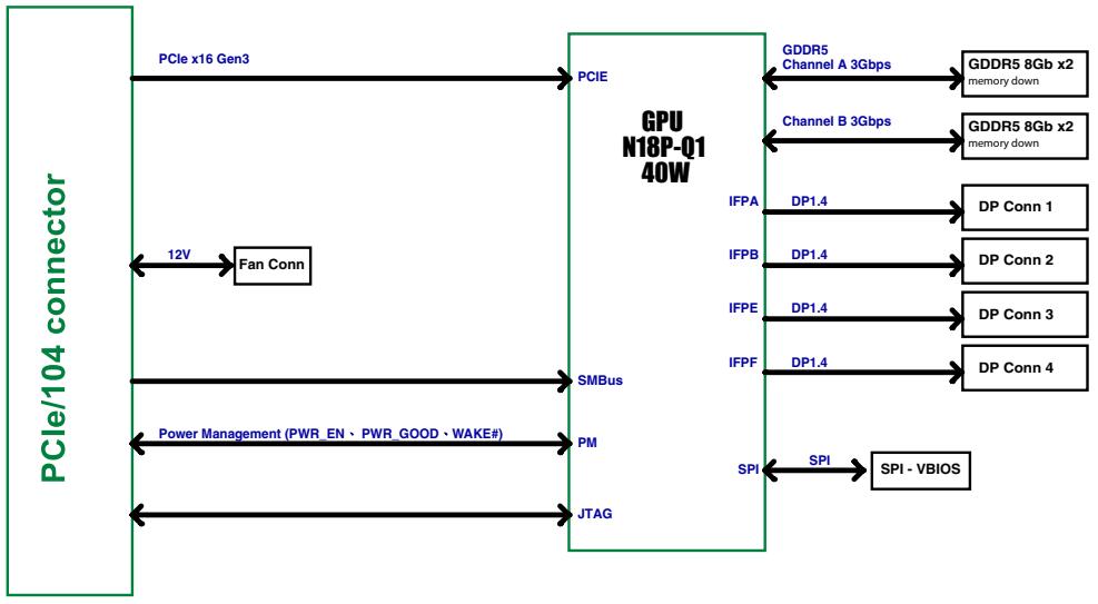
![This block diagram illustrates the connectivity of a **GPU N18P-Q1 40W** module.\n\n**Blocks:**\n*   **PCIe/104 connector** (Left vertical block)\n*   **GPU N18P-Q1 40W** (Center vertical block)\n*   **GDDR5 8Gb x2 memory down** (Two blocks on the top right)\n*   **DP Conn 1**, **DP Conn 2**, **DP Conn 3**, **DP Conn 4** (Four blocks on the middle right)\n*   **Fan Conn** (Small block on the left)\n*   **SPI - VBIOS** (Block on the bottom right)\n\n**Connections:**\n\n*   **PCIe:** From the **PCIe/104 connector** to the **PCIE** input of the GPU. Labeled: **PCIe x16 Gen3**.\n*   **Memory:**\n    *   From the GPU to the top **GDDR5 8Gb x2 memory down** block. Labeled: **GDDR5 Channel A 3Gbps**.\n    *   From the GPU to the bottom **GDDR5 8Gb x2 memory down** block. Labeled: **Channel B 3Gbps**.\n*   **Display Outputs:**\n    *   From the GPU input **IFPA** labeled **DP1.4** to **DP Conn 1**.\n    *   From the GPU input **IFPB** labeled **DP1.4** to **DP Conn 2**.\n    *   From the GPU input **IFPE** labeled **DP1.4** to **DP Conn 3**.\n    *   From the GPU input **IFPF** labeled **DP1.4** to **DP Conn 4**.\n*   **Power/Fan:** From the **PCIe/104 connector** to the **Fan Conn** block. Labeled: **12V**.\n*   **SMBus:** From the **PCIe/104 connector** to the **SMBus** input of the GPU.\n*   **Power Management:** From the **PCIe/104 connector** to the **PM** input of the GPU. Labeled: **Power Management (PWR EN - PWR GOOD - WAKE#)**.\n*   **JTAG:** From the **PCIe/104 connector** to the **JTAG** input of the GPU.\n*   **SPI:** From **SPI - VBIOS** to the **SPI** input of the GPU. Labeled: **SPI**. (Note: The arrow points left towards the GPU).](.cm5-p1000-50m-00052-1000-10/100ddfe5bbe932f8219c39bf3826350b59001fdacb579114402917813fda591b.jpg)

Figure 1-1: CM5-P1000 Functional Block Diagram

# 1.7 Mechanical Dimensions

![The image displays a white sheet of paper with a folded upper-right corner and faint horizontal lines. A large red checkmark is superimposed over the document.](.cm5-p1000-50m-00052-1000-10/ad4cc44cc5064e307211db40f40fe2a283ab787eedf1fc8ed98d87611f0c5b7d.jpg)
NOTE:

All dimensions shown in mm [thou].
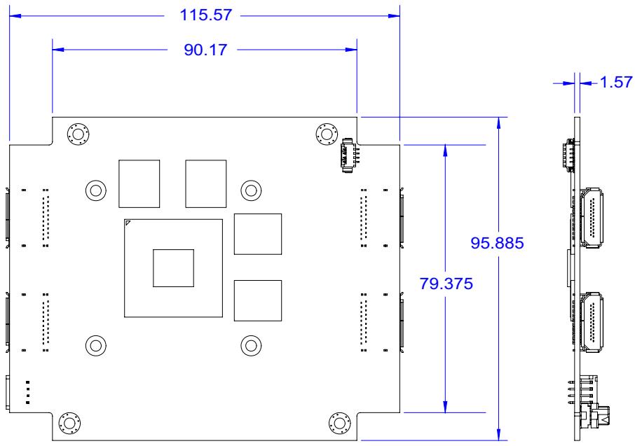
![115.57\n90.17\n1.57\n95.885\n79.375](.cm5-p1000-50m-00052-1000-10/73a2491f4861f89f9d49248c0a07ec72eea97c17a728ef44b994efd9845989c0.jpg)

Figure 1-2: CM5-P1000 Dimensions

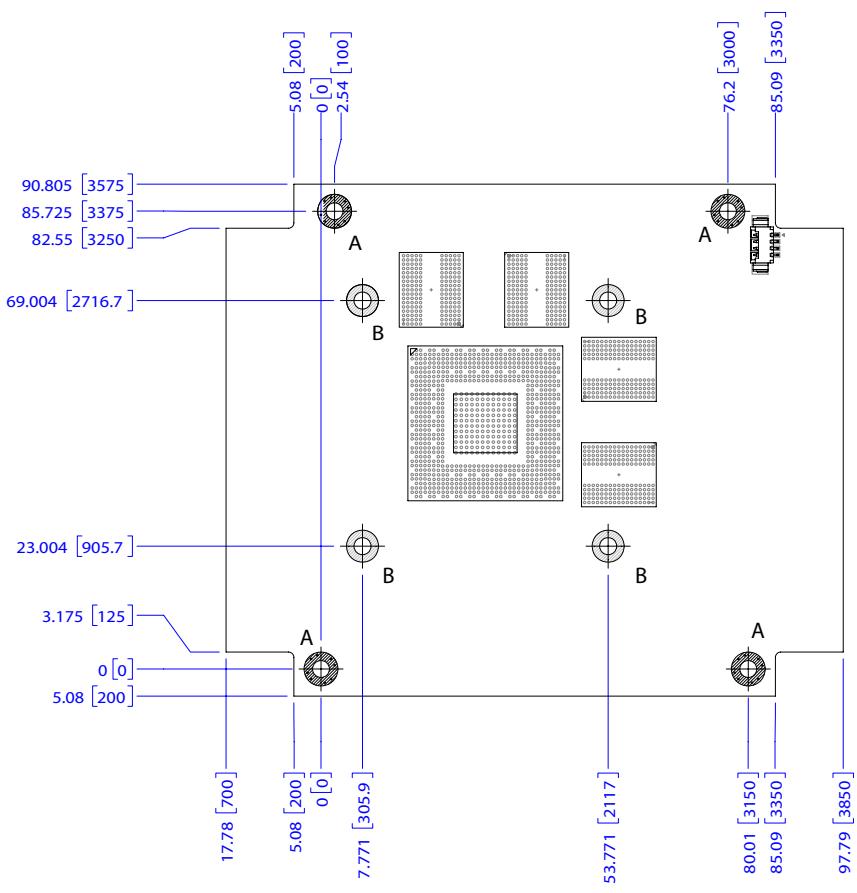
![| Dimension | Value   |\n| --------- | ------- |\n| Total Length | 90.805 |\n| Total Width | 85.725 |\n| Total Height | 82.55 |\n| Total Width (Bottom) | 69.004 |\n| Total Width (Top) | 23.004 |\n| Total Height (Bottom) | 17.78 |\n| Total Width (Top) | 5.08  |\n| Total Width (Bottom) | 5.08  |\n| Total Length (Top) | 7.771 |\n| Total Width (Bottom) | 305.9 |\n| Total Height (Top) | 53.771 |\n| Total Width (Bottom) | 2117 |\n| Total Height (Top) | 80.01 |\n| Total Width (Bottom) | 3150 |\n| Total Height (Top) | 3350 |\n| Total Height (Bottom) | 3850 |\n| Total Thickness | 2.54    |\n| Total Thickness (Top) | 100     |\n| Total Thickness (Bottom) | 700     |\n| Total Thickness (Top) | 3000    |\n| Total Thickness (Bottom) | 200     |\n| Total Thickness (Top) | 3350    |\n| Total Thickness (Bottom) | 3850    |\n| Total Thickness (Top) | 100     |\n| Total Thickness (Bottom) | 200     |\n| Total Thickness (Top) | 5.08    |\n| Total Thickness (Bottom) | 200     |\n| Total Thickness (Top) | 305.9   |\n| Total Thickness (Bottom) | 305.9   |\n| Total Thickness (Top) | 305.9   |\n| Total Thickness (Bottom) | 305.9   |\n| Total Thickness (Top) | 305.9   |\n| Total Thickness (Bottom) | 305.9   |\n| Total Thickness (Top) | 305.9   |\n| Total Thickness (Bottom) | 305.9   |\n| Total Thickness (Top) | 69.004 |\n| Total Thickness (Bottom) | 23.004 |\n| Total Thickness (Top) | 23.004 |\n| Total Thickness (Bottom) | 23.004 |\n| Total Thickness (Top) | 69.004 |\n| Total Thickness (Bottom) | 23.004 |\n| Total Thickness (Top) | 69.004 |\n| Total Thickness (Bottom) | 23.004 |\n| Total Thickness (Top) | 69.004 |\n| Total Thickness (Bottom) | 23.004 |\n| Total Thickness (Top) | 69.004 |\n| Total Thickness (Top) | 23.004 |\n| Total Thickness (Bottom) | 69.004 |\n| Total Thickness (Top) | 69.004 |\n| Total Thickness (Bottom) | 69.004 |\n| Total Thickness (Top) | 69.004 |\n| Total Thickness (Bottom) | 69.004 |\n| Total Thickness (Top) | 69.004 |\n| Total Thickness (Bottom) | 69.004 |\n| Total Thickness (Top) | 69.004 |\n| Total Thickness (Top) | 69.004 |\n| Total Thickness (Bottom) | 69.004 |\n| Total Thickness (Bottom) | 69.004 |\n| Total Thickness (Top) | 69.004 |\n| Total Thickness (Bottom) | 69.004 |\n| Total Thickness (Top) | 69.004 |\n| Total Thickness (Bottom) | 69.004 |\n| Total Thickness (Top) | 69.004 |](.cm5-p1000-50m-00052-1000-10/12089e52833a881817aec992ea575ab69f27769d8acbb685bd27a8b219da55d6.jpg)

Figure 1-3: CM5-P1000 Mounting Specifications
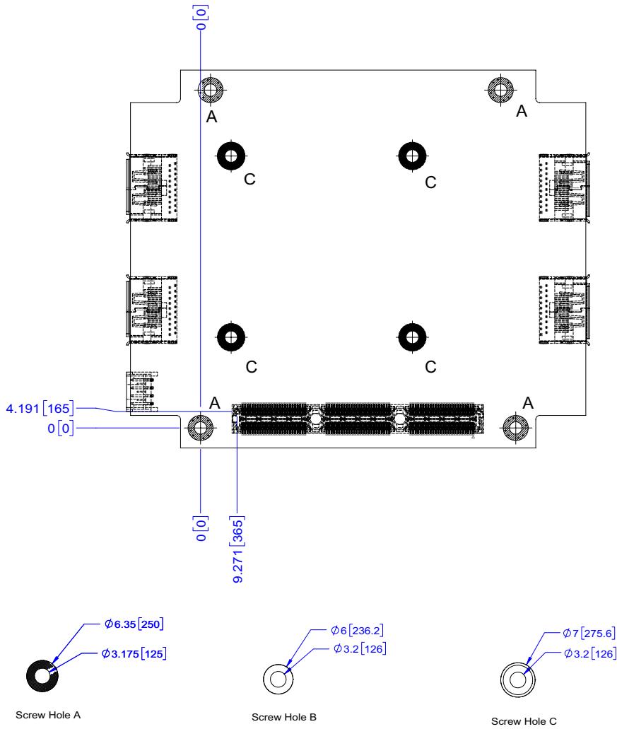
![Screw Hole A\nØ6.35(250)\nØ3.175(125)\nA\nC\nC\nC\nA\n9.271(365)\n4.191(165)\nØ0(0)\nØ6(236.2)\nØ3.2(126)\nScrew Hole B\nØ7(275.6)\nØ3.2(126)\nScrew Hole C](.cm5-p1000-50m-00052-1000-10/47b01d81ecce18395fcbdb39cfd8e1c0b059ff962af641c15f308a9f9b0eb3ad.jpg)

Figure 1-4: CM5-P1000 PCB Specifications

# 1.8 Ordering Information

CM5-P1000-DP
PCIe/104 Type 1 graphics module, NVIDIA Quadro P1000 (640 CUDA cores), 4GB GDDR5, 0°C to +60°C
▶ CM5-P1000-DP-ETT
PCIe/104 Type 1 graphics module, NVIDIA Quadro P1000 (640 CUDA cores), 4GB GDDR5, -40°C to +85°C

For conformal coating please contact your local sales representative.

# 1.9 Unpacking Checklist

Before unpacking, check the shipping carton for any damage. If the shipping carton and/or contents are damaged, inform your dealer immediately. Retain the shipping carton and packing materials for inspection. Obtain authorization from your dealer before returning any product to ADLINK. Ensure that the following items are included in the package.

▶ CM5-P1000 PCIe/104 Graphics Module

# 1.10 Optional Cooling Solutions

The following cooling solutions are available for purchase separately. Please contact your ADLINK representative for detailed more information and mechanical drawings.

# CMx-P1000TM-00

CM5-P1000 heat spreader, -40°C to 85°C (P/N: 91-95291-100E)
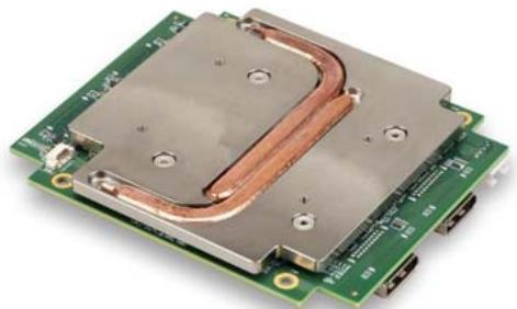
![Close-up of a green circuit board with a copper-colored heat sink component (no visible text or symbols)](.cm5-p1000-50m-00052-1000-10/231e44f0d3a95e840661eec5b4eb9a44f13ce49430dd69ee49faefb39ef0fc2c.jpg)

# CMx-P1000TM-10

CM5-P1000 passive heat sink, -40°C to 85°C with air flow (P/N: 91-95291-200E)
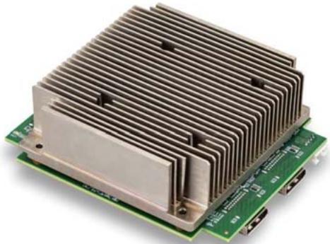
![Close-up of a heat sink cooling system mounted on a green circuit board (no text or symbols visible)](.cm5-p1000-50m-00052-1000-10/2b722101115f9b6fa3e029cbbc9cfeb6abbfe9600c005200417388683f9228be.jpg)

# CMx-P1000TM-20

CM5-P1000 active heat sink, -10°C to 70°C (P/N: 91-95291-300E)
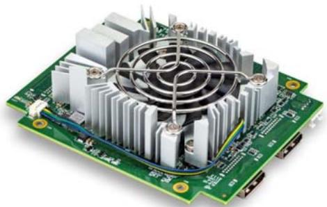
![Close-up of a green printed circuit board with a central fan and cooling elements (no visible text or symbols)](.cm5-p1000-50m-00052-1000-10/fa1f12c7afb6897b5f07b4ee71abab81d000f53d9418ccc133c97dab017d4db9.jpg)

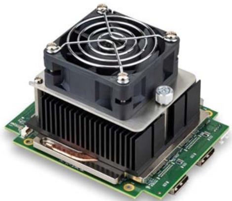
# CMx-P1000TM-30

CM5-P1000 active heat sink (for ETT testing only, requires external 4-pin Molex power), -40°C to 85°C (P/N: 91-95291-400E)
![Close-up of a black CPU cooling fan mounted on a green circuit board (no visible text or symbols)](.cm5-p1000-50m-00052-1000-10/f032542795242e95e04563246a22c9deffc85915928b6d48eb29d97c77560c81.jpg)

# 2 Interfaces

# 2.1 Board Layout

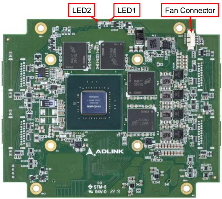
![LED2\nLED1\nFan Connector\nADLINK\nSTM-5\n94V-0 22:3](.cm5-p1000-50m-00052-1000-10/55b24dc71f11b711a42fa633cc6f604ee1839de17408e0de1cde2f198663cc6a.jpg)

Figure 2-1: CM5-P1000 Top Side Layout

<table><tr><td>LED1</td><td>Power on LED</td></tr><tr><td>LED2</td><td>Over-temperature LED</td></tr></table>

![DP 3\nDP 1\nPCIe/104 Connector\nDP 2\nDP 4\nExternal DC Input](.cm5-p1000-50m-00052-1000-10/879968e310758d98be2c94cb924fca0b54e4f47bcf555a3a339ae764a1c56f10.jpg)

Figure 2-2: CM5-P1000 Bottom Side Layout

# 2.2 Connectors

Fan Connector (1.25mm pitch wafer)

<table><tr><td>Pin</td><td>Signal</td></tr><tr><td>1</td><td>FAN_ON</td></tr><tr><td>2</td><td>FAN_TACH</td></tr><tr><td>3</td><td>12V</td></tr><tr><td>4</td><td>GND</td></tr></table>

![Close-up of a green printed circuit board with a white connector and connectors (no readable text or symbols)](.cm5-p1000-50m-00052-1000-10/a3ed8a87585096c272ae140d8f19ae97775813e161d0977152faf1f25fcb65b7.jpg)

External DC Input (2.00mm pitch wafer)

<table><tr><td>Pin</td><td>Signal</td></tr><tr><td>1</td><td>12V*</td></tr><tr><td>2</td><td>12V*</td></tr><tr><td>3</td><td>GND</td></tr><tr><td>4</td><td>GND</td></tr></table>

![Close-up of a green circuit board with visible connectors and a labeled component 'CON301' (no other text or symbols)](.cm5-p1000-50m-00052-1000-10/7dcbb745db4689370fc8d97dd18865282ecd7d1ea9d43d3242cae7b2fafc12a6.jpg)

![This image displays a digital icon of a white document or sheet of paper with a folded top-right corner. Faint grey horizontal lines run across the paper, suggesting text or a list. A large, bold red checkmark is drawn diagonally across the center of the document.](.cm5-p1000-50m-00052-1000-10/46e2b0083ba8a3f756aae22559ef40e38ba807d71bb93225d36c2e15abfb1c14.jpg)
NOTE:

Use the same power source as "+12V" of the PCIe104 connector

DisplayPort Connectors

<table><tr><td>Pin</td><td>Signal</td></tr><tr><td>1</td><td>IFPA_L0_C_P</td></tr><tr><td>2</td><td>GND</td></tr><tr><td>3</td><td>IFPA_L0_C_N</td></tr><tr><td>4</td><td>IFPA_L1_C_P</td></tr><tr><td>5</td><td>GND</td></tr><tr><td>6</td><td>IFPA_L1_C_N</td></tr><tr><td>7</td><td>IFPA_L2_C_P</td></tr><tr><td>8</td><td>GND</td></tr><tr><td>9</td><td>IFPA_L2_C_N</td></tr><tr><td>10</td><td>IFPA_L3_C_P</td></tr><tr><td>11</td><td>GND</td></tr><tr><td>12</td><td>IFPA_L3_C_N</td></tr><tr><td>13</td><td>IFPA_AUX_SEL</td></tr><tr><td>14</td><td>DP_A_CFG2</td></tr><tr><td>15</td><td>IFPA_AUX_C_P</td></tr><tr><td>16</td><td>GND</td></tr><tr><td>17</td><td>IFPA_AUX_C_N</td></tr><tr><td>18</td><td>IFPA_HPD</td></tr><tr><td>19</td><td>GND</td></tr><tr><td>20</td><td>P_+3V3</td></tr><tr><td>21</td><td>CHA_GND</td></tr><tr><td>22</td><td>CHA_GND</td></tr><tr><td>23</td><td>CHA_GND</td></tr><tr><td>24</td><td>CHA_GND</td></tr></table>

![1\n2\n19\n20](.cm5-p1000-50m-00052-1000-10/9484da20b92a408607abbe1243f5fbfc535a3de308c14cb9658479d8a5a2c0ba.jpg)

# 3 System Requirements

# 3.1 Power Sequencing

For initial power on, or to Resume from S3 and S4, this sequence must be followed.

![| Category           | Value |\n| ------------------ | ----- |\n| PWR_SRC            | T_PV-PE |\n| 5V                 | T_PV-PE |\n| 3V3                | T_PV-PE |\n| PWR_EN             | T_PV-PE |\n| Module Internal Power | T_PE-PG |\n| PWR_GOOD           | T_PE-PG |\n| Total Time         | T_PV-PE ≥0ms |\n| Total Time         | T_PE-PG ≤90ms |](.cm5-p1000-50m-00052-1000-10/e6134de1eb9dcc6113e71ddd6c75289a753b8476baa38f8c9964a4d04810d219.jpg)

Figure 3-1: Power Sequencing

# 3.2 Module Power Up and Down

Issuing the PWR\_EN signal powers the CM5-P1000 module down, and the system designer can decide whether to keep the module input power when the CM5-P1000 module is powered down.

![MODULE\nINPUT POWER\nPWR_EN\nMODULE\nINTERNAL POWER\nPWR_GOOD](.cm5-p1000-50m-00052-1000-10/89119c2504e0d9b365194a383c94430cafcc7302b8d6bed5a71329f616ff0330.jpg)

Figure 3-2: Module Power Down

# 3.3 Reset Requirements

![| Signal          | Value     |\n|-----------------|-----------|\n| MODULE INPUT POWER | T_PVPERL  |\n| PWR_EN          | T_PVPERL  |\n| PWR_GOOD        | T_PVPERL  |\n| PEX_REFCLK      | T_PVPERL  |\n| PEX_RST#        | T_PVPERL  |\n| T_PVERST-PG     | T_PERST-PG |\n| T_PERST-CLK     | T_PERST-CLK |\n| T_FAIL          | T_PERST-CLK |\n| T_PVPERL ≥100 ms | T_PVPERL  |\n| T_PERST-CLK ≥100 μs | T_PERST-CLK |\n| T_PERST-PG ≥200 μs | T_PERST-PG |\n| T_FAIL ≤ 500 ns  | T_PERST-CLK |](.cm5-p1000-50m-00052-1000-10/ee57cfe4864484da279b43db1899e1d287016a96da4f1cf8f57b7b9e2b23cc80.jpg)

Figure 3-3: Reset Sequencing

# 3.4 Thermal Policy

The GPU core clock throttles at temperatures ( $T_{J}$ ) past the thresholds shown with the behaviors as listed. Thermal throttling ensures that the highest temperature on the die does not exceed the sense temperature for prolonged periods of time.

<table><tr><td>Parameter</td><td>Value</td><td>Unit</td></tr><tr><td>Thermal Resistance (Junction to Case,  $R_{JC}$ )</td><td>0.03</td><td>°C/W</td></tr><tr><td>Thermal Resistance (Junction to PCB Board,  $R_{JB}$ )</td><td>3.0</td><td>°C/W</td></tr><tr><td>GPU Maximum Operating Temperature $^{1}$ </td><td>94</td><td>°C</td></tr><tr><td>GPU Slowdown Temperature (THERM_ALERT) $^{2}$ </td><td>97</td><td>°C</td></tr><tr><td>GPU Shutdown Temperature (OVERT) $^{3}$ </td><td>102</td><td>°C</td></tr></table>

Table 3-1: Thermal Policy

![This image displays a simple icon of a white document with faint horizontal gray lines and a folded top-right corner, overlaid with a large red checkmark.](.cm5-p1000-50m-00052-1000-10/32876f1223ea4c4424278b6436b06059ae8c8da353f485f4569ebf12b7858af6.jpg)
NOTE:

$^{1}$ Max.GPU operating temperature is the maximum at which the GPU is guaranteed to operate at target performance (base clock) under total board power level
$^{2}$ THERM\_ALERT generates a 50% (÷2) hardware clock slowdown.
$^{3}$ OVERT generates a 87.5% (÷8) hardware clock slowdown

# 3.5 BIOS Settings

When the CM5-P1000 is used with the ADLINK CM4-SL2 PCI/104-Express SBC, please use the following BIOS settings to ensure proper graphics functionality.

1. Advanced > Graphics > Primary Display: set to PCIE
2. Boot > CSM > Video: set to UEFI
3. Boot > CSM > CSM Support: set to Disabled

For detailed information about the ADLINK CM4-SL2's BIOS settings, please refer to the CMx-SLx Technical Reference, Section 4.1 BIOS Setup, downloadable from the ADLINK website.

For BIOS setting information when used with other PCI/104-Express or PCIe/104 SBCs, please consult the manufacturer's documentation.

# 3.6 Driver Installation

Drivers can be downloaded from https://www.adlinktech.com/Products/PC104SBCs/PCIe104/CM5-P1000.

# 3.7 Certifications & Agencies

▶ Windows Hardware Quality Lab (WHQL) certified Windows 7, and Windows 10
▶ EU Reduction of Hazardous Substances (EU-RoHS)
▶ Conformité Européenne (CE)
▶ Federal Communications Commission (FCC)

# Important Safety Instructions

For user safety, please read and follow all instructions, Warnings, Cautions, and Notes marked in this manual and on the associated device before handling/operating the device, to avoid injury or damage.

S'il vous plaît prêter attention stricte à tous les avertissements et mises en garde figurant sur l'appareil, pour éviter des blessures ou des dommages.

▶ Read these safety instructions carefully
- Keep the User’s Manual for future reference
▶ Read the Specifications section of this manual for detailed information on the recommended operating environment
▶ The device can be operated at an ambient temperature of $50^{\circ}$ C
- When installing/mounting or uninstalling/removing device; or when removal of a chassis cover is required for user servicing:
▷ Turn off power and unplug any power cords/cables
▶ Reinstall all chassis covers before restoring power
▶ To avoid electrical shock and/or damage to device:
▷ Keep device away from water or liquid sources
▷ Keep device away from high heat or humidity
▷ Keep device properly ventilated (do not block or cover ventilation openings)
▶ Always use recommended voltage and power source settings
▶ Always install and operate device near an easily accessible electrical outlet
▷ Secure the power cord (do not place any object on/over the power cord)
▷ Only install/attach and operate device on stable surfaces and/or recommended mountings

▶ If the device will not be used for long periods of time, turn off and unplug from its power source

▶ Never attempt to repair the device, which should only be serviced by qualified technical personnel using suitable tools

▶ A Lithium-type battery may be provided for uninterrupted backup or emergency power.

![The image displays a yellow triangular warning sign with a black border. Inside the triangle is a black exclamation point. Below the triangle, the text 'CAUTION:' is printed in black capital letters.](.cm5-p1000-50m-00052-1000-10/cf0dab3f305df29b4587dc00bd38a6a7de4eaade65f9fa5303a5e68ca93c325b.jpg)

Risk of explosion if battery is replaced with one of an incorrect type; please dispose of used batteries appropriately.

Risque d'explosion si la pile est remplacée par une autre de type incorrect. Veuillez jeter les piles usagées de façon appropriée.

▶ The device must be serviced by authorized technicians when:

The power cord or plug is damaged
▷ Liquid has entered the device interior
The device has been exposed to high humidity and/or moisture
The device is not functioning or does not function according to the User's Manual
The device has been dropped and/or damaged and/or shows obvious signs of breakage

▶ Disconnect the power supply cord before loosening the thumbscrews and always fasten the thumbscrews with a screwdriver before starting the system up

It is recommended that the device be installed only in a computer room where access is:

▶ Restricted to qualified service personnel or users familiar with restrictions applied to the location, reasons therefor, and any precautions required

▶ Only afforded by the use of a tool or lock and key, or other means of security, and controlled by the authority responsible for the location

![Yellow triangular warning sign with black smoke symbol indicating hot weather](.cm5-p1000-50m-00052-1000-10/d4c8b7a44c7b06581dc23db259149d2245bda5af4a0c0f0a2a4786fdc378e198.jpg)

# BURN HAZARD

Touching this surface could result in bodily injury. To reduce risk, allow the surface to cool before touching.

# RISQUE DE BRÛLURES

Ne touchez pas cette surface, cela pourrait entraîner des blessures.

Pour éviter tout danger, laissez la surface refroidir avant de la toucher.

This page intentionally left blank.

# Getting Service

Ask an Expert: http://askanexpert.adlinktech.com

# ADLINK Technology, Inc.

No. 66, Huaya 1st Rd., Guishan Dist.,

Taoyuan City 333411, Taiwan

Tel: +886-3-216-5088

Fax: +886-3-328-5706

Email: service@adlinktech.com

# Ampro ADLINK Technology, Inc.

6450 Via Del Oro

San Jose, CA 95119-1208, USA

Tel: +1-408-360-0200

Toll Free: +1-800-966-5200 (USA only)

Fax: +1-408-600-1189

Email: info@adlinktech.com

# ADLINK Technology (China) Co., Ltd.

300 Fang Chun Rd., Zhangjiang Hi-Tech Park

Pudong New Area, Shanghai, 201203 China

Tel: +86-21-5132-8988

Fax: +86-21-5132-3588

Email: market@adlinktech.com

# ADLINK Technology GmbH

Hans-Thoma-Strasse 11

D-68163 Mannheim, Germany

Tel: +49-621-43214-0

Fax: +49-621 43214-30

Email: emea@adlinktech.com

Please visit the Contact page at www.adlinktech.com for information on how to contact the ADLINK regional office nearest you:
[🔗 Link to the original document](.cm5-p1000-50m-00052-1000-10/cm5-p1000-50m-00052-1000-10.pdf)