# CMx-BTx

# Technical Manual

PC/104-based Single Board Computer with Intel Atom® E3800 Series Processors

![Close-up of a green printed circuit board with various electronic components and connectors (no readable text or symbols)](.cmx-btx-50m-95186-5000-50/f6b608518b86c3d9d57a60cf1c074aa098fb01f6bb0eb318be989e3f6d1ea7e4.jpg)

Manual Rev.: 5.0

Revision Date: January 7, 2025

Part Number: 50M-95186-5000

# Preface

# Disclaimer

Information in this document is provided in connection with ADLINK products. No license, express or implied, by estoppel or otherwise, to any intellectual property rights is granted by this document. Except as provided in ADLINK´s Terms and Conditions of Sale for such products, ADLINK assumes no liability whatsoever, and ADLINK disclaims any express or implied warranty, relating to sale and/or use of ADLINK products including liability or warranties relating to fitness for a particular purpose, merchantability, or infringement of any patent, copyright or other intellectual property right. If you intend to use ADLINK products in or as medical devices, you are solely responsible for all required regulatory compliance, including, without limitation, Title 21 of the CFR (US), Directive 2007/47/EC (EU), and ISO 13485 & 14971, if any. ADLINK may make changes to specifications and product descriptions at any time, without notice.

# Trademarks

Product names mentioned herein are used for identification purposes only and may be trademarks and/or registered trademarks of their respective companies.

Revision History

<table><tr><td>Revision</td><td>Reason for Change</td><td>Date</td></tr><tr><td>1.0</td><td>Initial Release</td><td>2015-05-08</td></tr><tr><td>2.0</td><td>Revised for new board layout</td><td>2015-08-27</td></tr><tr><td>3.0</td><td>Revised for new revision of the board; removed USB 3.0 functionality and added BAT1 interface</td><td>2016-02-12</td></tr><tr><td>4.0</td><td>Added note to Section 4.4.8, requiring a connected RTC battery for enabled ECO mode</td><td>2016-08-08</td></tr><tr><td>4.1</td><td>Added heat spreader installation procedure to Section 2.4; added requirements for SODIMM installation to Table 1-1; Updated BIOS setup section to new format and content in Chapter 4; updated Figure 2-2 to change CN17 from 10 to 9 pins; revised P/N of CN17 mating connector in Table 2-2; Added PM changes from review of rev 5.02; Removed SATA cable from cable set in Table 2-1</td><td>2017-11-16</td></tr><tr><td>4.2</td><td>Updated BMC exception blink codes in Table 4-2; moved BIOS Setup section to its own chapter; moved System Resources to their own chapter</td><td>2018-10-31</td></tr><tr><td>4.3</td><td>Remove description of unsupported RS485 functionality, add HD Audio (CN15) description</td><td>2020-11-16</td></tr><tr><td>4.4</td><td>Add French safety warnings</td><td>2021-02-04</td></tr><tr><td>4.5</td><td>Update support OS, BIOS info</td><td>2022-07-27</td></tr><tr><td>4.6</td><td>Update specifications, On-Board Power Supply description</td><td>2023-06-28</td></tr><tr><td>5.0</td><td>Revised for updated PCB</td><td>2025-01-07</td></tr></table>

Copyright © 2015, 2016, 2017, 2018, 2020, 2021, 2022, 2023, 2025 ADLINK Technology, Inc.

www.adlinktech.com

This document contains proprietary information protected by copyright. All rights are reserved. No part of this manual may be reproduced by any mechanical, electronic, or other means in any form without prior written permission of the manufacturer.

# Audience

This manual provides reference only for computer design engineers, including but not limited to hardware and software designers and applications engineers. ADLINK Technology, Inc. assumes you are qualified to design and implement prototype computer equipment.

# Environmental Responsibility

ADLINK is committed to fulfill its social responsibility to global environmental preservation through compliance with the European Union's Restriction of Hazardous Substances (RoHS) directive and Waste Electrical and Electronic Equipment (WEEE) directive. Environmental protection is a top priority for ADLINK. We have enforced measures to ensure that our products, manufacturing processes, components, and raw materials have as little impact on the environment as possible. When products are at their end of life, our customers are encouraged to dispose of them in accordance with the product disposal and/or recovery programs prescribed by their nation or company.

![Symbol of a trash bin crossed with a diagonal line and a horizontal bar below (no text or labels)](.cmx-btx-50m-95186-5000-50/3800d6cc10c55b425bed4734f6c4d9a15959c097328891baece035fb599a2853.jpg)

Battery Labels (for products with battery)

![Symbol of a trash bin crossed out by two diagonal lines (no text or labels)](.cmx-btx-50m-95186-5000-50/2aa5fe404adaf63f8ea1d79cd79d8288e08b54c72e41f8f5095e99a39c77125f.jpg)

![The image displays a black outline of a square containing the universal recycling symbol. Inside the square, three black arrows are arranged in a triangular formation, with each arrow pointing clockwise towards the next, set against a white background.](.cmx-btx-50m-95186-5000-50/f8bad62ec5ff7b2c3988cd6d4c8933d7de84480dfb32435c77db5b9f298e4ea1.jpg)
Li-ion

![RECYCLE\nRBRC\nLi-ion\n7.800.822.8837](.cmx-btx-50m-95186-5000-50/4eeaecfef43980cf8a55f213533bad720107f66ecd8a12abb84c8ed146c77f30.jpg)

![The image displays a black and white QR code. It features three large square finder patterns located in the top-left, top-right, and bottom-left corners. The remaining area is occupied by a grid of smaller black and white squares representing data modules.](.cmx-btx-50m-95186-5000-50/ec4c6e42292155d2544cfa74316218cec7c543b77c3e956a8fce26fdab11ddbf.jpg)
ᑜ㔚ᳰ⺧࿁ᡴ

# California Proposition 65 Warning

![The image features a yellow triangular warning sign with a thick black border. Centered inside the triangle is a black exclamation mark. The background is white.](.cmx-btx-50m-95186-5000-50/331376dfcd5829851c9b09449d596766553900db4df373c13a0921ecd6b42e0f.jpg)

WARNING: This product can expose you to chemicals including acrylamide, arsenic, benzene, cadmium, Tris(1,3-dichloro-2-propyl)phosphate (TDCPP), 1,4-Dioxane, formaldehyde, lead, DEHP, styrene, DINP, BBP, PVC, and vinyl materials, which are known to the State of California to cause cancer, and acrylamide, benzene, cadmium, lead, mercury, phthalates, toluene, DEHP, DIDP, DnHP, DBP, BBP, PVC, and vinyl materials, which are known to the State of California to cause birth defects or other reproductive harm. For more information go to www.P65Warnings.ca.gov.

AVERTISSEMENT: Ce produit peut vous exposer à des produits chimiques tels que l'acrylamide, l'arsenic, le benzène, le cadmium, le phosphate de tris (1,3-dichloro-2-propyle) (TDCPP), le 1,4-dioxane, le formaldéhyde, le plomb, le DEHP, le styrène, le DINP , BBP, PVC et matériaux en vinyle, qui sont connus dans l'État de Californie pour causer le cancer, et acrylamide, benzène, cadmium, plomb, mercure, phtalates, toluène, DEHP, DIDP, DnHP, DBP, BBP, PVC et vinyle matériaux, qui sont connus de l'État de Californie pour causer des anomalies congénitales ou d'autres troubles de la reproduction. Pour plus d'informations, visitez le site www.P65Warnings.ca.gov.

# Conventions

The following conventions may be used throughout this manual, denoting special levels of information.

![The image displays a vertical icon. The top portion features a white document graphic with a folded upper-right corner and faint horizontal lines. A large, bold red checkmark is centered on the document. Below the graphic, the text 'NOTE:' is written in black capital letters.](.cmx-btx-50m-95186-5000-50/6f81cade91d00273a63ec011abd77da3e90e0e2729fd81dcc3420a3690188b6c.jpg)

This information adds clarity or specifics to text and illustrations.

![The image displays a bilingual warning sign. At the top is a yellow triangle with a black border containing a black exclamation point. Below the symbol, the text reads 'CAUTION:' in black capital letters, followed by the phrase 'MISE EN GARDE' in black capital letters on the line below.](.cmx-btx-50m-95186-5000-50/d64a16d8c0cf2717da0aa69a379b0ce5e9d4a663ae4146e1e0b1c5e568edb69b.jpg)

This information indicates the possibility of minor physical injury, component damage, data loss, and/or program corruption.

Ces informations indiquent la possibilité de blessures physiques mineures, de dommages aux composants, de perte de données et / ou de corruption de programme.

![The image displays a vertical warning sign. At the top is a red triangle with a white exclamation mark in the center. Below the symbol, the text reads 'WARNING:' in bold black capital letters, followed by 'ATTENTION' in black capital letters where the letter 'A' is slightly larger than the rest.](.cmx-btx-50m-95186-5000-50/1af644c794c928eb32407f7ba2f3057cedbae9898eb1091efe7e89cd25a4d5d7.jpg)

This information warns of possible serious physical injury, component damage, data loss, and/or program corruption.

Ces informations mettent en garde contre d'éventuelles blessures physiques graves, des dommages aux composants, une perte de données et / ou une corruption du programme.

# Important Safety Instructions

For user safety, please read and follow all Instructions, WARNINGs, CAUTIONs, and NOTEs marked in this manual and on the associated equipment before handling/operating the equipment.

 Read these safety instructions carefully.
 Keep this manual for future reference.
 Read the specifications section of this manual for detailed information on the operating environment of this equipment.
 Turn off power and unplug any power cords/cables when installing/mounting or un-installing/removing equipment.
 To avoid electrical shock and/or damage to equipment:

 Keep equipment away from water or liquid sources;
 Keep equipment away from high heat or high humidity;
 Keep equipment properly ventilated (do not block or cover ventilation openings);
 Make sure to use recommended voltage and power source settings;
 Always install and operate equipment near an easily accessible electrical socketoutlet;
 Secure the power cord (do not place any object on/over the power cord);
 Only install/attach and operate equipment on stable surfaces and/or recommended mountings; and,
 If the equipment will not be used for long periods of time, turn off the power source and unplug the equipment.

# Table of Contents

# Preface . ii

# 1 Introduction.....

1.1 Overview.. 1
1.2 Features...
1.3 Block Diagram.. ..2
1.4 Ordering Information .. ..3
1.5 Specifications... .4

1.5.1 Electrical Specifications . 4
1.5.2 Environmental Specifications...... .4
1.5.3 Mechanical Specifications . .5
1.5.4 Heat Sink Specifications . .5

# 2 Getting Started..

2.1 Header and Connector Locations .........
2.2 Mechanical Dimensions........ ..11
2.3 LED Indicators .. . 12
2.4 Hardware Setup ........... .... 13
2.5 Windows 10 Installation . .. 15

# 3 Module Description .... ... 17

3.1 SoC (System on a Chip) .. . 17

3.1.1 Processor Core... . 17
3.1.2 Memory Controller .. . 17
3.1.3 Graphics Engine . .17
3.1.4 Image Signal Processor.. .. 18
3.1.5 Power Management.. .. 18
3.1.6 PCI Express ...... .... 18
3.1.7 SATA Controller ....... ... 18
3.1.8 USB xHCI Controller.. .. 18
3.1.9 USB 2.0 EHCI Controller ..... ....18
3.1.10 HD-Audio Controller...... .... 18
3.1.11 Intel® Trusted Execution Engine (Intel® TXE) .. .. 19
3.1.12 Platform Control Unit (PCU) . 19

3.2 VGA Interface ......... ..... 19
3.3 LVDS Interface......... .. 20
3.4 LVDS Backlight.. .. 21

3.4.1 Selecting Panel and Backlight voltage.. . 22

3.5 Ethernet Controllers .. .. 23
3.6 USB Ports .. .. 25
3.7 On-Board Power Supply ... ..26
3.8 System Panel... .. 27
3.9 Serial Ports ........ ..28

3.10 Setting RS422 Termination . . 30
3.11 Mini-PCIe Interface .... . 31
3.12 PCI-104 Bus Interface.. . 32
3.13 PC/104 Bus Interface .. . 34
3.14 Audio Interface . . 36
3.15 BMC Service Connector.. . 37
3.16 User GPIO Interface.. . 39
3.17 Fan Interface ... . 40
3.18 Battery Interface .. . 40

# 4 Using the Module .. . 41

4.1 SEMA Functions . . 41

4.1.1 Board Specific SEMA Functions ... . 42
4.1.2 Watchdog Timer... . 43

4.2 SW4 BIOS Control Switch.. . 44
4.3 Temperature Sensors . .. 45
4.4 Real Time Clock (RTC) . 45

# 5 BIOS Setup . . 47

5.1 Menu Structure.... .. 47
5.2 Starting the BIOS Setup Utility .. . 48
5.3 Main Menu .......... ..... 48

5.3.1 Main > BIOS Information.. . 48
5.3.2 Main > CPU Information.. . 48
5.3.3 Main > Memory Information .. . 48
5.3.4 Main > VGA Information.. . 48
5.3.5 Main > TXE Information ... . 49
5.3.6 Main > System Management . 49
5.3.7 Main > System Management > Temperatures and Fan Speed . . 49
5.3.8 Main > System Management > Power Consumption.. . 50
5.3.9 Main > System Management > Runtime Statistics . . 50
5.3.10 Main > System Management > Flags ....... . 51
5.3.11 Main > System Management > Power Up .. . 51
5.3.12 Main > System Management > LVDS Backlight . . 52
5.3.13 Main > System Management > Smart Fan ...... . 52
5.3.14 Main > System Date and Time.......... . 53

5.4 Advanced Menu ......... . 53

5.4.1 Advanced > CPU Configuration . . 53
5.4.2 Advanced > Graphics Configuration .. . 54
5.4.3 Advanced > SATA Configuration .. . 55
5.4.4 Advanced > USB Configuration . . 56
5.4.5 Advanced > SDIO Configuration.. . 57
5.4.6 Advanced > Network Configuration.. . 57
5.4.7 Advanced > Audio Configuration . . 57
5.4.8 Advanced > PCI and PCIe Configuration.. . 58

5.4.9 Advanced > PCI and PCIe > PCIe Configuration Settings . . 59

5.4.10 Advanced > PCI and PCIe > PCI Subsystem Settings. .. 60

5.4.11 Advanced > Baytrail Features Configuration . .. 61

5.4.12 Advanced > ACPI Settings . .. 61

5.4.13 Advanced > Serial Port Console Redirection.. . 62

5.4.14 Advanced > Thermal Configuration . .62

5.4.15 Advanced > Security Configuration .. . 63

5.4.16 Advanced > Miscellaneous.. . 63

5.4.17 Advanced > NCT5104D Super IO Configuration.. . 64

5.4.18 Advanced > Ethernet Controls. .. 66

5.4.19 Advanced > Mini-PCIe-Slot function. . 66

5.4.20 Advanced > USB Controls . 66

5.5 Boot Menu.... ... 67

5.5.1 Boot > Boot Configuration.. . 67

5.5.2 Boot > Boot Configuration > CSM Configuration .. .. 68

5.6 Security Menu.. .. 68

5.7 Save & Exit Menu . .. 69

# 6 System Resources ... . 71

6.1 Memory Address Map.. ..71

6.2 I/O Address Map.. .. 74

6.3 PCI Configuration Registers ..75

6.4 IO Register Maps.. .. 77

6.4.1 CMOS Memory and RTC Registers . . 77

6.5 Interrupts.. .. 78

6.5.1 SERIRQ Interrupt Mapping. .. 78

# 7 Getting Service ...... . 79

This page intentionally left blank.

# 1 Introduction

# 1.1 Overview

The CMx-BTx is a PC/104-based, Single Board Computer (SBC), fully compliant with the PCI-104 Specification, Version 1.1 and partially compliant with the PC/104 Specification, Version 2.6. PC/104 SBCs are very compact and highly integrated computers. This SBC features the 22nm Intel® Bay Trail SoC.

The board provides a DDR3L SODIMM socket, a PC/104 connector and/or a PCI-104 connector, up to four USB 2.0 ports (with one port routed to mini-PCIe slot), up to two Gigabit Ethernet ports, up to two SATA 3 Gb/s ports, one dedicated HD-Audio panel connector, one VGA port, one LVDS port, up to four COM ports, one mini-PCIe slot (shared with one USB 2.0 port).

The CMx-BTx can be run with only 5 volts and is capable of running operating systems like DOS, Windows 7/8.1/10 in either 32-bit or 64-bit configuration, Linux, VxWorks, and others.

Another feature included on the board is a secondary BIOS that enables the user to start the module even if the original BIOS is corrupted (see “SW4 BIOS Control Switch” on page 44).

# 1.2 Features

<table><tr><td rowspan="2">SoC► Intel® Bay Trail I/M/D with integrated Graphics► Bay Trail-I Premium (E3845)► Bay Trail-I Med (E3825)► Bay Trail-I Entry (E3815)</td><td>Main Memory► Single channel 64bit 1067 MT/s and 1333 MT/s Non-ECC, unbuffered DDR3L SODIMM up to 4 GB</td></tr><tr><td>Expansion slots► 1x mini-PCIe with mSATA and USB capability (3.3V I/O)► 1x 16-bit PC/104 without DMA and no bus mastering capability► 1x 32-bit PCI-104</td></tr><tr><td>Interfaces► 2x Ethernet, 1GBit► 2x SATA 3Gb/s► 4x USB 2.0 (one routed to mini-PCIe slot)► 4x RS232/422► 5.1 channel HD-Audio (analog &amp; SPDIF)► 1x VGA</td><td>► 1x 18/24 Bit LVDS for displays► 8x User GPIO► System panel connector for power and reset button cable, watchdog out, speaker and HDD-LED</td></tr></table>

![The image displays a white document icon featuring a large red checkmark and faint horizontal lines representing text. Below the icon, the word 'NOTE:' is written in black capital letters.](.cmx-btx-50m-95186-5000-50/a35bdb371c21bcdd85e47e9d652538a058156b3303b0de86e3cd5dfefa8e2fc9.jpg)

Other configurations are possible. Please contact your local ADLINK Technology representative to discuss requirements.

# 1.3 Block Diagram

![Based on the provided block diagram, here are the labeled blocks and their connections:\n\n**Central Component**\n*   **CMx-BTx** (Title)\n*   **Intel BayTrail-I SoC**\n    *   E3845 (4C)\n    *   E3825 (2C)\n    *   E3815 (1C)\n\n**Left Side Blocks & Connections**\n*   **VGA** (Connected directly to SoC)\n*   **LVDS single/dual channel 18/24 bit** (Connected via **PTN3460 eDP to LVDS**, labeled **D01.0 (eDP 1.1/2 wire)**)\n*   **Inverter (Backlight)** (Connected via **LVDS Inverter CTRL**)\n*   **Micro SD socket** (Connected via **SDIO**)\n*   **HD Audio** (Connected via **ALC888 Audio Codec**)\n*   **1st GbE** (Connected via **I210IT Ethernet**, labeled **PCIe(0)x1**)\n*   **Optional: 2nd GbE** (Connected via **I210IT Ethernet (option)**, labeled **PCIe(1)x1**)\n*   **PCI-104** (Connected via **XIO2001 IZA PCIe to PCI**, labeled **PCIe(2)x1**)\n*   **Optional: PC/104** (Connected via **F85226AD-I LPC to ISA (option)**, labeled **LPC**)\n\n**Right Side Blocks & Connections**\n*   **DDR3L-1333 SO-DIMM socket** (Connected via **Channel 0**)\n*   **1x USB 2.0** (Connected to SoC; also connects to the **mPCIe / mCard slot** node)\n*   **mPCIe / mCard slot** (Connected via **PCIe(3) x1**)\n*   **1x SATA 3 GB/s shared with mSATA. Optional: 2x SATA 3 GB/s (1x shared with mSATA)** (Connected via **SATA**)\n    *   *Note: Connected via **BIOS/Jumper selection** and **1x mSATA***\n*   **2x COM Optional: 4x COM** (Connected via **NCTS104D**, labeled **LPC**)\n*   **3x USB 2.0** (Connected via **2x USB 2.0**)\n*   **System Panel Con.** (Connected via **LPC**)\n\n**Bottom Blocks & Connections**\n*   **BIOS 1** / **BIOS 2** (Stacked blocks, connected via **SPI01**)\n*   **BMC / SEMA** (Connected via **SPI01**)\n    *   **DIAG** (Connected via **I2C**)\n    *   **LM73** (Connected via **I2C**)\n    *   **Power Supply** (Connected)\n        *   **ATX 5VDC Stack** (Connected via resistor symbol)\n    *   **8x GPIO** (Output from BMC / SEMA)\n*   **DB40 Service Connector** (Isolated label at bottom left)](.cmx-btx-50m-95186-5000-50/f9862c45f44ad8907fbeb9b4b7c9aa4f3a5b1ce6afc2a1c6565a69a878fa1096.jpg)

Figure 1-1: Functional Block Diagram

# 1.4 Ordering Information

Table 1-1: CMx-BTx Models

<table><tr><td>Model Number</td><td>Description</td></tr><tr><td>CM1-BT1-E3815</td><td>PC/104, E3815, 1.46 GHz, Single Core, incl. heat spreader, 0°C to 60°C (memory not included; see Table 1-2 for DDR3L memory options)</td></tr><tr><td>CM2-BT2-E3825</td><td>PC/104-Plus, E3825, 1.33 GHz, Dual Core, incl. heat spreader, 0°C to 60°C (memory not included; see Table 1-2 for DDR3L memory options)</td></tr><tr><td>CM3-BT4-E3845</td><td>PCI-104, E3845, 1.91 GHz, Quad Core, incl. heat spreader, 0°C to 60°C (memory not included; see Table 1-2 for DDR3L memory options)</td></tr><tr><td>CM3-BT1-E3815</td><td>PCI-104, E3815, 1.46 GHz, Single Core, incl. heat spreader, 0°C to 60°C (memory not included; see Table 1-2 for DDR3L memory options)</td></tr><tr><td>CM1-BT1-E3815-ETT</td><td>PC/104, E3815, 1.46 GHz, Single Core, incl. heat spreader, -40°C to 85°C</td></tr><tr><td>CM2-BT2-E3825-ETT</td><td>PC/104-Plus, E3825, 1.33 GHz, Dual Core, incl. heat spreader, -40°C to 85°C</td></tr><tr><td>CM3-BT1-E3815-ETT</td><td>PCI-104, E3815, 1.46 GHz, Single Core, incl. heat spreader, -40°C to 85°C</td></tr><tr><td>CM3-BT4-E3845-ETT(supported with active heat sink, CMx-BTx-TM-20)</td><td>PCI-104, E3845, 1.91 GHz, Quad Core, incl. heat spreader, -40°C to 85°C</td></tr></table>

Table 1-2: CMx-BTx Cable Sets and Accessories

<table><tr><td>Ordering number</td><td>Description</td></tr><tr><td>CMx-BTx-X-10</td><td>Adapter Cable Set:► Power► 2x GBit-Ethernet► 3x USB 2.0► 2x or 4x COM► HD-Audio► 1x System Panel► External RTC Battery</td></tr><tr><td>CMx-BTx-TM-10</td><td>Passive, low-profile heat sink for CMx-BTx (see Table on page 5 for more details)</td></tr><tr><td>CMx-BTx-TM-20</td><td>Active, low-profile heat sink (with fan) for CMx-BTx (see Table on page 5 for more details)</td></tr><tr><td>DDR3L memory</td><td>Verified industrial grade 2GB and 4GB DDR3L SODIMM memory modules available</td></tr></table>

# 1.5 Specifications

# 1.5.1 Electrical Specifications

Table 1-3: Electrical Specifications

<table><tr><td>Rise time:</td><td>&lt; 10 ms</td></tr><tr><td>Supply voltage tolerance:</td><td>5VDC ±5 %</td></tr><tr><td>Inrush current:</td><td>3.5A at 5V in</td></tr><tr><td>Supply current:</td><td>3.5A</td></tr></table>

# 1.5.2 Environmental Specifications

Table 1-4: Operating Environmental Specifications

<table><tr><td>Temperature range:</td><td>-40°C ... 85°C</td></tr><tr><td>Temperature change:</td><td>max. 10 Kelvin per 30 minutes</td></tr><tr><td>Humidity (relative):</td><td>10 % ... 90 % (non condensing)</td></tr><tr><td>Pressure:</td><td>450 hPa ... 1100 hPa</td></tr></table>

Table 1-5: Non-Operating/Transport Environmental Specifications

<table><tr><td>Temperature range:</td><td>-55°C ... 85°C</td></tr><tr><td>Temperature change:</td><td>max. 10 Kelvin per 30 minutes</td></tr><tr><td>Humidity (relative):</td><td>5 % ... 95 % (non condensing)</td></tr><tr><td>Pressure:</td><td>450 hPa ... 1100 hPa</td></tr></table>

Table 1-6: HALT Parameters

<table><tr><td>Cold Temperature Step Stress:</td><td>The board remained operational during test down to -100°C, starting at 20°C and decreasing in 10°C increments with 15 minute dwells</td></tr><tr><td>Hot Temperature Step Stress:</td><td>The board remained operational during test up to 90°C, starting at 30°C and increasing in 10°C increments with 15 minute dwells</td></tr><tr><td>Rapid Thermal Transitions:</td><td>The board was subject to five rapid temperature cycles from -90°C to 85°C @ set transition rate of 60°C per minute</td></tr><tr><td>Vibration Step Stress:</td><td>The board was subject to vibration step stress with set points from 5 grams to 45 grams @ 20°C and vibration increasing by 5 grams with 15 minute dwells at each level of 2Hz to 5000Hz bandwidth</td></tr><tr><td>Combined Environment:</td><td>The board was subject to thermal cycles from -90°C to 85°C at an average rate of 60°C per minute combined with vibration at set points of 8, 16, 24, 32 and 40 grams from the first to the fifth thermal cycle and 10-minute dwells at each extreme temperature</td></tr></table>

Table 1-7: Mean Time Between Failures

<table><tr><td>MTBF at 40°C</td><td>253981 Hrs</td></tr><tr><td>MTBF at 85°C</td><td>74186 Hrs</td></tr></table>

# 1.5.3 Mechanical Specifications

Table 1-8: Mechanical Specifications

<table><tr><td>Dimensions: (L x W)</td><td>90.6 mm x 95.2 mm</td></tr><tr><td>Height:</td><td>▶ 25mm with heat spreader</td></tr><tr><td>Weight:</td><td>▶ 172g with heat spreader</td></tr><tr><td>Mounting:</td><td>4 mounting holes</td></tr><tr><td>Heat spreader</td><td>pre-mounted</td></tr></table>

![The image displays a standard warning sign featuring a yellow triangle with a black border and a black exclamation point centered inside. Below the triangle, the text 'CAUTION:' is printed in black capital letters.](.cmx-btx-50m-95186-5000-50/6b2d4b32d0ae87de1756e063142c918a2dcd484c186aaaa4a9aff8730e7cd0ab.jpg)
MISE EN GARDE

ADLINK strongly recommends plastic spacers instead of metal spacers for mounting the board. Metal spacers create the possibilities of short circuits with the components located around the mounting holes. This can damage the board.

ADLINK recommande fortement des entretoises en plastique au lieu d'entretoises métalliques pour le montage de la carte. Les entretoises métalliques créent des possibilités de courts-circuits avec les composants situés autour des trous de montage. Cela peut endommager la carte.

# 1.5.4 Heat Sink Specifications

Table 1-9: Cooling Requirements

<table><tr><td>Passive Heat Sink</td><td>Supported by all CMx-BTx models in standard temperature range (0°C to 60°C) with 0.8m/s airflow. (Quad -core models start to throttle at 61°C.)Supported by all CMx-BTx models (except for Quad-core models) in extended temperature range (-40°C to 85°C) with 0.8m/s airflow. (Dual-core models start to throttle at 87°C.)</td></tr><tr><td>Active Heat Sink</td><td>Supported by all CMx-BTx models, including Quad-core models, in extended temperature range (-40°C to 85°C)</td></tr></table>

This page intentionally left blank.

# 2 Getting Started

# 2.1 Header and Connector Locations

Top Side
![BAT1\nSATA1 (CN7)\nSATA2 (CN8)\nGbE1 (CN10)\nGbE2 (CN11)\n1\n1\n1\nCN1\nCN2\nLEDs 1-13\nMicro-SD\nSlot\nCN28)\nSW5\nSW3\nSW4\nSW2\nmPCIe / mSATA (CN4)\nPC/104 (CN1/CN2)\nPower (CN24)\nC0 D0\nSystem\nPanel\n(CN20)\nFAN (CN27) COM3 (CN19) COM2 (CN18) 3x USB 2.0 VGA\n(full COM interfaces) (CN16) (CN14)\nB1A1](.cmx-btx-50m-95186-5000-50/c443e3576b1643b12f3152a8beba692a0af27f1b3ca73880c9780e538ea091d9.jpg)

Figure 2-1: Header and Connector Locations (Top Side)

Table 2-1: Header, Connector, Socket, and Switch Definitions (Top Side)

<table><tr><td>Connector</td><td>Description</td><td>Mating Connector</td></tr><tr><td>BAT1</td><td>External battery header, 1*2 pins, 1.25mm pitch for power from external battery (SMP, W125-0210-310-Z)</td><td>Molex, 51021-0200 housing for 50058-8000 terminals</td></tr><tr><td>CN1/CN2</td><td>Standard PC/104 connector, female</td><td>Standard PC/104 connector, male</td></tr><tr><td>CN4</td><td>mini-PCIe socket, 1*52 pins, 0.08mm pitch (shared with mSATA)</td><td>8mm, 52-pin mini PCIe edge connector</td></tr><tr><td>CN7</td><td>Standard SATA connector for the 3Gb/s, SATA1 interface</td><td>Standard female SATA</td></tr><tr><td>CN8</td><td>Standard SATA connector for the 3Gb/s, SATA2 interface (Shared with mSATA)</td><td>Standard female SATA</td></tr><tr><td>CN10</td><td>Gigabit-Ethernet header, 2*5 pins, 2.0mm pitch for GbE1 interface (Molex, 87832-1014)</td><td>Molex, 51110-1051 crimp housing for 50394 crimp terminals</td></tr><tr><td>CN11</td><td>Gigabit-Ethernet header, 2*5 pins, 2.0mm pitch for GbE2 interface (Molex, 87832-1014)</td><td>Molex, 51110-1051 crimp housing for 50394 crimp terminals</td></tr><tr><td>CN14</td><td>VGA header, 2*5 pins, 2mm pitch (Molex, 87832-1014)</td><td>Molex, 51110-1051 crimp housing for 50394 crimp terminals</td></tr><tr><td>CN16</td><td>USB 2.0 header, 2*10 pins, 2.0mm pitch (Molex, 87832-2014)</td><td>Molex, 51110-2051 crimp housing for 50394 crimp terminals</td></tr><tr><td>CN18</td><td>COM 2 header, 2*5 pins, 2.0mm pitch (Molex, 87832-1014)</td><td>Molex, 51110-1051 crimp housing for 50394 crimp terminals</td></tr><tr><td>CN19</td><td>COM 3 header, 2*5 pins, 2.0mm pitch (Molex, 87832-1014)</td><td>Molex, 51110-1051 crimp housing for 50394 crimp terminals</td></tr><tr><td>CN20</td><td>System panel header, 2*5 pins, 2.0mm pitch (Molex, 87832-1014)</td><td>Molex, 51110-1051 crimp housing for 50394 crimp terminals</td></tr><tr><td>CN24</td><td>ATX Power Input connector, 1*15 pins, 1.5mm pitch (JST, B15B-EH)</td><td>JST, EHR-15 with crimp contacts, SHE-001T-P0.6</td></tr><tr><td>CN27</td><td>FAN connector, 1*4 pins, 1.25mm pitch (Hirose, DF13-4P-1.25DSA)</td><td>Hirose, DF13-4S-1.25C with crimp contact DF13-2630SCFA (04)</td></tr><tr><td>CN28</td><td>Micro-SD card, push-pull (no ejection), hinge-type, standard, right-angle, 1.83mm, 8-pin slot</td><td>Micro-SD card</td></tr><tr><td>SW2</td><td>4-pin, 8.1mm, 25mA 24VDC dip switch for COM 0/1 termination</td><td>N/A</td></tr><tr><td>SW3</td><td>4-pin, 8.1mm, 25mA 24VDC dip switch for COM 2/3 termination</td><td>N/A</td></tr><tr><td>SW4</td><td>4-pin, 8.1mm, 25mA 24VDC dip switch for BIOS Settings</td><td>N/A</td></tr><tr><td>SW5</td><td>4-pin, 8.1mm, 25mA 24VDC dip switch for ISA device memory mapping of SMEMR# and SMEMW# compatibility.SW5 default: 1 and 2=&gt;ON, 3 and 4=&gt;OFF</td><td>N/A</td></tr></table>

Bottom Side
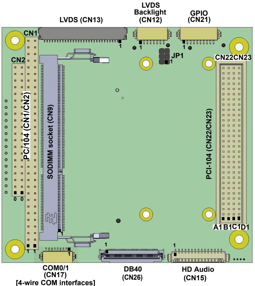
![LVDS (CN13)\nLVDS\nBacklight\n(CN12)\nGPIO\n(CN21)\nCN1\n1\n1\n1\nJP1\nCN22CN23\nCN2\nPC/104 (CN1/CN2)\nSODIMM socket (CN9)\nPCI-104 (CN22/CN23)\nA1B1C1D1\nCOM0/1\n(CN17)\n(4-wire COM interfaces)\nDB40\n(CN26)\nHD Audio\n(CN15)](.cmx-btx-50m-95186-5000-50/86e6522ac8c3f87548f5d08dced20e4c3421f549c17fac961f43e660a734394e.jpg)

Figure 2-2: Header and Connector Locations (bottom side)

Table 2-2: Header and Connector Definitions (bottom side)

<table><tr><td>Connector</td><td>Description</td><td>Mating Connector</td></tr><tr><td>CN1/CN2</td><td>Standard PC/104 connector, male</td><td>Standard PC/104 connector, female</td></tr><tr><td>CN9</td><td>Standard DDR3L SODIMM socket</td><td>DDR3L memory module, non-buffered, non-ECC</td></tr><tr><td>CN12</td><td>LVDS Backlight connector, Hirose DF13, 1*8 pins, 1.25mm pitch (Hirose, DF13A-8P-1.25H)</td><td>Hirose, DF13-8S-1.25C with crimp contact DF13-2630 SCF</td></tr><tr><td>CN13</td><td>LVDS connector, Hirose DF19, 1*30 pins, 1.0mm pitch (Hirose, DF19G-30P-1H)</td><td>Hirose, DF19-30S-1C with crimp contact DF19A-3032 SCF A</td></tr><tr><td>CN15</td><td>HD Audio connector, Molex PicoBlade Header, 1*15 pins, 1.25mm pitch (Molex 53261-1571)</td><td>Molex PicoBlade female connector, (Molex 51021-1500)</td></tr><tr><td>CN17</td><td>COM0/1 connector, Hirose DF13, 1*9 pins, 1.25mm pitch (Hirose, DF13A9P-1.25H)</td><td>Hirose, DF13-9S-1.25C with crimp contact DF13-2630 SCF</td></tr><tr><td>CN21</td><td>User GPIO connector, Hirose DF13, 1*10 pins, 1.25mm pitch (Hirose, DF13A-10P-1.25H)</td><td>Hirose, DF13-10S-1.25C with crimp contact DF13-2630 SCF</td></tr><tr><td>CN22/CN23</td><td>Standard PCI-104 connector, male</td><td>Standard PC/104 connector, female</td></tr><tr><td>CN26</td><td>DB40 debug connector, FFC, 1*40 pins, 0.5mm pitch (Molex, 502790-4091)</td><td>FPC/FFC, 0.3mm thick (+/- 0.05mm) with 0.5mm pitch</td></tr><tr><td>JP1</td><td>LCD and Backlight voltage selection jumper block, 2*3 pins, 2.0mm pitch</td><td>2.0mm mini jumper</td></tr></table>

# 2.2 Mechanical Dimensions

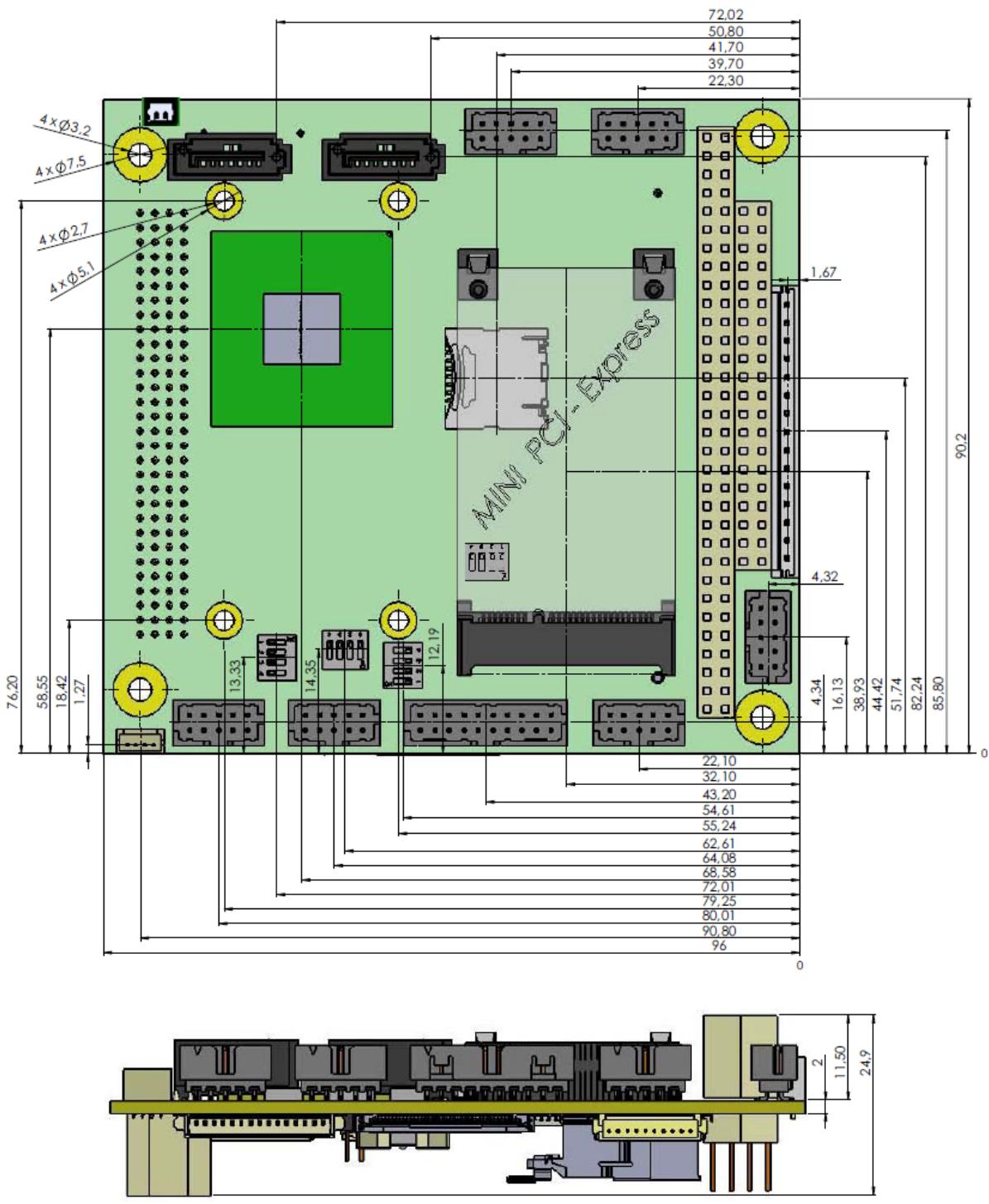
![72,02\n50,80\n41,70\n39,70\n22,30\n4xØ3.2\n4xØ7.5\n4xØ2.7\n4xØ5.1\n76,20\n58,55\n18,42\n1,27\n13,33\n14,35\n12,19\nMINI PCI-Express\n1,67\n90,2\n4,32\n4,34\n16,13\n38,93\n44,42\n51,74\n82,24\n85,80\n0\n22,10\n32,10\n43,20\n54,61\n55,24\n62,61\n64,08\n68,58\n72,01\n79,25\n80,01\n90,80\n96\n0\n2 11,50 24,9](.cmx-btx-50m-95186-5000-50/3fd6255920922a3bb9ce35eaec929ae2c89e6344da99d265ed702a3d96ebc1ba.jpg)

Figure 2-3: Mechanical Dimensions

![The image displays a graphic icon of a white document with a folded top-right corner and a large red checkmark. To the right of the icon is the text 'NOTE::' in black, capitalized serif letters.](.cmx-btx-50m-95186-5000-50/96c42c6df2a040f0a6cbf69e937e9892c4c93dc88a9cd2890afaf10e465ac724.jpg)

Mechanical dimensions in Figure 2-3 shown in millimeters.

# 2.3 LED Indicators

All LEDs are located on the top-side, board edge shown in Figure 2-1. See Figure 2-4 for LED locations and Table for LED function definitions.

![LED3\nLED4\nLED2\nLED1\nLED8\nLED10\nLED9\nLED13\nLED12\nLED11\nLED7\nLED6\nLED5](.cmx-btx-50m-95186-5000-50/d5425b6052a6d7c684c45571b4555de4f40407863f5bcf41d69a35c27ee31198.jpg)

Figure 2-4: LED Locations

Table 2-3: LED Definitions

<table><tr><td>LED#</td><td>Color</td><td>Function</td></tr><tr><td>LED10</td><td>red</td><td>Watchdog indicator LED</td></tr><tr><td>LED1</td><td>green</td><td>HDD Activity indicator LED</td></tr><tr><td>LED8</td><td>blue</td><td>BMC Status indicator LED</td></tr><tr><td>LED4</td><td>green</td><td>mini-PCIe WPAN Connection indicator LED</td></tr><tr><td>LED3</td><td>green</td><td>mini-PCIe WLAN Connection indicator LED</td></tr><tr><td>LED2</td><td>green</td><td>mini-PCIe WWAN Connection indicator LED</td></tr><tr><td>LED7</td><td>yellow</td><td>Gbit Ethernet Speed = 1000 Mbit/s indicator on ETH1</td></tr><tr><td>LED6</td><td>yellow</td><td>Gbit Ethernet Activity indicator on ETH1</td></tr><tr><td>LED5</td><td>green</td><td>Gbit Ethernet Speed = 100 Mbit/s indicator on ETH1</td></tr><tr><td>LED9</td><td>green</td><td>Power Good indicator LED</td></tr><tr><td>LED13</td><td>yellow</td><td>Gbit Ethernet Speed = 1000 Mbit/s indicator on ETH2</td></tr><tr><td>LED12</td><td>yellow</td><td>Gbit Ethernet Activity indicator on ETH2</td></tr><tr><td>LED11</td><td>green</td><td>Gbit Ethernet Speed = 100 Mbit/s indicator on ETH2</td></tr></table>

# 2.4 Hardware Setup

![The image shows a yellow triangular warning sign with a black border. Inside the triangle is a black exclamation mark.](.cmx-btx-50m-95186-5000-50/9c4549e0e514a46d477bf4f03ae07b36f6345b169a9ee36bc0f89196108f1126.jpg)
CAUTION:

MISE EN GARDE

Be sure to observe the EMC security measures. Make sure you are always at the same potential as the module.

Assurez-vous de respecter les mesures de sécurité CEM. Assurez-vous que vous êtes toujours au même potentiel que le module.

![A yellow triangular warning sign with a black border featuring a large black exclamation mark in the center.](.cmx-btx-50m-95186-5000-50/07acbeb7cc45f69f5dc547a19bc4104eb8a8638860e218cc8c2277c892e0f74a.jpg)
CAUTION:

MISE EN GARDE

Never connect or disconnect peripherals like HDDs, PCI, and ISA boards while the board’s power supply is connected and switched on.

Ne connectez ou ne déconnectez jamais des périphériques tels que des disques durs, des cartes PCI et ISA lorsque l’alimentation de la carte est connectée et sous tension.

![The image displays a white document icon with a folded top-right corner. Faint gray horizontal lines represent text on the page. A large, bold red checkmark is superimposed over the center of the document, indicating approval or completion.](.cmx-btx-50m-95186-5000-50/3e72ea86b5fa16a71367356c9987086a549e9e45e1b7dd36caa3c3630ceacfe3.jpg)
NOTE:

Refer to Table 1-2 on page 3 for a list of cables included in the optional cable set.

Use the following four steps to mount the heat spreader to the top side of the board, covering the CPU and voltage regulators with the thermal pads on the heat spreader. The heat spreader provides a neutral plane for mounting a custom heat sink.

![Two views of a transparent container with blue liquid, one highlighted in yellow (no text or symbols visible)](.cmx-btx-50m-95186-5000-50/7fa87c0932afb3aac53ad9f1e04d08d3c8b1bf20a7f7bcdad997e0e718ce61aa.jpg)

1. Remove the protective membranes from the thermal pads on the heat spreader.

![Two electronic circuit boards with integrated circuits and connectors, one showing a green highlighted component (no visible text or symbols)](.cmx-btx-50m-95186-5000-50/f6e0d99d4d9afc3f058ea55487ed45898fde1274f456278aa53fc36a99145d3a.jpg)

2. Align the thermal pad on the heat spreader, designated for the CPU, with the CPU on the board.

![Close-up of a printed circuit board with integrated circuits and connectors (no visible text or symbols)](.cmx-btx-50m-95186-5000-50/6c7e0d43b1cbbf1ab4d67efa550cbad0fe92ece8736c928a0e2f340e6f89a3e8.jpg)

3. Turn over the heat spreader and place it on top of the board so that the four mounting holes line up with the holes on the board and the thermal pads cover the CPU and voltage regulators on the board.

![Close-up of a printed circuit board with visible components and connectors (no readable text or symbols)](.cmx-btx-50m-95186-5000-50/395c79d0026fe908964371a10788e2269b6348e3f150f16c2382b86ca40427b5.jpg)

4. Turn over the board and install four M2.5, pan head, L8 mounting screws at 3kgf. cm torque in the four mounting holes on the board.

Install up to 4GB of DDR3L SODIMM memory in the CN9 SODIMM socket.

Connect a USB keyboard and optionally a USB mouse to the appropriate headers on the board. Use a USB hub to expand the device connections, if necessary. Use the SATA  cable to connect the hard disk. Make sure that the pins match their counterparts correctly and are not twisted. If you plan to use additional peripherals, connect them to the appropriate headers.

Connect a 5-volt, 3-amp power supply to the power connector and switch on the power.

![The image displays a graphic of a white document page with faint horizontal lines. A large red checkmark is stamped diagonally across the center of the page. Beneath the document graphic, the text 'NOTE:' appears in black capital letters.](.cmx-btx-50m-95186-5000-50/437625e5d3b59ad147412990172a46f265a317627e0a8d5dab87840b5aa716ef.jpg)

The system will function with only 5V power input. Additional 12V input is only necessary if using an external LVDS panel.

The display shows the BIOS messages. If you want to change the standard BIOS settings, press the &lt;DEL&gt; key to enter the BIOS menu. See Chapter 4 for setup details.

If you need to load the BIOS default values, they can be automatically loaded at boot time. The CMx-BTx boots from SATA hard disk drives, CD drives, USB floppies, USB sticks, hard disks, or from a Micro SD card inserted in the optional Micro SD slot, if installed.

Provided that any of these is connected and contains a valid operating system image, the display then shows the boot screen of your operating system.

The CMx-BTx needs adequate cooling measures depending on the desired operating temperature range. Using the board without cooling could damage the board permanently. See Table 1-9 on page 5.

# 2.5 Windows 10 Installation

To install Windows 10 on the system, change the following settings in the BIOS. Refer to “BIOS Setup” on page 47 for information on how to enter BIOS setup.

# "Advanced" >"BayTrail Features Configuration"

![Aptio Setup Utility - Copyright (C) 2018 American Megatrends, Inc.\nMain Advanced Security Boot Save & Exit\nCPU Configuration GrBaytrail Features\nGraphics Configuration rCoConfiguration - LPSS/SSC\nSATA Configuration r\nUSB Configuration r\nSDIO Configuration r\nNetwork Configuration r\nAudio Configuration r\nPCI/PCIe Configuration r\nBaytrail Features Configuration r\nACPI Settings r\nSerial Port Console Redirection r)(: Select Screen\nThermal Configuration r: Select Item\nSecurity Configuration rEnter: Select\nMiscellaneous r+/-: Change Opt.\nNCT5104D Super IO Configuration rF1: General Help\nEthernet Controls rF2: Previous Values\nMini-PCIe-slot function rF9: Optimized Defaults\nUSB Controls F10: Save & Exit\nESC: Exit\nVersion 2.17.1246. Copyright (C) 2018 American Megatrends, Inc. B4](.cmx-btx-50m-95186-5000-50/12944cbf39d3eca228a91e674018a9dc45e98bd5dda883207be8c34a2318d033.jpg)

# "LPSS & SCC Devices Mode"

![Aptio Setup Utility - Copyright (C) 2018 American Megatrends, Inc.\nAdvanced\nLPSS & SCC Devices Mo (PCI mode)\nSCC Configuration\nSCC SD Card Support (Enabled)\nSDR25 Support for SDC (Enabled)\nDDR50 Support for SDC (Disabled)\nMIPI HSI Support (Disabled)\nLPSS Configuration\nLPSS HSUART #1 Suppor (Disabled)\nLPSS & SCC Devices Mode\nSettings\n((: Select Screen\n: Select Item\nEnter: Select\n+/-: Change Opt.\nF1: General Help\nF2: Previous Values\nF9: Optimized Defaults\nF10: Save & Exit\nESC: Exit\nVersion 2.17.1246. Copyright (C) 2018 American Megatrends, Inc.](.cmx-btx-50m-95186-5000-50/863e68b7ab60ebdab403b1718d5a69c95557c4e69b93f0bb5139fb02a6abe0ab.jpg)

# Set to "ACPI mode"

![Aptio Setup Utility - Copyright (C) 2018 American Megatrends, Inc.\nAdvanced\nLPSS & SCC Devices Mo (ACPI mode)\nSCC Configuration\nSCC SD Card Support (Enabled)\nSDR25 Support for SDC (Enabled)\nDDR50 Support for SDC (Disabled)\nMIPI HSI Support (Disabled)\nLPSS & SCC Devices Mode\nLPSS Configuration\nLPSS HSUART #1 Suppo\nACPI mode\nPCI mode\nLPSS & SCC Devices Mode Settings\nSelect Screen\nElect Item\nEnter: Select\n+/-: Change Opt.\nF1: General Help\nF2: Previous Values\nF9: Optimized Defaults\nF10: Save & Exit\nESC: Exit\nVersion 2.17.1246. Copyright (C) 2018 American Megatrends, Inc.](.cmx-btx-50m-95186-5000-50/f9a75563ed796024f9f327456bc1830f376f9bd26bbf2f5d1905eb108c10c3e2.jpg)

You can now perform a fresh installation of Windows 10 64-bit.

# 3 Module Description

# 3.1 SoC (System on a Chip)

The Intel® Atom™ E3800 product series features an Intel® Architecture (IA) that integrates the next generation Intel processor core, graphics engine, memory controller, and I/O interfaces into a single SoC solution, which is based upon the Intel 22nm process technology.

# 3.1.1 Processor Core

 Up to four IA-compatible low power Intel® processor cores, one thread per core
 Two-wide instruction decode, out of order execution
 On-die, 32 KB 8-way L1 instruction cache and 24 KB 6-way L1 data cache per core
 On-die, 1 MB, 16-way L2 cache, shared per two cores
 36-bit physical address, 48-bit linear address size support
 Supported C-states: C0, C1, C1E, C6C, C6
 Supports Intel® Virtualization Technology (Intel® VT-X)

# 3.1.2 Memory Controller

 Supports up to two channels of 64-bit data bus DDR3L-RS SDRAM (only one is supported on the CMx-BTx family of modules)
 Supports x16 DDR3L-RS SDRAM devices
 Supports DDR3L-RS with 1066 or 1333 MT/s data rates (type is bound to the specific SoC)
 Total memory bandwidth supported is 8.5 GB/s for 1066 MT/s single channel up to 21.3 GB/s for 1333 MT/s dual channel (not supported on the CMx-BTx family of boards)
 Supports different physical mappings of bank addresses to optimize performance
 Out-of-order request processing to increase performance
 Aggressive power management to reduce power consumption
 Proactive page closing policies to close unused pages

# 3.1.3 Graphics Engine

 Intel’s 7th generation (Gen 7) graphics and media encode/decode engine
 VED video decoder in addition to Gen 7 Media decoder
 Supports DX 11, OpenGL 3.0 (OGL 3.0), OpenCL 1.2 (OCL 1.2), OpenGLES 2.0 (OGLES 2.0)
 GPU shader is capable of up to 8 gigaflops
 4x anti-aliasing
 Full HW acceleration for decode of H.264, MPEG2, MVC, VC-1, VP8, MJPEG
 Full HW acceleration for encode of H.264, MPEG2, MVC
 Supports 2.0 Stereoscopic 3D stretch
 Polyphase 8 tap scaling
 HD HQV
 Intel® Burst Technology
 Intel® Display Power Saving Technology (Intel® DPST) 6.0
 Intel® Display Refresh Rate Switching Technology (Intel® DRRS Technology)
 PSR (Panel self refresh)

# 3.1.4 Image Signal Processor

 Integrated MIPI-CSI 2.0 interface (not supported on the CMx-BTx modules)

# 3.1.5 Power Management

 ACPI 5.0 support
 Processor states: C0 – C6
 Display device states: D0, D3
 Graphics device states: D0, D3
 System sleep states: S0, S3, S4, S5 (S4 and S5 are the same for this SoC)
 Dynamic I/O power reductions (disabling sense amps on input buffers, tri-stating output buffers)
 Conditional memory self-refresh during C2
 Active power-down of display links
 Downloadable power management firmware

# 3.1.6 PCI Express

On the CMx-BTx, the PCI Express bus is configured as four root ports, where each is configured as a x1 port (2.5 GT/s). The function of each port is shown in the table below:

Table 3-1: PCIe Port Functions

<table><tr><td>Root port#</td><td>Function/Description</td></tr><tr><td>Port 0</td><td>Gigabit Ethernet Channel 0 (ETH1)</td></tr><tr><td>Port 1</td><td>Gigabit Ethernet Channel 1 (ETH2)</td></tr><tr><td>Port 2</td><td>PCI Express to PCI Bridge for the PCI-104 Interface (XIO2001)</td></tr><tr><td>Port 3</td><td>mini-PCIe socket for PCI Express extension cards</td></tr></table>

Each of the four ports supports the WAKE function.

# 3.1.7 SATA Controller

 Up to two SATA 3 Gb/s ports
 Legacy IDE (including IRQ)/Native IDE/AHCI appearance to OS
 Partial/Slumber power management modes with wake
 Supports RunTime D3

# 3.1.8 USB xHCI Controller

 Supports USB 2.0/1.1
 Implements xHCI software host controller interface
 Four ports multiplexed with EHCI controller that are High Speed/Full Speed (HS/FS)

# 3.1.9 USB 2.0 EHCI Controller

 Internal Rate Matching Hub to support USB 1.1 to 2.0 devices
 Four Ports multiplexed with xHCI controller
 Enhanced EHCI descriptor caching

# 3.1.10 HD-Audio Controller

 Four In and four Out streams, where only three are used
 No wake on audio (modem) support

# 3.1.11 Intel® Trusted Execution Engine (Intel® TXE)

Intel TXE system contains a security engine and additional hardware security features that enable a secure and robust platform. The security features include:

 Isolated execution environment for crypto operations (SKU-enabled)
 Supports secure boot – with customer programmable keys to secure code

![The image shows a white document icon with a folded top-right corner. Horizontal grey lines run across the page to simulate text, and a large, bold red checkmark is superimposed diagonally across the document.](.cmx-btx-50m-95186-5000-50/5563f99e8b3ad030f0c8974c32af64dbf4759e2f7ad7fcae24f0d8a38ca5bff0.jpg)
NOTE:

The SoC requires TXE firmware in the PCU SPI flash image to function.

# 3.1.12 Platform Control Unit (PCU)

The SoC provides the following PCU HW blocks:

 SMBus
 SPI interface for flash only (boot FW and system configuration data)
 RTC, Interrupts, Timers, GPIOs, and LPC interface

# 3.2 VGA Interface

The CMx-BTx supports a VGA interface originating from the SoC and provides the signals through the CN14, 10-pin, 2.0mm header.

Table 3-2: VGA Header Signals (CN14)

<table><tr><td>Pin</td><td>Signal</td><td>Pin</td><td>Signal</td><td rowspan="6">&lt;img src="images/cf801149257ecb0306d4a3c8d6e53c9112d24bb36498e439b8f43cb01f73869f.jpg"/&gt;</td></tr><tr><td>1</td><td>Red</td><td>2</td><td>GND</td></tr><tr><td>3</td><td>Green</td><td>4</td><td>GND</td></tr><tr><td>5</td><td>Blue</td><td>6</td><td>VGA_DDC_CLK</td></tr><tr><td>7</td><td>HSYNC</td><td>8</td><td>VGA_DDC_DATA</td></tr><tr><td>9</td><td>VSYNC</td><td>10</td><td>GND</td></tr></table>

# 3.3 LVDS Interface

The LVDS interface is connected to the DDI0 interface of the SoC, while the translation is made by a NXP PTN3460IBS (e)DisplayPort™ to LVDS converter.

The NXP PTN3460IBS supports the following features:

 2-Lane Display Port receiver
 2-Port LVDS output interface
 Max. Resolution up to 1920 x 1200 x 60 (RB), 18-bit color depth (24-bit color depth on smaller resolutions)
 Supports 2-lane digital input, with speeds up to 1.62/2.7Gbps
 Supports dual port, 6/8-bits LVDS output
 QFN-48 Pin package

The LVDS interface is accessible at connector CN13 (Bottom Side), which is a Hirose DF19-30 (1.0 mm pitch) with the following pin definitions:

Table 3-3: LVDS Signal Definitions (CN13)

<table><tr><td>Pin#</td><td>Interface</td><td>Signals</td><td>Comment</td></tr><tr><td>1</td><td rowspan="3">Panel Power Supply</td><td>+VCC_LCD_L_CN</td><td rowspan="2">Can be configured at the “CN_PANEL_VCC_SEL1” jumper block (JP1)</td></tr><tr><td>2</td><td>+VCC_LCD_L_CN</td></tr><tr><td>3</td><td>GND</td><td></td></tr><tr><td>4</td><td>Power Supply/Shield</td><td>GND</td><td></td></tr><tr><td>5</td><td rowspan="11">Data Channel A</td><td>LA_DATA3_N_L</td><td></td></tr><tr><td>6</td><td>LA_DATA3_P_L</td><td></td></tr><tr><td>7</td><td>LA_CLK_N_L</td><td></td></tr><tr><td>8</td><td>LA_CLK_P_L</td><td></td></tr><tr><td>9</td><td>GND</td><td></td></tr><tr><td>10</td><td>LA_DATA2_N_L</td><td></td></tr><tr><td>11</td><td>LA_DATA2_P_L</td><td></td></tr><tr><td>12</td><td>LA_DATA1_N_L</td><td></td></tr><tr><td>13</td><td>LA_DATA1_P_L</td><td></td></tr><tr><td>14</td><td>LA_DATA0_N_L</td><td></td></tr><tr><td>15</td><td>LA_DATA0_P_L</td><td></td></tr><tr><td>16</td><td>Shield</td><td>GND</td><td></td></tr><tr><td>17</td><td rowspan="11">Data Channel B</td><td>LB_DATA3_N_L</td><td></td></tr><tr><td>18</td><td>LB_DATA3_P_L</td><td></td></tr><tr><td>19</td><td>LB_CLK_N_L</td><td></td></tr><tr><td>20</td><td>LB_CLK_P_L</td><td></td></tr><tr><td>21</td><td>GND</td><td></td></tr><tr><td>22</td><td>LB_DATA2_N_L</td><td></td></tr><tr><td>23</td><td>LB_DATA2_P_L</td><td></td></tr><tr><td>24</td><td>LB_DATA1_N_L</td><td></td></tr><tr><td>25</td><td>LB_DATA1_P_L</td><td></td></tr><tr><td>26</td><td>LB_DATA0_N_L</td><td></td></tr><tr><td>27</td><td>LB_DATA0_P_L</td><td></td></tr><tr><td>28</td><td>Shield</td><td>GND</td><td></td></tr><tr><td>29</td><td rowspan="2">DDC Channel</td><td>LVDS_DDC_L_CLK</td><td></td></tr><tr><td>30</td><td>LVDS_DDC_L_DATA</td><td></td></tr><tr><td>31</td><td rowspan="2">Case/Shield</td><td>GND</td><td rowspan="2"></td></tr><tr><td>32</td><td>GND</td></tr><tr><td colspan="4">Connector</td></tr><tr><td colspan="4">&lt;img src="images/da1dbaac04c93b550945e0ce0b78489752f6239a255527b274835a1cf8c4b80b.jpg"/&gt;</td></tr></table>

# 3.4 LVDS Backlight

The backlight can be enabled/disabled from the BIOS setup. The backlight dimming source can be configured from the BIOS setup. These options originate from the SoC or from the BMC.

The connector (CN12) to which the backlight can be attached, is a Hirose DF13-8 with the following pin out:

Table 3-4: LVDS Backlight Signal Definitions (CN12)

<table><tr><td>Pin#</td><td>Signal</td><td>Comment</td></tr><tr><td>1</td><td rowspan="4">+VCC_BLK</td><td rowspan="4">Routed from JP1 as configured through the jumper setting on JP1 (5V or 12V, 12V = default)</td></tr><tr><td>2</td></tr><tr><td>3</td></tr><tr><td>4</td></tr><tr><td>5</td><td>LVDS_BKLT_CTRL</td><td>PWM output for Backlight dimming (SoC | BMC)</td></tr><tr><td>6</td><td>BKL_EN_OUT</td><td>Backlight enable signal; turns on simultaneously with the +VCC_LCD voltage</td></tr><tr><td>7</td><td>GND</td><td rowspan="2"></td></tr><tr><td>8</td><td>GND</td></tr><tr><td colspan="3">Connector</td></tr><tr><td colspan="3">&lt;img src="images/b911c82529aebe5beda72f55879a4234d163b8176949ec64556d73878eb8c137.jpg"/&gt;</td></tr></table>

# 3.4.1 Selecting Panel and Backlight voltage

At the jumper block “CN\_PANEL\_VCC\_SEL1” (JP1), both voltages can be configured using a 2mm jumpers.

Table 3-5: LVDS Backlight Voltage Select Signals (JP1)

<table><tr><td>Pin#</td><td>Signal</td><td>Pin#</td><td>Signal</td></tr><tr><td>1</td><td>+V3P3S (default)</td><td>2</td><td>+V12P0_ATX (default)</td></tr><tr><td>3</td><td>+VCC_LCD</td><td>4</td><td>+VCC_BKL</td></tr><tr><td>5</td><td>+V5P0_ATX</td><td>6</td><td>+V5P0_ATX</td></tr></table>

![Backlight\nJP1\n6 5\n4 3\n2 1](.cmx-btx-50m-95186-5000-50/fd123917fd1e6788abaae6643f1882e8c10b54da0fe03fa4fff9ce895a01fcfc.jpg)

# 3.5 Ethernet Controllers

Up to two Intel® I210IT Gigabit Ethernet controllers are supported with the following capabilities:

 PCIe v2.1 (2.5 GT/s) x1, with switching Voltage Regulator (iSVR)
 Integrated Non-Volatile Memory (iNVM)
 Platform Power Efficiency

 IEEE 802.3az Energy Efficient Ethernet (EEE)
 Proxy: ECMA-393 and Windows logo for proxy offload
 Converged Platform Power Management (CPPM)/(DMAC, LTR, OBFF)

 Advanced Features:

 $\angle 4 0 ^ { \circ } \mathsf { C }$ to $8 5 ^ { \circ } \mathsf { C }$ Industrial temperature
 Audio-video bridging

\- IEEE 1588/802.1AS precision time synchronization

\- IEEE 802.1Qav traffic shaper (with software extensions)

 Jumbo frames
 Interrupt moderation, VLAN support, IP checksum offload
 PCIe OBFF (Optimized Buffer Flush/Fill) for improved system power management
 Four transmit and four receive queues
 RSS and MSI-X to lower CPU utilization in multi-core systems
 Advanced cable diagnostics, auto MDI-X
 ECC – error correcting memory in packet buffers
 Four Software Definable Pins (SDPs)

 Manageability:

 NC-SI for greater bandwidth pass through
 SMBus low-speed serial bus to pass network traffic
 Flexible firmware architecture with secure Flash update
 MCTP over SMBus/PCIe
 OS2BMC/CEM (optionally enabled via external Flash)
 PXE and iSCSI boot

Each Ethernet interface is accessible through a 2\*5, 2.0 mm pin header from Molex.

Table 3-6: Ethernet Signal Definitions (CN10/CN11)

<table><tr><td>Pin#</td><td>Signal</td><td>Pin#</td><td>Signal</td></tr><tr><td>1</td><td>MX1-</td><td>2</td><td>MX1+</td></tr><tr><td>3</td><td>MX2-</td><td>4</td><td>MX2+</td></tr><tr><td>5</td><td>n.c. (optional PE)</td><td>6</td><td>n.c.</td></tr><tr><td>7</td><td>MX3-</td><td>8</td><td>MX3+</td></tr><tr><td>9</td><td>MX4-</td><td>10</td><td>MX4+</td></tr><tr><td colspan="4">Connector</td></tr></table>

![GbE1 CN10\nGbE2 CN11\n2\n1\n2\n1](.cmx-btx-50m-95186-5000-50/1014e1880ae0f5e3dbba80968b3a84087134f23f754dc6b1fa360f4f3ae56e8d.jpg)

# 3.6 USB Ports

The module supports up to four USB connections: three USB 2.0 High Speed ports, and one USB 2.0 High Speed port routed to the mini-PCIe socket.

The three USB 2.0 ports are combined on a $2 ^ { \star } 1 0$ pin, 2.0 mm pitch header from Molex.

![The image displays a standard yellow triangular warning sign with a black border. Inside the triangle is a large black exclamation point. Directly below the triangle, the text 'CAUTION:' is printed in bold black capital letters.](.cmx-btx-50m-95186-5000-50/c8923a0e9a6bb2538db8371febd1db2eedd4f964df207f86754cee3b4186bab3.jpg)
MISE EN GARDE

It is not recommended to draw more than 2.0 A in total over all three USB ports, where each port is limited to approximately 680 mA. (Exception: On USB#0, 1000 mA is allowed.)

Il n'est pas recommandé de tirer plus de 2,0 A au total sur les trois ports USB, où chaque port est limité à environ 680 mA. (Exception: sur USB # 0, 1000 mA est autorisé.)

The signals of this header are defined in the following table.

Table 3-7: USB Signal Definitions (CN16)

<table><tr><td>Pin</td><td>Interface</td><td>Signals</td><td>Connector120</td><td>Pin</td><td>Interface</td><td>Signals</td></tr><tr><td>1</td><td rowspan="10">USB #0</td><td>+VCC_USB0</td><td rowspan="11">&lt;img src="images/8d09ae32d61991a9cbfb46b8de8ae90256f3ad080d942ad4295f25637f8d0e7c.jpg"/&gt;</td><td>20</td><td rowspan="10">USB #1 &amp; #2</td><td>N.C.</td></tr><tr><td>2</td><td>USB3_P0_L_RXN</td><td>19</td><td>+VCC_USB1</td></tr><tr><td>3</td><td>USB3_P0_L_RXP</td><td>18</td><td>N.C.</td></tr><tr><td>4</td><td>GND</td><td>17</td><td>+VCC_USB2</td></tr><tr><td>5</td><td>USB3_P0_L_TXN</td><td>16</td><td>GND</td></tr><tr><td>6</td><td>USB3_P0_L_TXP</td><td>15</td><td>USB2_P2_L_DN</td></tr><tr><td>7</td><td>GND</td><td>14</td><td>USB2_P2_L_DP</td></tr><tr><td>8</td><td>USB2_P0_L_DN</td><td>13</td><td>GND</td></tr><tr><td>9</td><td>USB2_P0_L_DP</td><td>12</td><td>USB2_P1_L_DN</td></tr><tr><td>10</td><td>N.C.</td><td>11</td><td>USB2_P1_L_DP</td></tr><tr><td colspan="3"></td><td colspan="3"></td></tr></table>

# 3.7 On-Board Power Supply

There are two resistor configuration options available for the CMx-BTx that can be selected at the time of build (available on A5 version only).

In the default configuration, the CMx-BTx devices can be run with only 5 volts. If a Standby mode is needed, the 5V Standby voltage has to be connected in addition to the 5V supply. In this configuration, externally generated PCI\_3V3 should not be applied to the CMx-BTx.

The +12V supply is only needed for driving an LCD backlight.

All other voltages needed to run the module are generated on the module itself.

In an alternate configuration (contact ADLINK for further information), PCI\_3V3 power is not generated on the module and instead can and should be powered externally by the stackable PCI-104 connector (available on A5 version only).

In both configurations, main +5V and LCD backlight +12V power can be supplied over the power connector, PCI-104 connector, or the PC/104 connector. 5V Standby power can be supplied over the power connector or the PCI-104 connector, but not the PC/104 connector.

The power connector is a JST-B15B-EH, 1.5 mm pitch single row connector. The cable kit provides an adapter cable to convert from this to a standard 20-pin ATX connector.

Table 3-8: Power Signal Definitions (CN24)

<table><tr><td>Pin#</td><td>Signal</td><td>Pin#</td><td>Signal</td></tr><tr><td>1</td><td>+V5P0_ATX</td><td>2</td><td>GND</td></tr><tr><td>3</td><td>+V5P0_ATX</td><td>4</td><td>GND</td></tr><tr><td>5</td><td>+V5P0_ATX</td><td>6</td><td>+V5P0ATX_SBY</td></tr><tr><td>7</td><td>GND</td><td>8</td><td>ATX_PSON#</td></tr><tr><td>9</td><td>ATX_PWRGD</td><td>10</td><td>+V3P3_ATX</td></tr><tr><td>11</td><td>GND</td><td>12</td><td>+V12P0_ATX</td></tr><tr><td>13</td><td>+V12P0_ATX</td><td>14</td><td>GND</td></tr><tr><td>15</td><td>-V12P0_ATX</td><td></td><td></td></tr><tr><td colspan="4">Connector</td></tr><tr><td colspan="4">&lt;img src="images/5852811cbacf6d45f8b4cd3e607f86da22ce94be07d1434830fe4d3e6732756a.jpg"/&gt;</td></tr></table>

# 3.8 System Panel

The System Panel interface provides signals for external speakers, HDD LEDs, and power and reset buttons. The HDD-LED (K) on pin 7 includes a 680 Ohm series resistor for current limiting. The Anode of the LED should be connected to pin 2 (+V3P3S.)

For the speaker, ADLINK recommends speaker impedance at 8Ohm to 50Ohm and speaker power rating up to 1.0W.

The +V3P3S signal on pin 2 is fused with a slow-acting PTC-like, 750mA fuse. The same is true for the SPKR-OUT (+) signal on pin 3, but it is not recommended to draw more than 200mA from pin 3.

The cable set provided includes a cable for the system panel, which includes a power and reset button, while the other wires are open-end. The PMC\_RSTBTN\_IN# (reset) includes a 1k pullup resistor to a switched 3.3V, while the PS\_PWRBTN\_IN# includes a 3k3 pull up to an always on 3.3V.

![The image features a white document icon with a folded top-right corner. A large red checkmark is placed over the document, and faint horizontal lines are visible at the bottom. Below the icon, the text 'NOTE:' appears in black capital letters.](.cmx-btx-50m-95186-5000-50/1c11c9bead90230921d8d4ed9aae7d3407d4c786011b3d5f8b4a9df85e646e9c.jpg)

To connect an external RTC battery, use the system panel, open-end cable wires connected to pin 5 and pin 8 on CN20.

Table 3-9: System Panel Interface (CN20)

<table><tr><td>Pin</td><td>Signal</td><td>Pin</td><td>Signal</td></tr><tr><td>1</td><td>SPKR-IN (-)</td><td>2</td><td>+V3P3S</td></tr><tr><td>3</td><td>SPKR-OUT (+)</td><td>4</td><td>GND</td></tr><tr><td>5</td><td>+VCC_RTC_EXT</td><td>6</td><td>PS_PWRBTN_IN#</td></tr><tr><td>7</td><td>HDD-LED (K)</td><td>8</td><td>GND</td></tr><tr><td>9</td><td>WDTOUT</td><td>10</td><td>PMC_RSTBTN_IN#</td></tr></table>

![CN20\n1](.cmx-btx-50m-95186-5000-50/fcb3a50b6056d8a14da6c5fd18410d1d399aa27b88dce5404d32ddaed213d114.jpg)

The following table defines the pin assignments of the System Panel functions.

Table 3-10: System Panel Pin Assignments

<table><tr><td>Function</td><td>Related Pins</td></tr><tr><td>Power Button</td><td>4 and 6</td></tr><tr><td>Speaker</td><td>1 and 3</td></tr><tr><td>Reset</td><td>4 and 10</td></tr><tr><td>RTC-Battery</td><td>5 and 8</td></tr><tr><td>Watchdog-Out</td><td>8 and 9</td></tr><tr><td>HDD-LED</td><td>2 and 7</td></tr></table>

# 3.9 Serial Ports

The CMx-BTx module provides up to four serial ports through an LPC-to-UART Bridge (NCT5104D from Nuvoton.) All four serial ports are capable of running as RS232 or RS422, and each supports the following features:

 16650-compatible UART with 128-byte send/receive FIFO
 Programmable baud rate generator
 5, 6, 7 or 8-bit characters
 Even, odd or no parity bit generation / detection
 1, 1.5 or 2 stop-bit generation
 Loop-back controls for communications link fault isolation
 Break, parity, overrun, framing error simulation
 Speeds up to 115.2 kbaud in normal mode

 Up to 1.5 Mbaud in high speed mode (requires a custom BIOS, available on request)

The two COM ports COM2 and COM3 are fully implemented COM ports, supporting all nine defined signals, while the two COM ports COM0 and COM1 support only RXD, TXD and their corresponding handshake signals RTS# and CTS#.

The COM0 and COM1 are bundled on a Hirose DF13-9 connector (V) with the following pin out:

Table 3-11: COM0 and COM1 Serial Port Signal Definitions (CN17)

<table><tr><td>Pin#</td><td>RS232</td><td>RS422</td><td></td><td>DB9 - COM0</td><td>DB9 - COM1</td></tr><tr><td>1</td><td>COM0_RX</td><td>COM0_RX-</td><td></td><td>Pin 2</td><td>N/A</td></tr><tr><td>2</td><td>COM0_RTS#</td><td>COM0_TX+</td><td></td><td>Pin 7</td><td>N/A</td></tr><tr><td>3</td><td>COM0_TX</td><td>COM0_TX-</td><td></td><td>Pin 3</td><td>N/A</td></tr><tr><td>4</td><td>COM0_CTS#</td><td>COM0_RX+</td><td></td><td>Pin 8</td><td>N/A</td></tr><tr><td>5</td><td>GND</td><td>Not Used</td><td></td><td>Pin 5</td><td>Pin 5</td></tr><tr><td>6</td><td>COM1_RX</td><td>COM1_RX-</td><td></td><td>N/A</td><td>Pin 2</td></tr><tr><td>7</td><td>COM1_RTS#</td><td>COM1_TX+</td><td></td><td>N/A</td><td>Pin 7</td></tr><tr><td>8</td><td>COM1_TX</td><td>COM1_TX-</td><td></td><td>N/A</td><td>Pin 3</td></tr><tr><td>9</td><td>COM1_CTS#</td><td>COM1_RX+</td><td></td><td>N/A</td><td>Pin 8</td></tr><tr><td colspan="3"></td><td></td><td colspan="2">&lt;img src="images/e14a183d05476bdd0f0f5e1e9f0489186b94ddc62105ca6ccbe56dee2a0c4df5.jpg"/&gt;</td></tr><tr><td colspan="3">Connector</td><td></td><td colspan="2"></td></tr><tr><td colspan="6">&lt;img src="images/67177d12762d4eac277535bdb0576a49598941f23334b2f45eeff01d97f1cdea.jpg"/&gt;</td></tr></table>

Each of the COM2 and COM3 ports provides a Molex MilliGrid header with shroud and lock. The header pin signals are defined in the following table.

Table 3-12: COM2 and COM3 Serial Port Signal Definitions (CN18/CN19)

<table><tr><td>Pin#</td><td>RS232</td><td>DB9 Pin</td><td>Pin#</td><td>RS232</td><td>DB9 Pin</td></tr><tr><td>1</td><td>DCD#</td><td>1</td><td>2</td><td>DSR#</td><td>6</td></tr><tr><td>3</td><td>RXD</td><td>2</td><td>4</td><td>RTS#</td><td>7</td></tr><tr><td>5</td><td>TXD</td><td>3</td><td>6</td><td>CTS#</td><td>8</td></tr><tr><td>7</td><td>DTR#</td><td>4</td><td>8</td><td>RI#</td><td>9</td></tr><tr><td>9</td><td>GND</td><td>5</td><td>10</td><td>+V5P0S</td><td>Not connected</td></tr><tr><td colspan="6">Connector</td></tr><tr><td colspan="6">&lt;img src="images/fffa16c9b39973e89e7af82427c284a15df1478c86e2bd7e8edd636fd98983d5.jpg"/&gt;</td></tr></table>

# 3.10 Setting RS422 Termination

If the COM ports are used in RS422 modes, the termination resistors must be switched on. These are located at DIP-Switches SW2 and SW3 (SW4 is for BIOS configuration. See note.) The default setting is ${ } ^ { \mathfrak { w } } \mathsf { O F F } ^ { \mathfrak { w } }$ (RS232-Mode) as illustrated in the following table.

Table 3-13: SW2 and SW3 RS422 Signal Definitions

<table><tr><td>Position</td><td>Position</td><td>Signal(s)</td><td>Function</td></tr><tr><td>1</td><td>8</td><td>SW2: COM0-TXSW3: COM2-TX</td><td>Pos. 1: TX-termination offPos. 8: TX-termination on</td></tr><tr><td>2</td><td>7</td><td>SW2: COM0-RXSW3: COM2-RX</td><td>Pos. 2: RX-termination offPos. 7: RX-termination on</td></tr><tr><td>3</td><td>6</td><td>SW2: COM1-TXSW3: COM3-TX</td><td>Pos. 3: TX-termination offPos. 6: TX-termination on</td></tr><tr><td>4</td><td>5</td><td>SW2: COM1-RXSW3: COM3-RX</td><td>Pos. 4: RX-termination offPos. 5: RX-termination on</td></tr><tr><td colspan="4">DIP-Switches</td></tr><tr><td colspan="4">&lt;img src="images/d4c5195d96e265b593977522793d3d5446a65cc564f669a453aeccfeb75e5a4b.jpg"/&gt;</td></tr></table>

![The image shows a white document icon with a folded top-right corner and faint horizontal lines suggesting text. A large, bold red checkmark is superimposed over the center of the document.](.cmx-btx-50m-95186-5000-50/e169c6d32856b2b49dc5dc432533711955235e0e12430cbe686247da7083bba5.jpg)
NOTE:

The shaded table cells signify the default positions. Refer to Chapter 4 for the definition of the SW4 switch.

# 3.11 Mini-PCIe Interface

The Mini-PCIe interface, located on the top side of the module, provides expansion for PCIe, USB 2.0, and SSD devices as well as wireless applications. LEDs for WWAN, WLAN, and WPAN are implemented on the module, and the two disable lines for wireless expansion can be configured from the BIOS setup. Two modes can be configured from the BIOS setup for this socket:

 PCIe x1 mode
 mSATA mode, which shares the SATA interface with the SATA2 connector. When the socket is in mSATA mode, the SATA2 connector is disconnected from the SATA interface.

NOTE: Refer to Table 4-37 for Mini PCIe slot configuration settings.

The following table defines the Mini PCIe interface signals.

Table 3-14: Mini PCIe Signal Definitions (CN4)

<table><tr><td>Pin</td><td>Signal</td><td>Pin</td><td>Signal</td><td>Connector</td></tr><tr><td>1</td><td>MPCIE_WAKE# (3)</td><td>2</td><td>+V3P3S</td><td rowspan="27">&lt;img src="images/2dc6c5ac358c76ca15d3221584e44aac8c152e7717b41095ecfbd10b4d129912.jpg"/&gt;</td></tr><tr><td>3</td><td>N. C.</td><td>4</td><td>GND</td></tr><tr><td>5</td><td>N. C.</td><td>6</td><td>+V1P5S</td></tr><tr><td>7</td><td>MPCIE_CLKREQ# (3)</td><td>8</td><td>N. C.</td></tr><tr><td>9</td><td>GND</td><td>10</td><td>N. C.</td></tr><tr><td>11</td><td>PCIE_CLK3_N-</td><td>12</td><td>N. C.</td></tr><tr><td>13</td><td>PCIE_CLK3_P</td><td>14</td><td>N. C.</td></tr><tr><td>15</td><td>GND</td><td>16</td><td>N. C.</td></tr><tr><td colspan="4">Mechanical Key</td></tr><tr><td>17</td><td>N. C.</td><td>18</td><td>GND</td></tr><tr><td>19</td><td>N. C.</td><td>20</td><td>DISABLE_RADIO1#</td></tr><tr><td>21</td><td>GND</td><td>22</td><td>BUF_PLTRST#</td></tr><tr><td>23</td><td>MINICARD_RX_N</td><td>24</td><td>+V3P3S</td></tr><tr><td>25</td><td>MINICARD_RX_P</td><td>26</td><td>GND</td></tr><tr><td>27</td><td>GND</td><td>28</td><td>+V1P5S</td></tr><tr><td>29</td><td>GND</td><td>30</td><td>SMB_CLK</td></tr><tr><td>31</td><td>MINICARD_TX_N</td><td>32</td><td>SMB_DATA</td></tr><tr><td>33</td><td>MINICARD_TX_P</td><td>34</td><td>GND</td></tr><tr><td>35</td><td>GND</td><td>36</td><td>USB2_P3_DN</td></tr><tr><td>37</td><td>GND</td><td>38</td><td>USB2_P3_DP</td></tr><tr><td>39</td><td>+V3P3S</td><td>40</td><td>GND</td></tr><tr><td>41</td><td>+V3P3S</td><td>42</td><td>LED-W-WAN</td></tr><tr><td>43</td><td>GND</td><td>44</td><td>LED-W-LAN</td></tr><tr><td>45</td><td>N. C.</td><td>46</td><td>LED-W-PAN</td></tr><tr><td>47</td><td>N. C.</td><td>48</td><td>+V1P5S</td></tr><tr><td>49</td><td>N. C.</td><td>50</td><td>GND</td></tr><tr><td>51</td><td>DISABLE_RADIO2#</td><td>52</td><td>+V3P3S</td></tr></table>

# 3.12 PCI-104 Bus Interface

The CMx-BTx modules use a PCIe-to-PCI Bridge from Texas Instruments -- XIO2001 -- to achieve PCI bus compatibility, providing full PCI Express and PCI local bus functionality and performance.

The following list presents the key features of the PCI-104 bus interface.

 Fully compliant with the PCI Express to PCI/PCI-X Bridge Specification, Revision 1.0
 Fully compliant with the PCI Express Base Specification, Revision 2.0
 Fully compliant with the PCI Local Bus Specification, Revision 2.3
 Full x1 PCI Express throughput
 Capable of advanced error reporting
 Supports WAKE event and Beacon support
 Supports D1, D2, D3hot and D3cold
 Supports up to six external PCI Masters
 Advanced PCI Express Message Signaled Interrupt Generation for Serial IRQ Interrupts
 PCI Bus Interface 3.3V and 5.0V (25MHz or 33MHz only at 5.0V [solder jumper option]) Tolerance Options
 Active-State Link Power Management Saves Power When Packet Activity on the PCI Express Link is Idle, Using Both L0s and L1 States
 PCI-Express CLKREQ Support

The PCI-104 connector is located on the bottom side of the module, as shown in the drawing in the following table.

The following table defines the signals of the PCI-104 interface.

Table 3-15: PCI-104 Signal Definitions (CN22 / CN23)

<table><tr><td>Pin</td><td>Row A</td><td>Row B</td><td>Row C</td><td>Row D</td><td colspan="2">Connector</td></tr><tr><td>1</td><td>GND</td><td>+V5P0_SBY_</td><td>+V5P0_ATX</td><td>AD00</td><td rowspan="30">&lt;img src="images/a6c72a8318972c8fa8c96c9aa9d546f155289957b70ad8025a625aee34741b49.jpg"/&gt;</td><td rowspan="30"></td></tr><tr><td>2</td><td>+XPCI_VIO</td><td>AD02</td><td>AD01</td><td>+V5P0_ATX</td></tr><tr><td>3</td><td>AD05</td><td>GND</td><td>AD04</td><td>AD03</td></tr><tr><td>4</td><td>C/BE0#</td><td>AD07</td><td>GND</td><td>AD06</td></tr><tr><td>5</td><td>GND</td><td>AD09</td><td>AD08</td><td>GND</td></tr><tr><td>6</td><td>AD11</td><td>+XPCI_VIO</td><td>AD10</td><td>M66EN</td></tr><tr><td>7</td><td>AD14</td><td>AD13</td><td>GND</td><td>AD12</td></tr><tr><td>8</td><td>+V3P3_PCI</td><td>C/BE1#</td><td>AD15</td><td>+V3P3_PCI</td></tr><tr><td>9</td><td>SERR#</td><td>GND</td><td>ATX_PSON#</td><td>PAR</td></tr><tr><td>10</td><td>GND</td><td>PERR#</td><td>+V3P3_PCI</td><td>PME#</td></tr><tr><td>11</td><td>STOP#</td><td>+V3P3_PCI</td><td>LOCK#</td><td>GND</td></tr><tr><td>12</td><td>+V3P3_PCI</td><td>TRDY#</td><td>GND</td><td>DEVSEL#</td></tr><tr><td>13</td><td>FRAME#</td><td>GND</td><td>IRDY#</td><td>+V3P3_PCI</td></tr><tr><td>14</td><td>GND</td><td>AD16</td><td>+V3P3_PCI</td><td>C/BE2#</td></tr><tr><td>15</td><td>AD18</td><td>+V3P3_PCI</td><td>AD17</td><td>GND</td></tr><tr><td>16</td><td>AD21</td><td>AD20</td><td>GND</td><td>AD19</td></tr><tr><td>17</td><td>+V3P3_PCI</td><td>AD23</td><td>AD22</td><td>+V3P3_PCI</td></tr><tr><td>18</td><td>IDSEL0</td><td>GND</td><td>IDSEL1</td><td>IDSEL2</td></tr><tr><td>19</td><td>AD24</td><td>C/BE3#</td><td>+XPCI_VIO</td><td>IDSEL3</td></tr><tr><td>20</td><td>GND</td><td>AD26</td><td>AD25</td><td>GND</td></tr><tr><td>21</td><td>AD29</td><td>+V5P0_ATX</td><td>AD28</td><td>AD27</td></tr><tr><td>22</td><td>+V5P0_ATX</td><td>AD30</td><td>GND</td><td>AD31</td></tr><tr><td>23</td><td>REQ0#</td><td>GND</td><td>REQ1#</td><td>+XPCI_VIO</td></tr><tr><td>24</td><td>GND</td><td>REQ2#</td><td>+V5P0_ATX</td><td>GNT0#</td></tr><tr><td>25</td><td>GNT1#</td><td>+XPCI_VIO</td><td>GNT2#</td><td>GND</td></tr><tr><td>26</td><td>+V5P0_ATX</td><td>CLK0</td><td>GND</td><td>CLK1</td></tr><tr><td>27</td><td>CLK2</td><td>+V5P0_ATX</td><td>CLK3</td><td>GND</td></tr><tr><td>28</td><td>GND</td><td>INTD#</td><td>+V5P0_ATX</td><td>RST#</td></tr><tr><td>29</td><td>+V12P0_ATX</td><td>INTA#</td><td>INTB#</td><td>INTC#</td></tr><tr><td>30</td><td>-V12P0_ATX</td><td>REQ3#</td><td>GNT3#</td><td>GND</td></tr></table>

# 3.13 PC/104 Bus Interface

The PC/104 Bus Interface is implemented using a Fintek F85226FG LPC-to-ISA Bridge, capable of delivering a fully ISA, 16-bit compatible interface.

The Intel E3800 family of SoCs does not support the following features of the PC/104 interface:

 Bus Master Cycles
 DMA
 Memory Mapped transactions on the LPC bus
 IRQ0, Heartbeat Interrupt, which is generated off of the internal 8254 counter 0
 IRQ8, RTC interrupt can only be generated internally
 IRQ13, this Interrupt (floating point error) is not supported
 IRQ14, this Interrupt can only be generated by the SATA controller in Legacy mode
 ISA Enable (IE) bit is missing and therefore no automatic compensation for I/O address aliasing is available
 PnP

Table 3-16 defines the signals of the PC/104 connector.
Table 3-16: PC/104 Signal Definitions (CN1 / CN2)

<table><tr><td>Pin</td><td>Row D</td><td>Row C</td><td>Pin</td><td>Row A</td><td>Row B</td></tr><tr><td rowspan="8"></td><td rowspan="8"></td><td rowspan="8"></td><td>1</td><td>IOCHK#</td><td>GND</td></tr><tr><td>2</td><td>D7</td><td>RSTDRV</td></tr><tr><td>3</td><td>D6</td><td>+V5P0_ATX</td></tr><tr><td>4</td><td>D5</td><td>IRQ9</td></tr><tr><td>5</td><td>D4</td><td>N. C. (-5V)</td></tr><tr><td>6</td><td>D3</td><td>DRQ2</td></tr><tr><td>7</td><td>D2</td><td>-V12P0_ATX</td></tr><tr><td>8</td><td>D1</td><td>0WS#</td></tr><tr><td>0</td><td>GND</td><td>GND</td><td>9</td><td>D0</td><td>+V12P0_ATX</td></tr><tr><td>1</td><td>MEMCS16#</td><td>SBHE#</td><td>10</td><td>IOCHRDY</td><td>KEY</td></tr><tr><td>2</td><td>IOCS16#</td><td>LA23</td><td>11</td><td>AEN</td><td>SMEMW#</td></tr><tr><td>3</td><td>IRQ10</td><td>LA22</td><td>12</td><td>A19</td><td>SMEMR#</td></tr><tr><td>4</td><td>IRQ11</td><td>LA21</td><td>13</td><td>A18</td><td>IOW#</td></tr><tr><td>5</td><td>IRQ12</td><td>LA20</td><td>14</td><td>A17</td><td>IOR#</td></tr><tr><td>6</td><td>IRQ15</td><td>LA19</td><td>15</td><td>A16</td><td>DACK3#</td></tr><tr><td>7</td><td>IRQ14</td><td>LA18</td><td>16</td><td>A15</td><td>DRQ3</td></tr><tr><td>8</td><td>DACK0#</td><td>LA17</td><td>17</td><td>A14</td><td>DACK1#</td></tr><tr><td>9</td><td>DRQ0</td><td>MEMR#</td><td>18</td><td>A13</td><td>DRQ1</td></tr><tr><td>10</td><td>DACK5#</td><td>MEMW#</td><td>19</td><td>A12</td><td>REFRESH#</td></tr><tr><td>11</td><td>DRQ5</td><td>SD8</td><td>20</td><td>A11</td><td>SYSCLK</td></tr><tr><td>12</td><td>DACK6#</td><td>SD9</td><td>21</td><td>A10</td><td>IRQ7</td></tr><tr><td>13</td><td>DRQ6</td><td>SD10</td><td>22</td><td>A9</td><td>IRQ6</td></tr><tr><td>14</td><td>DACK7#</td><td>SD11</td><td>23</td><td>A8</td><td>IRQ5</td></tr><tr><td>15</td><td>DRQ7</td><td>SD12</td><td>24</td><td>A7</td><td>IRQ4</td></tr><tr><td>16</td><td>+V5P0_ATX</td><td>SD13</td><td>25</td><td>A6</td><td>IRQ3</td></tr><tr><td>17</td><td>MASTER#</td><td>SD14</td><td>26</td><td>A5</td><td>DACK2#</td></tr><tr><td>18</td><td>GND</td><td>SD15</td><td>27</td><td>A4</td><td>TC</td></tr><tr><td>19</td><td>GND</td><td>KEY</td><td>28</td><td>A3</td><td>BALE</td></tr><tr><td colspan="3" rowspan="4"></td><td>29</td><td>A2</td><td>+V5P0_ATX</td></tr><tr><td>30</td><td>A1</td><td>OSC</td></tr><tr><td>31</td><td>A0</td><td>GND</td></tr><tr><td>32</td><td>GND</td><td>GND</td></tr><tr><td colspan="6">Connector</td></tr><tr><td colspan="6">&lt;img src="images/753295b2d9f332efdbd189f99ca68733d85f0f33e2bf908abb59d5a78d0ad5b9.jpg"/&gt;</td></tr></table>

# 3.14 Audio Interface

The module provides an audio solution through a 5.1+2 channel HD audio codec and a fifteen pin, single-row header.

The signals of this header are defined in the following table.

Table 3-17: Audio Header Signal Definitions (CN15)

<table><tr><td>Pin</td><td>Signal</td><td>Function</td></tr><tr><td>1</td><td>FRONT_R</td><td>Front audio out, right channel</td></tr><tr><td>2</td><td>FRONT_L</td><td>Front audio out, left channel</td></tr><tr><td>3</td><td>SURR_R</td><td>Surround right channel</td></tr><tr><td>4</td><td>SURR_L</td><td>Surround left channel</td></tr><tr><td>5</td><td>LFE</td><td>Low Frequency output</td></tr><tr><td>6</td><td>CENTER</td><td>Center audio out</td></tr><tr><td>7</td><td>GND</td><td>Ground</td></tr><tr><td>8</td><td>LINE_IN_R</td><td>Stereo Line In right channel</td></tr><tr><td>9</td><td>LINE_IN_L</td><td>Stereo Line In left channel</td></tr><tr><td>10</td><td>MIC_R</td><td>Stereo Microphone In right channel</td></tr><tr><td>11</td><td>MIC_L</td><td>Stereo Microphone In left channel</td></tr><tr><td>12</td><td>GND</td><td>Ground</td></tr><tr><td>13</td><td>SPDIF_IN</td><td>Digital audio in</td></tr><tr><td>14</td><td>SPDIF_OUT</td><td>Digital audio out</td></tr><tr><td>15</td><td>GND</td><td>Ground</td></tr><tr><td colspan="3">Connector</td></tr></table>

![Diagram of an electronic component with labeled pins and connectors (no readable text or symbols)](.cmx-btx-50m-95186-5000-50/ed8e3846c58397f9af94da268ec5ca169ee9ed5a6fb91c2725e9d6724bb840ac.jpg)

# 3.15 BMC Service Connector

The BMC Service connector is a 40-pin, 0.5 mm pitch Front-Flip Connector. The additional DB40 Debug Card from ADLINK allows access to the following functions.

 BIOS POST codes
 BIOS Flash programming without powering up the module (required for flashing new BIOS versions)
 Power Supply and System Status Test Points
 Firmware update of the BMC
 BMC Debug Information
 SMBus interface of the module

The following table defines the signals of the BMC debug connector.

Table 3-18: Service Debug Connector Signals (CN26)

<table><tr><td>Pin#</td><td>Interface</td><td>Signals</td><td>Connector</td></tr><tr><td>1</td><td>NC</td><td>RESVD</td><td rowspan="40">&lt;img src="images/57aa9dd2d41592237b31ffa1097cc92050e497bbebadb66e16a57713f3165c83.jpg"/&gt;</td></tr><tr><td>2</td><td rowspan="4">BMC Debug</td><td>BMC_STATUS</td></tr><tr><td>3</td><td>BIOS_MODE</td></tr><tr><td>4</td><td>SEL_BIOS</td></tr><tr><td>5</td><td>POSTWD_DIS#</td></tr><tr><td>6</td><td rowspan="7">Test point</td><td>SUS_S5#</td></tr><tr><td>7</td><td>SUS_S4#</td></tr><tr><td>8</td><td>SUS_S3#</td></tr><tr><td>9</td><td>CB_PWROK</td></tr><tr><td>10</td><td>CB_RESET#</td></tr><tr><td>11</td><td>SYS_RESET#</td></tr><tr><td>12</td><td>PWRBTN#</td></tr><tr><td>13</td><td rowspan="11">BMC programming</td><td>BMC_TMS/SWDIO</td></tr><tr><td>14</td><td>BMC_TCK/SWCLK</td></tr><tr><td>15</td><td>CLK (SMBus)</td></tr><tr><td>16</td><td>DATA (SMBus)</td></tr><tr><td>17</td><td>RESET_IN#</td></tr><tr><td>18</td><td>BMC_TDO/SWO</td></tr><tr><td>19</td><td>BMC_TDI</td></tr><tr><td>20</td><td>BMC_TX2</td></tr><tr><td>21</td><td>GND</td></tr><tr><td>22</td><td>+V3P3A</td></tr><tr><td>23</td><td>+V3P3BMC</td></tr><tr><td>24</td><td rowspan="10">LPC Debug card</td><td>LPC_AD0</td></tr><tr><td>25</td><td>LPC_AD1</td></tr><tr><td>26</td><td>LPC_AD2</td></tr><tr><td>27</td><td>LPC_AD3</td></tr><tr><td>28</td><td>LPC_FRAME#</td></tr><tr><td>29</td><td>CLK33_LPC</td></tr><tr><td>30</td><td>RST#</td></tr><tr><td>31</td><td>BIOS_DIS0</td></tr><tr><td>32</td><td>GND</td></tr><tr><td>33</td><td>+V3P3S</td></tr><tr><td>34</td><td rowspan="7">SPI programming</td><td>SPI_BIOS_CLK</td></tr><tr><td>35</td><td>SPI_BIOS_MOSI</td></tr><tr><td>36</td><td>SPI_BIOS_MISO</td></tr><tr><td>37</td><td>SPI_BIOS_CS1#</td></tr><tr><td>38</td><td>SPI_BIOS_CS0#</td></tr><tr><td>39</td><td>GND</td></tr><tr><td>40</td><td>+V3P3S_SPI_CN</td></tr></table>

# 3.16 User GPIO Interface

The CMx-BTx offers eight user-accessible GPIOs, from SoC to BMC/SEMA to GPIO output. Need to use SEMA to use GPIO function.

For interface flexibility, these IOs run at 3.3V input but are 5.0V tolerant (5.0V input is the default support.) By changing the solder jumpers at R317/R318, the input voltage support can be changed to 3.3V or 5.0V permanently. However, 5.0V output voltage is not supported, and the maximum output voltage supported is 3.3V.

The GPIO interface supports a Hirose DF13-10 connector, and the following table defines the GPIO signals.

Table 3-19: GPIO Signal Definitions (CN21)

<table><tr><td>Pin</td><td>Signal</td><td>Connector</td></tr><tr><td>1</td><td>GPIO0</td><td rowspan="10">&lt;img src="images/b725aafc5291f756606de16978f7b8765cc43a75f09bab74fdad47808e12e531.jpg"/&gt;</td></tr><tr><td>2</td><td>GPIO1</td></tr><tr><td>3</td><td>GPIO2</td></tr><tr><td>4</td><td>GPIO3</td></tr><tr><td>5</td><td>GPIO4</td></tr><tr><td>6</td><td>GPIO5</td></tr><tr><td>7</td><td>GPIO6</td></tr><tr><td>8</td><td>GPIO7</td></tr><tr><td>9</td><td>VCC_GPIO (5.0V input default)</td></tr><tr><td>10</td><td>GND</td></tr></table>

# 3.17 Fan Interface

The module provides a system fan interface controlled by SEMA. The interface is located to the left of the COM3 header and consists of a Hirose DF13-4, 1.25 mm pitch $1 ^ { \star } 4$ header.

Table 3-20: Fan Signal Definitions (CN27)

<table><tr><td>Pin</td><td>Signal</td><td>Connector</td></tr><tr><td>1</td><td>Speed (PWM out, 5V, 2k2 pull up included)</td><td rowspan="4">&lt;img src="images/9d59f4ab7ef855b474c601882a6e175ea2c1afb3e076bf692279d2b2823541fa.jpg"/&gt;</td></tr><tr><td>2</td><td>Tacho (pull up 10k to3.3V included)</td></tr><tr><td>3</td><td>GND</td></tr><tr><td>4</td><td>+V5P0S (default)+V12P0ATX (on request)</td></tr></table>

# 3.18 Battery Interface

The battery interface provides connection for an external battery to backup the $\mathsf { R T C }$ (real time clock). The interface is located next to the SATA1 connector and consists of an ${ \mathsf { S M P } } ,$ W125-0210- 310-Z, 1.25 mm pitch 1\*2 header.

![A white document icon with a folded top-right corner displaying a large red checkmark in the center.](.cmx-btx-50m-95186-5000-50/f8e75483ac039d49550043eef5979ff2d0aea8bf323d59d621aa21e56cad8a5a.jpg)
NOTE:

The RTC has an expected current draw of $6 \mu \mathsf { A }$ at room temperature, with +3.0V. The battery is used only when power is not applied to the board.

Table 3-21: Battery Signal Definitions (BAT1)

<table><tr><td>Pin</td><td>Signal</td><td>Connector</td></tr><tr><td>1</td><td>V_BATT</td><td rowspan="3">&lt;img src="images/0d5582e5d2d9eeb3b0bd3f503e538b88587d4513b2d1d38d2cafac374311bae8.jpg"/&gt;</td></tr><tr><td>2</td><td>GND</td></tr><tr><td colspan="2"></td></tr></table>

# 4 Using the Module

This chapter defines the system management functions of the module including the SEMA system monitoring utility, BIOS control switch, temperature sensor function, and Real Time Clock.

# 4.1 SEMA Functions

The onboard micro controller provides SEMA (Smart Embedded Management Agent) functionality, which monitors and gathers hardware status and performance information from the system through the SMBus (System Management Bus). The following list highlights the SEMA functions available on the CMx-BTx.

Total operating hours counter Counts the time the module has been run in minutes
 On-time minutes counter Counts the seconds since last system start
 Temperature monitoring of the board Stores minimum and maximum temperatures in the flash of the micro controller
 Automatic shut down on over temperature events
 Power monitor Reads the current drawn by the module and reports the nominal operating voltage
 Power cycles counter
 Boot counter Increases Boot count after a HW- or SW- Reset or after a successful power up
Watchdog Timer Sets | Resets | Disables Watchdog Timer
 System restart cause Identifies Power loss | Watchdog event | External reset
 Flash area Provides 1 kByte Flash for customer data
Protected Flash area Provides 128 Bytes Flash for Keys, IDs, etc. stored in a write- and clear-protectable region
 Board Identify Identifies Vendor | Board | Serial number

The SEMA tools are available for Windows, Linux, and VxWorks. SEMA functionality can also be used in applications. Refer to the SEMA software manual and technical manual on the ADLINK web site for more information.

# 4.1.1 Board Specific SEMA Functions

# Voltages

The BMC of the CMx-BTx implements a Voltage Monitor and samples several Onboard Voltages. The Voltages can be read out by calling the SEMA function &lt;Get Voltages&gt;. The function returns a 16-bit value divided in High-Byte (MSB) and Low-Byte (LSB).

The following table defines the voltages read out by the Voltage Monitor.

Table 4-1: BMC Readable Voltages

<table><tr><td>Channel#</td><td>Signal</td><td>Voltage Formula</td></tr><tr><td>0</td><td>+VCORE</td><td>(MSB&lt;&lt;8 + LSB) * 3.3 / 4096</td></tr><tr><td>1</td><td>+VNN (Graphics Core)</td><td>(MSB&lt;&lt;8 + LSB) * 3.3 / 4096</td></tr><tr><td>2</td><td>+VDDQ (Memory)</td><td>(MSB&lt;&lt;8 + LSB) * 3.3 / 4096</td></tr><tr><td>3</td><td>+V1P0A (Interfaces)</td><td>(MSB&lt;&lt;8 + LSB) * 3.3 / 4096</td></tr><tr><td>4</td><td>+V1P5S (HD Audio Interface)</td><td>(MSB&lt;&lt;8 + LSB) * 3.3 / 4096</td></tr><tr><td>5</td><td>+V3P3A</td><td>(MSB&lt;&lt;8 + LSB) * 1.100 * 3.3 / 4096</td></tr><tr><td>6</td><td>+V5P0_SBY</td><td>(MSB&lt;&lt;8 + LSB) * 1.2055 * 3.3 / 4096</td></tr><tr><td>7</td><td>+V5P0_ATX</td><td>(MSB&lt;&lt;8 + LSB) * 1.2055 * 3.3 / 4096</td></tr><tr><td>8</td><td>+V3P3_ATX</td><td>(MSB&lt;&lt;8 + LSB) * 1.100 * 3.3 / 4096</td></tr><tr><td>9</td><td>+V3P3_PCI</td><td>(MSB&lt;&lt;8 + LSB) * 1.100 * 3.3 / 4096</td></tr><tr><td>10</td><td>(MAINCURRENT)</td><td>Use Main Current Function</td></tr></table>

# Main Current

The BMC of the CMx-BTx implements a Current Monitor, which allows the user to read the current by calling the SEMA function “Get Main Current”. The function returns four 16-bit values divided in Hi-Byte (MSB) and Lo-Byte (LSB). These four values represent the last four currents drawn by the board. The values are sampled every 250ms. The order of the four values is NOT in relationship to time. The access to the BMC may increase the drawn current of the whole system. In this case, you still have three samples without the influence of the read access.

$$
\text { Main   Current } = (\text { MSB\_n } &lt;   &lt;   8 + \text { LSB\_n }) * 2. 0 1 4 \mathrm{mA}
$$

# TS# Events

TS# is activated by a temperature sensor when a device reaches its critical temperature and released when the device is back in its normal temperature range. This counter gives the user information about temperature or cooling issues. This counter is cleared when the system is removed from power. The CMx-BTx only monitors the board temperature.

# Exception Blink Codes

In the case of an error, the BMC shows a blink code on the blue STATUS LED (LED8). This error code is also reported by the BMC Flags register. The Exception Code is not stored in the Flash storage and is cleared when the power is removed. Therefore, the “Clear Exception $\Gamma { \mathsf { o d e } } ^ { \prime \prime }$ command is not supported.

Table 4-2: BMC Exception Blink Codes

&lt;table&gt;<tr><td>Blink Code</td><td>Error Message</td><td>Description</td></tr><tr><td>2</td><td>NO_SUSCLK</td><td>No connection to Suspend Clock</td></tr><tr><td>3</td><td>NO_RSMRST</td><td>No Resume Well reset signal</td></tr><tr><td>4</td><td>NO_SLP_S4</td><td>No signal from CPU for S4 (suspend to disk) sleep control</td></tr><tr><td>5</td><td>NO_SLP_S3</td><td>No signal from CPU for S3 (suspend to RAM) sleep control</td></tr><tr><td>6</td><td>BIOS_FAIL</td><td>BIOS failure</td></tr><tr><td>7</td><td>RESET_FAIL</td><td>Reset failure</td></tr><tr><td>8</td><td>RESETIN_FAIL</td><td>Reset In failure</td></tr><tr><td>9</td><td>NO_ATX_PWRGD</td><td>No ATX Power Good signal</td></tr><tr><td>10</td><td>+VCC_S</td><td>No core voltage</td></tr><tr><td>11</td><td>+VNN_S</td><td>No GFX voltage</td></tr><tr><td>12</td><td>+VDDQ</td><td>No memory voltage</td></tr><tr><td>13</td><td>+V1P0A</td><td>No +V1P0A voltage</td></tr><tr><td>14</td><td>+V1P5S</td><td>No +V1P5S voltage</td></tr><tr><td>15</td><td>+V3P3A</td><td>No +V3P3A voltage</td></tr><tr><td>16</td><td>+5V_SBY</td><td>No stand-by voltage</td></tr><tr><td>17</td><td>+5V_ATX</td><td>No 5V main [AT/ATX] voltage</td></tr><tr><td>18</td><td>+V3P3_ATX</td><td>No 3.3V main [ATX] voltage</td></tr><tr><td>19</td><td>+V3P3_PCI</td><td>No +V3P3_PCI voltage</td></tr><tr><td>20</td><td>NO SYSTEM_S_PG</td><td>One or more S-voltages missing</td></tr><tr><td>21</td><td>NO_CORE_PWROK</td><td>Core power status failure</td></tr><tr><td>22</td><td>POWER_FAIL</td><td>Power failure</td></tr><tr><td>23</td><td>CRITICAL_TEMP</td><td>Critical temperature violation</td></tr><tr><td>24</td><td>PMIC_SDWN_FAIL</td><td>Power Management IC shutdown failure</td></tr></table>

# BMC Flags

The BMC Flags Register returns the last detected exception code since power up.

# 4.1.2 Watchdog Timer

The BMC Watchdog activation is caused by under voltage protection. The Watchdog LED gets flashed after restart but only if the power supply reaches 4.2V.

# 4.2 SW4 BIOS Control Switch

Use the following table to configure the SW4 switch for controlling BIOS User Settings, Dual BIOS feature, Watchdog Timer activation, and LVDS 18/24-bit test mode. The default settings are indicated by the gray-shaded table cells under the “Position” columns.

Table 4-3: SW4 BIOS Control Signal Definitions

<table><tr><td>Position</td><td>Position</td><td>Signal(s)</td><td>Function</td></tr><tr><td>1</td><td>8</td><td>N/A</td><td>Not Used</td></tr><tr><td>2</td><td>7</td><td>CPU_BIOS_DEFAULT (position 2)GROUND (position 7)</td><td>Pos. 2: Retains User BIOS settingsPos. 7: Resets User BIOS settings</td></tr><tr><td>3</td><td>6</td><td>SEL_BIOS_SW (position 3)SEL_BIOS (position 6)</td><td>Pos. 3: Activates BIOS 1Pos. 6: Activates BIOS 0</td></tr><tr><td>4</td><td>5</td><td>POSTWDT_DIS#_SW (position 4)POSTWDT_DIS# (position 5)</td><td>Pos. 4: Enables Watchdog TimerPos. 5: Disables Watchdog Timer</td></tr><tr><td colspan="4">DIP-Switches</td></tr><tr><td colspan="4">&lt;img src="images/e03ba226b0053718b2bee48ab34c560bce318d95d8c2065fd9af204de3b23596.jpg"/&gt;</td></tr></table>

# 4.3 Temperature Sensors

The CMx-BTx uses two different temperature sensors. The first is provided by the SoC, and the second is an LM73 which is connected to the BMC.

While the first one can only signal a catastrophic thermal situation within the SoC and cause a transition to S5, the second can be accessed through SEMA.

# 4.4 Real Time Clock (RTC)

The CMx-BTx contains a Real Time (time of day) Clock (RTC), which can be backed up with an external Lithium Battery. The CMx-BTx will function without a battery in those environments which prohibit batteries. The CMx-BTx will also continue to operate after the battery life has been exceeded. Under these conditions all setup information is restored from the on-board flash memory during POST along with the default date and time information.

![This image displays an icon of a white document with a folded top-right corner (a 'dog-ear'). Faint gray horizontal lines are visible on the page, overlaid by a large, bold red checkmark. Below the document graphic, the text 'NOTE:' is written in black capital letters.](.cmx-btx-50m-95186-5000-50/1d3ffb1806eed5fcc088fc57dac3d21ad0f5503fc8fb63dc47e5b95c6f2754ed.jpg)

To connect an external RTC battery, use the system panel, open-end cable wires connected to pin 5 and pin 8 on connector CN20.

![The image displays a white document icon with gray horizontal lines representing text. A large red checkmark is superimposed over the top half of the document. Below the icon, the text 'NOTE:' appears in black capital letters.](.cmx-btx-50m-95186-5000-50/7eea7de19b491bce439bce1825186d52cfd7b6a8ec9d95b3ef8e3aecb6173fa0.jpg)

Some operating systems require a valid default date and time to function.

This page intentionally left blank.

# 5 BIOS Setup

# 5.1 Menu Structure

This section presents the five primary menus of the BIOS Setup Utility. Use the following table as a quick reference for the contents of the BIOS Setup Utility. The subsections in this section describe the submenus and setting options for each menu item. The default setting options are presented in bold, and the function of each setting is described in the right hand column of the respective table.

Table 5-1: BIOS Setup Menu Overview

<table><tr><td>Main</td><td>Advanced</td><td>Boot</td><td>Security</td><td>Save &amp; Exit</td></tr><tr><td>BIOS InformationCPU InformationMemory InformationVGA InformationTXE InformationSystem Management▶System DateSystem Time</td><td>CPUConfiguration▶GraphicsConfiguration▶SATAConfiguration▶USBConfiguration▶SDIOConfiguration▶NetworkConfiguration▶AudioConfiguration▶SPCI/PCIeConfiguration▶Baytrail FeaturesConfiguration▶ACPI Settings▶Serial Port▶ConsoleRedirectionThermalConfiguration▶SecurityConfiguration▶Miscellaneous▶NCT5104D Super IO Configuration▶Ethernet Controls▶Mini-PCIe-slot function▶USB Controls▶</td><td>BootConfiguration▶CSM Parameters▶</td><td>AdministratorPasswordUser Password</td><td>Reset OptionsSave Options</td></tr></table>

# Notes:

► indicates a submenu

Gray text indicates info only

# 5.2 Starting the BIOS Setup Utility

Use the following bullets to initiate start-up activity for the BIOS Setup Utility.

 Press &lt;DEL&gt; during power up to start the BIOS setup utility.
 Press &lt;F11&gt; during power up to start the Boot menu.
 Press &lt;END&gt; during power up to return BIOS settings to default.

# 5.3 Main Menu

The Main Menu provides read-only information about your system and also allows you to set the System Date and Time. Refer to the tables below for details of the submenus and settings.

# 5.3.1 Main > BIOS Information

Table 5-2: Main Menu > BIOS Information

<table><tr><td>Feature</td><td>Options</td><td>Description</td></tr><tr><td>BIOS Vender</td><td>Info only</td><td>BIOS source vendor</td></tr><tr><td>Core Version</td><td>Info Only</td><td>BIOS Core version</td></tr><tr><td>Compliancy</td><td>Info only</td><td>UEFI version</td></tr><tr><td>Project Version</td><td>Info only</td><td>ADLINK BIOS version</td></tr><tr><td>Build Date and Time</td><td>Info only</td><td>Date the BIOS was built</td></tr></table>

# 5.3.2 Main > CPU Information

Table 5-3: Main Menu > CPU Information

<table><tr><td>Feature</td><td>Options</td><td>Description</td></tr><tr><td>Microcode Patch</td><td>Info only</td><td>Display Microcode patch</td></tr><tr><td>BayTrail SoC</td><td>Info only</td><td>Display CPU steeping</td></tr></table>

# 5.3.3 Main > Memory Information

Table 5-4: Main Menu > Memory Information

<table><tr><td>Feature</td><td>Options</td><td>Description</td></tr><tr><td>Total Memory</td><td>Info only</td><td>Display total memory sizes</td></tr></table>

# 5.3.4 Main > VGA Information

Table 5-5: Main Menu > VGA Information

<table><tr><td>Feature</td><td>Options</td><td>Description</td></tr><tr><td>Intel (R) GOP Driver</td><td>Info only</td><td>Display Graphics FW version</td></tr></table>

# 5.3.5 Main > TXE Information

Table 5-6: Main Menu > TXE Information

<table><tr><td>Feature</td><td>Options</td><td>Description</td></tr><tr><td>Sec RC Version</td><td>Info only</td><td>Display version of Sec RC</td></tr><tr><td>TXE FW Version</td><td>Info only</td><td>Display version of TXE</td></tr></table>

# 5.3.6 Main > System Management

Table 5-7: Main Menu > System Management

<table><tr><td>Board Information</td><td>Info only</td><td></td></tr><tr><td>SMC Firmware</td><td>Read only</td><td>Display SMC firmware</td></tr><tr><td>Build Date</td><td>Read only</td><td>Display SMC firmware build date</td></tr><tr><td>SMC Boot loader</td><td>Read only</td><td>Display SMC boot loader</td></tr><tr><td>Build Date</td><td>Read only</td><td>Display SMC boot loader build date</td></tr><tr><td>Hardware Version</td><td>Read only</td><td>Display SMC hardware version</td></tr><tr><td>PCBA Revision</td><td>Read only</td><td>Display PCBA revision</td></tr><tr><td>Serial Number</td><td>Read only</td><td>Display SMC serial number</td></tr><tr><td>Manufacturing Date</td><td>Read only</td><td>Display SMC manufacturing date</td></tr><tr><td>Last Repair Date</td><td>Read only</td><td>Display SMC last repair date</td></tr><tr><td>MAC ID</td><td>Read only</td><td>Display SMC MAC ID</td></tr><tr><td>SEMA Features:</td><td>Read only</td><td>Display SEMA features</td></tr></table>

# 5.3.7 Main > System Management > Temperatures and Fan Speed

Table 5-8: Main Menu > System Management > Temperatures and Fan Speed

<table><tr><td>Feature</td><td>Options</td><td>Description</td></tr><tr><td>Temperatures and Fan</td><td colspan="2">Info only</td></tr><tr><td>• Board Temperatures</td><td colspan="2">Info only</td></tr><tr><td>• Current</td><td>Read only</td><td>Display current board temperature</td></tr><tr><td>• Startup</td><td>Read only</td><td>Display board startup temperature</td></tr><tr><td>• Min</td><td>Read only</td><td>Display board min. temperature</td></tr><tr><td>• Max</td><td>Read only</td><td>Display board max. temperature</td></tr><tr><td>• CPU Fan Speed</td><td>Read only</td><td>Display CPU fan speed</td></tr><tr><td>• System Fan Speed</td><td>Read only</td><td>Display system fan speed</td></tr></table>

# 5.3.8 Main > System Management > Power Consumption

Table 5-9: Main Menu > System Management > Power Consumption

<table><tr><td>Feature</td><td>Options</td><td>Description</td></tr><tr><td>Power Consumption</td><td colspan="2">Info only</td></tr><tr><td>• Current Input Current</td><td>Read only</td><td>Display input current</td></tr><tr><td>• Current Input Power</td><td>Read only</td><td>Display input power</td></tr><tr><td>• GPU-Vcore</td><td>Read only</td><td>Display actual GPU-Vcore voltage</td></tr><tr><td>• GFX-Vcore</td><td>Read only</td><td>Display actual GFX-Vcore voltage</td></tr><tr><td>• V1.05</td><td>Read only</td><td>Display actual V1.05 voltage</td></tr><tr><td>• V1.35</td><td>Read only</td><td>Display actual V1.35 voltage</td></tr><tr><td>• V1.00</td><td>Read only</td><td>Display actual V1.00 voltage</td></tr><tr><td>• V3.30</td><td>Read only</td><td>Display actual V3.30 voltage</td></tr><tr><td>VIN</td><td>Read only</td><td>Display actual VIN voltage</td></tr><tr><td>• AIN7</td><td>Read only</td><td>Display actual AIN7 voltage</td></tr></table>

# 5.3.9 Main > System Management > Runtime Statistics

Table 5-10: Main Menu > System Management > Runtime Statistics

<table><tr><td>Feature</td><td>Options</td><td>Description</td></tr><tr><td>Runtime Statistics</td><td colspan="2">Info only</td></tr><tr><td>• Total Runtime</td><td>Read only</td><td>The returned value specifies the total time in minutes the system is running in S0 state.</td></tr><tr><td>• Current Runtime</td><td>Read only</td><td>The returned value specifies the time in seconds the system is running in S0 state. This counter is cleared when the system is removed from the external power supply.</td></tr><tr><td>• Power Cycles</td><td>Read only</td><td>The returned value specifies the number of times the external power supply has been shut down</td></tr><tr><td>• Boot Cycles</td><td>Read only</td><td>The Bootcounter is increased after a HW-or SW-Reset or after a successful power-up.</td></tr><tr><td>• Boot Reason</td><td>Read only</td><td>The boot reason is the event which causes the reboot of the system.</td></tr></table>

# 5.3.10 Main > System Management > Flags

Table 5-11: Main Menu > System Management > Flags

<table><tr><td>Feature</td><td>Options</td><td>Description</td></tr><tr><td>Flags</td><td colspan="2">Info only</td></tr><tr><td>• BMC Flags</td><td>Read only</td><td></td></tr><tr><td>• BIOS Select</td><td>Read only</td><td>Display the selection of current BIOS ROM</td></tr><tr><td>• ATX/AT-Mode</td><td>Read only</td><td>Display ATX/AT-Mode</td></tr><tr><td>• Exception Code</td><td>Read only</td><td>System exception reason</td></tr></table>

# 5.3.11 Main > System Management > Power Up

Table 5-12: Main Menu > System Management > Power Up

<table><tr><td>Feature</td><td>Options</td><td>Description</td></tr><tr><td>Power Up</td><td colspan="2">Info only</td></tr><tr><td>Power Up watchdogAttention: F12 disables the Power Up Watchdog.</td><td>EnabledDisabled</td><td>The Power-Up Watchdog resets the system after a certain amount of time after power-up.</td></tr><tr><td>ECO Mode</td><td>DisabledEnabled</td><td>Reduces the power consumption of the system</td></tr><tr><td>Power-up ModeAttention: The Power-Up Mode only has effect, if the module is in ATX-Mode.</td><td>Turn onRemain offLast State</td><td>Turn On: The machine starts automatically when the power supply is turned on.Remain Off: To start the machine the power button has to be pressed.Last State: When powered on during a power failure the system will automatically power on when power is restored.</td></tr></table>

![The image shows a yellow triangular warning sign with a black border containing a black exclamation point in the center. Below the triangle is a black rectangular banner with the word 'CAUTION:' printed in white capital letters.](.cmx-btx-50m-95186-5000-50/5e210a83568d38b64f76a122fe4e6d88b575f86e59c7898b622f86618fd694fb.jpg)
MISE EN GARDE

With ECO Mode set to Enabled, the external RTC battery must be connected, or the system will not power on normally.

Avec le Mode ECO réglé sur Activé, la batterie RTC externe doit être connectée, sinon le système ne s'allumera pas normalement.

# 5.3.12 Main > System Management > LVDS Backlight

Table 5-13: Main Menu > System Management > LVDS Backlight

<table><tr><td>Feature</td><td>Options</td><td>Description</td></tr><tr><td>LVDS Backlight</td><td colspan="2">Info only</td></tr><tr><td>LVDS Backlight Bright</td><td>255</td><td>The value range starts at 0 and ends at 255.</td></tr></table>

# 5.3.13 Main > System Management > Smart Fan

Table 5-14: Main Menu > System Management > Smart Fan

<table><tr><td>Feature</td><td>Options</td><td>Description</td></tr><tr><td>Smart Fan</td><td colspan="2">Info only</td></tr><tr><td>CPU Smart Fan Temperature Source</td><td>CPU SensorSystem Sensor</td><td>Select CPU smart fan source</td></tr><tr><td>CPU Fan Mode</td><td>AUTO (Smart Fan)Fan OffFan On</td><td>Select CPU fan mode</td></tr><tr><td>CPU Trigger Point 1</td><td>Read only</td><td></td></tr><tr><td>Trigger Temperature</td><td>15</td><td>Specifies the temperature threshold at which the BMC turns on the CPU fan with the specified PWM level</td></tr><tr><td>PWM Level</td><td>30</td><td>Select PWM level</td></tr><tr><td>CPU Trigger Point 2</td><td>Read only</td><td></td></tr><tr><td>Trigger Temperature</td><td>60</td><td>Specifies the temperature threshold at which the BMC turns on CPU fan the specified PWM level</td></tr><tr><td>PWM Level</td><td>40</td><td>Select PWM level</td></tr><tr><td>CPU Trigger Point 3</td><td>Read only</td><td></td></tr><tr><td>Trigger Temperature</td><td>70</td><td>Specifies the temperature threshold at which the BMC turns on CPU fan the specified PWM level</td></tr><tr><td>PWM Level</td><td>63</td><td>Select PWM level</td></tr><tr><td>CPU Trigger Point 4</td><td>Read only</td><td></td></tr><tr><td>Trigger Temperature</td><td>80</td><td>Specifies the temperature threshold at which the BMC turns on CPU fan the specified PWM level</td></tr><tr><td>PWM Level</td><td>100</td><td>Select PWM level</td></tr></table>

# 5.3.14 Main > System Date and Time

Table 5-15: Main Menu > System Date and Time

<table><tr><td>Feature</td><td>Options</td><td>Description</td></tr><tr><td>System Date</td><td>Day of Week, MM/DD/YYYY</td><td>Requires the alpha-numeric entry of the day of the week, day of the month, calendar month, and all 4 digits of the year, indicating the century and year (Fri XX/XX/20XX)</td></tr><tr><td>System Time</td><td>HH/MM/SS</td><td>Presented as a 24-hour clock setting in hours, minutes, and seconds</td></tr></table>

# 5.4 Advanced Menu

This menu contains the settings for most of the user interfaces in the system.

# 5.4.1 Advanced > CPU Configuration

Table 5-16: Advanced Menu > CPU Configuration

<table><tr><td>Feature</td><td>Options</td><td>Description</td></tr><tr><td>CPU Configuration</td><td colspan="2">Info only</td></tr><tr><td>Socket 0 CPU Information ▶</td><td>Submenu</td><td>Socket specific CPU Information</td></tr><tr><td>• CPU Brand Name</td><td>Info only</td><td>Display CPU brand name</td></tr><tr><td>• CPU Signature</td><td>Info only</td><td>Display CPU signature</td></tr><tr><td>• Microcode Patch</td><td>Info only</td><td>Display microcode patch</td></tr><tr><td>• Max CPU speed</td><td>Info only</td><td>Display max. CPU speed</td></tr><tr><td>• Min CPU speed</td><td>Info only</td><td>Display min. CPU speed</td></tr><tr><td>• Processor Cores</td><td>Info only</td><td>Display number of processor cores</td></tr><tr><td>• Intel HT Technology</td><td>Info only</td><td>Display Intel HT Technology support</td></tr><tr><td>• Intel VT-x Technology</td><td>Info only</td><td>Display Intel VT-x Technology support</td></tr><tr><td>• L1 Data Cache</td><td>Info only</td><td>Display cache info</td></tr><tr><td>• L1 Code Cache</td><td>Info only</td><td>Display cache info</td></tr><tr><td>• L2 Cache</td><td>Info only</td><td>Display cache info</td></tr><tr><td>• L3 Cache</td><td>Info only</td><td>Display cache info</td></tr><tr><td>CPU Thermal Configuration ▶</td><td>Submenu</td><td>CPU Thermal Configuration options</td></tr><tr><td>• DTS</td><td>• Enabled• Disabled</td><td>Enabled/Disabled Digital Thermal Sensor</td></tr><tr><td>PPM Configuration ▶</td><td>Submenu</td><td>PPM Configuration Parameters</td></tr><tr><td>• CPU C state Report</td><td>• Enabled• Disabled</td><td>Enable/Disable CPU C state report to OS</td></tr><tr><td>• Max CPU C-State</td><td>• C6• C1</td><td>This option controls Max C state that the processor will support</td></tr><tr><td>• S0ix</td><td>• Disabled• Enabled</td><td>Enable/Disable CPU S0ix state</td></tr><tr><td>CPU Speed</td><td>Info only</td><td>Display Current CPU speed</td></tr><tr><td>64-bit</td><td>Info only</td><td>Display 64-bit support</td></tr><tr><td>Limit CPUID Maximum</td><td>DisabledEnabled</td><td>Disabled for Windows XP</td></tr><tr><td>Execute Disabled Bit</td><td>DisabledEnabled</td><td>XD can prevent certain classes of malicious buffer overflow attacks when combined with a supporting OS (Windows Server 2003 SP1, Windows XP SP2, SuSE Linux 9.2, Red Hat Enterprise 3 Update 3.)</td></tr><tr><td>Intel Virtualization Technology</td><td>DisabledEnabled</td><td>When enabled, a VMM can utilize the additional hardware capabilities provided by Vanderpool Technology.</td></tr><tr><td>Power Technology</td><td>DisableEnergy EfficientCustom</td><td>Enable the power management features</td></tr></table>

# 5.4.2 Advanced > Graphics Configuration

Table 5-17: Advanced Menu > Graphics Configuration

<table><tr><td>Feature</td><td>Options</td><td>Description</td></tr><tr><td>Graphics</td><td colspan="2">Info only</td></tr><tr><td>IGFX VBIOS Version</td><td colspan="2">Info only</td></tr><tr><td>Intel IGD Configuration ▶</td><td>Submenu</td><td>Config Intel IGD Settings</td></tr><tr><td>GOP – LCD Control ▶</td><td>Submenu</td><td>GOP LCD Control Settings</td></tr><tr><td>Graphics Power Management Control ▶</td><td>Submenu</td><td>Graphics Power Management Control Options</td></tr><tr><td>AMI Graphic Output Protocol Policy ▶</td><td>Submenu</td><td>User select monitor output by Graphic output protocol</td></tr></table>

# 5.4.3 Advanced > SATA Configuration

Table 5-18: Advanced Menu > SATA Configuration

<table><tr><td>Feature</td><td>Options</td><td>Description</td></tr><tr><td>IDE Configuration</td><td colspan="2">Info only</td></tr><tr><td>Serial-ATA (SATA)</td><td>EnabledDisabled</td><td>Enable/Disable Serial ATA.</td></tr><tr><td>SATA Test Mode</td><td>EnabledDisabled</td><td>Test Mode enable/disable</td></tr><tr><td>SATA Controller Speed</td><td>Gen1Gen2</td><td>SATA speed support Gen1 or Gen2.</td></tr><tr><td>SATA ODD Port</td><td>Port0 ODDNo ODD</td><td>SATA ODD is Port 0 or Port1</td></tr><tr><td>SATA Mode</td><td>IDE ModeAHCI Mode</td><td>Select IDE/AHCI</td></tr><tr><td>Serial-ATA Port 0</td><td>EnabledDisabled</td><td>Enable / Disable Serial ATA Port 0</td></tr><tr><td>SATA Port0 HotPlug</td><td>EnabledDisabled</td><td>Enable /Disable SATA Port0 Hotplug</td></tr><tr><td>Serial-ATA Port 1</td><td>EnabledDisabled</td><td>Enable / Disable Serial ATA Port 1</td></tr><tr><td>SATA Port1 HotPlug</td><td>EnabledDisabled</td><td>Enable /Disable SATA Port1 Hotplug</td></tr><tr><td>SATA Port0</td><td>Info only</td><td>Display SATA present</td></tr><tr><td>SATA Port1</td><td>Info only</td><td>Display SATA present</td></tr></table>

# 5.4.4 Advanced > USB Configuration

Table 5-19: Advanced Menu > USB Configuration

<table><tr><td>Feature</td><td>Options</td><td>Description</td></tr><tr><td>USB</td><td colspan="2">Info only</td></tr><tr><td>USB Module Version</td><td colspan="2">Info only</td></tr><tr><td>USB Devices</td><td>Info only</td><td>Drives, keyboards, mouse, hubs</td></tr><tr><td>Legacy USB Support</td><td>EnabledDisabledAuto</td><td>Enables legacy USB support.Auto option disables legacy support if no USB devices are connected.Disable option will keep USB devices available only for EFI applications and setup.</td></tr><tr><td>XHCI Hand-off</td><td>EnabledDisabled</td><td>This is a workaround for OSes without XHCI hand-off support. The XHCI ownership change should be claimed by the XHCI OS driver.</td></tr><tr><td>EHCI Hand-off</td><td>EnabledDisabled</td><td>This is a workaround for OSes without EHCI hand-off support. The EHCI ownership change should be claimed by the EHCI OS driver.</td></tr><tr><td>USB Mass Storage Driver Support</td><td>EnabledDisabled</td><td>Enable/Disable USB mass storage driver support.</td></tr><tr><td>Port 60/64 Emulation</td><td>DisabledEnabled</td><td>Enables I/O port 60h/64h emulation support. This should be enabled for the complete USB keyboard legacy support for non-USB aware OSes.</td></tr><tr><td>USB hardware delays and time-outs:</td><td colspan="2">Info only</td></tr><tr><td>USB transfer time-out</td><td>1 sec5 sec10 sec20 sec</td><td>The time-out value for control, bulk, and interrupt transfers</td></tr><tr><td>Device reset time-out</td><td>10 sec20 sec30 sec40 sec</td><td>USB mass storage device Start Unit command time-out.</td></tr><tr><td>Device power-up delay</td><td>AutoManual</td><td>Maximum time the device will take before it properly reports itself to the Host Controller. &#x27;Auto&#x27; uses default value: for a Root port it is 100 ms, for a Hub port the delay is taken from Hub descriptor.</td></tr><tr><td>USB Configuration</td><td colspan="2">Info only</td></tr><tr><td>USB Configuration ▶</td><td>Submenu</td><td>USB configuration settings</td></tr></table>

# 5.4.5 Advanced > SDIO Configuration

Table 5-20: Advanced Menu > SDIO Configuration

<table><tr><td>Feature</td><td>Options</td><td>Description</td></tr><tr><td>SDIO Configuration</td><td colspan="2">Info only</td></tr><tr><td>SDIO Access Mode</td><td>• Auto• DMA• PIO</td><td>Auto Option: Access SD device in DMA mode if controller supports it, otherwise in PIO mode. DMA option: Access SD device in DMA mode.PIO option: Access SD device in PIO mode.</td></tr></table>

# 5.4.6 Advanced > Network Configuration

Table 5-21: Advanced Menu > Network Configuration

<table><tr><td>Feature</td><td>Options</td><td>Description</td></tr><tr><td>Network</td><td colspan="2">Info only</td></tr><tr><td>Network Stack</td><td>EnabledDisabled</td><td>Enable/Disable UEFI network stack.</td></tr></table>

# 5.4.7 Advanced > Audio Configuration

Table 5-22: Advanced Menu > Audio Configuration

<table><tr><td>Feature</td><td>Options</td><td>Description</td></tr><tr><td>Audio Configuration</td><td colspan="2">Info only</td></tr><tr><td>LPE Audio Support</td><td>DisabledLPE Audio PCI modeLPE Audio ACPI ode</td><td>Select LPE Audio ACPI mode or PCI mode</td></tr><tr><td>Audio Controller</td><td>DisabledEnabled</td><td>Control Detection of the Azalia device. Disable = Azalia will be unconditionally disabled. Enabled = Azalia will be unconditionally enabled.</td></tr><tr><td>Azalia VCi Enable</td><td>DisabledEnabled</td><td>Enable/Disable Virtual Channel 1 of Audio Controller</td></tr><tr><td>Azalia Docking Support Enable</td><td>DisabledEnabled</td><td>Enable/Disable Azalia Docking Support of Audio Controller.</td></tr><tr><td>Azalia PME Enable</td><td>DisabledEnabled</td><td>Enable/Disable Power Management capability of Audio Controller.</td></tr><tr><td>Azalia HDMI Codec</td><td>DisabledEnabled</td><td>Enable/Disable internal HDMI codec for Azalia</td></tr></table>

# 5.4.8 Advanced > PCI and PCIe Configuration

Table 5-23: Advanced Menu > PCI and PCIe Configuration

<table><tr><td>Feature</td><td>Options</td><td>Description</td></tr><tr><td>PCI / PCIe Configuration</td><td colspan="2">Info only</td></tr><tr><td>PCI Chipset Settings ▶</td><td>Submenu</td><td>PCI Express Configuration settings</td></tr><tr><td>PCI Latency</td><td>32 PCI BusClocks64 PCI BusClocks96 PCI BusClocks128 PCI BusClocks160 PCI BusClocks192 PCI BusClocks224 PCI BusClocks248 PCI BusClocks</td><td>Value to be programmed into PCI latency timer register.</td></tr><tr><td>VGA Palette Snoop</td><td>DisabledEnabled</td><td>Enables or Disables VGA palette registers snooping.</td></tr><tr><td>PERR# Generation</td><td>EnabledDisabled</td><td>Enable or Disable the PCI Express port 1 in the chipset.</td></tr><tr><td>SERR# Generation</td><td>EnabledDisabled</td><td>Enables or Disables PCI Device to generate SERR#.</td></tr><tr><td>PCI Express Settings</td><td colspan="2">Info only</td></tr><tr><td>Relaxed Ordering</td><td>DisabledEnabled</td><td>Enables or Disables PCI Express device relaxed ordering.</td></tr><tr><td>Extended Tag</td><td>DisabledEnabled</td><td>If Enabled, allows device to use 8-bit tag field as a requester.</td></tr><tr><td>No Snoop</td><td>DisabledEnabled</td><td>Enables or Disables PCI Express device No Snoop option.</td></tr><tr><td>Maximum Payload</td><td>Auto128 Bytes256 Bytes512 Bytes1024 Bytes2048 Bytes4096 Bytes</td><td>Set maximum payload of PCI Express device or allow system BIOS to select the value.</td></tr><tr><td>Maximum Read Request</td><td>Auto128 Bytes256 Bytes512 Bytes1024 Bytes2048 Bytes4096 Bytes</td><td>Set maximum read request size of PCI Express device or allow system BIOS to select the value.</td></tr><tr><td>PCI Express Link Register Settings</td><td colspan="2">Info only</td></tr><tr><td>ASPM SupportWARNING: Enabling ASPM may cause some PCI-E devices to fail</td><td>DisabledAutoForce L0s</td><td>Set the ASPM Level: Force L0s - Force all links to L0sAuto - BIOS auto configureDisabled - Disables ASPM</td></tr><tr><td>Extended Synch</td><td>DisabledEnabled</td><td>If enabled, allows generation of Extended Synchronization patterns.</td></tr><tr><td>Link Training Retry</td><td>Disable235</td><td>Defines number of retry attempts software will take to retrain the link if previous training attempt was unsuccessful.</td></tr><tr><td>Link Training Timeout (Us)</td><td>1000</td><td>Defines number of microseconds software will wait before polling 'Link Training' bit in Link Status register. Value range from 10 to 10000 uS.</td></tr><tr><td>Unpopulated Links</td><td>Keep Link ONDisabled</td><td>In order to save power, software will disable unpopulated PCI Express links if this option set to Disabled.</td></tr><tr><td>Restore PCIE Registers</td><td>EnabledDisabled</td><td>On non-PCI Express aware OSes (pre Windows Vista) some devices may not be correctly reinitialized after S3. Enabling this restores PCI Express device configurations on S3 resume. Warning: Enabling this may cause issues with other hardware after S3 resume.</td></tr><tr><td>PCIe Configuration</td><td colspan="2">Info only</td></tr><tr><td>PCIe Configuration ▶</td><td colspan="2">Submenu</td></tr></table>

# 5.4.9 Advanced > PCI and PCIe > PCIe Configuration Settings

Table 5-24: Advanced Menu > PCI and PCIe > PCIe Configuration Settings

<table><tr><td>Feature</td><td>Options</td><td>Description</td></tr><tr><td>PCI Express Configuration</td><td></td><td></td></tr><tr><td>PCI Express Port x</td><td>EnabledDisabled</td><td>Enable or disable the PCI Express port x in the chipset.</td></tr><tr><td>Hot Plug</td><td>DisabledEnabled</td><td>Enable or disable PCI Express hotplug.</td></tr><tr><td>Speed</td><td>AutoGen 2Gen 1</td><td>Configure PCIe port speed.</td></tr></table>

# 5.4.10 Advanced > PCI and PCIe > PCI Subsystem Settings

Table 5-25: Advanced Menu > PCI and PCIe > PCI Subsystem Settings

<table><tr><td>Feature</td><td>Options</td><td>Description</td></tr><tr><td>PCI Bus Driver Version</td><td>Info only</td><td></td></tr><tr><td>PCI Devices Common Settings:</td><td></td><td></td></tr><tr><td>PCI Latency</td><td>32 PCI Bus Clocks64 PCI Bus Clocks96 PCI Bus Clocks128 PCI Bus Clocks160 PCI Bus Clocks192 PCI Bus Clocks224 PCI Bus Clocks248 PCI Bus Clocks</td><td>Value to be programmed into PCI latency timer register.</td></tr><tr><td>PCI-X Latency Timer</td><td>32 PCI Bus Clocks64 PCI Bus Clocks96 PCI Bus Clocks128 PCI Bus Clocks160 PCI Bus Clocks192 PCI Bus Clocks224 PCI Bus Clocks248 PCI Bus Clocks</td><td>Value to be programmed into PCI latency timer register.</td></tr><tr><td>VGA Palette Snoop</td><td>DisabledEnabled</td><td>Enables or Disables VGA palette registers snooping.</td></tr><tr><td>PERR# Generation</td><td>EnabledDisabled</td><td>Enable or Disable the PCI Express port 1 in the chipset.</td></tr><tr><td>SERR# Generation</td><td>EnabledDisabled</td><td>Enables or Disables PCI Device to generate SERR#.</td></tr><tr><td>Above 4G Decoding</td><td>DisabledEnabled</td><td>Enables or Disables 64bit capable Devices to be Decoded in Above 4G Address Space.(Only if system supports 64bit PCI Decoding)</td></tr><tr><td>SR-IOV Support</td><td>DisabledEnabled</td><td>If system has SR-IOV capable PCIe Devices, this option Enables or Disables Single Root IO Virtualization Support.</td></tr><tr><td>PCI Express Settings ▶</td><td>Submenu</td><td>Change PCI Express Devices Settings.</td></tr><tr><td>PCI Express GEN 2 Settings ▶</td><td>Submenu</td><td>Change PCI Express GEN Devices Settings.</td></tr></table>

# 5.4.11 Advanced > Baytrail Features Configuration

Table 5-26: Advanced Menu > Baytrail Features Configuration

<table><tr><td>Feature</td><td>Options</td><td>Description</td></tr><tr><td>LPSS &amp; SCC Devices Mode</td><td>ACPI modePCI mode</td><td>LPSS &amp; SCC Devices Mode Settings</td></tr><tr><td>SCC Configuration</td><td colspan="2">Info only</td></tr><tr><td>SCC SD Card Support</td><td>EnabledDisabled</td><td>SCC SD Card Support Enable/Disable</td></tr><tr><td>SDR25 Support for SDCard</td><td>EnabledDisabled</td><td>Disable/Enable SDR25 Capability in SD Card controller</td></tr><tr><td>SDR50 Support for SDCard</td><td>EnabledDisabled</td><td>Disable/Enable SDR25 Capability in SD Card controller. (Gray item, if SDR25 Support disable, this item will enable.)</td></tr><tr><td>MIPI HIS Support</td><td>EnabledDisabled</td><td>MIPI HIS Support Enable/Disable</td></tr><tr><td>LPSS Configuration</td><td colspan="2">Info only</td></tr><tr><td>LPSS HSURT #1 Support</td><td>EnabledDisabled</td><td>LPSS HSUART #1 Support Enable/Disable</td></tr></table>

# 5.4.12 Advanced > ACPI Settings

Table 5-27: Advanced Menu > ACPI Settings

<table><tr><td>Feature</td><td>Options</td><td>Description</td></tr><tr><td>ACPI Settings</td><td colspan="2">Info only</td></tr><tr><td>Enable ACPI Auto Configuration</td><td>DisabledEnabled</td><td>Enables or Disables BIOS ACPI Auto Configuration</td></tr><tr><td>Enable Hibernation</td><td>DisabledEnabled</td><td>Enables or Disables System ability to Hibernate (OS/S4 Sleep State). This item may be not effective with some OSs.</td></tr><tr><td>ACPI Sleep State</td><td>Suspend DisabledS3 (Suspend to RAM)</td><td>Select the highest ACPI sleep state the system will enter when the SUSPEND button is pressed.</td></tr><tr><td>Lock Legacy Resources</td><td>DisabledEnabled</td><td>Enables or Disables Lock of Legacy Resources.</td></tr></table>

# 5.4.13 Advanced > Serial Port Console Redirection

Table 5-28: Advanced Menu > Serial Port Console Redirection

<table><tr><td>Feature</td><td>Options</td><td>Description</td></tr><tr><td>COM0</td><td colspan="2">Info only</td></tr><tr><td>Console Redirection</td><td>DisabledEnabled</td><td>Console Redirection Enable or Disable.</td></tr><tr><td>COM1</td><td colspan="2">Info only</td></tr><tr><td>Console Redirection</td><td>DisabledEnabled</td><td>Console Redirection Enable or Disable.</td></tr><tr><td>COM2</td><td colspan="2">Info only</td></tr><tr><td>Console Redirection</td><td>DisabledEnabled</td><td>Console Redirection Enable or Disable.</td></tr><tr><td>COM3</td><td colspan="2">Info only</td></tr><tr><td>Console Redirection</td><td>DisabledEnabled</td><td>Console Redirection Enable or Disable.</td></tr><tr><td>Legacy Console Redirection</td><td colspan="2">Info only</td></tr><tr><td>Legacy Console Redirection Settings▶</td><td>Submenu</td><td>Console Redirection Settings</td></tr><tr><td>Serial Port for Out-of-Band Management/Windows Emergency Management Services (EMS)</td><td colspan="2">Info Only</td></tr><tr><td>Console Redirection</td><td>DisabledEnabled</td><td>Console Redirection Enable or Disable.</td></tr><tr><td>Console Redirection Settings ▶</td><td>Submenu</td><td>This settings specify how the host computer and the remote computer (which the user is using) will exchange data. Both computers should have the same or compatible settings. (If EMS Console Redirection enable, this item will be lunched.)</td></tr></table>

# 5.4.14 Advanced > Thermal Configuration

Table 5-29: Advanced Menu > Thermal Configuration

<table><tr><td>Feature</td><td>Options</td><td>Description</td></tr><tr><td>Thermal Configuration Param</td><td colspan="2">Info only</td></tr><tr><td>Critical Trip Point</td><td>Disabled95 C85 C</td><td>The value controls the temperature of the ACPI critical Trip Point in which the OS will shut the system off.</td></tr><tr><td>Passive Trip Point</td><td>Disabled95 C85 C</td><td>The item controls the temperature of the ACPI critical Trip point – the point in which the OS will begin throttling the processor.</td></tr></table>

# 5.4.15 Advanced > Security Configuration

Table 5-30: Advanced Menu > Security Configuration

<table><tr><td>Feature</td><td>Options</td><td>Description</td></tr><tr><td>Intel(R) TXE Configuration</td><td colspan="2">Info only</td></tr><tr><td>TXE</td><td>EnableDisable</td><td>Enable/Disable TXE</td></tr><tr><td>TXE HMRFPO</td><td>EnableDisable</td><td>Enable/Disable TXEHMRFPO</td></tr><tr><td>TXE Firmware Update</td><td>EnableDisable</td><td>Enable/Disable TXEFirmware Update</td></tr><tr><td>TXE EOP Message</td><td>EnableDisable</td><td>Send EOP Message BeforeEnter OS</td></tr><tr><td>TXE Unconfiguration Perform</td><td></td><td>Revert TXE settings to factory defaults</td></tr><tr><td>Intel(R) Anit-Theft TechnologyConfiguration</td><td colspan="2">Info only</td></tr><tr><td>Intel(R) AT</td><td>EnableDisable</td><td>Enable/Disable BIOS AT code from Running</td></tr><tr><td>Intel(R) AT Platform PBA</td><td>EnableDisable</td><td>Enable/Disable BIOS AT code from Running</td></tr><tr><td>Intel AT Suspend Mode</td><td>EnableDisable</td><td>Gray item</td></tr></table>

# 5.4.16 Advanced > Miscellaneous

Table 5-31: Advanced Menu > Miscellaneous

<table><tr><td>Feature</td><td>Options</td><td>Description</td></tr><tr><td>Miscellaneous</td><td colspan="2">Info only</td></tr><tr><td>High Precision Timer</td><td>EnableDisable</td><td>Enable or Disable the High Precision Event Timer</td></tr><tr><td>Serial IRQ Mode</td><td>QuietContinuous</td><td>Configure Serial IRQ Mode.</td></tr><tr><td>Global SMI Lock</td><td>EnableDisable</td><td>Enable or Disable SMI lock.</td></tr><tr><td>PCI Express Dynamic Clock Gating</td><td>EnabledDisabled</td><td>Enable/Disable PCIE Dynamic Clock Gating.</td></tr><tr><td>OS Selection</td><td>Windows 8.XWindows 7</td><td>OS Selection</td></tr></table>

# 5.4.17 Advanced > NCT5104D Super IO Configuration

Table 5-32: Advanced Menu > NCT5104D Super IO Configuration

<table><tr><td>Feature</td><td>Options</td><td>Description</td></tr><tr><td>NCT5104D Super IO Configuration</td><td colspan="2">Info only</td></tr><tr><td>Super IO Chip</td><td colspan="2">Info only</td></tr><tr><td>Serial Port 0 Configuration ▶</td><td>Submenu</td><td></td></tr><tr><td>Serial Port 0 Configuration</td><td></td><td></td></tr><tr><td rowspan="2">• Serial Port</td><td>• Enabled</td><td rowspan="2">Enable/Disable Serial Port 0 (COM0).</td></tr><tr><td>• Disabled</td></tr><tr><td rowspan="2">• Device Settings</td><td>• IO=3F8h; IRQ=4</td><td></td></tr><tr><td></td><td>Fixed configuration of serial port.</td></tr><tr><td rowspan="8">• Change Settings</td><td>• Auto</td><td rowspan="6">Select an optimal setting for Super IO device.</td></tr><tr><td>• IO=3F8h; IRQ=4</td></tr><tr><td>• IO=3F8h; IRQ=4</td></tr><tr><td>• IO=2F8h; IRQ=4</td></tr><tr><td>• IO=3E8h; IRQ=4</td></tr><tr><td>• IO=2E8h; IRQ=4</td></tr><tr><td>• No</td><td></td></tr><tr><td>• Yes</td><td></td></tr><tr><td>• Enable 921Kbps Yes/No</td><td></td><td></td></tr><tr><td>Serial Port 1 Configuration ▶</td><td>Submenu</td><td></td></tr><tr><td>Serial Port 1 Configuration</td><td></td><td></td></tr><tr><td rowspan="2">• Serial Port</td><td>• Enabled</td><td rowspan="2">Enable/Disable Serial Port 1 (COM1).</td></tr><tr><td>• Disabled</td></tr><tr><td rowspan="2">• Device Settings</td><td>• IO=2F8h; IRQ=3</td><td rowspan="2">Fixed configuration of serial port.</td></tr><tr><td></td></tr><tr><td rowspan="7">• Change Settings</td><td>• Auto</td><td rowspan="5">Select an optimal setting for Super IO device.</td></tr><tr><td>• IO=2F8h; IRQ=3</td></tr><tr><td>• IO=3F8h; IRQ=3</td></tr><tr><td>• IO=3E8h; IRQ=3</td></tr><tr><td>IO=2E8h; IRQ=3</td></tr><tr><td>• No</td><td></td></tr><tr><td>• Yes</td><td></td></tr><tr><td>• Enable 921Kbps Yes/No</td><td></td><td></td></tr><tr><td>Serial Port 2 Configuration ▶</td><td>Submenu</td><td></td></tr><tr><td>Serial Port 2 Configuration</td><td></td><td></td></tr><tr><td>• Serial Port</td><td>• EnabledDisabled</td><td>Enable/Disable Serial Port 2 (COM2).</td></tr><tr><td>• Device Settings</td><td>• IO=3E8h; IRQ=6</td><td>Fixed configuration of serial port.</td></tr><tr><td>• Change Settings</td><td>• Auto• IO=3E8h; IRQ=6• IO=3F8h; IRQ=4• IO=2E8h; IRQ=6• IO=2F0h; IRQ=6IO=2E0h; IRQ=6</td><td>Select an optimal setting for Super IO device.</td></tr><tr><td>• Enable 921Kbps Yes/No</td><td>• No• Yes</td><td></td></tr><tr><td>Serial Port 3 Configuration ▶</td><td>Submenu</td><td></td></tr><tr><td>Serial Port 3 Configuration</td><td></td><td></td></tr><tr><td>• Serial Port</td><td>• Enabled• Disabled</td><td>Enable/Disable Serial Port 3 (COM3).</td></tr><tr><td>• Device Settings</td><td>IO=2E8h; IRQ=11</td><td>Fixed configuration of serial port.</td></tr><tr><td>Change Settings</td><td>• Auto• IO=3E8h; IRQ=11• IO=3E8h; IRQ=11• IO=2F8h; IRQ=11• IO=2F0h; IRQ=11• IO=2E0h; IRQ=11</td><td>Select an optimal setting for Super IO device.</td></tr><tr><td>• Enable 921Kbps Yes/No</td><td>• No• Yes</td><td></td></tr><tr><td>COM0 and COM1</td><td colspan="2">Info only</td></tr><tr><td>• Serial mode</td><td>• RS-232• RS-422</td><td>The COM port is capable to drive RS-232 or RS-422.Please select the mode in which the COM port shall work.</td></tr><tr><td>• Serial mode</td><td>• RS-232• RS-422</td><td>The COM port is capable to drive RS-232 or RS-422.Please select the mode in which the COM port shall work.</td></tr><tr><td>COM2</td><td colspan="2">Info only</td></tr><tr><td>• Serial mode</td><td>• RS-232• RS-422</td><td>The COM port is capable to drive RS-232 or RS-422.Please select the mode in which the COM port shall work.</td></tr><tr><td>COM3</td><td colspan="2">Info only</td></tr><tr><td>• Serial mode</td><td>• RS-232• RS-422</td><td>The COM port is capable to drive RS-232 or RS-422.Please select the mode in which the COM port shall work.</td></tr></table>

# 5.4.18 Advanced > Ethernet Controls

Table 5-33: Advanced Menu > Ethernet Configuration

<table><tr><td>Feature</td><td>Options</td><td>Description</td></tr><tr><td>Ethernet Controls</td><td colspan="2">Info only</td></tr><tr><td>Ethernet Controller 0</td><td>EnabledDisabled</td><td>Ethernet Controller 0</td></tr><tr><td>Ethernet Controller 1</td><td>EnabledDisabled</td><td>Ethernet Controller 1</td></tr></table>

# 5.4.19 Advanced > Mini-PCIe-Slot function

Table 5-34: Advanced Menu > Mini-PCIe-Slot function

<table><tr><td>Feature</td><td>Options</td><td>Description</td></tr><tr><td>Mini-PCIe-Slot function</td><td colspan="2">Info only</td></tr><tr><td>Mini-PCIe-Slot function</td><td>• Mini-PCI-Express• Mini-SATA</td><td>The mini-PCIe-Slot supports either mini-PCI-Express or mini-SATA.</td></tr><tr><td>RADIO-1 activation</td><td>• Enabled (Low)• Disabled (High)</td><td>Decide whether RADIO-1 should be activated or not. Respectively, decide whether PIN 20 on the Mini-PCIe-Slot should be set to high or low.</td></tr><tr><td>RADIO-2 activation</td><td>• Enabled (Low)• Disabled (High)</td><td>Decide whether RADIO-2 should be activated or not. Respectively, decide whether PIN 51 on the Mini-PCIe-Slot should be set to high or low.</td></tr></table>

# 5.4.20 Advanced > USB Controls

Table 5-35: Advanced Menu > USB Controls

<table><tr><td>Feature</td><td>Options</td><td>Description</td></tr><tr><td>SUSB Controls</td><td colspan="2">Info only</td></tr><tr><td>USB port 0 activation</td><td>EnabledDisabled</td><td>Decide whether USB port 0 should be activated or not.</td></tr><tr><td>USB port 1/2 activation</td><td>EnabledDisabled</td><td>Decide whether USB port 1/2 should be activated or not.</td></tr></table>

# 5.5 Boot Menu

This menu contains the settings for system boot-up functions.

# 5.5.1 Boot > Boot Configuration

Table 5-36: Boot Menu > Boot Configuration

<table><tr><td>Feature</td><td>Options</td><td>Description</td></tr><tr><td>Boot Configuration</td><td colspan="2">Info only</td></tr><tr><td>Setup Prompt Timeout</td><td>1</td><td>Number of seconds to wait for setup activation key. 65535 (0xFFFF) means indefinite waiting.</td></tr><tr><td>Bootup NumLock State</td><td>OnOff</td><td>Select the keyboard NumLock state.</td></tr><tr><td>Quiet Boot</td><td>DisabledEnabled</td><td>Enable or disables Quiet Boot option.</td></tr><tr><td>Fast Boot</td><td>DisabledEnabled</td><td>Enables or disables boot with initialization of a minimal set of devices required to launch active boot option. Has no effect on BBS boot options.</td></tr><tr><td>CSM Configuration ▶</td><td>Submenu</td><td>CSM configuration: Enable/Disable, Option ROM execution settings, etc.</td></tr><tr><td>Boot Option Priorities</td><td>Info only</td><td></td></tr><tr><td>Delete Boot Option ▶</td><td>Submenu</td><td>Remove an EFI boot option from the boot order</td></tr></table>

# 5.5.2 Boot > Boot Configuration > CSM Configuration

Table 5-37: Boot Menu > Boot Configuration > CSM Configuration

<table><tr><td>Feature</td><td>Options</td><td>Description</td></tr><tr><td>Compatibility Support Module Configuration</td><td colspan="2">Info only</td></tr><tr><td>CSM Support</td><td>EnabledDisable</td><td>Enable/Disable CSM Support.</td></tr><tr><td>CSM16 Module Version</td><td colspan="2">Info only</td></tr><tr><td>GataA20 Active</td><td>Upon RequestAlways</td><td>Upon Request – GA20 can be disabled using BIOS services.Always – do not allow disabling of GA20; this option is useful when any RT code is executed above 1MB.</td></tr><tr><td>Option ROM Messages</td><td>Force BIOSKeep Current</td><td>Set display mode for Option ROM.</td></tr><tr><td>Boot option filter</td><td>UEFI and LegacyLegacy onlyUEFI only</td><td>This option controls legacy/UEFI ROM priority.</td></tr><tr><td>Option ROM execution</td><td colspan="2">Info only</td></tr><tr><td>Network</td><td>Do not launchUEFI onlyLegacy only</td><td>Controls the execution of UEFI and legacy PXE OpROM.</td></tr><tr><td>Storage</td><td>Do not launchUEFI onlyLegacy only</td><td>Controls the execution of UEFI and legacy storage OpROM.</td></tr><tr><td>Video</td><td>Do not launchUEFI onlyLegacy only</td><td>Controls the execution of UEFI and legacy video OpROM.</td></tr><tr><td>Other PCI devices</td><td>UEFI onlyLegacy only</td><td>Determines OpROM execution policy for devices other than network, storage or video.</td></tr></table>

# 5.6 Security Menu

Table 5-38: Security Menu

<table><tr><td>Feature</td><td>Options</td><td>Description</td></tr><tr><td>Administrator Password</td><td>Enter password</td><td></td></tr><tr><td>User Password</td><td>Enter password</td><td></td></tr></table>

# 5.7 Save & Exit Menu

Table 5-39: Save & Exit Menu

<table><tr><td>Feature</td><td>Options</td><td>Description</td></tr><tr><td>Save Changes and Exit</td><td>Yes No</td><td>Exit system setup after saving the changes.</td></tr><tr><td>Discard Changes and Exit</td><td>Yes No</td><td>Exit system setup without saving any changes.</td></tr><tr><td>Save Changes and Reset</td><td>Yes No</td><td>Reset the system after saving the changes.</td></tr><tr><td>Discard Changes and Reset</td><td>Yes No</td><td>Reset system setup without saving any changes.</td></tr><tr><td>Save Options</td><td colspan="2">Info only</td></tr><tr><td>Save Changes</td><td>Yes No</td><td>Save Changes done so far to any of the setup options.</td></tr><tr><td>Discard Changes</td><td>Yes No</td><td>Discard Changes done so far to any of the setup options.</td></tr><tr><td>Restore Defaults</td><td>Yes No</td><td>Restore/Load Default values for all the setup options.</td></tr><tr><td>Save as User Defaults</td><td>Yes No</td><td>Save the changes done so far as User Defaults.</td></tr><tr><td>Restore User Defaults</td><td>Yes No</td><td>Restore the User Defaults to all the setup options.</td></tr></table>

This page intentionally left blank.

# 6 System Resources

This chapter provides system resource specifications for the CMx-BTx including Memory Address Map, IO Address Map, PCI Configuration Registers, IO Register Maps, and System Interrupt Map.

# 6.1 Memory Address Map

There are 64 GB (36-bits) of physical address space that can be used as:

 Memory Mapped IO (MMIO - IO fabric)
 Physical Memory (DRAM)

The CPU core can access the full physical address space, while downstream devices can only access SoC DRAM, and each CPU core’s local APIC. Peer to peer transactions are not supported.

Most devices map their registers and memory to physical address space. This chapter summarizes the possible mappings.

The SoC supports four different address spaces:

 Physical Address Space
 IO Address Space
 PCI Configuration Space
 Message Bus Space

The SoC Transaction Router maps the physical address space as follows:

 CPU core to DRAM
 CPU core to IO fabric (MMIO)
 CPU core to extended PCI registers (ECAM accesses)
 IO fabric to CPU cores (local APIC interrupts)

The CPU core can only directly access memory space through memory reads and writes and IO space through the IN and OUT IO port instructions. PCI configuration space is indirectly accessed through IO or memory space, and the Message Bus space is accessed through PCI configuration space.

Although 64 GB (36-bits) of physical address space is accessible, some MMIO must exist for devices and software with 32-bit limits. Further, all DRAM should remain accessible for devices and software with access to memory above 4 GB. These goals are accomplished by moving a section DRAM to start at the fixed 4 GB boundary, leaving a hole below 4 GB for MMIO. This creates the following distinct memory regions:

 DOS DRAM + Low DRAM
 Low MMIO
 High DRAM
 High MMIO

There are two registers used to create these regions, BMBOUND and BMBOUND\_HI.

![| Component             | Value        |\n|-----------------------|--------------|\n| High MMIO            | 64 GB        |\n| High DRAM            | 4 GB         |\n| Low MMIO              | 4 GB         |\n| IBMBOUND              | 1 MB         |\n| Physical Address Space | 1 MB         |\n| DOS DRAM              | 1 MB         |\n| DRAM Address Space   | 4 GB         |\n| High DRAM            | 4 GB         |\n| Low DRAM              | 4 GB         |\n| DOS DRAM              | 1 MB         |\n| Boot Vector          | -1 (FFFF FFFFh) |\n| Local APIC           | -64 KB (FFFF000h) |\n| Abort Page           | -17 MB (FEF0000h) |\n| BEGREG + 256 MB      | -18 MB (FEE0000h) |\n| PCI ECAM              | -20 MB (FEBFFFRh) |\n| BEGREG                | -21 MB (FEB0000h) |\n| PROM 'F' Segment     | 64 KB (F0000h to FFFFh) |\n| PROM 'E' Segment     | 64 KB (E0000h to EFFFh) |\n| VGA/CSEG              | 128 KB (A0000h to BFFFFh) |](.cmx-btx-50m-95186-5000-50/67ae9c4f3369c4cb8a824033ede8ba1c9ede3558aa392f1f23b3971d9a716f09.jpg)

Table 6-1: Memory Address Map

<table><tr><td>Address Range</td><td>Size</td><td>Comment</td></tr><tr><td>BMBOUND_HI - FFFFFFFFh</td><td>64 GB - BMBOUND_HI</td><td>High MMIO</td></tr><tr><td>100000000 - BMBOUND_HI</td><td>BMBOUND_HI - 4 GB</td><td>High DRAM</td></tr><tr><td>FFFF:0000h - FFFF:FFFFh</td><td>64 KB -1</td><td>Boot Vector</td></tr><tr><td>FEE0:0000h - FEF0:0000h</td><td>1 MB</td><td>Local APIC</td></tr><tr><td>FEB0:0000h - FEBF:FFFFh</td><td>1 MB</td><td>Abort Page</td></tr><tr><td>BEGREG - BEGREG + 256 MB</td><td>256 MB</td><td>PCI ECAM</td></tr><tr><td>BMBOUND - FFFF:FFFFh</td><td>4 GB - BMBOUND</td><td>Low MMIO</td></tr><tr><td>100000h - BMBOUND</td><td>up to 4 GB - (DOS DRAM + Low MMIO)</td><td>Low DRAM</td></tr><tr><td>F0000h - 000F:FFFFh</td><td>64 KB</td><td>PROM “F” Segment</td></tr><tr><td>E0000h - 000E:FFFFh</td><td>64 KB</td><td>PROM “E” Segment</td></tr><tr><td>A0000h - 000B:FFFFh</td><td>128 KB</td><td>VGA/CSEG</td></tr><tr><td>0h - 0009:FFFFh</td><td>640 KB</td><td>DOS Area</td></tr></table>

Memory accesses targeting MMIO are routed by the IO fabric to programmed PCI ranges, or routed to the PCU by default (subtractive agent). Programmed PCI ranges can be moved within low or high MMIO, and most can be disabled.

![The image displays a graphic icon of a white document with a folded top-right corner and a large red checkmark in the center. Below the document graphic, the text 'NOTE:' is written in black capital letters.](.cmx-btx-50m-95186-5000-50/ab8b3e40bb495012fa9e35ceee103a12ce7c1a43c9a47c4460dd212e43837a40.jpg)

Not all devices can be mapped to high MMIO.

Fixed MMIO is claimed by the Platform Controller Unit (PCU). The default regions are listed below. Movable ranges are not shown.

Table 6-2: Fixed Memory Ranges in the CPU

<table><tr><td>Device</td><td>IO Address</td><td>Comment</td></tr><tr><td>Low BIOS (Flash Boot)</td><td>000E0000h – 000FFFFFFh</td><td>Starts 128 KB below 1 MB; Firmware/BIOS</td></tr><tr><td>IO APIC</td><td>FEC00000h – FEC00040h</td><td>Starts 20 MB below 4 GB</td></tr><tr><td>HPET</td><td>FED00000h – FED003FFh</td><td>Starts 19 MB below 4 GB</td></tr><tr><td>TPM (LPC)</td><td>FFD40000h – FFD40FFFh</td><td>Starts 16 KB above HPET range</td></tr><tr><td>High BIOS/Boot Vector</td><td>FFFF0000h FFFFFFFFh</td><td>Starts 64 KB below 4 GB; Firmware/BIOS</td></tr></table>

The following PCI devices may claim memory resources in MMIO space:

 Graphics/Display (High MMIO capable)
 PCI Express (High MMIO capable)
 SATA
 SD/MMC/SDIO
 SIO
 HD Audio
 Platform Controller Unit (PCU) (Multiple BARs)
 xHCI USB
 EHCI USB
 USB Device
 LPE/I2S
 ISP/MIPI-CSI

The following devices are not supported with the CMx-BTx modules:

 LPE/I2S
 ISP/MIPI-CSI
 TPM

![The image displays a yellow triangular warning sign with a black border. Inside the triangle is a large black exclamation point. Below the triangle is the text 'CAUTION:' in black capital letters.](.cmx-btx-50m-95186-5000-50/91095a8d2d29e58878e20cdf02801eb97ddff4f38379747ea37735c19ef1c721.jpg)
MISE EN GARDE

Variable memory ranges should not be set to conflict with other memory ranges. There will be unpredictable results if the configuration software allows conflicts to occur. Hardware does not check for conflicts.

Les plages de mémoire variable ne doivent pas être définies pour entrer en conflit avec d'autres plages de mémoire. Il y aura des résultats imprévisibles si le logiciel de configuration permet à des conflits de se produire. Le matériel ne recherche pas les conflits.

# 6.2 I/O Address Map

There are 64 KB + 3 bytes of IO space (0h-10002h) for accessing IO registers. Most IO registers exist for legacy functions in the PCU or for PCI devices, while some are claimed by the SoC Transaction Router for graphics and for the PCI configuration space access registers.

Table 6-3: Fixed IO Ranges in the CPU

<table><tr><td>Device</td><td>IO Address</td><td>Comment</td></tr><tr><td>8259 Master</td><td>20h-21h, 24h-25h, 28h-29h, 2Ch-2Dh, 30h-31h, 34h-35h, 38h-39-, 3Ch-3Dh</td><td></td></tr><tr><td>8254s</td><td>40h-43h, 50h-53h</td><td></td></tr><tr><td>PS Control</td><td>60h, 64h</td><td></td></tr><tr><td>NMI Controller</td><td>61h, 63h, 65h, 67h</td><td></td></tr><tr><td>RTC</td><td>70h-77h</td><td></td></tr><tr><td>Port 80h</td><td>80h-83h</td><td></td></tr><tr><td>Init Register</td><td>92h</td><td></td></tr><tr><td>8259 Slave</td><td>A0h-A1h, A4h-A5h, A8h-A9h, ACh-ADh, B0h-B1h, B4h-B5h, B8h-B9h, BCh-BDh, 4D0h-4D1h</td><td></td></tr><tr><td>PCU UART</td><td>3F8h-3FFh</td><td>used by the LPC-UART</td></tr><tr><td>Reset Control</td><td>CF9h</td><td>Overlaps PCI IO registers</td></tr><tr><td>Active Power Management</td><td>B2h-B3h</td><td></td></tr></table>

The following table shows the variable IO decode ranges. They are set using base address registers (BARs) or other similar means. Plug-and-play (PnP) software (PCI/ACPI) can use their configuration mechanisms to set and adjust these values.

Table 6-4: Variable IO Address Ranges Decoded by PCI Devices in the IO Fabric

<table><tr><td>Device</td><td>Size / Bytes</td><td>Comment</td></tr><tr><td>ACPI Power Management (PCU)</td><td>128</td><td>ACPI_BASE_ADDR (PM1BLK): PCI[B:0,D:31,F:0] + 40h</td></tr><tr><td>GPIO (PCU)</td><td>256</td><td>GBA: PCI[B:0,D:31,F:0] + 48h</td></tr></table>

Table 6-4: Variable IO Address Ranges Decoded by PCI Devices in the IO Fabric

<table><tr><td>RCBA (PCU)</td><td>1024</td><td>RCRB_BA: PCI[B:0,D:31,F:0] + F0h</td></tr></table>

![The image displays a standard yellow triangular warning sign with a black border. Inside the triangle is a black exclamation point. Below the triangle, the text 'CAUTION:' is written in black capital letters.](.cmx-btx-50m-95186-5000-50/0fc6c8ffce9ea8af32a21dc8d566ef7120d1b3130a872ef7804fac0a12312981.jpg)
MISE EN GARDE

Variable IO ranges should not be set to conflict with other IO ranges. There will be unpredictable results if the configuration software allows conflicts to occur. Hardware does not check for conflicts.

Les plages d'E/S variables ne doivent pas être définies pour entrer en conflit avec d'autres plages d'E / S. Il y aura des résultats imprévisibles si le logiciel de configuration permet à des conflits de se produire. Le matériel ne recherche pas les conflits.

# 6.3 PCI Configuration Registers

The devices and functions can be accessed by the PCI Configuration Registers.

Table 6-5: PCI Configuration Registers

<table><tr><td>Address Range (hex)</td><td>Description</td></tr><tr><td>0CFB – 0CF8</td><td>PCI Configuration Address Register</td></tr><tr><td>0CFF – 0CFC</td><td>PCI Configuration Data Register</td></tr></table>

Table 6-6: PCI CONFIG\_ADDRESS Register Mapping (IO Port CF8h)

<table><tr><td>Field</td><td>CONFIG_ADDRESS Bits</td></tr><tr><td>Enable PCI Configuration Space Mapping</td><td>31</td></tr><tr><td>Reserved</td><td>30:24</td></tr><tr><td>Bus Number</td><td>23:16</td></tr><tr><td>Device Number</td><td>15:11</td></tr><tr><td>Function Number</td><td>10:08</td></tr><tr><td>Register / Offset Number</td><td>07:02</td></tr></table>

![The image displays a graphic icon of a white document with a folded upper-right corner. Centered on the document is a large, bold red checkmark.](.cmx-btx-50m-95186-5000-50/3774a4ab64b9b5df342b1a7ca15adc6687ee162f1588a9ec8a86a5d554977419.jpg)
NOTE:

Bit 31 of CONFIG\_ADDRESS must be set for a configuration cycle to be generated.

Table 6-7: PCI Devices and Functions

<table><tr><td>Bus#</td><td>Device#</td><td>Function#</td><td>Device ID</td><td>Description</td><td>Function</td></tr><tr><td>0</td><td>0</td><td>0</td><td>0F00h</td><td>SoC Transaction Router</td><td></td></tr><tr><td>0</td><td>2</td><td>0</td><td>0F31h</td><td>Graphics &amp; Display</td><td></td></tr><tr><td>0</td><td>3</td><td>0</td><td>0F38h</td><td>Camera Image Signal Processor</td><td></td></tr><tr><td>0</td><td>16</td><td>0</td><td>0F14h</td><td rowspan="3">Storage Control Cluster (SCC)</td><td>MMC</td></tr><tr><td>0</td><td>17</td><td>0</td><td>0F15h</td><td>SDIO</td></tr><tr><td>0</td><td>18</td><td>0</td><td>0F16h</td><td>SD Port</td></tr><tr><td>0</td><td>19</td><td>0</td><td>0F20h (IDE) 0F21h (IDE) 0F22h (AHCI) 0F23h (AHCI)</td><td>SATA</td><td></td></tr><tr><td>0</td><td>20</td><td>0</td><td>0F35h</td><td>xHCI USB</td><td></td></tr><tr><td>0</td><td>21</td><td>0</td><td>0F28h</td><td>Low Power Engine Audio</td><td></td></tr><tr><td>0</td><td>22</td><td>0</td><td>0F37h</td><td>USB Device</td><td></td></tr><tr><td rowspan="8">0</td><td rowspan="8">24</td><td>0</td><td>0F40h</td><td rowspan="8">Serial IO (SIO)</td><td>DMA</td></tr><tr><td>1</td><td>0F41h</td><td>I2C Port 1</td></tr><tr><td>2</td><td>0F42h</td><td>I2C Port 2</td></tr><tr><td>3</td><td>0F43h</td><td>I2C Port 3</td></tr><tr><td>4</td><td>0F44h</td><td>I2C Port 4</td></tr><tr><td>5</td><td>0F45h</td><td>I2C Port 5</td></tr><tr><td>6</td><td>0F46h</td><td>I2C Port 6</td></tr><tr><td>7</td><td>0F47h</td><td>I2C Port 7</td></tr><tr><td>0</td><td>26</td><td>0</td><td>0F18h</td><td>Trusted Execution Engine</td><td></td></tr><tr><td>0</td><td>27</td><td>0</td><td>0F40h</td><td>HD Audio</td><td></td></tr><tr><td>0</td><td rowspan="4">28</td><td>0</td><td>0F48h</td><td>PCI Express</td><td>Root Port 1 (ETH1)</td></tr><tr><td>0</td><td>1</td><td>0F4Ah</td><td>PCI Express</td><td>Root Port 2 (ETH2)</td></tr><tr><td>0</td><td>2</td><td>0F4Ch</td><td>PCI Express</td><td>Root Port 3 (PCIe2PCI)</td></tr><tr><td>0</td><td>3</td><td>0F4Eh</td><td>PCI Express</td><td>Root Port 4 (mini-PCIe socket)</td></tr><tr><td>0</td><td>29</td><td>0</td><td>0F34h</td><td>EHCI USB</td><td></td></tr><tr><td>0</td><td rowspan="6">30</td><td>0</td><td>0F06h</td><td rowspan="6">Serial IO (SIO)</td><td>DMA</td></tr><tr><td>0</td><td>1</td><td>0F08h</td><td>PWM Port 1</td></tr><tr><td>0</td><td>2</td><td>0F09h</td><td>PWM Port 2</td></tr><tr><td>0</td><td>3</td><td>0F0Ah</td><td>HSUART Port 1</td></tr><tr><td>0</td><td>4</td><td>0F0Ch</td><td>HSUART Port 2</td></tr><tr><td>0</td><td>5</td><td>0F0Eh</td><td>SPI Port</td></tr><tr><td>0</td><td>31</td><td>0</td><td>0F1Ch</td><td>Platform Controller Unit</td><td>LPC: Bridge to Intel Legacy Block (LPC to ISA, LPC to UART)</td></tr></table>

# 6.4 IO Register Maps

# 6.4.1 CMOS Memory and RTC Registers

The RTC internal registers and RAM are organized as two banks of 128 bytes each, called the standard and extended banks.

The first 14 bytes of the standard bank contain the RTC time and date information along with four registers, A - D, that are used for configuration of the RTC. The extended bank contains a full 128 bytes of battery backed SRAM. All data movement between the host CPU and the RTC is done through register mapped standard I/O space.

![The image displays a white document icon with horizontal grey lines representing text, overlaid with a large, bold red checkmark.](.cmx-btx-50m-95186-5000-50/30f80a50ed02fbb53b308ad5dbacbb9dfa08d81fb61e9c93a89b99ea0ef42f35.jpg)
NOTE:

It is not possible to disable the extended bank.

![This image shows a digital icon of a white document or sheet of paper with the top-left corner folded down. Faint gray horizontal lines run across the page, suggesting text. A large, bold red checkmark is superimposed in the center of the document.](.cmx-btx-50m-95186-5000-50/756abca79dd6b325f233983cab6ed113fa8d9c7a5f8256e1ea41e25daa043a4b.jpg)
NOTE:

Registers reg\_RTC\_IR\_type and reg\_RTC\_TR\_type are used for data movement to and from the standard bank. Registers reg\_RTC\_RIR\_type and reg\_RTC\_RTR\_type are used for data movement to and from the extended bank. All of these registers have alias I/O locations, as indicated below.

Table 6-8: RTC IO Registers Alias Locations

<table><tr><td>Register</td><td>Original IO location</td><td>Alias IO location</td></tr><tr><td>reg_RTC_IR_type</td><td>70h</td><td>74h</td></tr><tr><td>reg_RTC_TR_type</td><td>71h</td><td>75h</td></tr><tr><td>reg_RTC_RIR_type</td><td>72h</td><td>76h</td></tr><tr><td>reg_RTC_RTR_type</td><td>73h</td><td>77h</td></tr></table>

Table 6-9: RTC Indexed Registers

<table><tr><td>Start</td><td>End</td><td>Name</td></tr><tr><td>00h</td><td>00h</td><td>Seconds</td></tr><tr><td>01h</td><td>01h</td><td>Seconds Alarm</td></tr><tr><td>02h</td><td>02h</td><td>Minutes</td></tr><tr><td>03h</td><td>03h</td><td>Minutes Alarm</td></tr><tr><td>04h</td><td>04h</td><td>Hours</td></tr><tr><td>05h</td><td>05h</td><td>Hours Alarm</td></tr><tr><td>06h</td><td>06h</td><td>Day of Week</td></tr><tr><td>07h</td><td>07h</td><td>Day of Month</td></tr><tr><td>08h</td><td>08h</td><td>Month</td></tr><tr><td>09h</td><td>09h</td><td>Year</td></tr><tr><td>0Ah</td><td>0Ah</td><td>Register A</td></tr><tr><td>0Bh</td><td>0Bh</td><td>Register B</td></tr><tr><td>0Ch</td><td>0Ch</td><td>Register C</td></tr><tr><td>0Dh</td><td>0Dh</td><td>Register D</td></tr><tr><td>0Eh</td><td>7Fh</td><td>114 Bytes of User RAM</td></tr></table>

# 6.5 Interrupts

# 6.5.1 SERIRQ Interrupt Mapping

Below the SERIRQ Interrupt Mapping is shown:

Table 6-10: SERRIRQ Interrupt Mapping

<table><tr><td>Data Frame#</td><td>Interrupt</td><td>Clocks Past Start Frame</td><td>Comment</td></tr><tr><td>1</td><td>IRQ0</td><td>2</td><td>Ignored. Can only be generated via the internal 8524</td></tr><tr><td>2</td><td>IRQ1</td><td>5</td><td>Before port 60h latch</td></tr><tr><td>3</td><td>SMI#</td><td>8</td><td>Causes SMI# if low. Sets SMI_STS.ILB_SMI_STS register bit</td></tr><tr><td>4</td><td>IRQ3</td><td>11</td><td>Default: COM0</td></tr><tr><td>5</td><td>IRQ4</td><td>14</td><td>Default: COM1</td></tr><tr><td>6</td><td>IRQ5</td><td>17</td><td></td></tr><tr><td>7</td><td>IRQ6</td><td>20</td><td>Default: COM2</td></tr><tr><td>8</td><td>IRQ7</td><td>23</td><td></td></tr><tr><td>9</td><td>IRQ8</td><td>26</td><td>Ignored. IRQ8# can only be generated internally</td></tr><tr><td>10</td><td>IRQ9</td><td>29</td><td></td></tr><tr><td>11</td><td>IRQ10</td><td>32</td><td></td></tr><tr><td>12</td><td>IRQ11</td><td>35</td><td></td></tr><tr><td>13</td><td>IRQ12</td><td>38</td><td>Before port 60h latch / Default: COM3</td></tr><tr><td>14</td><td>IRQ13</td><td>41</td><td>Ignored</td></tr><tr><td>15</td><td>IRQ14</td><td>44</td><td>Ignored</td></tr><tr><td>16</td><td>IRQ15</td><td>47</td><td></td></tr><tr><td>17</td><td>IOCHCK#</td><td>50</td><td>Same as ISA IOCHCK# going active</td></tr><tr><td>18</td><td>PCI INTA#</td><td>53</td><td></td></tr><tr><td>19</td><td>PCI INTB#</td><td>56</td><td></td></tr><tr><td>20</td><td>PCI INTC#</td><td>59</td><td></td></tr><tr><td>21</td><td>PCI INTD#</td><td>62</td><td></td></tr></table>

![The image displays a white document icon with a folded upper-right corner. Overlaid on the document is a large, bold red checkmark.](.cmx-btx-50m-95186-5000-50/283884b7f016226b20286fc94ba1380198c8fa74c81f78c0f642b5a907ad5f00.jpg)
NOTE:

The IRQ16 up to IRQ23 (APIC) are not supported by serial IRQs.

# 7 Getting Service

Ask an Expert: https://www.adlinktech.com/en/Askanexpert

# ADLINK Technology, Inc.

No. 66, Huaya 1st Rd., Guishan District

Taoyuan City 333411, Taiwan

Tel: +886-3-216-5088

Fax: +886-3-328-5706

Email: service@adlinktech.com

# Ampro ADLINK Technology, Inc.

6450 Via Del Oro

San Jose, CA 95119-1208, USA

Tel: +1-408-360-0200

Toll Free: +1-800-966-5200 (USA only)

Fax: +1-408-600-1189

Email: info@adlinktech.com

# ADLINK Technology (China) Co., Ltd.

300 Fang Chun Rd., Zhangjiang Hi-Tech Park

Pudong New Area, Shanghai, 201203 China

Tel: +86-21-5132-8988

Fax: +86-21-5132-3588

Email: market@adlinktech.com

# ADLINK Technology GmbH

Hans-Thoma-Strasse 8-10

D-68163 Mannheim, Germany

Tel: +49-621-43214-0

Fax: +49-621 43214-30

Email: emea@adlinktech.com

Please visit the Contact page at www.adlinktech.com for information on how to contact the ADLINK regional office nearest you.
[🔗 Link to the original document](.cmx-btx-50m-95186-5000-50/cmx-btx-50m-95186-5000-50.pdf)