# CMx-SLx

# Technical Reference

PCI/104-Express Single Board Computer with 6th Generation Intel® Core™ Processor

![Close-up of a green printed circuit board with various electronic components and connectors (no visible text or symbols)](.cmx-slx-50m-00063-1040-14/8a391911fc3568690c982d65997c09c4311ad88e846e5bdae0776faf9e2fdc2d.jpg)

Manual Rev.: 1.4

Revision Date: January 25, 2022

Part Number: 50M-00063-1040

# Preface

# Disclaimer

Information in this document is provided in connection with ADLINK products. No license, express or implied, by estoppel or otherwise, to any intellectual property rights is granted by this document. Except as provided in ADLINK's Terms and Conditions of Sale for such products, ADLINK assumes no liability whatsoever, and ADLINK disclaims any express or implied warranty, relating to sale and/or use of ADLINK products including liability or warranties relating to fitness for a particular purpose, merchantability, or infringement of any patent, copyright or other intellectual property right. If you intend to use ADLINK products in or as medical devices, you are solely responsible for all required regulatory compliance, including, without limitation, Title 21 of the CFR (US), Directive 2007/47/EC (EU), and ISO 13485 & 14971, if any. ADLINK may make changes to specifications and product descriptions at any time, without notice.

# Trademarks

Product names mentioned herein are used for identification purposes only and may be trademarks and/or registered trademarks of their respective companies.

Revision History

<table><tr><td>Revision</td><td>Date</td><td>Description of Change(s)</td></tr><tr><td>1.00</td><td>2017-07-17</td><td>Initial Release</td></tr><tr><td>1.1</td><td>2018-04-20</td><td>Added heat spreader installation section to Chapter 1; re-ordered pin sequence in Table 3-4 on page 31; re-labelled signals in Table 3-3 on page 31 to USB0 and USB1; added BMC thermal pad to the heat spreader photos in Chapter 1; added notes concerning +5V-only power to Power Interface (J24) on page 37</td></tr><tr><td>1.2</td><td>2020-04-08</td><td>Correct specifications, Ethernet connector pin definitions (H11)</td></tr><tr><td>1.3</td><td>2021-02-03</td><td>Add French safety warnings</td></tr><tr><td>1.4</td><td>2022-01-25</td><td>Update CPU, memory, SSD specs</td></tr></table>

# Copyright © 2017, 2018, 2020, 2021, 2022 ADLINK Technology, Incorporated

www.adlinktech.com

This document contains proprietary information protected by copyright. All rights are reserved. No part of this manual may be reproduced by any mechanical, electronic, or other means in any form without prior written permission of the manufacturer.

# Audience

This manual provides reference only for computer design engineers, including but not limited to hardware and software designers and applications engineers. ADLINK Technology, Inc. assumes you are qualified to design and implement prototype computer equipment.

# Environmental Responsibility

ADLINK is committed to fulfill its social responsibility to global environmental preservation through compliance with the European Union's Restriction of Hazardous Substances (RoHS) directive and Waste Electrical and Electronic Equipment (WEEE) directive. Environmental protection is a top priority for ADLINK. We have enforced measures to ensure that our products, manufacturing processes, components, and raw materials have as little impact on the environment as possible. When products are at their end of life, our customers are encouraged to dispose of them in accordance with the product disposal and/or recovery programs prescribed by their nation or company.

![Symbol of a trash bin crossed with a diagonal line, no text or labels present](.cmx-slx-50m-00063-1040-14/afd750bfced4508ce271b53e0e3fa6c85276a6cdf34a6d20fe5ef3f38565d15a.jpg)

Battery Labels (for products with battery)

![Simple line drawing of a trash bin with crossed lines indicating no waste or discharge (no text or symbols)](.cmx-slx-50m-00063-1040-14/e6ff6c5d3545de698eb1db40148edd39e85c931af3adba3ac9863e2a566aa78a.jpg)

![The image displays a black-bordered square containing the standard recycling symbol, which consists of three black arrows chasing each other in a triangle. Directly below the square, the text 'Li-ion' is printed in bold, black capital and lowercase letters.](.cmx-slx-50m-00063-1040-14/d8e3ee0614f599242c3eb058fc8b3243255a6a99254b108570d9bb67c6abbc8c.jpg)

![RECYCLF\nRBRC\nLi-ion\n7.800.822.8837](.cmx-slx-50m-00063-1040-14/c0b3e05dc2b575e2e29badc0de12d653cdcb3dda7cf96234e4b1dd46e95b7666.jpg)

![The image displays a black square symbol containing four white arrows arranged in a clockwise loop. Below the symbol is the Chinese text '廢電池請回收'.](.cmx-slx-50m-00063-1040-14/6401bbd4fa603989f1ed6356fa7cda1717cce67664b6bb41b9f1e266551e47cf.jpg)

# California Proposition 65 Warning

WARNING: This product can expose you to chemicals including acrylamide, arsenic, benzene, cadmium, Tris(1,3-dichloro-2-propyl)phosphate (TDCPP), 1,4-Dioxane, formaldehyde, lead, DEHP, styrene, DINP, BBP, PVC, and vinyl materials, which are known to the State of California to cause cancer, and acrylamide, benzene, cadmium, lead, mercury, phthalates, toluene, DEHP, DIDP, DnHP, DBP, BBP, PVC, and vinyl materials, which are known to the State of California to cause birth defects or other reproductive harm. For more information go to www.P65Warnings.ca.gov.

AVERTISSEMENT: Ce produit peut vous exposer à des produits chimiques tels que l'acrylamide, l'arsenic, le benzène, le cadmium, le phosphate de tris (1,3-dichloro-2-propyle) (TDCPP), le 1,4-dioxane, le formaldéhyde, le plomb, le DEHP, le styrène, le DINP, BBP, PVC et matériaux en vinyle, qui sont connus dans l'État de Californie pour causer le cancer, et acrylamide, benzène, cadmium, plomb, mercure, phtalates, toluène, DEHP, DIDP, DnHP, DBP, BBP, PVC et vinyle matériaux, qui sont connus de l'État de Californie pour causer des anomalies congénitales ou d'autres troubles de la reproduction. Pour plus d'informations, visitez le site www.P65Warnings.ca.gov.

# Conventions

The following conventions may be used throughout this manual, denoting special levels of information.

![The image displays a digital icon of a white document or page with the top-right corner folded down (a 'dog-ear'). Faint gray horizontal lines are visible, suggesting text on the page. A large, bold red checkmark is superimposed in the center of the document.](.cmx-slx-50m-00063-1040-14/56ded99fe6c7ea1dc0c61212e3ff473bfa16ff2ec8857b79c041f0869e6435df.jpg)
NOTE:

This information adds clarity or specifics to text and illustrations.

![A yellow triangular warning sign with a black border containing a black exclamation mark in the center.](.cmx-slx-50m-00063-1040-14/540a6a3e22f22079c7f86c2a8b859f127436e1a5d894ceaba1a5eb0156e262c6.jpg)
CAUTION:

MISE EN GARDE

This information indicates the possibility of minor physical injury, component damage, data loss, and/or program corruption.

Ces informations indiquent la possibilité de blessures physiques mineures, de dommages aux composants, de perte de données et / ou de corruption de programme.

![The image displays a vertical red triangular warning sign with a white border set against a black background. Centered within the red area is a large white exclamation point.](.cmx-slx-50m-00063-1040-14/5fe5b2c5f550fe2526f6d10119edd9084e896dacdc13dd120ebef9d2f26b4a0b.jpg)
WARNING:

ATTENTION

This information warns of possible serious physical injury, component damage, data loss, and/or program corruption.

Ces informations mettent en garde contre d'éventuelles blessures physiques graves, des dommages aux composants, une perte de données et / ou une corruption du programme.

# Important Safety Instructions

For user safety, please read and follow all Instructions, WARNINGS, CAUTIONS, and NOTES marked in this manual and on the associated equipment before handling/operating the equipment.

▶ Read these safety instructions carefully.
▶ Keep this manual for future reference.
▶ Read the specifications section of this manual for detailed information on the operating environment of this equipment.
▶ Turn off power and unplug any power cords/cables when installing/mounting or un-installing/removing equipment.

▶ To avoid electrical shock and/or damage to equipment:

▷ Keep equipment away from water or liquid sources;
▷ Keep equipment away from high heat or high humidity;
▷ Keep equipment properly ventilated (do not block or cover ventilation openings);
▶ Make sure to use recommended voltage and power source settings;
▶ Always install and operate equipment near an easily accessible electrical socket-outlet;
▷ Secure the power cord (do not place any object on/over the power cord);
▷ Only install/attach and operate equipment on stable surfaces and/or recommended mountings; and,
▷ If the equipment will not be used for long periods of time, turn off the power source and unplug the equipment.

# Table of Contents

# Preface ....ii

# 1 Product Overview .... 1

1.1 Description ....1
1.2 About this Manual .... 1
1.3 Features 2
1.4 Ordering Information ....5
1.5 Block Diagram 6
1.6 Specifications ....7

1.6.1 Physical 7
1.6.2 Mechanical 7
1.6.3 Electrical 8
1.6.4 Power 8
1.6.5 Environmental 9
1.6.6 Thermal/Cooling Requirements 10

1.7 Getting Started .... 13

# 2 Hardware 17

2.1 Major IC Definitions and Locations ...... 17
2.2 Header and Connector Definitions and Locations 21
2.3 Jumper Header Definitions 25
2.4 Component Features 26

2.4.1 CPU 26
2.4.2 PCH 26
2.4.3 SDRAM 26
2.4.4 Gigabit Ethernet PHY Transceiver (I219 - Supporting GLAN1) 26
2.4.5 Gigabit Ethernet Controller (I210 - Supporting GLAN2) 27
2.4.6 SSD (Solid State Drive) 27
2.4.7 BMC 27
2.4.8 LM73 Temperature Sensor 27
2.4.9 PTN3460I eDP-to-LVDS Converter 27
2.4.10 SMBus Slave Addresses 28

2.5 Standard Connectors 28

2.5.1 Micro HDMI (J8) 28

2.5.2 Mini DisplayPort (J17) 29

2.5.3 USB Type-C (J28) 30

# 3 Interfaces 31

3.1 Serial Interfaces (H16 and J18) 31
3.2 USB 2.0 Interface (H15 and J25) 33
3.3 Ethernet (H11 and J14) 34
3.4 Video (J8 [Micro HDMI], J17 [Mini DisplayPort], and J23 [LVDS]) 35
3.5 Power Interface (J24) 37

3.6 User GPIO Interface (J26 and J27) 38
3.7 I2C / SMBus Interface (J31) 38
3.8 Utility Interface (J21) 39

3.8.1 Power Button 39
3.8.2 Reset Switch 39
3.8.3 Speaker 39

3.9 System Fan (J22) 40
3.10 Battery (J12) 40
3.11 External LEDs - Ethernet (J2 and J3) 41

# 4 Utilities 43

4.1 BIOS Setup 43

4.1.1 Menu Structure 43
4.1.2 Starting the BIOS Setup Utility 44
4.1.3 Main Menu 44
4.1.4 Advanced Menu 49
4.1.5 Boot Menu 68
4.1.6 Security Menu 69
4.1.7 Save & Exit Menu 70

4.2 BIOS Checkpoints, Beep Codes 71

4.2.1 Checkpoints and Beep Codes Definition 71
4.2.2 Aptio Boot Flow 71
4.2.3 Viewing BIOS Checkpoints 71
4.2.4 Status Code Ranges 72
4.2.5 Standard Status Codes 72

4.3 SEMA Functions 79

4.3.1 Board Specific SEMA functions 80

4.4 Real Time Clock (RTC) 81
4.5 Oops! Jumper (BIOS Recovery) 82
4.6 Serial Console 82
4.7 Serial Console BIOS Setup 82
4.8 Hot (Serial) Cable 82
4.9 Watchdog Timer 83

# Appendix A System Resource......85

# Appendix B Technical Support....89

# 1 Product Overview

# 1.1 Description

The CMx-SLx is a PCI/104-Express Type 1 Single Board Computer (SBC) featuring the 64-bit 6th Generation Intel® Core™ i3 and Intel® Xeon® E3 processor (formerly “Skylake-H”), supported by the Intel® CM236 Chipset. The CMx-SLx is specifically designed for customers who need high-level processing and graphics performance in a long product life solution.

The CMx-SLx Intel processor supports Intel Hyper-Threading Technology and up to 16GB of soldered ECC DDR4 memory at 1866/2133 to achieve optimum overall performance.

Integrated Intel® Generation 9 Graphics includes features such as OpenGL 5.x, OpenCL 2.x, DirectX 2015, DirectX 12, Intel® Clear Video HD Technology, Advanced Scheduler 2.0, 1.0, XPDM support, and DirectX Video Acceleration (DXVA) support for full HEVC/VP8/VP9/AVC/MPEG2 hardware codec. Graphics outputs include single-channel 18/24-bit LVDS (eDP x4 lanes optional) and three DDI ports supporting HDMI/DVI/DisplayPort. The CMx-SLx is specifically designed for customers with high-performance processing graphics requirements who want to outsource the custom core logic of their systems for reduced development time.

The CMx-SLx features one mini DisplayPort (DDI1), one micro HDMI port (DDI2), and one single channel 18/24-bit LVDS port (eDP), two Gigabit Ethernet ports, four USB 2.0 ports, two COM ports, eight GPIOs (from BMC), two SATA 6Gb/s ports, and one onboard SATA SLC SSD up to 32GB capacity. The module is equipped with an SPI AMI EFI BIOS with CMOS backup, supporting embedded features such as fail safe BIOS, remote console, CMOS backup, hardware monitor, and watchdog timer.

The CMx-SLx is capable of working in the temperature ranges of $0^{\circ}$ C to $60^{\circ}$ C (standard) and $-40^{\circ}$ C to $85^{\circ}$ C (extended).

# 1.2 About this Manual

This manual presents the supported features of the CMx-SLx Single Board Computer (SBC). After reviewing this document you should understand the following features of the CMx-SLx.

▶ Board Features
▶ Functional Block Diagram
▶ Major Component (IC) Locations and Descriptions
▶ Header, Connector, and Socket Locations and Descriptions
▶ Specifications
▶ Interface Signal Definitions
▶ Board Utilities

# 1.3 Features

# ▶ CPU

▷ 6th Gen Intel® Core™ i3 and Intel® Xeon® E3 processor (formerly “Skylake-H”)
- Intel® Core™ i3-6102E 1.9GHz (no Turbo), 25W (2C/GT2)
- Intel® Core™ i3-6100E 2.7GHz (no Turbo), 35W (2C/GT2)
- Intel® Xeon® E3-1505L v5 2.0/2.8GHz (Turbo), 25W (4C/GT2)
▷ DMI (Direct Media Interface) with 8 GT/s point-to-point interface to the chipset
▶ Enhanced Intel SpeedStep® Technology (EIST)
▷ Hyper-Threading Technology
▶ Up to 3MB on-die L2 cache
▷ 3D graphics engine
Dual-channel DDR4 memory controller (only one channel connected on board)

# ▶ Chipset

Intel CM236 PCH with ECC memory support
▷ Gen3 PCIe support
▷ 8 GT/s transfer rate
▷ Sensor-enhanced
▷ ECC memory support

# ▶ Memory

▶ Up to 16GB of ECC DDR4 soldered, on-board memory
▶ Eight non-ECC and one ECC, unbuffered SDRAM chips
▷ Single-channel, 1866/2133MHz
▷ Double Data Rate interface
▷ 64-bit data bus
▷ Non-ECC option

# ▶ BIOS

▶ AMI EFI BIOS with CMOS backup of 8MB
▷ SPI interface
Intel AMT 11.0 support for Xeon processors
▷ SEMA fail-safe

# ▶ Expansion Buses

▷ PCI bus version 2.3 at 33MHz
▷ PCIe bus version 2.0 at 100MHz

# ▶ SATA Interface

▶ Two SATA 6Gb/s ports from the CM236 PCH
▷ eSATA capable
▶ Up to 6Gb/second data transfer rate
▷ Independent DMA operation
▷ Native Command Queuing
▶ Auto Activate for DMA
▷ Hot Plug features
▶ Two standard SATA 6Gb/s connectors
▶ One SATA 3Gb/s port dedicated for the onboard SSD

# ▶ Serial Interface

▶ Two buffered serial ports (COM1-2) with full handshaking
▶ Two 10-pin headers
▷ 16550-equivalent controllers with 16-byte FIFO modes
▷ Full-duplex buffering and full status reporting
▷ Full modem capability
Programmable word length, stop bits, and parity
▶ Programmable baud-rate generator

# ▶ USB 2.0 Interface

▶ Two root USB 2.0 hubs
▶ Up to six USB 2.0 ports
▶ USB bootable devices
▶ USB Keyboard and Mouse
▶ USB v2.0 EHCl and v1.1 UHCI
▶ Over-current detection status
▶ Wake on USB at S3/S4

# ▶ USB 3.1 Interface

▷ 1x USB 3.1 Gen1 (5Gbps) host port
▷ 24-pin Type C connector
▶ Battery charging support

# ▶ Ethernet Interface

▶ Two fully independent Gigabit Ethernet ports
▶ Integrated LEDs on each port (Link/Activity and Speed)
One Intel i210 IT controller chip and one i219 LM PHY transceiver chip
▶ Two 10-pin headers for Gigabit Ethernet user interface
▶ Two headers for GLAN LED signals
▷ IEEE 802.3 10/100BaseT and 10/100/1000BaseT compatible physical layers
Auto-negotiation for speed, duplex mode, and flow control
▷ Full-duplex or half-duplex mode

- Full-duplex mode supports transmit and receive frames simultaneously
- Supports IEEE 802.3x Flow control in full-duplex mode
- Half-duplex mode supports enhanced proprietary collision reduction mode

# ▶ Video Interfaces (LVDS, DisplayPort, HDMI, and PEG)

▷ LVDS flat panel outputs

- Single channel capability
- Resolutions up to 1280x720 at 60Hz
- Pixel clock rates of up to 112MHz
- Pixel color depths of 18 and 24 bits

▷ DisplayPort

- Resolutions up to 4096x2304 pixels at 60Hz
- Pixel clock rates up to 605MHz
- AC-3 Dolby Digital
- Silent Stream Audio up to 192khz sampling rate

# ▷ HDMI outputs

- Resolutions up to 4096x2304 pixels at 30Hz
- Pixel clock rates up to 605MHz
- AC-3 Dolby Digital
- Silent Stream Audio up to 192khz sampling rate

# ▷ PCI Express graphics (PEG)

- External high-performance PCI Express graphics card support
- General-purpose PCI Express device support
- Transfer rate up to 8GT/s
- Theoretical bandwidth of up to 15.8GB/s
- PCIe Gen3 compliance

# ▶ GPIO Interface

▶ Two 6-pin interface headers
▷ Total of eight GPIO ports
▷ Sample code by request

# ▶ Utility Interface

▷ Power Button
▷ Reset Switch
▷ Speaker

# ▶ Miscellaneous

▷ Real Time Clock (RTC) with external replaceable battery
▶ Battery-free boot
▶ Oops! Jumper support
▷ Serial Console support
▷ Watchdog Timer
▷ Logo Screen (Splash)
▷ SSD (Solid State Drive)
▷ Hardware Monitor (voltage and temperature)

![The image shows a digital icon of a white document with the top right corner folded down. Centered on the page is a large, bold red checkmark.](.cmx-slx-50m-00063-1040-14/f0452c056ff08f8e737cc7e3a51916338f9c9c05f66134dbb24f0cafd054874d.jpg)
NOTE:

Other configurations are possible. Please contact your local ADLINK Technology representative to discuss requirements.

# 1.4 Ordering Information

Table 1-1: CMx-SLx Models

<table><tr><td>Model Number</td><td>Description</td></tr><tr><td>CM4-SL2-6102E-8G-8G</td><td>PCI/104-Express Type 1 SBC, Intel® CoreTM i3-6102E (max. 1.9GHz), 8GB DDR4 ECC, 8GB SLC SATA-SSD, 0°C to +60°C</td></tr><tr><td>CM4-SL2-6102E-8G-8G-ETT</td><td>PCI/104-Express Type 1 SBC, Intel® CoreTM i3-6102E (max. 1.9GHz), 8GB DDR4 ECC, 8GB SLC SATA-SSD, -40°C to +85°C</td></tr><tr><td>CM4-SL2-6102E-8G-8G-CC</td><td>PCI/104-Express Type 1 SBC, Intel® CoreTM i3-6102E (max. 1.9GHz), 8GB DDR4 ECC, 8GB SLC SATA-SSD, 0°C to +60°C, conformal coating “Humiseal 1B73”</td></tr><tr><td>CM4-SL2-6102E-8G-8G-ETT-CC</td><td>PCI/104-Express Type 1 SBC, Intel® CoreTM i3-6102E (max. 1.9GHz), 8GB DDR4 ECC, 8GB SLC SATA-SSD, -40°C to +85°C, conformal coating “Humiseal 1B73”</td></tr><tr><td>CM4-SL2-6100E-16G-32G</td><td>PCI/104-Express Type 1 SBC, Intel Core i3-6100E (2.7GHz), CM236 chipset, 16G DDR4-ECC, 32G SLC SATA-SSD, 0°C to +60°C</td></tr><tr><td>CM4-SL4-1505L-16G-32G</td><td>PCI/104-Express Type 1 SBC, Intel ® Xeon® E3-1505L v5 (2.0GHz), CM236 chipset, 16G DDR4-ECC, 32G SLC SATA-SSD, 0°C to +60°C</td></tr></table>

Table 1-2: Cable Sets and Accessories

<table><tr><td>Model Number</td><td>Description</td></tr><tr><td>CMx-SLx-X-10</td><td>CMx-SLx Cable Kit</td></tr><tr><td>CMx-SLx-TM-00</td><td>CMx-SLx Heat Spreader</td></tr><tr><td>CMx-SLx-TM-10</td><td>CMx-SLx Passive Heat Sink (0°C to +60°C)</td></tr><tr><td>CMx-SLx-TM-20</td><td>CMx-SLx Active Heat Sink for i3-6102E CPU 25W CPU (-40°C to +85°C)</td></tr></table>

# 1.5 Block Diagram

Figure 1-1 provides a functional representation of the CMx-SLx.
CMx-SLx
![This block diagram illustrates the architecture of a system based on the Intel Skylake-H platform.\n\n**Central Components:**\n*   **Intel Skylake-H Processor:** Contains Intel® Core™ i3-6102E, Intel® Core™ 6100E, and Intel® Xeon® E3-1505L v5.\n*   **Intel Mobile H Series Chipset:** Labeled 'PCH-H CM236 (w/ ECC support)'.\n\n**Processor Connections:**\n*   Connects to **PTN3460 eDP to LVDS** via **eDP**, which connects to **18/24-bit LVDS (single channel)**.\n*   Connects to **16 GB DDR4 w/ECC memory down (8+1)**.\n*   Outputs **DDI1** to **Mini DisplayPort** and **DDI2** to **Micro HDMI**.\n*   Outputs **PCIe x16 (PEG) Configurable as 1x16/2x8/1x8+2x4** to **PCIe/104 Type1**.\n*   Connects to the Chipset via **DMI Gen3**.\n*   Includes an **XDP interface to 'test points'** (dashed oval).\n\n**Chipset Connections:**\n*   Connects to the Processor via **DMI Gen3**.\n*   Connects to **8/16/32GB SATA SSD**.\n*   Outputs **SATA1** and **SATA2**.\n*   Outputs **2x USB 2.0** (two separate blocks).\n*   Outputs **1x USB 3.1**.\n*   Outputs **4x PCIe x1** (directs towards expansion).\n*   Outputs **2x USB 2.0** (listed on the right side of the block).\n*   Outputs **1x PCIe x1** to **XIO2001 PCIe-to-PCI**.\n*   Outputs **SMB** to **Hardware Monitor** and **SPD EEPROM**.\n*   Outputs **CPLD** to **Utility Header**.\n*   Outputs **VBAT** to **Battery Header**.\n*   Outputs **LPC** to **F81216HD-I LPC-to-UART**.\n*   Outputs **SPI(0)** to **BIOS 1**.\n*   Outputs **SMB** and **I2C** to **BMC / SEMA**.\n\n**Peripheral Interfaces:**\n*   **GbE1 (iAMT)** connects to **i219LM GbE**, which connects via **1x PCIe x1** to the Chipset.\n*   **GbE2** connects to **i210IT GbE**, which connects via **1x PCIe x1** to the Chipset.\n*   **COM1** and **COM2** connect to **F81216HD-I LPC-to-UART**.\n*   **XIO2001 PCIe-to-PCI** connects to **PCI-104** and **PCIe-to-PCI EEPROM**.\n*   **GPIO1 (4x GPIO)** and **GPIO2 (4x GPIO)** connect to the Chipset area.\n*   **1x I2C, 1x SMB** connects to the Chipset area.\n\n**Bottom Section (Management & Power):**\n*   **BIOS 1** (with **BIOS 2** underneath) connects to **DB40 Service Connector** (dotted lines).\n*   **BMC / SEMA** connects to **DIAG**, **LM73**, and **Power Supply**.\n*   **Power Supply** connects to a ground symbol and output circle.\n*   A text block lists **Board Power Options: (a) ATX / AT (b) 5V DC (c) PCI-104 Stack (d) PCIe/104 Stack**.](.cmx-slx-50m-00063-1040-14/cdaad82c0549b1846f56c703f643191215773f25a41a050061e821e1cbad3104.jpg)

Figure 1-1: Functional Block Diagram

# 1.6 Specifications

# 1.6.1 Physical

Table 1-3 provides the physical dimensions of the module.

Table 1-3: Weight and Footprint Dimensions

<table><tr><td>Item</td><td>Dimension</td><td rowspan="6">Overall height is measured from the upper board surface to the highest permanent component (GLAN1 header) on the upper board surface. This measurement does not include the heatsink, which can vary. The heatsink could increase this dimension.</td></tr><tr><td>Weight</td><td>0.12 kg (0.25 lbs)</td></tr><tr><td>Height (overall)</td><td>9.35 mm (0.370) inches)</td></tr><tr><td>Board thickness</td><td>2.50 mm (0.098 inches)</td></tr><tr><td>Width</td><td>95.89 mm (3.78 inches)</td></tr><tr><td>Length</td><td>117.40 mm (4.62 inches)</td></tr></table>

# 1.6.2 Mechanical

![DETAIL B\nφ2.1mm (0.83)\nφ4.8mm (0.19)\n95.89mm (3.78in)\n90.81mm (3.58in)\n87.63mm (3.45in)\n77.68mm (3.06in)\n36.28mm (1.43in)\n8.26mm (0.33in)\n5.08mm (0.20in)\n0.0mm (0.0in)\n13.43mm (0.53in)\n0.0mm (0.0in)\n5.08mm (0.20in)\nA\nB\nA\n95.89mm (3.78in)\n90.81mm (3.58in)\n87.63mm (3.45in)\n90.17mm (3.55in)\n56.08mm (2.20in)\n82.55mm (3.25in)\nA\nB\nA\n95.89mm (3.78in)\n90.81mm (3.58in)\n87.63mm (3.45in)\nA\nB\nA\n8.26mm (0.33in)\n5.08mm (0.20in)\n0.0mm (0.0in)\n13.98mm (4.09in)\n85.09mm (3.40in)\n90.17mm (3.55in)\n9.35mm (0.37)\n11.2mm (0.44)\nφ6.35mm (0.25)\nφ3.18mm (0.13)\nDETAIL A](.cmx-slx-50m-00063-1040-14/4caa91e643ae45dee32020dd81fbeeb9cc2e1605f8477cf75a00d8dc45412200.jpg)

Figure 1-2: Mechanical Overview (Top Side)

![The image displays an icon of a white document with a large red checkmark. Below the document graphic, the text 'NOTE :' appears in black capital letters.](.cmx-slx-50m-00063-1040-14/29ccfb541be3849d2e61caf9d571fc8c91e14c96a6e93cb876e219c4afd06f0e.jpg)

All dimensions are given in inches and millimeters. Pin 1 is shown as a solid, black square on headers and connectors.

# 1.6.3 Electrical

Table 1-4 specifies the electrical characteristics of the module.

Table 1-4: Electrical Specifications

<table><tr><td>Parameter</td><td>Value</td></tr><tr><td>Voltage Input</td><td></td></tr><tr><td>Input Modes</td><td>▶ ATX and AT (AT mode startup controlled by SEMA and BMC)</td></tr><tr><td>Standard Inputs</td><td>▶ ATX = 5V±5% / 5Vsb ±5%▶ AT = 5V±5%▶ PCIe/104 Power Module = 5V±5%NOTE: If the power supply also provides 3.3VDC and 12VDC to the board, only the 5-volt signals are routed to the I/O interfaces on the board. The 12-volt signals are routed to the PCIe/104, PCI-104, and LVDS interfaces. The 3.3-volt signals are routed to the PCI-104 interface.</td></tr><tr><td>RTC</td><td>▶ 3.0V, 2.0V to 3.3V (battery), +/-30mV ripple</td></tr><tr><td>Power States (for all Standard Inputs)</td><td>▶ C1-C6, S0, S3, S4, S5 (Wake-on-USB S3/S4, Wake-on-LAN S3/S4/S5)</td></tr><tr><td>Power Management</td><td>▶ ACPI 4.0 compliant</td></tr></table>

# 1.6.4 Power

Table 1-5 provides the power consumption values of the CMx-SLx.

Table 1-5: Power Supply Requirements

<table><tr><td>Parameters</td><td>24W, Core i3-6102E SoC</td></tr><tr><td>Input Type</td><td>Regulated DC voltage</td></tr><tr><td>Typical Idle Current and Power (EIST enabled; 3TB HDD; Windows 10 Enterprise Operating System)</td><td>2.15A (10.75W) @ 5V</td></tr><tr><td>Typical Operating Mode Current and Power (EIST enabled; 3TB HDD; Windows 10 Enterprise Operating System)</td><td>5.26A (26.30W) @ 5V</td></tr><tr><td>Maximum Operating Mode Current and Power (EIST disabled; 3TB HDD; Windows 10 Enterprise Operating System; Intel TAT tool v5.0.1026)</td><td>6.69A (33.45W) @ 5V</td></tr><tr><td>System S3 mode (3TB HDD; Windows 10 Enterprise Operating System)</td><td>0.22A (1.10W) @ 5VSB</td></tr><tr><td>System S4 mode (3TB HDD; Windows 10 Enterprise Operating System)</td><td>0.175A (0.875W) @ 5VSB</td></tr><tr><td>System S5 mode with ECO enabled (3TB HDD; Windows 10 Enterprise Operating System)</td><td>0.012A (0.06W) @ 5VSB</td></tr></table>

# 1.6.5 Environmental

Table 1-6 provides the most efficient operating and storage condition ranges required for this module.

Table 1-6: Environmental Requirements

<table><tr><td>Parameter</td><td>Conditions</td></tr><tr><td>Temperature</td><td></td></tr><tr><td>Operating</td><td>-40°C to +85°C (-40°F to +185°F)NOTE: this temperature range requires the CMx-SLx-TM-20 active heatsink with specified airflow.</td></tr><tr><td>Storage</td><td>-55°C to +85°C (-67°F to +185°F)</td></tr><tr><td>Humidity</td><td></td></tr><tr><td>Operating</td><td>5% to 90% relative humidity, non-condensing</td></tr><tr><td>Non-operating</td><td>5% to 95% relative humidity, non-condensing</td></tr></table>

Table 1-7 provides results for shock and vibration tests performed on the board.

Table 1-7: Shock and Vibration

<table><tr><td>Parameter</td><td>Result</td></tr><tr><td>Shock Test</td><td>50G peak-to-peak, 11ms duration, MIL-STD-202G, Method 213B</td></tr><tr><td>Random Vibration Test</td><td>Operating 11.96Grms, 50-2000Hz, each axis, MIL-STD-202G, Method 214A</td></tr></table>

Table 1-8 presents the average times between system failures.

Table 1-8: Mean Time Between Failures

<table><tr><td>Parameter</td><td>Value</td></tr><tr><td>MTBF at 40°C</td><td>309,759 hrs (according to MIL calculation)</td></tr><tr><td>MTBF at 85°C</td><td>71,063 hrs (according to MIL calculation)</td></tr></table>

# 1.6.6 Thermal/Cooling Requirements

The CMx-SLx is designed to operate at its maximum CPU speed and requires a thermal solution to cool the CPU. ADLINK offers an active heatsink, a heat spreader, and a passive heatsink (separate order numbers) for cooling. The heatsinks can be used for module evaluation. If a custom heatsink is used, it is recommended to connect it to the ADLINK heat spreader. This facilitates future module upgrades without the need to re-design the custom heatsink. Refer to Figure 1-3 for active heatsink dimensions. See Figure 1-4 for passive heatsink and heat spreader dimensions. Figure 1-6 provides airflow specifications. See “Getting Started” on page 13 for installation instructions.

![67.6mm (2.70)\n36.7mm (1.44) 25mm (0.98)\n71.5mm (2.81)\n80mm (3.16)\nCMx-SLx with Active Heatsink\n(for 25W Processor)\n88.5mm (3.48)\n85.7mm (3.37)\n76mm (2.99)\n60.5mm (2.38)\n17.5mm (0.69)\n6.1mm (0.24)\n0mm (0)\n8.5mm (0.33)\n4.3mm (0.17)\n0mm (0)\n2.8mm (0.11)\n77.3mm (3.04)\n80mm (3.15)\n84mm (3.31)\n90mm (3.54)](.cmx-slx-50m-00063-1040-14/ce039b6cf9a9021d9d072ca4448e04fad9685dbc740ee850394256f75fb60eb8.jpg)

Figure 1-3: Active heatsink mounting dimensions (top side)

Figure 1-4 provides dimensions and mounting orientations of the passive heatsink and the heat spreader.
![13.8mm (0.54)\nCMx-SLx Heat Spreader\n9.7mm (0.38)\nCMx-SLx Passive Heatsink\n85.7mm (3.37)\n76mm (2.99)\n72.6mm (2.86)\n85.7mm (3.37)\n76mm (2.99)\n72.6mm (2.86)\n56mm (2.20)\n31.2mm (1.23)\n18mm (0.71)\n88.5mm (3.48)\n56.1mm (2.21)\n31.2mm (1.23)\n18.1mm (0.71)\n77.3mm (3.04)\n6.1mm (0.24)\n0mm (0)\n51mm (2.01)\n2.8mm (0.11)\n2.6mm (0.11)\n2.8mm (0.11)\n51mm (2.01)\n77.3mm (3.04)\n6.1mm (0.24)\n0mm (0)\n74.7mm(2.94)\n77.5mm(3.05)\n80.2mm(3.16)\n82mm (3.23)\n76mm (2.99)\n72.6mm (2.86)\n77.3mm (3.04)\n80mm (3.15)\n82.8mm (3.35)](.cmx-slx-50m-00063-1040-14/afb3c1de28c242f8afeb6e527e43a8f5788f0eb115a37ceaef046c490c10341b.jpg)

Figure 1-4: Passive Heatsink and Heat Spreader mounting dimensions (top side)

Figure 1-5 provides airflow versus ambient temperature ratios with regard to one airflow direction. See Figure 1-6 for an illustration of the airflow direction.
![| Air speed (m/s) | Support ambient temperature (°C) |\n| :--- | :--- |\n| 0.5 | -78 |\n| 1 | 2 |\n| 2 | 46 |\n| 4 | 69 |\n| 6 | 77 |\n| 8 | 80 |\n| 10 | 83 |\n| 12 | 84 |\n| 14 | 85 |\n| 16 | 86 |\n| 18 | 87 |\n| 20 | 88 |](.cmx-slx-50m-00063-1040-14/4f970831ba13c77e2bbca3d8db2bb988eb9d9b944b8b0a4454e83e23c603de19.jpg)

Figure 1-5: Temperature vs Airflow Chart

Figure 1-6 presents direction of airflow across the fins of the passive heatsink. Refer to Figure 1-5 for required airflow with regard to ambient temperature.
![Passive Heatsink\nAirflow Direction](.cmx-slx-50m-00063-1040-14/a05f600c5fbbe57278dcdd60f4d20b39da6833256a1441ae88cacee556cca858.jpg)

Figure 1-6: Airflow Directions with CMx-SLx-TM-10 Heatsink

# 1.7 Getting Started

This section provides the most efficient way to setup and power on your CMx-SLx SBC. Select a clean flat, anti-static work surface for setup and operation, large enough to include any external peripherals and optional devices.

![The image shows a standard safety warning symbol featuring a yellow triangle with a black border. Inside the triangle is a large black exclamation point. Below the triangle, on a white background, the word 'CAUTION:' is printed in black capital letters, though the rest of the text is cut off at the bottom of the image.](.cmx-slx-50m-00063-1040-14/e8f6d057d7e3e4f56d6781f86ab67a24cfc09627dcc824952e599539babf083b.jpg)
MISE EN GARDE

Be sure to observe ESD prevention measures. Make sure you are always at the same potential as the module.

Assurez-vous de respecter les mesures de prévention des décharges électrostatiques. Assurez-vous que vous êtes toujours au même potentiel que le module.

![The image displays a standard safety warning sign. It features a yellow triangle with a thick black border containing a black exclamation point in the center. Below the triangle, the word 'CAUTION:' is printed in bold, black capital letters on a white background.](.cmx-slx-50m-00063-1040-14/1cf9ca7dd4856094409e500a69ab98259de8041af36dff8fbbc2435a56a8a219.jpg)
MISE EN GARDE

Never connect or disconnect peripherals like HDDs while the power supply is connected and switched on.

Ne connectez ou ne déconnectez jamais des périphériques tels que des disques durs lorsque l'alimentation est connectée et sous tension.

Use the following steps to mount the heat spreader to the top side of the board, covering the CPU, PCH, SDRAM, Ethernet PHY, Ethernet controller, BMC, and voltage regulators with the respective thermal pads on the heat spreader. The heat spreader provides a neutral plane for mounting a custom heat sink.

![The image displays a digital icon of a document or file. It features a white rectangular shape with a folded top-right corner, resembling a piece of paper. Inside the white area, there are three horizontal black lines near the top and another near the bottom, suggesting text. Overlaid on the center of the document is a large, bold red checkmark. The background is transparent.](.cmx-slx-50m-00063-1040-14/ee448fe2931cc5677fb3485e92abe562e3e0e692c106189593183ebb622c57f1.jpg)
NOTE:

If the passive or active heatsink is required instead of the heat spreader, use the same mounting procedure used for the heat spreader, as described in the following steps. See “Thermal/Cooling Requirements” on page 10 for cooling solution requirements.

![Mounting Screws\n(2x M2.5 , Pan Head, L20)\nThermal\nPads\nwith\nProtective\nMembranes\nA\nB\nC\nH\nD\nE\nF\nG\nI\nHeat\nSpreader\nA = GbE Controller	E = CPU\nB = BMC	F = Voltage Regulators\nC = SDRAM	G = GbE PHY\nD = PCH	H = Mounting Hole\nI = Mounting Hole](.cmx-slx-50m-00063-1040-14/77ef20ae7d7ccc1d30481cf62c57633ccc3cef845fd5fe579ecdc898adeb068a.jpg)

1. Remove the blue protective membranes from the thermal pads on the heat spreader.

![B\nC\nE\nH\nD\nA\nG\nA\nC\nD\nG\nF\nC\nC\nH\nE\nB\nC\nC\nF\nF\nF\nF\nC\nI](.cmx-slx-50m-00063-1040-14/299833523de97041d09139abc27f516cc4e9368e1eb449c9928d406a229a4aa1.jpg)

2. Align the thermal pads on the heat spreader with their respective components on the board.

![Close-up of a green printed circuit board with visible components and connectors, held by gloved hands (no text or symbols)](.cmx-slx-50m-00063-1040-14/db5e3c0543f376736d11f3ba8fbb657822917adcf903e0d9c1ef2053bbea1b98.jpg)

3. Turn over the heat spreader so that the two mounting holes line up with the corresponding holes on the board, and the thermal pads line up with their respective components on the board.

![Top-down view of a computer motherboard with visible circuit board and connectors (no text or symbols)](.cmx-slx-50m-00063-1040-14/d4223a42638b9494c9d64ded54c396e19dde8c6ce4695085379ed4a82abda3f8.jpg)

4. Place the heat spreader on top of the board ensuring that the thermal pads entirely cover and adhere to their respective components on the board.

![Close-up of a green printed circuit board with electronic components and connectors, no visible text or symbols.](.cmx-slx-50m-00063-1040-14/285ebf341f37e221e440be427f2d2d6492e7eda00b245ebef9b4c1b114bf6eba.jpg)

5. Turn over the assembly so that the board lays on top of the heat spreader and the heat spreader lays on the work surface. 6. Install two M2.5, pan head, L20 mounting screws at 2kgf. cm torque in the two mounting holes on the board. See the two red arrows in the photo above for locations of the mounting holes.

![A white document icon featuring a large red checkmark on the left side and faint horizontal lines, with a folded top-right corner.](.cmx-slx-50m-00063-1040-14/a561cbb0d2d8426131d039c4aee7e70bf792de29623c461bd14eb5116886b19e.jpg)
NOTE:

The passive and active heatsinks mount on top of the board (without the heat spreader) using the same installation steps for the heat spreader, provided above.

Use the cable set provided by ADLINK Technology to connect the CMx-SLx to an LCD monitor. Connect either PS/2 or USB keyboard or mouse, respectively. Use the SATA cable to connect the hard disk. Make sure that the pins match their counterparts correctly and are not twisted. If you plan to use additional peripherals, connect them to the appropriate headers.

Connect a 5-volt, 5 amps power supply to the power connector and switch on the power.

![The image displays a white document icon with a folded top-right corner. Faint grey horizontal lines are visible on the document. A large, red checkmark is superimposed over the left side of the document.](.cmx-slx-50m-00063-1040-14/6c6cf68dc9702c64fb7b449e45275e7e7bf0915c990ac3e97b332f232937419f.jpg)
NOTE:

The 5 amps value is the minimum you should have for the standard peripherals mentioned. For additional peripherals, make sure enough power is available. The system will not work if there is not enough supply current for all your devices.

The display shows the BIOS messages. If you want to change the standard BIOS settings, press the &lt;DEL&gt; key to enter the BIOS setup menus. See Chapter 4 for setup details.

If you need to load the BIOS default values, they can be automatically loaded at boot time.

The CMx-SLx boots from CD drives, USB flash drives, hard disks, or microSD cards. If the media is connected and contains a valid operating system image, the display then shows the boot screen of your operating system.

The CMx-SLx needs adequate cooling measures depending on the desired operating temperature range. Using the board without cooling could damage the board permanently.

# 2 Hardware

This chapter describes the major integrated circuits (ICs) and interface connectors and headers on the module. The third and fourth sections of this chapter further describe the major ICs (including the manufacturers' model numbers) and the standard interface connectors on the board.

# 2.1 Major IC Definitions and Locations

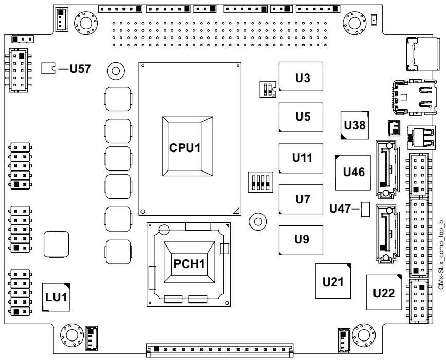
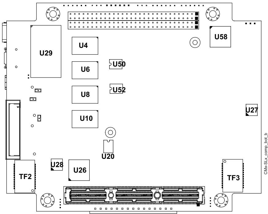
Table 2-1 describes the major ICs on the CMx-SLx, including a brief description of each IC. Figures 2-1 and 2-2 show the locations of the major ICs.

Table 2-1: Major Component Descriptions and Functions

<table><tr><td>Chip Type</td><td>Mfg.</td><td>Model</td><td>Description</td><td>Function</td></tr><tr><td>CPU (CPU1)</td><td>Intel</td><td>CoreTM i3-6102E, 1.9GHz (25W tuned to 17W)CoreTM i3-6100E, 2.7GHz (35W)Xeon® E3-1505L v5, 2.0GHz (25W)</td><td>Central Processing Unit with 2 execution cores and up to 3MB L2 cache</td><td>Integrates Processor Core and Graphics Memory Controller Hub</td></tr><tr><td>Gigabit Ethernet PHY Transceiver (LU1)</td><td>Intel</td><td>WGI219LM SLKJ3</td><td>Single-port Gigabit Ethernet PHYTransceiver for GLAN1 interface</td><td>Provides a standard IEEE 802.3 Ethernet interface for Ethernet transfer rates up to 1000 Mb/s</td></tr><tr><td>Chipset (PCH1)]</td><td>Intel</td><td>CM236</td><td>I/O Hub for common user interfaces</td><td>Provides Southbridge interfaces and off loads some Northbridge functions from the CPU</td></tr><tr><td>DDR4 SDRAM (U3, U5, U7, U9, [and U11 to enable ECC])</td><td>Micron Hynix</td><td>N/A</td><td>On-board DDR4, memory module</td><td>Provides high-speed data transfer</td></tr><tr><td>DDR4 SDRAM (U4, U6, U8, U10 - all on bottom side [see Figure 2-2])</td><td>Micron Hynix</td><td>N/A</td><td>On-board DDR4, memory module</td><td>Provides high-speed data transfer</td></tr><tr><td>Ethernet EEPROM (U20)</td><td>Winbond</td><td>W25Q16DVSSIG</td><td>Three-Wire Serial EEPROM for Gigabit Ethernet Controller</td><td>Provides storage for MAC addresses, serial numbers, and pre-boot configuration data</td></tr><tr><td>Gigabit Ethernet Controller (U21 on bottom side; see Figure 2-2)</td><td>Intel</td><td>WGI210IT SLJXT</td><td>Single-port Gigabit Ethernet controller for GLAN2 interface</td><td>Integrates GbEMAC, PHY, and SGMII/SerDes to enable 10T/100TX/1000TEthernet signals using the PCIe x1 bus</td></tr><tr><td>Embedded DisplayPort-to-LVDS Converter (U22)</td><td>NXP</td><td>PTN3460</td><td>Embedded DisplayPort (eDP) to LVDS bridge device that enables connectivity between an embedded DisplayPort (eDP) source and an LVDS display panel.</td><td>Processes the incoming embedded DisplayPort (eDP) stream, performs eDP to LVDS protocol conversion, and transmits processed stream in LVDS format.</td></tr><tr><td>LPC-to-UART Controller (U26)</td><td>Fintek</td><td>F81216AU-I</td><td>Serial communication controller</td><td>Provides 4 UART ports through the LPC bus</td></tr><tr><td>RS-232 Transceiver (U27)</td><td>Texas Instruments</td><td>TRS3253EIRSMR</td><td>Transceiver for Serial 1 RS-232 signals</td><td>Transmits and receives RS-232 signals for COM1</td></tr><tr><td>RS-232 Transceiver (U28)</td><td>Texas Instruments</td><td>TRS3253EIRSMR</td><td>Transceiver for Serial 2 RS-232 signals</td><td>Transmits and receives RS-232 signals for COM2</td></tr><tr><td>Solid State Drive [SSD] - SATA (U29) - on bottom side [see Figure 2-2])</td><td>Greenliant</td><td>8GB: GLS85LS1008P 32GB GLS85LS1032P</td><td>Industrial-grade soldered solid-state storage module</td><td>Provides solid state storage through SATA 6Gb/s port</td></tr><tr><td>HDMI Level Shifter (U38)</td><td>NXP</td><td>PTN3360DBS</td><td>HDMI level-shift IC for HDMI video</td><td>Converts HDMI differential input from the PCH to TMDS differential output for the HDMI interface</td></tr><tr><td>BMC (U46)</td><td>Texas Instruments</td><td>TM4C123BH6ZRBT7R</td><td>Microcontroller</td><td>Provides logistics and forensic information, flat panel control, I2C bus control, user flash, Watchdog Timer and fan control</td></tr><tr><td>Temperature Sensor - CPU (U47 on bottom side; see Figure 2-2)</td><td>Texas Instruments</td><td>LM73</td><td>Digital-output temperature sensor</td><td>Measures its own temperature and the temperature of the CPU thermal diode and provides temperature correction with fan speed control.</td></tr><tr><td>SPI Flash (U50 and U52)</td><td>Macronix</td><td>MX25L12835FM2I-10GRT</td><td>Serial Peripheral Interface Flash Memory chip (for firmware)</td><td>Stores BIOS 0 and BIOS 1 in Flash Memory</td></tr><tr><td>EEPROM, PCIe-to-PCI Bridge (U57 - on bottom side [see Figure 2-2])</td><td>Atmel</td><td>AT24C08D</td><td>Two-Wire Serial EEPROM for PCIe-to-PCI Bridge</td><td>Stores PCIe-to-PCI bridge configuration data</td></tr><tr><td>PCIe-to-PCI Bridge (U58)</td><td>Texas Instruments</td><td>XIO2001</td><td>PCIe-to-PCI interface</td><td>Migrates legacy PCI interfaces</td></tr><tr><td>Gb Ethernet Transformer (TF3 - on bottom side) [see Figure 2-2]</td><td>BOTHHAND</td><td>GST5009M</td><td>Gigabit Ethernet Magnetics</td><td>Provides electrical isolation for Gigabit Ethernet PHY transceiver (GLAN1)</td></tr><tr><td>Gb Ethernet Transformer (TF2 - on bottom side) [see Figure 2-2]</td><td>BOTHHAND</td><td>GST5009M</td><td>Gigabit Ethernet Magnetics</td><td>Provides electrical isolation for Gigabit Ethernet controller (GLAN2)</td></tr></table>

# Key:

CPU1 - CPU

LU1 - Ethernet PHY Transceiver

PCH1 - PCH

U3 - DDR4 SDRAM

U5 - DDR4 SDRAM

U7 - DDR4 SDRAM

U9 - DDR4 SDRAM

U11 - DDR4 SDRAM (ECC)

U21 - Gigabit Ethernet Controller

U22 - DisplayPort-to-LVDS Converter

U38 - HDMI Level Shifter

U46 - BMC

U47 - Temperature Sensor

U57 - PCIe-to-PCI Bridge EEPROM
![U57\nCPU1\nU3\nU5\nU38\nU11\nU46\nU7\nU47-\nU9\nPCH1\nLU1\nU21\nU22\nCMx-SLx_comp_top_b](.cmx-slx-50m-00063-1040-14/358cdd4c6c26e26a1c11948a0411fb208d30fe98618593a2a841e0e1d72bf8f0.jpg)

Figure 2-1: Component Locations (Top Side)

# Key:

U4 - DDR4 SDRAM

U6 - DDR4 SDRAM

U8 - DDR4 SDRAM

U10 - DDR4 SDRAM

U20 - Gigabit Ethernet EEPROM

U26 - LPC-to-UART Controller

U27 - RS-232 Transceiver (COM1)

U28 - RS-232 Transceiver (COM2)

U29 - SSD (Solid State Drive)

U50 - BIOS1

U52 - BIOS2

U58 - PCIe-to-PCI Bridge

TF2 - GbE 2 Transformer

TF3 - GbE 1 Transformer
![U29\nU4\nU6\nU50\nU8\nU52\nU10\nU27\nU28\nU26\nTF2\nTF3\nCMx-SLx_comp_bot_b](.cmx-slx-50m-00063-1040-14/caaf6a1bf01e69baf90f7871b73450679a3ebf6281976b7b0ea77661307e5529.jpg)

Figure 2-2: Component Locations (Bottom Side)

# 2.2 Header and Connector Definitions and Locations

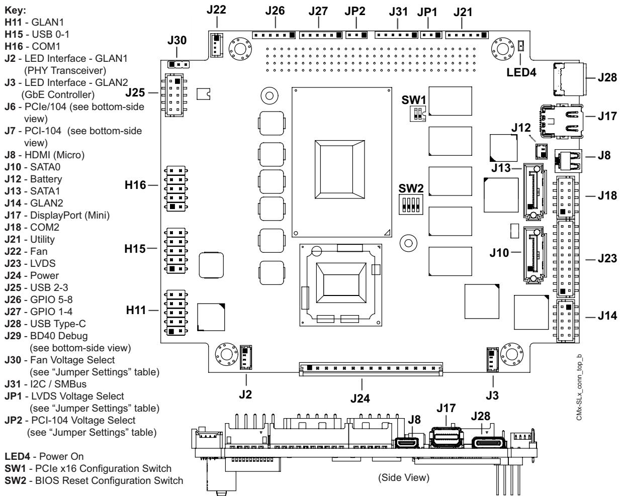
Table 2-2 describes the headers, connectors, and sockets shown in Figures 2-3 and 2-4.

Table 2-2: Header and Connector Descriptions

<table><tr><td>Header/Connector #</td><td>Access</td><td>Description</td></tr><tr><td>H11 – GLAN1</td><td>Top</td><td>10-pin, 0.100" (2.54mm) header for Gigabit Ethernet port 1 (JIH JVE, 21N22564-10M00B-01G-6-C-02)</td></tr><tr><td>H15 – USB (0-1)</td><td>Top</td><td>10-pin, 0.100" (2.54mm) header for USB 2.0 ports 0-1 (JIH JVE, 21N22564-10M00B-01G-6-C-02)</td></tr><tr><td>H16 – COM1</td><td>Top</td><td>10-pin, 0.100" (2.54mm) header for serial port 1 (JIH JVE, 21N22564-10M00B-01G-6-C-02)</td></tr><tr><td>J2 – LED - GLAN1</td><td>Top</td><td>4-pin, 0.049" (1.25mm) shrouded, single-row header for Gigabit Ethernet port 1 LED (REGO, 830-1251-02STD-3.2-6T)</td></tr><tr><td>J3 – LED - GLAN2</td><td>Top</td><td>4-pin, 0.049" (1.25mm) shrouded, single-row header for Gigabit Ethernet port 2 LED (REGO, 830-1251-02STD-3.2-6T)</td></tr><tr><td>J6 – PCIe/104</td><td>Bottom</td><td>156-pin, 0.025" (0.64mm) standard PCI Express connector for SMBus, USB 2.0, PCIe x1, and PCI interfaces (SAMTEC, ASP-129646-03)</td></tr><tr><td>J7 – PCI-104</td><td>Bottom</td><td>60-pin, 0.079" (2mm) standard PCI-104, male connector for PCI interfaces (EPT, 264-17302)</td></tr><tr><td>J8 – HDMI (Micro)</td><td>Top</td><td>19-pin, 0.016" (0.04mm), standard micro-connector for HDMI Type D video port (MOLEX, 46765-0001)</td></tr><tr><td>J10 – SATA0</td><td>Top</td><td>7-pin, 0.050" (1.27mm) standard connector for SATA 6Gb/s port 0 (WIN WIN, WATF-07DBLBA1UW)</td></tr><tr><td>J12 – Battery</td><td>Top</td><td>2-pin, 0.049" (1.25mm) shrouded header for power from external battery (REGO, 830-1251-02STD-3.2-6T)</td></tr><tr><td>J13 – SATA1</td><td>Top</td><td>7-pin, 0.050" (1.27mm) standard connector for SATA 6Gb/s port 1 (WIN WIN, WATF-07DBLBA1UW)</td></tr><tr><td>J14 – GLAN2</td><td>Top</td><td>10-pin, 0.079" (2mm) shrouded header for Gigabit Ethernet port 2 (CST, CSI-2221-102R)</td></tr><tr><td>J17 – DisplayPort (MIni)</td><td>Top</td><td>20-pin, right-angle Thunderbolt connector for Mini DisplayPort interface (FOXCONN, 3VT11207-N730-7H)</td></tr><tr><td>J18 – COM2</td><td>Top</td><td>10-pin, 0.079" (2mm) shrouded header for serial port 2 (CST, CSI-2221-102R)</td></tr><tr><td>J21 – Utility</td><td>Top</td><td>6-pin, 0.079" (2mm) single-row header for Power Button, Reset Switch, and Speaker (SAMTEC, TMM-106-03-L-S)</td></tr><tr><td>J22 – Fan</td><td>Top</td><td>4-pin, 0.049" (1.25mm) single-row, shrouded header for power to external fan (HIROSE, DF13-4P-1.25DSA)</td></tr><tr><td>J23 – LVDS</td><td>Top</td><td>20-pin, 0.079" (2mm) shrouded header for LVDS video port (CST, CSI-2221-202R)</td></tr><tr><td>J24 – Power</td><td>Top</td><td>15-pin, 0.100" (2.54mm) shrouded, straight header for supplying external power to the board (JST, B15B-EH-A/LF)</td></tr><tr><td>J25 – USB 2-3</td><td>Top</td><td>10-pin, 0.079" (2mm) shrouded header for USB 2.0 ports 2-3 (CST, CSI-2221-102R)</td></tr><tr><td>J26 – GPIO1, (ports 5-8)</td><td>Top</td><td>6-pin, 0.079" (2mm) single-row header for GPIO1, ports 5-8 (SAMTEC, TMM-106-03-L-S)</td></tr><tr><td>J27 – GPIO2 (ports 1-4)</td><td>Top</td><td>6-pin, 0.079" (2mm) single-row header for GPIO2, ports 1-4 (SAMTEC, TMM-106-03-L-S)</td></tr><tr><td>J28 – USB Type-C</td><td>Top</td><td>24-pin, standard female right-angle connector for USB 3.1 host function(FOXCONN, UT11113-11604-7)</td></tr><tr><td>J29 – DB40 Debug</td><td>Bottom</td><td>40-pin, DB40 Front-Flip connector for debug card (Molex, 502790-4091)</td></tr><tr><td>J30 – Fan Voltage Select (see Table 2-3 for settings)</td><td>Top</td><td>3-pin, 0.079" (2mm) single-row jumper header for setting the fan interface voltage(JIH21N1250-03S10B-01G-4/2.8-G)</td></tr><tr><td>J31 – I2C / SMBus</td><td>Top</td><td>6-pin, 0.079" (2mm) single-row header for I2C and SMBus interfaces(SAMTEC, TMM-106-03-L-S)</td></tr><tr><td>JP1 – LVDS Voltage Select</td><td>Top</td><td>3-pin, 0.079" (2mm) single-row jumper header for setting the LVDS interface voltage(JIH21N1250-03S10B-01G-4/2.8-G)</td></tr><tr><td>JP2 – PCI-104 Voltage Select</td><td>Top</td><td>3-pin, 0.079" (2mm) single-row jumper header for setting the PCI-104 interface voltage(JIH21N1250-03S10B-01G-4/2.8-G)</td></tr><tr><td>LED1 – BMC Status</td><td>Bottom</td><td>Indicates system-error blink codes (Blue)[LIGITEK, LG-192DBK-CT/T]</td></tr><tr><td>LED2 – +3V3 Standby Power On</td><td>Bottom</td><td>Indicates standby power on (Green)[LIGITEK, LG-192G-CT]</td></tr><tr><td>LED3 – Watchdog Status</td><td>Bottom</td><td>Indicates triggered watchdog timer (Red)[LIGITEK, LG-192HRF-CT]</td></tr><tr><td>LED4 – +5V Power On</td><td>Top</td><td>Indicates +5V power on (Green)[LIGITEK, LG-192G-CT]</td></tr><tr><td>SW1 – PCIe x16 Lane Configuration Switch</td><td>Top</td><td>2-pole dip switch for selecting CPU PCIe x16 lane configurations (WIN WIN, DHN-02-T-V-T/R)Switch PositionsLane Configurations1-OFF, 2-OFF = 1x16 [Default]1-OFF, 2-ON = 2x81-ON, 2-OFF = Reserved1-ON, 2-ON = 1x8, 2x4Switch Positions&lt;img src="images/740e6cc801f3396cb43c50444035c7cdf9f753e122e2090d024d5ad05ca78be5.jpg"/&gt;</td></tr><tr><td>SW2 - BIOS ResetConfiguration Switch</td><td>Top</td><td>4-pole dip switch for configuring BIOS reset(DIPTRONICS, DHNF-04-T-Q-T/R)Pole 1 - CPU_BIOS_Default► OFF= User settings active [default]► ON = Resets BIOS user settingsPole 2 - BIO_Mode► OFF = Failsafe BIOS [default]► ON = Normal BIOSPole 3 - SEL_BIOS► OFF = BIOS 1 active► ON = BIOS 0 active [default]Pole 4 - POSTWDT_DIS#► OFF = Watchdog timer disabled [default]► ON = Watchdog timer active&lt;img src="images/580c30e51c037f4c9e8dba6754b6b247820c35ff2ec962b82bf1854e53562833.jpg"/&gt;</td></tr></table>

![Key:\nH11 - GLAN1\nH15 - USB 0-1\nH16 - COM1\nJ2 - LED Interface - GLAN1\n(PHY Transceiver)\nJ3 - LED Interface - GLAN2\n(GbE Controller)\nJ6 - PCIe/104 (see bottom-side\nview)\nJ7 - PCI-104 (see bottom-side\nview)\nJ8 - HDMI (Micro)\nJ10 - SATA0\nJ12 - Battery\nJ13 - SATA1\nJ14 - GLAN2\nJ17 - DisplayPort (Mini)\nJ18 - COM2\nJ21 - Utility\nJ22 - Fan\nJ23 - LVDS\nJ24 - Power\nJ25 - USB 2-3\nJ26 - GPIO 5-8\nJ27 - GPIO 1-4\nJ28 - USB Type-C\nJ29 - BD40 Debug\n(see bottom-side view)\nJ30 - Fan Voltage Select\n(see 'Jumper Settings' table)\nJ31 - I2C / SMBus\nJP1 - LVDS Voltage Select\n(see 'Jumper Settings' table)\nJP2 - PCI-104 Voltage Select\n(see 'Jumper Settings' table)\nLED4 - Power On\nSW1 - PCIe x16 Configuration Switch\nSW2 - BIOS Reset Configuration Switch\nJ22 J26 J27 JP2 J31 JP1 J21 J30 J24 J3 J8 J17 J28\nLED4 - Power On\nCMx-SLx_comm_top_b\n(Side View)](.cmx-slx-50m-00063-1040-14/0421d4515e75ea252093e2ba9711efc0dd4cc90cedb042b03b3ceedc18501624.jpg)

Figure 2-3: Header and Connector Locations (Top Side)
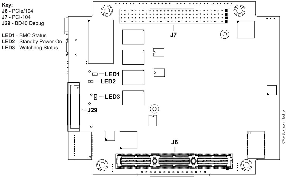
![Key:\nJ6 - PCIe/104\nJ7 - PCI-104\nJ29 - BD40 Debug\nLED1 - BMC Status\nLED2 - Standby Power On\nLED3 - Watchdog Status\nJ7\nLED1\nLED2\nLED3\nJ29\nJ6\nCMx-SLx corn_bot_b](.cmx-slx-50m-00063-1040-14/d4d77386a3ab0a79a22e65e1fd0f7b7095c2dbe5a52dd0e4edb5678dd046c03b.jpg)

Figure 2-4: Header and Connector Locations (Bottom Side)

![This image displays a white document icon featuring a large, bold red checkmark overlaid in the center. Faint grey horizontal lines are visible on the right side of the paper, simulating text, and the icon has a slightly glossy or glass-like appearance.](.cmx-slx-50m-00063-1040-14/44e7a352aed98a1d56c24166ad4afdb4bebbf98f2f5ebc4ee0bf9129e2f689a7.jpg)
NOTE:

Pin 1 is shown as a larger, black square on headers and connectors.

# 2.3 Jumper Header Definitions

Table 2-3 describes the jumper headers shown in Figure 2-5. All jumper headers provide 0.079" (2mm) pitch.

Table 2-3: Jumper Settings

<table><tr><td>Jumper Header</td><td>Jumper on Pins 1-2</td><td>Jumper on Pins 2-3</td></tr><tr><td>J30 – Fan Voltage</td><td>Enable +5V (1-2)</td><td>Enable +12V (2-3)(Default)</td></tr><tr><td>JP1 – LVDS Voltage Selection(JIH JVE, 27S1001-OPS35-01G-B)</td><td>Enable +3.3V (1-2) (Default)</td><td>Enable +5V (2-3)</td></tr><tr><td>JP2 – PCI-104 Voltage Selection(JIH JVE, 27S1001-OPS35-01G-B)</td><td>Enable +3.3V (1-2) (Default)</td><td>Enable +5V (2-3)</td></tr></table>

Note: Remove all jumpers to set 18-bit LCD interface.

![Key:\nJ30 - Fan Voltage Select\nJP1 - LVDS Voltage Select\nJP2 - PCI-104 Voltage Select](.cmx-slx-50m-00063-1040-14/de09f0db7c7e8df3d84b42f62aadd58be73af3ddc7e2c9ae71a25af76702bf36.jpg)

Figure 2-5: Jumper Header Locations (Top Side)

# 2.4 Component Features

This section further describes the supported features of the CMx-SLx major, on-board hardware components.

# 2.4.1 CPU

The CMx-SLx features the 6th Generation Intel® Core™ i3 and Intel® Xeon® E3 processor. The CPU integrates a high-performance 64-bit, x86 Processor Core with Memory Controller and GEN 9 graphics engine. This single chip—based on Intel 64 Architecture and built on 14-nm process technology—provides two execution cores and a Gen 3 Direct Media Interface (DMI) for high-speed connectivity to the Chipset. The CPU also supports Intel Hyper-Threading Technology and up to 16GB of DDR4 SDRAM memory at 1866MHz for high overall performance. Refer to the 6th Generation Intel Processor Data Sheet for H-Platforms on the Intel website for more information.

# 2.4.4 Chipset

The Intel® CM236 Chipset functions as the IO hub, controlling the DMI and system clock on the CPU and delivering IO interfaces at transfer rates of 8 GT/s. The CM236 supports Gen 3 PCIe connectivity with new technologies such as Intel Rapid Storage Technology 14, Context Sensing SDK, and Platform Trust Technology 3.0. Refer to the CM236 data sheet at the Intel website.

# 2.4.2 SDRAM

The CMx-SLx employs one 1866/2133MHz memory channel with one rank of eight system memory chips (and one additional chip for ECC). The board provides up to 16GB of extended memory using 16Gb DDR4 SDRAM chips. The CPU features Intel FMA (Fast Memory Access) technology, providing Just-in-Time Scheduling for issuing concurrent requests, Command Overlap for issuing multiple overlapping commands, and Out-of-Order Scheduling to re-order requests made to the same open page.

# 2.4.5 Gigabit Ethernet PHY Transceiver (I219 - Supporting GLAN1)

The Intel I219 provides a dedicated Physical Layer (PHY) interconnect between the Media Access Controller (MAC) on the Chipset and the first Gb Ethernet interface (GLAN1) on the CMx-SLx. The PHY circuitry provides a standard IEEE 802.3 Ethernet interface for 10BASE-T, 100BASE-TX, and 1000BASE-T applications (802.3, 802.3U, and 802.3ab). The I219 allows for less power consumption during periods of low data activity with the support for the Energy Efficient Ethernet (EEE) 802.az specification. Communication between the I219 and the Chipset occurs through PCIe and SMBus interfaces. The PCIe interface is used for all link speeds when the system is in an active state, and the SMBus interface is used only when the system is in a low power state. For remote, out-of-band system management, the I219 supports Intel Active Management Technology (AMT) 11.0. Refer to the Intel Ethernet Connection I219 data sheet on the Intel web site for more information.

# 2.4.6 Gigabit Ethernet Controller (I210 - Supporting GLAN2)

The second Gb Ethernet interface (GLAN2) originates from the Intel I210 Controller, which provides a single-port controller that supports GbE functionality using the high-speed PCIe standard, v2.1 (2.5GT/s). The I210 features a fully-integrated Media Access Control (MAC) and a Physical Layer (PHY), which enable 1000BASE-T implementations such as rack-mounted or pedestal servers in add-on NIC or LAN-on-Motherboard (LOM) designs. Other implementations include blade servers such as LOMs or mezzanine cards as well as embedded applications such as switch add-on cards and network appliances. Additionally, the I210 integrates an SGMII/SerDes port, which allows MAC-to-MAC blade server connections or MAC-to-external PHY connections. Refer to the Intel I210 Ethernet Controller data sheet on the Intel web site.

# 2.4.7 SSD (Solid State Drive)

The CMx-SLx provides an on-board, 8GB SSD for user storage. The SSD communicates with the Chipset through the SATA 3Gb/s port and is user-accessible through the BIOS Boot menu and the OS interface. For more information, refer to the GLS85LS1008P/GLS85LS1032P SSD data sheet on the Greenliant website.

# 2.4.3 BMC

The Board Management Controller (BMC) is a micro-controller chip that transmits and receives data to and from the SEMA, BIOS, and debug utilities—monitoring system performance, behavior, and diagnostics at transfer speeds up to 3.33Mbps at 400KHz. The BMC queries components on the board for data related to temperature, power-supply voltage and current, power sequencing, logistics and forensics, flat panel control, I2C bus control, user flash, Watchdog Timer, and fan control. Refer to the Texas Instruments web site for more information on the TM4C123GH6ZRB micro-controller.

# 2.4.4 LM73 Temperature Sensor

The temperature sensor operates over a wide temperature range (-40°C to +150°C) with a 14-bit mode maximum resolution. Programmed to the BMC and controlled through the SEMA user interface, the temperature sensor monitors system temperatures and issues alerts, time outs, resets, and shutdowns, protecting the system as it approaches temperature limits. For more information on the LM73 Temperature Sensor, refer to the data sheet on the Texas Instruments website.

# 2.4.5 PTN3460I eDP-to-LVDS Converter

The PTN3460I supports single-bus or dual-bus LVDS signalling with color depths of 18 bits per pixel or 24 bits per pixel and pixel clock frequency up to 112MHz. LVDS data packing can be done either in VESA or JEIDA formats. Also, the DP AUX interface transports I2C-over-AUX commands and supports EDID-DDC communication with an LVDS panel. To support panels without EDID ROM, the PTN3460 can emulate EDID ROM behavior, avoiding specific changes in system video BIOS. Find more details on the NXP website.

# 2.4.6 SMBus Slave Addresses

Table 2-8 lists the corresponding slave addresses of the devices on the SMBus.

Table 2-8: SMBus Slave Addresses

<table><tr><td>Address (HEX)</td><td>Function</td><td>Device</td></tr><tr><td>(50)</td><td>BIOS / SEMA</td><td>BMC</td></tr><tr><td>(92)</td><td>Temperature Sensor</td><td>LM73</td></tr><tr><td>(C0)</td><td>eDP-to-LVDS Converter</td><td>PTN3460I</td></tr><tr><td>(C8)</td><td>GbE PHY</td><td>I219</td></tr><tr><td>APR</td><td>PCIe Connector</td><td>PCIe Connector</td></tr></table>

# 2.5 Standard Connectors

The section describes the industry-standard connectors on the board.

# 2.5.1 Micro HDMI (J8)

The Micro HDMI connector (J8) provides the standard interface for IO connection to and from an HDMI audiovisual device. Figure 2-6 provides schematic and mechanical presentations of the micro HDMI connector.

![The image displays a standard safety warning sign featuring a yellow triangle with a black border and a black exclamation point in the center. Below the triangle, the word 'CAUTION:' is printed in bold, black capital letters.](.cmx-slx-50m-00063-1040-14/fda92713c0b00b357f522a5e2008a5dac5111a4cd0abb411a859f567901d1a42.jpg)
MISE EN GARDE

Make sure the width of the mating connector does not conflict with the width of the mini DisplayPort mating connector.

Assurez-vous que la largeur du connecteur correspondant n'est pas en conflit avec la largeur du connecteur correspondant mini DisplayPort.

![MYLAR\n3.60±0.1\n0.40±0.05\n0.16±0.03\n7.50\n3.00\n6.50](.cmx-slx-50m-00063-1040-14/9add2e92902a8f9b5d2c7bd4d9130e73e94296890a2845ba8f067ae166798a44.jpg)

![5.90±0.03\n#19\n#1\n#18\n6.20\n#2\n2.30±0.03](.cmx-slx-50m-00063-1040-14/355a1a6b5089e5f263fdd6a4aee391959ba33360724a69cb7ceb6883c2ae1b54.jpg)

![P +5V_S_HDMI\n500mA\nJ8\nSHELL4\n23\nHPD\n+5V\nSHELL3\n22\nTMDS P0 HPD\n19\nNC\n18\nDDC SDA\n17\nDDC SCL\n16\nCEC\n15\nGND\n14\nCK-\n12\nCK+\n13\nCK Shield\n11\nD0-\n9\nD0+\n10\nD0 Shield\n8\nD1-\n6\nD1+\n7\nD1 Shield\n5\nD2-\n3\nD2+\n4\nSHELL2\n21\nSHELL1\n20\nHDMI-19P\nR671 0ohm ←1%\nR0603 0ohm ←1%\nR670 R0603\nHDMI_GND](.cmx-slx-50m-00063-1040-14/7dcf90b531169173f50039e2a03cc70d3610a4e741b525c80546c8465da6ac10.jpg)

Figure 2-6: Micro HDMI connector

# 2.5.2 Mini DisplayPort (J17)

The Mini DisplayPort connector (J17) provides the standard interface to drive IO connection to and from a DisplayPort audiovisual device. Figure 2-7 provides schematic and mechanical presentations of the Mini DisplayPort connector.

![A yellow triangular warning sign with a black border featuring a black exclamation point in the center.](.cmx-slx-50m-00063-1040-14/b8ab3c92cf0d870cb18c930663b07f232aff42cf9f442d700cc44dd8fe13e035.jpg)
CAUTION:
MISE EN GARDE

Make sure the width of the mating connector does not conflict with the widths of the micro HDMI and USB Type-C mating connectors.

Assurez-vous que la largeur du connecteur d'accouplement n'est pas en conflit avec les largeurs des connecteurs d'accouplement micro HDMI et USB Type-C.

![J17\nG_MINIDP_HPD\n1\n2\nPWR_IN\nHPD_GND\n3\n4\nTBT_HD2CA_0+\nTBT_CA2HD_0+\nTBT_HD2CA_0-\nTBT_CA2HD_0-\nGND1\nGND2\nG_MINIDP_TX1_P\n9\nLSTX\nRESERVED1\nLSRX\nRESERVED2\nGND3\nGND4\nG_MINIDP_TX3_P\n10\nTBT_HD2CA_1+\nTBT_CA2HD_1+\nTBT_HD2CA_1-\nTBT_CA2HD_1-\nRETURN\nPWR_OUT\nThunderbolt_20\nN1\nN2\nG1\nG2\nG3\nG4\nP_+3V3_S_MINIDP\n55mA\nGND\nDP_GND\nR655 0ohm +-1%\nR0603\nG656 0ohm +-1%\nR0603\nDP_GND\nP_+3V3_S\nP_+3V3_S_MINIDP\nA D14 K\nNSR0320MW2T1G_20V](.cmx-slx-50m-00063-1040-14/dfc4bba27b1c731e7d7c26b2fd3a34e3f365175dca9f0d30af81e5e68c5ed07b.jpg)

Figure 2-7: Mini DisplayPort connector

# 2.5.3 USB Type-C (J28)

The USB Type-C connector (J28) provides a standard USB Type-C interface for super-speed USB 3.1 host and device signals. Figure 2-8 provides schematic and mechanical presentations of the USB Type-C connector.

![The image displays a standard safety warning sign featuring a yellow triangle with a black border. Inside the triangle is a black exclamation point. Below the triangle, the word 'CAUTION:' is written in bold, black capital letters.](.cmx-slx-50m-00063-1040-14/aee95f6438f374faaa277eed03879934f78f563d54a8e89de80045aab45d1ba8.jpg)
MISE EN GARDE

Make sure the width of the mating connector does not conflict with the width of the mini DisplayPort mating connector.

Assurez-vous que la largeur du connecteur correspondant n'est pas en conflit avec la largeur du connecteur correspondant mini DisplayPort.

USB
TYPE C
![A1\nA12\nB12\nB1](.cmx-slx-50m-00063-1040-14/f0f120a6e6c1afa364ad5f7c6f79c0a085b7f834af4598c8e891708f571d69fd.jpg)

![P_+5V_USB8\nCN_U3_P1_TXP\nCN_U3_P1_TXN\nCN_U2_P1_DP\nCN_U2_P1_DN\nCN_U3_P2_RXP\nCN_U3_P2_RXN\nA2\nA4\nA3\nA6\nA1\nA7\nA11\nA12\nA10\nJ28A\nSSTXP1\nVBUS1\nCC1\nSSTXN1\nRFU1\nDP1\nGND1\nDN1\nSSRXP2\nGND2\nSSRXN2\n1 OF 3\nUSB_24_Type C\nP_+5V_USB8\nCN_U3_CC1\nA9\nA5\nA8\nP_+5V_USB8\nP_+5V_USB8\nCN_U3_P2_TXP\nCN_U3_P2_TXN\nCN_U2_P1_DP\nCN_U2_P1_DN\nCN_U3_P1_RXP\nCN_U3_P1_RXN\nB2\nB4\nB3\nB6\nB1\nB7\nB11\nB12\nB10\nJ28B\nSSTXP2\nVBUS4\nCC2\nSSTXN2\nRFU2\nDP2\nGND3\nDN2\nSSRXP1\nGND4\nSSRXN1\n2 OF 3\nUSB_24_TYPE C](.cmx-slx-50m-00063-1040-14/294141420352daa493fc56ac201f4a60f76954574469dc3849dcbd97ab77de0a.jpg)

![J28_C\nG1 G1 G5\nG2 G2 G6\nG3 G3 G7\nG4 G4\nN1 N1\nN2 N2\nJ28_GND\nR669 R668\n0ohm +1%\nR0603\n0ohm +1%\nR0603\n1 p in G5\n1 p in G6\n1 p in G7\n1 p in G8\nG9 G10\nUSB_24_Type C\n3 OF 3\nJ28_GND](.cmx-slx-50m-00063-1040-14/ef979c580c510201a79621049cb3f4ee613d33906df3a7612699f371a04b28b0.jpg)

![P_+5V_USB8\nR511\n22K_+-1%\nR512\n22K_+-1%\nCN_U3_CC1\nCN_U3_CC2](.cmx-slx-50m-00063-1040-14/935a23cad4d2412a82c40c825157e89ba7a8ead87ef76151c838d085cc387a6e.jpg)

Figure 2-8: USB Type-C connector

# 3 Interfaces

This chapter provides descriptions and signal definitions only of the non-standard interfaces on the board. Descriptions and signal definitions of standard interfaces such as PCI-104 and SATA can be found in their respective specification data sheets. If certain signals of standard interfaces have been modified or disconnected, those interfaces will be described in this chapter.

![An icon depicting a white document with a folded top-right corner and faint horizontal lines. A large, bold red checkmark is superimposed over the center of the document. Below the graphic is the text 'NOTE:'.](.cmx-slx-50m-00063-1040-14/7d0454dc9884a496122a84bcd6325cefcda264ef1d70a5c70c505feca77c9876.jpg)

The tables in this chapter define pin sequence using the method in the following example: A 10-pin header with two rows of pins, using odd/even numbering, where pin 2 is directly across from pin 1, is noted as 10 pins, 2 rows, odd/even pin sequence (1, 2). Consecutive numbering is noted, for example, as 24 pins, 2 rows, consecutive pin sequence (1, 13), where pin 13 is directly across from pin 1. Refer to Figure 2-3 and Figure 2-4 for pin-1 locations.

# 3.1 Serial Interfaces (H16 and J18)

Table 3-1 provides the signals for serial port 1 interface. Table 3-2 provides the signals for serial port 2 interface. Serial port 1 uses a 10-pin, vertical header with 2 rows, odd/even sequence (1, 2), and 0.100" (2.54mm) pitch. Serial port 2 uses a 10-pin, vertical header with 2 rows, odd/even sequence (1, 2), and 0.079" (2.00mm) pitch.

Note: The shaded table cell denotes ground. The # symbol indicates the signal is Active Low.
Table 3-1: Serial Port 1 (COM1) Signals (H16)

<table><tr><td>Pin #</td><td>Signal</td><td>DB9 #</td><td>Description</td></tr><tr><td>1</td><td>S1_DSR#</td><td>6</td><td>COM1 Data Set Ready – Indicates external serial device is powered, initialized, and ready. Used as hardware handshake with DTR for overall readiness.</td></tr><tr><td>2</td><td>S1_DCD#</td><td>1</td><td>COM1 Data Carrier Detect – Indicates external serial device is detecting a carrier signal (i.e., a communication channel is currently open). In direct connect environments, this input is driven by DTR as part of the DTR/DSR handshake.</td></tr><tr><td>3</td><td>S1_RTS#</td><td>7</td><td>COM1 Request To Send – Indicates serial port is ready to transmit data. Used as hardware handshake with CTS for low level flow control.</td></tr><tr><td>4</td><td>S1_RXD</td><td>2</td><td>COM1 Receive Data – Serial port receive data input is typically held at a logic 1 (mark) when no data is being transmitted, and is held “Off” for a brief interval after an “On” to “Off” transition on the RTS line to allow the transmission to complete.</td></tr><tr><td>5</td><td>S1_CTS#</td><td>8</td><td>COM1 Clear To Send – Indicates external serial device is ready to receive data. Used as hardware handshake with RTS for low level flow control.</td></tr><tr><td>6</td><td>S1_TXD</td><td>3</td><td>COM1 Transmit Data – Serial port transmit data output is typically held to a logic 1 when no data is being sent. Typically, a logic 0 (On) must be present on RTS, CTS, DSR, and DTR before data can be transmitted on this line.</td></tr><tr><td>7</td><td>S1_RI#</td><td>9</td><td>COM1 Ring Indicator – Indicates external serial device is detecting a ring condition. Used by software to initiate operations to answer and open the communications channel.</td></tr><tr><td>8</td><td>S1_DTR#</td><td>4</td><td>COM1 Data Terminal Ready – Indicates serial port is powered, initialized, and ready. Used as hardware handshake with DSR for overall readiness.</td></tr><tr><td>9</td><td>COMPORT_RST#</td><td></td><td>COM1 reset</td></tr><tr><td>10</td><td>GND</td><td>10</td><td>COM1 Ground</td></tr></table>

Table 3-2: Serial Port 2 (COM2) Signal (J18)

<table><tr><td>Pin #</td><td>Signal</td><td>DB9 #</td><td>Description</td></tr><tr><td>1</td><td>GND</td><td>10</td><td>COM2 Ground</td></tr><tr><td>2</td><td>GND</td><td>5</td><td>COM2 Ground</td></tr><tr><td>3</td><td>S2_DTR#</td><td>4</td><td>COM2 Data Terminal Ready – Indicates serial port is powered, initialized, and ready. Used as hardware handshake with DSR for overall readiness.</td></tr><tr><td>4</td><td>S2_RI#</td><td>9</td><td>COM2 Ring Indicator – Indicates external serial device is detecting a ring condition. Used by software to initiate operations to answer and open the communications channel.</td></tr><tr><td>5</td><td>S2_TXD</td><td>3</td><td>COM2 Transmit Data – Serial port transmit data output is typically held to a logic 1 when no data is being sent. Typically, a logic 0 (On) must be present on RTS, CTS, DSR, and DTR before data can be transmitted on this line.</td></tr><tr><td>6</td><td>S2_CTS#</td><td>8</td><td>COM2 Clear To Send – Indicates external serial device is ready to receive data. Used as hardware handshake with RTS for low level flow control.</td></tr><tr><td>7</td><td>S2_RXD</td><td>2</td><td>COM2 Receive Data – Serial port receive data input is typically held at a logic 1 (mark) when no data is being transmitted, and is held “Off” for a brief interval after an “On” to “Off” transition on the RTS line to allow the transmission to complete.</td></tr><tr><td>8</td><td>S2_RTS#</td><td>7</td><td>COM2 Request To Send – Indicates serial port is ready to transmit data. Used as hardware handshake with CTS for low level flow control.</td></tr><tr><td>9</td><td>S2_DCD#</td><td>1</td><td>COM2 Data Carrier Detect – Indicates external serial device is detecting a carrier signal (i.e., a communication channel is currently open). In direct connect environments, this input is driven by DTR as part of the DTR/DSR handshake.</td></tr><tr><td>10</td><td>S2_DSR#</td><td>6</td><td>COM2 Data Set Ready – Indicates external serial device is powered, initialized, and ready. Used as hardware handshake with DTR for overall readiness.</td></tr></table>

Note: The shaded table cells denote ground. The # symbol indicates the signal is Active Low.

# 3.2 USB 2.0 Interface (H15 and J25)

The CMx-SLx contains two root USB hubs and six functional USB ports. Four of the six USB ports are routed through two 10-pin headers (H15 and J25), and the other two ports are routed through the PCIe/104 interface connector. The PCH provides the USB function including the following features:

▶ Supports USB v.2.0 EHCI and USB v.1.1 UHCI
▶ Provides over-current detection status
- Provides a fuse on board for over-current protection

![The image features a white document icon with a folded upper right corner, overlaid with a large, green checkmark.](.cmx-slx-50m-00063-1040-14/735e441d2ecce23e57bc54088363090af1ba6f637e46df3ddcaddcb6c1f35cd4.jpg)
NOTE:

The standard USB 3.1 host interface is described in the USB Type-C (J28) section of Chapter 2.

Table 3-3 describes the pin signals of the USB0 and USB1 header which consists of 10 pins, in two rows, with odd/even (1, 2) pin sequence, and 0.100" (2.54mm) pitch.

Table 3-3: USB0 and USB1 Interface Pin Signals (H15)

<table><tr><td>Pin #</td><td>Signal</td><td>Description</td></tr><tr><td>1</td><td>USB-PWR_1</td><td>USB1 Power – VCC (+5V +/-5%) power goes to the port through an on-board fuse. Port is disabled if this input is low.</td></tr><tr><td>2</td><td>USB-PWR_0</td><td>USB0 Power – VCC (+5V +/-5%) power goes to the port through an on-board fuse. Port is disabled if this input is low.</td></tr><tr><td>3</td><td>CONN_USB1_N</td><td>USB1 Port Data Negative</td></tr><tr><td>4</td><td>CONN_USB0_N</td><td>USB0 Port Data Negative</td></tr><tr><td>5</td><td>CONN_USB1_P</td><td>USB1 Port Data Positive</td></tr><tr><td>6</td><td>CONN_USB0_P</td><td>USB0 Port Data Positive</td></tr><tr><td>7</td><td>USB_GND1</td><td>USB1 Ground</td></tr><tr><td>8</td><td>USB_GND0</td><td>USB0 Ground</td></tr><tr><td>9</td><td>USB_GND1</td><td>USB1 Ground</td></tr><tr><td>10</td><td>USB_GND0</td><td>USB0 Ground</td></tr></table>

Note: The shaded table cells denote power or ground.

Table 3-4 describes the pin signals of the USB2 and USB3 header, which consists of 10 pins in two rows, with odd/even (1, 2) pin sequence, and 0.079" (2mm) pitch.

Table 3-4: USB2 and USB3 Interface Pin Signals (J25)

<table><tr><td>Pin #</td><td>Signal</td><td>Description</td></tr><tr><td>1</td><td>USB_GND2</td><td>USB2 Ground</td></tr><tr><td>2</td><td>USB_GND3</td><td>USB3 Ground</td></tr><tr><td>3</td><td>USB_GND2</td><td>USB2 Ground</td></tr><tr><td>4</td><td>USB_GND3</td><td>USB3 Ground</td></tr><tr><td>5</td><td>CONN_USB2_P</td><td>USB2 Port Data Positive</td></tr><tr><td>6</td><td>CONN_USB3_P</td><td>USB3 Port Data Positive</td></tr><tr><td>7</td><td>CONN_USB2_N</td><td>USB2 Port Data Negative</td></tr><tr><td>8</td><td>CONN_USB3_N</td><td>USB3 Port Data Negative</td></tr><tr><td>9</td><td>USB-PWR_2</td><td>USB2 Power – VCC (+5V +/-5%) power goes to the port through an on-board fuse. Port is disabled if this input is low.</td></tr><tr><td>10</td><td>USB-PWR_3</td><td>USB3 Power – VCC (+5V +/-5%) power goes to the port through an on-board fuse. Port is disabled if this input is low.</td></tr></table>

Note: The shaded table cells denote power or ground.

# 3.3 Ethernet (H11 and J14)

The CMx-SLx supports two Gigabit Ethernet interfaces. The first Ethernet interface originates from the WGI219LM PHY transceiver, which occupies one PCI Express lane and supports the internal MAC (Media Access Controller) in the PCH. The second Ethernet interface is implemented through the WGI210AT Ethernet controller, which occupies one PCI Express lane and generates its own Gigabit Ethernet signals. The Ethernet function supports multi-speed operation at 10/100/1000 Mbps and operates in full-duplex at all supported speeds or half duplex at 10/100 Mbps while adhering to the IEEE 802.3x flow control specification. The Ethernet interface offers the following features:

▶ Full duplex support at 10 Mbps, 100 Mbps, or 1000 Mbps
▶ Half duplex support at 10 Mbps and 100 Mbps
▶ In full duplex mode, the Ethernet controller adheres to the IEEE 802.3x Flow Control specification
In half duplex mode, performance is enhanced by a proprietary collision reduction mechanism
▶ IEEE 802.3 compatible physical layer to wire transformer
▶ IEEE 802.3u Auto-Negotiation support
▶ Fast back-to-back transmission support with minimum interframe spacing (IFS)
▶ IEEE 802.3x auto-negotiation support for speed and duplex operation
▶ On-board magnetics (Ethernet isolation transformers)
Intel Active Management Technology (AMT) 11.0 support

Table 3-5 describes the pin signals of the Ethernet GLAN1 interface, which consists of a two-row, 10-pin vertical header with odd/even (1,2) pin sequence, and 0.100" (2.54mm) pitch.
Table 3-5: GLAN1 Interface Signal Descriptions (H11)

<table><tr><td>Pin #</td><td>Signal</td><td>Description</td></tr><tr><td>1</td><td>MDI1-</td><td rowspan="2">Media Dependent Interface 1 +/-</td></tr><tr><td>2</td><td>MDI1+</td></tr><tr><td>3</td><td>MDI2-</td><td rowspan="2">Media Dependent Interface 2 +/-</td></tr><tr><td>4</td><td>MDI2+</td></tr><tr><td>5</td><td>MDI0-</td><td rowspan="2">Media Dependent Interface 0 +/-</td></tr><tr><td>6</td><td>MDI0+</td></tr><tr><td>7</td><td>MDI3-</td><td rowspan="2">Media Dependent Interface 3 +/-</td></tr><tr><td>8</td><td>MDI3+</td></tr><tr><td>9</td><td>GND</td><td rowspan="2">Ground</td></tr><tr><td>10</td><td>GND</td></tr></table>

Note: The shaded table cells denote ground. The magnetics (isolation transformer, TF3) for the Ethernet connector is included on the CMx-SLx.

Table 3-6 describes the pin signals of the Ethernet GLAN2 interface, which consists of a two-row, 10-pin vertical header with odd/even (1,2) pin sequence, and 0.079" (2mm) pitch.

Table 3-6: GLAN2 Interface Signal Descriptions (J14)

<table><tr><td>Pin #</td><td>Signal</td><td>Description</td></tr><tr><td>1</td><td>GND</td><td rowspan="2">Ground</td></tr><tr><td>2</td><td>GND</td></tr><tr><td>3</td><td>MDI3+</td><td rowspan="2">Media Dependent Interface 3 +/-</td></tr><tr><td>4</td><td>MDI3-</td></tr><tr><td>5</td><td>MDI0+</td><td rowspan="2">Media Dependent Interface 0 +/-</td></tr><tr><td>6</td><td>MDI0-</td></tr><tr><td>7</td><td>MDI2+</td><td rowspan="2">Media Dependent Interface 2 +/-</td></tr><tr><td>8</td><td>MDI2-</td></tr><tr><td>9</td><td>MDI1+</td><td rowspan="2">Media Dependent Interface 1 +/-</td></tr><tr><td>10</td><td>MDI1-</td></tr></table>

Note: The shaded table cells denote ground. The magnetics (isolation transformer, TF2) for the Ethernet connector is included on the CMx-SLx.

# 3.4 Video (J8 [Micro HDMI], J17 [Mini DisplayPort], and J23 [LVDS])

The Core i3-6102E CPU provides an integrated 2D/3D graphics engine, which supports video decode such as MPEG2, VC-1, and AVC/H.264 (main, baseline at L3 and High-profile level 4.0/4.1) as well as video encode such as MPEG2, AVC/H.264 (baseline at L3), and VGA. The CPU supports LVDS, DisplayPort, and HDMI display ports, permitting simultaneous, independent operation of two displays. The CPU provides PCIe x16 Graphics signals to the PCIe/104 connector for an external high-performance PCI Express Graphics card or other general purpose PCI Express devices. The video interface features are listed in the following bullets. Refer to Table 3-7 for the LVDS signal definitions. The HDMI and DisplayPort interfaces are standard connectors, and those signals are defined in Chapter 2. The PEG signals are part of the standard PCIe/104 interface and are not defined in this manual.

# Mini DisplayPort:

▶ Supports resolutions of up to 4096x2304 @ 60 Hz
▶ Provides Main, Auxiliary, and Hot-Plug Detect signals
▶ Supports DisplayPort 1.2 specification
▶ Supports two DisplayPort interfaces

# LVDS:

▶ Supports a maximum resolution of 1400x1050 at 60Hz (pixel clock rate up to 112MHz)
▶ Supports minimum pixel clock rate of 25MHz
▶ Supports a single channel interface through a 20-pin header
▶ Supports pixel color depths of 18 and 24 bits

# Micro HDMI:

▶ Supports resolutions up to 3840x2160 pixels at 30Hz
▶ Supports pixel clock rates from 25MHz to 340MHz
▶ Supports DVD-Audio and Audio Return channel
▶ Provides one 19-pin, standard HDMI micro connector

# PEG (PCI Express Graphics):

▶ Supports external high-performance PCI Express graphics cards
▶ Supports general-purpose PCI Express devices
▶ Supports theoretical bandwidth of up to 8GT/s
▶ Provides PCIe Gen3 compliance

Table 3-7 lists the pin signals of the LVDS video header, which provides 20 pins, 2 rows, odd/even pin sequence (1, 2) with 0.079" (2mm) pitch.
Table 3-7: LVDS Video Interface Pin Signals (J23)

<table><tr><td>Pin #</td><td>Signal</td><td>Description</td></tr><tr><td>1</td><td>+12V_ATX</td><td>+12 volts for flat panel and backlight</td></tr><tr><td>2</td><td>VCC_LVDS_CONN</td><td>JP3 determines LVDS voltage (+3.3V or +5V)</td></tr><tr><td>3</td><td>GND</td><td>Ground</td></tr><tr><td>4</td><td>GND</td><td>Ground</td></tr><tr><td>5</td><td>LVDSA_CLK_P</td><td>LVDS A Clock Positive</td></tr><tr><td>6</td><td>LVDSA_CLK_N</td><td>LVDS A Clock Negative</td></tr><tr><td>7</td><td>LVDSA_DAT3_P</td><td>LVDS A DATA Positive Line 3</td></tr><tr><td>8</td><td>LVDSA_DAT3_N</td><td>LVDS A DATA Negative Line 3</td></tr><tr><td>9</td><td>LVDSA_DAT2_P</td><td>LVDS A DATA Positive Line 2</td></tr><tr><td>10</td><td>LVDSA_DAT2_N</td><td>LVDS A DATA Negative Line 2</td></tr><tr><td>11</td><td>LVDSA_DAT1_P</td><td>LVDS A DATA Positive Line 1</td></tr><tr><td>12</td><td>LVDSA_DAT1_N</td><td>LVDS A DATA Negative Line 1</td></tr><tr><td>13</td><td>LVDSA_DAT0_P</td><td>LVDS A DATA Positive Line 0</td></tr><tr><td>14</td><td>LVDSA_DAT0_N</td><td>LVDS A DATA Negative Line 0</td></tr><tr><td>15</td><td>LBKLT_CTL</td><td>Panel Backlight Control</td></tr><tr><td>16</td><td>LVDD_EN</td><td>Enable Panel Power</td></tr><tr><td>17</td><td>LDDC_CLK</td><td>Display Data Channel Clock</td></tr><tr><td>18</td><td>LDDC_DATA</td><td>Display Data Channel Data</td></tr><tr><td>19</td><td>LBKLT_EN</td><td>Enable Backlight Inverter</td></tr><tr><td>20</td><td>NC</td><td>Not Connected</td></tr></table>

Note: The shaded table cells denote power or ground.

# 3.5 Power Interface (J24)

The CMx-SLx requires one +5 volt DC power source and provides a shrouded, 15-pin single-row, vertical header with 0.100" (2.54mm) pitch. If the +5VDC power drops below \~4.65V, a low voltage reset is triggered, resetting the system.

The power input header (J24) supplies the following voltage and ground directly to the module:

▶ 5.0VDC +/- 5%

![This image displays an icon of a white document with a folded top-right corner and faint horizontal lines. A large red checkmark is superimposed over the center of the document. Below the graphic, the text 'NOTE:' is written in black capital letters.](.cmx-slx-50m-00063-1040-14/1bff81bcc2ac20089bedd53e9099c032c6fd35c48704ef3f7068b993b42e68a3.jpg)

-5V is not supported on the PCIe/104 connector.

The voltages +5V, +12V, and -12V are not generated by the onboard power supply but routed from the power supply connector. The maximum current is limited to 1.0A for each voltage.

If the CMx-SLx is supplied with only +5V, +12V will not be available, and devices that require +12V must be separately powered. PCI or PCIe devices on the PC/104 stack may not properly function with only +5V supplied to the CMx-SLx. Also, the system fan speed will decrease with only +5V supplied to the CMx-SLx.

Table 3-8: Power Interface Pin Signals (J24)

<table><tr><td>Pin</td><td>Signal</td><td>Descriptions</td></tr><tr><td>1</td><td>+5V_ATX</td><td>+5 Volts</td></tr><tr><td>2</td><td>GND</td><td>Ground</td></tr><tr><td>3</td><td>+5V_ATX</td><td>+5 Volts</td></tr><tr><td>4</td><td>GND</td><td>Ground</td></tr><tr><td>5</td><td>+5V_ATX</td><td>+5 Volts</td></tr><tr><td>6</td><td>+5V_ATX</td><td>+5 Volts</td></tr><tr><td>7</td><td>+5V_ATX_SBY</td><td>+5 Volts Standby</td></tr><tr><td>8</td><td>GND</td><td>Ground</td></tr><tr><td>9</td><td>ATX_PSON#</td><td>Power Supply On (turns on and off the power supply)</td></tr><tr><td>10</td><td>ATX_PWRGD</td><td>ATX Power Good (notifies the CPU that the voltage is in required range)</td></tr><tr><td>11</td><td>+3V3_ATX</td><td>+3.3 Volts (routed to PCI-104)</td></tr><tr><td>12</td><td>GND</td><td>Ground</td></tr><tr><td>13</td><td>+12V</td><td>+12 Volts (routed to PCIe/104, PCI-104, LVDS, and Fan interfaces)</td></tr><tr><td>14</td><td>GND</td><td>Ground</td></tr><tr><td>15</td><td>12V</td><td>12 Volts (routed to PCIe/104 and PCI-104 interfaces)</td></tr></table>

Note: The shaded table cells denote power or ground. The # symbol indicates the signal is Active Low.

# 3.6 User GPIO Interface (J26 and J27)

The CMx-SLx provides GPIO pins for customer use, routing the signals from the BMC to the J26 and J27 headers. Example test applications and source codes are available on request.

For more information about the GPIO pin operation, refer to the BMC TM4C123BH6ZRBT7 data sheet at the Texas Instruments website.

Table 3-9 describes the pin signals of the GPIO1 interface, which provides a 6-pin, single-row header with 0.079" (2mm) pitch.

Table 3-9: User GPIO1 Interface Pin Signal Descriptions (J26)

<table><tr><td>Pin #</td><td>Signal</td><td>BMC Pin</td><td>Description</td></tr><tr><td>1</td><td>BMC_GPIO1</td><td>PJ0</td><td>User defined</td></tr><tr><td>2</td><td>BMC_GPIO2</td><td>PJ1</td><td>User defined</td></tr><tr><td>3</td><td>BMC_GPIO3</td><td>PJ2</td><td>User defined</td></tr><tr><td>4</td><td>BMC_GPIO4</td><td>PJ3</td><td>User defined</td></tr><tr><td>5</td><td>GND</td><td>N/A</td><td>Ground</td></tr><tr><td>6</td><td>GND</td><td>N/A</td><td>Ground</td></tr></table>

Note: The shaded table cells denote ground. All GPIO pins are in the Core Power Well of the PCH. Table 3-10 describes the pin signals of the GPIO2 interface, which provides a 6-pin, single-row header with 0.079" (2mm) pitch.

Table 3-10: User GPIO2 Interface Pin Signal Descriptions (J27)

<table><tr><td>Pin #</td><td>Signal</td><td>BMC Pin</td><td>Description</td></tr><tr><td>1</td><td>BMC_GPIO5</td><td>PG6</td><td>User defined</td></tr><tr><td>2</td><td>BMC_GPIO6</td><td>PG7</td><td>User defined</td></tr><tr><td>3</td><td>BMC_GPIO7</td><td>PA0</td><td>User defined</td></tr><tr><td>4</td><td>BMC_GPIO8</td><td>PA1</td><td>User defined</td></tr><tr><td>5</td><td>GND</td><td>N/A</td><td>Ground</td></tr><tr><td>6</td><td>GND</td><td>N/A</td><td>Ground</td></tr></table>

Note: The shaded table cells denote ground. All GPIO pins are in the Core Power Well of the PCH.

# 3.7 I2C / SMBus Interface (J31)

Table 3-11 describes the pin signals of the I2C / SMBus interface, which provides a 6-pin, single-row header with 0.079" (2mm) pitch.

Table 3-11: I2C / SMBus Interface Pin Signal Descriptions (J31)

<table><tr><td>Pin #</td><td>Signal</td><td>Description</td></tr><tr><td>1</td><td>SMB_CLK</td><td>SMBus Clock (PCH)</td></tr><tr><td>2</td><td>SMB_DAT</td><td>SMBus Data (PCH)</td></tr><tr><td>3</td><td>GND</td><td>Ground</td></tr><tr><td>4</td><td>I2C_CLK</td><td>I2C Clock (PCH)</td></tr><tr><td>5</td><td>I2C_DAT</td><td>I2C Data (PCH)</td></tr><tr><td>6</td><td>GND</td><td>Ground</td></tr></table>

Note: The shaded table cells denote ground.

# 3.8 Utility Interface (J21)

The Utility interface provides three I/O signals on the module and consists of a 6-pin, 0.079" (2mm), single-row header (J21). The CPU drives the Power Button and Speaker signals on the Utility interface. A separate Power Management microprocessor drives the Reset Switch signal. Table 3-12 provides the signal definitions.

▶ Power Button
▶ Reset Switch
▶ Speaker

# 3.8.1 Power Button

The Utility header provides a signal for an external Power Button through pins 1 and 2. The Power Button allows the user to shut down and power on the system. To shut down the system, press and hold the Power Button for four seconds. Press the Power Button for one second to power on the system.

# 3.8.2 Reset Switch

Pins 2 and 3 on the Utility header provide the signals for an external reset button, which allows the user to re-boot the system.

# 3.8.3 Speaker

The speaker signal provides sufficient signal strength to drive an external 1W 8 Ω “Beep” speaker at an audible level through pins 4 and 5 on the Utility header. The speaker signal is driven from an on-board amplifier and the CPU.

Table 3-12 describes the pin signals of the Utility interface, which provides a 5-pin, single-row header with 0.079" (2.00mm) pitch.

Table 3-12: Utility Interface Pin Signals (J21)

<table><tr><td>Pin #</td><td>Signal</td><td>Description</td></tr><tr><td>1</td><td>PWR_BTN#</td><td>External Power Button (Pins 1-2)</td></tr><tr><td>2</td><td>GND</td><td>Ground</td></tr><tr><td>3</td><td>RESET SW#</td><td>External Reset Switch signal (Pins 2-3)</td></tr><tr><td>4</td><td>5V</td><td>+5 Volts Power</td></tr><tr><td>5</td><td>SPKR_CONN</td><td>Speaker Output (Pins 4-5)</td></tr><tr><td>6</td><td>GND</td><td>Ground</td></tr></table>

Note: The shaded table cells denote power or ground. The # symbol indicates the signal is Active Low.

# 3.9 System Fan (J22)

Table 3-13 lists the pin signals of the System Fan header, which provides a single row of 4 pins with 0.049" (1.25mm) pitch.

Table 3-13: System Fan Pin Signals (J22)

<table><tr><td>Pin #</td><td>Signal</td><td>Description</td></tr><tr><td>1</td><td>PWM_FAN_OUT</td><td>Fan power management</td></tr><tr><td>2</td><td>PWM_TACH_IN</td><td>Tachometer power management</td></tr><tr><td>3</td><td>GND</td><td>Ground</td></tr><tr><td>4</td><td>+V_FAN</td><td>+5.0 / +12 Volts DC +/- 5% (default is +12V - use J30 to select +5.0V)</td></tr></table>

Notes: Use the J30 fan voltage jumper header to select pin-4 voltage. The shaded table cells denote power or ground.

![The image displays a cropped yellow triangular warning sign with a thick black border. Centered inside the yellow field is a large black exclamation mark. The background is white, and a horizontal black line runs across the very top edge of the frame.](.cmx-slx-50m-00063-1040-14/6b3958b418a88f192db9d7b4f90c8ac2e244e9c97d139370d72806714f6a7253.jpg)
CAUTION: MISE EN GARDE

ADLINK recommends to use only a 2-wire fan, connected to pins 3-4, when implementing a 5V power supply. Use the J30 jumper header to change voltage setting to +5V.

ADLINK recommande d'utiliser uniquement un ventilateur à 2 fils, connecté aux broches 3-4, lors de la mise en œuvre d'une alimentation 5V. Utilisez l'en-tête du cavalier J30 pour changer le réglage de tension à +5V.

# 3.10 Battery (J12)

Table 3-14 lists the pin signals of the External Battery Input header for backup RTC (Real Time Clock), which provides 2 pins with 0.049" (1.25mm) pitch.

Table 3-14: External Battery Input Header (J12)

<table><tr><td>Pin #</td><td>Signal</td><td>Description</td></tr><tr><td>1</td><td>+VBAT</td><td>+3.0 volts DC</td></tr><tr><td>2</td><td>GND</td><td>Ground</td></tr></table>

Note: The shaded table cells denote power or ground. The RTC has an expected current draw of $6\mu A$ at room temperature, with +3.0V. The battery is used only when power is not applied to the board.

# 3.11 External LEDs - Ethernet (J2 and J3)

These two headers provide signals for two external LEDs that indicate Ethernet links and activity. Refer to the following two tables for signal definitions.

Table 3-15 defines the signals for the GLAN1 LED header that indicates Ethernet links and activity using a single row of 4 pins with 0.049" (1.25mm) pitch.

Table 3-15: GLAN1 External LED Signals (J2)

<table><tr><td>Pin #</td><td>Signal</td><td>Description</td></tr><tr><td>1</td><td>V3.3_CONN</td><td>+3.3 volts – Provides +3.3 volts to external LED (Pins 1-2 for Green LED)</td></tr><tr><td>2</td><td>GBE1_ACT_LED</td><td>Ethernet Activity</td></tr><tr><td>3</td><td>GBE1_LINK1000_LED</td><td>Gigabit Ethernet Link</td></tr><tr><td>4</td><td>GBE1_LINK100_LED</td><td>Fast Ethernet Link with +3.3 volts power (Pins 3-4 for Bi-Color LED)</td></tr></table>

Note: The shaded table cell denotes power. Configure Ethernet LEDs for Active Low operation.

Table 3-16 defines the signals for the GLAN2 LED header that indicates Ethernet links and activity using a single row of 4 pins with 0.049" (1.25mm) pitch.

Table 3-16: GLAN2 External LED Pin Signals (J3)

<table><tr><td>Pin #</td><td>Signal</td><td>Description</td></tr><tr><td>1</td><td>V3.3_CONN</td><td>+3.3 volts – Provides +3.3 volts to external LED (Pins 1-2 for Green LED)</td></tr><tr><td>2</td><td>GBE2_ACT_LED</td><td>Ethernet Activity</td></tr><tr><td>3</td><td>GBE2_LINK1000_LED</td><td>Gigabit Ethernet Link</td></tr><tr><td>4</td><td>GBE2_LINK100_LED</td><td>Fast Ethernet Link with +3.3 volts power (Pins 3-4 for Bi-Color LED)</td></tr></table>

Note: The shaded table cell denotes power. Configure Ethernet LEDs for Active Low operation.

This page intentionally left blank.

# 4 Utilities

This chapter provides information on how to read information from and configure the BIOS Setup utility, the SEMA utility, the Watchdog Timer utility, and the board temperature sensors on the CMx-SLx.

# 4.1 BIOS Setup

The CMx-SLx features an AMI BIOS. The default settings provide a “ready to run” system, even without a BIOS setup backup battery.

The BIOS is located in flash memory and can be easily updated with software under DOS.

All setup changes of the BIOS are stored in the CMOS RAM.

The soldered battery will provide power to store that information for over two years without board activation.

# 4.1.1 Menu Structure

This section presents the six primary menus of the BIOS Setup Utility. Use the following table as a quick reference for the contents of the BIOS Setup Utility. The subsections in this section describe the submenus and setting options for each menu item. The default setting options are presented in bold, and the function of each setting is described in the right hand column of the respective table.

Table 4-1: BIOS Setup Menu Overview

<table><tr><td>Main</td><td>Advanced</td><td>Security</td><td>Boot</td><td>Save &amp; Exit</td></tr><tr><td>BIOS InformationProcessor InformationPCH InformationSystem ▶ManagementSystem DateSystem Time</td><td>CPU ▶Memory ▶Graphics ▶SATA ▶USB ▶Network ▶PCI and PCIe ▶Super IO ▶ACPI and ▶Power ManagementSerial Port ▶ConsoleICC ▶Thermal ▶Miscellaneous ▶</td><td>Password ▶DescriptionSecure Boot Menu ▶</td><td>Boot Configuration ▶CSM Configuration ▶</td><td>Reset Options ▶Save Options ▶</td></tr></table>

# Note:

▶ indicates the item contains submenus

# 4.1.2 Starting the BIOS Setup Utility

Use the following bullets to initiate start-up activity for the BIOS Setup Utility.

▶ Press &lt;DEL&gt; during power up to start the BIOS setup utility.
▶ Press &lt;F11&gt; during power up to start the Boot menu.
▶ Press &lt;END&gt; during power up to return BIOS settings to default.

# 4.1.3 Main Menu

The Main Menu provides read-only information about your system and also allows you to set the System Date and Time. Refer to the tables below for details of the submenus and settings.

Main > BIOS Information

Table 4-2: Main Menu > BIOS Information

<table><tr><td>Feature</td><td>Options</td><td>Description</td></tr><tr><td>BIOS Vendor</td><td>Info only</td><td>BIOS Vendor</td></tr><tr><td>Core Version</td><td>Info only</td><td>.Kernal code version</td></tr><tr><td>Compliancy</td><td>Info only</td><td>UEFI code support</td></tr><tr><td>Project version</td><td>Info only</td><td>ADLINK BIOS version</td></tr><tr><td>Build Date and Time</td><td>Info only</td><td>ADLINK date the BIOS was build</td></tr><tr><td>Access Level</td><td>Info only</td><td>Access Level</td></tr></table>

Main > Processor Information

Table 4-3: Main Menu > Processor Information

<table><tr><td>Feature</td><td>Options</td><td>Description</td></tr><tr><td>CPU Brand String</td><td>Info only</td><td>Display CPU Brand Name</td></tr><tr><td>Frequency</td><td>Info only</td><td>Display CPU Frequency</td></tr><tr><td>Processor ID</td><td>Info only</td><td>Display CPU ID</td></tr><tr><td>Stepping</td><td>Info only</td><td>Display CPU Stepping</td></tr><tr><td>Number of Processors</td><td>Info only</td><td>Display number of Processors</td></tr><tr><td>Microcode Revision</td><td>Info only</td><td>Display Microcode Revision</td></tr><tr><td>GT Info</td><td>Info only</td><td>Display GT info of Intel Graphics</td></tr><tr><td>IGFX VBIOS Version</td><td>Info only</td><td>Display VBIOS Version</td></tr><tr><td>Total Memory</td><td>Info only</td><td>Display installed memory size</td></tr><tr><td>Memory Frequency</td><td>Info only</td><td>Display Memory Frequency</td></tr></table>

Main > PCH Information

Table 4-4: Main Menu > PCH Information

<table><tr><td>Feature</td><td>Options</td><td>Description</td></tr><tr><td>PCH Name</td><td>Info only</td><td>Display PCH name</td></tr><tr><td>PCH SKU</td><td>Info only</td><td>Display PCH SKU</td></tr><tr><td>Stepping</td><td>Info only</td><td>Display PCH stepping</td></tr><tr><td>LAN PHY Revision</td><td>Info only</td><td>Displays LAN PHY Revision</td></tr><tr><td>ME FW Version</td><td>Info only</td><td>Display version of ME</td></tr><tr><td>ME Firmware SKU</td><td>Info only</td><td>Display ME Firmware Kit SKU number</td></tr><tr><td>System Management ▶</td><td>Submenu</td><td></td></tr></table>

Main > PCH Information > System Management

Table 4-5: Main Menu > PCH Information > System Management

<table><tr><td>Feature</td><td>Options</td><td>Description</td></tr><tr><td>System Management</td><td>Info only</td><td></td></tr><tr><td>Version</td><td>Info only</td><td>Display version.</td></tr></table>

Main > PCH Information > System Management > Board Information

Table 4-6: Main Menu > PCH Information > System Management > Board Information

<table><tr><td>Board Information</td><td>Info only</td><td>Description</td></tr><tr><td>SEMA Firmware</td><td>Read only</td><td>Display SMC Firmware.</td></tr><tr><td>Build Date</td><td>Read only</td><td>Display SMC firmware build date.</td></tr><tr><td>SEMA Boot loader</td><td>Read only</td><td>Display SMC boot loader.</td></tr><tr><td>Build Date</td><td>Read only</td><td>Display SMC boot loader build date.</td></tr><tr><td>Hardware Version</td><td>Read only</td><td>Display SMC hardware Version.</td></tr><tr><td>Serial Number</td><td>Read only</td><td>Display SMC serial Number.</td></tr><tr><td>Manufacturing Date</td><td>Read only</td><td>Display SMC manufacturing date.</td></tr><tr><td>Last Repair Date</td><td>Read only</td><td>Display SMC last repair date.</td></tr><tr><td>MAC ID</td><td>Read only</td><td>Display SMC MAC ID</td></tr></table>

Main > PCH Information > System Management > Temperatures and Fan Speed

Table 4-7: Main Menu > PCH Information > System Management > Temperatures and Fan Speed

<table><tr><td>Feature</td><td>Options</td><td>Description</td></tr><tr><td>Temperatures and Fan</td><td colspan="2">Info only</td></tr><tr><td>CPU Temperature</td><td colspan="2">Info only</td></tr><tr><td>Current</td><td>Read only</td><td>Display CPU current temperature.</td></tr><tr><td>Startup</td><td>Read only</td><td>Display CPU startup temperature.</td></tr><tr><td>Min</td><td>Read only</td><td>Display CPU min temperature.</td></tr><tr><td>Max</td><td>Read only</td><td>Display CPU max temperature.</td></tr><tr><td>Board Temperatures</td><td>Info only</td><td></td></tr><tr><td>Current</td><td>Read only</td><td>Display board current temperature.</td></tr><tr><td>Startup</td><td>Read only</td><td>Display board startup temperature.</td></tr><tr><td>Min</td><td>Read only</td><td>Display board min temperature.</td></tr><tr><td>Max</td><td>Read only</td><td>Display board max temperature.</td></tr><tr><td>CPU Fan Speed</td><td>Read only</td><td>Display CPU fan speed.</td></tr></table>

Main > PCH Information > System Management > Power Consumption

Table 4-8: Main Menu > PCH Information > System Management > Power Consumption

<table><tr><td>Feature</td><td>Options</td><td>Description</td></tr><tr><td>Power Consumption</td><td colspan="2">Info only</td></tr><tr><td>Current Input Current</td><td>Read only</td><td>Display input current.</td></tr><tr><td>Current Input Power</td><td>Read only</td><td>Display input power.</td></tr><tr><td>VCC_CORE</td><td>Read only</td><td>Display actual voltage of the VCC_CORE.</td></tr><tr><td>VCC_GT</td><td>Read only</td><td>Display actual voltage of the VCC_GT.</td></tr><tr><td>VCCSA</td><td>Read only</td><td>Display actual voltage of the VCCSA</td></tr><tr><td>0V95_VCCIO</td><td>Read only</td><td>Display actual voltage of the 0V95_VCCIO.</td></tr><tr><td>VDDQ</td><td>Read only</td><td>Display actual voltage of the VDDQ</td></tr><tr><td>1V0_A</td><td>Read only</td><td>Display actual voltage of the 1V0_A</td></tr><tr><td>1V0_VCCSTG</td><td>Read only</td><td>Display actual voltage of the 1V0_VCCSTG</td></tr><tr><td>V12_V</td><td>Read only</td><td>Display actual voltage of the V12_V</td></tr><tr><td>V5_ATX</td><td>Read only</td><td>Display actual voltage of the V5_ATX</td></tr><tr><td>V5VSB</td><td>Read only</td><td>Display actual voltage of the V5VSB</td></tr><tr><td>VRTC</td><td>Read only</td><td>Display actual voltage of the VRTC</td></tr><tr><td>V3P3A</td><td>Read only</td><td>Display actual voltage of the V3P3A</td></tr><tr><td>V3P3S</td><td>Read only</td><td>Display actual voltage of the V3P3S</td></tr></table>

Main > PCH Information > System Management > Runtime Statistics

Table 4-9: Main Menu > PCH Information > System Management > Runtime Statistics

<table><tr><td>Feature</td><td>Options</td><td>Description</td></tr><tr><td>Runtime Statistics</td><td colspan="2">Info only</td></tr><tr><td>Total Runtime</td><td>Read only</td><td>The returned value specifies the total time in minutes the system is running in S0 state.</td></tr><tr><td>Current Runtime</td><td>Read only</td><td>The returned value specifies the time in seconds the system is running in S0 state.This counter is cleared when the system is removed from the external power supply.</td></tr><tr><td>Power Cycles</td><td>Read only</td><td>The returned value specifies the number of times the external power supply has been shut down</td></tr><tr><td>Boot Cycles</td><td>Read only</td><td>The Bootcounter is increased after a HW- or SW-Reset or after a successful power-up.</td></tr><tr><td>Boot Reason</td><td>Read only</td><td>The boot reason is the event which causes the reboot of the system.</td></tr></table>

Main > PCH Information > System Management > Flags

Table 4-10: Main Menu > PCH Information > System Management > Flags

<table><tr><td>Feature</td><td>Options</td><td>Description</td></tr><tr><td>Flags</td><td colspan="2">Info only</td></tr><tr><td>BMC Flags</td><td>Read only</td><td></td></tr><tr><td>BIOS Select</td><td>Read only</td><td>Display the selection of current BIOS ROM.</td></tr><tr><td>ATX/AT-Mode</td><td>Read only</td><td>Display ATX/AT-Mode.</td></tr><tr><td>Exception Code</td><td>Read only</td><td>System exception reason.</td></tr></table>

Main > PCH Information > System Management > Power Up

Table 4-11: Main Menu > PCH Information > System Management > Power Up

<table><tr><td>Feature</td><td>Options</td><td>Description</td></tr><tr><td>Power Up</td><td colspan="2">Info only</td></tr><tr><td>Power Up watchdogAttention: F12 disables the Power Up Watchdog.</td><td>EnabledDisabled</td><td>The Power-Up Watchdog resets the system after a certain amount of time after power-up.</td></tr><tr><td>ECO Mode</td><td>DisabledEnable</td><td>Reduces the power consumption of the system.</td></tr><tr><td>BMC I2C Mode</td><td>100Kbps400Kbps</td><td>BMC I2C Mode</td></tr><tr><td>Power-up ModeAttention: The Power-Up Mode only has effect, if the module is in ATX-Mode.</td><td>Turn onRemain offLast State</td><td>Turn On: The machine starts automatically when the power supply is turned on.Remain Off: To start the machine the power button has to be pressed.Last State: when powered on during a power failure the system will automatically power on when power is restored</td></tr></table>

Main > PCH Information > System Management > LVDS Backlight

Table 4-12: Main Menu > PCH Information > System Management > LVDS Backlight

<table><tr><td>Feature</td><td>Options</td><td>Description</td></tr><tr><td>LVDS Backlight</td><td colspan="2">Info only</td></tr><tr><td>LVDS Backlight Bright</td><td>255</td><td>The value range starts at 0 and ends at 255 (0 = black [no backlight]; 255 = maximum brightness.)</td></tr></table>

Main > PCH Information > System Management > Smart Fan

Table 4-13: Main Menu > PCH Information > System Management > Smart Fan

<table><tr><td>Feature</td><td>Options</td><td>Description</td></tr><tr><td>Smart Fan</td><td colspan="2">Info only</td></tr><tr><td>CPU Smart Fan Temperature Source</td><td>CPU Sensor System Sensor</td><td>Select CPU smart fan source.</td></tr><tr><td>CPU Fan Mode</td><td>AUTO (Smart Fan) Fan Off Fan On</td><td>Select CPU Fan Mode.</td></tr><tr><td>CPU Trigger Point 1</td><td>Read only</td><td></td></tr><tr><td>Trigger Temperature</td><td>15</td><td>Specifies the temperature threshold at which the BMC turns on CPU fan with specific PWM level.User can set the desired trigger threshold.</td></tr><tr><td>PWM Level</td><td>30</td><td>Select PWM level.</td></tr><tr><td>CPU Trigger Point 2</td><td>Read only</td><td></td></tr><tr><td>Trigger Temperature</td><td>60</td><td>Specifies the temperature threshold at which the BMC turns on CPU fan with specific PWM level.User can set the desired trigger threshold.</td></tr><tr><td>PWM Level</td><td>40</td><td>Select PWM level.</td></tr><tr><td>CPU Trigger Point 3</td><td>Read only</td><td></td></tr><tr><td>Trigger Temperature</td><td>70</td><td>Specifies the temperature threshold at which the BMC turns on CPU fan with specific PWM level.User can set the desired trigger threshold.</td></tr><tr><td>PWM Level</td><td>63</td><td>Select PWM level.</td></tr><tr><td>CPU Trigger Point 4</td><td>Read only</td><td></td></tr><tr><td>Trigger Temperature</td><td>80</td><td>Specifies the temperature threshold at which the BMC turns on CPU fan with specific PWM level.User can set the desired trigger threshold.</td></tr><tr><td>PWM Level</td><td>100</td><td>Select PWM level.</td></tr></table>

Main > System Date and Time

Table 4-14: Main Menu > System Date and Time

<table><tr><td>Feature</td><td>Options</td><td>Description</td></tr><tr><td>System Date</td><td>Weekday, MM/DD/YYYY</td><td>Requires the alpha-numeric entry of the day of the week, day of the month, calendar month, and all 4 digits of the year, indicating the century and year (Fri XX/XX/20XX)</td></tr><tr><td>System Time</td><td>HH/MM/SS</td><td>Presented as a 24-hour clock setting in hours, minutes, and seconds</td></tr></table>

# 4.1.4 Advanced Menu

This menu contains the settings for most of the user interfaces in the system.

Advanced > CPU

Table 4-15: Advanced Menu > CPU

<table><tr><td>Feature</td><td>Options</td><td>Description</td></tr><tr><td>CPU</td><td>Info only</td><td>Manufacturer, model, speed</td></tr><tr><td>CPU Signature</td><td>Info only</td><td>Display CPU Signature.</td></tr><tr><td>Microcode Revision</td><td>Info only</td><td>Display Microcode Patch.</td></tr><tr><td>Max CPU speed</td><td>Info only</td><td>Display Max CPU speed.</td></tr><tr><td>Min CPU speed</td><td>Info only</td><td>Display Min CPU speed.</td></tr><tr><td>CPU Speed</td><td>Info only</td><td>Display CPU Speed.</td></tr><tr><td>Processor Cores</td><td>Info only</td><td>Display Processor Cores.</td></tr><tr><td>Hyper Threading Technology</td><td>Info only</td><td>Display Hyper Threading Technology support or not.</td></tr><tr><td>Intel VT-x Technology</td><td>Info only</td><td>Display Intel VT-x Technology support or not.</td></tr><tr><td>Intel SMX Technology</td><td>Info only</td><td>Display Intel SMX Technology support or not.</td></tr><tr><td>64 bit</td><td>Info only</td><td>Display 64 bit support or not</td></tr><tr><td>EIST Technology</td><td>Info only</td><td>Display EIST Technology support or not</td></tr><tr><td>CPU C3 state</td><td>Info only</td><td>Display CPU C3 state support or not</td></tr><tr><td>CPU C6 state</td><td>Info only</td><td>Display CPU C6 state support or not</td></tr><tr><td>CPU C7 state</td><td>Info only</td><td>Display CPU C7 state support or not</td></tr><tr><td>L1 Data Cache</td><td>Info only</td><td>Display cache info.</td></tr><tr><td>L1 Code Cache</td><td>Info only</td><td>Display cache info.</td></tr><tr><td>L2 Cache</td><td>Info only</td><td>Display cache info.</td></tr><tr><td>L3 Cache</td><td>Info only</td><td>Display cache info.</td></tr><tr><td>L4 Cache</td><td>Info only</td><td>Display cache info.</td></tr><tr><td>CPU Flex Ratio Override</td><td>Disabled Enabled</td><td>Enable/Disable CPU Flex Ratio Programming. If you want to enable this function, you must disable Turbo Mode. NOTE: If this setting is Enabled, the Custom Configurable TDP setting will be automatically hidden because these two settings will cause a system conflict if they are both enabled.</td></tr><tr><td>CPU Flex Ratio Settings</td><td>20</td><td>Non Turbo Range: 8 - 20. Turbo ratio: 21. If out of ratio range, maximum or minimum ratio is used. This sets the maximum ratio.</td></tr><tr><td>Hyper-threading</td><td>Disabled Enabled</td><td>Enabled for Windows XP and Linux (OS optimized for Hyper-Threading Technology) and Disabled for other OS (OS not optimized for Hyper-Threading Technology). When Disabled only one thread per enabled core is enabled.</td></tr><tr><td>VT-d</td><td>Disabled Enabled</td><td>Check to enable VT-d function on MCH.</td></tr><tr><td>Active Processor Cores</td><td>ALL 1 2 3</td><td>Number of cores to enable in each processor package.</td></tr><tr><td>Intel (VMX) Virtualization Technology</td><td>Disabled Enabled</td><td>Enable/Disable support for the Intel virtualization technology.</td></tr><tr><td>Intel(R) SpeedStep(TM)</td><td>Disabled Enabled</td><td>Allows more than two frequency ranges to be supported.</td></tr><tr><td>Intel(R) Speed Shift Technology</td><td>Disabled Enabled</td><td>Enable/Disable Intel(R) Speed Shift Technology support. Enabling will expose the CPPC v2 interface to allow for hardware controlled P-states."</td></tr><tr><td>Turbo Mode</td><td>Disabled Enabled</td><td>Enable/Disable turbo mode.</td></tr><tr><td>Configurable TDP Boot Mode</td><td>TDP Nominal TDP Down Disabled</td><td>Configure TDP Mode as Nominal/Down/Disabled. Disabled option will set MSR to Nominal and MMIO to Zero.</td></tr><tr><td>Config TDP Lock</td><td>Disabled Enabled</td><td>Configurable TDP Mode Lock sets the Lock bits on TURBO_ACTIVATION_RATIO and CONFIG_TDP_CONTROL. Note: When CTDP Lock is enabled Custom ConfigTDP Count will be forced to 1 and Custom ConfigTDP Boot Index will be forced to 0.</td></tr><tr><td>Custom Configurable TDP</td><td>Disable Enabled</td><td>Custom Configurable TDP setting. NOTE: If this setting is Enabled, the CPU Flex Ratio Override setting will be automatically hidden because these two settings will cause a system conflict if they are both enabled.</td></tr><tr><td>Power Limit 1</td><td>10W12W15W17W20W25W30W35W40W20W25W30W35W40W</td><td>XE SKU: Any value can be programmed. OverclockingSKU: Value must be between Max and Min Power Limits(specified by PACKAGE_POWER_SKU_MSR). OtherSKUs: This value must be between Min Power Limit andTDP Limit.</td></tr><tr><td>Power Limit 1 Time Window</td><td>0123456781012141620242832404856648096112</td><td>Platform Power Limit 1 Time Window value in seconds.The value may vary from 0 to 128. 0 = default values.Indicates the time window over which Platform TDP value should be maintained.</td></tr><tr><td>CPU C state</td><td>DisabledEnabled</td><td>Enable or disable CPU C states</td></tr><tr><td>C-State Auto Demotion</td><td>DisabledC1C3C1 and C3</td><td>Configure C-State Auto Demotion</td></tr><tr><td>Package C State limit</td><td>AutoCPU DefaultC10C9C8C7SC7C6C3C2C0/C1</td><td>Package C State limit</td></tr><tr><td>Intel TXT(LT) support</td><td>DisabledEnabled</td><td>Enables or Disables Intel(R) TXT(LT) support.</td></tr><tr><td>CPU DTS</td><td>DisabledEnabled</td><td>Disabled: ACPI thermal management uses EC reported temperature values. Enabled: ACPI thermal management uses DTS SMM mechanism to obtain CPU temperature values. Out of Spec: ACPI Thermal Management uses EC reported temperature values and DTS SMM is used to handle Out of Spec condition.</td></tr><tr><td>ACPI T-states</td><td>DisabledEnabled</td><td>Enable/Disable ACPI T-States.</td></tr></table>

Advanced > Memory

Table 4-16: Advanced Menu > Memory

<table><tr><td>Feature</td><td>Options</td><td>Description</td></tr><tr><td>Memory RC Version</td><td>Info only</td><td>Display Memory Reference Code Version</td></tr><tr><td>Memory Frequency</td><td>Info only</td><td>Display Memory Frequency</td></tr><tr><td>Total Memory</td><td>Info only</td><td>Display Total Memory</td></tr><tr><td>VDD</td><td>Info only</td><td>Display Memory Voltage</td></tr><tr><td>DIMM#0/1</td><td>Info only</td><td>Display DIMM#0/1</td></tr><tr><td>Memory Timings</td><td>Info only</td><td>Display Memory Timings</td></tr><tr><td>XMP Profile 1</td><td>Info only</td><td>Display XMP Profile 1 support or not</td></tr><tr><td>XMP Profile 2</td><td>Info only</td><td>Display XMP Profile 2 support or not</td></tr><tr><td>Maximum Memory Frequency</td><td>Auto1067120013331400160018001867200021332200240026002800293330003200</td><td>Maximun Memory Frequency Selections in MHz</td></tr><tr><td>Max TOLUD</td><td>Dynamic1G1.25G1.5G1.75G2G2.25G2.5G2.75G3G3.25G3.5G</td><td>Maximum Value of TOLUD. Dynamic assignment would adjust TOLUD automatically based on largest MMIO length of installed graphic controller.</td></tr></table>

Advanced > Graphics

Table 4-17: Advanced Menu > Graphics

<table><tr><td>Feature</td><td>Options</td><td>Description</td></tr><tr><td>Graphics Configuration</td><td>Info only</td><td></td></tr><tr><td>Primary Display</td><td>AutoIGFXPCIE</td><td>Select which of IGFX//PCIE Graphics device should be Primary Display..</td></tr><tr><td>Primary PEG</td><td>AutoPEG1PEG2</td><td>Select PEG0/PEG1/PEG2/PEG3 Graphics device should be Primary PEG.</td></tr><tr><td>Primary PCIE</td><td>AutoPCIE1PCIE2PCIE3PCIE4PCIE6</td><td>Select Auto/PCIE1/PCIE2/PCIE3/PCIE4/PCIE6 of D28:F0/F1/F2/F3/F4/F6</td></tr><tr><td>Internal Graphics</td><td>AutoDisabledEnable</td><td>Keep IGD enabled based on the setup options.</td></tr><tr><td>Aperture Size</td><td>128MB256MB512MB1024MB2048MB4096MB</td><td>Select the Aperture Size. Note: Above 4GB MMIO BIOS assignment is automatically enabled when selecting 2048MB aperture. To use this feature, please disable CSM Support.</td></tr><tr><td>DVMT Pre-Allocated</td><td>0M32M64M4M8M12M16M20M24M</td><td>Select DVMT 5.0 Pre-Allocated (Fixed) Graphics Memory size used by the Internal Graphics Device.</td></tr><tr><td>DVMT Total Gfx Mem</td><td>256M128MMAX</td><td>Select DVMT5.0 Total Graphic Memory size used by the Internal Graphics Device.</td></tr><tr><td>Gfx Low Power Mode</td><td>EnabledDisabled</td><td>This option is applicable for SFF only.</td></tr><tr><td>EDP to LVDS Bridge Configuration</td><td>Info only</td><td></td></tr><tr><td>Data Format and Color Depth</td><td>VESA 24 bppJEIDA 24 bppJEIDA/VESA 18 bpp</td><td>Data format and color depth select</td></tr><tr><td>LVDS Output Mode</td><td>Single LVDS busDual LVDS bus</td><td>Single/Dual mode select</td></tr><tr><td>DE Polarity</td><td>Active HighActive Low</td><td>DE Polarity select</td></tr><tr><td>Vsync Polarity</td><td>Active HighActive Low</td><td>Vsync Polarity select</td></tr><tr><td>Hsync Polarity</td><td>Active HighActive Low</td><td>Hsync Polarity select</td></tr><tr><td>LVDS Backlight Mode</td><td>BMC ModeGTT Mode</td><td>Select LVDS Backlight control function.</td></tr><tr><td>GTT LVDS/eDP Backlight Control</td><td>0%20%40%60%80%100%</td><td>Actual backlight value in percent of the maximum setting.</td></tr><tr><td>Primary IGFX Boot Display</td><td>VBIOS Default</td><td>Select the Video Device which will be activated during POST.This has no effect if external graphics present. Secondary boot display selection will appear based on your selection. VGA modes will be supported only on primary display.</td></tr><tr><td>LCD Panel Type</td><td>VBIOS Default640X480800X6001024X7681280X10241400X10501600X12001366X7681680X10501920X12001440X9001600X9001024X7681280X8001920X10802048X1536</td><td>Select LCD panel used by Internal Graphics Device by selecting the appropriate setup item.</td></tr><tr><td>Active LFP</td><td>No LVDSeDP Port-A</td><td>Select the Active LFP Configuration.</td></tr><tr><td>Panel Scaling</td><td>AutoOffForce Scaling</td><td>Select the LCD panel scaling option used by the Internal Graphics Device.</td></tr></table>

Advanced > SATA
Table 4-18: Advanced Menu > SATA

<table><tr><td>Feature</td><td>Options</td><td>Description</td></tr><tr><td>SATA Controller(s)</td><td>EnabledDisabled</td><td>Enable/Disable SATA Device.</td></tr><tr><td>SATA Mode Selection</td><td>AHCIRAID</td><td>Determines how SATA controller(s) operate.</td></tr><tr><td>SATA Test Mode</td><td>EnabledDisabled</td><td>Test Mode Enable/Disable (Loop Back)</td></tr><tr><td>Software Feature MaskConfiguration ▶</td><td>Submenu</td><td></td></tr><tr><td>Aggressive LPM Support</td><td>EnabledDisabled</td><td>Enable PCH to aggressively enter link power state.</td></tr><tr><td>SATA Controller Speed</td><td>DefaultGen1Gen2Gen3</td><td>Indicates the maximum speed the SATA controller can support.</td></tr><tr><td>Serial ATA Port XConfiguration ▶</td><td>Submenu</td><td></td></tr></table>

Advanced > SATA > SATA Port Configuration

Table 4-19: Advanced Menu > SATA > SATA Port Configuration

<table><tr><td>Feature</td><td>Options</td><td>Description</td></tr><tr><td>Serial ATA Port 0</td><td>Info only</td><td></td></tr><tr><td>Software Preserve</td><td>Info only</td><td></td></tr><tr><td>Port X</td><td>Disabled Enabled</td><td>Enable/Disable SATA Port.</td></tr><tr><td>Hot Plug</td><td>Disabled Enabled</td><td>Designates this port as Hot Pluggable.</td></tr><tr><td>External SATA</td><td>Disabled Enabled</td><td>External SATA Support.</td></tr><tr><td>Spin up Device</td><td>Disabled Enabled</td><td>If enabled for any of ports Staggered Spin Up will be performed and only the drives which have this option enabled will spin up at boot. Otherwise all drives spin up at boot.</td></tr><tr><td>SATA Device Type</td><td>Hard Disk Drive Solid State Drive</td><td>Identify the SATA port is connected to Solid State Drive or Hard Disk Drive.</td></tr><tr><td>Topology</td><td>Unknown ISATA Direct Connect Flex M2</td><td>Identify the SATA Topology if it is Default, ISATA, Flex, DirectConnect or M2.</td></tr><tr><td>Device Sleep</td><td>Disabled Enabled</td><td>mSATA for RTD3</td></tr><tr><td>SATA DEVSLEP Idle Timeout Configuration</td><td>Disabled Enabled</td><td>Enable/Disable SATA DTIO Configuration</td></tr></table>

Advanced > SATA > Software Feature Mask Configuration

Table 4-20: Advanced Menu > SATA > Software Feature Mask Configuration

<table><tr><td>Feature</td><td>Options</td><td>Description</td></tr><tr><td>RAID0</td><td>EnabledDisabled</td><td>Enable/Disable RAID0 feature</td></tr><tr><td>RAID1</td><td>EnabledDisabled</td><td>Enable/Disable RAID1 feature</td></tr><tr><td>RAID10</td><td>EnabledDisabled</td><td>Enable/Disable RAID10 feature.</td></tr><tr><td>RAID5</td><td>EnabledDisabled</td><td>Enable/Disable RAID5 feature.</td></tr><tr><td>Intel Rapid Recovery Technology</td><td>EnabledDisabled</td><td>Enable/Disable Intel Rapid Recovery Technology.</td></tr><tr><td>OROM UI and BANNER</td><td>EnabledDisabled</td><td>If enabled, then the OROM UI is shown. Otherwise, no OROM banner or information will be displayed if all disks and RAID volumes are Normal.</td></tr><tr><td>HDD Unlock</td><td>EnabledDisabled</td><td>If enabled, indicates that the HDD password unlock in the OS is enabled.</td></tr><tr><td>LED Locate</td><td>EnabledDisabled</td><td>If enabled, indicates that the LED/SGPIO hardware is attached and ping to locate feature is enabled on the OS.</td></tr><tr><td>IRRT Only on ESATA</td><td>EnabledDisabled</td><td>If enabled, then only IRRT volumes can span internal and eSATA drives. If disabled, then any RAID volume can span internal and eSATA drives.</td></tr><tr><td>Smart Response Technology</td><td>EnabledDisabled</td><td>Enable/Disable Smart Response Technology.</td></tr><tr><td>OROM UI Delay</td><td>2 Seconds4 Seconds6 Seconds8 Seconds</td><td>Select the delay time of the OROM UI Splash Screen in a normal status.</td></tr><tr><td>RST Force Form</td><td>EnabledDisabled</td><td>Enable/Disable Form for Intel Rapid Storage Technology.</td></tr></table>

Advanced > USB

Table 4-21: Advanced Menu > USB

<table><tr><td>Feature</td><td>Options</td><td>Description</td></tr><tr><td>USB Configuration ▶</td><td>Submenu</td><td></td></tr><tr><td>USB Module Version</td><td>Info only</td><td></td></tr><tr><td>USB Devices</td><td>Info only</td><td>X Drive, X Keyboards, X Mouse, X Hubs</td></tr><tr><td>Legacy USB Support</td><td>EnabledDisabledAuto</td><td>Enables legacy USB support.Auto option disables legacy support if no USB devices are connected.Disable option will keep USB devices available only for EFI applications and setup.</td></tr><tr><td>XHCI Hand-off</td><td>EnabledDisabled</td><td>This is a workaround for OSes without XHCI hand-off support. The XHCI ownership change should be claimed by the XHCI OS driver.</td></tr><tr><td>USB Mass Storage Driver Support</td><td>EnabledDisabled</td><td>Enable/Disable USB Mass Storage Driver Support.</td></tr><tr><td>Port 60/64 Emulation</td><td>EnabledDisabled</td><td>Enables I/O port 60h/64h emulation support. This should be enabled for the complete USB keyboard legacy support for non-USB aware OSes.</td></tr><tr><td>USB hardware delays and time-outs:</td><td>Info only</td><td></td></tr><tr><td>USB transfer time-out</td><td>1 sec5 sec10 sec20 sec</td><td>The time-out value for Control, Bulk, and Interrupt transfers</td></tr><tr><td>Device reset time-out</td><td>10 sec20 sec30 sec40 sec</td><td>USB mass storage device Start Unit command time-out.</td></tr><tr><td>Device power-up delay</td><td>AutoManual</td><td>Maximum time the device will take before it properly reports itself to the Host Controller. 'Auto' uses default value: for a Root port it is 100 ms, for a Hub port the delay is taken from Hub descriptor.</td></tr><tr><td>Mass Storage Devices</td><td>Info only</td><td>List current USB max storage device.</td></tr></table>

Advanced > USB > USB Configuration

Table 4-22: Advanced Menu > USB > USB Configuration

<table><tr><td>Feature</td><td>Options</td><td>Description</td></tr><tr><td>USB Precondition</td><td>Disabled Enabled</td><td>Precondition work on USB host controller and root ports for faster enumeration.</td></tr><tr><td>XHCI Disable Compliance Mode</td><td>FALSE TRUE</td><td>Options to disable Compliance Mode. Default is FALSE to not disable Compliance Mode. Set TRUE to disable Compliance Mode.</td></tr><tr><td>XDCI Support</td><td>Disabled Enabled</td><td>Enable/Disable XDCI (USB OTG Device)</td></tr><tr><td>USB Port Disable Override</td><td>Disabled Select Per-Pin</td><td>Selectively Enable/Disable the corresponding USB port from reporting a Device Connection to the controller.</td></tr></table>

Advanced > Network

Advanced > PCI and PCIe
Table 4-23: Advanced Menu > Network

<table><tr><td>Feature</td><td>Options</td><td>Description</td></tr><tr><td>Network Stack</td><td>Info only</td><td></td></tr><tr><td>Network Stack</td><td>Enabled Disabled</td><td>Enable/Disable UEFI network stack.</td></tr><tr><td>i219 Ian controller</td><td>Enabled Disabled</td><td>Enable/Disable onboard NIC</td></tr><tr><td>i210 Ian controller</td><td>Enabled Disabled</td><td>Enable/Disable i210 controller</td></tr><tr><td>Wake on LAN</td><td>Enabled Disabled</td><td>Enable/Disable integrated LAN to wake the system.</td></tr><tr><td>AMT Configuration</td><td>Info only</td><td></td></tr><tr><td>AMT BIOS Feature</td><td>Enabled Disabled</td><td>When disabled AMT BIOS Features are no longer supported and user is no longer able to access MEBx Setup.Note:This option does not disable Manageability Features in FW.</td></tr><tr><td>MEBx Hotkey Pressed</td><td>Enabled Disabled</td><td>OEMFlag Bit 1:Enable automatic MEBx hotkey press.</td></tr><tr><td>MEBx Selection Screen</td><td>Enabled Disabled</td><td>OEMFlag Bit 2:Enable MEBx selection screen with 2 options: Press 1 to enter ME Configuration Screens Press 2 to initiate a remote connection Note: Network Access must be activated from MEBx Setup for this screen to be displayed.</td></tr><tr><td>Hide Un-Configure ME Confirmation</td><td>Enabled Disabled</td><td>OEMFlag Bit 6:Hide Unconfigure ME confirmation prompt when attempting ME unconfiguration.</td></tr><tr><td>MEBx Debug Message Output</td><td>Enabled Disabled</td><td>OEMFlag Bit 14:Enable OEM debug menu in MEBx.</td></tr><tr><td>Unconfigure ME</td><td>Enabled Disabled</td><td>OEMFlag Bit 6:Hide Unconfigure ME confirmation prompt when attempting ME unconfiguration.</td></tr><tr><td>ASF Support</td><td>Enabled Disabled</td><td>Enable/Disable Alert Specification Format.</td></tr><tr><td>Activate Remote Assistance Process</td><td>Enabled Disabled</td><td>Trigger CIRA boot Note: Network Access must be activated first from MEBx Setup.</td></tr><tr><td>USB Provisioning of AMT</td><td>Enabled Disabled</td><td>Enable/Disable USB Configure function.</td></tr><tr><td>PET Progress</td><td>Enabled Disabled</td><td>Enable/Disable PET Events progress to receive PET events.</td></tr><tr><td>CIRA Timeout</td><td>0</td><td>OEM defined timeout for MPS connection to be established. 0 - use the default timeout value of 60 seconds. 255 - MEBX waits until the connection succeeds.</td></tr><tr><td>Watchdog</td><td>Enabled Disabled</td><td>Enable/Disable WatchDog Timer.</td></tr><tr><td>OS Timer</td><td></td><td>Set OS watchdog timer.</td></tr><tr><td>BIOS Timer</td><td></td><td>Set BIOS watchdog timer.</td></tr></table>

Table 4-24: Advanced Menu > PCI and PCIe

<table><tr><td>Feature</td><td>Options</td><td>Description</td></tr><tr><td>PCI Common Settings</td><td colspan="2">Info only</td></tr><tr><td>PCI Latency Timer</td><td>32 PCI Bus Clocks64 PCI Bus Clocks96 PCI Bus Clocks128 PCI Bus Clocks160 PCI Bus Clocks192 PCI Bus Clocks224 PCI Bus Clocks248 PCI Bus Clocks</td><td>Value to be programmed into PCI Latency Timer Register.</td></tr><tr><td>PCI-X Latency Timer</td><td>32 PCI Bus Clocks64 PCI Bus Clocks96 PCI Bus Clocks128 PCI Bus Clocks160 PCI Bus Clocks192 PCI Bus Clocks224 PCI Bus Clocks248 PCI Bus Clocks</td><td>Value to be programmed into PCI Latency Timer Register.</td></tr><tr><td>VGA Palette Snoop</td><td>DisabledEnabled</td><td>Allow PCI cards that do not contain their own VGA color palette to access the video core's palette</td></tr><tr><td>PERR# Generation</td><td>DisabledEnabled</td><td>Enables or Disables PCI Device to Generate PERR#.</td></tr><tr><td>SERR# Generation</td><td>DisabledEnabled</td><td>Enables/Disables PCI Device to Generate SERR#.</td></tr><tr><td>PCI ExpressConfiguration ▶</td><td colspan="2">Submenu</td></tr></table>

Advanced > PCI and PCIe > PCI Express Configuration

Advanced > PCI and PCIe > PCI Express Configuration > PCI Express Gen3 EQ Lanes
Table 4-25: Advanced Menu > PCI and PCIe > PCI Express Configuration

<table><tr><td>Feature</td><td>Options</td><td>Description</td></tr><tr><td>PEG Configuration</td><td colspan="2">Info only</td></tr><tr><td>PCI Express Clock Gating</td><td>Disabled Enable</td><td>Enable/Disable PCI Express Clock Gating for each root port.</td></tr><tr><td>Legacy IO Low Latency</td><td>Disabled Enabled</td><td>Set to enable low latency of legacy IO. Some systems require lower IO latency irrespective of power. This is a trade off between power and IO latency.</td></tr><tr><td>DMI Link ASPM Control</td><td>Disabled Enable</td><td>The control of Active State Power Management of the DMI Link.Auto is equal to POR setting.</td></tr><tr><td>Pcie PII SSC</td><td>Auto0.0%0.1%0.2%0.3%0.4%0.5%0.6%0.7%0.8%0.9%1.0%1.1%1.2%1.3%1.4%1.5%1.6%1.7%1.8%1.9%2.0%</td><td>Pcie PII SSC percentage.AUTO - Keep hw default, no BIOS override. Range is 0.0%-2.0%.</td></tr><tr><td>Port8xh Decode</td><td>Disabled</td><td>PCI Express Port8xh Decode Enable/Disable.</td></tr><tr><td>Compliance Test Mode</td><td>Disabled</td><td>Enable when using Compliance Load Board.</td></tr><tr><td>PCI Express Gen3 EQ Lanes ▶</td><td colspan="2">Submenu</td></tr><tr><td>PCI Express Root Port X ▶</td><td colspan="2">Submenu</td></tr></table>

Table 4-26: Advanced Menu > PCI and PCIe > PCI Express Configuration > PCI Express Gen3 EQ Lanes

<table><tr><td>Feature</td><td>Options</td><td>Description</td></tr><tr><td>Override SW EQ settings</td><td>DisabledEnable</td><td>Override SW EQ settings</td></tr></table>

Advanced > PCI and PCIe > PCI Express Configuration > PCI Express Root Port X

Table 4-27: Advanced Menu > PCI and PCIe > PCI Express Configuration > PCI Express Root Port X

<table><tr><td>Feature</td><td>Options</td><td>Description</td></tr><tr><td>PCI Express Root Port</td><td>DisabledEnable</td><td>Control the PCI Express Root Port.</td></tr><tr><td>Topology</td><td>Unknownx1x4Sata ExpressM2</td><td>Identify the SATA Topology: Default, ISATA, Flex, DirectConnect or M2.</td></tr><tr><td>ASPM Support</td><td>AutoL0sL1L0sL1Disabled</td><td>Set the ASPM Level.Force L0s - Force all links to L0s StateAuto - BIOS auto configure;Disabled - Disables ASPM</td></tr><tr><td>L1 Substates</td><td>DisabledL1.1L1.2L1.1 &amp; L1.2</td><td>PCI Express L1 Substates settings.</td></tr><tr><td>Gen3 Eq Phase3 Method</td><td>HardwareStatic CoeffSoftware Search</td><td>PCIe Gen3 Equalization Phase 3 Method</td></tr><tr><td>UPTP</td><td>5</td><td>Upstream Port Transmitter Preset.</td></tr><tr><td>DPTP</td><td>7</td><td>Downstream Port Transmitter Preset</td></tr><tr><td>ACS</td><td>DisableEnable</td><td>Enable/Disable Access Control ServicesExtended Capability.</td></tr><tr><td>URR</td><td>DisabledEnable</td><td>PCI Express Unsupported Request Reporting Enable/Disable.</td></tr><tr><td>FER</td><td>DisabledEnable</td><td>PCI Express Device Fatal Error Reporting Enable/Disable.</td></tr><tr><td>NFER</td><td>DisabledEnable</td><td>PCI Express Device Non-Fatal Error Reporting Enable/Disable.</td></tr><tr><td>CER</td><td>DisabledEnable</td><td>PCI Express Device Correctable Error Reporting Enable/Disable.</td></tr></table>

Table 4-27: Advanced Menu > PCI and PCIe > PCI Express Configuration > PCI Express Root Port X

<table><tr><td>Feature</td><td>Options</td><td>Description</td></tr><tr><td>CTO</td><td>Disabled Enable</td><td>PCI Express Completion Timer TO Enable/Disable</td></tr><tr><td>SEFE</td><td>Disabled Enable</td><td>Root PCI Express System Error on Fatal Error Enable/Disable.</td></tr><tr><td>SENFE</td><td>Disabled Enable</td><td>Root PCI Express System Error on Non-Fatal Error Enable/Disable.</td></tr><tr><td>SECE</td><td>Disabled Enable</td><td>Root PCI Express System Error on Correctable Error Enable/Disable.</td></tr><tr><td>PME SCI</td><td>Disabled Enable</td><td>PCI Express PME SCI Enable/Disable.</td></tr><tr><td>Hot Plug</td><td>Disabled Enable</td><td>PCI Express Hot Plug Enable/Disable.</td></tr><tr><td>Advanced Error Reporting</td><td>Disable Enable</td><td>Advanced Error Reporting Enable/Disable.</td></tr><tr><td>PCIe Speed</td><td>Auto Gen1 Gen2 Gen3</td><td>Configure PCIe Speed.</td></tr><tr><td>Transmitter Half Swing</td><td>Disabled Enabled</td><td>Transmitter Half Swing Enable/Disable.</td></tr><tr><td>Detect Timeout</td><td>0</td><td>The number of milliseconds reference code will wait for link to exit Detect state for enabled ports before assuming there is no device and potentially disabling the port.</td></tr><tr><td>Extra Bus Reserved</td><td>0</td><td>Extra Bus Reserved (0-7) for bridges behind this Root Bridge.</td></tr><tr><td>Reserved Memory</td><td>10</td><td>Reserved Memory for this Root Bridge (1-20) MB.</td></tr><tr><td>Reserved I/O</td><td>4</td><td>Reserved I/O (4K/8K/12K/16K/20K) Range for this Root Bridge.</td></tr><tr><td>PCH PCIe LTR Configuration</td><td></td><td></td></tr><tr><td>PCH PCIE1 LTR</td><td>Disabled Enable</td><td>PCH PCIE Latency Reporting Enable/Disable.</td></tr><tr><td>PCIE LTR Lock</td><td>Disabled Enabled</td><td>PCIE LTR Configuration Lock.</td></tr><tr><td>PCH PCIe CLKREQ# Configuration</td><td>Info only</td><td></td></tr><tr><td>PCIE1 CLKREQ Mapping Override</td><td>Default No CLKREQ Custom number</td><td>PCIE CLKREQ Override for default platform mapping.</td></tr><tr><td>Snoop Latency Override</td><td>Disabled Manual Auto</td><td>Snoop Latency Override for PCH PCIE. Disabled: Disable override. Manual: Manually enter override values. Auto (default): Maintain default BIOS flow.</td></tr><tr><td>Non Snoop Latency Override</td><td>Disabled Manual Auto</td><td>Non Snoop Latency Override for PCH PCIE. Disabled: Disable override.Manual: Manually enter override values. Auto (default): Maintain default BIOS flow.</td></tr></table>

Table 4-28: Advanced Menu > Super IO

<table><tr><td>Feature</td><td>Options</td><td>Description</td></tr><tr><td>Super IO Chip</td><td colspan="2">Info only</td></tr><tr><td>F81216 Super IO Configuration</td><td>Info only</td><td></td></tr><tr><td>Serial Port 1 Configuration Serial PortDevice SettingsChange Settings</td><td>EnabledDisabledIO=3F8h; IRQ=4AutoIO=3F8h; IRQ=4IO=3F8h;IRQ=3,4,5,6,7,10,11,12IO=2F8h;IRQ=3,4,5,6,7,10,11,12IO=3E8h;IRQ=3,4,5,6,7,10,11,12IO=2E8h;IRQ=3,4,5,6,7,10,11,12</td><td>Enable/Disable Serial Port (COM).Fixed configuration of serial port.Select an optimal setting for Super IO device.</td></tr><tr><td>Serial Port 2 Configuration Serial PortDevice SettingsChange Settings</td><td>EnabledDisabledIO=2F8h; IRQ=3AutoIO=2F8h; IRQ=3IO=3F8h;IRQ=3,4,5,6,7,10,11,12IO=2F8h;IRQ=3,4,5,6,7,10,11,12IO=3E8h;IRQ=3,4,5,6,7,10,11,12IO=2E8h;IRQ=3,4,5,6,7.10,11,12</td><td>Enable/Disable Serial Port (COM).Fixed configuration of serial port.Select an optimal setting for Super IO device.</td></tr></table>

Advanced > ACPI and Power Management

Table 4-29: Advanced Menu > ACPI and Power Management

<table><tr><td>Feature</td><td>Options</td><td>Description</td></tr><tr><td>ACPI and Power Management</td><td colspan="2">Info only</td></tr><tr><td>Enable ACPI Auto Configuration</td><td>EnabledDisabled</td><td>Enables or Disables BIOS ACPI Auto Configuration.</td></tr><tr><td>Enable Hibernation</td><td>EnabledDisabled</td><td>Enables or Disables System ability to Hibernate (OS/S4 Sleep State). This option may be not effective with some OS.</td></tr><tr><td>ACPI Sleep State</td><td>S3 (Suspend to RAM)</td><td>Select ACPI sleep state the system will enter when the SUSPEND button is pressed.</td></tr><tr><td>Lock Legacy Resources</td><td>EnabledDisabled</td><td>Enables or Disables Lock of Legacy Resources</td></tr><tr><td>ACPI Low Power S0 Idle</td><td>EnabledDisabled</td><td>This variable determines if we enable ACPI Lower Power S0 Idle Capability (Mutually exclusive with Smart connect).</td></tr><tr><td>Emulation AT/ATX</td><td>Emulation ATATX</td><td>Select Emulation AT or ATX function. If this option set to [Emulation AT], BIOS will report no suspend functions to ACPI OS. In windows XP, it will make OS show shutdown message during system shutdown.</td></tr></table>

Advanced > Serial Port Console

Table 4-30: Advanced Menu > Serial Port Console

<table><tr><td>Feature</td><td>Options</td><td>Description</td></tr><tr><td>Serial Port Console</td><td colspan="2">Info only</td></tr><tr><td>COM0</td><td colspan="2">Info only</td></tr><tr><td>Console Redirection</td><td>EnabledDisabled</td><td>Console Redirection Enable or Disable.</td></tr><tr><td>Console Redirection Settings ▶</td><td>Submenu</td><td></td></tr><tr><td>COM1</td><td colspan="2">Info only</td></tr><tr><td>Console Redirection</td><td>EnabledDisabled</td><td>Console Redirection Enable or Disable.</td></tr><tr><td>Console Redirection Settings</td><td>Submenu</td><td></td></tr><tr><td>COM2 ▶</td><td colspan="2">Info only</td></tr><tr><td>Console Redirection</td><td>EnabledDisabled</td><td>Console Redirection Enable or Disable.</td></tr><tr><td>Console Redirection Settings ▶</td><td>Submenu</td><td></td></tr><tr><td>COM3</td><td colspan="2">Info only</td></tr><tr><td>Console Redirection</td><td>EnabledDisabled</td><td>Console Redirection Enable or Disable.</td></tr><tr><td>Console Redirection Settings ▶</td><td>Submenu</td><td></td></tr></table>

Table 4-31: Advanced Menu > Serial Port Console > Console Redirection Setting

<table><tr><td>Feature</td><td>Options</td><td>Description</td></tr><tr><td>Console Redirection Settings</td><td colspan="2">Info only</td></tr><tr><td>Terminal Type</td><td>VT100VT100+VT-UTF8ANSI</td><td>Emulation: ANSI: Extended ASCII char set. VT100:ASCII char set. VT100+: Extends VT100 to support color, function keys, etc. VT-UTF8: Uses UTF8 encoding to map Unicode chars onto 1 or more bytes.</td></tr><tr><td>Bits per second</td><td>9600192003840057600115200</td><td>Selects serial port transmission speed.</td></tr><tr><td>Data Bits</td><td>78</td><td>Select Data Bits.</td></tr><tr><td>Parity</td><td>NoneEvenOddMarkSpace</td><td>Select Parity.</td></tr><tr><td>Stop Bits</td><td>12</td><td>Select number of stop bits.</td></tr><tr><td>Flow Control</td><td>NoneHardware RTS/CTS</td><td>Select flow control.</td></tr><tr><td>VT-UTF8 Combo Key Support</td><td>DisabledEnable</td><td>Enable VT-UTF8 Combination Key Support for ANSI/VT100 terminals.</td></tr><tr><td>Recorder Mode</td><td>DisabledEnable</td><td>With this mode enabled only text will be sent. This is to capture Terminal data.</td></tr><tr><td>Resolution 100x31</td><td>DisabledEnable</td><td>Enables or disables extended terminal resolution</td></tr><tr><td>Legacy OS Redirection</td><td>80x2480x25</td><td>On Legacy OS, the Number of Rows and Columns supported redirection</td></tr><tr><td>Putty KeyPad</td><td>VT100LINUXXTERMR6SCOESCNVT400</td><td>Select FunctionKey and KeyPad on Putty.</td></tr><tr><td>Redirection After BIOS Post</td><td>Always EnabledBootLoader</td><td>The Settings specify if BootLoader is selected than Legacy console redirection is disabled before booting to Legacy OS. Default value is Always Enable which means Legacy console Redirection is enabled for Legacy OS.</td></tr></table>

Advanced > Serial Port Console > Legacy Console Redirection Settings

Table 4-32: Advanced Menu > Serial Port Console > Legacy Console Redirection Settings

<table><tr><td>Feature</td><td>Options</td><td>Description</td></tr><tr><td rowspan="4">Legacy Serial Redirection Port</td><td>COM0</td><td rowspan="4">Select a COM port to display redirection of Legacy OS and Legacy OPROM Messages.</td></tr><tr><td>COM1</td></tr><tr><td>COM2</td></tr><tr><td>COM3</td></tr></table>

Advanced > Serial Port Console > Console Redirection Settings

Table 4-33: Advanced Menu > Serial Port Console > Console Redirection Settings

<table><tr><td>Feature</td><td>Options</td><td>Description</td></tr><tr><td>Out-of-Band Mgmt Port</td><td>COM0COM1COM2COM3</td><td>Microsoft Windows Emergency Management Services (EMS) allows for remote management of a Windows Server OS through a serial port.</td></tr><tr><td>Terminal</td><td>VT100VT100+VT-UTF8ANSI</td><td></td></tr><tr><td>Bits per second</td><td>9600192003840057600115200</td><td>Selects serial port transmission speed.The speed must be matched on the other side. Long or noisy lines may require lower speeds.</td></tr><tr><td>Flow Control</td><td>NoneHardware RTS/CTSSoftware Xon/Xoff</td><td>Flow control can prevent data loss from buffer overflow. When sending data, if the receiving buffers are full, a &#x27;stop&#x27; signal can be sent to stop the data flow. Once the buffers are empty, a &#x27;start&#x27; signal can be sent to re-start the flow. Hardware flow control uses two wires to send start/stop signals.</td></tr><tr><td>Data Bits</td><td>Info only</td><td></td></tr><tr><td>Parity</td><td>Info only</td><td></td></tr><tr><td>Stop Bits</td><td>Info only</td><td></td></tr></table>

Advanced > ICC Configuration

Table 4-34: Advanced Menu > ICC Configuration

<table><tr><td>Feature</td><td>Options</td><td>Description</td></tr><tr><td>ICC Information</td><td>Info only</td><td></td></tr></table>

Note: This is the only item in this menu available in the standard BIOS. Other options can be made available by customer request, if necessary.

Advanced $>$ Thermal

Table 4-35: Advanced Menu > Thermal

<table><tr><td>Feature</td><td>Options</td><td>Description</td></tr><tr><td>Thermal</td><td colspan="2">Info only</td></tr><tr><td>Active Trip Point</td><td>Disabled40 C50 C60 C70 CBMC Default</td><td>This value controls the temperature of the ACPI Active Trip Point - the point in which the OS will turn the processor fan on Active Trip Point Fan Speed.</td></tr><tr><td>Passive Trip Point</td><td>Disabled80 C90 C</td><td>This value controls the temperature of the ACPI Passive Trip Point - the point in which the OS will begin throttling the processor.</td></tr><tr><td>Critical Trip Point</td><td>Disabled65 C75 C85 C</td><td>This value is the temperature threshold of the Critical Trip Point.</td></tr><tr><td>Watchdog ACPI Even Shutdown</td><td>DisabledEnable</td><td>Watchdog ACPI Even Shutdown Enable/Disable.</td></tr></table>

Advanced > Miscellaneous

Table 4-36: Advanced Menu > Miscellaneous

<table><tr><td>Feature</td><td>Options</td><td>Description</td></tr><tr><td>Trusted Computing ▶</td><td colspan="2">Submenu</td></tr><tr><td>NVME Configuration ▶</td><td colspan="2">Submenu</td></tr></table>

Advanced > Miscellaneous > Trusted Computing

Table 4-37: Advanced Menu > Miscellaneous > Trusted Computing

<table><tr><td>Feature</td><td>Options</td><td>Description</td></tr><tr><td>Security Device Support</td><td>EnabledDisabled</td><td>Enables or Disables BIOS support for security device.When disabled OS will not show Security Device.TCG EFI protocol and INT1A interface will not be available</td></tr><tr><td>TPM State</td><td>EnabledDisabled</td><td>Enable/Disable Security Device. NOTE: Your Computer will reboot during restart in order to change State of the Device.</td></tr><tr><td>Pending operation</td><td>NoneTPM Clear</td><td>Schedule an Operation for the Security Device.NOTE: Your Computer will reboot during restart in order to change State of Security Device.</td></tr><tr><td>Device Start</td><td>TPM 1.2TPM 2.0Auto</td><td>TPM 1.2 will restrict support to TPM 1.2 devices, TPM 2.0 will restrict support to TPM 2.0 devices, Auto will support both with the default set to TPM 2.0 devices if not found, TPM 1.2 devices will be enumerated</td></tr></table>

Advanced > Miscellaneous > NVME Configuration

Table 4-38: Advanced Menu > Miscellaneous > NVME Configuration

<table><tr><td>Feature</td><td>Options</td><td>Description</td></tr><tr><td>NVME controller and Drive information</td><td colspan="2">Info Only</td></tr></table>

Advanced > AMI Graphics Output Protocol Policy (Video GOP show only)

Table 4-39: Advanced Menu > AMI Graphics Output Protocol Policy (Video GOP show only)

<table><tr><td>Feature</td><td>Options</td><td>Description</td></tr><tr><td>Intel(R) Graphics Controller</td><td colspan="2">Info only</td></tr><tr><td>Intel(R) GOP Driver</td><td colspan="2">Info only</td></tr><tr><td>Brightness String</td><td>255</td><td>Set GOP Brightness value</td></tr><tr><td>BIST Enable</td><td>Disabled Enable</td><td>Starts or stops the BIST on the integrated display panel</td></tr></table>

# 4.1.5 Boot Menu

Boot > Boot Configuration

Table 4-40: Boot Menu > Boot Configuration

<table><tr><td>Feature</td><td>Options</td><td>Description</td></tr><tr><td>Boot Configuration</td><td colspan="2">Info only</td></tr><tr><td>Setup Prompt Time Out</td><td>1</td><td>Enable/Disable the onboard SATA controllers.</td></tr><tr><td>Bootup NumLock State</td><td>On</td><td>Select SATA controller mode.</td></tr><tr><td>Quiet Boot</td><td>Disabled Enabled</td><td>Enable/Disable the PATA port. In fact this enables or disables the SATA channel on which the onboard SATA to PATA converter is attached.When set to enabled the system boot will be delayed for the time specified in PATA Port Detection Time out if no PATA device is connected.Auto: Scan for PATA device and enable per default.</td></tr><tr><td>CSM ▶</td><td>Submenu</td><td></td></tr><tr><td>Boot Option Priorities</td><td>Info only</td><td></td></tr><tr><td>Fast Boot</td><td>Disable Enable</td><td>Enables or disables boot with initialization of a minimal set of devices required to launch active boot option. Has no effect for BBS boot options.</td></tr></table>

Boot > CSM Configuration

Table 4-41: Boot Menu > CSM Configuration

<table><tr><td>Feature</td><td>Options</td><td>Description</td></tr><tr><td>CSM Support</td><td>EnabledDisable</td><td>This option controls if CSM will be launched.</td></tr><tr><td>CSM16 Module Version</td><td>Info only</td><td></td></tr><tr><td>GateA20 Active</td><td>Upon RequestAlways</td><td>UPON REQUEST: GA20 can be disabled using BIOS services. ALWAYS: do not allow disabling GA20; this option is useful when any RT code is executed above 1MB.</td></tr><tr><td>Option ROM Messages</td><td>Force BIOSKeep Current</td><td>Set display mode for Option ROM.</td></tr><tr><td>INT19 Trap Response</td><td>ImmediatePostponed</td><td>BIOS reaction on INT19 trapping by Option ROM</td></tr><tr><td>Boot Option filter</td><td>UEFI and LegacyLegacy onlyUEFI only</td><td>This option controls what devices system can to boot.</td></tr><tr><td>Option ROM execution</td><td>Info only</td><td></td></tr><tr><td>Network</td><td>Do not launchLegacy onlyUEFI only</td><td>Controls the execution of UEFI and Legacy PXE OpROM.</td></tr><tr><td>Storage</td><td>Do not launchUEFI onlyLegacy only</td><td>Controls the execution of UEFI and Legacy Storage OpROM.</td></tr><tr><td>Video</td><td>Do not launchUEFI onlyLegacy only</td><td>Controls the execution of UEFI and Legacy Video OpROM.</td></tr><tr><td>Other PCI devices</td><td>UEFI OpROMLegacy OpROM</td><td>For PCI devices other than Network, Mass storage or Video defines which OpROM to launch.</td></tr></table>

# 4.1.6 Security Menu

Security > Password Description

Table 4-42: Security Menu > Password Description

<table><tr><td>Feature</td><td>Options</td></tr><tr><td>Administrator Password</td><td>Enter password</td></tr><tr><td>User Password</td><td>Enter password</td></tr><tr><td>HDD Security Configuration:</td><td>Info only</td></tr><tr><td>Px: xxxxxxxx</td><td>Info only</td></tr></table>

# 4.1.7 Save & Exit Menu

Save & Exit > Reset Options

Table 4-43: Save & Exit Menu > Reset Options

<table><tr><td>Feature</td><td>Options</td><td>Description</td></tr><tr><td>Save Changes and Reset</td><td>Save changes and reset the system.</td><td>Save Changes and Reset</td></tr><tr><td>Discard Changes and Reset</td><td>Reset the system without saving any changes.</td><td>Discard Changes and Reset</td></tr></table>

Save & Exit > Save Options

Table 4-44: Save & Exit Menu > Save Options

<table><tr><td>Feature</td><td>Description</td></tr><tr><td>Save Changes</td><td>Save Changes done so far to any of the setup options.</td></tr><tr><td>Discard Changes</td><td>Discard Changes done so far to any of the setup options.</td></tr><tr><td>Restore Defaults</td><td>Restore/Load Default values for all the setup options.</td></tr><tr><td>Save as User Defaults</td><td>Save the changes done so far as User Defaults.</td></tr><tr><td>Restore User Defaults</td><td>Restore the User Defaults to all the setup options.</td></tr></table>

# 4.2 BIOS Checkpoints, Beep Codes

This section lists checkpoints and beep codes generated by the AMI Aptio BIOS. The checkpoints defined in this document are inherent to the AMIBIOS generic core, and do not include any chipset or board specific checkpoint definitions.

# 4.2.1 Checkpoints and Beep Codes Definition

A checkpoint is either a byte or word value output to I/O port 80h. The BIOS outputs checkpoints throughout bootblock and Power-On Self Test (POST) to indicate the task the system is currently executing. Checkpoints are very useful for debugging problems that occur during the pre-boot process.

Beep codes are used by the BIOS to indicate a serious or fatal error. They are used when an error occurs before the system video has been initialized, and generated by the system speaker.

# 4.2.2 Aptio Boot Flow

While performing the functions of the traditional BIOS, Aptio 5.x core follows the firmware model described by the Intel Platform Innovation Framework for EFI (“the Framework”). The Framework refers the following “boot phases”, which may apply to various status code & checkpoint descriptions:

▶ Security (SEC) – initial low-level initialization
▶ Pre-EFI Initialization (PEI) – memory initialization $^{1}$
▶ Driver Execution Environment (DXE) – main hardware initialization $^{2}$
▶ Boot Device Selection (BDS) – system setup, pre-OS user interface & selecting a bootable device (CD/DVD, HDD, USB, Network, Shell, ...)

# 4.2.3 Viewing BIOS Checkpoints

Viewing all checkpoints generated by the BIOS requires a checkpoint card, also referred to as a POST Card or POST Diagnostic Card. These are PCI add-in cards that show the value of I/O port 80h on a LED display.

Some computers display checkpoints in the bottom right corner of the screen during POST. This display method is limited, since it only displays checkpoints that occur after the video card has been activated.

Keep in mind that not all computers using AMI Aptio BIOS enable this feature. In most cases, a checkpoint card is the best tool for viewing AMI Aptio BIOS checkpoints.

# 4.2.4 Status Code Ranges

Table 4-45: Status Code Ranges

<table><tr><td>Status Code Range</td><td>Description</td></tr><tr><td>0x01 – 0x0B</td><td>SEC execution</td></tr><tr><td>0x0C – 0x0F</td><td>SEC errors</td></tr><tr><td>0x10 – 0x2F</td><td>PEI execution up to and including memory detection</td></tr><tr><td>0x30 – 0x4F</td><td>PEI execution after memory detection</td></tr><tr><td>0x50 – 0x5F</td><td>PEI errors</td></tr><tr><td>0x60 – 0x8F</td><td>DXE execution up to BDS</td></tr><tr><td>0x90 – 0xCF</td><td>BDS execution</td></tr><tr><td>0xD0 – 0xDF</td><td>DXE errors</td></tr><tr><td>0xE0 – 0xE8</td><td>S3 Resume (PEI)</td></tr><tr><td>0xE9 – 0xEF</td><td>S3 Resume errors (PEI)</td></tr><tr><td>0xF0 – 0xF8</td><td>Recovery (PEI)</td></tr><tr><td>0xF9 – 0xFF</td><td>Recovery errors (PEI)</td></tr></table>

# 4.2.5 Standard Status Codes

# SEC Phase Status Codes

Table 4-46: Standard Status Codes (SEC Phase)

<table><tr><td>Status Code</td><td>Description</td></tr><tr><td>0x00</td><td>Not used</td></tr><tr><td colspan="2">Progress Codes</td></tr><tr><td>0x01</td><td>Power on. Reset type detection (soft/hard).</td></tr><tr><td>0x02</td><td>AP initialization before microcode loading</td></tr><tr><td>0x03</td><td>North Bridge initialization before microcode loading</td></tr><tr><td>0x04</td><td>South Bridge initialization before microcode loading</td></tr><tr><td>0x05</td><td>OEM initialization before microcode loading</td></tr><tr><td>0x06</td><td>Microcode loading</td></tr><tr><td>0x07</td><td>AP initialization after microcode loading</td></tr><tr><td>0x08</td><td>North Bridge initialization after microcode loading</td></tr><tr><td>0x09</td><td>South Bridge initialization after microcode loading</td></tr><tr><td>0x0A</td><td>OEM initialization after microcode loading</td></tr><tr><td>0x0B</td><td>Cache initialization</td></tr></table>

# SEC Error Codes

Table 4-47: SEC Error Codes

<table><tr><td colspan="2">SEC Error Codes</td></tr><tr><td>0x0C – 0x0D</td><td>Reserved for future AMI SEC error codes</td></tr><tr><td>0x0E</td><td>Microcode not found</td></tr><tr><td>0x0F</td><td>Microcode not loaded</td></tr></table>

# SEC Beep Codes

None

# PEI Phase

Table 4-48: Standard Status Codes (PEI Phase)

<table><tr><td>Status Code</td><td>Description</td></tr><tr><td colspan="2">Progress Codes</td></tr><tr><td>0x10</td><td>PEI Core is started</td></tr><tr><td>0x11</td><td>Pre-memory CPU initialization is started</td></tr><tr><td>0x12</td><td>Pre-memory CPU initialization (CPU module specific)</td></tr><tr><td>0x13</td><td>Pre-memory CPU initialization (CPU module specific)</td></tr><tr><td>0x14</td><td>Pre-memory CPU initialization (CPU module specific)</td></tr><tr><td>0x15</td><td>Pre-memory North Bridge initialization is started</td></tr><tr><td>0x16</td><td>Pre-Memory North Bridge initialization (North Bridge module specific)</td></tr><tr><td>0x17</td><td>Pre-Memory North Bridge initialization (North Bridge module specific)</td></tr><tr><td>0x18</td><td>Pre-Memory North Bridge initialization (North Bridge module specific)</td></tr><tr><td>0x19</td><td>Pre-memory South Bridge initialization is started</td></tr><tr><td>0x1A</td><td>Pre-memory South Bridge initialization (South Bridge module specific)</td></tr><tr><td>0x1B</td><td>Pre-memory South Bridge initialization (South Bridge module specific)</td></tr><tr><td>0x1C</td><td>Pre-memory South Bridge initialization (South Bridge module specific)</td></tr><tr><td>0x1D – 0x2A</td><td>OEM pre-memory initialization codes</td></tr><tr><td>0x2B</td><td>Memory initialization. Serial Presence Detect (SPD) data reading</td></tr><tr><td>0x2C</td><td>Memory initialization. Memory presence detection</td></tr><tr><td>0x2D</td><td>Memory initialization. Programming memory timing information</td></tr><tr><td>0x2E</td><td>Memory initialization. Configuring memory</td></tr><tr><td>0x2F</td><td>Memory initialization (other).</td></tr><tr><td>0x30</td><td>Reserved for ASL (see ASL Status Codes section below)</td></tr><tr><td>0x31</td><td>Memory Installed</td></tr><tr><td>0x32</td><td>CPU post-memory initialization is started</td></tr><tr><td>0x33</td><td>CPU post-memory initialization. Cache initialization</td></tr><tr><td>0x34</td><td>CPU post-memory initialization. Application Processor(s) (AP) initialization</td></tr><tr><td>0x35</td><td>CPU post-memory initialization. Boot Strap Processor (BSP) selection</td></tr><tr><td>0x36</td><td>CPU post-memory initialization. System Management Mode (SMM) initialization</td></tr><tr><td>0x37</td><td>Post-Memory North Bridge initialization is started</td></tr><tr><td>0x38</td><td>Post-Memory North Bridge initialization (North Bridge module specific)</td></tr><tr><td>0x39</td><td>Post-Memory North Bridge initialization (North Bridge module specific)</td></tr><tr><td>0x3A</td><td>Post-Memory North Bridge initialization (North Bridge module specific)</td></tr><tr><td>0x3B</td><td>Post-Memory South Bridge initialization is started</td></tr><tr><td>0x3C</td><td>Post-Memory South Bridge initialization (South Bridge module specific)</td></tr><tr><td>0x3D</td><td>Post-Memory South Bridge initialization (South Bridge module specific)</td></tr><tr><td>0x3E</td><td>Post-Memory South Bridge initialization (South Bridge module specific)</td></tr><tr><td>0x3F-0x4E</td><td>OEM post memory initialization codes</td></tr><tr><td>0x4F</td><td>DXE IPL is started</td></tr><tr><td colspan="2">PEI Error Codes</td></tr><tr><td>0x50</td><td>Memory initialization error. Invalid memory type or incompatible memory speed</td></tr><tr><td>0x51</td><td>Memory initialization error. SPD reading has failed</td></tr><tr><td>0x52</td><td>Memory initialization error. Invalid memory size or memory modules do not match.</td></tr><tr><td>0x53</td><td>Memory initialization error. No usable memory detected</td></tr><tr><td>0x54</td><td>Unspecified memory initialization error.</td></tr><tr><td>0x55</td><td>Memory not installed</td></tr><tr><td>0x56</td><td>Invalid CPU type or Speed</td></tr><tr><td>0x57</td><td>CPU mismatch</td></tr><tr><td>0x58</td><td>CPU self test failed or possible CPU cache error</td></tr><tr><td>0x59</td><td>CPU micro-code is not found or micro-code update is failed</td></tr><tr><td>0x5A</td><td>Internal CPU error</td></tr><tr><td>0x5B</td><td>Reset PPI is not available</td></tr><tr><td>0x5C-0x5F</td><td>Reserved for future AMI error codes</td></tr><tr><td colspan="2">S3 Resume Progress Codes</td></tr><tr><td>0xE0</td><td>S3 Resume is stared (S3 Resume PPI is called by the DXE IPL)</td></tr><tr><td>0xE1</td><td>S3 Boot Script execution</td></tr><tr><td>0xE2</td><td>Video repost</td></tr><tr><td>0xE3</td><td>OS S3 wake vector call</td></tr><tr><td>0xE4-0xE7</td><td>Reserved for future AMI progress codes</td></tr></table>

# S3 Resume Error Codes

Table 4-49: S3 Resume Error Codes

<table><tr><td>Status Code</td><td>Description</td></tr><tr><td colspan="2">S3 Resume Error Codes</td></tr><tr><td>0xE8</td><td>S3 Resume Failed</td></tr><tr><td>0xE9</td><td>S3 Resume PPI not Found</td></tr><tr><td>0xEA</td><td>S3 Resume Boot Script Error</td></tr><tr><td>0xEB</td><td>S3 OS Wake Error</td></tr><tr><td>0xEC-0xEF</td><td>Reserved for future AMI error codes</td></tr><tr><td colspan="2">Recovery Progress Codes</td></tr><tr><td>0xF0</td><td>Recovery condition triggered by firmware (Auto recovery)</td></tr><tr><td>0xF1</td><td>Recovery condition triggered by user (Forced recovery)</td></tr><tr><td>0xF2</td><td>Recovery process started</td></tr><tr><td>0xF3</td><td>Recovery firmware image is found</td></tr><tr><td>0xF4</td><td>Recovery firmware image is loaded</td></tr><tr><td>0xF5-0xF7</td><td>Reserved for future AMI progress codes</td></tr><tr><td colspan="2">Recovery Error Codes</td></tr><tr><td>0xF8</td><td>Recovery PPI is not available</td></tr><tr><td>0xF9</td><td>Recovery capsule is not found</td></tr><tr><td>0xFA</td><td>Invalid recovery capsule</td></tr><tr><td>0xFB – 0xFF</td><td>Reserved for future AMI error codes</td></tr></table>

# PEI Beep Codes

Table 4-50: PEI Beep Codes

<table><tr><td># of Beeps</td><td>Description</td></tr><tr><td>1</td><td>Memory not Installed</td></tr><tr><td>1</td><td>Memory was installed twice (InstallPeiMemory routine in PEI Core called twice)</td></tr><tr><td>2</td><td>Recovery started</td></tr><tr><td>3</td><td>DXEIPL was not found</td></tr><tr><td>3</td><td>DXE Core Firmware Volume was not found</td></tr><tr><td>4</td><td>Recovery failed</td></tr><tr><td>4</td><td>S3 Resume failed</td></tr><tr><td>7</td><td>Reset PPI is not available</td></tr></table>

# DXE Status Codes

Table 4-51: DXE Status Codes

<table><tr><td>Status Code</td><td>Description</td></tr><tr><td>0x60</td><td>DXE Core is started</td></tr><tr><td>0x61</td><td>NVRAM initialization</td></tr><tr><td>0x62</td><td>Installation of the South Bridge Runtime Services</td></tr><tr><td>0x63</td><td>CPU DXE initialization is started</td></tr><tr><td>0x64</td><td>CPU DXE initialization (CPU module specific)</td></tr><tr><td>0x65</td><td>CPU DXE initialization (CPU module specific)</td></tr><tr><td>0x66</td><td>CPU DXE initialization (CPU module specific)</td></tr><tr><td>0x67</td><td>CPU DXE initialization (CPU module specific)</td></tr><tr><td>0x68</td><td>PCI host bridge initialization</td></tr><tr><td>0x69</td><td>North Bridge DXE initialization is started</td></tr><tr><td>0x6A</td><td>North Bridge DXE SMM initialization is started</td></tr><tr><td>0x6B</td><td>North Bridge DXE initialization (North Bridge module specific)</td></tr><tr><td>0x6C</td><td>North Bridge DXE initialization (North Bridge module specific)</td></tr><tr><td>0x6D</td><td>North Bridge DXE initialization (North Bridge module specific)</td></tr><tr><td>0x6E</td><td>North Bridge DXE initialization (North Bridge module specific)</td></tr><tr><td>0x6F</td><td>North Bridge DXE initialization (North Bridge module specific)</td></tr><tr><td>0x70</td><td>South Bridge DXE initialization is started</td></tr><tr><td>0x71</td><td>South Bridge DXE SMM initialization is started</td></tr><tr><td>0x72</td><td>South Bridge devices initialization</td></tr><tr><td>0x73</td><td>South Bridge DXE Initialization (South Bridge module specific)</td></tr><tr><td>0x74</td><td>South Bridge DXE Initialization (South Bridge module specific)</td></tr><tr><td>0x75</td><td>South Bridge DXE Initialization (South Bridge module specific)</td></tr><tr><td>0x76</td><td>South Bridge DXE Initialization (South Bridge module specific)</td></tr><tr><td>0x77</td><td>South Bridge DXE Initialization (South Bridge module specific)</td></tr><tr><td>0x78</td><td>ACPI module initialization</td></tr><tr><td>0x79</td><td>CSM initialization</td></tr><tr><td>0x7A – 0x7F</td><td>Reserved for future AMI DXE codes</td></tr><tr><td>0x80 – 0x8F</td><td>OEM DXE initialization codes</td></tr><tr><td>0x90</td><td>Boot Device Selection (BDS) phase is started</td></tr><tr><td>0x91</td><td>Driver connecting is started</td></tr><tr><td>0x92</td><td>PCI Bus initialization is started</td></tr><tr><td>0x93</td><td>PCI Bus Hot Plug Controller Initialization</td></tr><tr><td>0x94</td><td>PCI Bus Enumeration</td></tr><tr><td>0x95</td><td>PCI Bus Request Resources</td></tr><tr><td>0x96</td><td>PCI Bus Assign Resources</td></tr><tr><td>0x97</td><td>Console Output devices connect</td></tr><tr><td>0x98</td><td>Console input devices connect</td></tr><tr><td>0x99</td><td>Super IO Initialization</td></tr><tr><td>0x9A</td><td>USB initialization is started</td></tr><tr><td>0x9B</td><td>USB Reset</td></tr><tr><td>0x9C</td><td>USB Detect</td></tr><tr><td>0x9D</td><td>USB Enable</td></tr><tr><td>0x9E – 0x9F</td><td>Reserved for future AMI codes</td></tr><tr><td>0xA0</td><td>IDE initialization is started</td></tr><tr><td>0xA1</td><td>IDE Reset</td></tr><tr><td>0xA2</td><td>IDE Detect</td></tr><tr><td>0xA3</td><td>IDE Enable</td></tr><tr><td>0xA4</td><td>SCSI initialization is started</td></tr><tr><td>0xA5</td><td>SCSI Reset</td></tr><tr><td>0xA6</td><td>SCSI Detect</td></tr><tr><td>0xA7</td><td>SCSI Enable</td></tr><tr><td>0xA8</td><td>Setup Verifying Password</td></tr><tr><td>0xA9</td><td>Start of Setup</td></tr><tr><td>0xAA</td><td>Reserved for ASL (see ASL Status Codes section below)</td></tr><tr><td>0xAB</td><td>Setup Input Wait</td></tr><tr><td>0xAC</td><td>Reserved for ASL (see ASL Status Codes section below)</td></tr><tr><td>0xAD</td><td>Ready To Boot event</td></tr><tr><td>0xAE</td><td>Legacy Boot event</td></tr><tr><td>0xAF</td><td>Exit Boot Services event</td></tr><tr><td>0xB0</td><td>Runtime Set Virtual Address MAP Begin</td></tr><tr><td>0xB1</td><td>Runtime Set Virtual Address MAP End</td></tr><tr><td>0xB2</td><td>Legacy Option ROM Initialization</td></tr><tr><td>0xB3</td><td>System Reset</td></tr><tr><td>0xB4</td><td>USB hot plug</td></tr><tr><td>0xB5</td><td>PCI bus hot plug</td></tr><tr><td>0xB6</td><td>Clean-up of NVRAM</td></tr><tr><td>0xB7</td><td>Configuration Reset (reset of NVRAM settings)</td></tr><tr><td>0xB8 – 0xBF</td><td>Reserved for future AMI codes</td></tr><tr><td>0xC0 – 0xCF</td><td>OEM BDS initialization codes</td></tr><tr><td colspan="2">DXE Error Codes</td></tr><tr><td>0xD0</td><td>CPU initialization error</td></tr><tr><td>0xD1</td><td>North Bridge initialization error</td></tr><tr><td>0xD2</td><td>South Bridge initialization error</td></tr><tr><td>0xD3</td><td>Some of the Architectural Protocols are not available</td></tr><tr><td>0xD4</td><td>PCI resource allocation error. Out of Resources</td></tr><tr><td>0xD5</td><td>No Space for Legacy Option ROM</td></tr><tr><td>0xD6</td><td>No Console Output Devices are found</td></tr><tr><td>0xD7</td><td>No Console Input Devices are found</td></tr><tr><td>0xD8</td><td>Invalid password</td></tr><tr><td>0xD9</td><td>Error loading Boot Option (LoadImage returned error)</td></tr><tr><td>0xDA</td><td>Boot Option is failed (StartImage returned error)</td></tr><tr><td>0xDB</td><td>Flash update is failed</td></tr><tr><td>0xDC</td><td>Reset protocol is not available</td></tr></table>

# DXE Beep Codes

Table 4-52: DXE Beep Codes

<table><tr><td># of Beeps</td><td>Description</td></tr><tr><td>1</td><td>Invalid password</td></tr><tr><td>4</td><td>Some of the Architectural Protocols are not available</td></tr><tr><td>5</td><td>No Console Output Devices are found</td></tr><tr><td>5</td><td>No Console Input Devices are found</td></tr><tr><td>6</td><td>Flash update is failed</td></tr><tr><td>7</td><td>Reset protocol is not available</td></tr><tr><td>8</td><td>Platform PCI resource requirements cannot be met</td></tr></table>

# ACPI/ASL Checkpoint

Table 4-53: ACPI/ASL Checkpoint

<table><tr><td>Status Code</td><td>Description</td></tr><tr><td>0x01</td><td>System is entering S1 sleep state</td></tr><tr><td>0x02</td><td>System is entering S2 sleep state</td></tr><tr><td>0x03</td><td>System is entering S3 sleep state</td></tr><tr><td>0x04</td><td>System is entering S4 sleep state</td></tr><tr><td>0x05</td><td>System is entering S5 sleep state</td></tr><tr><td>0x10</td><td>System is waking up from the S1 sleep state</td></tr><tr><td>0x20</td><td>System is waking up from the S2 sleep state</td></tr><tr><td>0x30</td><td>System is waking up from the S3 sleep state</td></tr><tr><td>0x40</td><td>System is waking up from the S4 sleep state</td></tr><tr><td>0xAC</td><td>System has transitioned into ACPI mode. Interrupt controller is in PIC mode.</td></tr><tr><td>0xAA</td><td>System has transitioned into ACPI mode. Interrupt controller is in APIC mode.</td></tr></table>

# OEM-Reserved Checkpoint Ranges

Table 4-54: OEM-Reserved Check Point Ranges

<table><tr><td>Status Code</td><td>Description</td></tr><tr><td>0x05</td><td>OEM SEC initialization before microcode loading</td></tr><tr><td>0x0A</td><td>OEM SEC initialization after microcode loading</td></tr><tr><td>0x1D – 0x2A</td><td>OEM pre-memory initialization codes</td></tr><tr><td>0x3F – 0x4E</td><td>OEM PEI post memory initialization codes</td></tr><tr><td>0x80 – 0x8F</td><td>OEM DXE initialization codes</td></tr><tr><td>0xC0 – 0xCF</td><td>OEM BDS initialization codes</td></tr></table>

# 4.3 SEMA Functions

Under the management of the BMC chip (Board Management Controller), the SEMA utility (Smart Embedded Management Agent) provides system control and failure protection—counting, monitoring, and measuring hardware and software events, from which the CPU can trigger corrective commands. The optional SEMA Cloud utility not only controls local events on the module but system client events on the Internet of Things (IoT.) Refer to the following bullets for a list of SEMA functions.

▶ Total operating hours counter
Counts the time the module has been run in minutes.
▶ On-time minutes counter
Counts the seconds since last system start.
▶ Monitoring of Board temperature
Minimum and maximum temperature values of the board are stored in flash.
▶ Power monitor
Reads the current drawn by the board and reports the nominal operating voltage.
▶ Power cycles counter
▶ Boot counter
Boot counter is increased after a HW- or SW-Reset or after a successful power-up.
▶ Watchdog Timer
Set / Reset / Disable Watchdog Timer.
▶ System Restart Cause
Power loss / Watchdog / External Reset.
▶ Flash area
1kB Flash area for customer data
▶ Protected Flash area
128 Bytes for Keys, ID's, etc. can be stored in a write- and clear-protectable region.
▶ Board Identify
Vendor / Board / Serial number

The SEMA Tools are available for Windows and Linux. SEMA functionality can also be used in applications. Refer to the SEMA software manual and technical manual on the ADLINK web site for more information.

![A document icon with a folded top-right corner and faint horizontal gray lines. A large red checkmark is superimposed on the left side.](.cmx-slx-50m-00063-1040-14/056ff9564668aa91b2b73482e851eba85243e49aa8559d1e6962bc6a31a208b0.jpg)
NOTE:

If a failure occurs while updating the BMC firmware through the SEMA command line, restart the system and repeat the update to resolve the failure.

# 4.3.1 Board Specific SEMA functions

# Voltages

The BMC of the CMx-SLx implements a Voltage Monitor and samples several Onboard Voltages. The Voltages can be read by calling the SEMA function, "Get Voltages". The function returns a 16-bit value divided in Hi-Byte (MSB) and Lo-Byte (LSB).

Table 4-55: SEMA Monitored Voltages

<table><tr><td>ADC Channel</td><td>Voltage Name</td><td>Voltage Formula [V]</td></tr><tr><td>0</td><td>VCC_CORE</td><td>(MSB&lt;&lt;8 + LSB) x 3.3 / 1024</td></tr><tr><td>1</td><td>V1P2</td><td>(MSB&lt;&lt;8 + LSB) x 3.3 / 1024</td></tr><tr><td>2</td><td>VTT</td><td>(MSB&lt;&lt;8 + LSB) x 3.3 / 1024</td></tr><tr><td>3</td><td>VDDQ</td><td>(MSB&lt;&lt;8 + LSB) x 3.3 / 1024</td></tr><tr><td>4</td><td>V1P8</td><td>(MSB&lt;&lt;8 + LSB) x 3.3 / 1024</td></tr><tr><td>5</td><td>V3P3</td><td>(MSB&lt;&lt;8 + LSB) x 1.1 x 3.3 / 1024</td></tr><tr><td>6</td><td>VCC</td><td>(MSB&lt;&lt;8 + LSB) x 1.83 x 3.3 / 1024</td></tr><tr><td>7</td><td>V12</td><td>(MSB&lt;&lt;8 + LSB) x 6.0 x 3.3 / 1024</td></tr><tr><td>8</td><td>MAINCURRENT</td><td>Use Main Current Function</td></tr></table>

# Main Current

The BMC of the CMx-SLx implements a Current Monitor. The current can be read by calling the SEMA function “Get Main Current”. The function returns four 16-bit values divided in Hi-Byte (MSB) and Lo-Byte (LSB). These four values represent the last four currents drawn by the board. The values are sampled every 250ms. The order of the four values is NOT in relationship to time. The access to the BMC may increase the drawn current of the whole system. In this case, you still have three samples without the influence of the read access.

$$
\text { Main   Current } = (\text { MSB\_n } &lt;   &lt;   8 + \text { LSB\_n }) * 8. 0 6 \mathrm{mA}
$$

# TS#-Events

TS# is activated by a temperature sensor when a device reaches its critical temperature and released when the device is back in its normal temperature range. This counter gives the user information about temperature or cooling issues. This counter is cleared when the system is removed from power. The CMx-SLx only monitors the board temperature and does not support TS#-Events.

# Exception Blink Codes

In the case of an error, the BMC shows a blink code on the STATUS-LED. This error code is also reported by the BMC Flags register. The Exception Code is not stored in the Flash storage and is cleared when the power is removed. Therefore, the “Clear Exception Code”-Command is not supported.

Table 4-56: Blink Codes

&lt;table&gt;<tr><td>Exception Blink Code</td><td>Error Message</td></tr><tr><td>0</td><td>NOERROR</td></tr><tr><td>2</td><td>NO_VCORE_POK_3P3</td></tr><tr><td>3</td><td>NO_V1P2_POK_3P3</td></tr><tr><td>4</td><td>NO_VDDQ_POK_3P3</td></tr><tr><td>5</td><td>NO_V1P8_POK_3P3</td></tr><tr><td>6</td><td>NO_V3P3_POK_3P3</td></tr><tr><td>7</td><td>CRITICAL_TEMP</td></tr><tr><td>8</td><td>POWER_FAIL</td></tr><tr><td>9</td><td>VOLTAGE_FAIL</td></tr><tr><td>10</td><td>NO_BUF_PLT_RST_L</td></tr></table>

# BMC Flags

The BMC Flags register returns the last detected exception code since power up.

# 4.4 Real Time Clock (RTC)

The CMx-SLx contains a Real Time (time of day) Clock (RTC), which can be backed up with an external Lithium Battery. The CMx-SLx will function without a battery in those environments which prohibit batteries. The CMx-SLx will also continue to operate after the battery life has been exceeded. Under these conditions all setup information is restored from the on-board flash memory during POST along with the default date and time information.

![The image displays a graphic icon of a white document with a folded top-right corner. A large, red checkmark is superimposed over the front portion of the document. A second, identical document icon is visible slightly behind and to the left of the primary icon.](.cmx-slx-50m-00063-1040-14/79efaa95468016dea7bba0cf68a419b246c75c62bf4abf2b89739841ac3a6c99.jpg)
NOTE:

Some operating systems require a valid default date and time to function.

# 4.5 Oops! Jumper (BIOS Recovery)

The Oops! jumper is provided in the event you have selected BIOS settings that prevent you from booting the system. By using the Oops! Jumper you can stop the current BIOS settings in the CMOS from being loaded, allowing you to proceed, using the default settings. Install a jumper on the CN15, 2-pin header or connect the DTR pin to the RI pin on Serial port 1 (COM 1) prior to boot up to prevent the present BIOS settings from loading. After booting with the Oops! Jumper in place, remove the Oops! Jumper and go into the BIOS Setup Utility. Change the desired BIOS settings, or select the default settings, and save changes before rebooting the system.

To convert a standard DB9 connector to an Oops! Jumper, short together the DTR (4) and RI (9) pins on the rear of the connector as shown in the following figure on the Serial Port 1 DB9 connector.

![Standard DB9 Serial\nPort Connector (Female)\nRear View\n1 2 3 4 5\n6 7 8 9](.cmx-slx-50m-00063-1040-14/41991673e0fc9947c6d8060d2f227198f18fd3db711fea0bc274a45324e054a4.jpg)

CMx-SLx\_Oopsjump\_a

# 4.6 Serial Console

The CMx-SLx BIOS supports the serial console (or console redirection) feature. These I/O functions are provided by an ANSI-compatible serial terminal, or the equivalent terminal emulation software running on another system. This can be very useful when setting up the BIOS on a production line for systems that are not connected to a keyboard and display.

# 4.7 Serial Console BIOS Setup

The serial console (console redirection) feature is implemented by connecting a standard null-modem cable or a modified serial cable (or "Hot Cable") from either serial port COM1 or COM2 (H16 or J18) to the serial terminal or a PC with communications software. The BIOS Setup Utility controls the serial console settings on the CMx-SLx. Refer to the BIOS Setup for the serial console option settings using a serial terminal or PC with communications software.

# 4.8 Hot (Serial) Cable

To convert a standard serial cable to a Hot Cable, certain pins must be shorted together at the Serial port header or at the DB9 connector. Short together the RTS (4) and RI (8) pins on either the COM1 or COM2 (H16 or J18) header. As an alternate, you can short the equivalent pins (pins 7 and 9) on the back of the respective DB9 connector as shown in the following figure.

![Serial Port Header\n(COM1 or COM2)\nOr\nStandard DB9 Serial\nPort Connector (Female)\nRear View\n(or Front View of\nMale Connector)\nCMx-Slx_HotCable_a](.cmx-slx-50m-00063-1040-14/3e3d666652ac6a5423956caa7c4904c04f37d7305730c32bb1d9e71e1052c0d5.jpg)

# 4.9 Watchdog Timer

The Watchdog Timer (WDT) restarts the system if an error or mishap occurs, allowing the system to recover from the mishap, even though the error condition may still exist. Possible problems include failure to boot properly, loss of control by the application software, failure of an interface device, unexpected conditions on the bus, or other hardware or software malfunctions.

The WDT is used through the SEMA during normal system operation. The following SEMA features provide support for the WDT.

▶ ADLINK SEMA provides an API for the WDT. The API tickles (resets) the WDT before the timer expires, otherwise the system will be reset.
▶ Watchdog Code examples – ADLINK has provided source code examples in the CMx-SLx SEMA, illustrating how to control the WDT. The code examples can be easily copied to your environment to compile and test, or to make any desired changes before compiling. Refer to the SEMA Programming Guide by downloading the SEMA Utility from the CMx-SLx web page.

This page intentionally left blank.

# Appendix A System Resources

This appendix defines the system resources for the board including Interrupt Request Lines, Memory Map, I/O Address Map, PCI Configuration Space Map, and PCI Interrupt Routing Maps.

The interrupt request lines in PIC Mode are shown in Table A-1. Interrupt request lines for APIC mode are shown in Table A-2.

Table A-1: Interrupt Request Lines (PIC Mode)

<table><tr><td>IRQ#</td><td>Typical Interrupt Resource</td><td>Connected to Pin</td><td>Available</td></tr><tr><td>0</td><td>Counter 0</td><td>N/A</td><td>No</td></tr><tr><td>1</td><td>Keyboard controller</td><td>IRQ1 via SERIRQ</td><td>No</td></tr><tr><td>2</td><td>Cascade interrupt from slave PIC</td><td>N/A</td><td>No</td></tr><tr><td>3</td><td>Serial Port 2 (COM2)</td><td>IRQ3 via SERIRQ / PIRQ</td><td>Note (1)</td></tr><tr><td>4</td><td>Serial Port 1 (COM1)</td><td>IRQ4 via SERIRQ / PIRQ</td><td>Note (1)</td></tr><tr><td>5</td><td>Generic</td><td>IRQ5 via SERIRQ / PIRQ</td><td>Note (1)</td></tr><tr><td>6</td><td>Generic</td><td>IRQ6 via SERIRQ / PIRQ</td><td>No</td></tr><tr><td>7</td><td>Generic</td><td>IRQ7 via SERIRQ / PIRQ</td><td>Note (1)</td></tr><tr><td>8</td><td>Real-time clock</td><td>N/A</td><td>No</td></tr><tr><td>9</td><td>Generic</td><td>N/A</td><td>Note (1)</td></tr><tr><td>10</td><td>Generic</td><td>IRQ10 via SERIRQ / PIRQ</td><td>Note (1)</td></tr><tr><td>11</td><td>Generic</td><td>IRQ11 via SERIRQ / PIRQ</td><td>Note (1)</td></tr><tr><td>12</td><td>PS/2 Mouse</td><td>IRQ12 via SERIRQ / PIRQ</td><td>Note (1)</td></tr><tr><td>13</td><td>GSPI, UART, I2C, SDIO</td><td>N/A</td><td>Note (1)</td></tr><tr><td>14</td><td>Gpio</td><td>PIRQ</td><td>Note (1)</td></tr><tr><td>15</td><td>Gpio</td><td>PIRQ</td><td>Note (1)</td></tr></table>

Note (1): These IRQs can be used for PCI devices when onboard device is disabled.

Table A-2: Interrupt Request Lines (APIC Mode)

<table><tr><td>IRQ#</td><td>Typical Interrupt Resource</td><td>Connected to Pin</td><td>Available</td></tr><tr><td>0</td><td>Counter 0</td><td>N/A</td><td>No</td></tr><tr><td>1</td><td>Keyboard controller</td><td>N/A</td><td>No</td></tr><tr><td>2</td><td>Cascade interrupt from slave PIC</td><td>N/A</td><td>No</td></tr><tr><td>3</td><td>Serial Port 2 (COM2)</td><td>IRQ3 via SERIRQ / PIRQ</td><td>Note (1)</td></tr><tr><td>4</td><td>Serial Port 1 (COM1)</td><td>IRQ4 via SERIRQ / PIRQ</td><td>Note (1)</td></tr><tr><td>5</td><td>Generic</td><td>N/A</td><td>Note (1)</td></tr><tr><td>6</td><td>N/A</td><td>N/A</td><td>Note (1)</td></tr><tr><td>7</td><td>Generic</td><td>N/A</td><td>Note (1)</td></tr><tr><td>8</td><td>Real-time clock</td><td>N/A</td><td>No</td></tr><tr><td>9</td><td>N/A</td><td>IRQ9 via SERIRQ / PIRQ</td><td>Note (1)</td></tr><tr><td>10</td><td>N/A</td><td>IRQ10 via SERIRQ / PIRQ</td><td>Note (1)</td></tr><tr><td>11</td><td>N/A</td><td>IRQ11 via SERIRQ / PIRQ</td><td>Note (1)</td></tr><tr><td>12</td><td>Generic</td><td>IRQ12 via SERIRQ / PIRQ</td><td>Note (1)</td></tr><tr><td>13</td><td>Math Processor</td><td>N/A</td><td>Note (1)</td></tr><tr><td>14</td><td>Primary IDE controller</td><td>IRQ14 via SERIRQ / PIRQ</td><td>Note (1)</td></tr><tr><td>15</td><td>Secondary IDE controller</td><td>IRQ15 via SERIRQ / PIRQ</td><td>Note (1)</td></tr><tr><td>16</td><td>N/A</td><td>P.E.G Root Port, Intel HDA, PCIE Port 0/1/2/3/4/5/6,I.G.D ,XHCI Controller</td><td>Note (1)</td></tr><tr><td>17</td><td>N/A</td><td>PCIE Port 0/1/2/3/4/5/6, P.E.G Root Port,</td><td>Note (1)</td></tr><tr><td>18</td><td>N/A</td><td>PCIE Port 0/1/2/3/4/5/6, P.E.G Root Port, SMBus Controller</td><td>Note (1)</td></tr><tr><td>19</td><td>N/A</td><td>PCIE Port 0/1/2/3/4/5/6, P.E.G Root Port,</td><td>Note (1)</td></tr><tr><td>20</td><td>N/A</td><td>Gbe Controller</td><td>Note (1)</td></tr><tr><td>21</td><td>N/A</td><td></td><td>Note (1)</td></tr><tr><td>22</td><td>N/A</td><td>Intel HDA</td><td>Note (1)</td></tr><tr><td>23</td><td>N/A</td><td></td><td>Note (1)</td></tr></table>

The following table provides the common PC/AT memory allocations. These are DOS-level addresses. The OS typically hides these physical addresses by way of memory management.

Table A-3: Memory Map

<table><tr><td>Address Range (decimal)</td><td>Address Range (hex)</td><td>Size</td><td>Description</td></tr><tr><td>(4GB-2MB)</td><td>FFE00000 – FFFFFFFF</td><td>16 MB</td><td>High BIOS Area</td></tr><tr><td>(4GB-18MB) – (4GB-17MB-1)</td><td>FEE00000 – FEEFFFFFF</td><td>1 MB</td><td>MSI Interrupts</td></tr><tr><td>(4GB-20MB) – (4GB-19MB-1)</td><td>FEC00000 – FECFFFFFF</td><td>1 MB</td><td>APIC Configuration Space</td></tr><tr><td>15MB – 16MB</td><td>F00000 – FFFFFFF</td><td>1 MB</td><td>ISA Hole</td></tr><tr><td>1MB -15MB</td><td>100000 - EFFFFFF</td><td>14MB</td><td>Main Memory</td></tr><tr><td>0K –1MB</td><td>00000 – FFFFFFF</td><td>1MB</td><td>DOS Compatibility Memory</td></tr></table>

Table A-4 shows the I/O address map. These are DOS-level addresses. The OS typically hides these physical addresses by way of memory management.

Table A-4: I/O Address Map

<table><tr><td>Hex Range</td><td>Device</td></tr><tr><td>20h – 21h</td><td>Interrupt Controller</td></tr><tr><td>24h – 25h</td><td>Interrupt Controller</td></tr><tr><td>28h – 29h</td><td>Interrupt Controller</td></tr><tr><td>2Ch – 2Dh</td><td>Interrupt Controller</td></tr><tr><td>02E-02F</td><td>LPC/eSPI</td></tr><tr><td>30h – 31h</td><td>Interrupt Controller</td></tr><tr><td>34h – 35h</td><td>Interrupt Controller</td></tr><tr><td>38h – 39h</td><td>Interrupt Controller</td></tr><tr><td>3Ch – 3Dh</td><td>Interrupt Controller</td></tr><tr><td>040</td><td>Timer/Counter</td></tr><tr><td>42h – 43h</td><td>Timer/Counter</td></tr><tr><td>4Eh – 4Fh</td><td>LPC/eSPI</td></tr><tr><td>50h</td><td>Timer/Counter</td></tr><tr><td>52h – 53h</td><td>Timer/Counter</td></tr><tr><td>60h</td><td>LPC/eSPI</td></tr><tr><td>61h</td><td>NMI Controller</td></tr><tr><td>62h</td><td>Microcontroller</td></tr><tr><td>63h</td><td>NMI Controller1</td></tr><tr><td>64h</td><td>Microcontroller</td></tr><tr><td>65h</td><td>NMI Controller1</td></tr><tr><td>66h</td><td>Microcontroller</td></tr><tr><td>67h</td><td>NMI Controller1</td></tr><tr><td>70h</td><td>RTC Controller</td></tr><tr><td>71h</td><td>RTC Controller</td></tr><tr><td>72h</td><td>RTC Controller</td></tr><tr><td>73h</td><td>RTC Controller</td></tr><tr><td>74h</td><td>RTC Controller</td></tr><tr><td>75h</td><td>RTC Controller</td></tr><tr><td>76h – 77h</td><td>RTC Controller</td></tr><tr><td>80h</td><td>LPC/eSPI or PCIe</td></tr><tr><td>84h – 86h</td><td>Reserved</td></tr><tr><td>88h</td><td>Reserved</td></tr><tr><td>8Ch – 8Eh</td><td>Reserved</td></tr><tr><td>90h</td><td>(Alias to 80h)</td></tr><tr><td>092</td><td>Reset Generator</td></tr><tr><td>94h – 96h</td><td>(Aliases to 8xh)</td></tr><tr><td>98h</td><td>(Alias to 88h)</td></tr><tr><td>9Ch – 9Eh</td><td>(Alias to 8xh)</td></tr><tr><td>A0h – A1h</td><td>Interrupt Controller</td></tr><tr><td>A4h – A5h</td><td>Interrupt Controller</td></tr><tr><td>A8h – A9h</td><td>Interrupt Controller</td></tr><tr><td>ACh – ADh</td><td>Interrupt Controller</td></tr><tr><td>B0h – B1h</td><td>Interrupt Controller</td></tr><tr><td>B2h – B3h</td><td>Interrupt Controller</td></tr><tr><td>B4h – B5h</td><td>Interrupt Controller</td></tr><tr><td>B8h – B9h</td><td>Interrupt Controller</td></tr><tr><td>BCh – BDh</td><td>Interrupt Controller</td></tr><tr><td>200 – 207h</td><td>Gameport Low</td></tr><tr><td>208–20Fh</td><td>Gameport High</td></tr><tr><td>4D0h – 4D1h</td><td>Interrupt Controller</td></tr><tr><td>CF9h</td><td>Reset Generator</td></tr></table>

Table A-5: PCI Configuration Space Map

<table><tr><td>Device: Functions #</td><td>Function Description</td></tr><tr><td>Bus 0: Device 31: Function 0</td><td>LPC Interface (eSPI Enable Strap = 0)eSPI Interface (eSPI Enable Strap = 1)</td></tr><tr><td>Bus 0: Device 31: Function 2</td><td>Memory Controller</td></tr><tr><td>Bus 0: Device 31: Function 3</td><td>Intel® High Definition Audio (Intel® HD Audio) (Audio, Voice, Speech)</td></tr><tr><td>Bus 0: Device 31: Function 4</td><td>SMBus Controller</td></tr><tr><td>Bus 0: Device 31: Function 6</td><td>GbE Controller</td></tr><tr><td>Bus 0: Device 28: Function 0</td><td>PCI Express Port 1</td></tr><tr><td>Bus 0: Device 28: Function 1</td><td>PCI Express Port 2</td></tr><tr><td>Bus 0: Device 28: Function 2</td><td>PCI Express Port 3</td></tr><tr><td>Bus 0: Device 28: Function 3</td><td>PCI Express Port 4</td></tr><tr><td>Bus 0: Device 28: Function 5</td><td>PCI Express Port 6</td></tr><tr><td>Bus 0: Device 28: Function 6</td><td>PCI Express Port 7</td></tr><tr><td>Bus 0: Device 23: Function 0</td><td>SATA Controller</td></tr><tr><td>Bus 0: Device 22: Function 0</td><td>Intel® MEI #1</td></tr><tr><td>Bus 0: Device 20: Function 0</td><td>USB 3.0 xHCI Controller</td></tr></table>

Table A-6 provides the PCI interrupt routing map for the PEG Root Port and the Audio, xHCI, ME, and GbE controllers.

Table A-6: PCI Interrupt Routing Map (Controllers)

<table><tr><td>INT Line</td><td>P.E.G Root Port</td><td>Audio Controller</td><td>xHCI Controller</td><td>ME Controller #1</td><td>GbE Controller</td></tr><tr><td>Int0</td><td>INTA:16</td><td>INTA:16</td><td>INTA:16</td><td>INTA:16</td><td>INTA:16</td></tr><tr><td>Int1</td><td>INTB:17</td><td></td><td></td><td>INTD:19</td><td></td></tr><tr><td>Int2</td><td>INTC:18</td><td></td><td></td><td>INTC:18</td><td></td></tr><tr><td>Int3</td><td>INTD:19</td><td></td><td></td><td>INTB:17</td><td></td></tr></table>

Table A-7 provides the PCI interrupt routing map for the five PCIe ports.

Table A-7: PCI Interrupt Routing Map (PCIe Ports)

<table><tr><td>INT Line</td><td>PCIE port1</td><td>PCIE port 2</td><td>PCIE port 3</td><td>PCIE port 4</td><td>PCIE port5</td></tr><tr><td>Int0</td><td>INTA:16</td><td>INTB:17</td><td>INTC:18</td><td>INTD:19</td><td>INTA:16</td></tr><tr><td>Int1</td><td>INTB:17</td><td>INTC:18</td><td>INTD:19</td><td>INTA:16</td><td>INTB:17</td></tr><tr><td>Int2</td><td>INTC:18</td><td>INTD:19</td><td>INTA:16</td><td>INTB:17</td><td>INTC:18</td></tr><tr><td>Int3</td><td>INTD:19</td><td>INTA:16</td><td>INTB:17</td><td>INTC:18</td><td>INTC:19</td></tr></table>

Table A-8 provides the PCI interrupt routing map for the LPC, SATA, and SMBus controllers.

Table A-8: PCI Interrupt Routing Map (LPS, SATA, and SMBus Controllers)

<table><tr><td>INT Line</td><td>LPC Controller</td><td>SATA Controller #1</td><td>SMBus Controller</td><td>SATA Controller #2</td></tr><tr><td>Int0</td><td>INTA:16</td><td>INTA:16</td><td>INTA:16</td><td></td></tr><tr><td>Int1</td><td>INTB:17</td><td></td><td></td><td></td></tr><tr><td>Int2</td><td>INTC:18</td><td></td><td></td><td></td></tr><tr><td>Int3</td><td>INTD:19</td><td></td><td></td><td></td></tr></table>

# Appendix B Technical Support

Ask an Expert: http://askanexpert.adlinktech.com

# ADLINK Technology, Inc.

Address: No. 66, Huaya 1st Road, Guishan District
Taoyuan City 333, Taiwan

Tel: +886-3-216-5088

Fax: +886-3-328-5723

Email: service@adlinktech.com

# Ampro ADLINK Technology, Inc.

Address: 6450 Via Del Oro,
San Jose, CA 95119-1208, USA

Tel: +1-408-360-0200

Toll Free: +1-800-966-5200 (USA only)

Fax: +1-408-600-1189

Email: info@adlinktech.com

# ADLINK Technology (China) Co., Ltd.

Address: 300 Fang Chun Rd., Zhangjiang Hi-Tech Park Pudong New Area, Shanghai, 201203 China

Tel: +86-21-5132-8988

Fax: +86-21-5132-3588

Email: market@adlinktech.com

# ADLINK Technology GmbH

Address: Hans-Thoma-Strasse 11
D-68163 Mannheim, Germany

Tel: +49-621-43214-0

Fax: +49-621 43214-30

Email: emea@adlinktech.com
[🔗 Link to the original document](.cmx-slx-50m-00063-1040-14/cmx-slx-50m-00063-1040-14.pdf)