![Close-up of a COMHPC A321 microprocessor board with visible circuitry and gold contacts (no text or symbols)](.com-hpc-alt-50m-00115-1010-11/e489a9b9044f148d644e2632f8f3544624e82d4372d0d787b6184c72b27099e0.jpg)

Revision History

<table><tr><td>Revision</td><td>Description</td><td>Date</td><td>Author</td></tr><tr><td>1.0</td><td>Initial release</td><td>2023-01-10</td><td>CC</td></tr><tr><td>1.1</td><td>Pinout and signal descriptions and BIOS checkpoints, beep codes updated</td><td>2025-07-30</td><td>AL</td></tr></table>

# Preface

# Disclaimer

Information in this document is provided in connection with ADLINK products. No license, express or implied, by estoppel or otherwise, to any intellectual property rights is granted by this document. Except as provided in ADLINK´s Terms and Conditions of Sale for such products, ADLINK assumes no liability whatsoever, and ADLINK disclaims any express or implied warranty, relating to sale and/or use of ADLINK products including liability or warranties relating to fitness for a particular purpose, merchantability, or infringement of any patent, copyright or other intellectual property right. If you intend to use ADLINK products in or as medical devices, you are solely responsible for all required regulatory compliance, including, without limitation, Title 21 of the CFR (US), Directive 2007/47/EC (EU), and ISO 13485 & 14971, if any. ADLINK may make changes to specifications and product descriptions at any time, without notice.

# Environmental Responsibility

ADLINK is committed to fulfil its social responsibility to global environmental preservation through compliance with the European Union's Restriction of Hazardous Substances (RoHS) directive and Waste Electrical and Electronic Equipment (WEEE) directive. Environmental protection is a top priority for ADLINK. We have enforced measures to ensure that our products, manufacturing processes, components, and raw materials have as little impact on the environment as possible. When products are at their end of life, our customers are encouraged to dispose of them in accordance with the product disposal and/or recovery programs prescribed by their nation or company. 区

![The image displays a standard warning symbol featuring a yellow triangle with a thick black border. Centered inside the triangle is a large black exclamation point. The sign is set against a white background, with a horizontal black line visible just above the top edge of the triangle.](.com-hpc-alt-50m-00115-1010-11/a046ef507c51a68ffe0ef6dc9d263309515f7f36970fc2a6fce2d4eac1ba624a.jpg)

California Proposition 65 Warning: This product can expose you to chemicals including acrylamide, arsenic, benzene, cadmium, Tris(1,3- dichloro-2-propyl)phosphate (TDCPP), 1,4-Dioxane, formaldehyde, lead, DEHP, styrene, DINP, BBP, PVC, and vinyl materials, which are known to the State of California to cause cancer, and acrylamide, benzene, cadmium, lead, mercury, phthalates, toluene, DEHP, DIDP, DnHP, DBP, BBP, PVC, and vinyl materials, which are known to the State of California to cause birth defects or other reproductive harm. For more information go to www.P65Warnings.ca.gov.

# Trademarks

Product names mentioned herein are used for identification purposes only and may be trademarks / registered trademarks of respective companies.

# Copyright © 2025 ADLINK Technology Incorporated

This document contains proprietary information protected by copyright. All rights are reserved. No part of this manual may be reproduced by any mechanical, electronic, or other means in any form without prior written permission of the manufacturer.

# Safety Instructions

For user safety, please read and follow all Instructions, WARNINGs, CAUTIONs, and NOTEs marked in this manual and on the associated equipment before handling/operating the equipment.

Read these safety instructions carefully.

Keep this manual for future reference.
• Read the specifications section of this manual for detailed information on the operating environment of this equipment.
• Turn off power and unplug any power cords/cables when installing/mounting or un-installing/removing equipment.
• To avoid electrical shock and/or damage to equipment:
• Keep equipment away from water or liquid sources;
Keep equipment away from high heat or high humidity;
• Keep equipment properly ventilated (do not block or cover ventilation openings);
• Make sure to use recommended voltage and power source settings;
• Always install and operate equipment near an easily accessible electrical socket outlet;
• Secure the power cord (do not place any object on/over the power cord);
• Only install/attach and operate equipment on stable surfaces and/or recommended mountings;
• If the equipment will not be used for long periods of time, turn off the power source and unplug the equipment.

# Conventions

The following conventions may be used throughout this manual, denoting special levels of information

![The image displays a red icon on a white background representing a document or text file. It consists of a thick red outline of a vertical rectangular page with a folded bottom-right corner. Inside the outline, two horizontal red bars are centered vertically, resembling lines of text.](.com-hpc-alt-50m-00115-1010-11/dbd1f8e235987951f1a2fa0e58ff3a27566a2ed09aa553a0401c997d5d587a54.jpg)

Note: This information adds clarity or specifics to text and illustrations.

![A yellow triangular warning sign containing a central exclamation point, set against a background of faint diagonal stripes.](.com-hpc-alt-50m-00115-1010-11/235ad9f8f58b7776665a599b80a282f4177486012c43075dfe52f8419acb736d.jpg)

Caution: This information indicates the possibility of minor physical injury, component damage, data loss, and/or program corruption.

![The image displays a red triangular warning sign with rounded corners. Centered within the red triangle is a white exclamation point.](.com-hpc-alt-50m-00115-1010-11/1ab571585d479ce940060125ec0edabf0258c05963a3cf32519b9c345bd30d7f.jpg)

Warning: This information warns of possible serious physical injury, component damage, data loss, and/or program corruption.

# Getting Service

Ask an Expert: https://www.adlinktech.com/en/askanexpert

# ADLINK Technology, Inc.

No. 66, Huaya 1st Rd., Guishan District, Taoyuan City 333411, Taiwan

Tel: +886-3-216-5088

Fax: +886-3-328-5706

Email: service@adlinktech.com

# Ampro ADLINK Technology, Inc.

6450 Via Del Oro, San Jose, CA 95119-1208, USA

Tel: +1-408-360-0200

Toll Free: +1-800-966-5200 (USA only)

Fax: +1-408-600-1189

Email: info@adlinktech.com

# ADLINK Technology (China) Co., Ltd.

300 Fang Chun Rd., Zhangjiang Hi-Tech Park, Pudong New Area, Shanghai, 201203, China

Tel: +86-21-5132-8988

Fax: +86-21-5132-3588

Email: market@adlinktech.com

# ADLINK Technology GmbH

Hans-Thoma-Strasse 8-10, 68163 Mannheim, Germany

Tel: +49-621-43214-0

Fax: +49-621 43214-30

Email: emea@adlinktech.com

Please visit the Contact page at www.adlinktech.com for information on how to contact the ADLINK regional office nearest you.

# Table of Contents

Revision History ..

Preface ..

1. Introduction ...
2. Specifications...

2.1 Core System... ..4
2.2 Expansion Busses... ..5
2.3 Ethernet .. ...8
2.4 Multi I/O and Storage... ..9
2.5 Others... ... 10
2.6 Security .... . 11
2.7 Module Management Controller (MMC)... . 11
2.8 Debug... . 17
2.9 Power... ... 17
2.10 Mechanical and Environmental . .. 18

3. Block Diagram .............. ...20
4. Pinout and Signal Descriptions ....... ...21

4.1 Pin Summary .. .. 21
4.2 Signal Terminology Descriptions... ..6
4.3 Signal Descriptions on J1/J2 Connectors ...

4.3.1 Ethernet KR/KX..
4.3.2 NBASE-T Ethernet.. ..9
4.3.3 PCI Express... . 11
4.3.4 USB.. . 19
4.3.5 Asynchronous Serial Port.. . 21
4.3.6 I2C ... . 22
4.3.7 Port 80 Support on USB\_PD I2C Bus.. . 23
4.3.8 IPMB .. . 23
4.3.9 General Purpose SPI .. . 24
4.3.10 Power & System Management .. . 24
4.3.11 Thermal Protection... ... 26
4.3.12 SMBus .. ... 26

4.3.13 General Purpose Input Outputs... . 26
4.3.14 Module Type Definition .. . 27
4.3.15 Miscellaneous Signals .. ... 28
4.3.16 Power and Ground .. ... 30

5. Additional Features .. ..31

5.1 Debug Connector (40-pin connector) .. . 32
5.2 Status LEDs... . 33
5.3 Fan Connector... . 34
5.4 BIOS Default Reset (update later).. . 35
5.5 BIOS Boot Select (update later).. . 36

6. BIOS Checkpoints, Beep Codes .. .37

6.1 Status Code Ranges . . 38

7. Mechanical and Thermal.. .39

7.1 Module Dimensions . . 39
.. 40

7.2.1 Heatsink : THS-ALT-BL .. .... 40
7.2.2 Low Profile Active Cooler: THSF-ALT-BL-S.. . 41
7.2.3 High Profile Passive Heatsink: THSH-ALT-VC . ... 42
7.2.4 Active Cooling: THSF-ALT-BL.. .... 43

# List of Figures

Figure 1 – Functional block diagram .. ...20

Figure 2 – Rear side row ......... ...21

Figure 4 – Heatsink THS-ALT-BL. ...40

Figure 5 – THSF-ALT-BL-S... ..41

Figure 6 – High profile passive heatsink THSH-ALT-VC..... ...42

Figure 7 – Cooler THSF-ALT-BL... ...43

# 1. Introduction

![The image displays a yellow triangular warning icon featuring a white exclamation mark centered inside, set against a light grey background.](.com-hpc-alt-50m-00115-1010-11/b3324696e803b424eec1e5ba9da95834bcf5d05432807fa0578824567a75fc26.jpg)

Caution: This is an EA (early available) engineering manual. The contents may not accurately reflect the actual or final version of this product.

ADLINK COM-HPC-ALT is a COM-HPC® Server Type Size E compliance module featuring Ampere® Altra® Series SoC. It supports up to 128 cores and boosts up to 2.6GHz based on 190W TDP while providing up to 384GB of RDIMM, UDIMM, LRDIMM DDR4 six-channel memory at up to 3200 MT/s in 6 DIMM sockets. These combined features make the COM-HPC-ALT well suited to customers who need uncompromising system performance and responsiveness embedded solutions with extended product life.

The COM-HPC-ALT features 4x 110G SFP+ interfaces by Broadcom BCM57502 (PCIex8 input, 4x 10G-KR output) and a single on-board Gigabit Ethernet port by Intel i210/i211 series. It features 64x PCIe Gen4 physical lanes, 4x USB 3.x upgrade signals, and 4x USB 2.0 ports

The COM-HPC-ALT features 1x GPP\_SPI and 1x Boot\_SPI, 1x SMBus, 2x I2C, 2x UART and 12x GPIO. No eSPI offered

The COM-HPC-ALT based discrete circuit and MMC (ATMEGA128), instead of CLPD, are supported by the module for power sequence control The COM-HPC-ALT supports IPMB, which supports an MMC (module management controller, ATMEGA) and its firmware on the module. Combined with a dedicate 1x PCIe lane (it is called PCIe\_BMC), IPMB can enable Carrier BMC (for example, AST2500 or equivalent) and access necessary message (for example, voltage information and CPU temperature on module) between MMC and Carrier BMC. In addition, an EEPROM is located on I2C\_0 bus as a traditional COMe EEPROM usage and also as a FRU for Carrier BMC

One security chip is supported on the module. The traditional TPM 2.0, SPI based (same as Ampere Altra reference design) (it is on GP\_SPI bus) The module is equipped with EDK2 (bootloader, open source) BIOS with CMOS backup, supporting embedded features such as remote console, hardware monitor, and watchdog timer.

No EC on this product.

# 2. Specifications

# 2.1 Core System

# SoC

Ampere Computing, Ampere® Altra® Series Processors

• M128-26 128 cores, 2.6GHz, 190W TDP
• Q80-26 80 cores, 2.6GHz, 150W TDP
• Q64-22 64 cores, 2.2GHz, 95W TDP
• Q32-17 32 cores, 1,7GHz, 65W TDP

# Memory

Up to 384GB 3200 MT/s DDR4 in 6 DIMM sockets, Maximum 64GB per socket

Supports RDIMM, UDIMM and LRDIMM and 3DS

3 DIMM on the right side, the other 3 DIMMs on the left side

# Cache

1 MB L2 cache per core

32 MB system level cache

# Embedded BIOS

EDK2 UEFI with CMOS backup in 32 (or 16, TBC) MB SPI BIOS

# 2.2 Expansion Busses

# PCI Express

# 64x PCIe lanes with 5x PCIe\_REFCLK / 5x PCIe\_CLKREQ

Up to Gen4 speed

\- PCIe 0-7 1 x4 or 2 x2 config at 0-3, 1 x4 or 2 x2 config at 4-7, 1 x8 config at 0-7

\- PCIe 8-15 1 x4 or 2 x2 config at 8-11, 1 x4 or 2 x2 config at 12-15, 1 x8 config at 8-15

\- PCIe 16-31 1 x16 or 2 x8 or 4 x4 config at 16-31,

\- PCIe 32-47 1 x16 or 2 x8 or 4 x4 config at 32-47,

PCIe 48-63 1 x16 or 2 x8 or 4 x4 config at 48-63,

Lane polarity inversion

(from Root Complex B)

(from Root Complex B)

(from Root Complex A)

(from Root Complex A)

(from Root Complex A)

5x PCIe\_REFCLK/PCIe\_CLKREQ

```txt
PCIe_REFCLK0_LO & PCIe_CLKREQ0_LO# : for PCIe lanes [0:7] and PCIe_BMC
PCIe_REFCLK0_HI & PCIe_CLKREQ0_HI# : for PCIe lanes [8:15]
PCIe_REFCLK1 & PCIe_CLKREQ1# : for PCIe lanes [16:31]
PCIe_REFCLK2 & PCIe_CLKREQ2# : for PCIe lanes [32:47]
PCIe_REFCLK3 & PCIe_CLKREQ3# : for PCIe lanes [48:63]
```

![A red icon resembling a square document with a folded bottom-right corner, featuring two horizontal white lines in the center resembling an equals sign.](.com-hpc-alt-50m-00115-1010-11/c608e80329809963505e48835f9bcb1e0a8a014bd1070d05936e615c41ef6cfd.jpg)

Note: Due to SoC orientation, the trace of PCIe 48-63 lanes over the PICMG specification marginally and may require re-driver on carrier.

# PCI Express Dedicated for Carrier BMC

1x PCIe lane (called PCIe\_BMC)

They can be used to connect the Carrier BMC (located on carrier) and combined with MMC (Module Management Controller, build option feature), such as voltage monitoring, power on/off, in the server applications.

# Boot SPI

1x Boot\_SPI, 2x Boot\_SPI\_CS dedicated for boot BIOS flash usage

SPI clock is either 20 MHz, 25 MHz, 33 MHz (Ampere Altra SOC only support up to 30MHz)

Support 3.3V of VCC\_BOOT\_SPI pin, if SPI flash on carrier is implemented, it shall be powered by VCC\_BOOT\_SPI pin

# BIOS Boot Selection

BIOS flash can be boot up at SPI bus, can be located at module or carrier or combined

# I2C

2x I2C, I2C 0 and I2C 1

I2C 0 additional offer ALERT# input and 3.3V power rail

(source from Ampere Altra SoC)

I2C 1 is 1.8V power rail

(source from Ampere Altra SoC)

Supports software programmable clock of 100 KHz (standard mode) and 400 KHz operation (fast mode)

Supports multi-master, allowing carrier to read the module’s EEPROM before powering up the module

Support 7-bit and 10-bit address mode

An EEPROM is located on I2C 0, which can be used as Module EEPROM and IPMI FRU, combined together

# USB\_PD\_I2C

COM-HPC Module should support exporting Port 80 information over the USB\_PD I2C bus (signals USB\_OD\_I2C\_DAT and USB\_PD\_I2C\_CLK) to Carrier hardware that implements a pair of 7-segment displays to show the codes

The USB\_PD\_I2C comes from MMC ATMEGA128 and USB\_PD\_I2C, MMC and SOC connect to the same bus

# IPMB

1x IPMB comes from MMC. Please refer to section 2.9 Module Management Controller for further details

IPMB is used with a Carrier BMC.

MMC is ATMEGA solution that communicate with Ampere Altra SOC through UART

Several monitored voltage (for example, memory voltage, CPU voltage) and temperature (for example, CPU temperature) can be communicated between MMC and Carrier BMC through IPMB.

A dedicated PCIe x1 lane is also available on the Carrier BMC, allowing the Carrier BMC to generate a VGA or other format video output, for management functions.

# General Purpose SPI

1x GP\_SPI, 2x GP\_SPI\_CS A TPM is located on GP\_SPI bus

# SM Bus

1x SMBus comes from SoC I2C\_9 bus

# 2.3 Ethernet

# NBASE-T Ethernet

Intel® Ethernet Controller i210/i211, connected to the SoC through PCIe lane Supports 10/100/1000 Mbps data transfer rates, both full-duplex and half-duplex Supports NBASET\_SDP, Software-Defined Pin. Can also be used for IEEE 1588 support such as 1pps signal Supports Wake on LAN at S3/S4/S5 Supports PXE boot

# Ethernet KR/KX Interfaces

Broadcom® Ethernet Controller BCM57502, connected to the SoC through PCIex8 lane 4x 10GBASE-KR and its sideband signals Supports both full-duplex and half-duplex

# 2.4 Multi I/O and Storage

# USB

Up to 4x USB 3.2 Gen1/2.0 (USB 0,1,2,3; via PCIe to USB IC) (the IC is Renesas uPD720201)

SuperSpeedPlus, SuperSpeed, High-Speed, Full-Speed and Low-Speed USB signalling

# Asynchronous Serial Port

Two UART interfaces UART0 and UART1. UART0 supports TX RX RTS CTS. UART1 supports TX/RX

Console Redirection UART0 or UART1 selectable in BIOS

Up to 2 serial ports are supported in standard BIOS including Super I/O on the carrier

<table><tr><td>COM Port</td><td>Description</td><td>IRQ</td><td>Address</td><td>Console Redirection Support</td></tr><tr><td>COM 1</td><td>Supported by module (SER0, A98/A99), via SOC</td><td>4</td><td>0x3F8</td><td>Yes</td></tr><tr><td>COM 2</td><td>Supported by module (SER1, A101/A102), via SOC</td><td>3</td><td>0x2F8</td><td>Yes</td></tr></table>

![The image shows a red icon of a document or memo. It is a red outline of a piece of paper with a folded bottom-right corner. Inside the outline are two horizontal red lines.](.com-hpc-alt-50m-00115-1010-11/7376cb6494be5376f9f2d3a309fb85c160a174ad6e0e35b829da9368647cf7fd.jpg)

Note: UART0, 1 both source from SOC. UART0 offers TX, RX, RTS#, CTS#. UART1 only offers TX and RX; its RTS#, CTS# are simulated by 2 GPIO from SOC.

# GPIO

12x GPIO

Supports GPI with interrupt

# 2.5 Others

# FAN Control

Control source is from MMC

FAN control is offered

# Health Monitoring

CPU temperature (through I2C3 of SOC) and board temperature are monitored by MMC.

8-10 voltage are monitored by EC, customer can get voltage information on BIOS menu and also shown in SEMA GUI and access it through SEMA API

1. CPU core
2. GFX core
3. Memory power
4. 5VSB (ROW AB/CD)
5. Main power (ROW AB/CD, 8.5V\~20V or 5V\~xxV)
6. 5VDUAL (CPU board)
7. 3.3VS (CPU board)
8. 3.3VSTBY (CPU board)
9. RTC battery (ROW AB/CD)
10. MAINPWRSENSE(For BMC calculate power consumption of the main power)

# 2.6 Security

This module offers one security-related chip on the module.

# Trusted Platform Module (TPM)

Chipset: Infineon solution

Type: TPM 2.0 (SPI bus based) (located on GP\_SPI)

# 2.7 Module Management Controller (MMC)

A Module Management Controller (MMC) is supported by default, which offers power sequence management and IPMB that can be connected to Carrier BMC for voltage, current, temperature, and other system information through IPMI protocol

The selected MMC is ATMEGA128A-MU (Microchip) (-40 to 85°C) solution.

MMC connects to SOC through UART interface

MMC connects to a HW monitor through I2C bus to monitor module’s voltage, current and temperature

MMC only offers two I2C, one is used for USB\_PD\_I2C, the other used for IPMB.

# Overview

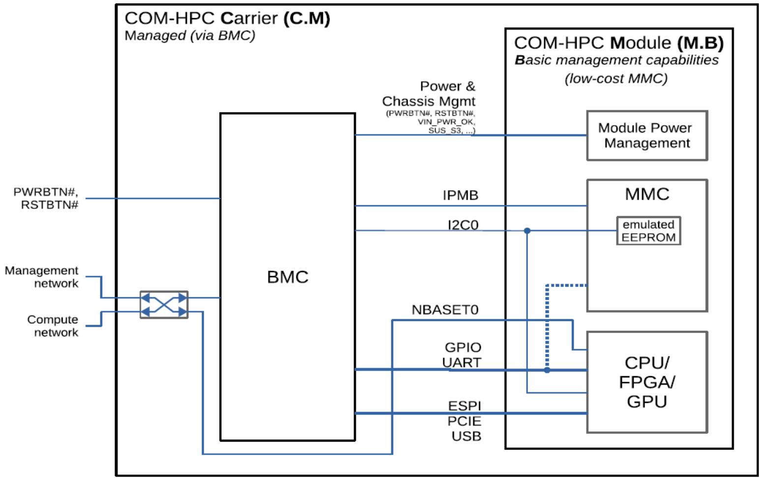
COM-HPC Module and Carrier boards may support out-of-band (OOB) management features. These features may be implemented on COM-HPC Server or Client systems. Traditionally OOB management is more of a server class feature, but the option is there for both COM-HPC Clients and Servers. There is a separate PICMG document that describes COM-HPC OOB management features in details — PICMG COM-HPC Platform Management Interface Specification. The management architecture is divided into BMC (Board Management Controller) and MMC (Module Management Controller), which are explained in the following sections.

BMC (Board Management Controller) (Located on Carrier board if deployed)

This is a microcontroller subsystem, usually based on the Carrier, that performs system out-of-band management functions such as firmware updates, power and reset control, performance monitoring and more. For COM-HPC module, which are hosted on the carrier, it may be a full subsystem with CPU / SOC, DRAM memory, an internal display controller and more. It may be ARM based. It may run a Linux or other OS. A popular vendor for this sort of BMC part is Aspeed, and in particular the Aspeed AST2510 and successor parts. Many other vendors and parts are possible.

It is anticipated that in most situations the BMC, if deployed, will be on the Carrier. Implementation of OOB management and a BMC on the Carrier is entirely optional. A Carrier based BMC is intended to work in conjunction with a Module based microcontroller referred to as the MMC (described below).

A Carrier BMC, if deployed, shall implement an IPMB interface to the COM-HPC Module. This is the channel for IPMI support. The Carrier BMC may also make use of the COM-HPC I2C0, USB, eSPI, NBASET0, UARTx and / or the PCIe\_BMC interfaces, as well as controlling the module power signals like PWRBTN, ...).

Any COM-HPC USB host port may be used to interface to a Carrier BMC USB client port. The Module USB port is usually a Module chipset or SOC host port, and not a MMC USB port. Designers should avoid using COM-HPC USB0, as it has special privileges allowing it to be used as a host or client. Designers may want to avoid using COM-HPC USB0, 1, 2, 3 as they are defined to allow USB SuperSpeed capability and BMC devices to not typically have USB SuperSpeed capability. USB4, 5, 6 or 7 should be used for the BMC interface if available.

Of the two COM-HPC UART interfaces that may be used to interface to a Carrier BMC, UART1 should be selected as UART0 is often used for functions such as Console Redirect.

# MMC (Module Management Controller) (Located on COM-HPC Module, optional)

The MMC is a Module based microcontroller that may work in conjunction with a Carrier based BMC. If there is no Carrier BMC, then the MMC shall fall back to a mode that does not depend on the Carrier BMC, allowing the Module to function without external OOB management. The MMC shall powered by the VCC\_5V\_SBY supply to allow for OOB functionality even when the main supply is not available, however, it should also use the main VCC rail, if available.

In most implementations, the MMC will be a relatively small low cost and low power device, in order to keep Module costs down for customers that do not require OOB management features. It may serve as a sensor aggregator. It may serve as host for nonvolatile Module parameter storage.

The MMC, if implemented, shall include an IPMB slave interface. It may additionally interface to the Carrier BMC over any of several other COM-HPC interfaces, including the I2C0 and or UART0 ports.

# Carrier and Module BMC and MMC Combinations

The PICMG COM-HPC Platform Management Interface Specification defines a number of different carrier and module options, which differ based on their management capabilities. Table 45 below lays out the options and defines a shorthand notation for the options. Full details are in the PICMG COM-HPC Platform Management Interface Specification.

Table 45: Carrier and Module BMC and MMC Combinations and Shorthand Notation

<table><tr><td></td><td>Shorthand Notation</td><td>Description</td></tr><tr><td rowspan="2">Carrier</td><td>C.U</td><td>UnmanagedThe carrier has no BMC. Power and chassis management is typically done via a small microcontrollerManagement depends on the Module&#x27;s capabilities</td></tr><tr><td>C.M</td><td>Managed via Carrier based BMCAn IPMB communication channel to the MMCShallbe implementedThe BMcamayalso make use of the NBASET0, eSPI, USB, I2C0, UART0, PCIe_BMC, and / or the GPIO interfacesProvides Redfish to the outside (or IPMI for legacy)iKVM for the module via PCIe_BMC/USB</td></tr><tr><td rowspan="3">Module</td><td>M.U</td><td>Unmanaged (No MMC)Shouldimplement a dedicated EEPROM (EeeP) for module identificationCPU management possible via I2C0, NBASET0, eSPI, USB, UART0, GPIO, PCIe_BMC (all except IPMB), depending on the Carrier capabilities</td></tr><tr><td>M.B</td><td>Basic Management capabilities via low cost MMCAn IPMB interface to Carrier BMCShallbe implementedManagement via external interfaces (IPMB, I2C0, NBASET0, eSPI, USB, UART0, GPIO, PCIe_BMC)</td></tr><tr><td>M.F</td><td>Full Management capabilities (typically via ARM-based OS)NBASET0 is shared by MMC and CPU (switched on Module), providing a high-speed OOB communication channelAn IPMB interface to Carrier BMCShallbe implementedAdditional interfacesmaybe used (I2C0, NBASET0, eSPI, USB, UART0, GPIO, PCIe_BMC)</td></tr></table>

Assuming that the Types of the Carrier and Module match up (Server with Server, Client with Client) and the board sizes / connector positions match up (size A, B, C or size D,E) then a C.U or C.M Carrier shall be basically operable with a M.U or M.B or M.F Module. The OOB management features may be missing, depending on what is matched with what. Additionally, there will likely be some vendor specific aspects to OOB management options.

M.B Module and C.M Carrier will be implemented at ADLINK COM-HPC Server Module and COM-HPC Server Carrier as first wave.
![**Labeled Blocks:**\n\n*   **COM-HPC Carrier (C.M)**\n    *   Managed (via BMC)\n*   **BMC**\n*   **PWRBTN#, RSTBTN#**\n*   **Management network**\n*   **Compute network**\n*   **COM-HPC Module (M.B)**\n    *   Basic management capabilities (low-cost MMC)\n*   **Power & Chassis Mgmt**\n    *   (PWRBTN#, RSTBTN#, VIN_PWR_OK, SUS_S3, ...)\n*   **Module Power Management**\n*   **IPMB**\n*   **I2C0**\n*   **MMC**\n    *   emulated EEPROM\n*   **NBASET0**\n*   **GPIO UART**\n*   **CPU/ FPGA/ GPU**\n*   **ESPI**\n*   **PCIE**\n*   **USB**\n\n**Connections:**\n\n*   A line connects the text 'PWRBTN#, RSTBTN#' to the 'BMC' block.\n*   Lines connect 'Management network' and 'Compute network' to a bidirectional switch symbol.\n*   A line connects the right output of the switch symbol to the 'BMC' block.\n*   A line connects the bottom output of the switch symbol to the line labeled 'NBASET0'.\n*   A line labeled 'Power & Chassis Mgmt (PWRBTN#, RSTBTN#, VIN_PWR_OK, SUS_S3, ...)' connects the 'BMC' block to the 'Module Power Management' block.\n*   A line labeled 'IPMB' connects the 'BMC' block to the 'MMC' block.\n*   A line labeled 'I2C0' connects the 'BMC' block to the 'emulated EEPROM' block inside the 'MMC' block. There is a junction dot on this line.\n*   A dotted line connects the junction dot on the 'I2C0' line to the 'CPU/ FPGA/ GPU' block.\n*   A line labeled 'NBASET0' connects the 'BMC' block to the 'CPU/ FPGA/ GPU' block.\n*   A line labeled 'GPIO UART' connects the 'BMC' block to the 'CPU/ FPGA/ GPU' block.\n*   Lines labeled 'ESPI', 'PCIE', and 'USB' connect the 'BMC' block to the 'CPU/ FPGA/ GPU' block.](.com-hpc-alt-50m-00115-1010-11/94d606e40e161cbf51d953342d6a87565c69c5e1a84281df6b38c2114e9bd4fc.jpg)

# IPMI on COM-HPC

The COM-HPC management platform shall use an IPMI (Intelligent Platform Management Interface) for communication between the Carrier BMC and MMC, over the COM-HPC IPMB port. The interface from the BMC to the user is independent from this, and may be realized using Redfish, it may support IPMI for legacy support. The interface used for IPMI between BMC and MMC shall be IPMB (an I2C bus specifically for IPMI use.

As set of IPMI commands for communication between MMC and BMC have been defined in the PICMG COM-HPC Platform Management Interface Specification. Most of those commands are not specific to COM-HPC, but defined in the IPMI specification and related specifications. However, also some COM-HPC specific commands have been developed. Specifically, the following command sets are covered:

- IPM Device Global Commands: Initialization and module discovery
- BMC Watchdog and Device and Messaging Commands: System interface and BMC interaction.
- Chassis Device Commands: Power control and boot options
- Event Commands: IPMI event handling
- PEF and Alerting Commands: Alerting and trigger support
- Sensor Device Commands: Sensor monitoring and housekeeping
- FRU Device Commands: Inventory data
- SDR Device Commands: Sensor information
- SEL Device Commands: System event logging
- LAN Device Commands and HPM.2: Support for Ethernet
- Serial/Modem Device Commands: For UART and SOL support
- AdvancedTCA subset: For Fan Management
- HPM.1: For Firmware update
- HPM.2: For managing BMC-MMC Ethernet communication
- COM-HPC specific Commands: For fast sensors and JTAG support

The inventory data available via IPMI FRU also includes information present in the COM-HPC EEPROM (see Section Error! Bookmark not defined.). The COM-HPC EEPROM content is defined in the PICMG Embedded EEPROM for COM-HPC document, a companion document to the PICMG COM-HPC Platform Management Interface Specification. The information available in the COM-HPC EEPROM area will be converted from EeeP format into IPMI FRU data structures by the MMC. In order to accomplish this, the MMC reads the data from the EEPROM during start of the system, and buffers the data internally to service incoming IPMI FRU accesses.

The EEPROM area for storing EeeP data may be implemented as a physical EEPROM on the board, on the I2C0 bus. Alternatively, it may be realized within the MMC. This is illustrated in Figure 10 above. In that figure, it is labeled as an “emulated EEPROM”. An I2C slave interface on the MMC is connected to the I2C0 bus of the COM-HPC module. This easesimplementation, as the MMC does not need to fetch information from the physical COM-HPC EEPROM, and also prevents potential access conflicts between the MMC and other I2C agents on the Baseboard or Carrier. The MMC implemented this way does not need I2C Master or Multi-Master capability.

# COM-HPC EEPROM

Modules and Carriers for COM-HPC should implement an EEPROM which allows the identification of Module or Carrier features via I2C. This feature is similar to the COM Express EEPROM defined in the PICMG COM Express specification. Some Module vendors will find a benefit in software reuse with test scripts and software infrastructure developed for COM Express use. The COM-HPC EEPROM content is defined in the EeeP for COM-HPC (Embedded EEPROM for COM-HPC) document, a companion document to the PICMG COM-HPC Platform Management Interface Specification. The EeeP for COM-HPC specification is derived from the Eeep for COM-Express document and introduces new data structures specific to COM-HPC modules and carriers, while the data structures for COM Express modules and carriers remain untouched. A new revision has been assigned to distinguish between COM Express and COM-HPC EEPROMs.

# EEPROM Device Information

If the COM Express Module and / or Carrier EEPROMs are implemented on COM-HPC, then the COM-HPC I2C0 port shall be used to interface to the EEPROMs. The EEPROM devices shall have a capacity of at least 32 Kbits, and shall have three address inputs. Suitable devices include the Atmel AT24C32C, the ST M24C32 and other compatible devices. Larger capacity devices may be used if they are compatible with the base 32 Kbit part referenced above.

# COM-HPC Module EEPROM

The Module should implement a serial EEPROM that identifies the Module using the EeeP defined Unique Device ID. In addition this EEPROM should describe the available module interfaces and capabilities as described in the EeeP for COM-HPC specification. The EEPROM may be implemented as a physical EEPROM on the board, or may be realized within the MMC (see Section Error! Bookmark not defined.).

The Module EEPROM allows the Carrier Board to set up any software configurable Carrier Board features in a way that is appropriate for the Module board. The Module EEPROM I2C device address lines, A2, A1 and A0 shall be pulled to a logic low, placing the device at address 0x50 (7 bit I2C addressing) and address 0xA0(8 bit I2C addressing). Note: I2C address A6-A3 are fixed at 1010b for I2C EEPROM devices per the I2C specification.

# COM-HPC Carrier Board EEPROM

The Carrier Board should implement a serial EEPROM that identifies the Carrier using the Unique Device Id and describes the expected PCI Express link configuration. In addition this EEPROM may describe the expected link presence for SATA, USB, DDI, VGA, LAN, audio, and the expected presence of miscellaneous I/O signals. The EEPROM may be implemented as a physical EEPROM on the board, or may be realized within the BMC (see Section

Error! Bookmark not defined.).

The Carrier EEPROM allows the Module firmware to set up any software configurable Module features in a way that is appropriate for the Carrier Board. If there is an incompatibility between the expected Carrier Board configuration and the Module capabilities, an error message may be generated. The error messaging is Module vendor specific and is not defined by this standard.

The Carrier EEPROM device address lines, A2, A1 and A0 shall be pulled to a logic high, placing the device at address 0x57 (7 bit addressing) and 0xAE(8 bit addressing). I2C addresses A6-A3 are fixed at 1010b for I2C EEPROM devices.

# 2.8 Debug

40 pin flat cable connector to be used with DB40 HPC debug module

Supports BIOS POST code LED, BMC access, SPI BIOS flashing, internal power rail test points, debug LEDs

# 2.9 Power

Power Modes: AT and ATX mode

Standard Voltage Input: ATX 12V±5% / 5Vsb ±5% or AT 12V±5%

Power Management: ACPI 5.0 compliant, Smart Battery support

Power States: C1-C6, S0, S1, S5, S5 ECO mode (Wake-on-USB, WoL S5)

ECO Mode support for deep S5 for 5Vsb power saving

# 2.10 Mechanical and Environmental

# Form Factor and Specification

PICMG COM-HPC Rev 1.0, Server Type, Size D 200 x 160 mm

Operating Temperature

<table><tr><td>Standard</td><td>0°C to 60°C at 12V</td><td>Storage: -20°C to 80°C</td></tr><tr><td>Industrial</td><td>-20°C to 70°C at 12V</td><td>Storage: -20°C to 80°C</td></tr></table>

Operate at -40°C to 85°C at 12V is by project basis discussion

# Humidity

5-90% RH operating, non-condensing, 5-95% RH storage (and operating with conformal coating)

# Shock and Vibration

IEC 60068-2-64 and IEC-60068-2-27

MIL-STD-202F, Method 213B, Table 213-I, Condition A and Method 214A, Table 214-I, Condition D

# HALT tested

Thermal Stress, Vibration Stress, Thermal Shock and Combined Test

# EMI

EN55032 Class B inside an enclosure

Ultrasound equipment will typically be sensitive to noise in the 1MHz to 20MHz band, we shall handle it well during these bands

# De-rating

De-rating file is provided by RD (delta temperature of some of components is based on the experience of previous products) and reviewed/approved by RRC team before each Gerber Out

Once we have real sample on-hand, the temperature of critical components shall be measured and feedback to the De-rating file to see if it still in specification.

# MTBF

200,000 hrs commercial 40℃ ambient (according MIL calculation) based on actual calculated de-rating

120,000 hrs ETT -20℃\~70℃ ambient (according MIL calculation) based on actual calculated de-rating (excludes the BCM57504 LAN controller)

# 3. Block Diagram

![**Left Column (J1)**\n*   **Header:** J1\n*   **Group Labels:** 'GROUP 0 Low', 'GROUP 0 High'\n*   **Labeled Blocks/Items:**\n    *   'PCIe Lane 0-3', 'PCIe Lane 4-7', 'PCIe Lane 8-11', 'PCIe Lane 12-15'\n    *   'PCIe_BMC x1'\n    *   'ETH_KR 0-3', 'ETH_KR 4-7'\n    *   '4x USB 3.x/2.0 0-3', '4x USB 2.0 4-7'\n    *   'SATA Port 0-1'\n    *   'NBASE-T 0'\n    *   'BOOT_SPI', 'GPP_SPI'\n    *   'SMBus'\n    *   'I2C 0 (w/ ALERT#)', 'I2C 1'\n    *   'UART 0', 'UART 1', 'GPIO x12'\n    *   'USB_PD_IPMB', 'eSPI'\n\n**Central Block**\n*   **Main Labels:** 'Ampere Computing', 'Altra'\n*   **Top Labels:** '(Root Complex B)', 'can be x8', '(Root Complex B)', 'can be x8', '(Root Complex A)', '(Root Complex A)'\n*   **Side Labels:** 'PCIe x8', 'PCIe x1', 'I2C_9', 'HSUART', 'HSUART', 'HSUART'\n\n**Right Column (J2)**\n*   **Header:** J2\n*   **Group Labels:** 'GROUP 1', 'GROUP 2', 'GROUP 3'\n*   **Labeled Blocks/Items:**\n    *   'PCIe Lane 16-31', 'PCIe Lane 32-47', 'PCIe Lane 48-63'\n    *   'ETH_Sidebands', 'Rapid_Shutdown'\n\n**Intermediary and Peripheral Blocks**\n*   **Small Blue Boxes:** 'BCM57502', 'µPD720201', 'LAN Intel i210', 'BIOS', 'TPM', 'EEPROM', 'MMC ATMEGA'\n*   **Bottom Blocks:** 'Discrete (power sequence)', Six blocks labeled 'DIMM 3200 MT/s'\n*   **Other Text:** 'Sensor for monitoring voltage/current/temp', 'UART_1 RTS#, CTS# simulated by GPIO'\n\n**Connections and Line Labels**\n*   **Top Left:** Lines labeled '1 x4, 2 x2' connect 'PCIe Lane 0-3' and 'PCIe Lane 4-7' to the center block. Lines labeled '2 x2, 1 x4' connect 'PCIe Lane 8-11' and 'PCIe Lane 12-15' to the center block.\n*   **Right Side:** Lines labeled '1 x16, 2 x8, 4 x4' connect 'PCIe Lane 16-31', 'PCIe Lane 32-47', and 'PCIe Lane 48-63' to the center block.\n*   **Specific Connections:**\n    *   'ETH_KR 0-3' connects to 'BCM57502', which connects to 'PCIe x8' on the center block.\n    *   '4x USB 3.x/2.0 0-3' connects to 'µPD720201', which connects to 'PCIe x1' on the center block.\n    *   'NBASE-T 0' connects to 'LAN Intel i210', which connects to the center block.\n    *   'BOOT_SPI' connects to 'BIOS', which connects to the center block.\n    *   'GPP_SPI' connects to 'TPM', which connects to the center block.\n    *   'SMBus' connects to 'EEPROM', which connects to 'I2C_9' on the center block.\n    *   'USB_PD_IPMB', 'eSPI', and 'Sensor for monitoring voltage/current/temp' all connect to 'MMC ATMEGA'.](.com-hpc-alt-50m-00115-1010-11/3bae57313298a6c9a4ee2afb4befc2cdaaf9a07dbd0b4c1698d46cf0f045f455.jpg)

Note:
-All the PCIe are Gen4
-I2C\_9 from Altra SOC supports CCIX mode code (ready now) or general purpose SMBUS mode code (TBC), either one
-UART\_1: TX, RX come from SOC, RTS#, CTS# are simulated by SOC GPIO
-USB\_PD\_I2C, MMC, SOC: connect together
-need work with AST2500 Remote BMC on carrier

Figure 1 – Functional block diagram

# 4. Pinout and Signal Descriptions

# 4.1 Pin Summary

The below table is a comprehensive list of all signal pins supported on the dual 400-pin COM-HPC connectors (J1 and J2) as defined for Server Type in the PICMG COM-HPC Rev 1.0 specification. Signals described in the specification but not supported on the COM-HPC-ALT are marked by strikethrough ROW A/B/C/D on J1 connector, ROW E/F/G/H on J2 connector

![J2\nPIN H100\nPIN E01\nSize E\n(200 x 160mm)\nJ1\nPIN A01\nPIN D100](.com-hpc-alt-50m-00115-1010-11/bd86c64fcadeafb0dd5822edcd6f40c08fd28f2e564aadc161a6bb7c3cce74c1.jpg)

Figure 2 – Rear side row

<table><tr><td colspan="2">Row A</td><td></td><td colspan="2">Row B</td><td></td><td colspan="2">Row C</td><td></td><td colspan="2">Row D</td></tr><tr><td>A1</td><td>VCC</td><td></td><td>B1</td><td>VCC</td><td></td><td>C1</td><td>VCC</td><td></td><td>D1</td><td>VCC</td></tr><tr><td>A2</td><td>VCC</td><td></td><td>B2</td><td>PWRBTN#</td><td></td><td>C2</td><td>RSTBTN#</td><td></td><td>D2</td><td>VCC</td></tr><tr><td>A3</td><td>VCC</td><td></td><td>B3</td><td>VCC</td><td></td><td>C3</td><td>VCC</td><td></td><td>D3</td><td>VCC</td></tr><tr><td>A4</td><td>VCC</td><td></td><td>B4</td><td>THERMTRIP#</td><td></td><td>C4</td><td>CARRIER_HOT#</td><td></td><td>D4</td><td>VCC</td></tr><tr><td>A5</td><td>VCC</td><td></td><td>B5</td><td>VCC</td><td></td><td>C5</td><td>VCC</td><td></td><td>D5</td><td>VCC</td></tr><tr><td>A6</td><td>VCC</td><td></td><td>B6</td><td>TAMPER#</td><td></td><td>C6</td><td>VIN_PWR_OK</td><td></td><td>D6</td><td>VCC</td></tr><tr><td>A7</td><td>VCC</td><td></td><td>B7</td><td>VCC</td><td></td><td>C7</td><td>VCC</td><td></td><td>D7</td><td>VCC</td></tr><tr><td>A8</td><td>VCC</td><td></td><td>B8</td><td>SUS_S3#</td><td></td><td>C8</td><td>SUS_S4_S5#</td><td></td><td>D8</td><td>VCC</td></tr><tr><td>A9</td><td>VCC</td><td></td><td>B9</td><td>VCC</td><td></td><td>C9</td><td>VCC</td><td></td><td>D9</td><td>VCC</td></tr><tr><td>A10</td><td>GND</td><td></td><td>B10</td><td>WD_STROBE#</td><td></td><td>C10</td><td>GND</td><td></td><td>D10</td><td>WAKE0#</td></tr><tr><td>A11</td><td>BATLOW#</td><td></td><td>B11</td><td>WD_OUT</td><td></td><td>C11</td><td>FAN_PWMOUT</td><td></td><td>D11</td><td>WAKE1#</td></tr><tr><td>A12</td><td>PLTRST#</td><td></td><td>B12</td><td>GND</td><td></td><td>C12</td><td>FAN_TACHIN</td><td></td><td>D12</td><td>GND</td></tr><tr><td>A13</td><td>GND</td><td></td><td>B13</td><td>USB5-</td><td></td><td>C13</td><td>GND</td><td></td><td>D13</td><td>USB1-</td></tr><tr><td>A14</td><td>USB7-</td><td></td><td>B14</td><td>USB5+</td><td></td><td>C14</td><td>USB3-</td><td></td><td>D14</td><td>USB1+</td></tr><tr><td>A15</td><td>USB7+</td><td></td><td>B15</td><td>GND</td><td></td><td>C15</td><td>USB3+</td><td></td><td>D15</td><td>GND</td></tr><tr><td>A16</td><td>GND</td><td></td><td>B16</td><td>USB4-</td><td></td><td>C16</td><td>GND</td><td></td><td>D16</td><td>USB0-</td></tr><tr><td>A17</td><td>USB6-</td><td></td><td>B17</td><td>USB4+</td><td></td><td>C17</td><td>USB2-</td><td></td><td>D17</td><td>USB0+</td></tr><tr><td>A18</td><td>USB6+</td><td></td><td>B18</td><td>GND</td><td></td><td>C18</td><td>USB2+</td><td></td><td>D18</td><td>GND</td></tr><tr><td>A19</td><td>GND</td><td></td><td>B19</td><td>RSVD</td><td></td><td>C19</td><td>GND</td><td></td><td>D19</td><td>ETH0_RX-</td></tr><tr><td>A20</td><td>ETH4_RX-</td><td></td><td>B20</td><td>RSVD</td><td></td><td>C20</td><td>ETH0_TX-</td><td></td><td>D20</td><td>ETH0_RX+</td></tr><tr><td>A21</td><td>ETH4_RX+</td><td></td><td>B21</td><td>RSVD</td><td></td><td>C21</td><td>ETH0_TX+</td><td></td><td>D21</td><td>GND</td></tr><tr><td>A22</td><td>GND</td><td></td><td>B22</td><td>RSVD</td><td></td><td>C22</td><td>GND</td><td></td><td>D22</td><td>ETH1_RX-</td></tr><tr><td>A23</td><td>ETH5_RX-</td><td></td><td>B23</td><td>RSVD</td><td></td><td>C23</td><td>ETH1_TX-</td><td></td><td>D23</td><td>ETH1_RX+</td></tr><tr><td>A24</td><td>ETH5_RX+</td><td></td><td>B24</td><td>VCC_5V_SBY</td><td></td><td>C24</td><td>ETH1_TX+</td><td></td><td>D24</td><td>GND</td></tr><tr><td>A25</td><td>GND</td><td></td><td>B25</td><td>USB67_OC#</td><td></td><td>C25</td><td>GND</td><td></td><td>D25</td><td>ETH2_RX-</td></tr><tr><td>A26</td><td>ETH6_RX-</td><td></td><td>B26</td><td>USB45_OC#</td><td></td><td>C26</td><td>ETH2_TX-</td><td></td><td>D26</td><td>ETH2_RX+</td></tr><tr><td>A27</td><td>ETH6_RX+</td><td></td><td>B27</td><td>USB23_OC#</td><td></td><td>C27</td><td>ETH2_TX+</td><td></td><td>D27</td><td>GND</td></tr><tr><td>A28</td><td>GND</td><td></td><td>B28</td><td>USB01_OC#</td><td></td><td>C28</td><td>GND</td><td></td><td>D28</td><td>ETH3_RX-</td></tr><tr><td>A29</td><td>ETH7_RX-</td><td></td><td>B29</td><td>SML1_CLK</td><td></td><td>C29</td><td>ETH3_TX-</td><td></td><td>D29</td><td>ETH3_RX+</td></tr><tr><td>A30</td><td>ETH7_RX+</td><td></td><td>B30</td><td>SML1_DAT</td><td></td><td>C30</td><td>ETH3_TX+</td><td></td><td>D30</td><td>GND</td></tr><tr><td>A31</td><td>GND</td><td></td><td>B31</td><td>PMCALERT#</td><td></td><td>C31</td><td>GND</td><td></td><td>D31</td><td>USB3_SSTX-</td></tr><tr><td>A32</td><td>RSVD</td><td></td><td>B32</td><td>SML0_CLK</td><td></td><td>C32</td><td>USB3_SSRX-</td><td></td><td>D32</td><td>USB3_SSTX+</td></tr><tr><td>A33</td><td>RSVD</td><td></td><td>B33</td><td>SML0_DAT</td><td></td><td>C33</td><td>USB3_SSRX+</td><td></td><td>D33</td><td>GND</td></tr><tr><td>A34</td><td>GND</td><td></td><td>B34</td><td>USB_PD_ALERT#</td><td></td><td>C34</td><td>GND</td><td></td><td>D34</td><td>USB2_SSTX-</td></tr><tr><td>A35</td><td>ETH4_TX-</td><td></td><td>B35</td><td>USB_PD_I2C_CLK</td><td></td><td>C35</td><td>USB2_SSRX-</td><td></td><td>D35</td><td>USB2_SSTX+</td></tr><tr><td>A36</td><td>ETH4_TX+</td><td></td><td>B36</td><td>USB_PD_I2C_DAT</td><td></td><td>C36</td><td>USB2_SSRX+</td><td></td><td>D36</td><td>GND</td></tr><tr><td>A37</td><td>GND</td><td></td><td>B37</td><td>USB_RT_ENA</td><td></td><td>C37</td><td>GND</td><td></td><td>D37</td><td>USB1_SSTX0-</td></tr><tr><td>A38</td><td>ETH5_TX-</td><td></td><td>B38</td><td>USB1_LSRX</td><td></td><td>C38</td><td>USB1_SSRX0-</td><td></td><td>D38</td><td>USB1_SSTX0+</td></tr><tr><td>A39</td><td>ETH5_TX+</td><td></td><td>B39</td><td>USB1_LSTX</td><td></td><td>C39</td><td>USB1_SSRX0+</td><td></td><td>D39</td><td>GND</td></tr><tr><td>A40</td><td>GND</td><td></td><td>B40</td><td>USB0_LSRX</td><td></td><td>C40</td><td>GND</td><td></td><td>D40</td><td>USB1_SSTX1-</td></tr><tr><td>A41</td><td>ETH6_TX-</td><td></td><td>B41</td><td>USB0_LSTX</td><td></td><td>C41</td><td>USB1_SSRX1-</td><td></td><td>D41</td><td>USB1_SSTX1+</td></tr><tr><td>A42</td><td>ETH6_TX+</td><td></td><td>B42</td><td>GND</td><td></td><td>C42</td><td>USB1_SSRX1+</td><td></td><td>D42</td><td>GND</td></tr><tr><td>A43</td><td>GND</td><td></td><td>B43</td><td>USB0_AUX-</td><td></td><td>C43</td><td>GND</td><td></td><td>D43</td><td>USB0_SSTX0-</td></tr><tr><td>A44</td><td>ETH7_TX-</td><td></td><td>B44</td><td>USB0_AUX+</td><td></td><td>C44</td><td>USB0_SSRX0-</td><td></td><td>D44</td><td>USB0_SSTX0+</td></tr><tr><td>A45</td><td>ETH7_TX+</td><td></td><td>B45</td><td>RSVD</td><td></td><td>C45</td><td>USB0_SSRX0+</td><td></td><td>D45</td><td>GND</td></tr><tr><td>A46</td><td>GND</td><td></td><td>B46</td><td>RSVD</td><td></td><td>C46</td><td>GND</td><td></td><td>D46</td><td>USB0_SSTX1-</td></tr><tr><td>A47</td><td>USB1_AUX-</td><td></td><td>B47</td><td>VCC_BOOT_SPI</td><td></td><td>C47</td><td>USB0_SSRX1-</td><td></td><td>D47</td><td>USB0_SSTX1+</td></tr><tr><td>A48</td><td>USB1_AUX+</td><td></td><td>B48</td><td>BOOT_SPI_CS#</td><td></td><td>C48</td><td>USB0_SSRX1+</td><td></td><td>D48</td><td>GND</td></tr><tr><td>A49</td><td>GND</td><td></td><td>B49</td><td>BSEL0</td><td></td><td>C49</td><td>GND</td><td></td><td>D49</td><td>SATA0_RX-</td></tr><tr><td>A50</td><td>eSPI_IO0</td><td></td><td>B50</td><td>BSEL1</td><td></td><td>C50</td><td>BOOT_SPI_IO0</td><td></td><td>D50</td><td>SATA0_RX+</td></tr><tr><td>A51</td><td>eSPI_IO1</td><td></td><td>B51</td><td>BSEL2</td><td></td><td>C51</td><td>BOOT_SPI_IO1</td><td></td><td>D51</td><td>GND</td></tr><tr><td>A52</td><td>eSPI_IO2</td><td></td><td>B52</td><td>eSPI_ALERT0#</td><td></td><td>C52</td><td>BOOT_SPI_IO2</td><td></td><td>D52</td><td>SATA0_TX-</td></tr><tr><td>A53</td><td>eSPI_IO3</td><td></td><td>B53</td><td>eSPI_ALERT1#</td><td></td><td>C53</td><td>BOOT_SPI_IO3</td><td></td><td>D53</td><td>SATA0_TX+</td></tr><tr><td>A54</td><td>eSPI_CLK</td><td></td><td>B54</td><td>eSPI_CS0#</td><td></td><td>C54</td><td>BOOT_SPI_CLK</td><td></td><td>D54</td><td>GND</td></tr><tr><td>A55</td><td>GND</td><td></td><td>B55</td><td>eSPI_CS1#</td><td></td><td>C55</td><td>GND</td><td></td><td>D55</td><td>SATA1_RX-</td></tr><tr><td>A56</td><td>PCIe_CLKREQ0_LO#</td><td></td><td>B56</td><td>eSPI_RST#</td><td></td><td>C56</td><td>PCIe_REFCLK0_HI-</td><td></td><td>D56</td><td>SATA1_RX+</td></tr><tr><td>A57</td><td>PCIe_CLKREQ0_HI#</td><td></td><td>B57</td><td>GND</td><td></td><td>C57</td><td>PCIe_REFCLK0_HI+</td><td></td><td>D57</td><td>GND</td></tr><tr><td>A58</td><td>GND</td><td></td><td>B58</td><td>PCIe_BMC_RX-</td><td></td><td>C58</td><td>GND</td><td></td><td>D58</td><td>SATA1_TX-</td></tr><tr><td>A59</td><td>PCIe_BMC_TX-</td><td></td><td>B59</td><td>PCIe_BMC_RX+</td><td></td><td>C59</td><td>PCIe_REFCLK0_LO-</td><td></td><td>D59</td><td>SATA1_TX+</td></tr><tr><td>A60</td><td>PCIe_BMC_TX+</td><td></td><td>B60</td><td>GND</td><td></td><td>C60</td><td>PCIe_REFCLK0_LO+</td><td></td><td>D60</td><td>GND</td></tr><tr><td>A61</td><td>GND</td><td></td><td>B61</td><td>PCIe08_RX-</td><td></td><td>C61</td><td>GND</td><td></td><td>D61</td><td>PCIe00_TX-</td></tr><tr><td>A62</td><td>PCIe08_TX-</td><td></td><td>B62</td><td>PCIe08_RX+</td><td></td><td>C62</td><td>PCIe00_RX-</td><td></td><td>D62</td><td>PCIe00_TX+</td></tr><tr><td>A63</td><td>PCIe08_TX+</td><td></td><td>B63</td><td>GND</td><td></td><td>C63</td><td>PCIe00_RX+</td><td></td><td>D63</td><td>GND</td></tr><tr><td>A64</td><td>GND</td><td></td><td>B64</td><td>PCIe09_RX-</td><td></td><td>C64</td><td>GND</td><td></td><td>D64</td><td>PCIe01_TX-</td></tr><tr><td>A65</td><td>PCIe09_TX-</td><td></td><td>B65</td><td>PCIe09_RX+</td><td></td><td>C65</td><td>PCIe01_RX-</td><td></td><td>D65</td><td>PCIe01_TX+</td></tr><tr><td>A66</td><td>PCIe09_TX+</td><td></td><td>B66</td><td>GND</td><td></td><td>C66</td><td>PCIe01_RX+</td><td></td><td>D66</td><td>GND</td></tr><tr><td>A67</td><td>GND</td><td></td><td>B67</td><td>PCIe10_RX-</td><td></td><td>C67</td><td>GND</td><td></td><td>D67</td><td>PCIe02_TX-</td></tr><tr><td>A68</td><td>PCIe10_TX-</td><td></td><td>B68</td><td>PCIe10_RX+</td><td></td><td>C68</td><td>PCIe02_RX-</td><td></td><td>D68</td><td>PCIe02_TX+</td></tr><tr><td>A69</td><td>PCIe10_TX+</td><td></td><td>B69</td><td>GND</td><td></td><td>C69</td><td>PCIe02_RX+</td><td></td><td>D69</td><td>GND</td></tr><tr><td>A70</td><td>GND</td><td></td><td>B70</td><td>PCIe11_RX-</td><td></td><td>C70</td><td>GND</td><td></td><td>D70</td><td>PCIe03_TX-</td></tr><tr><td>A71</td><td>PCIe11_TX-</td><td></td><td>B71</td><td>PCIe11_RX+</td><td></td><td>C71</td><td>PCIe03_RX-</td><td></td><td>D71</td><td>PCIe03_TX+</td></tr><tr><td>A72</td><td>PCIe11_TX+</td><td></td><td>B72</td><td>GND</td><td></td><td>C72</td><td>PCIe03_RX+</td><td></td><td>D72</td><td>GND</td></tr><tr><td>A73</td><td>GND</td><td></td><td>B73</td><td>PCIe12_RX-</td><td></td><td>C73</td><td>GND</td><td></td><td>D73</td><td>PCIe04_TX-</td></tr><tr><td>A74</td><td>PCIe12_TX-</td><td></td><td>B74</td><td>PCIe12_RX+</td><td></td><td>C74</td><td>PCIe04_RX-</td><td></td><td>D74</td><td>PCIe04_TX+</td></tr><tr><td>A75</td><td>PCIe12_TX+</td><td></td><td>B75</td><td>GND</td><td></td><td>C75</td><td>PCIe04_RX+</td><td></td><td>D75</td><td>GND</td></tr><tr><td>A76</td><td>GND</td><td></td><td>B76</td><td>PCIe13_RX-</td><td></td><td>C76</td><td>GND</td><td></td><td>D76</td><td>PCIe05_TX-</td></tr><tr><td>A77</td><td>PCIe13_TX-</td><td></td><td>B77</td><td>PCIe13_RX+</td><td></td><td>C77</td><td>PCIe05_RX-</td><td></td><td>D77</td><td>PCIe05_TX+</td></tr><tr><td>A78</td><td>PCIe13_TX+</td><td></td><td>B78</td><td>GND</td><td></td><td>C78</td><td>PCIe05_RX+</td><td></td><td>D78</td><td>GND</td></tr><tr><td>A79</td><td>GND</td><td></td><td>B79</td><td>PCIe14_RX-</td><td></td><td>C79</td><td>GND</td><td></td><td>D79</td><td>PCIe06_TX-</td></tr><tr><td>A80</td><td>PCIe14_TX-</td><td></td><td>B80</td><td>PCIe14_RX+</td><td></td><td>C80</td><td>PCIe06_RX-</td><td></td><td>D80</td><td>PCIe06_TX+</td></tr><tr><td>A81</td><td>PCIe14_TX+</td><td></td><td>B81</td><td>GND</td><td></td><td>C81</td><td>PCIe06_RX+</td><td></td><td>D81</td><td>GND</td></tr><tr><td>A82</td><td>GND</td><td></td><td>B82</td><td>PCIe15_RX-</td><td></td><td>C82</td><td>GND</td><td></td><td>D82</td><td>PCIe07_TX-</td></tr><tr><td>A83</td><td>PCIe15_TX-</td><td></td><td>B83</td><td>PCIe15_RX+</td><td></td><td>C83</td><td>PCIe07_RX-</td><td></td><td>D83</td><td>PCIe07_TX+</td></tr><tr><td>A84</td><td>PCIe15_TX+</td><td></td><td>B84</td><td>GND</td><td></td><td>C84</td><td>PCIe07_RX+</td><td></td><td>D84</td><td>GND</td></tr><tr><td>A85</td><td>GND</td><td></td><td>B85</td><td>RSVD</td><td></td><td>C85</td><td>GND</td><td></td><td>D85</td><td>NBASET0_MDIO-</td></tr><tr><td>A86</td><td>VCC_RTC</td><td></td><td>B86</td><td>RSMRST_OUT#</td><td></td><td>C86</td><td>SMB_CLK</td><td></td><td>D86</td><td>NBASET0_MDIO+</td></tr><tr><td>A87</td><td>SUS_CLK</td><td></td><td>B87</td><td>UART1_TX</td><td></td><td>C87</td><td>SMB_DAT</td><td></td><td>D87</td><td>GND</td></tr><tr><td>A88</td><td>GPIO_00</td><td></td><td>B88</td><td>UART1_RX</td><td></td><td>C88</td><td>SMB_ALERT#</td><td></td><td>D88</td><td>NBASET0_MDI1-</td></tr><tr><td>A89</td><td>GPIO_01</td><td></td><td>B89</td><td>UART1_RTS#</td><td></td><td>C89</td><td>UART0_TX</td><td></td><td>D89</td><td>NBASET0_MDI1+</td></tr><tr><td>A90</td><td>GPIO_02</td><td></td><td>B90</td><td>UART1_CTS#</td><td></td><td>C90</td><td>UART0_RX</td><td></td><td>D90</td><td>GND</td></tr><tr><td>A91</td><td>GPIO_03</td><td></td><td>B91</td><td>IPMB_CLK</td><td></td><td>C91</td><td>UART0_RTS#</td><td></td><td>D91</td><td>NBASET0_MDI2-</td></tr><tr><td>A92</td><td>GPIO_04</td><td></td><td>B92</td><td>IPMB_DAT</td><td></td><td>C92</td><td>UART0_CTS#</td><td></td><td>D92</td><td>NBASET0_MDI2+</td></tr><tr><td>A93</td><td>GPIO_05</td><td></td><td>B93</td><td>GPSPI_MOSI</td><td></td><td>C93</td><td>I2C0_CLK</td><td></td><td>D93</td><td>GND</td></tr><tr><td>A94</td><td>GPIO_06</td><td></td><td>B94</td><td>GPSPI_MISO</td><td></td><td>C94</td><td>I2C0_DAT</td><td></td><td>D94</td><td>NBASET0_MDI3-</td></tr><tr><td>A95</td><td>GPIO_07</td><td></td><td>B95</td><td>GPSPI_CS0#</td><td></td><td>C95</td><td>I2C0_ALERT#</td><td></td><td>D95</td><td>NBASET0_MDI3+</td></tr><tr><td>A96</td><td>GPIO_08</td><td></td><td>B96</td><td>GPSPI_CS1#</td><td></td><td>C96</td><td>I2C1_CLK</td><td></td><td>D96</td><td>GND</td></tr><tr><td>A97</td><td>GPIO_09</td><td></td><td>B97</td><td>GPSPI_CS2#</td><td></td><td>C97</td><td>I2C1_DAT</td><td></td><td>D97</td><td>NBASET0_LINK_MAX#</td></tr><tr><td>A98</td><td>GPIO_10</td><td></td><td>B98</td><td>GPSPI_CS3#</td><td></td><td>C98</td><td>NBASET0_SDP</td><td></td><td>D98</td><td>NBASET0_LINK_MID#</td></tr><tr><td>A99</td><td>GPIO_11</td><td></td><td>B99</td><td>GPSPI_CLK</td><td></td><td>C99</td><td>NBASET0_CTREF</td><td></td><td>D99</td><td>NBASET0_LINK_ACT#</td></tr><tr><td>A100</td><td>TYPE0</td><td></td><td>B100</td><td>GPSPI_ALERT#</td><td></td><td>C100</td><td>TYPE1</td><td></td><td>D100</td><td>TYPE2</td></tr><tr><td colspan="2">Row E</td><td></td><td colspan="2">Row F</td><td></td><td colspan="2">Row G</td><td></td><td colspan="2">Row H</td></tr><tr><td>E1</td><td>RAPID_SHUTDOWN</td><td></td><td>F1</td><td>ETH2_SDP</td><td></td><td>G1</td><td>RSVD</td><td></td><td>H1</td><td>RSVD</td></tr><tr><td>E2</td><td>GND</td><td></td><td>F2</td><td>ETH3_SDP</td><td></td><td>G2</td><td>RSVD</td><td></td><td>H2</td><td>RSVD</td></tr><tr><td>E3</td><td>RSVD</td><td></td><td>F3</td><td>ETH4_SDP</td><td></td><td>G3</td><td>RSVD</td><td></td><td>H3</td><td>RSVD</td></tr><tr><td>E4</td><td>RSVD</td><td></td><td>F4</td><td>ETH5_SDP</td><td></td><td>G4</td><td>RSVD</td><td></td><td>H4</td><td>RSVD</td></tr><tr><td>E5</td><td>GND</td><td></td><td>F5</td><td>ETH6_SDP</td><td></td><td>G5</td><td>RSVD</td><td></td><td>H5</td><td>RSVD</td></tr><tr><td>E6</td><td>RSVD</td><td></td><td>F6</td><td>ETH7_SDP</td><td></td><td>G6</td><td>RSVD</td><td></td><td>H6</td><td>RSVD</td></tr><tr><td>E7</td><td>RSVD</td><td></td><td>F7</td><td>ETH4-7_I2C_CLK</td><td></td><td>G7</td><td>RSVD</td><td></td><td>H7</td><td>RSVD</td></tr><tr><td>E8</td><td>GND</td><td></td><td>F8</td><td>ETH4-7_I2C_DAT</td><td></td><td>G8</td><td>RSVD</td><td></td><td>H8</td><td>RSVD</td></tr><tr><td>E9</td><td>RSVD</td><td></td><td>F9</td><td>ETH4-7_INT#</td><td></td><td>G9</td><td>RSVD</td><td></td><td>H9</td><td>RSVD</td></tr><tr><td>E10</td><td>RSVD</td><td></td><td>F10</td><td>ETH4-7_MDIO_CLK</td><td></td><td>G10</td><td>RSVD</td><td></td><td>H10</td><td>RSVD</td></tr><tr><td>E11</td><td>GND</td><td></td><td>F11</td><td>ETH4-7_MDIO_DAT</td><td></td><td>G11</td><td>RSVD</td><td></td><td>H11</td><td>RSVD</td></tr><tr><td>E12</td><td>RSVD</td><td></td><td>F12</td><td>ETH4-7_PHY_INT#</td><td></td><td>G12</td><td>RSVD</td><td></td><td>H12</td><td>RSVD</td></tr><tr><td>E13</td><td>RSVD</td><td></td><td>F13</td><td>ETH4-7_PHY_RST#</td><td></td><td>G13</td><td>RSVD</td><td></td><td>H13</td><td>RSVD</td></tr><tr><td>E14</td><td>GND</td><td></td><td>F14</td><td>ETH4-7_PRSNT#</td><td></td><td>G14</td><td>GND</td><td></td><td>H14</td><td>RSVD</td></tr><tr><td>E15</td><td>RSVD</td><td></td><td>F15</td><td>RSVD</td><td></td><td>G15</td><td>RSVD</td><td></td><td>H15</td><td>RSVD</td></tr><tr><td>E16</td><td>RSVD</td><td></td><td>F16</td><td>RSVD</td><td></td><td>G16</td><td>RSVD</td><td></td><td>H16</td><td>RSVD</td></tr><tr><td>E17</td><td>GND</td><td></td><td>F17</td><td>RSVD</td><td></td><td>G17</td><td>RSVD</td><td></td><td>H17</td><td>RSVD</td></tr><tr><td>E18</td><td>RSVD</td><td></td><td>F18</td><td>RSVD</td><td></td><td>G18</td><td>RSVD</td><td></td><td>H18</td><td>RSVD</td></tr><tr><td>E19</td><td>RSVD</td><td></td><td>F19</td><td>GND</td><td></td><td>G19</td><td>RSVD</td><td></td><td>H19</td><td>GND</td></tr><tr><td>E20</td><td>GND</td><td></td><td>F20</td><td>PCIe32_RX-</td><td></td><td>G20</td><td>GND</td><td></td><td>H20</td><td>PCIe40_TX-</td></tr><tr><td>E21</td><td>PCIe32_TX-</td><td></td><td>F21</td><td>PCIe32_RX+</td><td></td><td>G21</td><td>PCIe40_RX-</td><td></td><td>H21</td><td>PCIe40_TX+</td></tr><tr><td>E22</td><td>PCIe32_TX+</td><td></td><td>F22</td><td>GND</td><td></td><td>G22</td><td>PCIe40_RX+</td><td></td><td>H22</td><td>GND</td></tr><tr><td>E23</td><td>GND</td><td></td><td>F23</td><td>PCIe33_RX-</td><td></td><td>G23</td><td>GND</td><td></td><td>H23</td><td>PCIe41_TX-</td></tr><tr><td>E24</td><td>PCIe33_TX-</td><td></td><td>F24</td><td>PCIe33_RX+</td><td></td><td>G24</td><td>PCIe41_RX-</td><td></td><td>H24</td><td>PCIe41_TX+</td></tr><tr><td>E25</td><td>PCIe33_TX+</td><td></td><td>F25</td><td>GND</td><td></td><td>G25</td><td>PCIe41_RX+</td><td></td><td>H25</td><td>GND</td></tr><tr><td>E26</td><td>GND</td><td></td><td>F26</td><td>PCIe34_RX-</td><td></td><td>G26</td><td>GND</td><td></td><td>H26</td><td>PCIe42_TX-</td></tr><tr><td>E27</td><td>PCIe34_TX-</td><td></td><td>F27</td><td>PCIe34_RX+</td><td></td><td>G27</td><td>PCIe42_RX-</td><td></td><td>H27</td><td>PCIe42_TX+</td></tr><tr><td>E28</td><td>PCIe34_TX+</td><td></td><td>F28</td><td>GND</td><td></td><td>G28</td><td>PCIe42_RX+</td><td></td><td>H28</td><td>GND</td></tr><tr><td>E29</td><td>GND</td><td></td><td>F29</td><td>PCIe35_RX-</td><td></td><td>G29</td><td>GND</td><td></td><td>H29</td><td>PCIe43_TX-</td></tr><tr><td>E30</td><td>PCIe35_TX-</td><td></td><td>F30</td><td>PCIe35_RX+</td><td></td><td>G30</td><td>PCIe43_RX-</td><td></td><td>H30</td><td>PCIe43_TX+</td></tr><tr><td>E31</td><td>PCIe35_TX+</td><td></td><td>F31</td><td>GND</td><td></td><td>G31</td><td>PCIe43_RX+</td><td></td><td>H31</td><td>GND</td></tr><tr><td>E32</td><td>GND</td><td></td><td>F32</td><td>PCIe36_RX-</td><td></td><td>G32</td><td>GND</td><td></td><td>H32</td><td>PCIe44_TX-</td></tr><tr><td>E33</td><td>PCIe36_TX-</td><td></td><td>F33</td><td>PCIe36_RX+</td><td></td><td>G33</td><td>PCIe44_RX-</td><td></td><td>H33</td><td>PCIe44_TX+</td></tr><tr><td>E34</td><td>PCIe36_TX+</td><td></td><td>F34</td><td>GND</td><td></td><td>G34</td><td>PCIe44_RX+</td><td></td><td>H34</td><td>GND</td></tr><tr><td>E35</td><td>GND</td><td></td><td>F35</td><td>PCIe37_RX-</td><td></td><td>G35</td><td>GND</td><td></td><td>H35</td><td>PCIe45_TX-</td></tr><tr><td>E36</td><td>PCIe37_TX-</td><td></td><td>F36</td><td>PCIe37_RX+</td><td></td><td>G36</td><td>PCIe45_RX-</td><td></td><td>H36</td><td>PCIe45_TX+</td></tr><tr><td>E37</td><td>PCIe37_TX+</td><td></td><td>F37</td><td>GND</td><td></td><td>G37</td><td>PCIe45_RX+</td><td></td><td>H37</td><td>GND</td></tr><tr><td>E38</td><td>GND</td><td></td><td>F38</td><td>PCIe38_RX-</td><td></td><td>G38</td><td>GND</td><td></td><td>H38</td><td>PCIe46_TX-</td></tr><tr><td>E39</td><td>PCIe38_TX-</td><td></td><td>F39</td><td>PCIe38_RX+</td><td></td><td>G39</td><td>PCIe46_RX-</td><td></td><td>H39</td><td>PCIe46_TX+</td></tr><tr><td>E40</td><td>PCIe38_TX+</td><td></td><td>F40</td><td>GND</td><td></td><td>G40</td><td>PCIe46_RX+</td><td></td><td>H40</td><td>GND</td></tr><tr><td>E41</td><td>GND</td><td></td><td>F41</td><td>PCIe39_RX-</td><td></td><td>G41</td><td>GND</td><td></td><td>H41</td><td>PCIe47_TX-</td></tr><tr><td>E42</td><td>PCIe39_TX-</td><td></td><td>F42</td><td>PCIe39_RX+</td><td></td><td>G42</td><td>PCIe47_RX-</td><td></td><td>H42</td><td>PCIe47_TX+</td></tr><tr><td>E43</td><td>PCIe39_TX+</td><td></td><td>F43</td><td>GND</td><td></td><td>G43</td><td>PCIe47_RX+</td><td></td><td>H43</td><td>GND</td></tr><tr><td>E44</td><td>GND</td><td></td><td>F44</td><td>PCIe16_RX-</td><td></td><td>G44</td><td>GND</td><td></td><td>H44</td><td>PCIe24_TX-</td></tr><tr><td>E45</td><td>PCIe16_TX-</td><td></td><td>F45</td><td>PCIe16_RX+</td><td></td><td>G45</td><td>PCIe24_RX-</td><td></td><td>H45</td><td>PCIe24_TX+</td></tr><tr><td>E46</td><td>PCIe16_TX+</td><td></td><td>F46</td><td>GND</td><td></td><td>G46</td><td>PCIe24_RX+</td><td></td><td>H46</td><td>GND</td></tr><tr><td>E47</td><td>GND</td><td></td><td>F47</td><td>PCIe17_RX-</td><td></td><td>G47</td><td>GND</td><td></td><td>H47</td><td>PCIe25_TX-</td></tr><tr><td>E48</td><td>PCIe17_TX-</td><td></td><td>F48</td><td>PCIe17_RX+</td><td></td><td>G48</td><td>PCIe25_RX-</td><td></td><td>H48</td><td>PCIe25_TX+</td></tr><tr><td>E49</td><td>PCIe17_TX+</td><td></td><td>F49</td><td>GND</td><td></td><td>G49</td><td>PCIe25_RX+</td><td></td><td>H49</td><td>GND</td></tr><tr><td>E50</td><td>GND</td><td></td><td>F50</td><td>PCIe18_RX-</td><td></td><td>G50</td><td>GND</td><td></td><td>H50</td><td>PCIe26_TX-</td></tr><tr><td>E51</td><td>PCIe18_TX-</td><td></td><td>F51</td><td>PCIe18_RX+</td><td></td><td>G51</td><td>PCIe26_RX-</td><td></td><td>H51</td><td>PCIe26_TX+</td></tr><tr><td>E52</td><td>PCIe18_TX+</td><td></td><td>F52</td><td>GND</td><td></td><td>G52</td><td>PCIe26_RX+</td><td></td><td>H52</td><td>GND</td></tr><tr><td>E53</td><td>GND</td><td></td><td>F53</td><td>PCIe19_RX-</td><td></td><td>G53</td><td>GND</td><td></td><td>H53</td><td>PCIe27_TX-</td></tr><tr><td>E54</td><td>PCIe19_TX-</td><td></td><td>F54</td><td>PCIe19_RX+</td><td></td><td>G54</td><td>PCIe27_RX-</td><td></td><td>H54</td><td>PCIe27_TX+</td></tr><tr><td>E55</td><td>PCIe19_TX+</td><td></td><td>F55</td><td>GND</td><td></td><td>G55</td><td>PCIe27_RX+</td><td></td><td>H55</td><td>GND</td></tr><tr><td>E56</td><td>GND</td><td></td><td>F56</td><td>PCIe20_RX-</td><td></td><td>G56</td><td>GND</td><td></td><td>H56</td><td>PCIe28_TX-</td></tr><tr><td>E57</td><td>PCIe20_TX-</td><td></td><td>F57</td><td>PCIe20_RX+</td><td></td><td>G57</td><td>PCIe28_RX-</td><td></td><td>H57</td><td>PCIe28_TX+</td></tr><tr><td>E58</td><td>PCIe20_TX+</td><td></td><td>F58</td><td>GND</td><td></td><td>G58</td><td>PCIe28_RX+</td><td></td><td>H58</td><td>GND</td></tr><tr><td>E59</td><td>GND</td><td></td><td>F59</td><td>PCIe21_RX-</td><td></td><td>G59</td><td>GND</td><td></td><td>H59</td><td>PCIe29_TX-</td></tr><tr><td>E60</td><td>PCIe21_TX-</td><td></td><td>F60</td><td>PCIe21_RX+</td><td></td><td>G60</td><td>PCIe29_RX-</td><td></td><td>H60</td><td>PCIe29_TX+</td></tr><tr><td>E61</td><td>PCIe21_TX+</td><td></td><td>F61</td><td>GND</td><td></td><td>G61</td><td>PCIe29_RX+</td><td></td><td>H61</td><td>GND</td></tr><tr><td>E62</td><td>GND</td><td></td><td>F62</td><td>PCIe22_RX-</td><td></td><td>G62</td><td>GND</td><td></td><td>H62</td><td>PCIe30_TX-</td></tr><tr><td>E63</td><td>PCIe22_TX-</td><td></td><td>F63</td><td>PCIe22_RX+</td><td></td><td>G63</td><td>PCIe30_RX-</td><td></td><td>H63</td><td>PCIe30_TX+</td></tr><tr><td>E64</td><td>PCIe22_TX+</td><td></td><td>F64</td><td>GND</td><td></td><td>G64</td><td>PCIe30_RX+</td><td></td><td>H64</td><td>GND</td></tr><tr><td>E65</td><td>GND</td><td></td><td>F65</td><td>PCIe23_RX-</td><td></td><td>G65</td><td>GND</td><td></td><td>H65</td><td>PCIe31_TX-</td></tr><tr><td>E66</td><td>PCIe23_TX-</td><td></td><td>F66</td><td>PCIe23_RX+</td><td></td><td>G66</td><td>PCIe31_RX-</td><td></td><td>H66</td><td>PCIe31_TX+</td></tr><tr><td>E67</td><td>PCIe23_TX+</td><td></td><td>F67</td><td>GND</td><td></td><td>G67</td><td>PCIe31_RX+</td><td></td><td>H67</td><td>GND</td></tr><tr><td>E68</td><td>GND</td><td></td><td>F68</td><td>PCIe48_RX-</td><td></td><td>G68</td><td>GND</td><td></td><td>H68</td><td>PCIe56_TX-</td></tr><tr><td>E69</td><td>PCIe48_TX-</td><td></td><td>F69</td><td>PCIe48_RX+</td><td></td><td>G69</td><td>PCIe56_RX-</td><td></td><td>H69</td><td>PCIe56_TX+</td></tr><tr><td>E70</td><td>PCIe48_TX+</td><td></td><td>F70</td><td>GND</td><td></td><td>G70</td><td>PCIe56_RX+</td><td></td><td>H70</td><td>GND</td></tr><tr><td>E71</td><td>GND</td><td></td><td>F71</td><td>PCIe49_RX-</td><td></td><td>G71</td><td>GND</td><td></td><td>H71</td><td>PCIe57_TX-</td></tr><tr><td>E72</td><td>PCIe49_TX-</td><td></td><td>F72</td><td>PCIe49_RX+</td><td></td><td>G72</td><td>PCIe57_RX-</td><td></td><td>H72</td><td>PCIe57_TX+</td></tr><tr><td>E73</td><td>PCIe49_TX+</td><td></td><td>F73</td><td>GND</td><td></td><td>G73</td><td>PCIe57_RX+</td><td></td><td>H73</td><td>GND</td></tr><tr><td>E74</td><td>GND</td><td></td><td>F74</td><td>PCIe50_RX-</td><td></td><td>G74</td><td>GND</td><td></td><td>H74</td><td>PCIe58_TX-</td></tr><tr><td>E75</td><td>PCIe50_TX-</td><td></td><td>F75</td><td>PCIe50_RX+</td><td></td><td>G75</td><td>PCIe58_RX-</td><td></td><td>H75</td><td>PCIe58_TX+</td></tr><tr><td>E76</td><td>PCIe50_TX+</td><td></td><td>F76</td><td>GND</td><td></td><td>G76</td><td>PCIe58_RX+</td><td></td><td>H76</td><td>GND</td></tr><tr><td>E77</td><td>GND</td><td></td><td>F77</td><td>PCIe51_RX-</td><td></td><td>G77</td><td>GND</td><td></td><td>H77</td><td>PCIe59_TX-</td></tr><tr><td>E78</td><td>PCIe51_TX-</td><td></td><td>F78</td><td>PCIe51_RX+</td><td></td><td>G78</td><td>PCIe59_RX-</td><td></td><td>H78</td><td>PCIe59_TX+</td></tr><tr><td>E79</td><td>PCIe51_TX+</td><td></td><td>F79</td><td>GND</td><td></td><td>G79</td><td>PCIe59_RX+</td><td></td><td>H79</td><td>GND</td></tr><tr><td>E80</td><td>GND</td><td></td><td>F80</td><td>PCIe52_RX-</td><td></td><td>G80</td><td>GND</td><td></td><td>H80</td><td>PCIe60_TX-</td></tr><tr><td>E81</td><td>PCIe52_TX-</td><td></td><td>F81</td><td>PCIe52_RX+</td><td></td><td>G81</td><td>PCIe60_RX-</td><td></td><td>H81</td><td>PCIe60_TX+</td></tr><tr><td>E82</td><td>PCIe52_TX+</td><td></td><td>F82</td><td>GND</td><td></td><td>G82</td><td>PCIe60_RX+</td><td></td><td>H82</td><td>GND</td></tr><tr><td>E83</td><td>GND</td><td></td><td>F83</td><td>PCIe53_RX-</td><td></td><td>G83</td><td>GND</td><td></td><td>H83</td><td>PCIe61_TX-</td></tr><tr><td>E84</td><td>PCIe53_TX-</td><td></td><td>F84</td><td>PCIe53_RX+</td><td></td><td>G84</td><td>PCIe61_RX-</td><td></td><td>H84</td><td>PCIe61_TX+</td></tr><tr><td>E85</td><td>PCIe53_TX+</td><td></td><td>F85</td><td>GND</td><td></td><td>G85</td><td>PCIe61_RX+</td><td></td><td>H85</td><td>GND</td></tr><tr><td>E86</td><td>GND</td><td></td><td>F86</td><td>PCIe54_RX-</td><td></td><td>G86</td><td>GND</td><td></td><td>H86</td><td>PCIe62_TX-</td></tr><tr><td>E87</td><td>PCIe54_TX-</td><td></td><td>F87</td><td>PCIe54_RX+</td><td></td><td>G87</td><td>PCIe62_RX-</td><td></td><td>H87</td><td>PCIe62_TX+</td></tr><tr><td>E88</td><td>PCIe54_TX+</td><td></td><td>F88</td><td>GND</td><td></td><td>G88</td><td>PCIe62_RX+</td><td></td><td>H88</td><td>GND</td></tr><tr><td>E89</td><td>GND</td><td></td><td>F89</td><td>PCIe55_RX-</td><td></td><td>G89</td><td>GND</td><td></td><td>H89</td><td>PCIe63_TX-</td></tr><tr><td>E90</td><td>PCIe55_TX-</td><td></td><td>F90</td><td>PCIe55_RX+</td><td></td><td>G90</td><td>PCIe63_RX-</td><td></td><td>H90</td><td>PCIe63_TX+</td></tr><tr><td>E91</td><td>PCIe55_TX+</td><td></td><td>F91</td><td>GND</td><td></td><td>G91</td><td>PCIe63_RX+</td><td></td><td>H91</td><td>GND</td></tr><tr><td>E92</td><td>GND</td><td></td><td>F92</td><td>PCIe_REFCLK2-</td><td></td><td>G92</td><td>GND</td><td></td><td>H92</td><td>PCIe_REFCLKIN0-</td></tr><tr><td>E93</td><td>PCIe_REFCLK1-</td><td></td><td>F93</td><td>PCIe_REFCLK2+</td><td></td><td>G93</td><td>PCIe_REFCLK3-</td><td></td><td>H93</td><td>PCIe_REFCLKIN0+</td></tr><tr><td>E94</td><td>PCIe_REFCLK1+</td><td></td><td>F94</td><td>GND</td><td></td><td>G94</td><td>PCIe_REFCLK3+</td><td></td><td>H94</td><td>GND</td></tr><tr><td>E95</td><td>GND</td><td></td><td>F95</td><td>PCIe_CLKREQ3#</td><td></td><td>G95</td><td>GND</td><td></td><td>H95</td><td>PCIe_REFCLKIN1-</td></tr><tr><td>E96</td><td>PCIe_CLKREQ1#</td><td></td><td>F96</td><td>ETH0-3_PRSNT#</td><td></td><td>G96</td><td>ETH0-3_I2C_CLK</td><td></td><td>H96</td><td>PCIe_REFCLKIN1+</td></tr><tr><td>E97</td><td>PCIe_CLKREQ2#</td><td></td><td>F97</td><td>ETH0-3_PHY_RST#</td><td></td><td>G97</td><td>ETH0-3_I2C_DAT</td><td></td><td>H97</td><td>GND</td></tr><tr><td>E98</td><td>PCIe_CLKREQ_OUT0#</td><td></td><td>F98</td><td>ETH0_SDP</td><td></td><td>G98</td><td>ETH0-3_PHY_INT#</td><td></td><td>H98</td><td>ETH0-3_MDIO_CLK</td></tr><tr><td>E99</td><td>PCIe_CLKREQ_OUT1#</td><td></td><td>F99</td><td>ETH1_SDP</td><td></td><td>G99</td><td>ETH0-3_INT#</td><td></td><td>H99</td><td>ETH0-3_MDIO_DAT</td></tr><tr><td>E100</td><td>PCIe_PERST_IN0#</td><td></td><td>F100</td><td>PCIe_PERST_IN1#</td><td></td><td>G100</td><td>PCIe_WAKE_OUT0#</td><td></td><td>H100</td><td>PCIe_WAKE_OUT1#</td></tr></table>

![The image features a red icon on a white background. It depicts a document or memo shape with the top-right corner folded down. Inside the red outline, there are two horizontal lines centered horizontally, representing text.](.com-hpc-alt-50m-00115-1010-11/8c0e34f5c540f9b04600b27c90e90a2a2e8d6d26fc13adf4a56671f6bfae0219.jpg)
Note: Strikethrough entries are functions not supported by this product.
IPMB is supported if there’s MMC on module. No eSPI support on this platform

# 4.2 Signal Terminology Descriptions

Definitions of the terms used for signal description tables

<table><tr><td>Term</td><td>Description</td></tr><tr><td colspan="2"></td></tr><tr><td>I</td><td>Input to the module</td></tr><tr><td>O</td><td>Output from the module</td></tr><tr><td>I/O</td><td>Bi-directional Input / Output</td></tr><tr><td>OD</td><td>Open drain output from the module</td></tr><tr><td></td><td></td></tr><tr><td>I 3.3V</td><td>Input 3.3V tolerant</td></tr><tr><td>I 5V</td><td>Input 5V tolerant</td></tr><tr><td>O 3.3V</td><td>Output 3.3V signal level</td></tr><tr><td>O 5V</td><td>Output 5V signal level</td></tr><tr><td>I/O 3.3V</td><td>Bi-directional signal 3.3V tolerant</td></tr><tr><td>I/O 5V</td><td>Bi-directional signal 5V tolerant</td></tr><tr><td>I/O  $3.3V_{SB}$ </td><td>Input or output 3.3V tolerant active in standby state</td></tr><tr><td></td><td></td></tr><tr><td>DDC</td><td>Display Data Channel</td></tr><tr><td>PCIE</td><td>PCI Express compatible differential signal</td></tr><tr><td>PEG</td><td>PCI Express Graphics</td></tr><tr><td>SATA</td><td>Serial ATA specification Revision 2.6 and 3</td></tr><tr><td>LVDS</td><td>Low Voltage Differential Signal - 330 mV nominal; 450 mV maximum differential signal</td></tr><tr><td></td><td></td></tr><tr><td>P</td><td>Power Input / Output</td></tr><tr><td>REF</td><td>Reference voltage output. May be sourced from a Module power plane.</td></tr><tr><td>PDS</td><td>Pull-down strap. A Module output pin that is either tied to GND or is not connected.Used to signal Module capabilities to the Carrier Board.</td></tr><tr><td></td><td></td></tr><tr><td>PU</td><td>PU (pull-up) resistor on module</td></tr><tr><td>PD</td><td>PD (pull-down) resistor on module</td></tr></table>

# 4.3 Signal Descriptions on J1/J2 Connectors

# 4.3.1 Ethernet KR/KX

Ethernet KR interface are defined for COM-HPC. For these ports, the Ethernet MACs are located on COM-HPC module. PHYs (if used) are on the Carrier. In some cases, no PHY is required, for short cable (“Direct Attach” cables) or Carrier runs.

COM-HPC support both of MDIO and I2C control interfaces for the PHYs. The MDIO and I2C control interfaces are grouped into quads, for KR ports 0:3 and ports 4:7

<table><tr><td>Name</td><td>Pin #</td><td>Description</td><td>I/O</td><td>PU / PD</td><td>Comment</td></tr><tr><td>ETH0_TX-</td><td>C20</td><td>Ethernet KR ports, transmit output differential pairs.</td><td>O</td><td></td><td>AC coupled Off Module</td></tr><tr><td>ETH0_TX+</td><td>C21</td><td></td><td>KR</td><td></td><td></td></tr><tr><td>ETH1_TX-</td><td>C23</td><td></td><td></td><td></td><td></td></tr><tr><td>ETH1_TX+</td><td>C24</td><td></td><td></td><td></td><td></td></tr><tr><td>ETH2_TX-</td><td>C26</td><td></td><td></td><td></td><td></td></tr><tr><td>ETH2_TX+</td><td>C27</td><td></td><td></td><td></td><td></td></tr><tr><td>ETH3_TX-</td><td>C29</td><td></td><td></td><td></td><td></td></tr><tr><td>ETH3_TX+</td><td>C30</td><td></td><td></td><td></td><td></td></tr><tr><td>ETH0_RX-</td><td>D19</td><td>Ethernet KR ports, receive input differential pairs.</td><td>I</td><td></td><td>AC coupled Off Module</td></tr><tr><td>ETH0_RX+</td><td>D20</td><td></td><td>KR</td><td></td><td></td></tr><tr><td>ETH1_RX-</td><td>D22</td><td></td><td></td><td></td><td></td></tr><tr><td>ETH1_RX+</td><td>D23</td><td></td><td></td><td></td><td></td></tr><tr><td>ETH2_RX-</td><td>D25</td><td></td><td></td><td></td><td></td></tr><tr><td>ETH2_RX+</td><td>D26</td><td></td><td></td><td></td><td></td></tr><tr><td>ETH3_RX-</td><td>D28</td><td></td><td></td><td></td><td></td></tr><tr><td>ETH3_RX+</td><td>D29</td><td></td><td></td><td></td><td></td></tr><tr><td>ETH0-3_MDIO_DAT</td><td>H99</td><td>Management Data I/O interface mode data signal for serial data transfers between the MAC and an external PHY for ETHx ports 0 to 3</td><td>I/O3.3VSB</td><td>PU 2K2</td><td>Not Supported</td></tr><tr><td>ETH0-3_MDIO_CLK</td><td>H98</td><td>Clock signal for Management Data I/O interface mode data signal for serial data transfers between the MAC and an external PHY for ETHx ports 0 to 3</td><td>O3.3VSB</td><td></td><td>Not Supported</td></tr><tr><td>ETH0-3_INT#</td><td>G99</td><td>Active low interrupt signal from IO Port expanders for ETH ports 0 to 3</td><td>I3.3VSB</td><td>PU 4K7</td><td></td></tr><tr><td>ETH0-3_PHY_INT#</td><td>G98</td><td>Active low PHY interrupt signal from ETH ports 0 to 3</td><td>I3.3VSB</td><td>PU 4K7</td><td></td></tr><tr><td>ETH0-3_PHY_RST#</td><td>F97</td><td>Active low output PHY reset signal for ETH ports 0 to 3.</td><td>O3.3VSB</td><td></td><td></td></tr><tr><td>ETH0-3_I2C_DAT</td><td>G97</td><td>I2C data signal of the 2-wire management interface used by the Ethernet KR controller to access the management registers of an external SFP Module or to configure the Carrier PHY for ETHx ports 0 to 3 and for serialized status information (e.g. LED states)..</td><td>I/O OD3.3VSB</td><td>PU 1K</td><td></td></tr><tr><td>ETH0-3_I2C_CLK</td><td>G96</td><td>The I2C clock signals associated with ETH0-3 I2C data lines in the row above.</td><td>I/O OD3.3VSB</td><td>PU 1K</td><td></td></tr><tr><td>ETH0_SDP</td><td>F98</td><td rowspan="4">Software-Definable Pins. Can also be used for IEEE1588 support such as a PPS signal.</td><td rowspan="4">I/O3.3VSB</td><td rowspan="4"></td><td rowspan="4">Not Supported</td></tr><tr><td>ETH1_SDP</td><td>F99</td></tr><tr><td>ETH2_SDP</td><td>F1</td></tr><tr><td>ETH3_SDP</td><td>F2</td></tr><tr><td>ETH0-3_PRSNT#</td><td>F96</td><td>Carrier pulls this line to GND if there is Carrier hardware present to support Ethernet KR signalling on ETH0 through ETH3. If the entire KR quad is not supported it should fill from ETH0 on up.</td><td>I3.3VSB</td><td>PU 4K7</td><td></td></tr></table>

![The image shows a reddish-pink outline icon representing a document or page. It is roughly square-shaped with a folded bottom-right corner (a 'dog-ear'). Inside the outline, there are two horizontal lines centered vertically, resembling text or a list.](.com-hpc-alt-50m-00115-1010-11/ec3539a5ea159321f99d9498c6b4bd1e6ff8c2009e10fac3333f25608c912128.jpg)
Note: The Ethernet KR support is 10GBASE-KR

# 4.3.2 NBASE-T Ethernet

The port may operate in 10Gbps, 5Gbps, 2.5Gbps, 1Gbps, 100Mbps, or 10Mbps modes. Magnetics are to be on the Carrier board. The COM-HPC module shall be capable of 1000BASE-T mode.

<table><tr><td>Name</td><td>Pin #</td><td colspan="4">Description</td><td>I/O</td><td>PU / PD</td><td>Comment</td></tr><tr><td rowspan="6">NBASET0_MD10-NBASET0_MD10+NBASET0_MD11-NBASET0_MD11+NBASET0_MD12-NBASET0_MD12+NBASET0_MD13-NBASET0_MD13+</td><td rowspan="6">D85D86D88D89D91D92D93D94</td><td colspan="4">Ethernet Controller 1: Media Dependent Interface Differential Pairs0,1,2,3. The MDI can operate in 10Gbps, 1Gbps, 100Mbps and 10Mbps modes. Some pairs are unused in some modes, per the following:</td><td rowspan="6">I/O Analog</td><td rowspan="6"></td><td rowspan="6">Twisted pair signals for external transformer.</td></tr><tr><td> $\phi$ </td><td>10000BASE-T $\phi$ 1000BASE-T $\phi$ </td><td>100BASE-TX $\phi$ </td><td>10BASE-T $\phi$ </td></tr><tr><td>MDI[0]+/~ $\phi$ </td><td>B1_DA+/- $\phi$ </td><td>TX+/- $\phi$ </td><td>TX+/- $\phi$ </td></tr><tr><td>MDI[1]+/~ $\phi$ </td><td>B1_DB+/- $\phi$ </td><td>RX+/- $\phi$ </td><td>RX+/- $\phi$ </td></tr><tr><td>MDI[2]+/~ $\phi$ </td><td>B1_DC+/- $\phi$ </td><td> $\phi$ </td><td> $\phi$ </td></tr><tr><td>MDI[3]+/~ $\phi$ </td><td>B1_DD+/-  $\phi$ </td><td> $\phi$ </td><td> $\phi$ </td></tr><tr><td>NBASET0_LINK_ACT#</td><td>D99</td><td colspan="4">NBASE-T Ethernet Controller activity indicator, active low.20 mA or more current sink capability at VOL of 0.4V max.20 mA or more current source capability at VOH of 2.4V min.</td><td>O 3.3VSB</td><td></td><td>Need add pull-high on carrier board</td></tr><tr><td>NBASET0_LINK_MAX#</td><td>D97</td><td colspan="4">NBASE-T Ethernet Controller MAX Speed Link indicator, active low. If active, the link is established at the maximum speed that the Ethernet controller is capable of (which may be 10G, 5G, 2.5G etc).20 mA or more current sink capability at VOL of 0.4V max.20 mA or more current source capability at VOH of 2.4V min.</td><td>O 3.3VSB</td><td></td><td></td></tr><tr><td>NBASET0_LINK_MID#</td><td>D98</td><td colspan="4">NBASE-T Ethernet Controller MID Speed Link indicator, active low. If active, the link is established but at a speed lower than what the maximum speed that the Ethernet controller is capable of.20 mA or more current sink capability at VOL of 0.4V max.20 mA or more current source capability at VOH of 2.4V min.</td><td>O 3.3VSB</td><td></td><td></td></tr><tr><td>NBASET0_CTREF</td><td>C99</td><td colspan="4">Reference voltage for Carrier Board NBASET Ethernet channel 0 magnetics center tap. The reference voltage is determined by the requirements of the Module PHY and may be as low as 0V and as high as 3.3V. If not needed, these pins may be left open on the Carrier. The reference voltage output shall be current limited on the Module. In the case in which the reference is shorted to ground, the current shall be limited to 250 mA or less.</td><td>REFGND min3.3V max</td><td></td><td>Not Supported</td></tr><tr><td>NBASET0_SDP</td><td>C98</td><td colspan="4">NBASE-T Ethernet Controller 0 Software-Definable Pin. Can also be used for IEEE1588 support such as a 1pps signal.</td><td>IO 3.3VSB</td><td></td><td></td></tr></table>

4.3.3 PCI Express

<table><tr><td>Name</td><td>Pin #</td><td>Description</td><td>I/O</td><td>PU / PD</td><td>Comment</td></tr><tr><td colspan="6"></td></tr><tr><td>PCIe00_TX+</td><td>D62</td><td>PCI Express Differential Transmit Pairs 0-7</td><td rowspan="16">O PCIe</td><td rowspan="16"></td><td rowspan="16">AC coupled on Module</td></tr><tr><td>PCIe00_TX-</td><td>D61</td><td rowspan="15">PCIe Group 0 Low</td></tr><tr><td>PCIe01_TX+</td><td>D65</td></tr><tr><td>PCIe01_TX-</td><td>D64</td></tr><tr><td>PCIe02_TX+</td><td>D68</td></tr><tr><td>PCIe03_TX-</td><td>D67</td></tr><tr><td>PCIe03_TX+</td><td>D71</td></tr><tr><td>PCIe03_TX-</td><td>D70</td></tr><tr><td>PCIe04_TX+</td><td>D74</td></tr><tr><td>PCIe04_TX-</td><td>D73</td></tr><tr><td>PCIe05_TX+</td><td>D77</td></tr><tr><td>PCIe05_TX-</td><td>D76</td></tr><tr><td>PCIe06_TX+</td><td>D80</td></tr><tr><td>PCIe06_TX-</td><td>D79</td></tr><tr><td>PCIe07_TX+</td><td>D83</td></tr><tr><td>PCIe07_TX-</td><td>D82</td></tr><tr><td>PCIe00_RX+</td><td>C63</td><td>PCI Express Differential Receive Pairs 0-7</td><td rowspan="16">I PCIe</td><td rowspan="16"></td><td rowspan="16">AC coupled off Module</td></tr><tr><td>PCIe00_RX-</td><td>C62</td><td rowspan="15">PCIe Group 0 Low</td></tr><tr><td>PCIe01_RX+</td><td>C66</td></tr><tr><td>PCIe01_RX-</td><td>C65</td></tr><tr><td>PCIe02_RX+</td><td>C69</td></tr><tr><td>PCIe02_RX-</td><td>C68</td></tr><tr><td>PCIe03_RX+</td><td>C72</td></tr><tr><td>PCIe03_RX-</td><td>C71</td></tr><tr><td>PCIe04_RX+</td><td>C75</td></tr><tr><td>PCIe04_RX-</td><td>C74</td></tr><tr><td>PCIe05_RX+</td><td>C78</td></tr><tr><td>PCIe05_RX-</td><td>C77</td></tr><tr><td>PCIe06_RX+</td><td>C81</td></tr><tr><td>PCIe06_RX-</td><td>C80</td></tr><tr><td>PCIe07_RX+</td><td>C84</td></tr><tr><td>PCIe07_RX-</td><td>C83</td></tr><tr><td>PCIe08_TX+</td><td>A63</td><td>PCI Express Differential Transmit Pairs 8-15</td><td rowspan="2">O PCIe</td><td rowspan="2"></td><td rowspan="2">AC coupled on Module</td></tr><tr><td>PCIe08_TX-PCIe09_TX+</td><td>A62A66</td><td>PCIe Group 0 HighA Server Module may map up to 8 higher bandwidth PCIe lanes to Group 0 High</td></tr><tr><td>PCIe09_TX-</td><td>A65</td><td rowspan="13"></td><td rowspan="13"></td><td rowspan="13"></td><td rowspan="13"></td></tr><tr><td>PCIe10_TX+</td><td>A69</td></tr><tr><td>PCIe10_TX-</td><td>A68</td></tr><tr><td>PCIe11_TX+</td><td>A72</td></tr><tr><td>PCIe11_TX-</td><td>A71</td></tr><tr><td>PCIe12_TX+</td><td>A75</td></tr><tr><td>PCIe12_TX-</td><td>A74</td></tr><tr><td>PCIe13_TX+</td><td>A78</td></tr><tr><td>PCIe13_TX-</td><td>A77</td></tr><tr><td>PCIe14_TX+</td><td>A81</td></tr><tr><td>PCIe14_TX-</td><td>A80</td></tr><tr><td>PCIe15_TX+</td><td>A84</td></tr><tr><td>PCIe15_TX-</td><td>A83</td></tr><tr><td>PCIe08_RX+</td><td>B62</td><td>PCI Express Differential Receive Pairs 8-15</td><td rowspan="16">I PCIe</td><td rowspan="16"></td><td rowspan="16">AC coupled off Module</td></tr><tr><td>PCIe08_RX-</td><td>B61</td><td>PCIe Group 0 High</td></tr><tr><td>PCIe09_RX+</td><td>B65</td><td>A Server Module may map up to 8 higher bandwidth</td></tr><tr><td>PCIe09_RX-</td><td>B64</td><td rowspan="13">PCIe lanes to Group 0 High</td></tr><tr><td>PCIe10_RX+</td><td>B68</td></tr><tr><td>PCIe10_RX-</td><td>B67</td></tr><tr><td>PCIe11_RX+</td><td>B71</td></tr><tr><td>PCIe11_RX-</td><td>B70</td></tr><tr><td>PCIe12_RX+</td><td>B74</td></tr><tr><td>PCIe12_RX-</td><td>B73</td></tr><tr><td>PCIe13_RX+</td><td>B77</td></tr><tr><td>PCIe13_RX-</td><td>B76</td></tr><tr><td>PCIe14_RX+</td><td>B80</td></tr><tr><td>PCIe14_RX-</td><td>B79</td></tr><tr><td>PCIe15_RX+</td><td>B83</td></tr><tr><td>PCIe15_RX-</td><td>B82</td></tr><tr><td>PCIe16_TX+</td><td>E46</td><td>PCI Express Differential Transmit Pairs 16-31</td><td rowspan="9">O PCIe</td><td rowspan="9"></td><td rowspan="9">AC coupled on Module</td></tr><tr><td>PCIe16_TX-</td><td>E46</td><td rowspan="8">PCIe Group 1</td></tr><tr><td>PCIe17_TX+</td><td>E49</td></tr><tr><td>PCIe17_TX-</td><td>E48</td></tr><tr><td>PCIe18_TX+</td><td>E52</td></tr><tr><td>PCIe18_TX-</td><td>E51</td></tr><tr><td>PCIe19_TX+</td><td>E55</td></tr><tr><td>PCIe19_TX-</td><td>E54</td></tr><tr><td>PCIe20_TX+</td><td>E58</td></tr><tr><td>PCIe20_TX-</td><td>E57</td><td></td><td></td><td></td><td></td></tr><tr><td>PCIe21_TX+</td><td>E61</td><td></td><td></td><td></td><td></td></tr><tr><td>PCIe21_TX-</td><td>E60</td><td></td><td></td><td></td><td></td></tr><tr><td>PCIe22_TX+</td><td>E64</td><td></td><td></td><td></td><td></td></tr><tr><td>PCIe22_TX-</td><td>E63</td><td></td><td></td><td></td><td></td></tr><tr><td>PCIe23_TX+</td><td>E67</td><td></td><td></td><td></td><td></td></tr><tr><td>PCIe23_TX-</td><td>E66</td><td></td><td></td><td></td><td></td></tr><tr><td>PCIe24_TX+</td><td>H45</td><td></td><td></td><td></td><td></td></tr><tr><td>PCIe24_TX-</td><td>H44</td><td></td><td></td><td></td><td></td></tr><tr><td>PCIe25_TX+</td><td>H48</td><td></td><td></td><td></td><td></td></tr><tr><td>PCIe25_TX-</td><td>H47</td><td></td><td></td><td></td><td></td></tr><tr><td>PCIe26_TX+</td><td>H51</td><td></td><td></td><td></td><td></td></tr><tr><td>PCIe26_TX-</td><td>H50</td><td></td><td></td><td></td><td></td></tr><tr><td>PCIe27_TX+</td><td>H54</td><td></td><td></td><td></td><td></td></tr><tr><td>PCIe27_TX-</td><td>H53</td><td></td><td></td><td></td><td></td></tr><tr><td>PCIe28_TX+</td><td>H57</td><td></td><td></td><td></td><td></td></tr><tr><td>PCIe28_TX-</td><td>H56</td><td></td><td></td><td></td><td></td></tr><tr><td>PCIe29_TX+</td><td>H60</td><td></td><td></td><td></td><td></td></tr><tr><td>PCIe29_TX-</td><td>H59</td><td></td><td></td><td></td><td></td></tr><tr><td>PCIe30_TX+</td><td>H63</td><td></td><td></td><td></td><td></td></tr><tr><td>PCIe30_TX-</td><td>H62</td><td></td><td></td><td></td><td></td></tr><tr><td>PCIe31_TX+</td><td>H66</td><td></td><td></td><td></td><td></td></tr><tr><td>PCIe31_TX-</td><td>H65</td><td></td><td></td><td></td><td></td></tr><tr><td>PCIe16_RX+</td><td>F45</td><td rowspan="16">PCI Express Differential Receive Pairs 16-31PCIe Group 1</td><td rowspan="16">I PCIe</td><td rowspan="16"></td><td rowspan="16">AC coupled off Module</td></tr><tr><td>PCIe16_RX-</td><td>F44</td></tr><tr><td>PCIe17_RX+</td><td>F48</td></tr><tr><td>PCIe17_RX-</td><td>F47</td></tr><tr><td>PCIe18_RX+</td><td>F51</td></tr><tr><td>PCIe18_RX-</td><td>F50</td></tr><tr><td>PCIe19_RX+</td><td>F54</td></tr><tr><td>PCIe19_RX-</td><td>F53</td></tr><tr><td>PCIe20_RX+</td><td>F57</td></tr><tr><td>PCIe20_RX-</td><td>F56</td></tr><tr><td>PCIe21_RX+</td><td>F60</td></tr><tr><td>PCIe21_RX-</td><td>F59</td></tr><tr><td>PCIe22_RX+</td><td>F63</td></tr><tr><td>PCIe22_RX-</td><td>F62</td></tr><tr><td>PCIe23_RX+</td><td>F66</td></tr><tr><td>PCIe23_RX-PCIe24_RX+PCIe24_RX-PCIe25_RX+PCIe25_RX-PCIe26_RX+PCIe26_RX-PCIe27_RX+PCIe27_RX-PCIe28_RX+PCIe28_RX-PCIe29_RX+PCIe29_RX-PCIe30_RX+PCIe30_RX-PCIe31_RX+PCIe31_RX-</td><td>F65G46G45G49G48G52G51G55G54G58G57G61G60G64G63G67G66</td></tr><tr><td>PCIe32_TX+PCIe32_TX-PCIe33_TX+PCIe33_TX-PCIe34_TX+PCIe34_TX-PCIe35_TX+PCIe35_TX-PCIe36_TX+PCIe36_TX-PCIe37_TX+PCIe37_TX-PCIe38_TX+PCIe38_TX-PCIe39_TX+PCIe39_TX-PCIe40_TX+PCIe40_TX-PCIe41_TX+PCIe41_TX-PCIe42_TX+PCIe42_TX-PCIe43_TX+</td><td>E22E21E25E24E28E27E31E30E34E33E37E36E40E39E43E42H22H21H24H23H27H26H30</td><td>PCI Express Differential Transmit Pairs 32-47PCIe Group 2</td><td>O PCIe</td><td></td><td>AC coupled on Module</td></tr><tr><td>PCIe43_TX-</td><td>H29</td><td></td><td></td><td></td><td></td></tr><tr><td>PCIe44_TX+</td><td>H33</td><td></td><td></td><td></td><td></td></tr><tr><td>PCIe44_TX-</td><td>H32</td><td></td><td></td><td></td><td></td></tr><tr><td>PCIe45_TX+</td><td>H36</td><td></td><td></td><td></td><td></td></tr><tr><td>PCIe45_TX-</td><td>H35</td><td></td><td></td><td></td><td></td></tr><tr><td>PCIe46_TX+</td><td>H39</td><td></td><td></td><td></td><td></td></tr><tr><td>PCIe46_TX-</td><td>H38</td><td></td><td></td><td></td><td></td></tr><tr><td>PCIe47_TX+</td><td>H42</td><td></td><td></td><td></td><td></td></tr><tr><td>PCIe47_TX-</td><td>H41</td><td></td><td></td><td></td><td></td></tr><tr><td>PCIe32_RX+</td><td>F21</td><td rowspan="30">PCI Express Differential Receive Pairs 32-47PCIe Group 2</td><td rowspan="30">I PCIe</td><td rowspan="30"></td><td rowspan="30">AC coupled off Module</td></tr><tr><td>PCIe32_RX-</td><td>F20</td></tr><tr><td>PCIe33_RX+</td><td>F24</td></tr><tr><td>PCIe33_RX-</td><td>F23</td></tr><tr><td>PCIe34_RX+</td><td>F27</td></tr><tr><td>PCIe34_RX-</td><td>F26</td></tr><tr><td>PCIe35_RX+</td><td>F30</td></tr><tr><td>PCIe35_RX-</td><td>F29</td></tr><tr><td>PCIe36_RX+</td><td>F33</td></tr><tr><td>PCIe36_RX-</td><td>F32</td></tr><tr><td>PCIe37_RX+</td><td>F36</td></tr><tr><td>PCIe37_RX-</td><td>F35</td></tr><tr><td>PCIe38_RX+</td><td>F39</td></tr><tr><td>PCIe38_RX-</td><td>F38</td></tr><tr><td>PCIe39_RX+</td><td>F42</td></tr><tr><td>PCIe39_RX-</td><td>F41</td></tr><tr><td>PCIe40_RX+</td><td>G22</td></tr><tr><td>PCIe40_RX-</td><td>G21</td></tr><tr><td>PCIe41_RX+</td><td>G25</td></tr><tr><td>PCIe41_RX-</td><td>G24</td></tr><tr><td>PCIe42_RX+</td><td>G28</td></tr><tr><td>PCIe42_RX-</td><td>G27</td></tr><tr><td>PCIe43_RX+</td><td>G31</td></tr><tr><td>PCIe43_RX-</td><td>G30</td></tr><tr><td>PCIe44_RX+</td><td>G34</td></tr><tr><td>PCIe44_RX-</td><td>G33</td></tr><tr><td>PCIe45_RX+</td><td>G37</td></tr><tr><td>PCIe45_RX-</td><td>G36</td></tr><tr><td>PCIe46_RX+</td><td>G40</td></tr><tr><td>PCIe46_RX-</td><td>G39</td></tr><tr><td>PCIe47_RX+PCIe47_RX-</td><td>G43G42</td><td></td><td></td><td></td><td></td></tr><tr><td>PCIe48_TX+PCIe48_TX-PCIe49_TX+PCIe49_TX-PCIe50_TX+PCIe50_TX-PCIe51_TX+PCIe51_TX-PCIe52_TX+PCIe52_TX-PCIe53_TX+PCIe53_TX-PCIe54_TX+PCIe54_TX-PCIe55_TX+PCIe55_TX-PCIe56_TX+PCIe56_TX-PCIe57_TX+PCIe57_TX-PCIe58_TX+PCIe58_TX-PCIe59_TX+PCIe59_TX-PCIe60_TX+PCIe60_TX-PCIe61_TX+PCIe61_TX-PCIe62_TX+PCIe62_TX-PCIe63_TX+PCIe63_TX-</td><td>E70E69E73E72E76E75E79E78E82E81E85E84E88E87E91E90H69H68H72H71H75H74H78H77H81H80H84H83H87H86H91H90</td><td>PCI Express Differential Transmit Pairs 48-63PCIe Group 3</td><td>O PCIe</td><td></td><td>AC coupled on Module</td></tr><tr><td>PCIe48_RX+PCIe48_RX-PCIe49_RX+PCIe49_RX-PCIe50_RX+PCIe50_RX-PCIe51_RX+PCIe51_RX-PCIe52_RX+PCIe52_RX-PCIe53_RX+PCIe53_RX-PCIe54_RX+PCIe54_RX-PCIe55_RX+PCIe55_RX-PCIe56_RX+PCIe56_RX-PCIe57_RX+PCIe57_RX-PCIe58_RX+PCIe58_RX-PCIe59_RX+PCIe59_RX-PCIe60_RX+PCIe60_RX-PCIe61_RX+PCIe61_RX-PCIe62_RX+PCIe62_RX-PCIe63_RX+PCIe63_RX-</td><td>F69F68F72F71F75F74F78F77F81F80F84F83F87F86F90F89G70G69G73G72G76G75G79G78G82G81G85G84G84G88G87G91G90</td><td>PCI Express Differential Receive Pairs 48-63PCIe Group 3</td><td>I PCIe</td><td></td><td>AC coupled off Module</td></tr><tr><td>PCIe_BMC_TX-PCIe_BMC_TX+</td><td>A59A60</td><td>PCI Express Differential Transmit Pair for Carrier BMC(Board Management Controller)</td><td>O PCIe</td><td></td><td>AC coupled on Module</td></tr><tr><td>PCIe_BMC_RX-PCIe_BMC_RX+</td><td>B58B59</td><td>PCI Express Differential Transmit Pair for Carrier BMC(Board Management Controller)</td><td>I PCIe</td><td></td><td>AC coupled off Module</td></tr><tr><td>PCIe_REFCLK0_LO-PCIe_REFCLK0_LO+</td><td>C59C60</td><td>Reference clock pair for PCIe lanes [0:7], also referred to PCIe Group 0 Low and for the PCIe_BMC link</td><td>O PCIe</td><td></td><td></td></tr><tr><td>PCIe_REFCLK0_HI-PCIe_REFCLK0_HI+</td><td>C57C56</td><td>Reference clock pair for PCIe lanes [8:15], also referred to PCIe Group 0 High</td><td>O PCIe</td><td></td><td></td></tr><tr><td>PCIe_REFCLK1-PCIe_REFCLK1+</td><td>E93E94</td><td>Reference clock pair for PCIe lanes [16:31], also referred to PCIe Group 1</td><td>O PCIe</td><td></td><td></td></tr><tr><td>PCIe_REFCLK2-PCIe_REFCLK2+</td><td>F92F93</td><td>Reference clock pair for PCIe lanes [32:47], also referred to PCIe Group 2</td><td>O PCIe</td><td></td><td></td></tr><tr><td>PCIe_REFCLK3-PCIe_REFCLK3+</td><td>G93G94</td><td>Reference clock pair for PCIe lanes [48:63], also referred to PCIe Group 2</td><td>O PCIe</td><td></td><td></td></tr><tr><td>PCIe_CLKREQ0_LO#</td><td>A56</td><td>PCIe reference clock request signals from Carrier devices for PCIe_REFCLK0_LO clock pair</td><td>I/O OD3.3V</td><td>PU 10K</td><td></td></tr><tr><td>PCIe_CLKREQ0_HI#</td><td>A57</td><td>PCIe reference clock request signals from Carrier devices for PCIe_REFCLK0_HI clock pair</td><td>I/O OD3.3V</td><td>PU 10K</td><td></td></tr><tr><td>PCIe_CLKREQ0_1#</td><td>E96</td><td>PCIe reference clock request signals from Carrier devices for PCIe_REFCLK1 clock pair</td><td>I/O OD3.3V</td><td>PU 10K</td><td></td></tr><tr><td>PCIe_CLKREQ0_2#</td><td>E97</td><td>PCIe reference clock request signals from Carrier devices for PCIe_REFCLK2 clock pair</td><td>I/O OD3.3V</td><td>PU 10K</td><td></td></tr><tr><td>PCIe_CLKREQ0_3#</td><td>F95</td><td>PCIe reference clock request signals from Carrier devices for PCIe_REFCLK3 clock pair</td><td>I/O OD3.3V</td><td>PU 10K</td><td></td></tr></table>

# 4.3.4 USB

The COM-HPC Server Module supports up to eight USB 2.0 ports, up to two USB 3.2 Gen1 or Gen2 ports and up to two USB 3.2 Gen2x2 ports or USB4 ports. A USB 3.2 Gen2x2 may be used as USB 3.2 Gen1 or Gen2 port as well.

To realize a COM-HPC USB 3.2 Gen1, Gen2, Gen2x2 or USB4 port, one of the four available USB 2.0 ports from the USB[0:3] pool must be used along with the SuperSpeed pins. The specific pairings noted in table below need to be made.

<table><tr><td>Name</td><td>Pin #</td><td>Description</td><td>I/O</td><td>PU / PD</td><td>Comment</td></tr><tr><td>USB0+</td><td>D17</td><td>USB 2.0 differential pairs, channels 0 through 7.</td><td>I/O</td><td></td><td>USB 1.1/2.0 compliant</td></tr><tr><td>USB0-</td><td>D16</td><td></td><td rowspan="7">3.3VSB</td><td rowspan="7"></td><td rowspan="7">This product only support USB0-3 through a PCIe to USB IC</td></tr><tr><td>USB1+</td><td>D14</td><td>USB0 may be configured as a USB client or as a host,or both at the Module designer's discretion. All other</td></tr><tr><td>USB1-</td><td>D13</td><td></td></tr><tr><td>USB2+</td><td>C18</td><td>USB ports, if implemented, shall be host ports.</td></tr><tr><td>USB2-</td><td>C17</td><td></td></tr><tr><td>USB3+</td><td>C15</td><td>If any SuperSpeed ports are implemented, then theymust be supported by a USB 2.0 port, using one ofthe USB[0:3] ports from this pool.</td></tr><tr><td>USB3-</td><td>C14</td><td></td></tr><tr><td>USB0_SSTX0+</td><td>D44</td><td>Four sets of SuperSpeed transmit pairs, used torealize the transmit side of two USB 3.2 Gen 2x2ports.</td><td rowspan="4">O PCIe</td><td rowspan="4"></td><td>AC coupled on Module</td></tr><tr><td>USB0_SSTX0-</td><td>D43</td><td></td><td rowspan="3">This product only support USB0-3 (up to USB 3.2 Gen1)through a PCIe to USB IC</td></tr><tr><td>USB1_SSTX0+</td><td>D38</td><td>Alternatively, USB 3.2 Gen 1 or Gen 2 ports (single TXpair, single RX pair per port) may be implementedusing a portion of this interface.</td></tr><tr><td>USB1_SSTX0-</td><td>D37</td><td>These ports shall be used in conjunction with thecorresponding USB 2.0 port pair (e.g. USB0_SSxxx+/- shall be used with the USB0 USB 2.0 pair and so on,USB1_SSxxx+/- with the USB1 USB 2.0 pair).</td></tr><tr><td>USB0_SSRX0+</td><td>C45</td><td>Four sets of SuperSpeed receive pairs, used to realizethe transmit side of two USB 3.2 Gen 2x2 ports.</td><td rowspan="4">I PCIe</td><td rowspan="4"></td><td>AC coupled off Module</td></tr><tr><td>USB0_SSRX0-</td><td>C44</td><td></td><td rowspan="3">This product only support USB0-3 (up to USB 3.2 Gen1)through a PCIe to USB IC</td></tr><tr><td>USB1_SSRX0+</td><td>C39</td><td>Alternatively, USB 3.2 Gen 1 or Gen 2 ports (single TXpair, single RX pair per port) may be implementedusing a portion of this interface.</td></tr><tr><td>USB1_SSRX0-</td><td>C38</td><td>These ports shall be used in conjunction with the corresponding USB 2.0 port pair (e.g. USB0_SSxxx+/- shall be used with the USB0 USB 2.0 pair and so on, USB1_SSxxx+/- with the USB1 USB 2.0 pair).</td></tr><tr><td>USB2_SSTX+USB2_SSTX-USB3_SSTX+USB3_SSTX-</td><td>D35D34D32D31</td><td>Two sets of high speed transmit pairs, to realize two USB 3.2 Gen 1 or Gen 2 implementations.These ports shall be used in conjunction with the corresponding USB 2.0 port pair (e.g. USB2_SSxxx+/- shall be used with the USB2 USB 2.0 pair and USB3_SSxxx+/- with the USB3 USB 2.0 pair).</td><td>O PCIe</td><td></td><td>AC coupled on ModuleThis product only support USB0-3 (up to USB 3.2 Gen1) through a PCIe to USB IC</td></tr><tr><td>USB2_SSRX+USB2_SSRX-USB3_SSRX+USB3_SSRX-</td><td>C36C35C33C32</td><td>Two sets of high speed receive pairs, to realize two USB 3.2 Gen 1 or Gen 2 implementations.These ports shall be used in conjunction with the corresponding USB 2.0 port pair (e.g. USB2_SSxxx+/- shall be used with the USB2 USB 2.0 pair and USB3_SSxxx+/- with the USB3 USB 2.0 pair).</td><td>I PCIe</td><td></td><td>AC coupled off ModuleThis product only support USB0-3 (up to USB 3.2 Gen1) through a PCIe to USB IC</td></tr><tr><td>USB01_OC#USB23_OC#USB45_OC#USB67_OC#</td><td>B28B27B26B25</td><td>USB over-current sense, USB channels 0,1; channels 2,3; channels 4,5 and channels 6,7 respectively.A pull-up for each of these lines to the 3.3V Suspend rail shall be present on the Module.The pull-up should be 10K. An open drain driver from USB current monitors on the Carrier Board may drive this line low. The Carrier Board shall not pull these lines up.Note that the over-current limits for USB 2.0 and USB 3.0 are different; this is a Carrier board implementation item.</td><td>I 3.3VSB</td><td>PU 10K3.3VSB</td><td>Do not pull high on carrier</td></tr><tr><td>RSMRST_OUT#</td><td>B86</td><td>USB devices that are to be powered in the S5 / S4 / S3 Suspend states should not have their 5V VBUS power enabled before RSMRST_OUT# transitions to the hi state.RSMRST_OUT# is also described in Power and System Management section</td><td>O3.3VSB</td><td></td><td></td></tr></table>

This platform doesn’t support USB4, thus additional signals required by USB4 are not shown here.

# 4.3.5 Asynchronous Serial Port

Two logic level Module “5 wire” (TX, RX, RTS#, CTS#, GND) asynchronous serial ports are provided for general purpose use and for use with debugging software that make use of the “console redirect” features available in many BIOS and operating systems. The Module BIOS should support “console redirect” to the UART0 port.

It is preferred that if the Module is based on an Intel x86 architecture, the Module serial ports be I/O mapped and be register compatible with the National Semiconductor 16550 UARTs that were used in the PC AT architecture.

The Module asynchronous serial ports should not be implemented as USB peripherals, as such implementations are generally not useful for low level debug purposes.

The COM-HPC UART signals are “logic level” signals and are the logic inverse of what is on an RS-232 line. The “Mark” (logic 1) voltage level is nominally 3.3V on the COM-HPC line and the “Space” (logic 0) is nominally 0V. RS-232 transceivers (on the Carrier) invert the signals and change the levels – so that a “Mark” is between -3V and -25V, and a “Space” is between +3V and +25V

In some situations, the UARTx\_RTS# line can be used alternatively as an RS485 transmit enable line.

<table><tr><td>Name</td><td>Pin #</td><td>Description</td><td>I/O</td><td>PU / PD</td><td>Comment</td></tr><tr><td colspan="6"></td></tr><tr><td>UART0_TX</td><td>C89</td><td rowspan="2">Logic level asynchronous serial port transmit signal</td><td rowspan="2">O 3.3V</td><td rowspan="2"></td><td rowspan="2"></td></tr><tr><td>UART1_TX</td><td>B87</td></tr><tr><td>UART0_RX</td><td>C90</td><td rowspan="2">Logic level asynchronous serial port receive signal</td><td rowspan="2">I 3.3V</td><td rowspan="2">PU 10K</td><td rowspan="2"></td></tr><tr><td>UART1_RX</td><td>B88</td></tr><tr><td>UART0_RTS#</td><td>C91</td><td rowspan="2">Logic level asynchronous serial port Request to Send signal, active low</td><td rowspan="2">O 3.3V</td><td rowspan="2"></td><td rowspan="2"></td></tr><tr><td>UART1_RTS#</td><td>B89</td></tr><tr><td>UART0_CTS#</td><td>C92</td><td rowspan="2">Logic level asynchronous serial port Clear to Send input, active low</td><td rowspan="2">I 3.3V</td><td rowspan="2"></td><td rowspan="2"></td></tr><tr><td>UART1_CTS#</td><td>B90</td></tr></table>

# 4.3.6 I2C

Two general purpose I2C ports are defined for COM-HPC. The first of the two supports an ALERT# input. The ports shall support 100KHz operation and should 400KHz operation. The ports should be multi-master capable. I2C0 is defined to operate from a 3.3V rail and I2C1 from a 1.8V rail. The I2C1 port may be I3C capable.

I2C source from Ampere Altra SOC supports multi-master

<table><tr><td>Name</td><td>Pin #</td><td>Description</td><td>I/O</td><td>PU / PD</td><td>Comment</td></tr><tr><td colspan="6"></td></tr><tr><td>I2C0_CLK</td><td>C93</td><td>Clock I/O line for the general purpose I2C0 port</td><td>I/O OD 3.3VSB</td><td>PU 2K2 3.3VSB</td><td></td></tr><tr><td>I2C0_DAT</td><td>C94</td><td>Data I/O line for the general purpose I2C0 port</td><td>I/O OD 3.3VSB</td><td>PU 2K2 3.3VSB</td><td></td></tr><tr><td>I2C0_ALERT#</td><td>C95</td><td>Alert input / interrupt for I2C0</td><td>I 3.3V</td><td>PU 2K2 3.3VSB</td><td></td></tr><tr><td>I2C1_CLK</td><td>C96</td><td>Clock I/O line for the general purpose I2C1 port</td><td>I/O OD 1.8VSB</td><td>PU 4K7 1.8VSB</td><td>I3C Not supported</td></tr><tr><td>I2C1_DAT</td><td>C97</td><td>Data I/O line for the general purpose I2C1 port</td><td>I/O OD 1.8VSB</td><td>PU 4K7 1.8VSB</td><td>I3C Not supported</td></tr></table>

![The image displays a red outline icon of a document or piece of paper. The top right corner is folded down. Inside the outline, there are two horizontal red lines, resembling text or a list.](.com-hpc-alt-50m-00115-1010-11/f2910e2bede20780e4f053034369e0a1169ae4d91df0e3f188477221c47aa606.jpg)
Note: multi-master support is I2C0 and I2C1
Supports 100KHz, 400KHz, and 1MHz

# 4.3.7 Port 80 Support on USB\_PD I2C Bus

COM-HPC Module should support exporting Port 80 information over the USB\_PD I2C bus (signals USB\_PD\_I2C\_DAT and USB\_PD\_I2C\_CLK) (pin B36 and B35) to Carrier hardware that implements a pair of 7-segment displays to show the codes.

# 4.3.8 IPMB

An IPMB (Intelligent Platform Management Bus) port is defined for both the Client and Server pinout types for platform management functions. The IPMB is used (optionally) with a Carrier based BMC (Board Management Controller) Master. On the Module, the IPMB should be routed to and used with a MMC (Module Management Controller). The Module IPMB is a slave port. See Section Error! Bookmark not defined. below for more details on platform management topics.

<table><tr><td>Name</td><td>Pin #</td><td>Description</td><td>I/O</td><td>PU / PD</td><td>Comment</td></tr><tr><td colspan="6"></td></tr><tr><td>IPMB_CLK</td><td>B91</td><td>Clock I/O line for the multi-master IPMB port</td><td>I/O OD3.3VSB</td><td>PU 2K23.3VSB</td><td></td></tr><tr><td>IPMB_DAT</td><td>B92</td><td>Data I/O line for the multi-master IPMB port</td><td>I/O OD3.3VSB</td><td>PU 2K23.3VSB</td><td></td></tr></table>

![The image shows a simple icon of a document or page. It features a thick red outline of a piece of paper with the bottom-right corner folded over. Inside the white interior of the page, there are two horizontal red bars positioned near the center, resembling lines of text.](.com-hpc-alt-50m-00115-1010-11/08dc53967431f9fa7c3d4e5aef8ff2cf18c3193b30359a736fb736ceed2ceb72.jpg)

Note: Weak pull-up values are shown for the IPMB CLK and DAT lines in Table above. These are merely to prevent the lines from floating if no Carrier BMC is present. Stiffer pull-ups should be implemented on the Carrier with values appropriate to the situation at hand if the Carrier implements a BMC and an IPMB master.

# 4.3.9 General Purpose SPI

<table><tr><td>Name</td><td>Pin #</td><td>Description</td><td>I/O</td><td>PU / PD</td><td>Comment</td></tr><tr><td colspan="6"></td></tr><tr><td>GP_SPI_MISO</td><td>B94</td><td>Serial data into the COM-HPC Module from the Carrier GP_SPI device (&quot;Master In Slave Out&quot;)</td><td>I 3.3V</td><td></td><td></td></tr><tr><td>GP_SPI_MOSI</td><td>B93</td><td>Serial data from the COM-HPC Module to the Carrier GP_SPI device (&quot;Master Out Slave In&quot;)</td><td>O 3.3V</td><td></td><td></td></tr><tr><td>GP_SPI_CLK</td><td>B99</td><td>Clock from the Module to Carrier GP_SPI device</td><td>O 3.3V</td><td></td><td></td></tr><tr><td>GP_SPI_CS0#</td><td>B95</td><td>GP_SPI chip selects, active low</td><td>O 3.3V</td><td></td><td rowspan="4">GP_SPI CS2 and CS3 are not supported.</td></tr><tr><td>GP_SPI_CS1#</td><td>B96</td><td></td><td></td><td></td></tr><tr><td>GP_SPI_CS2#</td><td>B97</td><td></td><td></td><td></td></tr><tr><td>GP_SPI_CS3#</td><td>B98</td><td></td><td></td><td></td></tr><tr><td>GP_SPI_ALERT#</td><td>B100</td><td>Alert (interrupt) from a Carrier GP_SPI device to the Module</td><td>I 3.3V</td><td>PU 10K</td><td></td></tr></table>

# 4.3.10 Power & System Management

VIN\_PWR\_OK indicates that all the power to the Module is stable within the specified range and can be used to enable Module internal power supplies.

<table><tr><td>Name</td><td>Pin #</td><td>Description</td><td>I/O</td><td>PU / PD</td><td>Comment</td></tr><tr><td colspan="6"></td></tr><tr><td>PWRBTN#</td><td>B02</td><td>A falling edge creates a power button event. Power button events can be used to bring a system out of S5 soft off and other suspend states, as well as powering the system down.</td><td>I 3.3VSB</td><td>PU 10K</td><td></td></tr><tr><td>RSTBTN#</td><td>C02</td><td>Reset button input. Active low request for Module to reset and reboot. May be falling edge sensitive. For situations when RSTBTN# is not able to reestablish control of the system, VIN_PWR_OK or a power cycle may be used.</td><td>I 3.3VSB</td><td>PU 90K</td><td></td></tr><tr><td>PLTRST#</td><td>A12</td><td>Platform Reset: output from Module to Carrier Board. Active low. Issued by Module chipset and may result from a low RSTBTN# input, a low VIN_PWR_OK input, a VCC power input that falls below theminimum specification, a watchdog timeout, ormaybe initiated by the Module software..</td><td>O 3.3VSB</td><td></td><td></td></tr><tr><td>VIN_PWR_OK</td><td>C06</td><td>Power OK from main power supply. A high value indicates that the power is good. This signal can be used to hold off Module startup to allow Carrier based FPGAs or other configurable devices time to be programmed.</td><td>I 3.3V</td><td>PU 10K</td><td></td></tr><tr><td>SUS_S3#</td><td>B08</td><td>Indicates system is in Suspend to RAM state. Active low output. An inverted copy of SUS_S3# on the Carrier Boardshouldbe used to enable the non-standby power on a typical ATX supply.Even in single input supply system implementations (AT mode, no standby input), the SUS_S3# Module output should be used disable any Carrier voltage regulators when SUS_S3# is low, to prevent bleed leakage from Carrier circuits into the Module.</td><td>O 3.3VSB</td><td></td><td>Not Supported</td></tr><tr><td>SUS_S4_S5#</td><td>C08</td><td>Indicates system is in Suspend to Disk (S4) or Soft Off (S5) state. Active low output.</td><td>O 3.3VSB</td><td></td><td></td></tr><tr><td>SUS_CLK</td><td>A87</td><td>32.768 kHz +/- 100 ppm clock used by Carrier peripherals such as M.2 cards in their low power modes.</td><td>O 3.3VSB</td><td></td><td></td></tr><tr><td>WAKE0#</td><td>D10</td><td>PCI Express wake up signal.</td><td>I/O 3.3VSB</td><td>PU 10K</td><td></td></tr><tr><td>WAKE1#</td><td>D11</td><td>General purpose wake up signal. May be used to implement wake-up on PS2 keyboard or mouse activity.</td><td>I 3.3VSB</td><td>PU 10K</td><td></td></tr><tr><td>BATLOW#</td><td>A11</td><td>Indicates that external battery is low.This port provides a battery-low signal to the Module for orderly transitioning to power saving or power cut-off ACPI modes.</td><td>I 3.3VSB</td><td>PU 10K</td><td></td></tr><tr><td>TAMPER#</td><td>B06</td><td>Tamper or Intrusion detection line on VCC_RTC power well. Carrier hardware pulls this low on a Tamper event.</td><td></td><td></td><td>Not Supported</td></tr><tr><td>RSMRST_OUT#</td><td>B86</td><td>This is a buffered copy of the internal Module RSMRST# (Resume Reset, active low) signal. The internal Module RSMRST# signal is an input to the chipset or SOC and when it transitions from low to high it indicates that the suspend well power rails are stable.USB devices on the Carrier that are to be active in S5 / S3 / S0 should not have their 5V supply applied before RSMRST_OUT# goes high.RSMRST_OUT# shall be a 3.3V CMOS Module output, active in all power states.</td><td>O 3.3VSB</td><td></td><td></td></tr></table>

# 4.3.11 Thermal Protection

<table><tr><td>Name</td><td>Pin #</td><td>Description</td><td>I/O</td><td>PU / PD</td><td>Comment</td></tr><tr><td>CARRIER_HOT#</td><td>C04</td><td>Input from off-Module temp sensor indicating an over-temp situation.</td><td>I 3.3V</td><td>PU 4.7K</td><td></td></tr><tr><td>THERMTRIP#</td><td>B04</td><td>Active low output indicating that the CPU has entered thermal shutdown.</td><td>O 3.3V</td><td></td><td></td></tr></table>

# 4.3.12 SMBus

<table><tr><td>Name</td><td>Pin #</td><td>Description</td><td>I/O</td><td>PU / PD</td><td>Comment</td></tr><tr><td colspan="6"></td></tr><tr><td>SMB_CLK</td><td>C86</td><td>System Management Bus bidirectional clock line.</td><td>I/O OD 3.3VSB</td><td>PU 2.2K</td><td>The maximum capacitance on the Carrier Board shall not exceed 100pF</td></tr><tr><td>SMB_DAT</td><td>C87</td><td>System Management Bus bidirectional data line.</td><td>I/O OD 3.3VSB</td><td>PU 2.2K</td><td>The maximum capacitance on the Carrier Board shall not exceed 100Pf</td></tr><tr><td>SMB_ALERT#</td><td>C88</td><td>System Management Bus Alert – active low input can be used to generate an SMI# (System Management Interrupt) or to wake the system.</td><td>I 3.3VSB</td><td>PU 10K</td><td>The maximum capacitance on the Carrier Board shall not exceed 100pF</td></tr></table>

# 4.3.13 General Purpose Input Outputs

<table><tr><td>Name</td><td>Pin #</td><td>Description</td><td>I/O</td><td>PU / PD</td><td>Comment</td></tr><tr><td colspan="6"></td></tr><tr><td>GPIO_00</td><td>A88</td><td rowspan="4">General purpose input / output pins. Upon a hardware reset, these pins should be configured as inputs.</td><td rowspan="9">I/O3.3VSB</td><td rowspan="9">PU 100K3.3VSB</td><td rowspan="9"></td></tr><tr><td>GPIO_01</td><td>A89</td></tr><tr><td>GPIO_02</td><td>A90</td></tr><tr><td>GPIO_03</td><td>A91</td></tr><tr><td>GPIO_04</td><td>A92</td><td rowspan="5">As inputs, these pins should be able to generate an interrupt to the Module host.</td></tr><tr><td>GPIO_05</td><td>A93</td></tr><tr><td>GPIO_06</td><td>A94</td></tr><tr><td>GPIO_07</td><td>A95</td></tr><tr><td>GPIO_08</td><td>A96</td></tr><tr><td>GPIO_09</td><td>A97</td><td></td><td></td><td></td><td></td></tr><tr><td>GPIO_10</td><td>A98</td><td></td><td></td><td></td><td></td></tr><tr><td>GPIO_11</td><td>A99</td><td></td><td></td><td></td><td></td></tr></table>

4.3.14 Module Type Definition

<table><tr><td>Name</td><td>Pin #</td><td colspan="5">Description</td><td>I/O</td><td>Comment</td></tr><tr><td>TYPE0</td><td>A100</td><td rowspan="3" colspan="5">The TYPE pins indicate to the Carrier Board the Pin-out Type that is implemented on the Module. The pins are tied on the Module to either ground (GND) or are no-connects (NC). These pins shall be pulled up on the Carrier, to Carrier standby voltage rail of 5V or less. Carrier hardware reads the level on these straps.</td><td rowspan="3"></td><td rowspan="3">Server Module – Fixed 12V input</td></tr><tr><td>TYPE1</td><td>C100</td></tr><tr><td>TYPE2</td><td>D100</td></tr><tr><td></td><td></td><td colspan="4">Module Connections</td><td>Meaning</td><td></td><td></td></tr><tr><td></td><td></td><td>Ref</td><td>TYPE2</td><td>TYPE1</td><td>TYPE0</td><td></td><td></td><td></td></tr><tr><td></td><td></td><td>7</td><td>NC</td><td>NC</td><td>NC</td><td>Reserved</td><td></td><td></td></tr><tr><td></td><td></td><td>6</td><td>NC</td><td>NC</td><td>GND</td><td>Reserved</td><td></td><td></td></tr><tr><td></td><td></td><td>5</td><td>NC</td><td>GND</td><td>NC</td><td>Reserved</td><td></td><td></td></tr><tr><td></td><td></td><td>4</td><td>NC</td><td>GND</td><td>GND</td><td>Server Module – Fixed 12V input</td><td></td><td></td></tr><tr><td></td><td></td><td>3</td><td>GND</td><td>NC</td><td>NC</td><td>Reserved</td><td></td><td></td></tr><tr><td></td><td></td><td>2</td><td>GND</td><td>NC</td><td>GND</td><td>Reserved</td><td></td><td></td></tr><tr><td></td><td></td><td>1</td><td>GND</td><td>GND</td><td>NC</td><td>Client Module - Wide Range 8V to 20V input</td><td></td><td></td></tr><tr><td></td><td></td><td>0</td><td>GND</td><td>GND</td><td>GND</td><td>Client Module – Fixed 12V input</td><td></td><td></td></tr><tr><td></td><td></td><td colspan="5">The Module shall implement all three TYPE[x] pins per the table above.</td><td></td><td></td></tr><tr><td></td><td></td><td colspan="5">The Carrier Board should implement combinatorial logic that monitors the Module TYPE pins and keeps power off (e.g deactivates the ATX PS_ON# signal to an ATX power supply or otherwise deactivates VCC to the COM-HPC Module) if an incompatible Module pin-out type is detected. All three TYPE[x] pins should be monitored by the Carrier. The Carrier Board logic may also implement a fault indicator such as an LED.</td><td></td><td></td></tr></table>

4.3.15 Miscellaneous Signals

<table><tr><td>Name</td><td>Pin #</td><td>Description</td><td>I/O</td><td>PU / PD</td><td>Comment</td></tr><tr><td colspan="6"></td></tr><tr><td>WD_OUT</td><td>B11</td><td>Output indicating that a watchdog time-out event has occurred. Refer to Section 5.3 for details.</td><td>O 3.3V</td><td></td><td></td></tr><tr><td>WD_STROBE#</td><td>B10</td><td>Strobe input to watchdog timer. Periodic strobing prevents the watchdog, if enabled, from timing out.</td><td>I 3.3V</td><td></td><td></td></tr><tr><td>FAN_PWMOUT</td><td>C11</td><td>Fan speed control for a secondary system fan. The primary fan control signals for CPU thermal management are on the Module, along with a vendor specific connector.Fan controls use the Pulse Width Modulation (PWM) technique to control the fan&#x27;s RPM. CMOS output; Carrier designers should buffer this signal with an open drain FET and pullup or other robust Carrier device(s).</td><td>O 3.3V</td><td></td><td></td></tr><tr><td>FAN_TACHIN</td><td>C12</td><td>Fan tachometer input for a fan with a two pulse output for the secondary fan.</td><td>I OD 3.3V</td><td>PU 10K</td><td></td></tr><tr><td>RSVD</td><td></td><td>Reserved pins. These may be assigned functions in future versions of this specification. Reserved pins shall not be connected to anything, and shall not be connected to each other.</td><td></td><td></td><td></td></tr></table>

WD\_OUT

If a Module supports a watchdog timer it shall minimally support output mode 1 and may also support output modes 2 or 3 as defined in the table below. The selection of the output modes may be realized by software configurable hardware or by Module build options.

<table><tr><td>WD Mode</td><td>Description</td><td>Comment</td></tr><tr><td colspan="3"></td></tr><tr><td>1</td><td>The Module generates an internal reset. Module output pin PLTRST# is driven low. The WD_OUT pin is driven high until the unit resets.</td><td></td></tr><tr><td>2</td><td>The Module only drives WD_OUT pin high until cleared by Module software.</td><td></td></tr><tr><td>3</td><td>The Module generates an NMI. The WD_OUT pin is driven high until cleared by Module software.</td><td></td></tr></table>

The watchdog output shall come up as a logic low and shall be disabled upon power-on-reset (VCC power cycle) or external system reset (when RSTBTN# pin is toggled low by external hardware). The watchdog may be enabled by BIOS or system software.

# WD\_STROBE#

Typically, the watchdog parameters (output options, enabling, enable delay, timeout delay) are managed by the Module BIOS, often via a BIOS setup screen. The regular watchdog software strobes to prevent a watchdog timeout are typically handled by the Module’s application software. There may be API abstractions to isolate the application software from the watchdog hardware.

In COM-HPC (unlike COM-Express), there is a hardware strobe option. Carrier board hardware may periodically drive (“strobe”) the Module WD\_STROBE# input pin low to keep the watchdog from timing out.

The software and hardware strobes should be implemented as a logical OR by the Module design, so that either method may be used, or both, to keep the watchdog from timing out.

The software programmable Watchdog Enable Delay is the time between when the watchdog is enabled by firmware and when the first watchdog strobe is needed to prevent a watchdog time out. The enable delay allows time for the operating system to boot and the application to load and initialize. This feature is sometimes referred to as a “two stage” watchdog. After the initial Enable Delay, the enabled watchdog must be periodically strobed by software to prevent a watchdog timeout. The Strobe Interval shall be software programmable. Recommended ranges in enable delay and max strobe periods are given in the following table.

<table><tr><td></td><td>Min Value</td><td>Max Value</td></tr><tr><td>Enable Delay</td><td>1 second</td><td>10 minutes</td></tr><tr><td>Strobe Interval</td><td>0.1 second</td><td>10 minutes</td></tr></table>

4.3.16 Power and Ground

<table><tr><td>Name</td><td>Pin #</td><td>Description</td><td>I/O</td><td>PU / PD</td><td>Comment</td></tr><tr><td colspan="6"></td></tr><tr><td>VCC</td><td>A01-A09B01B03B05B07B09C01C03C05C07C09D01-D09</td><td>Primary power input:fixed +12V on the Client Type 0; wide range +8V to +20V on the Client Type 1; fixed +12V on the Server.All available VCC pins on the connector shall be used.</td><td>P</td><td></td><td>12V +/- 5%</td></tr><tr><td>VCC_5V_SBY</td><td>B24</td><td>Standby power input: +5.0V nominal.Only used for standby and suspend functions. May be left unconnected if these functions are not used in the system design.</td><td>P</td><td></td><td>5VSB +/- 5%</td></tr><tr><td>VCC_RTC</td><td>A86</td><td>Real-time clock circuit-power input. Nominally +3.0V.</td><td>P</td><td></td><td></td></tr><tr><td>GND</td><td></td><td>Ground - DC power and signal and AC signal return path.All available GND connector pins shall be used and tied to Carrier Board GND plane(s).</td><td>P</td><td></td><td></td></tr></table>

# 5. Additional Features

This chapter describes the connectors, LEDs, and switches, located on the module and are not necessarily included in the PICMG standard specification. The locations of these parts are as shown below:

![BIOS\nDefault\nReset\nFan Connector\nADLINK COM-HPCS](.com-hpc-alt-50m-00115-1010-11/efddd2fa6c2baf73e64044c8eca91ef22b534c48439855288b5c6cfeba6161ed.jpg)

![40-Pin\nDebug\nConnect\nLOTES SKT 4926 BP DIC:11720A](.com-hpc-alt-50m-00115-1010-11/ea383dba69445bcb85bf1bdced11b01e8ca595afe16ebe4039e89ffacdc34258.jpg)

# 5.1 Debug Connector (40-pin connector)

This connector is particular useful during carrier design and bring up phase. It offers access to the following critical parts of the module:

• SPI BIOS programming interface
I2C bus for BIOS POST code readout
• BMC programming interface

Test points for measurement of internal power rails

![Scanned technical diagram of a computer motherboard layout with labeled components and connectors](.com-hpc-alt-50m-00115-1010-11/b5e8d8ba8d8c7dafcf5b66f0b48796aa01e08a3b7b74d137d1c3b5f5f41cf07e.jpg)

![Illustration of a mechanical device with a lever and shaft, no visible text or symbols](.com-hpc-alt-50m-00115-1010-11/5d98878edccda209f56623ebae613ae21e7ef811842bfb022d48916faa39af45.jpg)

# 5.2 Status LEDs

Status LEDs are mounted on the module as below

LED1 LED2 LED3

![Close-up of a green printed circuit board with various electronic components and connectors (no visible text or symbols)](.com-hpc-alt-50m-00115-1010-11/1d3ae00a79c3702627761655915d0fbd7a3326e3c44e2805dc94e4ee1c31c25f.jpg)

<table><tr><td>Name</td><td>Color</td><td>Connection</td><td>Function</td></tr><tr><td>LED1</td><td>Blue</td><td>BMC output</td><td>Power Sequence Status Code (BMC) Power Changes, Reset (see Exception Codes Table below)</td></tr><tr><td>LED2</td><td>Green</td><td>Power Source 3Vcc</td><td>S0 LED ONS3/S4/S5 LED OFFECO mode LED OFF</td></tr><tr><td>LED3</td><td>Red</td><td>BMC output and same signal as WDT (B27) on BtB connector</td><td>Module power up WD LED = LED OFFWatchdog counting WD LED = Keep Last StateWatchdog timed out WD LED = LED ONWatchdog RESET WD LED = LED ONRebooted after WD RESET WD LED = LED ONRebooted after PWRBTN WD LED = LED OFFRebooted after RESET BTN WD LED = LED OFFNote: only a Reset not initiated by the BMC can clear the WD LED (user action)</td></tr></table>

# 5.3 Fan Connector

Connector Type: JVE 24W1125A-04M00

![Close-up of a green printed circuit board with various electronic components and connectors (no readable text or symbols)](.com-hpc-alt-50m-00115-1010-11/b6da02e2bb1c33d46e3198e5fcd1344e3cbafcf379c256d78477eb9795b6e9af.jpg)

<table><tr><td>Name</td><td>Description</td></tr><tr><td>1</td><td>FAN_PWMOUT</td></tr><tr><td>2</td><td>FAN_TACHIN</td></tr><tr><td>3</td><td>GND</td></tr><tr><td>4</td><td>12V*</td></tr></table>

The supply voltage and maximum current of the fan connector is dependent on the module’s input voltage (VCC\_12V pins)

• If the module’s input voltage is 12V or lower, the supply voltage will be equal to the module’s input voltage and the maximum supply current of the fan connector will be TBC mA.
• If the module’s input voltage is from 12V to 20V, the supply voltage will be 12V (± 5%) and the maximum supply current of the fan connector will be TBC mA..

# 5.4 BIOS Default Reset (update later)

![The image shows a close-up of a green circuit board with a red arrow pointing horizontally from the left towards a small, white, rectangular socket connector. Below this connector is another similar white socket. To the right, there are small black surface-mounted components and a larger black rectangular chip. At the bottom, a large, circular gold-colored pad with a central hole is visible.](.com-hpc-alt-50m-00115-1010-11/66bf6bf55ab66a6db02af39d304444c3a23c2a7f206d9a47ee76a06723f64e78.jpg)

To perform a hardware reset of the default BIOS settings, follow the steps below:

1. Shut down the system.
2. Hold down the BIOS Setup Defaults Reset Button continuously and boot up the system. You can release the button when the BIOS prompt screen appears.
3. The BIOS prompt screen will display a confirmation that BIOS defaults have been reset and request that you reboot the system.

![American\nMegatrends\nVersion 2.15.1236. Copyright (C) 2012 American Megatrends, Inc.\nExpress-HL REV:1.04\nPress (CTRL + P) to Enter MEBX setup menu\nPress (DEL) or (ESC) to enter setup.\nDefault settings had been loaded due to BIOS_DEFAULT jumper is set!\nPlease turn off system power and remove BIOS_DEFAULT jumper!](.com-hpc-alt-50m-00115-1010-11/35d4a0a6a52dbc41126ad986db11821d99084286867aaccea5a6b31ea95c3943.jpg)

# 5.5 BIOS Boot Select (update later)

The module has two BIOS chips (BOM option) and BIOS operation can be configured to "PICMG" and dual-BIOS "Failsafe" modes using the BIOS Select and Mode Configuration Switch, Pin 2.

Setting the module to PICMG mode will configure the BIOS chips on the module as SPI0 and SPI1. In PICMG mode, a BIOS chip cannot be placed in the SPI0 slot on the carrier.

In dual-BIOS Failsafe mode, both BIOS chips on the module are configured as SPI1. Only one of the two is connected to the SPI bus at any given time. In case of failure of the primary SPI1 BIOS, the system will reboot and switch to the secondary SPI1 BIOS on the module. In Failsafe mode, the SPI0 BIOS socket on the carrier can be populated.

In either mode, BIOS Select and Mode Configuration Switch, Pin 1 is used to select whether to boot from SPI0 or SPI1.

<table><tr><td>Mode</td><td>Pin 1</td><td>Pin 2</td></tr><tr><td>Boot from SPI0 (default)</td><td>On</td><td>-</td></tr><tr><td>Boot from SPI1</td><td>Off</td><td>-</td></tr><tr><td>Set BIOS to PICMG mode (default, TBC)</td><td>-</td><td>On</td></tr><tr><td>Set BIOS to Failsafe BIOS mode</td><td>-</td><td>Off</td></tr></table>

# 6. BIOS Checkpoints, Beep Codes

This document section lists checkpoints and beep codes generated by AMI Aptio BIOS. The checkpoints defined in this document are inherent to the AMIBIOS generic core, and do not include any chipset or board-specific checkpoint definitions.

# Checkpoints and Beep Codes Definition

A checkpoint is either a byte or word value output to I/O port 80h. The BIOS outputs checkpoints throughout the boot block and Power-On Self-Test (POST) to indicate the task the system is currently executing. Checkpoints are very useful for debugging problems that occur during the preboot process.

Beep codes are used by the BIOS to indicate a serious or fatal error. They are used when an error occurs before the system video has been initialized, and generated by the system board speaker.

# Aptio Boot Flow

While performing the functions of the traditional BIOS, Aptio 5.x core follows the firmware model described by the Intel Platform Innovation Framework for EFI (“the Framework”). The Framework refers the following “boot phases”, which may apply to various status code & checkpoint descriptions:

Security (SEC) – initial low-level initialization
Pre-EFI Initialization (PEI) – memory initialization1
Driver Execution Environment (DXE) – main hardware initialization2
Boot Device Selection (BDS) – system setup, pre-OS user interface & selecting a bootable device (CD/DVD, HDD, USB, Network, Shell, …)

# Viewing BIOS Checkpoints

Viewing all checkpoints generated by the BIOS requires a checkpoint card, also referred to as a POST Card or POST Diagnostic Card. These are PCI add-in cards that show the value of I/O port 80h on a LED display.

Some computers display checkpoints in the bottom right corner of the screen during POST. This display method is limited, since it only displays checkpoints that occur after the video card has been activated.

Keep in mind that not all computers using AMI Aptio BIOS enable this feature. In most cases, a checkpoint card is the best tool for viewing AMI Aptio BIOS checkpoints.

1 Analogous to “boot block” functionality of legacy BIOS

2 Analogous to “POST” functionality in legacy BIOS

# Aptio V Checkpoint and Beep Codes

Download the Aptio V Checkpoint and Beep Codes from the AMI website at: www.ami.com

# Viewing Checkpoints

Checkpoints generated by Aptio firmware can be viewed using a PCI checkpoint card, also referred to as a “POST Card” or “POST Diagnostic Card”. These PCI add-in cards show the value of I/O port 80h on a LED display. Checkpoint cards are available through a variety of computer mail-order outlets.

Newer systems feature support for AMI Debug Rx, a USB connected alternative to the PCI POST Card. AMI Debug Rx is a low-cost debug tool built around the debug port feature common to today’s USB 2.0 EHCI controllers. AMI Debug Rx is designed as replacement for the PCI POST Checkpoint Card as newer systems omit PCI expansion slots. Along with checkpoints, AMI Debug Rx has several features specifically designed for BIOS developers.

# 6.1 Status Code Ranges

<table><tr><td>Code Range</td><td>Description</td></tr><tr><td colspan="2"></td></tr><tr><td>0x01 – 0x0B</td><td>SEC execution</td></tr><tr><td>0x0C – 0x0F</td><td>SEC errors</td></tr><tr><td>0x10 – 0x2F</td><td>PEI execution up to and including memory detection</td></tr><tr><td>0x30 – 0x4F</td><td>PEI execution after memory detection</td></tr><tr><td>0x50 – 0x5F</td><td>PEI errors</td></tr><tr><td>0x60 – 0x8F</td><td>DXE execution up to BDS</td></tr><tr><td>0x90 – 0xFC</td><td>BDS execution</td></tr><tr><td>0xD0 – 0xDF</td><td>DXE errors</td></tr><tr><td>0xE0 – 0xE8</td><td>S3 Resume (PEI)</td></tr><tr><td>0xE9 – 0xEF</td><td>S3 Resume errors (PEI)</td></tr><tr><td>0xF0 – 0xF8</td><td>Recovery (PEI)</td></tr><tr><td>0xF9 – 0xFF</td><td>Recovery errors (PEI)</td></tr></table>

Note: Table above is subject to future updates.

# 7. Mechanical and Thermal

# 7.1 Module Dimensions

![200\nJ2\nCLOSE LOPE\nDTCUXXW\nOPEN K201\n160\nJ1](.com-hpc-alt-50m-00115-1010-11/4bcba235d6df6cbd7c7ed490ab5174adfc455bf74dae67a5cd5966e706d56a44.jpg)

Figure 3 – Module dimensions (mm)

# 7.2 Thermal Solutions

# 7.2.1 Heatsink : THS-ALT-BL

![3D rendering of a heat sink component with ribbed heat fins and mounting feet (no text or symbols)](.com-hpc-alt-50m-00115-1010-11/806b01087489b652ad1cff7a6d5ca97a3600df17cb766a875b75d9f39fb3d3ef.jpg)

Figure 4 – Heatsink THS-ALT-BL

# 7.2.2 Low Profile Active Cooler: THSF-ALT-BL-S

![3D rendering of a COM-HPC® heat sink with cooling fins and fan (no text or symbols on the diagram itself)](.com-hpc-alt-50m-00115-1010-11/f043dbf59adada3431124007932fba1184c78c0a60747bb6b4878373603ccbd0.jpg)

Figure 5 – THSF-ALT-BL-S

# 7.2.3 High Profile Passive Heatsink: THSH-ALT-VC

![3D technical illustration of a heat exchanger or cooling unit with multiple heat sinks and cooling elements (no text or symbols visible)](.com-hpc-alt-50m-00115-1010-11/8d990a6cde3c2adbdca726d51357ff2365fcf0899736b2f46e5edfe1762a04a4.jpg)

Figure 6 – High profile passive heatsink THSH-ALT-VC

# 7.2.4 Active Cooling: THSF-ALT-BL

![3D rendering of a computer cooling unit with two blue fans and a red heat sink (no text or symbols visible)](.com-hpc-alt-50m-00115-1010-11/29f34072e753a625d9a7dad2a8b16d3e60c995f50523aaf7b8ecd1330edc5624.jpg)

Figure 7 – Cooler THSF-ALT-BL
[🔗 Link to the original document](.com-hpc-alt-50m-00115-1010-11/com-hpc-alt-50m-00115-1010-11.pdf)
