# COM-HPC Server Base

User’s Guide
![Close-up of a black printed circuit board with various electronic components and connectors (no readable text or symbols)](.com-hpc-server-base-manual-50m-77106-1000-10-230720/e7e104affcf2997afc4fd107cbc7c03abbbacd1736c340b9588157acfae9b3c9.jpg)

Revision History

<table><tr><td>Revision</td><td>Description</td><td>Date</td><td>Author</td></tr><tr><td>1.0</td><td>Initial release</td><td>2023-07-20</td><td>CC</td></tr></table>

# Preface

# Disclaimer

Information in this document is provided in connection with ADLINK products. No license, express or implied, by estoppel or otherwise, to any intellectual property rights is granted by this document. Except as provided in ADLINK´s Terms and Conditions of Sale for such products, ADLINK assumes no liability whatsoever, and ADLINK disclaims any express or implied warranty, relating to sale and/or use of ADLINK products including liability or warranties relating to fitness for a particular purpose, merchantability, or infringement of any patent, copyright or other intellectual property right. If you intend to use ADLINK products in or as medical devices, you are solely responsible for all required regulatory compliance, including, without limitation, Title 21 of the CFR (US), Directive 2007/47/EC (EU), and ISO 13485 & 14971, if any. ADLINK may make changes to specifications and product descriptions at any time, without notice.

# Environmental Responsibility

ADLINK is committed to fulfil its social responsibility to global environmental preservation through compliance with the European Union's Restriction of Hazardous Substances (RoHS) directive and Waste Electrical and Electronic Equipment (WEEE) directive. Environmental protection is a top priority for ADLINK. We have enforced measures to ensure that our products, manufacturing processes, components, and raw materials have as little impact on the environment as possible. When products are at their end of life, our customers are encouraged to dispose of them in accordance with the product disposal and/or recovery programs prescribed by their nation or company.

![The image features a yellow triangle with a thick black border. Inside the triangle is a black exclamation point.](.com-hpc-server-base-manual-50m-77106-1000-10-230720/6e8417c37c6e0aba6fbf81e573cc40a23b52581afea9882a568cea22e3979a06.jpg)

California Proposition 65 Warning: This product can expose you to chemicals including acrylamide, arsenic, benzene, cadmium, Tris(1,3- dichloro-2-propyl)phosphate (TDCPP), 1,4-Dioxane, formaldehyde, lead, DEHP, styrene, DINP, BBP, PVC, and vinyl materials, which are known to the State of California to cause cancer, and acrylamide, benzene, cadmium, lead, mercury, phthalates, toluene, DEHP, DIDP, DnHP, DBP, BBP, PVC, and vinyl materials, which are known to the State of California to cause birth defects or other reproductive harm. For more information go to www.P65Warnings.ca.gov.

![The image displays a black and white graphic featuring a wastebasket with a lid and two wheels at the bottom. A large, black 'X' is superimposed over the wastebasket, indicating it should not be thrown away in general waste. Below this symbol, there is a solid black rectangular block. There is no other text visible.](.com-hpc-server-base-manual-50m-77106-1000-10-230720/98bdc29db29a1bd5da92d6d389f46f238ba8785fdeadf8d0dc1c26d69c36aa00.jpg)

# Trademarks

Product names mentioned herein are used for identification purposes only and may be trademarks / registered trademarks of respective companies.

# Copyright © 2023 ADLINK Technology Incorporated

This document contains proprietary information protected by copyright. All rights are reserved. No part of this manual may be reproduced by any mechanical, electronic, or other means in any form without prior written permission of the manufacturer.

# Safety Instructions

For user safety, please read and follow all Instructions, WARNINGs, CAUTIONs, and NOTEs marked in this manual and on the associated equipment before handling/operating the equipment.

Read these safety instructions carefully.

Keep this manual for future reference.
• Read the specifications section of this manual for detailed information on the operating environment of this equipment.
• Turn off power and unplug any power cords/cables when installing/mounting or un-installing/removing equipment.
• To avoid electrical shock and/or damage to equipment:
Keep equipment away from water or liquid sources;
Keep equipment away from high heat or high humidity;
• Keep equipment properly ventilated (do not block or cover ventilation openings);
• Make sure to use recommended voltage and power source settings;
• Always install and operate equipment near an easily accessible electrical socket outlet;
• Secure the power cord (do not place any object on/over the power cord);
• Only install/attach and operate equipment on stable surfaces and/or recommended mountings;
• If the equipment will not be used for long periods of time, turn off the power source and unplug the equipment.

# Conventions

The following conventions may be used throughout this manual, denoting special levels of information

![The image displays a red icon resembling a document or file. It features a thick red border forming a rounded square, with the bottom-right corner folded inward. Inside the white central area, there are two horizontal red lines centered one above the other.](.com-hpc-server-base-manual-50m-77106-1000-10-230720/73f0210fbff7fe4fdf17c19197cd5e902db0d2c7d466b0fff91f49a23b2716b7.jpg)

Note: This information adds clarity or specifics to text and illustrations.

![The image displays a standard warning symbol: a yellow triangle with rounded corners pointing upward, containing a black exclamation mark in the center.](.com-hpc-server-base-manual-50m-77106-1000-10-230720/f9eddd42e617b6d87f0f13b7e04e3e5c99defe98941652be9257f5d2fe372e2b.jpg)

Caution: This information indicates the possibility of minor physical injury, component damage, data loss, and/or program corruption.

![A red triangular warning sign featuring a white exclamation point in the center.](.com-hpc-server-base-manual-50m-77106-1000-10-230720/865a7caa8b2e66244ee072fd697fe73ed73d284233e2ba68edf4d287ec0f40c1.jpg)

Warning: This information warns of possible serious physical injury, component damage, data loss, and/or program corruption.

# Getting Service

Ask an Expert: https://www.adlinktech.com/en/Askanexpert

# ADLINK Technology, Inc.

No. 66, Huaya 1st Rd., Guishan District, Taoyuan City 333411, Taiwan

Tel: +886-3-216-5088

Fax: +886-3-328-5706

Email: service@adlinktech.com

# Ampro ADLINK Technology, Inc.

6450 Via Del Oro, San Jose, CA 95119-1208, USA

Tel: +1-408-360-0200

Toll Free: +1-800-966-5200 (USA only)

Fax: +1-408-600-1189

Email: info@adlinktech.com

# ADLINK Technology (China) Co., Ltd.

300 Fang Chun Rd., Zhangjiang Hi-Tech Park, Pudong New Area, Shanghai, 201203, China

Tel: +86-21-5132-8988

Fax: +86-21-5132-3588

Email: market@adlinktech.com

# ADLINK Technology GmbH

Hans-Thoma-Strasse 11, D-68163 Mannheim, Germany

Tel: +49-621-43214-0

Fax: +49-621 43214-30

Email: emea@adlinktech.com

Please visit the Contact page at www.adlinktech.com for information on how to contact the ADLINK regional office nearest you.

# Table of Contents

Revision History ..

Preface .

1. Introduction .. .10
2. Special Features...... ..11

2.1. Three PCI Express x16.... 11
2.2. Out-of-Band Management.. ..12
2.3. High Speed Ethernet Expansion .... ..13

3. Component Location....... ..14
4. Functional Diagram... .15
5. Mechanical Dimension... .16
6. Connectors and Pinouts... .17

6.1. Carrier Board Signals — Server Type... ..17

6.2. Connector Location and Pinout Compatibility.. ..18

6.3. Carrier Board Design .. ..19

6.4. COM-HPC Board-to-board Connectors .. ..19

6.5. PCIe x16 Connectors.. ..25

6.6. PCIe x4 Connector .. ..26

6.7. KEY-M Slot Connector... ..27

6.8. USB2.0 Ports Header... ..28

6.9. USB3.x Ports Header... ..28

6.10. SATA Port... ..29

6.11. eSPI Debug Connector.. ..30

6.12. BMC Debug Connector... ..30

6.13. COM Port Connector..... ..31

6.14. I2C0/1 and SMBus Header .. ..32

6.15. GPIO Header... ..32

6.16. External SMBus Header . ..33

6.17. Fan Header .... ..33

6.18. General Purpose SPI Header... ..35

6.19. IPMI Header .. ..35

6.20. Front Panel Control. ... 36
6.21. Power Connectors . ... 37
6.22. Carrier EEPROM Address Switch .. ... 38
6.23. Module (I2C0) / BMC (I2C8) Jumpers.. ... 39
6.24. Other Jumpers... ... 39
6.25. Power Jumpers.. ... 40

7. Secondary BIOS .. ..42

8. Switches, POST and LEDs.. ..43

8.1. Switches (S0-S5) .. ... 43
8.2. POST and inductors LEDs.. ... 45
8.3. ATX Power Connectors . ... 46
8.4. AT Power Mode... ... 47

# List of Figures

Figure 1 – Carrier top view... 11
Figure 2 – Component location ........... ...14
Figure 3 – Functional diagram.............. ..15
Figure 4 – Mechanical dimensions ..... ...16
Figure 5 – Carrier board signals, Server type pinout......... .17
Figure 6 – Connector location and pinout compatibility.......... ..18

# 1. Introduction

![The image shows a red, upward-pointing triangle containing a white exclamation point in its center, set against a white background.](.com-hpc-server-base-manual-50m-77106-1000-10-230720/ac4aa0329c2ee201708c44dcc4cb25c31b91e49f3b94aafcdb9b6fa5cb3639be.jpg)

Warning: This is an EA (early available) engineering manual. The contents may not accurately reflect the actual or final version of this product.

The COM-HPC modular approach of custom carrier combined with off-the-shelf system cores relives developers and manufacturers the need to design their own system core, thereby not only accelerating their proof of concept significantly but also empowers them to upgrade to later generation processors without redesign. The COM-HPC concept reduces engineering complexity, lowers the threshold for total project quantity, and last but not least brings your product to the market in no time. The average time to design a carrier board is less than half the time of a full custom board.

The COM-HPC Server Base, based on PICMG COM-HPC R1.0, is an Extended ATX size carrier board, supplied by ATX and AT power source through 24+8 power connector. Together with the COM-HPC Server Type module of your choice and off-the-shelf add-on cards, you can quickly emulate the functionality of your desired end product for software development and hardware verification.

To build a functional prototype of your target system you will need:

COM-HPC Server Type module
COM-HPC Server Base carrier
PCI Express-based storage or SATA storage (SATA storage solutions are dependent on module specifications)

The COM-HPC Server Base is compatible with Size E and Size D COM-HPC Server Type modules and may accommodate:

1x Remote management IPMI BMC and pin header for IPMB
3x PCI Express x16 slot, 2x PCI Express x4 slots, and 2x M.2 M-key connector
OCP connectors for dedicated OCP 10GbE Mezzanines
1x VGA, 1x general purpose LAN, 1x remote management LAN, 4x USB 3.0/2.0, 1x DB-9 COM port (at rear I/O)
1x USB connector (2-in-1), 2x USB 10 pin header (2-in-1) for front panel

# 2. Special Features

# 2.1. Three PCI Express x16

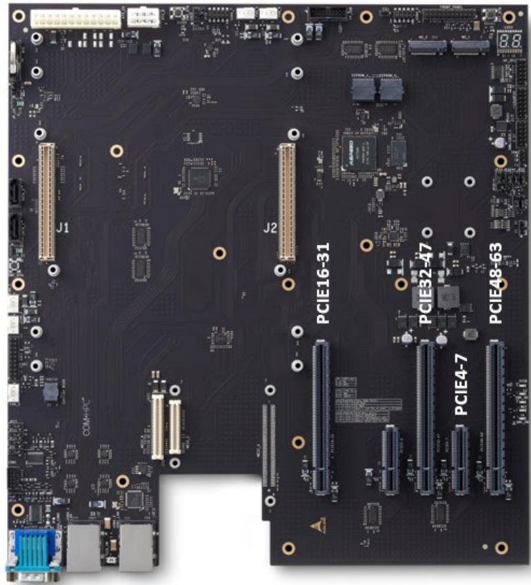
Maximum 2x FHFL PCI Express cards at PCIE16-31 slot and PCIE32-47 slot, and 1x FHHL PCI Express card at PCIE48-63 slot PCIE16-31 and PCIE32-47 slots can accommodate up to 2-slot-width PCI Express cards, in the condition of not using PCIE4-7 slot
![J1\nJ2\nPCIE16-31\nPCIE32-47\nPCIE4-7\nPCIE48-63\nCOM+PC](.com-hpc-server-base-manual-50m-77106-1000-10-230720/cb1d5cfa6ca96c451d5b74fd59d28b9ebba8468c0db3f6df6a680f44bdf08934.jpg)

Figure 1 – Carrier top view

# 2.2. Out-of-Band Management

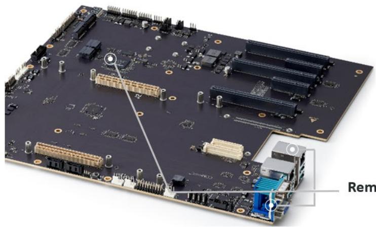
Out-of-band (OOB) management features, such as firmware update, power and reset control, performance monitoring and more, are defined by PICMG COM-HPC specifications.

The management architecture is divided into BMC (Board Management Controller, also called IPMI BMC or Carrier BMC) and MMC (Module Management Controller). As defined, BMC is located on the COM-HPC carrier, while MMC is located on the COM-HPC module.

Carrier BMC communicates with MMC through IPMB interface, an I2 C interface with IPMI protocol support.
![Close-up of a computer motherboard with visible components and a 'Rem' annotation (no readable text or symbols beyond label)](.com-hpc-server-base-manual-50m-77106-1000-10-230720/12e0aa61bd73672f199692ca8075ed098c609af72f249386b130bbd6eda250da.jpg)

# note/Local Managementby scenario

·IPMI BMC
Dedicate Ethernet forremote,VGAand COM portfor local

![The image displays a red-outlined icon of a document or piece of paper with a folded top-right corner. Inside the white area, there are two horizontal red lines stacked vertically, resembling an equals sign. This is a standard graphic symbol often used to represent a text file or document.](.com-hpc-server-base-manual-50m-77106-1000-10-230720/658b2b12dae0d53305fabdef9be12426ff04c7447e30c46016f24f031abb1a32.jpg)

Note: OOB management support and features are dependent on the module used.

# 2.3. High Speed Ethernet Expansion

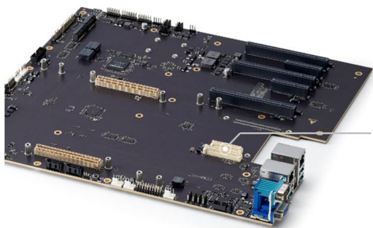
The high-speed Ethernet MACs are located on the COM-HPC module used. The PHY is (if used) located on the COM-HPC carrier as defined by PICMG COM-HPC specifications.

PHY may vary due to the silicon platform or Ethernet controller used, thus a connector-style design instead of a PHY chip on carrier is adopted for further expansion purposes.

OCP connector is adopted and supports dedicated OCP mezzanine card (by choice).
![Close-up of a computer motherboard with various electronic components and connectors (no visible text or symbols)](.com-hpc-server-base-manual-50m-77106-1000-10-230720/bc316cbc82ba836f2d5367dd39ec5b05cb7fc921ad04fa32f00404c66c17c7c0.jpg)

# High Speed Ethernet Expansion by choice

·OCP style Optical or Copper 10GbE

# 3. Component Location
![GP_SPI 12xGPIO\nSMB/I2C0,1 IPMI\nJP31\nJP32\nJP33\nJP35\nSW1\nBMC_DBG\nPWR_ON\n5VSB BMC_HB\nS3 WDT PCIE48-63\nPCIE4-7\nPCIE32-47\nPCIE0-3\nIPMI\nBMC\nA5T2500\nPCIE16-31\nJ2\nFAN_4\nFAN_5\nUSB6_7\nJP36\nCN35\nPWR_BTN\nUSB Hub\nUSB7206\nMEZZ_C\nMEZZ_B\nATX_8\nATX_24\nJ1\nRTC JP30 JP_S0 SATA0 SATA1 JP_S1 BMC_BTN FAN_1 FAN_2 ESPI FAN_0 JP27 JP28 JP29 JP9 COM1 JP34 VGA_COM0](.com-hpc-server-base-manual-50m-77106-1000-10-230720/32ddc6d387796b934eba9198ce7dc462c56529178314e49de44692a67af36903.jpg)

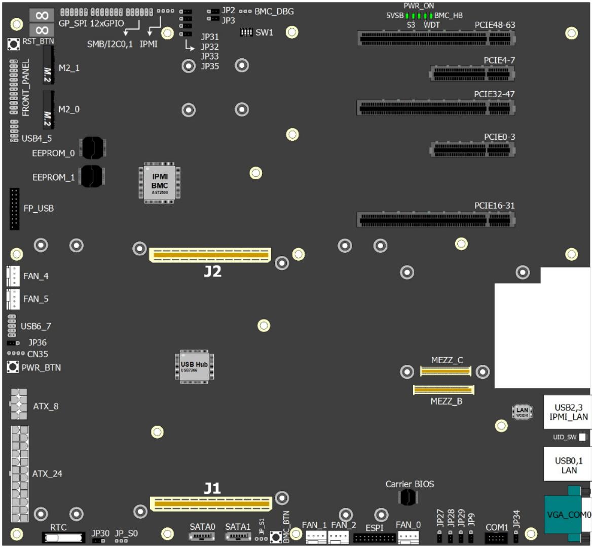
Figure 2 – Component location

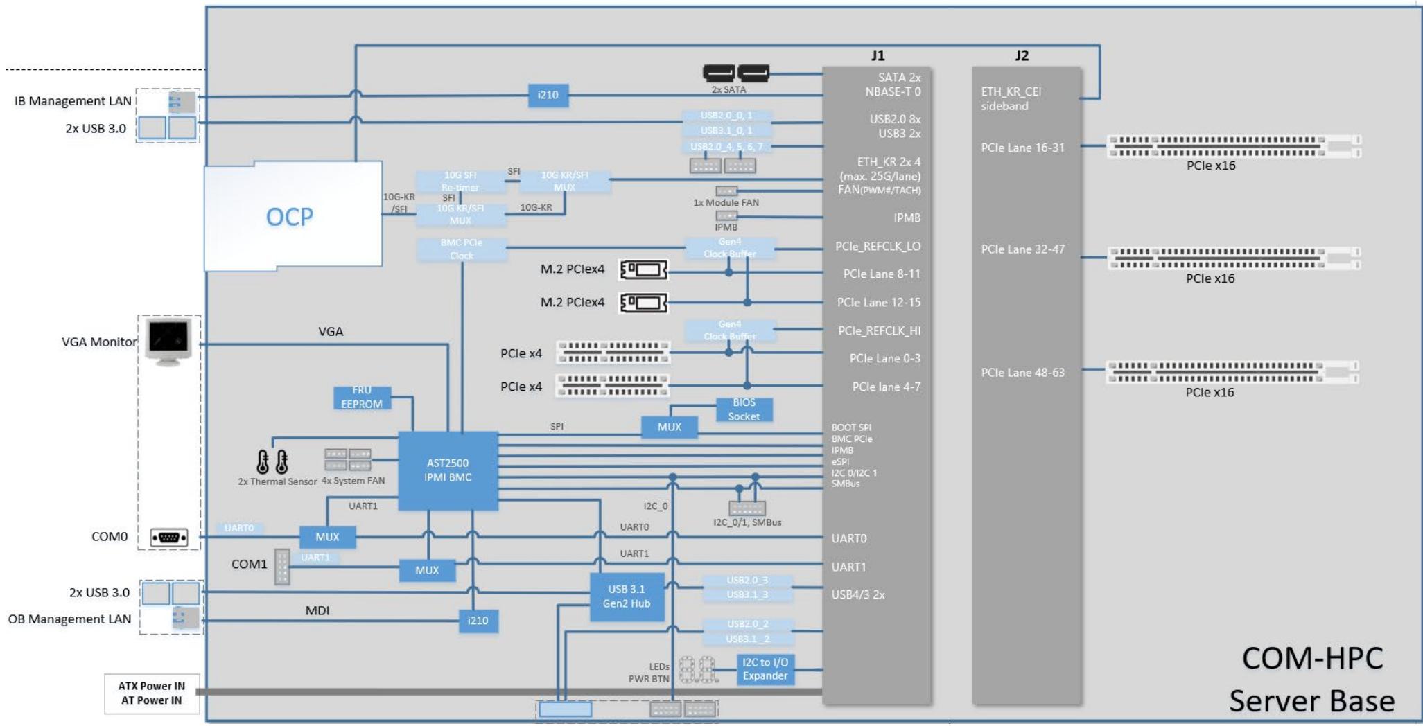
# 4. Functional Diagram
![**Labeled Blocks:**\n*   **OCP**\n*   **AST2500 IPMI BMC**\n*   **J1**\n*   **J2**\n*   **i210** (top and bottom instances)\n*   **M.2 PCle x4** (two instances)\n*   **PCIe x4** (two instances)\n*   **FRU EEPROM**\n*   **2x Thermal Sensor 4x System FAN**\n*   **MUX** (three instances)\n*   **USB 3.1 Gen2 Hub**\n*   **LEDs PWR BTN**\n*   **I2C to I/O Expander**\n*   **Gen4 Clock Buffer** (two instances)\n*   **BIOS Socket**\n*   **SPI**\n*   **10G SFI Re-timer SFI**\n*   **10G KR/SFI MUX**\n*   **BMC PCIe Clock**\n*   **2x SATA**\n*   **USB2.0_0, 1**\n*   **USB3.1_0, 1**\n*   **USB2.0_4, 5, 6, 7**\n*   **1x Module FAN**\n*   **IPMB** (two instances)\n*   **10G KR**\n*   **VGA Monitor**\n*   **COM0**\n*   **COM1**\n*   **IB Management LAN**\n*   **2x USB 3.0** (two instances)\n*   **OB Management LAN**\n*   **ATX Power IN AT Power IN**\n*   **PCIe x16** (three instances)\n*   **ETH_KR_CE1 sideband**\n*   **SATA 2x**\n*   **NBASE-T 0**\n*   **USB2.0 8x**\n*   **USB3 2x**\n*   **ETH_KR 2x 4 (max. 25G/lane)**\n*   **FAN(PWM#/TACH)**\n*   **PCIe_REFCLK_LO**\n*   **PCIe Lane 8-11**\n*   **PCIe Lane 12-15**\n*   **PCIe_REFCLK_HI**\n*   **PCIe Lane 0-3**\n*   **PCIe lane 4-7**\n*   **BOOT SPI**\n*   **BMC PCIe**\n*   **eSPI**\n*   **I2C 0/I2C 1**\n*   **SMBus**\n*   **UART0**\n*   **UART1**\n*   **USB4/3 2x**\n*   **USB2.0_3, USB3.1_3**\n*   **USB2.0_2, USB3.1_2**\n*   **COM-HPC Server Base**\n\n**Connections:**\n*   **OCP** connects to **i210**, **10G KR/SFI MUX**, **10G SFI Re-timer SFI**, **BMC PCIe Clock**, **VGA Monitor**, **IB Management LAN**, **2x USB 3.0**, and **ETH_KR_CE1 sideband** (via J2).\n*   **AST2500 IPMI BMC** connects to **FRU EEPROM**, **2x Thermal Sensor 4x System FAN**, **MUX** (UART1), **MUX** (UART0), **SPI**, **BMC PCIe Clock**, **USB 3.1 Gen2 Hub**, **I2C_0**, **UART0**, and **UART1**.\n*   **J1** connects to **2x SATA**, **i210** (via NBASE-T 0), **USB2.0_0, 1**, **USB3.1_0, 1**, **10G KR/SFI MUX** (via ETH_KR 2x 4), **1x Module FAN**, **IPMB**, **Gen4 Clock Buffer** (top), **M.2 PCle x4** (two instances), **Gen4 Clock Buffer** (bottom), **PCIe x4** (two instances), **SPI** (via BOOT SPI), **AST2500 IPMI BMC** (via multiple lines), and **USB 3.1 Gen2 Hub** (via USB4/3 2x).\n*   **J2** connects to **OCP**, **PCIe x16** (three instances).\n*   **USB 3.1 Gen2 Hub** connects to **USB2.0_3, USB3.1_3**, **USB2.0_2, USB3.1_2**, **I2C to I/O Expander**, and **LEDs PWR BTN**.\n*   **2x USB 3.0** (bottom left instance) connects to **USB 3.1 Gen2 Hub**.\n*   **OB Management LAN** connects to **i210** (bottom instance).\n*   **10G KR/SFI MUX** connects to **10G KR**, which connects to **10G SFI Re-timer SFI**.\n*   **SPI** connects to **BIOS Socket**, **MUX** (near BIOS), and **AST2500 IPMI BMC**.\n*   **ATX Power IN AT Power IN** provides power input to the system.](.com-hpc-server-base-manual-50m-77106-1000-10-230720/0679927327f4f0fe0bb1d93953437293a442e9b86ed02adced245dd67cb74d1d.jpg)

Figure 3 – Functional diagram

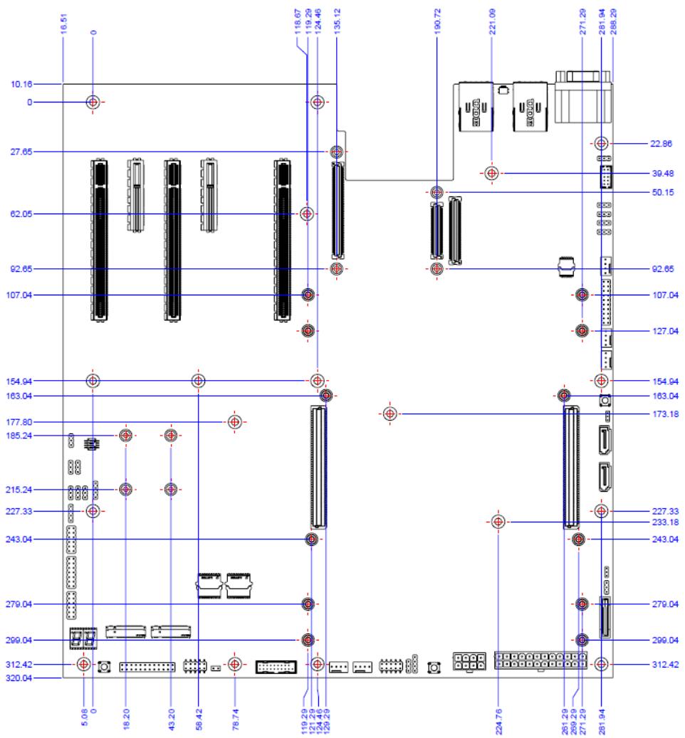
# 5. Mechanical Dimension
![| Component | Value  |\n| --------- | ------ |\n| Display   | 16.51  |\n| Computer  | 0      |\n| Tablet    | 118.67 |\n| Display   | 119.29 |\n| Tablet    | 124.46 |\n| Display   | 135.12 |\n| Tablet    | 190.72 |\n| Display   | 221.09 |\n| Display   | 271.29 |\n| Display   | 281.94 |\n| Display   | 288.29 |\n| Display   | 39.48  |\n| Display   | 50.15  |\n| Display   | 92.65  |\n| Display   | 107.04 |\n| Display   | 127.04 |\n| Display   | 154.94 |\n| Display   | 163.04 |\n| Display   | 173.18 |\n| Display   | 227.33 |\n| Display   | 233.18 |\n| Display   | 243.04 |\n| Display   | 279.04 |\n| Display   | 299.04 |\n| Display   | 312.42 |\n| Display   | 312.42 |\n| Computer  | 5.08   |\n| Tablet    | 0      |\n| Display   | 18.20  |\n| Tablet    | 43.20  |\n| Display   | 58.42  |\n| Display   | 78.74  |\n| Display   | 119.29 |\n| Display   | 124.46 |\n| Display   | 129.29 |\n| Display   | 224.76 |\n| Display   | 261.29 |\n| Display   | 269.29 |\n| Display   | 271.29 |\n| Display   | 281.94 |\n| Display   | 312.42 |\nThe chart displays the dimensions and component values of various electronic devices.](.com-hpc-server-base-manual-50m-77106-1000-10-230720/a5611b3c2088bef736cf33eb4db69e388c998e0c85d40bb0b1290b0b9e0de685.jpg)

Figure 4 – Mechanical dimensions

![The image displays a red-orange icon on a white background. It features a stylized representation of a document or page with a folded corner at the top right. Inside the document shape are three horizontal lines stacked vertically, resembling lines of text.](.com-hpc-server-base-manual-50m-77106-1000-10-230720/13b24aa06d8b3bf1a07fa4767ed957c58e1bd6fccbf293bbc08fff22cf94accc.jpg)

Note: All dimensions are shown in millimeters with a tolerance of ± 0.25mm unless otherwise noted.

# 6. Connectors and Pinouts

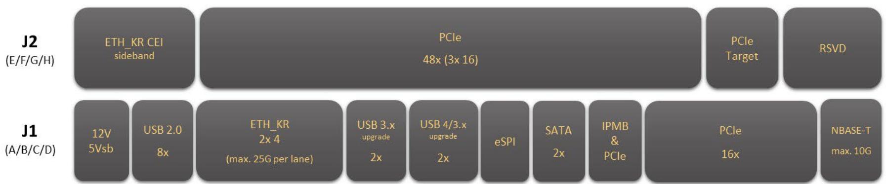
# 6.1. Carrier Board Signals — Server Type
![| Category | Label | Value |\n| -------- | ----- | ----- |\n| J2 (E/F/G/H) | ETH_KR CEI sideband | 48x (3x 16) |\n| J2 (E/F/G/H) | PCIe 48x | 48x (3x 16) |\n| J2 (E/F/G/H) | PCIe Target | - |\n| J2 (E/F/G/H) | RSVD | - |\n| J1 (A/B/C/D) | 12V 5Vsb | 12V |\n| J1 (A/B/C/D) | USB 2.0 8x | USB 2.0 |\n| J1 (A/B/C/D) | ETH_KR 2x 4 (max. 25G per lane) | 2x |\n| J1 (A/B/C/D) | USB 3.x upgrade | 2x |\n| J1 (A/B/C/D) | USB 4/3.x upgrade | 2x |\n| J1 (A/B/C/D) | eSPI | - |\n| J1 (A/B/C/D) | SATA 2x | - |\n| J1 (A/B/C/D) | IPMB & PCIe | - |\n| J1 (A/B/C/D) | PCIe 16x | - |\n| J1 (A/B/C/D) | NBASE-T max. 10G | - |](.com-hpc-server-base-manual-50m-77106-1000-10-230720/1a341af152791321066d62123b566a47eeb2cb1c7f9b36d31b487a7a4cdaf0d8.jpg)

Figure 5 – Carrier board signals, Server type pinout

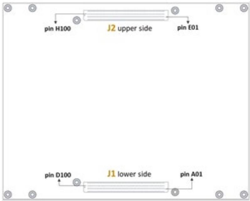
# 6.2. Connector Location and Pinout Compatibility

Connector positions and pinouts comply with pinout and signal descriptions within PICMG COM-HPC Carrier Design Guide R2. This document includes: descriptions of pinouts, signals, and mechanical characteristics of the COM-HPC specification. The COM-HPC Server Base carrier is compatible with COM-HPC modules in Size E and D form factor, Server Type pinout, COM-HPC Module Base Specification R1.0.
![pin H100\nJ2 upper side\npin E01\npin D100\nJ1 lower side\npin A01](.com-hpc-server-base-manual-50m-77106-1000-10-230720/dd90b2e63384e7667283dada3c28bd6669249b6eec78717aa8560b72d60cbdec.jpg)

Figure 6 – Connector location and pinout compatibility

# 6.3. Carrier Board Design

COM-HPC Server Base follows the PICMG COM-HPC Carrier Design Guide where possible, and its design and schematic have been fully verified. It is recommend to utilize them as references for your carrier board design. COM-HPC Server Base schematics and mechanical files, as well as the CDG, can be downloaded from ADLINK COM’s webpage.

# 6.4. COM-HPC Board-to-board Connectors

Signals and Pinouts for COM-HPC Server Type (Size D & E)

<table><tr><td colspan="2">Row A</td><td></td><td colspan="2">Row B</td><td></td><td colspan="2">Row C</td><td></td><td colspan="2">Row D</td></tr><tr><td>A1</td><td>VCC</td><td></td><td>B1</td><td>VCC</td><td></td><td>C1</td><td>VCC</td><td></td><td>D1</td><td>VCC</td></tr><tr><td>A2</td><td>VCC</td><td></td><td>B2</td><td>PWRBTN#</td><td></td><td>C2</td><td>RSTBTN#</td><td></td><td>D2</td><td>VCC</td></tr><tr><td>A3</td><td>VCC</td><td></td><td>B3</td><td>VCC</td><td></td><td>C3</td><td>VCC</td><td></td><td>D3</td><td>VCC</td></tr><tr><td>A4</td><td>VCC</td><td></td><td>B4</td><td>THERMTRIP#</td><td></td><td>C4</td><td>CARRIER_HOT#</td><td></td><td>D4</td><td>VCC</td></tr><tr><td>A5</td><td>VCC</td><td></td><td>B5</td><td>VCC</td><td></td><td>C5</td><td>VCC</td><td></td><td>D5</td><td>VCC</td></tr><tr><td>A6</td><td>VCC</td><td></td><td>B6</td><td>TAMPER#</td><td></td><td>C6</td><td>VIN_PWR_OK</td><td></td><td>D6</td><td>VCC</td></tr><tr><td>A7</td><td>VCC</td><td></td><td>B7</td><td>VCC</td><td></td><td>C7</td><td>VCC</td><td></td><td>D7</td><td>VCC</td></tr><tr><td>A8</td><td>VCC</td><td></td><td>B8</td><td>SUS_S3#</td><td></td><td>C8</td><td>SUS_S4_S5#</td><td></td><td>D8</td><td>VCC</td></tr><tr><td>A9</td><td>VCC</td><td></td><td>B9</td><td>VCC</td><td></td><td>C9</td><td>VCC</td><td></td><td>D9</td><td>VCC</td></tr><tr><td>A10</td><td>GND</td><td></td><td>B10</td><td>WD_STROBE#</td><td></td><td>C10</td><td>GND</td><td></td><td>D10</td><td>WAKE0#</td></tr><tr><td>A11</td><td>BATLOW#</td><td></td><td>B11</td><td>WD_OUT</td><td></td><td>C11</td><td>FAN_PWMOUT</td><td></td><td>D11</td><td>WAKE1#</td></tr><tr><td>A12</td><td>PLTRST#</td><td></td><td>B12</td><td>GND</td><td></td><td>C12</td><td>FAN_TACHIN</td><td></td><td>D12</td><td>GND</td></tr><tr><td>A13</td><td>GND</td><td></td><td>B13</td><td>USB5-</td><td></td><td>C13</td><td>GND</td><td></td><td>D13</td><td>USB1-</td></tr><tr><td>A14</td><td>USB7-</td><td></td><td>B14</td><td>USB5+</td><td></td><td>C14</td><td>USB3-</td><td></td><td>D14</td><td>USB1+</td></tr><tr><td>A15</td><td>USB7+</td><td></td><td>B15</td><td>GND</td><td></td><td>C15</td><td>USB3+</td><td></td><td>D15</td><td>GND</td></tr><tr><td>A16</td><td>GND</td><td></td><td>B16</td><td>USB4-</td><td></td><td>C16</td><td>GND</td><td></td><td>D16</td><td>USB0-</td></tr><tr><td>A17</td><td>USB6-</td><td></td><td>B17</td><td>USB4+</td><td></td><td>C17</td><td>USB2-</td><td></td><td>D17</td><td>USB0+</td></tr><tr><td>A18</td><td>USB6+</td><td></td><td>B18</td><td>GND</td><td></td><td>C18</td><td>USB2+</td><td></td><td>D18</td><td>GND</td></tr><tr><td>A19</td><td>GND</td><td></td><td>B19</td><td>RSVD</td><td></td><td>C19</td><td>GND</td><td></td><td>D19</td><td>ETH0_RX-</td></tr><tr><td>A20</td><td>ETH4_RX-</td><td></td><td>B20</td><td>RSVD</td><td></td><td>C20</td><td>ETH0_TX-</td><td></td><td>D20</td><td>ETH0_RX+</td></tr><tr><td>A21</td><td>ETH4_RX+</td><td></td><td>B21</td><td>RSVD</td><td></td><td>C21</td><td>ETH0_TX+</td><td></td><td>D21</td><td>GND</td></tr><tr><td>A22</td><td>GND</td><td></td><td>B22</td><td>RSVD</td><td></td><td>C22</td><td>GND</td><td></td><td>D22</td><td>ETH1_RX-</td></tr><tr><td>A23</td><td>ETH5_RX-</td><td></td><td>B23</td><td>RSVD</td><td></td><td>C23</td><td>ETH1_TX-</td><td></td><td>D23</td><td>ETH1_RX+</td></tr><tr><td>A24</td><td>ETH5_RX+</td><td></td><td>B24</td><td>VCC_5V_SBY</td><td></td><td>C24</td><td>ETH1_TX+</td><td></td><td>D24</td><td>GND</td></tr><tr><td>A25</td><td>GND</td><td></td><td>B25</td><td>USB67_OC#</td><td></td><td>C25</td><td>GND</td><td></td><td>D25</td><td>ETH2_RX-</td></tr><tr><td>A26</td><td>ETH6_RX-</td><td></td><td>B26</td><td>USB45_OC#</td><td></td><td>C26</td><td>ETH2_TX-</td><td></td><td>D26</td><td>ETH2_RX+</td></tr><tr><td>A27</td><td>ETH6_RX+</td><td></td><td>B27</td><td>USB23_OC#</td><td></td><td>C27</td><td>ETH2_TX+</td><td></td><td>D27</td><td>GND</td></tr><tr><td>A28</td><td>GND</td><td></td><td>B28</td><td>USB01_OC#</td><td></td><td>C28</td><td>GND</td><td></td><td>D28</td><td>ETH3_RX-</td></tr><tr><td>A29</td><td>ETH7_RX-</td><td></td><td>B29</td><td>SML1_CLK</td><td></td><td>C29</td><td>ETH3_TX-</td><td></td><td>D29</td><td>ETH3_RX+</td></tr><tr><td>A30</td><td>ETH7_RX+</td><td></td><td>B30</td><td>SML1_DAT</td><td></td><td>C30</td><td>ETH3_TX+</td><td></td><td>D30</td><td>GND</td></tr><tr><td>A31</td><td>GND</td><td></td><td>B31</td><td>PMCALERT#</td><td></td><td>C31</td><td>GND</td><td></td><td>D31</td><td>USB3_SSTX-</td></tr><tr><td>A32</td><td>RSVD</td><td></td><td>B32</td><td>SML0_CLK</td><td></td><td>C32</td><td>USB3_SSRX-</td><td></td><td>D32</td><td>USB3_SSTX+</td></tr><tr><td>A33</td><td>RSVD</td><td></td><td>B33</td><td>SML0_DAT</td><td></td><td>C33</td><td>USB3_SSRX+</td><td></td><td>D33</td><td>GND</td></tr><tr><td>A34</td><td>GND</td><td></td><td>B34</td><td>USB_PD_ALERT#</td><td></td><td>C34</td><td>GND</td><td></td><td>D34</td><td>USB2_SSTX-</td></tr><tr><td>A35</td><td>ETH4_TX-</td><td></td><td>B35</td><td>USB_PD_I2C_CLK</td><td></td><td>C35</td><td>USB2_SSRX-</td><td></td><td>D35</td><td>USB2_SSTX+</td></tr><tr><td>A36</td><td>ETH4_TX+</td><td></td><td>B36</td><td>USB_PD_I2C_DAT</td><td></td><td>C36</td><td>USB2_SSRX+</td><td></td><td>D36</td><td>GND</td></tr><tr><td>A37</td><td>GND</td><td></td><td>B37</td><td>USB_RT_ENA</td><td></td><td>C37</td><td>GND</td><td></td><td>D37</td><td>USB1_SSTX0-</td></tr><tr><td>A38</td><td>ETH5_TX-</td><td></td><td>B38</td><td>USB1_LSRX</td><td></td><td>C38</td><td>USB1_SSRX0-</td><td></td><td>D38</td><td>USB1_SSTX0+</td></tr><tr><td>A39</td><td>ETH5_TX+</td><td></td><td>B39</td><td>USB1_LSTX</td><td></td><td>C39</td><td>USB1_SSRX0+</td><td></td><td>D39</td><td>GND</td></tr><tr><td>A40</td><td>GND</td><td></td><td>B40</td><td>USB0_LSRX</td><td></td><td>C40</td><td>GND</td><td></td><td>D40</td><td>USB1_SSTX1-</td></tr><tr><td>A41</td><td>ETH6_TX-</td><td></td><td>B41</td><td>USB0_LSTX</td><td></td><td>C41</td><td>USB1_SSRX1-</td><td></td><td>D41</td><td>USB1_SSTX1+</td></tr><tr><td>A42</td><td>ETH6_TX+</td><td></td><td>B42</td><td>GND</td><td></td><td>C42</td><td>USB1_SSRX1+</td><td></td><td>D42</td><td>GND</td></tr><tr><td>A43</td><td>GND</td><td></td><td>B43</td><td>USB0_AUX-</td><td></td><td>C43</td><td>GND</td><td></td><td>D43</td><td>USB0_SSTX0-</td></tr><tr><td>A44</td><td>ETH7_TX-</td><td></td><td>B44</td><td>USB0_AUX+</td><td></td><td>C44</td><td>USB0_SSRX0-</td><td></td><td>D44</td><td>USB0_SSTX0+</td></tr><tr><td>A45</td><td>ETH7_TX+</td><td></td><td>B45</td><td>RSVD</td><td></td><td>C45</td><td>USB0_SSRX0+</td><td></td><td>D45</td><td>GND</td></tr><tr><td>A46</td><td>GND</td><td></td><td>B46</td><td>RSVD</td><td></td><td>C46</td><td>GND</td><td></td><td>D46</td><td>USB0_SSTX1-</td></tr><tr><td>A47</td><td>USB1_AUX-</td><td></td><td>B47</td><td>VCC_BOOT_SPI</td><td></td><td>C47</td><td>USB0_SSRX1-</td><td></td><td>D47</td><td>USB0_SSTX1+</td></tr><tr><td>A48</td><td>USB1_AUX+</td><td></td><td>B48</td><td>BOOT_SPI_CS#</td><td></td><td>C48</td><td>USB0_SSRX1+</td><td></td><td>D48</td><td>GND</td></tr><tr><td>A49</td><td>GND</td><td></td><td>B49</td><td>BSEL0</td><td></td><td>C49</td><td>GND</td><td></td><td>D49</td><td>SATA0_RX-</td></tr><tr><td>A50</td><td>eSPI_IO0</td><td></td><td>B50</td><td>BSEL1</td><td></td><td>C50</td><td>BOOT_SPI_IO0</td><td></td><td>D50</td><td>SATA0_RX+</td></tr><tr><td>A51</td><td>eSPI_IO1</td><td></td><td>B51</td><td>BSEL2</td><td></td><td>C51</td><td>BOOT_SPI_IO1</td><td></td><td>D51</td><td>GND</td></tr><tr><td>A52</td><td>eSPI_IO2</td><td></td><td>B52</td><td>eSPI_ALERT0#</td><td></td><td>C52</td><td>BOOT_SPI_IO2</td><td></td><td>D52</td><td>SATA0_TX-</td></tr><tr><td>A53</td><td>eSPI_IO3</td><td></td><td>B53</td><td>eSPI_ALERT1#</td><td></td><td>C53</td><td>BOOT_SPI_IO3</td><td></td><td>D53</td><td>SATA0_TX+</td></tr><tr><td>A54</td><td>eSPI_CLK</td><td></td><td>B54</td><td>eSPI_CS0#</td><td></td><td>C54</td><td>BOOT_SPI_CLK</td><td></td><td>D54</td><td>GND</td></tr><tr><td>A55</td><td>GND</td><td></td><td>B55</td><td>eSPI_CS1#</td><td></td><td>C55</td><td>GND</td><td></td><td>D55</td><td>SATA1_RX-</td></tr><tr><td>A56</td><td>PCIe_CLKREQ0_LO#</td><td></td><td>B56</td><td>eSPI_RST#</td><td></td><td>C56</td><td>PCIe_REFCLK0_HI-</td><td></td><td>D56</td><td>SATA1_RX+</td></tr><tr><td>A57</td><td>PCIe_CLKREQ0_HI#</td><td></td><td>B57</td><td>GND</td><td></td><td>C57</td><td>PCIe_REFCLK0_HI+</td><td></td><td>D57</td><td>GND</td></tr><tr><td>A58</td><td>GND</td><td></td><td>B58</td><td>PCIe_BMC_RX-</td><td></td><td>C58</td><td>GND</td><td></td><td>D58</td><td>SATA1_TX-</td></tr><tr><td>A59</td><td>PCIe_BMC_TX-</td><td></td><td>B59</td><td>PCIe_BMC_RX+</td><td></td><td>C59</td><td>PCIe_REFCLK0_LO-</td><td></td><td>D59</td><td>SATA1_TX+</td></tr><tr><td>A60</td><td>PCIe_BMC_TX+</td><td></td><td>B60</td><td>GND</td><td></td><td>C60</td><td>PCIe_REFCLK0_LO+</td><td></td><td>D60</td><td>GND</td></tr><tr><td>A61</td><td>GND</td><td></td><td>B61</td><td>PCIe08_RX-</td><td></td><td>C61</td><td>GND</td><td></td><td>D61</td><td>PCIe00_TX-</td></tr><tr><td>A62</td><td>PCIe08_TX-</td><td></td><td>B62</td><td>PCIe08_RX+</td><td></td><td>C62</td><td>PCIe00_RX-</td><td></td><td>D62</td><td>PCIe00_TX+</td></tr><tr><td>A63</td><td>PCIe08_TX+</td><td></td><td>B63</td><td>GND</td><td></td><td>C63</td><td>PCIe00_RX+</td><td></td><td>D63</td><td>GND</td></tr><tr><td>A64</td><td>GND</td><td></td><td>B64</td><td>PCIe09_RX-</td><td></td><td>C64</td><td>GND</td><td></td><td>D64</td><td>PCIe01_TX-</td></tr><tr><td>A65</td><td>PCIe09_TX-</td><td></td><td>B65</td><td>PCIe09_RX+</td><td></td><td>C65</td><td>PCIe01_RX-</td><td></td><td>D65</td><td>PCIe01_TX+</td></tr><tr><td>A66</td><td>PCIe09_TX+</td><td></td><td>B66</td><td>GND</td><td></td><td>C66</td><td>PCIe01_RX+</td><td></td><td>D66</td><td>GND</td></tr><tr><td>A67</td><td>GND</td><td></td><td>B67</td><td>PCIe10_RX-</td><td></td><td>C67</td><td>GND</td><td></td><td>D67</td><td>PCIe02_TX-</td></tr><tr><td>A68</td><td>PCIe10_TX-</td><td></td><td>B68</td><td>PCIe10_RX+</td><td></td><td>C68</td><td>PCIe02_RX-</td><td></td><td>D68</td><td>PCIe02_TX+</td></tr><tr><td>A69</td><td>PCIe10_TX+</td><td></td><td>B69</td><td>GND</td><td></td><td>C69</td><td>PCIe02_RX+</td><td></td><td>D69</td><td>GND</td></tr><tr><td>A70</td><td>GND</td><td></td><td>B70</td><td>PCIe11_RX-</td><td></td><td>C70</td><td>GND</td><td></td><td>D70</td><td>PCIe03_TX-</td></tr><tr><td>A71</td><td>PCIe11_TX-</td><td></td><td>B71</td><td>PCIe11_RX+</td><td></td><td>C71</td><td>PCIe03_RX-</td><td></td><td>D71</td><td>PCIe03_TX+</td></tr><tr><td>A72</td><td>PCIe11_TX+</td><td></td><td>B72</td><td>GND</td><td></td><td>C72</td><td>PCIe03_RX+</td><td></td><td>D72</td><td>GND</td></tr><tr><td>A73</td><td>GND</td><td></td><td>B73</td><td>PCIe12_RX-</td><td></td><td>C73</td><td>GND</td><td></td><td>D73</td><td>PCIe04_TX-</td></tr><tr><td>A74</td><td>PCIe12_TX-</td><td></td><td>B74</td><td>PCIe12_RX+</td><td></td><td>C74</td><td>PCIe04_RX-</td><td></td><td>D74</td><td>PCIe04_TX+</td></tr><tr><td>A75</td><td>PCIe12_TX+</td><td></td><td>B75</td><td>GND</td><td></td><td>C75</td><td>PCIe04_RX+</td><td></td><td>D75</td><td>GND</td></tr><tr><td>A76</td><td>GND</td><td></td><td>B76</td><td>PCIe13_RX-</td><td></td><td>C76</td><td>GND</td><td></td><td>D76</td><td>PCIe05_TX-</td></tr><tr><td>A77</td><td>PCIe13_TX-</td><td></td><td>B77</td><td>PCIe13_RX+</td><td></td><td>C77</td><td>PCIe05_RX-</td><td></td><td>D77</td><td>PCIe05_TX+</td></tr><tr><td>A78</td><td>PCIe13_TX+</td><td></td><td>B78</td><td>GND</td><td></td><td>C78</td><td>PCIe05_RX+</td><td></td><td>D78</td><td>GND</td></tr><tr><td>A79</td><td>GND</td><td></td><td>B79</td><td>PCIe14_RX-</td><td></td><td>C79</td><td>GND</td><td></td><td>D79</td><td>PCIe06_TX-</td></tr><tr><td>A80</td><td>PCIe14_TX-</td><td></td><td>B80</td><td>PCIe14_RX+</td><td></td><td>C80</td><td>PCIe06_RX-</td><td></td><td>D80</td><td>PCIe06_TX+</td></tr><tr><td>A81</td><td>PCIe14_TX+</td><td></td><td>B81</td><td>GND</td><td></td><td>C81</td><td>PCIe06_RX+</td><td></td><td>D81</td><td>GND</td></tr><tr><td>A82</td><td>GND</td><td></td><td>B82</td><td>PCIe15_RX-</td><td></td><td>C82</td><td>GND</td><td></td><td>D82</td><td>PCIe07_TX-</td></tr><tr><td>A83</td><td>PCIe15_TX-</td><td></td><td>B83</td><td>PCIe15_RX+</td><td></td><td>C83</td><td>PCIe07_RX-</td><td></td><td>D83</td><td>PCIe07_TX+</td></tr><tr><td>A84</td><td>PCIe15_TX+</td><td></td><td>B84</td><td>GND</td><td></td><td>C84</td><td>PCIe07_RX+</td><td></td><td>D84</td><td>GND</td></tr><tr><td>A85</td><td>GND</td><td></td><td>B85</td><td>RSVD</td><td></td><td>C85</td><td>GND</td><td></td><td>D85</td><td>NBASET0_MD10-</td></tr><tr><td>A86</td><td>VCC_RTC</td><td></td><td>B86</td><td>RSMRST_OUT#</td><td></td><td>C86</td><td>SMB_CLK</td><td></td><td>D86</td><td>NBASET0_MD10+</td></tr><tr><td>A87</td><td>SUS_CLK</td><td></td><td>B87</td><td>UART1_TX</td><td></td><td>C87</td><td>SMB_DAT</td><td></td><td>D87</td><td>GND</td></tr><tr><td>A88</td><td>GPIO_00</td><td></td><td>B88</td><td>UART1_RX</td><td></td><td>C88</td><td>SMB_ALERT#</td><td></td><td>D88</td><td>NBASET0_MD11-</td></tr><tr><td>A89</td><td>GPIO_01</td><td></td><td>B89</td><td>UART1_RTS#</td><td></td><td>C89</td><td>UART0_TX</td><td></td><td>D89</td><td>NBASET0_MD11+</td></tr><tr><td>A90</td><td>GPIO_02</td><td></td><td>B90</td><td>UART1_CTS#</td><td></td><td>C90</td><td>UART0_RX</td><td></td><td>D90</td><td>GND</td></tr><tr><td>A91</td><td>GPIO_03</td><td></td><td>B91</td><td>IPMB_CLK</td><td></td><td>C91</td><td>UART0_RTS#</td><td></td><td>D91</td><td>NBASET0_MD12-</td></tr><tr><td>A92</td><td>GPIO_04</td><td></td><td>B92</td><td>IPMB_DAT</td><td></td><td>C92</td><td>UART0_CTS#</td><td></td><td>D92</td><td>NBASET0_MD12+</td></tr><tr><td>A93</td><td>GPIO_05</td><td></td><td>B93</td><td>GPSPI_MOSI</td><td></td><td>C93</td><td>I2C0_CLK</td><td></td><td>D93</td><td>GND</td></tr><tr><td>A94</td><td>GPIO_06</td><td></td><td>B94</td><td>GPSPI_MISO</td><td></td><td>C94</td><td>I2C0_DAT</td><td></td><td>D94</td><td>NBASET0_MD13-</td></tr><tr><td>A95</td><td>GPIO_07</td><td></td><td>B95</td><td>GPSPI_CS0#</td><td></td><td>C95</td><td>I2C0_ALERT#</td><td></td><td>D95</td><td>NBASET0_MD13+</td></tr><tr><td>A96</td><td>GPIO_08</td><td></td><td>B96</td><td>GPSPI_CS1#</td><td></td><td>C96</td><td>I2C1_CLK</td><td></td><td>D96</td><td>GND</td></tr><tr><td>A97</td><td>GPIO_09</td><td></td><td>B97</td><td>GPSP1_CS2#</td><td></td><td>C97</td><td>I2C1_DAT</td><td></td><td>D97</td><td>NBASET0_LINK_MAX#</td></tr><tr><td>A98</td><td>GPIO_10</td><td></td><td>B98</td><td>GPSP1_CS3#</td><td></td><td>C98</td><td>NBASET0_SDP</td><td></td><td>D98</td><td>NBASET0_LINK_MID#</td></tr><tr><td>A99</td><td>GPIO_11</td><td></td><td>B99</td><td>GPSP1_CLK</td><td></td><td>C99</td><td>NBASET0_CTREF</td><td></td><td>D99</td><td>NBASET0_LINK_ACT#</td></tr><tr><td>A100</td><td>TYPE0</td><td></td><td>B100</td><td>GPSP1_ALERT#</td><td></td><td>C100</td><td>TYPE1</td><td></td><td>D100</td><td>TYPE2</td></tr></table>

<table><tr><td colspan="2">Row E</td><td></td><td colspan="2">Row F</td><td></td><td colspan="2">Row G</td><td></td><td colspan="2">Row H</td></tr><tr><td>E1</td><td>RAPID_SHUTDOWN</td><td></td><td>F1</td><td>ETH2_SDP</td><td></td><td>G1</td><td>VCC_5V_SBY</td><td></td><td>H1</td><td>RSVD</td></tr><tr><td>E2</td><td>GND</td><td></td><td>F2</td><td>ETH3_SDP</td><td></td><td>G2</td><td>RSVD</td><td></td><td>H2</td><td>RSVD</td></tr><tr><td>E3</td><td>RSVD</td><td></td><td>F3</td><td>ETH4_SDP</td><td></td><td>G3</td><td>RSVD</td><td></td><td>H3</td><td>RSVD</td></tr><tr><td>E4</td><td>RSVD</td><td></td><td>F4</td><td>ETH5_SDP</td><td></td><td>G4</td><td>RSVD</td><td></td><td>H4</td><td>RSVD</td></tr><tr><td>E5</td><td>GND</td><td></td><td>F5</td><td>ETH6_SDP</td><td></td><td>G5</td><td>RSVD</td><td></td><td>H5</td><td>RSVD</td></tr><tr><td>E6</td><td>RSVD</td><td></td><td>F6</td><td>ETH7_SDP</td><td></td><td>G6</td><td>RSVD</td><td></td><td>H6</td><td>RSVD</td></tr><tr><td>E7</td><td>RSVD</td><td></td><td>F7</td><td>ETH4-7_I2C_CLK</td><td></td><td>G7</td><td>RSVD</td><td></td><td>H7</td><td>RSVD</td></tr><tr><td>E8</td><td>GND</td><td></td><td>F8</td><td>ETH4-7_I2C_DAT</td><td></td><td>G8</td><td>RSVD</td><td></td><td>H8</td><td>RSVD</td></tr><tr><td>E9</td><td>RSVD</td><td></td><td>F9</td><td>ETH4-7_INT#</td><td></td><td>G9</td><td>RSVD</td><td></td><td>H9</td><td>RSVD</td></tr><tr><td>E10</td><td>RSVD</td><td></td><td>F10</td><td>ETH4-7_MDIO_CLK</td><td></td><td>G10</td><td>RSVD</td><td></td><td>H10</td><td>RSVD</td></tr><tr><td>E11</td><td>GND</td><td></td><td>F11</td><td>ETH4-7_MDIO_DAT</td><td></td><td>G11</td><td>RSVD</td><td></td><td>H11</td><td>RSVD</td></tr><tr><td>E12</td><td>RSVD</td><td></td><td>F12</td><td>ETH4-7_PHY_INT#</td><td></td><td>G12</td><td>RSVD</td><td></td><td>H12</td><td>RSVD</td></tr><tr><td>E13</td><td>RSVD</td><td></td><td>F13</td><td>ETH4-7_PHY_RST#</td><td></td><td>G13</td><td>RSVD</td><td></td><td>H13</td><td>RSVD</td></tr><tr><td>E14</td><td>GND</td><td></td><td>F14</td><td>ETH4-7_PRSNT#</td><td></td><td>G14</td><td>GND</td><td></td><td>H14</td><td>RSVD</td></tr><tr><td>E15</td><td>RSVD</td><td></td><td>F15</td><td>RSVD</td><td></td><td>G15</td><td>RSVD</td><td></td><td>H15</td><td>RSVD</td></tr><tr><td>E16</td><td>RSVD</td><td></td><td>F16</td><td>RSVD</td><td></td><td>G16</td><td>RSVD</td><td></td><td>H16</td><td>RSVD</td></tr><tr><td>E17</td><td>GND</td><td></td><td>F17</td><td>RSVD</td><td></td><td>G17</td><td>RSVD</td><td></td><td>H17</td><td>RSVD</td></tr><tr><td>E18</td><td>RSVD</td><td></td><td>F18</td><td>RSVD</td><td></td><td>G18</td><td>RSVD</td><td></td><td>H18</td><td>RSVD</td></tr><tr><td>E19</td><td>RSVD</td><td></td><td>F19</td><td>GND</td><td></td><td>G19</td><td>RSVD</td><td></td><td>H19</td><td>GND</td></tr><tr><td>E20</td><td>GND</td><td></td><td>F20</td><td>PCIe32_RX-</td><td></td><td>G20</td><td>GND</td><td></td><td>H20</td><td>PCIe40_TX-</td></tr><tr><td>E21</td><td>PCIe32_TX-</td><td></td><td>F21</td><td>PCIe32_RX+</td><td></td><td>G21</td><td>PCIe40_RX-</td><td></td><td>H21</td><td>PCIe40_TX+</td></tr><tr><td>E22</td><td>PCIe32_TX+</td><td></td><td>F22</td><td>GND</td><td></td><td>G22</td><td>PCIe40_RX+</td><td></td><td>H22</td><td>GND</td></tr><tr><td>E23</td><td>GND</td><td></td><td>F23</td><td>PCIe33_RX-</td><td></td><td>G23</td><td>GND</td><td></td><td>H23</td><td>PCIe41_TX-</td></tr><tr><td>E24</td><td>PCIe33_TX-</td><td></td><td>F24</td><td>PCIe33_RX+</td><td></td><td>G24</td><td>PCIe41_RX-</td><td></td><td>H24</td><td>PCIe41_TX+</td></tr><tr><td>E25</td><td>PCIe33_TX+</td><td></td><td>F25</td><td>GND</td><td></td><td>G25</td><td>PCIe41_RX+</td><td></td><td>H25</td><td>GND</td></tr><tr><td>E26</td><td>GND</td><td></td><td>F26</td><td>PCIe34_RX-</td><td></td><td>G26</td><td>GND</td><td></td><td>H26</td><td>PCIe42_TX-</td></tr><tr><td>E27</td><td>PCIe34_TX-</td><td></td><td>F27</td><td>PCIe34_RX+</td><td></td><td>G27</td><td>PCIe42_RX-</td><td></td><td>H27</td><td>PCIe42_TX+</td></tr><tr><td>E28</td><td>PCIe34_TX+</td><td></td><td>F28</td><td>GND</td><td></td><td>G28</td><td>PCIe42_RX+</td><td></td><td>H28</td><td>GND</td></tr><tr><td>E29</td><td>GND</td><td></td><td>F29</td><td>PCIe35_RX-</td><td></td><td>G29</td><td>GND</td><td></td><td>H29</td><td>PCIe43_TX-</td></tr><tr><td>E30</td><td>PCIe35_TX-</td><td></td><td>F30</td><td>PCIe35_RX+</td><td></td><td>G30</td><td>PCIe43_RX-</td><td></td><td>H30</td><td>PCIe43_TX+</td></tr><tr><td>E31</td><td>PCIe35_TX+</td><td></td><td>F31</td><td>GND</td><td></td><td>G31</td><td>PCIe43_RX+</td><td></td><td>H31</td><td>GND</td></tr><tr><td>E32</td><td>GND</td><td></td><td>F32</td><td>PCIe36_RX-</td><td></td><td>G32</td><td>GND</td><td></td><td>H32</td><td>PCIe44_TX-</td></tr><tr><td>E33</td><td>PCIe36_TX-</td><td></td><td>F33</td><td>PCIe36_RX+</td><td></td><td>G33</td><td>PCIe44_RX-</td><td></td><td>H33</td><td>PCIe44_TX+</td></tr><tr><td>E34</td><td>PCIe36_TX+</td><td></td><td>F34</td><td>GND</td><td></td><td>G34</td><td>PCIe44_RX+</td><td></td><td>H34</td><td>GND</td></tr><tr><td>E35</td><td>GND</td><td></td><td>F35</td><td>PCIe37_RX-</td><td></td><td>G35</td><td>GND</td><td></td><td>H35</td><td>PCIe45_TX-</td></tr><tr><td>E36</td><td>PCIe37_TX-</td><td></td><td>F36</td><td>PCIe37_RX+</td><td></td><td>G36</td><td>PCIe45_RX-</td><td></td><td>H36</td><td>PCIe45_TX+</td></tr><tr><td>E37</td><td>PCIe37_TX+</td><td></td><td>F37</td><td>GND</td><td></td><td>G37</td><td>PCIe45_RX+</td><td></td><td>H37</td><td>GND</td></tr><tr><td>E38</td><td>GND</td><td></td><td>F38</td><td>PCIe38_RX-</td><td></td><td>G38</td><td>GND</td><td></td><td>H38</td><td>PCIe46_TX-</td></tr><tr><td>E39</td><td>PCIe38_TX-</td><td></td><td>F39</td><td>PCIe38_RX+</td><td></td><td>G39</td><td>PCIe46_RX-</td><td></td><td>H39</td><td>PCIe46_TX+</td></tr><tr><td>E40</td><td>PCIe38_TX+</td><td></td><td>F40</td><td>GND</td><td></td><td>G40</td><td>PCIe46_RX+</td><td></td><td>H40</td><td>GND</td></tr><tr><td>E41</td><td>GND</td><td></td><td>F41</td><td>PCIe39_RX-</td><td></td><td>G41</td><td>GND</td><td></td><td>H41</td><td>PCIe47_TX-</td></tr><tr><td>E42</td><td>PCIe39_TX-</td><td></td><td>F42</td><td>PCIe39_RX+</td><td></td><td>G42</td><td>PCIe47_RX-</td><td></td><td>H42</td><td>PCIe47_TX+</td></tr><tr><td>E43</td><td>PCIe39_TX+</td><td></td><td>F43</td><td>GND</td><td></td><td>G43</td><td>PCIe47_RX+</td><td></td><td>H43</td><td>GND</td></tr><tr><td>E44</td><td>GND</td><td></td><td>F44</td><td>PCIe16_RX-</td><td></td><td>G44</td><td>GND</td><td></td><td>H44</td><td>PCIe24_TX-</td></tr><tr><td>E45</td><td>PCIe16_TX-</td><td></td><td>F45</td><td>PCIe16_RX+</td><td></td><td>G45</td><td>PCIe24_RX-</td><td></td><td>H45</td><td>PCIe24_TX+</td></tr><tr><td>E46</td><td>PCIe16_TX+</td><td></td><td>F46</td><td>GND</td><td></td><td>G46</td><td>PCIe24_RX+</td><td></td><td>H46</td><td>GND</td></tr><tr><td>E47</td><td>GND</td><td></td><td>F47</td><td>PCIe17_RX-</td><td></td><td>G47</td><td>GND</td><td></td><td>H47</td><td>PCIe25_TX-</td></tr><tr><td>E48</td><td>PCIe17_TX-</td><td></td><td>F48</td><td>PCIe17_RX+</td><td></td><td>G48</td><td>PCIe25_RX-</td><td></td><td>H48</td><td>PCIe25_TX+</td></tr><tr><td>E49</td><td>PCIe17_TX+</td><td></td><td>F49</td><td>GND</td><td></td><td>G49</td><td>PCIe25_RX+</td><td></td><td>H49</td><td>GND</td></tr><tr><td>E50</td><td>GND</td><td></td><td>F50</td><td>PCIe18_RX-</td><td></td><td>G50</td><td>GND</td><td></td><td>H50</td><td>PCIe26_TX-</td></tr><tr><td>E51</td><td>PCIe18_TX-</td><td></td><td>F51</td><td>PCIe18_RX+</td><td></td><td>G51</td><td>PCIe26_RX-</td><td></td><td>H51</td><td>PCIe26_TX+</td></tr><tr><td>E52</td><td>PCIe18_TX+</td><td></td><td>F52</td><td>GND</td><td></td><td>G52</td><td>PCIe26_RX+</td><td></td><td>H52</td><td>GND</td></tr><tr><td>E53</td><td>GND</td><td></td><td>F53</td><td>PCIe19_RX-</td><td></td><td>G53</td><td>GND</td><td></td><td>H53</td><td>PCIe27_TX-</td></tr><tr><td>E54</td><td>PCIe19_TX-</td><td></td><td>F54</td><td>PCIe19_RX+</td><td></td><td>G54</td><td>PCIe27_RX-</td><td></td><td>H54</td><td>PCIe27_TX+</td></tr><tr><td>E55</td><td>PCIe19_TX+</td><td></td><td>F55</td><td>GND</td><td></td><td>G55</td><td>PCIe27_RX+</td><td></td><td>H55</td><td>GND</td></tr><tr><td>E56</td><td>GND</td><td></td><td>F56</td><td>PCIe20_RX-</td><td></td><td>G56</td><td>GND</td><td></td><td>H56</td><td>PCIe28_TX-</td></tr><tr><td>E57</td><td>PCIe20_TX-</td><td></td><td>F57</td><td>PCIe20_RX+</td><td></td><td>G57</td><td>PCIe28_RX-</td><td></td><td>H57</td><td>PCIe28_TX+</td></tr><tr><td>E58</td><td>PCIe20_TX+</td><td></td><td>F58</td><td>GND</td><td></td><td>G58</td><td>PCIe28_RX+</td><td></td><td>H58</td><td>GND</td></tr><tr><td>E59</td><td>GND</td><td></td><td>F59</td><td>PCIe21_RX-</td><td></td><td>G59</td><td>GND</td><td></td><td>H59</td><td>PCIe29_TX-</td></tr><tr><td>E60</td><td>PCIe21_TX-</td><td></td><td>F60</td><td>PCIe21_RX+</td><td></td><td>G60</td><td>PCIe29_RX-</td><td></td><td>H60</td><td>PCIe29_TX+</td></tr><tr><td>E61</td><td>PCIe21_TX+</td><td></td><td>F61</td><td>GND</td><td></td><td>G61</td><td>PCIe29_RX+</td><td></td><td>H61</td><td>GND</td></tr><tr><td>E62</td><td>GND</td><td></td><td>F62</td><td>PCIe22_RX-</td><td></td><td>G62</td><td>GND</td><td></td><td>H62</td><td>PCIe30_TX-</td></tr><tr><td>E63</td><td>PCIe22_TX-</td><td></td><td>F63</td><td>PCIe22_RX+</td><td></td><td>G63</td><td>PCIe30_RX-</td><td></td><td>H63</td><td>PCIe30_TX+</td></tr><tr><td>E64</td><td>PCIe22_TX+</td><td></td><td>F64</td><td>GND</td><td></td><td>G64</td><td>PCIe30_RX+</td><td></td><td>H64</td><td>GND</td></tr><tr><td>E65</td><td>GND</td><td></td><td>F65</td><td>PCIe23_RX-</td><td></td><td>G65</td><td>GND</td><td></td><td>H65</td><td>PCIe31_TX-</td></tr><tr><td>E66</td><td>PCIe23_TX-</td><td></td><td>F66</td><td>PCIe23_RX+</td><td></td><td>G66</td><td>PCIe31_RX-</td><td></td><td>H66</td><td>PCIe31_TX+</td></tr><tr><td>E67</td><td>PCIe23_TX+</td><td></td><td>F67</td><td>GND</td><td></td><td>G67</td><td>PCIe31_RX+</td><td></td><td>H67</td><td>GND</td></tr><tr><td>E68</td><td>GND</td><td></td><td>F68</td><td>PCIe48_RX-</td><td></td><td>G68</td><td>GND</td><td></td><td>H68</td><td>PCIe56_TX-</td></tr><tr><td>E69</td><td>PCIe48_TX-</td><td></td><td>F69</td><td>PCIe48_RX+</td><td></td><td>G69</td><td>PCIe56_RX-</td><td></td><td>H69</td><td>PCIe56_TX+</td></tr><tr><td>E70</td><td>PCIe48_TX+</td><td></td><td>F70</td><td>GND</td><td></td><td>G70</td><td>PCIe56_RX+</td><td></td><td>H70</td><td>GND</td></tr><tr><td>E71</td><td>GND</td><td></td><td>F71</td><td>PCIe49_RX-</td><td></td><td>G71</td><td>GND</td><td></td><td>H71</td><td>PCIe57_TX-</td></tr><tr><td>E72</td><td>PCIe49_TX-</td><td></td><td>F72</td><td>PCIe49_RX+</td><td></td><td>G72</td><td>PCIe57_RX-</td><td></td><td>H72</td><td>PCIe57_TX+</td></tr><tr><td>E73</td><td>PCIe49_TX+</td><td></td><td>F73</td><td>GND</td><td></td><td>G73</td><td>PCIe57_RX+</td><td></td><td>H73</td><td>GND</td></tr><tr><td>E74</td><td>GND</td><td></td><td>F74</td><td>PCIe50_RX-</td><td></td><td>G74</td><td>GND</td><td></td><td>H74</td><td>PCIe58_TX-</td></tr><tr><td>E75</td><td>PCIe50_TX-</td><td></td><td>F75</td><td>PCIe50_RX+</td><td></td><td>G75</td><td>PCIe58_RX-</td><td></td><td>H75</td><td>PCIe58_TX+</td></tr><tr><td>E76</td><td>PCIe50_TX+</td><td></td><td>F76</td><td>GND</td><td></td><td>G76</td><td>PCIe58_RX+</td><td></td><td>H76</td><td>GND</td></tr><tr><td>E77</td><td>GND</td><td></td><td>F77</td><td>PCIe51_RX-</td><td></td><td>G77</td><td>GND</td><td></td><td>H77</td><td>PCIe59_TX-</td></tr><tr><td>E78</td><td>PCIe51_TX-</td><td></td><td>F78</td><td>PCIe51_RX+</td><td></td><td>G78</td><td>PCIe59_RX-</td><td></td><td>H78</td><td>PCIe59_TX+</td></tr><tr><td>E79</td><td>PCIe51_TX+</td><td></td><td>F79</td><td>GND</td><td></td><td>G79</td><td>PCIe59_RX+</td><td></td><td>H79</td><td>GND</td></tr><tr><td>E80</td><td>GND</td><td></td><td>F80</td><td>PCIe52_RX-</td><td></td><td>G80</td><td>GND</td><td></td><td>H80</td><td>PCIe60_TX-</td></tr><tr><td>E81</td><td>PCIe52_TX-</td><td></td><td>F81</td><td>PCIe52_RX+</td><td></td><td>G81</td><td>PCIe60_RX-</td><td></td><td>H81</td><td>PCIe60_TX+</td></tr><tr><td>E82</td><td>PCIe52_TX+</td><td></td><td>F82</td><td>GND</td><td></td><td>G82</td><td>PCIe60_RX+</td><td></td><td>H82</td><td>GND</td></tr><tr><td>E83</td><td>GND</td><td></td><td>F83</td><td>PCIe53_RX-</td><td></td><td>G83</td><td>GND</td><td></td><td>H83</td><td>PCIe61_TX-</td></tr><tr><td>E84</td><td>PCIe53_TX-</td><td></td><td>F84</td><td>PCIe53_RX+</td><td></td><td>G84</td><td>PCIe61_RX-</td><td></td><td>H84</td><td>PCIe61_TX+</td></tr><tr><td>E85</td><td>PCIe53_TX+</td><td></td><td>F85</td><td>GND</td><td></td><td>G85</td><td>PCIe61_RX+</td><td></td><td>H85</td><td>GND</td></tr><tr><td>E86</td><td>GND</td><td></td><td>F86</td><td>PCIe54_RX-</td><td></td><td>G86</td><td>GND</td><td></td><td>H86</td><td>PCIe62_TX-</td></tr><tr><td>E87</td><td>PCIe54_TX-</td><td></td><td>F87</td><td>PCIe54_RX+</td><td></td><td>G87</td><td>PCIe62_RX-</td><td></td><td>H87</td><td>PCIe62_TX+</td></tr><tr><td>E88</td><td>PCIe54_TX+</td><td></td><td>F88</td><td>GND</td><td></td><td>G88</td><td>PCIe62_RX+</td><td></td><td>H88</td><td>GND</td></tr><tr><td>E89</td><td>GND</td><td></td><td>F89</td><td>PCIe55_RX-</td><td></td><td>G89</td><td>GND</td><td></td><td>H89</td><td>PCIe63_TX-</td></tr><tr><td>E90</td><td>PCIe55_TX-</td><td></td><td>F90</td><td>PCIe55_RX+</td><td></td><td>G90</td><td>PCIe63_RX-</td><td></td><td>H90</td><td>PCIe63_TX+</td></tr><tr><td>E91</td><td>PCIe55_TX+</td><td></td><td>F91</td><td>GND</td><td></td><td>G91</td><td>PCIe63_RX+</td><td></td><td>H91</td><td>GND</td></tr><tr><td>E92</td><td>GND</td><td></td><td>F92</td><td>PCIe_REFCLK2-</td><td></td><td>G92</td><td>GND</td><td></td><td>H92</td><td>PCIe_REFCLKIN0-</td></tr><tr><td>E93</td><td>PCIe_REFCLK1-</td><td></td><td>F93</td><td>PCIe_REFCLK2+</td><td></td><td>G93</td><td>PCIe_REFCLK3-</td><td></td><td>H93</td><td>PCIe_REFCLKIN0+</td></tr><tr><td>E94</td><td>PCIe_REFCLK1+</td><td></td><td>F94</td><td>GND</td><td></td><td>G94</td><td>PCIe_REFCLK3+</td><td></td><td>H94</td><td>GND</td></tr><tr><td>E95</td><td>GND</td><td></td><td>F95</td><td>PCIe_CLKREQ3#</td><td></td><td>G95</td><td>GND</td><td></td><td>H95</td><td>PCIe_REFCLKIN1-</td></tr><tr><td>E96</td><td>PCIe_CLKREQ1#</td><td></td><td>F96</td><td>ETH0-3_PRSNT#</td><td></td><td>G96</td><td>ETH0-3_I2C_CLK</td><td></td><td>H96</td><td>PCIe_REFCLKIN1+</td></tr><tr><td>E97</td><td>PCIe_CLKREQ2#</td><td></td><td>F97</td><td>ETH0-3_PHY_RST#</td><td></td><td>G97</td><td>ETH0-3_I2C_DAT</td><td></td><td>H97</td><td>GND</td></tr><tr><td>E98</td><td>PCIe_CLKREQ_OUT0#</td><td></td><td>F98</td><td>ETH0_SDP</td><td></td><td>G98</td><td>ETH0-3_PHY_INT#</td><td></td><td>H98</td><td>ETH0-3_MDIO_CLK</td></tr><tr><td>E99</td><td>PCIe_CLKREQ_OUT1#</td><td></td><td>F99</td><td>ETH1_SDP</td><td></td><td>G99</td><td>ETH0-3_INT#</td><td></td><td>H99</td><td>ETH0-3_MDIO_DAT</td></tr><tr><td>E100</td><td>PCIe_PERST_IN0#</td><td></td><td>F100</td><td>PCIe_PERST_IN1#</td><td></td><td>G100</td><td>PCIe_WAKE_OUT0#</td><td></td><td>H100</td><td>PCIe_WAKE_OUT1#</td></tr></table>

# 6.5. PCIe x16 Connectors

CN5: PCIe x16 Slot1: Group 1 Lanes 16:31 assigned PCIe Slot

CN6: PCIe x16 Slot2: Group 2 Lanes 32:47 assigned PCIe Slot

CN7: PCIe x16 Slot3: Group 3 Lanes 48:63 assigned PCIe Slot

![Pure electrical circuit lines without any symbols](.com-hpc-server-base-manual-50m-77106-1000-10-230720/6034a08097f79a5a88414bf51cbd78791785997982b9f667702d09fdab8fd151.jpg)

<table><tr><td>Pin</td><td>Signal</td><td>Pin</td><td>Signal</td></tr><tr><td>B1</td><td>+ 12V</td><td>A1</td><td>PRSNT</td></tr><tr><td>B2</td><td>+ 12V</td><td>A2</td><td>+ 12V</td></tr><tr><td>B3</td><td>+ 12V</td><td>A3</td><td>+ 12V</td></tr><tr><td>B4</td><td>GND</td><td>A4</td><td>GND</td></tr><tr><td>B5</td><td>SMB_CLK</td><td>A5</td><td>JTAG</td></tr><tr><td>B6</td><td>SMB_DAT</td><td>A6</td><td>JTAG</td></tr><tr><td>B7</td><td>GND</td><td>A7</td><td>JTAG</td></tr><tr><td>B8</td><td>+3.3V</td><td>A8</td><td>JTAG</td></tr><tr><td>B9</td><td>JTAG</td><td>A9</td><td>+ 3.3V</td></tr><tr><td>B10</td><td>+ 3.3VAUX</td><td>A10</td><td>+ 3.3V</td></tr><tr><td>B11</td><td>WAKE#</td><td>A11</td><td>PERST#</td></tr><tr><td>B12</td><td>RSVD</td><td>A12</td><td>GND</td></tr><tr><td>B13</td><td>GND</td><td>A13</td><td>REFCLK+</td></tr><tr><td>B14</td><td>PETp0</td><td>A14</td><td>REFCLK-</td></tr><tr><td>B15</td><td>PETn0</td><td>A15</td><td>GND</td></tr><tr><td>B16</td><td>GND</td><td>A16</td><td>PERp0</td></tr><tr><td>B17</td><td>PRSNT</td><td>A17</td><td>PERn0</td></tr><tr><td>B18</td><td>GND</td><td>A18</td><td>GND</td></tr><tr><td>B19</td><td>PETp1</td><td>A19</td><td>RSVD</td></tr><tr><td>B20</td><td>PETn1</td><td>A20</td><td>GND</td></tr><tr><td>B21</td><td>GND</td><td>A21</td><td>PERp1</td></tr></table>

<table><tr><td>Pin</td><td>Signal</td><td>Pin</td><td>Signal</td></tr><tr><td>B22</td><td>GND</td><td>A22</td><td>PERn1</td></tr><tr><td>B23</td><td>PETp2</td><td>A23</td><td>GND</td></tr><tr><td>B24</td><td>PETn2</td><td>A24</td><td>GND</td></tr><tr><td>B25</td><td>GND</td><td>A25</td><td>PERp2</td></tr><tr><td>B26</td><td>GND</td><td>A26</td><td>PERn2</td></tr><tr><td>B27</td><td>PETp3</td><td>A27</td><td>GND</td></tr><tr><td>B28</td><td>PETn3</td><td>A28</td><td>GND</td></tr><tr><td>B29</td><td>GND</td><td>A29</td><td>PERp3</td></tr><tr><td>B30</td><td>RSVD</td><td>A30</td><td>PERn3</td></tr><tr><td>B31</td><td>PRSNT</td><td>A31</td><td>GND</td></tr><tr><td>B32</td><td>GND</td><td>A32</td><td>RSVD</td></tr><tr><td>B33</td><td>PETp4</td><td>A33</td><td>RSVD</td></tr><tr><td>B34</td><td>PETn4</td><td>A34</td><td>GND</td></tr><tr><td>B35</td><td>GND</td><td>A35</td><td>PERp4</td></tr><tr><td>B36</td><td>GND</td><td>A36</td><td>PERn4</td></tr><tr><td>B37</td><td>PETp5</td><td>A37</td><td>GND</td></tr><tr><td>B38</td><td>PETn5</td><td>A38</td><td>GND</td></tr><tr><td>B39</td><td>GND</td><td>A39</td><td>PERp5</td></tr><tr><td>B40</td><td>GND</td><td>A40</td><td>PERn5</td></tr><tr><td>B41</td><td>PETp6</td><td>A41</td><td>GND</td></tr><tr><td>B42</td><td>PETn6</td><td>A42</td><td>GND</td></tr></table>

<table><tr><td>Pin</td><td>Signal</td><td>Pin</td><td>Signal</td></tr><tr><td>B43</td><td>GND</td><td>A43</td><td>PERp6</td></tr><tr><td>B44</td><td>GND</td><td>A44</td><td>PERn6</td></tr><tr><td>B45</td><td>PETp7</td><td>A45</td><td>GND</td></tr><tr><td>B46</td><td>PETn7</td><td>A46</td><td>GND</td></tr><tr><td>B47</td><td>GND</td><td>A47</td><td>PERp7</td></tr><tr><td>B48</td><td>PRSNT</td><td>A48</td><td>PERn7</td></tr><tr><td>B49</td><td>GND</td><td>A49</td><td>GND</td></tr><tr><td>B50</td><td>PETp8</td><td>A50</td><td>RSVD</td></tr><tr><td>B51</td><td>PETn8</td><td>A51</td><td>GND</td></tr><tr><td>B52</td><td>GND</td><td>A52</td><td>PERp8</td></tr><tr><td>B53</td><td>GND</td><td>A53</td><td>PERn8</td></tr><tr><td>B54</td><td>PETp9</td><td>A54</td><td>GND</td></tr><tr><td>B55</td><td>PETn9</td><td>A55</td><td>GND</td></tr><tr><td>B56</td><td>GND</td><td>A56</td><td>PERp9</td></tr><tr><td>B57</td><td>GND</td><td>A57</td><td>PERn9</td></tr><tr><td>B58</td><td>PETp10</td><td>A58</td><td>GND</td></tr><tr><td>B59</td><td>PETn10</td><td>A59</td><td>GND</td></tr><tr><td>B60</td><td>GND</td><td>A60</td><td>PERp10</td></tr><tr><td>B61</td><td>GND</td><td>A61</td><td>PERn10</td></tr><tr><td>B62</td><td>PETp11</td><td>A62</td><td>GND</td></tr><tr><td>B63</td><td>PETn11</td><td>A63</td><td>GND</td></tr><tr><td>B64</td><td>GND</td><td>A64</td><td>PERp11</td></tr><tr><td>B65</td><td>GND</td><td>A65</td><td>PERn11</td></tr><tr><td>B66</td><td>PETp12</td><td>A66</td><td>GND</td></tr><tr><td>B67</td><td>PETn12</td><td>A67</td><td>GND</td></tr><tr><td>B68</td><td>GND</td><td>A68</td><td>PERp12</td></tr><tr><td>B69</td><td>GND</td><td>A69</td><td>PERn12</td></tr><tr><td>B70</td><td>PETp13</td><td>A70</td><td>GND</td></tr></table>

<table><tr><td>Pin</td><td>Signal</td><td>Pin</td><td>Signal</td></tr><tr><td>B71</td><td>PETn13</td><td>A71</td><td>GND</td></tr><tr><td>B72</td><td>GND</td><td>A72</td><td>PERp13</td></tr><tr><td>B73</td><td>GND</td><td>A73</td><td>PERn13</td></tr><tr><td>B74</td><td>PETp14</td><td>A74</td><td>GND</td></tr><tr><td>B75</td><td>PETn14</td><td>A75</td><td>GND</td></tr><tr><td>B76</td><td>GND</td><td>A76</td><td>PERp14</td></tr><tr><td>B77</td><td>GND</td><td>A77</td><td>PERn14</td></tr></table>

<table><tr><td>Pin</td><td>Signal</td><td>Pin</td><td>Signal</td></tr><tr><td>B78</td><td>PETp15</td><td>A78</td><td>GND</td></tr><tr><td>B79</td><td>PETn15</td><td>A79</td><td>GND</td></tr><tr><td>B80</td><td>GND</td><td>A80</td><td>PERp15</td></tr><tr><td>B81</td><td>PRSNT</td><td>A81</td><td>PERn15</td></tr><tr><td>B82</td><td>RSVD</td><td>A82</td><td>GND</td></tr><tr><td></td><td></td><td></td><td></td></tr><tr><td></td><td></td><td></td><td></td></tr></table>

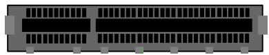
# 6.6. PCIe x4 Connector

PCIEA1: PCIe x4 Slot: Group 0 Lanes 0:3 assigned PCIe Slot

PCIEA2: PCIe x4 Slot: Group 0 Lanes 4:7 assigned PCIe Slot
![The image displays a horizontal, rectangular device, resembling a server chassis or storage array. It has a dark front panel featuring two large upper rectangular sections and a narrower lower section, all filled with vertical parallel lines suggesting ventilation slots or drive bays. A lighter grey vertical panel is located on the far left edge. Along the bottom edge, six small, light grey oval shapes are spaced evenly, representing feet. There is no text in the image.](.com-hpc-server-base-manual-50m-77106-1000-10-230720/54141b3131ed3addc10cdf1b3da13919b82f334c9105fa15a96eeba2caa35542.jpg)

<table><tr><td>Pin</td><td>Signal</td><td>Pin</td><td>Signal</td></tr><tr><td>B1</td><td>+12V</td><td>A1</td><td>PRSNT</td></tr><tr><td>B2</td><td>+12V</td><td>A2</td><td>+12V</td></tr><tr><td>B3</td><td>+12V</td><td>A3</td><td>+12V</td></tr><tr><td>B4</td><td>GND</td><td>A4</td><td>GND</td></tr><tr><td>B5</td><td>SMB_CLK</td><td>A5</td><td>JTAG</td></tr><tr><td>B6</td><td>SMB_DAT</td><td>A6</td><td>JTAG</td></tr><tr><td>B7</td><td>GND</td><td>A7</td><td>JTAG</td></tr><tr><td>B8</td><td>+3.3V</td><td>A8</td><td>JTAG</td></tr><tr><td>B9</td><td>JTAG</td><td>A9</td><td>+3.3V</td></tr><tr><td>B10</td><td>+3.3VAUX</td><td>A10</td><td>+3.3V</td></tr><tr><td>B11</td><td>WAKE</td><td>A11</td><td>PERST#</td></tr></table>

<table><tr><td>Pin</td><td>Signal</td><td>Pin</td><td>Signal</td></tr><tr><td>B12</td><td>RSVD</td><td>A12</td><td>GND</td></tr><tr><td>B13</td><td>GND</td><td>A13</td><td>REFCLK+</td></tr><tr><td>B14</td><td>PETp0</td><td>A14</td><td>REFCLK-</td></tr><tr><td>B15</td><td>PETn0</td><td>A15</td><td>GND</td></tr><tr><td>B16</td><td>GND</td><td>A16</td><td>PERp0</td></tr><tr><td>B17</td><td>PRSNT</td><td>A17</td><td>PERn0</td></tr><tr><td>B18</td><td>GND</td><td>A18</td><td>GND</td></tr><tr><td>B19</td><td>PETp1</td><td>A19</td><td>RSVD</td></tr><tr><td>B20</td><td>PETn1</td><td>A20</td><td>GND</td></tr><tr><td>B21</td><td>GND</td><td>A21</td><td>PERp1</td></tr><tr><td>B22</td><td>GND</td><td>A22</td><td>PERn1</td></tr></table>

<table><tr><td>Pin</td><td>Signal</td><td>Pin</td><td>Signal</td></tr><tr><td>B23</td><td>PETp2</td><td>A23</td><td>GND</td></tr><tr><td>B24</td><td>PETn2</td><td>A24</td><td>GND</td></tr><tr><td>B25</td><td>GND</td><td>A25</td><td>PERp2</td></tr><tr><td>B26</td><td>GND</td><td>A26</td><td>PERn2</td></tr><tr><td>B27</td><td>PETp3</td><td>A27</td><td>GND</td></tr><tr><td>B28</td><td>PETn3</td><td>A28</td><td>GND</td></tr><tr><td>B29</td><td>GND</td><td>A29</td><td>PERp3</td></tr><tr><td>B30</td><td>RSVD</td><td>A30</td><td>PERn3</td></tr><tr><td>B31</td><td>PRSNT</td><td>A31</td><td>GND</td></tr><tr><td>B32</td><td>GND</td><td>A32</td><td>RSVD</td></tr><tr><td></td><td></td><td></td><td></td></tr></table>

# 6.7. KEY-M Slot Connector

M2\_0: Group 0 Lanes 8-11 assigned M.2 Slot 1

M2\_1: Group 0 Lanes 12-15 assigned M.2 Slot 2
![The image displays a vertical, black rectangular label featuring the white text 'M.2' printed vertically along its length.](.com-hpc-server-base-manual-50m-77106-1000-10-230720/845abfa0e04f291626ef3148ff4f48afc0b5eb1e12a5376912d888b36678bb28.jpg)

<table><tr><td>Pin</td><td>Signal</td><td>Pin</td><td>Signal</td></tr><tr><td>1</td><td>CONFIG</td><td>2</td><td>+3.3V</td></tr><tr><td>3</td><td>GND</td><td>4</td><td>+3.3V</td></tr><tr><td>5</td><td>PERn3</td><td>6</td><td>N.C</td></tr><tr><td>7</td><td>PERp3</td><td>8</td><td>N.C</td></tr><tr><td>9</td><td>GND</td><td>10</td><td>DAS/DSS#</td></tr><tr><td>11</td><td>PETn3</td><td>12</td><td>+3.3V</td></tr><tr><td>13</td><td>PETp3</td><td>14</td><td>+3.3V</td></tr><tr><td>15</td><td>GND</td><td>16</td><td>+3.3V</td></tr><tr><td>17</td><td>PERn2</td><td>18</td><td>+3.3V</td></tr><tr><td>19</td><td>PERp2</td><td>20</td><td>N.C</td></tr><tr><td>21</td><td>CONFIG</td><td>22</td><td>N.C</td></tr><tr><td>23</td><td>PETn2</td><td>24</td><td>N.C</td></tr></table>

<table><tr><td>Pin</td><td>Signal</td><td>Pin</td><td>Signal</td></tr><tr><td>25</td><td>PETp2</td><td>26</td><td>N.C</td></tr><tr><td>27</td><td>GND</td><td>28</td><td>N.C</td></tr><tr><td>29</td><td>PERn1</td><td>30</td><td>N.C</td></tr><tr><td>31</td><td>PERp1</td><td>32</td><td>N.C</td></tr><tr><td>33</td><td>GND</td><td>34</td><td>N.C</td></tr><tr><td>35</td><td>PETn1</td><td>36</td><td>N.C</td></tr><tr><td>37</td><td>PETp1</td><td>38</td><td>DEVSLP</td></tr><tr><td>39</td><td>GND</td><td>40</td><td>N.C</td></tr><tr><td>41</td><td>PERn0</td><td>42</td><td>N.C</td></tr><tr><td>43</td><td>PERp0</td><td>44</td><td>N.C</td></tr><tr><td>45</td><td>GND</td><td>46</td><td>N.C</td></tr><tr><td>47</td><td>PETn0</td><td>48</td><td>N.C</td></tr></table>

<table><tr><td>Pin</td><td>Signal</td><td>Pin</td><td>Signal</td></tr><tr><td>49</td><td>PETp0</td><td>50</td><td>PETST#</td></tr><tr><td>51</td><td>GND</td><td>52</td><td>CLKREQ#</td></tr><tr><td>53</td><td>REFCLKN</td><td>54</td><td>PEWAKE#</td></tr><tr><td>55</td><td>REFCLKP</td><td>56</td><td>N.C</td></tr><tr><td>57</td><td>GND</td><td>58</td><td>N.C</td></tr><tr><td></td><td></td><td></td><td></td></tr><tr><td>67</td><td>N.C</td><td>68</td><td>SUSCLK</td></tr><tr><td>69</td><td>CONFIG</td><td>70</td><td>+3.3V</td></tr><tr><td>71</td><td>GND</td><td>72</td><td>+3.3V</td></tr><tr><td>73</td><td>GND</td><td>74</td><td>+3.3V</td></tr><tr><td>75</td><td>CONFIG</td><td></td><td></td></tr><tr><td></td><td></td><td></td><td></td></tr></table>

# 6.8. USB2.0 Ports Header

USB4\_5: USB2.0 Port 4 and Port 5 header

USB6\_7: USB2.0 Port 6 and Port 7 header

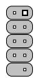
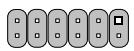
<table><tr><td>Pin</td><td>Signal</td><td></td><td></td></tr><tr><td>1</td><td>+5V</td><td>2</td><td>+5V</td></tr><tr><td>3</td><td>U2_USB_R_N</td><td>4</td><td>U2_USB_R_N</td></tr><tr><td>5</td><td>U2_USB_R_P</td><td>6</td><td>U2_USB_R_P</td></tr><tr><td>7</td><td>GND</td><td>8</td><td>GND</td></tr><tr><td>9</td><td>GND</td><td>10</td><td>NC</td></tr></table>

![A vertical column of six rounded rectangular shapes. The topmost shape contains a small square inside a square. The remaining five shapes each contain a small circle.](.com-hpc-server-base-manual-50m-77106-1000-10-230720/17f77624e0fcc354952cd3c63cd9dfff0c45202bcb304225ae7e9d6ddca76c6a.jpg)

# 6.9. USB3.x Ports Header

FP\_USB: USB Front Panel Header

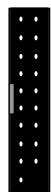
<table><tr><td>Pin</td><td>Signal</td><td></td><td></td></tr><tr><td>1</td><td>TP336</td><td>2</td><td>USB_DS3_DP_CN</td></tr><tr><td>3</td><td>USB2_P_CN</td><td>4</td><td>USB_DS3_DN_CN</td></tr><tr><td>5</td><td>USB2_N_CN</td><td>6</td><td>GND</td></tr><tr><td>7</td><td>GND</td><td>8</td><td>USB_SSTX5_P_CN</td></tr><tr><td>9</td><td>USB_SSTX4_P_CN</td><td>10</td><td>USB_SSTX5_N_CN</td></tr><tr><td>11</td><td>USB_SSTX4_N_CN</td><td>12</td><td>GND</td></tr><tr><td>13</td><td>GND</td><td>14</td><td>USB_SSRX5_P_CN</td></tr><tr><td>15</td><td>USB_SSRX4_P_CN</td><td>16</td><td>USB_SSRX5_N_CN</td></tr><tr><td>17</td><td>USB_SSRX4_N_CN</td><td>18</td><td>USB_VBUS</td></tr><tr><td>19</td><td>+5V</td><td></td><td></td></tr></table>

![The image displays a vertical black rectangular strip containing white circular dots arranged in columns. From left to right, the sequence consists of a single white dot, a vertical black separator, eight columns of two vertically aligned white dots, a vertical black separator, and two single vertically aligned white dots.](.com-hpc-server-base-manual-50m-77106-1000-10-230720/6368ebb7594bda05b3224bfe2213960e6a7099d480cbc2e36b975c8832000d76.jpg)

# 6.10. SATA Port

SATA0/SATA1: Serial ATA Port

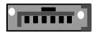
<table><tr><td>Pin</td><td>Signal</td></tr><tr><td>1</td><td>GND</td></tr><tr><td>2</td><td>TX_P</td></tr><tr><td>3</td><td>TX_N</td></tr><tr><td>4</td><td>GND</td></tr><tr><td>5</td><td>RX_P</td></tr><tr><td>6</td><td>RX_N</td></tr><tr><td>7</td><td>SATA0_P7</td></tr></table>

![The image shows a horizontal grey rectangular object with a black outline. Inside the object, there is a dark grey horizontal rectangle near the top center. Below that is a row of seven dark grey vertical rectangles. On the far left and far right sides, there are white circles.](.com-hpc-server-base-manual-50m-77106-1000-10-230720/7d3bfb4f77072a671eff8be83317ddd860ad5cb773f46d12b53f5a295cda779e.jpg)

JP\_S0/JP\_S1: Voltage supply switching for +3.3V or 5V for SATA DOM.

<table><tr><td>Pin</td><td>Status</td></tr><tr><td>1-2</td><td>+3.3V for SATA</td></tr><tr><td>2-3</td><td>+5V for SATA</td></tr><tr><td>NC</td><td>Default</td></tr></table>

![The image displays a vertical column of numbers on the left: '1', '2', and '3'. To the right of each number is a grey circle. Inside the top circle (aligned with '1') is a black square. Inside the middle circle (aligned with '2') is a white square. Inside the bottom circle (aligned with '3') is a white square.](.com-hpc-server-base-manual-50m-77106-1000-10-230720/34dd8edf2b3237dbda7f73d4a296f1054deccbfc31e59e910833436519789d2d.jpg)

# 6.11. eSPI Debug Connector

ESPI: for eSPI debugging connection purpose

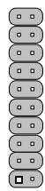
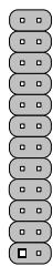
<table><tr><td>Pin</td><td>Signal</td><td>Pin</td><td>Signal</td></tr><tr><td>1</td><td>eSPI_CLK</td><td>2</td><td>GND</td></tr><tr><td>3</td><td>eSPI_CS0</td><td>4</td><td>eSPI_RST</td></tr><tr><td>5</td><td>RST_DBG_L</td><td>6</td><td>+5V</td></tr><tr><td>7</td><td>eSPI_IO_3</td><td>8</td><td>eSPI_IO_1</td></tr><tr><td>9</td><td>+ 3.3VSB</td><td>10</td><td>eSPI_IO_1</td></tr><tr><td>11</td><td>eSPI_IO_0</td><td>12</td><td>GND</td></tr><tr><td>13</td><td>SMB_CK</td><td>14</td><td>CN_SNB_DAT</td></tr><tr><td>15</td><td>BIOSRST</td><td>16</td><td>NC</td></tr><tr><td>17</td><td>GND</td><td>18</td><td>eSPI_CS1#</td></tr><tr><td>19</td><td>eSPI_ALEART0#</td><td>20</td><td>eSPI_ALEART1#</td></tr></table>

![This image displays a vertical column of twelve identical remote control buttons. Each button is a light gray, rounded rectangle (pill shape) with a black outline. Inside each button is a black icon consisting of a square centered within a larger square outline. The buttons are stacked vertically with small gaps between them against a plain, light background.](.com-hpc-server-base-manual-50m-77106-1000-10-230720/d46f7c36d38644206f73c2c0a374c1a5de1b09a5087d546ea3283cab6f13f5df.jpg)

# 6.12. BMC Debug Connector

BMC\_DBG: UART5 for BMC firmware debugging

<table><tr><td>Pin</td><td>Signal</td></tr><tr><td>1</td><td>UART_DBG_TXD5</td></tr><tr><td>2</td><td>GND</td></tr><tr><td>3</td><td>UART_DBG_RXD5</td></tr></table>

![The image displays a vertical column of three identical light-grey, rounded rectangular shapes against a black background. Inside each grey shape is a centered white square with a black border, and within that white square is a smaller, solid black square.](.com-hpc-server-base-manual-50m-77106-1000-10-230720/db6aee1bd06e4294ae0bf81ea1c4a5164440a4d44367183d6a462e65c11c8ae2.jpg)

# 6.13. COM Port Connector

COM1: the Module UART port1

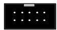
<table><tr><td>Pin</td><td>Signal</td><td></td><td></td></tr><tr><td>1</td><td>CM1_DCD</td><td>2</td><td>CN1_DSR</td></tr><tr><td>3</td><td>SER1_RX</td><td>4</td><td>SER1_RTS_L</td></tr><tr><td>5</td><td>SER1_TX</td><td>6</td><td>SER1_CTS_L</td></tr><tr><td>7</td><td>CM1_DTR</td><td>8</td><td>CM1_RI</td></tr><tr><td>9</td><td>GND</td><td>10</td><td>NC</td></tr></table>

![The image displays a black rectangle with rounded corners set against a white background. Inside the black rectangle, there is a white pill-shaped outline at the top center. Below this outline, twelve white dots are arranged in a grid of three rows and four columns.](.com-hpc-server-base-manual-50m-77106-1000-10-230720/fcac0742ed3d87ea225e9898f0eb1eeb38ca7fbaf07f26497fb6103ec5163055.jpg)

JP9: MUX of Module UART1 or BMC UART SOL

<table><tr><td>Jumper</td><td>Status</td></tr><tr><td>1-2</td><td>BMC UART2 SOL &lt;&lt;&lt;</td></tr><tr><td>2-3</td><td>Module’s UART1</td></tr></table>

![The image features a vertical column of black numbers '1', '2', and '3' on the left side. To the right is a grey rectangular outline containing three vertically stacked circles. The top circle contains a single black square in its center. The middle circle contains four small white squares arranged in a square pattern. The bottom circle is empty.](.com-hpc-server-base-manual-50m-77106-1000-10-230720/bb9ad5bc1ac06d65ee0a74c009536519b4e35135c9994c813eda22127c3ce60e.jpg)

JP34: MUX of Module UART0 or BMC UART1 (Console)

<table><tr><td>Jumper</td><td>Status</td></tr><tr><td>1-2</td><td>BMC UART1 Console</td></tr><tr><td>2-3</td><td>Module UART0 &lt;&lt;&lt;</td></tr></table>

![The image displays a vertical column of numbers on the left reading 1, 2, and 3. To the right is a corresponding column of three gray circles. The top circle features a black square with a white center. The bottom two circles are enclosed within a thin rectangular outline and each contains a white square with a black center.](.com-hpc-server-base-manual-50m-77106-1000-10-230720/a6b2bed5bae694e608d0ee31ade870eeaace75f9988a109dcf7c6a7a052d0e3c.jpg)

# 6.14. I2C0/1 and SMBus Header

CN23: Module outputs I2C0/1 and SMBus external header

<table><tr><td>Pin</td><td>Signal</td><td>Pin</td><td>Signal</td></tr><tr><td>1</td><td>+3.3V</td><td>2</td><td>+3.3V</td></tr><tr><td>3</td><td>SMB_CLK</td><td>4</td><td>I2C0_CLK</td></tr><tr><td>5</td><td>SMB_DAT</td><td>6</td><td>I2C0_DAT</td></tr><tr><td>7</td><td>+3.3V</td><td>8</td><td>I2C0_ALERT-L</td></tr><tr><td>9</td><td>I2C1_CLK</td><td>10</td><td>GND</td></tr><tr><td>11</td><td>I2C1_DAT</td><td>12</td><td>GND</td></tr></table>

![A horizontal row of six grey, rectangular light switch plates arranged against a white background. Each plate is labeled with a small number near the top, reading sequentially from 1 to 6 from left to right.\n\nFrom left to right:\n- The first switch (1) is toggled up (ON) with a white rectangular toggle.\n- The second switch (2) is toggled down (OFF) with a white rectangular toggle.\n- The third switch (3) is toggled up (ON) with a white rectangular toggle.\n- The fourth switch (4) is toggled down (OFF) with a white rectangular toggle.\n- The fifth switch (5) is toggled up (ON) with a white rectangular toggle.\n- The sixth switch (6) is toggled down (OFF) but features a black square toggle, distinct from the white toggles on the other switches.](.com-hpc-server-base-manual-50m-77106-1000-10-230720/3e368aad456464e8bc078adcb1c4247eae37676d9479f3f14793eede39386214.jpg)

# 6.15. GPIO Header

CN24: Module outputs GPIO Header

<table><tr><td>Pin</td><td>Signal</td><td>Pin</td><td>Signal</td></tr><tr><td>1</td><td>+3.3V</td><td>2</td><td>GPIO_06</td></tr><tr><td>3</td><td>GPIO_00</td><td>4</td><td>GPIO_07</td></tr><tr><td>5</td><td>GPIO_01</td><td>6</td><td>GPIO_08</td></tr><tr><td>7</td><td>GPIO_02</td><td>8</td><td>GPIO_09</td></tr><tr><td>9</td><td>GPIO_03</td><td>10</td><td>GPIO_10</td></tr><tr><td>11</td><td>GPIO_04</td><td>12</td><td>GPIO_11</td></tr><tr><td>13</td><td>GPIO_05</td><td>14</td><td>GND</td></tr></table>

![The image displays a horizontal row of eight identical grey, capsule-shaped objects against a white background. Each capsule has a thick black outline and features three small black squares arranged in a vertical column in the center. There is no text in the image.](.com-hpc-server-base-manual-50m-77106-1000-10-230720/452ab68eb8898b05da9b56e0c48fd248149fcb13dd6ba9796a20a4922e09efec.jpg)

# 6.16. External SMBus Header

CN35: External SMBus for connecting to the MUX of KR/SFI

<table><tr><td>Pin</td><td>Signal</td></tr><tr><td>1</td><td>GND</td></tr><tr><td>2</td><td>N.C</td></tr><tr><td>3</td><td>RT_SDC</td></tr><tr><td>4</td><td>RT_SDA</td></tr></table>

![The image displays four identical grey circles arranged horizontally in a row. Each circle has a black border and contains a smaller, lighter grey square in its center. There is no text present in the image.](.com-hpc-server-base-manual-50m-77106-1000-10-230720/d112b55f6ce5c4b1388737cda873276fa142f85c8c11e06df921386674e1212a.jpg)

# 6.17. Fan Header

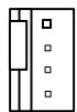
FAN\_0: Module controlled FAN

<table><tr><td>Pin</td><td>Signal</td></tr><tr><td>1</td><td>GND</td></tr><tr><td>2</td><td>+12V_5V_FAN</td></tr><tr><td>3</td><td>SENSE_FAN</td></tr><tr><td>4</td><td>PWMOUT_FAN</td></tr></table>

![The image displays a simple black-and-white line drawing of a refrigerator. On the left side, there is a door featuring a vertical handle. On the right side, a control panel is depicted, consisting of a square at the top followed by four smaller squares arranged vertically below it.](.com-hpc-server-base-manual-50m-77106-1000-10-230720/a21b8de1db11523ce5e28e91b41fd834eaa183313a90c4177a3319113db54622.jpg)

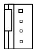
FAN\_1: BMC controlled FAN 1

<table><tr><td>Pin</td><td>Signal</td></tr><tr><td>1</td><td>GND</td></tr><tr><td>2</td><td>+12V_5V_FAN0</td></tr><tr><td>3</td><td>SENSE_FAN0</td></tr><tr><td>4</td><td>PWMOUT_FAN0</td></tr></table>

![The image displays a simple black and white line drawing resembling a schematic or block diagram. On the left side, two narrow vertical rectangles are positioned side-by-side. To their right, a larger section contains a vertical column of four squares. The top square features a small black square in its center, while the three squares beneath it are empty outlines. There is no text present in the image.](.com-hpc-server-base-manual-50m-77106-1000-10-230720/7131c324eef826c85d7cabe35e2ada1764c6b4c08876293e59af99a96c78bad5.jpg)

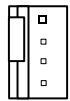
FAN\_2: BMC controlled FAN 2

<table><tr><td>Pin</td><td>Signal</td></tr><tr><td>1</td><td>GND</td></tr><tr><td>2</td><td>+12V_5V_FAN1</td></tr><tr><td>3</td><td>SENSE_FAN1</td></tr><tr><td>4</td><td>PWMOUT_FAN1</td></tr></table>

![This is a black-and-white line drawing depicting a schematic of a door. On the left side, a vertical rectangular frame is shown, containing a horizontal rectangle near the top and a long vertical rectangle below it. To the right is the main door panel, which features a vertical column of four small squares aligned near its left edge; the top square is filled in solid black, while the three squares below it are white outlines.](.com-hpc-server-base-manual-50m-77106-1000-10-230720/205ba8faa2ab96f033481d808895ca04d4512b9fecf1502bda601f98836cac17.jpg)

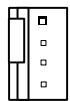
FAN\_4: BMC controlled FAN 4

<table><tr><td>Pin</td><td>Signal</td></tr><tr><td>1</td><td>GND</td></tr><tr><td>2</td><td>+12V_5V_FAN3</td></tr><tr><td>3</td><td>SENSE_FAN3</td></tr><tr><td>4</td><td>PWMOUT_FAN3</td></tr></table>

![The image is a black and white line drawing of a vertical rectangle. On the left side, there is a vertical assembly consisting of a small square at the top and long rectangular shapes below it. On the right side, there is a large area containing a vertical column of four small squares.](.com-hpc-server-base-manual-50m-77106-1000-10-230720/06d69adabed69b0fef1c2682dde2f25edf111d70ed2fc5d54ffb3da490bc6ec1.jpg)

FAN\_5: BMC controlled FAN 5

<table><tr><td>Pin</td><td>Signal</td></tr><tr><td>1</td><td>GND</td></tr><tr><td>2</td><td>+12V_5V_FAN4</td></tr><tr><td>3</td><td>SENSE_FAN4</td></tr><tr><td>4</td><td>PWMOUT_FAN4</td></tr></table>

![The image is a black and white line drawing depicting a vertical rectangular object divided into two main sections.\n\nOn the left side, there is a narrower vertical column containing three rectangular compartments stacked vertically: a small top rectangle, a larger middle rectangle, and a small bottom rectangle.\n\nOn the right side, there is a wider vertical column containing four small squares arranged in a vertical stack. The top square is filled solid black. The three squares below it are outlined and each contains a smaller solid black square in its center.](.com-hpc-server-base-manual-50m-77106-1000-10-230720/7fbcc5d9f94b5554f67dde69b3be2bc4a67058560c2ef5415cceb913c8eff6bd.jpg)

# 6.18. General Purpose SPI Header

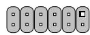
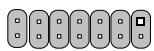
GP\_SPI: General Purpose SPI connector for widely used interfaces

<table><tr><td>Pin</td><td>Signal</td><td>Pin</td><td>Signal</td></tr><tr><td>1</td><td>+3.3V</td><td>2</td><td>NC</td></tr><tr><td>3</td><td>GP_SPI_CLK</td><td>4</td><td>GP_SPI_MOSI</td></tr><tr><td>5</td><td>GP_SPI_CS2</td><td>6</td><td>GP_SPI_MISO</td></tr><tr><td>7</td><td>GP_SPI_CS3</td><td>8</td><td>GP_SPI_CS0</td></tr><tr><td>9</td><td>GP_SPI_ALT</td><td>10</td><td>GP_SPI_CS1</td></tr><tr><td>11</td><td>NC</td><td>12</td><td>GND</td></tr></table>

![The image displays a horizontal row of eight rounded rectangular shapes. The first seven shapes from the left are identical, featuring a grey border, a light grey interior, and three small white circles arranged vertically within each. The eighth shape on the far right has a black border. Inside this final shape, the top element is a black-outlined square, while the middle and bottom elements are small white circles.](.com-hpc-server-base-manual-50m-77106-1000-10-230720/2c28211b014577d0350681a3a605794ec325b2b78fbc6a7a4f30b4f0c2a0876d.jpg)

# 6.19. IPMI Header

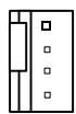
IPMI: Intelligent Platform Management Bus for platform management functions

<table><tr><td>Pin</td><td>Signal</td></tr><tr><td>1</td><td>+3.3V</td></tr><tr><td>2</td><td>IPMB_DAT</td></tr><tr><td>3</td><td>IPMB_CLK</td></tr><tr><td>4</td><td>GND</td></tr></table>

![The image displays four grey circles with black outlines arranged in a horizontal row against a white background. Each circle contains a small black square in its center. A thin black line runs across the top edge of the image.](.com-hpc-server-base-manual-50m-77106-1000-10-230720/fb53ba9ce8ec82c2a1850f2e254567c8f354b400f8bbca62316616317bc4eefb.jpg)

# 6.20. Front Panel Control

FRONT\_PANEL: Power Button, Reset Button, HDD LED, Power LED for front panel header

<table><tr><td>Pin</td><td>Signal</td><td>Pin</td><td>Signal</td></tr><tr><td>23</td><td>LAN2_LED_N</td><td>24</td><td>NMI_SW</td></tr><tr><td>21</td><td>LAN2_LED_P</td><td>22</td><td>GND</td></tr><tr><td>19</td><td>CASE_OPEN_N</td><td>20</td><td>R_UID_BUT_P</td></tr><tr><td>17</td><td>SENSOR_SCL</td><td>18</td><td>GND</td></tr><tr><td>15</td><td>SENSOR_SDA</td><td>16</td><td>RST_BUT_P</td></tr><tr><td>13</td><td>LAN1_LED_N</td><td>14</td><td>GND</td></tr><tr><td>11</td><td>LAN1_LED_P</td><td>12</td><td>PWR_BUT_P</td></tr><tr><td>9</td><td>SLED_R</td><td>10</td><td>HDD_LED_N</td></tr><tr><td>7</td><td>SLED_G</td><td>8</td><td>HDD_LED_P</td></tr><tr><td>5</td><td>UID_LED_P</td><td>6</td><td>PWR_LED_N</td></tr><tr><td>3</td><td>UID_LED_N</td><td>4</td><td>FAN_FAIL_LED_N</td></tr><tr><td>1</td><td>5VSB</td><td>2</td><td>PWR_LED_P</td></tr></table>

![A vertical column of ten grey buttons with rounded corners. Each button contains a small square on the left and a small circle on the right. The top nine buttons display white squares and white circles, while the bottom button displays a black square and a white circle.](.com-hpc-server-base-manual-50m-77106-1000-10-230720/769e701e9299365acc13d7eeeeea55ff34ac87113933d85203b04b3059972d00.jpg)

# 6.21. Power Connectors

# ATX\_24: ATX 24-pin Power Connector

Connect the ATX 24-pin (or 20-pin) connector to supply power to COM-HPC Server Base carrier.

<table><tr><td>Pin</td><td>Signal</td><td>Pin</td><td>Signal</td></tr><tr><td>1</td><td>+3.3V</td><td>13</td><td>+3.3V</td></tr><tr><td>2</td><td>+3.3V</td><td>14</td><td>-12V</td></tr><tr><td>3</td><td>GND</td><td>15</td><td>COM</td></tr><tr><td>4</td><td>+5V</td><td>16</td><td>PWR_ON</td></tr><tr><td>5</td><td>GND</td><td>17</td><td>COM</td></tr><tr><td>6</td><td>+5V</td><td>18</td><td>COM</td></tr><tr><td>7</td><td>GND</td><td>19</td><td>COM</td></tr><tr><td>8</td><td>PWR_GOOD</td><td>20</td><td>-5V</td></tr><tr><td>9</td><td>+5VSB</td><td>21</td><td>+5V</td></tr><tr><td>10</td><td>+12V</td><td>22</td><td>+5V</td></tr><tr><td>11</td><td>+12V</td><td>23</td><td>+5V</td></tr><tr><td>12</td><td>+3.3V</td><td>24</td><td>COM</td></tr></table>

![Simple line drawing of a vertical door with multiple compartments and a handle (no text or symbols)](.com-hpc-server-base-manual-50m-77106-1000-10-230720/54c2d0110f1080dbde319950247147d42ddda47a080b557f95a05ade666ce53b.jpg)

# ATX\_8: ATX 12V 8-pin Connector.

Connect the ATX 12V 8-pin connector

to supply power to the COM-HPC Server module.

<table><tr><td>Pin</td><td>Signal</td></tr><tr><td>1</td><td>GND</td></tr><tr><td>2</td><td>GND</td></tr><tr><td>3</td><td>GND</td></tr><tr><td>4</td><td>GND</td></tr><tr><td>5</td><td>+12V</td></tr><tr><td>6</td><td>+12V</td></tr><tr><td>7</td><td>+12V</td></tr><tr><td>8</td><td>+12V</td></tr></table>

![The image is a black and white line drawing of a floor plan. It depicts a large rectangle divided into a grid of 12 smaller rectangular rooms arranged in three columns and four rows.\n\nInside each room is a semi-circle shape, likely representing a bed. The orientation of these shapes varies by column:\n*   **Left Column:** The semi-circles in all four rooms have their flat sides against the right wall (curved side facing left).\n*   **Middle Column:** The semi-circles in all four rooms have their flat sides against the left wall (curved side facing right).\n*   **Right Column:** The semi-circles in the top, second, and bottom rooms have their flat sides against the left wall. However, the room in the third row from the top is different: its semi-circle has its flat side against the right wall. Additionally, this specific room features a small rectangular door on its left wall that opens into the adjacent room in the middle column.](.com-hpc-server-base-manual-50m-77106-1000-10-230720/d2b0b02ea706bd7818f8b340d2bf2da6716d06e824965ac1aed2585c58cae050.jpg)

# 6.22. Carrier EEPROM Address Switch

SW1: COM-HPC Carrier Board EEPROM address setting

Default Address: AEh

<table><tr><td>1</td><td>0</td><td>1</td><td>0</td><td>A2</td><td>A1</td><td>A0</td><td>R/W</td></tr><tr><td colspan="8">MSB LSB</td></tr></table>

<table><tr><td>SW1</td><td>I2C EEPROM_U53</td></tr><tr><td>1-8</td><td>A2_OFF</td></tr><tr><td>2-7</td><td>A1_OFF</td></tr><tr><td>3-6</td><td>A0_OFF</td></tr></table>

![The image displays a black rectangular panel featuring four white slide switches arranged in a horizontal row. Above the switches, the text 'ON DIP' is printed in white capital letters. Below the switches, the numbers '1 2 3 4' are printed in white, corresponding to each switch from left to right. All four switches are currently in the upward position.](.com-hpc-server-base-manual-50m-77106-1000-10-230720/fecf917642c727f0ccf1f31f128d4b8bc402d3583daf393ae74837bf0a6b4f17.jpg)

# 6.23. Module (I2C0) / BMC (I2C8) Jumpers

JP2: I2C CLK switch for I2C8 (BMC) or I2C0 (module)

<table><tr><td>Jumper</td><td>Status</td></tr><tr><td>1-2</td><td>I2C8, BMC</td></tr><tr><td>2-3</td><td>I2C0, Module</td></tr></table>

![The image displays the numbers 1, 2, and 3 arranged vertically on the left side. To the right of these numbers is a rectangular outline containing three grey circles stacked vertically. The top circle, aligned with the number 1, contains a small black square in its center. The middle circle, aligned with the number 2, also contains a small black square. The bottom circle, aligned with the number 3, is a solid grey circle without an inner shape.](.com-hpc-server-base-manual-50m-77106-1000-10-230720/e68ac91e5e63f3704d7fa68484f4d736258958cfcccd8b01c5e34eb75a3ed816.jpg)

JP3: I2C DAT switch for I2C8 (BMC) or I2C0 (module)

<table><tr><td>Jumper</td><td>Status</td></tr><tr><td>1-2</td><td>I2C8, BMC</td></tr><tr><td>2-3</td><td>I2C0, Module</td></tr></table>

![The image shows three rows. On the left, the numbers 1, 2, and 3 are listed vertically in black. On the right, corresponding to each number, is a vertical column of three grey circles. Inside the top circle is a small black square. Inside the middle circle is a small white square. Inside the bottom circle is a small grey square.](.com-hpc-server-base-manual-50m-77106-1000-10-230720/f3e5f4562ecd42cc393511d1c6b15fd17d45e3d4a0629e946510ef8b8918ba9d.jpg)

# 6.24. Other Jumpers

JP27/28/29: BIOS Selection.

Boot from SPI Secondary BIOS, see below for details.

Setting Boot from Module BIOS

<table><tr><td>JP29</td><td>JP28</td><td>JP27</td><td>BOOT</td></tr><tr><td>1-2</td><td>1-2</td><td>1-2</td><td>Module BIOS &lt;&lt;&lt;</td></tr></table>

![The image displays three vertical columns of black text and graphics on a white background. From left to right, the text reads 'JP29', 'JP28', and 'JP27'. The text is oriented vertically, reading downwards in each column. Below each text label is a graphic consisting of a square outline containing two vertically stacked grey circles. Inside each circle is a small white square with a black border.](.com-hpc-server-base-manual-50m-77106-1000-10-230720/7e8fc7984a1b92c039d48b817c74bdb61581455c01da79304d3e6636c912299f.jpg)

Setting Boot from Carrier BIOS

<table><tr><td>JP29</td><td>JP28</td><td>JP27</td><td>BOOT</td></tr><tr><td>1-2</td><td>1-2</td><td>2-3</td><td>Carrier BIOS &lt;&lt;&lt;&lt;</td></tr></table>

![The image displays three vertical columns of black text and diagrams on a white background. From left to right, the text labels are arranged vertically, reading 'JP29', 'JP28', and 'JP27'. Below each label is a square outline. Inside each square are three grey circles, each containing a small white square in its center. The circles are positioned in the top-left, bottom-left, and bottom-right corners, leaving the top-right corner empty. The diagrams appear identical in all three columns.](.com-hpc-server-base-manual-50m-77106-1000-10-230720/229aca7929f5087ba6119c6d84c4e877d439886e72ffb573c0494145f98b6ab5.jpg)

JP30: Clear CMOS

To clear CMOS, shut down the power and short pins 2 and 3 (short VBT to ground)

<table><tr><td>Jumper</td><td>Status</td></tr><tr><td>1-2</td><td>Normal &lt;&lt;&lt;</td></tr><tr><td>2-3</td><td>Clear CMOS</td></tr></table>

![The image displays a vertical list of numbers 1, 2, and 3. To the right of these numbers is a column of three gray circles enclosed within a thin rectangular border. Inside the top circle is a small black square. Inside the middle and bottom circles are small white squares.](.com-hpc-server-base-manual-50m-77106-1000-10-230720/2b07da5fcd3c369ead3d5d39dd60f825bcf4c1fc9b2252cfbc4c3bfa7f8de11b.jpg)

# 6.25. Power Jumpers

JP31: AT/ATX Mode

In AT mode, put PS\_ON# to ground as short pin 2-3 to force power on.

<table><tr><td>Jumper</td><td>Status</td></tr><tr><td>1-2</td><td>ATX Mode</td></tr><tr><td>2-3</td><td>AT Mode &lt;&lt;&lt;&lt;</td></tr></table>

![The image shows a vertical list with two columns. On the left are the numbers **1**, **2**, and **3** stacked vertically in black text. On the right are three grey circular buttons stacked vertically, aligned with the numbers. The top button, next to the number 1, features a large, solid black square in its center. The middle button, next to the number 2, features a small square in its center. The bottom button, next to the number 3, features a small square in its center.](.com-hpc-server-base-manual-50m-77106-1000-10-230720/f1cb66e219c390976d016e24d16ed0be7bf5e882bce666d629b0dfaa6e87dbe8.jpg)

# JP32: ATX S3 signal switching

In AT mode, put pin 2-3 for S5 output instead Power Button (S3)

<table><tr><td>Jumper</td><td>Status</td></tr><tr><td>1-2</td><td>ATX (SUS_S3#) &lt; &lt; &lt; &lt;</td></tr><tr><td>2-3</td><td>AT (SUS_S5#)</td></tr></table>

![The image displays a vertical list of numbers on the left side: 1, 2, and 3. To the right of these numbers is a column of three grey circles, all enclosed within a thin black rectangular border. The top circle, aligned with the number 1, contains a small black square in its center. The middle and bottom circles, aligned with numbers 2 and 3 respectively, are plain grey without any central markings.](.com-hpc-server-base-manual-50m-77106-1000-10-230720/bf23dbb56d338ca7bf53ed0f3bf748e69db5eebe2131b9f1dcdb7046f225c950.jpg)

JP33: VCC\_12V On/Off during S3/S5

In AT mode, put pin 2-3 to output 12V during S3/S5.

<table><tr><td>Jumper</td><td>Status</td></tr><tr><td>1-2</td><td>ATX Mode</td></tr><tr><td>2-3</td><td>AT Mode &lt;&lt;&lt;</td></tr></table>

![The image displays a vertical list with numbers on the left and icons on the right. On the left, the numbers '1', '2', and '3' are stacked vertically in black text. On the right, there are three rounded rectangular buttons stacked vertically. Next to '1', there is a grey circle containing a black square with a small white dot in the center. Next to '2' and '3', there are grey circles containing concentric circles (grey, black, white, grey, black) and a white dot in the center.](.com-hpc-server-base-manual-50m-77106-1000-10-230720/22546b98f9e99cf7717d026f1ca8c265767f2a948fb952c84f88099a8bbf6fcf.jpg)

JP35: +5V\_SBY supply

In AT mode, put pin 3-4 to output +5V\_SBY directly.

<table><tr><td>Jumper</td><td>Status</td></tr><tr><td>2-3</td><td>ATX PSU &lt;&lt;&lt;</td></tr><tr><td>3-4</td><td>AT (DC to DC)</td></tr></table>

![A vertical column of the numbers 1, 2, 3, and 4 is on the left side. To the right of each number is a gray circle. The top circle contains a small black square.](.com-hpc-server-base-manual-50m-77106-1000-10-230720/a2b53cf746f0cfe08febdc99a539dbe97f40cdf1a3bfc1521bb3c1015da014d0.jpg)

# 7. Secondary BIOS

The COM-HPC Server-Base supports Secondary BIOS, using Boot Serial Peripheral Interface (SPI) for COM-HPC modules.

Secondary BIOS solutions can be used as an alternative to the on-module BIOS and provide support for the following:

• Testing new BIOS versions
• Development of firmware modifications
• Recovery if soldered BIOS on module is corrupted

To use the BIOS on the module;

short pins 1-2 on JP27, JP28, JP29, reference section 6.23

To use the BIOS on the carrier board;

Short pins 2-3 on JP27, and keep pin 1-2 on JP28, JP29, reference section 6.23

Make sure that the secondary BIOS flash chip has been properly installed into the Carrier BIOS socket before BOOT BIOS adjusting.
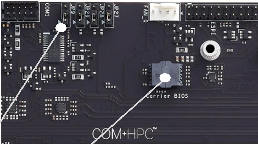
![COM1\nJP9\nJP29\nJP28\nJP27\nFAN_0\nESPI\nCarrier BIOS\nCOM+HPC™](.com-hpc-server-base-manual-50m-77106-1000-10-230720/a64660d6626eb75c0ecb814ad3af1ec50dec780c20897e65efc733a4ab44c803.jpg)

# 8. Switches, POST and LEDs

# 8.1. Switches (S0-S5)

There are two switches, at the center and lower-right of the carrier.

# PWR\_BTN

Indicates getting into S0 from S5 of the system.
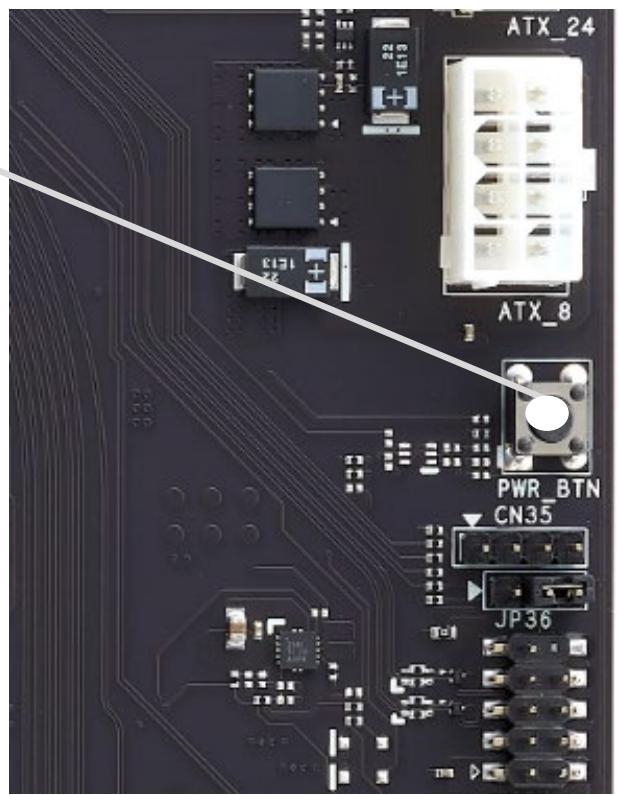
![ATX_24\nATX_8\nPWR_BTN\nCN35\nJP36](.com-hpc-server-base-manual-50m-77106-1000-10-230720/5bf6f614da351845be1cd65e85af68cfd19f5bae102a621c25e9f2efa9332259.jpg)

# RST\_BTN

Indicates resetting of the system.
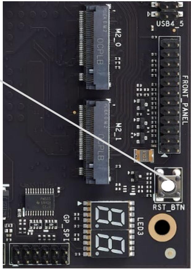
![USB4_5\nFRONT PANEL\nM2-0\nM2-1\nRST_BTN\nLED3\nGP_SP1](.com-hpc-server-base-manual-50m-77106-1000-10-230720/b7afb9863c4885a07fc569b15b12756f063d601eade7f453d0678439fcffd022.jpg)

# 8.2. POST and inductors LEDs

An eSPI-based POST display is added for debugging.

The two 7-SEG LEDs shows the actual POST data.
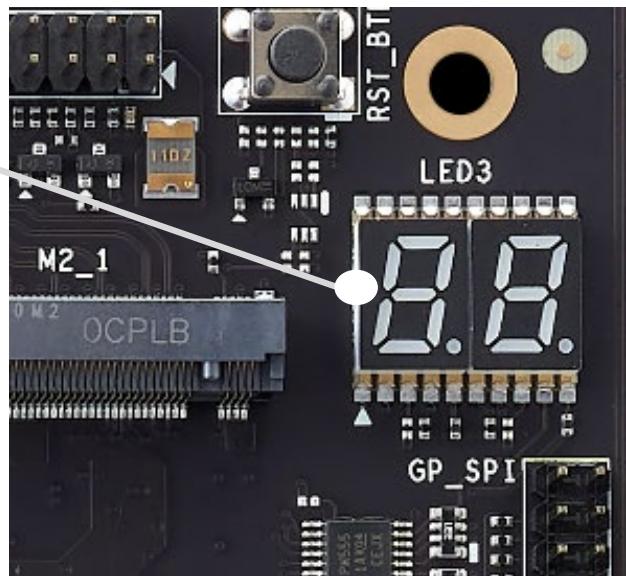
![M2_1\n0 M2 OCPLB\nRST_BT\nLED3\n8.8.\nGP_SPI](.com-hpc-server-base-manual-50m-77106-1000-10-230720/fc9e0f0f1ff2a834d353975161c8fe16fcbd25d3e724273d8cc5f587efafb10b.jpg)

A row of mini-LEDs below the POST display indicates the following:

5VSB: ATX power attached on standby or active

S3: Indicates S3 status

PWR\_ON: Indicates power on

WDT: Indicates WDT (watchdog timer) activity

BMC\_HB: Heart beat LED indicator output
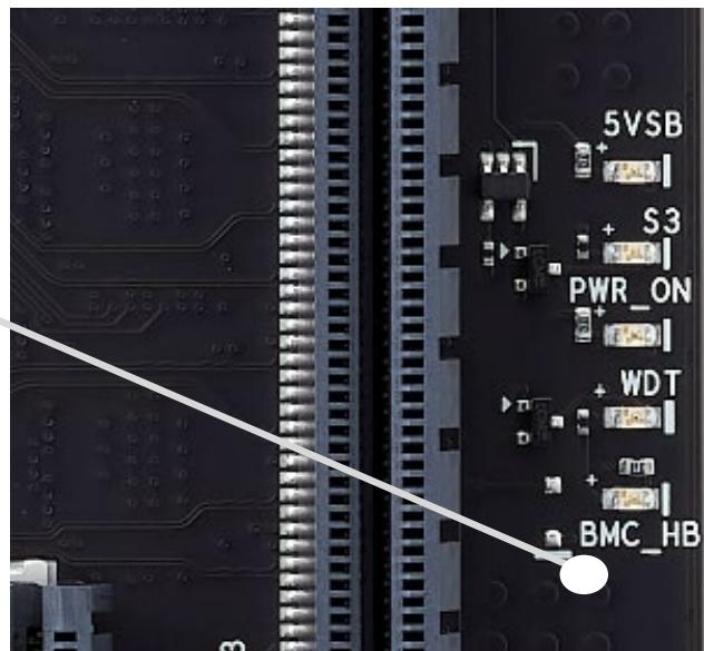
![5VSB\nS3\nPWR_ON\nWDT\nBMC_HB](.com-hpc-server-base-manual-50m-77106-1000-10-230720/14c2a054c2d36443677b0306e2dd9701da7731e6fd832312408796e64f1f9fd8.jpg)

# 8.3. ATX Power Connectors

The COM-HPC Server Base has one ATX 24-pin connector to supply power to the carrier board and one ATX 12V 8-pin connector to supply power to the COM-HPC module.

The system will not power on unless an ATX 12V 8-pin connector is connected.

If your power supply has a 24-pin ATX connector, then attach the connectors as shown.
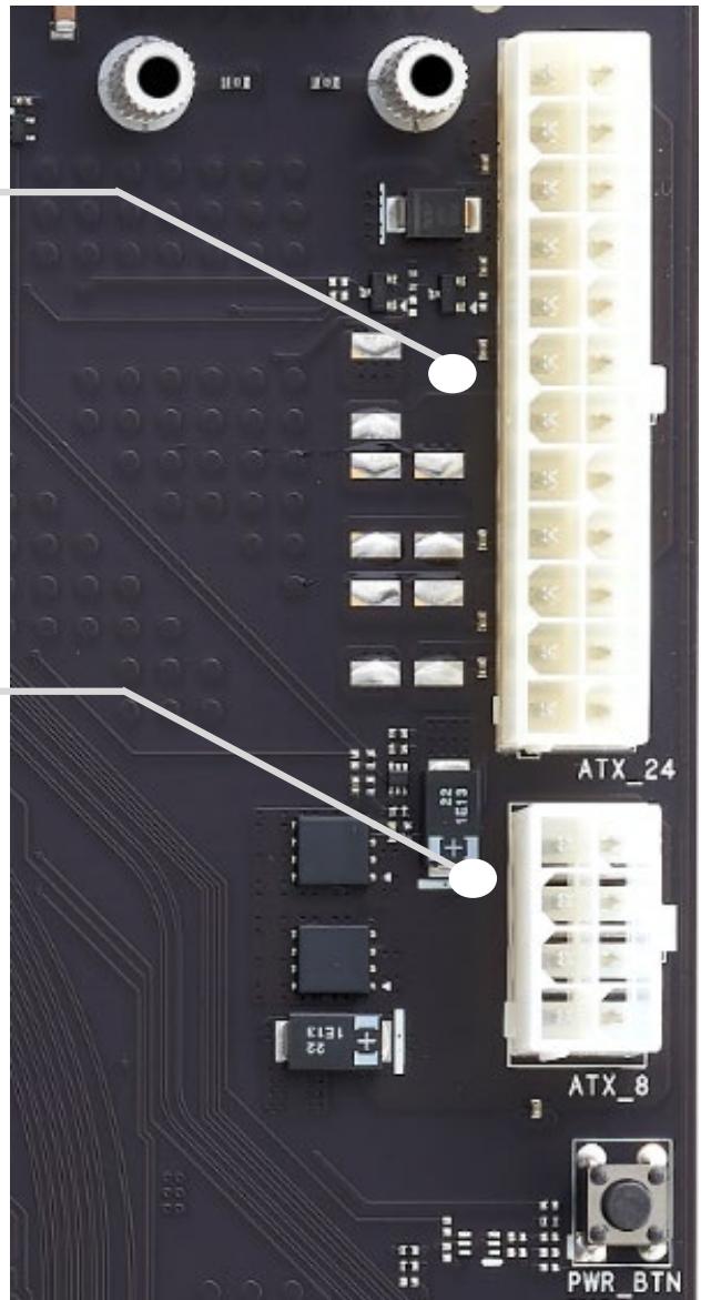
![ATX_24\nATX_8\nPWR_BTN](.com-hpc-server-base-manual-50m-77106-1000-10-230720/a0778dfea78c3a0d566abdcb72803e4158ea1f2ac19928fc1f8aa9a2edf06b27.jpg)

# 8.4. AT Power Mode

To operate the system in AT Mode with an ATX power supply,

Refer to section 6.24 jumper settings for details, or follow the instruction below.

Jumper Settings for ATX mode

<table><tr><td>JP31</td><td>JP32</td><td>JP33</td><td>JP35</td><td>POWER MODE</td></tr><tr><td>1-2</td><td>1-2</td><td>1-2</td><td>2-3</td><td>ATX Mode</td></tr></table>

![JP33 JP32 JP31\nJP35](.com-hpc-server-base-manual-50m-77106-1000-10-230720/14fee646e381ca450492dfbaee91218bf2454d287c73b2ab373588d3c495228d.jpg)

Jumper Settings for AT mode

<table><tr><td>JP31</td><td>JP32</td><td>JP33</td><td>JP35</td><td>POWER MODE</td></tr><tr><td>2-3</td><td>2-3</td><td>2-3</td><td>3-4</td><td>AT Mode</td></tr></table>

![JP33 JP32 JP31\nJP35](.com-hpc-server-base-manual-50m-77106-1000-10-230720/4719751eb59af6966aabc983085a60b956c0ed5200567344ea23fbc51e2b232e.jpg)

![S\nIPMI\nJP33 JP32 JP31\nJP35\nJP3\nJP2\nBMC_DBG](.com-hpc-server-base-manual-50m-77106-1000-10-230720/cc51efb78d0e36a469f38441bde22aa0afeab99bfdae43618f5e20f708f0dc65.jpg)
[🔗 Link to the original document](.com-hpc-server-base-manual-50m-77106-1000-10-230720/com-hpc-server-base-manual-50m-77106-1000-10-230720.pdf)