# cPCI-3534/3544/3538 & cPCI-3534R/3544R/3538R

4/8 Ports Serial Communication Modules User's Guide

# © Copyright 2004 ADLINK Technology Inc.

All Rights Reserved.

Manual Revision 1.30: April 30, 2004

Part No: 50-11200-202

The information in this document is subject to change without prior notice in order to improve reliability, design and function and does not represent a commitment on the part of the manufacturer.

In no event will the manufacturer be liable for direct, indirect, special, incidental, or consequential damages arising out of the use or inability to use the product or documentation, even if advised of the possibility of such damages.

This document contains proprietary information protected by copyright. All rights are reserved. No part of this manual may be reproduced by any mechanical, electronic, or other means in any form without prior written permission of the manufacturer.

# Trademarks

cPCI-3534, cPCI-3544 and cPCI-3538 are registered trademarks of ADLINK TECHNOLOGY INC., MS-DOS, Windows 95, and Windows NT are registered trademark of Microsoft Corporation. Intel® is a registered trademark of Intel Corporation. Other product names mentioned herein are used for identification purposes only and may be trademarks and/or registered trademarks of their respective companies.

# Getting Service from ADLINK

Customer Satisfaction is top priority for ADLINK Technology Inc. If you need any help or service, please contact us.

<table><tr><td colspan="4">ADLINK TECHNOLOGY INC.</td></tr><tr><td>Web Site</td><td colspan="3">http://www.adlinktech.com</td></tr><tr><td>Sales &amp; Service</td><td colspan="3">Service@adlinktech.com</td></tr><tr><td>TEL</td><td>+886-2-82265877</td><td>FAX</td><td>+886-2-82265717</td></tr><tr><td>Address</td><td colspan="3">9F, No. 166, Jian Yi Road, Chungho City, Taipei, 235 Taiwan</td></tr></table>

Please email or FAX your detailed information for prompt, satisfactory, and consistent service.

<table><tr><td colspan="4">Detailed Company Information</td></tr><tr><td>Company/Organization</td><td colspan="3"></td></tr><tr><td>Contact Person</td><td colspan="3"></td></tr><tr><td>E-mail Address</td><td colspan="3"></td></tr><tr><td>Address</td><td colspan="3"></td></tr><tr><td>Country</td><td colspan="3"></td></tr><tr><td>TEL</td><td></td><td>FAX</td><td></td></tr><tr><td>Web Site</td><td colspan="3"></td></tr><tr><td colspan="4">Questions</td></tr><tr><td>Product Model</td><td colspan="3"></td></tr><tr><td>Environment</td><td colspan="3">OS:Computer Brand:M/B: CPU:Chipset: BIOS:Video Card:NIC:Other:</td></tr><tr><td>Detail Description</td><td colspan="3"></td></tr><tr><td>Suggestions for ADLINK</td><td colspan="3"></td></tr></table>

ADLINK cPCI Multi-port Communication Module Comparison Chart

<table><tr><td>Type</td><td>cPCI-3534</td><td>cPCI-3544</td><td>cPCI-3538</td><td>cPCI-3534R</td><td>cPCI-3544R</td><td>cPCI-3538R</td></tr><tr><td>Serial port per system</td><td>4~8</td><td>4~32</td><td>8~16</td><td>4~8</td><td>4~32</td><td>8~16</td></tr><tr><td>RS-232 port per module</td><td>3</td><td>-</td><td>8</td><td>3</td><td>-</td><td>8</td></tr><tr><td>RS-422/485 per module</td><td>1</td><td>4</td><td>-</td><td>1</td><td>4</td><td>-</td></tr><tr><td>Serial communication controller</td><td>16C554</td><td>16C554</td><td>16C554</td><td>16C554</td><td>16C554</td><td>16C554</td></tr><tr><td>MAX System throughput</td><td>115.2K*4</td><td>115.2K*4</td><td>115.2K*8</td><td>115.2K*4</td><td>115.2K*4</td><td>115.2K*8</td></tr><tr><td>Hardware compatibility</td><td>32 bits cPCI bus</td><td>32 bits cPCI bus</td><td>32 bits cPCI bus</td><td>32 bits cPCI bus</td><td>32 bits cPCI bus</td><td>32 bits cPCI bus</td></tr><tr><td>Software compatibility</td><td>DOS Windows (3.1/95/98/NT) LINUX SCO Open Server</td><td>Windows (95/98/NT) QNX</td><td>DOS Windows (3.1/95/98/NT) LINUX SCO Open Server</td><td>DOS Windows (3.1/95/98/NT) LINUX SCO Open Server</td><td>Windows (95/98/NT) QNX</td><td>DOS Windows (3.1/95/98/NT) LINUX SCO Open Server</td></tr><tr><td>External connector</td><td>Four DB25 male cable connector or DB9 male connector</td><td>Four DB25 male cable connector or DB9 male connector</td><td>Eight DB25 male cable connector or DB9 connector</td><td>Four DB25 male cable connector or DB9 male connector</td><td>Four DB25 male cable connector or DB9 male connector</td><td>Eight DB25 male cable connector or DB9 connector</td></tr><tr><td>Rear IO Connector and Daughter Board</td><td>N</td><td>N</td><td>N</td><td>Y</td><td>Y</td><td>Y</td></tr><tr><td>Surge protection</td><td>Y</td><td>Y</td><td>Y</td><td>Y</td><td>Y</td><td>Y</td></tr><tr><td>Accessory</td><td>C425M C409M</td><td>C425M C409M</td><td>C825M C809M</td><td>C425M C409M</td><td>C425M C409M</td><td>C825M C809M</td></tr><tr><td>Isolation protection</td><td>Port D: embedded isolated RS422 or RS 485</td><td>Embedded isolated RS422 or RS 485</td><td>-</td><td>Port D: embedded isolated RS422 or RS 485</td><td>Embedded isolated RS422 or RS 485</td><td>-</td></tr><tr><td>Dimension</td><td>160mm (length) 100mm (width)</td><td>160mm (length) 100mm (width)</td><td>160mm (length) 100mm (width)</td><td>160mm (length) 100mm (width)</td><td>160mm (length) 100mm (width)</td><td>160mm (length) 100mm (width)</td></tr></table>

# Table of Contents

# Introduction....1

1.1 cPCI-3534 Overview 1
1.2 cPCI-3544 Overview 7
1.3 cPCI-3538 Overview 13

# Installation....19

2.1 What You Have 19
2.2 Unpacking 20
2.3 Installation Procedure....21
2.4 Hardware Configuration 22
2.5 Software Installation....23
2.6 AP Examples....31

![The image depicts a stack of white rectangular cards. The top card features a large, bold, black number '1' centered inside. Two additional card outlines are visible underneath, slightly offset to the left, creating a layered effect.](.cpci-3534-3538-manual-3/7aeb043a880a9168f8f20132352faaf0c7219d6a8bb6d54d7cff78f0b185103d.jpg)

# Introduction

# 1.1 cPCI-3534 Overview

# 1.1.1 What is the cPCI-3534?

The cPCI-3534 is an enhanced four ports serial communication module used for Compact-PCI platform. It includes a PGA (Programmable Gate Array) to support the serial communication controller and a 37-pin connector to connect external I/O port from the front panel or using the rear IO.

The expansion cable has four standard DB25 or DB9 connectors and one DB37 connector to connect with cPCI-3534 interface card.

The cPCI-R3534 transition board can support rear I/O connection by using one DB37 connector.

# 1.1.2 cPCI-3534 Features

• 32-bit CompactPCI 3U form factor
• PCI Rev.2.1 Plug and Play
- IRQ and I/O address automatically assigned by PCI Plug and Play
• Four communication ports intelligent buffer
• One isolated industry communication port
• High Speed Communication (max. 115200 bps)
- Suitable for modems, data display, data collection, telecommunication
• Supports up to two cards/8 ports per system
- Supports DOS, Windows 3.1, Windows 95/98, and Windows NT operation system

# 1.1.3 cPCI-3534 Specifications

• Compliant with PCI Spec.2.1
- Serial communication controller:
■ 16C550A compatible
■ 1.8432 - 7.3728MHz

• System I/O mapping:

■ Assigned by PCI BIOS
- Shared IRQ

\- Flow control

Xon/Xoff control

■ RTS/CTS control (Only for RS-232 Interface)

\- Port Capability:

■ Three independent RS-232C compatible ports
■ One isolated RS-422/485 port (DIP switch select)

• Max. port per system: 8 (2 card)

• Isolation voltage: 2500VDC

• Baud rate: Each port can be configured to 50 - 115,200 bps

\- Operation System Compatibility: DOS, Windows 3.1, and Windows 95/98/NT

\- Connector: DB37 female connector

• Cable: External cable with four standard DB25 male connectors

• Operating temperature: 0 - 55 °C

• Storage temperature: -20 - 65°C

• Humidity: 10% - 95%, non-condensing

• Dimension: 160 x 100 mm $^{2}$ (6.3 x 3.9 in. $^{2}$ ) 3U

• Power consumption: +5V @ 1400mA typical
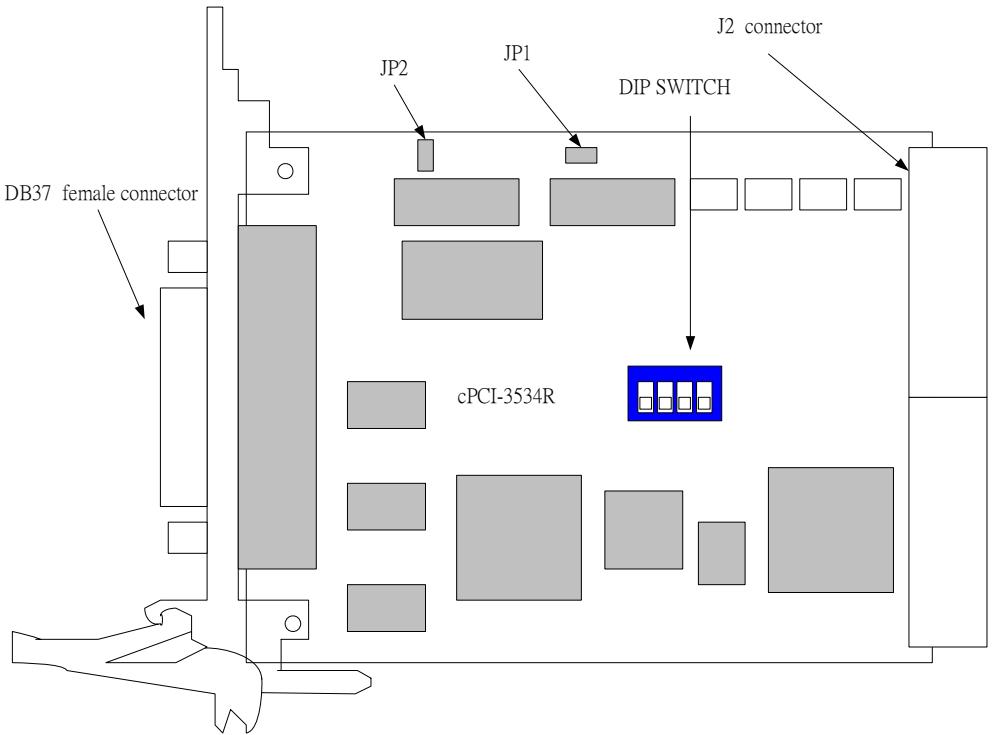
![DB37 female connector\nJP2\nJP1\nJ2 connector\nDIP SWITCH\ncPCI-3534R](.cpci-3534-3538-manual-3/28456eec9867109223971ccb1a615cb9e22fa0e8e2909f4f4f7a0c3113472186.jpg)

cPCI-3534R Profile

# 1.1.4 cPCI-3534 Connector Pin Assignment

DB37 female connector pin assignment for the cPCI-3534.

<table><tr><td>Pin No.</td><td>RS-232 Interface (Port A, B, C)</td><td>RS-422 Interface (Port D)</td><td>4S-485 Interface (Port D)</td></tr><tr><td>1</td><td>PortA_RXD(IN)</td><td></td><td></td></tr><tr><td>2</td><td>PortA_CTS(IN)</td><td></td><td></td></tr><tr><td>3</td><td>PortA_DSR(IN)</td><td></td><td></td></tr><tr><td>4</td><td>PortA_DCD(IN)</td><td></td><td></td></tr><tr><td>5</td><td>GND</td><td></td><td></td></tr><tr><td>6</td><td>PortB_TXD(OUT)</td><td></td><td></td></tr><tr><td>7</td><td>PortB_RTS(OUT)</td><td></td><td></td></tr><tr><td>8</td><td>PortB_DTR(OUT)</td><td></td><td></td></tr><tr><td>9</td><td>GND</td><td></td><td></td></tr><tr><td>10</td><td></td><td></td><td></td></tr><tr><td>11</td><td>GND</td><td></td><td></td></tr><tr><td>12</td><td>PortC_DTR(OUT)</td><td></td><td></td></tr><tr><td>13</td><td>PortC_RTS(OUT)</td><td></td><td></td></tr><tr><td>14</td><td>PortC_TXD(OUT)</td><td></td><td></td></tr><tr><td>15</td><td>GND</td><td colspan="2">PortD_Isolated GND</td></tr><tr><td>16</td><td></td><td></td><td></td></tr><tr><td>17</td><td></td><td>PortD_RXD-(IN)</td><td></td></tr><tr><td>18</td><td></td><td></td><td>D-</td></tr><tr><td>19</td><td></td><td>PortD_RXD+(IN)</td><td></td></tr><tr><td>20</td><td>PortA_TXD(OUT)</td><td></td><td></td></tr><tr><td>21</td><td>PortA_RTS(OUT)</td><td></td><td></td></tr><tr><td>22</td><td>PortA_DTR(OUT)</td><td></td><td></td></tr><tr><td>23</td><td>PortA_RI(IN)</td><td></td><td></td></tr><tr><td>24</td><td>PortB_RXD(IN)</td><td></td><td></td></tr><tr><td>25</td><td>PortB_CTS(IN)</td><td></td><td></td></tr><tr><td>26</td><td>PortB_DSR(IN)</td><td></td><td></td></tr><tr><td>27</td><td>PortB_DCD(IN)</td><td></td><td></td></tr><tr><td>28</td><td>PortB_RI(IN)</td><td></td><td></td></tr><tr><td>29</td><td>PortC_RI(IN)</td><td></td><td></td></tr><tr><td>30</td><td>PortC_DCD(IN)</td><td></td><td></td></tr><tr><td>31</td><td>PortC_DSR(IN)</td><td></td><td></td></tr><tr><td>32</td><td>PortC_CTS(IN)</td><td></td><td></td></tr><tr><td>33</td><td>PortC_RXD(IN)</td><td></td><td></td></tr><tr><td>34</td><td></td><td></td><td></td></tr><tr><td>35</td><td></td><td>PortD_TXD-(OUT)</td><td></td></tr><tr><td>36</td><td></td><td></td><td>D+</td></tr><tr><td>37</td><td></td><td>PortD_TXD+(OUT)</td><td></td></tr></table>

DB25 male connector pin assignment in the cPCI-3534 module for RS-232 interfaces (port A, B, and C) and the RS-422/485 interface (port D).

<table><tr><td>Pin No.</td><td>RS-232 Interface</td><td>RS-422 Interface</td><td>RS-485 Interface</td></tr><tr><td>2</td><td>TXD(OUT)</td><td>TXD+(OUT)</td><td></td></tr><tr><td>3</td><td>RXD(IN)</td><td>RXD+(IN)</td><td></td></tr><tr><td>4</td><td>RTS(OUT)</td><td></td><td>D+</td></tr><tr><td>5</td><td>CTS(IN)</td><td></td><td>D-</td></tr><tr><td>6</td><td>DSR(IN)</td><td>RXD- (In)</td><td></td></tr><tr><td>7</td><td>GND</td><td colspan="2">Isolated GND</td></tr><tr><td>8</td><td>DCD(IN)</td><td></td><td></td></tr><tr><td>20</td><td>DTR(OUT)</td><td>TXD- (Out)</td><td></td></tr></table>

DB9 male connector pin assignment in the cPCI-3534 module for RS-232 interfaces (port A, B and C) and the RS-422/485 interface (port D).

<table><tr><td>Pin No.</td><td>RS-232 Interface</td><td>RS-422 Interface</td><td>RS-485 Interface</td></tr><tr><td>1</td><td>DCD(IN)</td><td></td><td>.</td></tr><tr><td>2</td><td>RXD(IN)</td><td>RXD+(IN)</td><td></td></tr><tr><td>3</td><td>TXD(OUT)</td><td>TXD+(OUT)</td><td></td></tr><tr><td>4</td><td>DTR (OUT)</td><td>TXD-(OUT)</td><td></td></tr><tr><td>5</td><td>GND</td><td colspan="2">Isolated GND</td></tr><tr><td>6</td><td>DSR(IN)</td><td>RXD-(IN)</td><td></td></tr><tr><td>7</td><td>RTS(OUT)</td><td></td><td>D+</td></tr><tr><td>8</td><td>CTS(IN)</td><td></td><td>D-</td></tr><tr><td>9</td><td>RI(IN)</td><td></td><td></td></tr></table>

Compact PCI J2 connector pin assignment in cPCI-3534R module for RS-232/422/485 interfaces (cPCI-3534R only).

<table><tr><td>22</td><td>GND</td><td>GA4</td><td>GA3</td><td>GA2</td><td>GA1</td><td>GA0</td><td>GND</td></tr><tr><td>21</td><td>GND</td><td></td><td></td><td></td><td></td><td></td><td>GND</td></tr><tr><td>20</td><td>GND</td><td></td><td></td><td></td><td></td><td></td><td>GND</td></tr><tr><td>19</td><td>GND</td><td>FG</td><td>D+</td><td>D-</td><td>SG</td><td></td><td>GND</td></tr><tr><td>18</td><td>GND</td><td></td><td></td><td></td><td></td><td></td><td>GND</td></tr><tr><td>17</td><td>GND</td><td></td><td></td><td></td><td></td><td></td><td>GND</td></tr><tr><td>16</td><td>GND</td><td></td><td></td><td>TXD+</td><td>TXD-</td><td>SG</td><td>GND</td></tr><tr><td>15</td><td>GND</td><td>FG</td><td>RXD+</td><td>RXD-</td><td></td><td></td><td>GND</td></tr><tr><td>14</td><td>GND</td><td></td><td></td><td></td><td></td><td></td><td>GND</td></tr><tr><td>13</td><td>GND</td><td></td><td></td><td></td><td></td><td></td><td>GND</td></tr><tr><td>12</td><td>GND</td><td>DSR $^{3}$ </td><td>SG $^{3}$ </td><td>DCD $^{3}$ </td><td>DTR $^{3}$ </td><td></td><td>GND</td></tr><tr><td>11</td><td>GND</td><td>FG $^{3}$ </td><td>TX $^{3}$ </td><td>RX $^{3}$ </td><td>RTS $^{3}$ </td><td>CTS $^{3}$ </td><td>GND</td></tr><tr><td>10</td><td>GND</td><td></td><td></td><td></td><td></td><td></td><td>GND</td></tr><tr><td>9</td><td>GND</td><td></td><td></td><td></td><td></td><td></td><td>GND</td></tr><tr><td>8</td><td>GND</td><td>DSR $^{2}$ </td><td>SG $^{2}$ </td><td>DCD $^{2}$ </td><td>DTR $^{2}$ </td><td></td><td>GND</td></tr><tr><td>7</td><td>GND</td><td>FG $^{2}$ </td><td>TX $^{2}$ </td><td>RX $^{2}$ </td><td>RTS $^{2}$ </td><td>CTS $^{2}$ </td><td>GND</td></tr><tr><td>6</td><td>GND</td><td></td><td></td><td></td><td></td><td></td><td>GND</td></tr><tr><td>5</td><td>GND</td><td></td><td></td><td></td><td></td><td></td><td>GND</td></tr><tr><td>4</td><td>GND</td><td>DSR $^{1}$ </td><td>SG $^{1}$ </td><td>DCD $^{1}$ </td><td>DTR $^{1}$ </td><td></td><td>GND</td></tr><tr><td>3</td><td>GND</td><td>FG $^{1}$ </td><td>TX $^{1}$ </td><td>RX $^{1}$ </td><td>RTS $^{1}$ </td><td>CTS $^{1}$ </td><td>GND</td></tr><tr><td>2</td><td>GND</td><td></td><td></td><td></td><td></td><td></td><td>GND</td></tr><tr><td>1</td><td>GND</td><td></td><td></td><td></td><td></td><td></td><td>GND</td></tr><tr><td>Pin</td><td>Z</td><td>A</td><td>B</td><td>C</td><td>D</td><td>E</td><td>F</td></tr></table>

①Port A ②Port B ③Port C

# RS-232

FG : Frame Ground TX : Transmit Data

RX : Receive Data

RTS : Request to Send CTS : Clear to Send

DSR: Data Set Ready

SG : Signal Ground DCD : Data Carrier Detect

DTR: Data Terminal Ready

# RS-422

TXD+ : Transmit Data Positive

TXD- : Transmit Data Negative

RXD+ : Receive Data Positive

RXD- : Receive Data Negative

# RS-485

D+ : Data Signal Positive

D- : Data Signal Negative

# cPCI-R3534 Rear I/O Daughter Board (Rear I/O function only for cPCI3534R)

The cPCI-R3534 rear I/O daughter board provides a rear I/O connection transition, the connector and cable used in the rear is the same as the front.

DIP Switch and Jumper Setting

<table><tr><td>SW1</td><td>ON</td><td>OFF</td></tr><tr><td>SW1-1</td><td>Card1</td><td>Card2</td></tr><tr><td>SW1-4</td><td>RS-422</td><td>RS-485</td></tr></table>

The JP1 is for the RS422 terminator and the JP2 is for the RS-485 terminator. The terminator is ON while the jumper is ON.

# 1.2 cPCI-3544 Overview

# 1.2.1 What is the cPCI-3544?

The cPCI-3544 is an enhanced four ports serial communication module for industry communication interface RS-422/485 by Compact-PCI platform. It includes a PGA (Programmable Gate Array) to support the serial communication controller and a 37-pin connector to connect external I/O port from the front panel or using the rear I/O.

The expansion cable has four standard DB25 or DB9 connectors and one DB37 connector to connect with cPCI-3544 interface card.

The cPCI-R3544 transition board can support rear I/O connection by using one DB37 connector.

# 1.2.2 cPCI-3544 Features

• 32-bit CompactPCI 3U form factor
• PCI Rev.2.1 Plug and Play
- IRQ and I/O address automatically assigned by PCI Plug and Play
• Four communication ports intelligent buffer
• RS-422/485 hardware selectable
• RS-485 with auto direction flow control
• Channel to channel isolated industry communication port
• High speed communications concurrently (max. 115200 bps)
• Supports up to eight cards/32 ports per system
• Supports DOS, Windows 95/98, and Windows NT operation system

# 1.2.3 cPCI-3544 Specifications

• Compliant with PCI Spec.2.1
- Serial communication controller:
• 16C550A compatible
• 1.8432 - 7.3728 MHz
• System I/O mapping:

■ Assigned by PCI BIOS
- Shared IRQ

- Flow control
■ RS-485 auto direction

\- Port Capability:

■ Four isolated RS-422/485 port (DIP switch select)
■ Max. port per system: 32 (8 card)

• Isolation voltage: 500VDC
- Baud rate: Each port can be configured to 50 - 115,200 bps
• Operation System Compatibility: Windows 95/98/NT/QNX
- Connector: DB37 female connector
- Cable: External cable with four standard DB25(C425M) or DB9(C409M) male connector
• Operating temperature: 0 - 55 °C
• Storage temperature: -20 - 65 °C
• Humidity: 10% - 95%, non-condensing
• Dimension: $160 \times 100 \, mm^{2}$ ( $6.3 \times 3.9 \, in.^{2}$ ) 3U
• Power consumption: +5V @ 1400mA typical

![JP1~JP8\nJ2 connector\nDB37 female connector\ncPCI-3544R-XXX\nDIP SWITCH](.cpci-3534-3538-manual-3/c9dc306a8a9ac8f098d45c0e3e81f769929f39f8982d9587b5f742a10f19ddbc.jpg)

cPCI-3544R Profile

# 1.2.4 Connector Pin Assignment of cPCI-3544

DB37 female connector pin assignment for cPCI-3544.

<table><tr><td>Pin No.</td><td>RS-422 Interface</td><td>4S-485 Interface</td></tr><tr><td>1</td><td>PortA_RXD+(IN)</td><td></td></tr><tr><td>2</td><td></td><td>PortA_D+(I/O)</td></tr><tr><td>3</td><td>PortA_RXD-(IN)</td><td></td></tr><tr><td>4</td><td></td><td>PortA_D-(I/O)</td></tr><tr><td>5</td><td colspan="2">PortA_IsolatedGND</td></tr><tr><td>6</td><td>PortB_TXD+(OUT)</td><td></td></tr><tr><td>7</td><td>--</td><td></td></tr><tr><td>8</td><td>PortB_TXD-(OUT)</td><td></td></tr><tr><td>9</td><td colspan="2">PortB_Isolated GND</td></tr><tr><td>10</td><td colspan="2">--</td></tr><tr><td>11</td><td colspan="2">PortC_Isolated GND</td></tr><tr><td>12</td><td>PortC_TXD-(OUT)</td><td></td></tr><tr><td>13</td><td colspan="2">--</td></tr><tr><td>14</td><td>PortC_TXD+(OUT)</td><td></td></tr><tr><td>15</td><td colspan="2">PortD_Isolated GND</td></tr><tr><td>16</td><td></td><td>PortD_D-(I/O)</td></tr><tr><td>17</td><td>PortD_RXD-(IN)</td><td></td></tr><tr><td>18</td><td></td><td>PortD_D+(I/O)</td></tr><tr><td>19</td><td>PortD_RXD+(IN)</td><td></td></tr><tr><td>20</td><td>PortA_TXD+(OUT)</td><td></td></tr><tr><td>21</td><td>--</td><td></td></tr><tr><td>22</td><td>PortA_TXD-(OUT)</td><td></td></tr><tr><td>23</td><td>--</td><td></td></tr><tr><td>24</td><td>PortB_RXD+(IN)</td><td></td></tr><tr><td>25</td><td></td><td>PortB_D+(I/O)</td></tr><tr><td>26</td><td>PortB_RXD-(IN)</td><td></td></tr><tr><td>27</td><td></td><td>PortB_D-(I/O)</td></tr><tr><td>28</td><td colspan="2">--</td></tr><tr><td>29</td><td colspan="2">--</td></tr><tr><td>30</td><td></td><td>PortC_D-(I/O)</td></tr><tr><td>31</td><td>PortC_RXD-(IN)</td><td></td></tr><tr><td>32</td><td></td><td>PortC_D+(I/O)</td></tr><tr><td>33</td><td>PortC_RXD+(IN)</td><td></td></tr><tr><td>34</td><td colspan="2">--</td></tr><tr><td>35</td><td>PortD_TXD-(OUT)</td><td></td></tr><tr><td>36</td><td colspan="2">--</td></tr><tr><td>37</td><td>PortD_TXD+(OUT)</td><td></td></tr></table>

DB25 male connector pin assignment in cPCI-3544 module for RS-422/485 interface. (Port A - D)

<table><tr><td>Pin No.</td><td>RS-422 Interface</td><td>RS-485 Interface</td></tr><tr><td>2</td><td>TXD+</td><td></td></tr><tr><td>3</td><td>RXD+</td><td></td></tr><tr><td>5</td><td></td><td>D+</td></tr><tr><td>6</td><td>RXD-</td><td></td></tr><tr><td>7</td><td colspan="2">Each Port Isolated GND</td></tr><tr><td>8</td><td></td><td>D-</td></tr><tr><td>20</td><td>TXD-</td><td></td></tr></table>

DB9 male connector pin assignment in cPCI-3544 module for RS-422/485 interface. (Port A - D)

<table><tr><td>Pin No.</td><td>RS-422 Interface</td><td>RS-485 Interface</td></tr><tr><td>1</td><td></td><td>D-</td></tr><tr><td>2</td><td>RXD+</td><td></td></tr><tr><td>3</td><td>TXD+</td><td></td></tr><tr><td>4</td><td>TXD-</td><td></td></tr><tr><td>5</td><td colspan="2">Each Port Isolated GND</td></tr><tr><td>6</td><td>RXD-</td><td></td></tr><tr><td>8</td><td></td><td>D+</td></tr></table>

Compact PCI J2 connector pin assignment in cPCI-3544R module for RS-422/485 interface. (cPCI-3544R only)

<table><tr><td>22</td><td>GND</td><td>GA4</td><td>GA3</td><td>GA2</td><td>GA1</td><td>GA0</td><td>GND</td></tr><tr><td>21</td><td>GND</td><td></td><td></td><td></td><td></td><td></td><td>GND</td></tr><tr><td>20</td><td>GND</td><td></td><td></td><td></td><td></td><td></td><td>GND</td></tr><tr><td>19</td><td>GND</td><td></td><td>TXD-4</td><td></td><td>TXD+4</td><td></td><td>GND</td></tr><tr><td>18</td><td>GND</td><td>GND4</td><td>D-4</td><td>RXD-4</td><td>D+4</td><td>RXD+4</td><td>GND</td></tr><tr><td>17</td><td>GND</td><td></td><td></td><td></td><td></td><td></td><td>GND</td></tr><tr><td>16</td><td>GND</td><td></td><td></td><td></td><td></td><td></td><td>GND</td></tr><tr><td>15</td><td>GND</td><td></td><td></td><td></td><td></td><td></td><td>GND</td></tr><tr><td>14</td><td>GND</td><td></td><td>TXD-3</td><td></td><td>TXD+3</td><td></td><td>GND</td></tr><tr><td>13</td><td>GND</td><td>GND3</td><td>D-3</td><td>RXD-3</td><td>D+3</td><td>RXD+3</td><td>GND</td></tr><tr><td>12</td><td>GND</td><td></td><td></td><td></td><td></td><td></td><td>GND</td></tr><tr><td>11</td><td>GND</td><td></td><td></td><td></td><td></td><td></td><td>GND</td></tr><tr><td>10</td><td>GND</td><td></td><td></td><td></td><td></td><td></td><td>GND</td></tr><tr><td>9</td><td>GND</td><td></td><td>TXD-2</td><td></td><td>TXD+2</td><td></td><td>GND</td></tr><tr><td>8</td><td>GND</td><td>GND2</td><td>D-2</td><td>RXD-2</td><td>D+2</td><td>RXD+2</td><td>GND</td></tr><tr><td>7</td><td>GND</td><td></td><td></td><td></td><td></td><td></td><td>GND</td></tr><tr><td>6</td><td>GND</td><td></td><td></td><td></td><td></td><td></td><td>GND</td></tr><tr><td>5</td><td>GND</td><td></td><td></td><td></td><td></td><td></td><td>GND</td></tr><tr><td>4</td><td>GND</td><td></td><td>TXD-1</td><td></td><td>TXD+1</td><td></td><td>GND</td></tr><tr><td>3</td><td>GND</td><td>GND1</td><td>D-1</td><td>RXD-1</td><td>D+1</td><td>RXD+1</td><td>GND</td></tr><tr><td>2</td><td>GND</td><td></td><td></td><td></td><td></td><td></td><td>GND</td></tr><tr><td>1</td><td>GND</td><td></td><td></td><td></td><td></td><td></td><td>GND</td></tr><tr><td>Pin</td><td>Z</td><td>A</td><td>B</td><td>C</td><td>D</td><td>E</td><td>F</td></tr></table>

①Port A ②Port B ③Port C ④Port D

# RS-422

TXD+ : Transmit Data Positive

TXD- : Transmit Data Negative

RXD+ : Receive Data Positive

RXD- : Receive Data Negative

# RS-485

D+ : Data Signal Positive

D- : Data Signal Negative

# cPCI-R3544 Rear I/O Daughter Board (Rear I/O function only for cPCI-3544R)

The cPCI-R3544 rear I/O daughter board provides a rear I/O connection transition, the connector and cable used in the rear is the same as the front.

DIP Switch and Jumper Setting

<table><tr><td colspan="2">CARD NO.</td><td colspan="9">Port Select</td></tr><tr><td>SW1-3</td><td>#</td><td></td><td colspan="2">PortA</td><td colspan="2">PortB</td><td colspan="2">PortC</td><td colspan="2">PortD</td></tr><tr><td>000</td><td>0</td><td>SW</td><td>On</td><td>Off</td><td>On</td><td>Off</td><td>On</td><td>Off</td><td>On</td><td>Off</td></tr><tr><td>100</td><td>1</td><td>4</td><td>485</td><td>422</td><td></td><td></td><td></td><td></td><td></td><td></td></tr><tr><td>010</td><td>2</td><td>5</td><td></td><td></td><td>485</td><td>422</td><td></td><td></td><td></td><td></td></tr><tr><td>110</td><td>3</td><td>6</td><td></td><td></td><td></td><td></td><td>485</td><td>422</td><td></td><td></td></tr><tr><td>001</td><td>4</td><td>7</td><td></td><td></td><td></td><td></td><td></td><td></td><td>485</td><td>422</td></tr><tr><td>101</td><td>5</td><td colspan="9"></td></tr><tr><td>011</td><td>6</td><td colspan="9"></td></tr><tr><td>111</td><td>7</td><td colspan="9"></td></tr></table>

The JP1, JP3, JP5, JP7 is for the RS422 terminator and the JP2, JP4, JP6, JP8 is for the RS-485 terminator. The terminator is ON while the jumper is ON.

# 1.3 cPCI-3538 Overview

# 1.3.1 What is the cPCI-3538?

The cPCI-3538 is an enhanced eight ports serial communication card used for cPCI platform. It includes a PGA (Programmable Gate Array), which supports the serial communication controller, and a 62-pin connector which connects external I/O port on the front panel or the rear I/O.

The expansion cable has eight standard DB25 connectors and one DB62 connector to connect to cPCI-3538 interface card. User may also use one DB62 to DB62 cable to connect between one cPCI-3538 and C588XB for providing 8 channel isolated RS-232/422/485 interface.

The cPCI-R3538 transition board can support rear I/O connection by using one DB62 connector.

# 1.3.2 Feature of cPCI-3538

• 32-bit CompactPCI 3U form factor
• PCI Rev.2.1 Plug and Play
- IRQ and I/O address automatically assigned by PCI Plug and Play
• Eight communication ports intelligent buffer
• High Speed Communication (max. 115200 bps)
- Suitable for modems, data display, data collection, telecommunication
• Supports up to 2 cards/8 ports per system
- Supports DOS, Windows 3.1, Windows 95/98, and Window NT operation system
- Optional isolated RS-232/422/485 interface for each port independently by C888XB

# 1.3.3 Specification of cPCI-3538

• Compliant with PCI Spec.2.1
- Serial communication controller:
■ 16C550A compatible
■ 1.8432 - 7.3728 MHz

• System I/O mapping:

■ Assigned by PCI BIOS
- Shared IRQ

\- Flow control

Xon/Xoff control
■ RTS/CTS control

\- Port Capability:

■ Eight independent RS-232C compatible ports
■ Optional external C588XB box for extending to eight isolated RS-232/422/485 port
■ Max. port per system: 16 (2 card)

\- Baud rate: Each port can be configured to 50 - 115,200 bps

\- Operation System Compatibility: DOS, Windows 3.1, and Windows 95/98/NT

\- Connector: DB62 female connector

• Cable: External cable with 8 standard DB25 male connector

• Operating temperature: 0 - 55 °C

• Storage temperature: -20 - 65 °C

• Humidity: 10% - 95%, non-condensing

• Dimension: 160 x 100 mm $^{2}$ (6.3 x 3.9 in. $^{2}$ ) 3U

• Power consumption: +5V @ 1400mA typical

![DB62 female connector\nJ2 connector\ncPCI-3538R\nJP1](.cpci-3534-3538-manual-3/0e91202130f1056bf24d6e810bedb8f4ad75b1e32f010a1b4d6c8772f5980f8d.jpg)

cPCI-3538R Profile

# 1.3.4 Connector Pin Assignment of cPCI-3538

DB62 female connector pin assignment for cPCI-3538.

<table><tr><td>Pin No.</td><td>Signal Name</td><td>Pin No.</td><td>Signal Name</td></tr><tr><td>1</td><td>PortA_TXD (OUT)</td><td>32</td><td>PortG_CTS(IN)</td></tr><tr><td>2</td><td>PortA_RXD (IN)</td><td>33</td><td>PortG_DSR(IN)</td></tr><tr><td>3</td><td>PortA_RTS (OUT)</td><td>34</td><td>PortG_DTR(OUT)</td></tr><tr><td>4</td><td>PortA_CTS (IN)</td><td>35</td><td>PortG_DCD(IN)</td></tr><tr><td>5</td><td>PortA_DSR (IN)</td><td>36</td><td>PortF_TXD(OUT)</td></tr><tr><td>6</td><td>PortA_DTR (OUT)</td><td>37</td><td>PortF_RXD(IN)</td></tr><tr><td>7</td><td>PortA_DCD (IN)</td><td>38</td><td>PortF_RTS(OUT)</td></tr><tr><td>8</td><td>PortC_TXD(OUT)</td><td>39</td><td>PortF_CTS(IN)</td></tr><tr><td>9</td><td>PortC_RXD(IN)</td><td>40</td><td>PortF_DSR(IN)</td></tr><tr><td>10</td><td>PortC_RTS(OUT)</td><td>41</td><td>PortF_DTR(OUT)</td></tr><tr><td>11</td><td>PortC_CTS(IN)</td><td>42</td><td>PortF_DCD(IN)</td></tr><tr><td>12</td><td>PortC_DSR(IN)</td><td>43</td><td>GND</td></tr><tr><td>13</td><td>PortC_DTR(OUT)</td><td>44</td><td>GND</td></tr><tr><td>14</td><td>PortC_DCD(IN)</td><td>45</td><td>GND</td></tr><tr><td>15</td><td>PortE_TXD(OUT)</td><td>46</td><td>PortD_TXD(OUT)</td></tr><tr><td>16</td><td>PortE_RXD(IN)</td><td>47</td><td>PortD_RXD(IN)</td></tr><tr><td>17</td><td>PortE_RTS(OUT)</td><td>48</td><td>PortD_RTS(OUT)</td></tr><tr><td>18</td><td>PortE_CTS(IN)</td><td>49</td><td>PortD_CTS(IN)</td></tr><tr><td>19</td><td>PortE_DSR(IN)</td><td>50</td><td>PortD_DSR(IN)</td></tr><tr><td>20</td><td>PortE_DTR(OUT)</td><td>51</td><td>PortD_DTR(OUT)</td></tr><tr><td>21</td><td>PortE_DCD5(IN)</td><td>52</td><td>PortD_DCD(IN)</td></tr><tr><td>22</td><td>PortB_TXD(OUT)</td><td>53</td><td>PortH_TXD(OUT)</td></tr><tr><td>23</td><td>PortB_RXD(IN)</td><td>54</td><td>PortH_RXD(IN)</td></tr><tr><td>24</td><td>PortB_RTS(OUT)</td><td>55</td><td>PortH_RTS(OUT)</td></tr><tr><td>25</td><td>PortB_CTS(IN)</td><td>56</td><td>PortH_CTS(IN)</td></tr><tr><td>26</td><td>PortB_DSR(IN)</td><td>57</td><td>PortH_DSR(IN)</td></tr><tr><td>27</td><td>PortB_DTR(OUT)</td><td>58</td><td>PortH_DTR(OUT)</td></tr><tr><td>28</td><td>PortB_DCD(IN)</td><td>59</td><td>PortH_DCD(IN)</td></tr><tr><td>29</td><td>PortG_TXD(OUT)</td><td>60</td><td>GND</td></tr><tr><td>30</td><td>PortG_RXD(IN)</td><td>61</td><td>GND</td></tr><tr><td>31</td><td>PortG_RTS(OUT)</td><td>62</td><td>GND</td></tr></table>

DB25 male connector pin assignment in the cPCI-3538 module for RS-232 interfaces (port A-H).

<table><tr><td>Pin No.</td><td>Signal Name</td></tr><tr><td>2</td><td>TXD(OUT)</td></tr><tr><td>3</td><td>RXD(IN)</td></tr><tr><td>4</td><td>RTS(OUT)</td></tr><tr><td>5</td><td>CTS(IN)</td></tr><tr><td>6</td><td>DSR(IN)</td></tr><tr><td>7</td><td>GND</td></tr><tr><td>8</td><td>DCD(IN)</td></tr><tr><td>20</td><td>DTR(OUT)</td></tr></table>

DB9 male connector pin assignment in the cPCI-3538 module for RS-232 interfaces (port A - H).

<table><tr><td>Pin No.</td><td>Signal Name</td></tr><tr><td>1</td><td>DCD(IN)</td></tr><tr><td>2</td><td>RXD(IN)</td></tr><tr><td>3</td><td>TXD(OUT)</td></tr><tr><td>4</td><td>DTR (OUT)</td></tr><tr><td>5</td><td>GND</td></tr><tr><td>6</td><td>DSR(IN)</td></tr><tr><td>7</td><td>RTS(OUT)</td></tr><tr><td>8</td><td>CTS(IN)</td></tr></table>

Compact PCI J2 connector pin assignment in cPCI-3538R module for RS-232 interface. (cPCI-3538R only)

<table><tr><td>22</td><td>GND</td><td>GA4</td><td>GA3</td><td>GA2</td><td>GA1</td><td>GA0</td><td>GND</td></tr><tr><td>21</td><td>GND</td><td></td><td></td><td></td><td></td><td></td><td>GND</td></tr><tr><td>20</td><td>GND</td><td>DSR8</td><td>DCD8</td><td>DTR8</td><td>RTS8</td><td>CTS8</td><td>GND</td></tr><tr><td>19</td><td>GND</td><td>FG8</td><td>TX8</td><td>RX8</td><td>SG8</td><td></td><td>GND</td></tr><tr><td>18</td><td>GND</td><td>FG7</td><td>TX7</td><td>RX7</td><td>SG7</td><td></td><td>GND</td></tr><tr><td>17</td><td>GND</td><td>DSR7</td><td>DCD7</td><td>DTR7</td><td>RTS7</td><td>CTS7</td><td>GND</td></tr><tr><td>16</td><td>GND</td><td></td><td></td><td></td><td></td><td></td><td>GND</td></tr><tr><td>15</td><td>GND</td><td>DSR6</td><td>DCD6</td><td>DTR6</td><td>RTS6</td><td>CTS6</td><td>GND</td></tr><tr><td>14</td><td>GND</td><td>FG6</td><td>TX6</td><td>RX6</td><td>SG6</td><td></td><td>GND</td></tr><tr><td>13</td><td>GND</td><td>FG5</td><td>TX5</td><td>RX5</td><td>SG5</td><td></td><td>GND</td></tr><tr><td>12</td><td>GND</td><td>DSR5</td><td>DCD5</td><td>DTR5</td><td>RTS5</td><td>CTS5</td><td>GND</td></tr><tr><td>11</td><td>GND</td><td></td><td></td><td></td><td></td><td></td><td>GND</td></tr><tr><td>10</td><td>GND</td><td>DSR4</td><td>DCD4</td><td>DTR4</td><td>RTS4</td><td>CTS4</td><td>GND</td></tr><tr><td>9</td><td>GND</td><td>FG4</td><td>TX4</td><td>RX4</td><td>SG4</td><td></td><td>GND</td></tr><tr><td>8</td><td>GND</td><td>FG3</td><td>TX3</td><td>RX3</td><td>SG3</td><td></td><td>GND</td></tr><tr><td>7</td><td>GND</td><td>DSR3</td><td>DCD3</td><td>DTR3</td><td>RTS3</td><td>CTS3</td><td>GND</td></tr><tr><td>6</td><td>GND</td><td></td><td></td><td></td><td></td><td></td><td>GND</td></tr><tr><td>5</td><td>GND</td><td>DSR2</td><td>DCD2</td><td>DTR2</td><td>RTS2</td><td>CTS2</td><td>GND</td></tr><tr><td>4</td><td>GND</td><td>FG2</td><td>TX2</td><td>RX2</td><td>SG2</td><td></td><td>GND</td></tr><tr><td>3</td><td>GND</td><td>FG1</td><td>TX1</td><td>RX1</td><td>SG1</td><td></td><td>GND</td></tr><tr><td>2</td><td>GND</td><td>DSR1</td><td>DCD1</td><td>DTR1</td><td>RTS1</td><td>CTS1</td><td>GND</td></tr><tr><td>1</td><td>GND</td><td></td><td></td><td></td><td></td><td></td><td>GND</td></tr><tr><td>Pin</td><td>Z</td><td>A</td><td>B</td><td>C</td><td>D</td><td>E</td><td>F</td></tr></table>

RS-232

<table><tr><td>FG</td><td>:</td><td>Frame Ground</td><td>TX</td><td>:</td><td>Transmit Data</td></tr><tr><td>RX</td><td>:</td><td>Receive Data</td><td></td><td></td><td></td></tr><tr><td>RTS</td><td>:</td><td>Request to Send</td><td>CTS</td><td>:</td><td>Clear to Send</td></tr><tr><td>DSR</td><td>:</td><td>Data Set Ready</td><td></td><td></td><td></td></tr><tr><td>SG</td><td>:</td><td>Signal Ground</td><td>DCD</td><td>:</td><td>Data Carrier Detection</td></tr><tr><td>DTR</td><td>:</td><td>Data Terminal Ready</td><td></td><td></td><td></td></tr></table>

cPCI-R3538 Rear I/O Daughter Board (Rear I/O function only for cPCI-3538R)

The cPCI-R3538 rear I/O daughter board provides a rear I/O connection transition; the connector and cable used in the rear are the same as the front.

# 2

# Installation

This chapter describes the configurations of the serial communication module. The contents in the package and unpacking information that the user should be aware of are described in the beginning. The serial communication modules are Plug and Play and very easy to install into cPCI system.

# 2.1 What You Have

In addition to this User's Manual, the package includes the following items:

• cPCI-3534/3544/3538 Serial Communication Interface Module
• Expansion Cable (C425M, C409M or C825M, C809M)
• R-3534/3538 Rear I/O Daughter Board (For the rear I/O version)
- “ADLINK All-in-One Compact Disc” or Disks

If any of these items are missing or damaged, contact the dealer from whom the product was purchased. Save the shipping materials and carton in case the products needs to be shipped or stored in the future.

# 2.2 Unpacking

Your serial communication module contains sensitive electronic components that can be easily damaged by static electricity.

The module should be done on a grounded anti-static mat. The operator should be wearing an anti-static wristband, grounded at the same point as the anti-static mat.

Inspect the module carton for obvious damage. Shipping and handling may cause damage to your module. Ensure there are no shipping and handling damages on the module before processing.

After opening the module carton, remove the system module and place it only on a grounded anti-static surface component side up.

Again inspect the module for damage. Press down on all socket IC's to ensure they are properly seated. Do this only with the module placed on a firm flat surface.

Note: DO NOT APPLY POWER TO THE MODULE IF IT HAS BEEN DAMAGED.

You are now ready to install your cPCI Module.

# 2.3 Installation Procedure

1. Turn off your cPCI computer system.
2. Turn off all accessories (printer, modem, monitor, etc.) connected to computer.
3. Select a cPCI slot.
4. Before handling the serial communication module, discharge any static buildup on your body by touching the metal case of the computer. Hold the edge and do not touch the components.
5. Position the module into the cPCI slot selected.
6. Secure the module in place of the system.

# 2.4 Hardware Configuration

The serial communication module has Plug and Play component, the card can requests memory usage (I/O port locations) of the card which is assigned by system BIOS. The address assignment is done on a board-by-board basis for all serial communication cards in the system.

The jumper SW1-1 for cPCI-3534 and the JP1 for cPCI-3538 is used for the system to recognize the first or second card of the same model in the system if there are two of the same cards on the board.

The SW1-3 for cPCI-3544 is used for the system to recognize the card number of the same model in the system if there are more than two cards of the same on board.

# 2.4.1 Wiring Example

You can use the C425M and C409M for wiring. Please refer to Chapter 1 for pin assignment.

# 2.5 Software Installation

# 2.5.1 Windows NT Installation

Once Windows NT system has been started, login using an account with administrative right.

1. Start the [Control Panel] applet by double clicking the icon in the [Program Managers] main group.
2. In the [Control Panel] applet, double click [Network] icon to bring up the Network Control Panel Applet (NCPA).
3. Within the NCPA, select the [Add Adaptor] button, a list of possible adaptors should be displayed. Go to the end of this list and select &lt;Other&gt; requires disk from manufacturer.
4. When prompted for the path, specify the drive and directory where the NCPA can find the new driver for the card installed.

For cPCI-3534, specify as follows:

X:\NuCOM\CPCI3534\NT4

For cPCI-3544, specify as follows:

X:\NuCOM\CPCI3544\NT4

For cPCI-3538, specify as follows:

X:\NuCOM\CPCI3538\NT4

(Where X indicates CD-ROM drive)

1. Follow the configuration dialog boxes to install the driver.
2. In the default condition, the TTY port is given name from "COM3". User can specify the start "COM" port number in installation procedure.
3. We can install up to two same type serial communication cards in one NT system.

4. When two of the same type of serial communication cards are required to be installed in one NT system, confirm to let one card's SW1-1 is ON while the other card's SW1-1 is OFF for cPCI-3534 and JP1 is ON while the other card's JP1 is OFF for cPCI-3538. The same applies to cPCI-3544 with SW1-3 adjusting to a different number.
5. The card with switch ON will have a low COM port number. The card with switch OFF will have a higher COM port number than the former.
6. If two of the same type of serial communication modules are installed with switch ON or OFF simultaneously, it cannot be certain that the system will function properly.
7. If you install multiple cards onto one NT system simultaneously, ensure that the COM port number assigned is not the same as the one used for a different card. Otherwise, the system may not function properly.
8. To avoid confusion of the NT system's COM port number, it is suggested that the switch ON for the first card be installed in NT system.
9. After installing the driver, reboot the PC, where more COM ports are available.
10. If our NT driver has been previously installed in the system before, remove this driver first, then install our new version driver. Otherwise, the user may encounter some problems with the system.

# 2.5.2 Windows 95/98 Installation

Once Windows 95/98 system has been started, the Plug and Play function in 95/98 system will find the new serial communication card. If this is the first time installing a serial communication card on the Windows 95/98 system, the user will be prompted to install the driver. Follow the instructions to input the COM port number starting value for the first and second cards.

Because the resource will be assigned by PCI BIOS, It is relatively difficult to check which card is first or second from resource. The switch will assign the COM port number for each card for the system.

After installing the driver, the user may be informed that new hardware has been found. The driver does not need to be installed again, Windows 95/98 will add the COM port automatically.

1. You can install up to two cPCI-3534/3538 cards on one 95/98 system.
2. When two of the same type of cards are required to be installed on one 95/98 system, confirm to let one card's switch to be ON, and the other card's switch OFF.
3. The card with switch ON will have COM port number assigned for the first card. The card with switch OFF will have COM port number assigned for second card.
4. If two of the same type of serial communication cards are installed with switch ON or OFF simultaneously, it cannot be certain that they system will function properly.
5. If multiple cards are installed on one 95/98 system simultaneously, ensure that the COM port number assigned to one card is not used for a different card, otherwise the system may fail to function properly.
6. To avoid confusion of the 95/98 system's COM port number, it is suggested that the switch ON for the first card be installed in 95/98 system
7. The serial communication card can be used in interrupt shared mode. PCI BIOS will assign IRQ for each serial communication card. For multi-card applications, one IRQ can be used in each card, but the user must ensure that the system has a minimum of one

IRQ left for P&P function. If there are no IRQs left to be assigned to the serial communication card, there may be errors in the operation.

# 2.5.3 Windows 2000/XP Installation

Once the Windows 2000/XP system has been started, the Plug and Play function in 2000/XP system will find the new cPCI-3534/3538/3544 card. If this is the first time installing drivers on your 2000/XP system, a dialogue box will instruct the user to install the driver. Follow the instructions below to specify the driver location.

For cPCI-3534/3538

X:\SerialComm\cPCI-353X\Win2000-XP; X is the CD-ROM For cPCI-3544

X: \SerialComm\cPCI-3544W2000; X is the CD-ROM

As the resource will be assigned by PCI BIOS, it is relatively difficult to check which card is first card or second card from resource. For this reason, ADLINK has placed a jumper in each cPCI-3534/3538 card to set the first card or second card for this these comport cards. (cPCI-3544 does not include this function). The COM port number can now be fixed for each card. This is very important for cPCI-3534/3538 card.

# 2.5.4 LINUX Driver Installation

Installation for cPCI-3534/3538 Linux Driver

1. Copy the "alnxsrc.Z" file onto the Linux system. (alnxsrc.Z is located in "X:\SerialComm \cPCI-353X \Linux" directory; X is the CD-ROM.)

2. Uncompress the file to retrieve the original diskette image file "alnxsrc".
uncompress alnxsrc

3. Use the "dd" command to duplicate the diskette.
dd if=alnxsrc of=/dev/fd0

4. Please "tar" this diskette in root directory.
cd /
tar xvf /dev/fd0

5. Please install driver in /etc/rayon directory.
cd /etc/rayon
./Install

6. Select the target card type to install driver.
The kernel source file is vital, and can be found in the /usr/src/linux directory. Some Linux distribution systems may have a different directory name. Please link to /usr/src/linux name.

Installation for cPCI-3544 Linux Driver

# 1. UNPACK

Decompress the pci3544.tgz (pci3544.tgz is located in

"X:\SerialComm \cPCI-3544 \Linux" directory; X is the CD-ROM.)): tar xvzf pci3544.tgz

This will extract the 'cPCI\_3544' directory in the Linux.

There are two subdirectories as follows:

drivers/ contains the device module and the installation script util/ the utility for the 422/485 mode setting

# 2. INSTALL DEVICE

Because of the cPCI-bus architecture, the cPCI-3544 devices can be detected automatically. All that is required of the user is to insert modules and to make nodes for the devices.

This can be done manually, or use our installation script below for driver installation.

./&lt;InstallDir&gt;/pci\_3544/drivers/3544\_inst.pl

Execute the installation script without any parameters, the usage is displayed as follows:

# Usage:

3544\_inst.pl -cards num\_of\_3544 -tty TTY\_MAJOR -cua CALLOUT\_MAJOR -path installed\_dir

num\_of\_3544: number of pci3544 installed

TTY\_MAJOR: the Major number for serial ports of cPCI-3544i (optional)

CALLOUT\_MAJOR: the Major number for cPCI-3544 callout ports (optional)

installed\_dir: the dir. cPCI-3544 installed (optional)

The optional parameter '-tty' and '-cua' are used to indicate the major number for TTY serial ports and Callout ports. The user can assign the major number for TTY and Callout ports, or use the default setting (70/71) for these ports.

To install the driver for three cPCI-3544 cards, execute the script as follows:

./3544\_inst.pl -cards 3 -tty 70 -cua 71 -path &lt;installed dir.&gt; or simply execute the following command if the device module is in the current directory.

./3544\_inst.pl -cards 3

The optional parameter '-path' is used to indicate the directory of pci-3544package. If the cPCI-3544 driver can not be found in working directory, the optional parameter '-path' is required.

./3544\_inst.pl -cards 2 -path /usr/local/pci\_3544

After installing the devices successfully, the ports of cPCI-3544 can be used as the normal serial ports supported by Linux.

# 2.5.5 Windows 95/98/NT Utility Diagram for cPCI-3544

The cPCI-3534/3538 does not require any configuration utility. It is similar to the system COM ports.

The cPCI-3544 is a 4-Port RS-422/485 serial communication module. It supports the software configuration for RS-422/485. When choosing the RS-422 mode, the RS-485 port would be disabled automatically. AdlComSet.exe can be used for configuration.

![ADLINK COM Devices Information\nRegistered ADLINK COM devices:\nBoard Type (ID) COM\nCPCI3544 (#7) COM5-COM8\nCPCI3544 (#0) COM5-COM8\nPress 'Port Setting' button to set the\nstarting COM port Number ...\nOK Cancel Port Setting...\nExisting Cards and\nits port distribution\nPress here for COM\nPort Number Setting](.cpci-3534-3538-manual-3/476b7af52f5b8556aa46abda6cab89b8bc4f9f7ea80d74e145cb30ed626c2788.jpg)

![COM Port Number Setting\nBoard Type: CPCI3544\nPort# COM Number Mode\n0 COM5 RS-422\n1 COM6 RS-485\n2 COM7 RS-485\n3 COM8 RS-485\nStarting COM# COM5\nMode Setting RS-422\nKeep Port Mode\nOK Cancel\nExisting Cards and its port distribution\nThe first one port maps to system port.\nPort mode\nWhen checked, the configuration will be true after rebooting.\nIf it is not checked, after rebooting, the port mode will follow the DIP switch configuration.](.cpci-3534-3538-manual-3/48767433bcee3f7aa81a1801df91bba452dfe420455dfe5778738062bbf21b09.jpg)

# 2.6 AP Examples

Follow the installation guide above first.

# 2.6.1 Dos Environment

For cPCI-3534/3538, please refer to the README file included in the driver.

The cPCI-3544 does not provide the DOS library. If the user wishes to program by themselves, contact the dealer from whom the product was purchased, or the service mailbox in ADLINK.

# 2.6.2 Windows (Windows 95/98/NT) Environment

Extra ports can be found in the system control panel after installing the driver. Programming can be performed as per COM port. Please refer to the sample programs in the driver.

# 2.6.3 Linux Environment

The sample program can be found in the driver.

# Warranty Policy

Thank you for choosing ADLINK. To understand your rights and enjoy all the after-sales services we offer, please read the following carefully.

1. Before using ADLINK's products please read the user manual and follow the instructions exactly. When sending in damaged products for repair, please attach an RMA application form which can be downloaded from: http://rma.adlinktech.com/policy/.
2. All ADLINK products come with a limited two-year warranty, one year for products bought in China.

- The warranty period starts on the day the product is shipped from ADLINK's factory.
- Peripherals and third-party products not manufactured by ADLINK will be covered by the original manufacturers' warranty.
- For products containing storage devices (hard drives, flash cards, etc.), please back up your data before sending them for repair. ADLINK is not responsible for any loss of data.
- Please ensure the use of properly licensed software with our systems. ADLINK does not condone the use of pirated software and will not service systems using such software. ADLINK will not be held legally responsible for products shipped with unlicensed software installed by the user.
- For general repairs, please do not include peripheral accessories. If peripherals need to be included, be certain to specify which items you sent on the RMA Request & Confirmation Form. ADLINK is not responsible for items not listed on the RMA Request & Confirmation Form.

3. Our repair service is not covered by ADLINK's guarantee in the following situations:

\- Damage caused by not following instructions in the User's Manual.

- Damage caused by carelessness on the user's part during product transportation.
- Damage caused by fire, earthquakes, floods, lightening, pollution, other acts of God, and/or incorrect usage of voltage transformers.
- Damage caused by inappropriate storage environments such as with high temperatures, high humidity, or volatile chemicals.
- Damage caused by leakage of battery fluid during or after change of batteries by customer/user.
- Damage from improper repair by unauthorized ADLINK technicians.
- Products with altered and/or damaged serial numbers are not entitled to our service.
• This warranty is not transferable or extendible.
- Other categories not protected under our warranty.

4. Customers are responsible for all fees necessary to transport damaged products to ADLINK.

For further questions, please e-mail our FAE staff: service@adlinktech.com
[🔗 Link to the original document](.cpci-3534-3538-manual-3/cpci-3534-3538-manual-3.pdf)
