# cPCI-3620 Series

Low-Power 3U CompactPCI®

Quad-Core Intel® Atom™ Processor Blade

# User’s Manual

![Back view of an electronic device module with visible circuit boards, ports, and connectors (no readable text or symbols)](.cpci-3620-50m-15098-2010-11/b9b3d3143e570007b8a3a0d499e7bf9372414c3432ebf6e016544911618427a6.jpg)

Manual Rev.: 1.1

Revision Date: March 17, 2025

Part No: 50M-15098-2010

Revision History

<table><tr><td>Revision</td><td>Release Date</td><td>Description of Change(s)</td></tr><tr><td>1.0</td><td>16/02/2016</td><td>Initial release</td></tr><tr><td>1.1</td><td>17/03/2025</td><td>Faceplate layouts updated</td></tr></table>

# Preface

# Copyright 2016, 2025 ADLINK Technology Inc.

This document contains proprietary information protected by copyright. All rights are reserved. No part of this manual may be reproduced by any mechanical, electronic, or other means in any form without prior written permission of the manufacturer.

# Disclaimer

The information in this document is subject to change without prior notice in order to improve reliability, design, and function and does not represent a commitment on the part of the manufacturer.

In no event will the manufacturer be liable for direct, indirect, special, incidental, or consequential damages arising out of the use or inability to use the product or documentation, even if advised of the possibility of such damages.

# Environmental Responsibility

ADLINK is committed to fulfill its social responsibility to global environmental preservation through compliance with the European Union's Restriction of Hazardous Substances (RoHS) directive and Waste Electrical and Electronic Equipment (WEEE) directive. Environmental protection is a top priority for ADLINK. We have enforced measures to ensure that our products, manufacturing processes, components, and raw materials have as little impact on the environment as possible. When products are at their end of life, our customers are encouraged to dispose of them in accordance with the product disposal and/or recovery programs prescribed by their nation or company.

# Trademarks

Product names mentioned herein are used for identification purposes only and may be trademarks and/or registered trademarks of their respective companies.

# Conventions

Take note of the following conventions used throughout this manual to make sure that users perform certain tasks and instructions properly.

![The image displays a simple graphic icon featuring a large red checkmark overlaid on a white, lined piece of paper.](.cpci-3620-50m-15098-2010-11/ac65c19f3c4039bce5a95d395bc64cc36c94241663f18a8e4593aa9cbb77b47b.jpg)
NOTE:

Additional information, aids, and tips that help users perform tasks.

![A yellow triangular warning sign with a black border and a large black exclamation mark in the center.](.cpci-3620-50m-15098-2010-11/c9bc5ce8e47b773505bb8934559a49c164f1a0e0d1c33940d4de8524e515a905.jpg)
CAUTION:

Information to prevent minor physical injury, component damage, data loss, and/or program corruption when trying to complete a task.

![This image displays a standard warning sign featuring a red triangle with a white border, containing a large white exclamation point in the center.](.cpci-3620-50m-15098-2010-11/4af7a9415473facb25a156123a218f7eebe1e66c29bf576943de5c4518f7d46e.jpg)
WARNING:

Information to prevent serious physical injury, component damage, data loss, and/or program corruption when trying to complete a specific task.

# Table of Contents

# Revision History....... ii

# Preface ............ iii

# List of Figures ....... ix

# List of Tables ........ .. xi

# 1 Introduction .....

1.1 Overview.... T
1.2 Features... 2
1.3 Model Number Decoder... 3
1.4 Package Contents ..... 5

# 2 Specifications ........ 7

2.1 cPCI-3620 Processor Blade Specifications ..... 7
2.2 cPCI-R3610(T) RTM Specifications...... 9
2.3 Block Diagrams... 10
2.4 I/O Connectivity Table . 13
2.5 Power Requirements ... 14

# 3 Functional Description ...... 17

3.1 Processors..... 17
3.2 PMC/XMC.... 19
3.3 Intel® Virtualization Technology .. 19
3.4 Intel® AES New Instructions.... 1 9
3.5 Battery ........ . 20

# 4 Board Interfaces ....... . 21

4.1 cPCI-3620 Series Board Layout .. 21
4.2 cPCI-3620 Blade Assembly Layout ... 22

4.3 cPCI-3620D Blade Assembly Layout... 2 3
4.4 cPCI-3620T Blade Assembly Layout .. . 24
4.5 cPCI-3620N Blade Assembly Layout.. 2 5
4.6 cPCI-3620 Series Faceplate...... . 26
4.7 cPCI-R3610(T) RTM Board Layout.. 2 9
4.8 cPCI-R3610(T) RTM Faceplate ... 3 0
4.9 Connector Pin Assignments.... 31
4.10 Jumper Settings.... 47

# 5 Getting Started ....... .. 49

5.1 CPU and Heatsink .. 49
5.2 SATA Drive Installation.. 50
5.3 PMC/XMC Card Installation ..... 52
5.4 Installing the cPCI-3620 to the Chassis.... 53
5.5 RTM Installation - cPCI-R3610(T).. 54

# 6 Driver Installation...... ... 55

6.1 cPCI-3620 Drivers.... . 55

# 7 Utilities ...... .. 57

7.1 SEMA.. 57
7.2 Preboot Execution Environment (PXE)........ 57
7.3 Watchdog Timer.... 58

# 8 BIOS Setup Utility ........ .... 59

8.1 Starting the BIOS .... 59
8.2 Main Setup......... 62
8.3 Advanced BIOS Setup..... 65

8.3.1 Super IO Configuration .. .. 66
8.3.2 Serial Port Console Redirection. .. 67
8.3.3 CPU Configuration ...... .. 70
8.3.4 PPM Configuration.... . 72
8.3.5 Thermal Configuration .. .. 73
8.3.6 IDE Configuration . . 74

8.3.7 Network Stack Configuration ..... .. 75
8.3.8 CSM Configuration ..... .. 76
8.3.9 USB Configuration.... . 77

8.4 Chipset Configuration ...... 78

8.4.1 North Bridge..... .. 78

8.4.2 South Bridge. .. 80

8.5 Security .... 82

8.6 Boot Settings .. 83

8.7 Save & Exit Menu .. 84

# Important Safety Instructions ...... 87

# Getting Service........ 89

This page intentionally left blank.

# List of Figures

Figure 2-1: cPCI-3620 Blade Functional Block Diagram............. ... 10

Figure 2-2: cPCI-3620D Daughter Board Functional Block Diagram11

Figure 2-3: cPCI-3620T Daughter Board Functional Block Diagram11

Figure 2-4: cPCI-R3610 RTM Functional Block Diagram ................ 12

Figure 4-1: cPCI-3620 Series Board Layout .... .. 21

Figure 4-2: cPCI-3620 Blade Assembly Layout ... . 22

Figure 4-3: cPCI-3620D Blade Assembly Layout... .. 23

Figure 4-4: cPCI-3620T Blade Assembly Layout.. . 24

Figure 4-5: cPCI-3620N Blade Assembly Layout... . 25

Figure 4-6: cPCI-3620, cPCI-3620D/N Faceplate Layout.... ..... 26

Figure 4-7: cPCI-3620T/S Faceplate Layout.... .. 27

Figure 4-8: cPCI-R3610(T) RTM Board Layout . .. 29

Figure 4-9: cPCI-R3610(T) RTM Faceplate.. .. 30

This page intentionally left blank.

# List of Tables

Table 2-1: cPCI-3620 Processor Blade Specifications .. 7

Table 2-2: cPCI-R3610(T) RTM Specifications.... 9

Table 2-3: cPCI-3620 I/O Connectivity . . 13

Table 4-1: cPCI-3620 Faceplate System LED Descriptions ........... 28

Table 4-2: USB 2.0 Pin Definition .... .. 31

Table 4-3: VGA Pin Definition ... . 32

Table 4-4: PS/2 Keyboard/Mouse Pin Definition..... . 32

Table 4-5: RJ-45 GbE Pin Definitions... . 33

Table 4-6: LAN Status LED Definitions.. . 33

Table 4-7: RJ-45 GbE Pin Definitions... . 34

Table 4-8: cPCI-3620D/T COM1 (DB-9) Pin Definition ................... 34

Table 4-9: cPCI-3620D COM1 Mode Selection Switch Settings .... 35

Table 4-10: Serial ATA Connector on DB-3610L2 Pin Definition...... 37

Table 4-11: PMC Connector Pin Definitions .. .. 38

Table 4-12: XMC Connector Pin Definition.. .. 40

Table 4-13: CompactPCI J1 Connector Pin Definition.............. ... 41

Table 4-14: CompactPCI J2 Connector Pin Definition............. .. 42

Table 4-15: cPCI-R3610(T) Serial Port Pin Header Definition.......... 43

Table 4-16: cPCI-R3610(T) COM2/3 (DB-9) Pin Definition .............. 43

Table 4-17: COM2 Mode Selection Switch Settings. .. 44

Table 4-18: COM3 Mode Selection Switch Settings.. . 45

Table 4-19: Serial ATA Connector on RTM . . 46

Table 4-20: XMC VPWR Select Jumper Settings....... .. 47

Table 4-21: PMC V(I/O) Select Jumper Settings ...... .. 47

This page intentionally left blank.

# 1 Introduction

# 1.1 Overview

The ADLINK cPCI-3620 Series is a 3U CompactPCI® processor blade featuring a quad-core Intel® Atom SoC and 4GB of soldered DDR3L-1333 ECC.

Available in single-slot (4HP) or dual-slot (8HP) width form factors, the cPCI-3620 Series utilizes various daughter boards to provide a broad range of I/O functionality. Faceplate I/O on the single-slot (4HP) version includes 1x USB 3.0, 2x RJ-45 GbE and 1x VGA port (common to all versions). Faceplate I/O on the dual-slot (8HP) version includes additional 2x USB 2.0, 1x COM, 1x PS/2 KB/MS and Line-in/Line-out on the cPCI-3620D or additional 2x GbE via MIL-STD M12 connectors and 1x COM on the cPCI-3620T. Another dual-slot option is the cPCI-3620S with an additional XMC site on layer 2. There is also a single-slot option that provides LED indicators only with no I/O on the faceplate (cPCI-3620N).

Graphics support is integrated on the SoC. Storage options include an onboard 32GB SSD (optional) and 2.5" SATA drive on layer 2 riser card (cPCI-3620D/T). One optional PCI 32-bit/66 MHz PCIe x1 XMC site is available on the dual-slot cPCI-3620S version.

Rear I/O signals to J2 include 2x GbE, 1x VGA, 1x USB 2.0, 2x COM, 1x SATA 3 Gb/s, providing for expansion with an optional Rear Transition Module (RTM).

The cPCI-3620 is an ideal solution for transportation, military, factory automation and other industrial applications that require optimal computing performance for data transfer with lower power consumption. The ADLINK cPCI-3620 provides high manageability, supports Satellite mode operation as a standalone blade in peripheral slots, and features ADLINK's Smart Embedded Management Agent (SEMA) for system health monitoring.

# 1.2 Features

X 3U CompactPCI blade in 4HP or 8HP width form factor
X Intel® Atom™ Processor E3845 SoC (4 cores, 2M L3 cache, 1.9 GHz)
X Graphics and memory controllers integrated in SoC
X Compatible with PICMG 2.0 CompactPCI R3.0 and PICMG 2.1 Hot Swap R2.0
X 4GB single channel DDR3L-1333 soldered ECC SDRAM
X 32-bit, 33/66MHz CompactPCI interface, universal V(I/O)
X Supports Satellite mode operation as a standalone blade in peripheral slots
X Optional 32-bit, 66MHz PCIe x1 XMC site
X Supports SEMA for system health monitoring
X VGA port on faceplate switchable to rear I/O by BIOS setting
X 2x GbE ports on faceplate switchable to rear I/O by BIOS setting
X Additional 2x GbE via MIL-STD M12 connectors on 8HP model (cPCI-3620T)
X 2x USB 2.0, 1x COM and 1x PS/2 KB/MS on faceplate
X Line-in and Line-out on faceplate (cPCI-3620D)
X Optional onboard 32GB SATA SSD or mSATA socket on daughter board (mSATA by request only)
X 2.5” SATA 3 Gb/s direct connector on 8HP version (cPCI-3620D/T)

# 1.3 Model Number Decoder

# Blades

![cPCI-3620D / E3845 / M4G / S32\n(A) (B) (C) (D)](.cpci-3620-50m-15098-2010-11/40009bfb85c3aa025685924fb355b30082f4e92e47dc74befd0844b7af1a78b8.jpg)

# (A) Configuration Code

Z Blank = Single-slot width, 1x VGA, 1x USB 3.0, 2x GbE
Z D = Dual-slot width, 1x VGA, 1x USB 3.0, 2x GbE on layer 1; 2x USB 2.0, 1x COM (RS-232/422/485), 1x PS/2 KB/MS, Line-in, Line-out and 2.5" SATA drive space on layer 2 DB-3610L2
Z T = Dual-slot width, 1x VGA, 1x USB 3.0, 2x GbE on layer 1; 2x GbE via MIL-STD M12 connectors, 1x COM (RS-232/422/485), and 1x 2.5" SATA drive space on layer 2 DB-3620L2
Z S = Dual-slot width, 1x VGA, 1x USB 3.0, 2x GbE on layer 1; XMC site on layer 2 DB-3UMC.
Z N = Single-slot width, no I/O ports on layer 1.

# (B) CPU Code

Z E3845 = Quad-core Intel® Atom™ Processor E3845 SoC

# (C) Memory Size Code

Z M4G = 1x 4GB DDR3L-1333 soldered ECC SDRAM

# (D) Storage\*

Z Blank = default with no onboard storage
Z S32 = soldered onboard 32GB SSD on daughter board
Z MS = mSATA socket on daughter board (by request)

\*For more options, contact your ADLINK representative.

# RTMs

![cPCI- R3610T\n(A)](.cpci-3620-50m-15098-2010-11/ca4a8744c6dbb5be17885561278fcc7aa0ed31984c8eb7357a2cc306475b307f.jpg)

# (A) Model Code

Z Blank = Dual-slot width, 50mm depth 3U RTM with 2x COM, 1x USB 2.0, 1x SATA 3Gb/s, 1x VGA, 2x GbE
Z T = Dual-slot width, 80mm depth 3U RTM with 2 x COM, 1x USB 2.0, 1x SATA 3Gb/s, 1x VGA, 2x GbE

![The image features a white document icon with a folded top-right corner and faint horizontal lines. A large, bold red checkmark is superimposed over the document.](.cpci-3620-50m-15098-2010-11/ef6cd98cda8c4d0a0786adc2e6eaa6937fe513241144fc866c454162cd2f3afc.jpg)
NOTE:

2x GbE, 1x VGA and 1x SATA signals on RTM are switched from faceplate of blade.

# 1.4 Package Contents

The cPCI-3620 is packaged with the following components. If any of the following items are missing or damaged, retain the shipping carton and packing material and contact the dealer for inspection. Please obtain authorization before returning any product to ADLINK. The packing contents of cPCI-3620 Series non-standard configurations will vary depending on customer requests.

# Processor Blade

X The cPCI-3620 Series Processor Blade

Z CPU and memory specifications will differ depending on options selected
Z Thermal module is assembled on the board

X Y-cable for PS/2 combo port (8HP version only)

X 2.5" SATA drive accessory pack (8HP version only)

# Rear Transition Module

X cPCI-R3610: 8HP width, 50mm depth Rear Transition Module with 2x COM, 1x USB 2.0, 2x GbE, 1x SATA, 1x VGA
cPCI-R3610T: 8HP width, 80mm depth Rear Transition Module with 2x COM, 1x USB 2.0, 2x GbE, 1x SATA, 1x VGA

![The image displays a document icon featuring a white sheet of paper with faint horizontal gray lines and a folded top-left corner. A large, bold red checkmark is superimposed over the center of the document.](.cpci-3620-50m-15098-2010-11/f3807a54574db5aa7b302f45086b4b2b1a52ff2db5802fd2a2f384192e7a7871.jpg)
NOTE:

The contents of non-standard cPCI-3620 configurations may vary depending on the customer’s requirements.

![A yellow triangular warning sign with a thick black border containing a large black exclamation point in the center.](.cpci-3620-50m-15098-2010-11/d3bd2eac3e86fce3ef040d19f44a61fb49b45c4f4d02fb0966cef98d5b6b3ade.jpg)
CAUTION:

This product must be protected from static discharge and physical shock. Never remove any of the components except at a static-free workstation. Use the anti-static bag shipped with the product when putting the board on a surface. Wear an anti-static wrist strap properly grounded on one of the system's ESD ground jacks when installing or servicing system components.

This page intentionally left blank.

# 2 Specifications

2.1 cPCI-3620 Processor Blade Specifications

<table><tr><td>CompactPCI®Standards</td><td>PICMG®2.0 CompactPCI®Rev. 3.0PICMG®2.1 Hot Swap Specification Rev. 2.0</td></tr><tr><td>Mechanical</td><td>Standard 3U CompactPCI®Board size: 100mm x 160mmSingle slot (4HP, 20.32mm); Dual slot (8HP, 40.64mm)</td></tr><tr><td>Processor</td><td>Intel® AtomTM Processor E3845, quad-core, 1.91 GHz, 2MB cache, TDP 10WPassive heatsink</td></tr><tr><td>Memory</td><td>4GB single channel DDR3L-1333 ECC soldered memory</td></tr><tr><td>CompactPCIBus</td><td>PCI 32-bit, 33/66MHz; 3.3V, 5V universal V I/OSupports operation in system slot as master or in peripheral slot as standalone blade without connectivity to CompactPCI bus (Satellite mode)</td></tr><tr><td>GigabitEthernet</td><td>Two PCIe x1 Intel® I210 Gigabit Ethernet controllers (2 additional GbE by M12 connectors optional)Two egress 10/100/1000BASE-T ports on faceplateTwo egress 10/100/1000BASE-T ports routed to rear transition module (switched from faceplate)</td></tr><tr><td>Graphics</td><td>Integrated on Intel® AtomTM processorVGA on faceplate switchable to J2 (RTM) by BIOS settingAnalog support up to QXGA 2560x1600 @60Hz, 32-bitSingle display</td></tr><tr><td>USB</td><td>Up to three USB faceplate ports (cPCI-3620D)</td></tr><tr><td>Serial Ports</td><td>One RS-232/422/485 serial port on faceplatecPCI-3620D supports RS-485+cPCI-3620T supports RS-485 with flow control</td></tr><tr><td>PMC/XMC</td><td>One 32-bit/66MHz PMC site or PCIe x1 XMC site (cPCI-3620S)</td></tr><tr><td>Audio</td><td>Line-in/Line-out on faceplate by Realtek ALC262 High Definition Audio codec (cPCI-3620D only)</td></tr><tr><td>Storage Interfaces $^{1}$ </td><td>Optional onboard 32GB SSD or mSATA socket on daughter board (mSATA by request)One SATA 3Gb/s direct connector for 2.5&quot; drive (8HP version)</td></tr><tr><td>BIOS</td><td>AMI EFI BIOS, 64Mbit SPI flash memory</td></tr></table>

Table 2-1: cPCI-3620 Processor Blade Specifications

<table><tr><td>Faceplate I/O</td><td>4HP (cPCI-3620)1x USB 3.0 port2x 10/100/1000BASE-T Ethernet ports1x VGA port4HP (cPCI-3620N)LEDs only (Power, HDD, WDT, GP, GbE), no I/O8HP (cPCI-3620D)1x USB 3.0 ports2x 10/100/1000BASE-T Ethernet ports1x VGA port2x USB 2.0 portsDB-9 RS-232/422/485 portPS/2 Keyboard/Mouse combo portLine-in and Line-out port8HP (cPCI-3620T)1x USB 3.0 ports2x 10/100/1000BASE-T Ethernet ports1x VGA port2x GbE via MIL-STD M12 portsDB-9 RJ-45 RS-232/422/485 port8HP (cPCI-3620S)1x USB 3.0 ports2x 10/100/1000BASE-T Ethernet ports1x VGA portPMC/XMC site</td></tr><tr><td>OS Compatibility</td><td>Microsoft Windows 7 32/64-bitMicrosoft Windows 8 32/64-bitRed Hat Enterprise Linux 6.5, 64-bitFedora 20, 64-bitVxWorks 6.1 (5.5 by request)Other OS support by request</td></tr><tr><td>Environmental</td><td>Operating Temperature $^{1}$ :Standard: -40°C to 70°C (fanless)Extreme: -40°C to +85°C (forced air flow)Storage Temperature: -50°C to 100°CHumidity: 95% @60°C non-condensingShock: 20G peak-to-peak, 11ms duration, non-operatingVibration $^{2}$ : 2Grms, 5-500Hz, each axis, operating (w/o hard drive)</td></tr><tr><td>EMI</td><td>EN55022EN50155FCC Class A</td></tr></table>

Table 2-1: cPCI-3620 Processor Blade Specifications

1. The storage device limits the operational vibration tolerance. When the application requires higher specification for anti-vibration, it is recommended to use a flash storage device.

2. ADLINK-certified thermal design. The thermal performance is dependent on the chassis cooling design. Sufficient forced air-flow is required. Temperature limits of optional mass storage devices may also affect the thermal specification.

# 2.2 cPCI-R3610(T) RTM Specifications

<table><tr><td>Mechanical</td><td>Board Size• cPCI-R3610: 100mm x 50mm• cPCI-R3610T: 100mm x 80mmDual-slot (8HP, 40.64mm)(optional single slot upon request)</td></tr><tr><td>Gigabit Ethernet</td><td>• Two GbE ports switched from cPCI-3620</td></tr><tr><td>Graphics</td><td>• VGA switched from cPCI-3620</td></tr><tr><td>Serial Ports</td><td>• Two serial ports on I/O panel from pin header</td></tr><tr><td>Storage Interfaces</td><td>• One 7-pin Serial ATA port (SATA1 signal switched from cPCI-3620 by BIOS</td></tr><tr><td>Faceplate I/O</td><td>• 1x USB 2.0 ports• 2x 10/100/1000BASE-T Ethernet ports• Analog DB-15 VGA port• 2x COM ports</td></tr></table>

Table 2-2: cPCI-R3610(T) RTM Specifications

![The image displays a square icon featuring a white document with a folded top-right corner and faint horizontal gray lines. A large, bold red checkmark is superimposed over the center of the document.](.cpci-3620-50m-15098-2010-11/b4261f88e8777cf04c9ca66dceb205e99f2a79289763786fe503ad49830ddfb9.jpg)
NOTE:

Specifications are subject to change without prior notice.

# 2.3 Block Diagrams

# cPCI-3620 Blade

![**Labeled Blocks:**\n*   Front Panel\n*   J2\n*   Intel I210 (two instances)\n*   SSD\n*   Dual/Quad-Core 4th Gen Intel® Atom™\n*   Battery\n*   PCIe to PCI Bridge\n*   SIO\n*   BIOS1\n*   BIOS2\n*   BMC\n*   DB-3610L2\n*   DB-3620L2\n*   B2B #1\n*   J1\n\n**Connections:**\n*   **Front Panel:** Connected via `VGA`, `GbE1`, `GbE2`, and `USB 3.0`.\n*   **J2:** Connected via `GbE2`, `GbE1`, `VGA`, `USB 2.0`, `COM x2`, and `SATA1`.\n*   **Intel I210:** Both instances connect to the CPU via `PCIe x1`. They output signals to the Front Panel and J2 through splitters (circles).\n*   **SSD:** Connected to the CPU via `SATA0`.\n*   **Battery:** Connected to the CPU via `RTC`.\n*   **PCIe to PCI Bridge:** Connected to the CPU via `PCIe x1` and connects to `J1`.\n*   **SIO:** Connected to the CPU via `LPC`. Outputs `KB/MS`, `COM`, and `HDA` to `B2B #1`.\n*   **BIOS1 / BIOS2:** Connected to the CPU via `SPI`.\n*   **BMC:** Connected to the CPU via `SMBus`.\n*   **B2B #1:** Receives inputs from `SIO` (`KB/MS`, `COM`, `HDA`), the CPU (`2x USB 2.0`, `PCIe x1`), and the `SATA1` line. Outputs to `DB-3610L2` and `DB-3620L2`.](.cpci-3620-50m-15098-2010-11/fe3942b6582d29dc5accef5def8e1bbeb099368692db25487f57fc11c4221650.jpg)

Figure 2-1: cPCI-3620 Blade Functional Block Diagram

cPCI-3620D Daughter Board
![**Blocks:**\n*   **L2 Front Panel** (Vertical orange rectangle on the left)\n*   **B2B Conn.** (Vertical orange rectangle on the right)\n*   **Codec** (Blue rectangle in the upper center)\n*   **2.5' Drive** (Orange rectangle in the lower center)\n\n**Connections:**\n*   **USB x2:** A line connecting **B2B Conn.** to **L2 Front Panel** with an arrow pointing left.\n*   **Line-in, Line-out:** A line connecting **B2B Conn.** to **L2 Front Panel** (arrow pointing left), passing through the **Codec** block.\n*   **SATA1:** A line connecting **B2B Conn.** to the **2.5' Drive** block.\n*   **PS/2 KB/MS:** A line connecting **B2B Conn.** to **L2 Front Panel** with an arrow pointing left.\n*   **COM:** A line connecting **B2B Conn.** to **L2 Front Panel** with an arrow pointing left.](.cpci-3620-50m-15098-2010-11/7ad89b40b0576716c290879b63340dfcc3389d47db2a99afe871c049973d4ad3.jpg)

Figure 2-2: cPCI-3620D Daughter Board Functional Block Diagram

cPCI-3620T Daughter Board
![The diagram shows a block diagram with two main vertical bars and intermediate components.\n\n**Labeled Blocks:**\n*   **L2 front Panel** (vertical bar on the left)\n*   **82574 x2** (black rectangle)\n*   **PCIe SW** (blue rectangle)\n*   **2.5' Drive** (orange rectangle)\n*   **Repeater** (blue rectangle)\n*   **B2B Conn.** (vertical bar on the right)\n\n**Connections:**\n*   **PCIe SW** connects to **B2B Conn.** via a line labeled **PCIe x1**.\n*   **PCIe SW** connects to **82574 x2**.\n*   **82574 x2** connects to **L2 front Panel** via a line labeled **GbE x2 via M12**.\n*   **Repeater** connects to **B2B Conn.** via a line labeled **SATA0**.\n*   **Repeater** connects to **2.5' Drive**.\n*   **B2B Conn.** connects to **L2 front Panel** via a line labeled **DB-9 RS-232/422/485**.](.cpci-3620-50m-15098-2010-11/cb73cdbbcac0ed05d591deb0c926de5b1b20f88775e8e6a68a1652ed1b17b06a.jpg)

Figure 2-3: cPCI-3620T Daughter Board Functional Block Diagram

cPCI-R3610(T) RTM
![Based on the provided diagram, here are the labeled blocks and their connections:\n\n**Labeled Blocks:**\n*   **rJ2** (Vertical orange bar on the left)\n*   **COM Header x2** (Horizontal orange box, top center)\n*   **Rear Panel** (Vertical yellow bar on the right)\n*   **2.5” SSD/HDD** (Horizontal orange box, bottom center)\n\n**Connections:**\n*   From **rJ2** to **COM Header x2**\n*   From **rJ2** labeled **VGA** to **Rear Panel**\n*   From **rJ2** labeled **GbE x2** to **Rear Panel**\n*   From **rJ2** labeled **USB 2.0 x2** (represented by two parallel lines) to **Rear Panel**\n*   From **rJ2** to **2.5” SSD/HDD**](.cpci-3620-50m-15098-2010-11/45f707aa6ce58141dbb6ae6b0d8b3282911d0b3dd046dc65b8f0a8f4b62b7cd1.jpg)

Figure 2-4: cPCI-R3610 RTM Functional Block Diagram

# 2.4 I/O Connectivity Table

<table><tr><td rowspan="2">Function</td><td colspan="2">cPCI-3620 (4HP)</td><td colspan="2">cPCI-362D (8HP)</td><td colspan="2">cPCI-3620T (8HP)</td></tr><tr><td>Faceplate</td><td>Onboard</td><td>Faceplate</td><td>Onboard</td><td>Faceplate</td><td>Onboard</td></tr><tr><td>Gigabit Ethernet</td><td>Y x2</td><td></td><td>Y x2</td><td></td><td>Y x2</td><td></td></tr><tr><td>COM</td><td></td><td></td><td>Y (DB-9)</td><td></td><td>Y (DB-9)</td><td></td></tr><tr><td>USB 3.0</td><td>Yx1</td><td></td><td>Yx1</td><td></td><td>Yx1</td><td></td></tr><tr><td>USB 2.0</td><td></td><td></td><td>Y x2</td><td></td><td></td><td></td></tr><tr><td>VGA</td><td>Y</td><td></td><td>Y</td><td></td><td>Y</td><td></td></tr><tr><td>Serial ATA</td><td></td><td></td><td></td><td>Y (for 2.5&quot; drive)</td><td></td><td>Y (for 2.5&quot; drive)</td></tr><tr><td>PS/2 KB/MS</td><td></td><td></td><td>Y</td><td></td><td></td><td></td></tr><tr><td>Line-in</td><td></td><td></td><td>Y</td><td></td><td></td><td></td></tr><tr><td>Line-out</td><td></td><td></td><td>Y</td><td></td><td></td><td></td></tr><tr><td>LED</td><td>Y x5</td><td></td><td>Y x5</td><td></td><td>Y x5</td><td></td></tr><tr><td>Reset Button</td><td>Y</td><td></td><td>Y</td><td></td><td>Y</td><td></td></tr></table>

Table 2-3: cPCI-3620 I/O Connectivity

<table><tr><td rowspan="2">Function</td><td colspan="2">cPCI-3620S (8HP)</td><td colspan="2">R3610(T) (RTM)</td></tr><tr><td>Faceplate</td><td>Onboard</td><td>Faceplate</td><td>Onboard</td></tr><tr><td>Gigabit Ethernet</td><td>Y x2</td><td></td><td> $Y \times 2^{(1)}$ </td><td></td></tr><tr><td>COM</td><td></td><td></td><td>Y x2</td><td></td></tr><tr><td>USB 3.0</td><td>Y x1</td><td></td><td></td><td></td></tr><tr><td>USB 2.0</td><td></td><td></td><td>Y x2</td><td></td></tr><tr><td>VGA</td><td>Y</td><td></td><td> $Y^{(2)}$ </td><td></td></tr><tr><td>Serial ATA</td><td></td><td></td><td></td><td>Y x1 (7-pin) $^{(3)}$ </td></tr><tr><td>PS/2 KB/MS</td><td></td><td></td><td></td><td></td></tr><tr><td>Line-in</td><td></td><td></td><td></td><td></td></tr><tr><td>Line-out</td><td></td><td></td><td></td><td></td></tr><tr><td>PMC/XMC</td><td>Y</td><td>Y</td><td></td><td></td></tr><tr><td>LED</td><td>Y x5</td><td></td><td></td><td></td></tr><tr><td>Reset Button</td><td>Y</td><td></td><td></td><td></td></tr></table>

Table 2-3: cPCI-3620 I/O Connectivity (cont’d)

1. Switched from faceplate by BIOS setting.
2. VGA switched from faceplate by BIOS setting.
3. SATA1 signal switched from cPCI-3620 by BIOS; SATA2 not connected.

# 2.5 Power Requirements

In order to guarantee a stable functionality of the system, it is recommended to provide more power than the system requires. An industrial power supply unit should be able to provide at least twice as much power as the entire system requires of each voltage. An ATX power supply unit should be able to provide at least three times as much power as the entire system requires of each voltage.

The tolerance of the voltage lines described in the CompactPCI specification (PICMG 2.0 R3.0) is +5%/-3% for 5, 3.3 V and ±5% for ±12V. This specification is for power delivered to each slot and it includes both the power supply and the backplane tolerance.

<table><tr><td>Voltage</td><td>Nominal Value</td><td>Tolerance</td><td>Max. Ripple (P - P)</td></tr><tr><td>5V</td><td>+5.0 VDC</td><td>+5% / -3%</td><td>50 mV</td></tr><tr><td>3.3V</td><td>+3.3 VDC</td><td>+5% / -3%</td><td>50 mV</td></tr><tr><td>+12V</td><td>+12 VDC</td><td>+5% / -5%</td><td>240 mV</td></tr><tr><td>-12V</td><td>-12 VDC</td><td>+5% / -5%</td><td>240 mV</td></tr><tr><td>V I/O (PCI I/O Buffer Voltage)</td><td>+3.3 VDC or +5 VDC</td><td>+5% / -3%</td><td>50 mV</td></tr><tr><td>GND</td><td></td><td></td><td></td></tr></table>

# Power Consumption

This section provides information on the power consumption of cPCI-3620 Series when using the Intel® Atom™ processors with 4GB DDR3L-1333 ECC soldered memory and a 2.5” SATA SSD. The cPCI-3620 is powered by 5V. Power consumption at 100% CPU usage was measured using the Intel Thermal Analysis Tool (TAT).

<table><tr><td colspan="3">Intel® AtomTM E3845 (quad-core)</td></tr><tr><td>OS/Mode</td><td>Current 5V</td><td>Total Power</td></tr><tr><td>DOS/Idle mode</td><td>1.82 A</td><td>9.1 W</td></tr><tr><td>Windows 8/Idle mode</td><td>1.71 A</td><td>8.55 W</td></tr><tr><td>Windows 8/Typical</td><td>2.7A</td><td>13.5W</td></tr><tr><td>Windows 8/100% CPU usage</td><td>3.0 A</td><td>15 W</td></tr></table>

![The image displays a white document icon featuring a folded top-right corner and horizontal gray lines. A large, bold red checkmark is superimposed over the center of the document. The entire graphic is enclosed within a thick black square border.](.cpci-3620-50m-15098-2010-11/5d1b7c194e1899fb0f5e4a5a67889872f2a113954cabb67bfb3189d27a788802.jpg)
NOTE:

Connecting a USB device with an external power supply (e.g. a powered USB hub) to the cPCI-3620 may result in an unintended boot up from a shutdown state. This is due to the low power requirements of the “Bay Trail” CPU and 5V power design of the cPCI-3620.

This page intentionally left blank.

# 3 Functional Description

The following sections describe the cPCI-3620 Series features and functions.

# 3.1 Processors

The cPCI-3620 Series supports the Intel® Atom™ processor E3845 which utilize 22nm process technology with 3-D Tri-Gate transistor to deliver significant improvement in computational performance and energy-efficiency in intelligent systems. Based on a new micro-architecture, the processor is designed for a one-chip platform. This system-on-chip (SoC) solution platform brings enhanced graphics, greater performance, lower cost, easier validation, and improved x-y footprint to a broad range of intelligent systems. The processor includes an Integrated Display Engine, Processor Graphics and Integrated Memory Controller.

<table><tr><td>Features</td><td>AtomTM E3845</td></tr><tr><td>Clock</td><td>1.91GHz</td></tr><tr><td>L2 Cache</td><td>2MB</td></tr><tr><td>No. of Cores/Threads</td><td>4/4</td></tr><tr><td>Max. Power (TDP $^{1}$ )</td><td>10W</td></tr><tr><td> $T_{junction, MAX}^{2}$ </td><td>110°C</td></tr></table>

1. The highest expected sustainable power while running known power intensive applications. TDP is not the maximum power that the processor can dissipate.

2. The maximum supported operating temperature.

# Supported Technologies

<table><tr><td>Features</td><td>AtomTM E3845</td></tr><tr><td>Intel® vPro Technology</td><td>No</td></tr><tr><td>Intel® Hyper-Threading Technology</td><td>No</td></tr><tr><td>Intel® Virtualization Technology</td><td>Yes</td></tr><tr><td>Intel® Virtualization Technology for Directed I/O</td><td>No</td></tr><tr><td>Intel® 64 Architecture</td><td>Yes</td></tr><tr><td>Intel® HD Audio Technology</td><td>Yes</td></tr><tr><td>Intel® Data Protection Technology – Intel® AES New Instructions</td><td>Yes</td></tr><tr><td>Intel® Trusted Execution Technology</td><td>No</td></tr><tr><td>Intel® Execute Disable Bit</td><td>Yes</td></tr></table>

# Interfaces

X Single channel of DDR3L-1333 memory
X Memory DDR3 data transfer rates of 1333 MT/s
X ECC soldered memory
X Maximum 4GB memory capacity supported
X 64-bit wide channels
X DDR3L I/O Voltage of 1.35V
X PCI Express port(s) are fully-compliant with the PCI Express Base Specification, Revision 2.0

# Graphics

The graphics is integrated in the processor and based on Intel® HD Graphics 4000 technology, enabling substantial gains in performance and lower power consumption.

X DirectX 11 support
X OpenGL 4.0 support
X Graphics Base Frequency: 542 MHz
X Graphics Max Dynamic Frequency: 792 MHz
X Full HD video playback
X Maximum resolution of 2560x1600@60Hz

# 3.2 PMC/XMC

The cPCI-3620S models support one PMC or XMC site for faceplate I/O expansion. The PMC site provides a maximum 32-bit/66MHz PCI bus link using a Pericom PI7C9X130 PCI-Express-to-PCI bridge and PCI-Express x1 link. The PMC site supports +3.3V signaling only. The XMC site provides a PCI-Express x1 lane.

# 3.3 Intel® Virtualization Technology

Intel® Virtualization Technology (VT-x) allows one hardware platform to function as multiple “virtual” platforms. It offers improved manageability by limiting downtime and maintaining productivity by isolating computing activities into separate partitions. Hardware-based Intel® Virtualization Technology (Intel® VT-x) improves the fundamental flexibility and robustness of traditional software-based virtualization solutions by accelerating key functions of the virtualized platform. This efficiency offers benefits to the IT, embedded developer, and intelligent systems communities.

# 3.4 Intel® AES New Instructions

Intel® Advanced Encryption Standard New Instructions (Intel® AES-NI) is a new encryption instruction set that improves on the Advanced Encryption Standard (AES) algorithm and accelerates the encryption of data in the Intel Atom Processor E3800 product family. Encryption is frequently recommended as the best way to secure business-critical data, and AES is the most widely used standard when protecting network traffic, personal data, and corporate IT infrastructures. AES is a widely-deployed encryption standard when protecting network traffic, personal data, and corporate IT infrastructures; and Intel® AES-NI can be used to accelerate the AES encryption.

# 3.5 Battery

The cPCI-3620 is provided with a 3.0V “coin cell” lithium battery for the Real Time Clock (RTC). The battery sockets are located on the storage daughter board near the J1 and J2 connectors. The battery must be replaced with an identical battery or a battery type recommended by the manufacturer. A Rayovac BR2032 is equipped on board by default, and a Gold Capacitor (Panasonic EECS5R5H105) is optionally available.

# 4 Board Interfaces

This chapter illustrates the board layout, connector pin assignments, and jumper settings.

4.1 cPCI-3620 Series Board Layout
![USB\nLAN1\nLAN2\nVGA\nCPU\nJ2\nJ1](.cpci-3620-50m-15098-2010-11/b97905f0e0c2b8c2777d20aef04fbfbaba236d017df1bd82514d788566c31213.jpg)

![Solder Side\nSW](.cpci-3620-50m-15098-2010-11/ff427555d33ee52df8fe13169d237795a37d3c6da18f38d5f880454964534751.jpg)

<table><tr><td>CPU</td><td>Intel® AtomTM Processor</td><td>LAN1</td><td>Ethernet RJ-45 connector</td></tr><tr><td>J1</td><td>CompactPCI connector J1</td><td>LAN2</td><td>Ethernet RJ-45 connector</td></tr><tr><td>J2</td><td>CompactPCI connector J2</td><td>VGA</td><td>DB-15 female VGA connector</td></tr><tr><td>USB</td><td>USB 3.0 port</td><td>SW</td><td>Reset Button</td></tr></table>

Figure 4-1: cPCI-3620 Series Board Layout

# 4.2 cPCI-3620 Blade Assembly Layout

This section describes the final assembly layout of the single slot cPCI-3620 blade with the storage daughter board.

![Heatsink\nSSD\nBattery\nJ2\nJ1\nStorage Daughter Board](.cpci-3620-50m-15098-2010-11/75db620e4477c8d2b45e49bb46594524838514aa531e0b03b4dcb4551e9408e8.jpg)

Figure 4-2: cPCI-3620 Blade Assembly Layout

<table><tr><td>BT1</td><td>Battery</td><td>J1</td><td>CompactPCI connector J1</td></tr><tr><td></td><td></td><td>J2</td><td>CompactPCI connector J2</td></tr></table>

![The image depicts a white sheet of paper with a folded top-left corner. Faint gray horizontal lines run across the lower section of the page. A large, bold red checkmark is superimposed over the center of the document.](.cpci-3620-50m-15098-2010-11/39c1724a3fa8a944ee2ee5d6f648326a6b16ebecd379b6d47196bf8affb7962d.jpg)
NOTE:

The onboard SSD on the storage daughter board is optional. A daughter board with only an RTC battery and no onboard SSD is also available. Please contact your ADLINK representative for more information.

# 4.3 cPCI-3620D Blade Assembly Layout

The dual-slot width cPCI-3620D is comprised of the cPCI-3620 single-slot main board and the cPCI-3620D daughter board to expand I/O connectivity with PS/2, COM, 2x USB, Line-in, and Line-out ports.

![COM\nUSB1\nUSB2\nPS/2\nAudio1\nAudio2\nSATA\ncPCI-3620D Daughter Board](.cpci-3620-50m-15098-2010-11/254bd0576b4f5e519c68f88c4524bd98a39d9ebf0707a59206e4688be2c36dab.jpg)

<table><tr><td>COM</td><td>DB-9 COM port</td><td>Audio1</td><td>Line-out port</td></tr><tr><td>USB1/2</td><td>USB 2.0 connectors</td><td>Audio2</td><td>Line-in port</td></tr><tr><td>PS/2</td><td>PS/2 KB/MS Combo port</td><td>SATA</td><td>22-pin SATA connector</td></tr></table>

Figure 4-3: cPCI-3620D Blade Assembly Layout

# 4.4 cPCI-3620T Blade Assembly Layout

The dual-slot width cPCI-3620T is comprised of the cPCI-3620 single-slot main board and the cPCI-3620T Daughter Board to expand I/O connectivity with COM, 2x GbE with M12 MIL-STD connectors

![GbE\nGbE\nSATA1\n2.5' SATA Drive\nCOM1](.cpci-3620-50m-15098-2010-11/56c10c9add33a18a15585ac7df400b92ec85fed74545dac8ffe4d4a8a9c5f9e4.jpg)

cPCI-3620T

Daughter Board

<table><tr><td>GbE</td><td>M12 MIL-STD connectors</td><td>COM1</td><td>DB-9 COM port</td></tr><tr><td>SATA1</td><td>22-pin SATA connector</td><td></td><td></td></tr></table>

Figure 4-4: cPCI-3620T Blade Assembly Layout

![The image displays a graphic icon of a document. It depicts a white sheet of paper with the top-right corner folded down. A large, bold red checkmark is centered on the page, and faint gray horizontal lines run across the lower portion.](.cpci-3620-50m-15098-2010-11/3bd0e84035cfcc427360de2527b64fe9829cbdc2f429438536bcc5307fa75eb3.jpg)
NOTE:

A 2.5” SATA drive is not included by default. Please contact your ADLINK representative if you require a storage drive.

# 4.5 cPCI-3620N Blade Assembly Layout

The single slot cPCI-3620N provides LED indicators only with no I/ O on the faceplate

![LAN1\nLEDs\nLAN2\nLEDs](.cpci-3620-50m-15098-2010-11/66a8109aa03948a7acdb396bb1e4ec44b91d296e89d25cc6e94b7ef2607a8938.jpg)

Figure 4-5: cPCI-3620N Blade Assembly Layout

# 4.6 cPCI-3620 Series Faceplate

![cPCI-3620\nUSB 3.0 LAN1 LAN2 VGA\nCompactPCI® SS← 1 2\nGPIO GPIO Thermal Power HDD WDT\nButton LED LED LED LED LED LED LED LED LED LED LED LED LED LED LED LED LED LED LED LED LED LED LED LED LED LED LED LED LED LED LED LED LED LED LED LED LED LED LED LED LED LED LED LED LED LED LED LED LED LED LED LED LED LED LED LED LED LED LED LED LED LED LED LED LED LED LED LED LED LED LED LED LED LED LED LED LED LED LED LED LED LED LED LED LED LED LED LED LED LED LED LED LED LED LED LED LED LED LED LED\nReset Button GPIO Thermal Power HDD WDT](.cpci-3620-50m-15098-2010-11/21274854b4388994cdf5e902a7656911bbc0033ecb9a9809b77673a0f17f7c87.jpg)

![cPCI-3620D\nCOM1\nUSB 2.0\nPS/2\nKB/MS\nLine out\nLine in\nCompactPCI®\nSS\n1\n2\nGPIO\nReset\nButton\nGPIO\nLED\nThermal\nLED\nPower\nLED\nHDD\nLED\nWDT\nLED](.cpci-3620-50m-15098-2010-11/f83e05b3c3969f5fc2888b3540a616e963c618c5956d5ac4c2f7885c705cf6ab.jpg)

![cPCI-3620N\nLAN1\nLED\nLAN2\nLED\n100M\n1000M\n100M\n1000M\nLink\nLink\nReset\nButton\nGPIO\nThermal\nLED\nHDD\nLED\nGPIO\nLED\nPower\nLED\nWDT\nLED](.cpci-3620-50m-15098-2010-11/7120996173506c4bcb6fe953dce5264a217db793ca5d5f8ec5bda28268b0aa1d.jpg)

Figure 4-6: cPCI-3620, cPCI-3620D, cPCI-3620N Faceplate Layout

![cPCI-3620T\nGbE1\nM12\nGbE2\nM12\nCOM1\n1\n100M\n1000M\nLink\n100M\n1000M\nLink\nLink\nSS\nCompactPCI®\nGPIO\nReset\nButton\nGPIO\nLED\nThermal\nLED\nPower\nLED\nHDD\nLED\nWDT\nLED](.cpci-3620-50m-15098-2010-11/0344cc289e6c45925e01de0cf95cead301e6505fd5f0e7b904d793ac27841377.jpg)

![cPCI-3620S\nXMC IO\nXMC\nSS\nCompactPCI®\n1\n2\nGPIO\nReset\nButton\nGPIO\nLED\nThermal\nLED\nPower\nLED\nHDD\nLED\nWDT\nLED](.cpci-3620-50m-15098-2010-11/d0ba5d945a1a3ba66e4e39c06023684c946c5e9071b35e2f71118092d25564b8.jpg)

Figure 4-7: cPCI-3620T, cPCI-3620S Faceplate Layout

System LEDs

<table><tr><td>LED</td><td>Color</td><td>Condition</td><td>Indication</td></tr><tr><td rowspan="2"> $Power^{1}$ (dzwol)</td><td rowspan="2">Green/Red</td><td>OFF</td><td>System is off</td></tr><tr><td>Green</td><td>Post OK</td></tr><tr><td rowspan="2"> $WDT^{2}$ &lt;img src="images/f4a732414daac3b1cc550cdc80aeca17d1fecf1f2ebb3dde1edc8aabdd466560.jpg"/&gt;</td><td rowspan="2">Orange</td><td>OFF</td><td>No Watchdog event</td></tr><tr><td>Blinking</td><td>Watchdog event alert</td></tr><tr><td rowspan="2">&lt;img src="images/a8cb5e59fa8ba7be1cfce9b98d9202c4fba1582bd259219caf09d32ef40d945b.jpg"/&gt;brwati</td><td rowspan="2">Blue</td><td>OFF</td><td>No SATA drive activity</td></tr><tr><td>Blinking</td><td>Data read/write in process for CF/CFast/SATA HDD</td></tr><tr><td rowspan="2"> $Thermal^{4}$ (brczl)</td><td rowspan="2">Red</td><td>OFF</td><td>Board temperature is below 85°C</td></tr><tr><td>ON</td><td>Board temperature equals or exceeds 85°C</td></tr><tr><td rowspan="2">&lt;img src="images/c7d75021f8ad51c99669b89fb6fc23e01bfa8f75fb2a8a201e41ecfe6c2903d1.jpg"/&gt;</td><td rowspan="2">Yellow</td><td>OFF</td><td>Defined by user</td></tr><tr><td>ON/Blinking</td><td>Defined by user</td></tr></table>

Table 4-1: cPCI-3620 Faceplate System LED Descriptions

1. Power LED is controlled by hardware power.
2. WDT LED is controlled by BMC (SEMA), and users can define it using SEMA.
3. HDD LED is controlled by the SoC.
4. Thermal LED is controlled by BMC (SEMA); the system will continue to operate when the LED is triggered.
5. GPIO LED is controlled by BIOS.

# 4.7 cPCI-R3610(T) RTM Board Layout

![rJ2\nSATA1\nSATA2\nCOM2\nSW1-4\nCOM3\nSW5-8\nLAN\nUSB 5\nVGA1](.cpci-3620-50m-15098-2010-11/75ca97302f0cf0c6110163230408ddae7185abc1c8aae68205189db1b5dd27a4.jpg)

<table><tr><td>COM2</td><td>RS-232/422/485 port</td><td>LAN1/2</td><td>Dual Ethernet ports</td></tr><tr><td>COM3</td><td>RS-232/422/485 port</td><td>VGA1</td><td>VGA port</td></tr><tr><td>SATA1</td><td>SATA port switched from front by BIOS (SATA2 not connected)</td><td>USB</td><td>USB 2.0 port</td></tr><tr><td>rJ2</td><td>CompactPCI connector</td><td>SW1-8</td><td>Switches</td></tr></table>

(cPCI-R3610 is 50mm deep and cPCI-R3610T is 80mm deep)

Figure 4-8: cPCI-R3610(T) RTM Board Layout

# 4.8 cPCI-R3610(T) RTM Faceplate

![COM3\nCOM2\nVGA\nUSB\nGbE x2](.cpci-3620-50m-15098-2010-11/bff412e9258d5ba5012f7f524989baa595305cea0729fa709a15d2b9a9592084.jpg)

Figure 4-9: cPCI-R3610(T) RTM Faceplate

# 4.9 Connector Pin Assignments

# USB 2.0 Connectors

<table><tr><td>Pin #</td><td>Signal Name</td></tr><tr><td>1</td><td>Vcc</td></tr><tr><td>2</td><td>UV0-</td></tr><tr><td>3</td><td>UV0+</td></tr><tr><td>4</td><td>GND</td></tr></table>

![Pure electrical connector pinout diagram without any text or symbols](.cpci-3620-50m-15098-2010-11/71086cae3d340a426ef8e65d1e05177590b8faf5866e3b6046c67d06ff85d235.jpg)

Table 4-2: USB 2.0 Pin Definition

# USB 3.0 Connectors

<table><tr><td>Pin #</td><td>Signal Name</td></tr><tr><td>1</td><td>USB3.0_P5VA</td></tr><tr><td>2</td><td>USB2_CMAN</td></tr><tr><td>3</td><td>USB2_CMAP</td></tr><tr><td>4</td><td>GND</td></tr><tr><td>5</td><td>USB3A_CMRXN</td></tr><tr><td>6</td><td>USB3A_CMRXP</td></tr><tr><td>7</td><td>GND</td></tr><tr><td>8</td><td>USB3A_CMTXN</td></tr><tr><td>9</td><td>USB3A_CMTXP</td></tr></table>

![9 8 7 6 5\n1 2 3 4](.cpci-3620-50m-15098-2010-11/78e8670fc60be0a465baf7bed140dcf131528bdf664041b801f24d2fc8bbecd0.jpg)

DB-15 VGA Connector

<table><tr><td>Signal Name</td><td>Pin #</td><td>Pin #</td><td>Signal Name</td></tr><tr><td>Red</td><td>1</td><td>2</td><td>Green</td></tr><tr><td>Blue</td><td>3</td><td>4</td><td>N.C.</td></tr><tr><td>GND</td><td>5</td><td>6</td><td>GND</td></tr><tr><td>GND</td><td>7</td><td>8</td><td>GND</td></tr><tr><td>+5V.</td><td>9</td><td>10</td><td>GND</td></tr><tr><td>N.C.</td><td>11</td><td>12</td><td>CRTDATA</td></tr><tr><td>HSYNC</td><td>13</td><td>14</td><td>VSYNC</td></tr><tr><td>CRTCLK</td><td>15</td><td></td><td></td></tr></table>

![Front view of a rectangular electronic device with multiple ports and mounting holes (no text or symbols)](.cpci-3620-50m-15098-2010-11/3de6f7987a08ef0c4ed4a989a18c0f54eb079b93f7ce572d19e8fb549a4b6240.jpg)

Table 4-3: VGA Pin Definition

PS/2 Keyboard/Mouse Connector

<table><tr><td>Pin #</td><td>Signal</td><td>Function</td></tr><tr><td>1</td><td>KBDATA</td><td>Keyboard Data</td></tr><tr><td>2</td><td>MSDATA</td><td>Mouse Data</td></tr><tr><td>3</td><td>GND</td><td>Ground</td></tr><tr><td>4</td><td>+5V</td><td>Power</td></tr><tr><td>5</td><td>KBCLK</td><td>Keyboard Clock</td></tr><tr><td>6</td><td>MSCLK</td><td>Mouse Clock</td></tr></table>

![5\n4\n3\n2 1](.cpci-3620-50m-15098-2010-11/802d7f2d099ec582b795e03919e698045875b999256131192b560211da028072.jpg)

Table 4-4: PS/2 Keyboard/Mouse Pin Definition

# RJ-45 Gigabit Ethernet Connectors

<table><tr><td>Pin #</td><td>10BASE-T/100BASE-TX</td><td>1000BASE-T</td></tr><tr><td>1</td><td>TX+</td><td>LAN_TX0+</td></tr><tr><td>2</td><td>TX-</td><td>LAN_TX0-</td></tr><tr><td>3</td><td>RX+</td><td>LAN_TX1+</td></tr><tr><td>4</td><td>—</td><td>LAN_TX2+</td></tr><tr><td>5</td><td>—</td><td>LAN_TX2-</td></tr><tr><td>6</td><td>RX-</td><td>LAN_TX1-</td></tr><tr><td>7</td><td>—</td><td>LAN_TX3+</td></tr><tr><td>8</td><td>—</td><td>LAN_TX3-</td></tr></table>

Table 4-5: RJ-45 GbE Pin Definitions

Speed Activity
![8\n1](.cpci-3620-50m-15098-2010-11/33d10bd5e646db2f82ed49e393de1ef8b05770544e58c61cbc851031db9b14cb.jpg)

<table><tr><td colspan="2">Status</td><td>Speed LED (Green/Amber)</td><td>Activity LED (Yellow)</td></tr><tr><td colspan="2">Network link is not established or system powered off</td><td>Off</td><td>Off</td></tr><tr><td rowspan="2">10 Mbps</td><td>Link</td><td>Off</td><td>On</td></tr><tr><td>Active</td><td>Off</td><td>Blinking</td></tr><tr><td rowspan="2">100 Mbps</td><td>Link</td><td>Green</td><td>On</td></tr><tr><td>Active</td><td>Green</td><td>Blinking</td></tr><tr><td rowspan="2">1000 Mbps</td><td>Link</td><td>Orange</td><td>On</td></tr><tr><td>Active</td><td>Orange</td><td>Blinking</td></tr></table>

Table 4-6: LAN Status LED Definitions

# M12 Gigabit Ethernet Connectors

<table><tr><td>Pin #</td><td>Signal</td></tr><tr><td>1</td><td>DN3</td></tr><tr><td>2</td><td>DP3</td></tr><tr><td>3</td><td>DN2</td></tr><tr><td>4</td><td>DP2</td></tr><tr><td>5</td><td>DN1</td></tr><tr><td>6</td><td>DP1</td></tr><tr><td>7</td><td>DN0</td></tr><tr><td>8</td><td>DP0</td></tr></table>

![4\n3\n2\n1\n5\n6\n7\n8](.cpci-3620-50m-15098-2010-11/9b07bfe0fac684aacdda6dad96610c0e545996c6c120dab9d8f2f124d5e5e0ab.jpg)

Table 4-7: RJ-45 GbE Pin Definitions

# cPCI-3620D/T Serial Ports

# COM1 Connector (DB-9)

<table><tr><td>Pin #</td><td>RS-232</td><td>RS-422</td><td>RS-485(+)</td></tr><tr><td>1</td><td>DCD-L</td><td>TXD-</td><td>TXD-</td></tr><tr><td>2</td><td>RXD</td><td>TXD+</td><td>TXD+</td></tr><tr><td>3</td><td>TXD</td><td>RXD+</td><td>—</td></tr><tr><td>4</td><td>DTR-L</td><td>RXD-</td><td>—</td></tr><tr><td>5</td><td>GND</td><td>GND</td><td>GND</td></tr><tr><td>6</td><td>DSR-L</td><td>—</td><td>—</td></tr><tr><td>7</td><td>RTS-L</td><td>—</td><td>—</td></tr><tr><td>8</td><td>CTS-L</td><td>—</td><td>—</td></tr><tr><td>9</td><td>RI-L</td><td>—</td><td>—</td></tr></table>

![6\n1\n5](.cpci-3620-50m-15098-2010-11/d0aee4c7f1a61ae513c820635395d83dfa1b0e120948c033083414170dca5320.jpg)

Table 4-8: cPCI-3620D/T COM1 (DB-9) Pin Definition
![The image displays an icon of a white document with a folded top-right corner and faint horizontal grey lines. A large, bold red checkmark is superimposed over the document.](.cpci-3620-50m-15098-2010-11/b7f7629fba0df7cdae648e497c8a583e25a14f9ccbc83feab86ea9102b98f6b7.jpg)
NOTE:

The COM mode setting for cPCI-3620D models is set using

SW1\~SW4. See “cPCI-3620D COM1 Mode Selection

Switches (SW1\~SW4)” on page 35. The COM mode setting for cPCI-3620T models is set using SW1. See “cPCI-3620T

COM1 Mode Selection Switch (SW1)” on page 36.

# cPCI-3620D COM1 Mode Selection Switches (SW1\~SW4)

These switches set the cPCI-3620D COM1 to RS-232 full modem, RS-422, RS-485, or RS-485+ half-duplex mode. Switches SW1\~SW4 are located on the top edge of the DB-3610L2 board. RS-232 full modem is set by default.

![1\n2\n3\n4\nNO](.cpci-3620-50m-15098-2010-11/331d29f3bda011acdd01b243837dcb6f3a7c259a25bbcef24a798c1331c9ca07.jpg)

SW1

![A\nB\nC\nD\nON](.cpci-3620-50m-15098-2010-11/b3b9e15f9b0304d319b03b3f101d6abf4ca5239d6b5f38706870450d013e39c7.jpg)

SW2

![A\nB\nC\nD\nON](.cpci-3620-50m-15098-2010-11/0c1821a5c340642703a3bc9334c64cf618c9b0f0a6b8d9afe3eb77f29d2185f7.jpg)

SW3

![1\n2\n3\n4\nON](.cpci-3620-50m-15098-2010-11/cbbeadc3088babb0baa2de4eb4f197146347bebec5dd82b2a383747b3acf9c03.jpg)

SW4

<table><tr><td>Mode</td><td>Pin</td><td>SW1</td><td>SW2</td><td>SW3</td><td>SW4</td></tr><tr><td rowspan="4">RS-232</td><td>1</td><td>ON</td><td>ON</td><td>ON</td><td>OFF</td></tr><tr><td>2</td><td>OFF</td><td>OFF</td><td>OFF</td><td>OFF</td></tr><tr><td>3</td><td>OFF</td><td>ON</td><td>ON</td><td>OFF</td></tr><tr><td>4</td><td>OFF</td><td>OFF</td><td>OFF</td><td>OFF</td></tr><tr><td rowspan="4">RS-422</td><td>1</td><td>OFF</td><td>OFF</td><td>OFF</td><td>ON</td></tr><tr><td>2</td><td>ON</td><td>ON</td><td>ON</td><td>OFF</td></tr><tr><td>3</td><td>OFF</td><td>OFF</td><td>OFF</td><td>ON</td></tr><tr><td>4</td><td>OFF</td><td>ON</td><td>ON</td><td>OFF</td></tr><tr><td rowspan="4">RS-485</td><td>1</td><td>OFF</td><td>OFF</td><td>OFF</td><td>ON</td></tr><tr><td>2</td><td>OFF</td><td>ON</td><td>ON</td><td>OFF</td></tr><tr><td>3</td><td>ON</td><td>OFF</td><td>OFF</td><td>ON</td></tr><tr><td>4</td><td>OFF</td><td>ON</td><td>ON</td><td>OFF</td></tr><tr><td rowspan="4">RS-485+</td><td>1</td><td>OFF</td><td>OFF</td><td>OFF</td><td>OFF</td></tr><tr><td>2</td><td>OFF</td><td>ON</td><td>ON</td><td>ON</td></tr><tr><td>3</td><td>ON</td><td>OFF</td><td>OFF</td><td>OFF</td></tr><tr><td>4</td><td>OFF</td><td>ON</td><td>ON</td><td>ON</td></tr></table>

Table 4-9: cPCI-3620D COM1 Mode Selection Switch Settings

# cPCI-3620T COM1 Mode Selection Switch (SW1)

These switches set the cPCI-3620T COM1 to RS-232 full modem, RS-422 or RS-485. Switch SW1 is located next to the COM1 connector on the DB-3620L2 board. RS-232 full modem is set by default.

SW1
![The image displays a close-up of a digital interface, likely from an appliance. On the left, the numbers '1' and '2' are stacked vertically. Beside the number '1' is a gray square followed by a white square. Beside the number '2' is a white square followed by a gray square. To the right of these squares, the word 'ON' is printed vertically.](.cpci-3620-50m-15098-2010-11/176cda5cd7bc9af68714076e29a2ba112dd5d1e4ac1a40e627191669658fcba7.jpg)

<table><tr><td>Mode</td><td>Pin</td><td>SW1</td></tr><tr><td rowspan="2">RS-232</td><td>1</td><td>ON</td></tr><tr><td>2</td><td>OFF</td></tr><tr><td rowspan="2">RS-422</td><td>1</td><td>ON</td></tr><tr><td>2</td><td>ON</td></tr><tr><td rowspan="2">RS-485</td><td>1</td><td>OFF</td></tr><tr><td>2</td><td>ON</td></tr></table>

Serial ATA Connector on DB-3610L2

<table><tr><td>Pin #</td><td>Signal</td></tr><tr><td>S1</td><td>GND</td></tr><tr><td>S2</td><td>TX+</td></tr><tr><td>S3</td><td>TX-</td></tr><tr><td>S4</td><td>GND</td></tr><tr><td>S5</td><td>RX-</td></tr><tr><td>S6</td><td>RX+</td></tr><tr><td>S7</td><td>GND</td></tr><tr><td>P1</td><td>NC</td></tr><tr><td>P2</td><td>NC</td></tr><tr><td>P3</td><td>NC</td></tr><tr><td>P4</td><td>GND</td></tr><tr><td>P5</td><td>GND</td></tr><tr><td>P6</td><td>GND</td></tr><tr><td>P7</td><td>5V</td></tr><tr><td>P8</td><td>5V</td></tr><tr><td>P9</td><td>5V</td></tr><tr><td>P10</td><td>GND</td></tr><tr><td>P11</td><td>NC</td></tr><tr><td>P12</td><td>GND</td></tr><tr><td>P13~P15</td><td>NC</td></tr></table>

![S1\nSignal\nS7\nP1\nPower\nP15](.cpci-3620-50m-15098-2010-11/4f9ab30eb86914fe39998887d71899eec5009356ad79b15527695226ba7fee3a.jpg)

Table 4-10: Serial ATA Connector on DB-3610L2 Pin Definition

PMC Connector on DB-3UMC (JN1/2)

<table><tr><td>Pin#</td><td>JN1 Signal</td><td>JN2 Signal</td></tr><tr><td>1</td><td>PMC_TCK</td><td>P12V</td></tr><tr><td>2</td><td>N12V</td><td>PMC_TRST-L</td></tr><tr><td>3</td><td>GND</td><td>PMC_TMS</td></tr><tr><td>4</td><td>PCIX_INTA-L</td><td>NC (PMC_TDO)</td></tr><tr><td>5</td><td>PCIX_INTB-L</td><td>PMC_TDI</td></tr><tr><td>6</td><td>PCIX_INTC-L</td><td>GND</td></tr><tr><td>7</td><td>PMC_MOD-L1</td><td>GND</td></tr><tr><td>8</td><td>P5V</td><td>NC</td></tr><tr><td>9</td><td>PCIX_INTD-L</td><td>NC</td></tr><tr><td>10</td><td>NC</td><td>NC</td></tr><tr><td>11</td><td>GND</td><td>PMC_MOD-L2</td></tr><tr><td>12</td><td>P3V3_PMCAUX</td><td>P3V3</td></tr><tr><td>13</td><td>CLK66_PCIX_PMC</td><td>PMC_RST-L</td></tr><tr><td>14</td><td>GND</td><td>PMC_MOD-L3</td></tr><tr><td>15</td><td>GND</td><td>P3V3</td></tr><tr><td>16</td><td>PCIX_GNT-L0</td><td>PMC_MOD-L4</td></tr><tr><td>17</td><td>PCIX_REQ-L0</td><td>PMC_PME-L</td></tr><tr><td>18</td><td>P5V</td><td>GND</td></tr><tr><td>19</td><td>PMC_VIO</td><td>PCIX_AD30</td></tr><tr><td>20</td><td>PCIX_AD31</td><td>PCIX_AD29</td></tr><tr><td>21</td><td>PCIX_AD28</td><td>GND</td></tr><tr><td>22</td><td>PCIX_AD27</td><td>PCIX_AD26</td></tr><tr><td>23</td><td>PCIX_AD25</td><td>PCIX_AD24</td></tr><tr><td>24</td><td>GND</td><td>PCIX_AD23</td></tr><tr><td>25</td><td>GND</td><td>PMC_IDSEL</td></tr><tr><td>26</td><td>PCIX_CBE-L3</td><td>PCIX_AD23</td></tr><tr><td>27</td><td>PCIX_AD22</td><td>P3V3</td></tr><tr><td>28</td><td>PCIX_AD21</td><td>PCIX_AD20</td></tr><tr><td>29</td><td>PCIX_AD19</td><td>PCIX_AD18</td></tr><tr><td>30</td><td>P5V</td><td>GND</td></tr><tr><td>31</td><td>PCIX_FRAME-L</td><td>PCIX_AD16</td></tr><tr><td>32</td><td>PCIX_AD17</td><td>PCIX_CBE-L2</td></tr></table>

![64\n63\n2\n1](.cpci-3620-50m-15098-2010-11/cb3976aa2d27d0dac8a60d64e85523cbd35af03c7f856a214f1700e5542480a9.jpg)

Table 4-11: PMC Connector Pin Definitions

<table><tr><td>Pin#</td><td>JN1 Signal</td><td>JN2 Signal</td></tr><tr><td>33</td><td>PCIX_FRAME-L</td><td>GND</td></tr><tr><td>34</td><td>GND</td><td>NC</td></tr><tr><td>35</td><td>GND</td><td>PCIX_TRDY-L</td></tr><tr><td>36</td><td>PCIX_IRDY-L</td><td>P3V3</td></tr><tr><td>37</td><td>PCIX_DEVSEL-L</td><td>GND</td></tr><tr><td>38</td><td>P5V</td><td>PCIX_STOP-L</td></tr><tr><td>39</td><td>PCIX_PCIXCAP</td><td>PCIX_PERR-L</td></tr><tr><td>40</td><td>PCIX_LOCK-L</td><td>GND</td></tr><tr><td>41</td><td>NC</td><td>P3V3</td></tr><tr><td>42</td><td>NC</td><td>PCIX_SERR-L</td></tr><tr><td>43</td><td>PCIX_PAR</td><td>PCIX_CBE-L1</td></tr><tr><td>44</td><td>GND</td><td>GND</td></tr><tr><td>45</td><td>PMC_VIO</td><td>PCIX_AD14</td></tr><tr><td>46</td><td>PCIX_AD15</td><td>PCIX_AD13</td></tr><tr><td>47</td><td>PCIX_AD12</td><td>PCIX_M66EN</td></tr><tr><td>48</td><td>PCIX_AD11</td><td>PCIX_AD10</td></tr><tr><td>49</td><td>PCIX_AD9</td><td>PCIX_AD8</td></tr><tr><td>50</td><td>P5V</td><td>P3V3</td></tr><tr><td>51</td><td>GND</td><td>PCIX_AD7</td></tr><tr><td>52</td><td>PCIX_CBE-L0</td><td>NC</td></tr><tr><td>53</td><td>PCIX_AD6</td><td>P3V3</td></tr><tr><td>54</td><td>PCIX_AD5</td><td>NC</td></tr><tr><td>55</td><td>PCIX_AD4</td><td>NC</td></tr><tr><td>56</td><td>GND</td><td>GND</td></tr><tr><td>57</td><td>PMC_VIO</td><td>NC</td></tr><tr><td>58</td><td>PCIX_AD3</td><td>NC</td></tr><tr><td>59</td><td>PCIX_AD2</td><td>GND</td></tr><tr><td>60</td><td>PCIX_AD1</td><td>NC</td></tr><tr><td>61</td><td>PCIX_AD0</td><td>PCIX_ACK64-L</td></tr><tr><td>62</td><td>P5V</td><td>P3V3</td></tr><tr><td>63</td><td>GND</td><td>GND</td></tr><tr><td>64</td><td>PCIX_REQ64-L</td><td>NC</td></tr></table>

Table 4-11: PMC Connector Pin Definitions (cont’d)

XMC Connector on DB-3UMC (JN3)
![F1\nA1\nF19\nA19](.cpci-3620-50m-15098-2010-11/e0c3a3f6f754971ca9be3831e2317d456baafb06be5096e1f0502ed7438da7af.jpg)

<table><tr><td>Pin#</td><td>A</td><td>B</td><td>C</td><td>D</td><td>E</td><td>F</td></tr><tr><td>1</td><td>RXP</td><td>RXN</td><td>3.3V</td><td>NC</td><td>NC</td><td>VPWR</td></tr><tr><td>2</td><td>GND</td><td>GND</td><td>Not used</td><td>GND</td><td>GND</td><td>PCIE_RST-L</td></tr><tr><td>3</td><td>NC</td><td>NC</td><td>3.3V</td><td>NC</td><td>NC</td><td>VPWR</td></tr><tr><td>4</td><td>GND</td><td>GND</td><td>Not used</td><td>GND</td><td>GND</td><td>Not used</td></tr><tr><td>5</td><td>NC</td><td>NC</td><td>3.3V</td><td>NC</td><td>NC</td><td>VPWR</td></tr><tr><td>6</td><td>GND</td><td>GND</td><td>Not used</td><td>GND</td><td>GND</td><td>+12V</td></tr><tr><td>7</td><td>NC</td><td>NC</td><td>3.3V</td><td>NC</td><td>NC</td><td>VPWR</td></tr><tr><td>8</td><td>GND</td><td>GND</td><td>Not used</td><td>GND</td><td>GND</td><td>-12V</td></tr><tr><td>9</td><td>NC</td><td>NC</td><td>Not used</td><td>NC</td><td>NC</td><td>VPWR</td></tr><tr><td>10</td><td>GND</td><td>GND</td><td>Not used</td><td>GND</td><td>GND</td><td>GA0</td></tr><tr><td>11</td><td>TXP</td><td>TXN</td><td>Not used</td><td>NC</td><td>NC</td><td>VPWR</td></tr><tr><td>12</td><td>GND</td><td>GND</td><td>GA1</td><td>GND</td><td>GND</td><td>Not used</td></tr><tr><td>13</td><td>NC</td><td>NC</td><td>3.3V</td><td>NC</td><td>NC</td><td>VPWR</td></tr><tr><td>14</td><td>GND</td><td>GND</td><td>GA2</td><td>GND</td><td>GND</td><td>Not used</td></tr><tr><td>15</td><td>NC</td><td>NC</td><td>Not used</td><td>NC</td><td>NC</td><td>VPWR</td></tr><tr><td>16</td><td>GND</td><td>GND</td><td>Not used</td><td>GND</td><td>GND</td><td>Not used</td></tr><tr><td>17</td><td>NC</td><td>NC</td><td>Not used</td><td>NC</td><td>NC</td><td>NC</td></tr><tr><td>18</td><td>GND</td><td>GND</td><td>Not used</td><td>GND</td><td>GND</td><td>Not used</td></tr><tr><td>19</td><td>CK-P</td><td>CK-N</td><td>Not used</td><td>Not used</td><td>Not used</td><td>Not used</td></tr></table>

Table 4-12: XMC Connector Pin Definition

CompactPCI J1 Connector

<table><tr><td>Pin</td><td>Z</td><td>A</td><td>B</td><td>C</td><td>D</td><td>E</td><td>F</td></tr><tr><td>25</td><td>GND</td><td>+5V</td><td>REQ64#</td><td>ENUM#</td><td>NC</td><td>+5V</td><td>GND</td></tr><tr><td>24</td><td>GND</td><td>CPCI_AD1</td><td>+5V</td><td>CPCI_VIO</td><td>CPCI_AD0</td><td>ACK64#</td><td>GND</td></tr><tr><td>23</td><td>GND</td><td>NC</td><td>CPCI_AD4</td><td>CPCI_AD3</td><td>NC</td><td>CPCI_AD2</td><td>GND</td></tr><tr><td>22</td><td>GND</td><td>CPCI_AD7</td><td>GND</td><td>NC</td><td>CPCI_AD6</td><td>CPCI_AD5</td><td>GND</td></tr><tr><td>21</td><td>GND</td><td>NC</td><td>CPCI_AD9</td><td>CPCI_AD8</td><td>CPCI_M66EN</td><td>CPCI_CBE-L0</td><td>GND</td></tr><tr><td>20</td><td>GND</td><td>CPCI_AD12</td><td>GND</td><td>VIO</td><td>CPCI_AD11</td><td>CPCI_AD10</td><td>GND</td></tr><tr><td>19</td><td>GND</td><td>NC</td><td>CPCI_AD15</td><td>CPCI_AD14</td><td>GND</td><td>CPCI_AD13</td><td>GND</td></tr><tr><td>18</td><td>GND</td><td>CPCI_SERR-L</td><td>GND</td><td>NC</td><td>CPCI_PAR</td><td>CPCI_CBE-L1</td><td>GND</td></tr><tr><td>17</td><td>GND</td><td>NC</td><td>NC</td><td>NC</td><td>GND</td><td>CPCI_PERR-L</td><td>GND</td></tr><tr><td>16</td><td>GND</td><td>CPCI_DEVSEL-L</td><td>GND</td><td>VIO</td><td>CPCI_STOP-L</td><td>CPCI_LOCK-L</td><td>GND</td></tr><tr><td>15</td><td>GND</td><td>NC</td><td>CPCI_FRAME-L</td><td>CPCI_IRDY-L</td><td>CPCI_BDSEL#</td><td>CPCI_TRDY-L</td><td>GND</td></tr><tr><td>12-14</td><td colspan="7">Key</td></tr><tr><td>11</td><td>GND</td><td>CPCI_AD18</td><td>CPCI_AD17</td><td>CPCI_AD16</td><td>GND</td><td>CPCI_CBE-L2</td><td>GND</td></tr><tr><td>10</td><td>GND</td><td>CPCI_AD21</td><td>GND</td><td>NC</td><td>CPCI_AD20</td><td>CPCI_AD19</td><td>GND</td></tr><tr><td>9</td><td>GND</td><td>CPCI_CBE-L3</td><td>NC</td><td>CPCI_AD23</td><td>GND</td><td>CPCI_AD22</td><td>GND</td></tr><tr><td>8</td><td>GND</td><td>CPCI_AD26</td><td>GND</td><td>VIO</td><td>CPCI_AD25</td><td>CPCI_AD24</td><td>GND</td></tr><tr><td>7</td><td>GND</td><td>CPCI_AD30</td><td>CPCI_AD29</td><td>CPCI_AD28</td><td>GND</td><td>CPCI_AD27</td><td>GND</td></tr><tr><td>6</td><td>GND</td><td>CPCI_REQ-L0</td><td>GND</td><td>NC</td><td>CPCI_CLK0</td><td>CPCI_AD31</td><td>GND</td></tr><tr><td>5</td><td>GND</td><td>NC</td><td>NC</td><td>CPCI_RESET-L</td><td>GND</td><td>CPCI_GNT-L0</td><td>GND</td></tr><tr><td>4</td><td>GND</td><td>NC</td><td>CPCI_HEALTHY-L</td><td>VIO</td><td>CPCI-INTP</td><td>NC</td><td>GND</td></tr><tr><td>3</td><td>GND</td><td>CPCI_IRQA-L</td><td>CPCI_IRQB-L</td><td>CPCI_IRQC-L</td><td>+5V</td><td>CPCI_IRQD-L</td><td>GND</td></tr><tr><td>2</td><td>GND</td><td>cPCI_TCK-L</td><td>+5V</td><td>NC</td><td>NC</td><td>cPCI_TDI-L</td><td>GND</td></tr><tr><td>1</td><td>GND</td><td>+5V</td><td>-12V</td><td>NC</td><td>+12V</td><td>+5V</td><td>GND</td></tr></table>

Table 4-13: CompactPCI J1 Connector Pin Definition

CompactPCI J2 Connector

<table><tr><td>Pin</td><td>Z</td><td>A</td><td>B</td><td>C</td><td>D</td><td>E</td><td>F</td></tr><tr><td>22</td><td>GND</td><td>GA4</td><td>GA3</td><td>GA2</td><td>GA1</td><td>GA0</td><td>GND</td></tr><tr><td>21</td><td>GND</td><td>CLK6</td><td>GND</td><td>LAN1_TXDP0</td><td>LAN1_TXDN0</td><td>NC</td><td>GND</td></tr><tr><td>20</td><td>GND</td><td>CLK5</td><td>GND</td><td>LAN1_TXDP2</td><td>GND</td><td>R_LAN2_1000-L</td><td>GND</td></tr><tr><td>19</td><td>GND</td><td>GND</td><td>GND</td><td>LAN1_TXDN2</td><td>LAN1_TXDP1</td><td>LAN1_TXDN1</td><td>GND</td></tr><tr><td>18</td><td>GND</td><td>R_LAN2_100-L</td><td>LAN1_TXDP3</td><td>LAN1_TXDN3</td><td>GND</td><td>+3.3V</td><td>GND</td></tr><tr><td>17</td><td>GND</td><td>R_LAN2_LINK/ACT-L</td><td>GND</td><td>PRSTJ</td><td>REQ6#</td><td>GNT6#</td><td>GND</td></tr><tr><td>16</td><td>GND</td><td>GPIO0</td><td>R_LAN1_100-L</td><td>USB6-P</td><td>GND</td><td>R_LAN1_1000-L</td><td>GND</td></tr><tr><td>15</td><td>GND</td><td>RGB_BLUE</td><td>R_LAN1_LINK/ACT-L</td><td>USB6-N</td><td>REQ5#</td><td>GNT5#</td><td>GND</td></tr><tr><td>14</td><td>GND</td><td>GPIO1</td><td>USB_6_OC#</td><td>USB_5_OC#</td><td>SATA_TX-N1</td><td>COM2_RI#</td><td>GND</td></tr><tr><td>13</td><td>GND</td><td>LAN2_TXDP0</td><td>GND</td><td>SATA_TX-P1</td><td>COM2_DTR#</td><td>COM2_CTS#</td><td>GND</td></tr><tr><td>12</td><td>GND</td><td>GPIO2</td><td>LAN2_TXDN0</td><td>USB5-P</td><td>SATA_RX-N1</td><td>COM2_SOUT</td><td>GND</td></tr><tr><td>11</td><td>GND</td><td>LAN2_TXDP1</td><td>GND</td><td>SATA_RX-P1</td><td>COM2_RTS#</td><td>COM2_SIN</td><td>GND</td></tr><tr><td>10</td><td>GND</td><td>GPIO3</td><td>LAN2_TXDN1</td><td>USB5-N</td><td>GND</td><td>COM2_DSR#</td><td>GND</td></tr><tr><td>9</td><td>GND</td><td>VSY</td><td>GND</td><td>RGB_GREEN</td><td>COM2_DCD#</td><td>COM3_RI#</td><td>GND</td></tr><tr><td>8</td><td>GND</td><td>HSY</td><td>LAN2_TXDP2</td><td>LAN2_TXDN2</td><td>GND</td><td>COM3_DTR#</td><td>GND</td></tr><tr><td>7</td><td>GND</td><td>RGB_RED</td><td>GND</td><td>+5V</td><td>COM3_CTS#</td><td>COM3_SOUT</td><td>GND</td></tr><tr><td>6</td><td>GND</td><td>DDC_CLK</td><td>LAN2_TXDP3</td><td>LAN2_TXDN3</td><td>GND</td><td>CON3_RTS#</td><td>GND</td></tr><tr><td>5</td><td>GND</td><td>DDC_DAT</td><td>GND</td><td>HDD_LED</td><td>COM3_SIN</td><td>COM3_DSR#</td><td>GND</td></tr><tr><td>4</td><td>GND</td><td>V(I/O)</td><td>Power_LED</td><td>WDT_LED</td><td>GP_LED</td><td>COM3_DCD#</td><td>GND</td></tr><tr><td>3</td><td>GND</td><td>CLK4</td><td>GND</td><td>GNT3#</td><td>REQ4#</td><td>GNT4#</td><td>GND</td></tr><tr><td>2</td><td>GND</td><td>CLK2</td><td>CLK3</td><td>SYSEN#</td><td>GNT2#</td><td>REQ3#</td><td>GND</td></tr><tr><td>1</td><td>GND</td><td>CLK1</td><td>GND</td><td>REQ1#</td><td>GNT1#</td><td>REQ2#</td><td>GND</td></tr></table>

Table 4-14: CompactPCI J2 Connector Pin Definition

![COM port\nVGA\nLEDs\nUSB port\nRear LAN LEDs\nLAN ports\nSerial ATA](.cpci-3620-50m-15098-2010-11/4762db18449f0c2a70286c0bd199c90600c38d31e63bacb877d83125302f2e92.jpg)

CompactPCI J2 Connector Legend

# cPCI-R3610(T) RTM Serial Ports

Serial Port Pin Headers (COM2/3)

<table><tr><td>Pin #</td><td>RS-232</td><td>RS-422</td><td>RS-485(+)</td></tr><tr><td>1</td><td>DCD-L</td><td>TXD-</td><td>TXD-</td></tr><tr><td>2</td><td>DSR-L</td><td>—</td><td>—</td></tr><tr><td>3</td><td>RXD</td><td>TXD+</td><td>TXD+</td></tr><tr><td>4</td><td>RTS-L</td><td>—</td><td>—</td></tr><tr><td>5</td><td>TXD</td><td>RXD+</td><td>—</td></tr><tr><td>6</td><td>CTS-L</td><td>—</td><td>—</td></tr><tr><td>7</td><td>DTR-L</td><td>RXD-</td><td>—</td></tr><tr><td>8</td><td>RI-L</td><td>—</td><td>—</td></tr><tr><td>9</td><td>GND</td><td>GND</td><td>GND</td></tr><tr><td>10</td><td>—</td><td>—</td><td>—</td></tr></table>

![1\n2\n9\n10](.cpci-3620-50m-15098-2010-11/cc6f3eca0664b47271208ff0350743e53d709e98651804e0c5c663a1531bfa0e.jpg)

Table 4-15: cPCI-R3610(T) Serial Port Pin Header Definition
Serial Port DB-9 Connectors (COM2/3)

<table><tr><td>Pin #</td><td>RS-232</td><td>RS-422</td><td>RS-485(+)</td></tr><tr><td>1</td><td>DCD-L</td><td>TXD-</td><td>TXD-</td></tr><tr><td>2</td><td>RXD</td><td>TXD+</td><td>TXD+</td></tr><tr><td>3</td><td>TXD</td><td>RXD+</td><td>—</td></tr><tr><td>4</td><td>DTR-L</td><td>RXD-</td><td>—</td></tr><tr><td>5</td><td>GND</td><td>GND</td><td>GND</td></tr><tr><td>6</td><td>DSR-L</td><td>—</td><td>—</td></tr><tr><td>7</td><td>RTS-L</td><td>—</td><td>—</td></tr><tr><td>8</td><td>CTS-L</td><td>—</td><td>—</td></tr><tr><td>9</td><td>RI-L</td><td>—</td><td>—</td></tr></table>

![6\n1\n5](.cpci-3620-50m-15098-2010-11/f550d382a5ff3fdfc38e04868ecd00393106610db8cdd17d7e24922a765325de.jpg)

Table 4-16: cPCI-R3610(T) COM2/3 (DB-9) Pin Definition

# COM2 Mode Selection Switches on RTM (SW1\~SW4)

These switches on the RTM select COM2 to be RS-232 full modem, RS-422, RS-485, or RS-485+ half-duplex mode. RS-232 full modem is set by default. See “cPCI-R3610(T) RTM Board Layout” on page 29 for switch locations.

![1\n2\n3\n4\nNO](.cpci-3620-50m-15098-2010-11/982c1f3fcb684f61db64b936f6f13202e78fe5636621d74f8f6c52622ef74160.jpg)

SW1

![1\n2\n3\n4\nO](.cpci-3620-50m-15098-2010-11/036fc8782c4ccbf1d19ef844f9dfa66da09bb2771886aec0436df2be196fc1f3.jpg)

SW2

![1\n2\n3\n4\nO](.cpci-3620-50m-15098-2010-11/1e314c8bcb56eaf0120655e539d8fcd2df9b5b44eb037294b29ef00f209d1905.jpg)

SW3

![1\n2\n3\n4\nO](.cpci-3620-50m-15098-2010-11/25abcf0a600b609315f3fc8c3b3b08a1f709bdf1f719b53a0cabfd3d6d445f60.jpg)

SW4

<table><tr><td>Mode</td><td>Pin</td><td>SW1</td><td>SW2</td><td>SW3</td><td>SW4</td></tr><tr><td rowspan="4">RS-232</td><td>1</td><td>OFF</td><td>ON</td><td>ON</td><td>ON</td></tr><tr><td>2</td><td>OFF</td><td>OFF</td><td>OFF</td><td>OFF</td></tr><tr><td>3</td><td>OFF</td><td>ON</td><td>ON</td><td>OFF</td></tr><tr><td>4</td><td>OFF</td><td>OFF</td><td>OFF</td><td>OFF</td></tr><tr><td rowspan="4">RS-422</td><td>1</td><td>ON</td><td>OFF</td><td>OFF</td><td>OFF</td></tr><tr><td>2</td><td>OFF</td><td>ON</td><td>ON</td><td>ON</td></tr><tr><td>3</td><td>ON</td><td>OFF</td><td>OFF</td><td>OFF</td></tr><tr><td>4</td><td>OFF</td><td>ON</td><td>ON</td><td>OFF</td></tr><tr><td rowspan="4">RS-485</td><td>1</td><td>ON</td><td>OFF</td><td>OFF</td><td>OFF</td></tr><tr><td>2</td><td>OFF</td><td>ON</td><td>ON</td><td>OFF</td></tr><tr><td>3</td><td>ON</td><td>OFF</td><td>OFF</td><td>ON</td></tr><tr><td>4</td><td>OFF</td><td>ON</td><td>ON</td><td>OFF</td></tr><tr><td rowspan="4">RS-485+</td><td>1</td><td>OFF</td><td>OFF</td><td>OFF</td><td>OFF</td></tr><tr><td>2</td><td>ON</td><td>ON</td><td>ON</td><td>OFF</td></tr><tr><td>3</td><td>OFF</td><td>OFF</td><td>OFF</td><td>ON</td></tr><tr><td>4</td><td>ON</td><td>ON</td><td>ON</td><td>OFF</td></tr></table>

Table 4-17: COM2 Mode Selection Switch Settings

# COM3 Mode Selection Switches on RTM (SW5\~SW8)

These switches on the RTM select COM3 to be RS-232 full modem, RS-422, RS-485, or RS-485+ half-duplex mode. RS-232 full modem is set by default. See “cPCI-R3610(T) RTM Board Layout” on page 29 for switch locations.

![1\n2\n3\n4\nNO](.cpci-3620-50m-15098-2010-11/4cc0600dacffee9d3774cd7129e18993f969dbcbfe90b9baa9168e3972fc73fc.jpg)

SW5

![A\nB\nC\nD\nON](.cpci-3620-50m-15098-2010-11/d9e183d94fe9e164604eeb7c05b6008c7ed85da7b97dadf1ee8adf67bff608a1.jpg)

SW6

![A\nB\nC\nD\nON](.cpci-3620-50m-15098-2010-11/36d891823b04d564a2dd5a0c38e70454c056f7e92a8e5015732f878f1fcc07bf.jpg)

SW7

![1\n2\n3\n4\nON](.cpci-3620-50m-15098-2010-11/63cf5e9bb335c636ac98c3dda90593938f14c3850ca425108062487096cfc230.jpg)

SW8

<table><tr><td>Mode</td><td>Pin</td><td>SW5</td><td>SW6</td><td>SW7</td><td>SW8</td></tr><tr><td rowspan="4">RS-232</td><td>1</td><td>OFF</td><td>ON</td><td>ON</td><td>ON</td></tr><tr><td>2</td><td>OFF</td><td>OFF</td><td>OFF</td><td>OFF</td></tr><tr><td>3</td><td>OFF</td><td>ON</td><td>ON</td><td>OFF</td></tr><tr><td>4</td><td>OFF</td><td>OFF</td><td>OFF</td><td>OFF</td></tr><tr><td rowspan="4">RS-422</td><td>1</td><td>ON</td><td>OFF</td><td>OFF</td><td>OFF</td></tr><tr><td>2</td><td>OFF</td><td>ON</td><td>ON</td><td>ON</td></tr><tr><td>3</td><td>ON</td><td>OFF</td><td>OFF</td><td>OFF</td></tr><tr><td>4</td><td>OFF</td><td>ON</td><td>ON</td><td>OFF</td></tr><tr><td rowspan="4">RS-485</td><td>1</td><td>ON</td><td>OFF</td><td>OFF</td><td>OFF</td></tr><tr><td>2</td><td>OFF</td><td>ON</td><td>ON</td><td>OFF</td></tr><tr><td>3</td><td>ON</td><td>OFF</td><td>OFF</td><td>ON</td></tr><tr><td>4</td><td>OFF</td><td>ON</td><td>ON</td><td>OFF</td></tr><tr><td rowspan="4">RS-485+</td><td>1</td><td>OFF</td><td>OFF</td><td>OFF</td><td>OFF</td></tr><tr><td>2</td><td>ON</td><td>ON</td><td>ON</td><td>OFF</td></tr><tr><td>3</td><td>OFF</td><td>OFF</td><td>OFF</td><td>ON</td></tr><tr><td>4</td><td>ON</td><td>ON</td><td>ON</td><td>OFF</td></tr></table>

Table 4-18: COM3 Mode Selection Switch Settings

Serial ATA Connectors on RTM

<table><tr><td>Pin #</td><td>Signal</td></tr><tr><td>1</td><td>GND</td></tr><tr><td>2</td><td>TX+</td></tr><tr><td>3</td><td>TX-</td></tr><tr><td>4</td><td>GND</td></tr><tr><td>5</td><td>RX-</td></tr><tr><td>6</td><td>RX+</td></tr><tr><td>7</td><td>GND</td></tr></table>

![1\n7](.cpci-3620-50m-15098-2010-11/1ee19ef83cb94d9b0ed84ab87511f700ef97bc0ce0f3a4638fd2bd28a403cf19.jpg)

Table 4-19: Serial ATA Connector on RTM

# 4.10 Jumper Settings

# XMC VPWR Select Jumper on DB-3UMC (JPX1)

This jumper is located on the DB-3UMC board near JN1/2 and selects the XMC VPWR setting. 5V is set by default.

<table><tr><td>Mode</td><td>Connection</td><td>JPX1</td></tr><tr><td>+5V (Default)</td><td>1 – 2</td><td>&lt;img src="images/c58972abd08e380326784f51f8b0636ca23cf70831127339d674a7e04642421e.jpg"/&gt;</td></tr><tr><td>+12V</td><td>2 – 3</td><td>&lt;img src="images/1e40fd452c9faf3b86d17e67460b78bc0dd2674bca31a884f3c41688a2d560cb.jpg"/&gt;</td></tr></table>

Table 4-20: XMC VPWR Select Jumper Settings

# PMC V(I/O) Select Jumper on DB-3UMC (JPX2)

This jumper is located on the DB-3UMC board near JN1/2 and selects the PMC V(I/O) setting. 3.3V is set by default.

<table><tr><td>Mode</td><td>Connection</td><td>JPX2</td></tr><tr><td>+5V</td><td>1 – 2</td><td>&lt;img src="images/6516a779613e46ea10eb8b216187884c840a2635791fe3db4d2247d178b1dfd9.jpg"/&gt;</td></tr><tr><td>+3.3V (Default)</td><td>2 – 3</td><td>&lt;img src="images/605879d49b8599590a0e0b125b03f8e2525949c4b2550086f86be3bb81886e5f.jpg"/&gt;</td></tr></table>

Table 4-21: PMC V(I/O) Select Jumper Settings

This page intentionally left blank.

# 5 Getting Started

This chapter describes the following installation procedures for the cPCI-3620 and rear transition module:

X CPU and Heatsink
X 2.5" SATA storage drive
X PCI Mezzanine Card
X Processor blade installation to chassis
X RTM installation to chassis

# 5.1 CPU and Heatsink

The cPCI-3620 Series come with CPU and heatsink pre-installed. Removal of heatsink/CPU by users is not recommended. Please contact your ADLINK service representative for assistance.

# 5.2 SATA Drive Installation

The cPCI-3620D/T 2-slot versions provide space to install a slim type 2.5" Serial-ATA storage drive.

# Installing a SATA Drive - cPCI-3620D/T

1. A 2.5" SATA drive can be assembled in the location marked as below.

![Close-up of a green printed circuit board with visible components and connectors (no readable text or symbols)](.cpci-3620-50m-15098-2010-11/684e589e5e464c821d6a7b3f3f964bef9267f33d292a64aafe600b78b8d90a70.jpg)

2. Prepare a 2.5" SATA drive and locate the brackets and screws in the accessory kit.

![Exterior view of a silver ADLINK SSD with metal hardware plates and screws (no text or symbols on the device itself)](.cpci-3620-50m-15098-2010-11/2a8cef9c534dcc0b81c776fd75940774e654c7796b90e73e3870ae290716b91f.jpg)

3. Screw the brackets to the $2 . 5 "$ SATA drive with the four with M3 screws provided.

![ADLINK\nSATA SSD](.cpci-3620-50m-15098-2010-11/006888d3205a3a031f9d5b7ab449cd999182600b5b675dc57670314750b1f92b.jpg)

4. Align the drive assembly with the cPCI-3620D/T and insert it into the onboard SATA connector until it is properly seated.

![SATA SSD\nADLINK](.cpci-3620-50m-15098-2010-11/52a797397b99a2ad92fdf80582cb1ea428d6cedb5060844501bebfce50b7426e.jpg)

5. Secure the hard drive assembly to the cPCI-3620D/T with four M2.5 screws provided.

![SATA SSD\nADLINK](.cpci-3620-50m-15098-2010-11/7ddaec1dfd81d732ba072b93365e7fc76c18b69b2f8a98f8802dca1d214fcab6.jpg)

# 5.3 PMC/XMC Card Installation

The cPCI-3620S provides one PMC/XMC slot designed to support 3.3V or 5V V(I/O) (default 3.3V) and 5V or 12V VPWR (default 5V). Before you install the PMC/XMC card on the cPCI-3620S, please make sure that the PMC V(I/O) jumper JPX2 and XMC VPWR jumper JPX1 on the DB-3UMC daughter board have been correctly set.

# 5.4 Installing the cPCI-3620 to the Chassis

The cPCI-3620 may be installed in a system or peripheral slot of a 3U CompactPCI chassis. These instructions are for reference only. Refer to the user guide that comes with the chassis for more information.

1. Be sure to select the correct slot depending on the operational purpose of the module. The system power may now be powered on or off.

2. Remove the blank face cover from the selected slot, if necessary.

3. Press down on the release catches of the cPCI-3620 ejector handles.

4. Remove the black plastic caps securing the mounting screws to the faceplate.

5. Align the module’s top and bottom edges to the chassis card guides, and then carefully slide the module into the chassis. A slight resistance may be felt when inserting the module. If the resistance it too strong, check if there are bent pins on the backplane or if the board’s connector pins are not properly aligned with connectors on the backplane. Then push the board until it is completely flush with the chassis.

6. Push the ejector handles outwards to secure the module in place, and then fasten the screws on the module faceplate.

7. Connect the cables and peripherals to the board, and then turn the chassis on if necessary.

# 5.5 RTM Installation - cPCI-R3610(T)

The installation and removal procedures for a RTM are the same as those for CompactPCI boards. Because they are shorter than front boards, pay careful attention when inserting or removing RTMs.

Refer to previous sections for peripheral connectivity of all I/O ports on the RTM. When installing the cPCI-3620 Series and related RTMs, make sure the RTM is the correct matching model.

![The image displays a graphic of a white document with a folded top-left corner and horizontal gray lines. A large red checkmark is superimposed over the document.](.cpci-3620-50m-15098-2010-11/3b8bbc608102bb42b66114f810539af85754c741e9d070a36060cb3dadf52e05.jpg)
NOTE:

You must install the correct RTM to enable functions (I/O interfaces) on the rear panel. Installation of non-compatible RTMs may damage the system board and/or other RTMs.

# 6 Driver Installation

The cPCI-3620 drivers are available from the ADLINK website at (http://www.adlinktech.com/PD/web/PD\_detail.php?cKind=& pid=1335). ADLINK provides validated drivers for Windows 8. We recommend using these drivers to ensure compatibility. The VxWorks BSP can be downloaded from the cPCI-3620 product page on the ADLINK website (link above).

# 6.1 cPCI-3620 Drivers

The following describes the cPCI-3620 driver installation procedures for Windows 8. Install the Windows operating system before installing any driver. Most standard I/O device drivers are installed during Windows installation.

1. Before beginning Windows installation, save the AHCI driver to a USB flash drive. During Windows installation, install the AHCI driver from the USB flash drive when prompted.
2. Install the chipset driver by extracting and running the program in ...\Chipset\Intel Chipset Device Software\_ WinAllOS\_9.4.4.1005.zip.
3. Install the graphics driver and utilities by extracting and running the program in ...\Graphics\Intel®\_HD Graphics\_ Install\_Win8\_64bit\_10.18.10.3366.zip.
4. Install the LAN driver by running the program in …\LAN\ Intel(R)\_Network\_Connection\_Win8\_64\_12.6.47.1.exe.
5. Install the audio driver and utilities by extracting and running the program in …\Audio\Realtek\_High Definition Audio\_ Win7\_8\_64\_6.0.1.6873.zip.

Drivers for the USB Serial Converter and PCI Simple Communication Controller must be manually installed (e.g. using the Windows Device Manager). Drivers can be downloaded from the cPCI-3620 product page on the ADLINK website (link above)

# VGA noise Issue with older versions of Ubuntu OS

![The image shows a white document icon with a folded top-left corner and faint horizontal lines, overlaid with a large, bold red checkmark.](.cpci-3620-50m-15098-2010-11/94fa715c4f7ccd3297f7d3234d9cc35cbcdc17dec11c909f09ff148f1d05a19c.jpg)
NOTE:

The VGA port may exhibit noise when the system is running an older version of the Ubuntu OS. This is due to a graphics driver compatibility issue with the new Intel® Atom CPU (reproducible on the Intel Customer Reference Board). ADLINK recommends installing the latest version of Ubuntu (e.g. 14.04 LTS).

# 7 Utilities

# 7.1 SEMA

Hardware monitoring and Watchdog Timer functionality are provided by ADLINK’s Smart Embedded Management Agent (SEMA), which operates via a Board Management Controller and communicates with the CPU through the SMBus. A graphical user interface program and command line interface are available to allow you to communicate with SEMA. Please refer to the SEMA user’s manuals, available for download from the SEMA product page: http://www.adlinktech.com/PD/web/PD\_detail.php? cKind=&pid=1274.

![The image displays an icon of a white document or paper sheet with a folded top-right corner and faint horizontal gray lines. A large, bold red checkmark is superimposed over the center of the document.](.cpci-3620-50m-15098-2010-11/5d1b559a4e86c9bc50e8a9e699d2b7f6300cff8f4bb9f922cf9b6e18a8709d12.jpg)
NOTE:

The cPCI-3620 does NOT support the following SEMA functions:

X Save data in write-protectable flash ROM
X LVDS backlight control
X Smart Fan control and fan speed

Due to limitations of the Intel “Bay Trail” platform, SEMA can only obtain CPU temperature readings when the OS is running.

# 7.2 Preboot Execution Environment (PXE)

The cPCI-3620 Series supports the Intel® Preboot Execution Environment (PXE) that is capable of booting up or executing an OS installation through an Ethernet ports. To use PXE, there must be a DHCP server on the network with one or more servers running PXE and MTFTP services. It could be a Windows® 2003 server running DHCP, PXE, and MTFTP services or a dedicated DHCP server with one or more additional servers running PXE and MTFTP services.

To build a network environment with PXE support:

1. Setup a DHCP server with PXE tag configuration
2. Install the PXE and MTFTP services
3. Make a boot image file on the PXE server (i.e. the boot server)
4. Enable the PXE boot function on the client computer

# 7.3 Watchdog Timer

The watchdog timer on the cPCI-3620 can be implemented in the following ways:

X SEMA GUI
X SEMA CLI
Embedded Application Programming Interface (EAPI) library functions
X SEMA library functions

Please refer to the SEMA Software Manual for detailed information: http://www.adlinktech.com/PD/web/PD\_detail.php? cKind=&pid=1274.

# EAPI Library Sample Code

Make sure you have installed the SEMA driver and application. When installing, please check the “Install EAPI” option.

# Include the relevant header files

```c
#ifndef _WIN32
#include "linux/EApiOs.h"
#else /* _WIN32 */
#include "winnt/EApiOs.h"
#endif /* _WIN32 */
#include "EApi.h"
```

# Initialize the EAPI

EApiLibInitialize();

# Call the EAPI function

uint32\_t status=EApiWDogStart(Delay,EventTimeout, ResetTimeout);

For detailed information on the PICMG EAPI Library, please refer to the PICMG EAPI - Embedded Application Programming Interface specification: http://picmg.staging.wedu.com//wp-content/uploads/COM\_EAPI\_R1\_0.pdf.

# 8 BIOS Setup Utility

The following chapter describes basic navigation for the AMI EFI BIOS setup utility.

# 8.1 Starting the BIOS

To enter the setup screen, follow these steps:

1. Power on the motherboard
2. Press the &lt; Delete &gt; key on your keyboard when you see the following text prompt: &lt; Press DEL to run Setup &gt;
3. After you press the &lt; Delete &gt; key, the main BIOS setup menu displays. You can access the other setup screens from the main BIOS setup menu.

![The image displays a simple icon of a white document sheet with a folded top-right corner. Faint horizontal grey lines run across the body of the page, and a large, bold red checkmark is superimposed diagonally over the center.](.cpci-3620-50m-15098-2010-11/69d0cf396f1560df15174982aa4fd400750554fe776f7c30e951d853ca885dc1.jpg)
NOTE:

In most cases, the &lt; Delete &gt; key is used to invoke the setup screen. There are several cases that use other keys, such as &lt; F1 &gt;, &lt; F2 &gt;, and so on.

# Setup Menu

The main BIOS setup menu is the first screen that you can navigate. Each main BIOS setup menu option is described in this user’s guide.

The Main BIOS setup menu screen has two main frames. The left frame displays all the options that can be configured. “Grayed” options cannot be configured, “Blue” options can be.

The right frame displays the key legend. Above the key legend is an area reserved for a text message. When an option is selected in the left frame, it is highlighted in white. Often a text message will accompany it.

<table><tr><td colspan="2">Main Advanced Chipset Security Boot Save &amp; Exit</td></tr><tr><td>BIOS Information
BIOS Vendor American Megatrends
Core Version 5.009
Compliancy UEFI 2.3; PI 1.2
BIOS Version 1.01
Build Date and Time 06/03/2014 14:48:58</td><td>System Management</td></tr><tr><td>Memory Information
Total Memory 4096 MB (LPDDR3)</td><td></td></tr><tr><td>TXE Information
Sec RC Version 00.05.00.00
TXE FW Version 01.00.02.1067</td><td></td></tr><tr><td>System Management
System Language [English]</td><td>+: Select Screen
↑↓: Select Item
Enter: Select
+/-: Change Opt.
F1: General Help
F2: Previous Values
F3: Optimized Defaults
F4: Save &amp; Exit
ESC: Exit</td></tr><tr><td>System Date [Sun 01/01/2012]
System Time [12:22:50]</td><td></td></tr><tr><td>Access Level Administrator</td><td></td></tr><tr><td colspan="2">Version 2.16.1242. Copyright (C) 2013 American Megatrends, Inc.</td></tr></table>

# Navigation

The BIOS setup/utility uses a key-based navigation system called hot keys. Most of the BIOS setup utility hot keys can be used at any time during the setup navigation process.
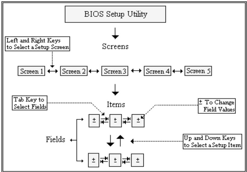
![The flowchart describes the navigation of a BIOS Setup Utility.\n\n**Top Section:**\n*   A top block labeled **'BIOS Setup Utility'** has an arrow pointing down to the text **'Screens'**.\n\n**Screen Navigation:**\n*   A block on the left labeled **'Left and Right Keys to Select a Setup Screen'** has a dotted arrow pointing down to a row of screens.\n*   The row contains five blocks connected by double-headed horizontal arrows: **'Screen 1'** (-) **'Screen 2'** (-) **'Screen 3'** (-) **'Screen 4'** (-) **'Screen 5'**.\n*   An arrow points down from the screen row to the text **'Items'**.\n\n**Field and Item Selection:**\n*   A block on the left labeled **'Tab Key to Select Fields'** has a dotted arrow pointing to the top row of boxes.\n*   Below 'Items' is a grid of six boxes containing the symbol **'±'**.\n    *   There is a top row of three boxes connected by double-headed horizontal arrows.\n    *   There is a bottom row of three boxes connected by double-headed horizontal arrows.\n*   Between the top and bottom rows of boxes, there is a downward arrow (↓) and an upward arrow (↑).\n*   To the left of these boxes, the text **'Fields'** has lines pointing to both the top and bottom rows of boxes.\n\n**Value Modification:**\n*   A block on the right labeled **'± To Change Field Values'** has a dotted arrow pointing to the top row of boxes.\n*   A block on the right labeled **'Up and Down Keys to Select a Setup Item'** has a dotted arrow pointing to the up and down arrows between the rows of boxes.](.cpci-3620-50m-15098-2010-11/865989ffcf3666f205f0b65ef1f2f10dcbf88ce7f31a6c91cc175be38f3306a6.jpg)

![The image displays a white document icon with a folded top-right corner and faint horizontal lines, overlaid with a large red checkmark.](.cpci-3620-50m-15098-2010-11/87132c8e074d3806f2691b1ca835a310402acfb43325463793152b999a848503.jpg)
NOTE:

There is a hot key legend located in the right frame on most setup screens.

→←

Left/Right. The Left and Right &lt; Arrow &gt; keys allow you to select a setup screen. For example: Main screen, Advanced screen, Chipset screen, and so on.

↑↓

Up/Down The Up and Down &lt; Arrow &gt; keys allow you to select a setup item or sub-screen.

+-

Plus/Minus The Plus and Minus &lt; Arrow &gt; keys allow you to change the field value of a particular setup item. For example: Date and Time.

Tab

The &lt; Tab &gt; key allows you to select setup fields.

ESC

The &lt; Esc &gt; key allows you to discard any changes you have made and exit the Setup. Press the &lt; Esc &gt; key to exit the setup without saving your changes. Press the &lt; Enter &gt; key to discard changes and exit. You can also use the &lt; Arrow &gt; key to select Cancel and then press the &lt; Enter &gt; key to abort this function and return to the previous screen.

# 8.2 Main Setup

When you first enter the Setup Utility, you will enter the Main setup screen. You can always return to the Main setup screen by selecting the Main tab. There are two Main Setup options. They are described in this section. The Main BIOS Setup screen is shown below.
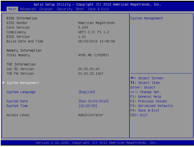
![Aptio Setup Utility - Copyright (C) 2013 American Megatrends, Inc.\nMain Advanced Chipset Security Boot Save & Exit\nBIOS Information\nBIOS Vendor American Megatrends\nCore Version 5.009\nCompliancy UEFI 2.3; PI 1.2\nBIOS Version 1.01\nBuild Date and Time 06/03/2014 14:48:58\nMemory Information\nTotal Memory 4096 MB (LPDDR3)\nTXE Information\nSec RC Version 00.05.00.00\nTXE FW Version 01.00.02.1067\nSystem Management\nSystem Language (English)\nSystem Date (Sun 01/01/2012)\nSystem Time (12:22:50)\nAccess Level Administrator\nSystem Management\n↑↓: Select Item\nEnter: Select\n+/-: Change Opt.\nF1: General Help\nF2: Previous Values\nF3: Optimized Defaults\nF4: Save & Exit\nESC: Exit\nVersion 2.16.1242. Copyright (C) 2013 American Megatrends, Inc.](.cpci-3620-50m-15098-2010-11/903d78ef07d2b3745abc4dcdfbecc0e8df702005db29354d6d113010601c8cac.jpg)

# Board Information

# BIOS Vendor

Display the BIOS vendor

# Core Version

Display the BIOS core version

# BIOS Version

Display the current BIOS revision

# Build Data and Time

Display the BIOS build data

# Memory Information

Display the system memory data.

# System Management
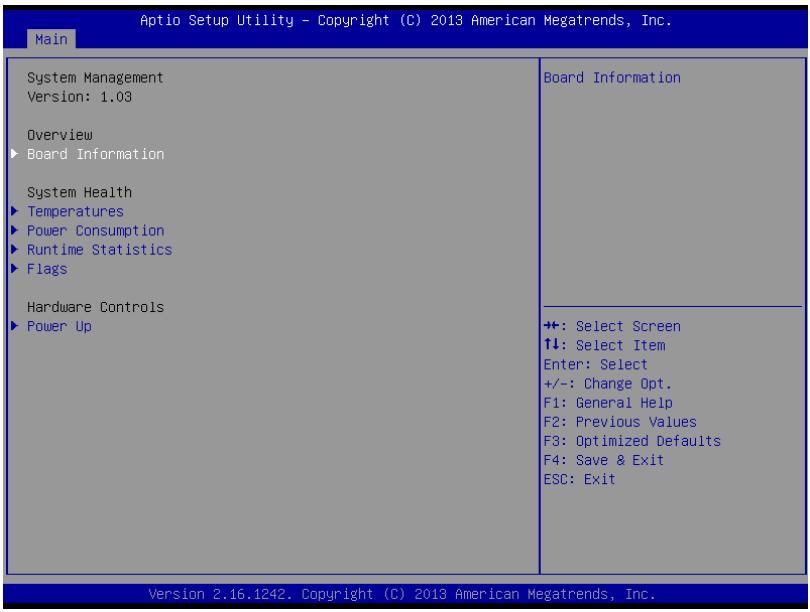
![Aptio Setup Utility - Copyright (C) 2013 American Megatrends, Inc.\nMain\nSystem Management\nVersion: 1.03\nOverview\n► Board Information\nSystem Health\n► Temperatures\n► Power Consumption\n► Runtime Statistics\n► Flags\nHardware Controls\n► Power Up\nBoard Information\n+: Select Screen\n↑↓: Select Item\nEnter: Select\n+/-: Change Opt.\nF1: General Help\nF2: Previous Values\nF3: Optimized Defaults\nF4: Save & Exit\nESC: Exit\nVersion 2.16.1242. Copyright (C) 2013 American Megatrends, Inc.](.cpci-3620-50m-15098-2010-11/404746a1119ad0dfdf42e7e00da8fe7ce66cad0e4f106d3c222b794684c522a1.jpg)

# Board Information

Display information from SEMA via the SMBus: SEMA Firmware, SEMA Bootloader, Build Date, Hardware Version, Serial Number, Manufacturing Date, Last Repair Date, MAC ID

# System Health

Displays CPU and Board Temperatures, Power Consumption, Runtime Statistics, BMC Flags.

# Power Up

Enable/Disable the Power-Up Watchdog.

<table><tr><td colspan="2">Aptio Setup Utility - Copyright (C) 2013 American Megatrends, Inc.</td></tr><tr><td>Power Up
Power-Up Watchdog [Disabled]
ATTENTION: Pressing *** during start up disables the Power Up Watchdog.</td><td>The Power Up Watchdog resets the system after a certain amount of time after power up.</td></tr></table>

# System Language

Choose the system default language.

# System Time/System Date

Use this option to change the system time and date. Highlight System Time or System Date using the &lt; Arrow &gt; keys. Enter new values using the keyboard. Press the &lt; Tab &gt; key or the &lt; Arrow &gt; keys to move between fields. The date must be entered in MM/DD/YY format. The time is entered in HH:MM:SS format.

![The image displays a white document icon with a folded top-right corner and faint gray horizontal lines, featuring a large, bold red checkmark superimposed over it.](.cpci-3620-50m-15098-2010-11/9c5816eb07d02d068292e77826b3560468bd1b8b699dd480be7262a8011cdba1.jpg)
NOTE:

The time is in 24-hour format. For example, 5:30 A.M. appears as 05:30:00, and 5:30 P.M. as 17:30:00.

# 8.3 Advanced BIOS Setup

Select the Advanced tab from the setup screen to enter the Advanced BIOS Setup screen. You can select any of the items in the left frame of the screen, such as SuperIO Configuration, to go to the sub menu for that item. You can display an Advanced BIOS Setup option by highlighting it using the &lt; Arrow &gt; keys. The Advanced BIOS Setup screen is shown below.

<table><tr><td colspan="2">Aptio Setup Utility - Copyright (C) 2013 American Megatrends, Inc.</td></tr><tr><td colspan="2">Main Advanced Chipset Security Boot Save &amp; Exit</td></tr><tr><td rowspan="2">IT8783F Super IO Configuration
► Serial Port Console Redirection
► CPU Configuration
► PPM Configuration
► Thermal Configuration
► IDE Configuration
► Network Stack Configuration
► CSM Configuration
► USB Configuration
► Intel(R) I210 Gigabit Network Connection - 00:0A:09:00:...
► Intel(R) I210 Gigabit Network Connection - 00:0A:09:00:...</td><td>System Super IO Chip Parameters.</td></tr><tr><td>+: Select Screen
↑↓: Select Item
Enter: Select
+/-: Change Opt.
F1: General Help
F2: Previous Values
F3: Optimized Defaults
F4: Save &amp; Exit
ESC: Exit</td></tr><tr><td colspan="2">Version 2.16.1242. Copyright (C) 2013 American Megatrends, Inc.</td></tr></table>

# 8.3.1 Super IO Configuration

You can use this screen to select options for the Super IO settings. Use the up and down &lt; Arrow &gt; keys to select an item. Use the &lt; + &gt; and &lt; - &gt; keys to change the value of the selected option. The settings are described on the following pages. The screen is shown below.
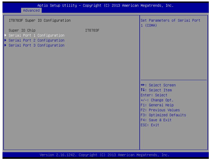
![Aptio Setup Utility - Copyright (C) 2013 American Megatrends, Inc.\nAdvanced\nIT8783F Super IO Configuration\nSuper IO Chip                    IT8783F\n► Serial Port 1 Configuration\n► Serial Port 2 Configuration\n► Serial Port 3 Configuration\nSet Parameters of Serial Port\n1 (COMA)\n+: Select Screen\n↑↓: Select Item\nEnter: Select\n+/-: Change Opt.\nF1: General Help\nF2: Previous Values\nF3: Optimized Defaults\nF4: Save & Exit\nESC: Exit\nVersion 2.16.1242. Copyright (C) 2013 American Megatrends, Inc.](.cpci-3620-50m-15098-2010-11/741fd45dccb3729fafcc04f0f5341b6616b649c7d055506effbc73072c34c1b4.jpg)

# Serial Port1-3 Configuration

<table><tr><td colspan="2">Aptio Setup Utility - Copyright (C) 2013 American Megatrends, Inc. Advanced</td></tr><tr><td>Serial Port 1 Configuration Serial Port [Enabled] Device Settings IO=3F8h; IRQ=4;</td><td>Enable or Disable Serial Port (COM)</td></tr></table>

This option enables/disables Serial Ports 1-3, which have fixed I/O port addresses and IRQs: Port1: IO=3F8, IRQ=4, Port2: IO=2F8, IRQ=3, Port3: IO=3E8, IRQ=5.

# 8.3.2 Serial Port Console Redirection

These settings specify how the host computer and the remote computer will exchange data. Both computers should have the same or compatible settings. The screen is shown below.

![Aptio Setup Utility - Copyright (C) 2013 American Megatrends, Inc.\nAdvanced\nCOM1\nConsole Redirection (Disabled)\n► Console Redirection Settings\nCOM2\nConsole Redirection (Disabled)\n► Console Redirection Settings\nCOM3\nConsole Redirection (Disabled)\n► Console Redirection Settings\nConsole Redirection Enable or\nDisable.\n+: Select Screen\n↑↓: Select Item\nEnter: Select\n+/-: Change Opt.\nF1: General Help\nF2: Previous Values\nF3: Optimized Defaults\nF4: Save & Exit\nESC: Exit\nVersion 2.16.1242. Copyright (C) 2013 American Megatrends, Inc.](.cpci-3620-50m-15098-2010-11/5062268d0b1f274d24bc630a85113767ec3bbb4646a7bcc25698d1997cb69ad4.jpg)

# COM1/COM2/COM3 Console Redirection

Enable or disable console redirection on COM1/2/3.

# COM1/2/3 Console Redirection Settings

<table><tr><td colspan="2">Aptio Setup Utility - Copyright (C) 2013 American Megatrends, Inc. Advanced</td></tr><tr><td>COM1Console Redirection SettingsTerminal Type [ANSI]Bits per second [115200]Data Bits [B]Parity [None]Stop Bits [I]Flow Control [None]VT-UTF8 Combo Key Support [Enabled]Recorder Mode [Disabled]Resolution 100x31 [Disabled]Legacy OS Redirection Resolution [80x24]Putty KeyPad [VT100]Redirection After BIOS POST [Always Enable]</td><td>Emulation: ANSI: ExtendedASCII char set. VT100: ASCIIchar set. VT100+: ExtendsVT100 to support color, function keys, etc. VT-UTF8: Uses UTF8 encoding to map Unicode chars onto 1 or more bytes.+: Select Screen↑↓: Select ItemEnter: Select+/-: Change Opt.F1: General HelpF2: Previous ValuesF3: Optimized DefaultsF4: Save &amp; ExitESC: Exit</td></tr><tr><td colspan="2">Version 2.16.1242. Copyright (C) 2013 American Megatrends, Inc.</td></tr></table>

# Terminal Type

VT100+ is the preferred terminal type for out-of-band management. Configuration options: VT100, VT100+, VT-UTF8, ANSI.

# Bits per Second

Select the bits per second you want the serial port to use for console redirection. The options are 115200, 57600, 38400, 19200, 9600.

# Data Bits

Select the data bits you want the serial port to use for console redirection. Set this value to 7, 8.

# Parity

Set this option to select Parity for console redirection. The settings for this value are None, Even, Odd, Mark, Space.

# Stop Bits

Stop bits indicate the end of a serial data packet. (A start bit indicates the beginning). The standard setting is 1 stop bit.

Communication with slow devices may require more than 1 stop bit. Set this value to 1 and 2.

# Flow Control

Set this option to select Flow Control for console redirection. The settings for this value are None, Hardware RTS/CTS.

# VT-UTF8 Combo Key Support

Enables VT-UTF8 combination key support for ANSI/VT100 terminals.Set this value to Enabled/Disabled.

# Recorder Mode

When this mode is enabled, only text will be sent. This is to capture terminal data. Set this value to Enabled/Disabled.

# Resolution 100x31

Set this option to extended terminal resolution. Set this value to Enabled/Disabled.

# Legacy OS Redirection

On legacy OS, the number of rows and columns supported for redirection. Set this value to 80x24, 80x25.

# Putty Key Pad

Select FunctionKey and KeyPad on Putty. Set this value to VT100, LINUX, XTERMR6, SCO, ESCN, VT400.

# Redirection After BIOS POST

Available options: 'Disabled', 'During Boot Loader' or 'Always'. If 'BootLoader' is selected, redirection is disabled before booting to legacy OS. The default value is 'Always Enable' which enables redirection for legacy OS.

# 8.3.3 CPU Configuration

You can use this screen to select options for the CPU Configuration Settings. Use the up and down &lt; Arrow &gt; keys to select an item. Use the &lt; + &gt; and &lt; - &gt; keys to change the value of the selected option. A description of the selected item appears on the right side of the screen. The settings are described on the following pages. An example of the CPU Configuration screen is shown below.

![Aptio Setup Utility - Copyright (C) 2013 American Megatrends, Inc.\nAdvanced\nCPU Configuration\n► Socket O CPU Information\nCPU Speed        1751 MHz\n64-bit         Supported\nActive Processor Cores    (All)\nSocket specific CPU Information\n+: Select Screen\n↑↓: Select Item\nEnter: Select\n+/-: Change Opt.\nF1: General Help\nF2: Previous Values\nF3: Optimized Defaults\nF4: Save & Exit\nESC: Exit\nVersion 2.16.1242. Copyright (C) 2013 American Megatrends, Inc.](.cpci-3620-50m-15098-2010-11/f0a1e78cd5578471c716e330a522821883f0750dece83737e65d4bd85c212533.jpg)

# Socket 0 CPU Information

This page displays CPU information, including and CPU signature, Microcode Patch, Max/Min CPU speed, Processor Cores, and Intel HT/Intel VT-x support.

<table><tr><td colspan="2">Aptio Setup Utility - Copyright (C) 2013 American Megatrends, Inc. Advanced</td></tr><tr><td>Socket O CPU Information</td><td></td></tr><tr><td>Intel(R) Atom(TM) CPU E3827 @ 1.74GHz</td><td></td></tr><tr><td>CPU Signature 30673</td><td></td></tr><tr><td>Microcode Patch 31e</td><td></td></tr><tr><td>Max CPU Speed 1740 MHz</td><td></td></tr><tr><td>Min CPU Speed 500 MHz</td><td></td></tr><tr><td>Processor Cores 2</td><td></td></tr><tr><td>Intel HT Technology Not Supported</td><td></td></tr><tr><td>Intel VT-x Technology Supported</td><td></td></tr><tr><td>L1 Data Cache 24 kB x 2</td><td></td></tr><tr><td>L1 Code Cache 32 kB x 2</td><td></td></tr><tr><td>L2 Cache 512 kB x 1</td><td></td></tr><tr><td>L3 Cache Not Present</td><td></td></tr><tr><td></td><td>+: Select Screen
↑↓: Select Item
Enter: Select
+/-: Change Opt.
F1: General Help
F2: Previous Values
F3: Optimized Defaults
F4: Save &amp; Exit
ESC: Exit</td></tr><tr><td colspan="2">Version 2.16.1242. Copyright (C) 2013 American Megatrends, Inc.</td></tr></table>

# Active Processor Core

Select the number of active CPU cores ("All" or "1").

# 8.3.4 PPM Configuration

![Aptio Setup Utility - Copyright (C) 2013 American Megatrends, Inc.\nAdvanced\nPPM Configuration\nEIST    (Enabled)\nEnable/Disable Intel SpeedStep\n+: Select Screen\n↑↓: Select Item\nEnter: Select\n+/-: Change Opt.\nF1: General Help\nF2: Previous Values\nF3: Optimized Defaults\nF4: Save & Exit\nESC: Exit\nVersion 2.16.1242. Copyright (C) 2013 American Megatrends, Inc.](.cpci-3620-50m-15098-2010-11/0cf6e572902bcf01c785ebed7c7e627cbfd1331c1e2f842f342b2cf6f6401364.jpg)

# EIST

Enhanced Intel SpeedStep® Technology allows the system to dynamically adjust processor voltage and core frequency, which can result in decreased average power consumption and decreased average heat production.

# 8.3.5 Thermal Configuration

<table><tr><td colspan="2">Aptio Setup Utility - Copyright (C) 2013 American Megatrends, Inc. Advanced</td></tr><tr><td rowspan="2">Thermal Configuration Parameters Critical Trip Point [Disabled] Passive Trip Point [Disabled]</td><td>This value controls the temperature of the ACPI critical Trip Point in which the OS will shut the system off.</td></tr><tr><td>+: Select Screen ↑↓: Select Item Enter: Select +/-: Change Opt. F1: General Help F2: Previous Values F3: Optimized Defaults F4: Save &amp; Exit ESC: Exit</td></tr><tr><td colspan="2">Version 2.16.1242. Copyright (C) 2013 American Megatrends, Inc.</td></tr></table>

# Critical Trip Poin

Sets the temperature of the ACPI critical trip point at which the OS will shut down.

# Passive Trip point

Sets the temperature of the ACPI passive trip point at which the OS will begin throttling the processor.

# 8.3.6 IDE Configuration

You can use this screen to select options for the IDE Configuration Settings. Use the up and down &lt; Arrow &gt; keys to select an item. Use the &lt; + &gt; and &lt; - &gt; keys to change the value of the selected option. A description of the selected item appears on the right side of the screen. The settings are described on the following pages.

<table><tr><td colspan="2">Aptio Setup Utility - Copyright (C) 2013 American Megatrends, Inc. Advanced</td></tr><tr><td colspan="2">IDE Configuration OS Selection [Windows 8.X] SATA Speed Support [Gen2] SATA Mode [AHCI Mode] Serial-ATA Port 0 [Enabled] Serial-ATA Port 1 [Enabled] SATA Port0 Not Present ++: Select Screen ↑↓: Select Item Enter: Select +/-: Change Opt. F1: General Help F2: Previous Values F3: Optimized Defaults F4: Save &amp; Exit ESC: Exit</td></tr><tr><td>SATA Port1 Not Present</td><td></td></tr></table>

# OS Selection

This item specifies support for Windows 8.x or Windows 7.

![The image displays a simple icon of a white document with a folded top-right corner and faint horizontal lines running across it. A large, bold red checkmark is superimposed over the center of the document.](.cpci-3620-50m-15098-2010-11/8937116912c78ee076507955383899b12c1ee73303f92330f36f494eba2bc1a1.jpg)
NOTE:

This item also sets CSM Configuration > Boot Option Filter / Storage / Video to UEFI only or Legacy only.

# SATA Speed Support

Set SATA supports to Gen1 or Gen2.

# SATA Mode

Select IDE or AHCI mode.

# Serial-ATA Port 0

Enable/Disable Serial ATA Port 0

# Serial-ATA Port 1

Enable/Disable Serial ATA Port 1

# 8.3.7 Network Stack Configuration

![Aptio Setup Utility - Copyright (C) 2013 American Megatrends, Inc.\nAdvanced\nNetwork Stack (Disabled) Enable/Disable UEFI Network Stack\n+: Select Screen\n↑↓: Select Item\nEnter: Select\n+/-: Change Opt.\nF1: General Help\nF2: Previous Values\nF3: Optimized Defaults\nF4: Save & Exit\nESC: Exit\nVersion 2.16.1242. Copyright (C) 2013 American Megatrends, Inc.](.cpci-3620-50m-15098-2010-11/173e8a2e6509a870562ac35256b84a209859df2be2efc5d5deeeedcd670bb390.jpg)

# Network stack

Enable/Disable the UEFI network stack.

<table><tr><td colspan="2">Aptio Setup Utility - Copyright (C) 2013 American Megatrends, Inc.</td></tr><tr><td>Advanced</td><td></td></tr><tr><td>Network Stack</td><td>[Enabled] Enable/Disable UEFI Network Stack</td></tr><tr><td>IPv4 PXE Support</td><td>[Enabled]</td></tr><tr><td>IPv6 PXE Support</td><td>[Disabled]</td></tr></table>

# IPv4 PXE Support

Enable/Disable IPv4 PXE Boot Support.

# IPv6 PXE Support

Enable/Disable IPv6 PXE Boot Support.

# 8.3.8 CSM Configuration

You can use this screen to select options for the Compatibility Support Module (CSM) settings. Use the up and down &lt; Arrow &gt; keys to select an item. Use the &lt; + &gt; and &lt; - &gt; keys to change the value of the selected option.

<table><tr><td colspan="2">Aptio Setup Utility - Copyright (C) 2013 American Megatrends, Inc. Advanced</td></tr><tr><td>Compatibility Support Module Configuration</td><td>Enable/Disable CSM Support.</td></tr><tr><td>CSM Support [Enabled]</td><td></td></tr><tr><td>Boot option filter [UEFI only]</td><td></td></tr><tr><td>Option ROM execution order</td><td></td></tr><tr><td>Network [Do not launch]</td><td></td></tr><tr><td>Storage [UEFI only]</td><td></td></tr><tr><td>Video [UEFI only]</td><td></td></tr><tr><td>Other PCI devices [Legacy only]</td><td></td></tr></table>

# CSM Support

Enable/Disable CSM Support

# Boot Option Filter

This option controls Legacy/UEFI ROM priority.

# Network

Setting "OS\_Select" to Windows 7 only supports PXE ROM boot. Setting "OS\_Select" to Window 8 only supports EFI Network Stack

# Storage

The Storage status is set by IDE Configuration > OS selection.

#

The Video status is set by IDE Configuration > OS Selection.

# Other PCI devices

Determines OpROM execution policy for devices other than Network, Storage, or Video.

# 8.3.9 USB Configuration

You can use this screen to select options for the USB Configuration. Use the up and down &lt; Arrow &gt; keys to select an item. The screen is shown below.

![Aptio Setup Utility - Copyright (C) 2013 American Megatrends, Inc.\nAdvanced\nUSB Configuration\nLegacy USB Support (Enabled)\nUSB Mass Storage Driver Support (Enabled)\nEnables Legacy USB support.\nAUTO option disables legacy\nsupport if no USB devices are\nconnected. DISABLE option will\nkeep USB devices available\nonly for EFI applications.\n+: Select Screen\n↑↓: Select Item\nEnter: Select\n+/-: Change Opt.\nF1: General Help\nF2: Previous Values\nF3: Optimized Defaults\nF4: Save & Exit\nESC: Exit\nVersion 2.16.1242. Copyright (C) 2013 American Megatrends, Inc.](.cpci-3620-50m-15098-2010-11/25cb36c44ce97e3661b666be532f797c9cfabf95a7002c847ba18ad3f60a6624.jpg)

# Legacy USB Support

Enables legacy USB support. Auto option disables legacy support if no USB devices are connected. Disable option will keep USB devices available only for EFI applications. Set this value to Enabled/Disabled/Auto.

# USB Mass Storage Driver Support

Enable/Disable USB mass storage driver support

# 8.4 Chipset Configuration

Select the Chipset tab from the setup screen to enter the Chipset BIOS Setup screen. You can select any of Chipset BIOS Setup options by highlighting it using the &lt; Arrow &gt; keys. The Chipset BIOS Setup screen is shown below.

![Aptio Setup Utility - Copyright (C) 2013 American Megatrends, Inc.\nMain Advanced Chipset Security Boot Save & Exit\nNorth Bridge\nSouth Bridge\nNorth Bridge Parameters](.cpci-3620-50m-15098-2010-11/a65b6ea16df359b14e44cafe9a230c9d2d21372f56bffe6e5e8e04efcbe4b08e.jpg)

# 8.4.1 North Bridge

<table><tr><td colspan="2">Aptio Setup Utility - Copyright (C) 2013 American Megatrends, Inc. Chipset</td></tr><tr><td>Intel IGD Configuration Memory Information Total Memory 4096 MB (LPDDR3) Memory Slot0 4096 MB (LPDDR3) Max TOLUD [Dynamic]</td><td>Config Intel IGD Settings.</td></tr></table>

# Memory Information

Displays the memory information.

# Max ToLUD

Select IGD dynamic or fixed mmio size

# Intel IGD Configuration

<table><tr><td colspan="2">Chipset</td></tr><tr><td>Intel IGD ConfigurationIntegrated Graphics Device [Enabled]Primary Display [IGD]DVMT Pre-Allocated [64M]</td><td>Enable : Enable Integrated Graphics Device (IGD) when selected as the Primary Video Adaptor. Disable: Always disbale IGD</td></tr></table>

# Integrated Graphics Device

Enabled: Integrated Graphics Device (IGD) when selected as the primary graphics adapter. Disable: Always disable IGD

# Primary Display

Select which graphics device (IGD/PCI) should be primary display

# DVMT Pre-Allocated

Select DVMT Pre-Allocated (fixed) graphics memory size used by the internal graphics device.

# 8.4.2 South Bridge

<table><tr><td colspan="2">Aptio Setup Utility - Copyright (C) 2013 American Megatrends, Inc.
Chipset</td></tr><tr><td>USB Configuration
PCI Express Configuration
VGA switch [Front]
LAN switch [Front]
SATA switch [Front]</td><td>USB Configuration Settings</td></tr><tr><td></td><td>+: Select Screen
↑↓: Select Item
Enter: Select
+/-: Change Opt.
F1: General Help
F2: Previous Values
F3: Optimized Defaults
F4: Save &amp; Exit
ESC: Exit</td></tr><tr><td colspan="2">Version 2.16.1242. Copyright (C) 2013 American Megatrends, Inc.</td></tr></table>

# VGA Switch

Sets the VGA output to the faceplate or to rear IO.

# LAN Switch

Sets the LAN1/2 output to the faceplate or to rear IO.

# SATA Switch

Sets the SATA1 output to the front blade or to rear IO.

# USB Configuration

<table><tr><td colspan="2">Aptio Setup Utility - Copyright (C) 2013 American Megatrends, Inc. Chipset</td></tr><tr><td>USB Configuration XHCI Mode [Enabled] USB 2.0(EHCI) Support [Disabled]</td><td>Mode of operation of xHCI controller</td></tr></table>

# XHCI Mode

# USB2.0 (EHCI)Support

The Intel “Bay Trail” platform only supports one XHCI/EHCI controller. If the OS selection is Windows 8, XHCI Mode must be enabled and USB 2.0 (EHCI) must be disabled. If the OS selection is Windows 7, USB 2.0 (EHCI) must be enabled and XHCI Mode must be disabled.

# PCI Express Configuration

<table><tr><td colspan="2">Aptio Setup Utility - Copyright (C) 2013 American Megatrends, Inc. Chipset</td></tr><tr><td>PCI Express ConfigurationPCI Express Port 0 [Enabled]Speed [Auto]PCI Express Port 1 [Enabled]Speed [Auto]PCI Express Port 2 [Enabled]Speed [Auto]PCI Express Port 3 [Enabled]Speed [Auto]</td><td>Enable or Disable the PCIExpress Port 0 in the Chipset.</td></tr></table>

# PCI Express Port 0/1/2/3

Enable/Disable PCI Express Port 0/1/2/3 on the chipset.

# Speed

Configure the PCIe Port Speed.

# 8.5 Security

<table><tr><td colspan="2">Aptio Setup Utility - Copyright (C) 2013 American Megatrends, Inc.</td></tr><tr><td>Password Description
If ONLY the Administrator&#x27;s password is set, then this only limits access to Setup and is only asked for when entering Setup.
If ONLY the User&#x27;s password is set, then this is a power on password and must be entered to boot or enter Setup. In Setup the User will have Administrator rights.
The password length must be in the following range:
Minimum length 3
Maximum length 20
Administrator Password
User Password</td><td>Set Administrator Password
+: Select Screen
↑↓: Select Item
Enter: Select
+/-: Change Opt.
F1: General Help
F2: Previous Values
F3: Optimized Defaults
F4: Save &amp; Exit
ESC: Exit</td></tr><tr><td colspan="2">Version 2.16.1242. Copyright (C) 2013 American Megatrends, Inc. 84</td></tr></table>

# Administrator, User Password

If only the administrator's password is set, then this only limits access to setup and is only asked for when entering setup.

If only the user's password is set, then this is a power on password and must be entered to boot or enter setup. In setup the user will have administrator rights.

# 8.6 Boot Settings

Select the Boot tab from the setup screen to enter the Boot BIOS Setup screen. You can select any of the items in the left frame of the screen and display a Boot BIOS Setup option by highlighting it using the &lt; Arrow &gt; keys. The Boot Settings screen is shown below:

<table><tr><td colspan="2">Aptio Setup Utility - Copyright (C) 2013 American Megatrends, Inc.</td></tr><tr><td colspan="2">Main Advanced Chipset Security Boot Save &amp; Exit</td></tr><tr><td>Boot Configuration
Setup Prompt Timeout 1
Bootup NumLock State [On]</td><td rowspan="3">Number of seconds to wait for setup activation key.
65535(0xFFFF) means indefinite waiting.</td></tr><tr><td>Quiet Boot [Disabled]</td></tr><tr><td>Boot Option Priorities
Boot Option #1 [Windows Boot Manage...]
Boot Option #2 [UEFI: Generic Flash...]
Boot Option #3 [UEFI: Built-in EFI ...]</td></tr></table>

# Setup Prompt Timeout

Number of seconds to wait for the setup activation key. 65535 (0xFFFF) means indefinite waiting.

# Bootup NumLock State

Select the keyboard NumLock state

# Quiet Boot

Disabled - Set this value to allow the computer system to display the POST messages.
Enabled - Set this value to allow the computer system to display the OEM logo.

# Boot Option Priorities

Set Boot Option #1-#3 boot priority.

# 8.7 Save & Exit Menu

Select the Save & Exit tab from the setup screen to enter the Save & Exit BIOS Setup screen. You can display an Exit BIOS Setup option by highlighting it using the &lt; Arrow &gt; keys. The Save & Exit BIOS Setup screen is shown below.

<table><tr><td colspan="2">Aptio Setup Utility - Copyright (C) 2013 American Megatrends, Inc.</td></tr><tr><td colspan="2">Main Advanced Chipset Security Boot Save &amp; Exit</td></tr><tr><td>Save Changes and Exit
Discard Changes and Exit
Save Changes and Reset
Discard Changes and Reset
Save Options
Save Changes
Discard Changes
Restore Defaults
Save as User Defaults
Restore User Defaults
Boot Override
Windows Boot Manager (P0: ASD26-HA2032-ET)
UEFI: Built-in EFI Shell
UEFI: Generic Flash Disk 5.00</td><td>Exit system setup after saving the changes.
+: Select Screen
↑↓: Select Item
Enter: Select
+/-: Change Opt.
F1: General Help
F2: Previous Values
F3: Optimized Defaults
F4: Save &amp; Exit
ESC: Exit</td></tr><tr><td colspan="2">Version 2.16.1242. Copyright (C) 2013 American Megatrends, Inc.</td></tr></table>

# Save Changes and Exit/Reset

When you have completed the system configuration changes, select this option to leave setup / reboot the computer so the new system configuration parameters can take effect.

# Discard Changes and Exit/Reset

Select this option to leave setup / reboot the computer without making any permanent changes to the system configuration.

# Save Changes

Save Changes done so far to any of the setup options.

# Discard Changes

Select Discard Changes from the Exit menu and press &lt; Enter &gt;.

Select Ok to discard changes.

# Restore Defaults

Automatically sets all Setup options to a complete set of default settings when you select this option. The Optimal settings are designed for maximum system performance, but may not work best for all computer applications. In particular, do not use the Optimal Setup options if your computer is experiencing system configuration problems.

# Save as User Defaults

Save the changes done so far as User Defaults.

# Restore User Defaults

Restore the User Defaults to all the setup options.

This page intentionally left blank.

# Important Safety Instructions

For user safety, please read and follow all instructions, WARNINGS, CAUTIONS, and NOTES marked in this manual and on the associated equipment before handling/operating the equipment.

X Read these safety instructions carefully.
X Keep this user’s manual for future reference.
? Read the specifications section of this manual for detailed information on the operating environment of this equipment.
X When installing/mounting or uninstalling/removing equipment:

Z Turn off power and unplug any power cords/cables.

X To avoid electrical shock and/or damage to equipment:

Z Keep equipment away from water or liquid sources;
Z Keep equipment away from high heat or high humidity;
Z Keep equipment properly ventilated (do not block or cover ventilation openings);

Z Make sure to use recommended voltage and power source settings;

Z Always install and operate equipment near an easily accessible electrical socket-outlet;

Z Secure the power cord (do not place any object on/over the power cord);

Z Only install/attach and operate equipment on stable surfaces and/or recommended mountings; and,

Z If the equipment will not be used for long periods of time, turn off and unplug the equipment from its power source.

X Never attempt to fix the equipment. Equipment should only be serviced by qualified personnel.

A Lithium-type battery may be provided for uninterrupted, backup or emergency power.

![The image displays a standard warning sign. It features a red triangle with a white exclamation point centered inside. Below the triangle, the text 'WARNING:' appears in black capital letters.](.cpci-3620-50m-15098-2010-11/833e7519ff78bf6ed6b3cf39f58fecc761f13768bee64102f311f3c0e8b3f845.jpg)

Risk of explosion if battery is replaced with one of an incorrect type. Dispose of used batteries appropriately.

X Equipment must be serviced by authorized technicians when:

Z The power cord or plug is damaged;
Z Liquid has penetrated the equipment;
Z It has been exposed to high humidity/moisture;
Z It is not functioning or does not function according to the user’s manual;
Z It has been dropped and/or damaged; and/or,
Z It has an obvious sign of breakage.

# Getting Service

Ask an Expert: https://www.adlinktech.com/en/Askanexpert

# ADLINK Technology, Inc.

No. 66, Huaya 1st Road, Guishan District

Taoyuan City 333, Taiwan

Tel: +886-3-216-5088

Fax: +886-3-328-5723

Email: service@adlinktech.com

# Ampro ADLINK Technology, Inc.

6450 Via Del Oro, San Jose,

CA 95119-1208, USA

Tel: +1-408-360-0200

Toll Free: +1-800-966-5200 (USA only)

Fax: +1-408-600-1189

Email: info@adlinktech.com

# ADLINK Technology (China) Co., Ltd.

300 Fang Chun Rd., Zhangjiang Hi-Tech Park

Pudong New Area, Shanghai, 201203 China

Tel: +86-21-5132-8988

Fax: +86-21-5132-3588

Email: market@adlinktech.com

# ADLINK Technology GmbH

Hans-Thoma-Straße 8-10

D-68163 Mannheim, Germany

Tel: +49-621-43214-0

Fax: +49-621 43214-30

Email: emea@adlinktech.com

Please visit the Contact page at www.adlinktech.com for information on how to contact the ADLINK regional office nearest you.
[🔗 Link to the original document](.cpci-3620-50m-15098-2010-11/cpci-3620-50m-15098-2010-11.pdf)
