# cPCI-6636 Series

Value 6U CompactPCI®

Intel® Xeon® E3, Core™ i7/i3 Processor Blade

# User's Manual

![Back view of a green printed circuit board with various electronic components and connectors (no visible text or symbols)](.cpci-6636-50-15111-2000-01-preliminary/908dfe2dbe8e55af45460edc7bb017a5a46c89e0e64ea0c1d4b9f2350172bbe4.jpg)

![Back view of a computer motherboard with visible ports and connectors (no text or symbols)](.cpci-6636-50-15111-2000-01-preliminary/1ff0a1f283a026950d4f39c29a82bd28f06ccf7de78564962271e99d0dbacd07.jpg)

![Close-up of a green printed circuit board with multiple ports and connectors (no visible text or symbols)](.cpci-6636-50-15111-2000-01-preliminary/a946619b6103fbc9fa3b71dc43dbe245b5db9b3983326046081d2b5425055cf9.jpg)

Manual Rev.: 0.1

Revision Date: August 20, 2018

Part No: 50-15111-2000

# Revision History

<table><tr><td>Revision</td><td>Release Date</td><td>Description of Change(s)</td></tr><tr><td>0.1</td><td>2018-08-20</td><td>Preliminary release</td></tr></table>

# Preface

# Copyright 2018 ADLINK Technology Inc.

This document contains proprietary information protected by copyright. All rights are reserved. No part of this manual may be reproduced by any mechanical, electronic, or other means in any form without prior written permission of the manufacturer.

# Disclaimer

The information in this document is subject to change without prior notice in order to improve reliability, design, and function and does not represent a commitment on the part of the manufacturer.

In no event will the manufacturer be liable for direct, indirect, special, incidental, or consequential damages arising out of the use or inability to use the product or documentation, even if advised of the possibility of such damages.

# Environmental Responsibility

ADLINK is committed to fulfill its social responsibility to global environmental preservation through compliance with the European Union's Restriction of Hazardous Substances (RoHS) directive and Waste Electrical and Electronic Equipment (WEEE) directive. Environmental protection is a top priority for ADLINK. We have enforced measures to ensure that our products, manufacturing processes, components, and raw materials have as little impact on the environment as possible. When products are at their end of life, our customers are encouraged to dispose of them in accordance with the product disposal and/or recovery programs prescribed by their nation or company.

![Symbol of a trash bin crossed with a diagonal line and a horizontal bar below (no text or labels)](.cpci-6636-50-15111-2000-01-preliminary/463d302e70a71220d3abc75cfaa6020e8e095514fd13c3ec4fb37b941c769724.jpg)

Battery Labels (for products with battery)

![Symbol of a trash bin crossed out by two diagonal lines (no text or labels)](.cpci-6636-50-15111-2000-01-preliminary/c0f77f6e0cbffd06fc247a30b0e95b7b8682103656942b7b6c1a484df1322d9e.jpg)

![Simple recycling symbol icon with three chasing arrows inside a square border (no text or labels)](.cpci-6636-50-15111-2000-01-preliminary/d8a79c8214177542caf8f744c549b2de6b7491f963b327fcabfa6a200943ceb0.jpg)

Li-ion

![RECYCLE\nRBRC\nLi-ion\n7.800.822.8837](.cpci-6636-50-15111-2000-01-preliminary/6c4c6dd03a929f1e93280132854fe172cdceee6027214fc6364a3d438a38dcc7.jpg)

![Abstract geometric pattern with interlocking black and white shapes (no text or symbols)](.cpci-6636-50-15111-2000-01-preliminary/f9a275e0cbabd21585297b1ecd205fca629232816acfb2eadedb1444b5debd0c.jpg)

廢電池請回收

# California Proposition 65 Warning

![A yellow triangular warning sign with a thick black border containing a black exclamation point in the center.](.cpci-6636-50-15111-2000-01-preliminary/857e2c28beca75ca9850a300e0f0bbea7d6f85c9fc55c840c040286314e53729.jpg)

WARNING: This product can expose you to chemicals including acrylamide, arsenic, benzene, cadmium, Tris(1,3-dichloro-2-propyl)phosphate (TDCPP), 1,4-Dioxane, formaldehyde, lead, DEHP, styrene, DINP, BBP, PVC, and vinyl materials, which are known to the State of California to cause cancer, and acrylamide, benzene, cadmium, lead, mercury, phthalates, toluene, DEHP, DIDP, DnHP, DBP, BBP, PVC, and vinyl materials, which are known to the State of California to cause birth defects or other reproductive harm. For more information go to www.P65Warnings.ca.gov.

# Trademarks

Product names mentioned herein are used for identification purposes only and may be trademarks and/or registered trademarks of their respective companies.

# Conventions

Take note of the following conventions used throughout this manual to make sure that users perform certain tasks and instructions properly.

![The image displays a white document icon with a folded upper-right corner and horizontal lines across the page. A large red checkmark is superimposed over the document. There is no text.](.cpci-6636-50-15111-2000-01-preliminary/f262969635fa7a1ca5d8562d12eaf3ed196c6460a5a571f6ca1c26eb481211bb.jpg)
NOTE:

Additional information, aids, and tips that help users perform tasks.

![The image shows a yellow triangular warning sign with a thick black border. Centered within the triangle is a large black exclamation point. The sign is positioned against a white background.](.cpci-6636-50-15111-2000-01-preliminary/500c2dddfb093d090bf8d808b6e341af9c1d91cd87dfc602ad967a0d1eb61d24.jpg)
CAUTION:

Information to prevent minor physical injury, component damage, data loss, and/or program corruption when trying to complete a task.

![A red triangular warning sign with a white exclamation mark in the center.](.cpci-6636-50-15111-2000-01-preliminary/2798907402eea421c31f934b8ef99ff44e24fe535660ad3c0f032402921853ce.jpg)
WARNING:

Information to prevent serious physical injury, component damage, data loss, and/or program corruption when trying to complete a specific task.

# Table of Contents

# Revision History...... ii

# Preface...... iii

# List of Figures ...... vii

# List of Tables ix

# 1 Introduction ...... 1

1.1 Overview.... 1
1.2 Features.... 2
1.3 Model Number Decoder 4
1.4 Package Contents 5

# 2 Specifications.... 7

2.1 cPCI-6636(D) Processor Blade Specifications 7
2.2 Block Diagrams.... 10
2.3 I/O Connectivity Table 11
2.4 Power Requirements 12

# 3 Functional Description 13

3.1 Processors.... 13
3.2 Chipset.... 16
3.3 XMC 17
3.4 Intel® Turbo Boost Technology 17
3.5 Intel® Hyper-Threading Technology 18
3.6 Battery 18

# 4 Board Interfaces.... 19

4.1 cPCI-6636(D) Component Side Layout 19
4.2 cPCI-6636D/DZ Assembly Layoutt 20

4.3 cPCI-6636(D/DZ) Faceplate I/O 21
4.4 Connector Pin Assignments.... 23
4.5 Switches and Buttons 35

# Important Safety Instructions.... 41

# Getting Service 43

# List of Figures

Figure 2-1: cPCI-6636(D/DZ) Blade Functional Block Diagram..... 10
Figure 4-1: cPCI-6636(D) Component Side Layout .... 19
Figure 4-2: cPCI-6636D/DZ Assembly Layout....20
Figure 4-3: cPCI-6636(D/DZ) Faceplate I/O 21
Figure 4-4: cPCI-6636 Series Switch Locations - Component Side. 35
Figure 4-5: cPCI-6636 Series Switch Locations - Solder Side...... 36

This page intentionally left blank.

# List of Tables

Table 2-1: cPCI-6636 Processor Blade Specifications .... 7

Table 2-2: cPCI-6636(D/DZ) I/O Connectivity....11

Table 4-1: cPCI-6636(D) Front Panel System LED Descriptions ... 22

Table 4-2: LAN1/2 RJ-45 GbE Pin Definitions 23

Table 4-3: LAN LED Status Definitions....23

Table 4-4: USB 3.0 Pin Definitions 24

Table 4-5: cPCI-6636(D) COM Pin Definitions ....24

Table 4-6: cPCI-6636(D) COM RJ-45 to DB-9 Cable Pin Definitions25

Table 4-7: cPCI-6636DZ COM1/2 Pin Definitions....25

Table 4-8: cPCI-6636DZ COM3/4 Pin Definitions....26

Table 4-9: cPCI-6636DZ COM5/6 Pin Definitions....26

Table 4-10: cPCI-6636DZ COM RJ-45 to 2x DB-9 Cable Pin Definitions 27

Table 4-11: DVI-I Connector Pin Definition....28

Table 4-12: Serial ATA 7-pin Connector Pin Definition....29

Table 4-13: Serial ATA Connector with power Pin Definition......29

Table 4-14: CFast Socket Pin Definition....30

Table 4-15: CompactPCI J1 Connector Pin Definition....31

Table 4-16: CompactPCI J2 Connector Pin Definition....32

Table 4-17: CompactPCI J3 Connector Pin Definition.... 33

Table 4-18: CompactPCI J5 Connector Pin Definition....34

This page intentionally left blank.

# 1 Introduction

# 1.1 Overview

The ADLINK cPCI-6636 Series is a 6U CompactPCI® processor blade based on the Intel® Xeon® E3 and 6th Generation Intel® Core™ i7/i3 Processors with Intel® HM170 or CM236 Chipsets. When paired with the Intel® CM236, the cPCI-6636 supports ECC memory. The cPCI-6636 supports up to 16GB onboard DDR4-2133 memory and 16GB DDR4-2133 via SODIMM. Total memory capacity is up to 32GB of DDR4-2133. The cPCI-6636 is a highly integrated processor blade fit for mission critical applications in industries ranging from automation to defence.

The cPCI-6636 Series supports flexible I/O interfaces with the cPCI-6636 in single-slot (4HP) and cPCI-6636D/DZ in dual slot (8HP) width form factors. Faceplate I/O for the cPCI-6636 (4HP) includes 2x GbE supported by an Intel® i219LM PHY controller and Intel® i210IT Ethernet controller, 3x USB 3.0, 1x RJ-45 serial port, and 1x DVI-I. Onboard I/O includes one 2.5" SATA drive space, one 7-pin SATA connector, and one CFast slot by adapter board. The cPCI-6636D (8HP) has identical I/O to the single-slot version, except that an XMC connector via PCIe x8 adapter board is supported in place of the CFast slot. A third configuration, the cPCI-6636DZ, supports 8x USB 3.0, 2x GbE, 6x serial TX/RX and 2x VGA on the faceplate, and the same onboard I/O as the two-slot "D" version. The cPCI-6636 Series supports with 66/64-bit PCI signaling. Additional signals including additional 3x SATA, up to 4x Ethernet ports, USB 2.0, PCIe x4, audio, display, and serial signals to rear J3 and J5 (DZ version supports no rear I/O). Graphics support is integrated on the Intel® processor with VGA and DVI-I options. Rear display output signal is reserved to J3 and J5 as option.

Rear I/O signals are available on cPCI-6636 and cPCI-6636D which are equipped with CompactPCI J3 and J5 connectors. Available to the RTM are up to 2x GbE to J3 by Intel® I210IT Ethernet controllers for PICMG 2.16, and an additional 2x GbE switchable to rear from the front panel for a total of up to 4x Ethernet to rear J3 and J5. Also available are 1x VGA to J3, 1x TMDS to J5, 2x SATA 1.5 Gb/s to J3, 1x SATA 1.5 Gb/s to J5, 6x USB 2.0 to

J3, 10x GPIO to J3 and J5, HDA and KB/MS to J3, and serial ports to J5. For PCIe expansion, the cPCI-6636 offers one PCIe x4 or 4x PCIe x1 to J5.

The ADLINK 8HP cPCI-6636DZ only supports operation in host slots, whereas the cPCI-6636 and cPCI-6636D operate independently in both host and peripheral slots without CompactPCI bus communication (satellite mode), making it ideal for high density computing platforms. Moreover, the cPCI-6636 supports remote manageability by SEMA for system health monitoring over the Internet.

The cPCI-6636 Series offers outstanding computing power from the latest Intel® processors and is an ideal solution for military, automation and other robust computing applications that require the highest computing power in a rugged, reliable CompactPCI system.

# 1.2 Features

▶ 6U CompactPCI blade in 4/8HP width form factor
▶ 14nm uFC-BGA Intel® Processor
Intel® Xeon® E3-1505M v5, 2.8/3.7GHz, 4C/8T, GT2, 8M, 45W (35W by cTDP)
Intel® Core™ i7-6820EQ 2.8/3.5GHz, 4C/8T, GT2, 8M, 45W
Intel® Core™ i3-6100E 2.7GHz, 2C/4T, GT2, 3M, 35W

▶ One channel DDR4-2133 soldered SDRAM with ECC up to 16GB; one channel with one socket SO-DIMM DDR4-2133 ECC memory up to 16GB (ECC is supported by default on cPCI-6636 and cPCI-6636D, Core™ i7 SKUs do not support ECC)

▶ Supports up to two independent displays
▶ cPCI-6636, cPCI-6636D support one DVI-I on front panel, additional 2x DVI routed to J3 and J5
▶ cPCI-6636DZ support 2x VGA on front panel, no rear I/O graphics
▶ 64-bit/66MHz CompactPCI interface based on PCI specifications, universal V(I/O)
▶ cPCI-6636DZ supports operation in host slot only

▶ cPCI-6636, cPCI-6636D support satellite mode operation in host and peripheral slots
▶ One PCIe x8 Gen3 XMC site on cPCI-6636D and cPCI-6636DZ
▶ Supports SEMA for system health monitoring
▶ 2x Gigabit Ethernet egress ports on faceplate provided by an Intel® I219LM and I210IT GbE controller via PCIe x1 and two additional Gigabit Ethernet ports Intel® I210IT routed to J3 (PICMG 2.16 compliant); all four GbE can be routed to rear
▶ 1x 2.5" SATA drive space and one 7-pin SATA on all cPCI-6636 Series
▶ 1x CFast slot on cPCI-6636 single-slot version
▶ 1x XMC slot on cPCI-6636D and cPCI-6636DZ
▶ 2x SATA 1.5 Gb/s to J3, 1x SATA 1.5 Gb/s to J5
▶ 6x USB 2.0, HDA, KB/MS, RS-232 to J3
RS-232 TX/RX to J5
▶ 10x GPIO to J3 and J5
TPM 2.0 support (Infineon SLB 9665XT2.0), not supported by cPCI-6636DZ

# 1.3 Model Number Decoder

$$
\mathrm{cPCI-ET6636SLXX/6820E/MX-X/X}
$$

(A)

(B)

(C)

(D)(E)(F)

(A) Operating Temperature Code

$$
\text { Blank } = 0 ^ {\circ} \mathrm{C} \text {   to   } + 6 0 ^ {\circ} \mathrm{C}
$$

$$
\mathbf {E T} = - 2 0 ^ {\circ} \mathrm{C} \text {   to   } + 7 0 ^ {\circ} \mathrm{C} (\text { for   CPUs   with   TDP   below   37W   only })
$$

(B) Configuration Code

Blank = cPCI-6636 single slot with I/O (DVI-I, COM, USB 3.0 x3, GbE x2), CFast slot, and J3/J5

D = cPCI-6636D dual slot with I/O (DVI-I, COM, USB 3.0 x3, GbE x2), XMC slot, and J3/J5

DZ = cPCI-6636DZ dual slot with I/O (VGA x2, COM x6, USB 3.0 x8, GbE x2) and XMC slot, without J3/J5

(C) CPU Code

$$
1 5 0 5 \mathrm{Mv} 5 = \text { Xeon } ^ {\circledR} \text { E3 - 1505M   v5 }
$$

$$
6 8 2 0 E = \text { Core } ^ {\text { TM }} \text {   i7   } 6 8 2 0 E Q
$$

$$
\mathbf {6 1 0 0 E} = \text { Core } ^ {\text { TM }} \text {   i3   } 6 1 0 0 \text { E }
$$

(D) Onboard Memory Capacity Code

$$
\mathbf {M 4} = 4 \mathrm{GB} \text { onboard   memory }
$$

$$
\mathbf {M 8} = 8 \mathrm{GB} \text { onboard   memory }
$$

$$
\mathbf {M 1 6} = 1 6 \mathrm{GB} \text { onboard   memory }
$$

(E) SODIMM Memory Capacity Code

$$
4 = 4 \mathrm{GB} \text { SODIMM }
$$

$$
\mathbf {8} = 8 \mathrm{GBSODIMM}
$$

$$
1 6 = 1 6 \mathrm{GB} \text { SODIMM }
$$

(F) Other information

# 1.4 Package Contents

The cPCI-6636 is packaged with the following components. If any of the following items are missing or damaged, retain the shipping carton and packing material and contact the dealer for inspection. Please obtain authorization before returning any product to ADLINK. The packing contents of cPCI-6636 Series non-standard configurations will vary depending on customer requests.

# cPCI-6636(D) Processor Blade

▶ Processor Blade
▷ CPU and memory specifications will differ depending on options selected
▷ Thermal module is assembled on the board
▶ RJ-45 to DB-9 COM adapter cable (PN: 30-01020-0200)
▶ 2.5" SATA drive accessory pack (PN: 58-99097-0010)
▶ 2.5" SATA adapter board (PN: 59-37571-0000)
▶ CFast accessory pack (PN: 58-99300-0000, cPCI-6636 only)
▶ DB-CFAST adapter board (PN: 59-37572-0000, cPCI-6636 only)

# cPCI-6636DZ Processor Blade

▶ Processor Blade
▷ CPU and memory specifications will differ depending on options selected
▶ Thermal module is assembled on the board

▶ 2x RJ-45 to DB-9 COM adapter cable (PN: 30-25044-1020)

▶ 2.5" SATA drive accessory pack (PN: 58-99097-0010)

▶ 2.5" SATA adapter board (PN: 59-37571-0000)

# Rear Transition Module

▶ Dependent on the module selected

![The image displays a white sheet of paper with faint horizontal grey lines running across it. A large, bold red checkmark is drawn diagonally across the document, extending from the bottom left to the top right.](.cpci-6636-50-15111-2000-01-preliminary/694a008757b1df56e6852308d3be0cf2fd3c85f8a898477dbeb1e021b0930a52.jpg)
NOTE:

The contents of non-standard cPCI-6636 configurations may vary depending on the customer's requirements.

![The image displays a standard warning sign featuring a yellow triangle with a black border containing a black exclamation point in the center. Below the triangle, the word 'CAUTION:' is printed in black capital letters.](.cpci-6636-50-15111-2000-01-preliminary/6e828f7cc9f05b75db5e00b9e6b192e728dccbb35c461e49dd0555751bea7106.jpg)

This product must be protected from static discharge and physical shock. Never remove any of the components except at a static-free workstation. Use the anti-static bag shipped with the product when putting the board on a surface. Wear an anti-static wrist strap properly grounded on one of the system's ESD ground jacks when installing or servicing system components.

# 2 Specifications

2.1 cPCI-6636(D) Processor Blade Specifications

<table><tr><td>CompactPCI®Standards</td><td>PICMG® 2.0 CompactPCI® Rev. 3.0PICMG® 2.1 Hot Swap Specification Rev. 2.0PICMG® 2.16 Packet Switching Backplane Rev. 1.0</td></tr><tr><td>Mechanical</td><td>Standard 6U CompactPCI®Board size: 233mm x 160mmSingle/dual-slot (4/8HP, 20.32/40.64mm)CompactPCI® connectors: J1, J2, J3, J5 (cPCI-6636, cPCI-6636D)CompactPCI® connectors with J1, J2 connectors (cPCI-6636DZ)</td></tr><tr><td>Processor</td><td>Intel® Xeon® E3-1505M v5 Processor, dual core, dual thread, 2.7 GHz, 3MB Smart Cache, TDP 35WIntel® CoreTM i7-6820EQ Processor, quad core, eight thread, 2.8 GHz (3.5 GHz Turbo), 8MB Smart Cache, TDP 45W (Note: does not support ECC)Intel® CoreTM i3-6100E Processor, dual core, four thread, 2.7 GHz, 3MB Smart Cache, TDP 35WPassive heatsink</td></tr><tr><td>Chipset</td><td>cPCI-6636(D): Mobile Intel® CM236 Chipset (w/ ECC)cPCI-6636DZ: Mobile Intel® HM170 Chipset (w/o ECC)</td></tr><tr><td>Memory</td><td>Dual channel DDR4-2133 SDRAM, up to 32GB non-ECC memory via 2x SODIMMsOne channel soldered onboard up to 16GB; one channel ion SO-DIMM socket, up to 16GBECC supported by CM236 PCH on cPCI-6636(D) only (Note: CoreTM i7 SKUs do not support ECC)</td></tr><tr><td>Graphics</td><td>Intel® HD Graphics 530 integrated on Intel® CoreTM i7-6820EQ and CoreTM i3-6100E processorsIntel® HD Graphics P530 integrated on Intel® Xeon® processor E3-1505M v51-slot versions: one DVI-I port2-slot version: two VGA ports on front panel</td></tr></table>

Table 2-1: cPCI-6636 Processor Blade Specifications

<table><tr><td>Gigabit Ethernet</td><td>One PCIe x1 Intel® I2199LM GbE PHY and two three PCIe x1 Intel® I210IT Gigabit Ethernet controllersThree Two egress 10/100/1000BASE-T ports on front panel, one supporting Intel® AMT 9.0 by I219LM PHY controllerTwo 10/100/1000BASE-T ports to rear by defaultand tTheTwo front two 10/100/1000BASE-T ports switchable to rear for PICMG 2.16. (Total up to four GbE ports to rear total)</td></tr><tr><td>CompactPCI Bus</td><td>PCI 64-bit/66MHz; 3.3V, 5V universal V I/OAll models support Host mode operation as a master in host slots and cPCI-6636(D) support Satellite mode operation as a standalone computer without connection to the PCI bus</td></tr><tr><td>Serial Ports</td><td>cPCI-6636DZ: three RJ-45 on faceplate (converts to 6x RS-232 TX/RX by adapter)cPCI-6636(D): one RJ-45 RS-232/422/485, one RS-232 TX/RX to J3, one RS-232 TX/RX to J5</td></tr><tr><td>USB 3.0</td><td>cPCI-6636(D): three USB 3.0 ports on faceplatecPCI-6636DZ: eight USB 3.0 ports on faceplate</td></tr><tr><td>XMC</td><td>cPCI-6636D and cPCI-6636DZ: one XMC site</td></tr><tr><td>Audio</td><td>High definition audio routed to J3</td></tr><tr><td>Storage Interfaces $^{1}$ </td><td>One onboard 2.5&quot; SATA connector supporting SATA 6Gb/s drive on all models1-slot cPCI-6636 supports onboard CFast slotOne SATA 3Gb/s 7-pin connector onboard on all modelscPCI-6636(D): two SATA 3Gb/s channels routed to J3</td></tr><tr><td>BIOS</td><td>AMI UEFI BIOS, 128Mbit SPI flash memory</td></tr><tr><td>OS Compatibility</td><td>Microsoft Windows 7 64-bitMicrosoft Windows 10 64-bitUbuntu 16.10.64-bitFedora 22, 64-bitOther OS support upon request</td></tr></table>

Table 2-1: cPCI-6636 Processor Blade Specifications

<table><tr><td>Faceplate I/O</td><td>cPCI-6636 (4HP)3x 10/100/1000BASE-T Ethernet ports1x DVI-I port &amp; 1x DVI-D port3x USB 3.0 ports1x USB 2.0 port1x RJ-45 serial port supporting RS-232/422/485cPCI-6636D (8HP)2x 10/100/1000BASE-T Ethernet ports1x DVI-I port3x USB 3.0 ports1x RJ-45 serial port supporting RS-232/422/4851x XMC slotcPCI-6636DZ (8HP)2x 10/100/1000BASE-T Ethernet ports2x VGA ports8x USB 3.0 ports3x RJ-45 serial port supporting 6x RS-232 TX/RX1x XMC slot</td></tr><tr><td>Environmental</td><td>Operating Temperature (with forced air flow) $^{2}$ :Standard: -20°C to +60°CExtended: -20°C to +70°C with forced air flowStorage Temperature: -50°C to 100°CHumidity: 95% @60°C non-condensingShock: 20G peak-to-peak, 11ms duration, non-operatingVibration $^{1}$ : 2Grms, 5-500Hz, each axis, operating (w/o hard drive)</td></tr><tr><td>EMI</td><td>FCC Class ACE EN55032</td></tr></table>

Table 2-1: cPCI-6636 Processor Blade Specifications

1. The storage device limits the operational vibration tolerance. When the application requires higher specification for anti-vibration, it is recommended to use a flash storage device.
2. ADLINK-certified thermal design. The thermal performance is dependent on the chassis cooling design. Sufficient forced air-flow is required. Temperature limits of optional mass storage devices may also affect the thermal specification.

# 2.2 Block Diagrams

# cPCI-6636(D/DZ) Blade

![Based on the provided flowchart, here is an accurate description of the labeled blocks and their connections:\n\n**Central Processing Blocks**\n*   **Skylake-H Core i7** (Top)\n*   **Skylake-H HM170** (Middle)\n*   **Super IO** (Bottom)\n\n**Connections to Skylake-H Core i7**\n*   Connects to **Skylake-H HM170** via **DMI Gen3 (8GT/s)**.\n*   Connects to two **NXP PTN3355** blocks via **DP**.\n    *   These blocks connect to **Front VGA (DZ)** and **Front DVI-I (DZ: VGA)**.\n    *   **Front DVI-I (DZ: VGA)** connects to **J3** via **VGA**.\n*   Connects to **J5** via **1x DVI, PCIe x4**.\n*   **J5** (top right) connects to the **NXP PTN3355** blocks.\n\n**Connections to Skylake-H HM170**\n*   **SPI** and **SMBus** connect to **BIOS** and **SEMA 3.0**.\n*   **SATA 0**, **SATA 1**, and **SATA 2** connect to **2.5' SATA drive**, **CFast**, and **7-pin SATA** respectively.\n*   **SATA 3, GPIO x10** connects to **J5**.\n*   **SATA x2** connects to **J3**.\n*   **PCIe x8** (labeled **D/DZ only**) connects to **XMC**, which connects to **J3**.\n*   **HDA, 6x USB 2.0, 4x GPIO** connects to **J3**.\n*   **PCIe x1** lines connect to Ethernet controllers (**i219LM**, **i210IT**).\n    *   These connect to **RJ-45 GbE** (labeled **switchable to rear J5**) and **J3**.\n*   Connects to **USB 3.0** ports via direct **USB 3.0** lines and **XHCI** controllers (via **PCIe x1**).\n    *   One output is labeled **DZ only**.\n\n**Connections to Super IO**\n*   **J3** connects via **KB.MS, 2x COM RS-232**.\n*   **J5** connects via **1x COM RS-232 (TX/RX)**.\n*   Connects to **RJ-45 COM** ports via **2x RS-232(TX, RX)** and **1x RS-232/422/485**.\n    *   One connection is labeled **DZ only**.\n\n**Left-Side Peripheral Connections**\n*   **J1/J2** connects to **PCIe to PCI bridge** via **PCI 64B/66M**.\n*   **PCIe to PCI bridge** connects to **DDR4-2133 soldered Up to 16GB** and **DDR4-2133 SODIMM Up to 16GB** via **PCIe x 4**.](.cpci-6636-50-15111-2000-01-preliminary/3e17f932544fc7c275565bbd9726039041daa102e5b51f6d51b93869ba6b6a57.jpg)

Figure 2-1: cPCI-6636(D/DZ) Blade Functional Block Diagram

# 2.3 I/O Connectivity Table

<table><tr><td rowspan="2">Function</td><td colspan="2">cPCI-6636(4HP)</td><td colspan="2">cPCI-6636D(8HP)</td><td colspan="2">cPCI-6636DZ(8HP)</td></tr><tr><td>Faceplate</td><td>Onboard</td><td>Faceplate</td><td>Onboard</td><td>Faceplate</td><td>Onboard</td></tr><tr><td>GbE</td><td>Y x2</td><td></td><td>Y x2</td><td></td><td>Y x2</td><td></td></tr><tr><td>COM</td><td>Y x1(RJ-45)</td><td></td><td>Y x1(RJ-45)</td><td></td><td>Y x3(RJ-45)</td><td></td></tr><tr><td>USB 3.0</td><td>Y x3</td><td></td><td>Y x3</td><td></td><td>Y x8</td><td></td></tr><tr><td>DVI-I</td><td>Y x1</td><td></td><td>Y x1</td><td></td><td></td><td></td></tr><tr><td>VGA</td><td></td><td></td><td></td><td></td><td>Y x2</td><td></td></tr><tr><td>SATA</td><td></td><td>Y x2 (one for 2.5&quot; drive, one 7-pin SATA connector)</td><td></td><td>Y x2 (one for 2.5&quot; drive, one 7-pin SATA connector)</td><td></td><td>Y x2 (one for 2.5&quot; drive, one 7-pin SATA connector)</td></tr><tr><td>CFast</td><td></td><td>CFast</td><td></td><td></td><td></td><td></td></tr><tr><td>XMC</td><td></td><td></td><td></td><td>Y x1</td><td></td><td>Y x1</td></tr><tr><td>LEDs</td><td>Y x3</td><td></td><td>Y x3</td><td></td><td>Y x3</td><td></td></tr><tr><td>Reset Button</td><td>Y</td><td></td><td>Y</td><td></td><td>Y</td><td></td></tr></table>

Table 2-2: cPCI-6636(D/DZ) I/O Connectivity

# 2.4 Power Requirements

In order to guarantee a stable functionality of the system, it is recommended to provide more power than the system requires. An industrial power supply unit should be able to provide at least twice as much power as the entire system requires of each voltage. An ATX power supply unit should be able to provide at least three times as much power as the entire system requires of each voltage.

The cPCI-6636 is designed with 5V input only to ensure product stability. The tolerance of the voltage lines described in the CompactPCI specification (PICMG 2.0 R3.0) is +5%/-3% for 5V, 3.3 V and ±5% for ±12V. This specification is for power delivered to each slot and it includes both the power supply and the backplane tolerance.

<table><tr><td>Voltage</td><td>Nominal Value</td><td>Tolerance</td><td>Max. Ripple (P - P)</td></tr><tr><td>5V</td><td>+5.0 VDC</td><td>+5% / -3%</td><td>50 mV</td></tr><tr><td>V I/O (PCI I/O Buffer Voltage)</td><td>+5 VDC</td><td>+5% / -3%</td><td>50 mV</td></tr><tr><td>GND</td><td></td><td></td><td></td></tr></table>

# Power Consumption

Intel® Core i7™-6820EQ: BIOS EIST Enabled, cTDP Normal

<table><tr><td>OS/Mode</td><td>Current @ 3.3V</td><td>Current @ 5V</td><td>Total Power</td></tr><tr><td>Windows 10/Idle mode</td><td>1.66 A</td><td>1.1 A</td><td>10.97 W</td></tr><tr><td>Windows typical mode</td><td>1.74 A</td><td>11.94 A</td><td>65.44 W</td></tr><tr><td>Windows max mode</td><td>1.70 A</td><td>11.8 A</td><td>61.51W</td></tr></table>

Intel® Xeon® CPU E3-1505M v5: BIOS EIST Enabled, cTDP Normal

<table><tr><td>OS/Mode</td><td>Current @ 3.3V</td><td>Current @ 5V</td><td>Total Power</td></tr><tr><td>Windows 10/Idle mode</td><td>1.80 A</td><td>0.70 A</td><td>9.44 W</td></tr><tr><td>Windows typical mode</td><td>1.85 A</td><td>12.48 A</td><td>68.51 W</td></tr><tr><td>Windows max mode</td><td>1.85 A</td><td>10.83 A</td><td>60.26 W</td></tr></table>

# 3 Functional Description

The following sections describe the cPCI-6636 Series features and functions.

# 3.1 Processors

The 6th Generation Intel® Core™ processor family is the state of art 64-bit, multi-core mobile processor built on 14 nanometer process technology. Based on the advanced microarchitecture, the processor is designed for a two-chip platform. The two-chip platform consists of a processor and platform controller hub (PCH). The platform enables higher performance, lower cost, easier validation, and improved x-y footprint. The processor includes an integrated display engine, processor graphics and integrated memory controller.

<table><tr><td>Features</td><td>Xeon® E3-1505M v5</td><td>CoreTM i7-6820EQ</td><td>CoreTM i3-6100E</td></tr><tr><td>Clock Speed</td><td>2.8 GHz</td><td>2.8GHz</td><td>2.7 GHz</td></tr><tr><td>Max. Single Core Turbo Freq.</td><td>3.7 GHz</td><td>3.5GHz</td><td>NA</td></tr><tr><td>Last Level Cache</td><td>8MB Smart Cache</td><td>8MB Smart Cache</td><td>3MB Smart Cache</td></tr><tr><td>No. of Core/Thread</td><td>4/8</td><td>4/8</td><td>2/4</td></tr><tr><td>Maximum Power (TDP(1))</td><td>45W/35W by cTDP</td><td>45W</td><td>35W</td></tr><tr><td>DMI</td><td>8 GT/s DMI3</td><td>8 GT/s DMI3</td><td>8 GT/s DMI3</td></tr><tr><td> $T_{junction,MAX}^{(2)}$ </td><td>100°C</td><td>100°C</td><td>100°C</td></tr><tr><td>Socket Supported</td><td>FCBGA1440</td><td>FCBGA1440</td><td>FCBGA1440</td></tr><tr><td>Processor Graphics</td><td>Intel® HD Graphics P530</td><td>Intel® HD Graphics 530</td><td>Intel® HD Graphics 530</td></tr><tr><td>Graphics Base/Max Freq.</td><td>350 MHz / 1.05 GHz</td><td>350 MHz /1 GHz</td><td>350 MHz /950 MHz</td></tr><tr><td>Graphics Video Max Memory</td><td>1.7 GB</td><td>64 GB</td><td>64 GB</td></tr><tr><td>DirectX</td><td>12</td><td>12</td><td>12</td></tr><tr><td>OpenGL</td><td>4.4</td><td>4.5</td><td>4.5</td></tr></table>

(see notes on next page)

1. The highest expected sustainable power while running known power intensive applications. TDP is not the maximum power that the processor can dissipate.

2. The maximum supported operating temperature.

Supported Technologies

<table><tr><td>Feature</td><td>Xeon® E3-1505M v5</td><td>CoreTM i7-6820EQ</td><td>CoreTM i3-6100E</td></tr><tr><td>Intel® Turbo Boost Technology</td><td>2.0</td><td>2.0</td><td>No</td></tr><tr><td>Intel® vPro Technology</td><td>Yes</td><td>Yes</td><td>No</td></tr><tr><td>Intel® Hyper-Threading Technology</td><td>Yes</td><td>Yes</td><td>Yes</td></tr><tr><td>Intel® Virtualization Technology (Intel® VT-x)</td><td>Yes</td><td>Yes</td><td>Yes</td></tr><tr><td>Intel® Virtualization Technology for Directed I/O (Intel® VT-d)</td><td>Yes</td><td>Yes</td><td>Yes</td></tr><tr><td>Intel® VT-x with Extended Page Tables (EPT)</td><td>Yes</td><td>Yes</td><td>Yes</td></tr><tr><td>Intel® TSX-NI</td><td>Yes</td><td>Yes</td><td>Yes</td></tr><tr><td>Intel® 64 Architecture</td><td>Yes</td><td>Yes</td><td>Yes</td></tr><tr><td>Instruction Set</td><td>64-bit</td><td>64-bit</td><td>64-bit</td></tr><tr><td>Instruction Set Extensions</td><td>Intel® SSE4.1, Intel® SSE4.2, Intel® AVX2</td><td>Intel® SSE4.1, Intel® SSE4.2, Intel® AVX2</td><td>Intel® SSE4.1, Intel® SSE4.2, Intel® AVX2</td></tr><tr><td>Enhanced Intel SpeedStep® Technology</td><td>Yes</td><td>Yes</td><td>Yes</td></tr><tr><td>Thermal Monitoring Technologies</td><td>Yes</td><td>Yes</td><td>Yes</td></tr><tr><td>Intel Flex Memory Technologies</td><td>Yes</td><td>Yes</td><td>Yes</td></tr><tr><td>Intel® Identity Protection Technology</td><td>Yes</td><td>Yes</td><td>Yes</td></tr><tr><td>Intel® Stable Image Platform Program (SIPP)</td><td>Yes</td><td></td><td></td></tr><tr><td>Intel® Smart Response Technology</td><td>Yes</td><td></td><td></td></tr></table>

# Interfaces

▶ Two channels of DDR4-2133 ECC memory(cPCI-6636(D) only, Core™ i7 SKUs do not support ECC)
▶ Memory DDR4 data transfer rates of 2133 MT/s
▶ 64-bit wide channels
▶ DDR4 I/O Voltage of 1.2V
▶ 4Gb, and 8Gb DDR4 DRAM technologies are supported for x8 devices. Using 8Gb device technologies, the largest memory capacity possible is 16 GB
The PCI Express port(s) are fully-compliant with the PCI Express Base Specification, Revision 2.0.
▶ 8 GT/s point-to-point DMI interface to PCH is supported

# Graphics

The Intel® HD Graphics 530 for Core™ i7 and Core™ i3 and Intel® HD Graphics P530 for Xeon® E3-1505M v5 is integrated in the processor enabling substantial gains in performance and lower power consumption.

▶ DX12 support
▶ OpenGL 4.4/4.5, OpenCL 1.2 support
▶ Graphics Base Frequency: 3500 MHz
▶ Graphics Max Dynamic Frequency: 1.05 GHz for Xeon® E3-1505M v5, Core™ i7 and 950MHz 1GHz for Core™ i37 and 950MHz for Core™ i3Celeron®
▶ Graphics Video Max Memory: Uup to 64GB
▶ Supports Intel® InTru™ 3D Technology, Intel® Quick Sync Video, Intel® Clear Video HD Technology, Intel® Clear Video Technology

# 3.2 Chipset

The cPCI-6636(D) are equipped with Mobile Intel® CM236 Chipset and cPCI-6636DZ is equipped with Mobile Intel® HM170 Chipset. Functions and capabilities include:

<table><tr><td>Feature</td><td>Mobile Intel® CM236 Chipset</td><td>Mobile Intel® HM170 Chipset</td></tr><tr><td>Bus Speed</td><td>8 GT/s DMI3</td><td>8 GT/s DMI3</td></tr><tr><td>TDP</td><td>3.67 W</td><td>2.6 W</td></tr><tr><td># of DIMMs per channel</td><td>2</td><td>2</td></tr><tr><td>Intel® Clear Video Technology</td><td>Yes</td><td>Yes</td></tr><tr><td>PCI Support</td><td>No</td><td>No</td></tr><tr><td>PCI Express Revision</td><td>3.0</td><td>3.0</td></tr><tr><td>PCI Express Configurations ‡</td><td>x1, x2, x4</td><td>x1, x2, x4</td></tr><tr><td>Max # of PCI Express Lanes</td><td>20</td><td>16</td></tr><tr><td>RAID Configuration</td><td>0/1/5/10</td><td>0/1/5/10</td></tr><tr><td>Intel® Virtualization Technology for Directed I/O (VT-d) ‡</td><td>Yes</td><td>Yes</td></tr><tr><td>Intel® vProTM Technology ‡</td><td>Yes</td><td>No</td></tr><tr><td>Intel® ME Firmware Version</td><td>11.0</td><td>11.0</td></tr><tr><td>Intel® HD Audio Technology</td><td>Yes</td><td>Yes</td></tr><tr><td>Intel® Rapid Storage Technology</td><td>Yes</td><td>Yes</td></tr><tr><td>Intel® Rapid Storage Technology enterprise</td><td>Yes</td><td>No</td></tr><tr><td>Intel® Smart Response Technology</td><td>Yes</td><td>Yes</td></tr><tr><td>Intel® Stable Image Platform Program (SIPP)</td><td>Yes</td><td>Yes</td></tr><tr><td>Intel® Smart Sound Technology</td><td>Yes</td><td>Yes</td></tr><tr><td>Intel® Trusted Execution Technology ‡</td><td>Yes</td><td>No</td></tr></table>

# 3.3 XMC

The cPCI-6636D/DZ supports one PCIe x8 XMC site for front panel I/O expansion.

# 3.4 Intel® Turbo Boost Technology

Intel® Turbo Boost Technology is a feature that allows the processor to opportunistically and automatically run faster than its rated operating core and/or render clock frequency when there is sufficient power headroom, and the product is within specified temperature and current limits. The Intel Turbo Boost Technology feature is designed to increase performance of both multi-threaded and single-threaded workloads. The processor supports a Turbo mode where the processor can use the thermal capacity associated with package and run at power levels higher than TDP power for short durations. This improves the system responsiveness for short, bursty usage conditions.

Turbo Mode availability is independent of the number of active cores; however, the Turbo Mode frequency is dynamic and dependent on the instantaneous application power load, the number of active cores, user configurable settings, operating environment, and system design. If the power, current, or thermal limit is reached, the processor will automatically reduce the frequency to stay with its TDP limit.

# 3.5 Intel® Hyper-Threading Technology

Intel® Hyper-Threading Technology allows an execution core to function as two logical processors. While some execution resources (such as caches, execution units, and buses) are shared, each logical processor has its own architectural state with its own set of general-purpose registers and control registers. This feature must be enabled using the BIOS and requires operating system support. Intel recommends enabling Hyper-Threading Technology with Microsoft Windows 7, and disabling Hyper-Threading Technology using the BIOS for all previous versions of Windows operating systems.

# 3.6 Battery

The cPCI-6636(D/DZ) is equipped with a 3.0V "coin cell" lithium battery for the real time clock (RTC). The lithium battery must be replaced with an identical battery or a battery type recommended by the manufacturer. A Rayovac BR2032 is equipped on board by default.

# 4 Board Interfaces

This chapter illustrates the board layout, connector pin assignments, and jumper settings to familiarize users with the cPCI-6636 Series.

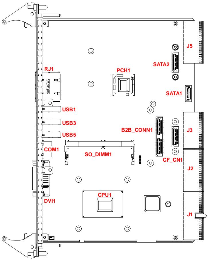
4.1 cPCI-6636(D) Component Side Layout
![RJ1\nUSB1\nUSB3\nUSB5\nCOM1\nSO_DIMM1\nDVI1\nPCH1\nB2B_CONN1\nCF_CN1\nCPU1\nSATA2\nSATA1\nJ5\nJ3\nJ2\nJ1](.cpci-6636-50-15111-2000-01-preliminary/fd47f6cdcf1d07ae9f6e1504b0f3c4728e1decd945af73bce7a29cda5ea24bba.jpg)

<table><tr><td>CPU1</td><td>Intel® processor</td><td>PCH1</td><td>Intel® PCH</td></tr><tr><td>SO_DIMM1</td><td>Memory socket</td><td>J1/J2/J3/5</td><td>CompactPCI connectors</td></tr><tr><td>CF_CN1 (CPCI-6636)</td><td>CFast board-to-board connector</td><td>B2B_CONN1 (cPCI-6636D/DZ)</td><td>XMC board-to-board connector</td></tr><tr><td>SATA1</td><td>7-pin SATA connector</td><td>SATA2</td><td>SATA board-to-board connector</td></tr></table>

Figure 4-1: cPCI-6636(D) Component Side Layout

# 4.2 cPCI-6636D/DZ Assembly Layoutt

![SATA Drive\nAssembly\nDB-6636XMC\nXMC Adapter\nCPU Heatsink](.cpci-6636-50-15111-2000-01-preliminary/eabc9be00ea7c22c0fa098b52885ad8abed13b9695fd3d54db416d9db5450931.jpg)

Figure 4-2: cPCI-6636D/DZ Assembly Layout

# 4.3 cPCI-6636(D/DZ) Faceplate I/O

cPCI-6636
![GbE x2\nUSB 3.0 x3\nSerial Port\nDVI-I\nReset\nButton\nPower LED\nHDD LED\nWDT LED](.cpci-6636-50-15111-2000-01-preliminary/6a54c3784edeb17d47357903cd71ec4b446942d1f062f2e9f8993258a2268698.jpg)

cPCI-6636D
![GbE x2\nUSB 3.0 x3\nSerial Port\nXMC\nDVI-I\nReset Button\nPower LED\nHDD LED\nWDT LED](.cpci-6636-50-15111-2000-01-preliminary/ae404c2c92605837e303668a13aeecbc959547ea66130685d2ca79602ffa02b7.jpg)

cPCI-6636DZ

![USB 3.0 x8\nGbE x2\nXMC\nVGA\nReset Button\nPower LED\nSerial Port x3\nHDD LED\nWDT LED\nVGA](.cpci-6636-50-15111-2000-01-preliminary/a1ab56073530e134f757f297efce9c5f2a5150f192c65781de8686ba54aa46b4.jpg)

Figure 4-3: cPCI-6636(D/DZ) Faceplate I/O

System LEDs

<table><tr><td>LED</td><td>Color</td><td>Condition</td><td>Indication</td></tr><tr><td rowspan="3">Power&lt;img src="images/f9f39d2111cc7bbcffe788fa853a19dbbd122f5261198e066b51a2f8917e1f51.jpg"/&gt;</td><td rowspan="3">Green/Red</td><td>Off</td><td>System is off</td></tr><tr><td>Red</td><td>System Power ready (PWGD)</td></tr><tr><td>Green</td><td>Post OK</td></tr><tr><td rowspan="2">WDT&lt;img src="images/7b8de3d13ee961055d9dac5f17fc026811e2262c041393a5e6a35b30bea269b6.jpg"/&gt;</td><td rowspan="2">Orange</td><td>Off</td><td>No Watchdog event</td></tr><tr><td>Blinking</td><td>Watchdog event alert</td></tr><tr><td rowspan="2">HDD[S W6S]</td><td rowspan="2">Yellow</td><td>Off</td><td>No CF/CFast/SATA HDD activity</td></tr><tr><td>Blinking</td><td>Data read/write in process for CFast/SATA drive</td></tr></table>

Table 4-1: cPCI-6636(D) Front Panel System LED Descriptions

# 4.4 Connector Pin Assignments

LAN1/2 RJ-45 GbE Connectors

<table><tr><td>Pin #</td><td>10BASE-T/100BASE-TX</td><td>1000BASE-T</td></tr><tr><td>1</td><td>TX+</td><td>LAN_TX0+</td></tr><tr><td>2</td><td>TX-</td><td>LAN_TX0-</td></tr><tr><td>3</td><td>RX+</td><td>LAN_TX1+</td></tr><tr><td>4</td><td>—</td><td>LAN_TX2+</td></tr><tr><td>5</td><td>—</td><td>LAN_TX2-</td></tr><tr><td>6</td><td>RX-</td><td>LAN_TX1-</td></tr><tr><td>7</td><td>—</td><td>LAN_TX3+</td></tr><tr><td>8</td><td>—</td><td>LAN_TX3-</td></tr></table>

Table 4-2: LAN1/2 RJ-45 GbE Pin Definitions

![Speed\nActivity\n8\n1](.cpci-6636-50-15111-2000-01-preliminary/8dc786fb21771807cf2cceb225176d8cf2f25b6be42b20923fc38814691fee32.jpg)

<table><tr><td colspan="2">Status</td><td>Speed LED (Green/Amber)</td><td>Activity LED (Yellow)</td></tr><tr><td colspan="2">Network link is not established or system powered off</td><td>OFF</td><td>OFF</td></tr><tr><td rowspan="2">10 Mbps</td><td>Link</td><td>OFF</td><td>ON</td></tr><tr><td>Active</td><td>OFF</td><td>Blinking</td></tr><tr><td rowspan="2">100 Mbps</td><td>Link</td><td>Green</td><td>ON</td></tr><tr><td>Active</td><td>Green</td><td>Blinking</td></tr><tr><td rowspan="2">1000 Mbps</td><td>Link</td><td>Amber</td><td>ON</td></tr><tr><td>Active</td><td>Amber</td><td>Blinking</td></tr></table>

Table 4-3: LAN LED Status Definitions

# USB 3.0 Connectors

<table><tr><td>Pin #</td><td>Signal Name</td></tr><tr><td>1</td><td>VCC</td></tr><tr><td>2</td><td>Data-</td></tr><tr><td>3</td><td>Data+</td></tr><tr><td>4</td><td>GND</td></tr><tr><td>5</td><td>RX_N</td></tr><tr><td>6</td><td>RX_P</td></tr><tr><td>7</td><td>GND</td></tr><tr><td>8</td><td>TX_N</td></tr><tr><td>9</td><td>TX_P</td></tr></table>

![9\n8\n7\n6\n5\n1\n2\n3\n4](.cpci-6636-50-15111-2000-01-preliminary/6d4998e8740022c54a49d50f12e127e34127615b7a5722b95c900ba820dbfb75.jpg)

Table 4-4: USB 3.0 Pin Definitions

# cPCI-6636(D) COM1 (RJ-45)

<table><tr><td>Pin #</td><td>RS-232</td><td>RS-422</td><td>RS-485</td></tr><tr><td>1</td><td>DCD#</td><td>TX-</td><td>Data-</td></tr><tr><td>2</td><td>RTS#</td><td>—</td><td>—</td></tr><tr><td>3</td><td>DSR#</td><td>—</td><td>—</td></tr><tr><td>4</td><td>TXD</td><td>RX+</td><td>—</td></tr><tr><td>5</td><td>RXD</td><td>TX+</td><td>Data+</td></tr><tr><td>6</td><td>GND</td><td>—</td><td>—</td></tr><tr><td>7</td><td>CTS#</td><td>—</td><td>—</td></tr><tr><td>8</td><td>DTR#L</td><td>RX-</td><td>—</td></tr></table>

![The image displays a technical diagram featuring a grey, bellows-like shape centered within a rectangular outline. Below the shape, the number '8' is on the left and the number '1' is on the right. Thin black lines connect the number '8' to the bottom left side of the inner shape and the number '1' to the bottom right side.](.cpci-6636-50-15111-2000-01-preliminary/e575c0a95267b458fe8fcc4cbc72a41fa33768cdcc91b46e123b5b8e946899c9.jpg)
Table 4-5: cPCI-6636(D) COM Pin Definitions

# cPCI-6636(D) COM RJ-45 to DB-9 Cable

(PN: 30-01020-0200)

<table><tr><td>Pin #</td><td>RS-232</td><td>RS-422</td><td>RS-485</td></tr><tr><td>1</td><td>DCD#</td><td>TX-</td><td>Data-</td></tr><tr><td>2</td><td>RXD</td><td>TX+</td><td>Data+</td></tr><tr><td>3</td><td>TXD</td><td>RX+</td><td>—</td></tr><tr><td>4</td><td>DTR#L</td><td>RX-</td><td>—</td></tr><tr><td>5</td><td>GND</td><td>—</td><td>—</td></tr><tr><td>6</td><td>DSR#</td><td>—</td><td>—</td></tr><tr><td>7</td><td>RTS#</td><td>—</td><td>—</td></tr><tr><td>8</td><td>CTS#</td><td>—</td><td>—</td></tr><tr><td>9</td><td>—</td><td>—</td><td>—</td></tr></table>

![6\n1\n5](.cpci-6636-50-15111-2000-01-preliminary/6d22c3acdfd242addff39a20eef8e13f9482f38f7a622d5d4145fea2f0c831e1.jpg)

Table 4-6: cPCI-6636(D) COM RJ-45 to DB-9 Cable Pin Definitions

# cPCI-6636DZ COM1-6 (RJ-45)

The three RJ-45 ports on the cPCI-6636DZ carry two sets of RX/TX signals each. From right to left: COM1/2, COM3/4 and COM5/6.

# COM1/2

<table><tr><td>Pin #</td><td>RS-232</td></tr><tr><td>1</td><td>P5V</td></tr><tr><td>2</td><td>COM1_RX</td></tr><tr><td>3</td><td>COM1_TX</td></tr><tr><td>4</td><td>GND</td></tr><tr><td>5</td><td>P5V</td></tr><tr><td>6</td><td>COM2_RX</td></tr><tr><td>7</td><td>COM2_TX</td></tr><tr><td>8</td><td>GND</td></tr></table>

![The image is a diagram featuring a square border around a central grey object that resembles an electrical plug. Two leader lines extend from the bottom corners of the object. The left line points to the number '8' and the right line points to the number '1'.](.cpci-6636-50-15111-2000-01-preliminary/b04dfd68d7d98f5b895245877d189321016c9079b7111bf84074f2c0e2b04809.jpg)
Table 4-7: cPCI-6636DZ COM1/2 Pin Definitions

# COM3/4

<table><tr><td>Pin #</td><td>RS-232</td></tr><tr><td>1</td><td>P5V</td></tr><tr><td>2</td><td>COM3_RX</td></tr><tr><td>3</td><td>COM3_TX</td></tr><tr><td>4</td><td>GND</td></tr><tr><td>5</td><td>P5V</td></tr><tr><td>6</td><td>COM4_RX</td></tr><tr><td>7</td><td>COM4_TX</td></tr><tr><td>8</td><td>GND</td></tr></table>

![This is a black and white line drawing of a connector, likely an RJ45 jack. It features a rectangular outline containing a central, darker, plug-like shape. Two lines extend from the bottom corners of this inner shape downwards. The left line points to the number **8**, and the right line points to the number **1**.](.cpci-6636-50-15111-2000-01-preliminary/0a6631f2812ad528dced6fd820c0dac51f85b0efdd1f7bf4ea041d177af1f7df.jpg)
Table 4-8: cPCI-6636DZ COM3/4 Pin Definitions

# COM5/6

<table><tr><td>Pin #</td><td>RS-232</td></tr><tr><td>1</td><td>P5V</td></tr><tr><td>2</td><td>COM3_RX</td></tr><tr><td>3</td><td>COM3_TX</td></tr><tr><td>4</td><td>GND</td></tr><tr><td>5</td><td>P5V</td></tr><tr><td>6</td><td>COM4_RX</td></tr><tr><td>7</td><td>COM4_TX</td></tr><tr><td>8</td><td>GND</td></tr></table>

![The image displays a schematic diagram of an RJ45 connector. At the bottom left, the number '8' is visible, and at the bottom right, the number '1' is visible. Thin black lines extend from each number upwards to touch the bottom corners of the central, grey-shaded connector plug illustration.](.cpci-6636-50-15111-2000-01-preliminary/735b7707da27c13b2cc0be442e6e7869cdd9cdcb29bda1c75b38e03a94ede6de.jpg)
Table 4-9: cPCI-6636DZ COM5/6 Pin Definitions

# cPCI-6636DZ COM RJ-45 to 2x DB-9 Cable

(PN: 30-25044-1020)

![Diagram of a USB connector showing two connected modules (no text or symbols)](.cpci-6636-50-15111-2000-01-preliminary/2829758c4fde0f9f219fa9603282a79dbfbfc147732dbc1afd166278fca3c39f.jpg)

The DB-9 connectors are labeled “01” and “02”. Connector “01” corresponds to the odd numbered COM signal on the RJ-45 connector, and connector “02” corresponds to the even numbered COM signal (i.e. “a” = “odd”, “b” = “even”).

<table><tr><td>Pin #</td><td>DB-9 “01”</td><td>DB-9 “02”</td></tr><tr><td>1</td><td>-</td><td>-</td></tr><tr><td>2</td><td>COMa_RX</td><td>COMb_RX</td></tr><tr><td>3</td><td>COMa_TX</td><td>COMb_TX</td></tr><tr><td>4</td><td>-</td><td>-</td></tr><tr><td>5</td><td>GNDa</td><td>GNDb</td></tr><tr><td>6</td><td>-</td><td>-</td></tr><tr><td>7</td><td>-</td><td>-</td></tr><tr><td>8</td><td>-</td><td>-</td></tr><tr><td>9</td><td>-</td><td>-</td></tr></table>

![6\n1\n5](.cpci-6636-50-15111-2000-01-preliminary/c9fa22be10b58e14bbfd8849d76163b7df4318bf81088862d4c977dafc5e504d.jpg)

Table 4-10: cPCI-6636DZ COM RJ-45 to 2x DB-9 Cable Pin Definitions

# DVI-I Connector

![Front view of a 24-pin D-sub connector (no text or symbols visible)](.cpci-6636-50-15111-2000-01-preliminary/1f53cc24e714afa357c2ed7f74cdb49d33024945814247aae49c0baf91135247.jpg)

<table><tr><td>Pin #</td><td>Signal</td><td>Pin #</td><td>Signal</td></tr><tr><td>1</td><td>TMDS Data2-</td><td>16</td><td>Hot Plug Detect</td></tr><tr><td>2</td><td>TMDS Data2+</td><td>17</td><td>TMDS Data0-</td></tr><tr><td>3</td><td>GND</td><td>18</td><td>TMDSData0+</td></tr><tr><td>4</td><td>NC</td><td>19</td><td>GND</td></tr><tr><td>5</td><td>NC</td><td>20</td><td>NC</td></tr><tr><td>6</td><td>DDC Clock [SCL]</td><td>21</td><td>NC</td></tr><tr><td>7</td><td>DDC Data [SDA]</td><td>22</td><td>GND</td></tr><tr><td>8</td><td>Analog vertical sync</td><td>23</td><td>TMDS Clock +</td></tr><tr><td>9</td><td>TMDS Data1-</td><td>24</td><td>TMDS Clock -</td></tr><tr><td>10</td><td>TMDS Data1+</td><td>C1</td><td>Analog Red</td></tr><tr><td>11</td><td>GND</td><td>C2</td><td>Analog Green</td></tr><tr><td>12</td><td>NC</td><td>C3</td><td>Analog Blue</td></tr><tr><td>13</td><td>NC</td><td>C4</td><td>Analog Horizontal Sync</td></tr><tr><td>14</td><td>+5 V Power</td><td>C5</td><td>Analog GND Return</td></tr><tr><td>15</td><td>GND</td><td></td><td></td></tr></table>

Table 4-11: DVI-I Connector Pin Definition

Serial ATA 7-pin Connector (SATA1)

<table><tr><td>Pin #</td><td>Signal</td></tr><tr><td>1</td><td>GND</td></tr><tr><td>2</td><td>TX+</td></tr><tr><td>3</td><td>TX-</td></tr><tr><td>4</td><td>GND</td></tr><tr><td>5</td><td>RX-</td></tr><tr><td>6</td><td>RX+</td></tr><tr><td>7</td><td>GND</td></tr></table>

![1\n7](.cpci-6636-50-15111-2000-01-preliminary/9d19a5ace790d0f5705dc469558849d5ac8e76776d24aa865e55a380553cf646.jpg)

Table 4-12: Serial ATA 7-pin Connector Pin Definition

# Serial ATA Connector with Power

2.5" SATA adapter board (PN: 59-37571-0000)

<table><tr><td>Pin #</td><td>Signal</td></tr><tr><td>S1</td><td>GND</td></tr><tr><td>S2</td><td>TX+</td></tr><tr><td>S3</td><td>TX-</td></tr><tr><td>S4</td><td>GND</td></tr><tr><td>S5</td><td>RX-</td></tr><tr><td>S6</td><td>RX+</td></tr><tr><td>S7</td><td>GND</td></tr><tr><td>P1</td><td>NC</td></tr><tr><td>P2</td><td>NC</td></tr><tr><td>P3</td><td>NC</td></tr><tr><td>P4</td><td>GND</td></tr><tr><td>P5</td><td>GND</td></tr><tr><td>P6</td><td>GND</td></tr><tr><td>P7</td><td>5V</td></tr><tr><td>P8</td><td>5V</td></tr><tr><td>P9</td><td>5V</td></tr><tr><td>P10</td><td>GND</td></tr><tr><td>P11</td><td>NC</td></tr><tr><td>P12</td><td>GND</td></tr><tr><td>P13~P15</td><td>NC</td></tr></table>

![S1\nSignal\nS7\nP1\nPower\nP15](.cpci-6636-50-15111-2000-01-preliminary/f2cec3fb3e325f80102c8ac6a0e28c4c9cb0f2165c8eb7a5af73ef37b46440c0.jpg)

Table 4-13: Serial ATA Connector with power Pin Definition

# CFast Socket

DB-CFAST adapter board (PN: 59-37572-0000)

<table><tr><td>Pin #</td><td>Signal Name</td></tr><tr><td>Ground</td><td>S1</td></tr><tr><td>SATA_TX-P</td><td>S2</td></tr><tr><td>SATA_TX-N</td><td>S3</td></tr><tr><td>Ground</td><td>S4</td></tr><tr><td>SATA_RX-N</td><td>S5</td></tr><tr><td>SATA_RX-P</td><td>S6</td></tr><tr><td>Ground</td><td>S7</td></tr><tr><td>CFast_CDI</td><td>P1</td></tr><tr><td>Ground</td><td>P2</td></tr><tr><td>NC</td><td>P3</td></tr><tr><td>NC</td><td>P4</td></tr><tr><td>NC</td><td>P5</td></tr><tr><td>NC</td><td>P6</td></tr><tr><td>Ground</td><td>P7</td></tr><tr><td>CFast_LED1</td><td>P8</td></tr><tr><td>CFast_LED2</td><td>P9</td></tr><tr><td>NC</td><td>P10</td></tr><tr><td>NC</td><td>P11</td></tr><tr><td>NC</td><td>P12</td></tr><tr><td>+3.3V</td><td>P13</td></tr><tr><td>+3.3V</td><td>P14</td></tr><tr><td>Ground</td><td>P15</td></tr><tr><td>Ground</td><td>P16</td></tr><tr><td>CFast_CDO</td><td>P17</td></tr></table>

![Pure electrical connector diagram without any text, numbers, or symbols](.cpci-6636-50-15111-2000-01-preliminary/c4666caa8755dde604b64b08faa930786c0048d9241624ddfef27923e84283b3.jpg)

![24\nP1\nS1](.cpci-6636-50-15111-2000-01-preliminary/a1d074f6e6b18ef887fadd4e66bdf41a9a373d78ae8834c5f8c4c685e4faa07b.jpg)

Table 4-14: CFast Socket Pin Definition

CompactPCI J1 Connector

<table><tr><td>Pin</td><td>Z</td><td>A</td><td>B</td><td>C</td><td>D</td><td>E</td><td>F</td></tr><tr><td>25</td><td>GND</td><td>P5V</td><td>CPCI_REQ64-L</td><td>CPCI_ENUM-L</td><td>P3V3</td><td>P5V</td><td>GND</td></tr><tr><td>24</td><td>GND</td><td>CPCI_AD1</td><td>P5V</td><td>CPCI_VIO_STB</td><td>AD0</td><td>CPCI_ACK64-L</td><td>GND</td></tr><tr><td>23</td><td>GND</td><td>P3V3</td><td>CPCI_AD4</td><td>CPCI_AD3</td><td>P5V</td><td>CPCI_AD2</td><td>GND</td></tr><tr><td>22</td><td>GND</td><td>CPCI_AD7</td><td>GND</td><td>P3V3</td><td>CPCI_AD6</td><td>CPCI_AD5</td><td>GND</td></tr><tr><td>21</td><td>GND</td><td>P3V3</td><td>CPCI_AD9</td><td>CPCI_AD8</td><td>CPCI_M66EN</td><td>CPCI_CBE-L0</td><td>GND</td></tr><tr><td>20</td><td>GND</td><td>CPCI_AD12</td><td>GND</td><td>CPCI_VIO_STB</td><td>CPCI_AD11</td><td>CPCI_AD10</td><td>GND</td></tr><tr><td>19</td><td>GND</td><td>P3V3</td><td>CPCI_AD15</td><td>CPCI_AD14</td><td>GND</td><td>CPCI_AD13</td><td>GND</td></tr><tr><td>18</td><td>GND</td><td>CPCI_SERR-L</td><td>GND</td><td>P3V3</td><td>CPCI_PAR</td><td>CPCI_CBE-L1</td><td>GND</td></tr><tr><td>17</td><td>GND</td><td>P3V3</td><td>IPMB_CLK</td><td>IPMB_DAT</td><td>GND</td><td>CPCI_PERR-L</td><td>GND</td></tr><tr><td>16</td><td>GND</td><td>CPCI_DEVSEL-L</td><td>GND</td><td>CPCI_VIO_STB</td><td>CPCI_STOP-L</td><td>CPCI_LOCK-L</td><td>GND</td></tr><tr><td>15</td><td>GND</td><td>P3V3</td><td>CPCI_FRAME-L</td><td>CPCI_IRDY-L</td><td>CPCI_BDSEL-L</td><td>CPCI_TRDY-L</td><td>GND</td></tr><tr><td>12-14</td><td colspan="7">Key Area</td></tr><tr><td>11</td><td>GND</td><td>CPCI_AD18</td><td>CPCI_AD17</td><td>CPCI_AD16</td><td>GND</td><td>CPCI_CBE-L2</td><td>GND</td></tr><tr><td>10</td><td>GND</td><td>CPCI_AD21</td><td>GND</td><td>P3V3</td><td>CPCI_AD20</td><td>CPCI_AD19</td><td>GND</td></tr><tr><td>9</td><td>GND</td><td>CPCI_CBE-L3</td><td>CPCI_IDSEL</td><td>CPCI_AD23</td><td>GND</td><td>CPCI_AD22</td><td>GND</td></tr><tr><td>8</td><td>GND</td><td>CPCI_AD26</td><td>GND</td><td>CPCI_VIO_STB</td><td>CPCI_AD25</td><td>CPCI_AD24</td><td>GND</td></tr><tr><td>7</td><td>GND</td><td>CPCI_AD30</td><td>CPCI_AD29</td><td>CPCI_AD28</td><td>GND</td><td>CPCI_AD27</td><td>GND</td></tr><tr><td>6</td><td>GND</td><td>CPCI_REQ-L0</td><td>CPCI_PRESENT-L</td><td>P3V3</td><td>CPCI_CLK0</td><td>CPCI_AD31</td><td>GND</td></tr><tr><td>5</td><td>GND</td><td>NC</td><td>NC</td><td>CPCI_RET-L</td><td>GND</td><td>CPCI_GNT-L0</td><td>GND</td></tr><tr><td>4</td><td>GND</td><td>P5V_IPMB</td><td>CPCI_HEALTHY-L</td><td>CPCI_VIO_STB</td><td>CPCI_INTP</td><td>CPCI_INTS</td><td>GND</td></tr><tr><td>3</td><td>GND</td><td>CPCI_INTA-L</td><td>CPCI_INTB-L</td><td>CPCI_INTC-L</td><td>P5V</td><td>CPCI_INTD-L</td><td>GND</td></tr><tr><td>2</td><td>GND</td><td>GND</td><td>P5V</td><td>NC</td><td>NC</td><td>NC</td><td>GND</td></tr><tr><td>1</td><td>GND</td><td>P5V</td><td>N12V</td><td>NC</td><td>P12V</td><td>P5V</td><td>GND</td></tr></table>

Table 4-15: CompactPCI J1 Connector Pin Definition

CompactPCI J2 Connector

<table><tr><td>Pin</td><td>Z</td><td>A</td><td>B</td><td>C</td><td>D</td><td>E</td><td>F</td></tr><tr><td>22</td><td>GND</td><td>GA4</td><td>GA3</td><td>GA2</td><td>GA1</td><td>GA0</td><td>GND</td></tr><tr><td>21</td><td>GND</td><td>CPCI_CLK6</td><td>GND</td><td>NC</td><td>NC</td><td>NC</td><td>GND</td></tr><tr><td>20</td><td>GND</td><td>CPCI_CLK5</td><td>GND</td><td>NC</td><td>GND</td><td>NC</td><td>GND</td></tr><tr><td>19</td><td>GND</td><td>GND</td><td>GND</td><td>IPMB_DAT</td><td>IPMB_CLK</td><td>IPMB_PWR</td><td>GND</td></tr><tr><td>18</td><td>GND</td><td>NC</td><td>NC</td><td>NC</td><td>GND</td><td>NC</td><td>GND</td></tr><tr><td>17</td><td>GND</td><td>NC</td><td>GND</td><td>J2_RST-L</td><td>CPCI_REQ-L6</td><td>CPCI_GNT-L6</td><td>GND</td></tr><tr><td>16</td><td>GND</td><td>NC</td><td>NC</td><td>CPCI_DEG-L</td><td>GND</td><td>NC</td><td>GND</td></tr><tr><td>15</td><td>GND</td><td>NC</td><td>GND</td><td>CPCI_FAL-L</td><td>CPCI_REQ-L5</td><td>CPCI_GNT-L5</td><td>GND</td></tr><tr><td>14</td><td>GND</td><td>CPCI_AD35</td><td>CPCI_AD34</td><td>CPCI_AD33</td><td>GND</td><td>CPCI_AD32</td><td>GND</td></tr><tr><td>13</td><td>GND</td><td>CPCI_AD38</td><td>GND</td><td>CPCI_VIO</td><td>CPCI_AD37</td><td>CPCI_AD36</td><td>GND</td></tr><tr><td>12</td><td>GND</td><td>CPCI_AD42</td><td>CPCI_AD41</td><td>CPCI_AD40</td><td>GND</td><td>CPCI_AD39</td><td>GND</td></tr><tr><td>11</td><td>GND</td><td>CPCI_AD45</td><td>GND</td><td>CPCI_VIO</td><td>CPCI_AD44</td><td>CPCI_AD43</td><td>GND</td></tr><tr><td>10</td><td>GND</td><td>CPCI_AD49</td><td>CPCI_AD48</td><td>CPCI_AD47</td><td>GND</td><td>CPCI_AD46</td><td>GND</td></tr><tr><td>9</td><td>GND</td><td>CPCI_AD52</td><td>GND</td><td>CPCI_VIO</td><td>CPCI_AD51</td><td>CPCI_AD50</td><td>GND</td></tr><tr><td>8</td><td>GND</td><td>CPCI_AD56</td><td>CPCI_AD55</td><td>CPCI_AD54</td><td>GND</td><td>CPCI_AD53</td><td>GND</td></tr><tr><td>7</td><td>GND</td><td>CPCI_AD59</td><td>GND</td><td>CPCI_VIO</td><td>CPCI_AD58</td><td>CPCI_AD57</td><td>GND</td></tr><tr><td>6</td><td>GND</td><td>CPCI_AD63</td><td>CPCI_AD62</td><td>CPCI_AD61</td><td>GND</td><td>CPCI_AD60</td><td>GND</td></tr><tr><td>5</td><td>GND</td><td>CPCI_CBE-L5</td><td>CPCI_DEV64-L</td><td>CPCI_VIO</td><td>CPCI_CBE-L4</td><td>CPCI_PAR64</td><td>GND</td></tr><tr><td>4</td><td>GND</td><td>CPCI_VIO</td><td>NC</td><td>CPCI_CBE-L7</td><td>GND</td><td>CPCI_CBE-L6</td><td>GND</td></tr><tr><td>3</td><td>GND</td><td>CPCI_CLK4</td><td>GND</td><td>CPCI_GNT-L3</td><td>CPCI_REQ-L4</td><td>CPCI_GNT-L4</td><td>GND</td></tr><tr><td>2</td><td>GND</td><td>CPCI_CLK2</td><td>CPCI_CLK3</td><td>SYSEN-L</td><td>CPCI_GNT-L2</td><td>CPCI_REQ-L3</td><td>GND</td></tr><tr><td>1</td><td>GND</td><td>CPCI_CLK1</td><td>GND</td><td>CPCI_REQ-L1</td><td>CPCI_GNT-L1</td><td>CPCI_REQ-L2</td><td>GND</td></tr></table>

Table 4-16: CompactPCI J2 Connector Pin Definition

CompactPCI J3 Connector

<table><tr><td>Pin</td><td>Z</td><td>A</td><td>B</td><td>C</td><td>D</td><td>E</td><td>F</td></tr><tr><td>19</td><td>GND</td><td>P5V</td><td>P5V</td><td>P12V</td><td>P5V</td><td>P5V</td><td>GND</td></tr><tr><td>18</td><td>GND</td><td>LAN4_MDI0_P</td><td>LAN4_MDI0_N</td><td>GND</td><td>LAN4_MDI2_P</td><td>LAN4_MDI2_N</td><td>GND</td></tr><tr><td>17</td><td>GND</td><td>LAN4_MDI1_P</td><td>LAN4_MDI1_N</td><td>GND</td><td>LAN4_MDI3_P</td><td>LAN4_MDI3_N</td><td>GND</td></tr><tr><td>16</td><td>GND</td><td>LAN3_MDI0_P</td><td>LAN3_MDI0_N</td><td>GND</td><td>LAN3_MDI2_P</td><td>LAN3_MDI2_N</td><td>GND</td></tr><tr><td>15</td><td>GND</td><td>LAN3_MDI1_P</td><td>LAN3_MDI1_N</td><td>GND</td><td>LAN3_MDI3_P</td><td>LAN3_MDI3_N</td><td>GND</td></tr><tr><td>14</td><td>GND</td><td>USB_OC5-L</td><td>USB_OC6-L</td><td>USB_OC7-L</td><td>USB_OC8-L</td><td>USB_OC9-L</td><td>GND</td></tr><tr><td>13</td><td>GND</td><td>USB8-P</td><td>USB8-N</td><td>GND</td><td>USB9-P</td><td>USB9-N</td><td>GND</td></tr><tr><td>12</td><td>GND</td><td>USB6-P</td><td>USB6-N</td><td>GND</td><td>USB7-P</td><td>USB7-N</td><td>GND</td></tr><tr><td>11</td><td>GND</td><td>USB4-P</td><td>USB4-N</td><td>GND</td><td>USB5-P</td><td>USB5-N</td><td>GND</td></tr><tr><td>10</td><td>GND</td><td>USB_OC4-L</td><td>CRT_CLK</td><td>CRT_DAT</td><td>CRT_HSYNC</td><td>CRT_VSYNC</td><td>GND</td></tr><tr><td>9</td><td>GND</td><td>COM3_CTS-L</td><td>COM3_RI-L</td><td>CRT_BLUE</td><td>CRT_RED</td><td>CRT_GREEN</td><td>GND</td></tr><tr><td>8</td><td>GND</td><td>COM3_RXD</td><td>COM3_TXD</td><td>COM3_DTR-L</td><td>COM3_DSR-L</td><td>COM3_RTS-L</td><td>GND</td></tr><tr><td>7</td><td>GND</td><td>COM4_TX</td><td>COM4_RX</td><td>COM3_DCD-L</td><td>GPIO</td><td>GPIO</td><td>GND</td></tr><tr><td>6</td><td>GND</td><td>SATA1_RXPC</td><td>SATA1_RXNC</td><td>GND</td><td>SATA0_RXPC</td><td>SATA0_RXNC</td><td>GND</td></tr><tr><td>5</td><td>GND</td><td>GND</td><td>GND</td><td>NC</td><td>GND</td><td>GND</td><td>GND</td></tr><tr><td>4</td><td>GND</td><td>SATA1_TXPC</td><td>SATA1_TXNC</td><td>GND</td><td>SATA0_TXPC</td><td>SATA0_TXNC</td><td>GND</td></tr><tr><td>3</td><td>GND</td><td>KBDATA</td><td>KBCLK</td><td>GPIO2</td><td>MSDATA</td><td>MSCLK</td><td>GND</td></tr><tr><td>2</td><td>GND</td><td>A_HDA_SDIN1</td><td>AUD_SDIN2</td><td>NC</td><td>AUD_DOCK_EN-L</td><td>AUD_DOCK_RST-L</td><td>GND</td></tr><tr><td>1</td><td>GND</td><td>A_HDA_RST-L</td><td>A_HDA_SYNC</td><td>A_HDA_BIT_CLK</td><td>A_HDA_SDOUT</td><td>A_HDA_SDIN0</td><td>GND</td></tr><tr><td></td><td>Z</td><td>A</td><td>B</td><td>C</td><td>D</td><td>E</td><td>F</td></tr></table>

Table 4-17: CompactPCI J3 Connector Pin Definition

CompactPCI J5 Connector

<table><tr><td>Pin</td><td>Z</td><td>A</td><td>B</td><td>C</td><td>D</td><td>E</td><td>F</td></tr><tr><td>22</td><td>GND</td><td>LAN2_MDI_P0</td><td>LAN2_MDI_N0</td><td>GND</td><td>LAN2_MDI_P2</td><td>LAN2_MDI_N2</td><td>GND</td></tr><tr><td>21</td><td>GND</td><td>LAN2_MDI_P1</td><td>LAN2_MDI_N1</td><td>GND</td><td>LAN2_MDI_P3</td><td>LAN2_MDI_N3</td><td>GND</td></tr><tr><td>20</td><td>GND</td><td>LAN1_MDI_P0</td><td>LAN1_MDI_N0</td><td>GND</td><td>LAN1_MDI_P2</td><td>LAN1_MDI_N2</td><td>GND</td></tr><tr><td>19</td><td>GND</td><td>LAN1_MDI_P1</td><td>LAN1_MDI_N1</td><td>GND</td><td>LAN1_MDI_P3</td><td>LAN1_MDI_N3</td><td>GND</td></tr><tr><td>18</td><td>GND</td><td>DVID_CLKP</td><td>DVID_CLKN</td><td>GND</td><td>GND</td><td>GND</td><td>GND</td></tr><tr><td>17</td><td>GND</td><td>DVID_TXP1</td><td>DVID_TXN1</td><td>GND</td><td>COM2_TX</td><td>COM2_RX</td><td>GND</td></tr><tr><td>16</td><td>GND</td><td>DVID_SDA</td><td>DVID_SCL</td><td>DVID_HPD</td><td>GND</td><td>GND</td><td>GND</td></tr><tr><td>15</td><td>GND</td><td>DVID_TXP2</td><td>DVID_TXN2</td><td>GND</td><td>SATA_RX3_P_C</td><td>SATA_RX3_N_C</td><td>GND</td></tr><tr><td>14</td><td>GND</td><td>DVID_TXP0</td><td>DVID_TXN0</td><td>GND</td><td>SATA-TX3_P_C</td><td>SATA-TX3_N_C</td><td>GND</td></tr><tr><td>13</td><td>GND</td><td>LAN3_LED_100-L</td><td>LAN4_LED_100-L</td><td>REAR_GPIO6</td><td>LAN4_LED_1000-L</td><td>LAN3_LED_1000-L</td><td>GND</td></tr><tr><td>12</td><td>GND</td><td>DVI_SDA_RTM</td><td>DVI_SCL_RTM</td><td>DVI_HPD_RTM</td><td>RTM_HDD_LED</td><td>RTM_WDT_LED</td><td>GND</td></tr><tr><td>11</td><td>GND</td><td>DVIB_TX2_P_C</td><td>DVIB_TX2_N_C</td><td>GND</td><td>DVIB_CLK_P_C</td><td>DVIB_CLK_N_C</td><td>GND</td></tr><tr><td>10</td><td>GND</td><td>DVIB_TX0_P_C</td><td>DVIB_TX0_N_C</td><td>GND</td><td>DVIB_TX1_P_C</td><td>DVIB_TX1_N_C</td><td>GND</td></tr><tr><td>9</td><td>GND</td><td>REAR_GPIO1</td><td>REAR_GPIO2</td><td>REAR_GPIO3</td><td>REAR_GPIO4</td><td>REAR_GPIO5</td><td>GND</td></tr><tr><td>8</td><td>GND</td><td>LAN3_ACT-L</td><td>REAR_GPIO7</td><td>LAN4_ACT-L</td><td>REAR_GPIO8</td><td>REAR_GPIO9</td><td>GND</td></tr><tr><td>7</td><td>GND</td><td>GND</td><td>GND</td><td>BAT_RTM</td><td>GND</td><td>GND</td><td>GND</td></tr><tr><td>6</td><td>GND</td><td>CLK_REAR-P</td><td>CLK_REAR-N</td><td>GND</td><td>PLTRST_REAR-L</td><td>GPIO</td><td>GND</td></tr><tr><td>5</td><td>GND</td><td>GND</td><td>GND</td><td>GND</td><td>GND</td><td>GND</td><td>GND</td></tr><tr><td>4</td><td>GND</td><td>PCIE_TX8-P</td><td>PCIE_TX8-N</td><td>GND</td><td>PCIE_RX8-P</td><td>PCIE_RX8-N</td><td>GND</td></tr><tr><td>3</td><td>GND</td><td>PCIE_TX7-P</td><td>PCIE_TX7-N</td><td>GND</td><td>PCIE_RX7-P</td><td>PCIE_RX7-N</td><td>GND</td></tr><tr><td>2</td><td>GND</td><td>PCIE_TX6-P</td><td>PCIE_TX6-N</td><td>GND</td><td>PCIE_RX6-P</td><td>PCIE_RX6-N</td><td>GND</td></tr><tr><td>1</td><td>GND</td><td>PCIE_TX5-P</td><td>PCIE_TX5-N</td><td>GND</td><td>PCIE_RX5-P</td><td>PCIE_RX5-N</td><td>GND</td></tr><tr><td></td><td>Z</td><td>A</td><td>B</td><td>C</td><td>D</td><td>E</td><td>F</td></tr></table>

Table 4-18: CompactPCI J5 Connector Pin Definition

![The image displays a white sheet of paper icon with a folded top-right corner and faint horizontal lines running across it. A large, bold red checkmark is superimposed over the center of the paper.](.cpci-6636-50-15111-2000-01-preliminary/3367671e2e3df043c77a8b2029e3c6e8054d88d2842c3ecb4bb2bd15d5c33ecc.jpg)
NOTE:

GPIO signals to J5 are from the PCH. Contact ADLINK for information on how to control these GPIO.

# 4.5 Switches and Buttons

![SW3\nSW1\nSW2](.cpci-6636-50-15111-2000-01-preliminary/ced8a6a3c8a0592cca4ae9143a1ed3da21463f95569479d8c0ce2c301fd2eca2.jpg)

Figure 4-4: cPCI-6636 Series Switch Locations - Component Side

![SW5\nSW4\nSW6](.cpci-6636-50-15111-2000-01-preliminary/d553b8f09f25ef400133856234db46aff266671c50ad10a9a5f7e41de4a80678.jpg)

Figure 4-5: cPCI-6636 Series Switch Locations - Solder Side

# VGA Signal Front/Rear Switch (SW1 Pin 1, Reserved)

VGA functionality is controlled by BIOS.

# BIOS Protection Switch (SW1 Pin 2)

Enabling BIOS protection prevents changes to be made to the BIOS settings (enabled by default).

![ON\n1 2](.cpci-6636-50-15111-2000-01-preliminary/7bb394aed98ed9c898e8f814e6561336b763247b35bf98cf39903723d871fe9a.jpg)

<table><tr><td>SW1 Pin</td><td>ON</td><td>OFF</td></tr><tr><td>1</td><td>Reserved</td><td>Reserved (default)</td></tr><tr><td>2</td><td>BIOS Protection Enabled (default)</td><td>BIOS Protection Disabled</td></tr></table>

# Debug Switch (SW2, Reserved)

The default setting for SW2 is 1 OFF, 2 OFF. Do not change the settings unless instructed by ADLINK.

![ON\n1 2](.cpci-6636-50-15111-2000-01-preliminary/9baa29ec886d46e60f7a3da71361e62da5607d765535264a1932820930eb6120.jpg)

# LAN (RJ1) Front/Rear Switch (SW3, Reserved)

Default all OFF.

![ON\n1 2](.cpci-6636-50-15111-2000-01-preliminary/6f73efc980aa2909d7587beca46c3c82a6a01939b3154efe042a2f12d7eb71c4.jpg)

# COM1 Mode Switch (SW4)

cPCI-6636(D) only.

<table><tr><td>Pin</td><td>Function</td></tr><tr><td>1 OFF, 2 ON (default)</td><td>RS-232</td></tr><tr><td>1 ON, 2 OFF</td><td>RS-485</td></tr><tr><td>1 ON, 2 ON</td><td>RS-422</td></tr><tr><td>3</td><td>OFF (Reserved)</td></tr><tr><td>4</td><td>OFF (Reserved)</td></tr></table>

![ON\n1 2 3 4](.cpci-6636-50-15111-2000-01-preliminary/879e6b153b080c5c2dd49f5c0c72f162c47a9e582bb7c121d618371f00c704f7.jpg)

# System Reset Button (SW5)

Press switch SW5 to reset the system.

![Simple diagram showing a red arrow pointing to a black rectangle, no text or symbols present](.cpci-6636-50-15111-2000-01-preliminary/ce02c01d97502c97ba01f9f908bb8228f665d6bf18df071504537a2d724fd7b8.jpg)

# Force Ejector Handle Closed Switch (SW6)

Switch SW6 allows the ejector handle state to be forced "closed" so that blades without ejector handles (e.g. conduction cooled) will power on when inserted into the chassis.

<table><tr><td>Pin</td><td>ON</td><td>OFF</td></tr><tr><td>1</td><td>Force the ejector handle state to &quot;closed&quot; (default)</td><td>On/Off state is controlled by the ejector handle</td></tr><tr><td>2</td><td>NC</td><td>NC (default)</td></tr></table>

![ON\n1 2](.cpci-6636-50-15111-2000-01-preliminary/d6f8d487b6f28c0b436c6f3a092bb81b51a9b243a90c74f1e00cb5f9af9dcda3.jpg)

![The image displays a simple icon of a white document with a black border and faint horizontal lines, featuring a large red checkmark overlaid on the right side.](.cpci-6636-50-15111-2000-01-preliminary/fa0b6a710af89e8fb5bd18dde5541a7dd73aaf5af9af12e715d62037b79787e8.jpg)
NOTE:

When the On/Off state is controlled by the ejector handle (Pin 1 OFF), make sure to properly shut down the OS before opening the handle. If the ejector handle is opened while the OS is operating, power will be cut immediately, resulting in possible system corruption and data loss.

This page intentionally left blank.

# Important Safety Instructions

For user safety, please read and follow all instructions, WARNINGS, CAUTIONS, and NOTES marked in this manual and on the associated equipment before handling/operating the equipment.

▶ Read these safety instructions carefully.
- Keep this user’s manual for future reference.
▶ Read the specifications section of this manual for detailed information on the operating environment of this equipment.
▶ When installing/mounting or uninstalling/removing equipment:

▷ Turn off power and unplug any power cords/cables.

▶ To avoid electrical shock and/or damage to equipment:

▷ Keep equipment away from water or liquid sources;
▷ Keep equipment away from high heat or high humidity;
▷ Keep equipment properly ventilated (do not block or cover ventilation openings);

▶ Make sure to use recommended voltage and power source settings;

▶ Always install and operate equipment near an easily accessible electrical socket-outlet;

▷ Secure the power cord (do not place any object on/over the power cord);

▶ Only install/attach and operate equipment on stable surfaces and/or recommended mountings; and,

▷ If the equipment will not be used for long periods of time, turn off and unplug the equipment from its power source.

▶ Never attempt to fix the equipment. Equipment should only be serviced by qualified personnel.

A Lithium-type battery may be provided for uninterrupted, backup or emergency power.

![The image displays a standard warning symbol consisting of a dark red equilateral triangle pointing upward. Inside the triangle is a white exclamation point. Below the triangle, the word 'WARNING' is printed in black, uppercase letters.](.cpci-6636-50-15111-2000-01-preliminary/8b9ad9d19af97caf27666694017ac701b7078aef4e7a31d65e55e9496ab4be77.jpg)

Risk of explosion if battery is replaced with one of an incorrect type. Dispose of used batteries appropriately.

▶ Equipment must be serviced by authorized technicians when:

▷ The power cord or plug is damaged;
▷ Liquid has penetrated the equipment;
▷ It has been exposed to high humidity/moisture;
$\triangleright$ It is not functioning or does not function according to the user's manual;
▷ It has been dropped and/or damaged; and/or,
▷ It has an obvious sign of breakage.

# Getting Service

Ask an Expert: http://askanexpert.adlinktech.com

# ADLINK Technology, Inc.

9F, No.166 Jian Yi Road, Zhonghe District

New Taipei City 235, Taiwan

Tel: +886-2-8226-5877

Fax: +886-2-8226-5717

Email: service@adlinktech.com

# Ampro ADLINK Technology, Inc.

5215 Hellyer Avenue, #110

San Jose, CA 95138, USA

Tel: +1-408-360-0200

Toll Free: +1-800-966-5200 (USA only)

Fax: +1-408-360-0222

Email: info@adlinktech.com

# ADLINK Technology (China) Co., Ltd.

300 Fang Chun Rd., Zhangjiang Hi-Tech Park

Pudong New Area, Shanghai, 201203 China

Tel: +86-21-5132-8988

Fax: +86-21-5132-3588

Email: market@adlinktech.com

# ADLINK Technology GmbH

Hans-Thoma-Strasse 11

D-68163 Mannheim, Germany

Tel: +49-621-43214-0

Fax: +49-621 43214-30

Email: emea@adlinktech.com

Please visit the Contact page at www.adlinktech.com for information on how to contact the ADLINK regional office nearest you.
[🔗 Link to the original document](.cpci-6636-50-15111-2000-01-preliminary/cpci-6636-50-15111-2000-01-preliminary.pdf)
