# cPCI-6910 Series

6U CompactPCI $^{®}$ Single Board Computer with Dual-Core Intel $^{®}$ Xeon $^{®}$ Processor LV/ULV

User's Manual

Manual Revision: 2.05

Revision Date: June 6, 2008

Part No: 50-15056-1030

![Circular black-and-white recycling symbol with three white arrows forming a triangle (no text or symbols)](.cpci-6910-manual-13/59cbbc3adf362b5b148dc0f52656925119b0d8ec7ff670116f2e969c62164dca.jpg)

Recycled Paper

# Revision History

<table><tr><td>Version</td><td>Release Date</td><td>Revision(s)</td></tr><tr><td>2.00</td><td>2006/12/29</td><td>First release.</td></tr><tr><td rowspan="6">2.01</td><td rowspan="6">2007/04/04</td><td>Added power consumption data.</td></tr><tr><td>Updated J1 to J5 pin assignment.</td></tr><tr><td>Added RJ-45 COM pin-out.</td></tr><tr><td>Updated SW1 function description.</td></tr><tr><td>Modified various installations in Chapter 5: Getting Started.</td></tr><tr><td>Added CF adapter information (supports CF by adapter design on front board).</td></tr><tr><td rowspan="6">2.02</td><td rowspan="6">2007/07/19</td><td>Modified cPCI-6910 with cPCI-R6910 Block Diagram.</td></tr><tr><td>Updated SWZ2 function description.</td></tr><tr><td>Updated Onboard Devices descriptions.</td></tr><tr><td>Updated IPMI Sensor Lists.</td></tr><tr><td>Updated Firmware Revision History.</td></tr><tr><td>Added Switch information for RTM configuration.</td></tr><tr><td rowspan="6">2.03</td><td rowspan="6">2007/08/08</td><td>Added new cPCI-6910 Configuration options.</td></tr><tr><td>Added CPU specifications.</td></tr><tr><td>Added power consumption specifications under idle DOS, idle Linux®, full-load Windows® XP and idle Windows® XP environments.</td></tr><tr><td>Revised Firmware revision history information.</td></tr><tr><td>Added Voltage, Amperage and wattage units on power consumption tables.</td></tr><tr><td>Updated switch function information</td></tr><tr><td rowspan="9">2.04</td><td rowspan="9">2008/02/25</td><td>Revised CompactPCI® J3 Pin Assignments</td></tr><tr><td>Revised Oem Command Summary Table</td></tr><tr><td>Revised BMR-AVR-cPCI Supported Command List</td></tr><tr><td>Revised Onboard Device BIOS descriptions</td></tr><tr><td>Revised USB 2.0 Controller descriptions</td></tr><tr><td>Updated Block Diagram</td></tr><tr><td>Revised CompactPCI J2 Pin Assignments</td></tr><tr><td>Revised RJ-45 Connector Pin Assignments</td></tr><tr><td>Revised OemShowRevision Table</td></tr><tr><td rowspan="2">2.05</td><td rowspan="2">2008/06/06</td><td>Correct LAN status table</td></tr><tr><td>Correct address</td></tr></table>

This page intentionally left blank.

# Preface

# Copyright 2008 ADLINK TECHNOLOGY INC.

This document contains proprietary information protected by copyright. All rights are reserved. No part of this manual may be reproduced by any mechanical, electronic, or other means in any form without prior written permission of the manufacturer.

# Disclaimer

The information in this document is subject to change without prior notice in order to improve reliability, design, and function and does not represent a commitment on the part of the manufacturer.

In no event will the manufacturer be liable for direct, indirect, special, incidental, or consequential damages arising out of the use or inability to use the product or documentation, even if advised of the possibility of such damages.

# Trademarks

Microsoft $^{®}$ , MS-DOS $^{®}$ , Windows $^{®}$ 98, Windows $^{®}$ 98 SE, Windows $^{®}$ 2000, Windows $^{®}$ XP, Windows $^{®}$ XP Professional, and Windows $^{®}$ Server 2003 are registered trademarks of Microsoft $^{®}$ Corporation. Intel $^{®}$ Celeron $^{®}$ M, Xeon $^{®}$ , and SpeedStep $^{®}$ are registered trademarks of Intel $^{®}$ Corporation. CompactFlash $^{®}$ is a registered trademark of Sandisk $^{®}$ Corporation. Phoenix Award $^{™}$ BIOS is a trademark of Phoenix $^{®}$ Technologies Inc. CompactPCI $^{®}$ and PICMG $^{®}$ are registered trademarks of the PCI Industrial Computer Manufacturers Group. PCI Express $^{®}$ is a registered trademark of the Peripheral Component Interconnect Special Interest Group. LSI $^{®}$ Logic is a registered trademark of LSI Corporation. Linux $^{®}$ is a registered trademark of Linus Torvalds. PLX FastLane $^{™}$ is a trademark of PLX Technology, Inc. VxWorks $^{®}$ is a registered trademark of Wind River.

Product names mentioned herein are used for identification purposes only and may be trademarks and/or registered trademarks of their respective companies.

# Using this Manual

# Audience and Scope

The cPCI-6910 Series User's Manual is intended for hardware technicians and systems operators with knowledge of installing, configuring and operating industrial grade single board computers.

# Manual Organization

This manual is organized as follows:

Preface: Presents important copyright notifications, disclaimers, trademarks, and associated information on the proper understanding and usage of this document and its associated product(s).

Chapter 1, Introduction: Introduces the cPCI-6910 Series, its features, block diagrams, and package contents.

Chapter 2, Specifications: Presents information on cPCI-6910 Series blades, Rear Transition Modules, I/O connectivity and power consumption.

Chapter 3, Functional Description: Provides detailed information on supported processors, chipsets, memory, high speed I/O, blade features and various functions.

Chapter 4, Jumpers and Connectors: Provides detailed information on board layout, connector pin assignments, switches, jumpers, etc.

Chapter 5, Getting Started: Describes installation of the blade and rear transition module.

Chapter 6, Driver Installation: Explains how to install drivers and the operating system environment for the cPCI-6910 Series.

Chapter 7, Watchdog Timer: This section explains the operation of the cPCI-6910 Series watchdog timer (WDT).

Chapter 8, BIOS Setup: Describes the setup utility program for specifying cPCI-6910 Series system configurations and settings.

Chapter 9, IPMI Interface: Describes OEM extension IPMI commands' usages which are not listed in the associated IPMI specification documentation.

Appendix, Serial Console: Provides a detailed explanation of how to setup and use a serial console for remote access to POST messages and system commands.

Important Safety Instructions: Presents safety instructions all users must follow for the proper setup, installation and usage of equipment and/or software.

Warranty Information: Presents important warranty information for users/manufacturers rights and responsibilities regarding ADLINK products and services.

# Conventions

Take note of the following conventions used throughout this manual to make sure that users perform certain tasks and instructions properly..

![The image displays a white document icon with a folded top-right corner and gray horizontal lines, overlaid with a large red checkmark.](.cpci-6910-manual-13/0fd67ab5e18ebbc0c08eb5a5693e005c33ddb18eaa72eacc3534d5444bbee599.jpg)
NOTE:

Additional information, aids, and tips that help users perform tasks.

![The image displays a yellow triangular warning sign with a thick black border. Centered inside the triangle is a large black exclamation mark (!). At the very top edge, a black horizontal line is visible.](.cpci-6910-manual-13/c112f704cf6f29cf9c12e32a4c7f71ecaae3ffa207d5fda5e431eb1abc46d8d4.jpg)
CAUTION:

Information to prevent minor physical injury, component damage, data loss, and/or program corruption when trying to complete a task.

![The image displays a standard warning sign. It features a red triangle with a black border. Inside the triangle is a large, white exclamation point.](.cpci-6910-manual-13/0fe93f98e21cfe05aed7ec25ee3da51db995803757b56f9b6a7910f8339fe15f.jpg)
WARNING:

Information to prevent serious physical injury, component damage, data loss, and/or program corruption when trying to complete a specific task.

# Getting Service

Contact us should you require any service or assistance.

# ADLINK TECHNOLOGY INC. (HEADQUARTERS)

Web Site: http://www.adlinktech.com

Sales & Service: service@adlinktech.com

Telephone No.: +886-2-8226-5877

Fax No.: +886-2-8226-5717

Mailing Address: 9F No. 166 Jian Yi Road, Chungho City, Taipei 235, Taiwan

# ADLINK TECHNOLOGY AMERICA INC.

Sales & Service: info@adlinktech.com

Toll-Free: +1-866-423-5465

Fax No.: +1-949-727-2099

Mailing Address: 8900 Research Drive, Irvine,

CA 92618, USA

# ADLINK TECHNOLOGY CO. LTD. (BEIJING)

Sales & Service: market@adlinkchina.com.cn

Telephone No.: +86-10-5885-8666

Fax No.: +86-10-5885-8625

Mailing Address: Rm. 801, Power Creative E,

No. 1, B/D Shang Di East Rd.

Beijing, 100085 China

# ADLINK TECHNOLOGY CO. LTD. (SHANGHAI)

Sales & Service: market@adlinkchina.com.cn

Telephone No.: +86-21-6495-5210

Fax No.: +86-21-5450-0414

Mailing Address: 4F, Bldg. 39, No.333 Qinjiang Road,

Chao He Jing Hi Tech Park

Shanghai, 200233 China

# ADLINK TECHNOLOGY CO. LTD. (SHENZHEN)

Sales & Service: market@adlinkchina.com.cn

Telephone No.: +86-755-2643-4858

Fax No.: +86-755-2664-6353

Mailing Address: 2F, C Block, Bld. A1,
Cyber-Tech Zone, Gao Xin Ave. Sec 7,

High-Tech Industrial Park S.,

Shenzhen, 518057 China

# ADLINK TECHNOLOGY INC. (EUROPE)

Sales & Service: emea@adlinktech.com

Toll-Free: +49-211-495-5552

Fax No.: +49-211-495-5557

Mailing Address: Nord Carree 3, 40477

Düsseldorf, Germany

# ADLINK TECHNOLOGY INC. (INDIA)

Sales & Service: india@adlinktech.com

Telephone No.: +91-80-6560-5817

Fax No.: +91-80-2244-3548

Mailing Address: No. 1357, Ground Floor, "Anupama",

Aurobindo Marg JP Nagar (Ph-1)

Bangalore, Karnataka 560078, India

# ADLINK TECHNOLOGY JAPAN CORP.

Sales & Service japan@adlinktech.com

Telephone No. +81-3-4455-3722

Fax No. +81-3-5333-6040

Mailing Address Asahiseimei Hatagaya Bld. 1-1-2

Hatagaya Shibuya-ku, Tokyo, Japan

# ADLINK TECHNOLOGY INC. (SOUTH KOREA)

Sales & Service: korea@adlinkchina.com.cn

Telephone No.: +82-2-2057-0565

Fax No.: +82-2-2057-0563

Mailing Address: 4F, Kostech Building, 262-2,

Yahgjae-Dong, Seocho-Gu,

Seoul, 137-130, South Korea

# ADLINK TECHNOLOGY SINGAPORE PTE. LTD.

Sales & Service: singapore@adlinktech.com

Telephone No.: +65-6844-2261

Fax No.: +65-6844-2263

Mailing Address: 84 Genting Lane #07-02A,

Cityneon Design Center,

Singapore 349584

# Related Documentation

The following list of documents may be used as reference materials to support the installation, configuraiton and/or operation of the ADLINK cPCI-6910 Series.

<table><tr><td>Document Title</td><td>Publication Number and Date</td><td>Source</td></tr><tr><td>Intelligent Platform Management Interface Specification v1.5</td><td>Document Revision 1.1 February 20, 2002</td><td>Intel® Corp. http://www.intel.com/design/servers/ipmi/license_ipmi.htm</td></tr><tr><td>PICMG® 2.9 D1.0 CompactPCI® System Management Specification</td><td>January 21, 2000</td><td></td></tr><tr><td>Intelligent Platform Management Bus Communications Protocol Specification v0.9</td><td>Document Revision 0.15 June 24, 1997</td><td>Intel® Corp. http://www.intel.com/design/servers/ipmi/license_ipmi.htm</td></tr></table>

This page intentionally left blank.

# Table of Contents

# Preface...... v

Using this Manual ......vi

Conventions ...... viii

Getting Service ix

Related Documentation ......xi

# Table of Contents...... xiii

# List of Figures ...... xix

# List of Tables.... xxi

# 1 Introduction ...... 1

1.1 Features.... 3
1.2 Block Diagrams...... 4

cPCI-6910 with cPCI-R6910 Block Diagram ....4

cPCI-R6911 Block Diagram 5

1.3 Product List.... 6

cPCI-6910 Configurations 6

Rear Transition Modules 7

1.4 Package Contents 8

CPU Module 8

Rear Transition Module (RTM) 8

Optional Components 8

# 2 Specifications.... 11

2.1 cPCI-6910 SBC Specifications 11
2.2 cPCI-R6910/cPCI-R6911 RTM Specifications.... 14
2.3 I/O Connectivity Table 15
2.4 Power Consumption 16

Idle mode under DOS 16

Idle mode under Linux® 17

Full-load CPU mode under Windows® XP 17

Idle mode under Windows® XP 17

# 3 Functional Description.... 19

3.1 Processor.... 19

3.2 Chipset.... 19

3.3 Memory 19

3.4 PCI Express® (High-speed Serial I/O) 21

3.5 Hub Interface 1.5 21

3.6 Intel® 6300ESB I/O Controller Hub (ICH).... 22

3.7 Ultra ATA100/66/33 IDE 23

3.8 USB 2.0 23

3.9 LPC/Firmware Hub 23

3.10 System Management Bus.... 23

3.11 UART 24

3.12 Watchdog Timer.... 24

3.13 Real Time Clock.... 24

3.14 PCI 32-bit and PCI-X Interface 24

3.15 ATI ES1000 VGA chip 25

3.16 Hardware Monitor 25

3.17 PCI Resource Allocation 25

3.18 PCI-X to PCI-X Bridge 26

# 4 Jumpers and Connectors.... 27

4.1 cPCI-6910 Board Layout.... 28

4.2 cPCI-6910 Front Panel 29

System LED indication 29

4.3 cPCI-6910 Daughterboard Layout 30

DB-6910IDE 30

DB-6910SAT 30

DB-6910CF 30

# 4.4 Rear Transition Modules.... 31

cPCI-R6910 Board and Daughterboard Layouts ...... 31

DB-R6910SAS 32

DB-R6910SAT 32

cPCI-R6911 Board Layout 33

# 4.5 Connector Pin Assignments 34

USB Connectors 34

Ethernet (RJ-45) Connector 34

VGA Connector 35

PS2 Connector 35

Serial Port (COM1) 36

CompactFlash® Connector 37

# 4.6 Hard Disk Drive Board to Board Connector.... 38

On CPU Blade - SATA/IDE Connector 38

On Rear I/O - SATA/SAS Connector 39

CompactPCI® J1 Pin Assignment 40

CompactPCI® J2 Pin Assignment 41

CompactPCI® J3 Pin Assignment 42

CompactPCI® J4 Pin Assignment 43

CompactPCI® J5 Pin Assignment 44

# 4.7 Switches 45

Clear CMOS Switch (SWZ1) 45

COM and IPMI Switch (SWZ2) 45

PCB Switch (SW1) 46

Miniature Switch on the Lower Ejector (Front Panel) ... 47

cPCI-R6911 RTM Switches (SWY1, 2, 3 & 4) ...... 48

# 5 Getting Started 51

5.1 Tools 51

5.2 Installing the CPU 52

5.3 Installing the Heatsink.... 54

5.4 Installing the Hard Disk Drive 55

On the cPCI-6910 55

On the cPCI-R6910 rear transition module ....58

5.5 Installing the CompactFlash® Card Slot.... 61

5.6 Installing the cPCI-6910 to the Chassis 63

5.7 Installing the cPCI-R6910 to the Chassis 63

# 6 Driver Installation.... 65

6.1 Installing the VGA driver 66

Windows® 2000 66

Windows® XP Professional 67

# 7 Watchdog Timer....69

7.1 WDT Overview.... 69

Configuration Registers 70

GPIO Control Registers 72

WDT Programming Procedure 73

Utilities 74

7.2 Intel® Preboot Execution Environment (PXE) 74

# 8 BIOS Setup 75

8.1 Navigating Through the BIOS Menus 76

8.2 Standard CMOS Features 77

8.3 Advanced BIOS Features 81

8.4 Advanced Chipset Features.... 85

8.5 Integrated Peripherals.... 87

8.6 PnP/PCI Configuration.... 92

8.7 Frequency/Voltage Control 93

8.8 Load Fail-Safe Defaults 94

8.9 Setting the Supervisor and User Passwords 95

8.10 Saving and Exiting the BIOS Setup 96

# 9 IPMI Interface.... 97

9.1 Audience 97

9.2 BMR-AVR-cPCI Command Summary 97
9.3 OEM Commands Summary Table.... 99

OemShowRevision 99
OemRescanGaInput 100
OemTestFunction 100
OemReportGeoAddress 100
OemEnableSmbus 100
OemDisableSmbus 101
OemDispDebugVariable 101
OemResetHost 101
OemPowerOff 102
OemPowerOn 102

9.4 CompactPCI® Address Map.... 103
9.5 IPMI Sensors List.... 104

cPCI-6910 B2 and earlier versions 104
cPCI-6910 B3 and future versions 104

9.6 Firmware Revision History.... 104

9.7 Known Issues 106

# Appendix: Using Serial Console 107

10.1 Introduction.... 107
10.2 Before Using Serial Console.... 107

Setting up the Server Computer 108
Using Serial Console with HyperTerminal 108

10.3 Performing Operations in the HyperTerminal Console .... 113

# Important Safety Instructions.... 115

# Warranty Policy.... 117

This page intentionally left blank.

# List of Figures

Figure 1-1: cPCI-6910 with cPCI-R6910 Block Diagram ....4
Figure 1-2: cPCI-R6911 Block Diagram....5
Figure 7-1: WDT Block Diagram 69
Figure 8-1: Control keys & Information Bar in Main Menu .... 76
Figure 8-2: Control keys in Sub-menu 76
Figure 10-1: Null Modem Connection .... 108

This page intentionally left blank.

# List of Tables

Table 9-1: Commands Supported by BMR-AVR-cPCI 97
Table 9-2: OEM Commands Summary Table....99
Table 9-3: CompactPCI Address Map 103

This page intentionally left blank.

# 1 Introduction

The cPCI-6910 Series is a state-of-the-art single board computer in a 6U single slot (4HP) CompactPCI form factor featuring the fastest and energy-efficient Dual-Core Intel $^{®}$ Xeon $^{®}$ Processor LV 2.0 GHz or ULV 1.66 GHz with 2 MB L2 cache. Packed with a powerful 667 MHz FSB, the cPCI-6910 combined the server-grade Intel $^{®}$ E7520 and Intel $^{®}$ 6300ESB chipset with I/O versatility and cutting-edge storage solutions. The cPCI-6910 is intended for demanding and multitasking military, telecom, data, or Internet applications.

Manufactured using the 65 nm process technology, the Dual-Core Intel $^{®}$ Xeon $^{®}$ Processor LV/ULV integrates two cores in one physical package providing twice the performance of previous single-core Intel $^{®}$ Xeon $^{®}$ processors. These processors are developed with an intelligent power management that significantly reduces power consumption for maximum energy efficiency.

The cPCI-6910 Series supports up to 2 GB of system memory using DDR2 400 MHz registered SDRAM with ECC. Promoting seamless network connectivity, the SBC comes with two Intel $^{®}$ 82571EB controllers that support four gigabit Ethernet ports that utilize the rapid PCI Express $^{®}$ bus. For peripheral connections, the cPCI-6910 features four USB 2.0, one PMC slot sitting on a 64-bit/66 MHz bus, two serial ports, dual-channel UltraATA 100, two removable Serial ATA connectors, one VGA port, and a PS2 keyboard/mouse combo port.

Extending the cPCI-6910 I/O capability are two optional rear transition modules (RTM): cPCI-R6910 and cPCI-R6911. The cPCI-R6910 supports a Serial Attached SCSI (SAS) connector for advanced storage. The cPCI-R6911 RTM comes with a 68-pin SCSI connector for additional storage with RAID 1 capability for superior data protection.

For UltraATA 100 storage, the cPCI-6910 implements the primary IDE channel onboard. The rear transition module provides the secondary IDE channel via the CF slot (cPCI-R6910) and/or a 40-pin IDE connector (cPCI-R6911).

The CompactPCI bus is based on the PLX PCI-6540 universal PCI-X-to-PCI-X bridge chip that provides either a transparent or non-transparent PCI interface. cPCI-6910 can be used as a system slot or peripheral slot and may also be a server blade for stand-alone operation on any non-system slot with no PCI bus. The cPCI-6910, when deployed on peripheral or non-PCI bus slot, supports hot-swap functionality for superior performance and shorter MTTR.

# 1.1 Features

▶ Supports one Dual-Core Intel $^{®}$ Xeon $^{®}$ Processor LV/ULV with up to 2.0 GHz core speeds, 2 MB L2 cache
▶ Up to 667 MHz Front Side Bus
▶ Server-grade Intel $^{®}$ E7520 and Intel $^{®}$ 6300ESB chipset
▶ Up to 2 GB system memory using registered DDR2 400 MHz SDRAM with ECC (soldered)
▶ 64-bit/66MHz CompactPCI interface based on PCI specifications and supports universal application as stand-alone server blade, system slot SBC, or peripheral SBC
▶ Four gigabit Ethernet ports on PCI Express® bus
▶ PMC slot with 64-bit/66 MHz bus
▶ Up to four USB 2.0 ports (two in front and two on rear panel)
▶ Multiple storage interfaces, including:
▷ Serial ATA
▶ UltraATA 100 (40-pin or 44-pin IDE)
CompactFlash
Serial Attached SCSI (SAS) on cPCI-R6910 RTM
▶ Ultra-320 SCSI with RAID 1 support on cPCI-R6911 RTM
▶ PICMG 2.0, 2.1, 2.9, 2.16 compliant, IPMI v.1.5

# 1.2 Block Diagrams

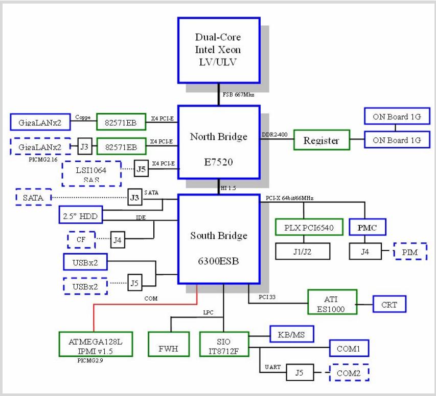
cPCI-6910 with cPCI-R6910 Block Diagram
![The flowchart depicts a computer motherboard architecture centered around Intel processors and bridges.\n\n**Central Components:**\n*   **Dual-Core Intel Xeon LV/ULV** connects via **FSB 667Mhz** to the **North Bridge E7520**.\n*   The **North Bridge E7520** connects via **HI 1.5** to the **South Bridge 6300ESB**.\n\n**North Bridge E7520 Connections:**\n*   **X4 PCI-E** connects to **82571EB**, which connects to **GigaLANx2** (label: **Copper**).\n*   **X4 PCI-E** connects to another **82571EB**, which connects to **J3** (located inside a dashed box labeled **GigaLANx2 PICMG2.16**).\n*   **X4 PCI-E** connects to **J5**, which connects to **LSI1064 SAS**.\n*   **DDR2-400** connects to **Register**, which connects to two stacked blocks labeled **ON Board 1G**.\n\n**South Bridge 6300ESB Connections:**\n*   **J3** connects to **2.5' HDD** via **IDE**. A dotted line from a dashed box labeled **SATA** points to **J3** (label: **S ATA**).\n*   **J4** connects to **CF**.\n*   **J5** connects to **USBx2**. A dashed box labeled **USBx2** also connects to **J5**.\n*   A red line labeled **COM** connects to **ATMEGA128L IPMI v1.5** (label: **PICMG2.9**).\n*   **PCI-X 64bit@66MHz** connects to a bus splitting into **PLX PCI6540** and **PMC**.\n    *   **PLX PCI6540** connects to **J1/J2**.\n    *   **PMC** connects to **J4**, which connects to a dashed box labeled **PIM**.\n*   **PCI 13** connects to **ATI ES1000**, which connects to **CRT**.\n*   **LPC** connects to **FWH** and **SIO IT8712F**.\n    *   **SIO IT8712F** connects to **KB/MS** and **UART**.\n    *   **KB/MS** connects to **COM1**.\n    *   **UART** connects to **J5**, which connects to a dashed box labeled **COM2**.](.cpci-6910-manual-13/5049fc41ae706e454fde5ae1bc4226e1b7b27178d198dca27b6b3b155f402abe.jpg)

Figure 1-1: cPCI-6910 with cPCI-R6910 Block Diagram

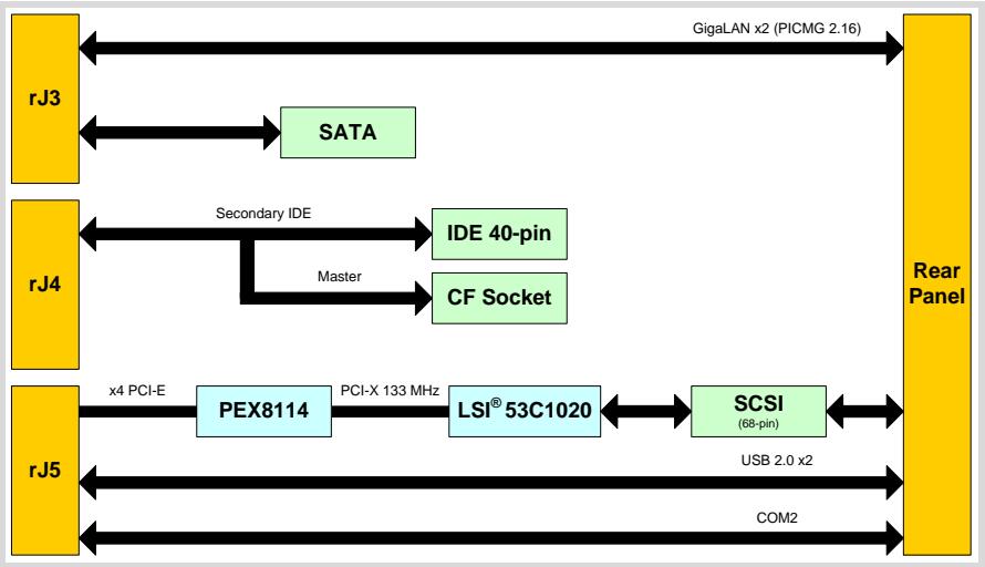
cPCI-R6911 Block Diagram
![Based on the provided flowchart, here are the labeled blocks and their connections:\n\n**Labeled Blocks:**\n*   **rJ3** (Yellow block)\n*   **SATA** (Green block)\n*   **rJ4** (Yellow block)\n*   **IDE 40-pin** (Green block)\n*   **CF Socket** (Green block)\n*   **rJ5** (Yellow block)\n*   **PEX8114** (Blue block)\n*   **LSI® 53C1020** (Blue block)\n*   **SCSI (68-pin)** (Green block)\n*   **Rear Panel** (Yellow block)\n\n**Connections:**\n*   **rJ3** connects bidirectionally to **Rear Panel** via a link labeled 'GigaLAN x2 (PICMG 2.16)'.\n*   **rJ3** connects bidirectionally to **SATA**.\n*   **rJ4** connects to **IDE 40-pin** via a path labeled 'Secondary IDE'.\n*   **rJ4** connects to **CF Socket** via a branch labeled 'Master'.\n*   **rJ5** connects to **PEX8114** via a link labeled 'x4 PCI-E'.\n*   **PEX8114** connects to **LSI® 53C1020** via a link labeled 'PCI-X 133 MHz'.\n*   **LSI® 53C1020** connects bidirectionally to **SCSI (68-pin)**.\n*   **SCSI (68-pin)** connects bidirectionally to **Rear Panel**.\n*   **rJ5** connects bidirectionally to **Rear Panel** via a link labeled 'USB 2.0 x2'.\n*   **rJ5** connects bidirectionally to **Rear Panel** via a link labeled 'COM2'.](.cpci-6910-manual-13/6e89776307ebece773bfed14e3875d60f8bf7f349f53466ede6b9decbea52363.jpg)

Figure 1-2: cPCI-R6911 Block Diagram

# 1.3 Product List

The cPCI-6910 Series SBS and supported rear transition modules come in the following configurations.

# cPCI-6910 Configurations

▶ cPCI-6910/DCX20/M1G

Dual-Core Intel $^{®}$ Xeon $^{®}$ Processor LV 2.0 GHz with 1 GB soldered memory. Ports: COM1, PS/2, VGA, 2 x USB, 2 x GbE, PMC. Storage: IDE/SATA/CF (optional)

▶ cPCI-6910/DCX20/M2G

Dual-Core Intel $^{®}$ Xeon $^{®}$ Processor LV 2.0 GHz with 2 GB soldered memory. Ports: COM1, PS/2, VGA, 2 x USB, 2 x GbE, PMC. Storage: IDE/SATA/CF (optional)

▶ cPCI-6910/DCX16/M1G

Dual-Core Intel $^{®}$ Xeon $^{®}$ Processor ULV 1.66 GHz with 1 GB soldered memory. Ports: COM1, PS/2, VGA, 2 x USB, 2 x GbE, PMC. Storage: IDE/SATA/CF (optional)

▶ cPCI-6910/DCX16/M2G

Dual-Core Intel $^{®}$ Xeon $^{®}$ Processor ULV 1.66 GHz with 2 GB soldered memory. Ports: COM1, PS/2, VGA, 2 x USB, 2 x GbE, PMC. Storage: IDE/SATA/CF (optional)

▶ cPCI-6910/DXL16/M1G

Dual-Core Intel $^{®}$ Xeon $^{®}$ Processor LV 1.66 GHz with 1 GB soldered memory. Ports: COM1, PS/2, VGA, 2 x USB, 2 x GbE, PMC. Storage: IDE/SATA/CF (optional)

▶ cPCI-6910/DXL16/M2G

Dual-Core Intel $^{®}$ Xeon $^{®}$ Processor LV 1.66 GHz with 2 GB soldered memory. Ports: COM1, PS/2, VGA, 2 x USB, 2 x GbE, PMC. Storage: IDE/SATA/CF (optional)

# Rear Transition Modules

▶ cPCI-R6910

2 x GbE, 2 x USB, COM2, CF card slot, and SAS/SATA connector

▶ cPCI-R6911

2 x GbE, 2 x USB, COM2, SATA, IDE, CF card slot, and SCSI connector

# 1.4 Package Contents

Before unpacking, check the shipping carton for any damage. If the shipping carton and/or contents are damaged, inform your dealer immediately. Retain the shipping carton and packing materials for inspection. Obtain authorization from your dealer before returning any product to ADLINK.

Check if the following items are included in the package.

# CPU Module

▶ cPCI-6910 single board computer
▶ 2.5" SATA HDD accessory pack (including one DB-6910SAT removable SATA socket adapter and screws)
▶ 2.5" IDE HDD accessory pack (including one DB-6910IDE removable IDE socket adapter and screws)
Heatsink kit
▶ RJ-45-DB9 cable
▶ Y-cable for PS/2 combo port
▶ ADLINK All-in-One driver CD
▶ User's manual

# Rear Transition Module (RTM)

▶ cPCI-R6910/cPCI-R6911 RTM
▶ 2.5" SATA HDD accessory pack including one DB-R6910SAT and screws (cPCI-R6910 only)
▶ 2.5" SAS HDD accessory pack including one DB-R6910SAS and screws (cPCI-R6910 only)
▶ SATA HDD signal and power cables (cPCI-R6911 only)
▶ Ultra-320 SCSI cable (cPCI-R6911 only)

# Optional Components

▶ CompactFlash $^{®}$ adapter accessory pack, including DB-6910CF removable CF socket adapter and screws

<table><tr><td>NOTES:</td><td>CPU, memory, and HDD specifications may vary depending on the selected SBC configuration.</td></tr><tr><td></td><td>The HDD accessory pack is not available when the 2.5&quot; HDD is pre-installed.</td></tr><tr><td></td><td>The heatsink kit is not included when the CPU is pre-installed.</td></tr><tr><td></td><td>The contents of non-standard cPCI-6910 configurations may vary depending on customer requirements.</td></tr></table>

<table><tr><td>CAUTION:</td><td>This product must be protected from static discharge and physical shock. Never remove any of the components except at a static-free workstation. Use the anti-static bag shipped with the product when putting the board on a surface. Wear an anti-static wrist strap properly grounded on one of the system&#x27;s ESD ground jacks when installing or servicing system components.</td></tr></table>

This page intentionally left blank.

# 2 Specifications

This section tells you the specifications of the SBC and supported rear transition modules.

# 2.1 cPCI-6910 SBC Specifications

<table><tr><td>CompactPCI®Standards</td><td>PICMG®2.0 CompactPCI®Rev. 3.0PICMG®2.1 CompactPCI®hot-swap specification Rev. 2.0PICMG®2.9 System Management Bus Rev. 1.0 (IPMI v1.5)PICMG®2.16 Packet Switching Backplane Rev.1.0</td></tr><tr><td>Form Factor</td><td>Standard 6U CompactPCI®Board size: 233.35 mm x 160 mmOne slot width (4HP, 20.32 mm)</td></tr><tr><td>CPU</td><td>Single processor on 478-pin micro FCPGA socketDual-Core Intel®Xeon®Processor LV, 2.0 GHz, Dual-Core Intel®Xeon®Processor LV, 1.66 GHz or Dual-Core Intel®Xeon®Processor ULV, 1.66 GHz set in 65 nm process technology2 MB on die L2 cache, 677 MHz FSB</td></tr><tr><td>Chipset</td><td>Intel®E7520 Memory Controller Hub (GMCH)Intel®6300ESB I/O Hub</td></tr><tr><td>Host Memory</td><td>2 GB or 1 GB soldered system memoryDDR2 400 MHz registered SDRAM with ECC</td></tr><tr><td>CompactPCI®Bus</td><td>64-bit/66 MHz CompactPCI®BusPLX PCI-6540 64-bit/66 MHz PCI-X to PCI-X Bridge</td></tr><tr><td>Graphics</td><td>ATI ES1000 controller on PCI 32-bit/33 MHz busUp to 250 MHz graphics memory2D graphics accelerator</td></tr><tr><td>Gigabit Ethernet</td><td>Up to four gigabit Ethernet ports, two in front and 2 on rear panelTwo Intel®82546EB Ethernet controller, based on PCI Express®x4 bus connected to J3 for Packet Switched Backplane (PSB)</td></tr><tr><td>IDE</td><td>Dual-channel IDE44-pin primary IDE connector for onboard HDD and secondary connector on rear via J4 connectorBus Master IDE controller supports two UltraATA 100/66/33 devices</td></tr><tr><td>BIOS $^{1}$ </td><td>Award-Phoenix with 4 MB Flash ROMBIOS write protection featureBoot from USB storage devices including USB-Floppy, USB-ZIP, USB-CD-ROM, and USB-HDDSupports Desktop Management Interface (DMI)Supports Enhanced Intel SpeedStep $^{\textregistered}$  technologySupports optional OEM BIOS features</td></tr><tr><td>IPMI Interface</td><td>Supports PICMG $^{\textregistered}$  2.9 secondary system managing busImplements IPMI functions defined by IPMI Specification v1.5ATmega128L-8AU Baseboard Management Controller (BMC) with 128 KB programmable In-System Flash, 4 KB EEPROM, and 4 KB internal SDRAM</td></tr><tr><td>Faceplate I/O Ports</td><td>COM1 (RS-232)PS/2 keyboard and mouse combo portVGA (DB-9)2 x USB 2.02 x gigabit Ethernet ports (RJ-45)</td></tr><tr><td>Onboard Peripherals $^{2}$ </td><td>44-pin IDE connectorSerial ATA connectorCompactFlash $^{\textregistered}$  connector</td></tr><tr><td>OS Compatibility</td><td>Windows $^{\textregistered}$  2000Windows $^{\textregistered}$  XPWindows $^{\textregistered}$  Server 2003Red Hat Fedora Core 6Other OS supported upon request</td></tr><tr><td>Environment</td><td>Operating temperature $^{3}$ :Intel® Xeon® LV CPU: -10 °C to 50 °CIntel® Xeon® ULV CPU: -10 °C to 70 °CStorage temperature: -40 °C to 85 °CHumidity: 5% to 95% non-condensingShock: 15G peak-to-peak, 11ms duration,non-operationVibration $^{4}$ :Non-operation: 1.88 Grms, 5 Hz to 500 Hz, eachaxisOperation: 0.5 Grms, 5 Hz to 500 Hz, each axis</td></tr><tr><td>Safety Certificates and Tests</td><td>CE/FCC Class A</td></tr></table>

1. Due to BIOS segment limitations, enabling the remote console function may occupy the same memory space as other ROM mapping add-on or boot-up devices including Pre-boot Agent of Ethernet Boot ROM, SCSI Boot ROM, or add-on EIDE Boot ROM. It is recommended that you enable only one ROM-mapping add-on or boot-up device when enabling the remote console function.
2. The IDE HDD/Serial ATA HDD/CompactFlash card connector comes in an adapter design. These are removable and should not be used/connected simultaneously. The 2.5" HDD space is reserved.
3. ADLINK-certified thermal design. The thermal performance is dependent on the chassis cooling design. Forced airflow with 30 CFM is required. Temperature limit of optional mass storage devices may affect the thermal specification.
4. The HDD limits the operational vibration. When application requires higher definition for anti-vibration, it is recommended that you use a flash disk.

Specifications are subject to change without prior notice.

# 2.2 cPCI-R6910/cPCI-R6911 RTM Specifications

<table><tr><td>Form Factor</td><td>Standard 6U CompactPCI® rear I/OBoard size: 233.35 mm x 80 mmOne slot width (4HP, 20.32 mm)CompactPCI® connectors: with rJ3, rJ4 and rJ5 connectors</td></tr><tr><td>Faceplate I/O Connectors</td><td>COM2 (RS-232)2 x gigabit Ethernet ports2 x USB 2.0 ports68-pin SCSI socket (cPCI-R6911 only)</td></tr><tr><td>Onboard Peripherals</td><td>CompactFlash® Type II card slotSerial Attached SCSI connector1 (cPCI-R6910 only)Serial ATA connector (cPCI-R6910 only)40-pin IDE connector2 (cPCI-R6911 only)68-pin SCSI connector (cPCI-R6911 only)</td></tr><tr><td>SCSI (cPCI-R6911 only)</td><td>LSI® Logic LSI53C1020 PCI-X Ultra320 SCSI Controller Integrated RAIDTM on PCI-X 64-bit/133 MHz bus320 MB per second data transfer rateSupports RAIDTM 0 (striping) and RAIDTM 1/1E (mirroring)</td></tr></table>

1. The Serial Attached SCSI and Serial ATA HDD connectors come in a removable adapter design. These should not be used/connected simultaneously. The 2.5" HDD space is reserved.
2. When using the CompactFlash card slot, the 40-pin IDE connector supports only one IDE device.

Specifications are subject to change without prior notice.

# 2.3 I/O Connectivity Table

<table><tr><td rowspan="2">I/O</td><td colspan="2">cPCI-6910</td><td colspan="2">cPCI-R6910 RTM</td><td colspan="2">cPCI-R6911 RTM</td></tr><tr><td>Faceplate</td><td>Onboard</td><td>Faceplate</td><td>Onboard</td><td>Faceplate</td><td>Onboard</td></tr><tr><td>Serial Port</td><td>Y</td><td>--</td><td>Y(J5)</td><td>--</td><td>Y(J5)</td><td>--</td></tr><tr><td>USB</td><td>Yx2</td><td>--</td><td>Y(J5) x2</td><td>--</td><td>Y(J5) x2</td><td>--</td></tr><tr><td>Gigabit Ethernet</td><td>Yx2</td><td>--</td><td>Y(J3) x2</td><td>--</td><td>Y(J3) x2</td><td>--</td></tr><tr><td>SCSI</td><td></td><td></td><td></td><td>--</td><td>Y(J3)</td><td>Y(J3)</td></tr><tr><td>PS2 Keyboard/Mouse</td><td>Y</td><td>--</td><td>--</td><td>--</td><td>--</td><td>--</td></tr><tr><td>VGA</td><td>Y</td><td>--</td><td>--</td><td>--</td><td>--</td><td>--</td></tr><tr><td>IDE</td><td>--</td><td>Y (44-pin)*</td><td>--</td><td>--</td><td>--</td><td>Y(J4, 40-pin)</td></tr><tr><td>CompactFlash®</td><td>--</td><td>Y*</td><td>--</td><td>Y</td><td>--</td><td>Y</td></tr><tr><td>SATA</td><td>--</td><td>Y*</td><td>--</td><td>Y(J5)*</td><td>--</td><td>Y(J5)</td></tr><tr><td>SAS</td><td>--</td><td>--</td><td>Y(J5)*</td><td>--</td><td>--</td><td>--</td></tr><tr><td>PMC</td><td>Y</td><td>--</td><td>--</td><td>--</td><td>--</td><td>--</td></tr><tr><td>General Purpose LED</td><td>Y</td><td>--</td><td>--</td><td>--</td><td>--</td><td>--</td></tr><tr><td>Reset button</td><td>Y</td><td>--</td><td>--</td><td>--</td><td>--</td><td>--</td></tr></table>

\* Removable adapter design

# 2.4 Power Consumption

This section provides information on the power consumption of cPCI-6910 when using Dual-Core Intel $^{®}$ Xeon $^{®}$ ULV Processor at 1.66 GHz and a Dual-Core Intel $^{®}$ Xeon $^{®}$ LV Processor at 2.0 GHz. The cPCI-6910 was tested under the following environment:

<table><tr><td>Operating system</td><td>DOS, Linux®, Windows® XP</td></tr><tr><td>System memory</td><td>2 GB DDR2-400 registered SDRAM with ECC</td></tr><tr><td>Storage</td><td>Seagate Momentus 5400 X2 SATA 1.5 Gb/s 80 GB HDD</td></tr><tr><td>Program</td><td>Intel® Sossaman Maximum Power Program Rev. 2.0</td></tr><tr><td>Backplane</td><td>ADLINK cBP-6105R Rev.A2</td></tr><tr><td>Power Supply</td><td>Seventeam ST-350HLP 350W</td></tr></table>

The following tables show the cPCI power consumption during idle mode (no application is running) and full loading (100% CPU usage).

Idle mode under DOS

<table><tr><td rowspan="3">Voltage (V)</td><td colspan="6">CPU</td></tr><tr><td colspan="2">ULV 1.66 GHz</td><td colspan="2">LV 2.0 GHz</td><td colspan="2">LV 1.66 GHz</td></tr><tr><td>Current (A)</td><td>Power (watts)</td><td>Current (A)</td><td>Power (watts)</td><td>Current (A)</td><td>Power (watts)</td></tr><tr><td>5</td><td>4.5</td><td>22.5</td><td>5.7</td><td>28.5</td><td>5.1</td><td>25.5</td></tr><tr><td>3.3</td><td>1.5</td><td>5.0</td><td>1.5</td><td>5.0</td><td>1.49</td><td>4.92</td></tr><tr><td>Total</td><td></td><td>27.5</td><td></td><td>33.5</td><td></td><td>30.4</td></tr></table>

Idle mode under Linux®

<table><tr><td rowspan="3">Voltage (V)</td><td colspan="6">CPU</td></tr><tr><td colspan="2">ULV 1.66 GHz</td><td colspan="2">LV 2.0 GHz</td><td colspan="2">LV 1.66 GHz</td></tr><tr><td>Current (A)</td><td>Power (watts)</td><td>Current (A)</td><td>Power (watts)</td><td>Current (A)</td><td>Power (watts)</td></tr><tr><td>5</td><td>3.9</td><td>19.5</td><td>4.4</td><td>22.0</td><td>4.2</td><td>2.1</td></tr><tr><td>3.3</td><td>1.6</td><td>5.3</td><td>1.7</td><td>5.6</td><td>1.6</td><td>5.3</td></tr><tr><td>Total</td><td></td><td>24.8</td><td></td><td>27.6</td><td></td><td>26.3</td></tr></table>

Full-load CPU mode under Windows $^{®}$ XP

<table><tr><td rowspan="3">Voltage (V)</td><td colspan="6">CPU</td></tr><tr><td colspan="2">ULV 1.66 GHz</td><td colspan="2">LV 2.0 GHz</td><td colspan="2">LV 1.66 GHz</td></tr><tr><td>Current (A)</td><td>Power (watts)</td><td>Current (A)</td><td>Power (watts)</td><td>Current (A)</td><td>Power (watts)</td></tr><tr><td>5</td><td>6.9</td><td>34.5</td><td>8.7</td><td>43.5</td><td>7.6</td><td>38</td></tr><tr><td>3.3</td><td>1.5</td><td>5.0</td><td>1.55</td><td>5.0</td><td>1.55</td><td>5.1</td></tr><tr><td>Total</td><td></td><td>39.5</td><td></td><td>48.5</td><td></td><td>43.1</td></tr></table>

Idle mode under Windows® XP

<table><tr><td rowspan="3">Voltage (V)</td><td colspan="6">CPU</td></tr><tr><td colspan="2">ULV 1.66 GHz</td><td colspan="2">LV 2.0 GHz</td><td colspan="2">LV 1.66 GHz</td></tr><tr><td>Current (A)</td><td>Power (watts)</td><td>Current (A)</td><td>Power (watts)</td><td>Current (A)</td><td>Power (watts)</td></tr><tr><td>5</td><td>3.9</td><td>19.5</td><td>4.1</td><td>20.5</td><td>4.2</td><td>21.0</td></tr><tr><td>3.3</td><td>1.5</td><td>5.0</td><td>1.6</td><td>5.3</td><td>1.5</td><td>5.0</td></tr><tr><td>Total</td><td></td><td>24.5</td><td></td><td>25.8</td><td></td><td>26.0</td></tr></table>

This page intentionally left blank.

# 3 Functional Description

The following sections describe the cPCI-6910 features and functions.

# 3.1 Processor

The cPCI-6910 supports a Dual-Core Intel $^{®}$ Xeon $^{®}$ processor LV/ULV (2.0 GHz/1.66 GHz) with 2 MB L2 cache in a micro-FCPGA package. The Dual-Core Intel $^{®}$ Xeon $^{®}$ processor LV/ULV is a high-performance, low-power consuming processor with several micro-architectural enhancements over existing Intel processors, including:

▶ Chip Multi-Processing (CMP)-based architecture (dualcores on chip)
▶ Optimized for best MPS/Watt with CMP-enabled software
▶ Advanced pre-fetching mechanisms
▶ Advanced power management and throttling mechanisms

# 3.2 Chipset

The cPCI-6910 incorporates the Intel $^{®}$ E7520 chipset consisting of three PCI Express $^{®}$ x8 channels, Memory Controller Hub, and I/O Controller Hub (Intel $^{®}$ 6300ESB).

The Intel $^{®}$ E7520 comes with a memory controller hub component for embedded platforms. It also provides the processor, DDR2 system memory, hub, and PCI Express $^{®}$ interfaces.

# 3.3 Memory

The cPCI-6910 comes with a dual-channel DDR2 system memory architecture that supports x72, buffered, registered DDR2 400 MHz SDRAM with ECC. The Intel $^{®}$ E7520 supports 1 GB/512 MB memory with error checking and correcting (ECC) mechanism provided by Chipkill technology on x8 DIMMS to ensure data and memory integrity. The Intel $^{®}$ E7520 memory interface supports the following:

▶ Direct connection of two memory channel interfaces with DDR2 400 DIMMs
▶ Full operational support in single-channel mode on either channel interface. Lock-step support only for dual-channel operation (logically shared address, independent data)
▶ Stacked or unstacked DIMM support for registered DDR2-400 DIMMs
▶ 144-bit wide with ECC slot supports x72, registered DDR2 400 DIMMs in 256 MB/512 MB/1 GB package
▶ Maximum 16 GB support with DDR2 400 up to two stacked DIMMs (1 GB x 4 DRAMs)
▶ Base DDR2 clock rates of up to 200 MHz
▶ Data interface double-pumped to 400 MHz
▶ Up to 3.2 GB/s (DDR2 400) data bandwidth per channel
▶ S4EC/D4ED (144, 128) x 4, Intel $^{®}$ x4 Signal Device Data Correction (x4 SDDC) ECC in dual-channel mode
▶ SEC/DED (72, 64) ECC on each channel when Intel® Signal Device Data Correction (SDDC) is disable
▶ 14-bit address bus
▶ RASUM fail-over to an on-line spare DIMM device
▶ Hardware refresh support for 100 MHz operation to facilitate debug frequencies
▶ Memory mirroring
▶ ODT (on-die termination) for DDR2 400
▶ Four-channel DMA controller for embedded applications.

<table><tr><td>NOTE</td><td>Refer to the Intel® E7520 Memory Controller Hub (MCH) DMA Application Note. For additional details, contact your local Intel field representative.</td></tr></table>

# 3.4 PCI Express $^{®}$ (High-speed Serial I/O)

- Three x8 port configuration interfaces, with each interface supporting connection to PCI, Ethernet, iSCSI devices (6700PXH, 82571EB Gigabit Ethernet Controller, or I/O processor), or other PCI Express $^{\textregistered}$ peripherals
▶ Each x8 interface is capable of logically dividing into separate x4 interfaces, with half the bandwidth of x8 interface and fully compliant with x4 specifications
▶ Simultaneous 2.5 Gb/s (each direction, 5 Gb/s per port) maximum theoretical peak bandwidth for every x8 PCI Express interface
▶ Simultaneous 1.25 Gb/s (each direction, 2.5 Gb/s per port) maximum theoretical peak bandwidth for every x4 PCI Express® interface
▶ Automatic wake-up and training of PCI Express $^{®}$ ports out of reset
▶ 32-bit CRC on all transaction layer packets with link-level retry on error (recovery from transient errors without software visible system failure)
▶ 16-bit CRC on all link message information
▶ Hardware detection hot-plug support at the PCI Express $^{®}$ link level above and beyond the PCI hot-plug support provided by the 6700PXH or any equivalent bridge

# 3.5 Hub Interface 1.5

▶ 266 MB/s Point-to-Point Connection for Intel $^{®}$ 6300ESB with parity protection
▶ 8-bit wide, 66 MHz base clock, 4X data transfer
▶ Parallel termination mode for longer trace length
▶ Upstream hub interface for Intel® E7520 access

# 3.6 Intel $^{®}$ 6300ESB I/O Controller Hub (ICH)

The cPCI-6910 features a highly-integrated, multi-functional I/O Controller Hub (ICH) that supports the interface to the PCI bus, and various I/O functions for current and legacy devices. The chipset communicates via a dedicated hub interface (HI-1.5). The Intel $^{®}$ 6300ESB functions and features include:

▶ Upstream hub interface for Intel® E7520 access
▶ 2-port Serial ATA controller
▶ 2-channel Ultra ATA/100 Bus Master IDE controller
▶ EHCI USB 2.0 host controller and two UHCI USB 1.1 host controller (supporting up to 4 USB ports)
▶ I/O APIC
▶ SMBus 2.0 controller
▶ FWH interface
▶ LPC interface
▶ AC'97 2.2 interface
▶ PCI-X 1.0 interface
▶ PCI 2.2 interface
▶ Two serial I/O ports
▶ 2-stage watchdog timer

The Intel $^{®}$ 6300ESB also comes with the necessary arbitration and buffering to ensure efficient utilization of supported interfaces.

# NOTE

For Intel $^{®}$ 6300ESB design and layout information, refer to the Intel $^{®}$ 6300ESB I/O Controller Hub Design Guide.

# 3.7 Ultra ATA100/66/33 IDE

The cPCI-6910 supports dual-channel Ultra ATA100 IDE. The primary IDE channel comes onboard the cPCI-6910, while the secondary IDE is routed to the rear transition module (cPCI-R6910) via the J4 connectors. 2.5" hard disk drive slots may be used for the primary IDE interfaces. The Intel® 6300ESB IDE controller supports both legacy and native IDE interface modes. In native mode, the IDE controller functions as a PCI-compliant software interface and does not use any legacy I/O or interrupt resources. For Ultra ATA100/66 modes, proper IDE cables must be used.

# 3.8 USB 2.0

The cPCI-6910 comes with two EHCI USB 2.0 Host Controllers (shared with UHCI ports) for up to two USB ports on the front panel. The Intel $^{®}$ 6300ESB host controllers support the standard Universal Host Controller Interface (UHCI) Design Guide and over-current detection on all USB ports. Legacy USB devices, such as keyboard, mouse, and floppy disk drives are supported and may be enabled or disabled in the BIOS. Booting the system from a USB floppy disk drive is implemented on all USB ports.

# 3.9 LPC/Firmware Hub

The 4 Mb system BIOS flash—SST 49LF004A—is compatible with Intel 82802 Firmware Hub (FWH) device specifications. The BIOS is shielded by a write-protect function that can be enabled or disabled in the BIOS option menu.

# 3.10 System Management Bus

The Intel $^{®}$ 6300ESB comes with a System Management Bus (SMBus) that is compliant with SMBus Specification Version 2.0. The host controller provides a mechanism for the processor to initiate communications with SMBus peripherals (slaves) as well as I2C-compatible devices. The Slave Interface allows an external master to read from or write to the Intel $^{®}$ 6300ESB.

# 3.11 UART

The serial port has a UART that supports all functions of a standard 16550 UART including hardware flow control interface. The UART performs serial-to-parallel conversion of data characters received from a peripheral device or a modem and parallel-to-serial conversion of data characters received from the processor.

# 3.12 Watchdog Timer

The cPCI-6910 implements a 2-stage watchdog timer (WDT). The WDT is embedded in the Intel® 6300ESB and may be enabled or disabled through the BIOS. The WDT supports selectable pres-clear that is approximately 1 MHz (1 us to 1 s) and approximately 1 KHz (1 ms to 10 min). When the programmed time is up, the WDT generates an IRQ, SMI, or SCI interrupt, then drives the ICH\_WDT-L low, and resets the cPCI-6910.

# 3.13 Real Time Clock

The Real Time Clock (RTC) module provides a battery backed-up date and time keeping device with two banks of 128-byte static RAM. The design is functionally compatible with the Motorola MS146818. The time keeping comes from a 32.768 KHz oscillating source, that is divided to achieve an update every second.

# 3.14 PCI 32-bit and PCI-X Interface

The Intel $^{®}$ 6300ESB supports one 32-bit/33 MHz PCI interface compliant with PCI Local Bus Specification Revision 2.2. With a 120 MB/s throughput, this bus supports 44-bit addressing using DAC protocol. The cPCI-6910 uses this bus to implement the VGA interface (ATI RS 1000 chip), one PMC port, and one PCI to PCI bridge in PCI-X bus.

# 3.15 ATI ES1000 VGA chip

▶ Maximum 2D performance with the fastest available 2D graphics for multimedia applications in true 24-bit color
▶ Comprehensive support for Windows $^{®}$ Server OS, including GDI extension acceleration like Alpha BLTs and Gradient Fills, as well as exclusive alpha cursor support

# 3.16 Hardware Monitor

The IT8712F monitors critical hardware parameters including system and CPU voltages and temperatures. All hardware health status may be accessed in the BIOS and run-time utilities. In addition, once the preset thresholds of hardware conditions are reached, the W83627HF chip alerts or resets the system.

# 3.17 PCI Resource Allocation

The cPCI-6910 comes with a 133 MHz PCI bus. The IDSEL, INT#, and REQ#/GNT# routines of the cPCI bus slots on the backplane follow standard definitions with the Intel® 6300ESB as the interrupt controller. The table below shows the cPCI-6910 PCI resource allocation.

<table><tr><td>Function</td><td>REQ</td><td>GNT</td><td>IDSEL</td><td>INTA</td><td>INTB</td><td>INTC</td><td>INTD</td></tr><tr><td>PXL PCI-6540</td><td>PCIX_REQ-L0</td><td>PCIX_GNT-L0</td><td>PCIX_AD20</td><td>PCIX_IRQ-L0</td><td></td><td></td><td></td></tr><tr><td>PMC</td><td>PCIX_REQ-L1</td><td>PCIX_GNT-L1</td><td>PCIX_AD22</td><td></td><td>PCIX_IRQB-L1</td><td></td><td></td></tr><tr><td>J1</td><td></td><td></td><td></td><td>PCIX_IRQ-L0</td><td>PCIX_IRQ-L1</td><td>PCIX_IRQ-L2</td><td>PCIX_IRQ-L3</td></tr><tr><td>ATI ES1000</td><td>PCI_REQ-L0</td><td>PCI_GNT-L0</td><td>PCI_AD18</td><td>PCI_IRQ-L0</td><td></td><td></td><td></td></tr></table>

# 3.18 PCI-X to PCI-X Bridge

The PLX FastLane™ PCI-6540 is a dual-mode universal PCI-X-to-PCI-X bridge and implements the system/peripheral slot on the cPCI-6910. The dual-mode device is capable of operating in transparent, non-transparent, or universal mode. When in non-transparent mode, the cPCI-6910 permits independent memory mapping of both primary and secondary bus with powerful configuration options to support intelligent subsystems. The universal mode permits jumper-less configuration between applications to CompactPCI® interface at peripheral and/or system slot. The universal mode option enables configuration of the PCI-6540 bridge as a transparent bridge in a system slot supporting a host, or as a non-transparent bridge in a peripheral slot as an intelligent subsystem. These options allow installation of the cPCI-6910 in both peripheral and/or system slots.

# 4 Jumpers and Connectors

This chapter illustrates the board layout, connector pin assignments, and jumper settings to familiarize the users on the cPCI-6910.

4.1 cPCI-6910 Board Layout
![162.53\n233,2 ±0.15](.cpci-6910-manual-13/38378ffd1411891dbd0ef4970faf1dd815b489c1976bcfb7cd14297c32ed0d67.jpg)

<table><tr><td>A</td><td>CPU Socket</td><td>J</td><td>Buzzer</td></tr><tr><td>B</td><td>Intel® E7520</td><td>K</td><td>Soldered memory chips</td></tr><tr><td>C</td><td>PLX PCI-6540</td><td>L</td><td>PMC socket</td></tr><tr><td>D</td><td>Intel® 6300ESB</td><td>M</td><td>cPCI-J1</td></tr><tr><td>E</td><td>ATI ES1000</td><td>N</td><td>cPCI-J2</td></tr><tr><td>F</td><td>Intel® 82571EB</td><td>O</td><td>cPCI-J3</td></tr><tr><td>G</td><td>SIO (IT8217F)</td><td>P</td><td>cPCI-J4</td></tr><tr><td>H</td><td>BIOS</td><td>Q</td><td>cPCI-J5</td></tr><tr><td>I</td><td>RTC Battery</td><td>R</td><td>Board-to-board connector</td></tr></table>

# 4.2 cPCI-6910 Front Panel

![PMC\nGGE2 GGE1 COM\nUSB KB/MS VGA\nI/O port\nA B C D E F G](.cpci-6910-manual-13/05b4e841b13303f9d71eec501f3f148476cb1e270078b090db3c84153113757a.jpg)

<table><tr><td>A</td><td>PMC slot</td></tr><tr><td>B</td><td>Gigabit Ethernet Port 1/2</td></tr><tr><td>C</td><td>COM1 port</td></tr><tr><td>D</td><td>USB 2.0 ports</td></tr><tr><td>E</td><td>KB/MS port</td></tr><tr><td>F</td><td>VGA port</td></tr><tr><td>G</td><td>System LEDs and reset button</td></tr></table>

# System LED indication

![HD WDT\nPW GP\nRST](.cpci-6910-manual-13/9e458bd30384854c24b758f98f937e4c9c704c378ef466050d4c3a9f95bc6b99.jpg)

<table><tr><td>LED</td><td>Color</td><td>Condition</td><td>Indication</td></tr><tr><td rowspan="3">HDD</td><td rowspan="3">Red</td><td>OFF</td><td>No HDD</td></tr><tr><td>ON</td><td>HDD is installed</td></tr><tr><td>Blinking</td><td>Data read/write in process</td></tr><tr><td rowspan="2">Power</td><td rowspan="2">Yellow</td><td>OFF</td><td>System is off</td></tr><tr><td>ON</td><td>System in on</td></tr><tr><td rowspan="2">Watchdog</td><td rowspan="2">Amber</td><td>OFF</td><td>Watchdog event de-alert</td></tr><tr><td>ON</td><td>Watchdog event alert</td></tr><tr><td rowspan="2">Hotswap</td><td rowspan="2">Blue</td><td>OFF</td><td>Handler is close/System is on</td></tr><tr><td>ON</td><td>Handler is open</td></tr></table>

# 4.3 cPCI-6910 Daughterboard Layout

DB-6910IDE
![Pure electrical connector pinout diagram without any text or symbols](.cpci-6910-manual-13/6f9832c78567c88d4573e313ee7be6c27b169b657802e6e2ca1f824b84f12b87.jpg)

44-pin IDE connector
Front view

![Diagram of a dual-chamber connector with pin layout and mounting holes (no text or labels)](.cpci-6910-manual-13/0ca4e1667f7b7bafa2e6f866bbe6252dd5e58476363759aaf953d4e965386423.jpg)

Board to board connector
Rear View

DB-6910SAT
![Pure electrical connector diagram without any text, numbers, or symbols](.cpci-6910-manual-13/69cc33a09a45489f5f8c0a55034340792f1bd3b73ff7f201cf4f1a7dadd63bee.jpg)

SATA connector
Front view

![Pure electrical connector diagram without any text, numbers, or symbols](.cpci-6910-manual-13/755175fbdfe2fed240c9679f99d832b9d43a2b8e0bd77c0f3b5e9aff0419ce00.jpg)

Board to board connector
Rear View

DB-6910CF
![Pure electrical circuit lines without any symbols](.cpci-6910-manual-13/98b588b3607545faa5e1e24b2d31bd9fd9e905adbcbb7935a1bfa465d12a23b2.jpg)

CompactFlash socket
Front view

![Pure electrical circuit lines without any symbols](.cpci-6910-manual-13/63463f89ea35e3f610fbfc215910bbf269c12d857acf4513fdf81627e624f8e9.jpg)

Board to board connector
Rear View

# 4.4 Rear Transition Modules

cPCI-R6910 Board and Daughterboard Layouts
![82.53\n233.2±0.15\nG D\nF C\nB H\nE A\nCOM port\nUSB ports\nGbE4 port\nGbE3 port](.cpci-6910-manual-13/aae2baddcdf23698890e9f3690bc7556b04abe29c0d8f7d4cc874d061f409ac2.jpg)

<table><tr><td>A</td><td>Board to board connector</td><td>E</td><td>cPCI rJ3 connector</td></tr><tr><td>B</td><td>SAS nVRAM</td><td>F</td><td>cPCI rJ4 connector</td></tr><tr><td>C</td><td>LSI1064E controller</td><td>G</td><td>cPCI rJ5 connector</td></tr><tr><td>D</td><td>CompactFlash® socket</td><td>H</td><td>SAS Flash ROM</td></tr></table>

# DB-R6910SAS

![Board to board connector\nSAS connector\nRear view](.cpci-6910-manual-13/eb28d0ea687d1ae6b3de57f46ebe3635af78b2ed0ffbe42cec575f8e9b1d262b.jpg)

# DB-R6910SAT

![Pure electrical connector diagram without any text, numbers, or symbols](.cpci-6910-manual-13/8b119af820c5a1575910f7aef4d67c58eb2d1bc62a95f284cb0a434b98a19c67.jpg)

SATA connector

Front view

![Pure electrical connector diagram without any text, numbers, or symbols](.cpci-6910-manual-13/839ec5d64182ad237aa7728b3d1a2ef2c7fdb6590782ce307b6cde9bc1a5d01a.jpg)

Board to board connector

Rear View

cPCI-R6911 Board Layout
![82.53\n233.2 ±0.15\nG\nF\nA\nB\nE\nD\nC\nSCSI port\nCOM port\nGbE4 port\nGbE3 port\nUSB ports\nCF card slot](.cpci-6910-manual-13/928b911c0263a10a520b5b7faee8590c3b5394fac63966837dc5852a6eb808d8.jpg)

<table><tr><td>A</td><td>LSI1020 controller</td><td>E</td><td>cPCI rJ3 connector</td></tr><tr><td>B</td><td>68-pin SCSI connector</td><td>F</td><td>cPCI rJ4 connector</td></tr><tr><td>C</td><td>CompactFlash® socket</td><td>G</td><td>cPCI rJ5 connector</td></tr><tr><td>D</td><td>40-pin IDE connector</td><td></td><td></td></tr></table>

# 4.5 Connector Pin Assignments

# USB Connectors

![This is a black and white line drawing of a rectangular object, resembling a battery. Inside the rectangle, on the right side, the numbers 4, 3, 2, and 1 are stacked vertically from top to bottom.](.cpci-6910-manual-13/adcc1f5a5aedf4c4ee49575756de10de092d67faf12a6b9e86f015f0ed94a3cf.jpg)

<table><tr><td>Pin #</td><td>Signal Name</td></tr><tr><td>1</td><td>Vcc</td></tr><tr><td>2</td><td>USB-</td></tr><tr><td>3</td><td>USB+</td></tr><tr><td>4</td><td>GND</td></tr></table>

# Ethernet (RJ-45) Connector

![1 8\nSpeed Act](.cpci-6910-manual-13/2b903f2f0016ea441418b3fe51209848cb3e2535c6a7e98b89778479c83a7943.jpg)

<table><tr><td>Pin #</td><td>Signal Name</td><td>Function</td></tr><tr><td>1</td><td>GBE0_MDI0+</td><td>Media Dependent Interface 0+</td></tr><tr><td>2</td><td>GBE0_MDI0-</td><td>Media Dependent Interface 0-</td></tr><tr><td>3</td><td>GBE0_MDI1+</td><td>Media Dependent Interface 1+</td></tr><tr><td>4</td><td>GBE0_MDI2+</td><td>Media Dependent Interface 2+</td></tr><tr><td>5</td><td>GBE0_MDI2-</td><td>Media Dependent Interface 2-</td></tr><tr><td>6</td><td>GBE0_MDI1-</td><td>Media Dependent Interface 1-</td></tr><tr><td>7</td><td>GBE0_MDI3+</td><td>Media Dependent Interface 3+</td></tr><tr><td>8</td><td>GBE0_MDI3-</td><td>Media Dependent Interface 3-</td></tr></table>

<table><tr><td colspan="2">Status</td><td>Speed LED(Green)</td><td>Act LED(Amber)</td></tr><tr><td colspan="2">Network link is not established</td><td>OFF</td><td>OFF</td></tr><tr><td rowspan="2">10/100 Mbps</td><td>Link</td><td>OFF</td><td>ON</td></tr><tr><td>Active</td><td>OFF</td><td>Blink</td></tr><tr><td rowspan="2">1000 Mbps</td><td>Link</td><td>ON</td><td>ON</td></tr><tr><td>Active</td><td>ON</td><td>Blink</td></tr></table>

# VGA Connector

![15\n11\n5\n1](.cpci-6910-manual-13/90c4193750e673b10e44e00c5df67f33b8d1941e49e04681091cd739aa1dec72.jpg)

<table><tr><td>Signal Name</td><td>Pin #</td><td>Pin #</td><td>Signal Name</td></tr><tr><td>Red</td><td>1</td><td>2</td><td>Green</td></tr><tr><td>Blue</td><td>3</td><td>4</td><td>N.C.</td></tr><tr><td>GND</td><td>5</td><td>6</td><td>GND</td></tr><tr><td>GND</td><td>7</td><td>8</td><td>GND</td></tr><tr><td>+5V.</td><td>9</td><td>10</td><td>GND</td></tr><tr><td>N.C.</td><td>11</td><td>12</td><td>CRTDATA</td></tr><tr><td>HSYNC</td><td>13</td><td>14</td><td>VSYNC</td></tr><tr><td>CRTCLK</td><td>15</td><td></td><td></td></tr></table>

# PS2 Connector

![6\n5\n4\n3\n2 1](.cpci-6910-manual-13/8935f6438b311c6180123f60866d0a2b61d4e4d72e5176e95e2faad69ac51ecf.jpg)

<table><tr><td>Pin #</td><td>Signal</td><td>Function</td></tr><tr><td>1</td><td>KBDATA</td><td>Keyboard Data</td></tr><tr><td>2</td><td>MSDATA</td><td>Mouse Data</td></tr><tr><td>3</td><td>GND</td><td>Ground</td></tr><tr><td>4</td><td>+5V</td><td>Power</td></tr><tr><td>5</td><td>KBCLK</td><td>Keyboard Clock</td></tr><tr><td>6</td><td>MSCLK</td><td>Mouse Clock</td></tr></table>

# Serial Port (COM1)

![Pin 1\nPin 2\nPin 3\nPin 6](.cpci-6910-manual-13/ca8f9dbad39bead35630ea63fc95633ec6b479745b89abd89d64aa08d81e8b65.jpg)

<table><tr><td>Pin #</td><td>Signal Name</td><td>Function</td></tr><tr><td>1</td><td>DCD#</td><td>Data Carrier Detect</td></tr><tr><td>2</td><td>RTS#</td><td>Request to Send</td></tr><tr><td>3</td><td>DSR#</td><td>Data Set Ready</td></tr><tr><td>4</td><td>TXD</td><td>Transmit Data</td></tr><tr><td>5</td><td>RXD</td><td>Receive Data</td></tr><tr><td>6</td><td>GND</td><td>Ground</td></tr><tr><td>7</td><td>CTS#</td><td>Clear to Send</td></tr><tr><td>8</td><td>DTR#</td><td>Data Terminal Ready</td></tr></table>

# COM Port Signal Definitions

▶ CTS: Indicates that the data set is ready to exchange data.
▶ DCD: Indicates that the data set has detected the data carrier.
▶ DSR: Indicates that the data set is ready to establish a communications link.
▶ DTR: Indicates that the data terminal is ready to establish a communications link.
▶ RI: Indicates that the modem has received a telephone-ringing signal.
▶ RTS: Communicates to the data set that UART is ready to exchange data.
▶ RX: Receives serial data input from communications link.
▶ TX: Sends a serial output to communications link.

# CompactFlash $^{®}$ Connector

![Technical line drawing of a mechanical assembly with no visible text or symbols](.cpci-6910-manual-13/59ee68d54a11a5dc5384ed9066d9ab1e01b24e250471a8c4c9546b02fcd735cb.jpg)

![The image displays a technical line drawing of a threaded rod or shaft.\n\n*   **Central Object:** A horizontal rod features a threaded section in the middle, indicated by a long horizontal line with a series of repeating 'V' shapes (representing threads).\n*   **Ends:** Hexagonal nuts are attached to both the left and right ends of the rod.\n*   **Text/Numbers:**\n    *   The number '**26**' is positioned near the left nut.\n    *   The number '**60**' is positioned near the right nut.\n*   **Lines:** Vertical lines extend from the nuts downwards to connect with the horizontal threaded line, suggesting a dimensioning or measurement layout.](.cpci-6910-manual-13/aa0f096d34b8666163a97f3f39f6d41bb5feae283da3de4b095023d5f2d7abd3.jpg)

<table><tr><td>Signal Name</td><td>Pin #</td><td>Pin #</td><td>Signal Name</td></tr><tr><td>GND</td><td>1</td><td>26</td><td>GND</td></tr><tr><td>DD3</td><td>2</td><td>27</td><td>DD11</td></tr><tr><td>DD4</td><td>3</td><td>28</td><td>DD12</td></tr><tr><td>DD5</td><td>4</td><td>29</td><td>DD13</td></tr><tr><td>DD6</td><td>5</td><td>30</td><td>DD14</td></tr><tr><td>DD7</td><td>6</td><td>31</td><td>DD15</td></tr><tr><td>CS1#</td><td>7</td><td>32</td><td>CS3#</td></tr><tr><td>GND</td><td>8</td><td>33</td><td>GND</td></tr><tr><td>GND</td><td>9</td><td>34</td><td>DIOR#</td></tr><tr><td>GND</td><td>10</td><td>35</td><td>DIOW#</td></tr><tr><td>GND</td><td>11</td><td>36</td><td>5V</td></tr><tr><td>GND</td><td>12</td><td>37</td><td>IRQ15</td></tr><tr><td>5V</td><td>13</td><td>38</td><td>NC</td></tr><tr><td>GND</td><td>14</td><td>39</td><td>PCSEL</td></tr><tr><td>GND</td><td>15</td><td>40</td><td>5V</td></tr><tr><td>GND</td><td>16</td><td>41</td><td>PCIRST4#</td></tr><tr><td>GND</td><td>17</td><td>42</td><td>DIORDY</td></tr><tr><td>DA2</td><td>18</td><td>43</td><td>DREQ</td></tr><tr><td>DA1</td><td>19</td><td>44</td><td>DACK#</td></tr><tr><td>DA0</td><td>20</td><td>45</td><td>DACT#</td></tr><tr><td>DD0</td><td>21</td><td>46</td><td>66DECT</td></tr><tr><td>DD1</td><td>22</td><td>47</td><td>DD8</td></tr><tr><td>DD2</td><td>23</td><td>48</td><td>DD9</td></tr><tr><td>NC</td><td>24</td><td>49</td><td>DD10</td></tr><tr><td>GND</td><td>25</td><td>50</td><td>GND</td></tr></table>

# 4.6 Hard Disk Drive Board to Board Connector

On CPU Blade - SATA/IDE Connector

<table><tr><td>Signal Name</td><td>Pin #</td><td>Pin #</td><td>Signal Name</td></tr><tr><td>GND</td><td>1</td><td>27</td><td>PIDE_DIOR-L</td></tr><tr><td>GND</td><td>2</td><td>28</td><td>PIDE_66DECT</td></tr><tr><td>PCIRST4#</td><td>3</td><td>29</td><td>PIDE_IORDY</td></tr><tr><td>PIDE_D8</td><td>4</td><td>30</td><td>GND</td></tr><tr><td>PIDE_D7</td><td>5</td><td>31</td><td>PIDE_DACK-L</td></tr><tr><td>PIDE_D9</td><td>6</td><td>32</td><td>+5V</td></tr><tr><td>PIDE_D6</td><td>7</td><td>33</td><td>IDE_IRQ14</td></tr><tr><td>PIDE_D10</td><td>8</td><td>34</td><td>+5V</td></tr><tr><td>PIDE_D5</td><td>9</td><td>35</td><td>PIDE_DA1</td></tr><tr><td>PIDE_D11</td><td>10</td><td>36</td><td>+5V</td></tr><tr><td>PIDE_D4</td><td>11</td><td>37</td><td>PIDE_DA0</td></tr><tr><td>PIDE_D12</td><td>12</td><td>38</td><td>+12V</td></tr><tr><td>PIDE_D3</td><td>13</td><td>39</td><td>PIDE+CS1-L</td></tr><tr><td>PIDE_D13</td><td>14</td><td>40</td><td>+12V</td></tr><tr><td>PIDE_D2</td><td>15</td><td>41</td><td>PIDE_DACT-L</td></tr><tr><td>PIDE_D14</td><td>16</td><td>42</td><td>+12V</td></tr><tr><td>PIDE_D1</td><td>17</td><td>43</td><td>GND</td></tr><tr><td>PIDE_D15</td><td>18</td><td>44</td><td>GND</td></tr><tr><td>PIDE_D0</td><td>19</td><td>45</td><td>GND</td></tr><tr><td>GND</td><td>20</td><td>46</td><td>SATA0_TX-N</td></tr><tr><td>GND</td><td>21</td><td>47</td><td>SATA0_RX-N</td></tr><tr><td>PIDE_LOW</td><td>22</td><td>48</td><td>SATA0_TX-P</td></tr><tr><td>PIDE_DREQ</td><td>23</td><td>49</td><td>SATA0_RX-P</td></tr><tr><td>PIDE_DA2</td><td>24</td><td>50</td><td>GND</td></tr><tr><td>PIDE_DIOW#</td><td>25</td><td>51</td><td>GND</td></tr><tr><td>PIDE_CS3#</td><td>26</td><td>52</td><td>GND</td></tr></table>

On Rear I/O - SATA/SAS Connector

<table><tr><td>Signal Name</td><td>Pin #</td><td>Pin #</td><td>Signal Name</td></tr><tr><td>GND</td><td>1</td><td>27</td><td>GND</td></tr><tr><td>SAS0_RX-N</td><td>2</td><td>28</td><td>GND</td></tr><tr><td>SAS0_TX-N</td><td>3</td><td>29</td><td>GND</td></tr><tr><td>SAS0_RX-P</td><td>4</td><td>30</td><td>GND</td></tr><tr><td>SAS0_TX-P</td><td>5</td><td>31</td><td>+12V</td></tr><tr><td>GND</td><td>6</td><td>32</td><td>+5V</td></tr><tr><td>GND</td><td>7</td><td>33</td><td>+12V</td></tr><tr><td>SAS1_RX-N</td><td>8</td><td>34</td><td>+5V</td></tr><tr><td>SAS1_TX-N</td><td>9</td><td>35</td><td>+12V</td></tr><tr><td>SAS1_RX-P</td><td>10</td><td>36</td><td>+5V</td></tr><tr><td>SAS1_TX-P</td><td>11</td><td>37</td><td>+12V</td></tr><tr><td>GND</td><td>12</td><td>38</td><td>+5V</td></tr><tr><td>GND</td><td>13</td><td>39</td><td>GND</td></tr><tr><td>SAS2_RX-N</td><td>14</td><td>40</td><td>GND</td></tr><tr><td>SAS2_TX-N</td><td>15</td><td>41</td><td>SATA_LED#</td></tr><tr><td>SAS2_RX-P</td><td>16</td><td>42</td><td>GND</td></tr><tr><td>SAS2_TX-P</td><td>17</td><td>43</td><td>GND</td></tr><tr><td>GND</td><td>18</td><td>44</td><td>GND</td></tr><tr><td>GND</td><td>19</td><td>45</td><td>SATA1_RX-N</td></tr><tr><td>SAS3_RX-N</td><td>20</td><td>46</td><td>SATA1_TX-N</td></tr><tr><td>SAS3_TX-N</td><td>21</td><td>47</td><td>SATA1_RX-P</td></tr><tr><td>SAS3_RX-P</td><td>22</td><td>48</td><td>SATA1_TX-P</td></tr><tr><td>SAS3_TX-P</td><td>23</td><td>49</td><td>GND</td></tr><tr><td>GND</td><td>24</td><td>50</td><td>GND</td></tr><tr><td>GND</td><td>25</td><td>51</td><td>GND</td></tr><tr><td>GND</td><td>26</td><td>52</td><td>GND</td></tr></table>

CompactPCI $^{®}$ J1 Pin Assignment

<table><tr><td></td><td>A</td><td>B</td><td>C</td><td>D</td><td>E</td><td>F</td></tr><tr><td>1</td><td>+5V</td><td>-12V</td><td>TRST#</td><td>+12V</td><td>+5V</td><td>GND</td></tr><tr><td>2</td><td>TCK</td><td>+5V</td><td>TMS</td><td>NC</td><td>TDI</td><td>GND</td></tr><tr><td>3</td><td>INTA#</td><td>INTB#</td><td>INTC#</td><td>+5V</td><td>INTD#</td><td>GND</td></tr><tr><td>4</td><td>+5V_IPMB</td><td>HEALTHY#</td><td>VIO</td><td>NC</td><td>NC</td><td>GND</td></tr><tr><td>5</td><td>NC</td><td>NC</td><td>RST#</td><td>GND</td><td>GNT0#</td><td>GND</td></tr><tr><td>6</td><td>REQ#</td><td>PRESENT</td><td>3.3V</td><td>BP_CLK0</td><td>AD[31]</td><td>GND</td></tr><tr><td>7</td><td>AD[30]</td><td>AD[29]</td><td>AD[28]</td><td>GND</td><td>AD[27]</td><td>GND</td></tr><tr><td>8</td><td>AD[26]</td><td>GND</td><td>VIO</td><td>AD25</td><td>AD[24]</td><td>GND</td></tr><tr><td>9</td><td>CBE[3]#</td><td>IDSEL</td><td>AD[23]</td><td>GND</td><td>AD[22]</td><td>GND</td></tr><tr><td>10</td><td>AD[21]</td><td>GND</td><td>+3.3V</td><td>AD[20]</td><td>AD[19]</td><td>GND</td></tr><tr><td>11</td><td>AD[18]</td><td>AD[17]</td><td>AD[16]</td><td>GND</td><td>CBE2#</td><td>GND</td></tr><tr><td>12-14</td><td colspan="5">Key</td><td>GND</td></tr><tr><td>15</td><td>+3.3V</td><td>FRAME#</td><td>IRDY#</td><td>BDSEL#</td><td>TRDY#</td><td>GND</td></tr><tr><td>16</td><td>DEVSEL#</td><td>PCIXCAP</td><td>VIO</td><td>STOP#</td><td>LOCK#</td><td>GND</td></tr><tr><td>17</td><td>+3.3V</td><td>IPMB_CLK</td><td>IPMB_DAT</td><td>GND</td><td>PERR#</td><td>GND</td></tr><tr><td>18</td><td>SERR#</td><td>GND</td><td>+3.3V</td><td>PAR</td><td>CBE1#</td><td>GND</td></tr><tr><td>19</td><td>+3.3V</td><td>AD[15]</td><td>AD[14]</td><td>GND</td><td>AD[13]</td><td>GND</td></tr><tr><td>20</td><td>AD[12]</td><td>GND</td><td>VIO</td><td>AD[11]</td><td>AD[10]</td><td>GND</td></tr><tr><td>21</td><td>+3.3V</td><td>AD[9]</td><td>AD[8]</td><td>M66EN</td><td>CBE0#</td><td>GND</td></tr><tr><td>22</td><td>AD[7]</td><td>GND</td><td>+3.3V</td><td>AD[6]</td><td>AD[5]</td><td>GND</td></tr><tr><td>23</td><td>+3.3V</td><td>AD[4]</td><td>AD[3]</td><td>+5V</td><td>AD[2]</td><td>GND</td></tr><tr><td>24</td><td>AD[1]</td><td>+5V</td><td>VIO</td><td>AD[0]</td><td>ACK64#</td><td>GND</td></tr><tr><td>25</td><td>+5V</td><td>REQ64#</td><td>ENUM#</td><td>+3.3V</td><td>+5V</td><td>GND</td></tr><tr><td></td><td>A</td><td>B</td><td>C</td><td>D</td><td>E</td><td>F</td></tr></table>

# NOTE

To support PICMG $^{®}$ 2.1 hot-swap function for peripheral boards, the backplane must bus together all ENUM# peripheral slots to the system slot. The ENUM# signal can be polled by software or generated by an interrupt.

CompactPCI $^{®}$ J2 Pin Assignment

<table><tr><td></td><td>A</td><td>B</td><td>C</td><td>D</td><td>E</td><td>F</td></tr><tr><td>1</td><td>CLK1</td><td>GND</td><td>REQ1#</td><td>GNT1#</td><td>REQ2#</td><td>GND</td></tr><tr><td>2</td><td>CLK2</td><td>CLK3</td><td>SYSTEM#</td><td>GNT2#</td><td>REQ3#</td><td>GND</td></tr><tr><td>3</td><td>CLK4</td><td>GND</td><td>GNT3#</td><td>REQ4#</td><td>GNT4#</td><td>GND</td></tr><tr><td>4</td><td>VIO</td><td>NC</td><td>C/BE[7]#</td><td>GND</td><td>C/BE[6]#</td><td>GND</td></tr><tr><td>5</td><td>C/BE[5]#</td><td>64EN#</td><td>VIO</td><td>C/BE[4]#</td><td>PAR64</td><td>GND</td></tr><tr><td>6</td><td>AD[63]</td><td>AD[62]</td><td>AD[61]</td><td>GND</td><td>AD[60]</td><td>GND</td></tr><tr><td>7</td><td>AD[59]</td><td>GND</td><td>VIO</td><td>AD[58]</td><td>AD[57]</td><td>GND</td></tr><tr><td>8</td><td>AD[56]</td><td>AD[55]</td><td>AD[54]</td><td>GND</td><td>AD[53]</td><td>GND</td></tr><tr><td>9</td><td>AD[52]</td><td>GND</td><td>VIO</td><td>AD[51]</td><td>AD[50]</td><td>GND</td></tr><tr><td>10</td><td>AD[49]</td><td>AD[48]</td><td>AD[47]</td><td>GND</td><td>AD[46]</td><td>GND</td></tr><tr><td>11</td><td>AD[45]</td><td>GND</td><td>VIO</td><td>AD[44]</td><td>AD[43]</td><td>GND</td></tr><tr><td>12</td><td>AD[42]</td><td>AD[41]</td><td>AD[40]</td><td>GND</td><td>AD[39]</td><td>GND</td></tr><tr><td>13</td><td>AD[38]</td><td>GND</td><td>VIO</td><td>AD[37]</td><td>AD[36]</td><td>GND</td></tr><tr><td>14</td><td>AD[35]</td><td>AD[34]</td><td>AD[33]</td><td>GND</td><td>AD[32]</td><td>GND</td></tr><tr><td>15</td><td>NC</td><td>GND</td><td>FAL#</td><td>REQ5#</td><td>GNT5#</td><td>GND</td></tr><tr><td>16</td><td>NC</td><td>NC</td><td>DEG#</td><td>GND</td><td>NC</td><td>GND</td></tr><tr><td>17</td><td>NC</td><td>GND</td><td>RST#</td><td>REQ6#</td><td>GNT6#</td><td>GND</td></tr><tr><td>18</td><td>NC</td><td>NC</td><td>NC</td><td>GND</td><td>NC</td><td>GND</td></tr><tr><td>19</td><td>GND</td><td>GND</td><td>NC</td><td>NC</td><td>NC</td><td>GND</td></tr><tr><td>20</td><td>CLK5</td><td>GND</td><td>NC</td><td>GND</td><td>NC</td><td>GND</td></tr><tr><td>21</td><td>CLK6</td><td>GND</td><td>NC</td><td>NC</td><td>NC</td><td>GND</td></tr><tr><td>22</td><td>GA4</td><td>GA3</td><td>GA2</td><td>GA1</td><td>GA0</td><td>GND</td></tr><tr><td></td><td>A</td><td>B</td><td>C</td><td>D</td><td>E</td><td>F</td></tr></table>

CompactPCI $^{®}$ J3 Pin Assignment

<table><tr><td></td><td>A</td><td>B</td><td>C</td><td>D</td><td>E</td><td>F</td></tr><tr><td>1</td><td>+5V</td><td>+5V</td><td>+5V</td><td>+5V</td><td>+5V</td><td>GND</td></tr><tr><td>2</td><td>+5V</td><td>+5V</td><td>+5V</td><td>+5V</td><td>+5V</td><td>GND</td></tr><tr><td>3</td><td>+3.3V</td><td>+3.3V</td><td>+3.3V</td><td>+3.3V</td><td>+3.3V</td><td>GND</td></tr><tr><td>4</td><td>+3.3V</td><td>+3.3V</td><td>+3.3V</td><td>+3.3V</td><td>+3.3V</td><td>GND</td></tr><tr><td>5</td><td>+12V</td><td>+12V</td><td>+12V</td><td>+12V</td><td>+12V</td><td>GND</td></tr><tr><td>6</td><td>-12V</td><td>-12V</td><td>GND</td><td>SATA_LED#</td><td>GND</td><td>GND</td></tr><tr><td>7</td><td>GND</td><td>GND</td><td>GND</td><td>GND</td><td>GND</td><td>GND</td></tr><tr><td>8</td><td>GND</td><td>SATA1_TX-N</td><td>GND</td><td>SATA_RX-N</td><td>GND</td><td>GND</td></tr><tr><td>9</td><td>GND</td><td>SATA1_TX-P</td><td>GND</td><td>SATA1_RX-P</td><td>GND</td><td>GND</td></tr><tr><td>10</td><td>GND</td><td>GND</td><td>GND</td><td>GND</td><td>GND</td><td>GND</td></tr><tr><td>11</td><td>+5V</td><td>+5V</td><td>+5V</td><td>IPM_CLK</td><td>IPM_DAT</td><td>GND</td></tr><tr><td>12</td><td>LANBB_LINK#</td><td>LANBB_100#</td><td>LANBB_ACT#</td><td>+5V</td><td>+5V</td><td>GND</td></tr><tr><td>13</td><td>LANBA_1G#</td><td>LANBA_100#</td><td>LANBA_ACT#</td><td>LANBA_LINK#</td><td>LANBB_1G#</td><td>GND</td></tr><tr><td>14</td><td>GND</td><td>GND</td><td>P1V8_LANB</td><td>GND</td><td>GND</td><td>GND</td></tr><tr><td>15</td><td>LANBA_TXDP1</td><td>LANBA_TXDN1</td><td>GND</td><td>LANBA_TXDP3</td><td>LANBA_TXDN3</td><td>GND</td></tr><tr><td>16</td><td>LANBA_TXDP0</td><td>LANBA_TXDN0</td><td>GND</td><td>LANBA_TXDP2</td><td>LANBA_TXDN2</td><td>GND</td></tr><tr><td>17</td><td>LANBB_TXDP1</td><td>LANBB_TXDN1</td><td>GND</td><td>LANBB_TXDP3</td><td>LANBB_TXDN3</td><td>GND</td></tr><tr><td>18</td><td>LANBB_TXDP0</td><td>LANBB_TXDN0</td><td>GND</td><td>LANBB_TXDP2</td><td>LANBB_TXDN2</td><td>GND</td></tr><tr><td>19</td><td>GND</td><td>GND</td><td>GND</td><td>GND</td><td>GND</td><td>GND</td></tr><tr><td></td><td>A</td><td>B</td><td>C</td><td>D</td><td>E</td><td>F</td></tr></table>

CompactPCI $^{®}$ J4 Pin Assignment

<table><tr><td></td><td>A</td><td>B</td><td>C</td><td>D</td><td>E</td><td>F</td></tr><tr><td>1</td><td>PMC_IO9</td><td>PMC_IO7</td><td>PMC_IO5</td><td>PMC_IO3</td><td>PMC_IO1</td><td>GND</td></tr><tr><td>2</td><td>PMC_IO10</td><td>PMC_IO8</td><td>PMC_IO6</td><td>PMC_IO4</td><td>PMC_IO2</td><td>GND</td></tr><tr><td>3</td><td>PMC_IO19</td><td>PMC_IO17</td><td>PMC_IO15</td><td>PMC_IO13</td><td>PMC_IO11</td><td>GND</td></tr><tr><td>4</td><td>PMC_IO20</td><td>PMC_IO18</td><td>PMC_IO16</td><td>PMC_IO14</td><td>PMC_IO12</td><td>GND</td></tr><tr><td>5</td><td>PMC_IO29</td><td>PMC_IO27</td><td>PMC_IO25</td><td>PMC_IO23</td><td>PMC_IO21</td><td>GND</td></tr><tr><td>6</td><td>PMC_IO30</td><td>PMC_IO28</td><td>PMC_IO26</td><td>PMC_IO24</td><td>PMC_IO22</td><td>GND</td></tr><tr><td>7</td><td>PMC_IO39</td><td>PMC_IO37</td><td>PMC_IO35</td><td>PMC_IO33</td><td>PMC_IO31</td><td>GND</td></tr><tr><td>8</td><td>PMC_IO40</td><td>PMC_IO38</td><td>PMC_IO36</td><td>PMC_IO34</td><td>PMC_IO32</td><td>GND</td></tr><tr><td>9</td><td>PMC_IO49</td><td>PMC_IO47</td><td>PMC_IO45</td><td>PMC_IO43</td><td>PMC_IO41</td><td>GND</td></tr><tr><td>10</td><td>PMC_IO50</td><td>PMC_IO48</td><td>PMC_IO46</td><td>PMC_IO44</td><td>PMC_IO42</td><td>GND</td></tr><tr><td>11</td><td>PMC_IO59</td><td>PMC_IO57</td><td>PMC_IO55</td><td>PMC_IO53</td><td>PMC_IO51</td><td>GND</td></tr><tr><td>12-14</td><td colspan="6">Key Area</td></tr><tr><td>15</td><td>PMC_IO60</td><td>PMC_IO58</td><td>GND</td><td>NC</td><td>GND</td><td>GND</td></tr><tr><td>16</td><td>PMC_IO56</td><td>PMC_IO54</td><td>PMC_IO52</td><td>PMC_IO63</td><td>PMC_IO61</td><td>GND</td></tr><tr><td>17</td><td>PMC_IO64</td><td>PMC_IO62</td><td>NC</td><td>NC</td><td>NC</td><td>GND</td></tr><tr><td>18</td><td>SIDE_D4</td><td>SIDE_D3</td><td>SIDE_D2</td><td>SIDE_D1</td><td>SIDE_D0</td><td>GND</td></tr><tr><td>19</td><td>SIDE_D9</td><td>SIDE_D8</td><td>SIDE_D7</td><td>SIDE_D6</td><td>SIDE_D5</td><td>GND</td></tr><tr><td>20</td><td>SIDE_D14</td><td>SIDE_D13</td><td>SIDE_D12</td><td>SIDE_D11</td><td>SIDE_D10</td><td>GND</td></tr><tr><td>21</td><td>SIDE_D15</td><td>SIDE_DACK#</td><td>SIDE_DREQ</td><td>SIDE_DIOR#</td><td>SIDE_DIOW#</td><td>GND</td></tr><tr><td>22</td><td>SIDE_IORDY</td><td>SIDE_DA2</td><td>SIDE_DA1</td><td>SIDE_DA0</td><td>SIDE_CS1#</td><td>GND</td></tr><tr><td>23</td><td>SIDE_CS3#</td><td>IDE_IRQ15</td><td>SIDE_DACT#</td><td>SIDE_66DECT</td><td>NC</td><td>GND</td></tr><tr><td>24</td><td>NC</td><td>NC</td><td>NC</td><td>NC</td><td>NC</td><td>GND</td></tr><tr><td>25</td><td>NC</td><td>NC</td><td>NC</td><td>NC</td><td>NC</td><td>GND</td></tr><tr><td></td><td>A</td><td>B</td><td>C</td><td>D</td><td>E</td><td>F</td></tr></table>

# NOTES

The cPCI-6910 does not function on a peripheral slot with CT bus backplane (H.110).

Depending on ODM project requirements, the J4 connector may be removed to support an H.110 backplane.

CompactPCI $^{®}$ J5 Pin Assignment

<table><tr><td></td><td>A</td><td>B</td><td>C</td><td>D</td><td>E</td><td>F</td></tr><tr><td>1</td><td>GND</td><td>COM2_DCD#</td><td>COM2_RI#</td><td>COM2_CTS#</td><td>COM2_DTR#</td><td>GND</td></tr><tr><td>2</td><td>GND</td><td>COM2_RTS#</td><td>COM2_DSR#</td><td>COM2_TXD</td><td>COM2_RXD</td><td>GND</td></tr><tr><td>3</td><td>GND</td><td>GND</td><td>GND</td><td>RTM_IN#</td><td>PCIRST4#</td><td>GND</td></tr><tr><td>4</td><td>GND</td><td>GND</td><td>USB2-N</td><td>USB2-P</td><td>GND</td><td>GND</td></tr><tr><td>5</td><td>GND</td><td>GND</td><td>GND</td><td>GND</td><td>GND</td><td>GND</td></tr><tr><td>6</td><td>GND</td><td>GND</td><td>USB3-N</td><td>USB3-P</td><td>GND</td><td>GND</td></tr><tr><td>7</td><td>USB_OC3#</td><td>USB_OC2#</td><td>GND</td><td>GND</td><td>GND</td><td>GND</td></tr><tr><td>8</td><td>GND</td><td>GND</td><td>GND</td><td>CLK100_SAS-P</td><td>CLK100_SAS-N</td><td>GND</td></tr><tr><td>9</td><td>GND</td><td>GND</td><td>GND</td><td>GND</td><td>GND</td><td>GND</td></tr><tr><td>10</td><td>GND</td><td>PCIEC_TP0</td><td>GND</td><td>PCIEC_RP0</td><td>GND</td><td>GND</td></tr><tr><td>11</td><td>GND</td><td>PCIEC_TN0</td><td>GND</td><td>PCIEC_RN0</td><td>GND</td><td>GND</td></tr><tr><td>12</td><td>GND</td><td>GND</td><td>GND</td><td>GND</td><td>GND</td><td>GND</td></tr><tr><td>13</td><td>GND</td><td>PCIEC_TP1</td><td>GND</td><td>PCIEC_RP1</td><td>GND</td><td>GND</td></tr><tr><td>14</td><td>GND</td><td>PCIEC_TN1</td><td>GND</td><td>PCIEC_RN1</td><td>GND</td><td>GND</td></tr><tr><td>15</td><td>GND</td><td>GND</td><td>GND</td><td>GND</td><td>GND</td><td>GND</td></tr><tr><td>16</td><td>GND</td><td>GND</td><td>GND</td><td>GND</td><td>GND</td><td>GND</td></tr><tr><td>17</td><td>GND</td><td>PCIEC_TP2</td><td>GND</td><td>PCIEC_RP2</td><td>GND</td><td>GND</td></tr><tr><td>18</td><td>GND</td><td>PCIEC_TN2</td><td>GND</td><td>PCIEC_RN2</td><td>GND</td><td>GND</td></tr><tr><td>19</td><td>GND</td><td>GND</td><td>GND</td><td>GND</td><td>GND</td><td>GND</td></tr><tr><td>20</td><td>GND</td><td>PCIEC_TP3</td><td>GND</td><td>PCIEC_RP3</td><td>GND</td><td>GND</td></tr><tr><td>21</td><td>GND</td><td>PCIEC_TN3</td><td>GND</td><td>PCIEC_RN3</td><td>GND</td><td>GND</td></tr><tr><td>22</td><td>GND</td><td>GND</td><td>GND</td><td>GND</td><td>GND</td><td>GND</td></tr><tr><td></td><td>A</td><td>B</td><td>C</td><td>D</td><td>E</td><td>F</td></tr></table>

# 4.7 Switches

# Clear CMOS Switch (SWZ1)

To reset the CMOS values to default, the cPCI-6910 comes with a clear CMOS switch. Press the switch to clear the CMOS

![SWZ1](.cpci-6910-manual-13/5da0bc8473d17dc1e730476df938adae80809a6d9427f49489e6f9119bc20638.jpg)

# COM and IPMI Switch (SWZ2)

This switch allows you to set the serial port to COM or IPMI mode. Refer to the table for the switch settings.

![1 ON\n2\n3\n4\nSWZ2\nCOM\n1 ON\n2\n3\n4\nSWZ2\nIPMI](.cpci-6910-manual-13/f34a728476f6054af9e49c2f216cd2f1036b4baa008b4725b4da882343c67572.jpg)

<table><tr><td>Mode</td><td>1</td><td>2</td><td>3</td><td>4</td></tr><tr><td>COM</td><td>ON</td><td>ON</td><td>OFF</td><td>OFF</td></tr><tr><td>IPMI</td><td>OFF</td><td>OFF</td><td>ON</td><td>ON</td></tr></table>

NOTE: This switch is set to COM by default.

# PCB Switch (SW1)

The SW1 switch is OFF by default. Refer to the tables below for switch settings:

SW1 settings for PCB version B2 and previous versions.

![1\n2\n3\n4\nON\nSW1](.cpci-6910-manual-13/2a0dd78e7b6291d86cc7e319c070ff555c5f931c6f021844aa191608f0c41ee0.jpg)

<table><tr><td>Switch</td><td>Status</td><td>Description</td></tr><tr><td>1</td><td>ON</td><td>Reserved for debugging purposes</td></tr><tr><td>2</td><td>ON</td><td>Reserved for debugging purposes</td></tr><tr><td>3</td><td>ON</td><td>Precharge disabled. The board boots up in peripheral slot even without a system board.</td></tr><tr><td>4</td><td>ON</td><td>SYSTEM# ENABLE. Reserved for debugging purposes.</td></tr></table>

# SW1 settings for PCB version B3 and future versions.

![1 ON\n2 3\n4 SW1](.cpci-6910-manual-13/3c9f1f507fad5bc7ce64ed899146b57062c3622f16b2b605fa4d97da27f9f947.jpg)

<table><tr><td>Switch</td><td>Status</td><td>Description</td></tr><tr><td>1</td><td>ON</td><td>Disables CMM control</td></tr><tr><td>2</td><td>ON</td><td>Reserved for debugging purposes</td></tr><tr><td>3</td><td>ON</td><td>Precharge disabled. The board boots up in peripheral slot even without a system board.</td></tr><tr><td>4</td><td>ON</td><td>SYSTEM# ENABLE. The board behaves as the system board in a peripheral slot.</td></tr></table>

# Miniature Switch on the Lower Ejector (Front Panel)

This switch is designed for power and hot-swap control. When the cPCI-6910 is installed to the system slot, it does not power up until the lower ejector is closed. The lower ejector also issues a power button signal when you open it.

When the cPCI-6910 is installed to a peripheral slot, it does not power up until the lower ejector is closed. After the lower ejector is closed, the cPCI-6910 sends out an ENUM# signal to the system to indicate that it has been installed to the CompactPCI backplane. When the lower ejector is opened, the cPCI-6910 sends out an ENUM# to the system, then waits for the command from system.

# cPCI-R6911 RTM Switches (SWY1, 2, 3 & 4)

# SWY 5 Settings

![1\n2\n3\n4\nON\nSWY5](.cpci-6910-manual-13/d87cf235ffde5426e53de52e99e01eedf694f960c832bf0f10577f1f4900fd0d.jpg)

<table><tr><td>Switch</td><td>Status</td><td>Description</td></tr><tr><td>1</td><td>OFF</td><td>Reserved</td></tr><tr><td>2</td><td>OFF</td><td>Reserved</td></tr><tr><td>3</td><td>ON</td><td>CF Slave (default)</td></tr><tr><td>4</td><td>ON</td><td>CF Master</td></tr></table>

# SWY2, SWY1, SWY4, and SWY3 Settings

All SWY switches are set to ON by default

![ON\n1 2 3 4\nSWY2\nON\n1 2 3 4\nSWY1\nON\n1 2 3 4\nSWY4\nON\n1 2 3 4\nSWY3](.cpci-6910-manual-13/d14a283c4f415635b9a4d50752330f6370e2eb29c3f2e3202a0237ea7fc38eae.jpg)

The cPCI-R6911 supports GbE3 and GbE4 on both the 2.16 backplane and rear I/O. The PICMG $^{®}$ 2.16 backplane and rear I/O cannot be accessed simultaneously. SWY1 to SWY4 must be set to either the 2.16 backplane or the RTM. The following table shows how to set the DIP switches to enable either the 2.16 backplane or RTM for GbE3 and GbE4.

<table><tr><td>Connected to:</td><td>GbE3(SWY1 and SWY2)</td><td>GbE4(SWY3 and SWY4)</td></tr><tr><td>PICMG® 2.16 Backplane</td><td>ALL OFF</td><td>ALL OFF</td></tr><tr><td>Rear faceplate RJ-45 connectors</td><td>ALL ON (default)</td><td>ALL ON (default)</td></tr></table>

# cPCI-R6910 RTM Switches (SWZ1, 2, 3 & 4)

# SWZ1, SWZ2, SWZ4, and SWZ3 Settings

All SWZ switches are set to ON by default

![ON\n1 2 3 4\nSWZ1\nON\n1 2 3 4\nSWZ2\nON\n1 2 3 4\nSWZ4\nON\n1 2 3 4\nSWZ3](.cpci-6910-manual-13/6b86464efced6d803bb0f7a418d8c8c73a87a4002f0ea139e6ab374c38cfa436.jpg)

The cPCI-R6910 supports GbE3 and GbE4 on both the 2.16 backplane and rear I/O. The PICMG $^{®}$ 2.16 backplane and rear I/O cannot be accessed simultaneously. SWZ1 to SWZ4 must be set to either the 2.16 backplane or the RTM. The following table shows how to set the DIP switches to enable either the 2.16 backplane or RTM for GbE3 and GbE4.

<table><tr><td>Connected to:</td><td>GbE3(SWZ1 and SWZ2)</td><td>GbE4(SWZ3 and SWZ4)</td></tr><tr><td>PICMG® 2.16 Backplane</td><td>ALL OFF</td><td>ALL OFF</td></tr><tr><td>Rear faceplate RJ-45 connectors</td><td>ALL ON (default)</td><td>ALL ON (default)</td></tr></table>

# 5 Getting Started

This chapter describes the installation of the following components to the cPCI-6910 and cPCI-R6910 rear transition module:

▶ CPU
▶ Heat sink
▶ 2.5" hard disk drive (IDE/Serial ATA/SAS)
▶ CompactFlash card

# 5.1 Tools

Keep the following tools on hand when installing components to the cPCI-6910:

▶ Phillips (cross) screwdriver
▶ Flathead screwdriver
▶ Hexagon hole sleeve (for HDD standoffs installation)

# 5.2 Installing the CPU

The cPCI-6910 supports one Dual-Core Intel $^{®}$ Xeon $^{®}$ processor LV/ULV. A proprietary heatsink is included in the package for thermal management. Follow these procedures to install the CPU and heatsink.

# NOTE

Skip this section if the CPU and heatsink comes pre-installed on the cPCI-6910.

# To install the CPU:

1. Locate the CPU socket on the cPCI-6910.
2. Use a flathead screwdriver to turn the CPU lock screw counterclockwise and unlock the socket.

![Close-up of a green circuit board with a microchip and soldering tool, showing no visible text or symbols.](.cpci-6910-manual-13/2034d53d616249f59b71a198e7c7c63d293e9f5959fc9fa70e23ada319812fa5.jpg)

3. Carefully place the CPU into the socket. Make sure that the gold triangle at one corner of the CPU matches the triangular mark at one corner of the socket.

![Close-up of hands installing a green circuit board with electronic components, showing a magnified inset (no visible text or symbols)](.cpci-6910-manual-13/52a503cade6bc138150941cd7fc1c71d323c34f9ed30dabd4a5a3bca64964dfd.jpg)

4. Gently press the CPU until it is properly seated on the socket, then turn the CPU lock screw clockwise to lock the socket.

![Close-up of a green printed circuit board with soldering tools and a red arrow pointing to a component (no visible text or symbols)](.cpci-6910-manual-13/e080c488cb8647f8fd28831d29ab9d8fee9debbc7d67a9d325d4d91431fe7322.jpg)

# 5.3 Installing the Heatsink

1. Peel the plastic film that covers the thermal strip for the CPU and Northbridge chip.

![Close-up of a hand holding a transparent plastic clip over a gold-colored electronic component (no visible text or symbols)](.cpci-6910-manual-13/59b537b656398d034a132f39f8706601b4f0a3707e0fcc6ed678874ba8846b91.jpg)

2. Position the heatsink on top of the CPU and the North-bridge chip until the heatsink screw holes align with the board standoffs. Make sure that the CPU/Northbridge and the heatsink thermal pads have proper contact.

![Close-up of a hand holding a copper-colored electronic component next to a green printed circuit board (no visible text or symbols)](.cpci-6910-manual-13/96521e0612758853bfe831f8e76e79f376ab25d8d0e9a5765d2bf01925e73b9c.jpg)

3. Secure the heatsink with four screws in a diagonal sequence to prevent tilt. Refer to the illustration below.

![ADLINK\nTECHNOLOGY INC.\n1\n2\n3\n4](.cpci-6910-manual-13/e7bd45a44a941134fa024e0f48dbd4fa8d312b762530783b13fa4f61aecf03f1.jpg)

# 5.4 Installing the Hard Disk Drive

# On the cPCI-6910

The cPCI-6910 supports a 2.5" IDE or Serial ATA HDD. All accessories are packed in the HDD accessory pack (DB-6910IDE/DB-6910SAT HDD kit).

# NOTE

If the cPCI-6910 comes with a pre-installed HDD, proceed to the next section.

To install an IDE/SATA hard disk drive:

1. Use a hexagon hole sleeve to attach four stand-offs on the IDE/SATA hard disk drive.

![Green printed circuit board with three red circular annotations pointing to specific components (no readable text or symbols)](.cpci-6910-manual-13/5a18f2167426f1631d1a5f81ef0f8dca762abbf61d2a8dda7e7f1431b66b135f.jpg)

![Close-up of a green SATA 3.2F drive with four red-circled connectors (no text or symbols on the circuit itself)](.cpci-6910-manual-13/9b5083008ca6a831c2c8d61a71d17bb3226fda345334a60ec040fecdf81fbc9e.jpg)

2. Attach the DB-6910IDE/DB-6910SAT adapter board to the HDD connectors.

![Close-up of a hard disk with internal components and a red arrow pointing to a component labeled 'IDE' (no readable text or symbols on the main subject)](.cpci-6910-manual-13/9a937f0dfbde5159f5de9d8d2251b0d35bced7e800c59b3afa3816e95fca638f.jpg)

![SATA hard disk with attached circuit board and a red arrow pointing to its front panel (no text or symbols on the main components)](.cpci-6910-manual-13/dce088c4afde27701a406bef4ed8e5ed2c7046aff9d83b03fbe4131905b306a8.jpg)

3. Position the HDD assembly on top of the cPCI-6910. Make sure you align the HDD standoffs with the board screw holes and the adapter board with the board-to-board connector.

![Close-up of hands holding a blue hard disk drive on a computer motherboard (no visible text or symbols)](.cpci-6910-manual-13/b4ababc9939cc2b7ad8ba298c538262633f9e0b5142e5647ea5d0dd36b1357d9.jpg)

# NOTE

When removing the HDD, always lift it with the adapter board in a vertical motion (up/down) to avoid damaging the board and other components.

4. Press the DB-6910IDE/DB-6910SAT adapter to the board-to-board connector until it is properly seated. Secure the adapter with two screws.

![Close-up of a computer motherboard with a hand inserting a chip into a green electronic module, showing a red arrow pointing to the chip.](.cpci-6910-manual-13/d9b39c46b48bd6cd3b07fd999990a8f0b108b0ef16b150404ba7245efbfd3e76.jpg)

![Close-up of a computer motherboard with visible CPU socket, memory chips, and a highlighted sensor component.](.cpci-6910-manual-13/b58b589c63ef56873750c4bd66296e22ca6fad49766bba46be3bff21706cb95a.jpg)

5. Secure the HDD with four screws from the board's solder side.

![Close-up of a green printed circuit board with red circular annotations highlighting specific components (no readable text or symbols)](.cpci-6910-manual-13/c0354bb50a4fea4a29c8fd4fbca67ddf5490d0e6df697031bdbd1cc428e378fc.jpg)

# On the cPCI-R6910 rear transition module

The cPCI-6910 supports a 2.5" Serial ATA or Serial Attached SCSI (SAS) HDD. All accessories are packed in the HDD accessory pack (DB-R6910SAT/DB-R6910SAS HDD kit).

To install a SATA/SAS hard disk drive to the RTM:

1. SAS HDD only: Locate the bundled plastic film, remove the adhesive strips, then stick the film into the drive tray bottom. Make sure that the film and the tray screw holes align.

![Two views of a small electronic component: one being held by a thin wire, the other showing a flexible substrate with visible bands and mounting holes (no text or symbols)](.cpci-6910-manual-13/e61aedae8e3e6534fbd3cd9b6ac9365d391bb8189ac59e13cd7d8890e22b21b0.jpg)

2. SAS HDD only: Place the SAS HDD on the drive tray, then secure it with one screw.

![Close-up of a hard disk drive with visible label and specifications on its body](.cpci-6910-manual-13/903293ae8d654f4ab201a56fd5a2d141f0c604ced89e936ba58293cf5c0e94d9.jpg)

3. Attach the DB-R6910SAT/DB-R6910SAS adapter board to the HDD connectors.

![SATA hard disk with attached circuit board and red arrow indicating assembly (no readable text or symbols)](.cpci-6910-manual-13/bdf5e12a4b3c5988e6a177f7aa218c16b11f987113a58e1efb56f012e66b5a2d.jpg)

![SAS hard disk drive with visible circuit board and red arrow indicating compression (no text or symbols on main body)](.cpci-6910-manual-13/0420077ab6bbaeaf87a1147f4b91b39191c5a00849fd08ba61f39c202b0954a9.jpg)

4. Position the HDD assembly on top of the RTM. Make sure that the bottom HDD and the board screw holes align and the adapter board matches with the board-to-board connector.

![Close-up of a hand pointing at a DINAES processor chip with visible branding and a red arrow indicating the process.](.cpci-6910-manual-13/0fae52764646055bfe6f4fbde66db997ee112103f26c07d1d2289665c621f27d.jpg)

# NOTE

When removing the HDD, always lift it with the adapter board in a vertical motion (up/down) to avoid damaging the board and other components.

5. Press the DB-R6910SAT/DB-R6910SAS adapter to the board-to-board connector until it is properly seated. Secure the adapter with two screws.

![Close-up of a computer hard disk with a screw and indicator lights, mounted on a circuit board (no visible text or symbols)](.cpci-6910-manual-13/f8b3fada5552dad7c2ca5279f69622f86c981c54adc6c0a9bda7c9df130afa9f.jpg)

6. Secure the HDD with four screws on the solder side of the board.

![Close-up of a green printed circuit board with red circular annotations highlighting specific components (no readable text or symbols)](.cpci-6910-manual-13/5632adac54b3f25f90ace9e16786c2b6164a8ee97973ef68c4dceb0a19944921.jpg)

# 5.5 Installing the CompactFlash® Card Slot

Depending on your selected configuration, the cPCI-6910 comes with an optional DB-6910CF accessory kit that allows installation of an internal CF card slot instead of a hard disk drive. Compact-Flash $^{®}$ storage is required by some industrial applications because of its resistance to vibration and convenient installation/replacement.

To install the CF card slot:

1. Install two DB-6910CF standoffs.

![Close-up of a green printed circuit board with multiple electronic components and a highlighted circular region (no visible text or symbols)](.cpci-6910-manual-13/45562d20efa063215342f75d70cf715faf4603abf45e6d663a7d703baeda1600.jpg)

2. Insert the CF card to the DB-6910CF slot.

![Close-up of a green electronic component with a black cover and yellow internal structure, marked with a red arrow pointing to a yellow section labeled '16' (no readable text beyond label)](.cpci-6910-manual-13/aa9985915c1529ec2cec4db7f529134be3cfa8d38470c739e50c212645915a7f.jpg)

3. Press the DB-6910CF adapter to the board-to-board connector until it is properly seated. Secure the adapter with two screws.

![Close-up of a computer motherboard with a highlighted electronic component and red arrows indicating features (no readable text or symbols)](.cpci-6910-manual-13/458b95501103dada6093b7734a89d006205a59a342b2fda0ebf80f499a26bd2e.jpg)

4. Install the CF card guard, then secure the DB-6910CF adapter to the board-to-board connector using two screws.

![ADL\nCard guard](.cpci-6910-manual-13/0bbdb7e6ec8761d3a853b02d0f542bcf37657f6d94a9820adbefd6b69806b6d7.jpg)

# 5.6 Installing the cPCI-6910 to the Chassis

The cPCI-6910 may be installed in a system or peripheral slot of a 6U cPCI chassis. These instructions are for reference only. Refer to the documentation that came with the chassis for more information.

To install the cPCI-6910 to the chassis:

1. Locate and remove the system controller slot cover.
2. Press down the cPCI-6910 ejector/injector handle(s) to loosen.
3. Align the controller's top and bottom edges to the chassis card guides, then carefully slide the controller into the chassis.
4. Push the ejector/injector handle(s) up to secure the controller in place, then fasten the screws on the module front panel.
5. Connect all devices to the system controller.

# 5.7 Installing the cPCI-R6910 to the Chassis

The cPCI-R6910 may be installed in a 6U cPCI chassis with rear transition module slots. These instructions are for reference only. Refer to the documentation that came with the chassis for more information.

To install the cPCI-R6910 to the chassis:

1. Turn the chassis to access the RTM slots.
2. Press down the cPCI-R6910 ejector/injector handle(s) to loosen.
3. Align the modules's top and bottom edges to the chassis card guides, then carefully slide the module into the chassis.
4. Push the ejector/injector handle(s) up to secure the module in place, then fasten the screws on the module front panel.
5. Connect all cables and devices to the module.

This page intentionally left blank.

# 6 Driver Installation

The cPCI-6910 drivers are available from the ADLINK All-In-One CD or from the ADLINK website (http://www.adlinktech.com). The following describes the driver installation procedures for Windows® 2000, Windows® XP:

1. Install the Windows $^{®}$ operating system before installing any driver. Most standard I/O device drivers are installed during Windows installation.
2. Install the chipset driver.
3. Install the VGA driver and utilities. Refer to section 6.1 for details on how to install the VGA driver in Windows® 2000/XP operating systems.
4. Install the LAN drivers.
5. Install the SAS driver (cPCI-R6910 only)
6. Install the SCSI driver (cPCI-R6911 only)

We recommend using the chipset, VGA, and LAN drivers provided on the ADLINK All-in-One CD or downloaded from the ADLINK website to ensure compatibility. Contact ADLINK to get support for Linux $^{®}$ and VxWorks $^{®}$ BSP drivers.

# 6.1 Installing the VGA driver

# Windows® 2000

1. Click Start, right-click on My Computer, then select Properties from the drop-down menu.
2. Click on the Hardware tab, then click Device Manager.
3. Right-click on the Video Controller (VGA Compatible) item, then click Properties from the drop-down menu.
4. From the General tab, click Reinstall Driver.
5. Click Next when the Upgrade Device Driver Wizard window appears.
6. Select Search for a suitable driver for my device (recommended), then click Next.
7. Check the Specify a location option, then click Next.
8. When prompted to locate the file, click Browse, then select C2\_29263.inf from this support CD directory:
X:\ES1000\2KXP\_INF\
9. When the file is found, click OK, then click Next.
10. Follow screen procedures to install the drivers, then restart the system to complete installation.

# Windows® XP Professional

1. Follow steps 1 to 4 of the previous section.
2. When the Hardware Update Wizard window appears, select the Yes, this time only option, then click Next.
3. Select the Install from a list or specific location (Advanced) option, then click Next.
4. Select the Search for a best driver in these locations option, uncheck the Search removable media (floppy, CD-ROM...), then check Include this location in the search: option.
5. When prompted to locate the file, click Browse, then open this support CD directory:
X:\ES1000\2KXP\_INF\
6. Click Continue Anyway from the Hardware Installation window.
7. After installation is complete, click Finish, then restart the system.

This page intentionally left blank.

# 7 Watchdog Timer

This section explains the operation of the cPCI-6910's watchdog timer (WDT). It provides an overview of watchdog operation and features, as well as a sample code to help you learn how the watchdog timer works.

# 7.1 WDT Overview

The primary function of the watchdog timer is to monitor the cPCI-6910's operation and to generate IRQ or reset the system if the software fails to function as programmed. The watchdog timer may be:

▶ Enabled and disabled through software control
▶ Armed and strobed through software control

![**Labeled Blocks:**\n*   PCI\n*   PCI Configuration Registers\n*   Preload Value 1\n*   Preload Value 2\n*   Down-Counter\n*   Reset/Interrupt Control Logic\n*   WDT_TOUT# (External)\n*   IRQ/SMI (Internal)\n\n**Connections:**\n*   **PCI** connects bidirectionally to **PCI Configuration Registers**.\n*   **PCI Configuration Registers** connects bidirectionally to **Preload Value 1**.\n*   **PCI Configuration Registers** connects bidirectionally to **Preload Value 2**.\n*   **Preload Value 1** connects to **Down-Counter**.\n*   **Preload Value 2** connects to **Down-Counter**.\n*   **PCI Configuration Registers** connects to **Down-Counter**.\n*   **Down-Counter** connects to **PCI Configuration Registers**.\n*   **Down-Counter** connects to **Reset/Interrupt Control Logic**.\n*   **Reset/Interrupt Control Logic** connects to **PCI Configuration Registers**.\n*   **Reset/Interrupt Control Logic** connects to **WDT_TOUT# (External)**.\n*   **Reset/Interrupt Control Logic** connects to **IRQ/SMI (Internal)**.](.cpci-6910-manual-13/30658ca88e547b94045b0fdf1095dafeffa19a9e5231109939f0e29384f5e942.jpg)

Figure 7-1: WDT Block Diagram

The cPCI-6910's custom watchdog timer circuit is integrated in the Intel® 6300ESB Southbridge.

The Intel $^{®}$ 6300ESB ICH includes a two-stage Watchdog Timer (WDT) that provides a resolution ranging from one microsecond to ten minutes. The timer uses a 35-bit Down-Counter that is loaded with the value from the first Preload register. The timer is then enabled and starts to count down. The time at which the WDT first starts counting down is called the first stage. If the host fails to reload the WDT before the 35-bit down counter reaches zero, the WDT generates an internal interrupt. After the interrupt is generated, the WDT loads the value from the second Preload register into the WDT's 35-bit Down-Counter and starts counting down. The WDT is now in the second stage. If the host still fails to reload the WDT before the second timeout, the WDT drives the WDT\_TOUT# pin low. The WDT\_TOUT# pin is held low until the system resets.

The WDT also supports free-running mode. Free-running mode is a one stage timer that toggles the WDT\_TOUT# after a programmable time.

# Configuration Registers

The Intel $^{®}$ 6300ESB ICH WDT appears as PCI Bus 0, Device 29, Function 4 in the BIOS and has the standard set of PCI configuration register. The configuration registers include:

# Offset 10H: Base Address Register (BAR)

Determines the memory base for WDT down-counter setting. This is used to set Preload value 1 register, Preload value 2 register, General Interrupt Status register, and Reload register.

# Preload Value 1 & 2 registers

Holds the preload value for the WDT timer. This value is automatically transferred to the down-counter every time the WDT enters the first and second stages. Preload Value 1 register locates at Base + 00H and Preload Value 2 register locates at Base + 04H. Only bit [19:0] may be set. The register unlocking sequence is necessary when writing to the Preload registers.

Follow these to write a value to preload value 1 and 2 register:

1. Write 80H to offset BAR + 0CH.
2. Write 86H to offset BAR + 0CH.
3. Write desired value to preload register. (BAR + 00H or BAR + 04H)

# General Interrupt Status Register

This register is at Base + 08H. Bit 0 is set when the first stage of down-counter reaches zero.

▶ Bit 0 = 0 - No Interrupt
▶ Bit 1 = 1 – Interrupt Active

# NOTE

This bit is not set in free running mode.

# Reload Register

This register is at Base + 0CH. Write 1 to bit 8 will reload the down-counter's value. To prevent a timeout:

1. Write 80H to offset BAR + 0CH
2. Write 86H to offset BAR + 0CH
3. Write a '1' to RELOAD[8] of the reload register

# Offset 60 – 61H: WDT Configuration Register

▶ Bit 5 indicates whether or not the WDT will toggle the WDT\_TOUT# pin when WDT times out. (0 = Enabled, 1 = Disabled)
▶ Bit 2 provides two options for pre-scaling the main down-counter. (0 = 1ms - 10min, 1 = 1us - 1sec)
▶ Bit [1:0] allows you to choose the type of interrupt desired when the WDT reached the end of the first stage without being reset. (00 = IRQ, 01 = reserved, 10 = SMI, 11 = Disabled)

# NOTE

The WDT does not support SMI. IRQ uses APIC 1, INT 10 and is active low, level triggered.

# Offset 68H: WDT Lock Register

▶ Bit 2 chooses the functionality of the timer. (0 = Watchdog Timer mode, 1 = Free running mode) The free running mode ignores the first stage and uses only Preload Value 2. It is not necessary to reload the timer in free running mode as it is done automatically every time the down counter reaches zero.
▶ Bit 1 enables or disables the WDT. (0 = Disabled, 1 = Enabled)
▶ Bit 0 locks the values of this register until a hard reset occurs or power is cycled (0 = unlocked, 1 = locked). The default is 0.

# GPIO Control Registers

Three GPIOs on the cPCI-6910 relate to the watchdog timer. The GPIO control base port is 480H.

# WDT\_TOUT# pin selection

The WDT\_TOUT# signal is multiplexed with GPIO32. When using WDT, this signal must be switched to WDT\_TOUT# function. It uses bit 0 of GPIOBASE + 30H to set WDT\_TOUT function. (0 = WDT\_TOUT#, 1 = GPIO32)

# RESET hardware circuit selection

The GPO57 of the Intel $^{®}$ 6300ESB is designed to control reset circuit. When GPO57 is low, system resets according to the level of WDT\_TOUT# signal. When GPO57 is high, system does not reset by WDT\_TOUT#. Bit 57 of GPIOBASE + 38H determines the level of GPO57 (0 = Low, 1 = High). There already exists a setting in BIOS setup menu (Integrated Peripherals). User can set this item before programming WDT.

# WDT LED Control

The GPO25 of Intel $^{®}$ 6300ESB is designed to control WDT LED. The cPCI-6910 features two WDT LED. WDT LED lights up or blinks.

# WDT LED light

Sets bit 25 of GPIOBASE + 04H to 0. Bit 25 of GPIOBASE + 0CH determines the state of WDT LED (0 = on, 1 = off).

# WDT LED blink

Sets bit 25 of GPIOBASE + 04H to 0. Bit 25 of GPIOBASE + 18H enables the WDT LED to blink (0 = function normally, 1 = enable blinking). The high and low times have approximately 0.5 seconds each.

# WDT Programming Procedure

1. Enable the Watchdog Timer option in the BIOS (Integrated Peripherals > Onboard Device).
2. Make sure that the WDT\_TOUT# signal is functional (not GPIO32 function).
3. Enable the WDT output, pre-scaler, and interrupt type in the WDT configuration register.
4. Obtain control base from Base Address register.
5. Program Preload register's value according to the unlocking sequence.
6. Set the WDT timer mode in the WDT Lock Register.
7. Enable WDT from the WDT Lock register and program the WDT LED functionality.

To prevent the timer from causing an interrupt or driving WDT\_TOUT#, the timer must be reloaded periodically. The frequency of reloads required is dependent on the value of the preload values. To reload the down-counter, the register unlocking sequence must be performed.

If the user wishes to disable WDT, set bit 1 of WDT Lock Register to 0.

# Utilities

ADLINK provides a demo DOS utility: HRWDT.EXE. It is included in the support CD. For a detailed description, run hrwdt /? under this directory:

X:\CHIPDRV\WDT\HRWDT

You can also download the Intel WDT demo windows application from Intel driver download center.

# 7.2 Intel $^{®}$ Preboot Execution Environment (PXE)

The cPCI-6910 series supports the Intel $^{®}$ Preboot Execution Environment (PXE) that is capable of booting up or executing an OS installation through the Ethernet ports. To use PXE, there must be a DHCP server in the network with one or more servers running PXE and MTFTP services. It could be a Windows $^{®}$ NT or Windows $^{®}$ 2000 server running DHCP, PXE, and MTFTP service or a dedicated DHCP server with one or more additional server running PXE and MTFTP service.

To build a network environment with PXE support:

1. Setup a DHCP server with PXE tag configuration.
2. Install the PXE and MTFTP services
3. Make a boot image file on the PXE server (that is the boot server).
4. Enable the PXE boot function on the client computer.

For further details, refer to pdkrel30.pdf file in the support CD. You may find this file in:

X:\Utility\PXE\_PDK

# 8 BIOS Setup

The Phoenix-Award BIOS provides a setup utility program for specifying the system configurations and settings. The BIOS ROM of the system stores the setup utility. When you turn on the computer, the BIOS is immediately activated. Pressing the &lt;Del&gt; or &lt;Tab&gt; key immediately allows you to enter the setup utility. If you are a little bit late pressing the &lt;Del&gt; or &lt;Tab&gt; key, POST (Power On Self Test) will continue with its test routines, thus preventing you from invoking the setup. If you still want to enter the setup utility, restart the system by pressing the RESET button or press &lt;Ctrl&gt;+&lt;Alt&gt;+&lt;Delete&gt;. You may also turn the system OFF and ON again. Press &lt;Del&gt; when this message appears on the screen:

# Press DEL to Enter Setup

The BIOS Setup main menu appears.

![Phoenix - Award WorkstationBIOS CMOS Setup Utility\n► Standard CMOS Features\n► Advanced BIOS Features\n► Advanced Chipset Features\n► Integrated Peripherals\n► Power Management Setup\n► PnP/PCI Configurations\n► PC Health Status\n► Frequency/Voltage Control\nLoad Fail-Safe Defaults\nLoad Optimized Defaults\nSet Supervisor Password\nSet User Password\nSave & Exit Setup\nExit Without Saving\nEsc : Quit F9 : Menu in BIOS ↑↓→← : Select Item\nF10 : Save & Exit Setup\nTime, Date, Hard Disk Type...](.cpci-6910-manual-13/13b7be933164c568ec1339a3593de727b9de7f7d0153bd8a649de1e68a44a3e1.jpg)

# 8.1 Navigating Through the BIOS Menus

You can navigate the BIOS menus using the arrow keys to highlight the items, then by pressing &lt;Enter&gt; to select. Use the &lt;PgUp&gt; and &lt;PgDn&gt; keys to select from the options, &lt;F1&gt; for help, and &lt;Esc&gt; to exit. When you enter the setup utility, the main menu screen appears. The main menu allows you to select from various setup functions and exit choices.

The section below the setup items displays the control keys for the particular menu. Another section at the bottom of the main menu just below the control keys section displays information on the currently highlighted item in the list.

![Esc : Quit F9 : Menu in BIOS ↑ ↓ → ← : Select Item\nF10 : Save & Exit Setup\nTime, Date, Hard Disk Type...](.cpci-6910-manual-13/9292a0270c2f89cc35ddd40fc032c3f950f19e3f72d32feb6d1a540d03d70ab1.jpg)

Figure 8-1: Control keys & Information Bar in Main Menu

![↑↓+:Move Enter:Select +/-PU/PD:Value F10:Save ESC:Exit F1:General Help\nFS: Previous Values F6: Fail-Safe Defaults F7: Optimized Defaults](.cpci-6910-manual-13/16fa20ac502a2f3ecbd54537aed14e733363ef92eda78d7b1f2b9c9b7d396e38.jpg)

Figure 8-2: Control keys in Sub-menu

The BIOS setup stores the CMOS settings into the non-volatile ROM by pressing &lt;F6&gt;/&lt;F7&gt; key.

# NOTE

1. When the system fails to boot after adjusting and saving changes to the BIOS setup, enter the BIOS setup, load the fail-safe default, then restart the system.
2. It is strongly recommend that you avoid making any changes to chipset defaults. These default values have been configured for optimum performance and reliability.

For sub-menus, an Item Help section appears at the right side of the screen to describe the selected BIOS parameter and/or define the parameter's options.

# 8.2 Standard CMOS Features

This menu sets the system date/time, shows basic hardware configurations present in your system, and error handling mode. Use this menu when you need to change the system hardware configurations, when the onboard battery fails, or when the configuration stored in the CMOS memory fails or gets corrupted.

![Phoenix - Award WorkstationBIOS CMOS Setup Utility\nStandard CMOS Features\nDate (mn:dd:yy) Mon, Oct 4 1999\nTime (hh:mm:ss) 13 : 44 : 21\nIDE Channel 0 Master\nIDE Channel 0 Slave\nIDE Channel 1 Master\nIDE Channel 1 Slave\nVideo (EGA/VGA)\nHalt On (All , But Keyboard)\nBase Memory 648K\nExtended Memory 1K\nTotal Memory 1824K\n↑↓++:Move Enter:Select +/-/PU/PD:Value F10:Save ESC:Exit F1:General Help\nFS: Previous Values F6: Fail-Safe Defaults F7: Optimized Defaults](.cpci-6910-manual-13/bacddd917cc2248ebd5426b26bb231579a5806d3e13e7b2c9b8ca7e489b63f00.jpg)

# Date / Time

Sets up the system date and time. To set the date/time, highlight the Date/Time fields using the arrow keys, then press the &lt;PgUp&gt;/&lt;PgDn&gt; or +/- keys to adjust the date/time.

The date format is:

<table><tr><td>Day</td><td>Sun to Sat (read only)</td></tr><tr><td>Month</td><td>Jan to Dec</td></tr><tr><td>Date</td><td>1 to 31</td></tr><tr><td>Year</td><td>1994 to 2079</td></tr></table>

The time format is:

<table><tr><td>Hour</td><td>00 to 23</td></tr><tr><td>Minute</td><td>00 to 59</td></tr><tr><td>Second</td><td>00 to 59</td></tr></table>

# IDE Channel 0 Master/0 Slave/1 Master/1 Slave

Refer to section 8.2.1 for details.

# Video

Selects the type of video display card installed in your system. You may choose from the following video display cards:

<table><tr><td>EGA/VGA</td><td>For EGA, VGA, SEGA, SVGA or PGA monitor adapters</td></tr><tr><td>CGA 40</td><td>Power up in 40 columns mode</td></tr><tr><td>CGA 80</td><td>Power up in 80 columns mode</td></tr><tr><td>MONO</td><td>For Hercules or MDA adapters</td></tr></table>

# Halt On

Determines whether or not the system halts if an error is detected during power up.

<table><tr><td>No Errors</td><td>The system boot does not halt for any error detected.</td></tr><tr><td>All Errors</td><td>Whenever the BIOS detects a non-fatal error, the system stops and the user is prompted.</td></tr><tr><td>All, But Keyboard</td><td>The system boot does not halt during a keyboard error, but halts for all other errors.</td></tr></table>

# Base / Extended / Total Memory

Displays the base, extended and total system memory auto-detected by the BIOS.

# 8.2.1 IDE Devices

The IDE devices sub-menu allows you to auto-detect installed storage drives or to set the HDD parameters manually.

![Phoenix - Award WorkstationBIOS CMOS Setup Utility\nIDE Channel 0 Master\nIDE HDD Auto-Detection (Press Enter)\nIDE Channel 0 Master (Auto)\nAccess Mode (Auto)\nCapacity 0 MB\nCylinder 0\nHead 0\nPrecomp 0\nLanding Zone 0\nSector 0\n↑↓++:Move Enter:Select +/-/PU/PD:Value F10:Save ESC:Exit F1:General Help\nFS: Previous Values F6: Fail-Safe Defaults F7: Optimized Defaults\nItem Help\nMenu Level: ))\nTo auto-detect the\nHDD's size, head... on\nthis channel](.cpci-6910-manual-13/ee9554165772748b9aacc31953689846a91afe4ca74d055f2e4bcd4cd36d25ee.jpg)

# IDE HDD Auto-Detection

Highlight this item, then press &lt;Enter&gt; to allow the BIOS to auto-detect installed HDDs. When auto-detection is successful, the BIOS fills-in the other parameters such as cylinder, head, pre-comp, landing zone, and sector.

# IDE Channel 0 Master / 0 Slave / 1 Master / 1 Slave

Auto BIOS auto-detects the hard disk drive type.

Manual You assign the type of hard disk drive when access mode is normal.

None Select this option when no hard disk is installed.

# Access Mode

Auto Auto-detects the HDD mode

Normal Select this for HDDs with less than 528 MB

Large For MS-DOS only

LBA Select this for HDDs with more than 528 MB and supports Logical Block Addressing

If your hard disk drive type is undetected, you can use normal access mode to manually define the drive type. The Capacity item is adjusted automatically according to the configuration. If you select normal access mode, related information are requested for the following parameters.

<table><tr><td>Cylinder</td><td>Number of cylinders</td></tr><tr><td>Head</td><td>Number of read/write heads</td></tr><tr><td>Precomp</td><td>Write precompensation</td></tr><tr><td>Landing Zone</td><td>Landing zone</td></tr><tr><td>Sector</td><td>Number of sectors</td></tr></table>

# NOTE

The specifications of the HDD must match with the drive table. The HDD fails if you enter incorrect information in these fields.

# 8.3 Advanced BIOS Features

This menu enables you to configure advanced system configurations and enable/disable various system features.

![Phoenix - Award WorkstationBIOS CMOS Setup Utility\nAdvanced BIOS Features\n\n► Hard Disk Boot Priority (Press Enter)\nCPU L1 & L2 Cache (Enabled)\nQuick Power On Self Test (Enabled)\nFirst Boot Device (Hard Disk)\nSecond Boot Device (USB-CDROM)\nThird Boot Device (USB-FDD)\nBoot Other Device (Enabled)\nBoot Up NumLock Status (On)\nGate A20 Option (Fast)\n(Typematic Rate Setting D(Disabled))\nx (Typematic Rate (Chars/Sec) 6)\nx (Typematic Delay (Msec) 250)\nSecurity Option (Setup)\nOS Select For DRAM ) 64MB (Non-DS2)\nConsole Redirection (Disabled)\nx (Saud Rate) (1S200)\nAgent Connect via (NULL)\nAgent after boot (Disabled)\nSummary Screen Show (Enabled)\n\n↑↓++:Move Enter:Select +/-/PU/PD:Value F10:Save ESC:Exit F1:General Help\nF5: Previous Values F6: Fail-Safe Defaults F7: Optimized Defaults\n\nItem Help\nMenu Level ►\nSelect Hard Disk Boot\nDevice Priority](.cpci-6910-manual-13/15ddbf458d6a409f1dc67d12d4d354d19f8cd8d4b68996fa6c4e92f3ce6f7c88.jpg)

# Hard Disk Boot Priority

Allows you to select the HDD where you want to boot the system. Select this item, then press &lt;Enter&gt; to enter a sub-menu. The sub-menu allows you to select the HDD where you want the system to boot.

# CPU L1 & L2 Cache

Enables the CPU's L1/L2 cache. Cache memory is an additional memory that is faster than conventional DRAM (system memory). x486 and latest processors has an internal and external (available on some CPUs only) cache. When the CPU requests data, the system transfers the requested data from the main memory to the cache memory for faster CPU access. Options include:

Enabled Open CPU L1 & L2 Cache

Disabled Close CPU L1 & L2 Cache

# Quick Power On Self Test

When enabled, this field speeds up the Power On Self Test (POST). When enabled, the BIOS skips some memory and disk checking during POST.

# First/Second/Third Boot Device Boot Other Device

Sets the device where the system boots. The BIOS loads the operating system from the devices sequentially listed in these parameters. The First Boot Device default is Hard Disk, followed by CDROM and USB-CDROM. Options include:

LS120 / Hard Disk / CDROM / ZIP100 / USB-FDD / USB-ZIP / USB-CDROM / Legacy LAN / Disabled

# Boot Up NumLock Status

Sets the status of the NumLock key during bootup.

<table><tr><td>On</td><td>Numeric keypad is used for numbers</td></tr><tr><td>Off</td><td>Numeric keypad is used for arrows</td></tr></table>

# Gate A20 Option

Selects how Gate A20 is accessed. Gate A20 is a device used to address memory above 1 MB. Options include:

Fast The A20 signal is controlled by chipset specific method

Normal The A20 signal is controlled by keyboard controller or chipset hardware

# Typematic Rate Setting

Sets the typematic rate. When enabled, you may adjust the type-matic rate (chars/sec) and typematic delay (msec). Options include:

Enabled Enable typematic rate and typematic delay programming

Disabled Disable typematic rate and typematic delay programming. The system BIOS will use default value of these 2 items and the default controlled by keyboard

# Typematic Rate (Chars/Sec)

Sets the keystroke speeds. You can set this parameter from 6 to 30 characters per second.

# Typematic Delay (Msec)

Sets the time interval between the first and second characters.

# Security Option

Limits the access to the system and/or the BIOS setup.

<table><tr><td>Setup</td><td>The system prompts you to enter the supervisor password every time you try to access the BIOS setup</td></tr><tr><td>System</td><td>The system prompts you to enter the user password every time the system boots up</td></tr></table>

# NOTE

To disable security, select PASSWORD SETTING from the main menu. When prompted for the password, leave the password field empty, then press &lt;Enter&gt;. When security is disabled, you can boot the system and access the BIOS setup.

# OS Select for DRAM > 64 MB

This option allows the system to access greater than 64 MB of DRAM memory when used with OS/2, depending on certain BIOS calls to access memory.

# Console Redirection

Allows system access without video display or keyboard. Using display/keyboard redirection, remote console allows another computer to display the system's POST messages and commands via the serial (COM) port. Default value is Enabled. For more information on serial communications, refer to the section Appendix: Using Serial Console.

# NOTE

Remote console is a character-based terminal application that supports either VT100 or ANSI terminals. It does not support graphics or graphical user interfaces.

# Baud Rate

When Console Redirection is enabled, set the serial port's operating baud rate. Options include: 9600, 19200, 38400, 57600, and 115200 Kbps.

# NOTE

The Baud rate setting of the cPCI-6910 and the monitoring computer must be the same. When there is difference in Baud rate, an “Award Preboot Agent Installation Failed” message appears when BIOS builds the connection between the two computers.

# Agent Connect via

Selects the connection mode. The cPCI-6910 supports null mode. Null mode connects two computers using a null modem cable.

# Agent after boot

Monitors text-based applications (such as DOS) after POST. Disable this option to terminate remote console after POST. This item is disabled by default.

# Summary Screen Show

Shows or hides the table showing system information such as CPU frequency, memory size, onboard device, and PCI devices during POST.

# 8.4 Advanced Chipset Features

This setup menu controls the configuration of the chipset.

![Phoenix - Award WorkstationBIOS CMOS Setup Utility\nAdvanced Chipset Features\nSystem BIOS Cacheable (Enabled)\nVideo BIOS Cacheable (Disabled)\nDelay Prior to Thermal (16 Min)\nDRAM Data Integrity Mode (ECC)\nItem Help\nMenu Level ▶\n↑↓→+:Move Enter:Select +/-/PU/PD:Value F10:Save ESC:Exit F1:General Help\nFS: Previous Values F6: Fail-Safe Defaults F7: Optimized Defaults](.cpci-6910-manual-13/7484dd567d15e7c0513e25122611c7c2be6b5cc600eea1071467121c21c8895b.jpg)

# System BIOS Cacheable

When enabled, the BIOS ROM addresses at F0000H-FFFFFFH is duplicated in the SRAM and works with the enabled cache controller. Options include:

Enabled BIOS access cached

Disabled BIOS access not cached

# Video BIOS Cacheable

When enabled, the video BIOS cache causes the video BIOS addressed at C0000H to C7FFFH to be cached with the cache controller enabled. Options include:

Enabled Video BIOS access cached

Disabled Video BIOS access not cached

# Delay Prior to Thermal

Sets a delay before enabling automatic thermal mode that activates the thermal control circuit (TCC). Thermal monitor is a feature of the Intel $^{®}$ Xeon $^{®}$ processor that allows system designers to lower the cost of thermal solutions without compromising system integrity or reliability. By using a factory-tuned, precision on-die temperature sensor, and a fast acting TCC, the processor, without the aid of any additional software or hardware, can control the processor's die temperature within factory specifications under typical real-world operating conditions.

Once automatic mode is activated, the TCC activates only when the internal die temperature is very near the temperature thresholds of the processor. When TCC is enabled, and the CPU is in high temperature, the clocks are modulated by maintaining a duty cycle within a range of 30% to 50%.

# DRAM Data Integrity Mode

Shows the DRAM data integrity mode. This item is non-configurable.

ECC A 72-bit wide DRAM is installed.

Non-ECC A 64-bit wide DRAM is installed.

# 8.5 Integrated Peripherals

This menu allows you to configure integrated system devices. Select an item, then press &lt;Enter&gt; to display the sub-menu.

![Phoenix - Award WorkstationBIOS CMOS Setup Utility\nIntegrated Peripherals\n► OnChip IDE Device (Press Enter)\n► Onboard Device (Press Enter)\n► SuperIO Device (Press Enter)\nOnboard Lan Boot ROM (Enabled)\nItem Help\nMenu Level )\n↑↓++:Move Enter:Select +/-/PU/PD:Value F10:Save ESC:Exit F1:General Help\nFS: Previous Values F6: Fail-Safe Defaults F7: Optimized Defaults](.cpci-6910-manual-13/ada1b1525f25948889dc94fe04e039bc292daf4b27a0b73d1641b5849c3e8de2.jpg)

# Onboard Lan Boot ROM

Allows you to enable or disable PXE support. The PXE function allows system boot from a network environment. This option is enabled by default. For additional information on the PXE function, refer to section 7.2.

# 8.5.1 OnChip IDE Device

This sub-menu lets you configure advanced IDE controller configurations.

<table><tr><td colspan="2">Phoenix - Award WorkstationBIOS CMOS Setup Utility
OnChip IDE Device</td></tr><tr><td rowspan="2">IDE HDD Block Mode [Enabled]
On-Chip Primary PCI IDE [Enabled]
IDE Primary Master PIO [Auto]
IDE Primary Slave PIO [Auto]
IDE Primary Master UDMA [Auto]
IDE Primary Slave UDMA [Auto]
On-Chip Secondary PCI IDE [Enabled]
IDE Secondary Master pIO [Auto]
IDE Secondary Slave PIO [Auto]
IDE Secondary Master UDMA [Auto]
IDE Secondary Slave UDMA [Auto]</td><td>Item Help</td></tr><tr><td>Menu Level ▶▶
If your IDE hard drive supports block mode select Enabled for automatic detection of the optimal number of block read/writes per sector the drive can support</td></tr><tr><td>*** On-Chip Serial ATA Setting ***
On-Chip Serial ATA [Disabled]
Serial ATA Port0 Mode [Primary Master]
Serial ATA Port1 Mode Primary Master</td><td></td></tr><tr><td colspan="2">↑↓++:Move Enter:Select +/-/PU/PD:Value F10:Save ESC:Exit F1:General Help F5: Previous Values F6: Fail-Safe Defaults F7: Optimized Defaults</td></tr></table>

# IDE HDD Block Mode

Allows the hard disk drive controller to use the fast block mode when transferring data. Options include:

Enabled IDE controller uses block mode

Disabled IDE controller uses standard mode

# On-Chip Primary PCI IDE On-Chip Secondary PCI IDE

The integrated peripheral controller comes with an IDE interface that supports two IDE channels. Enable these options to activate each channel separately.

# IDE Primary Master PIO IDE Primary Slave PIO IDE Secondary Master PIO IDE Secondary Slave PIO

Allows your system hard disk controller to perform faster. Rather than have the BIOS issue a series of commands that transfer to or from the disk drive, PIO (Programmed Input/Output) allows the BIOS to communicate with the controller and CPU directly.

The system supports five modes, numbered 0 to 4, that differ in timing. Setting this item to Auto allows the BIOS to select the best available mode.

Auto Auto select which mode that BIOS communicates with the controller and CPU

Mode0\~Mode4 User-defined the PIO mode

IDE Primary Master UDMA

IDE Primary Slave UDMA

IDE Secondary Master UDMA

IDE Secondary Slave UDMA

Allows your system to improve disk I/O throughput up to 100MB/sec with the Ultra DMA/100 feature. Options include Auto and Disabled.

# On-Chip Serial ATA

Sets the Serial ATA HDD mode. Options include:

Disabled    Disables the SATA controller

Auto BIOS auto-configures the SATA controller

Combined Mode Combined PATA and SATA.

Maximum 2 IDE drives per channel.

Enhanced Mode Enables both SATA and PATA.

Maximum 6 IDE drives.

SATA Only SATA is operating in legacy mode.

# Serial ATA Port Mode 0

# Serial ATA Port Mode 1

Sets the Serial ATA hard disk drive as Primary Master or Secondary Master device.

# 8.5.2 Onboard Devices

This menu allows configuration of the USB controller.

![Phoenix - Award WorkstationBIOS CMOS Setup Utility\nOnboard Device\nUSB Controller (Enabled)\nUSB 2.0 Controller (Enabled)\nUSB Keyboard Support (Enabled)\nBIOS Write_Protect (Disabled)\nWatch Dog Timer (Disabled)\nHB8 Reset (Disabled)\nChassis Reset (Disabled)\n↑↓+::Move Enter:Select +/-/PU/PD:Value F10:Save ESC:Exit F1:General Help\nFS: Previous Values F6: Fail-Safe Defaults F7: Optimized Defaults\nItem Help\nMenu Level ))](.cpci-6910-manual-13/bbb92c0d64c0bedf2207a8ff1879f6e5f9e35ea173b54e10ec07cf9491d30793.jpg)

# USB2.0 Controller

Select Enabled if your system contains a Universal Serial Bus(USB) controller and you have USB peripherals. The default is Enabled.

# USB Keyboard Support

Select Enabled to support USB Keyboard functionality under legacy OS such as MS-DOS. The default is Disabled.

# BIOS Write Protect

To protect the BIOS from corruption or loss, this item allows BIOS data protection to avoid BIOS errors.

Disabled (Default) - User can flash BIOS anywhere.

Enabled - User can not flash the newest BIOS data.

# Watch Dog Timer

cPCI-6910 has a function that enables/disables Southbridge (6300ESB) Watch Dog Function Output. The default is Disabled.

# HB8 Reset

cPCI-6910 has a function that enables/disables the PCI-X to PCI-X bridge (HB8) Reset Function Output. The default is Disabled.

# 8.5.3 Super IO Function Setup

The SuperIO menu lets you set the IRQ addresses of the serial ports.

![Phoenix - Award WorkstationBIOS CMOS Setup Utility\nSuperIO Device\nOnboard Serial Port 1 (3F8/IRQ4)\nOnboard Serial Port 2 (2F8/IRQ3)\nItem Help\nMenu Level ▶▶\n↑↓++:Move Enter:Select +/-PU/PD:Value F10:Save ESC:Exit F1:General Help\nF5: Previous Values F6: Fail-Safe Defaults F7: Optimized Defaults](.cpci-6910-manual-13/f9ebd8a384967a160d8ad4bc0215a1cf9304f6eff916e6e05d6d96d020aeede2.jpg)

# Onboard Serial Port 1 Onboard Serial Port 2

Sets the addressed of the onboard serial ports. The default values for these ports are:

Serial Port 1 3F8 / IRQ4

Serial Port 2 2F8 / IRQ3

# 8.6 PnP/PCI Configuration

This menu allows to configure the PCI bus system.

<table><tr><td colspan="2">Phoenix - Award WorkstationBIOS CMOS Setup Utility
PnP/PCI Configurations</td></tr><tr><td>Reset Configuration Data [Disabled]</td><td rowspan="2">Item Help</td></tr><tr><td>Resources Controlled By [Auto(ESCD)]
x IRQ Resources Press Enter</td></tr><tr><td>PCI/VGA Palette Snoop [Disabled]</td><td>Menu Level ▶
Default is Disabled.
Select Enabled to reset Extended System Configuration Data ESCD) when you exit Setup if you have installed a new add-on and the system reconfiguration has caused such a serious conflict that the OS cannot boot</td></tr><tr><td colspan="2">↑↓++:Move Enter:Select +/-/PU/PD:Value F10:Save ESC:Exit F1:General Help
F5: Previous Values F6: Fail-Safe Defaults F7: Optimized Defaults</td></tr></table>

# Reset Configuration Data

Disabled by default. Enable this item to reset the Extended System Configuration Data (ESCD). You need to reset the ESCD when you installed a new add-on card and the system reconfiguration has caused a serious conflict that the operating system does not boot.

# Resources Controlled by

The PnP BIOS automatically configures all IRQ resources for boot and compatible devices. However, this feature is available only for PnP-supported operating systems such as Windows $^{®}$ 98, 2000, or XP. When you set this field to Manual, set the IRQ resources by going into each of the submenu items that appears after this option.

<table><tr><td>Auto (ESCD))</td><td>PnP BIOS configure all compatible devices automatically</td></tr><tr><td>Manual</td><td>User can assign IRQ &amp; DMA to the devices</td></tr></table>

# IRQ Resources

Sets the IRQ resource when the Resources Controlled by is set to Manual. Assign each system interrupt a type depending on the type of device using the interrupt.

# PCI/VGA Palette Snoop

Some non-standard VGA display cards may not show colors properly. This field allows you to specify whether MPEG ISA/VESA VGA cards can work with PCI/VGA or not.

Enabled PCI/VGA can work with MPEG ISA/VESA VGA card
Disabled PCI/VGA can not work with MPEG ISA/VESA VGA card

# 8.7 Frequency/Voltage Control

![Phoenix - Award KorkstationBIOS CMOS Setup Utility\nFrequency/Voltage Control\nSpread Spectrum (Disabled) Item Help\nMenu Level ▶\n↑++:Move Enter:Select +/-/PU/PD:Value F10:Save ESC:Exit F1:General Help\nF5: Previous Values F6: Fail-Safe Defaults F7: Optimized Defaults](.cpci-6910-manual-13/c4a50c41aa13c9c384055546213970c3b0b9d632e4a871208fffaadccadead6c.jpg)

# Spread Spectrum

This item allows you to enable or disable the spread spectrum.

# 8.8 Load Fail-Safe Defaults

This option allows you to load the default values permanently stored in the BIOS ROM. These values are not optimized and disables all high-performance features.

![Phoenix - Award WorkstationBIOS CMOS Setup Utility\n► Standard CMOS Features\n► Advanced BIOS Features\n► Advanced Chipset Features\n► Integrated Peripherals\n► Power Management\n► PnP/PCI Configura\n► PC Health Status\nLoad Fail-Safe Defaults (Y/N)? N\nFrequency/Voltage Control\nLoad Fail-Safe Defaults\nLoad Optimized Defaults\nSet Supervisor Password\nword\nPC Setup\nSaving\nEsc : Quit F9 : Menu in BIOS ↑↓→← : Select Item\nF10 : Save & Exit Setup\nLoad Fail-Safe Defaults](.cpci-6910-manual-13/0823e1d81616093d1ca962b8e63f4d190d1b8ce668c3ea2c4ae4e2d3c1c2930a.jpg)

To load the fail-safe default values, select Load Fail-Safe Defaults, press &lt;Enter&gt;, press &lt;Y&gt;, then press &lt;Enter&gt;.

# 8.9 Setting the Supervisor and User Passwords

![Phoenix - Award WorkstationBIOS CMOS Setup Utility\n► Standard CMOS Features\n► Advanced BIOS Features\n► Advanced Chipset Features\n► Integrated Peripherals\n► Power Management Setup\n► PnP/PCI Configurati\n► PC Health Status\n► Frequency/Voltage Control\nLoad Fail-Safe Defaults\nLoad Optimized Defaults\nSet Supervisor Password\nSet User Password\nEnter Password:\nStart Setup\nOut Saving\nEsc : Quit F9 : Menu in BIOS ↑↓→← : Select Item\nF10 : Save & Exit Setup\nChange/Set/Disable Password](.cpci-6910-manual-13/806b9afb8cc6a28d6b3a1bf55d095b24cc21ebaba654ce6573f001625008542f.jpg)

You may set the supervisor and user passwords using these options. The Supervisor Password protects the system from unauthorized access. When set, the system prompts every user to enter the correct password every time the system boots up. The User Password prevents unauthorized access to the BIOS setup.

To set the supervisor/user password:

1. Select Set Supervisor Password/Set User Password, then press &lt;Enter&gt;. The Enter Password window appears.
2. Key-in the password (up to eight characters), then press &lt;Enter&gt;.
3. When prompted, key-in the password again, then press &lt;Enter&gt; to confirm. The screen returns to the main menu.

To disable the supervisor/user password:

1. Select Set Supervisor Password/Set User Password, then press &lt;Enter&gt;. The Enter Password window appears.
2. Press &lt;Enter&gt;. A confirmation message appears telling you that the password has been disabled. The screen returns to the main menu.

# 8.10 Saving and Exiting the BIOS Setup

# Save & Exit Setup

Select this option when you want to save the changes to the CMOS before exiting. When prompted, type &lt;Y&gt; to accept the changes and exit the setup. Type &lt;N&gt; to ignore the changes and return to the main menu.

![Phoenix - AwardBIOS CMOS Setup Utility\n► Standard CMOS Features\n► Advanced BIOS Features\n► Advanced Chipset Features\n► Integrated Peripherals\n► PnP/PCI Configura\n► PC Health Status\nSAVE to CMOS and EXIT (Y/N)? M\nLoad Fail-Safe Defaults\nLoad Optimized Defaults\nSet Supervisor Password\nSet User Password\nSetup\nSaving\nEsc : Quit F9 : Menu in BIOS ↑ ↓ + ← : Select Item\nF10 : Save & Exit Setup\nSave Data to CMOS](.cpci-6910-manual-13/3cb30cf41f60c2c009b0df6ca85fb7cbe7b904b5200ed4f8059e46f13dee6bad.jpg)

# Exit Without Saving

Allows you to ignore the changes made to the BIOS setup. Select this option, then press &lt;Y&gt; to exit the setup without saving the changes. Type &lt;N&gt; to return to the main menu.

![Phoenix - AwardBIOS CMOS Setup Utility\n► Standard CMOS Features\n► Advanced BIOS Features\n► Advanced Chipset Features\n► Integrated Peripherals\n► PnP/PCI Configurat\n► PC Health Status\nLoad Fail-Safe Defaults\nLoad Optimized Defaults\nSet Supervisor Password\nSet User Password\nSetup\nQuit Without Saving (Y/N)? N\nSetup\nQuit\nT Saving\nEsc : Quit F9 : Menu in BIOS ↑ ↓ → ← : Select Item\nF10 : Save & Exit Setup\nAbandon all Data](.cpci-6910-manual-13/3ac035008cacdd6336239c36725557941a71d4e0617dc3068a516ebdac09a544.jpg)

# 9 IPMI Interface

# 9.1 Audience

This section is intended for users with a basic understanding of the the newest BMC implementation in the IPMI specification rev. 1.0 and describes some OEM extension IPMI commands' usages which are not listed in the IPMI specification. This section also has a short revision history of the firmware.

# 9.2 BMR-AVR-cPCI Command Summary

The following table lists all the commands supported by the BMR-AVR-cPCI. The right most column indicates if a particular command is required by PICMG $^{®}$ 3.0 and 2.9 or if it is optional.

<table><tr><td>Command</td><td>IPMI Spec</td><td>NetFn</td><td>CMD</td><td>IPM Controller Req (PICMG 3.0/PICMG 2.9)</td></tr><tr><td colspan="5">IPM Device “Global” Commands</td></tr><tr><td>Get Device ID</td><td>17.1</td><td>App</td><td>01h</td><td>Mandatory/Mandatory</td></tr><tr><td>Cold Reset</td><td>17.2</td><td>App</td><td>02h</td><td>Optional/Optional</td></tr><tr><td>Warm Reset</td><td>17.3</td><td>App</td><td>03h</td><td>Optional/Optional</td></tr><tr><td>Get Self Test Results</td><td>17.4</td><td>App</td><td>04h</td><td>Mandatory/Mandatory</td></tr><tr><td>Get Device GUID</td><td>17.8</td><td>App</td><td>08h</td><td>Optional/Optional</td></tr><tr><td>Broadcast “Get Device ID”</td><td>17.9</td><td>App</td><td>01h</td><td>Mandatory/Mandatory</td></tr><tr><td colspan="5">IPMI Messaging Support Commands</td></tr><tr><td>Send Message</td><td>18.7</td><td>App</td><td>34h</td><td>Optional</td></tr><tr><td colspan="5">BMC Watchdog Timer</td></tr><tr><td>Reset Watchdog Timer</td><td>21.5</td><td>App</td><td>22h</td><td>Mandatory/Optional</td></tr><tr><td>Set Watchdog Timer</td><td>21.6</td><td>App</td><td>24h</td><td>Mandatory/Optional</td></tr><tr><td>Get Watchdog Timer</td><td>21.7</td><td>App</td><td>25h</td><td>Mandatory/Optional</td></tr><tr><td colspan="5">Event Commands</td></tr><tr><td>Set Event Receiver</td><td>23.1</td><td>S/E</td><td>00h</td><td>Mandatory/Optional</td></tr><tr><td>Get Event Receiver</td><td>23.2</td><td>S/E</td><td>01h</td><td>Mandatory/Optional</td></tr><tr><td>Platform Event (a.k.a. “Event Message”)</td><td>23.3</td><td>S/E</td><td>02h</td><td>Mandatory/Optional</td></tr><tr><td colspan="5">Sensor Device Commands</td></tr></table>

Table 9-1: Commands Supported by BMR-AVR-cPCI

<table><tr><td>Command</td><td>IPMI Spec</td><td>NetFn</td><td>CMD</td><td>IPM Controller Req (PICMG 3.0/PICMG 2.9)</td></tr><tr><td>Get Device SDR Info</td><td>29.2</td><td>S/E</td><td>20h</td><td>Mandatory/Optional</td></tr><tr><td>Get Device SDR</td><td>29.3</td><td>S/E</td><td>21h</td><td>Mandatory/Optional</td></tr><tr><td>Reserve Device SDR Repository</td><td>29.4</td><td>S/E</td><td>22h</td><td>Mandatory/Optional</td></tr><tr><td>Set Sensor Hysteresis</td><td>29.6</td><td>S/E</td><td>24h</td><td>Optional/Optional</td></tr><tr><td>Get Sensor Hysteresis</td><td>29.7</td><td>S/E</td><td>25h</td><td>Optional/Optional</td></tr><tr><td>Set Sensor Threshold</td><td>29.8</td><td>S/E</td><td>26h</td><td>Optional/Optional</td></tr><tr><td>Get Sensor Threshold</td><td>29.9</td><td>S/E</td><td>27h</td><td>Optional/Optional</td></tr><tr><td>Set Sensor Event Enable</td><td>29.10</td><td>S/E</td><td>28h</td><td>Optional/Optional</td></tr><tr><td>Get Sensor Event Enable</td><td>29.11</td><td>S/E</td><td>29h</td><td>Optional/Optional</td></tr><tr><td>Get Sensor Event Status</td><td>29.13</td><td>S/E</td><td>2Bh</td><td>Optional/Optional</td></tr><tr><td>Get Sensor Reading</td><td>29.14</td><td>S/E</td><td>2Dh</td><td>Mandatory/Optional</td></tr><tr><td>Get Sensor Type</td><td>29.16</td><td>S/E</td><td>2Fh</td><td>Optional/Optional</td></tr><tr><td colspan="5">FRU Device Commands</td></tr><tr><td>Get FRU Inventory Area Info</td><td>28.1</td><td>Storage</td><td>10h</td><td>Mandatory/Optional</td></tr><tr><td>Read FRU Data</td><td>28.2</td><td>Storage</td><td>11h</td><td>Mandatory/Optional</td></tr><tr><td>Write FRU Data</td><td>28.3</td><td>Storage</td><td>12h</td><td>Mandatory/Optional</td></tr></table>

Table 9-1: Commands Supported by BMR-AVR-cPCI

# 9.3 OEM Commands Summary Table

<table><tr><td>Command</td><td>NetFn Code</td><td>Cmd Code</td></tr><tr><td>OemShowRevision</td><td>OEM (30h)</td><td>12h</td></tr><tr><td>OemRescanGaInput</td><td>OEM (30h)</td><td>22h</td></tr><tr><td>OemTestFunction</td><td>OEM (30h)</td><td>30h</td></tr><tr><td>OemReportGeoAddress</td><td>OEM (30h)</td><td>F0h</td></tr><tr><td>OemEnableSmbus</td><td>OEM (30h)</td><td>F2h</td></tr><tr><td>OemDisableSmbus</td><td>OEM (30h)</td><td>F3h</td></tr><tr><td>OemDispDebugVariable</td><td>OEM (30h)</td><td>F4h</td></tr><tr><td>OemResetHost</td><td>OEM (30h)</td><td>F5h</td></tr><tr><td>OemPowerOff</td><td>OEM (30h)</td><td>F6h</td></tr><tr><td>OemPowerOn</td><td>OEM (30h)</td><td>F7h</td></tr></table>

Table 9-2: OEM Commands Summary Table

# OemShowRevision

Shows the current information of the firmware including the firmware revision, product ID, and additional features.

<table><tr><td>Action</td><td>Byte</td><td>Value</td><td>Description</td></tr><tr><td rowspan="2">Request</td><td>0</td><td>C0h</td><td>NetFn/LUN for OEM</td></tr><tr><td>1</td><td>12h</td><td>OEM defined command</td></tr><tr><td rowspan="11">Response</td><td>0</td><td>Complete Code</td><td>00h means OK</td></tr><tr><td>1</td><td>A5h</td><td>Internal check byte. Always A5h</td></tr><tr><td>2</td><td>*Firmware Rev</td><td>‘V’ in ASCII code for verification</td></tr><tr><td>3</td><td>*Firmware Rev</td><td>Revision info high byte</td></tr><tr><td>4</td><td>*Firmware Rev</td><td>Revision info low byte</td></tr><tr><td>5</td><td>*Product ID</td><td>‘P’ in ASCII code for verification</td></tr><tr><td>6</td><td>*Product ID</td><td>Product info high byte</td></tr><tr><td>7</td><td>*Product ID</td><td>Product info low byte</td></tr><tr><td>8</td><td>*Special Info</td><td>‘S’ in ASCII code for verification</td></tr><tr><td>9</td><td>*Special Info</td><td>Additional info byte</td></tr><tr><td>10</td><td>5AH</td><td>Internal check bye. Always 5AH</td></tr></table>

# OemRescanGaInput

Re-scans the geo-address input pins and reset the IPMB address according to the input value.

<table><tr><td>Action</td><td>Byte</td><td>Value</td><td>Description</td></tr><tr><td rowspan="2">Request</td><td>0</td><td>C0h</td><td>NetFn/LUN for OEM</td></tr><tr><td>1</td><td>22h</td><td>OEM defined command</td></tr><tr><td rowspan="2">Response</td><td>0</td><td>Complete Code</td><td>00h means OK</td></tr><tr><td>1</td><td>New IPMB address</td><td>New IPMB address value</td></tr></table>

# OemTestFunction

Internal test purposes only.

# OemReportGeoAddress

This command can report the IPMB address, the GA pin input status, and the event forwarding control value.

<table><tr><td>Action</td><td>Byte</td><td>Value</td><td>Description</td></tr><tr><td rowspan="2">Request</td><td>0</td><td>C0h</td><td>NetFn/LUN for OEM</td></tr><tr><td>1</td><td>F0h</td><td>OEM defined command</td></tr><tr><td rowspan="4">Response</td><td>0</td><td>Complete Code</td><td>00h means OK</td></tr><tr><td>1</td><td>IPMB address</td><td>IPMB address value</td></tr><tr><td>2</td><td>GA value</td><td>GA pin input status</td></tr><tr><td>3</td><td>Control value</td><td>Current control value of event forwarding</td></tr></table>

# OemEnableSmbus

Turns the I2C bus on when it is off during boot-up. BIOS usually performs this command after booting on boards with ServerWorks chipset.

<table><tr><td>Action</td><td>Byte</td><td>Value</td><td>Description</td></tr><tr><td rowspan="2">Request</td><td>0</td><td>C0h</td><td>NetFn/LUN for OEM</td></tr><tr><td>1</td><td>F2h</td><td>OEM defined command</td></tr><tr><td>Response</td><td>0</td><td>Complete Code</td><td>00h means OK</td></tr></table>

# OemDisableSmbus

This command is used to shut down the I2C bus accessing.

<table><tr><td>Action</td><td>Byte</td><td>Value</td><td>Description</td></tr><tr><td rowspan="2">Request</td><td>0</td><td>C0h</td><td>NetFn/LUN for OEM</td></tr><tr><td>1</td><td>F3h</td><td>OEM defined command</td></tr><tr><td>Response</td><td>0</td><td>Complete Code</td><td>00h means OK</td></tr></table>

# OemDispDebugVariable

This command can report up to 5 interval value for the debug purpose one time. For developer only.

<table><tr><td>Action</td><td>Byte</td><td>Value</td><td>Description</td></tr><tr><td rowspan="2">Request</td><td>0</td><td>C0h</td><td>NetFn/LUN for OEM</td></tr><tr><td>1</td><td>F4h</td><td>OEM defined command</td></tr><tr><td rowspan="6">Response</td><td>0</td><td>Complete Code</td><td>00h means OK</td></tr><tr><td>1</td><td>*Debug variable 1</td><td></td></tr><tr><td>2</td><td>*Debug variable 2</td><td></td></tr><tr><td>3</td><td>*Debug variable 3</td><td></td></tr><tr><td>4</td><td>*Debug variable 4</td><td></td></tr><tr><td>5</td><td>*Debug variable 5</td><td></td></tr></table>

# OemResetHost

This command is implement to control the system's status if rebooting is required. Operators can control the system from remote.

<table><tr><td>Action</td><td>Byte</td><td>Value</td><td>Description</td></tr><tr><td rowspan="2">Request</td><td>0</td><td>C0h</td><td>NetFn/LUN for OEM</td></tr><tr><td>1</td><td>F5h</td><td>OEM defined command</td></tr><tr><td>Response</td><td>0</td><td>Complete Code</td><td>00h means OK</td></tr></table>

# OemPowerOff

This command is implement to control the system's status if power off is required. Operators can control the system from remote.

<table><tr><td>Action</td><td>Byte</td><td>Value</td><td>Description</td></tr><tr><td rowspan="2">Request</td><td>0</td><td>C0h</td><td>NetFn/LUN for OEM</td></tr><tr><td>1</td><td>F6h</td><td>OEM defined command</td></tr><tr><td>Response</td><td>0</td><td>Complete Code</td><td>00h means OK</td></tr></table>

# OemPowerOn

This command is implement to control the system's status if power on is required. Operators can control the system from remote.

<table><tr><td>Action</td><td>Byte</td><td>Value</td><td>Description</td></tr><tr><td rowspan="2">Request</td><td>0</td><td>C0h</td><td>NetFn/LUN for OEM</td></tr><tr><td>1</td><td>F7h</td><td>OEM defined command</td></tr><tr><td>Response</td><td>0</td><td>Complete Code</td><td>00h means OK</td></tr></table>

# 9.4 CompactPCI® Address Map

Since you may insert more than one system in a single chassis, we allocate their IPMB addresses based on GA input as peripheral cards. The CompactPCI $^{®}$ Peripheral Address Mapping Table is provided below.

<table><tr><td>Geo Address</td><td>IPMB Address</td><td>Geo Address</td><td>IPMB Address</td></tr><tr><td>0</td><td>Disabled</td><td>16</td><td>D0h</td></tr><tr><td>1</td><td>B0h</td><td>17</td><td>D2h</td></tr><tr><td>2</td><td>B2h</td><td>18</td><td>D4h</td></tr><tr><td>3</td><td>B4h</td><td>19</td><td>D6h</td></tr><tr><td>4</td><td>B6h</td><td>20</td><td>D8h</td></tr><tr><td>5</td><td>B8h</td><td>21</td><td>DAh</td></tr><tr><td>6</td><td>BAh</td><td>22</td><td>DCh</td></tr><tr><td>7</td><td>BCh</td><td>23</td><td>DEh</td></tr><tr><td>8</td><td>BEh</td><td>24</td><td>E0h</td></tr><tr><td>9</td><td>C0h</td><td>25</td><td>E2h</td></tr><tr><td>10</td><td>C4h</td><td>26</td><td>E4h</td></tr><tr><td>11</td><td>C6h</td><td>27</td><td>E6h</td></tr><tr><td>12</td><td>C8h</td><td>28</td><td>E8h</td></tr><tr><td>13</td><td>CAh</td><td>29</td><td>EAh</td></tr><tr><td>14</td><td>CCh</td><td>30</td><td>ECh</td></tr><tr><td>15</td><td>CEh</td><td>31</td><td>Disabled</td></tr></table>

Table 9-3: CompactPCI Address Map

# 9.5 IPMI Sensors List

cPCI-6910 B2 and earlier versions

<table><tr><td>Sensor Number</td><td>Sensor name</td><td>Normal Reading</td></tr><tr><td>01h</td><td>BMC Watchdog</td><td></td></tr><tr><td>02h</td><td>3.3 V</td><td>3.3 V</td></tr><tr><td>03h</td><td>5 V</td><td>5 V</td></tr><tr><td>04h</td><td>CPU Temp.</td><td>40 °C</td></tr><tr><td>05h</td><td>System Temp.</td><td>25 °C</td></tr></table>

cPCI-6910 B3 and future versions

<table><tr><td>Sensor Number</td><td>Sensor name</td><td>Normal Reading</td></tr><tr><td>01h</td><td>BMC Watchdog</td><td>3.3 V</td></tr><tr><td>02h</td><td>3.3 V</td><td>3.3 V</td></tr><tr><td>03h</td><td>5 V</td><td>5 V</td></tr><tr><td>04h</td><td>12 V</td><td>12 V</td></tr><tr><td>05h</td><td>CPU Temp.</td><td>40 °C</td></tr><tr><td>06h</td><td>System Temp.</td><td>25 °C</td></tr><tr><td>07h</td><td>Power Failure</td><td>High</td></tr><tr><td>08h</td><td>Power Good</td><td>Low</td></tr></table>

# 9.6 Firmware Revision History

NOTE: Revisions 1.X are for B2 and earlier versions. Revisions 2.3.X are for B3 and future versions.

<table><tr><td>Revision</td><td>Description</td></tr><tr><td>Revision 1.3.5</td><td>Initial Release</td></tr><tr><td rowspan="4">Revision 1.3.6</td><td>Added Boot loader support to upgrade firmware</td></tr><tr><td>Modified CPU and Sys temp thresholds in sensor data</td></tr><tr><td>Modified GA first and last pin</td></tr><tr><td>Removed Hot Swap and IPMB logic sensor</td></tr><tr><td rowspan="7">Revision 1.3.7</td><td>Disabled sensor function at OS shutdown and Fixed BMC watchdog hardware reset command</td></tr><tr><td>Added support for CMM power on/off/reset command for Intel CMM ZT7102</td></tr><tr><td>Fixed the IPMB address error for Intel® Chassis MPCHC5091AC</td></tr><tr><td>Fixed the ipmb_status error on the Get_Self_Test_Results command</td></tr><tr><td>Removed first BD_SEL check for Intel® chassis</td></tr><tr><td>Fixed soft-I2C access EEPROM address error</td></tr><tr><td>Modified watchdog function to support system shut-down</td></tr><tr><td rowspan="5">Revision 2.3.5</td><td>Added 12 V sensor</td></tr><tr><td>Added 12 V voltage when backplane does not have 12 V</td></tr><tr><td>Added CMM_Select Function</td></tr><tr><td>Detected Hot Swap LSTAT pin</td></tr><tr><td>Detected power failure function (GATE_FAULT and GATE_PWRGD pin)</td></tr></table>

# 9.7 Known Issues

Timestamp resets after the system is powered up

No real time clock (RTC) is built in the BMC of the IPMI solution. This is the reason why the internal clock resets after the system is powered on.

SDR records read-only

The hardware design stores all SDR in the Flash ROM. Flash ROM may not be accessed randomly.

# Appendix: Using Serial Console

# 10.1 Introduction

Most industrial implementations use wired network or direct cable as an interface between the user and the computer. This product comes with a serial console redirection function that allows a remote computer to display the Power-On Self Test (POST) messages from the system and to execute commands via the serial port. This feature is integrated in the BIOS.

# NOTE

Serial Console is a character-based terminal application. It supports either VT100 or ANSI terminals. It does not support graphics or graphical user interfaces. Serial Console is referred to as Award Preboot Agent by Phoenix Technologies Ltd.

# 10.2 Before Using Serial Console

Before using serial console, check if you have the following items/ setup:

▶ Server computer with an Award Preboot Agent BIOS.
▶ Client computer with a VT100 or ANSI terminal utility or application.
▶ Direct connection cable.

Client computers obtain POST information from the server computer via a direct connection cable. The system must have the Award Preboot Agent BIOS to support Serial Console. Setup is required as explained below.

To use serial console, a VT100 or ANSI-compatible terminal or application is required. This must be executed at the client computer to receive the data from server computer. In this section, Windows HyperTerminal application is used as the terminal console.

A null-modem cable is used to connect the client with the server computer. It connects two serial ports from the client computer to the server computer. The null-modem pin routing illustration is provided.
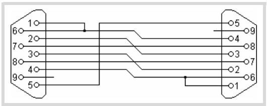
![6○1○\n7○2○\n8○3○\n9○4○\n5○\n5○\n9○9\n4○8\n3○7\n2○6\n1○](.cpci-6910-manual-13/59042f08ff3ce84a25163ab7e236b661c6ce71adb00f67aa89fcb1f6e034078f.jpg)

Figure 10-1: Null Modem Connection

# Setting up the Server Computer

The server computer used in the following guide is a CPU board with an Award Preboot Agent integrated in the BIOS. To support serial console, the BIOS parameters must be adjusted accordingly. When you turn on the computer, enter the BIOS setup, then go to the Advanced BIOS Features menu. Refer to section 8.3 for details.

# Using Serial Console with HyperTerminal

HyperTerminal is a console utility included in Windows operating systems such as Windows $^{®}$ 98/NT/2000. Other console utilities may also be used for remote controlling. If HyperTerminal is not installed in your system, use the Add/Remove Program Properties in the Control Panel to install. Check the HyperTerminal item, then click on OK to install.
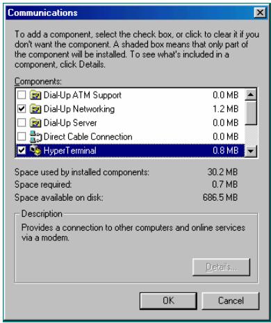
![Communications\nTo add a component, select the check box, or click to clear it if you don't want the component. A shaded box means that only part of the component will be installed. To see what's included in a component, click Details.\nComponents:\nDial-Up ATM Support 0.0 MB\nDial-Up Networking 1.2 MB\nDial-Up Server 0.0 MB\nDirect Cable Connection 0.0 MB\nHyperTerminal 0.8 MB\nSpace used by installed components: 30.2 MB\nSpace required: 0.7 MB\nSpace available on disk: 686.5 MB\nDescription\nProvides a connection to other computers and online services via a modem.\nDetails...\nOK Cancel](.cpci-6910-manual-13/20aeafd1840aca6e82303187704ac190fcdae0196d2853e6ebbf06976e52c3ea.jpg)

# To use HyperTerminal:

# NOTE

The following illustrations use HyperTerminal under Windows $^{®}$ 98 SE operating system.

1. Click Start > Accessories > Communications > HyperTerminal.
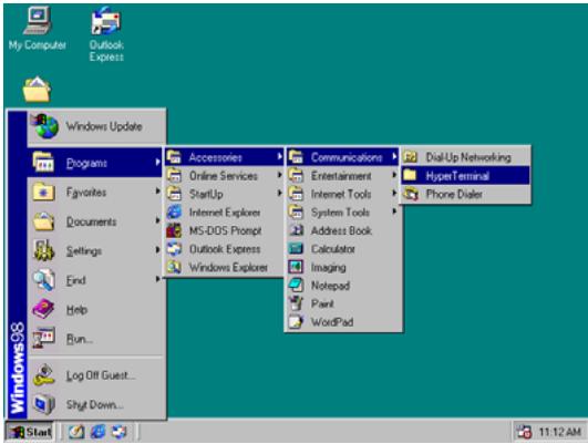
![My Computer\nOutlook Express\nWindows Update\nPrograms\nFavorites\nDocuments\nSettings\nEnd\nHelp\nRun...\nLog Off Guest...\nShift Down...\nStart\nAccessories\nOnline Services\nStartUp\nInternet Explorer\nMS-DOS Prompt\nOutlook Express\nWindows Explorer\nCommunications\nEntertainment\nInternet Tools\nSystem Tools\nAddress Book\nCalculator\nImaging\nNotepad\nPaint\nWordPad\nDial-Up Networking\nHyperTerminal\nPhone Dialer\n11:12 AM](.cpci-6910-manual-13/a2f5ae919f8d6a11ed25b9988fc594f247859dd78fa0d8960f9878b4aa027ef0.jpg)

2. Double-click on the HyperTerminal icon.
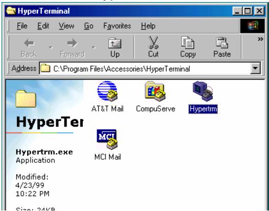
![HyperTerminal\nFile Edit View Go Favorites Help\nBack Forward Up Cut Copy Paste\nAddress C:\Program Files\Accessories\HyperTerminal\nHyperTer\nAT&T Mail CompuServe Hypertrm\nHypertrm.exe\nApplication MCI Mail\nModified:\n4/23/99\n10:22 PM\nSize: 24KB](.cpci-6910-manual-13/1d162d485136d66295bcd54b38b53f7d0cb20ebc5b29742eefaf11f26b5010f4.jpg)

3. When prompted to install a modem before running HyperTerminal, click No.
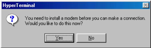
![HyperTerminal\nYou need to install a modem before you can make a connection.\nWould you like to do this now?\nYes	No](.cpci-6910-manual-13/dd44dbe2f4fc9ca18def4fd5e6c6611f072349669a27a87d9b2c69845cdc9b7c.jpg)

4. When the Connection Description window appears, key-in a name for the serial connection, click on 📄, then click OK.
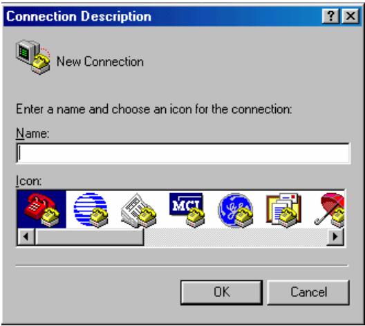
![Connection Description\nNew Connection\nEnter a name and choose an icon for the connection:\nName:\nIcon:\nOK	Cancel](.cpci-6910-manual-13/bdff38a516701360f112abf86999b42f11ca8e08331ca228af9887df74981ac7.jpg)

5. After building the connection node, select the serial port that will connect to the server computer from the Connect using: field, then click OK.
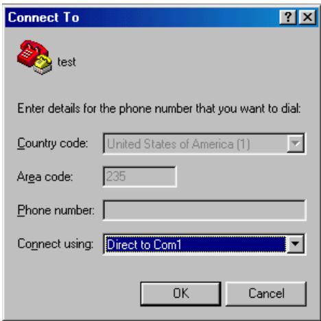
![Connect To\ntest\nEnter details for the phone number that you want to dial:\nCountry code: United States of America (1)\nArea code: 235\nPhone number:\nConnect using: Direct to Com1\nOK Cancel](.cpci-6910-manual-13/33b4118164b36db30f8934cc0365294046657d4d8831d76faac3dcf805269172.jpg)

6. When the serial port's properties window appears, set the Bits per second (Baud rate) the same as with the server computer's Baud rate, click on Apply, then click OK.
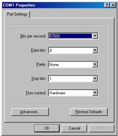
![COM1 Properties\nPort Settings\nBits per second: 57600\nData bits: 8\nParity: None\nStop bits: 1\nFlow control: Hardware\nAdvanced...\nRestore Defaults\nOK    Cancel    Apply](.cpci-6910-manual-13/b2956ab50de0c6f9b95ed84d52f903ed2791991c447e8d2e9ce3a9dbda96fcca.jpg)

7. The HyperTerminal main window appears. Click File > Properties to adjust the connection properties.
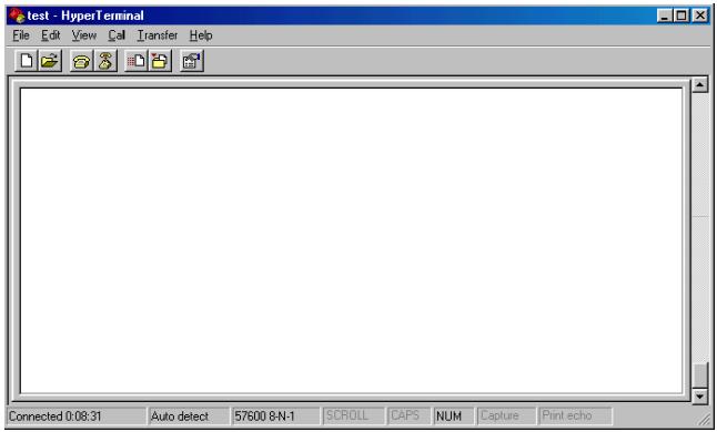
![test - HyperTerminal\nFile Edit View Call Transfer Help\nConnected 0:08:31 Auto detect 57600 8-N-1 SCROLL CAPS NUM Capture Print echo](.cpci-6910-manual-13/bb05c0dd1b2b9e01501ea54f7d3397493ad921dd7672d010f145715cb63b699d.jpg)

8. From the connection Properties window, click the Settings tab, then check if the Telnet terminal mode is set to ANSI. When finished, click the ASCII Setup button.
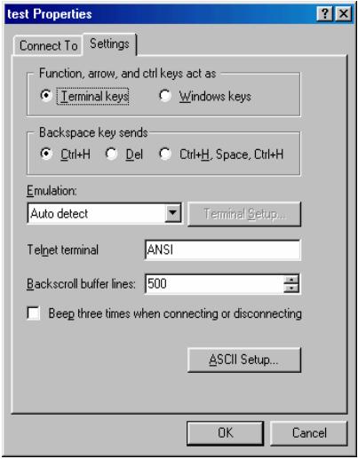
![Test Properties\nConnect To Settings\nFunction, arrow, and ctrl keys act as:\nTerminal keys Windows keys\nBackspace key sends\nCtrl+H Del Ctrl+H, Space, Ctrl+H\nEmulation:\nAuto detect Terminal Setup...\nTelnet terminal ANSI\nBackscroll buffer lines: 500\nBeep three times when connecting or disconnecting\nASCII Setup...\nOK Cancel](.cpci-6910-manual-13/506a1275628b75bfe9b30ff9dfa721e40058a1330feb24b6182e3543bc5f37ce.jpg)

9. To echo the data that the client computer sends, check all options in the ASCII Setup window, then click OK.
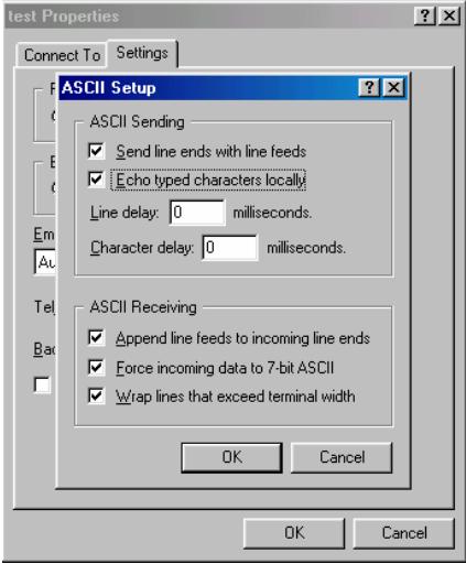
![Test Properties\nConnect To	Settings\nASCII Setup\nASCII Sending\nSend line ends with line feeds\nEcho typed characters locally\nLine delay: 0 milliseconds.\nCharacter delay: 0 milliseconds.\nASCII Receiving\nAppend line feeds to incoming line ends\nForce incoming data to 7-bit ASCII\nWrap lines that exceed terminal width\nOK	Cancel\nOK	Cancel](.cpci-6910-manual-13/965081af1725c4c20239df700d156423f769daab2a85d2f1d8140aee2ab8cd0b.jpg)

10. When HyperTerminal is properly set up and the serial cable is properly connected, power on the server computer. The POST messages of the server computer is displayed in the HyperTerminal console.
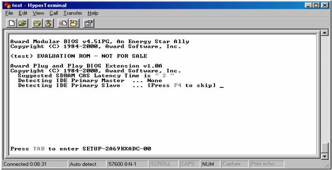
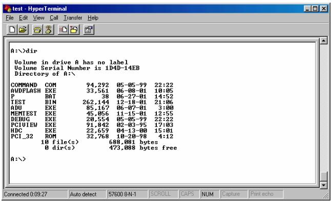
![Award Modular BIOS v4.51PG, An Energy Star Ally\nCopyright (C) 1984-2000, Award Software, Inc.\n(test) EVALUATION ROM - NOT FOR SALE\nAward Plug and Play BIOS Extension v1.00\nCopyright (C) 1984-2000, Award Software, Inc.\nSuggested SDRAM CAS Latency Time is '2'\nDetecting IDE Primary Master ... None\nDetecting IDE Primary Slave ... (Press P4 to skip) _\nPress TAB to enter SETUP-2A69KXADC-00\nConnected 0:08:31 Auto detect 57600 8N-1 SCROLL CAPS NUM Capture Print echo](.cpci-6910-manual-13/711d0b0636ddecf0acbfa415ace8ddcde53b4c353a340f2908144157fc1754ca.jpg)

![A:\)dir\nVolume in drive A has no label\nVolume Serial Number is 1D4D-14EB\nDirectory of A:\\nCOMMAND COM 94.292 05-05-99 22:22\nAVDFLASH EXE 33.561 06-08-01 10:05\nP BRT 38 06-27-01 14:52\nTEST BIN 262.144 12-18-01 21:06\nADU EXE 85.167 06-07-01 3:00\nMEMTEST EXE 45.056 11-15-01 12:55\nDEBUG EXE 20.554 05-05-99 22:22\nPCIUIEW EXE 91.842 02-03-95 17:03\nHDC EXE 22.659 04-13-00 15:01\nPCI_32 ROM 32.768 10-20-98 4:12\n10 file(s) 688.081 bytes\n0 dir(s) 473.088 bytes free\nA:\)](.cpci-6910-manual-13/7a43f672cff781308a4075ad1a4461a3e6964e061f89aff455b06ce3e758a68f.jpg)

11. After the server computer enters the OS, execute commands through the HyperTerminal console.

# 10.3 Performing Operations in the HyperTerminal Console

The &lt;DEL&gt;, &lt;ESC&gt;, &lt;Page Up&gt;, &lt;Page Down&gt;, &lt;Up Arrow&gt;, &lt;Down Arrow&gt;, &lt;Left Arrow&gt;, and &lt;Right Arrow&gt; keys may not be recognized by the server computer's BIOS through the HyperTerminal console. Use the following key sequences to perform these operations.

<table><tr><td>Function Key/Operation</td><td>Key Sequence</td></tr><tr><td>HOME</td><td>ESC [ 1 ~</td></tr><tr><td>INS</td><td>ESC [ 2 ~</td></tr><tr><td>DEL</td><td>ESC [ 3 ~</td></tr><tr><td>END</td><td>ESC [ 4 ~</td></tr><tr><td>ESC</td><td>ESC ESC</td></tr><tr><td>PG UP</td><td>ESC [ 5 ~</td></tr><tr><td>PG DOWN</td><td>ESC [ 6 ~</td></tr><tr><td>UP ARROW</td><td>ESC [ A</td></tr><tr><td>DOWN ARROW</td><td>ESC [ B</td></tr><tr><td>RIGHT ARROW</td><td>ESC [ C</td></tr><tr><td>LEFT ARROW</td><td>ESC [ D</td></tr><tr><td>Reboot system</td><td>ESC C</td></tr></table>

# Important Safety Instructions

For user safety, please read and follow all instructions, WARNINGS, CAUTIONS, and NOTES marked in this manual and on the associated equipment before handling/operating the equipment.

▶ Read these safety instructions carefully.
- Keep this user’s manual for future reference.
▶ Read the specifications section of this manual for detailed information on the operating environment of this equipment.
▶ When installing/mounting or uninstalling/removing equipment:
▷ Turn off power and unplug any power cords/cables.
▶ To avoid electrical shock and/or damage to equipment:
▷ Keep equipment away from water or liquid sources;
▷ Keep equipment away from high heat or high humidity;
▷ Keep equipment properly ventilated (do not block or cover ventilation openings);
▶ Make sure to use recommended voltage and power source settings;
▶ Always install and operate equipment near an easily accessible electrical socket-outlet;
▷ Secure the power cord (do not place any object on/over the power cord);
▶ Only install/attach and operate equipment on stable surfaces and/or recommended mountings; and,
▷ If the equipment will not be used for long periods of time, turn off and unplug the equipment from its power source.
▶ Never attempt to fix the equipment. Equipment should only be serviced by qualified personnel.

A Lithium-type battery may be provided for uninterrupted, backup or emergency power.

![A yellow triangular warning sign featuring a large black exclamation point in the center. Below the triangle is the text 'CAUTION:'.](.cpci-6910-manual-13/b374c81118f61be73e8c6e43f04037918fb357d2a345c5432d182730dd38c384.jpg)

Information to prevent minor physical injury, component damage, data loss, and/or program corruption when trying to complete a task.

▶ Equipment must be serviced by authorized technicians when:

▷ The power cord or plug is damaged;
▷ Liquid has penetrated the equipment;
▷ It has been exposed to high humidity/moisture;
$\triangleright$ It is not functioning or does not function according to the user's manual;
▷ It has been dropped and/or damaged; and/or,
▷ It has an obvious sign of breakage.

# Warranty Policy

Thank you for choosing ADLINK. To understand your rights and enjoy all the after-sales services we offer, please read the following carefully.

1. Before using ADLINK's products please read the user manual and follow the instructions exactly. When sending in damaged products for repair, please attach an RMA application form which can be downloaded from: http://rma.adlinktech.com/policy/

2. All ADLINK products come with a limited two-year warranty, one year for products bought in China:

The warranty period starts on the day the product is shipped from ADLINK's factory.

▶ Peripherals and third-party products not manufactured by ADLINK will be covered by the original manufacturers' warranty.

For products containing storage devices (hard drives, flash cards, etc.), please back up your data before sending them for repair. ADLINK is not responsible for any loss of data.

▶ Please ensure the use of properly licensed software with our systems. ADLINK does not condone the use of pirated software and will not service systems using such software. ADLINK will not be held legally responsible for products shipped with unlicensed software installed by the user.

For general repairs, please do not include peripheral accessories. If peripherals need to be included, be certain to specify which items you sent on the RMA Request & Confirmation Form. ADLINK is not responsible for items not listed on the RMA Request & Confirmation Form.

3. Repair service is not covered by ADLINK's two-year guarantee in the following situations:

▶ Damage caused by not following instructions in the User's Manual.

▶ Damage caused by carelessness on the user's part during product transportation.

▶ Damage caused by fire, earthquakes, floods, lightening, pollution, other acts of God, and/or incorrect usage of voltage transformers.

▶ Damage caused by inappropriate storage environments such as high temperatures, high humidity, or volatile chemicals.

▶ Damage caused by leakage of battery fluid during or after change of batteries by customer/user.

▶ Damage from improper repair by unauthorized technicians.

▶ Products with altered and/or damaged serial numbers are not entitled to our service.

▶ This warranty is not transferable or extendable.

▶ Other categories not protected under our warranty.

4. Customers are responsible for all fees necessary to transport damaged products to ADLINK.

5. To ensure the speed and quality of product repair, please download an RMA application form from our company website: http://rma.adlinktech.com/policy/Products with attached RMA forms receive priority.

For further questions, please e-mail our FAE staff: service@adlinktech.com.
[🔗 Link to the original document](.cpci-6910-manual-13/cpci-6910-manual-13.pdf)
