# cPCI/PCI-8554/R®
# Multi-functions
# Counter / Timer Card
# User’s Guide
©Copyright 1998\~2002 ADLINK Technology Inc,
All Rights Reserved.
Manual Rev. 1.02: July 31, 2002
Part No: 50-11130-100
The information in this document is subject to change without prior notice in order to improve reliability, design and function and does not represent a commitment on the part of the manufacturer.
In no event will the manufacturer be liable for direct, indirect, special, incidental, or consequential damages arising out of the use or inability to use the product or documentation, even if advised of the possibility of such damages.
This document contains proprietary information protected by copyright. All rights are reserved. No part of this manual may be reproduced by any mechanical, electronic, or other means in any form without prior written permission of the manufacturer.
# Trademarks
NuDAQ, DAQBench are registered trademarks of ADLINK Inc.,
Other product names mentioned herein are used for identification purposes only and may be trademarks and/or registered trademarks of their respective companies.
# Getting service from ADLINK
Customer Satisfaction is the most important priority for ADLINK Tech Inc. If you need any help or service, please contact us.
| ADLINK Technology Inc. |
| Web Site | http://www.adlinktech.com |
| Sales & Service | Service@adlinktech.com |
| Technical Support | NuDAQ + USBDAQ | nudaq@adlinktech.com |
| Automation | automation@adlinktech.com |
| NuIPC | nuipc@adlinktech.com |
| NuPRO / EBC | nupro@adlinktech.com |
| TEL | +886-2-82265877 | FAX | +886-2-82265717 |
| Address | 9F, No. 166, Jian Yi Road, Chungho City, Taipei, 235 Taiwan. |
Please email or FAX us of your detailed information for a prompt, satisfactory and constant service.
| Detailed Company Information |
| Company/Organization | |
| Contact Person | |
| E-mail Address | |
| Address | |
| Country | |
| TEL | | FAX | |
| Web Site | |
| Questions |
| Product Model | |
| Environment to Use | OS:Computer Brand:M/B: CPU:Chipset: BIOS:Video Card:Network Interface Card:Other: |
| Detail Description | |
| Suggestions to ADLINK | |
# Table of Contents
# Tables............ iii
# Figures ....... . iv
# How to Use This Guide....... ... v
# Chapter 1 Introduction ......
1.1 Features . 2
1.2 Applications . 3
1.3 Specifications .. 3
1.4 Software Supporting .. 5
1.4.1 Programming Library . 5
1.4.2 PCIS-LVIEW: LabVIEW® Driver .... 6
1.4.3 PCIS-VEE: HP-VEE Driver .. 6
1.4.4 DAQBenchTM: ActiveX Controls.. 6
# Chapter 2 Getting Started ...... . 7
2.1 What You Have ..
2.2 Unpacking.. /
2.3 PCB Layout of cPCI/PCI-8554/R. .8
2.4 Default Jumper Setting . .9
2.5 cPCI/PCI-8554/R Installation. .11
2.5.1 Hardware configuration.. .11
2.6 Device Installation for Windows Systems .. .12
2.7 Pin Assignment of Connector . .13
2.8 Clock System.. .15
2.9 Counters Architecture. . 15
2.9.1 Independent Counters (Counter 1\~10) . ..17
2.9.2 Cascaded Counters .. .17
2.9.3 User Configurable Cascaded Counters .. ..18
2.10 Clock Source Configurations.. .19
2.11 Gate Control Configurations.. ..20
2.12 Counter Outputs.. . 20
2.13 Debounce System.. .21
2.14 Interrupt System.. . 22
2.15 Digital Input and Output . . 23
2.16 12V and 5V Power Supply . .. 24
# Chapter 3 Registers ......... .. 25
3.1 PCI PnP Registers... .25
3.2 I/O Address Map.. .. 26
3.3 Timer/Counter Registers . .27
3.4 Timer / Counter Clock Mode Control .. ..27
3.5 Digital Input Register . . 28
3.6 Digital Output Register . .29
# Chapter 4 Signal Connections & Applications.................... 30
4.1 Connectors Pin Assignment . .. 30
4.2 Digital I/O Connection.. ..30
4.3 Timer/Counter Connection.. .31
4.4 Frequency Generator . ..32
4.4.1 To generate a 250 KHz Square Wave. .. . 32
4.4.2 To generate a 1 pulse/1 hour signal . . 33
4.5 Pulse Width Measurement.. .34
4.6 Frequency Measurement.. .. 35
4.7 Event Counter... .37
4.8 Dual Interrupt System.. ..38
# Chapter 5 C/C++ Library .......... .. 39
5.1 Libraries Installation.. ..39
5.2 Programming Guide . .. 40
5.2.1 Naming Convention .. ..40
5.2.2 Data Types .. ..40
5.3 \_8554\_Initial .. ..41
5.4 \_8554\_Write\_Counter . .. 42
5.5 \_8554\_Read\_Counter .. .. 43
5.6 \_8554\_Stop\_Counter . .. 44
5.7 \_8554\_Read\_Status.. .. 45
5.8 \_8554\_DO ... .. 46
5.9 \_8554\_DI.. ..47
5.10 \_8554\_SET\_cntCLK . .. 48
5.11 \_8554\_SET\_CK1.. ..49
5.12 \_8554\_SET\_DBCLK . ..50
5.13 \_8554\_Set\_INT\_Control .. .. 51
5.14 \_8554\_Get\_IRQ\_Status. . 52
5.15 \_8554\_INT\_Enable . .53
5.16 \_8554\_INT\_Disable .. . 54
5.17 \_8554\_CLR\_IRQ1 . ..54
5.18 \_8554\_CLR\_IRQ2 . .. 55
# Warranty Policy .......... .... 56
# Tables
Table 1. Default Jumper Settings on PCI-8554 . .. 10
Table 2. Extra Default Jumper Setting on cPCI-8554/R... 10
Table 3. Counters label relationship . . 15
Table 4. I/O Address Map of cPCI/PCI-8554/R . . 26
Table 5. Timer/Counter Registers... . 27
Table 6. Timer/Counter Clock Mode Control Register ... . 28
Table 7. Digital Input Register .. . 28
Table 8. Digital Output Register... . 29
Table 9. Data types and their ranges. . 40
# Figures
Figure 1: Functional Block diagram.. 2
Figure 2: PCB Layout of PCI-8554.. 8
Figure 3: PCB Layout of cPCI-8554/R .. 9
Figure 4: Pin Assignment of PCI-8554 Connector CN1 . . 13
Figure 5: Pin Assignment of cPCI-8554/R Connector CN1.. . 14
Figure 6: Block Diagram of 8254 Counter.. . 16
Figure 7: Default Counters Architectural. . 16
Figure 8: Example of ‘independent counters’. . 17
Figure 9: JP14/JP15 (For cPCI-8554/R only).. . 17
Figure 10: Cascaded Counter Configuration.. . 18
Figure 11: User Programmable Cascaded Counters .. . 18
Figure 12: Clock Source of Counter n.. . 19
Figure 13: Clock Source of CK1 . 19
Figure 14: Gate source of counter 1 \~ 10 .. . 20
Figure 15: Structure of JP1 \~ JP11.. . 21
Figure 16: Clock Source of DB\_CLK . . 21
Figure 17: Basic Timing of the debounce system . . 22
Figure 18: Dual Interrupt System of cPCI/PCI-8554/R. . 22
Figure 19: Digital I/O Connection.. .. 30
Figure 20: Example of a frequency generator (1).. . 32
Figure 21: Example of frequency generator (2)... . 33
Figure 22: Example of pulse width measurement . . 34
Figure 23: Example of frequency measurement (1).. .. 36
Figure 24: Example of event counter .. . 37
Figure 25: Example of dual interrupt system.. . 38
# How to Use This Guide
This manual is designed to help you use the cPCI/PCI-8554/R. The manual describes how to modify various settings on the cPCI/PCI-8554/R card to meet your requirements. It is divided into 5 chapters:
Chapter 1, “Introduction,” gives an overview of the product features, applications, and specifications.
Chapter 2, “Installation & Configurations” describes the operation method and multi-functions of the cPCI/PCI-8554/R. Users should read through this chapter to understand the configurations of the cPCI/PCI-8554/R. The chapter will also outline how to install the cPCI/PCI-8554/R.
Chapter 3, “Registers,” describes the details of each register of the cPCI/PCI-8554/R; this information will assist programmers who want to control the hardware with low-level programming.
Chapter 4, “Signal Connection & Applications,” describes the connectors' pin assignment and how to connect the outside signal and devices to / from the cPCI/PCI-8554/R. Some applications also are introduced.
Chapter 5, “High-level Programming,” introduces the Clanguage library for operating the cPCI/PCI-8554/R. Some examples are shown too.
#
# Introduction
cPCI/PCI-8554/R is a general-purpose counter / timer and digital I/O card. The card is designed with four 8254, a programmable interval timer/counter chip, totally, providing twelve 16-bit down counter or frequency dividers. Three different types of interface are available: PCI (PCI-8554), CompactPCI (cPCI-8554), and CompactPCI with rear I/O connection (cPCI-8554R) for various platforms and applications.
The card has multi-configurations. Its counters can be set in an independent or cascaded configuration. The gate controls for the counter can come from either the internal default enable signal or from external sources. The clock source of the counters can be set from an internal or external clock source, when an external clock source is used, users can configure the jumper as to disable or enable the debounce function.
The card also provides digital input and output ports. There are 8 digital output and 8 digital input channels, which can be used to control or monitor external devices.
The cPCI/PCI-8554/R provides an interrupt signal, which is generated by the counter output. External interrupt signals can also be used. The interrupt can be used for watchdog timers or others applications. The maximum interrupt time interval can be 536 seconds.
The I/O signals are provided via the 100-pin SCSI-II connector. Figure 1 shows the functional block diagram of the cPCI/PCI-8554/R. The cPCI/PCI-8554/R uses ASIC PCI controller to interface the board to the PCI bus. The ASIC fully implements the PCI local bus specification Rev 2.1. The BIOS software automatically controls all bus relative configurations, such as base memory and interrupt assignment. This removes the burden of searching for a conflict, which can be very time consuming and difficult with some bus standards.
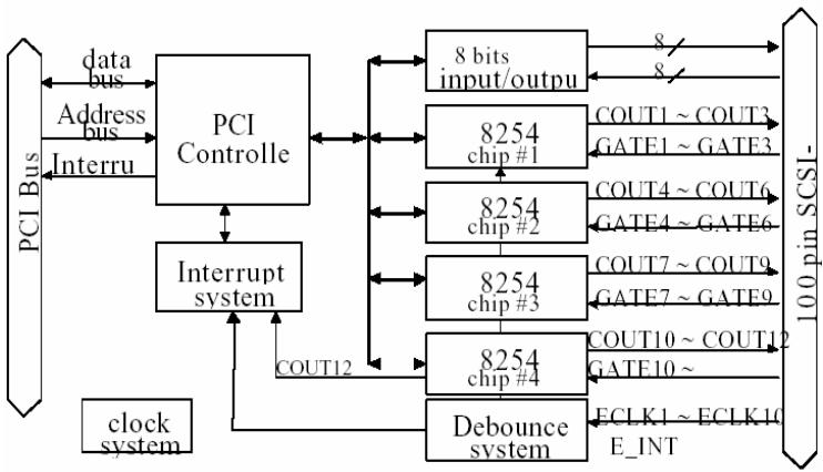
Figure 1: Functional Block diagram
# 1.1 Features
The cPCI/PCI-8554/R Counter / Timer and digital I/O Card provides the following advanced features:
• Four 8254 chips provide twelve 16 bits down counters
Multi-configurations of counters / timers:
Flexible setting for each independent counter, the clock source could be external, internal or cascaded. The gate signal is external controlled or internal enabled.
Provide debounce function with flexible setting to prevent from bounce phenomenon when using external clocks.
• 8 digital output channels
• 8 digital input channels
Dual interrupt sources
3 From output of counter #12, or
3 From external source.
100-pin SCSI-II female connector.
• PCI-Bus
# 1.2 Applications
• Event counter
Frequency generator
Frequency synthesizer
Pulse width measurement
• Low level pulse generator
Time delay
Industry automation
Watchdog timer
# 1.3 Specifications
# Programmable Counter / Timer
Device: 82C54x4
Number of Counters/timers:
3 10 independent timers / counters
3 2 cascaded timers / counters
3 Cascaded 32-bit counters with fixed 8MHz internal clock
• Counter mode: 16-bit down counter
Maximum input frequency: 8 MHz
Clock sources of independent counters:
3 External clock
3 Prior counter output
3 Clock #10 output
3 CK1 (Programmable)
CK1 clock sources: (Programmable)
3 8MHz internal base clock
3 Programmable counter 11 output
Gate control: default enable or external control
# Digital Filter Circuits
Device: MC14490
De-bounce clock: (Programmable)
3 8MHz internal base clock
3 Programmable counter 11 output
# Digital I/O (DIO)
• No. of input channels : 8 channels
No. of output channels : 8 channels (dedicated output)
Characteristics: TTL compatible signal
# General Specifications
Connector: 100-pin SCSI-II female connector
Operating Temperature: 0°C \~ 60°C
Storage Temperature: -20°C \~ 80°C
• Humidity: 5 \~ 95%, non-condensing
• Power Consumption: +5 V @ 350 mA typical
Dimension: 134mm(L) X 107mm(W)
# 1.4 Software Supporting
ADLINK provides versatile software drivers and packages for users’ different approach to building a system. ADLINK not only provides programming libraries such as DLL for most Windows based systems, but also provide drivers for many other software packages such as LabVIEW®, HP VEETM, DASYLabTM, InTouchTM, InControlTM, ISaGRAFTM, and so on.
All software options are included in the ADLINK CD. Non-free software drivers are protected with licensing codes. Without the software code, you can install and run the demo version for two hours for trial/demonstration purposes. Please contact ADLINK dealers to purchase the formal license.
# 1.4.1 Programming Library
For customers who are writing their own programs, we provide function libraries for many different operating systems, including:
DOS Library: Borland C/C++ and Microsoft C++, the functional descriptions are included in this user’s guide.
Windows 95 DLL: For VB, VC++, Delphi, BC5, the functional descriptions are included in this user’s guide.
PCIS-DASK: Include device drivers and DLL for Windows 98, Windows NT and Windows 2000. DLL is binary compatible across Windows 98, Windows NT and Windows 2000. This means all applications developed with PCIS-DASK are compatible with Windows 98, Windows NT and Windows 2000. The developing environment can be VB, VC++, Delphi, BC5, or any Windows programming language that allows calls to a DLL. The user’s guide and function reference manual of PCIS-DASK are included in the CD. Please refer to the PDF files under \\Manual\_PDF\Software\PCIS-DASK
PCIS-DASK/X: Include device drivers and shared library for Linux. The developing environment can be Gnu C/C++ or any programming language that allows linking to a shared library. The user's guide and function reference manual of D2K-DASK/X are included in the CD. (\Manual\_PDF\Software\D2K-DASK-X.)
The above software drivers are shipped with the board. Please refer to the “Software Installation Guide” for installation procedures.
# 1.4.2 PCIS-LVIEW: LabVIEW® Driver
PCIS-LVIEW contains the VIs, which is used to interface with the NI LabVIEW® software package. The PCIS-LVIEW supports Windows 95/98/NT/2000. The LabVIEW® drivers are shipped free with the board. For more information about PCIS-LVIEW, please refer to the user’s guide in the CD. (\\Manual\_PDF\Software\PCIS-LVIEW)
# 1.4.3 PCIS-VEE: HP-VEE Driver
The PCIS-VEE includes user objects, which are used to interface with the HP VEE software package. PCIS-VEE supports Windows 95/98/NT. The HP-VEE drivers are shipped free with the board. For more information about PCIS-VEE, please refer to the user’s guide in the CD. (\\Manual\_PDF\Software\PCIS-VEE)
# 1.4.4 DAQBenchTM: ActiveX Controls
We suggest customers who are familiar with ActiveX controls and VB/VC++ programming use the DAQBenchTM ActiveX Control components library for developing applications. The DAQBenchTM is designed under Windows NT/98. For more information about DAQBench, please refer to the user’s guide in the CD. (\\Manual\_PDF\Software\DAQBench\DAQBench Manual.PDF)
# 2
# Getting Started
This chapter discusses how to setup the cPCI/PCI-8554R and configure the card to meet the requirements of your application. The contents of the package and unpacking information that you should be aware off are outlined first.
# 2.1 What You Have
In addition to this User's Manual, the package should includes the following items:
cPCI/PCI-8554/R Enhanced Multi-function Counter / Timer Card
ADLINK CD
Software Installation Guide
If any of these items are missing or damaged, contact the dealer from whom you purchased the product. Save the shipping materials and carton in case you want to ship or store the product in the future.
# 2.2 Unpacking
Your cPCI/PCI-8554/R card contains electro-static sensitive components that can be easily be damaged by static electricity.
Therefore, the card should be handled on a grounded anti-static mat. The operator should be wearing an anti-static wristband, grounded at the same point as the anti-static mat.
Inspect the card module carton for obvious damages. Shipping and handling may cause damage to your module. Be sure there are no shipping and handling damages on the modules carton before continuing.
After opening the card module carton, extract the system module and place it only on a grounded anti-static surface with component side up.
Again, inspect the module for damages. Press down on all the socketed $| \check { \mathbf { C } ^ { \prime } } \mathsf { s }$ to make sure that they are properly seated. Do this only with the module placed on a firm flat surface.
Note: DO NOT APPLY POWER TO THE CARD IF IT HAS BEEN DAMAGED.
You are now ready to install your cPCI/PCI-8554/R.
# 2.3 PCB Layout of cPCI/PCI-8554/R
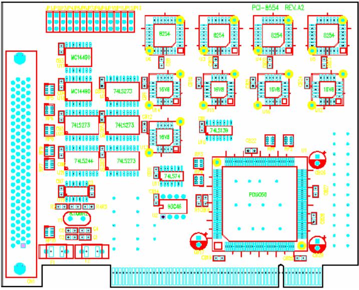
Figure 2: PCB Layout of PCI-8554
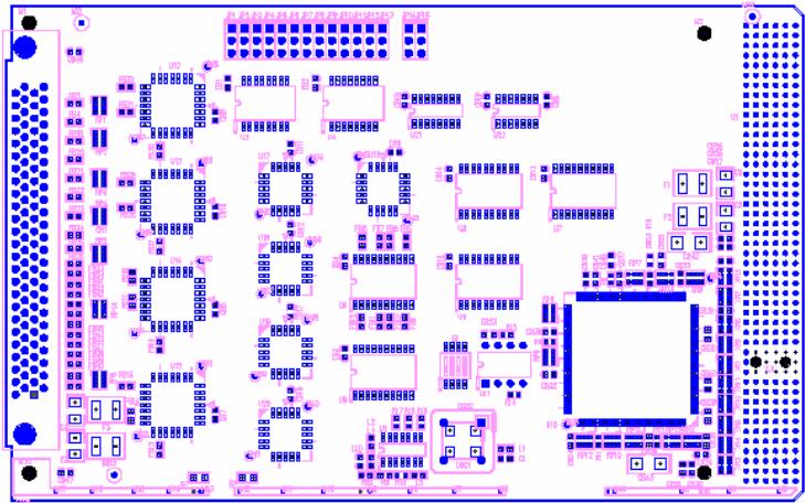
Figure 3: PCB Layout of cPCI-8554/R
# 2.4 Default Jumper Setting
To operate the cPCI/PCI-8554/R correctly, users need to understand the structure of cPCI/PCI-8554/R and details of the possible configurations. The functional block diagram of the cPCI/PCI-8554/R is shown in figure 1 of chapter 1. The following section lists the default jumper setting on the cPCI/PCI-8554/R.
| Items | Default Configuration | Set by |
| ECLK1 | No Debounce function | JP1 |
| ECLK2 | No Debounce function | JP2 |
| ECLK3 | No Debounce function | JP3 |
| ECLK4 | No Debounce function | JP4 |
| ECLK5 | No Debounce function | JP5 |
| ECLK6 | No Debounce function | JP6 |
| ECLK7 | No Debounce function | JP7 |
| ECLK8 | No Debounce function | JP8 |
| ECLK9 | No Debounce function | JP9 |
| ECLK10 | No Debounce function | JP10 |
| E_INT | No Debounce function | JP11 |
| ECLK11 | Internal 8MHz Clock | JP12 |
| ECLK12 | Output of CLK11 | JP13 |
Table 1. Default Jumper Settings on PCI-8554
| Items | Default Configuration | Set by |
| GATE11 | Vcc | JP14 |
| GATE12 | Vcc | JP15 |
Table 2. Extra Default Jumper Setting on cPCI-8554/R
There are 13 jumpers available on the PCI-8554, and 15 jumpers on the cPCI-8554/R, the first 11 jumpers are used to select the debounce function. JP12 and JP13 are used for selecting the clock source for Counter No. 11 and 12. The default setting for counter No. 11 and 12 are cascaded for frequency division. Refer to section 2.9 for more details. JP14 and JP15 are used for selecting the gate voltages of counter No. 11 and 12 (only for cPCI-8554/R). Users can change the cPCI/PCI-8554/R's default configuration by setting jumpers on the card to suit the application. The card's jumpers are preset at the factory.
Before changing the default configuration, users must fully understand the operation of the debounce function. The setting and the basic operation theory are not discussed in this chapter. Refer to section 2.12 for details of the operation theory and than refer to chapter 4 for application notes.
# 2.5 cPCI/PCI-8554/R Installation
# 2.5.1 Hardware configuration
The PCI cards (or CompactPCI cards) is equipped with the plug and play PCI controller, it has the ability to request base addresses and interrupts according to the PCI standard. The systems BIOS will install the system resources based on the PCI cards’ configuration registers and system parameters (which are set by system BIOS). Interrupt assignments and memory usage (I/O port locations) of the PCI cards are also assigned by system BIOS. This system resource assignment is done on a board-byboard basis. It is not suggested to assign system resources by any other methods.
The PCI card can be inserted into any PCI slot without the need for any system resource configuration.
# 2.5.1.1 Installation Procedures
1. Turn off your computer
2. Turn off all accessories (printer, modem, monitor, etc.) connected to your computer.
3. Remove the cover from your computer.
4. Setup jumpers on the PCI or CompactPCI card.
5. Select a 32-bit PCI slot. PCI slot are shorter than ISA or EISA slots, and are usually white or ivory in color.
6. Before handling the PCI cards, discharge any static buildup on your body by touching the metal case of the computer. Hold the edge and do not touch the components.
7. Position the board into the PCI slot you selected.
8. Secure the card in place at the rear panel of the system.
# 2.6 Device Installation for Windows Systems
Once Windows 95/98/2000 has started, the Plug and Play function of the Windows OS will find the new NuDAQ/NuIPC cards. If this is the first time a NuDAQ/NuIPC cards is installed into the computer system. The Windows operating system will inform you to input the device information source. Please refer to the “Software Installation Guide” for installation procedures.
# 2.7 Pin Assignment of Connector
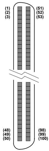
| (1) +12V | (26) GND | (51) GND | (76) ECLK9 |
| (2) +12V | (27) GND | (52) GOUT2 | (77) COUT8 |
| (3) +12V | (28) GND | (53) GIN2 | (78) GATE8 |
| (4) Vcc | (29) GND | (54) GND | (79) ECLK8 |
| (5) Vcc | (30) GND | (55) GOUT1 | (80) COUT7 |
| (6) Vcc | (31) GND | (56) GIN1 | (81) GATE7 |
| (7) NC | (32) GND | (57) E_INT | (82) ECLK7 |
| (8) DI_6 | (33) GND | (58) DI7 | (83) COUT6 |
| (9) DI_4 | (34) GND | (59) DI5 | (84) GATE6 |
| (10) DI_2 | (35) GND | (60) DI3 | (85) ECLK6 |
| (11) DI_0 | (36) GND | (61) DI1 | (86) COUT5 |
| (12) DO_6 | (37) GND | (62) DO7 | (87) GATE5 |
| (13) DO_4 | (38) GND | (63) DO5 | (88) ECLK5 |
| (14) DO_2 | (39) GND | (64) DO3 | (89) COUT4 |
| (15) DO_0 | (40) GND | (65) DO1 | (90) GATE4 |
| (16) NC | (41) GND | (66) ECLK12 | (91) ECLK4 |
| (17) GND | (42) GND | (67) COUT12 | (92) COUT3 |
| (18) GND | (43) GND | (68) ECLK11 | (93) GATE3 |
| (19) GND | (44) GND | (69) COUT11 | (94) ECLK3 |
| (20) GND | (45) GND | (70) GND | (95) COUT2 |
| (21) GND | (46) GND | (71) COUT10 | (96) GATE2 |
| (22) GND | (47) GND | (72) GATE10 | (97) ECLK2 |
| (23) GND | (48) GND | (73) ECLK10 | (98) COUT1 |
| (24) GND | (49) GND | (74) COUT9 | (99) GATE1 |
| (25) GND | (50) GND | (75) GATE9 | (100) ECLK1 |
Figure 4: Pin Assignment of PCI-8554 Connector CN1
Legend:
| ECLK n: | External clock source for counter #n |
| ExtG n: | External gate signal for counter #n |
| COUT n: | Counter / Timer output of counter #n |
| DO_m: | Digital output port channel #m |
| DI_m: | Digital input port channel #m |
| E_int: | External interrupt signal input |
| GOUT1: | Inverse TTL signal of GIN1 |
| GOUT2: | Inverse TTL signal of GIN2 |
| NC: | No Connection |
(1) +12V
(26) GND
(51) GND
(76) ECLK9
| (2) +12V | (27) GND | (52) GOUT2 | (77) COUT8 |
| (3) +12V | (28) GND | (53) GIN2 | (78) GATE8 |
| (4) Vcc | (29) GND | (54) GND | (79) ECLK8 |
| (5) Vcc | (30) GND | (55) GOUT1 | (80) COUT7 |
| (6) Vcc | (31) GND | (56) GIN1 | (81) GATE7 |
| (7) GATE12 | (32) GND | (57) E_INT | (82) ECLK7 |
| (8) DI_6 | (33) GND | (58) DI7 | (83) COUT6 |
| (9) DI_4 | (34) GND | (59) DI5 | (84) GATE6 |
| (10) DI_2 | (35) GND | (60) DI3 | (85) ECLK6 |
| (11) DI_0 | (36) GND | (61) DI1 | (86) COUT5 |
| (12) DO_6 | (37) GND | (62) DO7 | (87) GATE5 |
| (13) DO_4 | (38) GND | (63) DO5 | (88) ECLK5 |
| (14) DO_2 | (39) GND | (64) DO3 | (89) COUT4 |
| (15) DO_0 | (40) GND | (65) DO1 | (90) GATE4 |
| (16) GATE11 | (41) GND | (66) ECLK12 | (91) ECLK4 |
| (17) GND | (42) GND | (67) COUT12 | (92) COUT3 |
| (18) GND | (43) GND | (68) ECLK11 | (93) GATE3 |
| (19) GND | (44) GND | (69) COUT11 | (94) ECLK3 |
| (20) GND | (45) GND | (70) GND | (95) COUT2 |
| (21) GND | (46) GND | (71) COUT10 | (96) GATE2 |
| (22) GND | (47) GND | (72) GATE10 | (97) ECLK2 |
| (23) GND | (48) GND | (73) ECLK10 | (98) COUT1 |
| (24) GND | (49)GND | (74) COUT9 | (99) GATE1 |
| (25) GND | (50) GND | (75) GATE9 | (100) ECLK1 |
Figure 5: Pin Assignment of cPCI-8554/R Connector CN1
# Legend:
ECLK n: External clock source for counter #n
ExtG n: External gate signal for counter #n
COUT n: Counter / Timer output of counter #n
DO\_m: Digital output port channel #m
DI\_ m: Digital input port channel #m
$E _ { - } i n t { : }$ External interrupt signal input
GOUT1: Inverse TTL signal of GIN1
GOUT2: Inverse TTL signal of GIN2
Note: pin-7and pin-16 is different from the definition in PCI-8554.
# 2.8 Clock System
The clock system of the cPCI/PCI-8554/R provides the internal clock source for the 8254 chips. The clock for counter/timer 1 \~ 10 can be one of 4 sources; an external clock source, a cascaded source from the ‘last’ channel, CK1 or COUT10. The next section will outline details on setting the clock for each counter/timer and CK1. The clock of counter/timer 11 is fixed at 8Mhz, and the clock of counter/timer 12 is connected to COUT11
# 2.9 Counters Architecture
There are four 8254 programmable timer/counter chips on the cPCI/PCI-8554/R card. Each 8254 chip contains 3 counter/timer and are labeled from 1 to 12. Counters 11 and 12 are default cascaded counters, but can be set for independent operation through jumpers JP12 & JP13. Counters 1 \~ 10 can also be set as an independent or cascaded counters. Table 3 illustrates the relationship between the reference 8254-chip label and the counter labels.
| 8254 Chip Label | Reference Number | Counter Label | Type of Counter |
| Chip 1 | U3 | Counter 1 | Independent or Cascaded |
| Counter 2 | Independent or Cascaded |
| Counter 3 | Independent or Cascaded |
| Chip 2 | U4 | Counter 4 | Independent or Cascaded |
| Counter 5 | Independent or Cascaded |
| Counter 6 | Independent or Cascaded |
| Chip 3 | U5 | Counter 7 | Independent or Cascaded |
| Counter 8 | Independent or Cascaded |
| Counter 9 | Independent or Cascaded |
| Chip 4 | U6 | Counter 10 | Independent or Cascaded |
| Counter 11 | Independent or Cascaded |
| Counter 12 | Independent or Cascaded |
Table 3. Counters label relationship
There are three signals (2 input and 1 output) for each counter, a clock input signal, a gate control signal, and an output signal. Figure 6 illustrates the block diagram of the 8254 counter. CLK1 \~ CLK12 are clock sources, GATE1 \~ GATE12 are gate control signals and COUT1 \~ COUT12 are outputs of the counters. Figure 7 shows the inter-connection of the 8254 counters and the labels associated to each counter.

Figure 6: Block Diagram of 8254 Counter
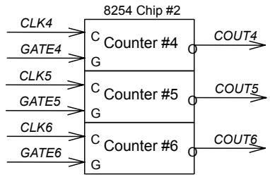
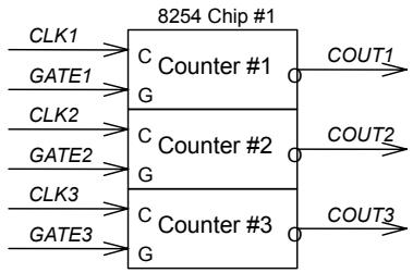
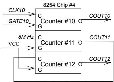
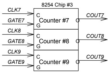
Figure 7: Default Counters Architectural
# 2.9.1 Independent Counters (Counter 1\~10)
Counters 1 to 10 are independent counters because the clock source and gate control of those counters can be set independently (Thus named Independent Counter).
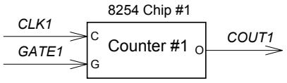
Figure 8: Example of ‘independent counters’
# 2.9.2 Cascaded Counters
The connection of Counter 11 and 12 are different from the independent counters. These two counters are cascaded counters by default settings. The clock source of counter 11 is set to the internal 8 MHz clock by JP12, while JP13 connects its output to counter 12. In fact, counter 11and 12 are designed for frequency division by using the 8254's square wave generator mode. The gates of these counters are by default tied to logic high (‘H’) to enable these counters at all times. Users can change JP14 and JP15 to tie the signal to the GATE pins.
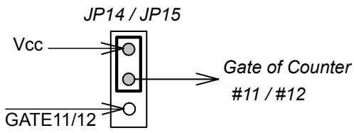
Figure 9: JP14/JP15 (For cPCI-8554/R only)
COUT12 can precisely generate frequencies up to 2MHz and as low as 0.00186 Hz. Note that the COUT12 signal can also be used as an interrupt source. See ‘Interrupt Sources’ section for details. Figure 10 illustrates the cascaded counters - counters 11 and 12. Sometimes, you may require all 12 counters to operate independently. For such a case, you can break the default connection by reconfiguring jumpers J12 and J13. Note that both counters 11 and 12 only have 2 selectable clock sources. It can be either the 8 MHz internal clock source or an external clock source.
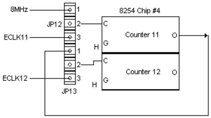
Figure 10: Cascaded Counter Configuration
# 2.9.3 User Configurable Cascaded Counters
Although by default there is only one cascaded counter, users can configure the independent counters to be in a cascaded arrangement by using the \_SET\_cntCLK\_ function. . Figure 11 illustrates the user programmable-cascaded counter. Refer to the next section for details of the clock source options.
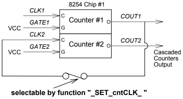
Figure 11: User Programmable Cascaded Counters
# 2.10 Clock Source Configurations
For each independent counter, one of four different clock sources maybe selected using the software. The clock source of counter n can be either an external clock source (ECLK n), a cascaded counter output (COUTn-1), CK1 or COUT10.
# Note:
1. The clock source of cascaded counter 11 is set at C8M (8MHz) and counter 12 is set to COUT11.
2. The external clock source labelled ECK n comes from JP1 \~ JP10, see section 2.12 for details
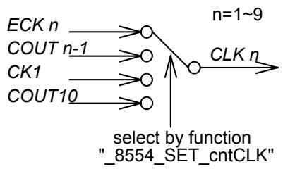
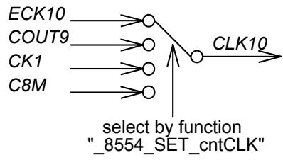
Figure 12: Clock Source of Counter n
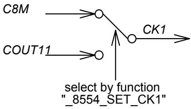
Figure 13: Clock Source of CK1
The internal clock sources of CK1 can be either C8M or COUT11, and is selected by using the “\_8554\_SET\_CK1” function. If the counters are set in a cascaded configuration, then the clock source will be from the output of the previous counter (Counter n-1). For example, COUT1 is cascaded to CLK2; COUT3 is cascaded to CLK4 and so on. (Note: If counter 1 is set in cascaded mode, CLK1 is connected to GND because COUT0 doesn’t exist).
# 2.11 Gate Control Configurations
The gate control signals of each independent counter is internally pulled high hence they are Enabled by default if no external gate is used. When an external gate signal is used, the counters can be used for pulse width measurements. Therefore, the period of the gate signal can be precisely controlled and frequency measurement is possible. Figure 14 shows the settings for the gate signals of counters 1\~ 10. (Note: The gate signals of counter 11 and 12 are always pulled high)
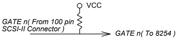
Figure 14: Gate source of counter 1 \~ 10
# 2.12 Counter Outputs
The clock source, gate signal and software programming controls the timer/counter output signal “COUT n”. All outputs from the 12 counters are routed to the 100-pin connector. Refer to the figure 4 and 5 for the corresponding signal pin number.
In addition, the output signal may be used as a clock source for cascaded configuration, see the above sections for details. It is possible to cascade all ten counters using the software settings, see 2.8 for reference. The output COUT12 can also be used as an internal interrupt source (refers to 'Interrupt System' for details).
# 2.13 Debounce System
The debounce system is used to eliminate the affects of bounce phenomenons. If an external clock is used, user can set JP1 \~ JP11 to select, whether or not to used the debounce system. If the debounce system is used, the debounce output signal will be in the same state as the input only if the input signal maintains the same state for four DB\_CLK cycles, otherwise the input signal will be treated as a glitch and the debounce output signal will maintain its present state, figure 15 illustrates how to set these jumpers, figure 16 illustrates how to select the DB\_CLK. Figure 17 illustrates the basic timing of the debounce system. (Note: DB\_CLK can’t be higher than 2MHz).
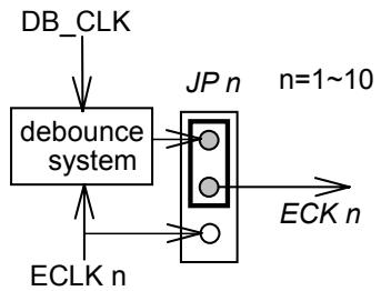
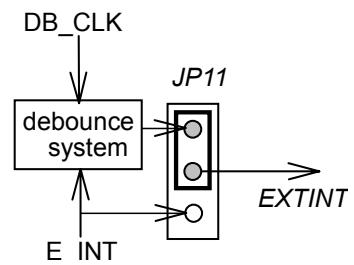
Figure 15: Structure of JP1 \~ JP11
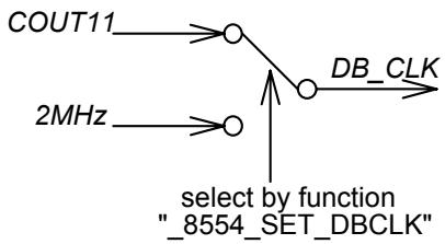
Figure 16: Clock Source of DB\_CLK
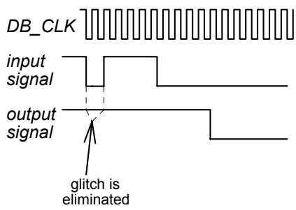
Figure 17: Basic Timing of the debounce system
# 2.14 Interrupt System
The cPCI/PCI-8554/R‘s interrupt system is a powerful and flexible system, which is suitable for many applications. The system is a Dual Interrupt System. Dual Interrupt means the hardware can generate two interrupt request signals simultaneously and the software is able to respond and invoke the ISR. Note that dual interrupt do not mean the card will occupy two IRQ levels. These two interrupt request signals INT1 and INT2 are generated by the external interrupt signal EXTINT and the timer/counter 12 output. Figure 18 shows the structure of interrupt system.
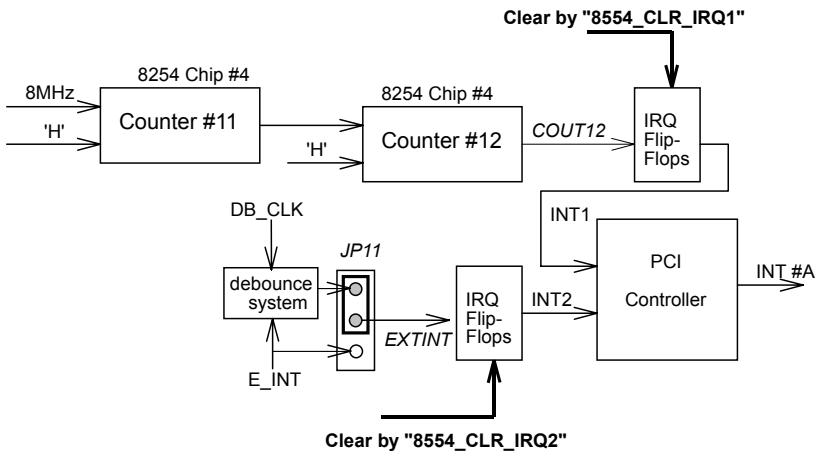
Figure 18: Dual Interrupt System of cPCI/PCI-8554/R
Even though it is a dual interrupt system, only one interrupt level is ever used. The card uses the INT #A interrupt request signal on the PCI bus. The motherboards circuits will then transfer INT #A to one of the AT bus IRQ levels. The IRQ level is set by the PCI plug and play BIOS and is saved in the PCI controller. It is not necessary for users to set the IRQ level. Users can however read back the IRQ level setting by using the software library. Refer to the section 5.4.
The PCI controller of cPCI/PCI-8554/R can receive two hardware IRQ sources. However, a PCI controller can generate only one IRQ to the PCI bus, the two IRQ sources are distinguished by the ISR software. If both IRQ are in use, the application software will invoke the “\_8554\_GET\_IRQ\_Status” function to distinguish which interrupt is inserted and servicing that IRQ. Users must then clear the current IRQ to allow the next IRQ be processed.
If the application needs only one IRQ, the other IRQ source can be disabled by software. If your application does not require any IRQ sources, you can disable both interrupts. However, the PCI BIOS will still assign an IRQ level to the PCI card and hence will still occupy the PC’s resources if you only disable the IRQ sources without changing the initial conditions of the PCI controller. It is however, not recommended that the user re-design the initial condition of the PCI card with the users’ own application software. If users want to disable the IRQ level, user can use the ADLINK utility ‘INIT8554.EXE’ to change the interrupt settings.
# 2.15 Digital Input and Output
To program the digital I/O operation is fairly straightforward. The digital input operation is used for reading data from its corresponding registers, and the digital output operation is used for writing data to its corresponding registers. The digital I/O registers‘ are discussed in section 3.4 and 3.5.
# 2.16 12V and 5V Power Supply
The 100-pin SCSI-II connector provides +12 and +5 volt power sources. To avoid shorts or overloads of the power sources, thermistors are added to all power supply rails. The current rating of the +5 volt supply thermistor is 500 mA. If the load current is larger than 500mA, the resistance of the thermistors will increase due to the temperature rise. The rising resistance drops the supply voltage and hence reduces the current. If the overload or short condition is cleared, the thermistor will return to normal operation. The +12V supply thermistor also has the same current rating characteristics as the +5V supply.
# 3
# Registers
Detailed descriptions of the registers are specified in this chapter. This information is useful for programmers who wish to handle the card with low-level programming. However, we suggest users to an understanding of the PCI interface before starting any low-level programming. In addition, the contents of this chapter will also help users understand how to use the software drivers to configure this card.
# 3.1 PCI PnP Registers
This PCI card functions as a 32-bit PCI target device to any master on the PCI bus. There are three types of registers: PCI Configuration Registers (PCR), Local Configuration Registers (LCR) and cPCI/PCI-8554/R registers.
The PCR, which is PCI-bus specifications compliant, is initialized and controlled by the plug & play (PnP) PCI BIOS. Users may obtain more information on the PCI BIOS specification to better understand the operation of the PCR. Please contact PCISIG to acquire the specifications of the PCI interface.
The PCI bus controller PCI-9030/9050 is provided by PLX technology Inc. (www.plxtech.com). For more information about the LCR, please visit PLX technology’s web site to download relative information. It is not necessary for users to fully understand the details of the LCR if the software library provided is used. The PCI PnP BIOS assigns the base address of the LCR. The assigned address is located at an offset of 14h from the PCR.
The cPCI/PCI-8554/R registers are discussed in the next section. The base address, which is also assigned by the PCI PnP BIOS, is located at an offset of 18h from the PCR. Therefore, users can read the address 18h from the PCR to obtain its base address by using the BIOS function call. Do not attempt to modify the base address and interrupt that have been assigned by the PCI PnP BIOS, it may cause resource conflicts with your system.
# 3.2 I/O Address Map
All cPCI/PCI-8554/R registers are 8 bits long. Users can access these registers using 8-bit I/O instructions. The following table shows the registers address map, including descriptions and their offset addresses relative to the base address.
| I/O Address | Write | Read |
| Base + 0x00 ~ 0x03 | Counter 1~3 & Mode Control | Counter 1 ~ 3 |
| Base + 0x04 ~ 0x07 | Counter 4~6 & Mode Control | Counter 4 ~ 6 |
| Base + 0x08 ~ 0x0B | Counter 7~9 & Mode Control | Counter 7 ~ 9 |
| Base + 0x0C ~0x0F | Counter 10~12 & Mode Control | Counter 10 ~ 12 |
| Base + 0x10 ~ 0x12 | Clock Mode Control | -- |
| Base + 0x18 | Digital Output | Digital Input |
Table 4. I/O Address Map of cPCI/PCI-8554/R
# 3.3 Timer/Counter Registers
The 8254-chips occupies 4 I/O address locations on the cPCI/PCI-8554/R as shown below. Users can refer to Tundra's or Intel's data sheet for a full description of the 8254 features available at the following websites: “http://support.intel.com/support/controllers/peripheral/231164.htm” or http://www.tundra.com (for Tundra’s 82C54 datasheet.)
Address: BASE + 0x00 \~ BASE + 0x0F
Attribute: read / write
Data Format:
| Base + 0 | Counter 1 Register (R/W) |
| Base + 1 | Counter 2 Register (R/W) |
| Base + 2 | Counter 3 Register (R/W) |
| Base + 3 | 8254 Mode Control Register (W)8254 Read Back Register (R) |
| Base + 4 | Counter 4 Register (R/W) |
| Base + 5 | Counter 5 Register (R/W) |
| Base + 6 | Counter 6 Register (R/W) |
| Base + 7 | 8254 Mode Control Register (W)8254 Read Back Register (R) |
| Base + 8 | Counter 7 Register (R/W) |
| Base + 9 | Counter 8 Register (R/W) |
| Base + A | Counter 9 Register (R/W) |
| Base + B | 8254 Mode Control Register (W)8254 Read Back Register (R) |
| Base + C | Counter 10 Register (R/W) |
| Base + D | Counter 11 Register (R/W) |
| Base + E | Counter 12 Register (R/W) |
| Base + F | 8254 Mode Control Register (W)8254 Read Back Register (R) |
Table 5. Timer/Counter Registers
# 3.4 Timer / Counter Clock Mode Control
There are a total of twenty-two bits on the cPCI/PCI-8554/R used for selecting clock sources for Timer/Counter 1 \~ 10, CK1 and the debounce system.
Address: BASE + 0x10 \~ 0x12
Attribute: write only
Data Format:
| Bit | 7 | 6 | 5 | 4 | 3 | 2 | 1 | 0 |
| Base+0x10 | C4N2 | C4N1 | C3N2 | C3N1 | C2N2 | C2N1 | C1N2 | C1N1 |
| Base+0x11 | C8N2 | C8N1 | C7N2 | C7N1 | C6N2 | C6N1 | C5N2 | C5N1 |
| Base+0x12 | - | DBCSEL | - | CK1SEL | C10N2 | C10N1 | C9N2 | C9N1 |
Table 6. Timer/Counter Clock Mode Control Register
CnN1and CnN2: These two bits are used to control clock source of Timer/Counter n, n = 1 \~ 10
CK1SEL: select source of CK1
DBCSEL: select debounce clock
# 3.5 Digital Input Register
There are 8 digital input channels on the cPCI/PCI-8554/R.
Address: BASE + 0x18
Attribute: read only
Data Format:
| Bit | 7 | 6 | 5 | 4 | 3 | 2 | 1 | 0 |
| Base+0x18 | DI7 | DI6 | DI5 | DI4 | DI3 | DI2 | DI1 | DI0 |
Table 7. Digital Input Register
# 3.6 Digital Output Register
This register is a general-purpose 8 bits digital output port. These signals can be used to control external devices.
Address: BASE + 0x18
Attribute: write only
Data Format:
| Bit | 7 | 6 | 5 | 4 | 3 | 2 | 1 | 0 |
| Base+0x18 | DO7 | DO6 | DO5 | DO4 | DO3 | DO2 | DO1 | DO0 |
Table 8. Digital Output Register
# 4
# Signal Connections & Applications
This chapter describes the connectors and applications of the cPCI/PCI-8554/R including signal connections between the cPCI/PCI-8554/R and external devices.
# 4.1 Connectors Pin Assignment
The cPCI/PCI-8554/R comes equipped with a 100-pin SCSI-II female connector (CN1). CN1 is located at the rear plate. The pin assignment of the connector is illustrated in the Figure 4 and 5 of section 2.1.
# 4.2 Digital I/O Connection
The cPCI/PCI-8554/R provides 8 digital input and 8 digital output channels through CN1. The digital I/O signals are fully TTL compatible.
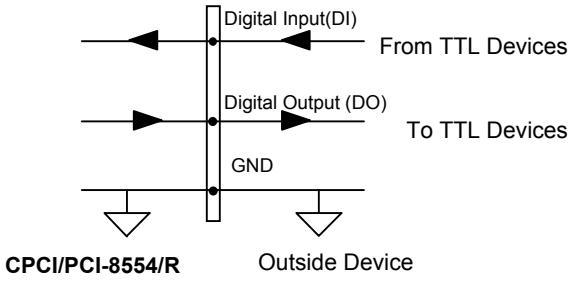
Figure 19: Digital I/O Connection
# 4.3 Timer/Counter Connection
The cPCI/PCI-8554/R has four 8254 chips on board. It can offer 10 independent 16-bit programmable down counters with the option of cascading the counters. To implement your application, the following procedures should be followed.
1. Does the application require a fixed frequency, if answer is ‘No’, an external clock source must be used. Go to step 3.
2. Calculate the frequency of the clock according to your application requirements, then decide which clock source to use (internal, external, or cascaded), and then decide which counters to use.
3. If an external clock source is chosen, generate a clock signal external to the cPCI/PCI-8554/R card and measure its frequency. Determine whether the debounce function should be enabled or disabled, and then set JP1 \~ JP10. If reserved counters 11 and 12 are required, set JP12 and JP13 to pin 2-3.
4. Decide the gate control source: always enable or external controls, if gate control is necessary, connect the gate signal.
Note: Gate control of counter 11 and 12 are always enabled (tied to logic high) and there are no gate control pins for counters 11 and 12 on CN1.
5. Program the counter/timer using the desired mode.
# 4.4 Frequency Generator
# 4.4.1 To generate a 250 KHz Square Wave.
Step 1: Use a fixed clock source because the output is a fixed frequency.
Step 2: The internal 8MHz clock is capable of generating the 250KHz frequency. Use Counter 1 for this application.
$$
\therefore 2 5 0 \mathrm{kHz} = 8 \mathrm{MHz} / 3 2
$$
Step 3: The gate source should be set to “enable” always and therefore GATE1 is let open (pin 99 of CN1).
Step 4: Connect the counter output to an external device and write the control program. Refer to ‘DEMO1.C’ source code.
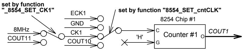
Figure 20: Example of a frequency generator (1)
# 4.4.2 To generate a 1 pulse/1 hour signal
Step 1: Use a fixed clock source because the output is a fixed frequency.
Step 2: As the desired frequency is too slow, one counter will be unable to produce the desired frequency (1/3600sec=0.000278Hz. Therefore to reach this low frequency, cascade the independent counters 1, 2 and 3. Set the clock source of counter 1 to the internal 8MHz. Connect COUT1 to clock source of counter 2, and connect COUT2 to clock source of counter 3.
Step 3: Using the counter divider function, set counter 1 to 4000, counter 2 to 2000, and counter 3 to 3600.
$$
\therefore 8 \mathrm{MHz} / 4 0 0 0 / 2 0 0 0 / 3 6 0 0 = 1 / 3 6 0 0,
$$
Hence COUT3 will generate a pulse every hour.
Step 4: The gate sources to enable always, hence GATE1, GATE2, and GATE3 are open.
Step 5: Write and verify the control program. Refer to ‘DEMO2.C’ source code.
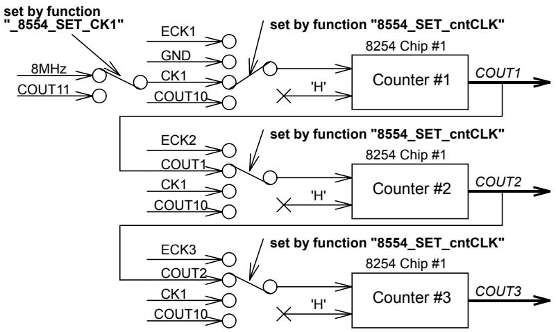
Figure 21: Example of frequency generator (2)
# 4.5 Pulse Width Measurement
Step 1: Use a fixed clock source as base time interval (or base frequency).
Step 2: Assuming an internal 2MHz clock is used. The time base is:
$$
\Delta t = 1 / 2 \mathrm{M} = 5 \times 1 0 \mathrm{e} - 7 \sec
$$
The count range for measuring the pulse width is:
$$
\Delta t < \text { pulse width } < \Delta t * 6 5 5 3 5 (= 3 2. 7 6 8 \mathrm{msec})
$$
If the specification of the pulse width to be measured is within the range, the 2MHz can be used. Otherwise change the base frequency of the counter, for example, you can set counter 2 to cascaded mode, and use counter 2 to measure the pulse width. The count range will increase but the resolution will decrease. Counter 1, 2, and 3 are used in this example.
Step 3: Connect GATE1 to the signal to be measured.
Step 4: Write and verify the control program. Refer to ‘DEMO3.C’ source code.
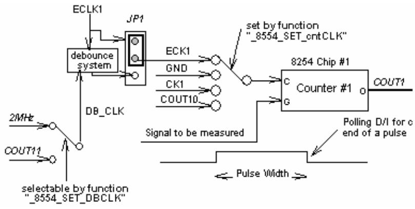
Figure 22: Example of pulse width measurement
# 4.6 Frequency Measurement
To measure a frequency around 1\~100 KHz the following steps can be followed.
Step 1: This application requires two counters. One counter is used to generate a pulse with a precise time interval. The pulse is then used to enable the second counter (Counting counter). In this example the gate control is from COUT3 and cascaded counters configuration is used. The pulse generator is set to counter 3 (clock from COUT2) and counter 1 is used to measure the frequency.
Step 2: The maximum value of the counting counter is 65535. To measure a 100 KHz signal, the time interval must be within 1/100 KHz x 65535 = 0.655 seconds. If the time interval is wider, then the measurement resolution is better, however, the counting value will overflow if the time interval is too large. This means the low pulse width for counter 3 output should be shorter than 0.655 sec.
Step 3: Connect the signal to be measured to ECLK1 and adjust JP1 to allow the debounce function.
Step 4: Connect GATE1 to /COUT3.
Step 5: The following block diagram illustrates the application. Write and verify the control program. The frequency of the signal is:
Frequency = Counting value of counter 1/precise time interval
Refer to ‘DEMO4.C’ source code.
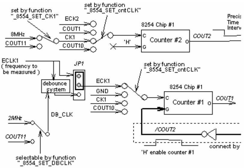
Figure 23: Example of frequency measurement (1)
# 4.7 Event Counter
This example counts how many external events in 1 second
Step 1: This application requires one counter to generate a time base of 1 second and the second counter to count the event. Cascaded counters 11and 12 are used as a watchdog timer. Counter 1 is used in this example to count the external events. The clock source of counter 1 is the event signal so the frequency is not fixed.
Step 2: Connect ECLK1 to the signal to be measured and adjust JP1 to enable the debounce function.
Step 4: The gate source of counter 1 is always enabled, so the external gate is open.
Step 5: Write the control program. Refer to‘DEMO5.C’ source code.
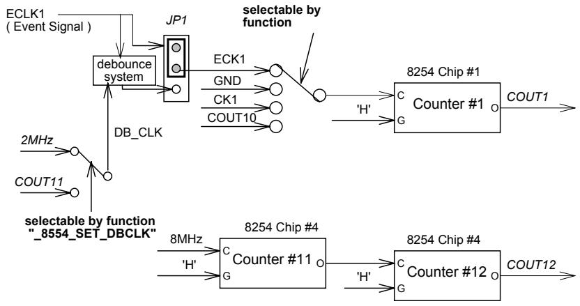
Figure 24: Example of event counter
# 4.8 Dual Interrupt System
The cPCI/PCI-8554/R provides a dual interrupt source (one internal plus one external), which can be very useful in some applications. For example, most applications require a watchdog timer to monitor the system periodically; hence, an IRQ channel is used. An emergency control may also be necessary; therefore the external IRQ channel will come in handy.
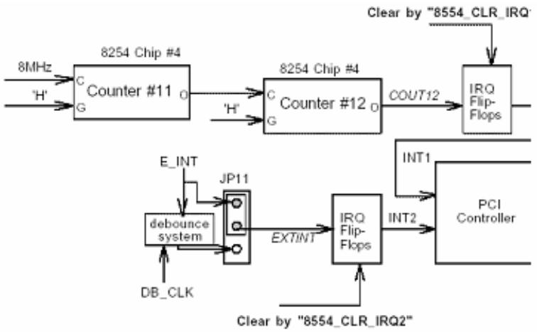
Figure 25: Example of dual interrupt system
# 5
# C/C++ Library
This chapter describes the software libraries for operating this card. Only the functions in the DOS library and Windows 95 DLL are described. Refer to the PCIS-DASK function reference manual, which is included in the ADLINK CD, for descriptions of Windows 98/NT/2000 DLL functions.
The function prototypes and useful constants are defined in the header files located in the LIB directory (DOS) and INCLUDE directory (Windows 95). For Windows 95 DLL, the developing environment can be Visual Basic 4.0 or above, Visual C/C++ 4.0 or above, Borland C++ 5.0 or above, Borland Delphi 2.x (32-bit) or above, or any Windows programming language that allows calls to a DLL.
# 5.1 Libraries Installation
Refer to the “Software Installation Guide” for information regarding software installation of libraries for DOS, Windows 95 DLL, or PCIS-DASK for Windows 98/NT/2000.
The device drivers and DLL functions for Windows 98/NT/2000 are included in the PCIS-DASK. Refer to the PCIS-DASK user’s guide and function reference, which is included in the ADLINK CD, for programming information.
# 5.2 Programming Guide
# 5.2.1 Naming Convention
The functions of the NuDAQ PCI or NuIPC CompactPCI card software drivers uses full-names to represent the functions' real meaning. The naming convention rules are:
# In DOS Environment:
$\mathtt { \_ { ( h a r d w a r e \_ m o d e l ) \_ ( a c t i o n \_ n a m e ) . e . g . \_ 8 5 5 4 \_ l n i t i a l ( \lambda ) . } }$
In order to recognize the difference between the DOS library and Windows 95 library, a capital "W" is placed at the start of each function name for Windows 95 DLL drivers. e.g. W\_8554\_Initial().
# 5.2.2 Data Types
We have defined some data types in the Pci\_8554.h (DOS) and Acl\_pci.h (Windows 95) header files. These data types are used by the NuDAQ Cards’ library. We recommend you use these data types in your application programs. The following table shows the data type names and their range.
<table>| Type Name | Description | Range |
| U8 | 8-bit ASCII character | 0 to 255 |
| I16 | 16-bit signed integer | -32768 to 32767 |
| U16 | 16-bit unsigned integer | 0 to 65535 |
| I32 | 32-bit signed integer | -2147483648 to 2147483647 |
| U32 | 32-bit single-precision floating-point | 0 to 4294967295 |
| F32 | 32-bit single-precision floating-point | -3.402823E38 to 3.402823E38 |
| F64 | 64-bit double-precision floating-point | -1.797683134862315E308 to 1.797683134862315E309 |
| Boolean | Boolean logic value | TRUE, FALSE |
Table 9. Data types and their ranges
# 5.3 \_8554\_Initial
# @ Description
The cPCI/PCI-8554/R cards are initialized by this function. The software library could be used to control multiple cPCI/PCI-8554/R cards. Because the cPCI/PCI-8554/R is designed with the PCI bus architecture and meets the plug and play specifications, the IRQ and I/O address are assigned by system BIOS directly.
# @ Syntax
C/C++ (DOS)
U16 \_8554\_Initial (U16 \*existCards, PCI\_INFO \*pciinfo)
C/C++ (Windows 95)
U16 W\_8554\_Initial (U16 \*existCards, PCI\_INFO \*pciinfo)
# Visual Basic (Windows 95)
W\_8554\_Initial (existCards As Integer, pciInfo As PCI\_INFO) As Integer
# @ Arguments
existCards:
The numbers of installed cPCI/PCI-8554/R cards. The returned value shows how many cPCI/PCI-8554/R cards are installed in the system.
pciinfo:
This structure stores the PCI bus plug and play initialization information, which is determined by PnP BIOS. The PCI\_INFO structure is defined in the PCI\_8554.H header file. The base I/O address and the interrupt channel number is stored in pciinfo for reference.
# @ Return Value
ERR\_NoError, ERR\_PCIBiosNotExist
# 5.4 \_8554\_Write\_Counter
# @ Description
User can directly write commands to counters 1\~12 using this function. Using this function, user can also re-assign the counter numbers 1\~12 in any order
# @ Syntax
C/C++ (DOS)
U16 \_8554\_Write\_Counter (U16 cardNo, U16 cntNo, U16 mode, U16 cntrVal)
C/C++ (Windows 95)
U16 W\_8554\_Write\_Counter (U16 cardNo, U16 cntNo, U16 mode, U16 cntrVal)
# Visual Basic (Windows 95)
W\_8554\_Write\_Counter (ByVal cardNo As Integer, ByVal cntNo As Integer, ByVal mode As Integer, ByVal cntrVal As Integer) As Integer
# @ Arguments
cardNo: card number to be selected
cntNo: Counter/Timer number. This value must be between 1 and 12.
mode: Counter operation mode. This value must be between 0 and 5.
cntrVal: The counter value to be written to the counter.
# @ Return Value
ERR\_NoError
ERR\_BoardNoInit
ERR\_InvalidCounterNo: cntNo is out of range.
ERR\_TimerMode: mode is out of range
# 5.5 \_8554\_Read\_Counter
@ Description
User can directly read counter information with this function.
@ Syntax
```txt
C/C++ (DOS)
```
```csv
U16 _8554_Read_Counter (U16 cardNo, U16 cntNo, U16 *mode, U16 *cntrVal)
```
```txt
C/C++ (Windows 95)
```
```txt
U16 W_8554_Read_Counter (U16 cardNo, U16 cntNo, U16 *mode, U16 *cntrVal)
```
# Visual Basic (Windows 95)
W\_8554\_Read\_Counter (ByVal cardNo As Integer, ByVal cntNo As Integer, mode As Integer, cntrVal As Integer) As Integer
@ Arguments
cardNo: card number to be selected
cntNo: Counter/Timer number. This value must be between 1 and 12.
mode: Counter operation mode.
cntrVal: Counter value read back from counter
@ Return Value
ERR\_NoError, ERR\_BoardNoInit
ERR\_InvalidCounterNo: cntNo is out of range.
# 5.6 \_8554\_Stop\_Counter
# @ Description
User can directly stop the counter with this function. This function will stop the counter by setting the counter to mode 5.
# @ Syntax
```txt
C/C++ (DOS)
```
U16 \_8554\_Stop\_Counter (U16 cardNo,U16 cntNo,U16 \*cntrVal)
```txt
C/C++ (Windows 95)
```
U16 W\_8554\_Stop\_Counter (U16 cardNo,U16 cntNo,U16 \*cntrVal)
# Visual Basic (Windows 95)
W\_8554\_Stop\_Counter (ByVal cardNo As Integer, ByVal cntNo As Integer, cntrVal As Integer) As Integer
# @ Arguments
cardNo: card number to be selected
cntNo: Counter/Timer number. This value must be between 1 and 12.
cntrVal: Counter value read back from counter
# @ Return Value
ERR\_NoError , ERR\_BoardNoInit
ERR\_InvalidCounterNo: if cntNo is not in the range of 1 \~ 12
# 5.7 \_8554\_Read\_Status
@ Description
User can directly read current counter status with this function.
@ Syntax
C/C++ (DOS)
U16 \_8554\_Read\_Status (U16 cardNo, U16 cntNo, U16 \* cntrVal, U16 \*status)
C/C++ (Windows 95)
U16 W\_8554\_ Read\_Status (U16 cardNo, U16 cntNo, U16 \* cntrVal, U16 \*status)
Visual Basic (Windows 95)
W\_8554\_Read\_Status (ByVal cardNo As Integer, ByVal cntNo As Integer, cntrVal As Integer, status As Integer) As Integer
@ Arguments
cardNo: card number to be selected
cntNo: Counter/Timer number. This value must be between 1 and 12.
cntrVal: Counter value read back from counter
status: current status read back from counter, refer to 8254’s datasheet for more information
@ Return Value
ERR\_NoError, ERR\_BoardNoInit
ERR\_InvalidCounterNo: if cntNo is not in the range of 1 \~ 12
# 5.8 \_8554\_DO
@ Description
Write an 8-bit data to the digital output port.
@ Syntax
C/C++ (DOS)
U16 \_8554\_DO (U16 cardNo, U16 doData)
C/C++ (Windows 95)
U16 W\_8554\_DO (U16 cardNo, U16 doData)
Visual Basic (Windows 95)
W\_8554\_DO (ByVal cardNo As Integer, ByVal doData As Integer) As Integer
@ Arguments
cardNo: card number to be selected
doData: the value to be written to digital output port
@ Return Value
ERR\_NoError
ERR\_PCIBiosNotExist
# 5.9 \_8554\_DI
@ Description
Read an 8-bit data from the digital input port.
@ Syntax
C/C++ (DOS)
U16 \_8554\_DI (U16 cardNo, U16 \*diData)
C/C++ (Windows 95)
U16 W\_8554\_DI (U16 cardNo, U16 \*diData)
Visual Basic (Windows 95)
W\_8554\_DI (ByVal cardNo As Integer, diData As Integer) As Integer
@ Arguments
cardNo: card number to be selected
doData: the value read from the digital input port
@ Return Value
ERR\_NoError, ERR\_BoardNoInit
# 5.10 \_8554\_SET\_cntCLK
# @ Description
This function is used to select the clock source for counters 1\~10 (Clock source for counter 11 is 8MHz and clock source of counter 12 is from COUT11, both clock sources are fixed).
# @ Syntax
C/C++ (DOS)
U16 \_8554\_DI (U16 cardNo, U16 cntNo, U16 clkMODE)
C/C++ (Windows 95)
U16 W\_8554\_DI (U16 cardNo, U16 cntNo, U16 clkMODE)
# Visual Basic (Windows 95)
W\_8554\_SET\_cntCLK (ByVal cardNo As Integer, ByVal cntNo As Integer, ByVal clkMODE As Integer) As Integer
# @ Arguments
cardNo: card number to be selected
cntNo: Counter/Timer number. This value must be between 1 and 10.
clkMODE: Select clock sources:
$$
" 0" = \text { ECLKn }.
$$
$$
" 1" = \text { COUTn - 1 }.
$$
$$
" 2" = \mathrm{CK1}.
$$
$$
" 3" = \text { COUT10 }.
$$
# @ Return Value
ERR\_NoError
ERR\_BoardNoInit
ERR\_InvalidCounterNo: cntNo is not in the range of 1 \~ 12
ERR\_InvalidMode: clkMODE is not in the range of 0 \~ 3
# 5.11 \_8554\_SET\_CK1
@ Description
Select source for CK1.
@ Syntax
C/C++ (DOS)
U16 \_8554\_SET\_CK1 (U16 cardNo, U16 selCK1)
C/C++ (Windows 95)
U16 W\_8554\_SET\_CK1 (U16 cardNo, U16 selCK1)
Visual Basic (Windows 95)
W\_8554\_SET\_CK1 (ByVal cardNo As Integer, ByVal selCK1 As Integer) As Integer
@ Arguments
cardNo: card number to be selected
selCK1: if selCK1 is set to “0” then CK1 = C8M, and if set to “1” then CK1 = COUT11
@ Return Value
ERR\_NoError
ERR\_BoardNoInit
ERR\_InvalidMode: selCK1 is out of range
# 5.12 \_8554\_SET\_DBCLK
@ Description
Select debounce clock.
@ Syntax
C/C++ (DOS)
U16 \_8554\_SET\_DBCLK (U16 cardNo, U16 DBCLK)
C/C++ (Windows 95)
U16 W\_8554\_SET\_DBCLK (U16 cardNo, U16 DBCLK)
Visual Basic (Windows 95)
W\_8554\_SET\_DBCLK (ByVal cardNo As Integer, ByVal DBCLK As Integer) As Integer
@ Arguments
cardNo: card number to be selected
DBCLK: if dbclk is set to “0” then DB\_CLK = COUT11, and if set to “1” then DB\_CLK = 2MHz
@ Return Value
ERR\_NoErro, ERR\_BoardNoInit
ERR\_InvalidMode: DBCLK is out of range
# 5.13 \_8554\_Set\_INT\_Control
# @ Description
The cPCI/PCI-8554/R has a dual interrupts system. Two interrupt sources can be generated and be checked by the software. This function is used to select and control the cPCI/PCI-8554/R interrupt sources. The interrupt source can either come from counter 12’s output, COUT12 (INT1) or from an external interrupt signal EXTINT (INT2).
# @ Syntax
C/C++ (DOS)
U16 \_8554\_Set\_INT\_Control (U16 cardNo, U16 int1Flag, U16 int2Flag)
C/C++ (Windows 95)
U16 W\_8554\_Set\_INT\_Control (U16 cardNo, U16 int1Flag, U16 int2Flag)
# Visual Basic (Windows 95)
W\_8554\_Set\_INT\_Control (ByVal cardNo As Integer, ByVal int1Falg As Integer, ByVal int2Falg As Integer)
# @ Arguments
cardNo: card number to be selected
int1Flag: INT1 setting; 0: disable, 1: enable
int2Flag: INT2 setting; 0: disable, 1: enable
# 5.14 \_8554\_Get\_IRQ\_Status
# @ Description
The cPCI/PCI-8554/R has dual interrupts system. Two interrupt sources can be generated and be checked by the software. This function is used to distinguish which interrupt has been inserted if both INT1 and INT2 interrupts are used.
# @ Syntax
```txt
C/C++ (DOS)
```
U16 \_8554\_Get\_IRQ\_Status (U16 cardNo, U16 \*ch1, U16 \*ch2)
```txt
C/C++ (Windows 95)
```
U16 W\_8554\_Get\_IRQ\_Status (U16 cardNo, U16 \*ch1, U16 \*ch2)
# Visual Basic (Windows 95)
W\_8554\_Get\_IRQ\_Status (ByVal cardNo As Integer, ch1 As Integer, ch2 As Integer)
# @ Arguments
cardNo: card number to be selected
ch1: INT1 status; 0: interrupt is not from INT1, 1: interrupt is from INT1
ch2: INT2 status; 0: interrupt is not from INT2, 1: interrupt is from INT2
# 5.15 \_8554\_INT\_Enable
# @ Description
This function is only available to the Windows 95 driver. It is used to activate the interrupt controller. After calling this function, every time an interrupt request signal is generated, a software event is signaled.
# @ Syntax
C/C++ (Windows 95)
U16 W\_8554\_INT\_Enable (U16 cardNo, HANDLE \*hEvent)
# Visual Basic (Windows 95)
W\_8554\_INT\_Enable (ByVal cardNo As Integer, hEvent As Long) As Integer
# @ Arguments
cardNo: card number to be selected
hEvent: the address of an array for two handles. HEvent[0] and hEvent[1] are the events for interrupt signals INT1 and INT2 respectively.
# @ Return Value
ERR\_NoError
ERR\_BoardNoInit
# 5.16 \_8554\_INT\_Disable
@ Description
This function is only available to the Windows 95 driver. It is used to disable the generation of an interrupt signal.
@ Syntax
C/C++ (Windows 95)
U16 W\_8554\_INT\_Disable (U16 cardNo)
Visual Basic (Windows 95)
W\_8554\_INT\_Disable (ByVal cardNo As Integer) As Integer
@ Arguments
cardNo: card number to be selected
@ Return Value
ERR\_NoError, ERR\_BoardNoInit
# 5.17 \_8554\_CLR\_IRQ1
@ Description
This function is only available to the DOS driver. It is used to clear the interrupt request, which is generated by INT1. You should use this function to clear the interrupt request status; otherwise the new incoming interrupt will not be generated.
@ Syntax
C/C++ (Windows 95)
U16 \_8554\_CLR\_IRQ1 (U16 cardNo)
@ Arguments
cardNo: card number to be selected
# 5.18 \_8554\_CLR\_IRQ2
# @ Description
This function is only available to the DOS driver. It is used to clear the interrupt request, which is generated by INT2. You should use this function to clear the interrupt request status; otherwise the new incoming interrupt will not be generated.
# @ Syntax
C/C++ (Windows 95)
U16 \_8554\_CLR\_IRQ2 (U16 cardNo)
# @ Arguments
cardNo: card number to be selected
# Warranty Policy
Thank you for choosing ADLINK. To understand your rights and enjoy all the after-sales services we offer, please read the following carefully.
1. Before using ADLINK’s products please read the user manual and follow the instructions exactly. When sending in damaged products for repair, please attach an RMA application form which can be downloaded from: http://rma.adlinktech.com/policy/.
2. All ADLINK products come with a limited two-year warranty, one year for products bought in China.
The warranty period starts on the day the product is shipped from ADLINK’s factory.
Peripherals and third-party products not manufactured by ADLINK will be covered by the original manufacturers' warranty.
For products containing storage devices (hard drives, flash cards, etc.), please back up your data before sending them for repair. ADLINK is not responsible for any loss of data.
Please ensure the use of properly licensed software with our systems. ADLINK does not condone the use of pirated software and will not service systems using such software. ADLINK will not be held legally responsible for products shipped with unlicensed software installed by the user.
For general repairs, please do not include peripheral accessories. If peripherals need to be included, be certain to specify which items you sent on the RMA Request & Confirmation Form. ADLINK is not responsible for items not listed on the RMA Request & Confirmation Form.
3. Our repair service is not covered by ADLINK's guarantee in the following situations:
Damage caused by not following instructions in the User's Manual.
Damage caused by carelessness on the user's part during product transportation.
Damage caused by fire, earthquakes, floods, lightening, pollution, other acts of God, and/or incorrect usage of voltage transformers.
Damage caused by inappropriate storage environments such as with high temperatures, high humidity, or volatile chemicals.
Damage caused by leakage of battery fluid during or after change of batteries by customer/user.
Damage from improper repair by unauthorized ADLINK technicians.
Products with altered and/or damaged serial numbers are not entitled to our service.
This warranty is not transferable or extendible.
Other categories not protected under our warranty.
4. Customers are responsible for all fees necessary to transport damaged products to ADLINK.
For further questions, please e-mail our FAE staff: service@adlinktech.com
[🔗 Link to the original document](.cpci-8554-r-manual-4-en/cpci-8554-r-manual-4-en.pdf)