# cPCI-A3525 Series

Performance 3U CompactPCI® Serial 9th Gen Intel® Core™ / Intel® Xeon® Processor Blade

User’s Manual

![Close-up of an electronic circuit board with internal components and connectors (no visible text or symbols)](.cpci-a3525-50m-65320-1010-11/a47a4cd0f9bf5a8c0c8ed69992f02a1447297d4cd8ba63fe0da9eeec3512930d.jpg)

Manual Rev.: 1.1

Revision Date: May 14, 2025

Part No: 50M-65320-1010

Revision History

<table><tr><td>Revision</td><td>Release Date</td><td>Description of Change(s)</td></tr><tr><td>1.0</td><td>2023-08-08</td><td>Initial release</td></tr><tr><td>1.1</td><td>2025-05-14</td><td>Note regarding Intel PCH and PCIe specifications added</td></tr></table>

# Preface

# Copyright © 2025 ADLINK Technology Inc.

This document contains proprietary information protected by copyright. All rights are reserved. No part of this manual may be reproduced by any mechanical, electronic, or other means in any form without prior written permission of the manufacturer.

# Disclaimer

The information in this document is subject to change without prior notice in order to improve reliability, design, and function and does not represent a commitment on the part of the manufacturer.

In no event will the manufacturer be liable for direct, indirect, special, incidental, or consequential damages arising out of the use or inability to use the product or documentation, even if advised of the possibility of such damages.

# Environmental Responsibility

ADLINK is committed to fulfill its social responsibility to global environmental preservation through compliance with the European Union's Restriction of Hazardous Substances (RoHS) directive and Waste Electrical and Electronic Equipment (WEEE) directive. Environmental protection is a top priority for ADLINK. We have enforced measures to ensure that our products, manufacturing processes, components, and raw materials have as little impact on the environment as possible. When products are at their end of life, our customers are encouraged to dispose of them in accordance with the product disposal and/or recovery programs prescribed by their nation or company.

![Symbol of a trash bin crossed with a diagonal line, no text or labels present](.cpci-a3525-50m-65320-1010-11/860849031070ec915cad94c2fe2a8e84bf37ef9e08f57967797f29452c2fe47c.jpg)

Battery Labels
![Symbol of a trash bin crossed out by two diagonal lines (no text or labels)](.cpci-a3525-50m-65320-1010-11/41a97648895c36f5fa73d5d268d208d9bc4067ee4054ddbecd915e53c6b12641.jpg)

![Recycling symbol icon with three chasing arrows inside a square frame (no text or labels)](.cpci-a3525-50m-65320-1010-11/379fd1ebe4cf38bca78ae7a333809dfc758bf1c7a33f8c5d66a483229345b5fe.jpg)

Li-ion

![RECYCLE\nRBRC\nLi-ion\n7.800.822.8837](.cpci-a3525-50m-65320-1010-11/aec46078dd69c0863689d7c77a66c4e55e58f80c4fcd04f1a7bdc361ccb41d31.jpg)

![Abstract geometric pattern with interlocking black and white shapes (no text or symbols)](.cpci-a3525-50m-65320-1010-11/4ba71b073f5ae421eef01ca45cf4bb4793cdf7ae53aa968a92ac71945277ea02.jpg)

ᑜ㔚ᳰ⺧࿁ᡴ

# California Proposition 65 Warning

![The image displays a standard warning symbol consisting of a yellow equilateral triangle with a thick black border. Centered inside the triangle is a large black exclamation point.](.cpci-a3525-50m-65320-1010-11/abdf26d02f8b7b5fd7806e7675cdf257181f30f314c2d240dfe73161c9f41733.jpg)

WARNING: This product can expose you to chemicals including acrylamide, arsenic, benzene, cadmium, Tris(1,3-dichloro-2-propyl) phosphate (TDCPP),

1,4-Dioxane, formaldehyde, lead, DEHP, styrene, DINP, BBP, PVC, and vinyl materials, which are known to the State of California to cause cancer, and acrylamide, benzene, cadmium, lead, mercury, phthalates, toluene, DEHP, DIDP, DnHP, DBP, BBP, PVC, and vinyl materials, which are known to the State of California to cause birth defects or other reproductive harm. For more information go to www.P65Warnings.ca.gov.

# Trademarks

Product names mentioned herein are used for identification purposes only and may be trademarks and/or registered trademarks of their respective companies.

# Conventions

Take note of the following conventions used throughout this manual to make sure that users perform certain tasks and instructions properly.

![A white document icon featuring a folded upper-right corner and faint horizontal lines, overlaid with a large red checkmark.](.cpci-a3525-50m-65320-1010-11/b641f45e769e505e0df704fecbc3eac5b3d63c18fe9b9f04b6d46471d1530acc.jpg)
NOTE:

Additional information, aids, and tips that help users perform tasks.

![The image displays a standard warning sign featuring a yellow equilateral triangle with a thick black border. Centered within the triangle is a large black exclamation point.](.cpci-a3525-50m-65320-1010-11/6e96428eaa8efc51d444ba078dc9078345055211184989d666d9f39abefe2df1.jpg)
CAUTION:

Information to prevent minor physical injury, component damage, data loss, and/or program corruption when trying to complete a task.

![The image displays a standard red triangular warning sign with a thin white border. Inside the red triangle, there is a large, white exclamation point centered vertically and horizontally.](.cpci-a3525-50m-65320-1010-11/2120319fb5d58a00b34fab36e1310f0c011473c903a7f7e66a27737313c76577.jpg)
WARNING:

Information to prevent serious physical injury, component damage, data loss, and/or program corruption when trying to complete a specific task.

# Table of Contents

# Revision History.......... ii

# Preface ............ iii

# List of Figures ........ ix

# List of Tables ........ . xi

# 1 Introduction .........

1.1 Overview... 1
1.2 Features... 2
1.3 Model Number Decoder.... 3
1.4 Package Contents . 4

# 2 Specifications ........ 5

2.1 cPCI-A3525 Processor Blade Specifications.. 5
2.2 Block Diagrams.. 7
2.3 I/O Connectivity Table . 8
2.4 Power Requirements .... 9

# 3 Board Interfaces ........ 11

3.1 cPCI-A3525 Series Board Layout.. 11
3.2 cPCI-A3525 Blade Assembly Layout.. 1 2
3.3 cPCI-A3525 Faceplate... 13
3.4 cPCI-A3525 Rear Signal Distribution.... 15
3.5 Connector Pin Assignments ..... 16

# 4 Getting Started ........ 2 3

4.1 CPU and Heatsink .. 23
4.2 Installing the cPCI-A3525 to the Chassis .. 2 4

# 5 Driver Installation ........ 25

5.1 cPCI-A3525 Drivers ... 25

# 6 Utilities ...... . 27

6.1 SEMA.. . 27
6.2 Preboot Execution Environment (PXE)...... 2 7
6.3 Watchdog Timer... 28
6.4 General Purpose LED Control .. 30

# 7 BIOS Setup Utility .......... .. 33

7.1 Starting the BIOS .. 33
7.2 Main Setup...... . 35

7.2.1 BIOS Information .. 36
7.2.2 System Information.... .. 36
7.2.3 Board Information .... .. 36
7.2.4 System Date and Time .. . 37

7.3 Advanced.. 38

7.3.1 CPU Configuration..... .. 38
7.3.2 Power Management . .. 39
7.3.3 USB Configuration ..... .. 40
7.3.4 AMT Configuration..... .. 41
7.3.5 System Management. .. 41
7.3.6 Thermal Management.. .. 43
7.3.7 Watchdog Timer .... .. 43
7.3.8 CSM Configuration .... .. 44
7.3.9 Miscellaneous . . 44
7.3.10AMI Graphic Output Protocol Policy ...... .. 45
7.3.11Network Stack Configuration .... .. 45

7.4 Chipset.. 46

7.4.1 System Agent (SA) Configuration.... . 46
7.4.2 PCH-IO Configuration. .. 50

7.5 Security ... 56

7.5.1 Password Description . . 56

7.6 Boot .... 57
7.7 Save & Exit ... . 58

7.7.1 Reset Options.... .. 58

Important Safety Instructions ........ 5 9

Getting Service......... . 61

This page intentionally left blank.

# List of Figures

Figure 2-1: cPCI-A3525 Processor Blade Functional Block Diagram 7

Figure 3-1: cPCI-A3525 Series Board Layout (component side)..... 11

Figure 3-2: cPCI-A3525 Blade Assembly Layout.. . 12

Figure 3-3: cPCI-A3525 Faceplate Layout.. . 13

This page intentionally left blank.

# List of Tables

Table 2-1: cPCI-A3525 Processor Blade Specifications.. . 5
Table 2-2: cPCI-A3525 I/O Connectivity..... . 8
Table 3-1: cPCI-A3525 Faceplate System LED Descriptions......... 14
Table 3-2: cPCI-A3525 Rear Signal Distribution... . 15
Table 3-3: USB 2.0 Pin Definition . . 16
Table 3-4: USB 3.0 Pin Definition ... . 16
Table 3-5: DisplayPort Pin Definition ... . 17
Table 3-6: RJ-45 GbE Pin Definitions.. . 18
Table 3-7: LAN LED Status Definitions.. .. 18

This page intentionally left blank.

# 1 Introduction

# 1.1 Overview

CompactPCI® Serial (PICMG CPCI-S.0) is a new modular computer standard officially adopted by PICMG in 2011. The Compact-PCI Serial standard defines a completely new connector to support high-speed serial interfaces including PCI Express, SATA, USB and Ethernet. A CompactPCI Serial backplane has six high-speed connectors P1 to P6 on the system slot but only P1 is mandatory on peripheral slots, P2 to P6 being optional. A CompactPCI Serial system can comprise a total of nine blades (one system blade and eight peripheral I/O blades) through an Ethernet full mesh or single star architecture. The CompactPCI® Serial standard is the next-generation of the CompactPCI® specification and provides more flexibility and higher speed and bandwidth in modular system solutions.

The ADLINK cPCI-A3525 Series is a 3U CompactPCI Serial compatible processor blade with SO-DIMM DDR4-2666 ECC memory up to 64GB. The ADLINK cPCI-A3525 features a 8th/9th generation Intel® Core™ processor with Mobile Intel® CM246 PCH Chipset.

The cPCI-A3525 Series is a 3U CompactPCI Serial blade available in single-slot (4HP) form factors with optional daughter boards to provide extra storage and with 2 extra GbE port throught P6 to the rear backplane. Faceplate I/O on the single slot (4HP) includes 1x DP, 2x GbE and 2x USB 3.0 ports (these I/O are common to all versions).

Serial interfaces on the backplane connectors P1 to P5 include two PCI Express x8, one PCI Express x2, two PCI Express x4, three PCI Express x1, seven SATA 6Gb/s, two USB 3.0, and eight USB 2.0 ports. Additionally, the P6 connector supports two Gigabit Ethernet interfaces.

The cPCI-A3525 is a high-performance solution for transportation, factory automation, defense and other industrial applications that require superior data transfer capability and advanced computing power. The ADLINK cPCI-A3525 provides high manageability, supports Satellite mode operation as a standalone blade in peripheral slots, and Smart Embedded Management Agent (SEMA) for system health monitoring. In addition, with multiple operating system and board support package (BSP) support, users can build a reliable and high-performance industrial system with cPCI-A3525 Series.

# 1.2 Features

 3U CompactPCI Serial (PICMG CPCI-S.0) processor blade in 4HP width form factor
 9th generation Intel® Core™ Processor
 Graphics engine integrated in processor supporting independent displays with DirectX 12, OpenGL 4.5
 Dual channel DDR4-2666 SO-DIMM memory with ECC, up to 32GB
Backplane communication by PCI Express, USB 2.0/3.0, SATA, and Gigabit Ethernet
 Supports Satellite mode operation as a standalone blade in peripheral slots
 Supports SEMA for system health monitoring
 Storage: onboard SATA SSD

# 1.3 Model Number Decoder

<table><tr><td>cPCI-</td><td>EX</td><td>A3525</td><td>KR</td><td>/9850HL</td><td>/M16</td></tr><tr><td></td><td>(A)</td><td></td><td>(B)</td><td>(C)</td><td>(D)</td></tr></table>

# (A) Operating Temperature Code

 Blank = -20°C to +70°C
 EX= -40°C to +85°C (for CPUs with TDP below 37W only)

# (B) Configuration Code

 Blank = Single slot width, 1x DP, 2x GbE, 2x USB 3.0
 Other = ODM/OEM project code

# (C) CPU Code

 2276ML = Quad-core Intel® Xeon® 2276ML processor
 9850HL = Quad-core Intel® Core™ i7-9850HL processor

# (D) Memory Size Code

 M16 = 2x 8GB DDR4-2666 SO-DIMM SDRAM
 M32 = 2x 16GB DDR4-2666 SO-DIMMSDRAM

# (E) Storage Configuration Code

 Blank = Default without P6 daughter board
 S128 = Onboard soldered 128GB SSD with Dual GbE Port to P6 on daughter board
 S32 = Onboard soldered 32GB SSD with Dual GbE Port to P6 on daughter board

# 1.4 Package Contents

The cPCI-A3525 is packaged with the following components. If any of the following items are missing or damaged, retain the shipping carton and packing material and contact the dealer for inspection. Please obtain authorization before returning any product to ADLINK. The packing contents of cPCI-A3525 Series non-standard configurations will vary depending on customer requests.

# Processor Blade

 The cPCI-A3525 Series Processor Blade

 CPU and memory specifications will differ depending on options selected
 Thermal module is assembled on the board

![The image displays a digital icon of a white document or piece of paper featuring faint grey horizontal lines. A large, bold red checkmark is superimposed over the right side of the paper.](.cpci-a3525-50m-65320-1010-11/7271b26af1177c9cd50cd3a3a8793fdd505a43c8a34f082f311826a4ec5fbdb9.jpg)
NOTE:

The contents of non-standard cPCI-A3525 configurations may vary depending on the customer’s requirements.

# Optional Accessories

 DisplayPort to DVI adapter cable (P/N 30-01120-0000)
 DisplayPort to VGA adapter cable (P/N 30-01121-0000)
 DisplayPort to HDMI adapter cable (P/N 30-01119-0000)

![The image displays a yellow triangular warning sign with a black border featuring a black exclamation mark in the center. Below the sign, the word 'CAUTION:' is written in black capital letters.](.cpci-a3525-50m-65320-1010-11/57a11a565c47d4c06aae96d0bd8aadaed632e7029dc88004a4cdc6a16f349afa.jpg)

This product must be protected from static discharge and physical shock. Never remove any of the components except at a static-free workstation. Use the anti-static bag shipped with the product when putting the board on a surface. Wear an anti-static wrist strap properly grounded on one of the system's ESD ground jacks when installing or servicing system components.

# 2 Specifications

2.1 cPCI-A3525 Processor Blade Specifications

<table><tr><td>CompactPCIS.0 Standards</td><td>PICMG 2.0 CPCI-S.0 CompactPCI® Serial R1.0</td></tr><tr><td>Mechanical</td><td>Standard 3U CompactPCIBoard size: 100mm x 160mmSingle slot (4HP, 20.32mm)CompactPCI Serial P1 to P6 connectors (P6 on DB-P620 daughter board)</td></tr><tr><td>Processor</td><td>Intel® Xeon® 2276ML Processor 2.0 to 4.2 GHz, 12M Cache, 25W by TDPIntel® CoreTM i7-9850HE Processor 2.7 to 4.1 GHz, 9M Cache, 45W by TDPIntel® CoreTM i7-9850HL Processor 1.9 to 4.1 GHz, 9M Cache, 25W by TDPPassive heatsink</td></tr><tr><td>Chipset</td><td>Mobile Intel® CM246 Chipset</td></tr><tr><td>Memory</td><td>Dual channel DDR4-2666 ECC SO-DIMM memory (Xeon® E-2276M)Dual channel DDR4-2666 SO-DIMM memory (CoreTM i7-9850HL)</td></tr><tr><td>BIOS</td><td>Dual AMI EFI BIOS, 128Mbit SPI flash memory</td></tr><tr><td>CompactPCI Bus</td><td>Support through CompactPCI bridge (cPCI-A3525B only1)PCI 32-bit, 33/66MHz; 3.3V, 5V universal V(IO)</td></tr><tr><td>Gigabit Ethernet</td><td>One PCIe x1 Intel® I219 GbE PHY and one PCIe x1 Intel® I210 Gigabit Ethernet controllersTwo egress 10/100/1000BASE-T ports on faceplateDual Gigabit Ethernet interfaces via P6 connector to backplane</td></tr><tr><td>Graphics</td><td>Integrated in Intel® processorDisplayPort outputs on faceplate with resolution up to 4096x2304 @60Hz</td></tr><tr><td>USB</td><td>Dual USB 3.0 ports on faceplate2x USB 3.0 to P1/P38x USB 2.0 to P1/P2/P3</td></tr><tr><td>PCI Express</td><td>2x PCIe 3.0 x8 to P1/P21x PCIe 2.0 x2 to P42x PCIe 2.0 x4 to P5</td></tr><tr><td>TPM</td><td>TPM 2.0 SLB 9665XT2.0 (upon request)</td></tr></table>

Table 2-1: cPCI-A3525 Processor Blade Specifications

<table><tr><td>Storage Interfaces</td><td>• Optional onboard up to 128GB SSD on daughter board• 7x SATA 6Gb/s to P3</td></tr><tr><td>Faceplate I/O</td><td>• 2x USB 3.0/2.0 ports• 2x 10/100/1000BASE-T Ethernet ports• 2x DisplayPort</td></tr><tr><td>OS Compatibility</td><td>• Microsoft Windows 10 64-bit</td></tr><tr><td>Environmental</td><td>• Operating Temperature (with forced air flow) $^{2}$ :Standard: -20°C to 70°CExtreme temperature: -40°C to +85°C(screened, by Intel cTDP and forced air flow)• Storage Temperature: -50°C to 100°C• Humidity: 95% @60°C non-condensing• Shock: 20G peak-to-peak, 11ms duration, operating• Vibration: 2Grms random vibration, 5-500Hz, each axis, operating</td></tr><tr><td>EMI</td><td>• CE EN55022• FCC Class A</td></tr></table>

Table 2-1: cPCI-A3525 Processor Blade Specifications

1. The cPCI-A3525B supporting CompactPCI bus requires a PICMG CPCI-S.0 backplane with system slot on the left and a PICMG 2.0 backplane with system slot on the right. Please contact your ADLINK representative for detailed information on compatible backplanes.
2. ADLINK-certified thermal design. The thermal performance is dependent on the chassis cooling design. Sufficient forced air-flow is required. Temperature limits of optional mass storage devices may also affect the thermal specification.
3. Due to Intel PCH specification limitations, the maximum number of PCIe Root Ports (or devices) that can be enabled at the same time is 16. The PCIe from PCH, peripheral slot 3 of the backplane, is effected when CPU slot is named as slot 0, while the PCIe from CPU, peripheral slots 1 and 2 are not effected.

# 2.2 Block Diagrams

# cPCI-A3525 Processor Blade
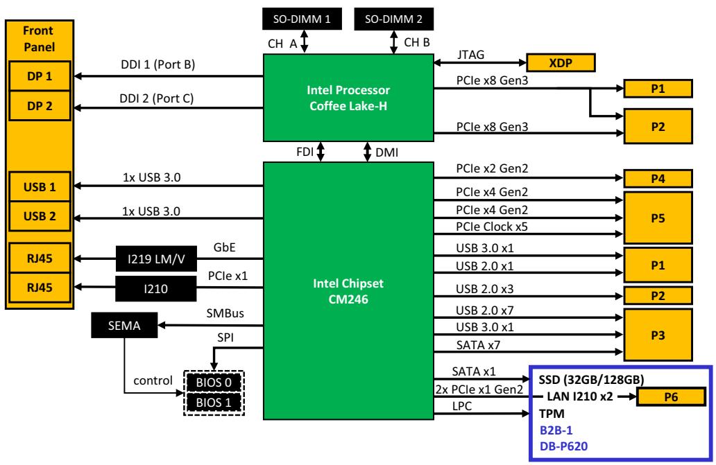
![**Blocks:**\n*   **Front Panel** (contains: **DP 1**, **DP 2**, **USB 1**, **USB 2**, **RJ45**, **RJ45**)\n*   **SO-DIMM 1**, **SO-DIMM 2**\n*   **Intel Processor Coffee Lake-H**\n*   **XDP**\n*   **P1**, **P2** (top right)\n*   **Intel Chipset CM246**\n*   **I219 LM/V**, **I210**\n*   **SEAMA**\n*   **BIOS 0**, **BIOS 1** (dashed box)\n*   **P4**, **P5**, **P1**, **P2**, **P3** (middle right)\n*   **Blue Box** (contains: **SSD (32GB/128GB)**, **LAN I210 x2**, **TPM**, **B2B-1**, **DB-P620**)\n*   **P6**\n\n**Connections:**\n*   **Front Panel** connects **DP 1** to **Intel Processor Coffee Lake-H** via **DDI 1 (Port B)** and **DP 2** via **DDI 2 (Port C)**.\n*   **Intel Processor Coffee Lake-H** connects to **SO-DIMM 1** via **CH A** and **SO-DIMM 2** via **CH B**.\n*   **Intel Processor Coffee Lake-H** connects to **XDP** via **JTAG** and to **P1** and **P2** via **PCIe x8 Gen3**.\n*   **Intel Processor Coffee Lake-H** connects to **Intel Chipset CM246** via **FDI** and **DMI**.\n*   **Front Panel** connects **USB 1** and **USB 2** to **Intel Chipset CM246** via **1x USB 3.0** each.\n*   One **RJ45** connects to **I219 LM/V**, which connects to **Intel Chipset CM246** via **GbE**. The other **RJ45** connects to **I210**, which connects to **Intel Chipset CM246** via **PCIe x1**.\n*   **Intel Chipset CM246** connects to **P4** via **PCIe x2 Gen2**.\n*   **Intel Chipset CM246** connects to **P5** via **PCIe x4 Gen2** (twice) and **PCIe Clock x5**.\n*   **Intel Chipset CM246** connects to **P1** via **USB 3.0 x1** and **USB 2.0 x1**.\n*   **Intel Chipset CM246** connects to **P2** via **USB 2.0 x3** and **USB 2.0 x7**.\n*   **Intel Chipset CM246** connects to **P3** via **USB 3.0 x1** and **SATA x7**.\n*   **Intel Chipset CM246** connects to the **Blue Box** via **SATA x1** to **SSD (32GB/128GB)**, **2x PCIe x1 Gen2** to **LAN I210 x2**, and **LPC** to **TPM**.\n*   **LAN I210 x2** connects to **P6**.\n*   **Intel Chipset CM246** connects to **SEAMA** via **SMBus** and to **BIOS 0** / **BIOS 1** via **SPI**.\n*   **SEAMA** connects to **BIOS 0** / **BIOS 1** via **control**.](.cpci-a3525-50m-65320-1010-11/7f1be1556e6d61dd60b20493e861a7a630f642b08f9298f30f1ce8cd2b664f35.jpg)

Figure 2-1: cPCI-A3525 Processor Blade Functional Block Diagram

# 2.3 I/O Connectivity Table

<table><tr><td rowspan="2">Function</td><td colspan="2">cPCI-A3525 (4HP)</td></tr><tr><td>Faceplate</td><td>Onboard</td></tr><tr><td>GbE</td><td>2 (RJ-45)</td><td>—</td></tr><tr><td>USB</td><td>2 (3.0)</td><td>—</td></tr><tr><td>Display</td><td>2 (DP)</td><td>—</td></tr><tr><td>Onboard SSD</td><td>—</td><td>1</td></tr></table>

Table 2-2: cPCI-A3525 I/O Connectivity

# 2.4 Power Requirements

In order to guarantee a stable functionality of the system, it is recommended to provide more power than the system requires. An industrial power supply unit should be able to provide at least twice as much power as the entire system requires of each voltage. An ATX power supply unit should be able to provide at least three times as much power as the entire system requires of each voltage.

# Power Consumption

This section provides information on the power consumption of cPCI-A3525 Series when using Intel® Core™ i7 processors with 16GB DDR4-2666 SO-DIMM memory and 2.5" SATA 256GB SATA SSD. The cPCI-A3525 is powered by +12V only.

<table><tr><td colspan="3">Intel® CoreTMi7-9850HE</td></tr><tr><td rowspan="2">OS/Mode</td><td>Current @12V</td><td>Total Power</td></tr><tr><td colspan="2">EIST Disabled / Enabled</td></tr><tr><td>Windows 10 x64 Idle Mode $^{1}$ </td><td>0.99A / 1.13A</td><td>11.88W / 13.5W</td></tr><tr><td>Windows 10 x64 Typical Mode $^{2}$ </td><td>3.65A / 4.82A</td><td>43.8W / 57.84W</td></tr><tr><td>Windows 10 x64 Maximum Mode $^{3}$ </td><td>4.08A / 4.94A</td><td>48.96W / 59.22W</td></tr></table>

<table><tr><td colspan="3">Intel® CoreTMi7-9850HL</td></tr><tr><td rowspan="2">OS/Mode</td><td>Current @12V</td><td>Total Power</td></tr><tr><td colspan="2">EIST Disabled / Enabled</td></tr><tr><td>Windows 10 x64 Idle Mode $^{1}$ </td><td>0.70A / 0.79A</td><td>8.40W / 9.48W</td></tr><tr><td>Windows 10 x64 Typical Mode $^{2}$ </td><td>3.43A / 3.63A</td><td>41.16W / 43.56W</td></tr><tr><td>Windows 10 x64 Maximum Mode $^{3}$ </td><td>3.58A / 3.76A</td><td>42.96W / 45.12W</td></tr></table>

1. The system set to idle mode and stays idle for 10 minutes.
2. Run BurnInTest™ that includes CPU, memory, video and 2D/3D graphics. Set all test items to 100% loading and run for 10 minutes.
3. Run Intel® Thermal Analysis Tool that includes CPU, graphics and memory. Set all test items to 100% loading and run for 10 minutes.

This page intentionally left blank.

# 3 Board Interfaces

This chapter illustrates the board layout, connector pin assignments, and jumper settings to familiarize users with the cPCI-A3525 Series.

# 3.1 cPCI-A3525 Series Board Layout

![DP1\nDIMM2\nDN3201\nDIMM1\nDP2\nBAT1\nUSB1\nUSB2\nLAN1\nCPU\nPCH\nP5\nP4\nP3\nP2\nP1](.cpci-a3525-50m-65320-1010-11/1c7a85342761de18b85d753d89cf85dc5efafa58d827f320a88f763809d2c0ff.jpg)

<table><tr><td>CPU</td><td>Intel® CoreTM Processor</td><td>P1-P5</td><td>CompactPCI Serial P1 to P5 connectors</td></tr><tr><td>PCH</td><td>Intel® CM246 Chipset</td><td>CN3201</td><td>Storage/Ethernet daughter board connector</td></tr><tr><td>BAT1</td><td>CMOS battery</td><td>DP1/2</td><td>DisplayPort connector</td></tr><tr><td>USB1/2</td><td>USB connectors</td><td>LAN1</td><td>Dual Ethernet connectors</td></tr><tr><td>DIMM1/2</td><td>DDR4 SO-DIMM Sockets</td><td colspan="2"></td></tr></table>

Figure 3-1: cPCI-A3525 Series Board Layout (component side)

# 3.2 cPCI-A3525 Blade Assembly Layout

This section describes the final assembly layout of the single slot cPCI-A3525 Blade.

![DB-P620\nP6\nAmphand\nAmphand](.cpci-a3525-50m-65320-1010-11/eee6eb81e9158a24982457ff55345e1cea93ce9151e72b42f6c161af34a83bfd.jpg)

Figure 3-2: cPCI-A3525 Blade Assembly Layout

<table><tr><td>DB-P620</td><td>Daughter board</td><td>P6</td><td>CompactPCI Serial P6 connector</td></tr></table>

# 3.3 cPCI-A3525 Faceplate

![USB 3.0\nGbE 1/2\nDisplayPort\nBIOS\nLoad\nDefault\nButton\nGP\nLED\nStorage\nLED\nPower\nLED\nThermal\nLED\nWDT\nLED\nReset\nButton](.cpci-a3525-50m-65320-1010-11/3a61621bde162875170b6b74f4d749e353cd23c93780c33b163488a792a0c830.jpg)

Figure 3-3: cPCI-A3525 Faceplate Layout

System LEDs

<table><tr><td>LED</td><td>Color</td><td>Condition</td><td>Indication</td></tr><tr><td rowspan="3">Power[CSXV]</td><td rowspan="3">Green/Red</td><td>Off</td><td>System is off</td></tr><tr><td>Red</td><td>System POST OK</td></tr><tr><td>Green</td><td>Power OK</td></tr><tr><td rowspan="2">WDT&lt;img src="images/e241c2af51038f68ee034b95f4310a0b937598ee9bb70acae64be4f02e528131.jpg"/&gt;</td><td rowspan="2">Amber</td><td>Off</td><td>No Watchdog event</td></tr><tr><td>Blinking</td><td>Watchdog event alert</td></tr><tr><td rowspan="2">Drive[12355]</td><td rowspan="2">Blue</td><td>Off</td><td>No SSD/mSATA/SATA drive activity</td></tr><tr><td>Blinking</td><td>Data read/write in process for SSD/ mSATA/SATA drive</td></tr><tr><td rowspan="2">Overheat&lt;img src="images/6b754e4a7b561f350e1fad4f498bc7fbe913e7713aeb3c66e9d61b0268d3d2ab.jpg"/&gt;</td><td rowspan="2">Red</td><td>Off</td><td>CPU temperature is under 95°C</td></tr><tr><td>Blinking</td><td>CPU temperature exceeds 95°C</td></tr><tr><td rowspan="2">GP(General Purpose)&lt;img src="images/47dde55bd2d8ed23420c9429c5b1ce41a941b66d2384839249e16c2fa5cc32fd.jpg"/&gt;</td><td rowspan="2">Yellow</td><td>Off</td><td>No activity</td></tr><tr><td>On/Blinking</td><td>Defined by user</td></tr></table>

Table 3-1: cPCI-A3525 Faceplate System LED Descriptions

![This image displays a white document icon featuring a folded top-left corner and faint horizontal lines. A large, bold red checkmark is superimposed diagonally across the document, indicating approval or verification.](.cpci-a3525-50m-65320-1010-11/6a32952e8d8d459b9eaf23af482578d1375a2accbfd399a387df037b23a66067.jpg)
NOTE:

The GP LED is connected to the GPIO pins of the BMC. The GP LED can be programmed by the user as a general purpose LED.

# 3.4 cPCI-A3525 Rear Signal Distribution

<table><tr><td>BP Slot</td><td>1 (System)</td><td>2</td><td>3</td><td>4</td><td>5</td><td>6</td><td>7</td><td>8</td><td>9</td></tr><tr><td>PCIe</td><td>1278</td><td>1 (x8)</td><td>2 (x8)</td><td>3(x2)</td><td>-</td><td>-</td><td>-</td><td>7 (x4)</td><td>8 (x4)</td></tr><tr><td>USB2</td><td>12345678</td><td>1</td><td>2</td><td>3</td><td>4</td><td>5</td><td>6</td><td>7</td><td>8</td></tr><tr><td>USB3</td><td>12</td><td>1</td><td>2</td><td></td><td></td><td>-</td><td>-</td><td>-</td><td>-</td></tr><tr><td>SATA</td><td>2345678</td><td>-</td><td>2</td><td>3</td><td>4</td><td>5</td><td>6</td><td>7</td><td>8</td></tr><tr><td>LAN</td><td>12</td><td>1*</td><td>2*</td><td>-</td><td>-</td><td>-</td><td>-</td><td>-</td><td>-</td></tr><tr><td>GA</td><td>-</td><td>7</td><td>6</td><td>5</td><td>4</td><td>3</td><td>2</td><td>1</td><td>0</td></tr></table>

Table 3-2: cPCI-A3525 Rear Signal Distribution

![The image shows a flat-style icon of a white document or page. The top-left corner is folded over. Faint horizontal lines run across the bottom half of the page, simulating text. A large, bold, red checkmark is superimposed over the center of the document, running diagonally upwards from left to right.](.cpci-a3525-50m-65320-1010-11/0c0804b5ef2ad298e0199245535ec4b1c6f9f8a4bb20c2862128d153be8dfaaa.jpg)
NOTE:

\*Supported by DB-P620 daughter board.

# 3.5 Connector Pin Assignments

# USB 2.0 Connectors

<table><tr><td>Pin #</td><td>Signal Name</td></tr><tr><td>1</td><td>Vcc</td></tr><tr><td>2</td><td>UV0-</td></tr><tr><td>3</td><td>UV0+</td></tr><tr><td>4</td><td>GND</td></tr></table>

![1\n2\n3\n4](.cpci-a3525-50m-65320-1010-11/643ad4010b788ad02dcf9255d477fa1b4405f653548b9d6c1136d51b48542514.jpg)

Table 3-3: USB 2.0 Pin Definition

# USB 3.0 Connectors

<table><tr><td>Pin #</td><td>Signal Name</td></tr><tr><td>1</td><td>USB3.0_P5VA</td></tr><tr><td>2</td><td>USB2_CMAN</td></tr><tr><td>3</td><td>USB2_CMAP</td></tr><tr><td>4</td><td>GND</td></tr><tr><td>5</td><td>USB3A_CMRXN</td></tr><tr><td>6</td><td>USB3A_CMRXP</td></tr><tr><td>7</td><td>GND</td></tr><tr><td>8</td><td>USB3A_CMTXN</td></tr><tr><td>9</td><td>USB3A_CMTXP</td></tr></table>

![1\n2\n3\n4\n5\n6\n7\n8\n9](.cpci-a3525-50m-65320-1010-11/a4bfad7bc0fb0fd1b206b89a19e33139f758ac2c5f1f2c947875479a97b25513.jpg)

Table 3-4: USB 3.0 Pin Definition

DisplayPort Connectors

<table><tr><td>Pin #</td><td>Signal</td><td>Pin #</td><td>Signal</td></tr><tr><td>1</td><td>CN_DP0_P</td><td>2</td><td>Ground</td></tr><tr><td>3</td><td>CN_DP0_N</td><td>4</td><td>CN_DP1_P</td></tr><tr><td>5</td><td>Ground</td><td>6</td><td>CN_DP1_N</td></tr><tr><td>7</td><td>CN_DP2_P</td><td>8</td><td>Ground</td></tr><tr><td>9</td><td>CN_DP2_N</td><td>10</td><td>CN_DP3_P</td></tr><tr><td>11</td><td>Ground</td><td>12</td><td>CN_DP3_N</td></tr><tr><td>13</td><td>CN_CAD-L</td><td>14</td><td>CN_CEC</td></tr><tr><td>15</td><td>CN_AUX_P</td><td>16</td><td>Ground</td></tr><tr><td>17</td><td>CN_AUX_N</td><td>18</td><td>DDP_HPD</td></tr><tr><td>19</td><td>Ground</td><td>20</td><td>P3V3</td></tr></table>

![1\n2\n19\n20](.cpci-a3525-50m-65320-1010-11/a8dcd7a262d3efb337d4c9eb22e5a1d16bd83e79ee768b7ab01145102420f830.jpg)

Table 3-5: DisplayPort Pin Definition

# RJ-45 Gigabit Ethernet Connectors

<table><tr><td>Pin #</td><td>10BASE-T/100BASE-TX</td><td>1000BASE-T</td></tr><tr><td>1</td><td>TX+</td><td>LAN_TX0+</td></tr><tr><td>2</td><td>TX-</td><td>LAN_TX0-</td></tr><tr><td>3</td><td>RX+</td><td>LAN_TX1+</td></tr><tr><td>4</td><td>—</td><td>LAN_TX2+</td></tr><tr><td>5</td><td>—</td><td>LAN_TX2-</td></tr><tr><td>6</td><td>RX-</td><td>LAN_TX1-</td></tr><tr><td>7</td><td>—</td><td>LAN_TX3+</td></tr><tr><td>8</td><td>—</td><td>LAN_TX3-</td></tr></table>

Table 3-6: RJ-45 GbE Pin Definitions

Speed Activity
![8\n1](.cpci-a3525-50m-65320-1010-11/2802e3b2586e27edd7424cecb91745fc4db5c4050268c9b907da18a634499b3a.jpg)

<table><tr><td colspan="2">Status</td><td>Speed LED (Green/Orange)</td><td>Activity LED (Yellow)</td></tr><tr><td colspan="2">Network link is not established or system powered off</td><td>OFF</td><td>OFF</td></tr><tr><td rowspan="2">10 Mbps</td><td>Link</td><td>OFF</td><td>ON</td></tr><tr><td>Active</td><td>OFF</td><td>Blinking</td></tr><tr><td rowspan="2">100 Mbps</td><td>Link</td><td>Green</td><td>ON</td></tr><tr><td>Active</td><td>Green</td><td>Blinking</td></tr><tr><td rowspan="2">1000 Mbps</td><td>Link</td><td>Orange</td><td>ON</td></tr><tr><td>Active</td><td>Orange</td><td>Blinking</td></tr></table>

Table 3-7: LAN LED Status Definitions

CompactPCI Serial Connector P1

<table><tr><td></td><td>A</td><td>B</td><td>C</td><td>D</td><td>E</td><td>F</td><td>G</td><td>H</td><td>I</td><td>J</td><td>K</td><td>L</td></tr><tr><td>6</td><td>GND</td><td>PEG_TX2_P</td><td>PEG_TX2_N</td><td>GND</td><td>PEG_RX2_P</td><td>PEG_RX2_N</td><td>GND</td><td>PEG_TX3_P</td><td>PEG_TX3_N</td><td>GND</td><td>PEG_RX3_P</td><td>PEG_RX3_N</td></tr><tr><td>5</td><td>PEG_TX0_P</td><td>PEG_TX0_N</td><td>GND</td><td>PEG_RX0_P</td><td>PEG_RX0_N</td><td>GND</td><td>PEG_TX1_P</td><td>PEG_TX1_N</td><td>GND</td><td>PEG_RX1_P</td><td>PEG_RX1_N</td><td>GND</td></tr><tr><td>4</td><td>GND</td><td>USB2_1P</td><td>USB2_1N</td><td>GND</td><td>NC</td><td>NC</td><td>GND</td><td>NC</td><td>NC</td><td>GND</td><td>NC</td><td>NC</td></tr><tr><td>3</td><td>USB3_T4P</td><td>USB3_T4N</td><td>GA0</td><td>USB3_R4P</td><td>USB3_R4N</td><td>GA1</td><td>NC</td><td>NC</td><td>GA2</td><td>NC</td><td>NC</td><td>GA3</td></tr><tr><td>2</td><td>GND</td><td>BP_I2_C_CLK</td><td>BP_I2_C_DAT</td><td>GND</td><td>PS_ON#</td><td>RST#</td><td>GND</td><td>PRST#</td><td>WAKE_IN_OUT#</td><td>GND</td><td>NC</td><td>SYSEN#</td></tr><tr><td>1</td><td>P12V_CONN</td><td>P5VS_B</td><td>GND</td><td>P12V_CONN</td><td>P12V_CONN</td><td>GND</td><td>P12V_CONN</td><td>P12V_CONN</td><td>GND</td><td>P12V_CONN</td><td>P12V_CONN</td><td>GND</td></tr></table>

CompactPCI Serial Connector P2

<table><tr><td></td><td>A</td><td>B</td><td>C</td><td>D</td><td>E</td><td>F</td><td>G</td><td>H</td><td>I</td><td>J</td><td>K</td><td>L</td></tr><tr><td>8</td><td>GND</td><td>NC</td><td>NC</td><td>GND</td><td>USB2_2P</td><td>USB2_2N</td><td>GND</td><td>USB2_3P</td><td>USB2_3N</td><td>NC</td><td>USB2_4P</td><td>USB2_4N</td></tr><tr><td>7</td><td>NC</td><td>NC</td><td>GND</td><td>NC</td><td>NC</td><td>GND</td><td>NC</td><td>NC</td><td>GND</td><td>NC</td><td>NC</td><td>GND</td></tr><tr><td>6</td><td>GND</td><td>PEG_TX14_P</td><td>PEG_TX14_N</td><td>GND</td><td>PEG_RX14_P</td><td>PEG_RX14_N</td><td>GND</td><td>PEG_TX15_P</td><td>PEG_TX15_N</td><td>GND</td><td>PEG_RX15_P</td><td>PEG_RX15_N</td></tr><tr><td>5</td><td>PEG_TX12_P</td><td>PEG_TX12_N</td><td>GND</td><td>PEG_RX12_P</td><td>PEG_RX12_N</td><td>GND</td><td>PEG_TX13_P</td><td>PEG_TX13_N</td><td>GND</td><td>PEG_RX13_P</td><td>PEG_RX13_N</td><td>GND</td></tr><tr><td>4</td><td>GND</td><td>PEG_TX10_P</td><td>PEG_TX10_N</td><td>GND</td><td>PEG_RX10_P</td><td>PEG_RX10_N</td><td>GND</td><td>PEG_TX11_P</td><td>PEG_TX11_N</td><td>GND</td><td>PEG_RX11_P</td><td>PEG_RX11_N</td></tr><tr><td>3</td><td>PEG_TX8_P</td><td>PEG_TX8_N</td><td>GND</td><td>PEG_RX8_P</td><td>PEG_RX8_N</td><td>GND</td><td>PEG_TX9_P</td><td>PEG_TX9_N</td><td>GND</td><td>PEG_RX9_P</td><td>PEG_RX9_N</td><td>GND</td></tr><tr><td>2</td><td>GND</td><td>PEG_TX6_P</td><td>PEG_TX6_N</td><td>GND</td><td>PEG_RX6_P</td><td>PEG_RX6_N</td><td>GND</td><td>PEG_TX7_P</td><td>PEG_TX7_N</td><td>GND</td><td>PEG_RX7_P</td><td>PEG_RX7_N</td></tr><tr><td>1</td><td>PEG_TX4_P</td><td>PEG_TX4_N</td><td>GND</td><td>PEG_RX4_P</td><td>PEG_RX4_N</td><td>GND</td><td>PEG_TX5_P</td><td>PEG_TX5_N</td><td>GND</td><td>PEG_RX5_P</td><td>PEG_RX5_N</td><td>GND</td></tr></table>

CompactPCI Serial Connector P3

<table><tr><td></td><td>A</td><td>B</td><td>C</td><td>D</td><td>E</td><td>F</td><td>G</td><td>H</td><td>I</td><td>J</td><td>K</td><td>L</td></tr><tr><td>8</td><td>GND</td><td>SATA_7TP</td><td>SATA_7TN</td><td>GND</td><td>SATA_7RP</td><td>SATA_7RN</td><td>GND</td><td>SATA_8TP</td><td>SATA_8TN</td><td>GND</td><td>SATA_8RP</td><td>SATA_8RN</td></tr><tr><td>7</td><td>SATA_5TP</td><td>SATA_5TN</td><td>GND</td><td>SATA_5RP</td><td>SATA_5RN</td><td>GND</td><td>SATA_6TP</td><td>SATA_6TN</td><td>GND</td><td>SATA_6RP</td><td>SATA_6RN</td><td>GND</td></tr><tr><td>6</td><td>GND</td><td>SATA_3TP</td><td>SATA_3TN</td><td>GND</td><td>SATA_3RP</td><td>SATA_3RN</td><td>GND</td><td>SATA_4TP</td><td>SATA_4TN</td><td>GND</td><td>SATA_4RP</td><td>SATA_4RN</td></tr><tr><td>5</td><td>NC</td><td>NC</td><td>GND</td><td>NC</td><td>NC</td><td>GND</td><td>SATA_2TP</td><td>SATA_2TN</td><td>GND</td><td>SATA_2RP</td><td>SATA_2RN</td><td>GND</td></tr><tr><td>4</td><td>GND</td><td>NC</td><td>NC</td><td>GND</td><td>NC</td><td>NC</td><td>GND</td><td>NC</td><td>NC</td><td>GND</td><td>NC</td><td>NC</td></tr><tr><td>3</td><td>NC</td><td>NC</td><td>GND</td><td>NC</td><td>NC</td><td>GND</td><td>NC</td><td>NC</td><td>GND</td><td>NC</td><td>NC</td><td>GND</td></tr><tr><td>2</td><td>GND</td><td>USB 3_2TP</td><td>USB 3_2TN</td><td>GND</td><td>USB 3_2RP</td><td>USB 3_2RN</td><td>GND</td><td>NC</td><td>NC</td><td>GND</td><td>NC</td><td>NC</td></tr><tr><td>1</td><td>USB2_5P</td><td>USB2_5N</td><td>GND</td><td>USB2_6P</td><td>USB2_6N</td><td>GND</td><td>USB2_7P</td><td>USB2_7N</td><td>GND</td><td>USB2_8P</td><td>USB2_8N</td><td>GND</td></tr></table>

CompactPCI Serial Connector P4

<table><tr><td></td><td>A</td><td>B</td><td>C</td><td>D</td><td>E</td><td>F</td><td>G</td><td>H</td><td>I</td><td>J</td><td>K</td><td>L</td></tr><tr><td>8</td><td>GND</td><td>NC</td><td>NC</td><td>GND</td><td>NC</td><td>NC</td><td>GND</td><td>NC</td><td>NC</td><td>GND</td><td>NC</td><td>NC</td></tr><tr><td>7</td><td>NC</td><td>NC</td><td>GND</td><td>NC</td><td>NC</td><td>GND</td><td>NC</td><td>NC</td><td>GND</td><td>NC</td><td>NC</td><td>GND</td></tr><tr><td>6</td><td>GND</td><td>NC</td><td>NC</td><td>GND</td><td>NC</td><td>NC</td><td>GND</td><td>NC</td><td>NC</td><td>GND</td><td>NC</td><td>NC</td></tr><tr><td>5</td><td>NC</td><td>NC</td><td>GND</td><td>NC</td><td>NC</td><td>GND</td><td>NC</td><td>NC</td><td>GND</td><td>NC</td><td>NC</td><td>GND</td></tr><tr><td>4</td><td>GND</td><td>NC</td><td>NC</td><td>GND</td><td>NC</td><td>NC</td><td>GND</td><td>NC</td><td>NC</td><td>GND</td><td>NC</td><td>NC</td></tr><tr><td>3</td><td>NC</td><td>NC</td><td>GND</td><td>NC</td><td>NC</td><td>GND</td><td>NC</td><td>NC</td><td>GND</td><td>NC</td><td>NC</td><td>GND</td></tr><tr><td>2</td><td>GND</td><td>NC</td><td>NC</td><td>GND</td><td>NC</td><td>NC</td><td>GND</td><td>NC</td><td>NC</td><td>GND</td><td>NC</td><td>NC</td></tr><tr><td>1</td><td>PCIE_3TP0</td><td>PCIE_3TN0</td><td>GND</td><td>PCIE_3RP0</td><td>PCIE_3RN0</td><td>GND</td><td>PCIE_3TP1</td><td>PCIE_3TN1</td><td>GND</td><td>PCIE_3RP1</td><td>PCIE_3RN1</td><td>GND</td></tr></table>

CompactPCI Serial Connector P5

<table><tr><td></td><td>A</td><td>B</td><td>C</td><td>D</td><td>E</td><td>F</td><td>G</td><td>H</td><td>I</td><td>J</td><td>K</td><td>L</td></tr><tr><td>6</td><td>NC</td><td>NC</td><td>NC</td><td>NC</td><td>NC</td><td>NC</td><td>CLK7_REQ-L</td><td>CLK7_P</td><td>CLK7_N</td><td>CLK8_REQ-L</td><td>CLK8_P</td><td>CLK8_N</td></tr><tr><td>5</td><td>CLK1_P</td><td>CLK1_N</td><td>CLK1_REQ-L</td><td>CLK2_P</td><td>CLK2_N</td><td>CLK2_REQ-L</td><td>CLK3_P</td><td>CLK3_N</td><td>CLK3_REQ-L</td><td>NC</td><td>NC</td><td>NC</td></tr><tr><td>4</td><td>GND</td><td>PCIE_8TP2</td><td>PCIE_8TN2</td><td>GND</td><td>PCIE_8RP2</td><td>PCIE_8RN2</td><td>GN D</td><td>PCIE_8TP3</td><td>PCIE_8TN3</td><td>GND</td><td>PCIE_8RP3</td><td>PCIE_8RN3</td></tr><tr><td>3</td><td>PCIE_8TP0</td><td>PCIE_8TN0</td><td>GND</td><td>PCIE_8RP0</td><td>PCIE_8RN0</td><td>GND</td><td>PCIE_8TP1</td><td>PCIE_8TN1</td><td>GND</td><td>PCIE_8RP1</td><td>PCIE_8RN1</td><td>GND</td></tr><tr><td>2</td><td>GND</td><td>PCIE_7TP2</td><td>PCIE_7TN2</td><td>GND</td><td>PCIE_7RP2</td><td>PCIE_7RN2</td><td>GN D</td><td>PCIE_7TP3</td><td>PCIE_7TN3</td><td>GND</td><td>PCIE_7RP3</td><td>PCIE_7RN3</td></tr><tr><td>1</td><td>PCIE_7TP0</td><td>PCIE_7TN0</td><td>GND</td><td>PCIE_7RP0</td><td>PCIE_7RN0</td><td>GND</td><td>PCIE_7TP1</td><td>PCIE_7TN1</td><td>GND</td><td>PCIE_7RP1</td><td>PCIE_7RN1</td><td>GND</td></tr></table>

CompactPCI Serial Connector P6

<table><tr><td></td><td>A</td><td>B</td><td>C</td><td>D</td><td>E</td><td>F</td><td>G</td><td>H</td><td>I</td><td>J</td><td>K</td><td>L</td></tr><tr><td>8</td><td>NC</td><td>NC</td><td>NC</td><td>NC</td><td>NC</td><td>NC</td><td>NC</td><td>NC</td><td>NC</td><td>NC</td><td>NC</td><td>NC</td></tr><tr><td>7</td><td>NC</td><td>NC</td><td>NC</td><td>NC</td><td>NC</td><td>NC</td><td>NC</td><td>NC</td><td>NC</td><td>NC</td><td>NC</td><td>NC</td></tr><tr><td>6</td><td>NC</td><td>NC</td><td>NC</td><td>NC</td><td>NC</td><td>NC</td><td>NC</td><td>NC</td><td>NC</td><td>NC</td><td>NC</td><td>NC</td></tr><tr><td>5</td><td>NC</td><td>NC</td><td>NC</td><td>NC</td><td>NC</td><td>NC</td><td>NC</td><td>NC</td><td>NC</td><td>NC</td><td>NC</td><td>NC</td></tr><tr><td>4</td><td>NC</td><td>NC</td><td>NC</td><td>NC</td><td>NC</td><td>NC</td><td>NC</td><td>NC</td><td>NC</td><td>NC</td><td>NC</td><td>NC</td></tr><tr><td>3</td><td>NC</td><td>NC</td><td>NC</td><td>NC</td><td>NC</td><td>NC</td><td>NC</td><td>NC</td><td>NC</td><td>NC</td><td>NC</td><td>NC</td></tr><tr><td>2</td><td>GND</td><td>LAN1_MDI P0</td><td>LAN1_MDI N0</td><td>GND</td><td>LAN1_MDI P1</td><td>LAN1_MDI N1</td><td>GND</td><td>LAN1_MDI P2</td><td>LAN1_MDI N2</td><td>GND</td><td>LAN1_MDI P3</td><td>LAN1_MDI N3</td></tr><tr><td>1</td><td>LAN0_MDI P0</td><td>LAN0_MDI N0</td><td>GND</td><td>LAN0_MDI P1</td><td>LAN0_MDI N1</td><td>GND</td><td>LAN0_MDI P2</td><td>LAN0_MDI N2</td><td>GND</td><td>LAN0_MDI P3</td><td>LAN0_MDI N3</td><td>GND</td></tr></table>

This page intentionally left blank.

# 4 Getting Started

This chapter describes the following installation procedures for the cPCI-A3525 and rear transition module:

 CPU and Heatsink
 Processor blade installation to chassis

# 4.1 CPU and Heatsink

The cPCI-A3525 Series come with CPU and heatsink pre-installed. Removal of heatsink/CPU by users is not recommended. Please contact your ADLINK service representative for assistance.

# 4.2 Installing the cPCI-A3525 to the Chassis

The cPCI-A3525 may be installed in a system or peripheral slot of a 3U CompactPCI chassis. These instructions are for reference only. Refer to the user guide that comes with the chassis for more information.

1. Be sure to select the correct slot depending on the operational purpose of the module. The system power may now be powered on or off.
2. Remove the blank face cover from the selected slot, if necessary.
3. Press down on the release catches of the cPCI-A3525 ejector handles.
4. Remove the black plastic caps securing the mounting screws to the faceplate.
5. Align the module’s top and bottom edges to the chassis card guides, and then carefully slide the module into the chassis. A slight resistance may be felt when inserting the module. If the resistance it too strong, check if there are bent pins on the backplane or if the board’s connector pins are not properly aligned with connectors on the backplane. Then push the board until it is completely flush with the chassis.
6. Push the ejector handles outwards to secure the module in place, and then fasten the screws on the module faceplate.
7. Connect the cables and peripherals to the board, and then turn the chassis on if necessary.

![The image displays a white document icon with a folded top-right corner and faint gray horizontal lines. Overlaid on the document is a large, thick red checkmark.](.cpci-a3525-50m-65320-1010-11/e602855cebd17ec29f655cea8363b6be10cec82f636ee1a79c69c9917daf8fdd.jpg)
NOTE:

The cPCI-A3525B supporting CompactPCI bus requires a PICMG CPCI-S.0 backplane with system slot on the left and a PICMG 2.0 backplane with system slot on the right. Please contact your ADLINK representative for detailed information on compatible backplanes.

# 5 Driver Installation

The cPCI-A3525 drivers are available from the ADLINK website (https://www.adlinktech.com/Products/CompactPCI/ 3UCompactPCISerialBlades/cPCI-A3525\_Series). ADLINK provides validated drivers for Windows 10 64-bit. We recommend using these drivers to ensure compatibility.

# 5.1 cPCI-A3525 Drivers

The following describes the cPCI-A3525 driver installation procedures for Windows 10 64-bit. Install the Windows operating system before installing any driver. Most standard I/O device drivers are installed during Windows installation.

1. Install the chipset driver by extracting and running the program in ...\chipset-10.1.17541.8066-public-mup.zip.
2. Install the graphics driver and utilities by extracting and running the program in ...\Intel graphics driver 15.65.5037\_ x64.zip.
3. Install the Management Engine (ME) driver and utilities by extracting and running the program in ...\Intel(r) csme\_ corporate\_12.0.3.1091.zip.
4. Install the Serial IO driver by extracting and running the program in …\intel(r)\_serialio\_30.100.1727.1.

This page intentionally left blank.

# 6 Utilities

# 6.1 SEMA

Hardware monitoring and Watchdog Timer functionality are provided by ADLINK’s Smart Embedded Management Agent (SEMA), which operates via a Board Management Controller and communicates with the CPU through the SMBus. A graphical user interface program and command line interface are available to allow you to communicate with SEMA. Please refer to the SEMA user’s manuals, available for download from the SEMA product page: http://www.adlinktech.com/PD/web/PD\_detail.php? cKind=&pid=1274.

![The image displays a white document icon with faint horizontal lines and a folded upper-left corner. A large, bold red checkmark is superimposed over the center of the document.](.cpci-a3525-50m-65320-1010-11/b89875f2ba2c8d0a427b0af21304cb21c791229ed7a14e3a6e511b5e6f5df887.jpg)
NOTE:

The cPCI-A3525 does NOT support the following SEMA functions:

 Save data in write-protectable flash ROM
 LVDS backlight control
 Smart Fan control and fan speed
Display "Boot Reason" in the SEMA GUI System Health tab after resuming from S4

# 6.2 Preboot Execution Environment (PXE)

The cPCI-A3525 Series supports the Intel® Preboot Execution Environment (PXE) that is capable of booting up or executing an OS installation through an Ethernet ports. To use PXE, there must be a DHCP server on the network with one or more servers running PXE and MTFTP services. It could be a Windows® 2003 server running DHCP, PXE, and MTFTP services or a dedicated DHCP server with one or more additional servers running PXE and MTFTP services.

To build a network environment with PXE support:

1. Setup a DHCP server with PXE tag configuration
2. Install the PXE and MTFTP services
3. Make a boot image file on the PXE server (i.e. the boot server)
4. Enable the PXE boot function on the client computer

# 6.3 Watchdog Timer

The watchdog timer on the cPCI-A3525 can be implemented in the following ways:

Embedded Application Programming Interface (EAPI) library functions
 SEMA library functions

Please refer to the SEMA Software Manual for detailed information: http://www.adlinktech.com/PD/web/PD\_detail.php? cKind=&pid=1274.

# EAPI Library Sample Code

Make sure you have installed the SEMA driver and application. When installing, please check the “Install EAPI” option.

Include the relevant header files
```c
#ifndef _WIN32
#include "linux/EApiOs.h"
#else /* _WIN32 */
#include "winnt/EApiOs.h"
#endif /* _WIN32 */
#include "EApi.h"
```

# Initialize the EAPI

```javascript
EApiLibInitialize();
```

Call the EAPI function
```txt
uint32_t status=EApiWDogStart(Delay, EventTimeout, ResetTimeout);
```

Example:
```c
#ifndef _WIN32
#include "linux/EApiOs.h"
#else /* _WIN32 */
#include "winnt/EApiOs.h"
#endif /* _WIN32 */
```

```c
#include "EApi.h"

void main(void)
{
    // Initialize the library
    EApiLibInitialize();

    // Delay in milliseconds
    uint32_tDelay = 100;
    // Event Timeout in milliseconds
    uint32_tEventTimeout = 100;
    // Reset Timeout in milliseconds
    uint32_tResetTimeout = 100;

    // Start Watchdog
    uint32_tstatus = EApiWDogStart( Delay, EventTimeout, ResetTimeout );

    // Release resource
    EApiLibUnInitialize();
```

For detailed information on the PICMG EAPI Library, please refer to the PICMG EAPI - Embedded Application Programming Interface specification.

# 6.4 General Purpose LED Control

The cPCI-A3525 has a General Purpose LED that is user programmable. Make sure you have installed the SEMA driver and the cPCI-A3525 SDK library, downloadable from the cPCI-A3525 product page: http://www.adlinktech.com/PD/web/PD\_detail.php ?cKind=&pid=1570.

Download and extract the contents of the archive cPCI-A3525\_SDK.zip.

# Windows:

1. Copy the file libA3525.dll to the /Windows/System32 folder, e.g.: copy lib\Windows32\libA3525.dll Windows\System32
2. Create a temporary folder and copy the tool cPCI-A3525.exe into this folder, e.g.: mkdir temp copy tool\Windows32\cPCI\_A3525.exe temp

# Linux:

1. Copy the library to /usr/local/lib # cp /lib/Linux32/libA3525.so.2.6 /usr/local/lib/
2. Copy the tool cPCI-A3525 to /usr/local/bin # cp /tool/Linux32/cPCI-A3525 /usr/local/bin
3. Add setting # echo /usr/local/lib/ > /etc/ld.so.conf.d/libA3525.conf # ldconfig

# cPCI-A3525 LED Tool

The cPCI-A3525 tool can control the general purpose LED. The commands are as follows:

# Windows:

 Turn on LED: > cPCI-A3525.exe 1
 Turn off LED: > cPCI-A3525.exe 0
 Blink LED: > cPCI-A3525.exe 2

# Linux:

 Turn on LED: # cPCI-A3525 1
 Turn off LED: # cPCI-A3525 0
 Blink LED: # cPCI-A3525 2

# SemaApi\_SetLED Command

Include the relevant header files

#include "sema\_api.h"

Initialize the API library

SemaApi\_Init();

Call the LED function

SemaApi\_SetLED(Mode);

The available "Mode" parameters of SemaApi\_SetLED are as follows:

 0: off
 1: on
 2: blinking

# Sample Code

```c
#include "sema_api.h"

#define LED_OFF 0
#define LED_ON 1
#define LED_BLINKING 2

void main(void)
{
    // Initialize the library
    SemaApi_Init();

    // Turn on LED
    SemaApi_SetLED(LED_ON);

    // Turn off LED
    SemaApi_SetLED(LED_OFF);
```

```txt
// Blink LED
SemaApi_SetLED( LED_BLINKING );

// Release resource
SemaApi_Close();
}
```

# 7 BIOS Setup Utility

The following chapter describes basic navigation for the AMI EFI BIOS setup utility.

# 7.1 Starting the BIOS

To enter the setup screen, follow these steps:

1. Power on the motherboard
2. Press the &lt; Delete &gt; key on your keyboard when you see the following text prompt: &lt; Press DEL to run Setup &gt;
3. After you press the &lt; Delete &gt; key, the main BIOS setup menu displays. You can access the other setup screens from the main BIOS setup menu.

![A white document icon featuring horizontal lines, overlaid with a large red checkmark.](.cpci-a3525-50m-65320-1010-11/8e30fab7ca891109670bdb17dfed06e808936648fba80c1af5bc6d3fd57f1b95.jpg)
NOTE:

In most cases, the &lt; Delete &gt; key is used to invoke the setup screen. There are several cases that use other keys, such as &lt; F1 &gt;, &lt; F2 &gt;, and so on.

# Setup Menu

The main BIOS setup menu is the first screen that you can navigate. Each main BIOS setup menu option is described in this user’s guide.

The Main BIOS setup menu screen has two main frames. The left frame displays all the options that can be configured. “Grayed” options cannot be configured, “Blue” options can be.

The right frame displays the key legend. Above the key legend is an area reserved for a text message. When an option is selected in the left frame, it is highlighted in white. Often a text message will accompany it.

# Navigation

The BIOS setup/utility uses a key-based navigation system called hot keys. Most of the BIOS setup utility hot keys can be used at any time during the setup navigation process.

![The flowchart describes a user interface hierarchy for a BIOS setup.\n\n**Top Level:**\n*   A block labeled **'BIOS Setup Utility'** has a downward arrow pointing to a label **'Screens'**.\n\n**Screens Section:**\n*   Below 'Screens' is a horizontal row of five boxes labeled **'Screen 1'**, **'Screen 2'**, **'Screen 3'**, **'Screen 4'**, and **'Screen 5'**. These are connected by double-headed horizontal arrows.\n*   A block labeled **'Left and Right Keys to Select a Setup Screen'** has a dashed arrow pointing toward the connection between 'Screen 1' and 'Screen 2'.\n*   A downward arrow originates from below 'Screen 3' and points to a label **'Items'**.\n\n**Items and Fields Section:**\n*   From 'Items', a downward arrow points to a row of three boxes containing the symbol **'±'**. These boxes are connected by double-headed horizontal arrows.\n    *   A dashed arrow from **'Tab Key to Select Fields'** points to the first '±' box.\n    *   A dashed arrow from **'± To Change Field Values'** points to the third '±' box.\n*   Below this row is a second row of three boxes containing the symbol **'±'**, also connected by double-headed horizontal arrows.\n*   Vertical arrows (one pointing down, one pointing up) connect the top row of '±' boxes to the bottom row.\n*   A bracket labeled **'Fields'** connects to the left side of both the top and bottom rows of '±' boxes.\n*   A dashed arrow from **'Up and Down Keys to Select a Setup Item'** points to the vertical arrows between the rows.](.cpci-a3525-50m-65320-1010-11/d608b8071a7d4e4e3ab49cfbd5fb519e0b5645efac95ac90255e4d82d638e404.jpg)

![The image displays a simple icon of a document. The document is white with a folded top-right corner and features several horizontal grey lines, suggesting text or a list. A large, thick red checkmark is superimposed over the document, positioned primarily on the left side and extending diagonally upwards to the right.](.cpci-a3525-50m-65320-1010-11/3e419c892c15632a916ec1f4a8a1262058d217155b7e2d508492f61a61fbb1f6.jpg)
NOTE:

There is a hot key legend located in the right frame on most setup screens.

→← Left/Right. The Left and Right &lt; Arrow &gt; keys allow you to select a setup screen. For example: Main screen, Advanced screen, Chipset screen, and so on.
↑↓ Up/Down The Up and Down &lt; Arrow &gt; keys allow you to select a setup item or sub-screen.
+- Plus/Minus The Plus and Minus &lt; Arrow &gt; keys allow you to change the field value of a particular setup item. For example: Date and Time.

Tab The &lt; Tab &gt; key allows you to select setup fields.

ESC The &lt; Esc &gt; key allows you to discard any changes you have made and exit the Setup. Press the &lt; Esc &gt; key to exit the setup without saving your changes. Press the &lt; Enter &gt; key to discard changes and exit. You can also use the &lt; Arrow &gt; key to select Cancel and then press the &lt; Enter &gt; key to abort this function and return to the previous screen.

# 7.2 Main Setup

When you first enter the Setup Utility, you will enter the Main setup screen. You can always return to the Main setup screen by selecting the Main tab. The Main BIOS Setup menu is shown below.

<table><tr><td>Main</td><td>Advanced</td><td>Chipset</td><td>Security</td><td>Boot</td><td>Save &amp; Exit</td></tr><tr><td>-BIOS Information-System Information-Board Information-System Date-System Time</td><td>-CPU ▶Configuration-Power ▶Management-USB ▶Configuration-AMT ▶Configuration-System ▶Management-Thermal ▶Management-Watchdog ▶Timer-CSM ▶Configuration-Miscellaneous ▶-AMI Graphic Output Protocol Policy ▶-Network Stack Configuration ▶-Intel® I210 Gigabit Network Connection ▶-Intel® Ethernet Connection I219-LM Gigabit Network Connection ▶</td><td>-System Agent (SA)Configuration ▶-PCH-IO Configuration ▶</td><td>-Administrator Password-User password-Secure Boot Menu ▶</td><td>-Boot Configuration-UEFI ▶Application Boot Priorities</td><td>-Save Options-Boot Override</td></tr></table>

![The image displays a white sheet of paper with faint horizontal gray lines running across it. A large, red checkmark is superimposed over the center of the document. The top left corner of the paper is slightly curled or folded. There is no visible text.](.cpci-a3525-50m-65320-1010-11/2a314471ae711877938d562eb0ae2c4c67cdd7dd6496d7b1561f744486d7a817.jpg)
NOTE:

► indicates a submenu Gray text indicates info only

# 7.2.1 BIOS Information

<table><tr><td>Feature</td><td>Options</td><td>Description</td></tr><tr><td>BIOS Vendor</td><td>Info only</td><td>BIOS vendor</td></tr><tr><td>BIOS Version</td><td>Info only</td><td>ADLINK BIOS version</td></tr><tr><td>Build Date</td><td>Info only</td><td>Date the BIOS was built</td></tr><tr><td>MRC Version</td><td>Info only</td><td>Platform MRC Version</td></tr><tr><td>GOP Version</td><td>Info only</td><td>Platform GOP Version</td></tr><tr><td>ME FW Version</td><td>Info only</td><td>Coffee Lake Firmware Version</td></tr><tr><td>BIOS Boot Source</td><td>Info only</td><td>Show Boot SPI for ADLINK Dual BIOS Design</td></tr></table>

# 7.2.2 System Information

<table><tr><td>Feature</td><td>Options</td><td>Description</td></tr><tr><td>Project Name</td><td>Info only</td><td>Display Project Name</td></tr><tr><td>CPU Board Version</td><td>Info only</td><td>Display CPU Board Version</td></tr><tr><td>CPU Brand String</td><td>Info only</td><td>Display Intel CPU Brand Information</td></tr><tr><td>CPU Frequency</td><td>Info only</td><td>Display CPU Frequency</td></tr><tr><td>Total Memory</td><td>Info only</td><td>Display Current System installed Memory Size</td></tr><tr><td>Memory Frequency</td><td>Info only</td><td>Display Memory Frequency Information</td></tr><tr><td>PCH SKU</td><td>Info only</td><td>Display PCH Version</td></tr></table>

# 7.2.3 Board Information

<table><tr><td>Feature</td><td>Options</td><td>Description</td></tr><tr><td>Serial Number</td><td>Info only</td><td>Shows the Product Board Serial Number.</td></tr><tr><td>Manufacturing Date</td><td>Info only</td><td>Shows the Product Board Manufacturing Date.</td></tr><tr><td>Last Repair Date</td><td>Info only</td><td>Shows the Product last repair date.</td></tr><tr><td>MAC ID</td><td>Info only</td><td>Shows LAN MAC address on product board.</td></tr></table>

Board Information > Runtime Statistics

<table><tr><td>Feature</td><td>Options</td><td>Description</td></tr><tr><td>Total Runtime</td><td>Info only</td><td>Shows total runtime after system fist boot.</td></tr><tr><td>Current Runtime</td><td>Info only</td><td>Shows total runtime of current boot</td></tr><tr><td>Power Cycles</td><td>Info only</td><td>Shows total system power cycles.</td></tr><tr><td>Boot Cycles</td><td>Info only</td><td>Shows total system boot cycles</td></tr><tr><td>Boot Reason</td><td>Info only</td><td>Shows Boot reason after system last shut down.</td></tr></table>

7.2.4 System Date and Time

<table><tr><td>Feature</td><td>Options</td><td>Description</td></tr><tr><td>System Date</td><td>MM/DD/YYYY</td><td>Requires the alpha-numeric entry of the day of the week, day of the month, calendar month, and all 4 digits of the year, indicating the century and year (Fri XX/XX/20XX).</td></tr><tr><td>System Time</td><td>HH/MM/SS</td><td>Presented as a 24-hour clock setting in hours, minutes, and seconds.</td></tr><tr><td>Access Level</td><td>Info only</td><td>Shows what access level is used to enter BIOS setup menu.</td></tr></table>

# 7.3 Advanced

This menu contains the settings for most of the user interfaces in the system.

7.3.1 CPU Configuration

<table><tr><td>Feature</td><td>Options</td><td>Description</td></tr><tr><td>Type</td><td>Info only</td><td>Manufacturer, model</td></tr><tr><td>Microcode Revision</td><td>Info only</td><td>Display Microcode Revision</td></tr><tr><td>CPU Speed</td><td>Info only</td><td>Display CPU Speed.</td></tr><tr><td>L1 Data Cache</td><td>Info only</td><td>Display L1 Data Cache size</td></tr><tr><td>L1 Instruction Cache</td><td>Info only</td><td>Display L1 Instruction Cache size</td></tr><tr><td>L2 Cache</td><td>Info only</td><td>Display L2 Data Cache size</td></tr><tr><td>L3 Cache</td><td>Info only</td><td>Display L3 Data Cache size</td></tr><tr><td>L4 Cache</td><td>Info ony</td><td>Display L4 Data Cache size</td></tr><tr><td>Boot performance mode</td><td>Max Battery Max Non-Turbo Performance Turbo Perfromance</td><td>Select the performance state that the BIOS will set starting from reset vector.</td></tr><tr><td>Hyper-Threading</td><td>Disabled Enabled</td><td>Enabled or Disabled Hyper-Threading Technology</td></tr><tr><td>Active Processor Cores</td><td>All 1 2 3 4 5 6 7</td><td>Number of cores to enable in each processor package</td></tr><tr><td>Intel® SpeedStepTM</td><td>Disabled Enabled</td><td>Allows more than two frequency ranges to be supported</td></tr><tr><td>Intel® Speed Shift Technology</td><td>Disabled Enabled</td><td>Enable/Disable Intel® Speed Shift Technology support.</td></tr><tr><td>Turbo Mode</td><td>Disabled Enabled</td><td>Enable/Disable processor Turbo Mode</td></tr><tr><td>Configurable TDP Boot Mode</td><td>Nominal Deactivate</td><td>Configurable TDP Mode as Nominal/Deactivate TDP selection. Deactivate option will set MSR to Nominal and MMIO to Zero</td></tr><tr><td>Platform PL1 Enable</td><td>Disabled Enabled</td><td>When a processor thermal sensor trips (either core), the PROCHOT# will be driven. If bidirection is enabled, external agents can drive PROCHOT# to throttle the processor</td></tr><tr><td>C state</td><td>DisabledEnabled</td><td>Enable/Disable CPU Power Management. Allows CPU to go to C states when it's not 100% utilized.</td></tr><tr><td>Package C State Limit</td><td>C0/C1C2C3C6C7C7SC8C9C10CPU DefaultAuto</td><td>Maximum Package C State Limit Setting.CPU Default: Leaves to Factory default value.Auto: Initializes to deepest available Package C State Limit</td></tr><tr><td>VT-d</td><td>DisabledEnabled</td><td>Enable/Disable VT-d capability</td></tr><tr><td>DTS SMM</td><td>DisabledEnabledCritical TempReporting (Out of spec)</td><td>Disabled: ACPI thermal management uses EC reported temperature values.Enabled: ACPI thermal management uses DTS SMM mechanism to obtain CPU temperature values.Out of Spec: ACPI Thermal Management uses EC reported temperature values and DTS SMM is used to handle Out of Spec.</td></tr><tr><td>Intel Trusted Execution Technology</td><td>DisabledEnabled</td><td>Enable/Disable utilization of additional hardware capabilities provided by Intel® Trusted Execution Technology. Changes require a full power cycle to take effect.</td></tr></table>

# 7.3.2 Power Management

<table><tr><td>Feature</td><td>Options</td><td>Description</td></tr><tr><td>Enable ACPI Auto Configuration</td><td>DisabledEnabled</td><td>Enables or Disables BIOS ACPI Auto Configuration</td></tr><tr><td>Enable Hibernation</td><td>DisabledEnabled</td><td>Enables or Disables System ability to hibernate (OS/S4 Sleep State). This option may not be effective with some operating systems.</td></tr><tr><td>ACPI Sleep State</td><td>Suspend Disabled S3 (Suspend to RAM)</td><td>Select the highest ACPI sleep state the system will enter when the Suspend button is pressed.</td></tr><tr><td>Power –Up Mode</td><td>Turn OnRemain OffLast State</td><td>Turn On: The machine starts automatically when the power supply is turned on.Remain Off: To start the machine the power button has to be pressed.Last State: The machine will power up to last power state</td></tr><tr><td>Power consumption</td><td>Submenu</td><td>Power consumption</td></tr></table>

Power Management > Power Consumption

<table><tr><td>Feature</td><td>Options</td><td>Description</td></tr><tr><td>Current Input Current</td><td>Info only</td><td>Display actual input current</td></tr><tr><td>Current Input Power</td><td>Info only</td><td>Display actual input power</td></tr><tr><td>VCORE</td><td>Info only</td><td>Display actual VMEM voltage.</td></tr><tr><td>VCC_GT</td><td>Info only</td><td>Display actual 5VSB voltage.</td></tr><tr><td>1V05_A</td><td>Info only</td><td>Display actual VIN voltage</td></tr><tr><td>VDDQ</td><td>Info only</td><td>Display actual 5V voltage</td></tr><tr><td>VRTC</td><td>Info only</td><td>Display actual 3.3V voltage</td></tr><tr><td>V3P3S</td><td>Info only</td><td>Display actual 3.3VSB voltage</td></tr><tr><td>V3P3A</td><td>Info only</td><td>Display actual V3P3A voltage</td></tr><tr><td>V5S</td><td>Info only</td><td>Display actual V5S voltage</td></tr><tr><td>VCCST</td><td>Info only</td><td>Display actual VCCST voltage</td></tr><tr><td>VCCIO</td><td>Info only</td><td>Display actual VCCIO voltage</td></tr><tr><td>VCCSTG</td><td>Info only</td><td>Display actual VCCSTG voltage</td></tr><tr><td>VCCSA</td><td>Info only</td><td>Display actual VCCSA voltage</td></tr><tr><td>1V8_A</td><td>Info only</td><td>Display actual 1V8_A voltage</td></tr><tr><td>V5SBY</td><td>Info only</td><td>Display actual V5SBY voltage</td></tr><tr><td>V12</td><td>Info only</td><td>Display actual V12 voltage</td></tr></table>

7.3.3 USB Configuration

<table><tr><td>Feature</td><td>Options</td><td>Description</td></tr><tr><td>USB Module version</td><td>Info only</td><td></td></tr><tr><td>USB Controllers:</td><td>Info only</td><td></td></tr><tr><td>USB Devices:</td><td>Info only</td><td>.</td></tr><tr><td>XHCI Compliance Mode</td><td>Enabled Disabled</td><td>Option to enable Compliance Mode. Default is to disable Compliance Mode. Change to enabled for Compliance Mode testing.</td></tr><tr><td>xDCI Support</td><td>Enabled Disabled</td><td>Enable/Disable xDCI (USB OTG device)</td></tr><tr><td>USB Port Disable Override</td><td>Disable Link Select Per-Pin</td><td>Select to Enable/Disable the corresponding USB port from reporting a Device Connection to the Controller.</td></tr></table>

# 7.3.4 AMT Configuration

<table><tr><td>Feature</td><td>Options</td><td>Description</td></tr><tr><td>AMT BIOS Features</td><td>EnableDisable</td><td>When disabled AMT BIOS Features are no longer supported and user is no longer able to access MEBx Setup.</td></tr><tr><td>MEBx hotkey Pressed</td><td>EnableDisable</td><td>OEMFLag Bit 1:Enable automatic MEBx hotkey press.</td></tr></table>

# 7.3.5 System Management

<table><tr><td>Feature</td><td>Options</td><td>Description</td></tr><tr><td>Version</td><td>Info only</td><td>Show System SEMA Version</td></tr><tr><td>SEMA Firmware</td><td>Info only</td><td>Show SEMA Firmware Version</td></tr><tr><td>Build Date</td><td>Info only</td><td>Show SEMA Firmware Build date</td></tr><tr><td>SEMA Bootloader</td><td>Info only</td><td>Show SEMA Bootloader Version.</td></tr><tr><td>Build Date</td><td>Info only</td><td>Show SEMA Bootloader Build date.</td></tr><tr><td>SEMA Features</td><td>Submenu</td><td>SEMA Features.</td></tr><tr><td>Flags</td><td>Submenu</td><td>Flags.</td></tr></table>

# System Management > SEMA Features

<table><tr><td>Feature</td><td>Options</td></tr><tr><td>Uptime &amp; Power Cycles Counter</td><td>Info only</td></tr><tr><td>System Restart Event</td><td>Info only</td></tr><tr><td>1024 Bytes User-Flash</td><td>Info only</td></tr><tr><td>Watchdog</td><td>Info only</td></tr><tr><td>Temperatures</td><td>Info only</td></tr><tr><td>Voltage Monitor</td><td>Info only</td></tr><tr><td>Display Backlight Control</td><td>Info only</td></tr><tr><td>Power-Up Watchdog</td><td>Info only</td></tr><tr><td>Power Monitor (current sense)</td><td>Info only</td></tr><tr><td>Boot Counter</td><td>Info only</td></tr><tr><td>12V Input-Voltage</td><td>Info only</td></tr><tr><td>4mR Rsense for Input-Voltage</td><td>Info only</td></tr><tr><td>Dual-BIOS</td><td>Info only</td></tr><tr><td>I2C bus 1</td><td>Info only</td></tr><tr><td>I2C bus 2</td><td>Info only</td></tr><tr><td>Programmable CPU fan</td><td>Info only</td></tr><tr><td>AT/ATX mode</td><td>Info only</td></tr><tr><td>ACPI Thermal Trigger</td><td>Info only</td></tr><tr><td>Power-Up to last state</td><td>Info only</td></tr><tr><td>Blacklight restore</td><td>Info only</td></tr><tr><td>DTS offset registers programmable</td><td>Info only</td></tr><tr><td>TIVA BMC</td><td>Info only</td></tr><tr><td>PEC protocol</td><td>Info only</td></tr><tr><td>SEMA Error Log</td><td>Info only</td></tr><tr><td>Wake-by-BMC</td><td>Info only</td></tr></table>

System Management > Flags

<table><tr><td>Feature</td><td>Options</td><td>Description</td></tr><tr><td>BMC Flags</td><td>Info only</td><td>Show BMC Flags</td></tr><tr><td>BIOS Select</td><td>Info only</td><td>Show Current BIOS of Dual BIOS</td></tr><tr><td>AT/ATX-Mode</td><td>Info only</td><td>Show Boot under AT or ATX mode</td></tr><tr><td>Exception Code</td><td>Info only</td><td>Show Exception Code.</td></tr></table>

# 7.3.6 Thermal Management

<table><tr><td>Feature</td><td>Options</td><td>Description</td></tr><tr><td>CPU Temperature- Current- Startup- Min- Max</td><td>Info only</td><td>Display CPU Temperature</td></tr><tr><td>Borad Temperature- Current- Startup- Min- Max</td><td>Info only</td><td>Display Board Temperatures</td></tr><tr><td>Passive Cooling Trip Point</td><td>Disabled94 C95 C96 C97 C98 C99 C</td><td>This value is the temperature threshold of the Passive Cooling Trip Point.</td></tr><tr><td>Active Cooling Trip Point</td><td>Disabled40 C50 C60 C70 CRefer to BMC</td><td>This value is the temperature threshold of the Active Cooling Trip Point.</td></tr></table>

# 7.3.7 Watchdog Timer

<table><tr><td>Feature</td><td>Options</td><td>Description</td></tr><tr><td>Power-Up Watchdog</td><td>DisabledEnabled</td><td>The Power Up Watchdog resets the system after a certain amount of time after power up. Pressing F12 during start up disables the Power Up Watchdog.</td></tr><tr><td>RunTime Watchdog</td><td>DisabledEnabled</td><td>The RunTime Watchdog resets the system after a certain amount of time after power up.</td></tr></table>

# 7.3.8 CSM Configuration

<table><tr><td>Feature</td><td>Options</td><td>Description</td></tr><tr><td>Compatibility Support Module Configuration</td><td>Disabled Enabled</td><td>Enable/Disable CSM Support</td></tr><tr><td>CSM16 Module Version</td><td>Info only</td><td>Display CSM16 Module Version.</td></tr><tr><td>GateA20 Active</td><td>Upon Request Always</td><td>Upon Request: GA20 can be disabled using BIOS services.Always: do not allow disabling GA20; this option is useful when any RT code is executed above 1MB.</td></tr><tr><td>Boot option filter</td><td>UEFI and LegacyLegacy onlyUEFI only</td><td>This option controls Legacy/UEFI ROMs priority</td></tr><tr><td>Option ROM execution</td><td>Info only</td><td></td></tr><tr><td>Network</td><td>Do not launchUEFILegacy</td><td>Controls the execution of UEFI and Legacy PXE OpROM</td></tr><tr><td>Storage</td><td>Do not launchUEFILegacy</td><td>Controls the execution of UEFI and Legacy Storage OpROM</td></tr><tr><td>Video</td><td>Do not launchUEFILegacy</td><td>Controls the execution of UEFI and Legacy Video OpROM</td></tr><tr><td>Other PCI device</td><td>Do not launchUEFILegacy</td><td>Determines OpROM execution policy for devices other than Network, Storage, or Video</td></tr></table>

# 7.3.9 Miscellaneous

<table><tr><td>Feature</td><td>Options</td><td>Description</td></tr><tr><td>Trusted Computing</td><td>Submenu</td><td></td></tr><tr><td>NVMe Configuration</td><td>Submenu</td><td></td></tr><tr><td>Power Supply Unit</td><td>Emulate AT ModeATX Mode</td><td>ATX: OS will turn off system power when shutdown.</td></tr><tr><td>BMC I2C Mode</td><td>100Kbps400Kbps</td><td>BMC I2C Mode</td></tr><tr><td>Network</td><td>Do not launchUEFILegacy</td><td>Controls the execution of UEFI Network OpROM</td></tr></table>

Trusted Computing

<table><tr><td>Feature</td><td>Options</td><td>Description</td></tr><tr><td>Security Device Support</td><td>EnabledDisabled</td><td>Enables or Disables BIOS support for security device. OS will not show Security Device. TCG EFI protocol and INT1A interface will not be available.</td></tr></table>

7.3.10 AMI Graphic Output Protocol Policy

<table><tr><td>Feature</td><td>Options</td><td>Description</td></tr><tr><td>Intel® GOP Driver</td><td colspan="2">Info only</td></tr><tr><td>Output Select</td><td>DVI2</td><td>Output Interface Selection</td></tr></table>

7.3.11 Network Stack Configuration

<table><tr><td>Feature</td><td>Options</td><td>Description</td></tr><tr><td>Network Stack</td><td>EnabledDisabled</td><td>Enables/Disable UEFI Network Stack.</td></tr><tr><td>IPv4 TXE PXE Support</td><td>EnabledDisabled</td><td>Enable IPv4 PXE Boot Support. If disabled IPV4 PXE Boot option will not be created.</td></tr><tr><td>IPv4 HTTP Support</td><td>EnabledDisabled</td><td>Enable IPv4 HTTP Boot Support. If disabled IPV4 HTTP Boot option will not be created.</td></tr><tr><td>IPv6 TXE Support</td><td>EnabledDisabled</td><td>Enable IPv6 PXE Boot Support. If disabled IPV6 PXE Boot option will not be created.</td></tr><tr><td>IPv6 HTTP Support</td><td>EnabledDisabled</td><td>Enable IPv6 HTTP Boot Support. If disabled IPV6 HTTP Boot option will not be created.</td></tr><tr><td>PXE boot wait time</td><td>0</td><td>Wait time to press ESC key to abort the PXE boot.</td></tr><tr><td>Media detect count</td><td>1</td><td>Number of times presence of media will be checked.</td></tr></table>

# 7.4 Chipset

<table><tr><td>Feature</td><td>Options</td><td>Description</td></tr><tr><td>System Agent (SA) Configuration</td><td>Submenu</td><td>System Agent (SA) Parameters</td></tr><tr><td>PCH-IO Configuration</td><td>Submenu</td><td>PCH parameters</td></tr></table>

# 7.4.1 System Agent (SA) Configuration

<table><tr><td>Feature</td><td>Options</td><td>Description</td></tr><tr><td>SA PCIe Code Version</td><td>Info only</td><td>Displaye SA PCIe code revision</td></tr><tr><td>VT-d</td><td>Info only</td><td>Display VT-d supported or not</td></tr><tr><td>Memory Configuration</td><td>Submenu</td><td>Memory parameters</td></tr><tr><td>Graphics Configuration</td><td>Submenu</td><td>Graphics parameters</td></tr><tr><td>PEG Port Configuration</td><td>Submenu</td><td>PEG port parameters</td></tr><tr><td>Above 4GB MMIO BIOS assignment</td><td>EnabledDisabled</td><td>Enable/Disable above 4GB memory mapped BIOS assignment.</td></tr></table>

# Memory Configuration

<table><tr><td>Feature</td><td>Options</td><td>Description</td></tr><tr><td>Memory RC Version</td><td>Info only</td><td>Display RC version</td></tr><tr><td>Memory Frequency</td><td>Info only</td><td>Display memory frequency</td></tr><tr><td>Memory Voltage</td><td>Info only</td><td>Display memory voltage</td></tr><tr><td>Memory Timings (tCL-tRCD-tRP-tRAS)</td><td>Info only</td><td>Display memory timing parameters</td></tr><tr><td>Channel 0 Slot 0</td><td>Info only</td><td>Display memory Size</td></tr><tr><td>Channel 1 Slot 0</td><td>Info only</td><td>Display memory Size</td></tr><tr><td>Maximum Memory Frequency</td><td>Auto1067, 1200..., 5867</td><td>Maximum memory frequency selections in MHz. Valid values should match the refclk, i.e. divided by 133 or 100</td></tr><tr><td>Max TOLUD</td><td>Dynamic1 GB, 1.25GB...3.5GB</td><td>Maximum Value of TOLUD. Dynamic assignment would adjust TOLUD automatically based on largest MMIO length of installed graphic controller.</td></tr></table>

South

<table><tr><td>Feature</td><td>Options</td><td>Description</td></tr><tr><td>Skip Scaning of External Gfx Card</td><td>DisabledEnabled</td><td>If Enabled, it will not scan for External Gfx card on PEG and PCH PCIE ports</td></tr><tr><td>Primary Display</td><td>AutoIGFXPEGPCIe</td><td>Select which IGFX/PEG/PCI Graphics device should be Primary Display.</td></tr><tr><td>Select PCIe Card</td><td>AutoElk Creek 4PEG Eval</td><td>Select the card used on the platformAuto: Skip GPIO based power enable to dGPU Elk Creek 4: dGPU Power Enable = ActiveLow PEG Eval: dGPU Power Enable = ActiveHigh</td></tr><tr><td>Internal Graphics</td><td>AutoDisabledEnabled</td><td>Keep IGFX enabled based on the setup options</td></tr><tr><td>GTT Size</td><td>2MB4MB8MB</td><td>Select the GTT Size</td></tr><tr><td>Aperture Size</td><td>128MB256MB512MB1024MB2048MB</td><td>Select the Aperture SizeNote: Above 4GB MMIO BIOS assignment is automatically enabled when selecting 2048MB aperture. To use this feature, please disable CSM support.</td></tr><tr><td>DVMT Pre-Allocated</td><td>0M32M64M4M8M12M16M20M24M28M32M/F736M40M44M48M52M56M60M</td><td>Select DVMT 5.0 pre-allocated (fixed) graphics memory size used by the internal graphics device.</td></tr><tr><td>DVMT Total Gfx Mem</td><td>128M256MMax</td><td>Select DVMT5.0 total graphics memory used by the internal graphics device.</td></tr></table>

PEG Port Configuration

<table><tr><td>Feature</td><td>Options</td><td>Description</td></tr><tr><td colspan="3">PEG 0:1:0 / 0:1:1 / 0:1:2 / 0:6:0</td></tr><tr><td>Enable Root Port</td><td>DisabledEnabledAuto</td><td>Enable or disable this root port</td></tr><tr><td>Max Link Speed</td><td>AutoGen1Gen2Gen3</td><td>Configure PEG 0:1:0 max speed</td></tr><tr><td>PEG0 Slot Power Limit Value</td><td>Info only</td><td>Sets the upper limit on power supplied by slot. Power limit (in watts) is calculated by multiplying this value by the Slot Power Limit Scale. Values 0-255.</td></tr><tr><td>PEG0 Slot Power Limit Scale</td><td>1.0x0.1x0.01x0.001x</td><td>Select the scale used for the Slot Power Limit Value.</td></tr><tr><td>PEG0 Physical Slot Number</td><td>Info only</td><td>Set the physical slot number attached to this port. The number has to be globally unique within the chassis. Values 0-8191.</td></tr><tr><td colspan="3"></td></tr><tr><td>Gen3 RxCTLE Control</td><td>Submenu</td><td>Gen3 RxCTLE Control per Bundle</td></tr><tr><td>PCIe Rx CEM Test Mode</td><td>DisabledEnabled</td><td>Enable/Disable PEG Rx CEM Loopback Mode</td></tr><tr><td>PCIe Spread Spectrum Clocking</td><td>EnabledDisabled</td><td>Allows disabling Spread Spectrum Clocking for compliance testing</td></tr></table>

Gen3 RxCTLE Control

<table><tr><td>Feature</td><td>Options</td><td>Description</td></tr><tr><td>Bundle0</td><td>Info only</td><td>Gen3 RxCTLE setting for Bundle0 (Lane0, Lane1)</td></tr><tr><td>Bundle1</td><td>Info only</td><td>Gen3 RxCTLE setting for Bundle1 (Lane2, Lane3)</td></tr><tr><td>Bundle2</td><td>Info only</td><td>Gen3 RxCTLE setting for Bundle2 (Lane4, Lane5)</td></tr><tr><td>Bundle3</td><td>Info only</td><td>Gen3 RxCTLE setting for Bundle3 (Lane6, Lane7)</td></tr><tr><td>Bundle4</td><td>Info only</td><td>Gen3 RxCTLE setting for Bundle4 (Lane8, Lane9)</td></tr><tr><td>Bundle5</td><td>Info only</td><td>Gen3 RxCTLE setting for Bundle5 (Lane10, Lane11)</td></tr><tr><td>Bundle6</td><td>Info only</td><td>Gen3 RxCTLE setting for Bundle6 (Lane12, Lane13)</td></tr><tr><td>Bundle7</td><td>Info only</td><td>Gen3 RxCTLE setting for Bundle7 (Lane14, Lane15)</td></tr><tr><td>PEG10 RxCTLE Override</td><td>Disabled Enabled</td><td>When Enabled, it overrides PEG0 RxCTLE adaptive behavior</td></tr><tr><td>PEG11 RxCTLE Override</td><td>Disabled Enabled</td><td>When Enabled, it overrides PEG1 RxCTLE adaptive behavior</td></tr><tr><td>PEG12 RxCTLE Override</td><td>Disabled Enabled</td><td>When Enabled, it overrides PEG2 RxCTLE adaptive behavior</td></tr><tr><td>DMI RxCTLE Override</td><td>Disabled Enabled</td><td>When Enabled, it overrides DMI RxCTLE adaptive behavior</td></tr></table>

7.4.2 PCH-IO Configuration

<table><tr><td>Feature</td><td>Options</td><td>Description</td></tr><tr><td>PCI Express Configuraiton</td><td>Submenu</td><td>Configure Serial IRQ Mode.</td></tr><tr><td>SATA And RST Configuration</td><td>Submenu</td><td>Enable/Disable SMBus Support.</td></tr><tr><td>HD Audio Configuration</td><td>Submenu</td><td>Select the target OS.</td></tr><tr><td>PCH LAN Controller</td><td>Enabled Disabled</td><td>Enable/Disable onboard NIC</td></tr><tr><td>Wake on LAN FOR S5 Enable</td><td>Enabled Disabled</td><td>Enable/Disable integrated LAN to wake the system only for S5.</td></tr><tr><td>Serial IRQ Mode</td><td>Quiet Continuous</td><td>Configure Serial IRQ Mode</td></tr><tr><td>High Precision Timer</td><td>Enabled Disabled</td><td>Enable or Disable the High Precision Event Timer</td></tr><tr><td>PCIE PLL SSC</td><td>Auto 0.1%~2.0%</td><td>PCIe PLL SSC percentage. Auto – Keep HW default, no BIOS override. Range is 0.0%-2.0%</td></tr><tr><td>SPD Write Disable</td><td>True False</td><td>Enable/Disable setting SPD write disable.</td></tr></table>

PCIe Express Configuration

<table><tr><td>Feature</td><td>Options</td><td>Description</td></tr><tr><td>PCIe Configuration</td><td colspan="2">Info only</td></tr><tr><td>PCI Express Clock Gating</td><td>DisabledEnabled</td><td>PCI Express Clock Gating Enable/Disable for each root port</td></tr><tr><td>DMI Link ASPM Control</td><td>DisabledEnabled</td><td>The control of Active State Power Management of the DMI Link</td></tr><tr><td>PCIE Port assigned to LAN</td><td>Info only</td><td>5</td></tr><tr><td>Compliance Test Mode</td><td>DisabledEnabled</td><td>Enable when using Compliance Load Board</td></tr><tr><td>PCIe-USB Glitch W/A</td><td>DisabledEnabled</td><td>PCIe-USB Glitch W/A for bad USB device(s) connected behind PCIE/PEG port.</td></tr><tr><td>PCIe function swap</td><td>DisabledEnabled</td><td>When Disabled, prevents PCIE root port function swap. If any function other than  $0^{th}$  is enabled,  $0^{th}$  will become visible.</td></tr><tr><td>PCIe Express Root Port1/5/6/7/8/9/21</td><td>Submenu</td><td>Control the PCI Express Root Port.Auto: To disable unused root port automatically for the most optimum power savings.Enable: Enable PCIE root portDisable: Disable PCIE root port.</td></tr></table>

PCIe Express Configuration > PCI Express Root PortX

<table><tr><td>Feature</td><td>Options</td><td>Description</td></tr><tr><td>PCIe Express Root PortX</td><td>DisabledEnabled</td><td>Control the PCI Express Root Port.</td></tr><tr><td>Connection Type</td><td>Built-inSlot</td><td>Built-In: a built-in device is connected to this rootport. SlotImplemented bit will be clear.Slot: this rootport connects to user-accessible slot. SlotImplemented bit will be set.</td></tr><tr><td>ASPM</td><td>DisableL0sL1L0sL1Auto</td><td>Set the ASPM Level:Force L0s – Force all inks to L0s StateAuto – BIOS auto configureDisable – Disables ASPM</td></tr><tr><td>L1 Substates</td><td>DisabledL1.1L1.1 &amp; L1.2</td><td>PCI Express L1 substates settings.</td></tr><tr><td>Gen3 Eq Phase3 Method</td><td>HardwareStatic Coeff.</td><td>PCIe Gens3 Equalization Phase 3 Method</td></tr><tr><td>Hot Plug</td><td>DisabledEnabled</td><td>PCI Express Hot Plug Enable/Disable.</td></tr><tr><td>UPTP</td><td>Info only</td><td>Upstream Port Transmitter Preset</td></tr><tr><td>DPTP</td><td>Info only</td><td>Downstream Port Transmitter Preset</td></tr><tr><td>ACS</td><td>EnabledDisabled</td><td>Enable/Disable Access Control ServicesExtended Capability</td></tr><tr><td>PTM</td><td>EnabledDisabled</td><td>Enable/Disable Precision Time Measurement</td></tr><tr><td>DPC</td><td>EnabledDisabled</td><td>Enable/Disable Downstream Port Containment</td></tr><tr><td>EDPC</td><td>EnabledDisabled</td><td>Enable/Disable Rootport extensions forDownstream Port Containment</td></tr><tr><td>URR</td><td>EnabledDisabled</td><td>PCI Express Unsupported Request ReportingEnable/Disable</td></tr><tr><td>FER</td><td>EnabledDisabled</td><td>PCI Express Device Fatal Error ReportingEnable/Disable</td></tr><tr><td>NFER</td><td>EnabledDisabled</td><td>PCI Express Device Non-Fatal Error ReportingEnable/Disable</td></tr><tr><td>CER</td><td>EnabledDisabled</td><td>PCI Express Device Correctable Error ReportingEnable/Disable</td></tr><tr><td>CTO</td><td>EnabledDisabled</td><td>PCI Express Completion Timer TOEnable/Disable.</td></tr><tr><td>SEFE</td><td>EnabledDisabled</td><td>Root PCI Express System Error on Fatal ErrorEnable/Disable</td></tr><tr><td>SENFE</td><td>EnabledDisabled</td><td>Root PCI Express System Error on Non-FatalError Enable/Disable.</td></tr><tr><td>SECE</td><td>EnabledDisabled</td><td>Root PCI Express System Error on CorrectableError Enable/Disable</td></tr><tr><td>PME SCI</td><td>EnabledDisabled</td><td>PCI Express PME SCI Enable/Disable</td></tr><tr><td>Hot Plug</td><td>EnabledDisabled</td><td>PCI Express Hot Plug Enable/Disable</td></tr><tr><td>Advanced ErrorReporting</td><td>EnabledDisabled</td><td>Advanced Error Reporting Enable/Disable</td></tr><tr><td>PCIe Speed</td><td>AutoGen1Gen2Gen3</td><td>Configure PCIe Speed</td></tr><tr><td>Transmitter Half Swing</td><td>DisabledEnabled</td><td>Transmitter Half Swing Enable/Disable</td></tr><tr><td>Detect Timeout</td><td>Info only</td><td>The number of milliseconds reference code willwait for link to exit Detect State for enabled portsbefore assuming there is no device andpotentially disabling the port.</td></tr><tr><td>Extra Bus Reserved</td><td>Info only</td><td>Extra Bus Reserved (0-7) for bridges behind thisRoot Bridge</td></tr><tr><td>Reserved Memory</td><td>Info only</td><td>Resreved Memory for this Root Bridge (1-20) MB</td></tr><tr><td>Reserved I/O</td><td>Info only</td><td>Reserved I/O (4K/8K/12K/16K/20K) range for thisroot bridge</td></tr><tr><td colspan="3">PCH PCIe LTR Configuration</td></tr><tr><td>LTR</td><td>EnabledDisabled</td><td>PCH PCIE Latency Reporting Enable/Disable</td></tr><tr><td>Snoop Latency Override</td><td>DisabledManualAuto</td><td>Snoop Latency Override for PCH PCIE. Disabled: Disable override Manual: Manually enter override values. Auto (default): Maintain default BIOS flow.</td></tr><tr><td>Non Snoop Latency Override</td><td>DisabledManualAuto</td><td>Non Snoop Latency Override for PCH PCIE. Disabled: Disable override. Manual: Manually enter override values. Auto (default): Maintain default BIOS flow.</td></tr><tr><td>Force LTR Override</td><td>DisabledEnabled</td><td>Force LTR Override for PCH PCIE. Disabled: LTR override values will not be forced. Enabled: LTR override values will be forced and LTR messages from the device will be ignored.</td></tr><tr><td>LRT Lock</td><td>DisabledEnabled</td><td>PCIE LTR configuration lock</td></tr></table>

SATA And RST Configuration

<table><tr><td>Feature</td><td>Options</td><td>Description</td></tr><tr><td>SATA And RST Configuration</td><td colspan="2">Info only</td></tr><tr><td>SATA Controller(s)</td><td colspan="2">DisabledEnabled</td></tr><tr><td>SATA Mode Selection</td><td>AHCIIntel RST PremiumWith Intel OptaneSystem Acceleration</td><td>Determines how SATA controller(s) operate.</td></tr><tr><td>SATA Test Mode</td><td>EnabledDisabled</td><td>Test Mode Enable/Disable (Loop Back)</td></tr><tr><td>Software Feature Mask Configuration</td><td>Submenu</td><td>RST Legacy OROM/RST UEFI driver will refer to the SWFM configuration to enable/disable the storage features.</td></tr><tr><td>Aggressive LPM Support</td><td>DisabledEnabled</td><td>Enable PCH to aggressively enter link power state.</td></tr><tr><td>SATA Controller Speed</td><td>DefaultGen1Gen2Gen3</td><td>Indicates the maximum speed the SATA controller can support</td></tr><tr><td colspan="3"></td></tr><tr><td>Serial ATA Port 0-7</td><td colspan="2">Info only</td></tr><tr><td>Software Preserve</td><td colspan="2">Info only</td></tr><tr><td>Port 0</td><td>DisabledEnabled</td><td>Enable or Disable SATA Port.</td></tr><tr><td>Hot Plug Capability</td><td>DisabledEnabled</td><td>Designates this port as Hot Pluggable</td></tr><tr><td>Configured as eSATA</td><td colspan="2">Info only</td></tr><tr><td>External</td><td>DisabledEnabled</td><td>Marks this port as external</td></tr><tr><td>Spin Up Device</td><td>DisabledEnabled</td><td>If enabled for any of ports Staggerred Spin Up will be performed and only the drives which have this option enabled will spin up at boot. Otherwise all drives spin up at boot.</td></tr><tr><td>SATA Device Type</td><td>Hard Disk DriveSolid State Drive</td><td>Identify the SATA port is connected to solid state drive or hard disk drive</td></tr><tr><td>SATA Port X DevSlp</td><td>DisabledEnabled</td><td>Enable/Disable SATA Port X DevSlp. For DevSlp to work, both hard drive and SATA port need to support DevSlp function, otherwise an unexpected behavior might happen. Please check board design before enabling it.</td></tr><tr><td>DTTO Configuration</td><td>DisabledEnabled</td><td>Enable/Disable DITO configuration</td></tr><tr><td>DITO Value</td><td>Info only</td><td>Display DITO value</td></tr><tr><td>DM Value</td><td>Info only</td><td>Display DM value</td></tr></table>

SATA And RST Configuration > Software Feature Mask Configuration

<table><tr><td>Feature</td><td>Options</td><td>Description</td></tr><tr><td>HDD Unlock</td><td>DisabledEnabled</td><td>If enabled, indicates that the HDD password unlock in the OS is enabled.</td></tr><tr><td>LED Locate</td><td>DisabledEnabled</td><td>If enabled, indicates that the LED/SGPIO hardware is attached and ping to locate feature is enabled on the OS.</td></tr></table>

HD Audio Configuration

<table><tr><td>Feature</td><td>Options</td><td>Description</td></tr><tr><td>HD-Audio Support</td><td>DisabledEnabled</td><td>Enable/Disable HD-Audio support.</td></tr></table>

# 7.5 Security

7.5.1 Password Description

<table><tr><td>Feature</td><td>Options</td><td>Description</td></tr><tr><td>Administrator Password</td><td>Enter password</td><td>Set Administrator Password</td></tr><tr><td>User Password</td><td>Enter password</td><td>Set user Password</td></tr><tr><td>Secure Boot Menu</td><td>Submenu</td><td>Customizable Secure Boot settings</td></tr></table>

Secure Boot Menu

<table><tr><td>Feature</td><td>Options</td><td>Description</td></tr><tr><td>System Mode</td><td>Info only</td><td>Show system mode.</td></tr><tr><td>Secure Boot</td><td>Info only</td><td>Show Secure Boot status.</td></tr><tr><td>Secure Boot Control</td><td>Disabled Enabled</td><td>Secure Boot activated when platform Key (PK) is enrolled, system mode is User/Deployed, and CSM function is disabled.</td></tr><tr><td>Secure Boot Mode</td><td>Standard Custom</td><td>Secure Boot mode options:If Custom mode, Secure Boot Policy variables can be configured by a physically present user without full authentication.</td></tr></table>

# 7.6 Boot

<table><tr><td>Feature</td><td>Options</td><td>Description</td></tr><tr><td>Setup Prompt Timeout</td><td>1</td><td>Number of seconds to wait for setup activation key. 65535 (0xFFFF) means indefinite waiting.</td></tr><tr><td>Bootup NumLock State</td><td>On Off</td><td>Select the keyboard NumLock state after system boot.</td></tr><tr><td>Quiet Boot</td><td>Disabled Enabled</td><td>Enables or disables Quiet Boot option.</td></tr><tr><td>Fast Boot</td><td>Disabled Enabled</td><td>Enables or disables boot with initialization of a minimal set of devices required to launch active boot option. Has no effect for BBS boot options.</td></tr><tr><td>SATA Support</td><td>Last Boot SATA Devices OnlyAll SATA Devices</td><td>If Last Boot SATA Devices Only, Only last boot SATA device will be available in Post.If All SATA Devices, all SATA devices will be available in OS and Post.</td></tr><tr><td>VGA Support</td><td>Auto EFI Driver</td><td>If Auto, only install Legacy OpRom with Legacy OS and logo will NOT be shown during post. EFI driver will still be installed with EFI OS.</td></tr><tr><td>USB Support</td><td>Disabled Full Initial Partial Initial</td><td>If Disabled, all USB devices will NOT be available util after OS boot. If Partial Initial, USB Mass Storage and specific USB port/device will NOT be available before OS boot. If Enabled, all USB devices will be available in OS and Post.</td></tr><tr><td>PS2 Deivces Support</td><td>Disabled Enabled</td><td>If Disabled, PS2 devices will be skipped.</td></tr><tr><td>Network Stack Driver Support</td><td>Disabled Enabled</td><td>If Disabled, Network Stack Driver will be skipped.</td></tr><tr><td>Redirection Support</td><td>Disabled Enabled</td><td>If disable, Redirection function will be disabled.</td></tr><tr><td>Boot mode select</td><td>Legacy UEFI</td><td>Select boot mode LEGACY/UEFI.</td></tr><tr><td colspan="3">Boot Configuration</td></tr><tr><td>Boot Option #1~9</td><td>Hard Disk</td><td>Sets the system boot order.</td></tr><tr><td>UEFI Application Boot Priorities</td><td>Submenu</td><td>Specifies the Boot Device Priority sequence from available UEFI Application.</td></tr></table>

UEFI Application Boot Priorities

<table><tr><td>Feature</td><td>Options</td><td>Description</td></tr><tr><td>Boot Option #1</td><td>UEFI: Built-in EFI Shell Disable</td><td>Sets the system boot order</td></tr></table>

# 7.7 Save & Exit

7.7.1 Reset Options

<table><tr><td>Feature</td><td>Options</td><td>Description</td></tr><tr><td>Save Changes and Reset</td><td>Save changes and reset the system.</td><td>Exit system setup after saving the changes.</td></tr><tr><td>Discard Changes and Reset</td><td>Reset the system without saving any changes.</td><td>Exit system setup without saving the changes.</td></tr><tr><td>Save Changes and Reset</td><td>Reset the system with saving any changes.</td><td>Reset the system after saving the changes.</td></tr><tr><td>Discard Changes and Reset</td><td>Reset the system and discard any changes.</td><td>Reset the system after without the changes.</td></tr><tr><td>Save Changes</td><td></td><td>Save Changes done so far to any of the setup options.</td></tr><tr><td>Discard Changes</td><td></td><td>Discard Changes done so far to any of the setup options.</td></tr><tr><td>Restore Default</td><td></td><td>Restore/Load the Default values for all the setup options.</td></tr><tr><td>Save as User Default</td><td></td><td>Save the changes done so far as User Defaults.</td></tr><tr><td>Restore User Default</td><td></td><td>Restore the User Defaults to all the setup options.</td></tr><tr><td>UEFI: Built-in EFI Shell</td><td></td><td></td></tr><tr><td>Launch EFI Shell from filesystem device</td><td></td><td></td></tr></table>

# Important Safety Instructions

For user safety, please read and follow all instructions, WARNINGS, CAUTIONS, and NOTES marked in this manual and on the associated equipment before handling/operating the equipment.

 Read these safety instructions carefully.
 Keep this user’s manual for future reference.
 Read the specifications section of this manual for detailed information on the operating environment of this equipment.
? When installing/mounting or uninstalling/removing equipment:

 Turn off power and unplug any power cords/cables.

 To avoid electrical shock and/or damage to equipment:

 Keep equipment away from water or liquid sources;
 Keep equipment away from high heat or high humidity;
 Keep equipment properly ventilated (do not block or cover ventilation openings);

 Make sure to use recommended voltage and power source settings;

 Always install and operate equipment near an easily accessible electrical socket-outlet;

 Secure the power cord (do not place any object on/over the power cord);

 Only install/attach and operate equipment on stable surfaces and/or recommended mountings; and,

 If the equipment will not be used for long periods of time, turn off and unplug the equipment from its power source.

 Never attempt to fix the equipment. Equipment should only be serviced by qualified personnel.

A Lithium-type battery may be provided for uninterrupted, backup or emergency power.

![The image displays a vertical rectangular warning sign on a white background. Centered in the upper portion is a red equilateral triangle containing a white exclamation point. Directly below the triangle is the word 'WARNING' printed in black, all-capital letters.](.cpci-a3525-50m-65320-1010-11/ed7a5698357d6968ba15969e6a4db6adae3f8d96bbac338644b0db92ae9f05b2.jpg)

Risk of explosion if battery is replaced with one of an incorrect type. Dispose of used batteries appropriately.

 Equipment must be serviced by authorized technicians when:

 The power cord or plug is damaged;
 Liquid has penetrated the equipment;
 It has been exposed to high humidity/moisture;
 It is not functioning or does not function according to the user’s manual;
 It has been dropped and/or damaged; and/or,
 It has an obvious sign of breakage.

# Getting Service

Ask an Expert: https://www.adlinktech.com/en/Askanexpert

# ADLINK Technology, Inc.

No. 66, Huaya 1st Rd., Guishan Dist.,

Taoyuan City 333411, Taiwan

Tel: +886-3-216-5088

Fax: +886-3-328-5706

Email: service@adlinktech.com

# Ampro ADLINK Technology, Inc.

6450 Via Del Oro

San Jose, CA 95119-1208, USA

Tel: +1-408-360-0200

Toll Free: +1-800-966-5200 (USA only)

Fax: +1-408-600-1189

Email: info@adlinktech.com

# ADLINK Technology (China) Co., Ltd.

300 Fang Chun Rd., Zhangjiang Hi-Tech Park

Pudong New Area, Shanghai, 201203 China

Tel: +86-21-5132-8988

Fax: +86-21-5132-3588

Email: market@adlinktech.com

# ADLINK Technology GmbH

Hans-Thoma-Strasse 8-10

D-68163 Mannheim, Germany

Tel: +49-621-43214-0

Fax: +49-621 43214-30

Email: emea@adlinktech.com

Please visit the Contact page at www.adlinktech.com for information on how to contact the ADLINK regional office nearest you:
[🔗 Link to the original document](.cpci-a3525-50m-65320-1010-11/cpci-a3525-50m-65320-1010-11.pdf)
