# cPCI-A3H20

3U CompactPCI® Serial

Storage Carrier Blade

User’s Manual

![Green printed circuit board with central processor and surrounding components (no visible text or symbols)](.cpci-a3h20-50m-00105-1000-04-preliminary/ed63e1ef59131410dc21e9ee91403eb4b5120abb54e37f9417f77d94b70d3621.jpg)

Manual Rev.: 0.4 Preliminary

Revision Date: January 5, 2023

Part Number: 50M-00105-1000

Revision History

<table><tr><td>Revision</td><td>Release Date</td><td>Description of Change(s)</td></tr><tr><td>0.1</td><td>2022-12-12</td><td>Preliminary release</td></tr><tr><td>0.2</td><td>2022-12-16</td><td>Add installation info; clarifications</td></tr><tr><td>0.3</td><td>2022-12-23</td><td>Spec corrections/updates</td></tr><tr><td>0.4</td><td>2023-01-05</td><td>Spec updates</td></tr></table>

# Preface

# Copyright © 2022 ADLINK Technology, Inc.

This document contains proprietary information protected by copyright. All rights are reserved. No part of this manual may be reproduced by any mechanical, electronic, or other means in any form without prior written permission of the manufacturer.

# Disclaimer

The information in this document is subject to change without prior notice in order to improve reliability, design, and function and does not represent a commitment on the part of the manufacturer.

In no event will the manufacturer be liable for direct, indirect, special, incidental, or consequential damages arising out of the use or inability to use the product or documentation, even if advised of the possibility of such damages.

# Environmental Responsibility

ADLINK is committed to fulfill its social responsibility to global environmental preservation through compliance with the European Union's Restriction of Hazardous Substances (RoHS) directive and Waste Electrical and Electronic Equipment (WEEE) directive. Environmental protection is a top priority for ADLINK. We have enforced measures to ensure that our products, manufacturing processes, components, and raw materials have as little impact on the environment as possible. When products are at their end of life, our customers are encouraged to dispose of them in accordance with the product disposal and/or recovery programs prescribed by their nation or company.

![Symbol of a trash bin with crossed lines indicating no waste or restriction, and a solid black rectangle below (no text or labels)](.cpci-a3h20-50m-00105-1000-04-preliminary/bad5c91f9902aa920bf59069b4cbb4ee7ca84b85a4240705dd31710ba4730dfc.jpg)

Battery Labels (for products with battery)

![Symbol of a trash bin crossed out by two diagonal lines (no text or numbers present)](.cpci-a3h20-50m-00105-1000-04-preliminary/feaaa88ddcf7ac63b46f5f2dea40ba1701bcf6c1e1683a8b7552158cc3a035f5.jpg)

![Recycling symbol icon with three chasing arrows inside a square frame (no text or labels)](.cpci-a3h20-50m-00105-1000-04-preliminary/c0ab6296fb87019fa953b9d9a42abd8a90f769946e64210ecacff95672ac8c9b.jpg)

Li-ion

![RECYCLE\nRBRC\nLi-ion\n7.800.822.8837](.cpci-a3h20-50m-00105-1000-04-preliminary/39e4eb5dd77f22a6bac7018cfb9884d5320500ca3012590e6b6aa57a2e2478b8.jpg)

![Abstract geometric pattern with interlocking black and white shapes (no text or symbols)](.cpci-a3h20-50m-00105-1000-04-preliminary/ad4f3fe8bd04486333731c6c6f7d9a0d2d1ddf0adcbf6b673ffecd101a235b2c.jpg)

ᑜ㔚ᳰ⺧࿁ᡴ

# California Proposition 65 Warning

![The image displays a standard warning sign featuring a yellow triangle with a thick black border. Centered within the triangle is a large black exclamation mark.](.cpci-a3h20-50m-00105-1000-04-preliminary/f536976bcb737e5f2a0cbc0f239d12bd28e0e670c5a2fee9b90cc7232a3083e0.jpg)

WARNING: This product can expose you to chemicals including acrylamide, arsenic, benzene, cadmium, Tris(1,3-dichloro-2-propyl)phosphate (TDCPP), 1,4-Dioxane, formaldehyde, lead, DEHP, styrene, DINP, BBP, PVC, and vinyl materials, which are known to the State of California to cause cancer, and acrylamide, benzene, cadmium, lead, mercury, phthalates, toluene, DEHP, DIDP, DnHP, DBP, BBP, PVC, and vinyl materials, which are known to the State of California to cause birth defects or other reproductive harm. For more information go to www.P65Warnings.ca.gov.

# Trademarks

Product names mentioned herein are used for identification purposes only and may be trademarks and/or registered trademarks of their respective companies.

# Conventions

Take note of the following conventions used throughout this manual to make sure that users perform certain tasks and instructions properly.

![The image is an icon depicting a white sheet of paper with its top-left corner folded down. Faint horizontal lines are visible on the paper, suggesting text or a list. A large, bold red checkmark is superimposed over the document.](.cpci-a3h20-50m-00105-1000-04-preliminary/e5ac6ce3edb413641ecf5873fa0ea39356f81314e6cea917897ccf7745437641.jpg)
NOTE:

Additional information, aids, and tips that help users perform tasks.

![The image displays a standard warning symbol, consisting of a yellow equilateral triangle with a thick black border. Inside the triangle is a large black exclamation point.](.cpci-a3h20-50m-00105-1000-04-preliminary/47392d628709d1c1c66ac9c85707377a92a2b28419fb29e8f6a64add54b58a7d.jpg)
CAUTION:

Information to prevent minor physical injury, component damage, data loss, and/or program corruption when trying to complete a task.

![The image displays a dark red triangle pointing upward, centered within the frame against a white background. Inside the triangle is a large, white exclamation point.](.cpci-a3h20-50m-00105-1000-04-preliminary/f75f378f0fda129cade067bc27cfaba9453104e437a1ba150e2646db0e6d2800.jpg)
WARNING:

Information to prevent serious physical injury, component damage, data loss, and/or program corruption when trying to complete a specific task.

# Table of Contents

# Revision History....... ii

# Preface ......... iii

# List of Figures ....... ... vii

# List of Tables ........ ix

# 1 Introduction ....

1.1 Overview ...... 1
1.2 Features...... 1
1.3 Contents .. 2

# 2 Specifications ....... 3

2.1 cPCI-A3H20 Storage Carrier Blade Specifications .............. 3
2.2 Block Diagrams.... 5
2.3 I/O Connectivity Table . 6

# 3 Board Interfaces ......... 7

3.1 cPCI-A3H20 Board Layout .... 7
3.2 cPCI-A3H20/P Assembly Layout .. 8
3.3 cPCI-A3H20/M Assembly Layout .. 8
3.4 cPCI-A3H20 Front Panel .. 9
3.5 Connector Pin Assignments ...... 1 0

# 4 Getting Started ........ 17

4.1 cPCI-A3H20/P .. 18
4.2 cPCI-A3H20/M.. 20
4.3 M.2 2242 Modules ..... . 21

# Important Safety Instructions .......... 2 3

# Getting Service......... . 25

This page intentionally left blank.

# List of Figures

Figure 2-1: cPCI-A3H20 Functional Block Diagram... 5
Figure 3-1: cPCI-A3H20 Board Layout . 7
Figure 3-2: cPCI-A3H20/P Assembly Layout... 8
Figure 3-3: cPCI-A3H20/M Assembly Layout . 8
Figure 3-4: cPCI-A3H20 Front Panel Layout .... 9
Figure 3-5: CompactPCI Serial P1 Pin Definition Legend................ 16

This page intentionally left blank.

# List of Tables

Table 2-1: cPCI-A3H20 Storage Carrier Blade Specifications.......... 3
Table 2-2: cPCI-A3H20 I/O Connectivity ... 6
Table 3-1: cPCI-A3H20 Front Panel Status LED Descriptions ......... 9
Table 3-2: U.2 NVMe Pin Definition... . 10
Table 3-3: M.2 B-Key 2280 SATA Pin Definition ..... .. 12
Table 3-4: M.2 M-Key 2280 NVMe Pin Definition ... .. 14
Table 3-5: CompactPCI Serial P1 Connector Pin Definition ........... 16

This page intentionally left blank.

# 1 Introduction

# 1.1 Overview

The cPCI-A3H20 is a 3U 4HP CompactPCI Serial storage carrier blade compliant to the PICMG CompactPCI® Serial (CPCI-S.0) specification. Two configurations are available: the cPCI-A3H20/P storage carrier card blade is equipped with one 2.5" U.2 PCIe x4 slot and one M.2 2242/2280 PCIe x4 slot; the cPCI-A3H20/M storage carrier card blade is equipped with one M.2 2242/2280 PCIe x4 slot and 1x M.2 2242/2280 SATA slot.

The cPCI-A3H20 is designed for installation in standard CPCI-S.0 systems.

# 1.2 Features

 cPCI-A3H20/P

 1x 2.5" U.2 PCIe x4 slot

 1x M.2 2242/2280 PCIe x4 slot

 cPCI-A3H20/M

 1x M.2 2242/2280 PCIe x4 slot

 1x M.2 2242/2280 SATA slot

# 1.3 Contents

The cPCI-A3H20 is packaged with the following components. If any of the following items are missing or damaged, retain the shipping carton and packing material and contact the dealer for inspection. Please obtain authorization before returning any product to ADLINK. The packing contents of cPCI-A3H20 non-standard configurations will vary depending on customer requests.

 cPCI-A3H20 Storage Carrier Blade
 Screw pack for 2.5" U.2 drive (cPCI-A3H20/P only)
 Screw pack(s) for M.2 module (one pack for cPCI-A3H20/P, two packs for cPCI-A3H20/M)

![The image displays a simple icon of a white document or piece of paper. The paper features faint, horizontal gray lines running across it, suggesting text or a form. The top-left corner of the paper is folded down (dog-eared). Superimposed over the center of the document is a large, bold red checkmark.](.cpci-a3h20-50m-00105-1000-04-preliminary/32731380991c786a2cdf40d658a8b13f2eebfcf432d8a40481eac2b1f29e6e0e.jpg)
NOTE:

The contents of non-standard cPCI-A3H20 configurations may vary depending on the customer’s requirements.

![A yellow triangle with a black border contains a single black exclamation point in the center.](.cpci-a3h20-50m-00105-1000-04-preliminary/24692bfcb1057bd6033f8ea2a134b4041769b257c9029a84c44f5098cbd8eace.jpg)
CAUTION:

This product must be protected from static discharge and physical shock. Never remove any of the components except at a static-free workstation. Use the anti-static bag shipped with the product when putting the board on a surface. Wear an anti-static wrist strap properly grounded on one of the system's ESD ground jacks when installing or servicing system components.

# 2 Specifications

2.1 cPCI-A3H20 Storage Carrier Blade Specifications

<table><tr><td>CompactPCI®Standards</td><td>CompactPCI Serial PICMG CPCI-S.0 Specification</td></tr><tr><td>Mechanical</td><td>3U 1-slot 4HP 160mm x 100mm (L x W)Equipped with P1Conformal coating (by BOM option)Weight: 0.2 kg</td></tr><tr><td>System Interfaces</td><td>1x PCIe x4 Gen 3 from P1</td></tr><tr><td>Onboard Slots</td><td>cPCI-A3H20/P1x 2.5&quot; U.2 PCIe x4 slot1x M.2 M-Key 2242/2280 NVMe PCIe x4 slotcPCI-A3H20/M1x M.2 M-Key 2242/2280 NVMe PCIe x4 slot1x M.2 B-Key 2242/2280 SATA slot</td></tr><tr><td>Status LEDs</td><td>Power statusLED 1: NVMe U.2 status (cPCI-A3H20/P only)LED 2: NVMe M.2 statusLED 3: SATA M.2 status (cPCI-A3H20/M only)</td></tr><tr><td>Power Input</td><td>12V: +9.5V min. to +15.5V max.5Vsb: +5%/-3%</td></tr><tr><td>MTBF</td><td>15.1 years minimum</td></tr><tr><td>Environmental</td><td>Operating Temperature: -40°C to 70°C (EN 50155:2021 OT4 Class, +85C° for 10 min.) when provided with 1.5m/s airflowStorage Temperature: -40°C to +85°COperating Humidity: EN 50155:2021 10% to 95% relative humidity (non-condensing)Storage Humidity: 5% to 95% relative humidity (non-condensing)Altitude: 0 m to +2000 mShock &amp; Vibration: EN 50155:2021, EN 61373:2010 Category 1 Class BNote: All above environmental specifications are dependent on storage devices installed on the carrier.</td></tr></table>

Table 2-1: cPCI-A3H20 Storage Carrier Blade Specifications

# Certifications

• EN 50155:2021
• EN 50121-3-2:2016
• EN 55032:2015/A11:2020
• CE, UKCA, FCC
• Fire: Compliant to EN45545-2:2013+A1:2015 (HL 1-3) EL9 for PCB (R24 / R25)
• Rolling Stock: BS EN 50155:2021
• CE LVD: Meets this requirement when installed in a CE LVD compliant chassis

Table 2-1: cPCI-A3H20 Storage Carrier Blade Specifications

# 2.2 Block Diagrams

# cPCI-A3H20 Storage Carrier Blade
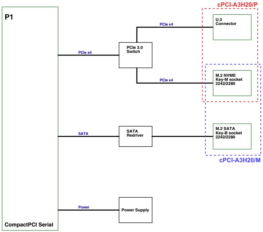
![This flowchart illustrates the signal routing for a 'P1' block labeled 'CompactPCI Serial' on the far left. It branches into three distinct paths:\n\n**Top Path (PCIe):**\n*   A connection labeled **'PCIe x4'** links **'P1'** to a **'PCIe 3.0 Switch'**.\n*   From the switch, two connections labeled **'PCIe x4'** branch out:\n    1.  One connects to a **'U.2 Connector'**. This block is enclosed in a red dashed box labeled **'cPCI-A3H20/P'**.\n    2.  The other connects to an **'M.2 NVME Key-M socket 2242/2280'**.\n\n**Middle Path (SATA):**\n*   A connection labeled **'SATA'** links **'P1'** to a **'SATA Redriver'**.\n*   From the redriver, a line connects to an **'M.2 SATA Key-B socket 2242/2280'**.\n\n**Bottom Path (Power):**\n*   A connection labeled **'Power'** links **'P1'** to a **'Power Supply'**.\n\n**Grouping:**\n*   The **'M.2 NVME Key-M socket 2242/2280'** and **'M.2 SATA Key-B socket 2242/2280'** are both enclosed within a blue dashed box labeled **'cPCI-A3H20/M'**.](.cpci-a3h20-50m-00105-1000-04-preliminary/16487dd8e765452ed43a7f2be72a4d7f75ab27941a8656f9c20bf6e63a240526.jpg)

Figure 2-1: cPCI-A3H20 Functional Block Diagram

# 2.3 I/O Connectivity Table

<table><tr><td rowspan="2">Function</td><td colspan="2">cPCI-A3H20/P</td><td colspan="2">cPCI-A3H20/M</td></tr><tr><td>Faceplate</td><td>Onboard</td><td>Faceplate</td><td>Onboard</td></tr><tr><td>U.2 PCIe</td><td>-</td><td>Yes</td><td>-</td><td>-</td></tr><tr><td>M.2 PCIe</td><td>-</td><td>Yes</td><td>-</td><td>Yes</td></tr><tr><td>M.2 SATA</td><td>-</td><td>-</td><td>-</td><td>Yes</td></tr><tr><td>Status LEDs</td><td>PowerU.2 NVMeM.2 NVMe</td><td>-</td><td>PowerM.2 SATAM.2 NVMe</td><td>-</td></tr></table>

Table 2-2: cPCI-A3H20 I/O Connectivity

# 3 Board Interfaces

# 3.1 cPCI-A3H20 Board Layout

![CN1\nCN2\nCN3\nP1](.cpci-a3h20-50m-00105-1000-04-preliminary/66e380b144751a25a4480e05d1c20b2182e157f5272cf65201522740d44df6dd.jpg)

<table><tr><td>P1</td><td>CompactPCI Serial P1 connectors</td></tr><tr><td>CN1</td><td>U.2 NVMe connector</td></tr><tr><td>CN2</td><td>M.2 B-Key 2280 SATA connector</td></tr><tr><td>CN3</td><td>M.2 M-Key 2280 NVMe connector (PCIe mode only)</td></tr></table>

Figure 3-1: cPCI-A3H20 Board Layout

# 3.2 cPCI-A3H20/P Assembly Layout

![U.2\nM.2\nM-Key](.cpci-a3h20-50m-00105-1000-04-preliminary/7313682611a0173eaa7b8b62a2b41bda5cac1a1c46c687aa48bf2af32f1067d5.jpg)

Figure 3-2: cPCI-A3H20/P Assembly Layout

# 3.3 cPCI-A3H20/M Assembly Layout

![M.2\nB-Key\nM.2\nM-Key](.cpci-a3h20-50m-00105-1000-04-preliminary/6e9438702f7c27c24de649851f2892208d7a8e5a7acd22afd2a9a62273c5c076.jpg)

Figure 3-3: cPCI-A3H20/M Assembly Layout

# 3.4 cPCI-A3H20 Front Panel

Front Panel Layout
![Power LED\nLED1 LED2 LED3](.cpci-a3h20-50m-00105-1000-04-preliminary/7370188d1931809d98537ad4c9db70466d6a6b2c86f98cbe69b65c56e378d969.jpg)

Figure 3-4: cPCI-A3H20 Front Panel Layout

Status LEDs

<table><tr><td>LED</td><td>Function</td><td>Condition</td><td>Indication</td></tr><tr><td rowspan="2">Power</td><td rowspan="2">Status</td><td>On</td><td>Power good</td></tr><tr><td>Off</td><td>No power</td></tr><tr><td rowspan="3">1 (cPCI-A3H20/P only)</td><td rowspan="3">U.2 NVMe</td><td>On</td><td>Power good</td></tr><tr><td>Blinking</td><td>Transmitting</td></tr><tr><td>Off</td><td>Not working</td></tr><tr><td rowspan="3">2</td><td rowspan="3">M.2 NVMe</td><td>On</td><td>Power good</td></tr><tr><td>Blinking</td><td>Transmitting</td></tr><tr><td>Off</td><td>Not working</td></tr><tr><td rowspan="3">3 (cPCI-A3H20/M only)</td><td rowspan="3">M.2 SATA</td><td>On</td><td>Power good</td></tr><tr><td>Blinking</td><td>Transmitting</td></tr><tr><td>Off</td><td>Not working</td></tr></table>

Table 3-1: cPCI-A3H20 Front Panel Status LED Descriptions

# 3.5 Connector Pin Assignments

# U.2 NVMe (CN1)

![E07\nE16\nS08\nS28\nE17\nE25\nP01\nP15\nS01\nS07\nE06\nE01](.cpci-a3h20-50m-00105-1000-04-preliminary/e70110e299a290240e3c86d375025d22d633dba25ce49aff8376407fbd9eee75.jpg)

<table><tr><td>Pin</td><td>Signal Name</td><td>Pin</td><td>Signal Name</td></tr><tr><td>S1</td><td>GND</td><td>E7</td><td>U2_PCIE_CLK0_P</td></tr><tr><td>S2</td><td>N/C</td><td>E8</td><td>U2_PCIE_CLK0_N</td></tr><tr><td>S3</td><td>N/C</td><td>E9</td><td>GND</td></tr><tr><td>S4</td><td>GND</td><td>E10</td><td>U2_PCIE_TX0_P</td></tr><tr><td>S5</td><td>N/C</td><td>E11</td><td>U2_PCIE_TX0_N</td></tr><tr><td>S6</td><td>N/C</td><td>E12</td><td>GND</td></tr><tr><td>S7</td><td>GND</td><td>E13</td><td>U2_PCIE_RX0_N</td></tr><tr><td>E1</td><td>N/C</td><td>E14</td><td>U2_PCIE_RX0_P</td></tr><tr><td>E2</td><td>N/C</td><td>E15</td><td>GND</td></tr><tr><td>E3</td><td>P_+3V3_A</td><td>E16</td><td>N/C</td></tr><tr><td>E4</td><td>N/C</td><td>S8</td><td>GND</td></tr><tr><td>E5</td><td>PLTRST_U2_KEY_N</td><td>S9</td><td>N/C</td></tr><tr><td>E6</td><td>N/C</td><td>S10</td><td>N/C</td></tr><tr><td>P1</td><td>U2_WAKE_N</td><td>S11</td><td>GND</td></tr><tr><td>P2</td><td>sPCIeRst</td><td>S12</td><td>N/C</td></tr><tr><td>P3</td><td>ClkReq#</td><td>S13</td><td>N/C</td></tr><tr><td>P4</td><td>FDET_N</td><td>S14</td><td>GND</td></tr><tr><td>P5</td><td>GND</td><td>S15</td><td>N/C</td></tr><tr><td>P6</td><td>GND</td><td>S16</td><td>GND</td></tr><tr><td>P7</td><td>N/C</td><td>S17</td><td>U2_PCIE_TX1_P</td></tr><tr><td>P8</td><td>N/C</td><td>S18</td><td>U2_PCIE_TX1_N</td></tr><tr><td>P9</td><td>N/C</td><td>S19</td><td>GND</td></tr><tr><td>P10</td><td>U2_PRSNT_N</td><td>S20</td><td>U2_PCIE_RX1_N</td></tr></table>

Table 3-2: U.2 NVMe Pin Definition

<table><tr><td>Pin</td><td>Signal Name</td><td>Pin</td><td>Signal Name</td></tr><tr><td>P11</td><td>LED_U2_ACT#</td><td>S21</td><td>U2_PCIE_RX1_P</td></tr><tr><td>P12</td><td>GND</td><td>S22</td><td>GND</td></tr><tr><td>P13</td><td>P_+12V_A</td><td>S23</td><td>U2_PCIE_TX2_P</td></tr></table>

Table 3-2: U.2 NVMe Pin Definition

M.2 Socket B-Key 2280 SATA (CN2)
![1\n75\nH](.cpci-a3h20-50m-00105-1000-04-preliminary/4f2601fe4da26ff3361ff4189199e9d9d009bdb5dca1341bdf44f957a114b4da.jpg)

<table><tr><td>Pin</td><td>Signal Name</td><td>Pin</td><td>Signal Name</td></tr><tr><td>1</td><td>GND</td><td>2</td><td>P_+3V3_A</td></tr><tr><td>3</td><td>GND</td><td>4</td><td>P_+3V3_A</td></tr><tr><td>5</td><td>GND</td><td>6</td><td>TP10</td></tr><tr><td>7</td><td>P1_USB2_P</td><td>8</td><td>TP11</td></tr><tr><td>9</td><td>P1_USB2_N</td><td>10</td><td>LED_M2_KEYB_ACT#</td></tr><tr><td>11</td><td>GND</td><td></td><td></td></tr><tr><td colspan="4">B-Key</td></tr><tr><td>21</td><td>GND</td><td>20</td><td>N/C</td></tr><tr><td>23</td><td>N/C</td><td>22</td><td>N/C</td></tr><tr><td>25</td><td>M2_1_DPR</td><td>24</td><td>N/C</td></tr><tr><td>27</td><td>GND</td><td>26</td><td>N/C</td></tr><tr><td>29</td><td>Reserved for USB</td><td>28</td><td>N/C</td></tr><tr><td>31</td><td>Reserved for USB</td><td>30</td><td>N/C</td></tr><tr><td>33</td><td>GND</td><td>32</td><td>N/C</td></tr><tr><td>35</td><td>Reserved for USB</td><td>34</td><td>N/C</td></tr><tr><td>37</td><td>Reserved for USB</td><td>36</td><td>N/C</td></tr><tr><td>39</td><td>GND</td><td>38</td><td>N/C</td></tr><tr><td>41</td><td>P1_SATA_M2_TX_P</td><td>40</td><td>N/C</td></tr><tr><td>43</td><td>P1_SATA_M2_TX_N</td><td>42</td><td>N/C</td></tr><tr><td>45</td><td>GND</td><td>44</td><td>N/C</td></tr><tr><td>47</td><td>P1_SATA_M2_RX_N</td><td>46</td><td>N/C</td></tr><tr><td>49</td><td>P1_SATA_M2_RX_P</td><td>48</td><td>N/C</td></tr><tr><td>51</td><td>GND</td><td>50</td><td>PLTRST_M2_KEY-B_N</td></tr><tr><td>53</td><td>N/C</td><td>52</td><td>M2_KEY-B_CLKREQ_N</td></tr><tr><td>55</td><td>N/C</td><td>54</td><td>M2_KEY-B_WAKE_N</td></tr><tr><td>57</td><td>GND</td><td>56</td><td>N/C</td></tr><tr><td>59</td><td>N/C</td><td>58</td><td>N/C</td></tr></table>

Table 3-3: M.2 B-Key 2280 SATA Pin Definition

<table><tr><td>Pin</td><td>Signal Name</td><td>Pin</td><td>Signal Name</td></tr><tr><td>61</td><td>N/C</td><td>60</td><td>N/C</td></tr><tr><td>63</td><td>N/C</td><td>62</td><td>N/C</td></tr><tr><td>65</td><td>N/C</td><td>64</td><td>N/C</td></tr><tr><td>67</td><td>PLTRST_M2_KEY-B_N</td><td>66</td><td>N/C</td></tr><tr><td>69</td><td>GND</td><td>68</td><td>N/C</td></tr><tr><td>71</td><td>GND</td><td>70</td><td>P_+3V3_A</td></tr><tr><td>73</td><td>GND</td><td>72</td><td>P_+3V3_A</td></tr><tr><td>75</td><td>GND</td><td>74</td><td>P_+3V3_A</td></tr></table>

Table 3-3: M.2 B-Key 2280 SATA Pin Definition

![The image displays a white document icon with a folded top-right corner and faint gray horizontal lines representing text. Superimposed over the document is a large, bold, red checkmark that runs diagonally from the bottom left to the upper right.](.cpci-a3h20-50m-00105-1000-04-preliminary/0efe36f243f043082703aadf76dedfc4a739ae40a17d04df1c51393741e2961c.jpg)
NOTE:

Pins 29, 31, 35 and 37 are reserved for USB. Please contact your ADLINK representative for more information.

M.2 Socket M-Key 2280 NVMe (CN3)
![1\n75\n2\n74](.cpci-a3h20-50m-00105-1000-04-preliminary/57f6774bb0f903a94237c5c617cea55e7a123b716ecd2129cebd76b23460762b.jpg)

<table><tr><td>Pin</td><td>Signal Name</td><td>Pin</td><td>Signal Name</td></tr><tr><td>1</td><td>GND</td><td>2</td><td>P_+3V3_A</td></tr><tr><td>3</td><td>GND</td><td>4</td><td>P_+3V3_A</td></tr><tr><td>5</td><td>M2_PCIE_RX3_P</td><td>6</td><td>N/C</td></tr><tr><td>7</td><td>M2_PCIE_RX3_N</td><td>8</td><td>N/C</td></tr><tr><td>9</td><td>GND</td><td>10</td><td>LED_M2_KEYM_ACT#</td></tr><tr><td>11</td><td>M2_PCIE_TX3_P</td><td>12</td><td>P_+3V3_A</td></tr><tr><td>13</td><td>M2_PCIE_TX3_N</td><td>14</td><td>P_+3V3_A</td></tr><tr><td>15</td><td>GND</td><td>16</td><td>P_+3V3_A</td></tr><tr><td>17</td><td>M2_PCIE_RX2_P</td><td>18</td><td>P_+3V3_A</td></tr><tr><td>19</td><td>M2_PCIE_RX2_N</td><td>20</td><td>N/C</td></tr><tr><td>21</td><td>GND</td><td>22</td><td>N/C</td></tr><tr><td>23</td><td>M2_PCIE_TX2_P</td><td>24</td><td>N/C</td></tr><tr><td>25</td><td>M2_PCIE_TX2_N</td><td>26</td><td>N/C</td></tr><tr><td>27</td><td>GND</td><td>28</td><td>N/C</td></tr><tr><td>29</td><td>M2_PCIE_RX1_P</td><td>30</td><td>N/C</td></tr><tr><td>31</td><td>M2_PCIE_RX1_N</td><td>32</td><td>N/C</td></tr><tr><td>33</td><td>GND</td><td>34</td><td>N/C</td></tr><tr><td>35</td><td>M2_PCIE_TX1_P</td><td>36</td><td>N/C</td></tr><tr><td>37</td><td>M2_PCIE_TX1_N</td><td>38</td><td>M2_1_DEVSLP</td></tr><tr><td>39</td><td>GND</td><td>40</td><td>N/C</td></tr><tr><td>41</td><td>M2_PCIE_RX0_P</td><td>42</td><td>N/C</td></tr><tr><td>43</td><td>M2_PCIE_RX0_N</td><td>44</td><td>N/C</td></tr><tr><td>45</td><td>GND</td><td>46</td><td>N/C</td></tr><tr><td>47</td><td>M2_PCIE_TX0_P</td><td>48</td><td>N/C</td></tr><tr><td>49</td><td>M2_PCIE_TX0_N</td><td>50</td><td>PLTRST_M2_KEY-M_N</td></tr><tr><td>51</td><td>GND</td><td>52</td><td>M2_KEY-M_CLK_REQ_N</td></tr></table>

Table 3-4: M.2 M-Key 2280 NVMe Pin Definition

<table><tr><td>Pin</td><td>Signal Name</td><td>Pin</td><td>Signal Name</td></tr><tr><td>53</td><td>M2_PCIE_CLK0_N</td><td>54</td><td>M2_KEY-M_PEWAKE_N</td></tr><tr><td>55</td><td>M2_PCIE_CLK0_P</td><td>56</td><td>N/C</td></tr><tr><td>57</td><td>GND</td><td>58</td><td>N/C</td></tr><tr><td colspan="4">M-Key</td></tr><tr><td>67</td><td>NC</td><td>68</td><td>M2_1_SUSCLK</td></tr><tr><td>69</td><td>P_+3V3_A</td><td>70</td><td>P_+3V3_A</td></tr><tr><td>71</td><td>GND</td><td>72</td><td>P_+3V3_A</td></tr><tr><td>73</td><td>GND</td><td>74</td><td>P_+3V3_A</td></tr><tr><td>75</td><td>GND</td><td></td><td></td></tr></table>

Table 3-4: M.2 M-Key 2280 NVMe Pin Definition

CompactPCI Serial P1 Connector

<table><tr><td>L</td><td>K</td><td>J</td><td>I</td><td>H</td><td>G</td><td>F</td><td>E</td><td>D</td><td>C</td><td>B</td><td>A</td><td></td></tr><tr><td>1_PE_RX03-</td><td>1_PE_RX03+</td><td>GND</td><td>1_PE_TX03-</td><td>1_PE_TX03+</td><td>GND</td><td>1_PE_RX02-</td><td>1_PE_RX02+</td><td>GND</td><td>1_PE_TX02-</td><td>1_PE_TX02+</td><td>GND</td><td>6</td></tr><tr><td>GND</td><td>1_PE_RX01-</td><td>1_PE_RX01+</td><td>GND</td><td>1_PE_TX01-</td><td>1_PE_TX01+</td><td>GND</td><td>1_PE_RX00-</td><td>1_PE_RX00+</td><td>GND</td><td>1_PE_TX00-</td><td>1_PE_TX00+</td><td>5</td></tr><tr><td>1_SATA_Rx-</td><td>1_SATA_RX+</td><td>GND</td><td>1_SATA_TX-</td><td>1_SATA_TX+</td><td>GND</td><td>PE_CL_KIN-</td><td>PE_CL_KIN+</td><td>GND</td><td>1_USB_2-</td><td>1_USB_2+</td><td>GND</td><td>4</td></tr><tr><td>GA3</td><td>SATA_SL</td><td>SATA_SCL</td><td>GA2</td><td>SATA_SDO</td><td>SATA_SDI</td><td>GA1</td><td>1_USB_3_RX-</td><td>1_USB_3_RX+</td><td>GA0</td><td>1_USB_3_TX-</td><td>1_USB_3_TX+</td><td>3</td></tr><tr><td>SYSEN#</td><td>PCIE_EN#</td><td>GND</td><td>WAKE_IN_OUT#</td><td>RST #</td><td>GND</td><td>Reser ved</td><td>Reser ved</td><td>GND</td><td>I2_C_SDA</td><td>I2C_SCL</td><td>GND</td><td>2</td></tr><tr><td>GND</td><td>+12V</td><td>+12V</td><td>GND</td><td>+12V</td><td>+12V</td><td>GND</td><td>+12V</td><td>+12V</td><td>GND</td><td>P5VSB</td><td>+12V</td><td>1</td></tr></table>

Table 3-5: CompactPCI Serial P1 Connector Pin Definition

![USB\nSATA\nPCIe\nPOWER\nGND\nSystem](.cpci-a3h20-50m-00105-1000-04-preliminary/1b6a24a3f91bbd55f15ac25f8a3600f46eb4700af68c4f4aa41e9feab32ddaab.jpg)

Figure 3-5: CompactPCI Serial P1 Pin Definition Legend

# 4 Getting Started

This chapter describes the following installation procedures for the cPCI-A3H20 carrier blade:

 2.5" U.2 NVMe drive (cPCI-A3H20/P only)
 M.2 M-Key NVMe module
 M.2 B-Key SATA module (cPCI-A3H20/M only)

# 4.1 cPCI-A3H20/P

# 2.5" U.2 NVMe Drive Installation

The cPCI-A3H20/P provides space to install a 2.5" U.2 NVMe drive. Install the drive to the bracket by inserting it into the U.2 connector and fastening the four screws provided as shown below.

![Technical line drawing of an electronic device chassis with exploded view (no text or symbols)](.cpci-a3h20-50m-00105-1000-04-preliminary/6881dc6b469deec65bcf1673a1b027529ef47fd6375d126da46aabf1dd13ccff.jpg)

# M.2 M-Key NVMe Module Installation

The cPCI-A3H20/P provides space to install an M.2 NVMe module. Install the module by inserting it into the M.2 connector and fastening the screw provided as shown below.

![Technical line drawing of an electronic device chassis with mounting brackets and connectors (no text or symbols)](.cpci-a3h20-50m-00105-1000-04-preliminary/1e918f669221901c9ff8bf334a13db7003fa1f86653df36a6f3270e0b25c5046.jpg)

# 4.2 cPCI-A3H20/M

# M.2 B-Key SATA and M-Key NVMe Module Installation

The cPCI-A3H20/M provides space to install an M.2 B-Key SATA and M.2 M-Key NVMe module. Install each module by inserting it into the corresponding M.2 connector and fastening the screw provided as shown below. Refer to “cPCI-A3H20 Board Layout” on page 7 for the locations of the M.2 B-Key SATA connector (CN2) and M.2 M-Key NVMe connector (CN3) locations.

![B-Key\nM-Key](.cpci-a3h20-50m-00105-1000-04-preliminary/3f9f342d482b7f7339b2852ac03a62ac5938049091fda836d9f24010c2ccdf11.jpg)

# 4.3 M.2 2242 Modules

To install M.2 2242 modules, remove the standoff from the default location (for M.2 2880 modules) and reinstall it in the location shown.

![CN2\nCN3](.cpci-a3h20-50m-00105-1000-04-preliminary/18860781643d9fe5162fe173c861f1168cd11297be1257f0625eea04920251fa.jpg)

This page intentionally left blank.

# Important Safety Instructions

For user safety, please read and follow all instructions, WARNINGS, CAUTIONS, and NOTES marked in this manual and on the associated equipment before handling/operating the equipment.

 Read these safety instructions carefully.
 Keep this user’s manual for future reference.
 Read the specifications section of this manual for detailed information on the operating environment of this equipment.
 When installing/mounting or uninstalling/removing equipment:
 Turn off power and unplug any power cords/cables.
 To avoid electrical shock and/or damage to equipment:
 Keep equipment away from water or liquid sources;
 Keep equipment away from high heat or high humidity;
 Keep equipment properly ventilated (do not block or cover ventilation openings);
 Make sure to use recommended voltage and power source settings;
 Always install and operate equipment near an easily accessible electrical socket-outlet;
 Secure the power cord (do not place any object on/over the power cord);
 Only install/attach and operate equipment on stable surfaces and/or recommended mountings; and,
 If the equipment will not be used for long periods of time, turn off and unplug the equipment from its power source.

 Never attempt to fix the equipment. Equipment should only be serviced by qualified personnel.

A Lithium-type battery may be provided for uninterrupted, backup or emergency power.

![The image displays a red triangle with a white exclamation point centered inside. Below the triangle, the word 'WARNING' is printed in black capital letters on a white background.](.cpci-a3h20-50m-00105-1000-04-preliminary/090c6c4395f837b8069fcff02b6e5a4b169f9cef8738ae9a675b545fb96d7d43.jpg)

Risk of explosion if battery is replaced with one of an incorrect type. Dispose of used batteries appropriately.

 Equipment must be serviced by authorized technicians when:

 The power cord or plug is damaged;
 Liquid has penetrated the equipment;
 It has been exposed to high humidity/moisture;
 It is not functioning or does not function according to the user’s manual;
 It has been dropped and/or damaged; and/or,
 It has an obvious sign of breakage.

# Getting Service

Ask an Expert: http://askanexpert.adlinktech.com

# ADLINK Technology, Inc.

No. 66, Huaya 1st Rd., Guishan District

Taoyuan City 333411, Taiwan

Tel: +886-3-216-5088

Fax: +886-3-328-5706

Email: service@adlinktech.com

# Ampro ADLINK Technology, Inc.

6450 Via Del Oro

San Jose, CA 95119-1208, USA

Tel: +1-408-360-0200

Toll Free: +1-800-966-5200 (USA only)

Fax: +1-408-600-1189

Email: info@adlinktech.com

# ADLINK Technology (China) Co., Ltd.

300 Fang Chun Rd., Zhangjiang Hi-Tech Park

Pudong New Area, Shanghai, 201203 China

Tel: +86-21-5132-8988

Fax: +86-21-5132-3588

Email: market@adlinktech.com

# ADLINK Technology GmbH

Hans-Thoma-Strasse 11

D-68163 Mannheim, Germany

Tel: +49-621-43214-0

Fax: +49-621 43214-30

Email: emea@adlinktech.com

Please visit the Contact page at www.adlinktech.com for information on how to contact the ADLINK regional office nearest you.
[🔗 Link to the original document](.cpci-a3h20-50m-00105-1000-04-preliminary/cpci-a3h20-50m-00105-1000-04-preliminary.pdf)
