# DLAP-201 Series

# DLAP-201-JT2 / DLAP-201-JT2i

# Edge Inference System

# User's Manual

![Black ADLINK industrial device with heat sinks and ports (no visible text or symbols on main body)](.dlap-201-jt2-50-1z308-1020-12/2b29159fc48f636a1cd255af1f7eb86c98194d15ba0820b02d9e2e4b65f4edea.jpg)

Manual Rev.: 1.2

Revision Date: August 19, 2020

Part No: 50-1Z308-1020

Revision History

<table><tr><td>Revision</td><td>Release Date</td><td>Description of Change(s)</td></tr><tr><td>1.0</td><td>2020-01-14</td><td>Initial Release</td></tr><tr><td>1.1</td><td>2020-05-26</td><td>Update specifications, COM port configuration; remove Wi-Fi function</td></tr><tr><td>1.2</td><td>2020-08-19</td><td>Update power adapter spec., system recovery host PC requirements; correct mSATA and Mini PCIe slot locations</td></tr></table>

# Preface

Copyright © 2020 ADLINK Technology, Inc.

This document contains proprietary information protected by copyright. All rights are reserved. No part of this manual may be reproduced by any mechanical, electronic, or other means in any form without prior written permission of the manufacturer.

# Disclaimer

The information in this document is subject to change without prior notice in order to improve reliability, design, and function and does not represent a commitment on the part of the manufacturer.

In no event will the manufacturer be liable for direct, indirect, special, incidental, or consequential damages arising out of the use or inability to use the product or documentation, even if advised of the possibility of such damages.

# Environmental Responsibility

ADLINK is committed to fulfill its social responsibility to global environmental preservation through compliance with the European Union's Restriction of Hazardous Substances (RoHS) directive and Waste Electrical and Electronic Equipment (WEEE) directive. Environmental protection is a top priority for ADLINK. We have enforced measures to ensure that our products, manufacturing processes, components, and raw materials have as little impact on the environment as possible. When products are at their end of life, our customers are encouraged to dispose of them in accordance with the product disposal and/or recovery programs prescribed by their nation or company.

# Trademarks

Product names mentioned herein are used for identification purposes only and may be trademarks and/or registered trademarks of their respective companies.

# Conventions

Take note of the following conventions used throughout this manual to make sure that users perform certain tasks and instructions properly.

![The image displays an icon of a white document with a folded top-right corner and horizontal blue lines running across the lower portion. A large, bold red checkmark is superimposed over the center of the document.](.dlap-201-jt2-50-1z308-1020-12/7eb8fc9cdf332f1b58f6b88db828f99f0ee1b56c3743c929f46b1f7bb8573a10.jpg)
NOTE:

Additional information, aids, and tips that help users perform tasks.

![A yellow triangular warning sign with a thick black border containing a large black exclamation point in the center.](.dlap-201-jt2-50-1z308-1020-12/981cb3522a2f86db7c68a5190ad3c14b98387edb3c559e66d4be4dc4e2d85ec2.jpg)
CAUTION:

Information to prevent minor physical injury, component damage, data loss, and/or program corruption when trying to complete a task.

Informations destinées à prévenir les blessures corporelles mineures, les dommages aux composants, la perte de données et/ou la corruption de programme lors de l'exécution d'une tâche.

![The image displays a red triangular warning sign with a white border. Inside the triangle, centered, is a white exclamation point.](.dlap-201-jt2-50-1z308-1020-12/9d85049fc7ee56db9badc72faf8e2ff3a73e613f3ce180a2651370299bd7a47f.jpg)
WARNING:

Information to prevent serious physical injury, component damage, data loss, and/or program corruption when trying to complete a specific task.

Informations destinées à prévenir les blessures corporelles graves, les dommages aux composants, la perte de données et/ou la corruption de programme lors de l'exécution d'une tâche spécifique.

# Table of Contents

# Preface...... iii

# List of Tables...... vii

# List of Figures ix

# 1 Introduction ...... 1

1.1 Features.... 1
1.2 Specifications.... 2
1.3 Mechanical Dimensions.... 4
1.4 External Layout.... 5
1.5 Pin Definitions.... 7

1.5.1 Ethernet GbE Connectors 7
1.5.2 USB 3.0 Connectors....8
1.5.3 12 Volt DC Connector....9
1.5.4 CAN Bus.... 10
1.5.5 COM Port (Serial Port) 10
1.5.6 HDMI Connectors 11
1.5.7 USB 2.0 OTG Connector....11
1.5.8 Side I/O Slots.... 12

# 2 Getting Started 15

2.1 Unpacking Checklist 15
2.2 Cooling Considerations.... 15
2.3 Removing the Chassis Cover 16
2.4 Installing an mSATA Module 18
2.5 Installing a Mini PCIe 3G/4G LTE Module 19
2.6 Connecting DC Power 20
2.7 VESA Mount 21
2.8 DIN Rail Mount 22
2.9 Internal Jumper Settings.... 23

2.9.1 COM Mode Switches....24
2.9.2 AT Mode Switch (SWS1501) 24
2.9.3 GPIO Switch (CN1501)....24

# 3 Using the System.... 25

3.1 Software Configuration 25
3.2 System Recovery.... 25
3.3 COM Port Configuration.... 27

# Important Safety Instructions.... 29

# Getting Service 31

# List of Tables

Table 1-1: Specifications .... 3

Table 1-2: Front Panel I/O Connectors & Controls .... 5

Table 1-3: Rear Panel I/O Connectors 6

Table 1-4: RJ-45 GbE Pin Definition....7

Table 1-5: USB 3.0 Pin Definition 8

Table 1-6: 12 Volt DC Connector Pin Definition 9

Table 1-7: CAN Bus Pin Definition....10

Table 1-8: RS-232/422/485 Connector Pin Definition.... 10

Table 1-9: HDMI Connector Pin Definition.... 11

Table 1-10: USB 2.0 OTG Connector Pin Information.... 11

Table 2-1: COM Mode Switches....24

Table 2-2: AT Mode Switch 24

Table 2-3: GPIO Switch 24

This page intentionally left blank.

# List of Figures

Figure 1-1: Front View Dimensions....4

Figure 1-2: Side View Dimensions....4

Figure 1-3: Front Panel I/O Connectors & Controls .... 5

Figure 1-4: Rear Panel I/O Connectors 6

Figure 1-5: 12 Volt DC Connector Mechanical Specification ..... 9

Figure 1-6: USIM / SD Side Door....12

Figure 2-1: mSATA Slot....18

Figure 2-2: Mini PCIe 3G/4G LTE Slot....19

Figure 2-3: VESA Mount 21

Figure 2-4: DIN Rail Mount 22

Figure 2-5: Internal Jumpers....23

Figure 3-1: Successful USB 2.0 Connection....26

This page intentionally left blank.

# 1 Introduction

ADLINK's DLAP-201 Series Edge Inference System leverages the power of NVIDIA® Jetson™ TX2/TX2i modules to deliver artificial intelligence (AI) at the edge. The DLAP-201-JT2 Edge AI Platform with integrated NVIDIA Jetson TX2 accelerates deep learning workloads for object detection, recognition, and classification. With the rapidly increased adoption of AI across industries, the DLAP-201-JT2 can be useful for a wide variety of smart city and smart manufacturing applications, including real-time traffic flow analysis at an intersection for traffic management optimization, improvement of smart bus services, strengthening of security surveillance, and many others.

The DLAP-201 Series provides a wide variety of industrial I/O and visual inferencing capabilities in a compact system. With a lockable HDMI display, two GbE ports, three USB 3.0 ports (plus a USB 2.0 OTG port for software updates), one COM port, one isolated CAN bus, one audio jack (headphone), 32GB of eMMC storage plus one mSATA and one SD slot for additional storage options, and a Mini PCIe slot and USIM socket to support other wireless communications such as LoRa and 3G/4G LTE, the DLAP-201-JT2 enables AI at the edge with exceptional performance and convenience while keeping power consumption to a minimum.

# 1.1 Features

▶ Deep learning acceleration with NVIDIA® Jetson™ TX2/TX2i
▶ NVIDIA® Pascal™ GPU with 256 CUDA cores
▶ 8GB 128-bit LPDDR4
▶ 32GB eMMC plus SDIO and mSATA storage interfaces
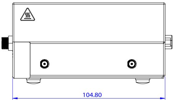
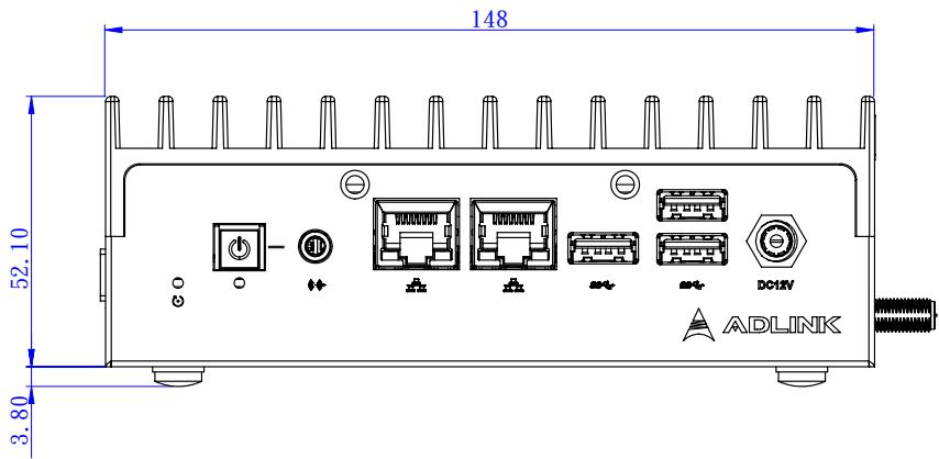
▶ Compact fanless system: 148(W) x 104.8(D) x 52.1(H) mm
▶ Wide temperature range: $-20^{\circ}C$ to $70^{\circ}C$

# 1.2 Specifications

<table><tr><td>Item</td><td>Description</td></tr><tr><td colspan="2">System Core</td></tr><tr><td>Processor</td><td>NVIDIA Jetson TX2 (TX2i optional)</td></tr><tr><td>Memory</td><td>8GB 128-bit LPDDR4</td></tr><tr><td>Storage</td><td>32GB eMMC 5.1</td></tr><tr><td colspan="2">Graphic Output</td></tr><tr><td>Graphic Output</td><td>1x HDMI 2.0 with lock (3840x2160 @60fps)</td></tr><tr><td colspan="2">Front Panel I/O Interface</td></tr><tr><td>Ethernet</td><td>2x GbE</td></tr><tr><td>USB 3.0</td><td>3x Type-A</td></tr><tr><td>Audio</td><td>1x audio jack (headphone)</td></tr><tr><td colspan="2">Rear Panel I/O Interface</td></tr><tr><td>USB</td><td>1x USB 2.0 OTG (Micro-USB)</td></tr><tr><td>Serial Port</td><td>1x COM port (DE-9 connector)</td></tr><tr><td>CAN Bus</td><td>1x CAN bus (2.0B)</td></tr><tr><td colspan="2">Internal I/O Interface</td></tr><tr><td>Mini PCIe</td><td>1x Mini PCIe slot (linked to USIM)</td></tr><tr><td>USIM</td><td>1x USIM slot (standard size)</td></tr><tr><td>DIO</td><td>4 channel DIO</td></tr><tr><td>Debug Port</td><td>1x debug console</td></tr><tr><td colspan="2">Storage Devices</td></tr><tr><td>SATA</td><td>mSATA (full size)</td></tr><tr><td>SD Card</td><td>1x SDIO</td></tr><tr><td colspan="2">Power</td></tr><tr><td>DC Input</td><td>12V</td></tr><tr><td>AC Input</td><td>Optional 60W AC-DC adapter (ADLINK P/N: 31-62156-1000-A0)</td></tr><tr><td>Fail Reset</td><td>Reset and recovery buttons</td></tr><tr><td>Buttons</td><td>Power button w/ LED indicator</td></tr><tr><td colspan="2">CMOS Battery</td></tr><tr><td>Type</td><td>BR2032</td></tr><tr><td>Protection</td><td>Reverse charge protection</td></tr></table>

<table><tr><td>Item</td><td>Description</td></tr><tr><td colspan="2">Mechanical</td></tr><tr><td>Antenna Holes</td><td>4x SMA</td></tr><tr><td>Dimensions</td><td>148(W) x 104.8(D) x 52.1(H) mm</td></tr><tr><td>Weight</td><td>765g</td></tr><tr><td>Mounting</td><td>VESA (DIN rail optional)</td></tr><tr><td colspan="2">Environmental</td></tr><tr><td>Operating Temperature</td><td>Standard -20°C to 70°C</td></tr><tr><td>Operating Humidity</td><td>95% @40°C (non-condensing)</td></tr><tr><td>Storage Temperature</td><td>-40°C to 85°C</td></tr><tr><td>Vibration</td><td>Operating: 5Grms, 5 to 500 Hz, 3 axes w/ mSATA</td></tr><tr><td>Shock</td><td>Operating: 100G, half sine 11 ms duration w/ SD, mSATA</td></tr><tr><td>ESD</td><td>Contact +/- 4kV, Air +/- 8kV</td></tr><tr><td>EMC</td><td>CE &amp; FCC class B, (EN61000-6-4/-6-2)</td></tr><tr><td>Safety</td><td>IEC/CE/UL standard</td></tr><tr><td>RF Regulations</td><td>FCCID</td></tr><tr><td colspan="2">Operating System Support</td></tr><tr><td>Linux</td><td>Linux for Tegra (L4T)</td></tr></table>

Table 1-1: Specifications

# 1.3 Mechanical Dimensions

All dimensions shown in millimeters (mm).
![148\n52.10\n3.80\nADLINK](.dlap-201-jt2-50-1z308-1020-12/551b4e238102d3f3c6abe6dd401d245c6c08704dc27be9368c3f9a9833682bd4.jpg)

Figure 1-1: Front View Dimensions

![104.80](.dlap-201-jt2-50-1z308-1020-12/eee89ae7e6d47ee658cce3b50b0f1a3ce760c458674b96866490d834c8fdc749.jpg)

Figure 1-2: Side View Dimensions

# 1.4 External Layout

Front Panel
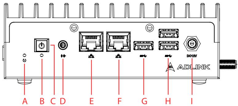
![A B C D E F G H I\nADLINK](.dlap-201-jt2-50-1z308-1020-12/0e8bab97b3441ab09871df43a082a58c5eca0a65e0a0c9fb5054849cd4b1eb40.jpg)

Figure 1-3: Front Panel I/O Connectors & Controls

<table><tr><td>Item</td><td>Name</td><td>Description</td></tr><tr><td>A</td><td>Reset button</td><td>The reset button executes a hard reset on the system.</td></tr><tr><td>B</td><td>Recovery button</td><td>Press this button to force the system into recovery mode. See Section 3.2 System Recovery.</td></tr><tr><td>C</td><td>Power button</td><td>The power button is a non-latched push button with a blue LED power indicator. If the system is powered off when the button is pressed, the system powers up and the blue LED lights up. If the system hangs, pressing and holding the button continuously for 5 seconds performs a hard shutdown on the system.</td></tr><tr><td>D</td><td>Audio connector</td><td>One audio jack (headphone).</td></tr><tr><td>E</td><td>GbE connector (LAN 1)</td><td>GbE from NVIDIA® JetsonTM TX2. See Section 1.5 Pin Definitions.</td></tr><tr><td>F</td><td>GbE connector (LAN 2)</td><td>GbE from Intel® I210. See Section 1.5 Pin Definitions.</td></tr><tr><td>G - H</td><td>USB 3.0 x 3</td><td>See Section 1.5.2 USB 3.0 Connectors.</td></tr><tr><td>I</td><td>DC connector 12V</td><td>12V DC screw-type connector. See Section 1.5.3 12 Volt DC Connector.</td></tr></table>

Table 1-2: Front Panel I/O Connectors & Controls

Rear Panel
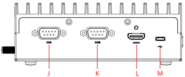
![CAN\nCOM\nHAN\nJ\nK\nL\nM](.dlap-201-jt2-50-1z308-1020-12/3f16c32799969c85be8a76ca1e8fe437d5da9333bcd338bff2ba2a765742286b.jpg)

Figure 1-4: Rear Panel I/O Connectors

<table><tr><td>Item</td><td>Name</td><td>Description</td></tr><tr><td>J</td><td>CAN bus</td><td>CAN 2.0B (backward compatible with 2.0A)</td></tr><tr><td>K</td><td>Serial port</td><td>COM port (DE-9 connector); RS-232/422/485 supported by jumper selection</td></tr><tr><td>L</td><td>HDMI port</td><td>HDMI 2.0 with lock</td></tr><tr><td>M</td><td>USB 2.0</td><td>USB 2.0 OTG (Micro-USB)</td></tr></table>

Table 1-3: Rear Panel I/O Connectors

# 1.5 Pin Definitions

# 1.5.1 Ethernet GbE Connectors

The DLAP-201 series comes with two RJ-45 connectors:

▶ NVIDIA® Jetson™ TX2 (LAN 1)
Intel® I210 (LAN 2)

LAN LED connection speed color indicators:

▶ Yellow (left LED): 1Gbps
▶ Green (right LED): 100Mbps

The following table provides details for the RJ-45 GbE pin connections.

<table><tr><td>Pin #</td><td>10BASE-T/100BASE-TX</td><td>1000BASE-T</td></tr><tr><td>1</td><td>TX+</td><td>LAN_TX0+</td></tr><tr><td>2</td><td>TX-</td><td>LAN_TX0-</td></tr><tr><td>3</td><td>RX+</td><td>LAN_TX1+</td></tr><tr><td>4</td><td>—</td><td>LAN_TX2+</td></tr><tr><td>5</td><td>—</td><td>LAN_TX2-</td></tr><tr><td>6</td><td>RX-</td><td>LAN_TX1-</td></tr><tr><td>7</td><td>—</td><td>LAN_TX3+</td></tr><tr><td>8</td><td>—</td><td>LAN_TX3-</td></tr></table>

Table 1-4: RJ-45 GbE Pin Definition

# 1.5.2 USB 3.0 Connectors

The USB 3.0 ports support a USB Type-A connection, compatible with SuperSpeed, Hi-Speed, full-speed, and low-speed USB devices. It is suitable for USB peripherals including USB cameras.

The following table provides details for the USB pin connections.

<table><tr><td>Pin #</td><td>Signal Name</td></tr><tr><td>1</td><td>USB3.0_P5VA</td></tr><tr><td>2</td><td>USB2_CMAN</td></tr><tr><td>3</td><td>USB2_CMAP</td></tr><tr><td>4</td><td>GND</td></tr><tr><td>5</td><td>USB3A_CMRXN</td></tr><tr><td>6</td><td>USB3A_CMRXP</td></tr><tr><td>7</td><td>GND</td></tr><tr><td>8</td><td>USB3A_CMTXN</td></tr><tr><td>9</td><td>USB3A_CMTXP</td></tr></table>

![1\n2\n3\n4\n5\n6\n7\n8\n9](.dlap-201-jt2-50-1z308-1020-12/d43101f9793646f31af0f2ca5f88790d6ea1b0417dea922388896d2e3f42d105.jpg)

Table 1-5: USB 3.0 Pin Definition

# 1.5.3 12 Volt DC Connector

The system requires a DC power source with a screw-type connector.

<table><tr><td>Pin</td><td>Signal</td></tr><tr><td>1</td><td>+12V</td></tr><tr><td>2</td><td>GND</td></tr><tr><td>3</td><td>GND</td></tr></table>

Table 1-6: 12 Volt DC Connector Pin Definition

![12.5±0.3\n3.0\n+0.1\nø5.6-0\n+0.2\n2.6-0\n+0.2\n0.25t\nDimensions: mm](.dlap-201-jt2-50-1z308-1020-12/c594976a3ad20d32aa413998763d11122205ca69bfcf1a2f9d2811f749ccfeee.jpg)

Figure 1-5: 12 Volt DC Connector Mechanical Specification

# 1.5.4 CAN Bus

The Controller Area Network (CAN) enables communication among devices. The table below provides CAN bus pin information.

<table><tr><td>Pin</td><td>Signal</td><td>Description</td></tr><tr><td>1</td><td>NC</td><td>(Not connected)</td></tr><tr><td>2</td><td>CAN0_Low</td><td>Differential CAN signal negative level</td></tr><tr><td>3</td><td>CAN0_GND</td><td>CAN interface ground</td></tr><tr><td>4</td><td>NC</td><td>(Not connected)</td></tr><tr><td>5</td><td>NC</td><td>(Not connected)</td></tr><tr><td>6</td><td>NC</td><td>(Not connected)</td></tr><tr><td>7</td><td>CAN0_High</td><td>Differential CAN signal positive level</td></tr><tr><td>8</td><td>NC</td><td>(Not connected)</td></tr><tr><td>9</td><td>NC</td><td>(Not connected)</td></tr></table>

![6\n1\n5](.dlap-201-jt2-50-1z308-1020-12/1e88e2de804e1fa369edfe452f2a1f4995fac26294135558dc0bb66690d27c6c.jpg)

Table 1-7: CAN Bus Pin Definition

# 1.5.5 COM Port (Serial Port)

RS-232/422/485 are supported by jumper selection. For details, see Section 2.9.1 COM Mode Switches on page 24.

<table><tr><td>Pin</td><td>RS-232</td><td>RS-422</td><td>RS-485</td></tr><tr><td>1</td><td>NC (not connected)</td><td>COM_TXD_N</td><td>COM_D-</td></tr><tr><td>2</td><td>COM_RXD</td><td>COM_TXD_P</td><td>COM_D+</td></tr><tr><td>3</td><td>COM_TXD</td><td>COM_RXD_P</td><td>NC</td></tr><tr><td>4</td><td>NC</td><td>COM_RXD_N</td><td>NC</td></tr><tr><td>5</td><td>COM_GND</td><td>NC</td><td>NC</td></tr><tr><td>6</td><td>NC</td><td>NC</td><td>NC</td></tr><tr><td>7</td><td>COM_RTS#</td><td>NC</td><td>NC</td></tr><tr><td>8</td><td>COM_RCTS#</td><td>NC</td><td>NC</td></tr><tr><td>9</td><td>NC</td><td>NC</td><td>NC</td></tr></table>

Table 1-8: RS-232/422/485 Connector Pin Definition

# 1.5.6 HDMI Connectors

The rear panel supports HDMI 2.0.

![19 17\n3 1\n18\n4 2](.dlap-201-jt2-50-1z308-1020-12/ce6c7840ec4512d36fd41eb8562a3c348cf4758421c04df6107b204497f0db6d.jpg)

<table><tr><td>Pin #</td><td>Signal</td><td>Pin #</td><td>Signal</td></tr><tr><td>1</td><td>TMDS Data2+</td><td>2</td><td>TMDS Data2 Shield</td></tr><tr><td>3</td><td>TMDS Data2-</td><td>4</td><td>TMDS Data1+</td></tr><tr><td>5</td><td>TMDS Data1 Shield</td><td>6</td><td>TMDS Data1-</td></tr><tr><td>7</td><td>TMDS Data0+</td><td>8</td><td>TMDS Data0 Shield</td></tr><tr><td>9</td><td>TMDS Data0-</td><td>10</td><td>TMDS Clock+</td></tr><tr><td>11</td><td>TMDS Clock Shield</td><td>12</td><td>TMDS Clock-</td></tr><tr><td>13</td><td>CEC</td><td>14</td><td>Reserved</td></tr><tr><td>15</td><td>SCL</td><td>16</td><td>SDA</td></tr><tr><td>17</td><td>DDC/CEC Ground</td><td>18</td><td>+5 V Power</td></tr><tr><td>19</td><td>Hot Plug Detect</td><td></td><td></td></tr></table>

Table 1-9: HDMI Connector Pin Definition

# 1.5.7 USB 2.0 OTG Connector

The DLAP-201 supports a USB 2.0 OTG Micro-USB Type-B connection for system recovery. The pin definition is as follows.

<table><tr><td>Pin</td><td>Signal</td><td>Description</td></tr><tr><td>1</td><td>VCC_USBDev</td><td>USB device power</td></tr><tr><td>2</td><td>USB_D1_n</td><td rowspan="2">Universal Serial Bus Port 1 / USB-Client differential pair</td></tr><tr><td>3</td><td>USB_D1_p</td></tr><tr><td>4</td><td>USB_ID</td><td>USB ID pin</td></tr><tr><td>5</td><td>GND_USBDev</td><td>USB GND</td></tr></table>

Table 1-10: USB 2.0 OTG Connector Pin Information

# 1.5.8 Side I/O Slots

The I/O connectors accessible from the right side panel of the DLAP-201 are described below.

![Technical line drawing of a device casing with labeled ports and internal components (no readable text or symbols)](.dlap-201-jt2-50-1z308-1020-12/49cbdbcfc3137d91c96c43a14e6ea70bef19ddb09cba88142162492374ecd105.jpg)

Figure 1-6: USIM / SD Side Door

# SD Card Slot

For additional storage, use the side door to install or remove a user-provided SD card.

# USIM Slot

The DLAP-201 is equipped with a USIM slot connected to the Mini PCIe connector for use with a user-provided SIM card and 3G/4G Mini PCIe module to provide cellular communication. Install or remove a SIM card module via the side door.

![The image displays a graphic of a white document or piece of paper with the top-right corner folded over (a 'dog-ear'). Faint grey horizontal lines run across the bottom half of the page, suggesting text. Superimposed over the document is a large, bold red checkmark (or tick) that extends diagonally from the bottom left to the top right.](.dlap-201-jt2-50-1z308-1020-12/d2360af70a16bc0129cb6d67145328e048353ecbdcea2650eb9cb10c82252570.jpg)
NOTE:

The 3G/4G Mini PCIe module requires a user-provided SIM card for communication via a telecom operator. See Section 2.5 Installing a Mini PCIe 3G/4G LTE Module on page 19.

# Orientation

Insert the SIM and SD cards with the orientations shown below.

![Close-up of a microSD adapter with a transparent flash module and a circuit board, placed on a green surface (no visible text or symbols)](.dlap-201-jt2-50-1z308-1020-12/f6109cac02e1847e76dd6c1bad5fecb7bcb928c32d02031d4dd1df8565387b0a.jpg)

This page intentionally left blank.

# 2 Getting Started

# 2.1 Unpacking Checklist

Before unpacking, check the shipping carton for any damage. If the shipping carton and/or contents are damaged, inform your dealer immediately. Retain the shipping carton and packing materials for inspection. Obtain authorization from your dealer before returning any product to ADLINK. Ensure that the following items are included in the package.

▶ DLAP-201 unit
▶ Screw pack
▶ VESA mount kit (plus optional DIN rail kit if applicable)

# 2.2 Cooling Considerations

All heat-generating components of the DLAP-201 are located on the left side of the system. These components directly contact the heat sink via thermal pads to dissipate heat. To maximize efficiency of heat dissipation, maintain a minimum of 2 inches (5cm) clearance on the top of the DLAP-201.

# 2.3 Removing the Chassis Cover

To access the DLAP-201's internals, remove the underside of the chassis as follows.

1. On the front panel, remove the nut and washer from the DC12V connector and remove the two mounting screws, all indicated by red circles in the figure below.

![Front view of a ADLINK network device showing ports, connectors, and ventilation slots (no readable text or symbols beyond branding)](.dlap-201-jt2-50-1z308-1020-12/50274510fed42646c617b002e35d6e28350d5a49f601eb81c680553e82890ece.jpg)

2. On the underside of the device, remove the screw indicated by the red circle.

![Close-up of a black electronic device with four pins and a red circle highlighting a positive button, set against a green background (no text or symbols)](.dlap-201-jt2-50-1z308-1020-12/b82c930c2ccddbb7babb8a72d841fd7394e265610c4fd55ef6f9a27dbf0b9fcc.jpg)

3. Slide the cover in the direction indicated by the red arrow to the position shown below.

![Close-up of a black rectangular electronic component with bolt holes and a red arrow pointing downward (no text or symbols)](.dlap-201-jt2-50-1z308-1020-12/1fcd1a1c3106878f59b7fd1e14d4375396c4949b5cfdecc2c9a20741adba68d2.jpg)

4. Lift the cover off of the chassis.

![Interior view of an electronic device with visible circuit board, capacitors, and connectors (no readable text or symbols)](.dlap-201-jt2-50-1z308-1020-12/713c9d28bcd7974ea84e9428a63306fcb5d89b143fb66b106d0808f6c5a943d4.jpg)

Reverse the steps above to replace the bottom cover.

# 2.4 Installing an mSATA Module

Use the following steps to install an mSATA module.

1. Insert the mSATA module into the indicated slot (under the wires) at an angle.

![ADLINK\nDAI-201-CB\n51-77B00.0\n5/N\n68T1B\n68T1B](.dlap-201-jt2-50-1z308-1020-12/eaa22a50f349f3ceedd64e9cf6aaa96e8545f1d1434198fd9a0f4d377da6b2cc.jpg)

Figure 2-1: mSATA Slot

2. Press down on the mSATA module until it is seated, then secure it with two M2.5-P-head-L5 screws (not provided).
3. Replace the bottom cover of the chassis.

![The image displays a yellow triangular warning sign with a black border, featuring a large black exclamation mark in the center.](.dlap-201-jt2-50-1z308-1020-12/a7b8b168ade4c68ba186ada5a8d9f45c716f462059c9d6a075451252a4bd619a.jpg)
CAUTION:

Take care not to remove or damage any wires while installing the module.

# 2.5 Installing a Mini PCIe 3G/4G LTE Module

Use the following steps to install a Mini PCIe 3G/4G LTE module.

![The image displays a white document icon with a black outline and a folded top-right corner. Faint horizontal lines run across the page. A large, bold red checkmark is superimposed over the document, running diagonally from the bottom left to the top right.](.dlap-201-jt2-50-1z308-1020-12/1e3eb2c9a9410e955a8b62ae911c0399a7adeb046142a423379834257bfbab33.jpg)
NOTE:

Use of the Mini PCIe 3G/4G LTE module requires installation of a SIM card. See Section 1.5.8 Side I/O Slots on page 12.

1. Insert the Mini PCIe 3G/4G LTE module into the indicated slot at an angle.

![ADLINK\nDIA-201-CB\n51-77800-0A20\n8BT10\n8BT13](.dlap-201-jt2-50-1z308-1020-12/e0d29c3d84dfaba709901a6c65dc2d05c3731fffcefcc0650feef74e5ad57170.jpg)

Figure 2-2: Mini PCIe 3G/4G LTE Slot

2. Press down on the module until it is seated, then secure it to the board using two M2.5-P-head-L5 screws (not provided).
3. Attach the wires and antennas that came with your 3G/4G LTE kit.
4. Replace the bottom cover of the chassis.

# 2.6 Connecting DC Power

![The image shows a standard safety warning sign. It features a red triangle with a white exclamation point in the center. Below the triangle is a white rectangular area containing the text 'WARNING:' in black, uppercase letters.](.dlap-201-jt2-50-1z308-1020-12/bf5d418d21c2884c9f5278d2ee91c4de940426fd376e2d42003f209970ababdc.jpg)

Before providing DC power to the DLAP-201, ensure the voltage and polarity provided are compatible with the DC input. Improper input voltage and/or polarity can be responsible for system damage.

Avant de connecter le PC DLAP-201 à une source de courant continu, veuillez vous assurer de la polarité de la tension conformément à l'entrée CC du PC. Une tension et/ou une polarité incorrectes peuvent causer des dommages irréversibles sur le système.

DC power sources must comply with LPS and SELV circuits with no energy hazard, as well as the following:

▶ IEC 62368-1 + IEC 60950-1 + UL 62368-1
▶ Output voltage: 12 VDC
▶ Output current: 2.7A minimum
▶ TMA: 50°C minimum

The DLAP-201 DC power input connector uses V+, V-, and chassis ground pins and accepts input voltage as shown previously.

Customers may optionally order a DC power adapter from ADLINK: DC plug with lock (part no. 31-62156-1000-A0).

# 2.7 VESA Mount

The DLAP-201 controller ships with a VESA 100 mounting bracket and four M4 screws. Follow the steps below to mount the device.

1. Attach the VESA bracket to the wall (or other suitable mounting surface) such that its keyhole-shaped mounting holes are oriented with the wider openings at the top.
2. Secure the four M4 screws to the bottom of the chassis.
3. Securely attach the device to the VESA bracket by first inserting the heads of the screws into the wider openings of the VESA bracket's mounting holes, then sliding the device down such that the screws are now firmly held by the narrower portions of the mounting holes.

![Technical line drawing of an electronic device chassis with mounting brackets and ports (no text or symbols)](.dlap-201-jt2-50-1z308-1020-12/d749a08c3150164873acc72f3387d378be721cb6e8ea8cf39a104c2090fccfcd.jpg)

Figure 2-3: VESA Mount

# 2.8 DIN Rail Mount

The DLAP-201 controller may optionally include a DIN rail mount kit, with its own six M4 screws, in addition to the standard VESA mount kit. Follow these steps to install the DIN rail bracket.

1. Use two M4 screws (pointing upwards in the red box below) to attach the DIN rail bracket to the adapter plate.
2. Use four M4 screws (circled in red below) to attach the DIN rail bracket assembly to the DLAP-201 chassis.

![Technical diagram of an electronic device with labeled components and red circles highlighting specific parts.](.dlap-201-jt2-50-1z308-1020-12/449bd630fc1df9075163695a68f4bdda8e9c832158ad93250d1fb370e70b418e.jpg)

Figure 2-4: DIN Rail Mount

# 2.9 Internal Jumper Settings

The interior of the DLAP-201 controller features three jumper switches as shown in the figure.

▶ COM Mode Switches: SWS1601
▶ AT Mode Switch: SWS1501
▶ GPIO Switch: CN1501

![SWS1601\nSWS1501\nCN1501\nADLINK\nDLA-201-CB\n51-77800-0A20\n5/N\nCE\nRDTIB\nRDTIB](.dlap-201-jt2-50-1z308-1020-12/e3c4dc08fd7068daeb50be4bc25faab91f5c709dbb17abf3e4ebdc80eaa5015e.jpg)

Figure 2-5: Internal Jumpers

Detailed information for each switch appears in the sections below.

# 2.9.1 COM Mode Switches

The COM port's communication protocol is determined by jumper switches SWS1601. By default they are configured for RS-232 but may be changed to RS-422 or RS-485 by setting the pins as indicated in the table below.

<table><tr><td>Switch</td><td>Pin</td><td>RS-232 (default)</td><td>RS-422</td><td>RS-485</td></tr><tr><td rowspan="2">SWS1601</td><td>1</td><td>ON</td><td>ON</td><td>OFF</td></tr><tr><td>2</td><td>OFF</td><td>ON</td><td>ON</td></tr></table>

Table 2-1: COM Mode Switches

For instructions about setting the port's direction (TX/RX), see Section 3.3 COM Port Configuration on page 27.

# 2.9.2 AT Mode Switch (SWS1501)

The AT mode may be modified via SWS1501 as follows.

<table><tr><td>Pin</td><td>Default</td><td>TX1</td><td>TX2</td></tr><tr><td>1</td><td>OFF</td><td>ON</td><td>OFF</td></tr><tr><td>2</td><td>OFF</td><td>OFF</td><td>ON</td></tr></table>

Table 2-2: AT Mode Switch

# 2.9.3 GPIO Switch (CN1501)

The table below provides GPIO CN1501 switch pin information.

<table><tr><td>Pin</td><td>Setting</td></tr><tr><td>1</td><td>GPIO_0</td></tr><tr><td>2</td><td>GPIO_1</td></tr><tr><td>3</td><td>GPIO_2</td></tr><tr><td>4</td><td>GPIO_3</td></tr></table>

Table 2-3: GPIO Switch

# 3 Using the System

# 3.1 Software Configuration

The DLAP-201 ships with a customized NVIDIA Linux for Tegra (L4T) image pre-installed. The latest version of this custom L4T image and other relevant files are available on our website:

https://www.adlinktech.com/Products/Deep Learning Accelerator Platform and Server/Inference Platform/DLAP-201-JT2

For a non-customized version, download the TX2's "L4T Driver Package" directly from NVIDIA:

https://developer.nvidia.com/embedded/linux-tegra

# 3.2 System Recovery

You will need a Linux host PC (Ubuntu is recommended) in order to flash your client device with a new system image. Complete the following steps on the client before performing the host PC steps.

# Client (DLAP-201-JT2):

1. Connect the OTG cable to the USB 2.0 port.
2. Press the reset and recovery buttons at the same time.
3. Press the power switch.
4. Release the reset button.
5. Release the recovery button.

# Host PC:

1. Install Python 2.7, python-minimal (or equivalent packages) and qemu-user-static on the host PC.

2. Connect the host PC to the client via OTG cable.

3. Open a terminal on the host PC and run this command:

\# lsusb

4. Look for "NVidia Corp." in the output (an example is circled in red in the screenshot below). If found, the host PC recognizes the client and you may proceed. If not, double-check the OTG cable connection and perform troubleshooting as needed until the client is recognized.

```txt
File Edit View Search Terminal Help
adlink@adlink:~$ lsusb
Bus 002 Device 001: ID 1d6b:0003 Linux Foundation 3.0 root hub
Bus 001 Device 015: ID 046e:6000 Behavior Tech. Computer Corp.
Bus 001 Device 016: ID 045e:00cb Microsoft Corp. Basic Optical Mouse v2.0
Bus 001 Device 024: ID 0955:7f2 NVIDIA Corp.
Bus 001 Device 001: ID 1d6b:0002 Linux Foundation 2.0 root hub
adlink@adlink:~$
```
Figure 3-1: Successful USB 2.0 Connection

5. Now run the following commands in the directory that contains your downloaded L4T file:

```shell
# sudo tar xzvf Linux_for_Tegra.tar.gz
# cd Linux_for_Tegra
# sudo ./flash.sh jetson-tx2 mmcblk0p1
```

6. Allow the update to complete. For details about available command-line options, read the "flash.sh" file.

# 3.3 COM Port Configuration

By default, the DLAP-201 is configured to support the RS-232 protocol. For details about changing to RS-422/485, see Section 2.9 Internal Jumper Settings on page 23.

To set the direction to transmit (TX) or receive (RX), open a terminal within DLAP-201's Linux system and run these commands:

```shell
# sudo -s
# cd /sys/class/gpio
# echo 244 > export
# echo out > gpio244/direction
```

To set the direction to TX, run this command:

```markdown
# echo 1 > gpio244/value
```

Otherwise, to set the direction to RX, run this command:

```shell
# echo 0 > gpio244/value
# sty -F /Ddev/ttyTHS2 speed 115200
# echo "123456789" > dev/ttyTHS2
RX site commans (Receive data from the transmitter)
# cat &lt; /dev/ttyTHS2
```

This page intentionally left blank.

# Important Safety Instructions

For user safety, please read and follow all instructions, Warnings, Cautions, and Notes marked in this manual and on the associated device before handling/operating the device, to avoid injury or damage.

S'il vous plaît prêter attention stricte à tous les avertissements et mises en garde figurant sur l'appareil, pour éviter des blessures ou des dommages.

▶ Read these safety instructions carefully.
- Keep the User’s Manual for future reference.
▶ Read the Specifications section of this manual for detailed information on the recommended operating environment.
The device can be operated at an ambient temperature of $55^{\circ}$ C.

▶ When installing/mounting or uninstalling/removing device, or when removal of a chassis cover is required for user servicing:

▷ Turn off power and unplug any power cords/cables.
▷ Reinstall all chassis covers before restoring power.

▶ To avoid electrical shock and/or damage to device:

▷ Keep device away from water or liquid sources.
▷ Keep device away from high heat or humidity.
▷ Keep device properly ventilated (do not block or cover ventilation openings).
▶ Always use recommended voltage and power source settings.
▶ Always install and operate device near an easily accessible electrical outlet.
▷ Secure the power cord (do not place any object on/over the power cord).
▶ Only install/attach and operate device on stable surfaces and/or recommended mountings.

▶ If the device will not be used for long periods of time, turn off and unplug it from its power source
▶ Never attempt to repair the device, which should only be serviced by qualified technical personnel using suitable tools

▶ A Lithium-type battery may be provided for uninterrupted backup or emergency power.

![The image displays a yellow triangular warning sign with a black border. Inside the triangle is a black exclamation point. Below the triangle, the word 'CAUTION:' is printed in black capital letters.](.dlap-201-jt2-50-1z308-1020-12/9d9c416edd045de9e389e1c04ed82bd3f4d9b3991eda7811542a706cc1bafb02.jpg)

Risk of explosion if battery is replaced with one of an incorrect type; please dispose of used batteries appropriately.

Risque d'explosion si la pile est remplacée par une autre de type incorrect. Veuillez jeter les piles usagées de façon appropriée.

▶ The device must be serviced by authorized technicians when:

The power cord or plug is damaged.
▷ Liquid has entered the device interior.
The device has been exposed to high humidity and/or moisture.
The device is not functioning or does not function according to the User's Manual.
The device has been dropped and/or damaged and/or shows obvious signs of breakage.

▶ Disconnect the power supply cord before loosening the thumbscrews and always fasten the thumbscrews with a screwdriver before starting the system up.

▶ It is recommended that the device be installed only in a server room or computer room where access is:

▶ Restricted to qualified service personnel or users familiar with restrictions applied to the location, reasons therefor, and any precautions required.

▶ Only afforded by the use of a tool or lock and key, or other means of security, and controlled by the authority responsible for the location.

&lt;table&gt;<tr><td>&lt;img src="images/1d48c48574f7a9238eabdcfbe8e94687c40d9ed73a8a2b3f269b104b58aab8d0.jpg"/&gt;</td><td>BURN HAZARDTouching this surface could result in bodily injury.To reduce risk, allow the surface to cool before touching.RISQUE DE BRÛLURESNe touchez pas cette surface, cela pourrait entraîner des blessures.Pour éviter tout danger, laissez la surface refroidir avant de la toucher.</td></tr></table>

# Getting Service

Ask an Expert: http://askanexpert.adlinktech.com

# ADLINK Technology, Inc.

9F, No.166 Jian Yi Road, Zhonghe District

New Taipei City 235, Taiwan

Tel: +886-2-8226-5877

Fax: +886-2-8226-5717

Email: service@adlinktech.com

# Ampro ADLINK Technology, Inc.

5215 Hellyer Avenue, #110

San Jose, CA 95138, USA

Tel: +1-408-360-0200

Toll Free: +1-800-966-5200 (USA only)

Fax: +1-408-360-0222

Email: info@adlinktech.com

# ADLINK Technology (China) Co., Ltd.

300 Fang Chun Rd., Zhangjiang Hi-Tech Park

Pudong New Area, Shanghai, 201203 China

Tel: +86-21-5132-8988

Fax: +86-21-5132-3588

Email: market@adlinktech.com

# ADLINK Technology GmbH

Hans-Thoma-Strasse 11

D-68163 Mannheim, Germany

Tel: +49-621-43214-0

Fax: +49-621 43214-30

Email: emea@adlinktech.com

Please visit the Contact page at www.adlinktech.com for information on how to contact the ADLINK regional office nearest you.
[🔗 Link to the original document](.dlap-201-jt2-50-1z308-1020-12/dlap-201-jt2-50-1z308-1020-12.pdf)