# DLAP-211-JNX/DLAP-211- JT2/DLAP-211-Nano Series

# Edge Inference System User’s Manual

![Black ADLINK industrial device with heat sinks and ports, no visible text or symbols on body](.dlap-211-series-manual-50m-00016-1020-12/918a6e92beadcaedf435914ace2e321fca2b820e262d960cf09ceaa10ef75764.jpg)

Manual Rev.: 1.2

Revision Date: May 08, 2025

Part Number: 50M-00016-1020

# Revision History

<table><tr><td>Revision</td><td>Release Date</td><td>Description of Change(s)</td></tr><tr><td>1.0</td><td>2021-12-06</td><td>Initial Release</td></tr><tr><td>1.1</td><td>2022-11-09</td><td>Added DLAP-211-JT2</td></tr><tr><td>1.2</td><td>2025-05-08</td><td>Updated system recovery and using the system</td></tr></table>

# Preface

# Copyright

Copyright 2025 ADLINK Technology, Inc. This document contains proprietary information protected by copyright. All rights are reserved. No part of this manual may be reproduced by any mechanical, electronic, or other means in any form without prior written permission of the manufacturer.

# Disclaimer

The information in this document is subject to change without prior notice in order to improve reliability, design, and function and does not represent a commitment on the part of the manufacturer. In no event will the manufacturer be liable for direct, indirect, special, incidental, or consequential damages arising out of the use or inability to use the product or documentation, even if advised of the possibility of such damages.

# Environmental Responsibility

ADLINK is committed to fulfill its social responsibility to global environmental preservation through compliance with the European Union's Restriction of Hazardous Substances (RoHS) directive and Waste Electrical and Electronic Equipment (WEEE) directive. Environmental protection is a top priority for ADLINK. We have enforced measures to ensure that our products, manufacturing processes, components, and raw materials have as little impact on the environment as possible. When products are at their end of life, our customers are encouraged to dispose of them in accordance with the product disposal and/or recovery programs prescribed by their nation or company.

![Symbol of a trash bin crossed with no text or labels, accompanied by a solid black rectangle below (no text or symbols present)](.dlap-211-series-manual-50m-00016-1020-12/bf42b886e44d454e687baea4266a8ca70a1587d1189332e482d5cf84ea76ac77.jpg)

Battery Labels (for products with battery)

![Simple line drawing of a trash bin with two crossed lines indicating no waste or prohibition (no text or symbols)](.dlap-211-series-manual-50m-00016-1020-12/5933e446f1b558eb04f12cec6fa167b06247ccb679db2a2214eab9485c5358f8.jpg)

![Li-ion](.dlap-211-series-manual-50m-00016-1020-12/6f30e295daac7a1059ca8389303243007b2e76b7382bdf898f0f6832cb60fae6.jpg)

![RECYCLE\nRBRC\nLi-ion\n7.800.822.8837](.dlap-211-series-manual-50m-00016-1020-12/d04a26df6c1fbb909473e4a325076d538d66943e8c56787a344dad2ca1fde25f.jpg)

![廢電池請回收](.dlap-211-series-manual-50m-00016-1020-12/eedbee7bdf74c685a5d7717e38d4c7e5e675b350159b6a38463f8f999eacad60.jpg)

# California Proposition 65 Warning

![The image shows a yellow triangular warning sign with a thick black border. Inside the triangle is a black exclamation point. The background is white.](.dlap-211-series-manual-50m-00016-1020-12/9576ba0752efda3283a323de689598027667a193ad1711dd249ec995efdd1997.jpg)

WARNING: This product can expose you to chemicals including acrylamide, arsenic, benzene, cadmium, Tris(1,3-dichloro-2-propyl)phosphate (TDCPP), 1,4-Dioxane, formaldehyde, lead, DEHP, styrene, DINP, BBP, PVC, and vinyl materials, which are known to the State of California to cause cancer, and acrylamide, benzene, cadmium, lead, mercury, phthalates, toluene, DEHP, DIDP, DnHP,

DBP, BBP, PVC, and vinyl materials, which are known to the State of California to cause birth defects or other reproductive harm. For more information go to www.P65Warnings.ca.gov.

# Trademarks

Product names mentioned herein are used for identification purposes only and may be trademarks and/or registered trademarks of their respective companies.

# Conventions

Take note of the following conventions used throughout this manual to make sure that users perform certain tasks and instructions properly.

![The image displays a white document icon with a folded top-left corner and faint gray horizontal lines. A large red checkmark is superimposed over the document.](.dlap-211-series-manual-50m-00016-1020-12/c1e028c1dacfec780e9ea410f8a1d219ef734e870de1ffe0cb61e9ba457ff119.jpg)
NOTE:

Additional information, aids, and tips that help users perform tasks.

![The image displays a standard warning symbol: a yellow equilateral triangle with a thick black border. Centered inside the triangle is a large, black exclamation mark.](.dlap-211-series-manual-50m-00016-1020-12/c73a8f8fa4a62f557f7bc8c0d96b0d34d48a8121bd005e9f39f3807480a56b52.jpg)
CAUTION:

Information to prevent minor physical injury, component damage, data loss, and/or program corruption when trying to complete a task.

ATTENTION: Informations destinées à prévenir les blessures corporelles mineures, les dommages aux composants, la perte de données et/ou la corruption de programme lors de l'exécu- tion d'une tâche.

![The image displays a standard warning symbol: a red equilateral triangle pointing upwards with a thick white border (though the border is subtle or non-existent depending on the specific rendering, usually it's a white border, here it looks like just a red triangle on a white background). Inside the red triangle is a large white exclamation mark. There is no other text present.\n\nWait, looking closer at the prompt 'all text must be verbatim'. There is no text. So I just describe the graphic.\n\n**Revised Description:**\nA red triangular warning sign containing a white exclamation mark in its center.](.dlap-211-series-manual-50m-00016-1020-12/d1d67a1e2b858bde9f02faf6c1668578d499ffa7ea0e3ea03b9d0af71f1632cb.jpg)
WARNING:

Information to prevent serious physical injury, component damage, data loss, and/or program corruption when trying to complete a specific task.

AVERTISSEMENT: Informations destinées à prévenir les bles- sures corporelles graves, les dommages aux composants, la perte de données et/ou la corruption de programme lors de l'exécution d'une tâche spécifique.

# Table of Contents

# Preface...

# List of Figures .... .vii

# List of Tables...... ..vii

# 1 Introduction....

1.1 Features... .9

# 2 Specifications ... .11

2.1 Product Specifications... .11

# 3 Mechanical Layout .............. ..13

3.1 Mechanical Dimensions . ..13

# 4 Getting Started... .15

4.1 Unpacking Checklist.. .15

4.2 Cooling Considerations . .15

4.3 Removing the Chassis Cover .... .15

4.4 nstalling an M.2 SSD Module.. .17

4.5 Installing a Mini PCIe Wi-Fi Module . .17

4.6 Connecting DC Power.. ..18

4.7 VESA Mount .. .19

4.8 DIN Rail Mount.. .20

AT Power Mode Switch (SW4).... ..21

# 5 System Layout ......... .23

5.1 Front Panel I/O Connectors. ..23

5.2 Rear Panel I/O Connectors.. .24

# 6 Connector Pinouts and Jumper Settings .... .25

6.1 Ethernet GbE Connectors... .25

6.2 USB 3.0 Connectors .. .25

6.3 12V DC Connector... .26

6.4 Controller Area Network (CAN) Bus.. .26

6.5 COM Port.. .26

6.6 HDMI Connectors . .27

6.7 USB 2.0 OTG Connector.. .27

6.8 D-sub 37-pin Connector . .27

6.9 Side I/O Slots .. .28

# 7 Using the System ............... .29

7.1 Software Configuration.. .29

7.2 COM Port Configuration ... ..29
7.3 SPI, I2C, and Relay Configuration ... ..33

# Safety Instructions................ .35

# Getting Services.... .37

# List of Figures

Figure 1: DLAP-211-Nano/JT2/NX front view.. ..13

Figure 2: DLAP-211-Nano/JT2/NX side view.. ..13

Figure 3: DLAP-211-NanoS/JT2S/NXS front view. .14

Figure 4: DLAP-211-NanoS/JT2S/NXS side view . ..14

Figure 5: M.2 2242 B-key slot.. .17

Figure 6: Mini PCIe Wi-Fi slot .. .17

Figure 7: VESA mount.. .19

Figure 8: DIN rail mount.. ..20

Figure 9: AT power mode switch (SW4) . .21

Figure 10: DLAP-211-NanoS/JT2S/NXS front panel I/O connectors 1 .. ..23

Figure 11: DLAP-211-NanoS/JT2S/NXS front panel I/O connectors 2. ..23

Figure 12: Rear panel I/O connectors... .24

# List of Tables

Table 1: AT mode switch configuration.. ..21

Table 2: Front panel I/O connector descriptions . .24

Table 3: Rear panel descriptions.. .24

This page intentionally left blank.

# 1 Introduction

ADLINK’s DLAP-211 Series Edge Inference System leverages the power of NVIDIA® Jetson™ Nano TX2NX, and NX modules to deliver artificial intelligence (AI) at the edge. The DLAP-211 Edge AI Platforms with integrated NVIDIA Jetson accelerates deep learning workloads for object detection, recognition, and classification suitable for industrial embedded applications such as medical image processing, logistics automation, autonomous vehicles, smart retail, and AI NVR.

This fanless system provides a wide variety of industrial I/O and visual inferencing capabilities in a compact size. The DLAP-211 also supports reserved AFM connectors for optional I/Os including GPIO, Relay, I2C, and SPI. With a lockable HDMI display, two GbE ports, four USB 3.0 ports (plus a USB 2.0 OTG port for software updates), one COM port, one isolated CAN bus, one audio jack plus one M.2 NVME/SATA and one SD slot for additional storage options, a Mini PCIe slot and USIM socket to support wireless communications such as Wi-Fi, LoRA, and 3G/4G LTE, the DLAP- 211 series enables AI at the edge with exceptional performance and convenience while keeping power consumption to a minimum.

# Features

 Deep learning acceleration with NVIDIA® Jetson™ Xavier NX / TX2NX / Nano
 Compact fanless system: 148(W) x 105(D) x 52(H) mm
 Wide temperature range: -20°C to $7 0 ^ { \circ } \mathsf { C }$
 AFM supporting GPIO, Relay, I 2C, and SPI interfaces

This page intentionally left blank.

# 2 Specifications

# Product Specifications

The DLAP-211 series come in six versions supporting Jetson Nano, TX2NX, and NX modules along with different I/O expansion options.

<table><tr><td>Model</td><td>DLAP-211-JNX</td><td>DLAP-211-JNXS</td><td>DLAP-211-JT2</td><td>DLAP-211-JT2S</td><td>DLAP-211-NanoS</td><td>DLAP-211-NanoS</td></tr><tr><td colspan="7">System</td></tr><tr><td>GPU</td><td colspan="2">384-core NVIDIA Volta GPU with 48 Tensor Cores</td><td colspan="2">NVIDIA Pascal Architecture GPU with 256 CUDA cores</td><td colspan="2">NVIDIA Maxwell architecture with 128 CUDA cores</td></tr><tr><td>CPU</td><td colspan="2">6-core ARM v8.2 64-bit</td><td colspan="2">2-core Denver 2 64-bit and 4-core ARM Cortex-A57</td><td colspan="2">ARM Cortex-A57</td></tr><tr><td>RAM</td><td>8/16GB</td><td>8GB</td><td colspan="4">4GB</td></tr><tr><td>Storage</td><td colspan="6">16 GB eMMC 5.1</td></tr><tr><td>OS</td><td colspan="6">Linux Ubuntu</td></tr><tr><td colspan="7">Front Panel I/O Ports</td></tr><tr><td>Button</td><td colspan="6">1x power, 1x reset, 1x recovery</td></tr><tr><td>HDMI</td><td colspan="6">1x lockable</td></tr><tr><td>USB</td><td colspan="6">4x USB 3.0 Type-A</td></tr><tr><td>Ethernet</td><td colspan="6">2x 10/100/1000 Mbps Ethernet</td></tr><tr><td>Audio</td><td colspan="6">Mic-in, Line-out</td></tr><tr><td>Expansion I/O</td><td>N/A</td><td>2x I2C, 2x SPI, 1x UART, 8x GPIO, 1x Relay through 1x D-sub 37-pin connector</td><td>N/A</td><td>2x I2C, 2x SPI, 1x UART, 8x GPIO, 1x Relay through, 1x D-sub 37-pin connector</td><td>N/A</td><td>2x I2C, 2x SPI, 1x UART, 8x GPIO 1x Relay through, 1x D-sub 37-pin connector</td></tr><tr><td colspan="7">Rear Panel I/O Ports</td></tr><tr><td>USB</td><td colspan="6">1x USB 2.0 OTG</td></tr><tr><td>Serial Port</td><td colspan="6">1x COM RS-232/422/485</td></tr><tr><td>CAN Bus</td><td colspan="4">1x 2.0b</td><td colspan="2">N/A</td></tr><tr><td colspan="7">Extension Slots</td></tr><tr><td>Mini PCIe</td><td colspan="6">1x Mini PCIe slot</td></tr><tr><td>M.2</td><td colspan="6">1x M.2 B key 2242 socket</td></tr><tr><td>SD Card Slot</td><td colspan="6">1x SD card slot</td></tr><tr><td colspan="7">Power Supply</td></tr><tr><td>DC Input</td><td colspan="6">12V</td></tr><tr><td>AC Input</td><td colspan="6">60W AC/DC adapter</td></tr><tr><td colspan="7">Mechanical</td></tr><tr><td>Dimensions(W x D x H)</td><td colspan="6">148 x 120 x 52 mm (DLAP-211-JNX/JT2/Nano)148 x 120 x 64 mm (DLAP-211-JNXS/JT2S/NanoS)</td></tr><tr><td>Weight</td><td colspan="6">Gross 1.725 KG / Net 1.5 KG</td></tr><tr><td>Mounting</td><td colspan="6">Wall and VESA (DIN rail optional)</td></tr><tr><td>SMA Antenna Connector</td><td colspan="6">4</td></tr><tr><td colspan="7">Environmental</td></tr><tr><td>Operating Temperature</td><td colspan="6">-20°C to 70°C (system level)-20°C to 85°C (board level)</td></tr><tr><td>Operating Humidity</td><td colspan="6">~95% @40°C (non-condensing)</td></tr><tr><td>Storage Temperature</td><td colspan="6">-40°C to 85°C</td></tr><tr><td>Vibration</td><td colspan="6">Operating 5Grms, 5 to 500 Hz, 3 axes w/ mSATA</td></tr><tr><td>Shock</td><td colspan="6">Operating 100G, half sine 11 ms duration w/ SD, mSATA</td></tr><tr><td>ESD</td><td colspan="6">Contact +/- 4kV, Air +/- 8kV</td></tr><tr><td>Regulatory</td><td colspan="6">CE &amp; FCC class B, (EN61000-6-4/-6-2), CE-LVD &amp; UL by CB, FCCID(DLAP-211-JNXO &amp; DLAP-211-NanoO support CE &amp; FCC class A with 4V for one camera connected.)</td></tr><tr><td colspan="7">Firmware</td></tr><tr><td>WDT</td><td colspan="6">WDT Supported</td></tr></table>

# 3 Mechanical Layout

# 3.1 Mechanical Dimensions

![This image displays a simple icon representing a document. It features a white piece of paper with a folded top-left corner and faint horizontal lines indicating text. A large, red checkmark is superimposed over the center of the document.](.dlap-211-series-manual-50m-00016-1020-12/9dfb7c3ab18ea57bed64fefc321cc2f0351961529cca634a5f3511513e07ccac.jpg)
NOTE:

All dimensions are in millimeters, unless noted.
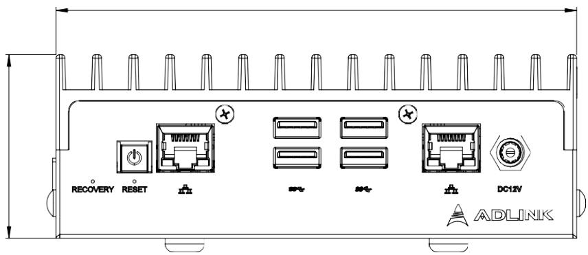
![RECOVERY\nRESET\nDC12V\nADLINK](.dlap-211-series-manual-50m-00016-1020-12/5d4834e6482aa00e9e268a0f99bb2914f7da0792c9266b1841db086edc3b114e.jpg)

Figure 1: DLAP-211-Nano/JT2/NX front view
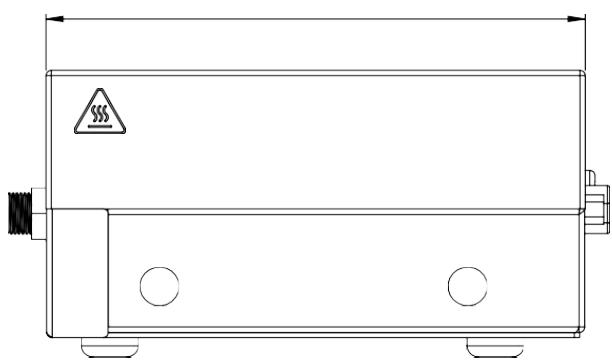
![Technical line drawing of a rectangular industrial or mechanical component with mounting holes and a warning symbol (no text or labels)](.dlap-211-series-manual-50m-00016-1020-12/55b3fd0deac2cb51e32e1f7429a2b9e951a3f34f23b4d5ca5154fc6938df0640.jpg)

Figure 2: DLAP-211-Nano/JT2/NX side view
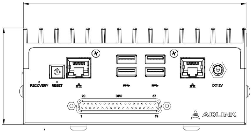
![RECOVERY RESET\n20 DVO 37\n1 19\nDC12V\nADLINK](.dlap-211-series-manual-50m-00016-1020-12/a30224d6f72819854a041a3cc7aab16203d15a73371a9112522dabd0080a53f3.jpg)

Figure 3: DLAP-211-NanoS/JT2S/NXS front view
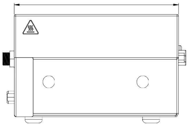
![Technical line drawing of a rectangular industrial or mechanical component with mounting holes and a warning symbol (no text or labels)](.dlap-211-series-manual-50m-00016-1020-12/6cb727b9a8aee22c141b94bf7bb7e41713cd19ffdafde3b01692e0fada645a89.jpg)

Figure 4: DLAP-211-NanoS/JT2S/NXS side view

# 4 Getting Started

# Unpacking Checklist

Before unpacking, check the shipping carton for any damage. If the shipping carton and/or contents are damaged, inform your dealer immediately. Retain the shipping carton and packing materials for inspection. Obtain authorization from your dealer before returning any product to ADLINK. Ensure that the fol- lowing items are included in the package.

 DLAP-211 unit
 Screw pack
 VESA mount kit (plus optional DIN rail kit if applicable)
 >60W Power adapter

# Cooling Considerations

All heat-generating components of the DLAP-211 are located on the left side of the system. These components directly contact the heat sink via thermal pads to dissipate heat. To maximize effi- ciency of heat dissipation, maintain a minimum of 2 inches (5cm) clearance on the top of the DLAP-211.

# Removing the Chassis Cover

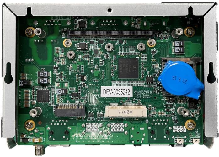
To access the DLAP-211’s internal components, remove the underside of the chassis as follows.

1. On the front panel, remove the nut and washer from the 12V DC connector and remove the two mounting screws, as indicated in the figure below.
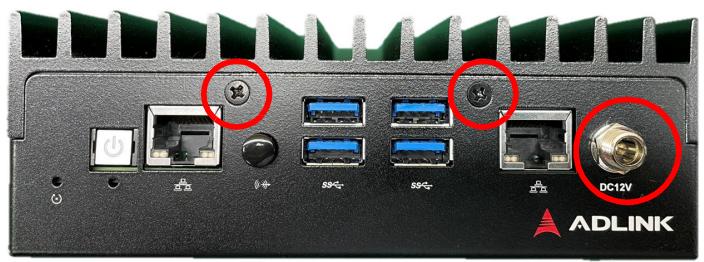
![Back panel of a network device showing ADLINK logo, ports, and connectors (no readable text or symbols beyond branding)](.dlap-211-series-manual-50m-00016-1020-12/38c9ffd13e86d2855788fe72ba2945ac58ad67b5591e4226d3d5e98e22ed93d5.jpg)

2. Remove one screw on the underside of the device.
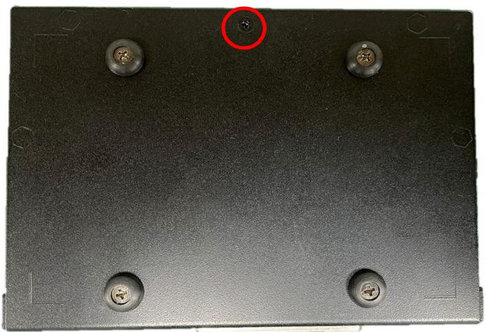
![Close-up of a black electronic component with four circular screws and a red circle highlighting a small hole (no text or symbols)](.dlap-211-series-manual-50m-00016-1020-12/05bd3ff13779b45b6a4b30bf0493a77d7ac1885d9e3b8a512fc1a3e1382b7d93.jpg)

1. Slide the cover in the direction indicated by the red arrow.
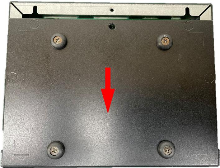
![Close-up of a black electronic device with four screws and a red arrow pointing to a surface (no text or symbols visible)](.dlap-211-series-manual-50m-00016-1020-12/76de026a6bbf421acec301dbeed6ad28481c8fe622f494ea580491de76c0198e.jpg)

2. Lift the cover off of the chassis.
![Green printed circuit board with electronic components and a blue plastic component labeled '20.5.15' (no readable text beyond label)](.dlap-211-series-manual-50m-00016-1020-12/e6cb2309ca7878a725728d9cfa718f1ee271c51d0e2cff2e0b204614cb0d50af.jpg)

Reverse the steps to replace the bottom cover.

# nstalling an M.2 SSD Module

Use the following steps to install an M.2 SSD module.

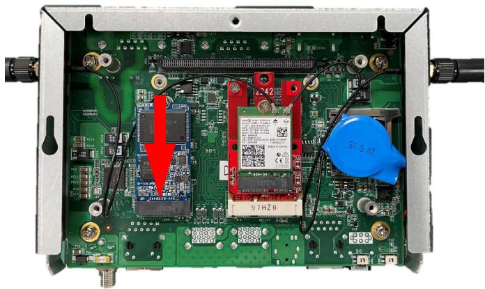
1. Insert the M.2 2242 B or B+M key module into the indi- cated slot (under the wires) at an angle.
![Interior view of an electronic device with green circuit board and red/blue component labels (no readable text or symbols)](.dlap-211-series-manual-50m-00016-1020-12/2b59719b4033cd4c9b8aaded9e50aa2717ccfbf6936b5d8aee2e1a3e49f9a3d9.jpg)

Figure 5: M.2 2242 B-key slot

2. Press down on the M.2 module until it is seated, then secure it with one M2.5-P-head-L5 screw (not provided).
3. Replace the bottom cover of the chassis.

![The image shows a yellow triangular warning sign with a black border pointing upwards. Inside the triangle is a black exclamation mark. The sign is set against a white background.](.dlap-211-series-manual-50m-00016-1020-12/b06ebe95f7a43d9718abb77f6cf47b65f94316ff066ece0dfd7ddbe5ad24b132.jpg)
CAUTION:

Make sure not to remove or damage any wires while installing the module.

# Installing a Mini PCIe Wi-Fi Module

Use the following steps to install a Mini PCIe Wi-Fi module.

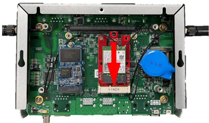
1. Insert the Mini PCIe Wi-Fi module into the indicated slot at an angle.
![Interior view of an electronic circuit board with visible components and wiring (no readable text or symbols)](.dlap-211-series-manual-50m-00016-1020-12/caad49fbd5016e912cba9266793d94ccf27a4da88d61a0bcea8ed63ce3a357a8.jpg)

Figure 6: Mini PCIe Wi-Fi slot

2. Press down on the module until it is seated, then secure it to the board using two M2.5-P-head-L5 screws (not provided).
3. Attach the wires and antennas that came with your Wi-Fi kit. It is recommended that the Wi-Fi antenna be connected to the left SMA antenna port, and Wi-Fi + Bluetooth antenna be connected to the right SMA antenna port.
4. Replace the bottom cover of the chassis.

# Connecting DC Power

![The image displays a safety warning symbol featuring a solid red, upward-pointing triangle containing a white exclamation point. Directly beneath the triangle, the word 'WARNING:' is printed in black capital letters.](.dlap-211-series-manual-50m-00016-1020-12/73da8b50da0b12ed10773e5693d983868ddfa0e58d7625150c63f447e9d6bdbf.jpg)

Before providing DC power to the DLAP-211, ensure the voltage and polarity provided are compatible with the DC input. Improper input voltage and/or polarity can be responsible for system damage.

Avant de connecter le PC DLAP-211 à une source de courant continu, veuillez vous assurer de la polarité de la tension con- formément à l'entrée CC du PC. Une tension et/ou une polarité incorrectes peuvent causer des dommages irréversibles sur le système.

DC power sources must comply with LPS and SELV (ES1) circuits with no energy hazard, as well as the following:

 IEC 62368-1, IEC 60950-1, and UL 62368-1
 Output voltage: 12V DC
 Output current: 5.0A minimum
 ${ \mathsf { T M A } } : 5 5 ^ { \circ } { \mathsf { C } }$ with DC input; $4 0 ^ { \circ } \mathsf { C }$ with adapter input
 Altitude Operability: 5000m minimum

The DLAP-211 DC power input connector uses V+, V-, and chassis ground pins.

Les sources d'alimentation CC doivent être conformes aux circuits LPS et SELV (ES1) avecaucun risque énergétique, ainsi que:

 CEI 62368-1, CEI 60950-1 et UL 62368-1
 Tension de sortie: 12V DC
 Courant de sortie: 5.0A minimum
 TMA: $5 5 \textdegree$ avec entrée $D C ; 4 0 ^ { \circ } C$ avec entrée adaptateur.
 Altitude de fonctionnement: min. 5000 mètres

Le connecteur d'entrée d'alimentation CC DLAP-211 utilise V+, V- et châssis broches de terre.

![The image depicts a graphic icon representing a document or page. It features a white shape with a folded top-left corner and several horizontal black lines running across it, simulating text. Superimposed over the document is a large, bold red checkmark that spans vertically from the top to the bottom of the page.](.dlap-211-series-manual-50m-00016-1020-12/f83becab3bc48f2515487b87bf2a9bc651c7db98246fa4af92a7fc88aede3222.jpg)
NOTE:

For additional assistance and information, contact ADLINK. To reduce potential safety hazards, use only the AC adapter pro- vided with the product, a replacement AC adapter provided by ADLINK, or an AC adapter purchased as an accessory from ADLINK.

Si vous avez besoin d'aide supplémentaire, veuillez contacter ADLINK pour plus d'informations. Pour réduire les problèmes de sécurité potentiels, seul l'adaptateur secteur fourni avec le produit, un adaptateur secteur de remplacement fourni par ADLINK ou un adaptateur secteur acheté comme accessoire auprès d'ADLINK doit être utilisé avec le produit.

# VESA Mount

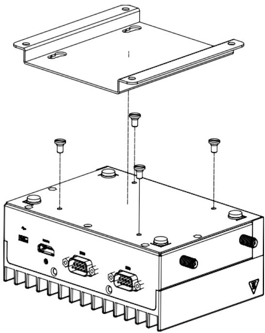
The DLAP-211 controller ships with a VESA 100 mounting bracket and four M4 screws. Follow the steps below to mount the device.

1 Attach the VESA bracket to the wall (or other suitable mounting surface) such that its keyholeshaped mounting holes are oriented with the wider openings at the top.
2 Secure the four M4 screws to the bottom of the chassis.
3 Securely attach the device to the VESA bracket by first inserting the heads of the screws into the wider openings of the VESA bracket’s mounting holes, then sliding the device down such that NOTEthe screws are now firmly held by the narrower portions of the mounting holes.

![This is an icon depicting a white document with horizontal gray lines and a folded top-right corner. A large red checkmark is superimposed over the document, indicating approval or completion. The entire graphic is enclosed within a thin black square border.](.dlap-211-series-manual-50m-00016-1020-12/3568ef460d85158e9f7413abe5eba1270aadc85e2c1d4a3453f92a4dbca4a0e5.jpg)
NOTE:

It is recommended that four M4 screws, 6cm in length, be used to attach the assembled brackets to a wall. Actual fastener type and length will be determined by the type of wall being anchored to. (Sample anchors M4x0.7 L8mm with washer.)
![Technical line drawing of an electronic device showing internal components and mounting points (no text or symbols)](.dlap-211-series-manual-50m-00016-1020-12/acb2877e0bd4cfda87a96848067fce9ddba5eafb13ef5ef514b48cc396ec1613.jpg)

Figure 7: VESA mount

# DIN Rail Mount

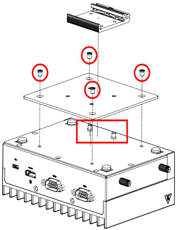
The DLAP-211 controller may optionally include a DIN rail mount kit, with its own six M4 screws, in addition to the standard VESA mount kit. Follow these steps to install the DIN rail bracket.

1. Use two M4 screws (pointing upwards in the red box below) to attach the DIN rail bracket to the adapter plate.
2. Use four M4 screws (circled in red below) to attach the DIN rail bracket assembly to the DLAP-211 chassis.
![Technical diagram of an electronic device with labeled components and red circles highlighting specific ports or features.](.dlap-211-series-manual-50m-00016-1020-12/2f8567f78c90737b25515ea7c9d3711d936372ead373501433885f73a12438d5.jpg)

Figure 8: DIN rail mount

# AT Power Mode Switch (SW4)

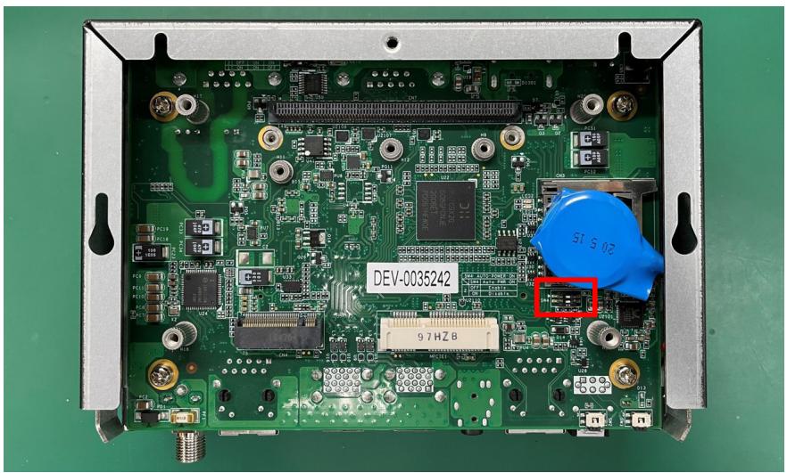
The DLAP-211 is set in AT mode by default. By using the AT Power Mode Switch (SW4), users can set the system to be powered-on with the power button.
![Interior view of an electronic circuit board with visible components and a highlighted blue component (no readable text or symbols)](.dlap-211-series-manual-50m-00016-1020-12/8f693f0b3eb5dbaac3b815780ebede11298fc74633205d0b7829845cb05aedeb.jpg)

Figure 9: AT power mode switch (SW4)

AT mode can be configured as follows:

Table 1: AT mode switch configuration

<table><tr><td colspan="3">SW4 Auto Power On</td></tr><tr><td></td><td>SW4</td><td>Auto Power On</td></tr><tr><td rowspan="2">2</td><td>OFF</td><td>Enable (Default)</td></tr><tr><td>ON</td><td>Disable</td></tr></table>

This page intentionally left blank.

# 5 System Layout

# Front Panel I/O Connectors

DLAP-211-NanoS/JT2S/NXS Front Panel

![RECOVERY\nRESET\nA\nDC12V\nADLINK\nB C D E D F](.dlap-211-series-manual-50m-00016-1020-12/6d5deb90367ceef432f209c6ec9e2b40e36b64caa987c0023c58f62503d20885.jpg)

Figure 10: DLAP-211-NanoS/JT2S/NXS front panel I/O connectors 1

DLAP-211-NanoS/JT2S/NXS Front Panel

![RECOVERY RESET\n20 DVO 37\n1 10\nDC12V\nADLINK\nG](.dlap-211-series-manual-50m-00016-1020-12/4ec2f778f28c02a487e17ac83487b3713d6b7cf8a0f9457dfa63f9db380d0f61.jpg)

Figure 11: DLAP-211-NanoS/JT2S/NXS front panel I/O connectors 2

Table 2: Front panel I/O connector descriptions

<table><tr><td>Item</td><td>Name</td><td>Description</td></tr><tr><td>A</td><td>Power button</td><td>The power button is a non-latched pushbutton with a blue LED power indicator. Press to power on/power off the system. The button LED lights up when the system is turned on. If the system hangs, pressing and holding the button continuously for 5 seconds performs a hard shutdown on the system.</td></tr><tr><td>B</td><td>Recovery button</td><td>Press this button to force the system into recovery mode. See Section 3.2 System Recovery.</td></tr><tr><td>C</td><td>Reset button</td><td>The reset button executes a hard reset on the system.</td></tr><tr><td>D</td><td>GbE connector (LAN 1)</td><td>GbE from NVIDIA® JetsonTM modules.See Section 1.5 Pin Definitions.</td></tr><tr><td>D</td><td>GbE connector (LAN 2)</td><td>GbE from Intel® I210.See Section 1.5 Pin Definitions.</td></tr><tr><td>E</td><td>USB 3.0</td><td>See Section 1.5.2 USB 3.0 Connectors.</td></tr><tr><td>F</td><td>DC connector 12V</td><td>12V DC screw-type connector.See Section 1.5.3 12V DC Connector.</td></tr><tr><td>G</td><td>D-sub 37-pin connector</td><td>1x I2C, 1x SPI, 1x UART, 8x GPIO, 1x Relay function</td></tr></table>

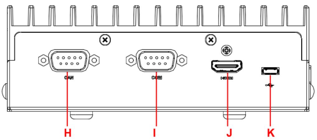
# Rear Panel I/O Connectors

![CAN\nCOM\nH\nI\nJ\nK](.dlap-211-series-manual-50m-00016-1020-12/08279bfdd421b93d35a7fac52ad5a9055f4580b8a6543c6c478bf6073abaee51.jpg)

Figure 12: Rear panel I/O connectors

Table 3: Rear panel descriptions

<table><tr><td>Item</td><td>Name</td><td>Description</td></tr><tr><td>H</td><td>CAN bus</td><td>CAN 2.0B (backward compatible with 2.0A)</td></tr><tr><td>I</td><td>Serial port</td><td>COM port (DB-9 connector)RS-232/422/485 (software programmable)</td></tr><tr><td>J</td><td>HDMI port</td><td>HDMI 2.0 with lock</td></tr><tr><td>K</td><td>USB 2.0</td><td>USB 2.0 OTG (Micro USB)</td></tr></table>

# 6 Connector Pinouts and Jumper Settings

# Ethernet GbE Connectors

The DLAP-211 series comes with two RJ45 connectors:

NVIDIA® Jetson™ modules (LAN 1)
Intel® I210 (LAN 2)

LAN LED connection speed color indicators:

<table><tr><td></td><td>Active &amp; Link(Left LED)</td><td>Speed(Right LED)</td></tr><tr><td>10 Mbps</td><td>Yellow (Blinking)</td><td>N/A</td></tr><tr><td>100 Mbps</td><td>Yellow (Blinking)</td><td>N/A</td></tr><tr><td>1000 Mbps</td><td>Yellow (Blinking)</td><td>Green</td></tr></table>

The following table provides details for the RJ45 GbE pin connections.

<table><tr><td>Pin #</td><td>10BASE-T/100BASE-TX</td><td>1000BASE-T</td></tr><tr><td>1</td><td>TX+</td><td>LAN_TX0+</td></tr><tr><td>2</td><td>TX-</td><td>LAN_TX0-</td></tr><tr><td>3</td><td>RX+</td><td>LAN_TX1+</td></tr><tr><td>4</td><td>—</td><td>LAN_TX2+</td></tr><tr><td>5</td><td>—</td><td>LAN_TX2-</td></tr><tr><td>6</td><td>RX-</td><td>LAN_TX1-</td></tr><tr><td>7</td><td>—</td><td>LAN_TX3+</td></tr><tr><td>8</td><td>—</td><td>LAN_TX3-</td></tr></table>

# USB 3.0 Connectors

The USB 3.0 ports support a USB Type-A connection, compatible with SuperSpeed, Hi-Speed, Full-speed, and Low-speed USB devices suitable for USB peripherals including USB cameras.

<table><tr><td>Pin #</td><td>Signal Name</td></tr><tr><td>1</td><td>USB3.0_P5VA</td></tr><tr><td>2</td><td>USB2_CMAN</td></tr><tr><td>3</td><td>USB2_CMAP</td></tr><tr><td>4</td><td>GND</td></tr><tr><td>5</td><td>USB3A_CMRXN</td></tr><tr><td>6</td><td>USB3A_CMRXP</td></tr><tr><td>7</td><td>GND</td></tr><tr><td>8</td><td>USB3A_CMTXN</td></tr><tr><td>9</td><td>USB3A_CMTXP</td></tr></table>

![1\n2\n3\n4\n5\n6\n7\n8\n9](.dlap-211-series-manual-50m-00016-1020-12/ea2c943e88d0b94a1ab7744993437f0dfd7d6e8084dd188e5d3a0390a1161f8f.jpg)

# 12V DC Connector

The system requires a 12V DC power source with a screw-type connector.

![+12V\nGND](.dlap-211-series-manual-50m-00016-1020-12/a252da14b8140e38e040166032c7f75a860ddb7d564e4521d4f8275786b7a490.jpg)

![12.5±0.3\n3.0\n+0.1\nφ5.6-0\n+0.2\n2.6-0](.dlap-211-series-manual-50m-00016-1020-12/a551affab6eb255df88678233707b8cad1d474b187bb47591707b9e3d2049b70.jpg)

# Controller Area Network (CAN) Bus

The Controller Area Network (CAN) enables communication among devices.

<table><tr><td>Pin</td><td>Signal</td><td>Description</td></tr><tr><td>1</td><td>NC</td><td>(Not connected)</td></tr><tr><td>2</td><td>CAN0_Low</td><td>Differential CAN signal negative level</td></tr><tr><td>3</td><td>NC</td><td>(Not connected)</td></tr><tr><td>4</td><td>NC</td><td>(Not connected)</td></tr><tr><td>5</td><td>NC</td><td>(Not connected)</td></tr><tr><td>6</td><td>NC</td><td>(Not connected)</td></tr><tr><td>7</td><td>CAN0_High</td><td>Differential CAN signal positive level</td></tr><tr><td>8</td><td>NC</td><td>(Not connected)</td></tr><tr><td>9</td><td>NC</td><td>(Not connected)</td></tr></table>

![6\n1\n5](.dlap-211-series-manual-50m-00016-1020-12/a008a9833756e112e8d973d20a067b6ca952689973483424d21d792921f1bfd2.jpg)

# COM Port

One COM port supports RS-232/422/485.

<table><tr><td>Pin</td><td>RS-232</td><td>RS-422</td><td>RS-485</td></tr><tr><td>1</td><td>DCD#</td><td>COM_TXD_N</td><td>COM_D-</td></tr><tr><td>2</td><td>COM_RXD</td><td>COM_TXD_P</td><td>COM_D+</td></tr><tr><td>3</td><td>COM_TXD</td><td>COM_RXD_P</td><td>NC</td></tr><tr><td>4</td><td>DTR#</td><td>COM_RXD_N</td><td>NC</td></tr><tr><td>5</td><td>COM_GND</td><td>NC</td><td>NC</td></tr><tr><td>6</td><td>NC</td><td>NC</td><td>NC</td></tr><tr><td>7</td><td>COM_RTS#</td><td>NC</td><td>NC</td></tr><tr><td>8</td><td>COM_RCTS#</td><td>NC</td><td>NC</td></tr><tr><td>9</td><td>NC</td><td>NC</td><td>NC</td></tr></table>

# HDMI Connectors

The rear panel HDMI connector supports HDMI 2.0.

<table><tr><td>Pin #</td><td>Signal</td><td>Pin #</td><td>Signal</td></tr><tr><td>1</td><td>TMDS Data2+</td><td>2</td><td>TMDS Data2 Shield</td></tr><tr><td>3</td><td>TMDS Data2-</td><td>4</td><td>TMDS Data1+</td></tr><tr><td>5</td><td>TMDS Data1 Shield</td><td>6</td><td>TMDS Data1-</td></tr><tr><td>7</td><td>TMDS Data0+</td><td>8</td><td>TMDS Data0 Shield</td></tr><tr><td>9</td><td>TMDS Data0-</td><td>10</td><td>TMDS Clock+</td></tr><tr><td>11</td><td>TMDS Clock Shield</td><td>12</td><td>TMDS Clock-</td></tr><tr><td>13</td><td>CEC</td><td>14</td><td>Reserved</td></tr><tr><td>15</td><td>SCL</td><td>16</td><td>SDA</td></tr><tr><td>17</td><td>DDC/CEC Ground</td><td>18</td><td>+5 V Power</td></tr><tr><td>19</td><td>Hot Plug Detect</td><td></td><td></td></tr></table>

![The image displays a technical diagram of a rectangular connector, specifically a 25-pin D-sub connector (DB25). It features a gray body with two rows of circular pinholes and small square mounting holes at the corners. Numbers are arranged around the connector to indicate pin positions:\n\n*   **Left side:** The numbers **19**, **17**, and **18** are stacked vertically near the left end of the connector.\n*   **Right side:** The numbers **3** and **1** are near the top right, and **4** and **2** are stacked vertically below them on the right side.](.dlap-211-series-manual-50m-00016-1020-12/e3470e3b94220869b363bb72aface2d7f3b2b8b83988fdf1d4df7ebe6cc22bf6.jpg)

# USB 2.0 OTG Connector

The DLAP-211 supports a USB 2.0 OTG Micro USB Type-B connection for system recovery.

<table><tr><td>Pin</td><td>Signal</td><td>Description</td></tr><tr><td>1</td><td>VCC_USBDev</td><td>USB device power</td></tr><tr><td>2</td><td>USB_D1_n</td><td rowspan="2">Universal Serial Bus Port 1 / USB-Client differential pair</td></tr><tr><td>3</td><td>USB_D1_p</td></tr><tr><td>4</td><td>USB_ID</td><td>USB ID pin</td></tr><tr><td>5</td><td>GND_USBDev</td><td>USB GND</td></tr></table>

# D-sub 37-pin Connector

<table><tr><td>Pin #</td><td>Signal</td><td>Voltage</td><td>Pin #</td><td>Signal</td><td>Voltage</td></tr><tr><td>1</td><td>OPEN Relay</td><td></td><td>2</td><td>N/A</td><td></td></tr><tr><td>3</td><td>COM Relay</td><td></td><td>4</td><td>N/A</td><td></td></tr><tr><td>5</td><td>SPI0_SCK</td><td>3.3V</td><td>6</td><td>SPI0_CS1_1</td><td>3.3V</td></tr><tr><td>7</td><td>SPI0_MOSI</td><td>3.3V</td><td>8</td><td>SPI0_MISO</td><td>3.3V</td></tr><tr><td>9</td><td>SPI0_CS0_L</td><td>3.3V</td><td>10</td><td>GND</td><td></td></tr><tr><td>11</td><td>(GPO1)GPIO_14</td><td>3.3V</td><td>12</td><td>(GPO2)GPIO_12</td><td>3.3V</td></tr><tr><td>13</td><td>(GPO3)GPIO_10</td><td>3.3V</td><td>14</td><td>(GPO4)GPIO_06</td><td>3.3V</td></tr><tr><td>15</td><td>(GPI1)GPIO_05</td><td>3.3V</td><td>16</td><td>(GPI2)GPIO_04</td><td>3.3V</td></tr><tr><td>17</td><td>(GPI3)GPIO_03</td><td>3.3V</td><td>18</td><td>(GPI4)GPIO_02</td><td>3.3V</td></tr><tr><td>19</td><td>GND</td><td></td><td>20</td><td>GND</td><td></td></tr><tr><td>21</td><td>JUMPER2_EN</td><td></td><td>22</td><td>GPIO_07</td><td></td></tr><tr><td>23</td><td>I2C0_SDA</td><td>3.3V</td><td>24</td><td>I2C0_SCL</td><td>3.3V</td></tr><tr><td>25</td><td>GND</td><td></td><td>26</td><td>GND</td><td></td></tr><tr><td>27</td><td>3.3V</td><td></td><td>28</td><td>3.3V</td><td></td></tr><tr><td>29</td><td>GND</td><td></td><td>30</td><td>UART0_RTS</td><td>3.3V</td></tr><tr><td>31</td><td>UART0_CTS</td><td>3.3V</td><td>32</td><td>UART0_TXD</td><td>3.3V</td></tr><tr><td>33</td><td>UART0_RXD</td><td>3.3V</td><td>34</td><td>GND</td><td></td></tr><tr><td>35</td><td>GND</td><td></td><td>36</td><td>5V</td><td></td></tr><tr><td>37</td><td>5V</td><td></td><td></td><td></td><td></td></tr></table>

![19\n37\n20\n1](.dlap-211-series-manual-50m-00016-1020-12/d01290cbe558fe2b3710e0e9c514bde22b15ae2e75041e195816ab7adbb82bae.jpg)

# Side I/O Slots

The I/O connectors accessible from the right side panel of the DLAP-211 are described below.

![Technical line drawing of a device casing with labeled ports and internal components (no readable text or symbols)](.dlap-211-series-manual-50m-00016-1020-12/47afb9cdf79160d0fa66929e2694412a6e37aff8f6654b23e4c10486530c3ae9.jpg)

# SD Card Slot

For additional storage, use the side door to install or remove a user-provided SD card.

# USIM Slot

The DLAP-211 is equipped with a USIM slot connected to the Mini PCIe connector for use with a user-provided SIM card and 3G/4G Mini PCIe module to provide cellular communication. Install or remove a SIM card module via the side door.

![The image displays a white document icon with a folded top-right corner. Faint grey horizontal lines are visible on the right side, simulating text. A large, bold red checkmark is superimposed diagonally across the center of the document.](.dlap-211-series-manual-50m-00016-1020-12/5f074615c0da64996337fdecbc75aff1053b19f231d469d68553f82b0169c678.jpg)
NOTE:

The 3G/4G Mini PCIe module requires a user-provided SIM card for communication via a telecom operator. See Section 4.5 Installing a Mini PCIe Wi-Fi Module.

# Orientation

Insert the SIM and SD cards with the orientations shown below.

![Close-up of a black electronic device with a microSD adapter and a small white chip, placed on a green surface (no visible text or symbols)](.dlap-211-series-manual-50m-00016-1020-12/4207dd52d131bbe21966c9d53b9e4b11088bfc7aba61cdc367388ef90966eb52.jpg)

# 7 Using the System

# Software Configuration

The DLAP-211 ships with a customized NVIDIA Linux for Tegra (L4T) image pre-installed. The latest version of this custom L4T image and other relevant files are available on the ADLINK web- site.

DLAP-211-JNX:

https://www.adlinktech.com/Products/Deep\_Learning\_Accelerator

\_Platform\_and\_Server/Inference\_Platform/DLAP-211-JNX

DLAP-211-JT2:

https://www.adlinktech.com/Products/Deep\_Learning\_Accelerator

\_Platform\_and\_Server/Inference\_Platform/DLAP-211-JT2

DLAP-211-Nano:

https://www.adlinktech.com/Products/Deep\_Learning\_Accelerator

\_Platform\_and\_Server/Inference\_Platform/DLAP-211-Nano

# Flash the System Image

Before flashing the image to NVIDIA Jetson Family, you should prepare the following items:

1. A Host PC with Ubuntu operating system.

2. A good quality OTG cable (micro-usb/USB type C) for connecting it to NVIDIA Jetson Family (Client PC).

Complete the following steps on the Client PC before performing the host PC steps:

# Client PC

1. Connect the OTG cable to the USB port.

2. Enter Recovery Mode

# Method 1: (Power on)

\$ sudo reboot --force forced-recovery

# Method 2: (Power off)

1. Press and hold the recovery button.

2. Press the power switch.

3. Press the reset button once and release it after 3-5 seconds.

# Recovery button

![RECOVERY RESET](.dlap-211-series-manual-50m-00016-1020-12/be5c11bf746db184ef7cca0944b7870d261659ff567098b994ea25ac9d6529d5.jpg)

# Recovery button on development kit

![Recovery button](.dlap-211-series-manual-50m-00016-1020-12/199b84d526dab64d6d4ed7ad5d7e00f11c60488b84d478a2251c16e6b280b006.jpg)

# Host PC

The host must have the following dependencies:

\$ sudo apt install libxml2-utils simg2img network-manager abootimg sshpass device-treecompiler nfs-kernel-server

1. Connect the host PC to the Client PC via OTG cable.

2. Open a terminal, run the following command and check out the mode on the host PC:

\$ lsusb | grep NVIDIA

<table><tr><td>Recovery mode will show APX.</td><td>Normal mode will show L4T.</td></tr><tr><td></td><td></td></tr><tr><td>Bus 001 Device 031: ID 0955:7019 NVIDIA Corp. APX</td><td>Bus 001 Device 030: ID 0955:7020 NVIDIA Corp. L4T (Linux for Tegra) running on Tegra</td></tr></table>

• We need to make sure the client PC in recovery mode before flash image.

If client PC doesn't recognize or not in recovery mode, double-check the OTG cable connection and perform troubleshooting as needed until the client is recognized and in recovery mode.

3. Download the mfi file image into the Host PC.

ex: mfi\_jetson-orin-nano-dlap211-onx\_16-35.3.1-2v1.2.tbz2

4. Unzip the mfi file that was previously downloaded.

ex: \$ sudo tar -jxf mfi\_jetson-orin-nano-dlap211-onx\_16-35.3.1-2v1.2.tbz2

5. Go to the working folder.

ex: \$ cd mfi\_jetson-orin-nano-dlap211-onx\_16-35.3.1-2v1.2

6. Execute the flash command

ex: \$ sudo ./tools/kernel\_flash/l4t\_initrd\_flash.sh --flash-only

![The image features a white document icon with horizontal lines and a large red checkmark overlaid on it.](.dlap-211-series-manual-50m-00016-1020-12/7d1d7f482c61dd9a1b149f8f28c7b77a7abe691cabfa3a0280393dbfb67b3079.jpg)
NOTE:

In JetPack 5.0.2 and earlier versions of the MFI image, please execute the flash command:

\$ sudo ./nvmflash.sh

The following illustrates how to do the mass flash.

1. Connect Client PCs to the Host PC.

![Computer setup with electronic circuit boards and a rack-mounted server unit (no visible text or symbols)](.dlap-211-series-manual-50m-00016-1020-12/061b1763673a6c1250b19d64104ea4516969cd2c2bc24b6a0a11b078e702b4b4.jpg)

2. In the terminal, run lsusb to check that all Client PCs have entered into Recovery Mode.

![adlink@adlink-AVBX-6000: ~\$\nadlink@adlink-AVBX-6000:~\$\nadlink@adlink-AVBX-6000:~\$ lsusb\nBus 002 Device 001: ID 1d6b:0003 Linux Foundation 3.0 root hub\nBus 001 Device 062: ID 046d:c52b Logitech, Inc. Unifying Receiver\nBus 001 Device 045: ID 062a:4102 MosArt Semiconductor Corp. 2.4G Wireless Mouse\nBus 001 Device 064: ID 0955:7323 NVIDIA Corp. APX\nBus 001 Device 063: ID 0955:7323 NVIDIA Corp. APX\nBus 001 Device 001: ID 1d6b:0002 Linux Foundation 2.0 root hub\nadlink@adlink-AVBX-6000:~\$](.dlap-211-series-manual-50m-00016-1020-12/177b1779bef18a69e29546ef70383a5124164debdaa156b3375bdc2af36a764c.jpg)

# 3. Execute flash command,

\$ sudo ./tools/kernel\_flash/l4t\_initrd\_flash.sh --flash-only --massflash 2 (2 as number of client PCs need flash)

Reference:

![adlink@adlink-AVBX-6000:~/Desktop/mfl_jetson-orin-nano-dlap211-onx_16-35.3.1-2v1.2\$ sudo ./tools/kernel_flash/l4t_initrd_flash.sh\n--help\n(sudo) password for adlink:\n\nUsage: ./tools/kernel_flash/l4t_initrd_flash.sh (options) (board-name) (rootdev)\n\nWhere,\n\n-u (PKC key file) PKC key used for odom fused board.\n-v (SBK key file) SBK key used for encryptions\n-p (option) Pass options to flash.sh when generating the image for internal storage\n-k (target_partition) Only flash partition specified with the label (target_partition)\n(board-name) Indicate which board to use.\n(rootdev) Indicate what root device to use\n--no-flash Generate the flash images\n--flash-only Flash using existing images\n--external-device (dev) Generate and/or flash images for the indicated external storage\ndevice. If this is used, -c option must be specified.\n--external-only Skip generating internal storage images\n--usb-instance Specify the usb port where the flashing cable is plugged (i.e 1-3)\n--sparse Use sparse image to flash instead of tar image.\n-c (config file) The partition layout for the external storage device.\n-S (size) External APP partition size in bytes. KIB, MIB, GIB short hands are allowed,\nfor example, 1GIB means 1024 * 1024 * 1024 bytes. (optional)\n--massflash ((max_devices))\n--showlogs Spawn ghome-terminal to show individual flash process logs. Applicable\nfor --massflash only.\n--reuse Reuse existing working environment kept by --keep option.\n--keep Keep working environment instead of cleaning up after flashing\n--erase-all Delete all storage device before flashing\n--initrd Stop after device boot into initrd.\n--network (netargs) Flash through Ethernet protocol using initrd flash. (netargs) can be 'usb0' to flash through the\nUSB Flashing cable or 'eth0:(target-ip)/(subnet):(host-ip)(:(gateway)) ' to flash through the LAN cable\nFor examples:\n--network usb0\n--network eth0:192.168.0.17/24:192.168.0.21\n--network eth0:192.168.0.17/24:192.168.1.2:192.168.0.1\n\n--append Only applicable when using with --no-flash --external-only option. This option is parts of\nthe three steps flashing process to generate images for internal device and external device sepe\nrately and flash them together.\nFor examples:\n1. sudo ./tools/kernel_flash/l4t_initrd_flash.sh --no-flash jetson-xavier internal\n2. sudo ./tools/kernel_flash/l4t_initrd_flash.sh --no-flash --external-device nvme0nip1 -S 512000\n0000 -c flash_enc.xml --external-only --append jetson-xavier internal\n3. sudo ./tools/kernel_flash/l4t_initrd_flash.sh --flash-only jetson-xavier internal\n\n--direct (dev) Flash the device directly connected to host with the (dev) name\nFor examples,\nsudo ./tools/kernel_flash/l4t_initrd_flash.sh --direct sdb --external-device sda -c flash_extern\nal.xml concord sda1\n\n--user_key (key_file) User provided key file (16-byte) to encrypt user images, like kernel, kernel-dtb and initrd.\nIf user_key is specified, SBK key (-v) has to be specified.\nFor now, user_key file must contain all 0's.\n\n--pv-crt (crt file) The certificate for the key that is used to sign cpu_bootloader\n\nWith --external-device options specified, the supported values for (dev) are\nnvme0n1\nsda](.dlap-211-series-manual-50m-00016-1020-12/b83b6898d3c08454ac7fa95d4e7844a1120ed5923ac9a8fde1bd7c6ae545518b.jpg)

# COM Port Configuration

By default, the DLAP-211 is configured to support the RS-232 pro- tocol.

<table><tr><td>Model</td><td>COM Port Name</td></tr><tr><td>DLAP-211-JNX/JNXS</td><td>ttyTHS0</td></tr><tr><td>DLAP-211-JT2/JT2S</td><td>ttyTHS2</td></tr><tr><td>DLAP-211-Nano/NanoS</td><td>ttyTHS1</td></tr></table>

Switching between RS-232/422/485:

```shell
echo rs232 > /sys/class/sp339_mode_ctl/uartMode
echo rs422 > /sys/class/sp339_mode_ctl/uartMode
echo rs485 > /sys/class/sp339_mode_ctl/uartMode
```

Checking the current mode of the serial port:

```txt
cat /sys/class/sp339_mode_ctl/uartMode
```

# SPI, I2C, and Relay Configuration

The DLAP-211-JT2S, DLAP-211-NanoS, and DLAP-211-JNXS

support I2C, SPI, GPIO, and Relay functions through a 37-pin D- sub connector that can be accessed through the commands described in the following sections.

# GPIO

DLAP-211-JNXS GPIO map table:

<table><tr><td>Pin</td><td>Signal</td><td>GPIO Number</td><td>Pin</td><td>Signal</td><td>GPIO Number</td></tr><tr><td>11</td><td>GPO 1</td><td>gpio345</td><td>15</td><td>GPI 1</td><td>gpio266</td></tr><tr><td>12</td><td>GPO 2</td><td>gpio268</td><td>16</td><td>GPI 2</td><td>gpio265</td></tr><tr><td>13</td><td>GPO 3</td><td>gpio417</td><td>17</td><td>GPI 3</td><td>gpio264</td></tr><tr><td>14</td><td>GPO 4</td><td>gpio267</td><td>18</td><td>GPI 4</td><td>gpio419</td></tr></table>

DLAP-211-JT2S GPIO map table:

<table><tr><td>Pin</td><td>Signal</td><td>GPIO Number</td><td>Pin</td><td>Signal</td><td>GPIO Number</td></tr><tr><td>11</td><td>GPO 1</td><td>gpio278</td><td>15</td><td>GPI 1</td><td>gpio408</td></tr><tr><td>12</td><td>GPO 2</td><td>gpio338</td><td>16</td><td>GPI 2</td><td>gpio411</td></tr><tr><td>13</td><td>GPO 3</td><td>gpio337</td><td>17</td><td>GPI 3</td><td>gpio410</td></tr><tr><td>14</td><td>GPO 4</td><td>gpio340</td><td>18</td><td>GPI 4</td><td>gpio409</td></tr></table>

DLAP-211-NanoS GPIO map table:

<table><tr><td>Pin</td><td>Signal</td><td>GPIO Number</td><td>Pin</td><td>Signal</td><td>GPIO Number</td></tr><tr><td>11</td><td>GPO 1</td><td>gpio39</td><td>15</td><td>GPI 1</td><td>gpio63</td></tr><tr><td>12</td><td>GPO 2</td><td>gpio194</td><td>16</td><td>GPI 2</td><td>gpio65</td></tr><tr><td>13</td><td>GPO 3</td><td>gpio169</td><td>17</td><td>GPI 3</td><td>gpio66</td></tr><tr><td>14</td><td>GPO 4</td><td>gpio64</td><td>18</td><td>GPI 4</td><td>gpio62</td></tr></table>

# Examples:

GPO set low command:

\$echo 0 > /sys/class/gpio/gpio345/value

GPI get value command:

\$cat /sys/class/gpio/gpio266/value

# SPI, I2C, Relay

DLAP-211-JNXS/JT2S/NanoS SPI, I2C, Relay map table:

<table><tr><td>Model</td><td>I2C Name</td><td>SPI Name</td><td>Relay GPIO Number</td></tr><tr><td>DLAP-211-JNXS</td><td>i2c1</td><td>/dev/spidev0.0 /dev/spidev0.1</td><td>gpio424</td></tr><tr><td>DLAP-211-JT2S</td><td>i2c2</td><td>/dev/spidev0.0 /dev/spidev0.1</td><td>gpio264</td></tr><tr><td>DLAP-211-NanoS</td><td>i2c3</td><td>/dev/spidev0.0 /dev/spidev0.1</td><td>gpio168</td></tr></table>

# Safety Instructions

For user safety, please read and follow all instructions, Warnings, Cautions, and Notes marked in this manual and on the associated device before handling/operating the device, to avoid injury or damage.

S'il vous plaît prêter attention stricte à tous les avertissements et mises en garde figurant sur l'appareil , pour éviter des blessures ou des dommages.

► Read these safety instructions carefully.
► Keep the User’s Manual for future reference.
► Read the Specifications section of this manual for detailed information on the recommended operating environment.
► When installing/mounting or uninstalling/removing device; or when removal of a chassis cover is required for user servicing (See “Getting Started”):

[> Turn off power and unplug any power cords/cables.

[> Reinstall all chassis covers before restoring power.

► To avoid electrical shock and/or damage to device:

[> Keep device away from water or liquid sources.
[> Keep device away from high heat or humidity.
[> Keep device properly ventilated (do not block or cover ventilation openings).
[> Always use recommended voltage and power source settings.
[> Always install and operate device near an easily accessible electrical outlet.
[> Secure the power cord (do not place any object on/over the power cord) and connect it to a socket-outlet with earthing connection.
[> Only install/attach and operate device on stable surfaces and/or recommended mountings.

► If the device will not be used for long periods of time, turn off and unplug from its power source.
► Never attempt to repair the device, which should only be serviced by qualified technical personnel using suitable tools.
► A Lithium-type battery may be provided for uninterrupted backup or emergency power.

![A cropped image showing the bottom portion of a yellow triangular warning sign with a black border. Inside the triangle is a large black exclamation point. Thin horizontal black lines appear at the very top and bottom edges of the frame.](.dlap-211-series-manual-50m-00016-1020-12/9affadc303a0f0b88c155fa5e42566251eaaef011e54be3815e60222d96aae09.jpg)
CAUTION:

Risk of explosion if battery is replaced with one of an incorrect type; please dispose of used batteries appropriately.

Risque d’explosion si la pile est remplacée par une autre de type incorrect. Veuillez jeter les piles usagées de façon appropriée.

► The device must be serviced by authorized technicians when:

[> The power cord or plug is damaged.
[> Liquid has entered the device interior.
[> The device has been exposed to high humidity and/or moisture.
[> The device is not functioning or does not function according to the User’s Manual.
[> The device has been dropped and/or damaged and/or shows obvious signs of breakage.

► Disconnect the power supply cord before loosening the thumbscrews and always fasten the thumbscrews with a screwdriver before starting the system up.

[> The equipment is not intended to be installed or used in a home, school, or public area accessible to the general population.
[> The knurled thumb screws with slotted heads for each Node module should be tightened with a tool after both initial installation and subsequent use.

► It is recommended that the device be installed only in a server room or computer room where access is:

[> Restricted to qualified service personnel or users familiar with restrictions applied to the location, reasons therefore, and any precautions required.
[> Only afforded by the use of a tool or lock and key, or other means of security, and controlled by the authority responsible for the location.

► Please use an approved power source certified by IEC or UL. If you need an adapter, optional accessories, or further assistance, please contact ADLINK for more information.

![The image displays a triangular warning sign with a yellow background and a thick black border. Inside the triangle is a black symbol depicting three wavy vertical lines rising above a horizontal line, indicating a hot surface.](.dlap-211-series-manual-50m-00016-1020-12/f1b11a4438142ddcf7771127c58a5da0764723b1019d68b228155c4a528300f4.jpg)

# BURN HAZARD

Touching this surface could result in bodily injury. To reduce risk, allow the surface to cool before touching.

# RISQUE DE BRÛLURES

Ne touchez pas cette surface, cela pourrait entraîner des blessures. Pour éviter tout danger, laissez la surface refroidir avant de la toucher.

► Lisez attentivement ces consignes de sécurité
► Conservez le manuel de l'utilisateur pour pouvoir le consulter ultérieurement
Lisez la section Spécifications de ce manuel pour des informations détaillées sur l'environnement d'exploitation recommandé
Lors de l'installation/montage ou de la désinstallation/retrait de l'appareil ; ou lorsque le retrait d'un boîtier est nécessaire pour l'entretien par l'utilisateur (voir Mise en route) :
► Éteignez l'alimentation et débranchez tous les cordons/câbles d'alimentation.
► Réinstallez tous les panneaux du boîtier avant de remettre l'alimentation sous tension.
► Pour éviter les chocs électriques et/ou d’endommager l’appareil :

► Tenez l'appareil à l'écart de toute source d'eau ou de liquide
► Tenez l'appareil à l'écart d'une forte chaleur ou d'une humidité élevée
► Maintenez l'appareil correctement ventilé (n'obstruer ou ne couvrez pas les ouvertures de ventilation)
► Utilisez toujours les réglages de tension et de source d'alimentation recommandés
► Installez et utilisez toujours l'appareil près d'une prise de courant facilement accessible
Fixez le cordon d'alimentation (ne placez aucun objet sur/au-dessus du cordon d'alimentation) et connectez-le à une prise de courant avec mise à la terre

► N'essayez jamais de réparer l'appareil, qui doit être réparé uniquement par du personnel technique qualifié et utilisant des outils appropriés.

► Lors de l'installation/montage ou de la désinstallation/retrait d'un périphérique, ou lorsque le retrait d'un couvercle de châssis est requis pour l'entretien par l'utilisateur :
► Coupez l’alimentation et débranchez tous les cordons/câbles d’alimentation.

► Réinstallez tous les capots du châssis avant de rétablir l'alimentation. Installez/fixez et utilisez l'appareil uniquement sur des surfaces stables et/ou des supports recommandés.

► Si l'appareil n'est pas utilisé pendant une longue période, éteignez-le et débranchez-le de sa source d'alimentation.

► Une batterie de type lithium peut être fournie pour une alimentation de secours ou de secours ininterrompue.

► L'appareil doit être réparé par des techniciens agréés lorsque :
► Le cordon d'alimentation ou la fiche est endommagé.
► Du liquide est entré dans l’appareil. € L'appareil a été exposé à une humidité élevée et/ou à l'humidité.
► L'appareil ne fonctionne pas ou ne fonctionne pas conformément au manuel de l'utilisateur.

► L'appareil est tombé et/ou a été endommagé et/ou présente des signes évidents de casse.
► Débranchez le cordon d'alimentation avant de desserrer les vis moletées et fixez toujours les vis moletées avec un tournevis avant de démarrer le système.
L'équipement n'est pas destiné à être installé ou utilisé dans une maison, une école ou une zone publique accessible au grand public.
Les vis à molette avec têtes fendue pour chaque module Node doivent être serrées avec un outil après l'installation initiale et lors de l'utilisation suivante.
► Il est recommandé d'installer l'appareil uniquement dans une salle de serveurs ou une salle informatique dont l'accès est :

Réservé au personnel de service qualifié ou aux utilisateurs familiers avec les restrictions appliquées à l'emplacement, les raisons de celles-ci et les précautions requises.
Autorisé uniquement par l'utilisation d'un outil ou d'une serrure et d'une clé, ou d'autres moyens de sécurité, et contrôlé par l'autorité responsable du lieu.

Veuillez utiliser une source d'alimentation approuvée et certifiée par la norme IEC ou UL. Si vous avez besoin d'un adaptateur, d'accessoires en option ou d'une assistance supplémentaire, veuillez contacter ADLINK pour plus d'informations.

# Getting Services

Ask an Expert: https://www.adlinktech.com/en/Askanexpert

# ADLINK Technology, Inc.

<table><tr><td>Address:</td><td>No. 66, Huaya 1st Road, Guishan DistrictTaoyuan City 333, Taiwan</td></tr><tr><td>Tel:</td><td>+886-3-216-5088</td></tr><tr><td>Fax:</td><td>+886-3-328-5723</td></tr><tr><td>Email:</td><td>service@adlinktech.com</td></tr></table>

# Ampro ADLINK Technology, Inc.

<table><tr><td>Address:</td><td>6450 Via Del Oro, San Jose, CA 95119-1208, USA</td></tr><tr><td>Tel:</td><td>+1-408-360-0200</td></tr><tr><td>Toll Free:</td><td>+1-800-966-5200 (USA only)</td></tr><tr><td>Fax:</td><td>+1-408-600-1189</td></tr><tr><td>Email:</td><td>info@adlinktech.com</td></tr></table>

# ADLINK Technology (China) Co., Ltd.

<table><tr><td>Address:</td><td>300 Fang Chun Rd., Zhangjiang Hi-Tech Park, Pudong New Area Shanghai, 201203 China</td></tr><tr><td>Tel:</td><td>+86-21-5132-8988</td></tr><tr><td>Fax:</td><td>+86-21-5132-3588</td></tr><tr><td>Email:</td><td>market@adlinktech.com</td></tr></table>

# ADLINK Technology GmbH

<table><tr><td>Address:</td><td>Hans-Thoma-Strasse 8-10, 68163, Mannheim, Germany</td></tr><tr><td>Tel:</td><td>+49-621-43214-0</td></tr><tr><td>Fax:</td><td>+49-621 43214-30</td></tr><tr><td>Email:</td><td>emea@adlinktech.com</td></tr></table>

Please visit the Contact page at www.adlinktech.com for information on how to contact the ADLINK regional office nearest you.
[🔗 Link to the original document](.dlap-211-series-manual-50m-00016-1020-12/dlap-211-series-manual-50m-00016-1020-12.pdf)