# EGX-MXM-AD2000/AD3500/AD5000

# User’s Manual

NVIDIA RTX 2000/ RTX3500/ RTX5000 Ada Lovelace™ Embedded Graphics Modules

![Close-up of a green printed circuit board with integrated circuits and connectors (no readable text or symbols)](.egx-mxm-ada-series-50m-7c008-1000-10/f5b9b409fd52af9246eaaeb96e7892e7fe0c6bb1e40e230973e2ac302f545f30.jpg)

(AD3500)

![Close-up of a computer motherboard with integrated circuits and gold contacts (no readable text or symbols)](.egx-mxm-ada-series-50m-7c008-1000-10/a008c842cc30ef32d0b202df9db1ff6cd26d63e39b531b1953725ba6e5a9e407.jpg)

(AD2000)

![NVIDIA.\nS 7V 2100A1\nSA107H-JRP\n8000-63-B-A1\nADLINK\nEGK-MXM-A4500\n51-7C004-0A10](.egx-mxm-ada-series-50m-7c008-1000-10/de20ba2db3f06208fb2e4cab132d512bfda69fa494b93342743dff344138857b.jpg)

(AD5000)

Manual Rev.: Rev. 1.0

Revision Date: June 19, 2025

Part Number: 50M-7C008-1000

# Preface

# Copyright

Copyright © 2025 ADLINK Technology, Inc. This document contains proprietary information protected by copyright. All rights are reserved. No part of this manual may be reproduced by any mechanical, electronic, or other means in any form without prior written permission of the manufacturer.

# Disclaimer

The information in this document is subject to change without prior notice in order to improve reliability, design, and function and does not represent a commitment on the part of the manufacturer. In no event will the manufacturer be liable for direct, indirect, special, incidental, or consequential damages arising out of the use or inability to use the product or documentation, even if advised of the possibility of such damages.

# Environmental Responsibility

ADLINK is committed to fulfill its social responsibility to global environmental preservation through compliance with the European Union's Restriction of Hazardous Substances (RoHS) directive and Waste Electrical and Electronic Equipment (WEEE) directive. Environmental protection is a top priority for ADLINK. We have enforced measures to ensure that our products, manufacturing processes, components, and raw materials have as little impact on the environment as possible. When products are at their end of life, our customers are encouraged to dispose of them in accordance with the product disposal and/or recovery programs prescribed by their nation or company.

![Symbol of a trash bin crossed with a diagonal line and a horizontal bar below (no text or labels)](.egx-mxm-ada-series-50m-7c008-1000-10/6329bf5b66dd5f79f58d8b7ea08b79705226572632242c7a6515004e56429186.jpg)

Battery Labels (for products with battery)

![Simple line drawing of a trash bin with crossed lines indicating no waste or prohibition (no text or symbols)](.egx-mxm-ada-series-50m-7c008-1000-10/c2812aa6b912778ae6313f1adaac0c1d419001d93fa08fc418f4f519ab4c591b.jpg)

![Li-ion](.egx-mxm-ada-series-50m-7c008-1000-10/7a85ad1a8ecd165fd60f06d57ab5ab12d4e3455139fb360abb4e2cae910a11c4.jpg)

![RECYCLE\nRBRC\nLi-ion\n7.800.822.8837](.egx-mxm-ada-series-50m-7c008-1000-10/264b4ff4d586b5114eb2ebd002d6e5f1a6a4a99a9aaa1aec10b1a12bec4eb0d3.jpg)

![廢電池請回收](.egx-mxm-ada-series-50m-7c008-1000-10/be2f346938d82c6fcc4259c2936d4896fd9f530474b9a37d62ba776806c38fb3.jpg)

# California Proposition 65 Warning

![A yellow triangular warning sign with a thick black border and a black exclamation point in the center.](.egx-mxm-ada-series-50m-7c008-1000-10/9771b3f13ca2ddf87f0b4454c7214733dbb89299711af13f8e9dfff03e83ada7.jpg)

WARNING: This product can expose you to chemicals including acrylamide, arsenic, benzene, cadmium, Tris(1,3-dichloro-2-propyl)phosphate (TDCPP), 1,4-Dioxane, formaldehyde, lead, DEHP, styrene, DINP, BBP, PVC, and vinyl materials, which are known to the State of California to cause cancer, and acrylamide, benzene, cadmium, lead, mercury, phthalates, toluene, DEHP, DIDP, DnHP,

DBP, BBP, PVC, and vinyl materials, which are known to the State of California to cause birth defects or other reproductive harm. For more information go to www.P65Warnings.ca.gov.

# Trademarks

Product names mentioned herein are used for identification purposes only and may be trademarks and/or registered trademarks of their respective companies.

Revision History

<table><tr><td>Revision</td><td>Description</td><td>Date</td><td>By</td></tr><tr><td>1.0</td><td>Initial release</td><td>2025-06-19</td><td>AL</td></tr></table>

# Table of Contents

# Preface...

# List of Figures .............. ..iv

# List of Tables... .iv

# 1 Introduction....

1.1 Features..
1.2 Unpacking Checklist..

# Specifications ...

2.1 Core System . 3
2.2 Thermal Policy . 4
Certifications & Agencies.. 4

# Functional Block Diagram .....

# 4 Mechanical Layout ..

4.1 EGX-MXM-AD2000 Mechanical Layout.
4.2 EGX-MXM-AD3500 Mechanical Layout.. 9
4.3 EGX-MXM-AD5000 Mechanical Layout.. .11

# Connectors and Jumpers ....... ..15

MXM Connector Pin Definitions . ..15

# System Requirements ............. .19

Power Management and Reset. ..19
6.2 Display Interface Configurations . .21
6.3 Driver Installation . .22
6.4 System BIOS Settings.. .23

# Safety Instructions......... .24

# Getting Services.... .25

# List of Figures

Figure 1: EGX-MXM-AD2000 functional block diagram.. .5

Figure 2: EGX-MXM-AD3500/AD5000 functional block diagram.. .5

Figure 3: EGX-MXM-AD2000 mechanical dimensions..

Figure 4: EGX-MXM-AD2000 top and side view.. .8

Figure 5: EGX-MXM-AD2000 bottom view .. .9

Figure 6: EGX-MXM-AD3500 mechanical dimensions. .9

Figure 7: EGX-MXM-AD3500 top and side view... ..10

Figure 8: EGX-MXM-AD3500 bottom view .. .11

Figure 9: EGX-MXM-AD5000 mechanical dimensions.. .11

Figure 10: EGX-MXM-AD5000 top and side view. ..12

Figure 11: EGX-MXM-AD5000 bottom view .. ..13

Figure 12: MXM connector . .15

Figure 13: Power sequencing.. ..19

Figure 14: Modular power up and down . ..19

Figure 15: Reset requirements ..20

Figure 16: Dual mode DisplayPort implementation. ..21

Figure 17: HDMI on DisplayPort interface .21

Figure 18: HDMI on DisplayPort interface (For resolutions higher than 1080p).........22

# List of Tables

Table 1: Graphics module display options.. 4

# Introduction

The EGX-MXM Ada Lovelace series brings next-generation GPU performance to embedded systems with a powerful lineup of modules based on NVIDIA’s Ada Lovelace architecture. Designed for AI inference, computer vision, edge computing, and high-end graphics workloads, this series offers exceptional efficiency and compute density in a compact MXM form factor.

The product family includes three modules to meet a wide range of performance and power requirements:

EGX-MXM-AD2000 – Type A MXM: A compact, power-efficient solution ideal for space-constrained systems, delivering strong performance without compromise.
EGX-MXM-AD3500 – Type B MXM: A balanced module that provides enhanced compute capabilities for demanding embedded AI and graphics tasks.
EGX-MXM-AD5000 – Type B MXM: The flagship model offering maximum performance for the most intensive edge workloads.

With support for the latest CUDA, TensorRT, and NVIDIA AI frameworks, the EGX-MXM Ada Lovelace series empowers developers to deploy advanced AI applications across industries such as medical imaging, industrial automation, robotics, and defense.

# 1.1 Features

NVIDIA embedded graphics based on Ada Lovelace architecture
Standard MXM 3.1 Type A/B form factor
PCIe Gen 4 up to x16 interface
• Up to 9728 CUDA® cores, 76 RT Cores, and 304 Tensor Cores
Up to 42.6 TFLOPS peak FP32 performance
Up to 16GB GDDR6 memory, 256-bit
Up to 576GB/s memory bandwidth
Support up to 4 DP 1.4a displays, flexible power envelope from 35W to 150W TGP
• 5-year availability

# Unpacking Checklist

Before unpacking, check the shipping carton for any damage. If the shipping carton and/or contents are damaged, inform your dealer immediately. Retain the shipping carton and packing materials for inspection. Obtain authorization from your dealer before returning any product to ADLINK. Ensure that the following items are included in the package.

EGX-MXM-AD2000 embedded graphics module
• EGX-MXM-AD3500 embedded graphics module
• EGX-MXM-AD5000 embedded graphics module

This page intentionally left blank.

# Specifications

2.1 Core System

<table><tr><td>Model Name</td><td>EGX-MXM-AD2000</td><td>EGX-MXM-AD3500</td><td>EGX-MXM-AD5000</td></tr><tr><td colspan="4">Graphic Core</td></tr><tr><td rowspan="2">Graphic Architecture</td><td>NVIDIA RTXTM 2000 ADA</td><td>NVIDIA RTXTM 3500 ADA</td><td>NVIDIA RTXTM 5000 ADA</td></tr><tr><td>AD107-975 GPU</td><td>AD104-925 GPU</td><td>AD103-950 GPU</td></tr><tr><td rowspan="3">Memory</td><td>8GB GDDR6 memory,</td><td>12GB GDDR6 memory,</td><td>16GB GDDR6 memory,</td></tr><tr><td>128-bit,</td><td>192-bit,</td><td>256-bit,</td></tr><tr><td>Bandwidth: 256GB/s</td><td>Bandwidth: 432GB/s</td><td>Bandwidth: 576GB/s</td></tr><tr><td>ECC Support</td><td>Yes</td><td>Yes</td><td>Yes</td></tr><tr><td colspan="4">GPGPU Computing</td></tr><tr><td rowspan="3">CUDA® Cores</td><td>3,072 CUDA® Cores,</td><td>5,120 CUDA® Cores,</td><td>9,728 CUDA® Cores,</td></tr><tr><td>14.5 TFLOPS Peak</td><td>23 TFLOPS Peak</td><td>42.6 TFLOPS Peak</td></tr><tr><td>FP32 Performance</td><td>FP32 Performance</td><td>FP32 Performance</td></tr><tr><td>Tensor Cores</td><td>96</td><td>160</td><td>304</td></tr><tr><td>RT Cores</td><td>24</td><td>40</td><td>76</td></tr><tr><td>Compute API</td><td colspan="3">CUDA® Toolkit 8.0 and above, CUDA® Compute version 8 and above, OpenCLTM 1.2</td></tr><tr><td>Graphics API</td><td colspan="3">DirectX® 12.1, OpenGL® 4.6</td></tr><tr><td colspan="4">Display</td></tr><tr><td rowspan="2">Display Outputs</td><td>3x DP 1.4a</td><td>4x DP 1.4a</td><td>4x DP 1.4a</td></tr><tr><td colspan="3">HDMI 2.1, 4K at 120Hz or 8K at 60Hz with 10-bit color depth</td></tr><tr><td>Interface</td><td>PCIe Gen4 x8</td><td>PCIe Gen4 x16</td><td>PCIe Gen4 x16</td></tr><tr><td colspan="4">Mechanicals</td></tr><tr><td>Dimensions</td><td>82 (W) x 70 (D) x 4.8 (H) mm</td><td colspan="2">82 (W) x 105 (D) x 4.8 (H) mm</td></tr><tr><td>Form Factor</td><td>Standard MXM 3.1 Type A</td><td colspan="2">Standard MXM 3.1 Type B</td></tr><tr><td colspan="4">Environmental</td></tr><tr><td rowspan="2">Operating Temperature</td><td colspan="3">Standard: 0°C – 55°C</td></tr><tr><td colspan="3">Extended Temperature: -40°C – 85°C optional*</td></tr><tr><td>Storage Temperature</td><td colspan="3">-40°C – 85°C</td></tr><tr><td>Module Power Consumption</td><td>60W</td><td colspan="2">115W</td></tr><tr><td colspan="4">SW Support</td></tr><tr><td>OS Support</td><td colspan="3">Windows 11, 10 &amp; Linux Drivers, 64-bit</td></tr></table>

For more information, please consult your ADLINK representative.

# Software Support

CUDA Toolkit 8.0 and higher
CUDA Compute version 6.1 and higher
• OpenCL™ 1.2
DirectX® 12
OpenGL 4.6
• Vulcan 1.0

# Graphics Options

While the EGX-MXM-AD2000 supports 3x DisplayPort by default, both the EGX-MXM-AD3500 and EGX-MXM-AD5000 support a 4xDisplayPort by default. The display options are as shown below.

Table 1: Graphics module display options

<table><tr><td>MXM port</td><td>DP_A</td><td>DP_B</td><td>DP_C</td><td>DP_D</td></tr><tr><td>EGX-MXM-AD2000</td><td>Link A DP</td><td>Link B DP</td><td>Link C DP/HDMI</td><td></td></tr><tr><td>EGX-MXM-AD3500/EGX-MXM-AD5000</td><td>Link A DP/HDMI</td><td>Link C DP/HDMI</td><td>Link D DP</td><td>Link E DP</td></tr></table>

# Thermal Policy

The GPU core clock throttles when the junction temperature (TJ) exceeds the thresholds shown below, exhibiting the listed behaviors. Thermal throttling ensures that the highest temperature on the die does not exceed the sensor temperature for prolonged periods.

The maximum operating temperature (Tcase) for the memory is $\mathfrak { g } 5 ^ { \circ } \mathfrak { C }$ . The GDDR6 memory junction temperature (TJ) is expected to be higher than Tcase. Partners must meet both the memory Tcase and Tjunction requirements through proper thermal solution design.

<table><tr><td>Parameter</td><td>RTX5000 ADA</td><td>RTX3500 ADA</td><td>RTX2000 ADA</td><td>Units</td></tr><tr><td>Thermal Resistance (Junction to Case, RJC)</td><td>0.018</td><td>0.023</td><td>0.048</td><td>°C/W</td></tr><tr><td>Thermal Resistance (Junction to PCB Board, RJB)</td><td>0.987</td><td>1.236</td><td>1.450</td><td>°C/W</td></tr><tr><td>GPU Maximum Operating Temperature1</td><td>89</td><td>89</td><td>89</td><td>°C</td></tr><tr><td>GPU Slowdown Temperature (THERM_ALERT)2</td><td>97</td><td>97</td><td>91</td><td>°C</td></tr><tr><td>GPU Shutdown Temperature (OVERT)3</td><td>100</td><td>100</td><td>101</td><td>°C</td></tr><tr><td>GPU Target Temperature</td><td colspan="3">&gt;87 (Default)&lt;75 (Min)</td><td>°C</td></tr></table>

# Certifications & Agencies

• Windows Hardware Quality Lab (WHQL) certified for Windows 10 and Windows 11
EU Reduction of Hazardous Substances (EU-RoHS)
Conformité Européenne (CE)
• Federal Communications Commission (FCC)

# Functional Block Diagram

![The diagram illustrates a block diagram connecting an 'MxM Connector' (left) to a central module labeled 'EN21 for X4 TGP:60W' (center), which interfaces with memory and peripheral components (right).\n\n**Labeled Blocks:**\n*   **Left Column:** 'MxM Connector'\n*   **Center Column:** 'EN21 for X4 TGP:60W', 'PCIE', 'IFPA', 'IFPB', 'IFPC', 'I2C', 'PM', 'JTAG'\n*   **Right Column:** 'GDDR6 Channel A', 'GDDR6 Channel B', 'SPI', 'Total support 8GB', 'GDDR6 16Gb memory down' (appears four times), 'VBIOS', 'LED*2'\n*   **Interface Labels (Left):** 'DP_A', 'DP_B', 'DP_C'\n\n**Connections:**\n*   **PCIE x8 Gen4:** A unidirectional arrow points from the 'MxM Connector' to the 'PCIE' block.\n*   **DP1.4:** Three unidirectional arrows point left from the center block to the MxM Connector side.\n    *   From 'IFPA' to 'DP_A' (labeled 'DP1.4').\n    *   From 'IFPB' to 'DP_B' (labeled 'DP1.4').\n    *   From 'IFPC' to 'DP_C' (labeled 'DP1.4').\n*   **I2C:** A unidirectional arrow points from the 'MxM Connector' to the 'I2C' block.\n*   **Power Management (PWR_EN - PWR_GOOD - WAKE#):** A bidirectional arrow connects the 'MxM Connector' to the 'PM' block.\n*   **JTAG:** A bidirectional arrow connects the 'MxM Connector' to the 'JTAG' block.\n*   **GDDR6 Channel A:** A line originates from the center block area, splits, and connects to two 'GDDR6 16Gb memory down' blocks. The arrowhead points left towards the center. Above these blocks is the text 'Total support 8GB'.\n*   **GDDR6 Channel B:** A line originates from the center block area, splits, and connects to two 'GDDR6 16Gb memory down' blocks. The arrowhead points left towards the center.\n*   **SPI:** A unidirectional arrow points left from 'VBIOS' to the center block. Below 'VBIOS' is a block labeled 'LED*2'.](.egx-mxm-ada-series-50m-7c008-1000-10/8aca3dc5cfae8948cdc813f7ea9b5d37b3a3a488e1cc5ba021d0a58033ee740d.jpg)

Figure 1: EGX-MXM-AD2000 functional block diagram

![Based on the provided flowchart, here is an accurate and concise description of the blocks and connections:\n\n**Labeled Blocks:**\n\n*   **Left Column:**\n    *   `MxM 3.1 Connector` (Vertical text)\n*   **Center Column (Main Module):**\n    *   `EN21-X7_115W and 80W`\n    *   `EN21-X11_150W and 115W`\n    *   Internal Port Labels: `PCIE`, `IFPA`, `IFPC`, `IFPD`, `IFPE`, `PM`, `I2CS`, `JTAG`, `SPI`\n*   **Right Column (Peripherals/Power):**\n    *   `16GB GDDR6`\n    *   `2GB(2chx512Mx16) x8`\n    *   `Samsung K4ZAF325BC-SC20`\n    *   `Power Supply` (Containing: `NVVDD-PH1 NVVDD-PH5`, `NVVDD-PH2 NVVDD-PH6`, `NVVDD-PH3 NVVDD-PH7`, `NVVDD-PH4`)\n    *   `Power Supply` (Containing: `FBVDD-PH1~2`)\n    *   `Power Supply` (Containing: `PEX_VDD`)\n    *   `Power Supply` (Containing: `VDD_1V8A`)\n    *   `Power Supply` (Containing: `NV3V3`)\n    *   `Power Supply` (Containing: `VDD_1V2A`)\n*   **Small Isolated Block:**\n    *   `SPI - VBIOS`\n\n**Connections:**\n\n*   **MxM 3.1 Connector** connects to the **PCIE** port via a bidirectional arrow labeled **PCIE x16 Gen4**.\n*   **MxM 3.1 Connector** connects to the **IFPA** port via a bidirectional arrow labeled **DP1.4** (above) and **DP_A** (left).\n*   **MxM 3.1 Connector** connects to the **IFPC** port via a bidirectional arrow labeled **DP1.4** (above) and **DP_B** (left).\n*   **MxM 3.1 Connector** connects to the **IFPD** port via a bidirectional arrow labeled **DP1.4** (above) and **DP_C** (left).\n*   **MxM 3.1 Connector** connects to the **IFPE** port via a bidirectional arrow labeled **DP1.4** (above) and **DP_D** (left).\n*   **MxM 3.1 Connector** connects to the **PM** port via a bidirectional arrow labeled **Power Management (PWR_EN - PWR_GOOD - WAKE#)**.\n*   **MxM 3.1 Connector** connects to the **I2CS** port via a bidirectional arrow.\n*   **MxM 3.1 Connector** connects to the **JTAG** port via a bidirectional arrow.\n*   **MxM 3.1 Connector** connects to the **SPI** port via a bidirectional arrow.\n*   The **SPI** port connects to the **SPI - VBIOS** block via a bidirectional arrow labeled **SPI**.\n*   The **16GB GDDR6** block connects to the central module (near a label **GDDR6**) via a unidirectional arrow pointing left, labeled **GDDR6**.\n*   The **Power Supply** blocks (NVVDD, FBVDD, PEX_VDD, VDD_1V8A, NV3V3, VDD_1V2A) all connect to the central module via unidirectional arrows pointing left.](.egx-mxm-ada-series-50m-7c008-1000-10/5609e4c9826ba300098d3281b7827c7cca67f0ed298eaa6798eb0b4b4aba57bd.jpg)

Figure 2: EGX-MXM-AD3500/AD5000 functional block diagram

This page intentionally left blank.

# Mechanical Layout

![An icon depicting a white document with a folded top-left corner and faint horizontal lines, featuring a large red checkmark superimposed on the right side.](.egx-mxm-ada-series-50m-7c008-1000-10/73f0e36998e0a75e58dfbb78650106be1c5d7e0922254f25f6e51096fc73f6c2.jpg)
NOTE:

All dimensions shown are in mm.

# 4.1 EGX-MXM-AD2000 Mechanical Layout

![82\n70](.egx-mxm-ada-series-50m-7c008-1000-10/523194261fbe6bb60b0c40795927cd13e41a85803ddf10660ec3c08793310e55.jpg)

Figure 3: EGX-MXM-AD2000 mechanical dimensions

![This image is a technical engineering drawing containing a main view and four detail views.\n\n**Main View ('Top side location'):**\nThe largest section on the left shows a rectangular layout with coordinate dimensions: 0, 5.50, 14, 20.67, 28.50, 36.77, 43, 51.12, 51.50, 75, 8.63, 23.24, 31.25, 39.34, and 54.25. It features circular points labeled B and C. Below this is a cross-section with dimensions: 3.10, 0.50, 135x0.35, 0.85, 37.50, 39, 34.49, 39.51, 2x4.82, 1.45MIN, and 2xR0.50.\n\n**Detail A:**\nLocated on the right, showing a vertical rod inside a circle labeled A. Dimensions are 1.20, 2.05, 0.85, 45° ±10°, and 0.18. The label reads: 'Detail A Scale 2 : 1'.\n\n**Detail B:**\nLocated below the main view on the left. It shows concentric circles with diameters \$\phi\$3.20 and \$\phi\$6. The text reads:\n'Detail B\nScale 2 : 1\nPTH HOLE\n2 PCS'\n\n**Detail C:**\nLocated in the center. It shows concentric circles with diameters \$\phi\$6 and \$\phi\$3.20. The text reads:\n'Detail C\nScael 2 : 1\nPTH HOLE\n4 PCS\nTOP SIDE: OD=6.0mm; ID=3.2mm\nBOTTOM SIDE: OD=7.0mm; ID=3.2mm'\n\n**Detail D:**\nLocated at the bottom left. It shows a cross-section with dimensions 1.25, 0.50, 1, and 3.75MIN. The label reads: 'Detail D Scale 2 : 1'.\n\n**Detail E:**\nLocated at the bottom right. It shows a cross-section with dimensions 1, 0.50, and 0.50. The label reads: 'Detail E Scale 2 : 1'.](.egx-mxm-ada-series-50m-7c008-1000-10/990d0c526b15f9d17fb1730066482a9fd77629779995ca766b9714757a470bbb.jpg)
Figure 4: EGX-MXM-AD2000 top and side view

![0\nB\nC\nC\nB\n39.76\n34.74\n31\n28.75\n3.10\n129x0.35\nE\n2x4.82\n2.35\n1.85](.egx-mxm-ada-series-50m-7c008-1000-10/b6c8139a51caa82e84e8f727b2084870d2c060595e0b61a5e25d486fe82db67d.jpg)

Bottom side location(perspctive)
Figure 5: EGX-MXM-AD2000 bottom view

# 4.2 EGX-MXM-AD3500 Mechanical Layout

![82\n105](.egx-mxm-ada-series-50m-7c008-1000-10/cfda6e250055081423965b0abf14df80ca37cce3588c5dc9f403469a5d3e91c5.jpg)

Figure 6: EGX-MXM-AD3500 mechanical dimensions

![This is a technical engineering drawing featuring a main view, side view, and four detail views (A, B, C, D, E).\n\n**Main View (Top Left/Center):**\n*   **Vertical Dimensions:** 0, 11.85, 17.2, 30.63, 34.85, 44.121, 57.85, 75\n*   **Left Side Dimensions:** 4.3, 0, 8.25, 31.25, 54.25\n*   **Right Side Dimensions:** 0, 17.79, 31.26, 44.71, 1.45MIN, 2x4.82, 2xR0.5\n*   **Bottom Dimensions:** 3.1, 0.85, 135x0.35, 37.5, 34.49, 39, 39.51, 0.5\n*   **Labels:** B, C (appearing near mounting holes)\n*   **Center Text:** 'Top side location'\n\n**Side View (Top Right):**\n*   **Dimensions:** 1.2, 2.9, 0.85\n*   **Label:** A (pointing to a circular feature)\n\n**Detail A (Middle Right):**\n*   **Dimensions:** 45°, 0.18\n*   **Text:** 'Detail A Scale 2 : 1'\n\n**Detail B (Bottom Left):**\n*   **Dimensions:** Ø3.2(126), Ø6(238.2)\n*   **Text:** 'Detail B Scale 2 : 1', 'PTH HOLE 2 PCS'\n\n**Detail C (Bottom Center):**\n*   **Dimensions:** Ø6(238.2), Ø3.2(126)\n*   **Text:** 'Detail C Scale 2 : 1', 'PTH HOLE 4 PCS', 'TOP SIDE: OD=6.0mm; ID=3.2mm', 'BOTTOM SIDE: OD=7.0mm; ID=3.2mm'\n\n**Detail D (Bottom Left Corner):**\n*   **Dimensions:** 0.5, 1.25, 0.5, 1.25, 3.75MIN, 1\n*   **Text:** 'Detail D Scale 2 : 1'\n\n**Detail E (Bottom Right Corner):**\n*   **Dimensions:** 1, 0.5, 1, 0.5\n*   **Text:** 'Detail E Scale 2 : 1'](.egx-mxm-ada-series-50m-7c008-1000-10/8bfc05f520f3a5befd72fb0ad50c64830ee982fa068739e082ae5236fd6d502f.jpg)
Figure 7: EGX-MXM-AD3500 top and side view

![0\nB C C B\n3.1\n39.76\n34.74\n31\n28.75\nC\nC\nE\n2x4.82\n2.35\n1.85\nBottom side location(perspective)](.egx-mxm-ada-series-50m-7c008-1000-10/3e73e54f0f62fdea7feb8993fa6ce844b12131609ce7fe18f2fa333039d788cb.jpg)

Figure 8: EGX-MXM-AD3500 bottom view

# 4.3 EGX-MXM-AD5000 Mechanical Layout

![82\n105](.egx-mxm-ada-series-50m-7c008-1000-10/bc0993eefd62a953c00cd59c5a5a1c1b27f203426dbe020536d572eea4029615.jpg)

Figure 9: EGX-MXM-AD5000 mechanical dimensions

![0\n11.85\n17.2\n30.63\n34.85\n44.121\n57.85\n75\n4.3\n0\nB\nC\nC\nB\n0\n8.25\n21.344\n31.25\n34.933\n54.25\n3.1\n0.5\n0.85\n135x0.35\n37.5\n34.49\n39\n39.51\nTop side location\n17.79\n31.26\n44.71\n1.45MIN\n2x4.82\n2xR0.5\nA\n1.2\n2.9\n0.85\n45°](.egx-mxm-ada-series-50m-7c008-1000-10/e745c0159a453cf33c512d150ba4823952887512bbaad3bbcee64da7e32baeb9.jpg)

![](.egx-mxm-ada-series-50m-7c008-1000-10/3f53b299cf5f87dd43e58c3b9b04dde7c2466801a04d171657195009e965d609.jpg)
Detail B Scale 2 : 1
PTH HOLE 2 PCS

![](.egx-mxm-ada-series-50m-7c008-1000-10/0354746813969a429fc78cb648546d92123a46f380a53baedd814fdb1e4f6bf3.jpg)
Detail C Scale 2:1
PTH HOLE4 PCSTOP SIDE: OD=6.0mm; ID=3.2mmBOTTOM SIDE: OD=7.0mm; ID=3.2mm

![](.egx-mxm-ada-series-50m-7c008-1000-10/273919521942d694455e6075d1d2e4c1c772cdeac6b896558083a3cd45e5f0de.jpg)
Detail A Scale 2:1

![0.5\n1.25\n0.5\n1.25\n3.75MIN\n1](.egx-mxm-ada-series-50m-7c008-1000-10/f88eb5a93d7572cc98f03ce413440a644785d1ab067c4b875d5bd60566925470.jpg)

Detail D Scale 2 : 1

![1\n0.5\n1\n0.5](.egx-mxm-ada-series-50m-7c008-1000-10/b0ff21586a6be27ac49821fbf3ac6067126023970ecb613c6a256099839eab3b.jpg)

Detail E Scale 2 : 1
Figure 10: EGX-MXM-AD5000 top and side view

![0\nB C C B\n3.1\n39.76\n34.74\n31\n28.75\nE\nC\n2x4.82\n2.35\n1.85\nBottom side location(perspective)](.egx-mxm-ada-series-50m-7c008-1000-10/be0b013a6ad22c28c1885218857fc3d98690799e3659f0a1ad1dcdc821f4a7d3.jpg)

Figure 11: EGX-MXM-AD5000 bottom view

This page intentionally left blank.

# Connectors and Jumpers

![Pin 281\nPin 125\n(R G5 X G6)\nPin 133\nPin E1\nPin E3\nPin 134\nPin 124\nPin E2\nPin E4](.egx-mxm-ada-series-50m-7c008-1000-10/49ff67f578b364daed8a4d8f60fd66631fc3b3b7393ee268b78fbb984f68483e.jpg)

Figure 12: MXM connector

# MXM Connector Pin Definitions

<table><tr><td colspan="4">Primary Side (bottom side)</td><td colspan="4">Secondary Side (top side)</td></tr><tr><td>Pin</td><td>Signal</td><td>AD5000/3500</td><td>AD2000</td><td>Pin</td><td>Signal</td><td>AD5000/3500</td><td>AD2000</td></tr><tr><td>E1</td><td>PWR_SRC</td><td>12~20V from system</td><td>7~20V from system</td><td>E2</td><td>PWR_SRC</td><td>12~20V from system</td><td>7~20V from system</td></tr><tr><td>E3</td><td>GND</td><td>GND</td><td>GND</td><td>E4</td><td>GND</td><td>GND</td><td>GND</td></tr><tr><td>1</td><td>5V</td><td>5V from system</td><td>5V from system</td><td>2</td><td>PRSNT_R#</td><td>GND</td><td>GND</td></tr><tr><td>3</td><td>5V</td><td>5V from system</td><td>5V from system</td><td>4</td><td>WAKE#</td><td>NA</td><td>NA</td></tr><tr><td>5</td><td>5V</td><td>5V from system</td><td>5V from system</td><td>6</td><td>PWR_GOOD</td><td>Pull high 3.3v to 10k ohm from system</td><td>Pull high 3.3v to 10k ohm from system</td></tr><tr><td>7</td><td>5V</td><td>5V from system</td><td>5V from system</td><td>8</td><td>PWR_EN</td><td>3.3V from system</td><td>3.3V from system</td></tr><tr><td>9</td><td>5V</td><td>5V from system</td><td>5V from system</td><td>10</td><td>27MHZ_REF</td><td>NA</td><td>NA</td></tr><tr><td>11</td><td>GND</td><td>GND</td><td>GND</td><td>12</td><td>GND</td><td>GND</td><td>GND</td></tr><tr><td>13</td><td>GND</td><td>GND</td><td>GND</td><td>14</td><td>LVDS_U_HDP</td><td>NA</td><td>NA</td></tr><tr><td>15</td><td>GND</td><td>GND</td><td>GND</td><td>16</td><td>JTAG_TESTEN</td><td>NA</td><td>NA</td></tr><tr><td>17</td><td>GND</td><td>GND</td><td>GND</td><td>18</td><td>PWR_LEVEL</td><td>Pull high 3.3v to 100k ohm</td><td>Pull high 3.3v to 100k ohm</td></tr><tr><td>19</td><td>PEX_STD_SW#</td><td>NA</td><td>NA</td><td>20</td><td>TH_OVERT#</td><td>Pull high 3.3v to 100k ohm</td><td>Pull high 3.3v to 100k ohm</td></tr><tr><td>21</td><td>VGA_DISABLE#</td><td>NA</td><td>NA</td><td>22</td><td>TH_ALERT#</td><td>Pull high 3.3v to 100k ohm</td><td>Pull high 3.3v to 100k ohm</td></tr><tr><td>23</td><td>PNL_PWR_EN</td><td>NA</td><td>NA</td><td>24</td><td>TH_PWM</td><td>NA</td><td>NA</td></tr><tr><td>25</td><td>PNL_BL_EN</td><td>NA</td><td>NA</td><td>26</td><td>GPIO0</td><td>NA</td><td>NA</td></tr><tr><td>27</td><td>PNL_BL_PWM</td><td>NA</td><td>NA</td><td>28</td><td>GPIO1</td><td>NA</td><td>NA</td></tr><tr><td>29</td><td>HDMI_CEC</td><td>NA</td><td>NA</td><td>30</td><td>GPIO2</td><td>NA</td><td>NA</td></tr><tr><td>31</td><td>LVDS_L_HDP</td><td>NA</td><td>NA</td><td>32</td><td>SMB_DAT</td><td>Pull high 3.3v to 100k ohm</td><td>Pull high 3.3v to 100k ohm</td></tr><tr><td>33</td><td>LVDS_DDC_DAT</td><td>NA</td><td>NA</td><td>34</td><td>SMB_CLK</td><td>Pull high 3.3v to 100k ohm</td><td>Pull high 3.3v to 100k ohm</td></tr><tr><td>35</td><td>LVDS_DDC_CLK</td><td>NA</td><td>NA</td><td>36</td><td>GND</td><td>GND</td><td>GND</td></tr><tr><td>37</td><td>GND</td><td>GND</td><td>GND</td><td>38</td><td>OEM0</td><td>NA</td><td>NA</td></tr><tr><td>39</td><td>OEM1</td><td>NA</td><td>NA</td><td>40</td><td>OEM2</td><td>NA</td><td>NA</td></tr><tr><td>41</td><td>OEM3</td><td>NA</td><td>NA</td><td>42</td><td>OEM4</td><td>NA</td><td>NA</td></tr><tr><td>43</td><td>OEM5</td><td>NA</td><td>NA</td><td>44</td><td>OEM6</td><td>NA</td><td>NA</td></tr><tr><td>45</td><td>OEM7</td><td>NA</td><td>NA</td><td>46</td><td>GND</td><td>GND</td><td>GND</td></tr><tr><td>47</td><td>GND</td><td>GND</td><td>GND</td><td>48</td><td>PEX_TX15#</td><td>DC caps 0.22uf from system</td><td>NA</td></tr><tr><td>49</td><td>PEX_RX15#</td><td>DC caps 0.22uf from system</td><td>NA</td><td>50</td><td>PEX_TX15</td><td>DC caps 0.22uf from system</td><td>NA</td></tr><tr><td>51</td><td>PEX_RX15</td><td>DC caps 0.22uf from system</td><td>NA</td><td>52</td><td>GND</td><td>GND</td><td>GND</td></tr><tr><td>53</td><td>GND</td><td>GND</td><td>GND</td><td>54</td><td>PEX_TX14#</td><td>DC caps 0.22uf from system</td><td>NA</td></tr><tr><td>55</td><td>PEX_RX14#</td><td>DC caps 0.22uf from system</td><td>NA</td><td>56</td><td>PEX_TX14</td><td>DC caps 0.22uf from system</td><td>NA</td></tr><tr><td>57</td><td>PEX_RX14</td><td>DC caps 0.22uf from system</td><td>NA</td><td>58</td><td>GND</td><td>GND</td><td>GND</td></tr><tr><td>59</td><td>GND</td><td>GND</td><td>GND</td><td>60</td><td>PEX_TX13#</td><td>DC caps 0.22uf from system</td><td>NA</td></tr><tr><td>61</td><td>PEX_RX13#</td><td>DC caps 0.22uf from system</td><td>NA</td><td>62</td><td>PEX_TX13</td><td>DC caps 0.22uf from system</td><td>NA</td></tr><tr><td>63</td><td>PEX_RX13</td><td>DC caps 0.22uf from system</td><td>NA</td><td>64</td><td>GND</td><td>GND</td><td>GND</td></tr><tr><td>65</td><td>GND</td><td>GND</td><td>GND</td><td>66</td><td>PEX_TX12#</td><td>DC caps 0.22uf from system</td><td>NA</td></tr><tr><td>67</td><td>PEX_RX12#</td><td>DC caps 0.22uf from system</td><td>NA</td><td>68</td><td>PEX_TX12</td><td>DC caps 0.22uf from system</td><td>NA</td></tr><tr><td>69</td><td>PEX_RX12</td><td>DC caps 0.22uf from system</td><td>NA</td><td>70</td><td>GND</td><td>GND</td><td>GND</td></tr><tr><td>71</td><td>GND</td><td>GND</td><td>GND</td><td>72</td><td>PEX_TX11#</td><td>DC caps 0.22uf from system</td><td>NA</td></tr><tr><td>73</td><td>PEX_RX11#</td><td>DC caps 0.22uf from system</td><td>NA</td><td>74</td><td>PEX_TX11</td><td>DC caps 0.22uf from system</td><td>NA</td></tr><tr><td>75</td><td>PEX_RX11</td><td>DC caps 0.22uf from system</td><td>NA</td><td>76</td><td>GND</td><td>GND</td><td>GND</td></tr><tr><td>77</td><td>GND</td><td>GND</td><td>GND</td><td>78</td><td>PEX_TX10#</td><td>DC caps 0.22uf from system</td><td>NA</td></tr><tr><td>79</td><td>PEX_RX10#</td><td>DC caps 0.22uf from system</td><td>NA</td><td>80</td><td>PEX_TX10</td><td>DC caps 0.22uf from system</td><td>NA</td></tr><tr><td>81</td><td>PEX_RX10</td><td>DC caps 0.22uf from system</td><td>NA</td><td>82</td><td>GND</td><td>GND</td><td>GND</td></tr><tr><td>83</td><td>GND</td><td>GND</td><td>GND</td><td>84</td><td>PEX_TX9#</td><td>DC caps 0.22uf from system</td><td>NA</td></tr><tr><td>85</td><td>PEX_RX9#</td><td>DC caps 0.22uf from system</td><td>NA</td><td>86</td><td>PEX_TX9</td><td>DC caps 0.22uf from system</td><td>NA</td></tr><tr><td>87</td><td>PEX_RX9</td><td>DC caps 0.22uf from system</td><td>NA</td><td>88</td><td>GND</td><td>GND</td><td>GND</td></tr><tr><td>89</td><td>GND</td><td>GND</td><td>GND</td><td>90</td><td>PEX_TX8#</td><td>DC caps 0.22uf from system</td><td>NA</td></tr><tr><td>91</td><td>PEX_RX8#</td><td>DC caps 0.22uf from system</td><td>NA</td><td>92</td><td>PEX_TX8</td><td>DC caps 0.22uf from system</td><td>NA</td></tr><tr><td>93</td><td>PEX_RX8</td><td>DC caps 0.22uf from system</td><td>NA</td><td>94</td><td>GND</td><td>GND</td><td>GND</td></tr><tr><td>95</td><td>GND</td><td>GND</td><td>GND</td><td>96</td><td>PEX_TX7#</td><td>DC caps 0.22uf from system</td><td>DC caps 0.22uf from system</td></tr><tr><td>97</td><td>PEX_RX7#</td><td>DC caps 0.22uf from system</td><td>DC caps 0.22uf from system</td><td>98</td><td>PEX_TX7</td><td>DC caps 0.22uf from system</td><td>DC caps 0.22uf from system</td></tr><tr><td>99</td><td>PEX_RX7</td><td>DC caps 0.22uf from system</td><td>DC caps 0.22uf from system</td><td>100</td><td>GND</td><td>GND</td><td>GND</td></tr><tr><td>101</td><td>GND</td><td>GND</td><td>GND</td><td>102</td><td>PEX_TX6#</td><td>DC caps 0.22uf from system</td><td>DC caps 0.22uf from system</td></tr><tr><td>103</td><td>PEX_RX6#</td><td>DC caps 0.22uf from system</td><td>DC caps 0.22uf from system</td><td>104</td><td>PEX_TX6</td><td>DC caps 0.22uf from system</td><td>DC caps 0.22uf from system</td></tr><tr><td>105</td><td>PEX_RX6</td><td>DC caps 0.22uf from system</td><td>DC caps 0.22uf from system</td><td>106</td><td>GND</td><td>GND</td><td>GND</td></tr><tr><td>107</td><td>GND</td><td>GND</td><td>GND</td><td>108</td><td>PEX_TX5#</td><td>DC caps 0.22uf from system</td><td>DC caps 0.22uf from system</td></tr><tr><td>109</td><td>PEX_RX5#</td><td>DC caps 0.22uf from system</td><td>DC caps 0.22uf from system</td><td>110</td><td>PEX_TX5</td><td>DC caps 0.22uf from system</td><td>DC caps 0.22uf from system</td></tr><tr><td>111</td><td>PEX_RX5</td><td>DC caps 0.22uf from system</td><td>DC caps 0.22uf from system</td><td>112</td><td>GND</td><td>GND</td><td>GND</td></tr><tr><td>113</td><td>GND</td><td>GND</td><td>GND</td><td>114</td><td>PEX_TX4#</td><td>DC caps 0.22uffrom system</td><td>DC caps 0.22uffrom system</td></tr><tr><td>115</td><td>PEX_RX4#</td><td>DC caps 0.22uf from system</td><td>DC caps 0.22uf from system</td><td>116</td><td>PEX_TX4</td><td>DC caps 0.22uf from system</td><td>DC caps 0.22uf from system</td></tr><tr><td>117</td><td>PEX_RX4</td><td>DC caps 0.22uf from system</td><td>DC caps 0.22uf from system</td><td>118</td><td>GND</td><td>GND</td><td>GND</td></tr><tr><td>119</td><td>GND</td><td>GND</td><td>GND</td><td>120</td><td>PEX_TX3#</td><td>DC caps 0.22uf from system</td><td>DC caps 0.22uf from system</td></tr><tr><td>121</td><td>PEX_RX3#</td><td>DC caps 0.22uf from system</td><td>DC caps 0.22uf from system</td><td>122</td><td>PEX_TX3</td><td>DC caps 0.22uf from system</td><td>DC caps 0.22uf from system</td></tr><tr><td>123</td><td>PEX_RX3</td><td>DC caps 0.22uf from system</td><td>DC caps 0.22uf from system</td><td>124</td><td>GND</td><td>GND</td><td>GND</td></tr><tr><td>125</td><td>GND</td><td>GND</td><td>GND</td><td>126</td><td>KEY</td><td>NA</td><td>NA</td></tr><tr><td>127</td><td>KEY</td><td>NA</td><td>NA</td><td>128</td><td>KEY</td><td>NA</td><td>NA</td></tr><tr><td>129</td><td>KEY</td><td>NA</td><td>NA</td><td>130</td><td>KEY</td><td>NA</td><td>NA</td></tr><tr><td>131</td><td>KEY</td><td>NA</td><td>NA</td><td>132</td><td>KEY</td><td>NA</td><td>NA</td></tr><tr><td>133</td><td>GND</td><td>GND</td><td>GND</td><td>134</td><td>GND</td><td>GND</td><td>GND</td></tr><tr><td>135</td><td>PEX_RX2#</td><td>DC caps 0.22uf from system</td><td>DC caps 0.22uf from system</td><td>136</td><td>PEX_TX2#</td><td>DC caps 0.22uf from system</td><td>DC caps 0.22uf from system</td></tr><tr><td>137</td><td>PEX_RX2</td><td>DC caps 0.22uf from system</td><td>DC caps 0.22uf from system</td><td>138</td><td>PEX_TX2</td><td>DC caps 0.22uf from system</td><td>DC caps 0.22uf from system</td></tr><tr><td>139</td><td>GND</td><td>GND</td><td>GND</td><td>140</td><td>GND</td><td>GND</td><td>GND</td></tr><tr><td>141</td><td>PEX_RX1#</td><td>DC caps 0.22uf from system</td><td>DC caps 0.22uf from system</td><td>142</td><td>PEX_TX1#</td><td>DC caps 0.22uf from system</td><td>DC caps 0.22uf from system</td></tr><tr><td>143</td><td>PEX_RX1</td><td>DC caps 0.22uf from system</td><td>DC caps 0.22uf from system</td><td>144</td><td>PEX_TX1</td><td>DC caps 0.22uf from system</td><td>DC caps 0.22uf from system</td></tr><tr><td>145</td><td>GND</td><td>GND</td><td>GND</td><td>146</td><td>GND</td><td>GND</td><td>GND</td></tr><tr><td>147</td><td>PEX_RX0#</td><td>DC caps 0.22uf from system</td><td>DC caps 0.22uf from system</td><td>148</td><td>PEX_TX0#</td><td>DC caps 0.22uf from system</td><td>DC caps 0.22uf from system</td></tr><tr><td>149</td><td>PEX_RX0</td><td>DC caps 0.22uf from system</td><td>DC caps 0.22uf from system</td><td>150</td><td>PEX_TX0</td><td>DC caps 0.22uf from system</td><td>DC caps 0.22uf from system</td></tr><tr><td>151</td><td>GND</td><td>GND</td><td>GND</td><td>152</td><td>GND</td><td>GND</td><td>GND</td></tr><tr><td>153</td><td>PEX_REFCLK #</td><td>PCI Express reference clock 100Mhz from system</td><td>PCI Express reference clock 100Mhz from system</td><td>154</td><td>PEX_CLK_REQ#</td><td>GPO low active</td><td>GPO low active</td></tr><tr><td>155</td><td>PEX_REFCLK</td><td>PCI Express reference clock 100Mhz from system</td><td>PCI Express reference clock 100Mhz from system</td><td>156</td><td>PEX_RST#</td><td>3.3V from system</td><td>3.3V from system</td></tr><tr><td>157</td><td>GND</td><td>GND</td><td>GND</td><td>158</td><td>VGA_DDC_DAT</td><td>NA</td><td>NA</td></tr><tr><td>159</td><td>JTAG_TDO</td><td>NA</td><td>NA</td><td>160</td><td>VGA_DDC_CLK</td><td>NA</td><td>NA</td></tr><tr><td>161</td><td>JTAG_TDI</td><td>NA</td><td>NA</td><td>162</td><td>VGA_VSYNC</td><td>NA</td><td>NA</td></tr><tr><td>163</td><td>JTAG_TCLK</td><td>NA</td><td>NA</td><td>164</td><td>VGA_HSYNC</td><td>NA</td><td>NA</td></tr><tr><td>165</td><td>JTAG_TMS</td><td>NA</td><td>NA</td><td>166</td><td>GND</td><td>GND</td><td>GND</td></tr><tr><td>167</td><td>JTAG_TRST</td><td>NA</td><td>NA</td><td>168</td><td>VGA_RED</td><td>NA</td><td>NA</td></tr><tr><td>169</td><td>LVDS_UCLK#</td><td>NA</td><td>NA</td><td>170</td><td>VGA_GREEN</td><td>NA</td><td>NA</td></tr><tr><td>171</td><td>LVDS_UCLK</td><td>NA</td><td>NA</td><td>172</td><td>VGA_BLUE</td><td>NA</td><td>NA</td></tr><tr><td>173</td><td>GND</td><td>GND</td><td>GND</td><td>174</td><td>GND</td><td>GND</td><td>GND</td></tr><tr><td>175</td><td>LVDS_UTX3#</td><td>NA</td><td>NA</td><td>176</td><td>LVDS_LCLK#</td><td>NA</td><td>NA</td></tr><tr><td>177</td><td>LVDS_UTX3</td><td>NA</td><td>NA</td><td>178</td><td>LVDS_LCLK</td><td>NA</td><td>NA</td></tr><tr><td>179</td><td>GND</td><td>GND</td><td>GND</td><td>180</td><td>GND</td><td>GND</td><td>GND</td></tr><tr><td>181</td><td>LVDS_UTX2#</td><td>NA</td><td>NA</td><td>182</td><td>LVDS_LTX3#</td><td>NA</td><td>NA</td></tr><tr><td>183</td><td>LVDS_UTX2</td><td>NA</td><td>NA</td><td>184</td><td>LVDS_LTX3</td><td>NA</td><td>NA</td></tr><tr><td>185</td><td>GND</td><td>GND</td><td>GND</td><td>186</td><td>GND</td><td>GND</td><td>GND</td></tr><tr><td>187</td><td>LVDS_UTX1#</td><td>NA</td><td>NA</td><td>188</td><td>LVDS_LTX2#</td><td>NA</td><td>NA</td></tr><tr><td>189</td><td>LVDS_UTX1</td><td>NA</td><td>NA</td><td>190</td><td>LVDS_LTX2</td><td>NA</td><td>NA</td></tr><tr><td>191</td><td>GND</td><td>GND</td><td>GND</td><td>192</td><td>GND</td><td>GND</td><td>GND</td></tr><tr><td>193</td><td>LVDS_UTX0#</td><td>NA</td><td>NA</td><td>194</td><td>LVDS_LTX1#</td><td>NA</td><td>NA</td></tr><tr><td>195</td><td>LVDS_UTX0</td><td>NA</td><td>NA</td><td>196</td><td>LVDS_LTX1</td><td>NA</td><td>NA</td></tr><tr><td>197</td><td>GND</td><td>GND</td><td>GND</td><td>198</td><td>GND</td><td>GND</td><td>GND</td></tr><tr><td>199</td><td>DP_C_L0#</td><td>IFPD</td><td>IFPC</td><td>200</td><td>LVDS_LTX0#</td><td>NA</td><td>NA</td></tr><tr><td>201</td><td>DP_C_L0</td><td>IFPD</td><td>IFPC</td><td>202</td><td>LVDS_LTX0</td><td>NA</td><td>NA</td></tr><tr><td>203</td><td>GND</td><td>GND</td><td>GND</td><td>204</td><td>GND</td><td>GND</td><td>GND</td></tr><tr><td>205</td><td>DP_C_L1#</td><td>IFPD</td><td>IFPC</td><td>206</td><td>DP_D_L0#</td><td>IFPE</td><td>NA</td></tr><tr><td>207</td><td>DP_C_L1</td><td>IFPD</td><td>IFPC</td><td>208</td><td>DP_D_L0</td><td>IFPE</td><td>NA</td></tr><tr><td>209</td><td>GND</td><td>GND</td><td>GND</td><td>210</td><td>GND</td><td>GND</td><td>GND</td></tr><tr><td>211</td><td>DP_C_L2#</td><td>IFPD</td><td>IFPC</td><td>212</td><td>DP_D_L1#</td><td>IFPE</td><td>NA</td></tr><tr><td>213</td><td>DP_C_L2</td><td>IFPD</td><td>IFPC</td><td>214</td><td>DP_D_L1</td><td>IFPE</td><td>NA</td></tr><tr><td>215</td><td>GND</td><td>GND</td><td>GND</td><td>216</td><td>GND</td><td>GND</td><td>GND</td></tr><tr><td>217</td><td>DP_C_L3#</td><td>IFPD</td><td>IFPC</td><td>218</td><td>DP_D_L2#</td><td>IFPE</td><td>NA</td></tr><tr><td>219</td><td>DP_C_L3</td><td>IFPD</td><td>IFPC</td><td>220</td><td>DP_D_L2</td><td>IFPE</td><td>NA</td></tr><tr><td>221</td><td>GND</td><td>GND</td><td>GND</td><td>222</td><td>GND</td><td>GND</td><td>GND</td></tr><tr><td>223</td><td>DP_C_AUX#</td><td>IFPD</td><td>IFPC</td><td>224</td><td>DP_D_L3#</td><td>IFPE</td><td>NA</td></tr><tr><td>225</td><td>DP_C_AUX</td><td>IFPD</td><td>IFPC</td><td>226</td><td>DP_D_L3</td><td>IFPE</td><td>NA</td></tr><tr><td>227</td><td>RSVD</td><td>NA</td><td>NA</td><td>228</td><td>GND</td><td>GND</td><td>GND</td></tr><tr><td>229</td><td>RSVD</td><td>NA</td><td>NA</td><td>230</td><td>DP_D_AUX#</td><td>IFPE</td><td>NA</td></tr><tr><td>231</td><td>RSVD</td><td>NA</td><td>NA</td><td>232</td><td>DP_D_AUX</td><td>IFPE</td><td>NA</td></tr><tr><td>233</td><td>RSVD</td><td>NA</td><td>NA</td><td>234</td><td>DP_C_HPD</td><td>IFPD</td><td>IFPC</td></tr><tr><td>235</td><td>RSVD</td><td>NA</td><td>NA</td><td>236</td><td>DP_D_HPD</td><td>IFPE</td><td>NA</td></tr><tr><td>237</td><td>RSVD</td><td>NA</td><td>NA</td><td>238</td><td>RSVD</td><td>NA</td><td>NA</td></tr><tr><td>239</td><td>RSVD</td><td>NA</td><td>NA</td><td>240</td><td>3V3</td><td>3.3V from system</td><td>3.3V from system</td></tr><tr><td>241</td><td>RSVD</td><td>NA</td><td>NA</td><td>242</td><td>3V3</td><td>3.3V from system</td><td>3.3V from system</td></tr><tr><td>243</td><td>RSVD</td><td>NA</td><td>NA</td><td>244</td><td>GND</td><td>GND</td><td>GND</td></tr><tr><td>245</td><td>RSVD</td><td>NA</td><td>NA</td><td>246</td><td>DP_B_L0#</td><td>IFPC</td><td>IFPB</td></tr><tr><td>247</td><td>RSVD</td><td>NA</td><td>NA</td><td>248</td><td>DP_B_L0</td><td>IFPC</td><td>IFPB</td></tr><tr><td>249</td><td>RSVD</td><td>NA</td><td>NA</td><td>250</td><td>GND</td><td>GND</td><td>GND</td></tr><tr><td>251</td><td>GND</td><td>GND</td><td>GND</td><td>252</td><td>DP_B_L1#</td><td>IFPC</td><td>IFPB</td></tr><tr><td>253</td><td>DP_A_L0#</td><td>IFPA</td><td>IFPA</td><td>254</td><td>DP_B_L1</td><td>IFPC</td><td>IFPB</td></tr><tr><td>255</td><td>DP_A_L0</td><td>IFPA</td><td>IFPA</td><td>256</td><td>GND</td><td>GND</td><td>GND</td></tr><tr><td>257</td><td>GND</td><td>GND</td><td>GND</td><td>258</td><td>DP_B_L2#</td><td>IFPC</td><td>IFPB</td></tr><tr><td>259</td><td>DP_A_L1#</td><td>IFPA</td><td>IFPA</td><td>260</td><td>DP_B_L2</td><td>IFPC</td><td>IFPB</td></tr><tr><td>261</td><td>DP_A_L1</td><td>IFPA</td><td>IFPA</td><td>262</td><td>GND</td><td>GND</td><td>GND</td></tr><tr><td>263</td><td>GND</td><td>GND</td><td>GND</td><td>264</td><td>DP_B_L3#</td><td>IFPC</td><td>IFPB</td></tr><tr><td>265</td><td>DP_A_L2#</td><td>IFPA</td><td>IFPA</td><td>266</td><td>DP_B_L3</td><td>IFPC</td><td>IFPB</td></tr><tr><td>267</td><td>DP_A_L2</td><td>IFPA</td><td>IFPA</td><td>268</td><td>GND</td><td>GND</td><td>GND</td></tr><tr><td>269</td><td>GND</td><td>GND</td><td>GND</td><td>270</td><td>DP_B_AUX#</td><td>IFPC</td><td>IFPB</td></tr><tr><td>271</td><td>DP_A_L3#</td><td>IFPA</td><td>IFPA</td><td>272</td><td>DP_B_AUX</td><td>IFPC</td><td>IFPB</td></tr><tr><td>273</td><td>DP_A_L3</td><td>IFPA</td><td>IFPA</td><td>274</td><td>DP_B_HPD</td><td>IFPC</td><td>IFPB</td></tr><tr><td>275</td><td>GND</td><td>GND</td><td>GND</td><td>276</td><td>DP_A_HPD</td><td>IFPA</td><td>IFPA</td></tr><tr><td>277</td><td>DP_A_AUX#</td><td>IFPA</td><td>IFPA</td><td>278</td><td>3V3</td><td>3.3V from system</td><td>3.3V from system</td></tr><tr><td>279</td><td>DP_A_AUX</td><td>IFPA</td><td>IFPA</td><td>280</td><td>3V3</td><td>3.3V from system</td><td>3.3V from system</td></tr><tr><td>281</td><td>PRSNT_L#</td><td>GND</td><td>GND</td><td></td><td></td><td></td><td></td></tr></table>

# System Requirements

# Power Management and Reset

# Power Sequencing

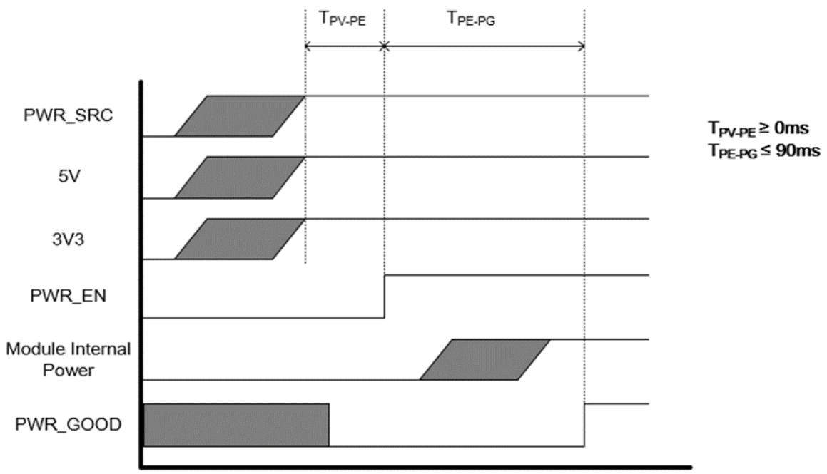
For initial power on, or to Resume from S3 and S4, this sequence must be followed.
![| Component           | Duration (ms) |\n|---------------------|---------------|\n| PWR_SRC             | 0             |\n| 5V                  | 0             |\n| 3V3                 | 0             |\n| PWR_EN              | 0             |\n| Module Internal Power | 90            |\n| PWR_GOOD            | 0             |](.egx-mxm-ada-series-50m-7c008-1000-10/f38af8c7847ca5d18503541d469ec1070b7316c5b0cac057d8eb238b065805e4.jpg)

Figure 13: Power sequencing

# Module Power Up and Down

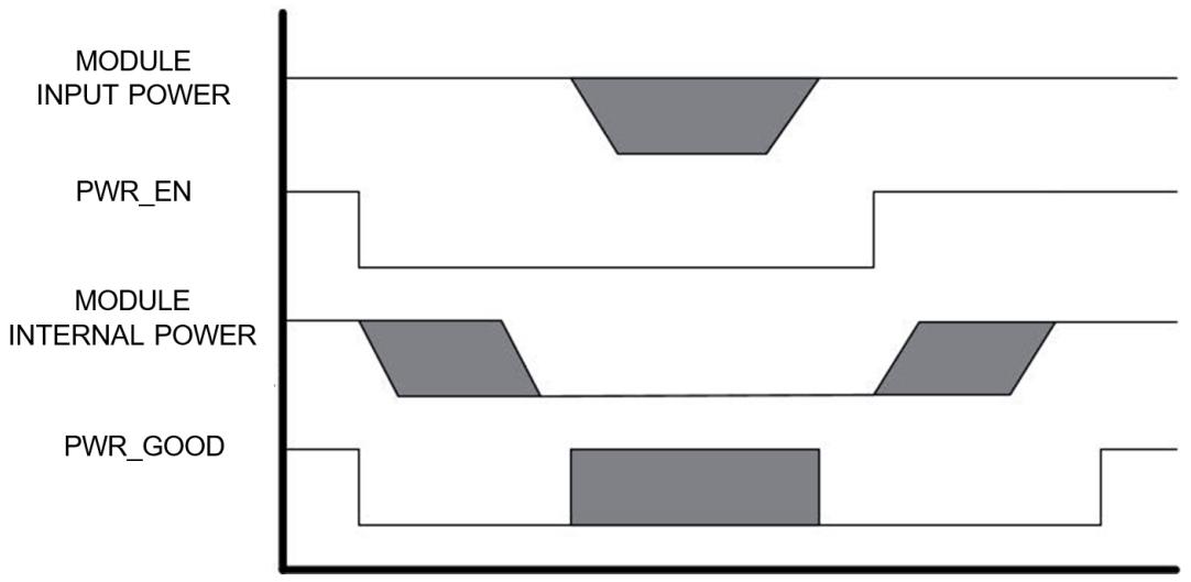
Issuing the PWR\_EN signal powers the MXM module down, and the system designer can decide whether to keep the module input power when the MXM module is powered down.
![| Signal Type           | Value |\n|-----------------------|-------|\n| INPUT POWER           | High  |\n| PWR_EN                | Low   |\n| MODULE INTERNAL POWER | Medium|\n| PWR_GOOD              | High  |](.egx-mxm-ada-series-50m-7c008-1000-10/ec9e91663e882d604145a1a78dceb2606487ec7f5a6cff72353d29164dbce649.jpg)

Figure 14: Modular power up and down

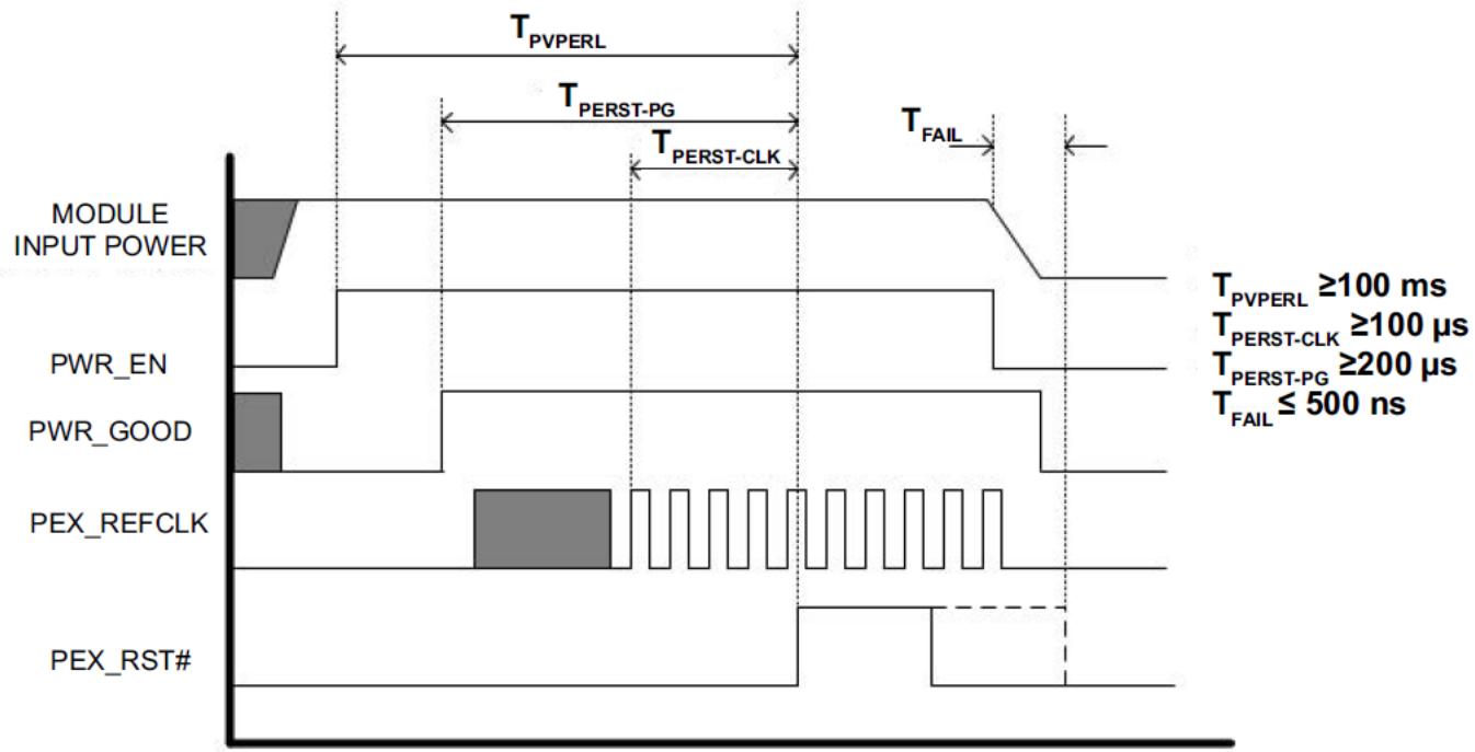
Reset Requirements
![| Signal          | Time Interval         |\n|-----------------|------------------------|\n| T_PVPERL        | ≥100 ms                |\n| T_PERST-CLK     | ≥100 µs                |\n| T_PERST-PG      | ≥200 µs                |\n| T_FAIL ≤ 500 ns | ≤ 500 ns               |](.egx-mxm-ada-series-50m-7c008-1000-10/5d12d9fd4472011ac0ed77af9608c06d620ed7af85d4e878528f39b7c9d22870.jpg)

Figure 15: Reset requirements

# Display Interface Configurations

# Dual Mode DisplayPort Implementation

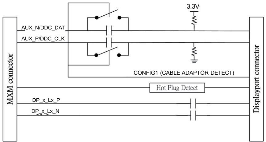
The EGX-MXM-AD2000/AD3500/AD5000 supports four dual mode DisplayPorts by default. HDMI can be supported via dongle. The system requires a switch circuit to determine whether the AUX or DDC signal is output from the MXM module, and AC coupling capacitors should be placed on the system board.
![Based on the provided block diagram, here is the accurate description of the blocks and connections:\n\n**Main Blocks:**\n*   **MXM connector**: A vertical rectangle on the left side.\n*   **Displayport connector**: A vertical rectangle on the right side.\n*   **CONFIG1 (CABLE ADAPTOR DETECT)**: A label situated below a switch block in the upper section.\n*   **Hot Plug Detect**: A rectangular block situated in the middle section.\n\n**Connections and Components:**\n*   **AUX_N/DDC_DAT** and **AUX_P/DDC_CLK**: These two lines connect the **MXM connector** to the **Displayport connector**. They pass through a block containing two switches and two capacitors (vertical parallel lines). The switches are drawn in parallel with the capacitors, allowing them to bypass the capacitors. This block is labeled **CONFIG1 (CABLE ADAPTOR DETECT)**.\n*   **3.3V**: Connected via a resistor to the **AUX_N/DDC_DAT** line (on the right side of the switch block).\n*   **Ground**: Connected via a resistor to the **AUX_P/DDC_CLK** line (on the right side of the switch block).\n*   **Hot Plug Detect**: Two unlabeled lines connect the **MXM connector** to the **Displayport connector** by passing through the **Hot Plug Detect** block.\n*   **DP_x_Lx_P** and **DP_x_Lx_N**: These two lines connect the **MXM connector** to the **Displayport connector**. They feature series capacitors (vertical parallel lines) near the **Displayport connector** end.](.egx-mxm-ada-series-50m-7c008-1000-10/14ba8c231393da42149108ddf54bf4e7bed1355d0cbfad33ff1702f9c4e6bd87.jpg)

Figure 16: Dual mode DisplayPort implementation

# HDMI on DisplayPort Interface

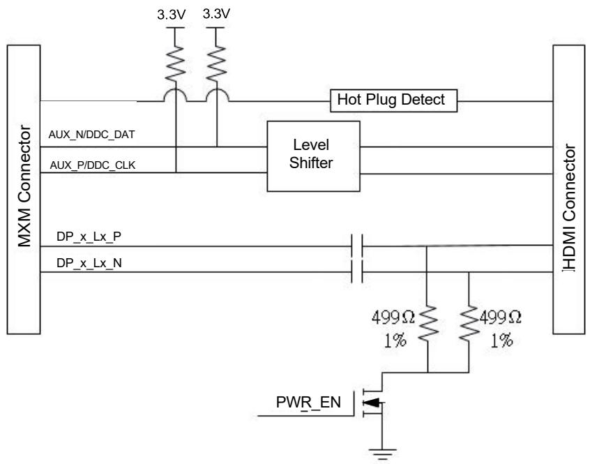
HDMI connectors can both be implemented through the DisplayPort interface. To support HDMI display from MXM, the HDMI port needs to be routed based on the Circuits required on the system board are as shown. 499Ω with 1% pulldown resistors to the ground on the DP lanes must place on the HDMI connector side of the AC coupling, gated by a MOSFET to limit leakage.
![3.3V 3.3V\nHot Plug Detect\nMXM Connector\nAUX_N/DDC_DAT\nAUX_P/DDC_CLK\nLevel Shifter\nHDMI Connector\nDP_x_Lx_P\nDP_x_Lx_N\n499Ω 499Ω\n1%\n1%\nPWR_EN](.egx-mxm-ada-series-50m-7c008-1000-10/8797712ab3c8630ebfc511b2bae08e69616aefcbaed354c97f250cdffff545ce.jpg)

Figure 17: HDMI on DisplayPort interface

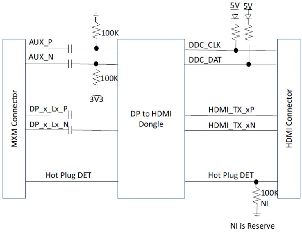
For resolutions higher than 1080p, contact an ADLINK FAE for customized service, or use an active IC in the circuit design.
![This is a block diagram for a **DP to HDMI Dongle** connecting an **MXM Connector** (left) to an **HDMI Connector** (right).\n\n**Connections from MXM Connector to DP to HDMI Dongle:**\n*   **AUX_P**: Connected via a capacitor. A **100K** resistor connects this line to Ground.\n*   **AUX_N**: Connected via a capacitor. A **100K** resistor connects this line to **3V3**.\n*   **DP_x_Lx_P**: Connected via a capacitor.\n*   **DP_x_Lx_N**: Connected via a capacitor.\n*   **Hot Plug DET**: Connected directly.\n\n**Connections from HDMI Connector to DP to HDMI Dongle:**\n*   **DDC_CLK**: Connected directly. It is pulled up to **5V** via a diode and a resistor.\n*   **DDC_DAT**: Connected directly. It is pulled up to **5V** via a diode and a resistor.\n*   **HDMI_TX_xP**: Connected directly.\n*   **HDMI_TX_xN**: Connected directly.\n*   **Hot Plug DET**: Connected directly. A **100K** resistor connects this line to Ground. The resistor is labeled **NI**. Below the resistor, text reads '**NI is Reserve**'.](.egx-mxm-ada-series-50m-7c008-1000-10/a7ce95690b583ab70b82b31a523d4c8a1b20ef37b789a3e49ea5347c407fa221.jpg)

Figure 18: HDMI on DisplayPort interface (For resolutions higher than 1080p)

# Driver Installation

Drivers can be downloaded through the following links:

Ada 2000 Driver: https://www.adlinktech.com/Products/DownloadSoftwareDriver?lang=zhhant&pdNo=2173&MainCategory=embedded-graphics-solutions&kind=DR

Ada 3500 Driver: https://www.adlinktech.com/Products/DownloadSoftwareDriver?lang=zhhant&pdNo=2243&MainCategory=embedded-graphics-solutions&kind=DR

Ada 5000 Driver:

https://www.adlinktech.com/Products/DownloadSoftwareDriver?lang=en&pdNo=2244&MainCategory=embeddedgraphics-solutions&kind=DR

# System BIOS Settings

The system BIOS must meet the following criteria:

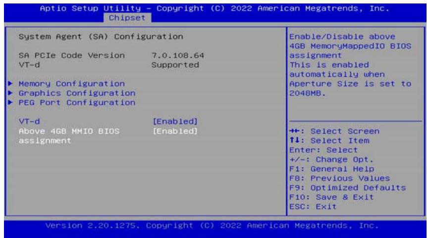
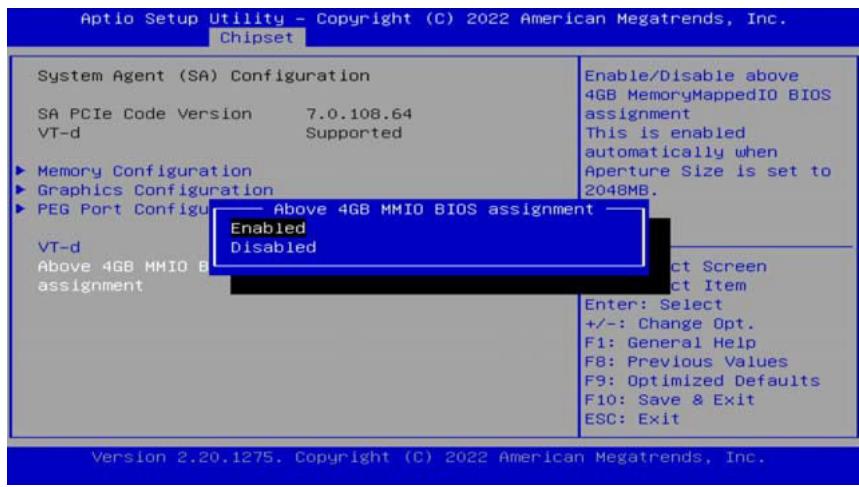
 SBIOS must support the "Above 4G decoding" feature to support a resizable BAR1 size.
 SBIOS must enable "Above 4G decoding" as the default configuration.

The following is a sample BIOS menu setting for reference. The actual menu setting can vary depending on the specific SBIOS design.
![Aptio Setup Utility - Copyright (C) 2022 American Megatrends, Inc.\nChipset\nSystem Agent (SA) Configuration\nSA PCIe Code Version 7.0.108.64\nVT-d Supported\n► Memory Configuration\n► Graphics Configuration\n► PEG Port Configuration\nVT-d (Enabled)\nAbove 4GB MMIO BIOS (Enabled)\nassignment\nEnable/Disable above\n4GB MemoryMappedIO BIOS\nassignment\nThis is enabled\nautomatically when\nAperture Size is set to\n2048MB.\n++: Select Screen\n↑↓: Select Item\nEnter: Select\n+/-: Change Opt.\nF1: General Help\nF8: Previous Values\nF9: Optimized Defaults\nF10: Save & Exit\nESC: Exit\nVersion 2.20.1275. Copyright (C) 2022 American Megatrends, Inc.](.egx-mxm-ada-series-50m-7c008-1000-10/bf0676079ecb2a2fa6d24de4ecd56ad4fc04cc01e21dc3692f64b33f2fac9b81.jpg)

![Aptio Setup Utility - Copyright (C) 2022 American Megatrends, Inc.\nChipset\nSystem Agent (SA) Configuration\nSA PCIe Code Version 7.0.108.64\nVT-d Supported\n► Memory Configuration\n► Graphics Configuration\n► PEG Port Configu Above 4GB MMIO BIOS assignment —\nVT-d\nAbove 4GB MMIO B assignment\nEnabled\nDisabled\nEnter: Select\n+/-: Change Opt.\nF1: General Help\nF8: Previous Values\nF9: Optimized Defaults\nF10: Save & Exit\nESC: Exit\nVersion 2.20.1275. Copyright (C) 2022 American Megatrends, Inc.](.egx-mxm-ada-series-50m-7c008-1000-10/1d7acbb14409a3299ede56c22c2d6e820362e456cf3c978dd0bb241bc4f3a080.jpg)

# Safety Instructions

Read and follow all instructions marked on the product and in the documentation before you operate your system. Retain all safety and operating instructions for future use.

• Please read these safety instructions carefully.
• Please keep this User‘s Manual for later reference.
• Read the specifications section of this manual for detailed information on the operating environment of this equipment.
• When installing/mounting or uninstalling/removing equipment, turn off the power and unplug any power cords/cables.
• To avoid electrical shock and/or damage to equipment:

 Keep equipment away from water or liquid sources.
 Keep equipment away from high heat or high humidity.
 Keep equipment properly ventilated (do not block or cover ventilation openings).
 Make sure to use recommended voltage and power source settings.
 Always install and operate equipment near an easily accessible electrical socket-outlet.
 Secure the power cord (do not place any object on/over the power cord).
 Only install/attach and operate equipment on stable surfaces and/or recommended mountings.
 If the equipment will not be used for long periods of time, turn off and unplug the equipment from its power source.

• Never attempt to fix the equipment. Equipment should only be serviced by qualified personnel.

# Getting Services

Ask an Expert: https://www.adlinktech.com/en/Askanexpert

# ADLINK Technology, Inc.

<table><tr><td>Address:</td><td>No. 66, Huaya 1st Road, Guishan DistrictTaoyuan City 333, Taiwan</td></tr><tr><td>Tel:</td><td>+886-3-216-5088</td></tr><tr><td>Fax:</td><td>+886-3-328-5723</td></tr><tr><td>Email:</td><td>service@adlinktech.com</td></tr></table>

# Ampro ADLINK Technology, Inc.

Address: 6450 Via Del Oro, San Jose, CA 95119-1208, USA

Tel: +1-408-360-0200

Toll Free: +1-800-966-5200 (USA only)

Fax: +1-408-600-1189

Email: info@adlinktech.com

# ADLINK Technology (China) Co., Ltd.

<table><tr><td>Address:</td><td>300 Fang Chun Rd., Zhangjiang Hi-Tech Park, Pudong New Area Shanghai, 201203 China</td></tr><tr><td>Tel:</td><td>+86-21-5132-8988</td></tr><tr><td>Fax:</td><td>+86-21-5132-3588</td></tr><tr><td>Email:</td><td>market@adlinktech.com</td></tr></table>

# ADLINK Technology GmbH

<table><tr><td>Address:</td><td>Hans-Thoma-Strasse 8-10, 68163 Mannheim, Germany</td></tr><tr><td>Tel:</td><td>+49-621-43214-0</td></tr><tr><td>Fax:</td><td>+49-621 43214-30</td></tr><tr><td>Email:</td><td>emea@adlinktech.com</td></tr></table>

Please visit the Contact page at www.adlinktech.com for information on how to contact the ADLINK regional office nearest you.
[🔗 Link to the original document](.egx-mxm-ada-series-50m-7c008-1000-10/egx-mxm-ada-series-50m-7c008-1000-10.pdf)
