#

# ETX-AT

# User’s Manual

![Green printed circuit board with various electronic components and connectors (no readable text or symbols)](.etx-at-50-1j020-1020-202/088598a727d84c5b479c8d5e5e8e5324475cddc7caf7975cbac3294ef249ae21.jpg)

Manual Revision: 2.02

Revision Date: October 27, 2009

Part Number: 50-1J020-1020

Revision History

<table><tr><td>Revision</td><td>Date</td><td>Change(s)</td></tr><tr><td>2.00</td><td>2009/05/18</td><td>Initial Release</td></tr><tr><td>2.01</td><td>2009/08/05</td><td>Correct LAN specification, remove SSD support, add SSDDR support</td></tr><tr><td>2.02</td><td>2009/10/27</td><td>Change SSDDR support to BOM option, update Ordering Information, Block Diagram</td></tr></table>

# Table of Contents

# Preface . 5

# 1 Introduction..

1.1 Description ...

# 2 Specifications .. 8

2.1 General .. 8

2.2 Integrated Video ..... 8

2.3 Audio ... 9

2.4 LAN .. 9

2.5 Multi I/O 9

2.6 Super I/O . 9

2.7 TPM (Trusted Platform Module) . 9

2.8 Power Specifications .... .. 10

2.9 Operating Systems Support .. . 11

2.10 Mechanical and Environmental . . 11

2.11 Ordering Information .. . 11

# 3 Function Diagram . 12

# 4 Mechanical Dimensions . . 13

# 5 Embedded Functions . 1 4

5.1 Watchdog Timer ...... . 14

5.2 Hardware Monitoring.. . 15

# 6 Pin-out and Signal Descriptions . 16

6.1 Connector Locations . . 16

6.2 Pin Compatibility .. . 16

6.3 Pin Definitions . . 17

6.4 Signal Descriptions . . 22

# 7 System Resources.. . 31

7.1 System Memory Map ....... .. 31

7.2 Direct Memory Access Channels . . 31

7.3 I/O Address Map ...... . 32

7.4 Interrupt Request (IRQ) Lines . . 34

7.5 PCI Configuration Space Map. . 35

7.6 PCI Interrupt Routing Map .. . 36
7.7 System Management Bus (I2C-compatible).. . 36

# 8 BIOS Setup Utility .. . 37

8.1 Starting the BIOS . . 37
8.2 Main Setup .. . 41
8.3 Advanced BIOS Setup . . 42
8.4 Power Management . . 60
8.5 Boot Setup . . 64
8.6 Security Setup. . 68
8.7 Exit Menu .. .. 71

# 9 BIOS Checkpoints, Beep Codes.. . 73

9.1 Bootblock Initialization Code Checkpoints . . 74
9.2 Bootblock Recovery Code Checkpoints .... . 75
9.3 POST Code Checkpoints . 76
9.4 OEM POST Error Checkpoints . 78
9.5 DIM Code Checkpoints . . 78
9.6 ACPI Runtime Checkpoints. . 79
9.7 Boot Block Beep Codes .... . 80
9.8 POST BIOS Beep Codes . . 80
9.9 Troubleshooting POST BIOS Beep Codes . 81

# Appendix A: Connectors and Mounting . . 82

A.1 Carrier Board ETX Connecter Heights (Hirose FX8/FX8C Receptacles) . .. 82
A.3 Mounting Procedures . . 83
A.4 Standoff Types - Carrier Board . 84

# Appendix B: Heatspreaders and Heatsinks .. . 85

B.1 Heatspreader Introduction.. . 85
B.2 Heatspreader Dimensions for HTS-EAT-B (threaded type) . . 86
B.3 Heatspreader Dimensions for HTS-EAT-BT (through-hole type) .. . 87
B.4 Heatsinks: THS-EAT-B and THSH-EAT-BL (threaded type) . . 88
B.5 Dimensions for THS-EAT-B Heatsink . . 90
B.6 Dimensions for THSH-EAT-BL Heatsink . . 91

# Important Safety Instructions . . 92

# Getting Service . . 94

# Preface

# Copyright 2009 ADLINK Technology, Inc.

This document contains proprietary information protected by copyright. All rights are reserved. No part of this manual may be reproduced by any mechanical, electronic, or other means in any form without prior written permission of the manufacturer.

# Disclaimer

The information in this document is subject to change without prior notice in order to improve reliability, design, and function and does not represent a commitment on the part of the manufacturer.

In no event will the manufacturer be liable for direct, indirect, special, incidental, or consequential damages arising out of the use or inability to use the product or documentation, even if advised of the possibility of such damages.

# Environmental Responsibility

ADLINK is committed to fulfill its social responsibility to global environmental preservation through compliance with the European Union's Restriction of Hazardous Substances (RoHS) directive and Waste Electrical and Electronic Equipment (WEEE) directive. Environmental protection is a top priority for ADLINK. We have enforced measures to ensure that our products, manufacturing processes, components, and raw materials have as little impact on the environment as possible. When products are at their end of life, our customers are encouraged to dispose of them in accordance with the product disposal and/or recovery programs prescribed by their nation or company.

# Trademarks

AMIBIOS®8 is a registered trademark of American Megatrends, Inc. ETX® is a registered trademark of Kontron Embedded Modules GmbH.

Product names mentioned herein are used for identification purposes only and may be trademarks and/or registered trademarks of their respective companies.

# Conventions

Take note of the following conventions used throughout this manual to make sure that users perform certain tasks and instructions properly.

![The image displays a small icon featuring a white document with horizontal lines, overlaid with a large red checkmark. Below the document, the text 'NOTE:' is written in black capital letters.](.etx-at-50-1j020-1020-202/b05d20bdf5c936f5150d654231286c5422688bd2e7521de66fe6699cccbc3844.jpg)

Additional information, aids, and tips that help users perform tasks.

![This image features a standard yellow triangular warning sign with a black border. Inside the triangle is a large black exclamation point. Below the triangle, the text 'CAUTION:' is printed in black capital letters.](.etx-at-50-1j020-1020-202/2e6efd977e97a01f92f570334aa7a1daee75d560fe0de2d2b91380ee46971d92.jpg)

Information to prevent minor physical injury, component damage, data loss, and/or program corruption when trying to complete a task.

![The image displays a warning sign consisting of a red triangle pointing upward with a white exclamation point centered inside it. Below the triangle, the word 'WARNING:' is printed in black capital letters.](.etx-at-50-1j020-1020-202/df15e1f8228e56a04d22bf4d34f77ed5752a55a309a0e0f7a585e745a5d30dbe.jpg)

Information to prevent serious physical injury, component damage, data loss, and/or program corruption when trying to complete a specific task.

# 1 Introduction

# 1.1 Description

The ETX-AT is an ETX v3.02 compliant module specially designed to facilitate speedy development of semi custom designs. ETX is an open standard that targets the market for embedded OEM projects. An ETX core combined with a custom made carrier board represents a value solution that allows OEM customers to get to the market fast. The new ETX v3.02 specification adds SATA support to ETX in the form of two connectors on the module itself, leaving the ETX board-to-board interface 100% compatible with baseboards designed under the earlier ETX v2.xx specification.

The ETX-AT is positioned as an entry level ETX module for generic systems, but is also suitable for systems requiring a full set of graphics features. The module comes with integrated support for high resolution CRT, single/dual channel 18/24-bits LVDS, and TV out (SDTV and HDTV)

Built on Intel's 45nm process, the Intel® Atom™ processor N270 with 512 kByte L2 cache on the ETX-AT features a thermal design power of just 2.5 watts at peak levels while supporting Intel® SpeedStep® Technology. The Intel® Atom™ processor N270 also supports Hyper Threading Technology, essentially giving it the performance of a dual core processor. Its thermal design and powerful CPU core allows the ETX-AT to provide the same or even better performance than earlier generation modules at more modest power consumption.

![The image displays the Intel Atom logo, featuring a rounded rectangular badge. The top section is white and contains the blue 'intel' logo enclosed in a ring. The bottom section has a blue gradient background and features the word 'Atom' in large blue letters, with the word 'inside' in smaller white text directly beneath it.](.etx-at-50-1j020-1020-202/f3c716ddcba7e65e8b084b0286e5afef56431b1c552dfba701ccff8860d12659.jpg)

In addition to two SATA ports, the module offers dual channel EIDE supporting both PIO and UDMA modes, four USB ports, two serial ports, one parallel port (SPP/ECP/EPP) shared with FDD, one PS2 keyboard/mouse interface and power management functionality. Additionally onboard is an 10/100Base-T Ethernet port, and an HD Audio Codec.

The ETX-AT fully supports PCI and legacy ISA based on high speed PCI/ISA bridge. The module comes equipped with AMIBIOS®8 supporting embedded features such as: Remote Console, CMOS backup for battery-less operation, CPU and System Monitoring, and a Watchdog Timer.

The ETX-AT has been designed and verified for use with Virtium's SSDDR SODIMM dual function memory modules, while maintaining full backwards compatibility with standard SODIMM memory. Virtium’s SSDDR combines a NAND Flash Serial ATA Solid State Drive (SATA SSD) and DDR2 memory on a single SODIMM module by utilizing reserved pins on the SODIMM for SATA interface signal transfer, thereby remaining fully JEDEC compatible.

The ETX-AT is available with native Intel single channel 18-bit LVDS support or with single/dual channel 18/24-bit LVDS based on the Chrontel CH7308B connected via SDVO.

![ADLINK\nGREEN\nRoHS Compliant](.etx-at-50-1j020-1020-202/2c22415fb384f57874ddda8099b040ec352c509774a6dfa944c7c0af4091bfdb.jpg)

The ETX-AT is a RoHS compliant and leadfree product.

# 2 Specifications

# 2.1 General

f CPU: Intel® Atom™ N270, FSB 533, 1.6 GHz with 512 KB L2 cache,
2.5 W, on-die primary 32-kB instructions cache and
- 24-kB write-back data cache
- 2-thread support
- Advanced gunning transceiver logic (AGTL+) bus driver technology
- Enhanced Intel® SpeedStep® Technology
- Source synchronous double-pumped (2x) Address
- Source synchronous quad-pumped (4x) Data
- C0\~C4 low power states supported

f Memory: Single SODIMM socket supporting: - up to 2 GB of non-ECC, un-buffered, 533 MHz standard DDR2 SODIMM memory - Virtium SSDDR type module combining NAND flash SATA Solid State Drive and DDR2 memory on a single SODIMM module (ETX-AT-N270-SD/18SD only)

f Chipset: Intel® 945GSE Express Graphic Memory Controller Hub and Intel® I/O Controller Hub 7 Mobile (ICH7M)

f BIOS: AMIBIOS®8 with CMOS backup in 8 Mbit SPI BIOS

f Hardware Monitor:Supply voltages and CPU temperature

f Watchdog Timer: Programmable timer ranges to generate RESET

f Expansion Busses: 32-bit PCI 2.3 Masters at 33 MHz ISA 16-bit SMBus/I2C

# 2.2 Integrated Video

f Chipset: Intel® Graphics Media Accelerator 950 integrated into 945GSE GMCH supporting dual independent display
f CRT Interface: Analog CRT support up to 2048 x1536 resolution @ 70Hz (QXGA)
f LVDS Interface:
- single channel 18-bit TFT with resolution up to 1280x1024 (ETX-AT-N270-18)
- single/dual channel 18/24-bit TFT with resolution up to 1600x1200 (ETX-AT-N270)
f TV-out: NTSC/PAL, SDTV, HDTV 480p/720p/1080i/1080p modes supported (without Macrovision)

# 2.3 Audio

f Chipset: Integrated in Intel® I/O Controller Hub 7 Mobile (ICH7M)
f Audio Codec: AC’97 or HDA type on carrier

# 2.4 LAN

f Chipset: ICH7M integrated MAC with Intel® 82562 PHY
f Interface: 10/100 Mbps with Wake-on-LAN and Alert on LAN support

# 2.5 Multi I/O

f IDE (PATA): Two channels IDE with UDMA 100 support
f SATA: Two channels SATA-150 (ETX-AT-N270-SD/18SD support 1 channel only)
f USB: Supports up to eight ports USB v.2.0

# 2.6 Super I/O

f Chipset: W83627HG
f Serial: Two high speed RS-232C ports (COM1/COM2)
f IrDA: SIR IrDA 1.1 compliant
f Parallel: SPP, EPP, and ECP mode (pin out shared with FDD)
f FDD: One drive (pin out shared with LPT)
f Keyboard & Mouse: One PS/2 keyboard and one PS/2 mouse

# 2.7 TPM (Trusted Platform Module)

f Chipset: Infineon SLB9635TT1.2
f Type: TPM 1.2

# 2.8 Power Specifications

f Input Power: AT mode and ATX mode
f Power Management: ACPI 3.0 compliant with battery support
f Power States: supports S0, S1, S3, S4, S5

![Yellow lightning bolt symbol on white background (no text or symbols)](.etx-at-50-1j020-1020-202/f2ccb0e2ba9b70e3cfe959f2dfc6755384f9d85abe478c5474d3bcc016bf6267.jpg)

Test Configuration

<table><tr><td>Function</td><td>Configuration</td></tr><tr><td>CPU</td><td>Intel® AtomTM Processor N270, 512MB L2, 533MHz, 45nm, 1.6GHz</td></tr><tr><td>Memory</td><td>Apacer PC2-4300 CL4 512MB</td></tr><tr><td>Graphics</td><td>945GSE</td></tr><tr><td>SATA Channel</td><td>Seagate Barracuda 7200.10 160BG</td></tr><tr><td>Backplane</td><td>ETX-Proto</td></tr><tr><td>Power Supply</td><td>LEMACS HG2-6350P 350W</td></tr></table>

Intel® Atom™ N270, 1.6 GHz

<table><tr><td>Power State</td><td>Power Requirement</td><td>Current</td><td>Power</td></tr><tr><td>DOS (idle)</td><td>+5V</td><td>2.26A</td><td>11.3W</td></tr><tr><td>Linux (idle)</td><td>+5V</td><td>2.15A</td><td>10.75W</td></tr><tr><td>Windows XP logon screen (idle)</td><td>+5V</td><td>2.25A</td><td>11.25W</td></tr><tr><td>Windows XP CPU Stress (Kpower)</td><td>+5V</td><td>2.54A</td><td>12.7W</td></tr><tr><td>Windows XP Total System Stress (Burnin)</td><td>+5V</td><td>2.48A</td><td>12.4W</td></tr><tr><td>S5 Mode (soft off)</td><td>5V Standby</td><td>131.6mA</td><td>0.658W</td></tr><tr><td>S4 Mode (hibernate)</td><td>5V Standby</td><td>65.6mA</td><td>0.328W</td></tr><tr><td>S3 Mode (suspend to RAM)</td><td>5V Standby</td><td>79.1mA</td><td>0.396W</td></tr></table>

CMOS Battery Power Consumption

<table><tr><td>Current (+3V)</td><td>Power</td></tr><tr><td>2.6 μA</td><td>0.0000078 W</td></tr></table>

# 2.9 Operating Systems Support

f Standard Support

\- Windows XP 32-bit

\- Windows Vista 32-bit

\- Linux 2.6.x

f Extended Support (BSP)

\- Embedded XP BSP

\- WinCE 6.0 BSP

\- Linux 2.6.x BSP

f Libraries, API support

\- AIDI I2C Library for Win32, WinCE and Linux

# 2.10 Mechanical and Environmental

f Form factor and Type: ETX rev 3.02

f Dimensions: 95 x 114 mm

f Standard Operating Temperature: $0 ^ { \circ } \complement$ to $6 0 ^ { \circ } \complement$

f Relative Humidity: 5% to 95%

f Shock : 15G peak-to-peak, 11ms duration, non-operation

f Vibration:

Non-operating : 1.88 Grms, 5-500 Hz, each axis

Operating : 0.5 Grms, 5-500 Hz, each axis

f Certification : CE, FCC

# 2.11 Ordering Information

f ETX-AT-N270

ETX Module with Intel® Atom™ processor N270 and 945GSE / ICH7M chipset and support for single/dual channel 24-bit LVDS

f ETX-AT-N270-18

ETX Module with Intel® Atom™ processor N270 and 945GSE / ICH7M chipset and support for single channel 18-bit LVDS

f ETX-AT-N270-SD / ETX-AT-N270-18SD

ETX Module with Intel® Atom™ processor N270 and 945GSE / ICH7M chipset with 24-bit integrated LVDS and SSDDR support (“18SD” supports 18-bit LVDS)

# 3 Function Diagram

![**Labeled Blocks:**\n\n*   **CPU:** CPU Atom N270 Micro-FCBGA\n*   **Northbridge:** Northbridge Intel® 945GSE (containing PCIe VGA, SDTV HDTV, SDVO_B, Graphic Core 250 Mhz, DDR2 Memory Controller)\n*   **Southbridge:** Southbridge Intel® ICH7M (containing Ethernet MAC, IDE PATA, PCI Express x1, SATA, RTC, SPI, LPC, PCI Controller, Audio, USB 2.0)\n*   **Memory/Storage:** SODIMM DDR2 533 Mhz, optional SSDDR DDR2 + SSD, SATA (two blocks), PATA IDE0/IDE1\n*   **Video/Display:** LAN PHY Intel 82562EZ, CRT, TV-out, LVDS Single/dual 18/24-bit CH7308B\n*   **Interfaces/Controllers:** PCIe to PATA JML368, PCI / ISA IT8888G, SMBus, I2C, BC, PCI Bus\n*   **System Management:** BIOS, Super I/O Winbond W83627HG, TPM, Debug header\n*   **Peripherals:** Keyboard, Mouse, LPT1/FDD, COM1, COM2\n*   **Audio/USB:** Audio Codec Realtek ALC268, Four port USB 2.0\n*   **External Connectors:** X1, X2, X3, X4\n\n**Connections:**\n\n*   **CPU Atom N270 Micro-FCBGA** connects bidirectionally to **Northbridge Intel® 945GSE**.\n*   **Northbridge Intel® 945GSE** connects bidirectionally to **Southbridge Intel® ICH7M**.\n*   **Northbridge** connects to:\n    *   **LAN PHY Intel 82562EZ**\n    *   **PATA IDE0/IDE1**\n    *   **CRT**\n    *   **TV-out**\n    *   **LVDS Single/dual 18/24-bit CH7308B**\n    *   **SODIMM DDR2 533 Mhz**\n    *   **optional SSDDR DDR2 + SSD** (dashed connection)\n    *   **PCI / ISA IT8888G**\n*   **Southbridge** connects to:\n    *   **PCIe to PATA JML368**\n    *   **BIOS** (via SPI)\n    *   **Super I/O Winbond W83627HG** (via LPC)\n    *   **PCI Bus**\n    *   **Audio Codec Realtek ALC268** (via Audio)\n    *   **Four port USB 2.0** (via USB 2.0)\n    *   **BC** (via SMBus and I2C)\n    *   **SATA** (via SATA)\n*   **Super I/O** connects to **TPM**, **Debug header**, **Keyboard**, **Mouse**, **LPT1/FDD**, **COM1**, and **COM2**.\n*   **X4** connects to **LAN PHY Intel 82562EZ**, **PATA IDE0/IDE1**, **CRT**, **TV-out**, and **LVDS Single/dual 18/24-bit CH7308B**.\n*   **X2** connects to **PCI / ISA IT8888G**.\n*   **X1** connects to **PCI Bus**, **Audio Codec Realtek ALC268**, and **Four port USB 2.0**.\n*   **X3** connects to the two **SATA** blocks, **BC**, **Keyboard**, **Mouse**, **LPT1/FDD**, **COM1**, and **COM2**.](.etx-at-50-1j020-1020-202/e0bc86088b611d8c416d85db6f5792255e2510498991a0de4513f52d3796b6b2.jpg)

# 4 Mechanical Dimensions

![SIDE VIEW\n2\n5,13\nX3\n41.7\nX4\n92.5\n95\n3\n0\n2.5\n0\n2.4\nØ5.5\nØ2.7\nTOP VIEW\nX1-X4 connectors\non bottom side\n61.95\n111.6\n114\nX1\n45.9\nX2\n111\n87.5](.etx-at-50-1j020-1020-202/9517a0dc88712b5a68651055bf001ffb1d7c62a28b716f2bfc2cc0ad4e12a832.jpg)

All tolerances ± 0.05 mm
Other tolerances ± 0.2 mm

# 5 Embedded Functions

All embedded board functions on ADLINK’s Computer on Modules are supported at the operating system level using the ADLINK Intelligent Device Interface (AIDI) library. The AIDI API programming interface is compatible and identical across all supported ADLINK Computer on Modules and all supported operating systems. The AIDI library includes a demo program to demonstrate the library’s functionallity.

# 5.1 Watchdog Timer

The ETX-AT implements a Watchdog timer that can be used to automatically detect software execution problems or system hangs and reset the board if necessary. The Watchdog timer consists of a counter that counts down from an initial value to zero. When the system is operating normally, the software that sets the intial value periodically resets the counter so that the it never reaches zero. If the counter reaches zero before the software resets it, the system is presumed to be malfunctioning and a reset signal is asserted.

![Cartoon illustration of a bulldog wearing a red collar (no text or symbols)](.etx-at-50-1j020-1020-202/dc38b574ae898cbfdc3ff11a688bc9a53cce996ff197fbdb2523278af31f653a.jpg)

The AIDI Library Watchdog functions support Watchdog control of the board. If the Watchdog begins countdown and reaches zero, it will access the CPU's RESET signal to reset the system. This application must call another function named AidiWDogTrigger that triggers the Watchdog to restart to prevent system reset.

AIDI Demo Program - Watchdog Tab

The AIDI Demo Program allows retrieval of the current Watchdog status and updating of the Watchdog settings

If the Watchdog is enabled, the user can click the WDT Trigger button to manually reset the counter and prevent the system from resetting

![AIDI DEMO Program\nBoard Info | StorageArea | I2C-Buses | HW-Monitor | GPIO | WatchDog |\nWatchDog Info\n1\nNumber 1 MinTimeout: 0 ms MaxTimeout: 255000 ms\nMinDelay: 0 ms MaxDelay: 255000 ms\nWatchDog Operation\nStart WatchDog\nTimeout(dec): ms\nDelay(dec): ms\nEnable Disable\nGetWatchDog Config\nTimeout(dec): ms\nDelay(dec): ms\nGetConfig\nWDT Trigger\nNote: the sum of timeout value and delay value can't exceed MaxTimeout or MaxDelay](.etx-at-50-1j020-1020-202/9a43b315ff80503ba4cc4fc49e54e78f9b3df4d30388480263dc856de7876e30.jpg)

# 5.2 Hardware Monitoring

To ensure system health of your embedded system ADLINK’s Computer on Modules come with built in support for monitoring of CPU temperatures and critical module voltage levels.

The AIDI Library provides simple APIs at the application level to support these functions and adds alarm functions when voltage or temperature levels exceeds the upper or lower limit set by the user.

On the ETX-AT the following monitored values can be read from the module:

CPU temperature, Vcore, 1.05V, 3.3V, 5V and VBAT.

AIDI Demo Program

\- HW Monitor Tab

Field 1 displays detected sensors (number).

Field 2 allows setting of upper and lower alarm limits.

Field 3 displays read out information of sensors.

![AIDI DEMO Program\nBoard Info | StorageArea | I2C-Buses | HW-Monitor | GPIO | WatchDog |\nSensor Info\n1\nTemperature  Pan  Voltage  Number:\nType:\nSensor Limit\n2\nUpper Alarm Threshold:  Lower Alarm Threshold:\nUpper Alarm Hysteresis  Lower Alarm Hysteresis:  GetLimit\nMaximum Value :  Minimum Value :  Unit:  SetLimit\nNote: Input decimal data, threshold value must higher than hysteresis value\nStatus\n3\nValue:    Unit\nStatus:        Get Data](.etx-at-50-1j020-1020-202/274cd614a2087f63dcbad4faf8857594c5e2177f200f449946a5e15b1575de2e.jpg)

# 6 Pin-out and Signal Descriptions

# 6.1 Connector Locations

![- Ethernet\n- IDE1/IDE2\n- Power Signals\n- Speaker, Battery\n- I²C & SMB bus\nX4\nETX-AT\n(top view)\n- ISA bus\nX2\nX3\n- VGA/LCD/Video\n- COM1/COM2\n- LPT1\n- IrDA\n- Mouse\n- Keyboard\nX1\n- 32-bit PCI bus\n- USB\n- Audio](.etx-at-50-1j020-1020-202/b22996e17a9463bf3af4afe8661c1d00a4fcce18e288acd94ee4acd547a36199.jpg)

# 6.2 Pin Compatibility

All pins on X1, X2, X3, and X4 of the ETX-AT comply with pin and signal descriptions used in the ETX Specification version 3.02. This document contains a description of pins, signal descriptions, and mechanical characteristics of the ETX form factor.

![The image displays a white document icon featuring a large red checkmark and horizontal lines. Below the icon is the text 'NOTE:' in black, capitalized letters.](.etx-at-50-1j020-1020-202/c187e12aae81accc3516f691fb74562a5bd21405c6e96b809d0473648b6d3c1f.jpg)

Compared to earlier ETX revisons (ETX rev 2.x)

ETX 3.02 revision adds “SATA connectors on the module” to the ETX specification and is further pin to pin compatible with earlier 2.x ETX revisions.

(X1, X2, X3, X4 pinout on rev 2.x equal those on revison 3.02)

# 6.3 Pin Definitions

X1: PCI-bus, USB, & Audio

X1

![The image displays a black-and-white line drawing of a rectangular object resembling a SIM card. It features a central rectangular cutout and vertical rows of dashed lines running along the left and right edges, representing electrical contacts. The corners are labeled with numbers: '99' at the top left, '100' at the top right, '1' at the bottom left, and '2' at the bottom right.](.etx-at-50-1j020-1020-202/160033651a52412217662e2eb98d6a767c20f118ac29a862ac47bf1050e48e30.jpg)

<table><tr><td>Pin</td><td>Signal</td><td>Pin</td><td>Signal</td></tr><tr><td>1</td><td>GND</td><td>2</td><td>GND</td></tr><tr><td>3</td><td>PCICLK3</td><td>4</td><td>PCICLK4</td></tr><tr><td>5</td><td>GND</td><td>6</td><td>GND</td></tr><tr><td>7</td><td>PCICLK1</td><td>8</td><td>PCICLK2</td></tr><tr><td>9</td><td>REQ3#</td><td>10</td><td>GNT3#</td></tr><tr><td>11</td><td>GNT2#</td><td>12</td><td> $3V^1$ </td></tr><tr><td>13</td><td>REQ2#</td><td>14</td><td>GNT1#</td></tr><tr><td>15</td><td>REQ1#</td><td>16</td><td> $3V^1$ </td></tr><tr><td>17</td><td>GNT0#</td><td>18</td><td>RSV</td></tr><tr><td>19</td><td>5VCC</td><td>20</td><td>5VCC</td></tr><tr><td>21</td><td>SERIRQ</td><td>22</td><td>REQ0#</td></tr><tr><td>23</td><td>AD0</td><td>24</td><td> $3V^1$ </td></tr><tr><td>25</td><td>AD1</td><td>26</td><td>AD2</td></tr><tr><td>27</td><td>AD4</td><td>28</td><td>AD3</td></tr><tr><td>29</td><td>AD6</td><td>30</td><td>AD5</td></tr><tr><td>31</td><td>CBE0#</td><td>32</td><td>AD7</td></tr><tr><td>33</td><td>AD8</td><td>34</td><td>AD9</td></tr><tr><td>35</td><td>GND</td><td>36</td><td>GND</td></tr><tr><td>37</td><td>AD10</td><td>38</td><td>AUXAL</td></tr><tr><td>39</td><td>AD11</td><td>40</td><td>MIC</td></tr><tr><td>41</td><td>AD12</td><td>42</td><td>AUXAR</td></tr><tr><td>43</td><td>AD13</td><td>44</td><td>ASVCC</td></tr><tr><td>45</td><td>AD14</td><td>46</td><td>SDNL</td></tr><tr><td>47</td><td>AD15</td><td>48</td><td>ASSGND</td></tr><tr><td>49</td><td>CBE1#</td><td>50</td><td>SNDR</td></tr></table>

<table><tr><td>Pin</td><td>Signal</td><td>Pin</td><td>Signal</td></tr><tr><td>51</td><td>5VCC</td><td>52</td><td>5VCC</td></tr><tr><td>53</td><td>PAR</td><td>54</td><td>SERR#</td></tr><tr><td>55</td><td>GPERR</td><td>56</td><td>RSV</td></tr><tr><td>57</td><td>PME#</td><td>58</td><td>USB2-</td></tr><tr><td>59</td><td>LOCK#</td><td>60</td><td>DEVSEL#</td></tr><tr><td>61</td><td>TRDY#</td><td>62</td><td>USB3-</td></tr><tr><td>63</td><td>IRDY#</td><td>64</td><td>STOP#</td></tr><tr><td>65</td><td>FRAME#</td><td>66</td><td>USB2+</td></tr><tr><td>67</td><td>GND</td><td>68</td><td>GND</td></tr><tr><td>69</td><td>AD16</td><td>70</td><td>CBE2#</td></tr><tr><td>71</td><td>AD17</td><td>72</td><td>USB3+</td></tr><tr><td>73</td><td>AD19</td><td>74</td><td>AD18</td></tr><tr><td>75</td><td>AD20</td><td>76</td><td>USB0N</td></tr><tr><td>77</td><td>AD22</td><td>78</td><td>AD21</td></tr><tr><td>79</td><td>AD23</td><td>80</td><td>USB1-</td></tr><tr><td>81</td><td>AD24</td><td>82</td><td>CBE3#</td></tr><tr><td>83</td><td>5VCC</td><td>84</td><td>5VCC</td></tr><tr><td>85</td><td>AD25</td><td>86</td><td>AD26</td></tr><tr><td>87</td><td>AD28</td><td>88</td><td>USB0+</td></tr><tr><td>89</td><td>AD27</td><td>90</td><td>AD29</td></tr><tr><td>91</td><td>AD30</td><td>92</td><td>USB1+</td></tr><tr><td>93</td><td>PCIRST#</td><td>94</td><td>AD31</td></tr><tr><td>95</td><td>INTC#</td><td>96</td><td>INTD#</td></tr><tr><td>97</td><td>INTA#</td><td>98</td><td>INTB#</td></tr><tr><td>99</td><td>GND</td><td>100</td><td>GND</td></tr></table>

![The image displays an icon of a white piece of paper with faint horizontal lines, featuring a large red checkmark in the center. Below the paper graphic, the word 'NOTE:' is written in black, uppercase letters.](.etx-at-50-1j020-1020-202/8a881153539bd3c3ed1bd2d90888d1317991d46f862d2a18ebc1361126093732.jpg)

The 3V (3.3 V ±5%) is generated onboard. Pins may be used to power devices on the carrier board up to a maximum load of 500 mA.

![A yellow triangular warning sign with a black border containing a black exclamation point in the center. Below the triangle, the word 'CAUTION' is written in black capital letters.](.etx-at-50-1j020-1020-202/e2c901006d8f13b4e69afa6639543f669b5416f9f48918081dfc925047af4924.jpg)

Do not connect the 3V pin to external 3.3V supply power.

X2: ISA Bus

X2

![The image displays a vertical measuring scale or ruler. It features a central white rectangular body with small notches at the top and bottom centers. Flanking this central body are two columns of dense, fine horizontal tick marks running along the entire length. Numerical labels are positioned at the four corners: '99' at the top left, '100' at the top right, '1' at the bottom left, and '2' at the bottom right.](.etx-at-50-1j020-1020-202/2eadb7858430e3ac960330962b461e54c31a00b60ce51e07fcb7c7dc46f54883.jpg)

<table><tr><td>Pin</td><td>Signal</td><td>Pin</td><td>Signal</td></tr><tr><td>1</td><td>GND</td><td>2</td><td>GND</td></tr><tr><td>3</td><td>SD14</td><td>4</td><td>SD15</td></tr><tr><td>5</td><td>SD13</td><td>6</td><td>MASTER#</td></tr><tr><td>7</td><td>SD12</td><td>8</td><td>DREQ7</td></tr><tr><td>9</td><td>SD11</td><td>10</td><td>DACK7#</td></tr><tr><td>11</td><td>SD10</td><td>12</td><td>DREQ6</td></tr><tr><td>13</td><td>SD9</td><td>14</td><td>DACK6#</td></tr><tr><td>15</td><td>SD8</td><td>16</td><td>DREQ5</td></tr><tr><td>17</td><td>MEMW#</td><td>18</td><td>DACK5#</td></tr><tr><td>19</td><td>MEMR#</td><td>20</td><td>DREQ0</td></tr><tr><td>21</td><td>LA17</td><td>22</td><td>DACK0#</td></tr><tr><td>23</td><td>LA18</td><td>24</td><td>IRQ14</td></tr><tr><td>25</td><td>LA19</td><td>26</td><td>IRQ15</td></tr><tr><td>27</td><td>LA20</td><td>28</td><td> $IRQ12^1$ </td></tr><tr><td>29</td><td>LA21</td><td>30</td><td>IRQ11</td></tr><tr><td>31</td><td>LA22</td><td>32</td><td>IRQ10</td></tr><tr><td>33</td><td>LA23</td><td>34</td><td>IO16#</td></tr><tr><td>35</td><td>GND</td><td>36</td><td>GND</td></tr><tr><td>37</td><td>SBHE#</td><td>38</td><td>M16#</td></tr><tr><td>39</td><td>SA0</td><td>40</td><td>OSC</td></tr><tr><td>41</td><td>SA1</td><td>42</td><td>BALE</td></tr><tr><td>43</td><td>SA2</td><td>44</td><td>TC</td></tr><tr><td>45</td><td>SA3</td><td>46</td><td>DACK2#</td></tr><tr><td>47</td><td>SA4</td><td>48</td><td>IRQ3</td></tr><tr><td>49</td><td>SA5</td><td>50</td><td>IRQ4</td></tr></table>

<table><tr><td>Pin</td><td>Signal</td><td>Pin</td><td>Signal</td></tr><tr><td>51</td><td>5VCC</td><td>52</td><td>5VCC</td></tr><tr><td>53</td><td>SA6</td><td>54</td><td>IRQ5</td></tr><tr><td>55</td><td>SA7</td><td>56</td><td>IRQ6</td></tr><tr><td>57</td><td>SA8</td><td>58</td><td>IRQ7</td></tr><tr><td>59</td><td>SA9</td><td>60</td><td>SYSCLK</td></tr><tr><td>61</td><td>SA10</td><td>62</td><td>REFSH#</td></tr><tr><td>63</td><td>SA11</td><td>64</td><td>DREQ1</td></tr><tr><td>65</td><td>SA12</td><td>66</td><td>DACK1#</td></tr><tr><td>67</td><td>GND</td><td>68</td><td>GND</td></tr><tr><td>69</td><td>SA13</td><td>70</td><td>DREQ3</td></tr><tr><td>71</td><td>SA14</td><td>72</td><td>DACK3#</td></tr><tr><td>73</td><td>SA15</td><td>74</td><td>IOR#</td></tr><tr><td>75</td><td>SA16</td><td>76</td><td>IOW#</td></tr><tr><td>77</td><td>SA18</td><td>78</td><td>SA17</td></tr><tr><td>79</td><td>SA19</td><td>80</td><td>SMEMR#</td></tr><tr><td>81</td><td>IOCHRDY</td><td>82</td><td>AEN</td></tr><tr><td>83</td><td>5VCC</td><td>84</td><td>5VCC</td></tr><tr><td>85</td><td>SD0</td><td>86</td><td>SMEMW#</td></tr><tr><td>87</td><td>SD2</td><td>88</td><td>SD1</td></tr><tr><td>89</td><td>SD3</td><td>90</td><td>NOWS#</td></tr><tr><td>91</td><td>DREQ2</td><td>92</td><td>SD4</td></tr><tr><td>93</td><td>SD5</td><td>94</td><td>IRQ9</td></tr><tr><td>95</td><td>SD6</td><td>96</td><td>SD7</td></tr><tr><td>97</td><td>IOCHK#</td><td>98</td><td>RSTDRV</td></tr><tr><td>99</td><td>GND</td><td>100</td><td>GND</td></tr></table>

![The image features a white document icon with a folded top-right corner. Inside the document, there are faint horizontal lines and a large red checkmark. Below the icon, the text 'NOTE:' is displayed in bold black letters.](.etx-at-50-1j020-1020-202/e9ca66d777a8297f0b689c4f20a074c6c7fcb6f43ad86ae51132998a22f957a2.jpg)

1 IRQ12 is reserved for a PS/2 mouse.

X3: CRT, LCD (LVDS), & Video

<table><tr><td>Pin</td><td>Signal</td><td>Pin</td><td>Signal</td></tr><tr><td>1</td><td>GND</td><td>2</td><td>GND</td></tr><tr><td>3</td><td>R</td><td>4</td><td>B</td></tr><tr><td>5</td><td>HSY</td><td>6</td><td>G</td></tr><tr><td>7</td><td>VSY</td><td>8</td><td>DDCK</td></tr><tr><td>9</td><td>NC</td><td>10</td><td>DDDA</td></tr><tr><td>11</td><td>LCD16</td><td>12</td><td>LCD18</td></tr><tr><td>13</td><td>LCD17</td><td>14</td><td>LCD19</td></tr><tr><td>15</td><td>GND</td><td>16</td><td>GND</td></tr><tr><td>17</td><td>LCD13</td><td>18</td><td>LCD15</td></tr><tr><td>19</td><td>LCD12</td><td>20</td><td>LCD14</td></tr><tr><td>21</td><td>GND</td><td>22</td><td>GND</td></tr><tr><td>23</td><td>LCD8</td><td>24</td><td>LCD11</td></tr><tr><td>25</td><td>LCD9</td><td>26</td><td>LCD10</td></tr><tr><td>27</td><td>GND</td><td>28</td><td>GND</td></tr><tr><td>29</td><td>LCD4</td><td>30</td><td>LCD7</td></tr><tr><td>31</td><td>LCD5</td><td>32</td><td>LCD6</td></tr><tr><td>33</td><td>GND</td><td>34</td><td>GND</td></tr><tr><td>35</td><td>LCD1</td><td>36</td><td>LCD3</td></tr><tr><td>37</td><td>LCD0</td><td>38</td><td>LCD2</td></tr><tr><td>39</td><td>5VCC</td><td>40</td><td>5VCC</td></tr><tr><td>41</td><td>JILI_SDA</td><td>42</td><td>LTGO0</td></tr><tr><td>43</td><td>JILI_SCL</td><td>44</td><td>BLON#</td></tr><tr><td>45</td><td>NC</td><td>46</td><td>DIGON</td></tr><tr><td>47</td><td>COMP</td><td>48</td><td>Y</td></tr><tr><td>49</td><td>NC</td><td>50</td><td>C</td></tr></table>

X3
![The image displays a technical line drawing featuring a central vertical rectangle with rounded corners and small notches at the top and bottom centers. Flanking this central object on the left and right sides are two vertical bars filled with a pattern of horizontal lines.\n\nFour numbers are positioned at the corners:\n*   **99** is in the top left corner.\n*   **100** is in the top right corner.\n*   **1** is in the bottom left corner.\n*   **2** is in the bottom right corner.](.etx-at-50-1j020-1020-202/c7fe410ab452a1628ce990367c37d7a9ec51af9c41595083d713f3ba7e83a844.jpg)

First LVDS Channel

<table><tr><td>Signal</td><td>LVDS Signal</td></tr><tr><td>LCD0</td><td>Txout 0-</td></tr><tr><td>LCD1</td><td>Txout 0+</td></tr><tr><td>LCD2</td><td>Txout 1-</td></tr><tr><td>LCD3</td><td>Txout 1+</td></tr><tr><td>LCD4</td><td>Txout 2-</td></tr><tr><td>LCD5</td><td>Txout 2+</td></tr><tr><td>LCD6</td><td>Txclk -</td></tr><tr><td>LCD7</td><td>Txclk +</td></tr><tr><td>LCD8</td><td>Txout 3- * *</td></tr><tr><td>LCD9</td><td>Txout 3+ * *</td></tr></table>

Second LVDS Channel

<table><tr><td>Signal</td><td colspan="2">LVDS Signal</td></tr><tr><td>LCD10</td><td>Txout 0-</td><td>**</td></tr><tr><td>LCD11</td><td>Txout 0+</td><td>**</td></tr><tr><td>LCD12</td><td>Txout 1-</td><td>**</td></tr><tr><td>LCD13</td><td>Txout 1+</td><td>**</td></tr><tr><td>LCD14</td><td>Txout 2-</td><td>**</td></tr><tr><td>LCD15</td><td>Txout 2+</td><td>**</td></tr><tr><td>LCD16</td><td>Txclk -</td><td>**</td></tr><tr><td>LCD17</td><td>Txclk +</td><td>**</td></tr><tr><td>LCD18</td><td>Txout 3-</td><td>**</td></tr><tr><td>LCD19</td><td>Txout 3+</td><td>**</td></tr></table>

![The image displays a white document icon with a folded top-right corner, featuring a large, stylized red checkmark in the center. Below the document icon, the text 'NOTE:' is written in black capital letters.](.etx-at-50-1j020-1020-202/608c4cb834360de2c457eb3481499bf4fb4bea2ff0b96575ffdd808dc8828c60.jpg)

\* \* These signals are not connected on module type ETX-AT-N270-18(SD)

X3: COM1/2, LPT1 or FDD, IrDA, Mouse, & Keyboard

X3

![The image displays a technical diagram featuring a central rectangular slot flanked by two vertical measurement scales with fine tick marks. The number '99' is positioned at the top left, and '1' is at the bottom left. On the right side, '100' is at the top and '2' is at the bottom. The left edge of the central rectangular shape has a stepped indentation.](.etx-at-50-1j020-1020-202/bf45710de863309c5e061b2d6d5ea3f65b9decbc2fd9b1a8f90f48c0eefb06eb.jpg)

The pinout on the X3 connector for parallel-port interfaces can alternatively be assigned as a floppy disk drive interface in the BIOS (see Sec. 8.3.5, Super IO Configuration). Alternative pinouts for the two interfaces are shown in the tables below. The left table shows the standard functions of the pins in parallel port mode and the he right table shows the alternate function pinout in floppy disk drive mode.

LPT Mode

<table><tr><td>Pin</td><td>Signal</td><td></td><td>Pin</td></tr><tr><td>51</td><td>LPT/FLPY#</td><td>52</td><td>RESERVED</td></tr><tr><td>53</td><td>5VCC</td><td>54</td><td>GND</td></tr><tr><td>55</td><td>STB#</td><td>56</td><td>AFD#</td></tr><tr><td>57</td><td>RESERVED</td><td>58</td><td>PD7</td></tr><tr><td>59</td><td>IRRX</td><td>60</td><td>ERR#</td></tr><tr><td>61</td><td>IRTX</td><td>62</td><td>PD6</td></tr><tr><td>63</td><td>RXD2</td><td>64</td><td>INIT#</td></tr><tr><td>65</td><td>GND</td><td>66</td><td>GND</td></tr><tr><td>67</td><td>RTS2#</td><td>68</td><td>PD5</td></tr><tr><td>69</td><td>DTR2#</td><td>70</td><td>SLIN#</td></tr><tr><td>71</td><td>DCD2#</td><td>72</td><td>PD4</td></tr><tr><td>73</td><td>DSR2#</td><td>74</td><td>PD3</td></tr><tr><td>75</td><td>CTS2#</td><td>76</td><td>PD2</td></tr><tr><td>77</td><td>TXD2</td><td>78</td><td>PD1</td></tr><tr><td>79</td><td>RI2#</td><td>80</td><td>PD0</td></tr><tr><td>81</td><td>5VCC</td><td>82</td><td>5VCC</td></tr><tr><td>83</td><td>RXD1</td><td>84</td><td>ACK#</td></tr><tr><td>85</td><td>RTS1#</td><td>86</td><td>BUSY</td></tr><tr><td>87</td><td>DTR1#</td><td>88</td><td>PE</td></tr><tr><td>89</td><td>DCD1#</td><td>90</td><td>SLCT#</td></tr><tr><td>91</td><td>DSR1#</td><td>92</td><td>MSCLK</td></tr><tr><td>93</td><td>CTS1#</td><td>94</td><td>MSDAT</td></tr><tr><td>95</td><td>TXD1</td><td>96</td><td>KBCLK</td></tr><tr><td>97</td><td>RI1#</td><td>98</td><td>KBDAT</td></tr><tr><td>99</td><td>GND</td><td>100</td><td>GND</td></tr></table>

FDD Mode

<table><tr><td>Pin</td><td>Signal</td><td>Pin</td><td>Signal</td></tr><tr><td>51</td><td>LPT/FLPY#</td><td>52</td><td>RESERVED</td></tr><tr><td>53</td><td>5VCC</td><td>54</td><td>GND</td></tr><tr><td>55</td><td>RESERVED</td><td>56</td><td>DENSEL</td></tr><tr><td>57</td><td>RESERVED</td><td>58</td><td>RESERVED</td></tr><tr><td>59</td><td>IRRX</td><td>60</td><td>HDSEL#</td></tr><tr><td>61</td><td>IRTX</td><td>62</td><td>RESERVED</td></tr><tr><td>63</td><td>RXD2</td><td>64</td><td>DIR#</td></tr><tr><td>65</td><td>GND</td><td>66</td><td>GND</td></tr><tr><td>67</td><td>RTS2#</td><td>68</td><td>RESERVED</td></tr><tr><td>69</td><td>DTR2#</td><td>70</td><td>STEP#</td></tr><tr><td>71</td><td>DCD2#</td><td>72</td><td>DSKCHG#</td></tr><tr><td>73</td><td>DSR2#</td><td>74</td><td>RDATA#</td></tr><tr><td>75</td><td>CTS2#</td><td>76</td><td>WP#</td></tr><tr><td>77</td><td>TXD2</td><td>78</td><td>TRK0#</td></tr><tr><td>79</td><td>RI2#</td><td>80</td><td>INDEX#</td></tr><tr><td>81</td><td>5VCC</td><td>82</td><td>5VCC</td></tr><tr><td>83</td><td>RXD1</td><td>84</td><td>DRV</td></tr><tr><td>85</td><td>RTS1#</td><td>86</td><td>MOT</td></tr><tr><td>87</td><td>DTR1#</td><td>88</td><td>WDATA#</td></tr><tr><td>89</td><td>DCD1#</td><td>90</td><td>WGATE#</td></tr><tr><td>91</td><td>DSR1#</td><td>92</td><td>MSCLK</td></tr><tr><td>93</td><td>CTS1#</td><td>94</td><td>MSDAT</td></tr><tr><td>95</td><td>TXD1</td><td>96</td><td>KBCLK</td></tr><tr><td>97</td><td>RI1#</td><td>98</td><td>KBDAT</td></tr><tr><td>99</td><td>GND</td><td>100</td><td>GND</td></tr></table>

X4: IDE1, IDE2, Ethernet, & Miscellaneous

X4

![The image displays a schematic line drawing of a rectangular electronic component, resembling a dual inline package or connector.\n\n*   **Central Element:** A tall, vertical rectangle sits in the center.\n*   **Pins/Contacts:** Flanking the central rectangle on both the left and right sides are two columns of small, stacked rectangular shapes representing pins.\n*   **Text/Numbers:** The corners of the diagram are labeled with numbers:\n    *   Top Left: **99**\n    *   Top Right: **100**\n    *   Bottom Left: **1**\n    *   Bottom Right: **2**](.etx-at-50-1j020-1020-202/1532227190cb63495df35ed06d5d40b932b62cc235daab34e10f5c5a23a55e4b.jpg)

<table><tr><td>Pin</td><td>Signal</td><td>Pin</td><td>Signal</td></tr><tr><td>1</td><td>GND</td><td>2</td><td>GND</td></tr><tr><td>3</td><td>5V_SB</td><td>4</td><td>PWGIN</td></tr><tr><td>5</td><td>PS_ON</td><td>6</td><td>SPEAKER</td></tr><tr><td>7</td><td>PWRBTN#</td><td>8</td><td>BATT</td></tr><tr><td>9</td><td>KBINH</td><td>10</td><td>LILED#</td></tr><tr><td>11</td><td> $RSMRST^1$ </td><td>12</td><td>ACTLED#</td></tr><tr><td>13</td><td> $ROMKBCS^2$ </td><td>14</td><td>SPDLED#</td></tr><tr><td>15</td><td> $EXT\_PRG^2$ </td><td>16</td><td> $I2CLK^3$ </td></tr><tr><td>17</td><td>5VCC</td><td>18</td><td>5VCC</td></tr><tr><td>19</td><td>OVCR#</td><td>20</td><td>NC</td></tr><tr><td>21</td><td>EXTSMI#</td><td>22</td><td> $I2DAT^3$ </td></tr><tr><td>23</td><td> $SMBCLK^3$ </td><td>24</td><td> $SMBDATA^3$ </td></tr><tr><td>25</td><td>S_CS3#</td><td>26</td><td>SMBALRT#</td></tr><tr><td>27</td><td>S_CS1#</td><td>28</td><td>NC</td></tr><tr><td>29</td><td>S_A2</td><td>30</td><td>P_CS3#</td></tr><tr><td>31</td><td>S_A0</td><td>32</td><td>P_CS1#</td></tr><tr><td>33</td><td>GND</td><td>34</td><td>GND</td></tr><tr><td>35</td><td>PDIAG_S</td><td>36</td><td>P_A2</td></tr><tr><td>37</td><td>S_A1</td><td>38</td><td>P_A0</td></tr><tr><td>39</td><td>S_INTRQ</td><td>40</td><td>P_A1</td></tr><tr><td>41</td><td> $BATLOW^2$ </td><td>42</td><td> $GPE1^2$ </td></tr><tr><td>43</td><td>S_AK#</td><td>44</td><td>P_INTRQ</td></tr><tr><td>45</td><td>S_RDY</td><td>46</td><td>P_AK#</td></tr><tr><td>47</td><td>S_IOR#</td><td>48</td><td>P_RDY</td></tr><tr><td>49</td><td>5VCC</td><td>50</td><td>5VCC</td></tr></table>

<table><tr><td>Pin</td><td>Signal</td><td>Pin</td><td>Signal</td></tr><tr><td>51</td><td>S_IOW#</td><td>52</td><td>P_IOR#</td></tr><tr><td>53</td><td>S_DRQ</td><td>54</td><td>P_IOW#</td></tr><tr><td>55</td><td>S_D15</td><td>56</td><td>P_DRQ</td></tr><tr><td>57</td><td>S_D0</td><td>58</td><td>P_D15</td></tr><tr><td>59</td><td>S_D14</td><td>60</td><td>P_D0</td></tr><tr><td>61</td><td>S_D1</td><td>62</td><td>P_D14</td></tr><tr><td>63</td><td>S_D13</td><td>64</td><td>P_D1</td></tr><tr><td>65</td><td>GND</td><td>66</td><td>GND</td></tr><tr><td>67</td><td>S_D2</td><td>68</td><td>P_D13</td></tr><tr><td>69</td><td>S_D12</td><td>70</td><td>P_D2</td></tr><tr><td>71</td><td>S_D3</td><td>72</td><td>P_D12</td></tr><tr><td>73</td><td>S_D11</td><td>74</td><td>P_D3</td></tr><tr><td>75</td><td>S_D4</td><td>76</td><td>P_D11</td></tr><tr><td>77</td><td>S_D10</td><td>78</td><td>P_D4</td></tr><tr><td>79</td><td>S_D5</td><td>80</td><td>P_D10</td></tr><tr><td>81</td><td>5VCC</td><td>82</td><td>5VCC</td></tr><tr><td>83</td><td>S_D9</td><td>84</td><td>P_D5</td></tr><tr><td>85</td><td>S_D6</td><td>86</td><td>P_D9</td></tr><tr><td>87</td><td>S_D8</td><td>88</td><td>P_D6</td></tr><tr><td>89</td><td>GPE2 $^{2}$ </td><td>90</td><td>CBLID_P#</td></tr><tr><td>91</td><td>RXD#</td><td>92</td><td>P_D8</td></tr><tr><td>93</td><td>RXD</td><td>94</td><td>S_D7</td></tr><tr><td>95</td><td>TXD#</td><td>96</td><td>P_D7</td></tr><tr><td>97</td><td>TXD</td><td>98</td><td>HDRST#</td></tr><tr><td>99</td><td>GND</td><td>100</td><td>GND</td></tr></table>

![The image displays a stylized icon of a document or piece of paper. The paper has faint horizontal grey lines running across it and features a large red checkmark (tick) in the upper left section. Below the document graphic, the text 'NOTE:' appears in bold, black, uppercase letters.](.etx-at-50-1j020-1020-202/cea5f8f32aceadab347e927c4a3a9efc872adb118117d1a4927b0b812d276c7c.jpg)

1 May be affected by external circuitry to reset the power management logic of the ETX module. Most designs do not use and pin is not connected.

2 Reserved, do not connect

3 See also: section 7.7 System Management Bus (I2C-compatible)

4 Available, but not supported on the ETX-AT

6.4 Signal Descriptions

X1

<table><tr><td>Pin</td><td>Signal</td><td>Description</td><td>Type</td><td>PU/PD</td><td>Comment</td></tr><tr><td>1</td><td>GND</td><td>Ground</td><td>PWR</td><td>-</td><td>-</td></tr><tr><td>2</td><td>GND</td><td>Ground</td><td>PWR</td><td>-</td><td>-</td></tr><tr><td>3</td><td>PCICLK3</td><td>PCI Clock Slot 3</td><td>O-3,3</td><td>-</td><td>-</td></tr><tr><td>4</td><td>PCICLK4</td><td>PCI Clock Slot 4</td><td>O-3,3</td><td>-</td><td>-</td></tr><tr><td>5</td><td>GND</td><td>Ground</td><td>PWR</td><td>-</td><td>-</td></tr><tr><td>6</td><td>GND</td><td>Ground</td><td>PWR</td><td>-</td><td>-</td></tr><tr><td>7</td><td>PCICLK1</td><td>PCI Clock Slot 1</td><td>O-3,3</td><td>-</td><td>-</td></tr><tr><td>8</td><td>PCICLK2</td><td>PCI Clock Slot 2</td><td>O-3,3</td><td>-</td><td>-</td></tr><tr><td>9</td><td>REQ3#</td><td>PCI Bus Request 3</td><td>I-3,3</td><td>PU 8k2 3,3V</td><td>-</td></tr><tr><td>10</td><td>GNT3#</td><td>PCI Bus Grant 3</td><td>O-3,3</td><td>-</td><td>int. PU 20k 3,3V</td></tr><tr><td>11</td><td>GNT2#</td><td>PCI Bus Grant 2</td><td>O-3,3</td><td>-</td><td>int. PU 20k 3,3V</td></tr><tr><td>12</td><td>3V</td><td>Power +3,3V</td><td>PWR</td><td>-</td><td>-</td></tr><tr><td>13</td><td>REQ2#</td><td>PCI Bus Request 2</td><td>I-3,3</td><td>PU 8k2 3,3V</td><td>-</td></tr><tr><td>14</td><td>GNT1#</td><td>PCI Bus Grant 1</td><td>O-3,3</td><td>-</td><td>int. PU 20k 3,3V</td></tr><tr><td>15</td><td>REQ1#</td><td>PCI Bus Request 1</td><td>I-3,3</td><td>PU 8k2 3,3V</td><td>-</td></tr><tr><td>16</td><td>3V</td><td>Power +3,3V</td><td>PWR</td><td>-</td><td>-</td></tr><tr><td>17</td><td>GNT0#</td><td>PCI Bus Grant 0</td><td>O-3,3</td><td>-</td><td>int. PU 20k 3,3V</td></tr><tr><td>18</td><td>RSVD</td><td>-</td><td>NC</td><td>-</td><td>Reserved</td></tr><tr><td>19</td><td>5VCC</td><td>Power +5V</td><td>PWR</td><td>-</td><td>-</td></tr><tr><td>20</td><td>5VCC</td><td>Power +5V</td><td>PWR</td><td>-</td><td>-</td></tr><tr><td>21</td><td>SERIRQ</td><td>Serial Interrupt Request</td><td>IO-3,3</td><td>PU 8k2 3,3V</td><td>-</td></tr><tr><td>22</td><td>REQ0#</td><td>PCI Bus Request 0</td><td>I-3,3</td><td>PU 8k2 3,3V</td><td>-</td></tr><tr><td>23</td><td>AD0</td><td>PCI Adress &amp; Data Bus line</td><td>IO-3,3</td><td>-</td><td></td></tr><tr><td>24</td><td>3V</td><td>Power +3,3V</td><td>PWR</td><td>-</td><td>-</td></tr><tr><td>25</td><td>AD1</td><td>PCI Adress &amp; Data Bus line</td><td>IO-3,3</td><td>-</td><td>-</td></tr><tr><td>26</td><td>AD2</td><td>PCI Adress &amp; Data Bus line</td><td>IO-3,3</td><td>-</td><td>-</td></tr><tr><td>27</td><td>AD4</td><td>PCI Adress &amp; Data Bus line</td><td>IO-3,3</td><td>-</td><td>-</td></tr><tr><td>28</td><td>AD3</td><td>PCI Adress &amp; Data Bus line</td><td>IO-3,3</td><td>-</td><td>-</td></tr><tr><td>29</td><td>AD6</td><td>PCI Adress &amp; Data Bus line</td><td>IO-3,3</td><td>-</td><td>-</td></tr><tr><td>30</td><td>AD5</td><td>PCI Adress &amp; Data Bus line</td><td>IO-3,3</td><td>-</td><td>-</td></tr><tr><td>31</td><td>CBE0#</td><td>PCI Bus Command and Byte enables 0</td><td>IO-3,3</td><td>-</td><td>-</td></tr><tr><td>32</td><td>AD7</td><td>PCI Adress &amp; Data Bus line</td><td>IO-3,3</td><td>-</td><td>-</td></tr><tr><td>33</td><td>AD8</td><td>PCI Adress &amp; Data Bus line</td><td>IO-3,3</td><td>-</td><td>-</td></tr><tr><td>34</td><td>AD9</td><td>PCI Adress &amp; Data Bus line</td><td>IO-3,3</td><td>-</td><td>-</td></tr><tr><td>35</td><td>GND</td><td>Ground</td><td>PWR</td><td>-</td><td>-</td></tr><tr><td>36</td><td>GND</td><td>Ground</td><td>PWR</td><td>-</td><td>-</td></tr><tr><td>37</td><td>AD10</td><td>PCI Adress &amp; Data Bus line</td><td>IO-3,3</td><td>-</td><td>-</td></tr><tr><td>38</td><td>AUXAL</td><td>Auxiliary Line Input Left</td><td>I</td><td></td><td></td></tr><tr><td>39</td><td>AD11</td><td>PCI Adress &amp; Data Bus line</td><td>IO-3,3</td><td>-</td><td>-</td></tr><tr><td>40</td><td>MIC</td><td>Microphone Input</td><td>I</td><td>-</td><td>-</td></tr><tr><td>41</td><td>AD12</td><td>PCI Adress &amp; Data Bus line</td><td>IO-3,3</td><td>-</td><td>-</td></tr><tr><td>42</td><td>AUXAR</td><td>Auxiliary Line Input Right</td><td>I</td><td></td><td></td></tr><tr><td>43</td><td>AD13</td><td>PCI Adress &amp; Data Bus line</td><td>IO-3,3</td><td>-</td><td>-</td></tr><tr><td>44</td><td>ASVCC</td><td>Analog Supply of Sound Controller</td><td>O-5</td><td>-</td><td>-</td></tr><tr><td>45</td><td>AD14</td><td>PCI Adress &amp; Data Bus line</td><td>IO-3,3</td><td>-</td><td>-</td></tr><tr><td>46</td><td>SNDL</td><td>Audio Out Left</td><td>O</td><td>-</td><td>-</td></tr><tr><td>47</td><td>AD15</td><td>PCI Adress &amp; Data Bus line</td><td>IO-3,3</td><td>-</td><td>-</td></tr><tr><td>48</td><td>ASGND</td><td>Analog Ground of Sound Controller</td><td>P</td><td>-</td><td>-</td></tr><tr><td>49</td><td>CBE1#</td><td>PCI Bus Command and Byte enables 1</td><td>IO-3,3</td><td>-</td><td>-</td></tr><tr><td>50</td><td>SNDR</td><td>Audio Out Right</td><td>O</td><td>-</td><td>-</td></tr></table>

# Signal Descriptions (cont’d)

X1

<table><tr><td>Pin</td><td>Signal</td><td>Description</td><td>Type</td><td>PU/PD</td><td>Comment</td></tr><tr><td>51</td><td>5VCC</td><td>Power +5V</td><td>PWR</td><td></td><td></td></tr><tr><td>52</td><td>5VCC</td><td>Power +5V</td><td>PWR</td><td></td><td></td></tr><tr><td>53</td><td>PAR</td><td>PCI Bus Parity</td><td>IO-3,3</td><td></td><td></td></tr><tr><td>54</td><td>SERR#</td><td>PCI Bus System Error</td><td>IO-3,3</td><td>PU 8k2 3,3V</td><td></td></tr><tr><td>55</td><td>GPERR#</td><td>PCI Bus Grant Error</td><td>IO-3,3</td><td>PU 8k2 3,3V</td><td></td></tr><tr><td>56</td><td>RSV</td><td>-</td><td>NC</td><td></td><td>Reserved</td></tr><tr><td>57</td><td>PME#</td><td>PCI Power Management Event</td><td>IO-3,3</td><td></td><td>int. PU 20k 3,3V</td></tr><tr><td>58</td><td>USB2N</td><td>USB Data- Port2</td><td>I/O - DP</td><td></td><td>int. PD 15k</td></tr><tr><td>59</td><td>LOCK#</td><td>PCI Bus Lock</td><td>IO-3,3</td><td>PU 8k2 3,3V</td><td></td></tr><tr><td>60</td><td>DEVSEL#</td><td>PCI Bus Device Select</td><td>IO-3,3</td><td>PU 8k2 3,3V</td><td></td></tr><tr><td>61</td><td>TRDY#</td><td>PIC Bus Target Ready</td><td>IO-3,3</td><td>PU 8k2 3,3V</td><td></td></tr><tr><td>62</td><td>USB3N</td><td>USB Data- Port3</td><td>I/O - DP</td><td></td><td>int. PD 15k</td></tr><tr><td>63</td><td>IRDY#</td><td>PCI Bus Initiator Ready</td><td>IO-3,3</td><td>PU 8k2 3,3V</td><td></td></tr><tr><td>64</td><td>STOP#</td><td>PCI Bus Stop</td><td>IO-3,3</td><td>PU 8k2 3,3V</td><td></td></tr><tr><td>65</td><td>FRAME#</td><td>PCI Bus Cycle Frame</td><td>IO-3,3</td><td>PU 8k2 3,3V</td><td></td></tr><tr><td>66</td><td>USB2P</td><td>USB Data+ Port2</td><td>I/O - DP</td><td></td><td>int. PD 15k</td></tr><tr><td>67</td><td>GND</td><td>Ground</td><td>PWR</td><td></td><td></td></tr><tr><td>68</td><td>GND</td><td>Ground</td><td>PWR</td><td></td><td></td></tr><tr><td>69</td><td>AD16</td><td>PCI Adress &amp; Data Bus line</td><td>IO-3,3</td><td></td><td></td></tr><tr><td>70</td><td>CBE2#</td><td>PCI Bus Command and Byte enables 2</td><td>IO-3,3</td><td></td><td></td></tr><tr><td>71</td><td>AD17</td><td>PCI Adress &amp; Data Bus line</td><td>IO-3,3</td><td></td><td></td></tr><tr><td>72</td><td>USB3P</td><td>USB Data+ Port3</td><td>I/O - DP</td><td></td><td>int. PD 15k</td></tr><tr><td>73</td><td>AD19</td><td>PCI Adress &amp; Data Bus line</td><td>IO-3,3</td><td></td><td></td></tr><tr><td>74</td><td>AD18</td><td>PCI Adress &amp; Data Bus line</td><td>IO-3,3</td><td></td><td></td></tr><tr><td>75</td><td>AD20</td><td>PCI Adress &amp; Data Bus line</td><td>IO-3,3</td><td></td><td></td></tr><tr><td>76</td><td>USB0N</td><td>USB Data- Port0</td><td>I/O - DP</td><td></td><td>int. PD 15k</td></tr><tr><td>77</td><td>AD22</td><td>PCI Adress &amp; Data Bus line</td><td>IO-3,3</td><td></td><td></td></tr><tr><td>78</td><td>AD21</td><td>PCI Adress &amp; Data Bus line</td><td>IO-3,3</td><td></td><td></td></tr><tr><td>79</td><td>AD23</td><td>PCI Adress &amp; Data Bus line</td><td>IO-3,3</td><td></td><td></td></tr><tr><td>80</td><td>USB1N</td><td>USB Data- Port1</td><td>I/O - DP</td><td></td><td>int. PD 15k</td></tr><tr><td>81</td><td>AD24</td><td>PCI Adress &amp; Data Bus line</td><td>IO-3,3</td><td></td><td></td></tr><tr><td>82</td><td>CBE3#</td><td>PCI Bus Command and Byte enables 3</td><td>IO-3,3</td><td></td><td></td></tr><tr><td>83</td><td>5VCC</td><td>Power +5V</td><td>PWR</td><td></td><td></td></tr><tr><td>84</td><td>5VCC</td><td>Power +5V</td><td>PWR</td><td></td><td></td></tr><tr><td>85</td><td>AD25</td><td>PCI Adress &amp; Data Bus line</td><td>IO-3,3</td><td></td><td></td></tr><tr><td>86</td><td>AD26</td><td>PCI Adress &amp; Data Bus line</td><td>IO-3,3</td><td></td><td></td></tr><tr><td>87</td><td>AD28</td><td>PCI Adress &amp; Data Bus line</td><td>IO-3,3</td><td></td><td></td></tr><tr><td>88</td><td>USB0P</td><td>USB Data+ Port0</td><td>I/O - DP</td><td></td><td>int. PD 15k</td></tr><tr><td>89</td><td>AD27</td><td>PCI Adress &amp; Data Bus line</td><td>IO-3,3</td><td></td><td></td></tr><tr><td>90</td><td>AD29</td><td>PCI Adress &amp; Data Bus line</td><td>IO-3,3</td><td></td><td></td></tr><tr><td>91</td><td>AD30</td><td>PCI Adress &amp; Data Bus line</td><td>IO-3,3</td><td></td><td></td></tr><tr><td>92</td><td>USB1P</td><td>USB Data+ Port1</td><td>I/O - DP</td><td></td><td>int. PD 15k</td></tr><tr><td>93</td><td>PCIRST#</td><td>PCI Bus Reset</td><td>O-3,3</td><td></td><td></td></tr><tr><td>94</td><td>AD31</td><td>PCI Adress &amp; Data Bus line</td><td>IO-3,3</td><td></td><td></td></tr><tr><td>95</td><td>INTC#</td><td>PCI BUS Interrupt Reauest C</td><td>I-3,3</td><td>PU 8k2 3,3V</td><td></td></tr><tr><td>96</td><td>INTD#</td><td>PCI BUS Interrupt Reauest D</td><td>I-3,3</td><td>PU 8k2 3,3V</td><td></td></tr><tr><td>97</td><td>INTA#</td><td>PCI BUS Interrupt Reauest A</td><td>I-3,3</td><td>PU 8k2 3,3V</td><td></td></tr><tr><td>98</td><td>INTB#</td><td>PCI BUS Interrupt Reauest B</td><td>I-3,3</td><td>PU 8k2 3,3V</td><td></td></tr><tr><td>99</td><td>GND</td><td>Ground</td><td>PWR</td><td></td><td></td></tr><tr><td>100</td><td>GND</td><td>Ground</td><td>PWR</td><td></td><td></td></tr><tr><td>1</td><td>GND</td><td>Ground</td><td>PWR</td><td>-</td><td>-</td></tr><tr><td>2</td><td>GND</td><td>Ground</td><td>PWR</td><td>-</td><td>-</td></tr><tr><td>3</td><td>SD14</td><td>ISA Data Bus</td><td>IO-5</td><td>PU 4k7 5V</td><td>int. PU 50k 5V in</td></tr><tr><td>4</td><td>SD15</td><td>ISA Data Bus</td><td>IO-5</td><td>PU 4k7 5V</td><td>int. PU 50k 5V in</td></tr><tr><td>5</td><td>SD13</td><td>ISA Data Bus</td><td>IO-5</td><td>PU 4k7 5V</td><td>int. PU 50k 5V in</td></tr><tr><td>6</td><td>MASTER#</td><td>ISA 16-Bit Master</td><td>I-5</td><td>PU 330R 5V</td><td>int. PU 50k 5V in</td></tr><tr><td>7</td><td>SD12</td><td>ISA Data Bus</td><td>IO-5</td><td>PU 4k7 5V</td><td>int. PU 50k 5V in</td></tr><tr><td>8</td><td>DREQ7</td><td>ISA DMA Request 7</td><td>I-5</td><td>PU 4k7 5V</td><td>int. PD 50k</td></tr><tr><td>9</td><td>SD11</td><td>ISA Data Bus</td><td>IO-5</td><td>PU 4k7 5V</td><td>int. PU 50k 5V in</td></tr><tr><td>10</td><td>DACK7#</td><td>ISA DMA Acknowledge 7</td><td>IO-5</td><td>PU 4k7 5V</td><td>int. PU 50k 5V in</td></tr><tr><td>11</td><td>SD10</td><td>ISA Data Bus</td><td>IO-5</td><td>PU 4k7 5V</td><td>int. PU 50k 5V in</td></tr><tr><td>12</td><td>DREQ6</td><td>ISA DMA Request 6</td><td>I-5</td><td>PU 4k7 5V</td><td>int. PD 50k</td></tr><tr><td>13</td><td>SD9</td><td>ISA Data Bus</td><td>IO-5</td><td>PU 4k7 5V</td><td>int. PU 50k 5V in</td></tr><tr><td>14</td><td>DACK6#</td><td>ISA DMA Acknowledge 6</td><td>IO-5</td><td>PU 4k7 5V</td><td>int. PU 50k 5V in</td></tr><tr><td>15</td><td>SD8</td><td>ISA Data Bus</td><td>IO-5</td><td>PU 4k7 5V</td><td>int. PU 50k 5V in</td></tr><tr><td>16</td><td>DREQ5</td><td>ISA DMA Request 5</td><td>I-5</td><td>PU 4k7 5V</td><td>int. PD 50k</td></tr><tr><td>17</td><td>MEMW#</td><td>ISA Memory Write</td><td>IO-5</td><td>PU 4k7 5V</td><td>int. PU 50k 5V in</td></tr><tr><td>18</td><td>DACK5#</td><td>ISA DMA Acknowledge 5</td><td>IO-5</td><td>PU 4k7 5V</td><td>int. PU 50k 5V in</td></tr><tr><td>19</td><td>MEMR#</td><td>ISA Memory Read</td><td>IO-5</td><td>PU 4k7 5V</td><td>int. PU 50k 5V in</td></tr><tr><td>20</td><td>DREQ0</td><td>ISA DMA Request 0</td><td>I-5</td><td>PU 4k7 5V</td><td>int. PD 50k</td></tr><tr><td>21</td><td>LA17</td><td>ISA Address Bus (SA17)</td><td>O-5</td><td>PU 4k7 5V</td><td>-</td></tr><tr><td>22</td><td>DACK0#</td><td>ISA DMA Acknowledge 0</td><td>IO-5</td><td>PU 4k7 5V</td><td>int. PU 50k 5V in</td></tr><tr><td>23</td><td>LA18</td><td>ISA Address Bus (SA18)</td><td>O-5</td><td>PU 4k7 5V</td><td>-</td></tr><tr><td>24</td><td>IRQ14</td><td>ISA Interrupt Request 14 / ROMChip Select</td><td>IO-5</td><td>PU 4k7 5V</td><td>int. PU 50k 5V in</td></tr><tr><td>25</td><td>LA19</td><td>ISA Address Bus (SA19)</td><td>O-5</td><td>PU 4k7 5V</td><td>-</td></tr><tr><td>26</td><td>IRQ15</td><td>ISA Interrupt Request 15</td><td>IO-5</td><td>PU 4k7 5V</td><td>int. PU 50k 5V in</td></tr><tr><td>27</td><td>LA20</td><td>ISA Address Bus (SA20)</td><td>O-5</td><td>PU 4k7 5V</td><td>-</td></tr><tr><td>28</td><td>IRQ12</td><td>ISA Interrupt Request 12</td><td>IO-5</td><td>PU 4k7 5V</td><td>int. PU 50k 5V in</td></tr><tr><td>29</td><td>LA21</td><td>ISA Address Bus (SA21)</td><td>O-5</td><td>PU 4k7 5V</td><td>-</td></tr><tr><td>30</td><td>IRQ11</td><td>ISA Interrupt Request 11</td><td>IO-5</td><td>PU 4k7 5V</td><td>int. PU 50k 5V in</td></tr><tr><td>31</td><td>LA22</td><td>ISA Address Bus (SA22)</td><td>O-5</td><td>PU 4k7 5V</td><td>-</td></tr><tr><td>32</td><td>IRQ10</td><td>ISA Interrupt Request 10</td><td>IO-5</td><td>PU 4k7 5V</td><td>int. PU 50k 5V in</td></tr><tr><td>33</td><td>LA23</td><td>ISA Address Bus (SA23)</td><td>O-5</td><td>PU 4k7 5V</td><td></td></tr><tr><td>34</td><td>IO16#</td><td>ISA 16-Bit I/O Access</td><td>I-5</td><td>PU 330R 5V</td><td>int. PU 50k 5V in</td></tr><tr><td>35</td><td>GND</td><td>Ground</td><td>PWR</td><td>-</td><td>-</td></tr><tr><td>36</td><td>GND</td><td>Ground</td><td>PWR</td><td>-</td><td>-</td></tr><tr><td>37</td><td>SBHE#</td><td>ISA System Byte High Enable</td><td>IO-5</td><td>PU 4k7 5V</td><td>int. PU 50k 5V in</td></tr><tr><td>38</td><td>M16#</td><td>ISA 16-Bit Memory Access</td><td>IO-5</td><td>PU 330R 5V</td><td>int. PU 50k 5V in</td></tr><tr><td>39</td><td>SA0</td><td>ISA Address Bus</td><td>O-5</td><td>PU 4k7 5V</td><td>-</td></tr><tr><td>40</td><td>OSC</td><td>ISA Oscillator (CLK_ISA14#)</td><td>O-3,3</td><td>-</td><td>-</td></tr><tr><td>41</td><td>SA1</td><td>ISA Address Bus</td><td>O-5</td><td>PU 4k7 5V</td><td>-</td></tr><tr><td>42</td><td>BALE</td><td>ISA Buffer Address Latch Enable</td><td>IO-5</td><td>PD 4k7</td><td>int. PU 50k 5V in</td></tr><tr><td>43</td><td>SA2</td><td>ISA Address Bus</td><td>O-5</td><td>PU 4k7 5V</td><td></td></tr><tr><td>44</td><td>TC</td><td>ISA Terminal Count</td><td>IO-5</td><td>PD 4k7</td><td>int. PU 50k 5V in</td></tr><tr><td>45</td><td>SA3</td><td>ISA Address Bus</td><td>O-5</td><td>PU 4k7 5V</td><td>-</td></tr><tr><td>46</td><td>DACK2#</td><td>ISA DMA Acknowledge 2</td><td>IO-5</td><td>PU 4k7 5V</td><td>int. PU 50k 5V in</td></tr><tr><td>47</td><td>SA4</td><td>ISA Address Bus</td><td>O-5</td><td>PU 4k7 5V</td><td>-</td></tr><tr><td>48</td><td>IRQ3</td><td>ISA Interrupt Request 3</td><td>IO-5</td><td>PU 4k7 5V</td><td>int. PU 50k 5V in</td></tr><tr><td>49</td><td>SA5</td><td>ISA Address Bus</td><td>O-5</td><td>PU 4k7 5V</td><td>-</td></tr><tr><td>50</td><td>IRQ4</td><td>ISA Interrupt Request 4</td><td>IO-5</td><td>PU 4k7 5V</td><td>int. PU 50k 5V in</td></tr></table>

# Signal Descriptions (cont’d)

# X2

<table><tr><td>Pin</td><td>Signal</td><td>Description</td><td>Type</td><td>PU/PD</td><td>Comment</td></tr><tr><td>51</td><td>5VCC</td><td>Power +5V</td><td>PWR</td><td>-</td><td>-</td></tr><tr><td>52</td><td>5VCC</td><td>Power +5V</td><td>PWR</td><td>-</td><td>-</td></tr><tr><td>53</td><td>SA6</td><td>ISA Address Bus</td><td>O-5</td><td>PU 4k7 5V</td><td>-</td></tr><tr><td>54</td><td>IRQ5</td><td>ISA Interrupt Request 5</td><td>IO-5</td><td>PU 4k7 5V</td><td>int. PU 50k 5V in</td></tr><tr><td>55</td><td>SA7</td><td>ISA Address Bus</td><td>O-5</td><td>PU 4k7 5V</td><td>-</td></tr><tr><td>56</td><td>IRQ6</td><td>ISA Interrupt Request 6</td><td>IO-5</td><td>PU 4k7 5V</td><td>int. PU 50k 5V in</td></tr><tr><td>57</td><td>SA8</td><td>ISA Address Bus</td><td>O-5</td><td>PU 4k7 5V</td><td>-</td></tr><tr><td>58</td><td>IRQ7</td><td>ISA Interrupt Request 7</td><td>IO-5</td><td>PU 4k7 5V</td><td>int. PU 50k 5V in</td></tr><tr><td>59</td><td>SA9</td><td>ISA Address Bus</td><td>O-5</td><td>PU 4k7 5V</td><td>-</td></tr><tr><td>60</td><td>SYSCLK</td><td>ISA Bus Clock (CLK_SYS_ISA)</td><td>O-3,3</td><td>-</td><td>-</td></tr><tr><td>61</td><td>SA10</td><td>ISA Address Bus</td><td>O-5</td><td>PU 4k7 5V</td><td>-</td></tr><tr><td>62</td><td>REFSH#</td><td>ISA System Refresh Control</td><td>IO-5</td><td>PU 1k 5V</td><td>int. PU 50k 5V in</td></tr><tr><td>63</td><td>SA11</td><td>ISA Address Bus</td><td>O-5</td><td>PU 4k7 5V</td><td>-</td></tr><tr><td>64</td><td>DREQ1</td><td>ISA DMA Request 1</td><td>I-5</td><td>PU 4k7 5V</td><td>int. PD 50k</td></tr><tr><td>65</td><td>SA12</td><td>ISA Address Bus</td><td>O-5</td><td>PU 4k7 5V</td><td>-</td></tr><tr><td>66</td><td>DACK1#</td><td>ISA DMA Acknowledge 1</td><td>IO-5</td><td>PU 4k7 5V</td><td>int. PU 50k 5V in</td></tr><tr><td>67</td><td>GND</td><td>Ground</td><td>PWR</td><td>-</td><td>-</td></tr><tr><td>68</td><td>GND</td><td>Ground</td><td>PWR</td><td>-</td><td>-</td></tr><tr><td>69</td><td>SA13</td><td>ISA Address Bus</td><td>O-5</td><td>PU 4k7 5V</td><td>-</td></tr><tr><td>70</td><td>DREQ3</td><td>ISA DMA Request 3</td><td>I-5</td><td>PU 4k7 5V</td><td>int. PD 50k</td></tr><tr><td>71</td><td>SA14</td><td>ISA Address Bus</td><td>O-5</td><td>PU 4k7 5V</td><td>-</td></tr><tr><td>72</td><td>DACK3#</td><td>ISA DMA Acknowledge 3</td><td>IO-5</td><td>PU 4k7 5V</td><td>int. PU 50k 5V in</td></tr><tr><td>73</td><td>SA15</td><td>ISA Address Bus</td><td>O-5</td><td>PU 4k7 5V</td><td>-</td></tr><tr><td>74</td><td>IOR#</td><td>ISA I/O Read</td><td>IO-5</td><td>PU 4k7 5V</td><td>int. PU 50k 5V in</td></tr><tr><td>75</td><td>SA16</td><td>ISA Address Bus</td><td>O-5</td><td>PU 4k7 5V</td><td>-</td></tr><tr><td>76</td><td>IOW#</td><td>ISA I/O Write</td><td>IO-5</td><td>PU 4k7 5V</td><td>int. PU 50k 5V in</td></tr><tr><td>77</td><td>SA18</td><td>ISA Address Bus</td><td>O-5</td><td>PU 4k7 5V</td><td>-</td></tr><tr><td>78</td><td>SA17</td><td>ISA Address Bus</td><td>O-5</td><td>PU 4k7 5V</td><td>-</td></tr><tr><td>79</td><td>SA19</td><td>ISA Address Bus</td><td>O-5</td><td>PU 4k7 5V</td><td>-</td></tr><tr><td>80</td><td>SMEMR#</td><td>ISA System Memory Read</td><td>IO-5</td><td>PU 4k7 5V</td><td>int. PU 50k 5V in</td></tr><tr><td>81</td><td>IOCHRDY</td><td>ISA I/O Channel Ready</td><td>IO-5</td><td>PU 1k 5V</td><td>int. PU 50k 5V in</td></tr><tr><td>82</td><td>AEN</td><td>ISA Address Enable</td><td>IO-5</td><td>PD 47k</td><td>int. PU 50k 5V in</td></tr><tr><td>83</td><td>5VCC</td><td>Power +5V</td><td>PWR</td><td>-</td><td>-</td></tr><tr><td>84</td><td>5VCC</td><td>Power +5V</td><td>PWR</td><td>-</td><td>-</td></tr><tr><td>85</td><td>SD0</td><td>ISA Data Bus</td><td>IO-5</td><td>PU 4k7 5V</td><td>int. PU 50k 5V in</td></tr><tr><td>86</td><td>SMEMW#</td><td>ISA System Memory Write</td><td>IO-5</td><td>PU 4k7 5V</td><td>int. PU 50k 5V in</td></tr><tr><td>87</td><td>SD2</td><td>ISA Data Bus</td><td>IO-5</td><td>PU 4k7 5V</td><td>int. PU 50k 5V in</td></tr><tr><td>88</td><td>SD1</td><td>ISA Data Bus</td><td>IO-5</td><td>PU 4k7 5V</td><td>int. PU 50k 5V in</td></tr><tr><td>89</td><td>SD3</td><td>ISA Data Bus</td><td>IO-5</td><td>PU 4k7 5V</td><td>int. PU 50k 5V in</td></tr><tr><td>90</td><td>NOWS#</td><td>ISA No Wait Staits</td><td>I-5</td><td>PU 330R 5V</td><td>int. PU 50k 5V in</td></tr><tr><td>91</td><td>DREQ2</td><td>ISA DMA Request 2</td><td>I-5</td><td>PU 4k7 5V</td><td>int. PD 50k</td></tr><tr><td>92</td><td>SD4</td><td>ISA Data Bus</td><td>IO-5</td><td>PU 4k7 5V</td><td>int. PU 50k 5V in</td></tr><tr><td>93</td><td>SD5</td><td>ISA Data Bus</td><td>IO-5</td><td>PU 4k7 5V</td><td>int. PU 50k 5V in</td></tr><tr><td>94</td><td>IRQ9</td><td>ISA Interrupt Request 9</td><td>IO-5</td><td>PU 4k7 5V</td><td>int. PU 50k 5V in</td></tr><tr><td>95</td><td>SD6</td><td>ISA Data Bus</td><td>IO-5</td><td>PU 4k7 5V</td><td>int. PU 50k 5V in</td></tr><tr><td>96</td><td>SD7</td><td>ISA Data Bus</td><td>IO-5</td><td>PU 4k7 5V</td><td>int. PU 50k 5V in</td></tr><tr><td>97</td><td>IOCHK#</td><td>ISA I/O Channel Check</td><td>I-5</td><td>PU 4k7 5V</td><td>int. PU 50k 5V in</td></tr><tr><td>98</td><td>RSTDRV</td><td>ISA Reset</td><td>O-5</td><td>-</td><td>-</td></tr><tr><td>99</td><td>GND</td><td>Ground</td><td>PWR</td><td>-</td><td>-</td></tr><tr><td>100</td><td>GND</td><td>Ground</td><td>PWR</td><td>-</td><td>-</td></tr><tr><td>1</td><td>GND</td><td>Ground</td><td>PWR</td><td>-</td><td>-</td></tr><tr><td>2</td><td>GND</td><td>Ground</td><td>PWR</td><td>-</td><td>-</td></tr><tr><td>3</td><td>R</td><td>Analog Video Out RGB - Red Channel</td><td>OA</td><td>PD 150R</td><td>-</td></tr><tr><td>4</td><td>B</td><td>Analog Video Out RGB - Blue Channel</td><td>OA</td><td>PD 150R</td><td>-</td></tr><tr><td>5</td><td>HSY</td><td>Horizontal Synchronization Pulse</td><td>O-3,3</td><td>-</td><td>-</td></tr><tr><td>6</td><td>G</td><td>Analog Video Out RGB - Green Channel</td><td>OA</td><td>PD 150R</td><td>-</td></tr><tr><td>7</td><td>VSY</td><td>Vertical Synchronization Pulse</td><td>O-3,3</td><td>-</td><td>-</td></tr><tr><td>8</td><td>DDCK</td><td>Display Data Channel Clock</td><td>IO-5</td><td>PU 2k2 3,3V</td><td>-</td></tr><tr><td>9</td><td>DETECT#</td><td>Panel Hot-Plug Detection</td><td>NC</td><td></td><td>-</td></tr><tr><td>10</td><td>DDDA</td><td>Display Data Channel Data</td><td>IO-5</td><td>PU 2k2 3,3V</td><td>-</td></tr><tr><td>11</td><td>LCD16</td><td>Second LVDS Channel Data Txclk -</td><td>O - DP</td><td>-</td><td>NC on ETX-AT-N270-18</td></tr><tr><td>12</td><td>LCD18</td><td>Second LVDS Channel Data Txout 3-</td><td>O - DP</td><td>-</td><td>NC on ETX-AT-N270-18</td></tr><tr><td>13</td><td>LCD17</td><td>Second LVDS Channel Data Txclk +</td><td>O - DP</td><td>-</td><td>NC on ETX-AT-N270-18</td></tr><tr><td>14</td><td>LCD19</td><td>Second LVDS Channel Data Txout 3+</td><td>O - DP</td><td>-</td><td>NC on ETX-AT-N270-18</td></tr><tr><td>15</td><td>GND</td><td>Ground</td><td>PWR</td><td>-</td><td>-</td></tr><tr><td>16</td><td>GND</td><td>Ground</td><td>PWR</td><td>-</td><td>-</td></tr><tr><td>17</td><td>LCD13</td><td>Second LVDS Channel Data Txout 1+</td><td>O - DP</td><td>-</td><td>NC on ETX-AT-N270-18</td></tr><tr><td>18</td><td>LCD15</td><td>Second LVDS Channel Data Txout 2+</td><td>O - DP</td><td>-</td><td>NC on ETX-AT-N270-18</td></tr><tr><td>19</td><td>LCD12</td><td>Second LVDS Channel Data Txout 1-</td><td>O - DP</td><td>-</td><td>NC on ETX-AT-N270-18</td></tr><tr><td>20</td><td>LCD14</td><td>Second LVDS Channel Data Txout 2-</td><td>O - DP</td><td>-</td><td>NC on ETX-AT-N270-18</td></tr><tr><td>21</td><td>GND</td><td>Ground</td><td>PWR</td><td>-</td><td>-</td></tr><tr><td>22</td><td>GND</td><td>Ground</td><td>PWR</td><td>-</td><td>-</td></tr><tr><td>23</td><td>LCD8</td><td>First LVDS Channel Data Txout 3-</td><td>O - DP</td><td>-</td><td>NC on ETX-AT-N270-18</td></tr><tr><td>24</td><td>LCD11</td><td>Second LVDS Channel Data Txout 0+</td><td>O - DP</td><td>-</td><td>-</td></tr><tr><td>25</td><td>LCD9</td><td>First LVDS Channel Data Txout 3+</td><td>O - DP</td><td>-</td><td>NC on ETX-AT-N270-18</td></tr><tr><td>26</td><td>LCD10</td><td>Second LVDS Channel Data Txout 0-</td><td>O - DP</td><td>-</td><td>-</td></tr><tr><td>27</td><td>GND</td><td>Ground</td><td>PWR</td><td>-</td><td>-</td></tr><tr><td>28</td><td>GND</td><td>Ground</td><td>PWR</td><td>-</td><td>-</td></tr><tr><td>29</td><td>LCD4</td><td>First LVDS Channel Data Txout 2-</td><td>O - DP</td><td>-</td><td>-</td></tr><tr><td>30</td><td>LCD7</td><td>First LVDS Channel Data Txclk +</td><td>O - DP</td><td>-</td><td>-</td></tr><tr><td>31</td><td>LCD5</td><td>First LVDS Channel Data Txout 2+</td><td>O - DP</td><td>-</td><td>-</td></tr><tr><td>32</td><td>LCD6</td><td>First LVDS Channel Data Txclk -</td><td>O - DP</td><td>-</td><td>-</td></tr><tr><td>33</td><td>GND</td><td>Ground</td><td>PWR</td><td>-</td><td>-</td></tr><tr><td>34</td><td>GND</td><td>Ground</td><td>PWR</td><td>-</td><td>-</td></tr><tr><td>35</td><td>LCD1</td><td>First LVDS Channel Data Txout 0+</td><td>O - DP</td><td>-</td><td>-</td></tr><tr><td>36</td><td>LCD3</td><td>First LVDS Channel Data Txout 1+</td><td>O - DP</td><td>-</td><td>-</td></tr><tr><td>37</td><td>LCD0</td><td>First LVDS Channel Data Txout 0-</td><td>O - DP</td><td>-</td><td>-</td></tr><tr><td>38</td><td>LCD2</td><td>First LVDS Channel Data Txout 1-</td><td>O - DP</td><td>-</td><td>-</td></tr><tr><td>39</td><td>5VCC</td><td>Power +5V</td><td>PWR</td><td>-</td><td>-</td></tr><tr><td>40</td><td>5VCC</td><td>Power +5V</td><td>PWR</td><td>-</td><td>-</td></tr><tr><td>41</td><td>JILI_DAT</td><td>JILI I2C Data Signal</td><td>IO-3,3</td><td>PU 10k 3,3V</td><td>-</td></tr><tr><td>42</td><td>LTGIO0</td><td>Display Backlight Control</td><td>O-5</td><td>-</td><td>-</td></tr><tr><td>43</td><td>JILI_CLK</td><td>JILI I2C Clock Signal</td><td>IO-3,3</td><td>PU 10k 3,3V</td><td>-</td></tr><tr><td>44</td><td>BLON#</td><td>Display Backlight On</td><td>O-5</td><td>-</td><td>-</td></tr><tr><td>45</td><td>BIASON</td><td>Display Contrast</td><td>NC</td><td>-</td><td>-</td></tr><tr><td>46</td><td>DIGON</td><td>Display Power On</td><td>O-5</td><td>-</td><td>-</td></tr><tr><td>47</td><td>COMP</td><td>Composite Video / SCART Blue</td><td>OA</td><td>-</td><td>-</td></tr><tr><td>48</td><td>Y</td><td>S-Video Luminance / SCART Red</td><td>OA</td><td>-</td><td>-</td></tr><tr><td>49</td><td>SYNC</td><td>Composite Sync</td><td>NC</td><td>-</td><td>-</td></tr><tr><td>50</td><td>C</td><td>S-Video Chrominance / SCART Green</td><td>OA</td><td>-</td><td>-</td></tr></table>

# Signal Descriptions (cont’d)

# X3

<table><tr><td>Pin</td><td>Signal</td><td>Description</td><td>Type</td><td>PU/PD</td><td>Comment</td></tr><tr><td>51</td><td>LPT | FLPY#</td><td>LPT / Floppy Interface Select</td><td>IO-3,3</td><td>PU 10k 3,3V</td><td>-</td></tr><tr><td>52</td><td>RSV</td><td>-</td><td>NC</td><td>-</td><td>-</td></tr><tr><td>53</td><td>5VCC</td><td>Power +5V</td><td>PWR</td><td>-</td><td>-</td></tr><tr><td>54</td><td>GND</td><td>Ground</td><td>PWR</td><td>-</td><td>-</td></tr><tr><td>55</td><td>STB# | RSV</td><td>LPT Strobe Signal</td><td>O-5</td><td>-</td><td>-</td></tr><tr><td>56</td><td>AFD# | DENSEL</td><td>LPT Automatic Feed / Floppy Density Select</td><td>O-5</td><td>-</td><td>-</td></tr><tr><td>57</td><td>RSV</td><td>-</td><td>NC</td><td>-</td><td>-</td></tr><tr><td>58</td><td>PD7 | RSV</td><td>LPT Data Bus D7</td><td>IO-5</td><td>-</td><td>-</td></tr><tr><td>59</td><td>IRRX</td><td>Infrared Receive</td><td>I-5</td><td>-</td><td>-</td></tr><tr><td>60</td><td>ERR# | HDSEL#</td><td>LPT Error / Floppy Head Select</td><td>IO-5</td><td>-</td><td>-</td></tr><tr><td>61</td><td>IRTX</td><td>Infrared Transmit</td><td>O-5</td><td>-</td><td>-</td></tr><tr><td>62</td><td>PD6 | RSV</td><td>LPT Data Bus D6</td><td>IO-5</td><td>-</td><td>-</td></tr><tr><td>63</td><td>RXD2</td><td>Data Receive COM2</td><td>I-5</td><td>-</td><td>-</td></tr><tr><td>64</td><td>INIT# | DIR#</td><td>LPT Initiate / Floppy Direction</td><td>O-5</td><td>-</td><td>-</td></tr><tr><td>65</td><td>GND</td><td>Ground</td><td>PWR</td><td>-</td><td>-</td></tr><tr><td>66</td><td>GND</td><td>Ground</td><td>PWR</td><td>-</td><td>-</td></tr><tr><td>67</td><td>RTS2#</td><td>Request to Send COM2</td><td>O-5</td><td>-</td><td>-</td></tr><tr><td>68</td><td>PD5 | RSV</td><td>LPT Data Bus D5</td><td>IO-5</td><td>-</td><td>-</td></tr><tr><td>69</td><td>DTR2#</td><td>Data Terminal Ready COM2</td><td>O-5</td><td>-</td><td>-</td></tr><tr><td>70</td><td>SLIN# | STEP#</td><td>LPT Select / Floppy Motor Step</td><td>O-5</td><td>-</td><td>-</td></tr><tr><td>71</td><td>DCD2#</td><td>Data Carrier Detect COM2</td><td>I-5</td><td>-</td><td>-</td></tr><tr><td>72</td><td>PD4 | DSKCHG#</td><td>LPT Data Bus D4</td><td>IO-5</td><td>-</td><td>-</td></tr><tr><td>73</td><td>DSR2#</td><td>Data Set Ready COM2</td><td>I-5</td><td>-</td><td>-</td></tr><tr><td>74</td><td>PD3 | RDATA#</td><td>LPT Data Bus D3</td><td>IO-5</td><td>-</td><td>-</td></tr><tr><td>75</td><td>CTS2#</td><td>Clear to Send COM2</td><td>I-5</td><td>-</td><td>-</td></tr><tr><td>76</td><td>PD2 | WP#</td><td>LPT Data Bus D2</td><td>IO-5</td><td>-</td><td>-</td></tr><tr><td>77</td><td>TXD2</td><td>Data Transmit COM2</td><td>O-5</td><td>PU 4k7 5V</td><td>-</td></tr><tr><td>78</td><td>PD1 | TRK0#</td><td>LPT Data Bus D1</td><td>IO-5</td><td>-</td><td>-</td></tr><tr><td>79</td><td>RI2#</td><td>Ring Indicator COM2</td><td>I-5</td><td>-</td><td>-</td></tr><tr><td>80</td><td>PD0 | INDEX#</td><td>LPT Data Bus D0</td><td>IO-5</td><td>-</td><td>-</td></tr><tr><td>81</td><td>5VCC</td><td>Power +5V</td><td>PWR</td><td>-</td><td>-</td></tr><tr><td>82</td><td>5VCC</td><td>Power +5V</td><td>PWR</td><td>-</td><td>-</td></tr><tr><td>83</td><td>RXD1#</td><td>Data Receive COM1</td><td>I-5</td><td>-</td><td>-</td></tr><tr><td>84</td><td>ACK# | DRV</td><td>LPT Acknowledge / Floppy Drive Select</td><td>IO-5</td><td>-</td><td>-</td></tr><tr><td>85</td><td>RTS1#</td><td>Request to Send COM1</td><td>O-5</td><td>PD 4k7</td><td>-</td></tr><tr><td>86</td><td>BUSY# | MOT</td><td>LPT Busy / Floppy Motor Select</td><td>IO-5</td><td>-</td><td>-</td></tr><tr><td>87</td><td>DTR1#</td><td>Data Terminal Ready COM1</td><td>O-5</td><td>-</td><td>-</td></tr><tr><td>88</td><td>PE | WDATA#</td><td>LPT Paper Empty / Floppy Raw Write Data</td><td>IO-5</td><td>-</td><td>-</td></tr><tr><td>89</td><td>DCD1#</td><td>Data Carrier Detect COM1</td><td>I-5</td><td>-</td><td>-</td></tr><tr><td>90</td><td>SLCT#|WGATE#</td><td>LPT Power On / Floppy Write Enable</td><td>IO-5</td><td>-</td><td>-</td></tr><tr><td>91</td><td>DSR1#</td><td>Data Set Ready COM1</td><td>I-5</td><td>-</td><td>-</td></tr><tr><td>92</td><td>MSCLK</td><td>Mouse Clock</td><td>O-5</td><td>PU 4k7 5V</td><td>-</td></tr><tr><td>93</td><td>CTS1#</td><td>Clear to Send COM1</td><td>I-5</td><td>-</td><td>-</td></tr><tr><td>94</td><td>MSDAT</td><td>Mouse Data</td><td>O-5</td><td>PU 4k7 5V</td><td>-</td></tr><tr><td>95</td><td>TXD1</td><td>Data Transmit COM1</td><td>O-5</td><td>PU 4k7 5V</td><td>-</td></tr><tr><td>96</td><td>KBCLK</td><td>Keyboard Clock</td><td>O-5</td><td>PU 4k7 5V</td><td>-</td></tr><tr><td>97</td><td>RI1#</td><td>Ring Indicator COM1</td><td>I-5</td><td>-</td><td>-</td></tr><tr><td>98</td><td>KBDAT</td><td>Keyboard Data</td><td>O-5</td><td>PU 4k7 5V</td><td>-</td></tr><tr><td>99</td><td>GND</td><td>Ground</td><td>PWR</td><td>-</td><td>-</td></tr><tr><td>100</td><td>GND</td><td>Ground</td><td>PWR</td><td>-</td><td>-</td></tr><tr><td>1</td><td>GND</td><td>Ground</td><td>PWR</td><td>-</td><td>-</td></tr><tr><td>2</td><td>GND</td><td>Ground</td><td>PWR</td><td>-</td><td>-</td></tr><tr><td>3</td><td>5V_SB</td><td>Supply of internal suspend Circuit</td><td>PWR</td><td>-</td><td>-</td></tr><tr><td>4</td><td>PWGIN</td><td>Power Good / Reset Input</td><td>I-3,3</td><td>-</td><td>-</td></tr><tr><td>5</td><td>PS_ON</td><td>Power Supply On</td><td>O-5</td><td>PU 4k7 3,3VSB</td><td>-</td></tr><tr><td>6</td><td>SPEAKER</td><td>Speaker Output</td><td>O-5</td><td>PU 1k 5V</td><td>-</td></tr><tr><td>7</td><td>PWRBTN#</td><td>Power Button</td><td>I-5</td><td>PU 10k 3,3VSB</td><td>-</td></tr><tr><td>8</td><td>BATT</td><td>Battery Supply</td><td>PWR</td><td>-</td><td>-</td></tr><tr><td>9</td><td>KBINH</td><td>Keyboard Inhibit Control Input</td><td>I-5</td><td>PU 8k2 5V</td><td>-</td></tr><tr><td>10</td><td>LILED</td><td>Ethernet Link LED</td><td>O-3,3</td><td>-</td><td>-</td></tr><tr><td>11</td><td>RSMRST#</td><td>Resume Reset input</td><td>I-3,3</td><td>PU 20k 3,3VSB</td><td>-</td></tr><tr><td>12</td><td>ACTLED</td><td>Ethernet Activity LED</td><td>O-3,3</td><td>-</td><td>-</td></tr><tr><td>13</td><td>ROMKBCS#</td><td>-</td><td>NC</td><td>-</td><td>-</td></tr><tr><td>14</td><td>SPDLED</td><td>Ethernet Speed LED</td><td>O-3,3</td><td>-</td><td>-</td></tr><tr><td>15</td><td>EXT_PRG</td><td>-</td><td>NC</td><td>-</td><td>-</td></tr><tr><td>16</td><td>I2CLK</td><td>I2C Bus Clock</td><td>O-5</td><td>PU 10k 3,3V</td><td></td></tr><tr><td>17</td><td>5VCC</td><td>Power +5V</td><td>PWR</td><td>-</td><td>-</td></tr><tr><td>18</td><td>5VCC</td><td>Power +5V</td><td>PWR</td><td>-</td><td>-</td></tr><tr><td>19</td><td>OVCR#</td><td>Over Current Detect for USB</td><td>I-3,3</td><td>PU 4k7 3,3VSB</td><td>-</td></tr><tr><td>20</td><td>GPCS#</td><td>-</td><td>NC</td><td>-</td><td>-</td></tr><tr><td>21</td><td>EXTSMI#</td><td>System Management Interrupt Input</td><td>I-3,3</td><td>PU 8k2 3,3V</td><td>-</td></tr><tr><td>22</td><td>I2DAT</td><td>I2C Bus Data</td><td>IO-5</td><td>PU 10k 3,3V</td><td>-</td></tr><tr><td>23</td><td>SMBCLK</td><td>SM Bus Clock</td><td>O-3,3</td><td>PU 2k2 3,3V</td><td>-</td></tr><tr><td>24</td><td>SMBDATA</td><td>SM Bus Data</td><td>IO-3,3</td><td>PU 2k2 3,3V</td><td>-</td></tr><tr><td>25</td><td>S_CS3#</td><td>Secondary IDE Chip Select Channel 1</td><td>O-3,3</td><td>-</td><td>-</td></tr><tr><td>26</td><td>SMBALERT</td><td>SM Bus Alert</td><td>I-3,3</td><td>PU 10k 3,3VSB</td><td>-</td></tr><tr><td>27</td><td>S_CS1#</td><td>Secondary IDE Chip Select Channel 0</td><td>O-3,3</td><td>-</td><td>-</td></tr><tr><td>28</td><td>DASP_S</td><td>-</td><td>I-3,3</td><td>PD 10k</td><td>-</td></tr><tr><td>29</td><td>S_A2</td><td>Secondary IDE Adress Bus</td><td>O-3,3</td><td>-</td><td>-</td></tr><tr><td>30</td><td>P_CS3#</td><td>Primary IDE Chip Select Channel 1</td><td>O-3,3</td><td>-</td><td>-</td></tr><tr><td>31</td><td>S_A0</td><td>Secondary IDE Adress Bus</td><td>O-3,3</td><td>-</td><td>-</td></tr><tr><td>32</td><td>P_CS1#</td><td>Primary IDE Chip Select Channel 0</td><td>O-3,3</td><td>-</td><td>-</td></tr><tr><td>33</td><td>GND</td><td>Ground</td><td>PWR</td><td>-</td><td>-</td></tr><tr><td>34</td><td>GND</td><td>Ground</td><td>PWR</td><td>-</td><td>-</td></tr><tr><td>35</td><td>PDIAG_S</td><td>80-conductor IDE cable Channel 1</td><td>I-3,3</td><td>-</td><td>-</td></tr><tr><td>36</td><td>P_A2</td><td>Primary IDE Adress Bus</td><td>O-3,3</td><td>-</td><td>-</td></tr><tr><td>37</td><td>S_A1</td><td>Secondary IDE Adress Bus</td><td>O-3,3</td><td>-</td><td>-</td></tr><tr><td>38</td><td>P_A0</td><td>Primary IDE Adress Bus</td><td>O-3,3</td><td>-</td><td>-</td></tr><tr><td>39</td><td>S_INTRQ</td><td>Secondary IDE Interrupt Request</td><td>I-3,3</td><td>PD 10k</td><td>-</td></tr><tr><td>40</td><td>P_A1</td><td>Primary IDE Adress Bus</td><td>O-3,3</td><td>-</td><td>-</td></tr><tr><td>41</td><td>BATLOW#</td><td>Battery Low</td><td>I-3,3</td><td></td><td>-</td></tr><tr><td>42</td><td>GPE1#</td><td>-</td><td>NC</td><td>-</td><td>-</td></tr><tr><td>43</td><td>S_AK#</td><td>Secondary IDE DMA Acknowledge</td><td>O-3,3</td><td>-</td><td>-</td></tr><tr><td>44</td><td>P_INTRQ</td><td>Primary IDE Interrupt Request</td><td>I-3,3</td><td>PU 8k2 3,3V</td><td>-</td></tr><tr><td>45</td><td>S_RDY</td><td>Secondary IDE Ready</td><td>I-3,3</td><td>PU 4k7 3,3V</td><td>-</td></tr><tr><td>46</td><td>P_AK#</td><td>Primary IDE DMA Acknowledge</td><td>O-3,3</td><td>-</td><td>-</td></tr><tr><td>47</td><td>S_IOR#</td><td>Secondary IDE IO Read</td><td>O-3,3</td><td>-</td><td>-</td></tr><tr><td>48</td><td>P_RDY</td><td>Primary IDE Ready</td><td>I-3,3</td><td>PU 4k7 3,3V</td><td>-</td></tr><tr><td>49</td><td>5VCC</td><td>Power +5V</td><td>PWR</td><td>-</td><td>-</td></tr><tr><td>50</td><td>5VCC</td><td>Power +5V</td><td>PWR</td><td>-</td><td>-</td></tr></table>

# Signal Descriptions (cont’d)

# X4

<table><tr><td>Pin</td><td>Signal</td><td>Description</td><td>Type</td><td>PU/PD</td><td>Comment</td></tr><tr><td>51</td><td>S_IOW#</td><td>Secondary IDE IO Write</td><td>O-3,3</td><td>-</td><td>-</td></tr><tr><td>52</td><td>P_IOR#</td><td>Primary IDE IO Read</td><td>O-3,3</td><td>-</td><td>-</td></tr><tr><td>53</td><td>S_DRQ</td><td>Secondary IDE DMA Request</td><td>I-3,3</td><td>-</td><td>-</td></tr><tr><td>54</td><td>P_IOW#</td><td>Primary IDE IO Write</td><td>O-3,3</td><td>-</td><td>-</td></tr><tr><td>55</td><td>S_D15</td><td>Secondary IDE Data Bus</td><td>IO</td><td>-</td><td>-</td></tr><tr><td>56</td><td>P_DRQ</td><td>Primary IDE DMA Request</td><td>I-3,3</td><td>-</td><td>-</td></tr><tr><td>57</td><td>S_D0</td><td>Secondary IDE Data Bus</td><td>IO</td><td>-</td><td>-</td></tr><tr><td>58</td><td>P_D15</td><td>Primary IDE Data Bus</td><td>IO</td><td>-</td><td>-</td></tr><tr><td>59</td><td>S_D14</td><td>Secondary IDE Data Bus</td><td>IO</td><td>-</td><td>-</td></tr><tr><td>60</td><td>P_D0</td><td>Primary IDE Data Bus</td><td>IO</td><td>-</td><td>-</td></tr><tr><td>61</td><td>S_D1</td><td>Secondary IDE Data Bus</td><td>IO</td><td>-</td><td>-</td></tr><tr><td>62</td><td>P_D14</td><td>Primary IDE Data Bus</td><td>IO</td><td>-</td><td>-</td></tr><tr><td>63</td><td>S_D13</td><td>Secondary IDE Data Bus</td><td>IO</td><td>-</td><td>-</td></tr><tr><td>64</td><td>P_D1</td><td>Primary IDE Data Bus</td><td>IO</td><td>-</td><td>-</td></tr><tr><td>65</td><td>GND</td><td>Ground</td><td>PWR</td><td>-</td><td>-</td></tr><tr><td>66</td><td>GND</td><td>Ground</td><td>PWR</td><td>-</td><td>-</td></tr><tr><td>67</td><td>S_D2</td><td>Secondary IDE Data Bus</td><td>IO</td><td>-</td><td>-</td></tr><tr><td>68</td><td>P_D13</td><td>Primary IDE Data Bus</td><td>IO</td><td>-</td><td>-</td></tr><tr><td>69</td><td>S_D12</td><td>Secondary IDE Data Bus</td><td>IO</td><td>-</td><td>-</td></tr><tr><td>70</td><td>P_D2</td><td>Primary IDE Data Bus</td><td>IO</td><td>-</td><td>-</td></tr><tr><td>71</td><td>S_D3</td><td>Secondary IDE Data Bus</td><td>IO</td><td>-</td><td>-</td></tr><tr><td>72</td><td>P_D12</td><td>Primary IDE Data Bus</td><td>IO</td><td>-</td><td>-</td></tr><tr><td>73</td><td>S_D11</td><td>Secondary IDE Data Bus</td><td>IO</td><td>-</td><td>-</td></tr><tr><td>74</td><td>P_D3</td><td>Primary IDE Data Bus</td><td>IO</td><td>-</td><td>-</td></tr><tr><td>75</td><td>S_D4</td><td>Secondary IDE Data Bus</td><td>IO</td><td>-</td><td>-</td></tr><tr><td>76</td><td>P_D11</td><td>Primary IDE Data Bus</td><td>IO</td><td>-</td><td>-</td></tr><tr><td>77</td><td>S_D10</td><td>Secondary IDE Data Bus</td><td>IO</td><td>-</td><td>-</td></tr><tr><td>78</td><td>P_D4</td><td>Primary IDE Data Bus</td><td>IO</td><td>-</td><td>-</td></tr><tr><td>79</td><td>S_D5</td><td>Secondary IDE Data Bus</td><td>IO</td><td>-</td><td>-</td></tr><tr><td>80</td><td>P_D10</td><td>Primary IDE Data Bus</td><td>IO</td><td>-</td><td>-</td></tr><tr><td>81</td><td>5VCC</td><td>Power +5V</td><td>PWR</td><td>-</td><td>-</td></tr><tr><td>82</td><td>5VCC</td><td>Power +5V</td><td>PWR</td><td>-</td><td>-</td></tr><tr><td>83</td><td>S_D9</td><td>Secondary IDE Data Bus</td><td>IO</td><td>-</td><td>-</td></tr><tr><td>84</td><td>P_D5</td><td>Primary IDE Data Bus</td><td>IO</td><td>-</td><td>-</td></tr><tr><td>85</td><td>S_D6</td><td>Secondary IDE Data Bus</td><td>IO</td><td>-</td><td>-</td></tr><tr><td>86</td><td>P_D9</td><td>Primary IDE Data Bus</td><td>IO</td><td>-</td><td>-</td></tr><tr><td>87</td><td>S_D8</td><td>Secondary IDE Data Bus</td><td>IO</td><td>-</td><td>-</td></tr><tr><td>88</td><td>P_D6</td><td>Primary IDE Data Bus</td><td>IO</td><td>-</td><td>-</td></tr><tr><td>89</td><td>GPE2#</td><td>-</td><td>NC</td><td>-</td><td>-</td></tr><tr><td>90</td><td>CBLID_P#</td><td>80-conductor IDE cable Channel 0</td><td>I-3,3</td><td>-</td><td>-</td></tr><tr><td>91</td><td>RXD#</td><td>Ethernet Receive Differential Signal ( RXD-)</td><td>I - DP</td><td>-</td><td>-</td></tr><tr><td>92</td><td>P_D8</td><td>Primary IDE Data Bus</td><td>IO</td><td>-</td><td>-</td></tr><tr><td>93</td><td>RXD</td><td>Ethernet Receive Differential Signal ( RXD+)</td><td>I - DP</td><td>-</td><td>-</td></tr><tr><td>94</td><td>S_D7</td><td>Secondary IDE Data Bus</td><td>IO</td><td>-</td><td>-</td></tr><tr><td>95</td><td>TXD#</td><td>Ethernet Transmit Differential Signal (TXD-)</td><td>O -DP</td><td>-</td><td>-</td></tr><tr><td>96</td><td>P_D7</td><td>Primary IDE Data Bus</td><td>IO</td><td>-</td><td>int. PD 11k5</td></tr><tr><td>97</td><td>TXD</td><td>Ethernet Transmit Differential Signal (TXD+)</td><td>O -DP</td><td>-</td><td>-</td></tr><tr><td>98</td><td>HDRST#</td><td>Hard Drive Reset</td><td>O-3,3</td><td>-</td><td>-</td></tr><tr><td>99</td><td>GND</td><td>Ground</td><td>PWR</td><td>-</td><td>-</td></tr><tr><td>100</td><td>GND</td><td>Ground</td><td>PWR</td><td>-</td><td>-</td></tr></table>

Signal Descriptions (cont’d)

<table><tr><td colspan="2">Signal Type Legend</td></tr><tr><td>IO-2,5</td><td>Bi-directional 2,5 V Input/Output</td></tr><tr><td>IO-3,3</td><td>Bi-directional 3,3 V Input/Output</td></tr><tr><td>IO-5</td><td>Bi-directional 5 V Input/Output</td></tr><tr><td>I-3,3</td><td>3,3 V Input</td></tr><tr><td>I-5</td><td>5 V Input</td></tr><tr><td>O-2,5</td><td>2,5 V Output</td></tr><tr><td>O-3,3</td><td>3,3 V Output</td></tr><tr><td>O-5</td><td>5 V Output</td></tr><tr><td>IO</td><td>Input/Output</td></tr><tr><td>OA</td><td>Analog Output</td></tr><tr><td>I/O - DP</td><td>Differential Pair Input/Output</td></tr><tr><td>O - DP</td><td>Differential Pair Output</td></tr><tr><td>I - DP</td><td>Differential Pair Input</td></tr><tr><td>PWR</td><td>Power or Ground</td></tr><tr><td>PU</td><td>Pull-Up Resistor</td></tr><tr><td>PD</td><td>Pull-Down Resistor</td></tr><tr><td>NC</td><td>Not Connected / Reserved</td></tr></table>

# 7 System Resources

# 7.1 System Memory Map

<table><tr><td>Address Range (decimal)</td><td>Address Range (hex)</td><td>Size</td><td>Description</td></tr><tr><td>(4GB-2MB)</td><td>FFE00000 - FFFFFFFF</td><td>2 MB</td><td>High BIOS Area</td></tr><tr><td>(4GB-18MB)-(4GB-17MB-1)</td><td>FEE00000 - FEEFFFFFF</td><td>1 MB</td><td>FSB Interrupt Memory Space</td></tr><tr><td>(4GB-19MB)-(4GB-18MB-1)</td><td>FED00000 – FEDFFFFF</td><td>1 MB</td><td>Chipset configuration Space</td></tr><tr><td>(4GB-20MB)-(4GB-19MB-1)</td><td>FEC00000 – FECFFFFFF</td><td>1 MB</td><td>APIC Configuration Space</td></tr><tr><td>15MB - 16MB</td><td>F00000 - FFFFFFF</td><td>1 MB</td><td>ISA Hole</td></tr><tr><td>960 K - 1024 K</td><td>F0000 - FFFFF</td><td>64 KB</td><td>System BIOS Area</td></tr><tr><td>896 K - 960 K</td><td>E0000 - EFFFF</td><td>64 KB</td><td>Extended System BIOS Area</td></tr><tr><td>768 K - 896 K</td><td>C0000 - DFFFF</td><td>128 KB</td><td>PCI expansion ROM areaC0000 - CEFFF: Onboard VGA BIOSCF000 - D0FFF: PXE option ROM when onboard LAN boot ROM is enabled.</td></tr><tr><td>640 K - 768 K</td><td>A0000 - BFFFF</td><td>128 KB</td><td>Video Buffer &amp; SMM space</td></tr><tr><td>0 K - 640 K</td><td>00000 - 9FFFF</td><td>640 KB</td><td>DOS Area</td></tr></table>

# 7.2 Direct Memory Access Channels

<table><tr><td>Channel Number</td><td>Data Width</td><td>System Resource</td></tr><tr><td>0</td><td>8-bits</td><td>Parallel port, Note 1</td></tr><tr><td>1</td><td>8-bits</td><td>Parallel port, Note 1</td></tr><tr><td>2</td><td>8-bits</td><td>Diskette drive, Note 1</td></tr><tr><td>3</td><td>8-bits</td><td>Parallel port, Note 1</td></tr><tr><td>4</td><td></td><td>Reserved, Cascade Channel</td></tr><tr><td>5</td><td>16-bits</td><td>Open</td></tr><tr><td>6</td><td>16-bits</td><td>Open</td></tr><tr><td>7</td><td>16-bits</td><td>Open</td></tr></table>

![The image shows a digital icon of a white document with a folded top-right corner. Inside the document, there are faint horizontal lines and a large, bold red checkmark centered in the middle. Below the document graphic, the text 'NOTE:' is written in black capital letters.](.etx-at-50-1j020-1020-202/d1c8ab713ba81c7e898abed4ec1f82fa0afa4f6ad13d430b6fab9999ca2cd5da.jpg)

DMA channel 0/1/3 is selected when using parallel port. DMA2 is used by Floppy.

7.3 I/O Address Map

<table><tr><td>Address (hex)</td><td>Size</td><td>Description</td></tr><tr><td>0000 - 001F</td><td>32 bytes</td><td>DMA controller</td></tr><tr><td>0020 - 0021</td><td>2 bytes</td><td>Interrupt controller</td></tr><tr><td>0024 - 0025</td><td>2 bytes</td><td>Interrupt controller</td></tr><tr><td>0028 - 0029</td><td>2 bytes</td><td>Interrupt controller</td></tr><tr><td>002C - 002D</td><td>2 bytes</td><td>Interrupt controller</td></tr><tr><td>002E - 002F</td><td>2 bytes</td><td>LPC SIO</td></tr><tr><td>0030 - 0031</td><td>2 bytes</td><td>Interrupt controller</td></tr><tr><td>0034 - 0035</td><td>2 bytes</td><td>Interrupt controller</td></tr><tr><td>0038 - 0039</td><td>2 bytes</td><td>Interrupt controller</td></tr><tr><td>003C - 003D</td><td>2 bytes</td><td>Interrupt controller</td></tr><tr><td>0040 - 0043</td><td>4 bytes</td><td>Counter/Timer</td></tr><tr><td>0048 - 004B</td><td>4 bytes</td><td>Counter/Timer</td></tr><tr><td>004E - 004F</td><td>2 bytes</td><td>TPM configuration port</td></tr><tr><td>0050 - 0053</td><td>4 bytes</td><td>Counter/Timer</td></tr><tr><td>0060</td><td>1 byte</td><td>Keyboard controller</td></tr><tr><td>0061</td><td>1 byte</td><td>NMI, speaker control</td></tr><tr><td>0063</td><td>1 byte</td><td>NMI controller</td></tr><tr><td>0064</td><td>1 byte</td><td>Keyboard controller</td></tr><tr><td>0065</td><td>1 byte</td><td>NMI controller</td></tr><tr><td>0067</td><td>1 byte</td><td>NMI controller</td></tr><tr><td>0070 - 0071</td><td>2 bytes</td><td>Real time clock controller</td></tr><tr><td>0072 - 0073</td><td>2 bytes</td><td>Real time clock controller</td></tr><tr><td>0074 - 0075</td><td>2 bytes</td><td>Real time clock controller</td></tr><tr><td>0076 - 0077</td><td>2 bytes</td><td>Real time clock controller</td></tr><tr><td>0080 - 0091</td><td>18 bytes</td><td>DMA controller</td></tr><tr><td>0092</td><td>1 bytes</td><td>Reset Generator</td></tr><tr><td>0093 - 009F</td><td>13 bytes</td><td>DMA controller</td></tr><tr><td>00A0 - 00A1</td><td>2 bytes</td><td>Interrupt controller</td></tr><tr><td>00A4 - 00A5</td><td>2 bytes</td><td>Interrupt controller</td></tr><tr><td>00A8 - 00A9</td><td>2 bytes</td><td>Interrupt controller</td></tr><tr><td>00AC - 00AD</td><td>2 bytes</td><td>Interrupt controller</td></tr><tr><td>00B0 - 00B1</td><td>2 bytes</td><td>Interrupt controller</td></tr><tr><td>00B2 - 00B3</td><td>2 bytes</td><td>Power Management</td></tr><tr><td>00B4 - 00B5</td><td>2 bytes</td><td>Interrupt controller</td></tr><tr><td>00B8 - 00B9</td><td>2 bytes</td><td>Interrupt controller</td></tr><tr><td>00BC - 00BD</td><td>2 bytes</td><td>Interrupt controller</td></tr><tr><td>00C0 - 00DF</td><td>32 bytes</td><td>DMA controller</td></tr><tr><td>00F0 - 00FF</td><td>16 bytes</td><td>Numeric processor</td></tr><tr><td>0170 - 0177</td><td>8 bytes</td><td>Secondary IDE controller</td></tr><tr><td>01F0 - 01F7</td><td>8 bytes</td><td>Primary IDE controller</td></tr><tr><td>0274 - 0277</td><td>4 bytes</td><td>ISA PnP read port</td></tr><tr><td>0278 - 027F</td><td>8 bytes</td><td>LPT2</td></tr><tr><td>0290 - 029F</td><td>16 bytes</td><td>Onboard Sensor index(0x295)/data port (0x296)</td></tr><tr><td>02E8 - 02EF</td><td>8 bytes</td><td>COM4/Video</td></tr><tr><td>02F8 – 02FF</td><td>8 bytes</td><td>COM2</td></tr><tr><td>0376 – 0377</td><td>2 bytes</td><td>Secondary IDE controller</td></tr><tr><td>0378 – 037F</td><td>8 bytes</td><td>LPT1</td></tr><tr><td>03B0 – 03BB</td><td>12 bytes</td><td>Video (monochrome)</td></tr><tr><td>03BC – 03BF</td><td>4 bytes</td><td>LPT3</td></tr><tr><td>03C0 – 03DF</td><td>32 bytes</td><td>Video (VGA†)</td></tr><tr><td>03E8 – 03EF</td><td>8 bytes</td><td>COM3</td></tr><tr><td>03F0 – 03F5, 03F7</td><td>7 bytes</td><td>Diskette controller</td></tr><tr><td>03F6 – 03F7</td><td>2 bytes</td><td>Primary IDE controller</td></tr><tr><td>03F8 – 03FF</td><td>8 bytes</td><td>COM1</td></tr><tr><td>0400 – 041F</td><td>32 bytes</td><td>Onboard SMBus control registers</td></tr><tr><td>0480 – 04BF</td><td>64 bytes</td><td>GPIO control registers</td></tr><tr><td>04D0 – 04D1</td><td>2 bytes</td><td>Edge/level triggered PIC</td></tr><tr><td>0800 – 087F</td><td>128 bytes</td><td>ACPI control registers</td></tr><tr><td>0A79 – 0A79</td><td>1 bytes</td><td>ISA PnP read data Port</td></tr><tr><td>0CF8 – 0CFF*</td><td>8 bytes</td><td>PCI configuration registers</td></tr><tr><td>0CF9**</td><td>1 byte</td><td>Reset control register</td></tr><tr><td>04700 – 0470F</td><td>16 bytes</td><td>TPM control registers</td></tr><tr><td>0C4802-0C49F</td><td>32Byte</td><td>USB Host Controller</td></tr><tr><td>0C800-0C81F</td><td>32Byte</td><td>USB Host Controller</td></tr><tr><td>0C880-0C89F</td><td>32Byte</td><td>USB Host Controller</td></tr><tr><td>0CC00-0CC1F</td><td>32Byte</td><td>USB Host Controller</td></tr><tr><td>0CC80-CC87</td><td>8Byte</td><td>Video</td></tr><tr><td>0D480-0D48F</td><td>16Byte</td><td>PCI IDE Controller</td></tr><tr><td>0D800-0D803</td><td>4Byte</td><td>PCI IDE Controller</td></tr><tr><td>0DC00-0DC03</td><td>4Byte</td><td>PCI IDE Controller</td></tr><tr><td>0DC80-0DC87</td><td>8Byte</td><td>PCI IDE Controller</td></tr><tr><td>0FFA0-0FFAF</td><td>16Byte</td><td>Serial ATA Storage Controller</td></tr></table>

![The image features a white document icon with a folded top-right corner, overlaid with a large red checkmark. Below the document graphic, the text 'NOTE:' is displayed in black capital letters.](.etx-at-50-1j020-1020-202/e473378df3041342f9d6b76c5f1a67508e31c80aa5e2f7ccc093db0a5ddfa1db.jpg)

\* DWORD access only

\*\* Byte access only

# 7.4 Interrupt Request (IRQ) Lines

PIC Mode

<table><tr><td>IRQ#</td><td>Typical Interrupt Resource</td><td>Connected to Pin</td><td>Available</td></tr><tr><td>0</td><td>Counter 0</td><td>N/A</td><td>No</td></tr><tr><td>1</td><td>Keyboard controller</td><td>N/A</td><td>No</td></tr><tr><td>2</td><td>Cascade interrupt from slave PIC</td><td>N/A</td><td>No</td></tr><tr><td>3</td><td>Serial Port 2 (COM2) / PCI</td><td>IRQ3 via SERIRQ</td><td>Note (1)</td></tr><tr><td>4</td><td>Serial Port 1 (COM1) / PCI</td><td>IRQ4 via SERIRQ</td><td>Note (1)</td></tr><tr><td>5</td><td>Parallel Port 2 (LPT2) / PCI</td><td>IRQ5 via SERIRQ</td><td>Note (1)</td></tr><tr><td>6</td><td>Floppy Drive Controller</td><td>IRQ6 via SERIRQ</td><td>No</td></tr><tr><td>7</td><td>Parallel Port 1 (LPT1) / PCI</td><td>IRQ7 via SERIRQ,</td><td>Note (1)</td></tr><tr><td>8</td><td>Real-time clock</td><td>N/A</td><td>No</td></tr><tr><td>9</td><td>SCI / PCI</td><td>IRQ9 via SERIRQ</td><td>Note (1)</td></tr><tr><td>10</td><td>PCI</td><td>IRQ10 via SERIRQ</td><td>Note (1)</td></tr><tr><td>11</td><td>PCI</td><td>IRQ11 via SERIRQ</td><td>Note (1)</td></tr><tr><td>12</td><td>PS/2 Mouse / PCI</td><td>IRQ12 via SERIRQ</td><td>Note (1)</td></tr><tr><td>13</td><td>Math Processor</td><td>N/A</td><td>No</td></tr><tr><td>14</td><td>Primary IDE controller / PCI</td><td>IRQ14 via SERIRQ</td><td>Note (1)</td></tr><tr><td>15</td><td>Secondary IDE controller / PCI</td><td>IRQ15 via SERIRQ</td><td>Note (1)</td></tr></table>

![The image shows an icon of a white document with a folded top-right corner. A large red checkmark is centered on the document. Below the document graphic, the word 'NOTE:' is written in black capital letters.](.etx-at-50-1j020-1020-202/81c43a99dcfc8cad92d3e08c74547ce441da62c8774dfcb73930fb750badf9fc.jpg)
(1) These IRQs can be used for PCI devices when onboard device is disabled.

APIC Mode

<table><tr><td>IRQ#</td><td>Typical Interrupt Resource</td><td>Connected to Pin</td><td>Available</td></tr><tr><td>0</td><td>Counter 0</td><td>N/A</td><td>No</td></tr><tr><td>1</td><td>Keyboard controller</td><td>N/A</td><td>No</td></tr><tr><td>2</td><td>Cascade interrupt from slave PIC</td><td>N/A</td><td>No</td></tr><tr><td>3</td><td>Serial Port 2 (COM2) / PC</td><td>IRQ3 via SERIRQ</td><td>Note (1)</td></tr><tr><td>4</td><td>Serial Port 1 (COM1) / PCI</td><td>IRQ4 via SERIRQ</td><td>Note (1)</td></tr><tr><td>5</td><td>Parallel Port 2 (LPT2) / PCI</td><td>IRQ5 via SERIRQ</td><td>Note (1)</td></tr><tr><td>6</td><td>Floppy Drive Controller</td><td>IRQ6 via SERIRQ</td><td>No</td></tr><tr><td>7</td><td>Parallel Port 1 (LPT1) / PCI / ISA</td><td>IRQ7 via SERIRQ</td><td>Note (1)</td></tr><tr><td>8</td><td>Real-time clock</td><td>N/A No</td><td></td></tr><tr><td>9</td><td>SCI / PCI</td><td>IRQ9 via SERIRQ</td><td>Note (1),</td></tr><tr><td>10</td><td>PCI</td><td>IRQ10 via SERIRQ</td><td>Note (1)</td></tr><tr><td>11</td><td>PCI</td><td>IRQ11 via SERIRQ</td><td>Note (1)</td></tr><tr><td>12</td><td>PS/2 Mouse / PCI</td><td>IRQ12 via SERIRQ</td><td>Note (1)</td></tr><tr><td>13</td><td>Math Processor</td><td>N/A</td><td>No</td></tr><tr><td>14</td><td>Primary IDE controller / PCI</td><td>IRQ14 via SERIRQ</td><td>Note (1)</td></tr><tr><td>15</td><td>Secondary IDE controller / PCI</td><td>IRQ15 via SERIRQ</td><td>Note (1)</td></tr><tr><td>16</td><td>N/A</td><td>PCI Slot INT A, USB, VGA controller, Audio controller, IDE controller</td><td>Yes</td></tr><tr><td>17</td><td>N/A</td><td>PCI Slot INT B, USB</td><td>Yes</td></tr><tr><td>18</td><td>N/A</td><td>PCI Slot INT C</td><td>Yes</td></tr><tr><td>19</td><td>N/A</td><td>PCI Slot INT D, USB controller</td><td>Yes</td></tr><tr><td>20</td><td>N/A</td><td></td><td>No</td></tr><tr><td>21</td><td>N/A</td><td></td><td>No</td></tr><tr><td>22</td><td>N/A</td><td></td><td>No</td></tr><tr><td>23</td><td>N/A</td><td>EHCI, USB</td><td>No</td></tr></table>

![The image displays a graphic icon of a white document with a folded upper-right corner. A large red checkmark is centered on the document. Below the icon, the text 'NOTE :' is written in black capital letters.](.etx-at-50-1j020-1020-202/33d233e0768bbf331de9d02a577303dfe4de6ec4741de4bd541e4544e23bdf43.jpg)
(1) These IRQs can be used for PCI devices when an onboard device is disabled.

7.5 PCI Configuration Space Map

<table><tr><td>Bus #</td><td>Device #</td><td>Function #</td><td>Routing</td><td>Description</td></tr><tr><td>00h</td><td>00h</td><td>00h</td><td>N/A</td><td>Intel 945 GSE GMCH Host-Hub Interface Bridge</td></tr><tr><td>00h</td><td>02h</td><td>00h</td><td>Internal</td><td>Intel Integrated Graphics Device</td></tr><tr><td>00h</td><td>02h</td><td>01h</td><td>Internal</td><td>Intel Integrated Graphics Device (Function 1)</td></tr><tr><td>00h</td><td>1Bh</td><td>00h</td><td>Internal</td><td>High Definition Audio controller</td></tr><tr><td>00h</td><td>1Ch</td><td>00h</td><td>Internal</td><td>Intel ICH Express Root port</td></tr><tr><td>00h</td><td>1Dh</td><td>00h</td><td>Internal</td><td>Intel USB UHCI Controller 1</td></tr><tr><td>00h</td><td>1Dh</td><td>01h</td><td>Internal</td><td>Intel USB UHCI Controller 2</td></tr><tr><td>00h</td><td>1Dh</td><td>02h</td><td>Internal</td><td>Intel USB UHCI Controller 3</td></tr><tr><td>00h</td><td>1Dh</td><td>03h</td><td>Internal</td><td>Intel USB UHCI Controller 4</td></tr><tr><td>00h</td><td>1Dh</td><td>07h</td><td>Internal</td><td>Intel USB EHCI Controller</td></tr><tr><td>00h</td><td>1Eh</td><td>00h</td><td>N/A</td><td>Intel Hub Interface to PCI Bridge</td></tr><tr><td>00h</td><td>1Fh</td><td>00h</td><td>N/A</td><td>Intel LPC Interface Bridge</td></tr><tr><td>00h</td><td>1Fh</td><td>01h</td><td>Internal</td><td>Intel IDE Controller</td></tr><tr><td>00h</td><td>1Fh</td><td>02h</td><td>Internal</td><td>Intel SATA controller</td></tr><tr><td>00h</td><td>1Fh</td><td>03h</td><td>Internal</td><td>Intel SMBus Controller</td></tr><tr><td>01h</td><td>00h</td><td>00h</td><td>onboard</td><td>JMB368 PCI IDE controller</td></tr><tr><td>02h</td><td>07h</td><td>00h</td><td>onboard</td><td>ITE8888 PCI to ISA Bridge</td></tr><tr><td>02h</td><td>08h</td><td>00h</td><td>onboard</td><td>Onboard LAN controller</td></tr></table>

# 7.6 PCI Interrupt Routing Map

<table><tr><td>PIRQ</td><td>A</td><td>B</td><td>C</td><td>D</td><td>E</td><td>F</td><td>G</td><td>H</td></tr><tr><td>INT Line</td><td>INTA</td><td>INTB</td><td>INTC</td><td>INTD</td><td></td><td></td><td></td><td></td></tr><tr><td>VGA</td><td>X</td><td></td><td></td><td></td><td></td><td></td><td></td><td></td></tr><tr><td>UHCI 1</td><td>X</td><td></td><td></td><td></td><td></td><td></td><td></td><td></td></tr><tr><td>UHCI 2</td><td></td><td>X</td><td></td><td></td><td></td><td></td><td></td><td></td></tr><tr><td>UHCI 3</td><td></td><td></td><td>X</td><td></td><td></td><td></td><td></td><td></td></tr><tr><td>UHCI 4</td><td></td><td></td><td></td><td>X</td><td></td><td></td><td></td><td></td></tr><tr><td>EHCI</td><td>X</td><td></td><td></td><td></td><td></td><td></td><td></td><td></td></tr><tr><td>SATA</td><td></td><td></td><td>X</td><td></td><td></td><td></td><td></td><td></td></tr><tr><td>SMbus</td><td></td><td></td><td>X</td><td></td><td></td><td></td><td></td><td></td></tr><tr><td>Audio</td><td>X</td><td></td><td></td><td></td><td></td><td></td><td></td><td></td></tr><tr><td>PCI Slot1</td><td>INTA</td><td>INTB</td><td>INTC</td><td>INTD</td><td></td><td></td><td></td><td></td></tr><tr><td>PCI Slot2</td><td>INTB</td><td>INTC</td><td>INTD</td><td>INTA</td><td></td><td></td><td></td><td></td></tr><tr><td>PCI Slot3</td><td>INTC</td><td>INTD</td><td>INTA</td><td>INTB</td><td></td><td></td><td></td><td></td></tr><tr><td>PCI Slot4</td><td>INTD</td><td>INTA</td><td>INTB</td><td>INTC</td><td></td><td></td><td></td><td></td></tr><tr><td>LAN</td><td></td><td></td><td></td><td></td><td>INTA</td><td></td><td></td><td></td></tr></table>

# 7.7 System Management Bus (I2C-compatible)

Internally the SMB bus and I2C bus are one and the same. The ICH7-M Southbridge supports SMBDAT and SMBCLK lines that are I2C-compatible.

The X4 connector has pins for both the I2C and SMB bus. Both are connected to the same internal bus: the SMB bus. It is advisable to always connect external I2C devices to the I2C pins and SMB devices to the SMB pins to ensure compatibility with other modules that might support two internal busses (a separate I2C and SMB bus).

<table><tr><td>Address</td><td>Function</td><td>Device</td></tr><tr><td>2Eh</td><td>Super I/O Read/Write</td><td>SIO</td></tr><tr><td>A0h</td><td>Memory SPD</td><td>SO-DIMM</td></tr><tr><td>D2h</td><td>Clock Generator</td><td>CLK GEN</td></tr></table>

# 8 BIOS Setup Utility

The following chapter describes basic navigation for the AMIBIOS8 BIOS setup utility.

# 8.1 Starting the BIOS

To enter the setup screen, follow these steps:

1. Power on the motherboard
2. Press the &lt; Delete &gt; key on your keyboard when you see the following text prompt:
3. After you press the &lt; Delete &gt; key, the main BIOS setup menu displays. You can access the other setup screens from the main BIOS setup menu, such as Chipset and Power menus.

```txt
&lt;Press DEL or Delete to run Setup&gt;
```

![American\nMegatrends\nwww.ami.com\nAMIBIOS (C) 2002 American Megatrends, Inc.\nBIOS Date: 10/08/07 12:39:39 Ver: 08.00.04\nIntel(R) Celeron(R) M Processor\nPress DEL to run Setup\nChecking NURAM..\nUSB Device(s): 2 Keyboards, 2 Mice, 1 Hub, 1 Storage Device\n1024MB OK\nAuto-Detecting Pri Master..IDE Hard Disk\nAuto-Detecting Pri Slave...ATAPI CDROM\nPri Master: 3.20 ST3B410A 007A](.etx-at-50-1j020-1020-202/18397d0b6ccb1588fcba90d5393a18a684140b79266692db318e358d959f7734.jpg)

![The image displays a white document icon with a folded top-right corner. A large red checkmark is centered on the document, which has faint horizontal lines. Below the document graphic, the text 'NOTE:' is written in black capital letters.](.etx-at-50-1j020-1020-202/23c4e8b8e565a862907211dda137d19dc27afbdd3250041bd3dc07682700cf67.jpg)

In most cases, the &lt; Delete &gt; key is used to invoke the setup screen. There are several cases that use other keys, such as &lt; F1 &gt;, &lt; F2 &gt;, and so on.

# 8.1.1 Main Setup Menu

The main BIOS setup menu is the first screen that you can navigate. Each main BIOS setup menu option is described in this user’s guide.

The Main BIOS setup menu screen has two main frames. The left frame displays all the options that can be configured. “Grayed” options cannot be configured, “Blue” options can be.

The right frame displays the key legend. Above the key legend is an area reserved for a text message. When an option is selected in the left frame, it is highlighted in white. Often a text message will accompany it.

<table><tr><td colspan="6">BIOS SETUP UTILITY</td></tr><tr><td>Main</td><td>Advanced</td><td>Power</td><td>Boot</td><td>Security</td><td>Exit</td></tr><tr><td colspan="5">System Overview</td><td rowspan="5">Use [ENTER], [TAB]or [SHIFT-TAB] toselect a field.Use [+] or [-] toconfigure system Time.</td></tr><tr><td colspan="5">AMIBIOS</td></tr><tr><td colspan="5">Version :08.00.15Build Date:01/20/09ID :ETXAT000</td></tr><tr><td colspan="5">Processor</td></tr><tr><td colspan="5">Speed :255MHzCount :255</td></tr><tr><td colspan="5">System Memory</td><td rowspan="3">← Select Screen↑↓ Select Item+- Change FieldTab Select FieldF1 General HelpF10 Save and ExitESC Exit</td></tr><tr><td colspan="5">Size :504MB</td></tr><tr><td colspan="5">System Time [01:18:15]System Date [Tue 01/01/2002]</td></tr></table>

# 8.1.2 Navigation

The BIOS setup/utility uses a key-based navigation system called hot keys. Most of the BIOS setup utility hot keys can be used at any time during the setup navigation process.

These keys include &lt; F1 &gt;, &lt; F10 &gt;, &lt; Enter &gt;, &lt; ESC &gt;, &lt; Arrow &gt; keys, and so on.

![This flowchart illustrates the navigation structure of a BIOS Setup Utility.\n\n**Main Flow:**\n*   **BIOS Setup Utility** points downward to **Screens**.\n*   **Screens** points downward to **Items**.\n\n**Screens Section:**\n*   **Left and Right Keys to Select a Setup Screen** connects via a dotted line to the horizontal sequence: **Screen 1** ↔ **Screen 2** ↔ **Screen 3** ↔ **Screen 4** ↔ **Screen 5**.\n\n**Items Section:**\n*   **Items** is the central label for the section below.\n*   **Tab Key to Select Fields** connects via a dotted line to the first box of the top row.\n*   The top row consists of three boxes labeled **±** connected horizontally: **±** ↔ **±** ↔ **±**.\n*   The third box of the top row connects via a dotted line to **± To Change Field Values**.\n*   A downward arrow connects the top row of boxes to a bottom row of boxes.\n*   The bottom row consists of three boxes labeled **±** connected horizontally: **±** ↔ **±** ↔ **±**.\n*   A bracket connects the bottom row of boxes to the label **Fields**.\n*   **Up and Down Keys to Select a Setup Item** connects via a dotted arrow toward the bottom row.](.etx-at-50-1j020-1020-202/9fd66cb8e7b425a886a1b4342023e4254cb32d09739f14dae115ff0a49c776f2.jpg)

![The image features a pixelated icon of a white document or piece of paper with faint horizontal lines and a large red checkmark in the center. Below the icon, the text 'NOTE:' appears in black, capital letters.](.etx-at-50-1j020-1020-202/261463bf0176860dd27e1e324609f8625c19a021deec0bb8dec8ed53fb71f041.jpg)

There is a hot key legend located in the right frame on most setup screens.

<table><tr><td>Hot Key</td><td>Description</td></tr><tr><td>→←</td><td>Left/Right The Left and Right &lt;Arrow&gt; keys allow you to select a setup screen.For example: Main screen, Advanced screen, Chipset screen, and so on.</td></tr><tr><td>↑↓</td><td>Up/Down The Up and Down &lt;Arrow&gt; keys allow you to select a setup item or sub-screen.</td></tr><tr><td>+ -</td><td>Plus/Minus The Plus and Minus &lt;Arrow&gt; keys allow you to change the field value of a particular setup item.For example: Date and Time.</td></tr><tr><td>Tab</td><td>The &lt;Tab&gt; key allows you to select setup fields.</td></tr></table>

![The image features an icon of a white document with a folded top-right corner and faint horizontal lines. A large red checkmark is centered on the document. Below the document, the text 'NOTE:' is written in black capital letters.](.etx-at-50-1j020-1020-202/66e9ac130709089fa8fdf1210f99eb4432c835cd8a7da602b9b59f9110eab5e9.jpg)

The &lt; F8 &gt; key on your keyboard is the Fail-Safe key. It is not displayed on the key legend by default. To set the Fail-Safe settings of the BIOS, press the &lt; F8 &gt; key on your keyboard. It is located on the upper row of a standard 101 keyboard. The Fail-Safe settings allow the motherboard to boot up with the least amount of options set. This can lessen the probability of conflicting settings.

# Hot Key Description

F1 The &lt; F1 &gt; key allows you to display the General Help screen.

Press the &lt; F1 &gt; key to open the General Help screen.

<table><tr><td colspan="4">General Help</td></tr><tr><td>←→</td><td>Select Screen</td><td>↓↑</td><td>Select Item</td></tr><tr><td>+-</td><td>Change Screen</td><td>Enter</td><td>Go to Sub Screen</td></tr><tr><td>PGDN</td><td>Next Page</td><td>PGUP</td><td>Previous Page</td></tr><tr><td>Home</td><td>Go to Top of the Screen</td><td>End</td><td>Go to Bottom of Screen</td></tr><tr><td>F2/F3</td><td>Change Colors</td><td>F7</td><td>Discard Changes</td></tr><tr><td>F8</td><td>Load Failsafe Defaults</td><td>F9</td><td>Load Optimal Defaults</td></tr><tr><td>F10</td><td>Save and Exit</td><td>ESC</td><td>Exit</td></tr><tr><td colspan="4">[Ok]</td></tr></table>

F10 The &lt; F10 &gt; key allows you to save any changes you have made and exit Setup. Press the $&lt; \mathrm { F } \bot 0 &gt;$ key to save your changes. The following screen will appear:

<table><tr><td colspan="2">Save configuration changes and exit now?</td></tr><tr><td>[Ok]</td><td>[Cancel]</td></tr></table>

Press the $&lt; \mathtt { E n t e r } &gt;$ key to save the configuration and exit. You can also use the &lt; Arrow &gt; key to select Cancel and then press the $&lt; \mathtt { E n t e r } &gt;$ key to abort this function and return to the previous screen.

ESC The $&lt; \tt E S C &gt;$ key allows you to discard any changes you have made and exit the Setup. Press the $&lt; \tt E S C &gt;$ key to exit the setup without saving your changes. The following screen will appear:

<table><tr><td colspan="2">Discard changes and exit setup now?</td></tr><tr><td>[Ok]</td><td>[Cancel]</td></tr></table>

Press the &lt; Enter &gt; key to discard changes and exit. You can also use the &lt; Arrow &gt; key to select Cancel and then press the &lt; Enter &gt; key to abort this function and return to the previous screen.

Enter The &lt; Enter &gt; key allows you to display or change the setup option listed for a particular setup item. The &lt; Enter &gt; key can also allow you to display the setup sub-screens.

# 8.2 Main Setup

When you first enter the Setup Utility, you will enter the Main setup screen. You can always return to the Main setup screen by selecting the Main tab. There are two Main Setup options. They are described in this section. The Main BIOS Setup screen is shown below.

<table><tr><td colspan="5">BIOS SETUP UTILITY</td></tr><tr><td>Main</td><td>Advanced</td><td>Power</td><td>Boot</td><td>Security Exit</td></tr><tr><td colspan="4">System Overview</td><td rowspan="2">Use [ENTER], [TAB] or [SHIFT-TAB] to select a field. Use  $\left\lbrack  +\right\rbrack$  or [-] to configure system Time.</td></tr><tr><td rowspan="2" colspan="4">AMIBIOS Version :08.00.15 Build Date:01/20/09 ID :ETXAT000 Processor Speed :255MHz Count :255 System Memory Size :504MB System Time [01:18:15] System Date [Tue 01/01/2002]</td></tr><tr><td>← Select Screen ↑↓ Select Item +- Change Field Tab Select Field F1 General Help F10 Save and Exit ESC Exit</td></tr></table>

# 8.2.1 System Time/System Date

Use this option to change the system time and date. Highlight System Time or System Date using the &lt; Arrow &gt; keys. Enter new values using the keyboard. Press the &lt; Tab &gt; key or the &lt; Arrow &gt; keys to move between fields. The date must be entered in MM/DD/YY format. The time is entered in HH:MM:SS format.

![The image features a white document icon with a folded top-right corner. Inside the document is a large, bold red checkmark. Below the icon, the text 'NOTE:' is displayed in capital letters.](.etx-at-50-1j020-1020-202/f2c58953141fd35f6040a17071c84ec236d2285f83c2b3ae94f09d086dadc1b0.jpg)

The time is in 24-hour format. For example, 5:30 A.M. appears as 05:30:00, and 5:30 P.M. as 17:30:00.

# 8.3 Advanced BIOS Setup

Select the Advanced tab from the setup screen to enter the Advanced BIOS Setup screen. You can select any of the items in the left frame of the screen, such as SuperIO Configuration, to go to the sub menu for that item. You can display an Advanced BIOS Setup option by highlighting it using the &lt; Arrow &gt; keys. The Advanced BIOS Setup screen is shown below.

The sub menus are described on the following pages.

<table><tr><td colspan="2">BIOS SETUP UTILITY</td></tr><tr><td colspan="2">Main Advanced Power Boot Security Exit</td></tr><tr><td>Advanced Settings</td><td>Configure CPU.</td></tr><tr><td>►CPU Configuration
►Chipset Configuration
►Video Function Configuration
►IDE Configuration
►Onboard Device Configuration
►USB Configuration
►PCIPnP Configuration
►Remote Access Configuration
►Trusted Computing</td><td>← Select Screen
↑↓ Select Item
Enter Go to Sub Screen
F1 General Help
F10 Save and Exit
ESC Exit</td></tr><tr><td colspan="2">v02.61 (C)Copyright 1985-2006, American Megatrends, Inc.</td></tr></table>

![The image shows a triangular warning sign with a red background and a white exclamation point in the center. Below the triangle, the word 'WARNING:' is printed in black capital letters.](.etx-at-50-1j020-1020-202/206cd4afad7d4a67e2422fce9c350ef1b2464fc985260d378373bc4c9640f193.jpg)

Setting incorrect or conflicting values in Advanced BIOS Setup may cause system malfunctions.

# 8.3.1 CPU Configuration

# CPU Configuration Settings

You can use this screen to select options for the CPU Configuration Settings. Use the up and down &lt; Arrow &gt; keys to select an item. Use the &lt; + &gt; and &lt; - &gt; keys to change the value of the selected option. A description of the selected item appears on the right side of the screen. The settings are described on the following pages. An example of the CPU Configuration screen is shown below.

<table><tr><td colspan="2">BIOS SETUP UTILITY</td></tr><tr><td colspan="2">Advanced</td></tr><tr><td>Configure advanced CPU settings
Module Version:3F.0E</td><td>Disabled for WindowsXP</td></tr><tr><td>Manufacturer:Intel</td><td></td></tr><tr><td>Frequency :255MHz</td><td></td></tr><tr><td>FSB Speed :532MHz</td><td></td></tr><tr><td>Cache L1 :0 KB</td><td></td></tr><tr><td>Cache L2 :0 KB</td><td></td></tr><tr><td>Ratio Actual Value:12</td><td></td></tr><tr><td>Max CPUID Value Limit [Disabled]</td><td></td></tr><tr><td>Execute-Disable Bit Capability [Enabled]</td><td>← Select Screen</td></tr><tr><td>Hyper Threading Technology [Enabled]</td><td>↑↓ Select Item</td></tr><tr><td>Intel (R) SpeedStep (tm) tech [Enabled]</td><td>+- Change Option</td></tr><tr><td>Intel (R) C-STATE tech [Enabled]</td><td>F1 General Help</td></tr><tr><td>Enhanced C-States [Enabled]</td><td>F10 Save and Exit</td></tr><tr><td>MPS Revision [1.4]</td><td>ESC Exit</td></tr><tr><td colspan="2">v02.61 (C)Copyright 1985-2006, American Megatrends, Inc.</td></tr></table>

# Max CPUID Value Limit

When the computer is boots, the operating system executes its CPUID instruction to identify the processor and its capabilities. Before it can do so, it must first query the processor to find out the highest input value the CPUID recognizes. This determines the kind of basic information CPUID can provide the operating system. This option allows you to circumvent problems with older operating systems.

When Enabled, the processor will limit the maximum CPUID input value to 03h when queried, even if the processor supports a higher CPUID input value. When Disabled, the processor will return the actual maximum CPUID input value of the processor when queried.

# Execute Disable Bit Capability

This is an Intel hardware-based security feature that can help reduce system exposure to viruses and malicious code. It allows the processor to classify areas in memory where application code can or cannot execute. When a malicious worm attempts to insert code in the buffer, the processor disables its code execution, preventing damage and worm propagation. To use Execute Disable Bit you must have a PC or server with a processor with Execute Disable Bit capability and a supporting operating system.

# Hyper Threading Technology

This item allows you to Enable/Disable Hyper-Threading Technology.

# Intel® SpeedStep tech

This option enables or disables Intel SpeedStep technology.

# Intel® C-STATE tech

This item allows you to Enable/Disable the C-STATE function. C-STATE make the power and thermal control unit part of the core logic and not part of the chipset as before.

# Enhanced C-STATE

This item allows you to Enable/Disable the Enhanced C-STATE function.

# MPS Revision

This item allows you to select which MPS revision to use for the operating system.

# 8.3.2 Chipset Configuration

# Chipset Configuration Settings

Select the Chipset tab from the setup screen to enter the Chipset BIOS Setup screen. You can select any of Chipset BIOS Setup options by highlighting it using the &lt; Arrow &gt; keys. The Chipset BIOS Setup screen is shown below.

<table><tr><td colspan="2">BIOS SETUP UTILITY</td></tr><tr><td>Advanced</td><td></td></tr><tr><td>Advanced Chipset Settings</td><td>Options</td></tr><tr><td>DRAM Frequency [Auto] Memory Hole [Disabled] APIC ACPI SCI IRQ [Disabled]</td><td>Auto 400 MHz 533 MHz</td></tr><tr><td></td><td>← Select Screen ↑↓ Select Item +- Change Option F1 General Help F10 Save and Exit ESC Exit</td></tr><tr><td colspan="2">v02.61 (C) Copyright 1985-2006, American Megatrends, Inc.</td></tr></table>

# DRAM Frequency

Set DRAM frequency. You can let frequency be set by BIOS automatically or configure it manually.

# Configure DRAM Timing by SPD

Enable/Disable the timing set of DRAM is configured from SPD or set by manually.

# APIC ACPI SCI IRQ

This item allows you to enable or disable the APIC ACPI SCI interrupt.

# 8.3.3 Video Function Configuration

# Video Function Configuration Settings

You can use this screen to select options for Video Function configuration settings. Use the up and down &lt; Arrow &gt; keys to select an item. Use the &lt; + &gt; and &lt; - &gt; keys to change the value of the selected option. A description of the selected item appears on the right side of the screen. The video function BIOS Setup screen is shown below.

<table><tr><td colspan="2">BIOS SETUP UTILITY</td></tr><tr><td colspan="2">Advanced</td></tr><tr><td>Video Function Configuration</td><td rowspan="9">Select which graphics controller to use as the primary boot device.</td></tr><tr><td>Boots Graphic Adapter Priority [PCI/IGD]</td></tr><tr><td>Internal Graphics Mode Select [Enabled, 8MB]</td></tr><tr><td>DUMT Mode Select [DUMT Model]</td></tr><tr><td>DUMT/FIXED Memory [128MB]</td></tr><tr><td>Boot Display Device [CRT]</td></tr><tr><td>Local Flat Panel Scaling [Auto]</td></tr><tr><td>Flat Panel Type [800x600 18Bit ]</td></tr><tr><td>TV Standard [VBIOS-Default]</td></tr><tr><td></td><td>← Select Screen
↑↓ Select Item
+- Change Option
F1 General Help
F10 Save and Exit
ESC Exit</td></tr><tr><td colspan="2">v02.61 (C) Copyright 1985-2006, American Megatrends, Inc.</td></tr></table>

# Boots Graphic Adapter Priority

Select which graphics controller to use as the primary boot display device. IGD=Integrated Graphic device. PCI means external PCI graphics device.

# Internal Graphics Mode Select

Select amount of system memory which is used by internal graphics device.

# DVMT Mode Select

Unified Memory Architecture (UMA) is a concept whereby system memory is shared by both CPU and graphics processor. While this reduces cost, it also reduces the system's performance by taking up a large portion of memory for the graphics processor. Intel's Dynamic Video Memory Technology (DVMT) takes that concept further by allowing the system to dynamically allocate

memory resources according to the demands of the system at any point in time. The key idea in DVMT is to improve the efficiency of the memory allocated to either system or graphics processor.

When set to Fixed Mode, the graphics driver will reserve a fixed portion of the system memory as graphics memory. When set to DVMT Mode, the graphics chip will dynamically allocate system memory as graphics memory, according to system and graphics requirements. When set to Combo Mode, the graphics driver will allocate a fixed amount of memory as dedicated graphics memory, as well as allow more system memory to be dynamically allocated between the graphics processor and the operating system.

# DVMT/FIXED Memory

Set the amount of memory according to DVMT Mode Select.

# Boot Display Device

Select which display interface you want to make it active.

# Local Flat Panel Scaling

Allows you to determine how various resolutions appear on your LCD display.

Auto: The scaling unit on your graphics card will rescale the image before it reaches your LCD display. This option results in the best image quality.

Forced Scaling: This option will maintain the original aspect ratio of the chosen resolution and display it with black bars to the sides/above/below the on-screen image as required.

Disabled: The image isn't scaled at all, but instead your LCD display will run at its maximum resolution and the image will display in the centre of your LCD display. This may result in a black border around the sides of the image.

# Flat Panel Type

Once LVDS is selected from Boot Display Device, this option opens some resolution settings for correct timing out to LVDS interface you want to use.

# TV Standard

This field allows you to set the appropriate standard for your TV.

VBIOS-Default: Default setting of onboard VGA BIOS.

NTSC: National Television System Committee

PAL: Phase Alternating Line

# 8.3.4 IDE Configuration

# IDE Configuration Settings

You can use this screen to select options for the IDE Configuration Settings. Use the up and down &lt; Arrow &gt; keys to select an item. Use the &lt; + &gt; and &lt; - &gt; keys to change the value of the selected option. A description of the selected item appears on the right side of the screen. The settings are described on the following pages. An example of the IDE Configuration screen is shown below.

<table><tr><td colspan="3">BIOS SETUP UTILITY
Advanced</td></tr><tr><td colspan="2">IDE Configuration</td><td>Options</td></tr><tr><td>ATA/IDE Configuration
Legacy IDE Channels</td><td>[Compatible]
[SATA Pri, PATA Sec]</td><td rowspan="2">Disabled
Compatible
Enhanced</td></tr><tr><td>► Primary IDE Master
► Primary IDE Slave
► Secondary IDE Master
► Secondary IDE Slave</td><td>: [Not Detected]
: [Not Detected]
: [Not Detected]
: [Not Detected]</td></tr><tr><td>Hard Disk Write Protect
IDE Detect Time Out (Sec)
ATA(PI) 80Pin Cable Detection
JMicron 36x ATA Controller</td><td>[Disabled]
[35]
[Host &amp; Device]
[Enabled]</td><td>← Select Screen
↑↓ Select Item
+- Change Option
F1 General Help
F10 Save and Exit
ESC Exit</td></tr><tr><td colspan="3">v02.61 (C) Copyright 1985-2006, American Megatrends, Inc.</td></tr></table>

# ATA/IDE Configuration

This item specifies whether the IDE channels should be initialized in Compatible or Enhanced mode of operation. The settings are Disabled, Compatible and Enhanced.

# Legacy IDE Channels

When running in compatible mode, the SATA channel can be configured as a legacy IDE channel. The location of the IDE channel is selectable.

# Primary IDE Master/Slave, Secondary IDE Master/Slave

Select one of the hard disk drives to configure it. Press &lt; Enter &gt; to access its sub menu.

# Hard Disk Write Protect

Set this value to Enabled to prevent the hard disk drive from being overwritten.

# IDE Detect Time Out

This field allows you to set the time to stop searching for IDE devices within the specified number of seconds.

# ATA(PI)80Pin Cable Detection

Selects the method used to detect the type of IDE cable used.

# JMicron 36x ATA Controller

This field allows you to Enable/Disable the onboard PCI-E to IDE controller.

# 8.3.5 Onboard Device Configuration

# Onboard Device Configuration Settings

You can use this screen to specify options for the onboard device configuration Settings. Use the up and down &lt; Arrow &gt; keys to select an item. Use the &lt; + &gt; and &lt; - &gt; keys to change the value of the selected option. The settings are described on the following pages. The screen is shown below.

<table><tr><td colspan="2">BIOS SETUP UTILITY</td></tr><tr><td colspan="2">Advanced</td></tr><tr><td>Onboard Device Configuration</td><td>Options</td></tr><tr><td>Audio Controller [Auto]
Onboard Lan Boot ROM [Disabled]
► SuperIO Configuration</td><td>Auto
Azalia
AC&#x27;97 Audio and Modem
All Disabled</td></tr><tr><td></td><td>← Select Screen
↑↓ Select Item
+- Change Option
F1 General Help
F10 Save and Exit
ESC Exit</td></tr></table>

# Audio Controller

Set this value to Enable/Disable the Audio Controller.

# Onboard Lan Boot ROM

Set this value to enable/disable the onboard LAN’s PXE ROM to enable boot from LAN. Setting to Disabled can shorten the POST time without initializing LAN PXE ROM if boot from LAN is not needed.

# SuperIO Configuration Screen

SuperIO configuration screen is a sub-menu of Onboard Device Configuration. You can use this screen to select options for the Super IO settings. Use the up and down &lt; Arrow &gt; keys to select an item. Use the &lt; + &gt; and &lt; - &gt; keys to change the value of the selected option. The settings are described on the following pages. The screen is shown below.

<table><tr><td colspan="2">BIOS SETUP UTILITY</td></tr><tr><td>Advanced</td><td></td></tr><tr><td>Configure Win627 Super IO Chipset</td><td rowspan="9">Allows BIOS to Select Serial Port2 Base Addresses.</td></tr><tr><td>Floppy A [1.44 MB 3½&quot;]</td></tr><tr><td>Serial Port1 Address [3F8/IRQ4]</td></tr><tr><td>Serial Port2 Address [2F8/IRQ3]</td></tr><tr><td>Serial Port2 Mode [Normal]</td></tr><tr><td>LPT Setting / FDD [378]</td></tr><tr><td>Parallel Port Mode [Normal]</td></tr><tr><td>Parallel Port IRQ [IRQ7]</td></tr><tr><td>► Hardware Health Configuration</td></tr><tr><td></td><td>← Select Screen
↑↓ Select Item
+- Change Option
F1 General Help
F10 Save and Exit
ESC Exit</td></tr><tr><td colspan="2">v02.61 (C) Copyright 1985-2006, American Megatrends, Inc.</td></tr></table>

# Floppy A

Use this field to specify options for the Floppy Configuration Settings.

Options: Disabled, 360 KB 5 ¼”, 1.2 MB 5 ¼”, 720 KB 3 ½”, 1.44 MB 3 ½”, 2.88 MB 3 ½”.

# OnBoard Floppy Controller

This option enables/disables the Super IO’s floppy controller.

# Serial Port1 Address

This option specifies the base I/O port address and Interrupt Request address of serial port 1.

<table><tr><td>Option</td><td>Description</td></tr><tr><td>Disabled</td><td>Set this value to prevent the serial port from accessing any system resources. When this option is set to Disabled, the serial port physically becomes unavailable.</td></tr><tr><td>3F8/IRQ4</td><td>Set this value to allow the serial port to use 3F8 as its I/O port address and IRQ 4 for the interrupt address.</td></tr><tr><td>3E8/IRQ4</td><td>Set this value to allow the serial port to use 3E8 as its I/O port address and IRQ 4 for the interrupt address.</td></tr><tr><td>2F8/IRQ3</td><td>Set this value to allow the serial port to use 2F8 as its I/O port address and IRQ 3 for the interrupt address.</td></tr><tr><td>2E8/IRQ3</td><td>Set this value to allow the serial port to use 2E8 as its I/O port address and IRQ 3 for the interrupt address.</td></tr></table>

# Serial Port2 Address

This option specifies the base I/O port address and Interrupt Request address of Serial Port2. The settings of Serial Port2 are the same as Serial Port1. However, the setting used by Serial Port1 will not be available for Serial Port2. For example, if Serial Port1 uses 3F8/IRQ4, the option, the 3F8/IRQ4 will not appear in the options of Serial Port2.

# Serial Port2 Mode

This option allows the BIOS to select a mode for Serial Port2. The settings are Normal, IrDA, and ASK IR.

# LPT Setting / FDD

This option can configure the SuperIO to operate in FDD mode or parallel (LPT) mode.In LPT mode, this option lets you configure the SuperIO’s parallel port address. Options: FDD, Disabled, (LPT mode) 378, 278, 3BC.

# Parallel Port Mode

This option specifies the parallel port mode.

<table><tr><td>Option</td><td>Description</td></tr><tr><td>Normal</td><td>Set this value to allow the standard parallel port mode to be used.</td></tr><tr><td>EPP</td><td>The parallel port can be used with devices that adhere to the Enhanced Parallel Port (EPP) specification. EPP uses the existing parallel port signals to provide asymmetric bidirectional data transfer driven by the host device.</td></tr><tr><td>ECP</td><td>The parallel port can be used with devices that adhere to the Extended Capabilities Port (ECP) specification. ECP uses the DMA protocol to achieve data transfer rates up to 2.5 Megabits per second. ECP provides symmetric Bidirectional communication.</td></tr><tr><td>EPP+ECP</td><td>Allows the parallel port to support both the ECP and EPP modes simultaneously.</td></tr></table>

# Parallel Port IRQ

This option specifies the IRQ used by the parallel port.

<table><tr><td>Option</td><td>Description</td></tr><tr><td>IRQ5</td><td>Set this value to allow the serial port to use Interrupt 5.</td></tr><tr><td>IRQ7</td><td>Set this value to allow the serial port to use Interrupt 7. The majority of parallel ports on computer systems use IRQ7 and I/O Port 378H as the standard setting.</td></tr></table>

# Hardware Health Configuration

This option displays the current status of all of monitored hardware devices/components such as voltages and temperatures. The options are Enabled and Disabled.

<table><tr><td colspan="3">BIOS SETUP UTILITY</td></tr><tr><td colspan="3">Advanced</td></tr><tr><td colspan="2">Hardware Health Configuration</td><td rowspan="5">Enables HardwareHealth MonitoringDevice.</td></tr><tr><td>H/W Health Function</td><td>[Enabled]</td></tr><tr><td colspan="2">Hardware Health Event Monitoring</td></tr><tr><td>System Temperature</td><td>:30°C/86°F</td></tr><tr><td>CPU Temperature</td><td>:29°C/84°F</td></tr><tr><td>Vcore</td><td>:1.177 V</td><td rowspan="9">← Select Screen↑↓ Select Item+- Change OptionF1 General HelpF10 Save and ExitESC Exit</td></tr><tr><td>1.8Vin</td><td>:1.854 V</td></tr><tr><td>3.3Vin</td><td>:3.387 V</td></tr><tr><td>5Vin</td><td>:5.268 V</td></tr><tr><td>1.05Vin</td><td>:1.064 V</td></tr><tr><td>2.5Vin</td><td>:2.580 V</td></tr><tr><td>1.5Vin</td><td>:1.548 V</td></tr><tr><td>+5USB</td><td>:5.043 V</td></tr><tr><td>VBAT</td><td>:3.112 V</td></tr></table>

# 8.3.6 USB Configuration

# USB Configuration Settings

You can use this screen to specify options for the USB configuration Settings. Use the up and down &lt; Arrow &gt; keys to select an item. Use the &lt; + &gt; and &lt; - &gt; keys to change the value of the selected option. The settings are described on the following pages. The screen is shown below.

<table><tr><td colspan="2">BIOS SETUP UTILITY Advanced</td></tr><tr><td>USB Configuration</td><td>Options</td></tr><tr><td>Module Version - 2.24.3-13.4</td><td>Disabled
2 USB Ports
4 USB Ports
6 USB Ports
8 USB Ports</td></tr><tr><td>USB Devices Enabled :</td><td></td></tr><tr><td>1 Drive</td><td></td></tr><tr><td>USB Functions [8 USB Ports]</td><td></td></tr><tr><td>USB 2.0 Controller [Enabled]</td><td></td></tr><tr><td>USB 2.0 Controller Mode [HiSpeed]</td><td></td></tr><tr><td>Legacy USB Support [Enabled]</td><td></td></tr><tr><td>USB Keyboard Legacy Support [Enabled]</td><td></td></tr><tr><td>USB Mouse Legacy Support [Enabled]</td><td>← Select Screen
↑↓ Select Item
+- Change Option</td></tr><tr><td>USB Storage Device Support [Enabled]</td><td></td></tr><tr><td>USB Beep Message [Enabled]</td><td>F1 General Help</td></tr><tr><td>BIOS EHCI Hand-Off [Enabled]</td><td>F10 Save and Exit</td></tr><tr><td>► USB Mass Storage Device Configuration</td><td>ESC Exit</td></tr></table>

# USB Function

Set this value to allow the system to Disable, Enable, and select a set number of onboard USB ports.

# USB 2.0 Controller

Depends on the setting of USB Function. If USB Function is set to Disabled, this option will have no effect. Enabled will open USB 2.0 functionality to all USB ports.

# USB 2.0 Controller Mode

The USB 2.0 Controller Mode configures the data rate of the USB port. The options are FullSpeed (12 Mbps) and HiSpeed (480 Mbps).

# Legacy USB Support

Legacy USB Support refers to USB mouse and keyboard support. Normally if this option is not enabled, any attached USB mouse or keyboard will not become available until a USB compatible operating system is fully booted with all USB drivers loaded. When this option is enabled, any attached USB mouse or keyboard can control the system even when there are no USB drivers loaded on the system. Set this value to enable or disable the Legacy USB Support (see below).

<table><tr><td>Option</td><td>Description</td></tr><tr><td>Disabled</td><td>Set this value to prevent the use of any USB device in DOS or during system boot.</td></tr><tr><td>Enabled</td><td>Set this value to allow the use of USB devices during boot and while using DOS.</td></tr><tr><td>Auto</td><td>This option auto detects USB Keyboards or Mice and if found, allows them to be utilized during boot and while using DOS.</td></tr></table>

# USB Beep Message

Allows you to Enable/Disable the beep during USB device enumeration.

# BIOS EHCI hand-off

This option provides a work around for OSes without ECHI hand-off support. The EHCI ownership change should be claimed by the EHCI driver.

# USB Mass Storage Device Configuration

This is a submenu for configuring the USB Mass Storage Class Devices when BIOS finds they are in use on the USB ports. Emulation Type can be set according to the type of attached USB mass storage device(s). ). If set to Auto, USB devices less than 530MB will be emulated as Floppy and those greater than 530MB will remain as hard drive. The Forced FDD option can be used to force a hard disk type drive (such as a Zip drive) to boot as FDD.

<table><tr><td colspan="2">BIOS SETUP UTILITY</td></tr><tr><td>Advanced</td><td></td></tr><tr><td>USB Mass Storage Device Configuration
USB Mass Storage Reset Delay [20 Sec]
Device #1 USB Flash Disk
Emulation Type [Auto]</td><td>Number of seconds
POST waits for the
USB mass storage
device after start
unit command.
← Select Screen
↑↓ Select Item
+- Change Option</td></tr></table>

# 8.3.7 PCIPnP Configuration

You can display a Plug and Play BIOS Setup option by highlighting it using the &lt; Arrow &gt; keys to select an item. The Plug and Play BIOS Setup screen is shown below.

![BIOS SETUP UTILITY\nAdvanced\nAdvanced PCI/PnP Settings\nWARNING: Setting wrong values in below sections\nmay cause system to malfunction.\nEnable ISA PnP configuration (Disabled)\nClear NURAM (No)\nPlug & Play O/S (No)\nPCI Latency Timer (64)\nAllocate IRQ to PCI VGA (Yes)\nIRQ3 (Reserved)\nIRQ4 (Reserved)\nIRQ5 (Available)\nIRQ7 (Reserved)\nIRQ9 (Available)\nIRQ10 (Available)\nIRQ11 (Available)\nIRQ14 (Available)\nIRQ15 (Available)\nEnabled: LPT 278h will\nhave conflict with ISA\nPnP configuration port\nISA window 380h-29Fh\nwill be disabled for\nISA PnP port.\n← Select Screen\n↑↓ Select Item\n+- Change Option\nF1 General Help\nF10 Save and Exit\nESC Exit\nv02.61 (C) Copyright 1985-2006, American Megatrends, Inc.](.etx-at-50-1j020-1020-202/0c3a0a8e593ad640be53c01d4ea0a98b1f2da77ea232fffe1198ffe036814961.jpg)

# Enable ISA PnP configuration

Some ISA PnP cards need BIOS to configure resources of the card. Due to the limited IO ranges that the PCI-to-ISA bridge can forward to ISA bus, the ISA PnP configuration I/O port is disabled by default. The board only opens some ISA I/O port windows for use. When there is an ISA PnP card that needs a resource to be configured, enable this item and BIOS will detect and configure the resource of the ISA PnP card automatically.

# Clear NVRAM

This option clears ESCD (Extended System Configuration Data) information in NVRAM.

# Plug & Play O/S

When set to "Yes" and a Plug and Play operating system is installed, the operating system configures the Plug and Play devices not required for boot.

# PCI Latency Timer

Set this value to allow the PCI Latency Timer to be adjusted. This option sets the latency of all PCI devices on the PCI bus.

# Allocate IRQ to PCI VGA

When set to "Yes", the BIOS will assign an IRQ for a PCI VGA card.

# IRQ

Set this value to allow the IRQ settings to be modified.

Available - This setting allows the specified IRQ to be used by a PCI/PnP device.

Reserved - This setting allows the specified IRQ to be used by a legacy ISA device.

# 8.3.8 Remote Access Configuration

# Remote Access Configuration

Remote access configuration provides the settings to allow remote access by another computer to get POST messages and send commands through serial port access.

<table><tr><td colspan="2">BIOS SETUP UTILITY Advanced</td></tr><tr><td colspan="2">Configure Remote Access type and parameters</td></tr><tr><td>Remote Access</td><td>[Enabled]</td></tr><tr><td>Serial port number</td><td>[COM1]</td></tr><tr><td>Base Address, IRQ</td><td>[3F8h, 4]</td></tr><tr><td>Serial Port Mode</td><td>[115200 8,n,1]</td></tr><tr><td>Flow Control</td><td>[None]</td></tr><tr><td>Redirection After BIOS POST</td><td>[Always]</td></tr><tr><td>Terminal Type</td><td>[ANSI]</td></tr><tr><td>VT-UTF8 Combo Key Support</td><td>[Enabled]</td></tr><tr><td>Sredir Memory Display Delay</td><td>[No Delay]</td></tr><tr><td></td><td></td></tr><tr><td></td><td></td></tr><tr><td></td><td></td></tr><tr><td></td><td></td></tr><tr><td></td><td></td></tr><tr><td></td><td></td></tr><tr><td></td><td></td></tr><tr><td></td><td></td></tr><tr><td></td><td></td></tr><tr><td></td><td></td></tr><tr><td></td><td></td></tr><tr><td></td><td></td></tr><tr><td></td><td></td></tr><tr><td></td><td></td></tr><tr><td></td><td></td></tr><tr><td></td><td></td></tr><tr><td></td><td></td></tr><tr><td></td><td></td></tr><tr><td></td><td></td></tr><tr><td></td><td></td></tr><tr><td></td><td></td></tr><tr><td></td><td></td></tr><tr><td></td><td></td></tr><tr><td></td><td></td></tr><tr><td></td><td></td></tr><tr><td></td><td></td></tr><tr><td></td><td></td></tr><tr><td></td><td></td></tr><tr><td></td><td></td></tr><tr><td></td><td></td></tr><tr><td></td><td></td></tr><tr><td></td><td></td></tr><tr><td></td><td></td></tr><tr><td></td><td></td></tr></table>

# Remote Access

Select this option to Enable or Disable the BIOS remote access feature here.

![The image displays an icon featuring a white document with horizontal lines and a large red checkmark on it. Below the document is the text 'NOTE:'.](.etx-at-50-1j020-1020-202/8973827c0c099fc1a11abca7009fb9f3fb3dbe12ea88616ee13072117edf3291.jpg)

Enabled Remote Access requires a dedicated serial port connection. Once both serial ports are configured to disabled, you should set this value to Disabled or it may cause abnormal boot.

# Serial Port Number

Select the serial port you want to use for the remote access interface. You can set the value for this option to either COM1 or COM2.

![The image displays a white document icon with a folded upper-right corner containing a large red checkmark. Below the icon, the text 'NOTE:' is written in black capital letters.](.etx-at-50-1j020-1020-202/4307232a536ec700172aa9a116345abd3c2af3d84fad7542507e26688790a200.jpg)

If you have changed the resource assignment of the serial ports in Advanced>Onboard Device Configuration>SuperIO Configuration, you must Save Changes and Exit, reboot the system, and enter the setup menu again in order to see those changes reflected in the available Remote Access options.

# Serial Port Mode

Select the baud rate you want the serial port to use for console redirection. The options are 115200 8,n,1; 57600 8,n,1; 19200 8,n,1; and 09600 8,n,1.

# Flow Control

Set this option to select Flow Control for console redirection. The settings for this value are None, Hardware, or Software.

# Redirection After BIOS POST

This option allows you to set Redirection configuration after BIOS POST. The settings for this value are Disabled, Boot Loader, or Always.

<table><tr><td>Option</td><td>Description</td></tr><tr><td>Disabled</td><td>Set this value to turn off the redirection after POST</td></tr><tr><td>Boot Loader</td><td>Set this value to allow the redirection to be active during POST and Boot Loader.</td></tr><tr><td>Always</td><td>Set this value to allow the redirection to be always active.</td></tr></table>

# Terminal Type

This option is used to select either VT100/VT-UTF8 or ANSI terminal type. The settings for this value are ANSI, VT100, or VT-UTF8.

# VT-UTF8 Combo Key Support

This option enables VT-UTF8 Combination Key Support for ANSI/VT100 terminals. The settings for this value are Enabled or Disabled.

# Sredir Memory Display Delay

This option gives the delay in seconds to display memory information. The options for this value are No Delay, Delay 1 Sec, Delay 2 Sec, or Delay 4 Sec.

# 8.3.9 Trusted Computing

Trusted computing is an industry standard to make personal computers more secure through a dedicated hardware chip, called a Trusted Platform Module (TPM). This option allows you to enable or disable the TPM support.

<table><tr><td colspan="2">BIOS SETUP UTILITY</td></tr><tr><td colspan="2">Advanced</td></tr><tr><td>Trusted ComputingTCG/TPM SUPPORT [Yes]Execute TPM Command [Don’t change]Clearing the TPM [Press Enter]TPM Enable/Disable Status [Disabled]TPM Owner Status [UnOwned]</td><td>Enable/Disable TPMTCG (TPM 1.1/1.2) supp in BIOS← Select Screen↑↓ Select Item+- Change OptionF1 General HelpF10 Save and ExitESC Exit</td></tr><tr><td colspan="2">v02.61 (C) Copyright 1985-2006, American Megatrends, Inc.</td></tr></table>

# Execute TPM Command

This field is used to Enable(activate)/Disable(deactivate) the Execute TPM Command function.

# 8.4 Power Management

Select the Power tab from the setup screen to enter the power management BIOS Setup screen. You can select any of the items in the left frame of the screen, such as ACPI Configuration, to go to the sub menu for that item. The power management BIOS Setup screen is shown below.

<table><tr><td colspan="2">BIOS SETUP UTILITY</td></tr><tr><td colspan="2">Main Advanced Power Boot Security Exit</td></tr><tr><td>Power Management Settings
►ACPI Configuration
►APM Configuration</td><td>Section for Advanced ACPI Configuration.</td></tr></table>

# 8.4.1 ACPI Configuration

# Advanced ACPI Configuration

You can use this screen to select options for the ACPI Advanced Configuration Settings. Use the up and down &lt; Arrow &gt; keys to select an item. Use the &lt; + &gt; and &lt; - &gt; keys to change the value of the selected option. A description of the selected item appears on the right side of the screen. The settings are described on this page. The screen is shown below.

<table><tr><td colspan="2">BIOS SETUP UTILITY</td><td></td></tr><tr><td>Power</td><td></td><td></td></tr><tr><td colspan="2">ACPI Settings</td><td rowspan="7">Enable RSDP pointers to 64-bit Fixed System Description Tables. Di ACPI version has some</td></tr><tr><td>ACPI Version Features</td><td>[ACPI v2.0]</td></tr><tr><td>ACPI APIC support</td><td>[Enabled]</td></tr><tr><td>AMI OEMB table</td><td>[Enabled]</td></tr><tr><td>Suspend mode</td><td>[S1 (POS)]</td></tr><tr><td>USB Device Wakeup From S3/S4</td><td>[Disabled]</td></tr><tr><td>Headless mode</td><td>[Disabled]</td></tr><tr><td></td><td></td><td>← Select Screen
↑↓ Select Item
+- Change Option
F1 General Help
F10 Save and Exit</td></tr></table>

# ACPI Version Features

The item allows you to select the ACPI version.

# ACPI APIC Support

Used to enable or disable the Advanced Programmable Interrupt Controller (APIC) for PC2001 compliance. Enabling APIC mode will expand available IRQs resources for the system

# AMI OEMB Table

Include OEMB table pointer to R(X)SDT pointer lists.

# Suspend mode

This setting selects either S1 (POS) or S3 (STR) system suspend mode. The Optimal and Fail-Safe Default setting is S3 (STR).

<table><tr><td>Option</td><td>Description</td></tr><tr><td>S1 (POS)</td><td>Power On Suspend - Under this setting the CPU is not executing instructions, all power resources that supply system level reference of S0 are off, system memory context is maintained, devices that reference power resources that are on are on, and devices that can wake-up the system can cause the cpu to continue to execute from where it left off.</td></tr><tr><td>S3 (STR)</td><td>Suspend to RAM - Under this setting the system enters a low power state instead of being completely shut off. This allows the computer system to boot up in a few seconds.</td></tr></table>

# USB Device Wakeup from S3/S4

This option allows a USB device to wake up the system from S3/S4.

# Headless mode

This is a server-specific feature. A headless server is one that operates without a keyboard, monitor or mouse. To run in headless mode, both BIOS and operating system (e.g. Windows Server 2003) must support headless operation

# 8.4.2 APM Configuration

Select the Advanced tab from the setup screen to enter the APM Configuration Setup screen. You can display a Power Management/APM Setup option by highlighting it using the &lt; Arrow &gt; keys.

<table><tr><td colspan="2">BIOS SETUP UTILITY</td></tr><tr><td>Power</td><td></td></tr><tr><td>APM Configuration</td><td>Enable or disable APM.</td></tr><tr><td>Power Management/APM [Enabled]</td><td></td></tr><tr><td>Video Power Down Mode [Suspend]</td><td></td></tr><tr><td>Hard Disk Power Down Mode [Suspend]</td><td></td></tr><tr><td>Suspend Time Out [Disabled]</td><td></td></tr><tr><td>Restore on AC Power Loss [Last State]</td><td></td></tr><tr><td>Advanced Resume Event Controls</td><td></td></tr><tr><td>Resume On LAN [Disabled]</td><td></td></tr><tr><td>Resume On PME# [Disabled]</td><td></td></tr><tr><td>Resume On RTC Alarm [Disabled]</td><td></td></tr><tr><td></td><td>← Select Screen ↑↓ Select Item +- Change Option F1 General Help F10 Save and Exit ESC Exit</td></tr><tr><td colspan="2">v02.61 (C) Copyright 1985-2006, American Megatrends, Inc.</td></tr></table>

# Power Management/APM

Set this value to Enable or Disable Power Management/APM (Advanced Power Management) features.

# Video Power Down Mode

This option specifies the Power State that the video subsystem enters when the BIOS places it in a power saving state after the specified period of display inactivity has expired. The options are Disabled and Suspend.

# Hard Disk Drive Power Down Mode

This option specifies the power conserving state that the hard disk drive enters after the specified period of hard drive inactivity has expired.

# Suspend Time Out

This option specifies the length of time the system waits before it enters suspend mode. The options are Disabled, 1 Min, 2 Min, 4 Min, 8 Min, 10 Min, 20 Min, 30 Min, 40 Min, 50 Min, and 60 Min.

# Restore on AC Power Loss

Determines what state the computer enters when AC power is restored after a power loss. The options for this value are Last State, Power On and Power Off.

<table><tr><td>Option</td><td>Description</td></tr><tr><td>Power Off</td><td>Set this value to always power off the system while AC power is restored.</td></tr><tr><td>Power On</td><td>Set this value to always power on the system while AC power is restored.</td></tr><tr><td>Last State</td><td>Set this value to power off/on the system depending on the last system power state while AC power is restored.</td></tr></table>

# Advanced Resume Event Controls

These settings specify which events will generate a system wake event. The available events are On LAN, PME# and RTC Alarm. The options are Enabled and Disabled.

# 8.5 Boot Setup

Select the Boot tab from the setup screen to enter the Boot BIOS Setup screen. You can select any of the items in the left frame of the screen, such as Boot Device Priority, to go to the sub menu for that item. You can display an Boot BIOS Setup option by highlighting it using the &lt; Arrow &gt; keys. The Boot Settings screen is shown below:

<table><tr><td colspan="2">BIOS SETUP UTILITY</td></tr><tr><td colspan="2">Main Advanced Power Boot Security Exit</td></tr><tr><td>Boot Settings</td><td>Configure Settings during System Boot.</td></tr><tr><td>▶ Boot Settings Configuration</td><td></td></tr><tr><td>1st Boot Device [1st FLOPPY DRIVE]</td><td></td></tr><tr><td>2nd Boot Device [CD/DVD]</td><td></td></tr><tr><td>3rd Boot Device [Hard Drive]</td><td></td></tr><tr><td>4th Boot Device [USB:Kingston DataT]</td><td></td></tr><tr><td>5th Boot Device [Network]</td><td></td></tr><tr><td>▶ Hard Disk Drives</td><td></td></tr><tr><td>▶ Removable Drives</td><td></td></tr><tr><td>▶ CD/DVD Drives</td><td></td></tr><tr><td>▶ USB Drives</td><td></td></tr><tr><td>▶ Network Drives</td><td>← Select Screen↑↓ Select ItemEnter Go to Sub ScreenF1 General HelpF10 Save and ExitESC Exit</td></tr></table>

# Boot Settings Configuration

Use this screen to select options for the Boot Settings Configuration. Use the up and down &lt;Arrow&gt; keys to select an item. Use the &lt;Plus&gt; and &lt;Minus&gt; keys to change the value of the selected option. The settings are described on the following pages. The screen is shown below.

<table><tr><td colspan="2">BIOS SETUP UTILITYBoot</td></tr><tr><td colspan="2">Boot Settings Configuration</td></tr><tr><td>Quick Boot[Enabled]Quiet Boot[Disabled]AddOn ROM Display Mode[Force BIOS]Bootup Num-Lock[On]PS/2 Mouse Support[Auto]Wait For &#x27;F1&#x27; If Error[Enabled]Hit &#x27;DEL&#x27; Message Display[Enabled]Interrupt 19 Capture[Disabled]</td><td>Allows BIOS to skip certain tests while booting. This will decrease the time needed to boot the system.&lt; Select Screen↑↓ Select Item+- Change OptionF1 General HelpF10 Save and ExitESC Exit</td></tr></table>

# Quick Boot

Disabled - Set this value to allow the BIOS to perform all POST tests.

Enabled - Set this value to allow the BIOS to skip certain POST tests to boot faster.

# Quiet Boot

Disabled - Set this value to allow the computer system to display the POST messages.

Enabled - Set this value to allow the computer system to display the OEM logo.

# AddOn ROM Display Mode

This BIOS feature controls the display of ROM messages from the BIOS of add-on devices like the graphics card or the SATA controller during the boot sequence. When set to Force BIOS, AddOn ROM messages will be forced to display during the boot sequence. When set to Keep Current, AddOn ROM messages will only be displayed if the third-party manufacturer had set the add-on device to do so.

An AddOn ROM typically consists of firmware that is called by the system BIOS. For example, an adapter card that controls a boot device might contain firmware that is used to connect the device to the system once the AddOn ROM is loaded.

# Bootup Num-Lock

Set this value to allow the Number Lock setting to be modified during boot up. Off – This option does not enable the keyboard Number Lock automatically. To use the 10-keys on the keyboard, press the Number Lock key located on the upper left-hand corner of the 10-key pad. The Number Lock LED on the keyboard will light up when the Number Lock is engaged. On – Set this value to allow the Number Lock on the keyboard to be enabled automatically when the computer system is boot up. This allows the immediate use of 10-keys numeric keypad located on the right side of the keyboard. To confirm this, the Number Lock LED light on the keyboard will be lit.

# PS/2 Mouse Support

Allows you to enable/disable PS/2 mouse support.

# Wait for ‘F1’ If Error

If this option is set to Disabled, AMIBIOS does not wait for you to press the &lt;F1&gt; key after an error message.

# Hit ‘DEL’ Message Display

When set to Enabled, the system displays the message "Press DEL to run Setup during POST".

# Interrupt 19 Capture

Interrupt 19 is the software interrupt that handles the boot disk function. When enabled, this BIOS feature allows the AddOn ROM of these host adapotors to “capture” Interrupt 19 during the boot process so that drives attached to these adaptors can function as bootable disks. In addition, it allows you to gain access to the host adaptor’s AddOn ROM setup utility, fi one is available.

When disabled, the AddOn ROM of these host adaptors will not be able to “capture” interrupt 19. Thereforce, you will not be able to boot operating systems form any bootable disks attached to these host adaptors. Nor will you be able to gain access to their AddOn ROM utilities.

# Boot Device Priority

Set the boot device options to determine the sequence in which the computer checks which device to boot from.

# Boot Device Groups

The Boot devices are listed in groups by device type. First press &lt;Enter&gt; to enter the sub-menu. Then you may use the arrow keys to select the desired device, then press &lt;+&gt;, &lt;-&gt; or &lt;PageUp&gt;, &lt;PageDown&gt; key to move it up/down in the priority list. For example, USB storage disks will be listed as “USB Drives” in the sub-menu as below. Only the first device in each device group will be available for selection in the Boot Device Priority option.

<table><tr><td colspan="2">BIOS SETUP UTILITY
Boot</td></tr><tr><td>USB Drives</td><td rowspan="2">Specifies the boot sequence from the available devices.</td></tr><tr><td>1st Drive [USB:USB Flash Disk]</td></tr><tr><td></td><td>← Select Screen
↑↓ Select Item
+- Change Option
F1 General Help
F10 Save and Exit
ESC Exit</td></tr><tr><td colspan="2">v02.61 (C) Copyright 1985-2006, American Megatrends, Inc.</td></tr></table>

# 8.6 Security Setup

<table><tr><td colspan="2">BIOS SETUP UTILITY</td></tr><tr><td colspan="2">Main Advanced Power Boot Security Exit</td></tr><tr><td>Security Settings</td><td rowspan="2">Install or Change the password.</td></tr><tr><td>Supervisor Password :Not Installed
User Password :Not Installed</td></tr><tr><td>Change Supervisor Password
Change User Password
Clear User Password</td><td>← Select Screen
↑↓ Select Item
Enter Change
F1 General Help
F10 Save and Exit
ESC Exit</td></tr><tr><td colspan="2">v02.61 (C) Copyright 1985-2006, American Megatrends, Inc.</td></tr></table>

# 8.6.1 Password Support

Two Levels of Password Protection

Provides both a Supervisor and a User password. If you use both passwords, the Supervisor password must be set first.

The system can be configured so that all users must enter a password every time the system boots or when Setup is executed, using either or either the Supervisor password or User password.

The Supervisor and User passwords activate two different levels of password security. If you select password support, you are prompted for a one to six character password. Type the password on the keyboard. The password does not appear on the screen when typed. Make sure you write it down. If you forget it, you must drain NVRAM and re-configure.

# Remember the Password

Keep a record of the new password when the password is changed. If you forget the password, you must erase the system configuration information in NVRAM.

Select Security Setup from the Setup main BIOS setup menu. Security Setup options, such as password protection and virus protection, are described in this section. To access the sub menu for the following items, select the item and press &lt; Enter &gt;:

- Change Supervisor Password
- Change User Password
- Clear User Password

# Supervisor Password

Indicates whether a supervisor password has been set.

# User Password

Indicates whether a user password has been set.

# Change Supervisor Password

Select this option and press &lt; Enter &gt; to access the sub menu. You can use the sub menu to change the supervisor password.

# Change User Password

Select this option and press &lt; Enter &gt; to access the sub menu. You can use the sub menu to change the user password.

# Clear User Password

Select this option and press &lt; Enter &gt; to access the sub menu. You can use the sub menu to clear the user password.

# 8.6.2 Change Supervisor Password

Select Change Supervisor Password from the Security Setup menu and press &lt; Enter &gt;.

Enter New Password:

Type the password and press &lt; Enter &gt;. The screen does not display the characters entered. Retype the password as prompted and press &lt; Enter &gt;. If the password confirmation is incorrect, an error message appears. The password is stored in NVRAM after setup completes.

# 8.6.3 Change User Password

Select Change User Password from the Security Setup menu and press &lt; Enter &gt;.

Enter New Password:

Type the password and press &lt; Enter &gt;. The screen does not display the characters entered. Retype the password as prompted and press &lt; Enter &gt;. If the password confirmation is incorrect, an error message appears. The password is stored in NVRAM after setup completes.

# 8.6.4 Clear User Password

Select Clear User Password from the Security Setup menu and press &lt; Enter &gt;.

Clear New Password

[Ok] [Cancel]

Type the password and press &lt; Enter &gt;. The screen does not display the characters entered. Retype the password as prompted and press &lt; Enter &gt;. If the password confirmation is incorrect, an error message appears. The password is stored in NVRAM after setup completes.

# 8.7 Exit Menu

Select the Exit tab from the setup screen to enter the Exit BIOS Setup screen. You can display an Exit BIOS Setup option by highlighting it using the &lt; Arrow &gt; keys. The Exit BIOS Setup screen is shown below.

<table><tr><td colspan="2">BIOS SETUP UTILITY</td></tr><tr><td>Main Advanced Power Boot Security Exit</td><td></td></tr><tr><td>Exit Options Save Changes and Exit Discard Changes and Exit Discard Changes Load Optimal Defaults Load Failsafe Defaults</td><td>Exit system setup after saving the changes. F10 key can be used for this operation. Select Screen ↑↓ Select Item Enter Go to Sub Screen F1 General Help F10 Save and Exit ESC Exit</td></tr><tr><td colspan="2">v02.61 (C) Copyright 1985-2006, American Megatrends, Inc.</td></tr></table>

# Save Changes and Exit

When you have completed the system configuration changes, select this option to leave Setup and reboot the computer so the new system configuration parameters can take effect. Select Exit Saving Changes from the Exit menu and press &lt; Enter &gt;.

Save Configuration Changes and Exit Now?

[Ok] [Cancel]

appears in the window. Select Ok to save changes and exit.

# Discard Changes and Exit

Select this option to quit Setup without making any permanent changes to the system configuration. Select Exit Discarding Changes from the Exit menu and press &lt;Enter&gt;.

Discard Changes and Exit Setup Now?

[Ok] [Cancel]

appears in the window. Select Ok to discard changes and exit.

# Discard Changes

Select Discard Changes from the Exit menu and press &lt; Enter &gt;.

Select Ok to discard changes.

# Load Optimal Defaults

Automatically sets all Setup options to a complete set of default settings when you Select this option. The Optimal settings are designed for maximum system performance, but may not work best for all computer applications. In particular, do not use the Optimal Setup options if your computer is experiencing system configuration problems.

Select Load Optimal Defaults from the Exit menu and press &lt; Enter &gt;.

Select Ok to load optimal defaults.

# Load Failsafe Defaults

Automatically sets all Setup options to a complete set of default settings when you Select this option. The Failsafe settings are designed for maximum system stability, but not maximum performance. Select the Fail-Safe Setup options if your computer is experiencing system configuration problems.

Select Load Fail-Safe Defaults from the Exit menu and press &lt; Enter &gt;.

Load Fail-Safe Defaults?

[Ok] [Cancel]

appears in the window. Select Ok to load Fail-Safe defaults.

# 9 BIOS Checkpoints, Beep Codes

This section of this document lists checkpoints and beep codes generated by AMIBIOS. The checkpoints defined in this document are inherent to the AMIBIOS generic core, and do not include any chipset or board specific checkpoint definitions.

# Checkpoints and Beep Codes Definition

A checkpoint is either a byte or word value output to I/O port 80h. The BIOS outputs checkpoints throughout bootblock and Power-On Self Test (POST) to indicate the task the system is currently executing. Checkpoints are very useful for debugging problems that occur during the preboot process.

Beep codes are used by the BIOS to indicate a serious or fatal error. They are used when an error occurs before the system video has been initialized, and generated by the system board speaker.

# Viewing BIOS Checkpoints

Viewing all checkpoints generated by the BIOS requires a checkpoint card, also referred to as a “POST Card” or “POST Diagnostic Card”. These are ISA or PCI add-in cards that show the value of I/O port 80h on a LED display.

Some computers display checkpoints in the bottom right corner of the screen during POST. This display method is limited, since it only displays checkpoints that occur after the video card has been activated.

Keep in mind that not all computers using AMIBIOS enable this feature. In most cases, a checkpoint card is the best tool for viewing AMIBIOS checkpoints.

![American\nMegatrends\nwww.ami.com\nAMIBIOS (C) 2001 American Megatrends, Inc.\nBIOS Date: 10/01/01 12:39:39 Ver: 08.00.03\nPentium (R) III Processor, 933MHz\nPress DEL to run Setup\nChecking NURAM..\nCheckpoint Display\nEVALUATION COPY, NOT FOR SALE\n(C) American Megatrends Inc.,\n63-0100-000001-00101111-100101-015-0AAXT004-Y2KC\n6B3B](.etx-at-50-1j020-1020-202/49d06d9d0e385565c0f6b3390698e9a99718e0636d24e2b926b89482addb2049.jpg)

# 9.1 Bootblock Initialization Code Checkpoints

The Bootblock initialization code sets up the chipset, memory and other components before system memory is available. The following table describes the type of checkpoints that may occur during the bootblock initialization portion of the BIOS:

![The image displays a white document icon with a folded top-right corner. A large, pixelated red checkmark is centered on the document face. Below the icon, the text 'NOTE:' is written in black, capital letters.](.etx-at-50-1j020-1020-202/efcd819be062e83ebff7a6b2406d266c932576d1a21823b513ab60934f76df48.jpg)

Checkpoints may differ between different platforms based on system configuration.

Checkpoints may change due to vendor requirements, system chipset or option ROMs from add-in PCI devices.

<table><tr><td>Checkpoint</td><td>Description</td></tr><tr><td>Before D0</td><td>If boot block debugger is enabled, CPU cache-as-RAM functionality is enabled at this point. Stack will be enabled from this point.</td></tr><tr><td>D0</td><td>Early Boot Strap Processor (BSP) initialization like microcode update, frequency and other CPU critical initialization. Early chipset initialization is done.</td></tr><tr><td>D1</td><td>Early super I/O initialization is done including RTC and keyboard controller. Serial port is enabled at this point if needed for debugging. NMI is disabled. Perform keyboard controller BAT test. Save power-on CPUID value in scratch CMOS. Go to flat mode with 4GB limit and GA20 enabled.</td></tr><tr><td>D2</td><td>Verify the boot block checksum. System will hang here if checksum is bad.</td></tr><tr><td>D3</td><td>Disable CACHE before memory detection. Execute full memory sizing module. If memory sizing module not executed, start memory refresh and do memory sizing in Boot block code. Do additional chipset initialization. Re-enable CACHE. Verify that flat mode is enabled.</td></tr><tr><td>D4</td><td>Test base 512KB memory. Adjust policies and cache first 8MB. Set stack.</td></tr><tr><td>D5</td><td>Bootblock code is copied from ROM to lower system memory and control is given to it. BIOS now executes out of RAM. Copies compressed boot block code to memory in right segments. Copies BIOS from ROM to RAM for faster access. Performs main BIOS checksum and updates recovery status accordingly.</td></tr><tr><td>D6</td><td>Both key sequence and OEM specific method is checked to determine if BIOS recovery is forced. If BIOS recovery is necessary, control flows to checkpoint E0. See Bootblock Recovery Code Checkpoints section of document for more information.</td></tr><tr><td>D7</td><td>Restore CPUID value back into register. The Bootblock-Runtime interface module is moved to system memory and control is given to it. Determine whether to execute serial flash.</td></tr><tr><td>D8</td><td>The Runtime module is uncompressed into memory. CPUID information is stored in memory.</td></tr><tr><td>D9</td><td>Store the Uncompressed pointer for future use in PMM. Copying Main BIOS into memory. Leaves all RAM below 1MB Read-Write including E000 and F000 shadow areas but closing SMRAM.</td></tr><tr><td>DA</td><td>Restore CPUID value back into register. Give control to BIOS POST (ExecutePOSTKernel). See POST Code Checkpoints section of document for more information.</td></tr><tr><td>DC</td><td>System is waking from ACPI S3 state</td></tr><tr><td>E1-E8, EC-EE</td><td>OEM memory detection/configuration error. This range is reserved for chipset vendors &amp; system manufacturers. The error associated with this value may be different from one platform to the next.</td></tr></table>

# 9.2 Bootblock Recovery Code Checkpoints

The Bootblock recovery code gets control when the BIOS determines that a BIOS recovery needs to occur because the user has forced the update or the BIOS checksum is corrupt. The following table describes the type of checkpoints that may occur during the Bootblock recovery portion of the BIOS:

![The image displays a graphic of a white document or page with faint horizontal lines. A large, red checkmark is superimposed over the center of the page. Below the document icon, the text 'NOTE:' appears in bold, black, capital letters.](.etx-at-50-1j020-1020-202/7ea79c39fbd810bd6e2d96f83566bc51a4adef4661434bf1a20cfdbad982b090.jpg)

Checkpoints may differ between different platforms based on system configuration.

Checkpoints may change due to vendor requirements, system chipset or option ROMs From add-in PCI devices.

<table><tr><td>Checkpoint</td><td>Description</td></tr><tr><td>E0</td><td>Initialize the floppy controller in the super I/O. Some interrupt vectors are initialized. DMA controller is initialized. 8259 interrupt controller is initialized. L1 cache is enabled.</td></tr><tr><td>E9</td><td>Set up floppy controller and data. Attempt to read from floppy.</td></tr><tr><td>EA</td><td>Enable ATAPI hardware. Attempt to read from ARMD and ATAPI CDROM.</td></tr><tr><td>EB</td><td>Disable ATAPI hardware. Jump back to checkpoint E9.</td></tr><tr><td>EF</td><td>Read error occurred on media. Jump back to checkpoint EB.</td></tr><tr><td>F0</td><td>Search for pre-defined recovery file name in root directory.</td></tr><tr><td>F1</td><td>Recovery file not found.</td></tr><tr><td>F2</td><td>Start reading FAT table and analyze FAT to find the clusters occupied by the recovery file.</td></tr><tr><td>F3</td><td>Start reading the recovery file cluster by cluster.</td></tr><tr><td>F5</td><td>Disable L1 cache.</td></tr><tr><td>FA</td><td>Check the validity of the recovery file configuration to the current configuration of the flash part.</td></tr><tr><td>FB</td><td>Make flash write enabled through chipset and OEM specific method. Detect proper flash part. Verify that the found flash part size equals the recovery file size.</td></tr><tr><td>F4</td><td>The recovery file size does not equal the found flash part size.</td></tr><tr><td>FC</td><td>Erase the flash part.</td></tr><tr><td>FD</td><td>Program the flash part.</td></tr><tr><td>FF</td><td>The flash has been updated successfully. Make flash write disabled. Disable ATAPI hardware. Restore CPUID value back into register. Give control to F000 ROM at F000:FFF0h.</td></tr></table>

# 9.3 POST Code Checkpoints

The POST code checkpoints are the largest set of checkpoints during the BIOS preboot process. The following table describes the type of checkpoints that may occur during the POST portion of the BIOS:

![The image displays a document icon with a folded top-right corner. A large red checkmark is centered on the document. Below the icon, the text reads 'NOTE:'.](.etx-at-50-1j020-1020-202/0aafd891f4e527db4469cc92e45312ee3ae0c641b849a23b56cb982615f4b280.jpg)

Checkpoints may differ between different platforms based on system configuration.

Checkpoints may change due to vendor requirements, system chipset or option ROMs From add-in PCI devices.

<table><tr><td>Checkpoint</td><td>Description</td></tr><tr><td>03</td><td>Disable NMI, Parity, video for EGA, and DMA controllers. Initialize BIOS, POST, Runtime data area. Also initialize BIOS modules on POST entry and GPNV area. Initialized CMOS as mentioned in the Kernel Variable &quot;wCMOSFlags.&quot;</td></tr><tr><td>04</td><td>Check CMOS diagnostic byte to determine if battery power is OK and CMOS checksum is OK. Verify CMOS checksum manually by reading storage area. If the CMOS checksum is bad, update CMOS with power-on default values and clear passwords. Initialize status register A. Initializes data variables that are based on CMOS setup questions. Initializes both the 8259 compatible PICs in the system</td></tr><tr><td>05</td><td>Initializes the interrupt controlling hardware (generally PIC) and interrupt vector table.</td></tr><tr><td>06</td><td>Do R/W test to CH-2 count reg. Initialize CH-0 as system timer.Install the POSTINT1Ch handler. Enable IRQ-0 in PIC for system timer interrupt. Traps INT1Ch vector to &quot;POSTINT1ChHandlerBlock.&quot;</td></tr><tr><td>07</td><td>Fixes CPU POST interface calling pointer.</td></tr><tr><td>08</td><td>Initializes the CPU. The BAT test is being done on KBC. Program the keyboard controller command byte is being done after Auto detection of KB/MS using AMI KB-5.</td></tr><tr><td>C0</td><td>Early CPU Init Start -- Disable Cache - Init Local APIC</td></tr><tr><td>C1</td><td>Set up boot strap processor Information</td></tr><tr><td>C2</td><td>Set up boot strap processor for POST</td></tr><tr><td>C5</td><td>Enumerate and set up application processors</td></tr><tr><td>C6</td><td>Re-enable cache for boot strap processor</td></tr><tr><td>C7</td><td>Early CPU Init Exit</td></tr><tr><td>0A</td><td>Initializes the 8042 compatible Key Board Controller.</td></tr><tr><td>0B</td><td>Detects the presence of PS/2 mouse.</td></tr><tr><td>0C</td><td>Detects the presence of Keyboard in KBC port.</td></tr><tr><td>0E</td><td>Testing and initialization of different Input Devices. Also, update the Kernel Variables. Traps the INT09h vector, so that the POST INT09h handler gets control for IRQ1. Uncompress all available language, BIOS logo, and Silent logo modules.</td></tr><tr><td>13</td><td>Early POST initialization of chipset registers.</td></tr><tr><td>20</td><td>Relocate System Management Interrupt vector for all CPU in the system.</td></tr><tr><td>24</td><td>Uncompress and initialize any platform specific BIOS modules. GPNV is initialized at this checkpoint.</td></tr><tr><td>2A</td><td>Initializes different devices through DIM. See DIM Code Checkpoints section of document for more information.</td></tr><tr><td>2C</td><td>Initializes different devices. Detects and initializes the video adapter installed in the system that have optional ROMs.</td></tr><tr><td>2E</td><td>Initializes all the output devices.</td></tr></table>

POST Code Checkpoints cont’d:

<table><tr><td>Checkpoint</td><td>Description</td></tr><tr><td>31</td><td>Allocate memory for ADM module and uncompress it. Give control to ADM module for initialization. Initialize language and font modules for ADM. Activate ADM module.</td></tr><tr><td>33</td><td>Initializes the silent boot module. Set the window for displaying text information.</td></tr><tr><td>37</td><td>Displaying sign-on message, CPU information, setup key message, and any OEM specific information.</td></tr><tr><td>38</td><td>Initializes different devices through DIM. See DIM Code Checkpoints section of document for more information. USB controllers are initialized at this point.</td></tr><tr><td>39</td><td>Initializes DMAC-1 &amp; DMAC-2.</td></tr><tr><td>3A</td><td>Initialize RTC date/time.</td></tr><tr><td>3B</td><td>Test for total memory installed in the system. Also, Check for DEL or ESC keys to limit memory test. Display total memory in the system.</td></tr><tr><td>3C</td><td>Mid POST initialization of chipset registers.</td></tr><tr><td>40</td><td>Detect different devices (Parallel ports, serial ports, and coprocessor in CPU, ... etc.) successfully installed in the system and update the BDA, EBDA...etc.</td></tr><tr><td>52</td><td>Updates CMOS memory size from memory found in memory test. Allocates memory for Extended BIOS Data Area from base memory. Programming the memory hole or any kind of implementation that needs an adjustment in system RAM size if needed.</td></tr><tr><td>60</td><td>Initializes NUM-LOCK status and programs the KBD typematic rate.</td></tr><tr><td>75</td><td>Initialize Int-13 and prepare for IPL detection.</td></tr><tr><td>78</td><td>Initializes IPL devices controlled by BIOS and option ROMs.</td></tr><tr><td>7C</td><td>Generate and write contents of ESCD in NVRam.</td></tr><tr><td>84</td><td>Log errors encountered during POST.</td></tr><tr><td>85</td><td>Display errors to the user and gets the user response for error.</td></tr><tr><td>87</td><td>Execute BIOS setup if needed / requested. Check boot password if installed.</td></tr><tr><td>8C</td><td>Late POST initialization of chipset registers.</td></tr><tr><td>8D</td><td>Build ACPI tables (if ACPI is supported)</td></tr><tr><td>8E</td><td>Program the peripheral parameters. Enable/Disable NMI as selected</td></tr><tr><td>90</td><td>Initialization of system management interrupt by invoking all handlers. Please note this checkpoint comes right after checkpoint 20h</td></tr><tr><td>A1</td><td>Clean-up work needed before booting to OS.</td></tr><tr><td>A2</td><td>Takes care of runtime image preparation for different BIOS modules. Fill the free area in F000h segment with 0FFh. Initializes the Microsoft IRQ Routing Table. Prepares the runtime language module. Disables the system configuration display if needed.</td></tr><tr><td>A4</td><td>Initialize runtime language module. Display boot option popup menu.</td></tr><tr><td>A7</td><td>Displays the system configuration screen if enabled. Initialize the CPU&#x27;s before boot, which includes the programming of the MTRR&#x27;s.</td></tr><tr><td>A9</td><td>Wait for user input at config display if needed.</td></tr><tr><td>AA</td><td>Uninstall POST INT1Ch vector and INT09h vector.</td></tr><tr><td>AB</td><td>Prepare BBS for Int 19 boot. Init MP tables.</td></tr><tr><td>AC</td><td>End of POST initialization of chipset registers. De-initializes the ADM module.</td></tr><tr><td>B1</td><td>Save system context for ACPI. Prepare CPU for OS boot including final MTRR values.</td></tr><tr><td>00</td><td>Passes control to OS Loader (typically INT19h).</td></tr></table>

# 9.4 OEM POST Error Checkpoints

Checkpoints from the range 61h to 70h are reserved for chipset vendors & system manufacturers. The error associated with this value may be different from one platform to the next.

# 9.5 DIM Code Checkpoints

The Device Initialization Manager (DIM) gets control at various times during BIOS POST to initialize different system busses. The following table describes the main checkpoints where the DIM module is accessed:

![The image features a white document icon with a red checkmark on its upper right corner. Below this icon, the text 'NOTE:' is written in bold, black capital letters.](.etx-at-50-1j020-1020-202/42760bf27501dbf5617951eb113c7c72c48abec123795b03f3f10be8ede9496e.jpg)

Checkpoints may differ between different platforms based on system configuration.

Checkpoints may change due to vendor requirements, system chipset or option ROMs from add-in PCI devices.

<table><tr><td>Checkpoint</td><td>Description</td></tr><tr><td>2A</td><td>Initialize different buses and perform the following functions: Reset, Detect, and Disable (function 0); Static Device Initialization (function 1); Boot Output Device Initialization (function 2). Function 0 disables all device nodes, PCI devices, and PnP ISA cards. It also assigns PCI bus numbers. Function 1 initializes all static devices that include manual configured onboard peripherals, memory and I/O decode windows in PCI- PCI bridges, and noncompliant PCI devices. Static resources are also reserved. Function 2 searches for and initializes any PnP, PCI, or AGP video devices.</td></tr><tr><td>38</td><td>Initialize different buses and perform the following functions: Boot Input Device Initialization (function 3); IPL Device Initialization (function 4); General Device Initialization (function 5). Function 3 searches for and configures PCI input devices and detects if system has standard keyboard controller. Function 4 searches for and configures all PnP and PCI boot devices. Function 5 configures all onboard peripherals that are set to an automatic configuration and configures all remaining PnP and PCI devices.</td></tr></table>

While control is in the different functions, additional checkpoints are output to port 80h as a word value to identify the routines under execution. The low byte value indicates the main POST Code Checkpoint. The high byte is divided into two nibbles and contains two fields. The details of the high byte of these checkpoints are as follows:

# HIGH BYTE XY

The upper nibble ‘X’ indicates the function number that is being executed. ‘X’ can be from 0 to 7.

0 = func#0, disable all devices on the BUS concerned.
1 = func#1, static devices initialization on the BUS concerned.
2 = func#2, output device initialization on the BUS concerned.
3 = func#3, input device initialization on the BUS concerned.
4 = func#4, IPL device initialization on the BUS concerned.
5 = func#5, general device initialization on the BUS concerned.
6 = func#6, error reporting for the BUS concerned.
7 = func#7, add-on ROM initialization for all BUSes.
8 = func#8, BBS ROM initialization for all BUSes.

The lower nibble ‘Y’ indicates the BUS on which the different routines are being executed. ‘Y’ can be from 0 to 5.

0 = Generic DIM (Device Initialization Manager).

1 = Onboard System devices.

2 = ISA devices.

3 = EISA devices.

4 = ISA PnP devices.

5 = PCI devices.

# 9.6 ACPI Runtime Checkpoints

ACPI checkpoints are displayed when an ACPI capable operating system either enters or leaves a sleep state. The following table describes the type of checkpoints that may occur during ACPI sleep or wake events:

![The image displays a document icon with a folded top-right corner and faint horizontal lines, overlaid with a large, red checkmark. Below the graphic, the word 'NOTE:' appears in bold, black, uppercase letters.](.etx-at-50-1j020-1020-202/17e9720baa117f319a3a3e4711d79cb90f990cd7f4b1cd007d23196cc99f9000.jpg)

Checkpoints may differ between different platforms based on system configuration. Checkpoints may change due to vendor requirements, system chipset or option ROMs from add-in PCI devices.

# 9.7 Boot Block Beep Codes

<table><tr><td>No. of Beeps</td><td>Description</td></tr><tr><td>1</td><td>Insert diskette in floppy drive A:</td></tr><tr><td>2</td><td>‘AMIBOOT.ROM’ file not found in root directory of diskette in A:</td></tr><tr><td>3</td><td>Base Memory error</td></tr><tr><td>4</td><td>Flash Programming successful</td></tr><tr><td>5</td><td>Floppy read error</td></tr><tr><td>6</td><td>Keyboard controller BAT command failed</td></tr><tr><td>7</td><td>No Flash EPROM detected</td></tr><tr><td>8</td><td>Floppy controller failure</td></tr><tr><td>9</td><td>Boot Block BIOS checksum error</td></tr><tr><td>10</td><td>Flash Erase error</td></tr><tr><td>11</td><td>Flash Program error</td></tr><tr><td>12</td><td>‘AMIBOOT.ROM’ file size error</td></tr><tr><td>13</td><td>BIOS ROM image mismatch (file layout does not match image present in flash device)</td></tr></table>

# 9.8 POST BIOS Beep Codes

<table><tr><td>No. of Beeps</td><td>Description</td></tr><tr><td>1</td><td>Memory refresh timer error.</td></tr><tr><td>2</td><td>Parity error in base memory (first 64KB block)</td></tr><tr><td>3</td><td>Base memory read/write test error</td></tr><tr><td>4</td><td>Motherboard timer not operational</td></tr><tr><td>5</td><td>Processor error</td></tr><tr><td>6</td><td>8042 Gate A20 test error (cannot switch to protected mode)</td></tr><tr><td>7</td><td>General exception error (processor exception interrupt error)</td></tr><tr><td>8</td><td>Display memory error (system video adapter)</td></tr><tr><td>9</td><td>AMIBIOS ROM checksum error</td></tr><tr><td>10</td><td>CMOS shutdown register read/write error</td></tr><tr><td>11</td><td>Cache memory test failed</td></tr></table>

# 9.9 Troubleshooting POST BIOS Beep Codes

<table><tr><td>No. of Beeps</td><td>Description</td></tr><tr><td>1, 2 or 3</td><td>Reseat the memory, or replace with known good modules.</td></tr><tr><td>4-7, 9-11</td><td>Fatal error indicating a serious problem with the system. Consult your system manufacturer.Before declaring the motherboard beyond all hope, eliminate the possibility of interference by a malfunctioning add-in card. Remove all expansion cards except the video adapter.- If beep codes are generated when all other expansion cards are absent, consult your system manufacturer&#x27;s technical support.- If beep codes are not generated when all other expansion cards are absent, one of the add-in cards is causing the malfunction. Insert the cards back into the system one at a time until the problem happens again. This will reveal the malfunctioning card.</td></tr><tr><td>8</td><td>If the system video adapter is an add-in card, replace or reseat the video adapter. If the video adapter is an integrated part of the system board, the board may be faulty.</td></tr></table>

# Appendix A: Connectors and Mounting

# A.1 Carrier Board ETX Connecter Heights (Hirose FX8/FX8C Receptacles)

For different stacking heights, the receptacles for ETX carrier boards are available in two heights, 3 mm and 9.5 mm. When 3 mm receptacles are chosen, the carrier board should be free of components.

# FX8-100S-SV

100-pin board-to-board connector for

3 mm board stacking

This connector can be used with :

- 3 mm through-hole standoffs (SMT type)
- 3 mm threaded standoffs (DIP type)

![3D rendering of a rectangular electronic component with multiple pins and a central slot (no text or symbols visible)](.etx-at-50-1j020-1020-202/26d5833632f705048682ad0184d07d3395cd84c578f786bea1ff4ddf6bd1c791.jpg)

# FX8C-100S-SV5

100-pin board-to-board connector for

9.5 mm board stacking

This connector can be used with :

- 9.5 mm through-hole standoffs (SMT type)
- 9.5 mm threaded standoffs (DIP type)

![3D rendering of a metallic connector with ribbed internal structure (no text or symbols)](.etx-at-50-1j020-1020-202/789ef23403e66ab84485ea71e3003b766036fa886b0f24f781d6ccfb1e466f4e.jpg)

# FX8C/FX8 Common Spec

f Current capacity 0.4 A per pin
f Rated voltage 100 V AC
f Insulation resistance 100 M or greater @ 250 V DC
f Withstand voltage 300 V AC r.m.s.
f Contact resistance 45 m or less @ 100 mA DC
f Insulation PPS resin (Light brown, UL94V-0)
f Contacts phosphor bronze (gold plated contacts and leads)

# A.3 Mounting Procedures

There are several standard ways to mount an ETX board with heatspreader on a carrier board. ETX boards may be mounted with 9.5 mm ETX connectors on the carrier board or standard 3 mm connectors. There are also two different types of heatspreaders to choose from:

heatspreaders with threaded standoffs which require inserting screws from under the carrier, or top mounting heatspreaders using through-hole heatspreader standoffs and threaded carrier board standoffs.

# Top Mounting

# 3 mm Hirose FX8-100S-SV Carrier Board Connectors

![M2.5 : 14 mm\nwith spring / washer\n6 mm through-hole\nstandoffs\nHeatspreader\nETX Module\n3 mm threaded\nstandoff (DIP)](.etx-at-50-1j020-1020-202/00a5907cd93054741ec7dbd90862e29b16cd81b901e182610a8abc7a80f26645.jpg)

# Bottom Mounting

# 3 mm Hirose FX8-100S-SV Carrier Board Connectors

![Heatspreader\n6 mm threaded\nstandoffs\nETX Module\n3 mm through-hole\nstandoff (SMT)\nCarrier\nM2.5 : 12 mm\nwith spring / washer](.etx-at-50-1j020-1020-202/d04928fb52962edf7804908efde053cd9c7749998f5862a78c9e87c95953d98e.jpg)

# Top Mounting

# 9.5 mm Hirose FX8C-100S-SV5 Carrier Board Connectors

![M2.5 : 14 mm\nwith spring / washer\n6 mm through-hole\nstandoffs\nHeatspreader\nETX Module\n9.5 mm threaded\nstandoff (DIP)\nCarrier](.etx-at-50-1j020-1020-202/189d8be899234345ca1849bdb9b9a27a231432375bd36e504736e6aa1838cc9c.jpg)

# Bottom Mounting

# 9.5 mm Hirose FX8C-100S-SV5 Carrier Board Connectors

![Heatspreader\n6 mm threaded\nstandoffs\nETX Module\n9.5 mm through-hole\nstandoff (SMT)\nCarrier\nM2.5 : 16 mm\nwith spring / washer](.etx-at-50-1j020-1020-202/e4d018d70bdd9be23dab8a495736691e5a4ff28648ec7d69820f42c7540f3735.jpg)

# A.4 Standoff Types - Carrier Board

For different mounting procedures there are different standoffs available for the carrier board. Note that threaded standoffs are both DIP and SMT type and the through-hole types are all SMT type. Other types not listed can be made available upon request.

<table><tr><td>33-72000-0030&lt;img src="images/3a8c9fdb01f813d32b0432d614d97eb42e5f30ce4f02aabcc03c21942a8c4c10.jpg"/&gt;</td><td>3 mm through-hole standoff (SMT type)for HTS-EAT-B with 3 mm Hirose carrierboard connectors</td></tr><tr><td>33-72011-0030&lt;img src="images/11d79a26ff74b4b3babdd76541f9caffacfba710683d6fc52aea634121c27880.jpg"/&gt;</td><td>3 mm threaded standoff (DIP type)for HTS-EAT-BT with 3 mm Hirose carrierboard connectors</td></tr><tr><td>33-72007-9P50&lt;img src="images/189663b5930164449c13c800fca3eec4c414fdb1b45ddcb28d7dec472385026e.jpg"/&gt;</td><td>9.5 mm through-hole standoff (SMT type)for HTS-EAT-B with 9.5 mm Hirosecarrier board connectors</td></tr><tr><td>33-72011-9P50&lt;img src="images/994afa24e93226fa49599efbf76af459c2554d8866b3059360836d0b738487fb.jpg"/&gt;</td><td>9.5 mm threaded standoff (DIP type)for HTS-EAT-BT with 9.5 mm Hirosecarrier board connectors</td></tr></table>

# Appendix B: Heatspreaders and Heatsinks

# B.1 Heatspreader Introduction

The function of the heatspreader is to ensure an identical mechanical profile for every ETX module. In this way the thermal solution, that is built on top of the heatspreader is compatible with any ETX module, not just the ETX-AT.
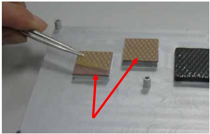
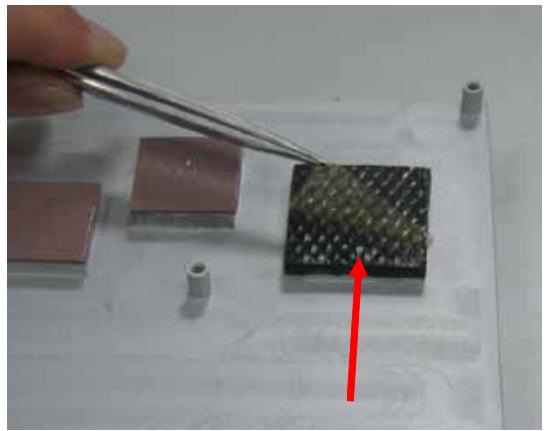
![Close-up of a hand using tweezers to sample a grid-patterned material sample on a white surface (no text or symbols visible)](.etx-at-50-1j020-1020-202/80d63b4ab9c7f233258045e7b432420c0a1b2bd3d262c8e566180a7ffc6a65ad.jpg)

![Close-up of a hand using tweezers to apply material to a microplate with a red arrow pointing to it (no text or symbols visible)](.etx-at-50-1j020-1020-202/da7c8aea2aa54feb6714a6b51e43ee8502c3b9cc0fb962df70bb67dd26e7b88e.jpg)

Remove the protective layer from CPU, Northbridge, and Southbridge pads before placing the heatspreader on the module.
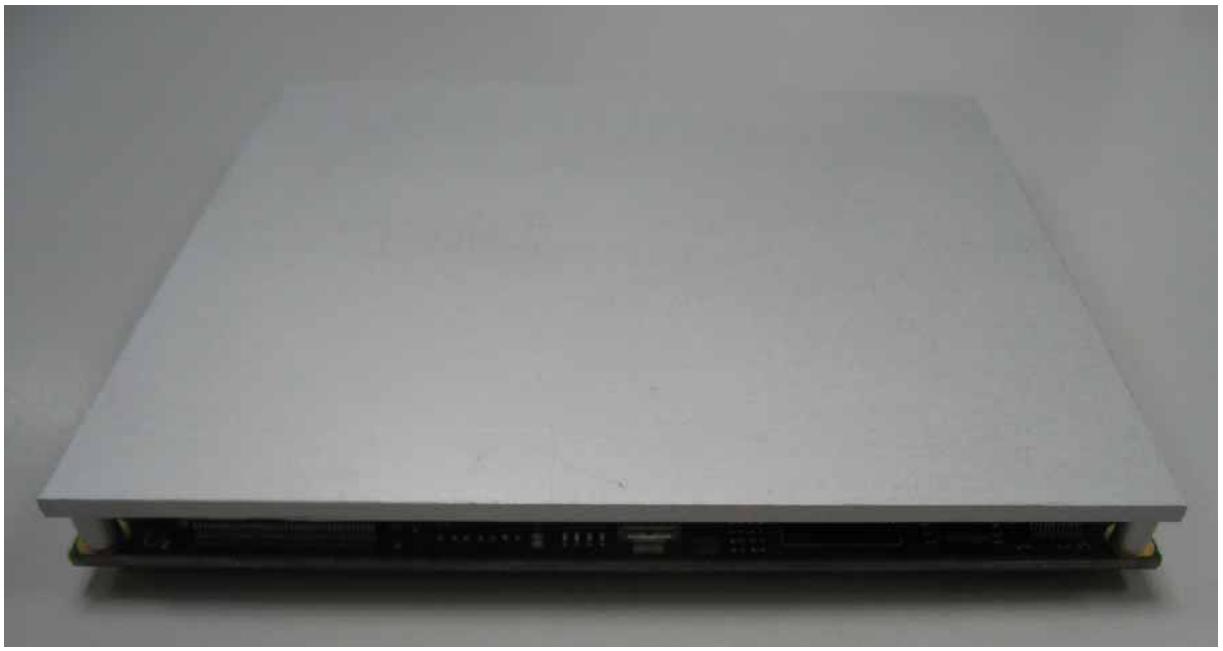
![Exterior view of a white electronic device with circuit board and indicator lights (no visible text or symbols)](.etx-at-50-1j020-1020-202/b91a149f434c59258c1fe6a4ad49a2652d913e0827c9ec8c4c31134e817cbc89.jpg)

Heatspreader mounted on ETX-AT

B.2 Heatspreader Dimensions for HTS-EAT-B (threaded type)
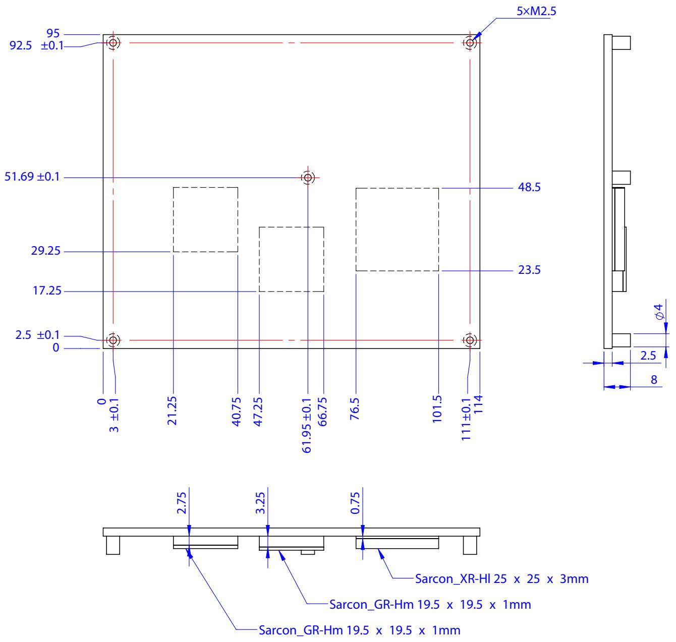
![The image displays a technical engineering drawing with three distinct views containing dimensions and specifications.\n\n**Top View:**\n*   **Left Dimensions:** '95', '92.5 ±0.1', '51.69 ±0.1', '29.25', '17.25', '2.5 ±0.1', '0'.\n*   **Bottom Horizontal Dimensions:** '0', '3 ±0.1', '21.25', '40.75', '47.25', '61.95 ±0.1', '66.75', '76.5', '101.5', '111 ±0.1', '114'.\n*   **Right Vertical Dimensions:** '48.5', '23.5'.\n*   **Top Right Annotation:** '5xM2.5'.\n\n**Right Side View:**\n*   **Dimensions:** '2.5', '8'.\n*   **Diameter:** 'Ø4'.\n\n**Bottom Detail View:**\n*   **Vertical Measurements:** '2.75', '3.25', '0.75'.\n*   **Component Labels:**\n    *   'Sarcon_XR-HI 25 x 25 x 3mm'\n    *   'Sarcon_GR-Hm 19.5 x 19.5 x 1mm'\n    *   'Sarcon_GR-Hm 19.5 x 19.5 x 1mm'](.etx-at-50-1j020-1020-202/b0821e9dae8a7231e6edd2e92971c80a5fcb26c54cad5c44ac677cb70744cb99.jpg)
The heatspreader comes with four M2.5 x L12mm screws with washer/spring for use with 3 mm standoffs on the carrier board, and M2.5 x L16mm screws with washer/spring for use with 9.5 mm standoffs on the carrier board. (If the heatspreader is purchased separately, one M2.5 x L6mm screw is also included.)

B.3 Heatspreader Dimensions for HTS-EAT-BT (through-hole type)
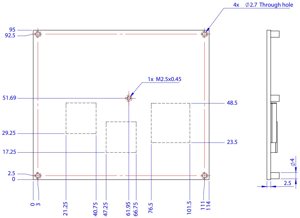
![| Dimension | Value |\n| --------- | ----- |\n| Height    | 95    |\n| Width     | 92.5  |\n| Top Margin | 4x    |\n| Bottom Margin | 1x   |\n| Intersection | 1x M2.5x0.45 |\n| Base Diameter | 3   |\n| Total Width | 21.25 |\n| Total Height | 40.75 |\n| Total Height | 47.25 |\n| Total Height | 61.95 |\n| Total Height | 66.75 |\n| Total Height | 76.5 |\n| Total Height | 101.5 |\n| Total Height | 111 |\n| Total Height | 114 |\n| Total Height | 2.5   |\n| Total Height | 23.5  |\n| Total Height | 48.5  |\n| Total Height | 2.5   |\n| Total Height | 4     |](.etx-at-50-1j020-1020-202/1a13a8062ab2f8e4d795a9764bc94adffb9e6eca5c5b6868e6c550ef4f6519f0.jpg)

![2.75\n3.25\n0.75\nSarcon_XR-HI 25 x 25 x 3mm\nSarcon_GR-Hm 19.5 x 19.5 x 1mm\nSarcon_GR-Hm 19.5 x 19.5 x 1mm](.etx-at-50-1j020-1020-202/e8a4ee91e4ef8340c29d5aafcdffd90fd4fc519547c3b893dc0fae86b4d8d32e.jpg)

f The heatspreader comes with four M2.5 x L14mm screws with washer/spring. (If the heatspreader is purchased separately, one M2.5 x L6mm screw is also included.)

# B.4 Heatsinks: THS-EAT-B and THSH-EAT-BL (threaded type)

The THS-EAT-B Heatsink is a low profile heatsink that is optimized for reduced height applications. The THSH-EAT-BL Heatsink is a high profile heatsink for applications without reduced height restrictions. Although the heatsinks are fanless, they still require some airflow to efficiently cool applications. The heatsinks are available in two cooling fin orientations (“vertical” shown for the THS-EAT-B and “horizontal” shown for the THSH-EAT-BL) and are bottom mounting (threaded type).
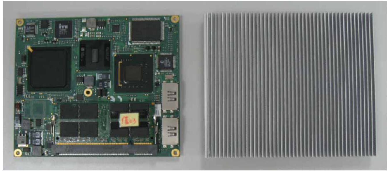
![Two electronic components: a green circuit board with various chips and connectors, and a metallic heat sink on a flat surface (no visible text or symbols)](.etx-at-50-1j020-1020-202/dbda768e5c7b5846619224a7447c576964f38ff02b7a79448ab9006282df89fb.jpg)

ETX-AT with THS-EAT-B heatsink (“vertically” oriented fins)
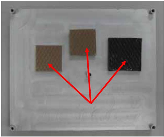
![Three square blocks with textured surfaces and red arrows pointing outward from a central point, no visible text or symbols.](.etx-at-50-1j020-1020-202/dfcae0da659565f6f70538e56c54aa1a7de30453b90fc0074947838f275ad58c.jpg)

Pads for CPU, Northbridge, and Southbridge

![The image features an icon of a white document with a folded top-right corner and faint horizontal lines. A large red checkmark is centered on the document. Below the icon is the text 'NOTE:' in black capital letters.](.etx-at-50-1j020-1020-202/6d882ce5ec485f7825c9493ad4088f8d00c587aa36bbf30f6001e53ddb139e4b.jpg)
Remove the protective layer from CPU, Northbridge, and Southbridge pads before placing the heatsink on the module (see Appendix B.1).
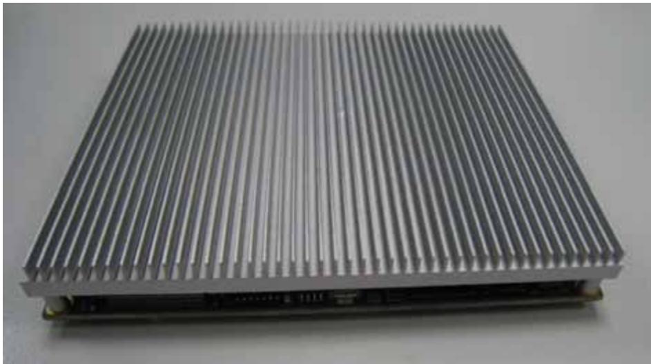
![Exterior view of a metallic heat sink with radial fins (no text or symbols visible)](.etx-at-50-1j020-1020-202/338c13302cc2d6723ad5ebb9d449d7e18545fc9aa3dd1f0a57182ff29397f50a.jpg)

THS-EAT-B Low Profile Heatsink mounted on ETX-AT
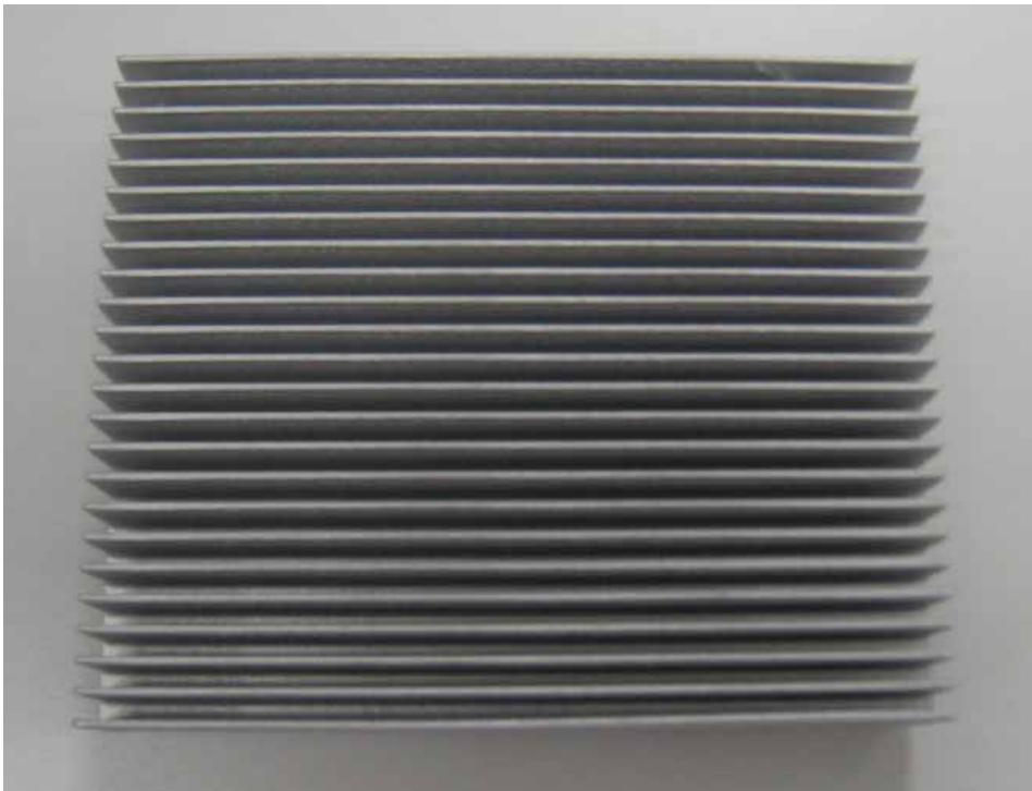
![Stacked metallic heat sink with uniform ridges (no text or symbols visible)](.etx-at-50-1j020-1020-202/9af85dc3d1311dfa8417ccdbd095fd3cdaa97e2401b426f2f22c783a2a126882.jpg)

THSH-EAT-BL High Profile Heatsink (“horizontally” oriented fins)

# B.5 Dimensions for THS-EAT-B Heatsink

# THS-EAT-B

Low profile heatsink with “vertically” oriented fins for bottom mounting.
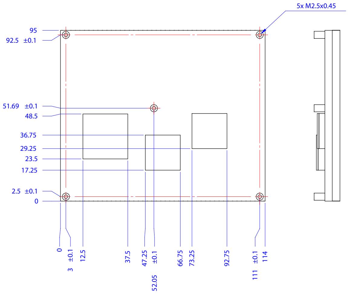
![| Dimension | Value     |\n| --------- | --------- |\n| Top Left   | 92.5 ±0.1 |\n| Top Right  | 51.69 ±0.1 |\n| Bottom Left| 2.5 ±0.1  |\n| Bottom Right| 111 ±0.1  |](.etx-at-50-1j020-1020-202/9055ab425fa0d480672466eba42005fabf14c84a1df53dc490818e31cc420132.jpg)

![Sarcon_GR-Hm 19.5 x 19.5 x 1mm\nSarcon_GR-Hm 19.5 x 19.5 x 1mm\nSarcon_XR-HI 25 x 25 x 3mm\n1.25\n3.75\n3.25\n4\n6\n8.4](.etx-at-50-1j020-1020-202/42cf4cd4f28dd0e52716bd02c71e506f873160ba61f0c0714ba9165f237250ac.jpg)

f The heatsink comes with four M2.5 x L12mm screws with washer/spring for use with 3 mm standoffs on the carrier board, and M2.5 x L16mm screws with washer/spring for use with 9.5 mm standoffs on the carrier board. (If the heatsink is purchased separately, one M2.5 x L6mm screw is also included.)

# B.6 Dimensions for THSH-EAT-BL Heatsink

# THSH-EAT-BL

High profile heatsink with “horizontally” oriented fins for bottom mounting.
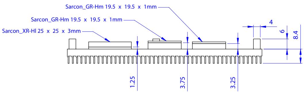
![| Dimension | Value     |\n| --------- | --------- |\n| Top Left   | 95        |\n| Top Right | 92.5 ±0.1 |\n| Bottom Left | 51.69 ±0.1 |\n| Bottom Right | 48.5    |\n| Bottom Center | 36.75   |\n| Bottom Center | 29.25   |\n| Bottom Center | 23.5    |\n| Bottom Center | 17.25   |\n| Bottom Center | 2.5 ±0.1 |\n| Bottom Right | 111 ±0.1 |\n| Bottom Center | 114       |\n| Vertical Line | 3 ±0.1, 12.5, 37.5, 47.25, 52.05, 66.75, 73.25, 92.75, 111, 18.1 |](.etx-at-50-1j020-1020-202/b6b659204a45c524c5ad48e790bd4495bdb6d423f294e7d5451aeebcbca7d59e.jpg)

![Sarcon_GR-Hm 19.5 x 19.5 x 1mm\nSarcon_GR-Hm 19.5 x 19.5 x 1mm\nSarcon_XR-HI 25 x 25 x 3mm\n1.25\n3.75\n3.25\n4](.etx-at-50-1j020-1020-202/a4e6f727894fd357e9576b914b3a7a508eb5449b464a3f9d4662a842f6bdf3a1.jpg)

f The heatsink comes with four M2.5 x L12mm screws with washer/spring for use with 3 mm standoffs on the carrier board, and M2.5 x L16mm screws with washer/spring for use with 9.5 mm standoffs on the carrier board. (If the heatsink is purchased separately, one M2.5 x L6mm screw is also included.)

# Important Safety Instructions

For user safety, please read and follow all instructions, warnings, cautions, and notes marked in this manual and on the associated equipment before handling/operating the equipment.

f Read these safety instructions carefully.
f Keep this user’s manual for future reference.
f Read the specifications section of this manual for detailed information on the operating environment of this equipment.
f When installing/mounting or uninstalling/removing equipment:

\- Turn off power and unplug any power cords/cables.

f To avoid electrical shock and/or damage to equipment:

- Keep equipment away from water or liquid sources;
- Keep equipment away from high heat or high humidity;
- Keep equipment properly ventilated (do not block or cover ventilation openings);
- Make sure to use recommended voltage and power source settings;
Always install and operate equipment near an easily accessible electrical socket-outlet;
- Secure the power cord (do not place any object on/over the power cord);
- Only install/attach and operate equipment on stable surfaces and/or recommended mountings; and,
- If the equipment will not be used for long periods of time, turn off and unplug the equipment from its power source.

f Never attempt to fix the equipment. Equipment should only be serviced by qualified personnel.
f A Lithium-type battery may be provided for uninterrupted, backup or emergency power.

![The image displays a low-resolution, pixelated warning sign. It features a yellow triangle with a black border containing a large black exclamation point in the center. Below the triangle, the word 'CAUTION:' is written in bold, black, capital letters.](.etx-at-50-1j020-1020-202/47f00c0fa9a230ea1c8396ce62a25ba4ce523edfb855afe99e53c9e24be1c37e.jpg)

Risk of explosion if battery is replaced by an incorrect type. Dispose of used batteries according to the instructions.

f Equipment must be serviced by authorized technicians when:

- The power cord or plug is damaged;
- Liquid has penetrated the equipment;
- It has been exposed to high humidity/moisture;
- It is not functioning or does not function according to the user’s manual;
- It has been dropped and/or damaged; and/or,
- It has an obvious sign of breakage.

# Getting Service

Contact us should you require any service or assistance.

# ADLINK Technology Inc.

Address: 9F, No.166 Jian Yi Road, Chungho City, Taipei County 235, Taiwan ؀קᗼխࡉؑ৬ԫሁ166ᇆ 9ᑔ

Tel: +886-2-8226-5877

Fax: +886-2-8226-5717

Email: service@adlinktech.com

# Ampro ADLINK Technology Inc.

Address: 5215 Hellyer Avenue, #110, San Jose, CA 95138, USA

Tel: +1-408-360-0200

Toll Free: +1-800-966-5200 (USA only)

Fax: +1-408-360-0222

Email: info@adlinktech.com

# ADLINK Technology Beijing

Address: ࣫ҀᏖ⍋⎔ऎϞഄϰ䏃 1 োⲜ߯ ࡯ࡼ ໻ॺ E ᑻ 801 ᅸ (100085) Rm. 801, Power Creative E, No. 1, B/D Shang Di East Rd., Beijing 100085, China

Tel: +86-10-5885-8666

Fax: +86-10-5885-8625

Email: market@adlinktech.com

# ADLINK Technology Shanghai

Address: Ϟ⍋Ꮦⓩ⊇⋒催⾥ᡔᓔথऎ䩺∳䏃 333 ো 39 ᐶ 4 ሖ (200233)

Tel: +86-21-6495-5210

Fax: +86-21-5450-0414

Email: market@adlinktech.com

# ADLINK Technology Shenzhen

Address: ⏅ഇᏖफቅऎ⾥ᡔುफऎ催ᮄफϗ䘧᭄ᄫᡔᴃು A1 ᷟ 2 ὐ C ऎ (518057)

2F, C Block, Bld. A1, Cyber-Tech Zone,

Gao Xin Ave. Sec 7, High-Tech Industrial Park S.,

Shenzhen, 518054 China

Tel: +86-755-2643-4858

Fax: +86-755-2664-6353

Email: market@adlinktech.com

# ADLINK Technology Inc. (German Liaison Office)

Address: Nord Carree 3, 40477 Duesseldorf, Germany

Tel: +49-211-495-5552

Fax: +49-211-495-5557

Email: emea@adlinktech.com

# ADLINK (French Liaison Office)

Address: 15 rue Emile Baudot, 91300 MASSY Cedex, France

Tel: +33 (0) 1 60 12 35 66

Fax: +33 (0) 1 60 12 35 66

Email: france@adlinktech.com

# ADLINK Technology Japan Corporation

Address: 151-0072 ᧲੩ㇺᷦ⼱඙ᐈ䊱⼱

1-1-2 ᦺᣣ↢๮ᐈ䊱⼱䊎䊦 8F

Asahiseimei Hatagaya Bldg. 8F

1-1-2 Hatagaya, Shibuya-ku, Tokyo 151-0072, Japan

Tel: +81-3-4455-3722

Fax: +81-3-5333-6040

Email: japan@adlinktech.com

# ADLINK Technology Inc. (Korean Liaison Office)

Address: 昢殾柢 昢爎割 昢爎壟 1506-25 穢壊 B/D 2 猻

2F, Hando B/D, 1506-25, Seocho-Dong,

Seocho-Gu, Seoul, 137-070, Korea

Tel: +82-2-2057-0565

Fax: +82-2-2057-0563

Email: korea@adlinktech.com

# ADLINK Technology Singapore Pte Ltd.

Address: 84 Genting Lane #07-02A, Cityneon Design Centre,

Singapore 349584

Tel: +65-6844-2261

Fax: +65-6844-2263

Email: singapore@adlinktech.com

# ADLINK Technology Singapore Pte Ltd. (Indian Liaison Office)

Address: No. 1357, "Anupama", Sri Aurobindo Marg, 9th Cross,

JP Nagar Phase I, Bangalore - 560078, India

Tel: +91-80-65605817

Fax: +91-80-22443548

Email: india@adlinktech.com

![The image displays a black circle containing a white recycling symbol in the center. The symbol consists of three arrows arranged in a triangular loop, curving in a clockwise direction. Each arrow features three parallel lines running along the outer side of its shaft. The image is low-resolution and pixelated. There is no text present.](.etx-at-50-1j020-1020-202/c60abaa86aeced78ab162375d2fe36439b80d233a96bfc8be96b4c5cf10aab47.jpg)
[🔗 Link to the original document](.etx-at-50-1j020-1020-202/etx-at-50-1j020-1020-202.pdf)