#

# ETX-GLX

# User’s Manual

![Close-up of a green printed circuit board with multiple integrated circuits and connectors (no readable text or symbols)](.etx-glx-50-1j008-1020-211/80f7c081f2a77b9ebdfc7d5bfece5853f589be7d5b045e0727da0467d04c57ca.jpg)

Manual Revision: 2.11

Revision Date: March 17, 2009

Part Number: 50-1J008-1020

Revision History

<table><tr><td>Release</td><td>Date</td><td>Change(s)</td></tr><tr><td>2.00</td><td>2007/11/09</td><td>Initial release</td></tr><tr><td>2.01</td><td>2007/11/15</td><td>LVDS Specification correction</td></tr><tr><td>2.10</td><td>2008/07/24</td><td>Correct Functional DiagramCorrect VGA specificationCorrect System Resources (I/O Address Map)Correct BIOS chapter (Advanced BIOS Features, Advanced Chipset Features)Correct address, revise layout</td></tr><tr><td>2.11</td><td>2009/03/17</td><td>Add &quot;single channel 18-bit LVDS support by BOM option&quot;</td></tr></table>

# Table of Contents

# ETX-GLX..

# Preface . 5

# 1 Introduction ..

# 2 Specifications .. 8

2.1 General . 8
2.2 Display .......... 8
2.3 Multi I/O 9
2.4 Audio .. 9
2.5 LAN . 9
2.6 Power Supply and Environment .. .. 10

# 3 Functional Diagram . 11

# 4 Mechanical Dimensions . . 12

# 5 Watchdog Timer .. 1 3

# 6 Connectors.. . 16

6.1 Connector Location . . 16
6.2 Pin Compatibility . . 16
6.3 X1 Connector: PCI-bus, USB, & Audio . 17
6.4 X2 Connector: ISA Bus . .. 18
6.5 X3 Connector: CRT, LCD (LVDS), & Video ...... .. 19
6.6 X3 Connector: COM1/2, LPT1 or FDD, IrDA, Mouse, & Keyboard . .. 20
6.7 X4 Connector: IDE1, IDE2, Ethernet, & Miscellaneous . . 21

# 7 System Resources.. 22

7.1 System Memory Map . 22
7.2 Direct Memory Access Channels . 22
7.3 I/O Address Map . . 23
7.4 Interrupt Request (IRQ) Lines . . 24
7.5 PCI Configuration Space Map .......... .. 25
7.6 PCI Interrupt Routing Map ......... .. 25
7.7 System Management Bus (I2C-compatible).. . 26

# 8 Phoenix Award BIOS . 27

8.1 Description ...... . 27
8.2 Main Menu Setup Items ....... . 28
8.3 Standard CMOS Features .... . 29
8.4 Advanced BIOS Features . . 33
8.5 Advanced Chipset Features . . 36
8.6 Integrated Peripherals . . 38
8.7 Power Management Setup.. . 40
8.8 PnP/PCI Configurations . . 42
8.9 PC Health Status . . 43

# Appendix A: Onboard DIP Switch for Power Mode Settings . . 44

A.1 Onboard DIP switch location and function . .. 44
A.2 AT/ATX Mode Settings . . 44

# Appendix B: Heatspreaders . . 45

B.1 Carrier Board ETX connecter heights (Hirose FX8/FX8C Receptacles) .. 45
B.2 Heatspreader Introduction.. . 46
B.3 Mounting procedures . 47
B.4 Standoffs .. .. 48
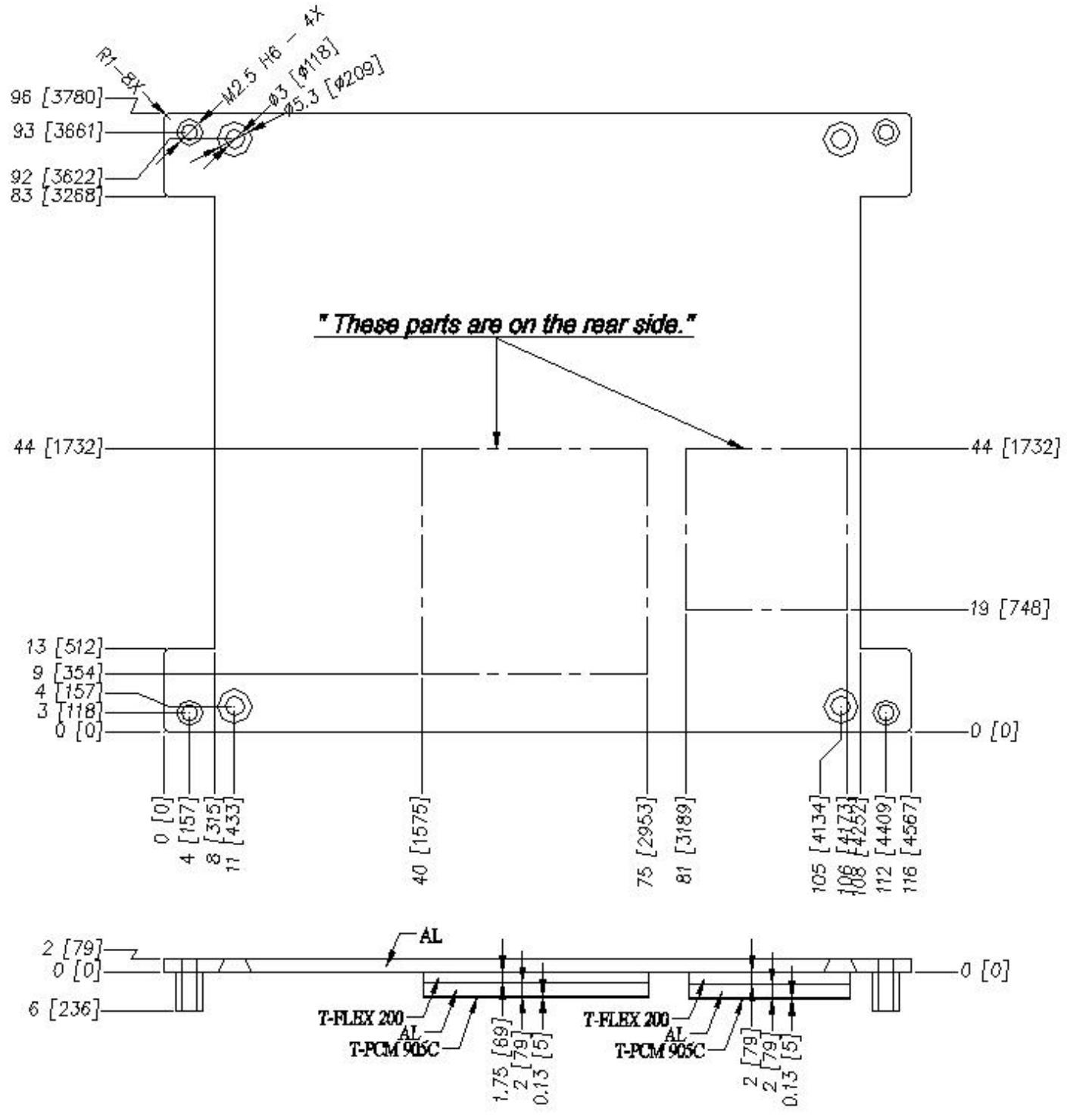
B.5 Heatspreader Dimensions for HTS-GLX .. .. 49
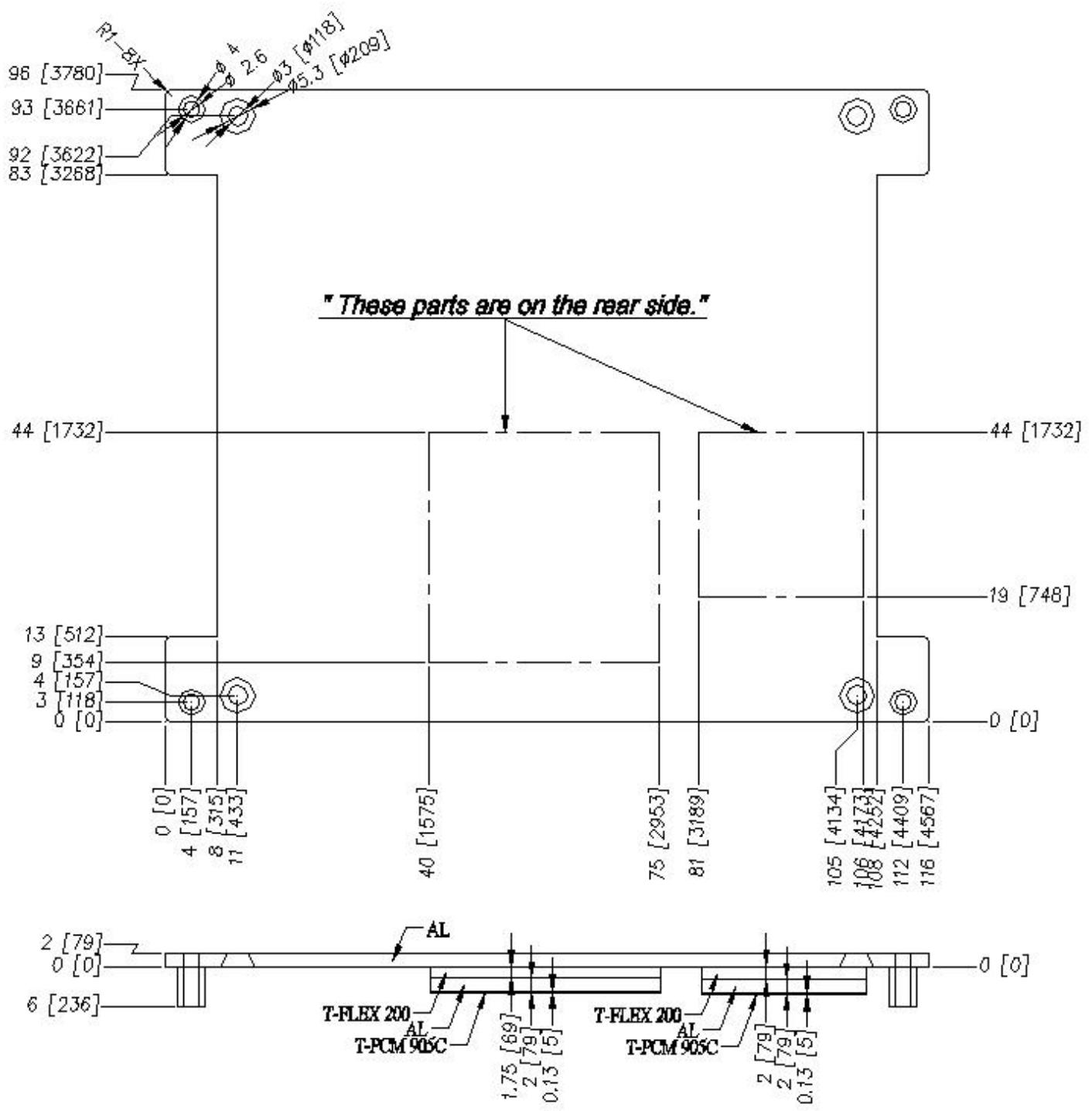
B.6 Heatspreader Dimensions for HTS-GLX-T . . 50
# Important Safety Instructions . 52

# Getting Service . . 54

# Preface

# Copyright 2009 ADLINK Technology, Inc.

This document contains proprietary information protected by copyright. All rights are reserved. No part of this manual may be reproduced by any mechanical, electronic, or other means in any form without prior written permission of the manufacturer.

# Disclaimer

The information in this document is subject to change without prior notice in order to improve reliability, design, and function and does not represent a commitment on the part of the manufacturer.

In no event will the manufacturer be liable for direct, indirect, special, incidental, or consequential damages arising out of the use or inability to use the product or documentation, even if advised of the possibility of such damages.

# Trademarks

ETX® is a registered trademark of Kontron Embedded Modules GmbH. Product names mentioned herein are used for identification purposes only and may be trademarks and/or registered trademarks of their respective companies.

# Conventions

Take note of the following conventions used throughout this manual to make sure that users perform certain tasks and instructions properly.

![The image displays a white document icon with faint horizontal lines, overlaid with a large red checkmark. Below the icon is the text 'NOTE:' in bold black letters.](.etx-glx-50-1j008-1020-211/f487c0d3c9bedff3d5c7eb641733ea49d59e51fd3f2d31f60e1d9ab3e6b8e2bd.jpg)

Additional information, aids, and tips that help users perform tasks.

![The image displays a yellow triangular warning sign containing a black exclamation point in the center. Directly below the triangle, the word 'CAUTION:' is printed in black capital letters.](.etx-glx-50-1j008-1020-211/86776e28d46f54248684b619064ab2daa7e31f617b123878761cd0924f419726.jpg)

Information to prevent minor physical injury, component damage, data loss, and/or program corruption when trying to complete a task.

![This image displays a triangular warning label with a black border. Inside the triangle is a red gradient background featuring a large white exclamation point in the center. Below the triangle, the word 'WARNING:' is printed in bold, black, capital letters.](.etx-glx-50-1j008-1020-211/3fc089ebba186923b78ea48dcb9845dd6e578f9bbb3b388fb3d5a3402a1c0605.jpg)

Information to prevent serious physical injury, component damage, data loss, and/or program corruption when trying to complete a specific task.

# 1 Introduction

ETX-GLX is a low power ETX® module that complies with the new ETX® revision 3.02 form factor specifications. ETX® revision 3.02 adds two SATA port connectors to the ETX module while maintaining full backward compatibility with the previous ETX® rev 2.x designs. Therefore existing ETX® carrier board do not have to be modified to be able to use this new SATA storage feature.

The Computer on Module concept of off-the-shelf core modules, combined with custom made carrier boards, dramatically reduces product development time and time to market. With all major functions already included on the Computer on Module, system developers and OEM can now concentrate on their core competencies and unique system values of their product. The ETX form factor is competitively priced for OEM projects with production quantities ranging from 500 to 50,000 pieces.

The new ETX-GLX targets markets for Medical Automation, Gaming, Instrumentation, POS, Mobile Computing and Transportation where low power, medium performance and extended graphic support is required.

The ETX-GLX, based on AMD's Geode™ LX 800 processor and CS5536 companion chipset, constitutes the perfect balance between computing performance and low power consumption. It supports up to 1 GB DDR400 in a single SODIMM socket or optionally can be equipped with 128 MB or 256 MB DDR400 memory soldered on the module.

The module supports advanced display features such as high resolution Analog VGA support up to 1920 x 1440 and single or dual channel 24-bit LVDS panels at max. 1600 x 1200 resolution. The board can optionally be equipped with an advanced Focus TV Encoder Chip that supports Standard Definition and High Definition TV Output, The Focus FS 455 covers a wide TV resolution spectrum, from standard NTSC/PAL, through 480p, 720p to 1080i.

The module further incorporates an Intel based 10/100Base-T Ethernet port, an PATA EIDE controller supporting both PIO and UDMA modes, a dual port SATA controller, 4 USB v2.0 ports, two serial ports, one parallel port (SPP/ECP/EPP) shared with FDD, one PS2 keyboard/mouse interface, AC’97 audio interface and power management functionality.

The ETX-GLX has full support for PCI and legacy ISA and comes with embedded features such as Watchdog controller, RS-232 console redirection and CMOS EEPROM backup for BIOS settings and battery-less operation. The ETX-GLX is a revision controlled product aimed at applications that require a guaranteed long production life support.

ETX-GLX is a RoHS compliant and lead free product

![ADLINK\nGREEN\nRoHS Compliant](.etx-glx-50-1j008-1020-211/522497d0c4e7ca2a22b6198482fc68a4960256649646492c3ae8b8ec71dbaaa6.jpg)

# 2 Specifications

# 2.1 General

f Embedded Processor: AMD Geode™ LX 800 CPU 500 MHz.
f Chipset: Geode™ CS5536 companion device
f Memory: 128/256 MB of soldered onboard DDR 400 memory and one 200-pin socket for additional, up to 1 GB DDR 400 SODIMM. (Max. of soldered onboard plus socket memory is 1 GB)
f Cache: 128 KB L2 cache
f Enhanced IDE: two ports: one port supports two devices that can operate in PIO modes 0 to 4, MDMA modes 0 to 2, or UDMA modes 0 to 5 (up to 100 MB/s); another port from VIA 6421A, for two enhanced IDE devices, supports ATA PIO mode 4, multi-word DMA-mode 2 drivers and UltraDMA-mode6

![The image displays a small, pixelated icon featuring a white document with a folded top-right corner. A large red checkmark is superimposed over the document. Below the document graphic, the text 'NOTE:' is printed in black, capital letters.](.etx-glx-50-1j008-1020-211/aa5bd9d194a52b1924f2d73ad11a1963a595b1482ca18c1116d8eaf9f50b08ff.jpg)

The IDE port (secondary port) from VIA 6421A does not support CompactFlash®. For CompactFlash® support, please connect to the Primary IDE port.

f SATA: Complies with Serial ATA Specification Revision 1.0; Dual channel master mode PCI supporting up to two S-ATA devices.
f BIOS: AWARD 4 Mb Flash BIOS with ACPI 2.0 and APM power management with console redirection and CMOS backup in onboard EEPROM
f Hardware Monitor: integrated in Winbond W83627HG monitors supply voltages and CPU temperature
f Watchdog Timer: 255-level timer generates RESET
f Expansion: 16-bit ISA and 32-bit PCI 2.2

# 2.2 Display

f VGA: (integrated in AMD Geode™LX 800 CPU companion device)

- Supports up to 1920x1440x32 bpp resolution at 85 Hz
- Supports up to 1600x1200x32 bpp resolution at 100 Hz

f LVDS: (NS DS90C387A LVDS transmitter)

- Single or dual channel 24-bit
- Supports SVGA through QXGA panel resolutions
- Compatible with ANSI/TIA/EIA-644-1995 LVDS Standard
- Backward compatible with FPD-Link
- Single channel 18-bit LVDS support by BOM option

f TV OUT (optional): (Focus FS455)

- Supports NTSC and PAL spectrum output for 480p, 720p and 1080i resolution
- Programmable 2D scaling

# 2.3 Multi I/O

f Chipset: Winbond W83627HG
f Serial: 2 high speed RS-232C
- COM1 - 16550 UART: up to 115Kbits/sec
- COM2 - 16550 UART: up to 115Kbits/sec
f Parallel: SPP, EPP and ECP mode (pins shared with FDD)
f FDD: single FDD (pins shared with LPT1)
f IrDA: supports SIR IrDA 1.1 compliant
f USB: supports up to four ports ver 2.0
f Keyboard & Mouse: one PS/2 keyboard and one PS/2 mouse

# 2.4 Audio

f Chipset: included on CS5536
f Audio Codec: AC’97 type Realtek ALC655

# 2.5 LAN

f Chipset: Intel® 82551QM
f Interface: 10BASE-T/100BASE-TX with TCP/UDP/IP checksum off-loading and PXE boot support

# 2.6 Power Supply and Environment

f Power Requirements:

<table><tr><td colspan="6">AMD GeodeTM LX 800 with 256 MB soldered DDR400</td></tr><tr><td></td><td>+5 V(mA)</td><td>5 VSB(mA)</td><td>+5 V(W)</td><td>5 VSB(W)</td><td>Total(W)</td></tr><tr><td>Light Load</td><td>1216</td><td>153.2</td><td>6.08</td><td>0.766</td><td>6.08</td></tr><tr><td>Full Load</td><td>1438</td><td>153.2</td><td>7.19</td><td>0.766</td><td>7.19</td></tr></table>

<table><tr><td colspan="6">AMD GeodeTM LX 800 with 512 MB socket memory</td></tr><tr><td></td><td>+5 V(mA)</td><td>5 VSB(mA)</td><td>+5 V(W)</td><td>5 VSB(W)</td><td>Total(W)</td></tr><tr><td>Light Load</td><td>1346</td><td>164.1</td><td>6.73</td><td>0.821</td><td>6.73</td></tr><tr><td>Full Load</td><td>1522</td><td>164.1</td><td>7.61</td><td>0.821</td><td>7.61</td></tr></table>

f Operating Temperature: 0 °C to 60 °C (32 °F to 140 °F)
f Relative Humidity: up to 90% at $5 5 ^ { \circ } \mathrm { C }$
f ETX Board Dimensions: 95 mm x 114 mm (3.7" x 4.5")
f Weight: 72 grams without memory onboard, 74 grams with soldered memory

# 3 Functional Diagram

![The block diagram illustrates a motherboard architecture centered around an AMD Geode LX800 processor.\n\n**Labeled Blocks:**\n*   **X4**\n*   **CPU + North** (AMD Geode LX800 Processor)\n    *   *Internal blocks:* CRT, TTL, PCI Controller, DDR400 Memory Controller\n*   **DDR 400** (SODIMM Socket)\n*   **DDR 400 onboard**\n*   **LVDS** (dual channel, opt. TV out)\n*   **Ethernet** (Mac/PHY Intel 82551QM)\n*   **AC'97** (Codec ALC 655)\n*   **X1**\n*   **4x USB 2.0**\n*   **CS5536** (I/O Companion)\n    *   *Internal blocks:* I2C, Primary IDE, LPC, USB 2.0, Audio\n*   **PCI/SATA** (VIA 6421A)\n*   **SATA** (two blocks)\n*   **PCI/ISA Bridge** (IT8888G)\n*   **X2**\n*   **EEPROM** (CMOS backup)\n*   **BIOS**\n*   **LPC header**\n*   **Super I/O** (Winbond W83627HG)\n*   **X3**\n*   **IrDA**\n*   **Keyboard**\n*   **Mouse**\n*   **LPT1 / FDD**\n*   **COM1**\n*   **COM2**\n\n**Connections:**\n*   **CPU + North** connects to **LVDS**, **DDR 400** (SODIMM Socket), **DDR 400 onboard**, **Ethernet**, **PCI/SATA**, **PCI/ISA Bridge**, and **CS5536** (via a bus labeled **PCI ver. 2.2 - 33/66 MHz**).\n*   **CS5536** connects to **CPU + North**, **PCI/SATA**, **PCI/ISA Bridge**, **AC'97 Codec** (via internal **Audio** block), **EEPROM CMOS backup**, **Super I/O** (via internal **LPC** block), **4x USB 2.0** (via internal **USB 2.0** block), and **Ethernet** (via a line labeled **Secondary IDE**).\n*   **X4** connects to **LVDS**, **CPU + North** (via internal **CRT** block), and **Ethernet**.\n*   **PCI/SATA** connects to two **SATA** blocks.\n*   **PCI/ISA Bridge** connects to **X2** (via **ISA bus**).\n*   **AC'97 Codec** connects to **X1**.\n*   **4x USB 2.0** connects to **X1**.\n*   **Super I/O** connects to **BIOS**, **LPC header**, **IrDA**, **Keyboard**, **Mouse**, **LPT1 / FDD**, **COM1**, **COM2**, and **X3**.\n*   **X3** connects to **IrDA**, **Keyboard**, **Mouse**, **LPT1 / FDD**, **COM1**, and **COM2**.\n*   **BIOS** connects to **LPC header**.\n*   **DDR 400** (SODIMM Socket) connects to **DDR 400 onboard** (via a line labeled **Socket + Onboard Max. 1GB**).](.etx-glx-50-1j008-1020-211/32a945b3f6654364db8e4bea8a1487e4df1787c8ee83ee8861ec8b032a979254.jpg)

# 4 Mechanical Dimensions

![SIDE VIEW\nX4\nX2\nX1-X4 connectors on bottom side\nX3\nTOP VIEW\n5.15 (203)\n1.6 (63)\n95 (3740)\n92.5 (3642)\n87.5 (3445)\n87.15 (3431)\n70.4 (2772)\n53.3 (2098)\n41.7 (1642)\n24.6 (969)\n7.5 (295)\n2.5 (98)\n0 (0)\n0 (0)\n3 (118)\n2.4 (94)\n3.9 (154)\n10.02 (394)\n32.52 (1280)\n111 (4370)\n114 (4488)\n87.5 (3445)\n70.4 (2772)\n53.3 (2098)\n45.9 (1807)\n4-Ø1.1 (Ø43)\n28.8 (1134)\n11.7 (461)\n4-Ø0.7 (Ø28)\n110.1 (4335)\n111.6 (4394)](.etx-glx-50-1j008-1020-211/5e46bbc8fac267542daf03c7f052bb484b4482104a1620f4eb6a4698cae1fef9.jpg)

All tolerances ± 0.05 mm
Other tolerances ± 0.2 mm

# 5 Watchdog Timer

ETX-GLX implements a watchdog timer (WDT) embedded in the LPC based Winbond 83627HG Super I/O controller.

The Watchdog timer consists of a one-second/minute resolution counter (CRF6 of logical device 8 of 83627HG) and two Watchdog control registers (CRF5 and CRF7 of logical device 8). Once a value is set in the WDT, the timer begins to count down.

![Cartoon illustration of a bulldog wearing a red collar (no text or symbols)](.etx-glx-50-1j008-1020-211/ce07521b190eaf253d6f065d57853653b97850011c820f64afa64b090c9309e2.jpg)

Any movement in the keyboard, mouse, or software reset of the value will cause a reload of the timer value. The Watchdog output is connected to “reset”. When the system hangs up without software re-trigger, the system will be reset.

The Watchdog timer has a one second granularity up to 255 seconds or a one minute granularity up to 255 minutes. The keyboard and mouse will only reset the WDT if Bit 7 and 6 of CRF7 is set; that is values greater than C0h or 192 decimal.

To configure the registers, the following sequence should be followed:

f Writing 87h to location 2Eh twice to enter the extended function mode
f Configure the registers to set up the WDT
f Writing 0AAh to location 2Eh to exit the extended function mode

The sample code shown on the following pages resets the system after 15 seconds. Both keyboard and mouse interrupts will reload the WDT from CRF6.

WDT Sample Code
begin:
```txt
; Enter extended function mode, interrupt double-write
```

```csv
mov dx,2Eh
mov al,87h
out dx,al
out dx,al
mov dx,2Eh
mov al,2bh ;CR2B, bit4 -> 0 = WDTO
;bit4 -> 1 = GP24
out dx,al
mov dx,2Fh
mov al,0C0h
out dx,al
mov dx,2Eh
mov al,07h
out dx,al
mov dx,2Fh
mov al,08h ;device 8
out dx,al
mov dx,2Eh
mov al,30h
out dx,al
mov dx,2Fh
mov al,01h ;enable device 8
out dx,al
mov dx,2Eh
mov al,0F7h
out dx,al ;device 8, CRF7
mov dx,2Fh
mov al,0C0h
out dx,al
```

```asm
mov dx,2Eh
mov al,0F5h ;device 8, CRF5
out dx,al
mov dx,2Fh
mov al,00h ;bit3 -> 0 = second
;bit3 -> 1 = minute
out dx,al
mov dx,2Eh
mov al,0F6h ;device 8, CRF6
out dx,al
mov dx,2Fh
mov al,0Fh
out dx,al

;
; Exit extended function mode

;

mov dx,2Eh
mov al,0AAh
out dx,al

.exit

end
```

# 6 Connectors

# 6.1 Connector Location

![- Ethernet\n- IDE1/IDE2\n- Power Signals\n- Speaker, Battery\n- I²C & SMB bus\n\nX4](.etx-glx-50-1j008-1020-211/ef7739b786d66a02acb4a0388d05be29466462efdec7a37816c6aff703cb99b0.jpg)

![ETX® Core\nModule\n(top view)](.etx-glx-50-1j008-1020-211/008ac253d22216d4b8a4a64861f1b753ac2558ed79512f79f4d1a61b8be4bffb.jpg)

\- ISA bus

- 32-bit PCI bus
- USB
- Audio

![X3\n- VGA/LCD/Video\n- COM1/COM2\n- LPT1\n- IrDA\n- Mouse\n- Keyboard](.etx-glx-50-1j008-1020-211/cb18d8563d403e8b6f5a50375b92075f40ecf629a0c249dd4c9063caaea4496c.jpg)

# 6.2 Pin Compatibility

All pins on X1, X2, X3, and X4 of the ETX-GLX comply with pin and signal descriptions used in the ETX® Specification ver. 3.02. This document contains a description of pins, signal descriptions, and mechanical characteristics of the ETX® form factor.

An additional document, “ETX® Design Guide” gives a general introduction to carrier board designs for ETX® modules.

# 6.3 X1 Connector: PCI-bus, USB, & Audio

![The image displays a vertical black-and-white diagram of a rectangular component, resembling a dual in-line package connector. In the center is a tall white rectangle containing a smaller inner rectangle and a small notch at the top center. Flanking this central shape are two columns of small, vertical rectangular blocks representing pins. The number '99' appears at the top left corner, and '1' appears at the bottom left corner. The number '100' appears at the top right corner, and '2' appears at the bottom right corner.](.etx-glx-50-1j008-1020-211/4dd8533f43110d4e670d0b2e807cb4fef5e5bdf1152b0fb856e8a9c3bbeae486.jpg)

Signals and Pins

<table><tr><td>Pin</td><td>Signal</td><td>Pin</td><td>Signal</td></tr><tr><td>1</td><td>GND</td><td>2</td><td>GND</td></tr><tr><td>3</td><td>PCICLK3</td><td>4</td><td>PCICLK4</td></tr><tr><td>5</td><td>GND</td><td>6</td><td>GND</td></tr><tr><td>7</td><td>PCICLK1</td><td>8</td><td>PCICLK2</td></tr><tr><td>9</td><td>REQ3#</td><td>10</td><td>GNT3#</td></tr><tr><td>11</td><td>GNT2#</td><td>12</td><td> $3V^1$ </td></tr><tr><td>13</td><td>REQ2#</td><td>14</td><td>GNT1#</td></tr><tr><td>15</td><td>REQ1#</td><td>16</td><td> $3V^1$ </td></tr><tr><td>17</td><td>GNT0#</td><td>18</td><td>RSV</td></tr><tr><td>19</td><td>5VCC</td><td>20</td><td>5VCC</td></tr><tr><td>21</td><td>SERIRQ</td><td>22</td><td>REQ0#</td></tr><tr><td>23</td><td>AD0</td><td>24</td><td> $3V^1$ </td></tr><tr><td>25</td><td>AD1</td><td>26</td><td>AD2</td></tr><tr><td>27</td><td>AD4</td><td>28</td><td>AD3</td></tr><tr><td>29</td><td>AD6</td><td>30</td><td>AD5</td></tr><tr><td>31</td><td>CBE0#</td><td>32</td><td>AD7</td></tr><tr><td>33</td><td>AD8</td><td>34</td><td>AD9</td></tr><tr><td>35</td><td>GND</td><td>36</td><td>GND</td></tr><tr><td>37</td><td>AD10</td><td>38</td><td>AUXAL</td></tr><tr><td>39</td><td>AD11</td><td>40</td><td>MIC</td></tr><tr><td>41</td><td>AD12</td><td>42</td><td>AUXAR</td></tr><tr><td>43</td><td>AD13</td><td>44</td><td>ASVCC</td></tr><tr><td>45</td><td>AD14</td><td>46</td><td>SDNL</td></tr><tr><td>47</td><td>AD15</td><td>48</td><td>ASSGND</td></tr><tr><td>49</td><td>CBE1#</td><td>50</td><td>SNDR</td></tr></table>

<table><tr><td>Pin</td><td>Signal</td><td>Pin</td><td>Signal</td></tr><tr><td>51</td><td>5VCC</td><td>52</td><td>5VCC</td></tr><tr><td>53</td><td>PAR</td><td>54</td><td>SERR#</td></tr><tr><td>55</td><td>GPERR</td><td>56</td><td>RSV</td></tr><tr><td>57</td><td>PME#</td><td>58</td><td>USB2-</td></tr><tr><td>59</td><td>LOCK#</td><td>60</td><td>DEVSEL#</td></tr><tr><td>61</td><td>TRDY#</td><td>62</td><td>USB3-</td></tr><tr><td>63</td><td>IRDY#</td><td>64</td><td>STOP#</td></tr><tr><td>65</td><td>FRAME#</td><td>66</td><td>USB2+</td></tr><tr><td>67</td><td>GND</td><td>68</td><td>GND</td></tr><tr><td>69</td><td>AD16</td><td>70</td><td>CBE2#</td></tr><tr><td>71</td><td>AD17</td><td>72</td><td>USB3+</td></tr><tr><td>73</td><td>AD19</td><td>74</td><td>AD18</td></tr><tr><td>75</td><td>AD20</td><td>76</td><td>USB0N</td></tr><tr><td>77</td><td>AD22</td><td>78</td><td>AD21</td></tr><tr><td>79</td><td>AD23</td><td>80</td><td>USB1-</td></tr><tr><td>81</td><td>AD24</td><td>82</td><td>CBE3#</td></tr><tr><td>83</td><td>5VCC</td><td>84</td><td>5VCC</td></tr><tr><td>85</td><td>AD25</td><td>86</td><td>AD26</td></tr><tr><td>87</td><td>AD28</td><td>88</td><td>USB0+</td></tr><tr><td>89</td><td>AD27</td><td>90</td><td>AD29</td></tr><tr><td>91</td><td>AD30</td><td>92</td><td>USB1+</td></tr><tr><td>93</td><td>PCIRST#</td><td>94</td><td>AD31</td></tr><tr><td>95</td><td>INTC#</td><td>96</td><td>INTD#</td></tr><tr><td>97</td><td>INTA#</td><td>98</td><td>INTB#</td></tr><tr><td>99</td><td>GND</td><td>100</td><td>GND</td></tr></table>

![The image features a document icon with a large red checkmark in the center. Below the document icon, the text 'NOTE:' is written in black, uppercase letters.](.etx-glx-50-1j008-1020-211/3ba13b24c502240d801dc1b50d1d5b5d02224435b2068a156eca8557b9ac5454.jpg)

1 The 3V (3.3 V ±5%) is generated on-board. Pins may be used to power devices on the carrier board up to a maximum load of 500 mA.

![The image features a yellow triangular warning sign with a thick black border and a large black exclamation point centered inside. Directly below the triangle, the text 'CAUTION:' is printed in black capital letters.](.etx-glx-50-1j008-1020-211/c1451a8fcd3b8de25c3f97d9a36aa96dee0c21ae6c0af8bb397df48610c24fda.jpg)

DO NOT CONNECT THE 3V PIN TO AN EXTERNAL 3.3 V SUPPLY POWER

# 6.4 X2 Connector: ISA Bus

![The image displays a diagram featuring a central vertical rectangular outline with a smaller cutout near its top left edge. Flanking this central shape on both the left and right sides are vertical columns composed of small, stacked rectangular segments. Four numbers frame the diagram: '99' is at the top left, '100' is at the top right, '1' is at the bottom left, and '2' is at the bottom right.](.etx-glx-50-1j008-1020-211/6a30f4c899b02c24119dfece6b91badf356784d373e3b3f353fc343eb382532a.jpg)

Signals and Pins

<table><tr><td>Pin</td><td>Signal</td><td>Pin</td><td>Signal</td></tr><tr><td>1</td><td>GND</td><td>2</td><td>GND</td></tr><tr><td>3</td><td>SD14</td><td>4</td><td>SD15</td></tr><tr><td>5</td><td>SD13</td><td>6</td><td>MASTER#</td></tr><tr><td>7</td><td>SD12</td><td>8</td><td>DREQ7</td></tr><tr><td>9</td><td>SD11</td><td>10</td><td>DACK7#</td></tr><tr><td>11</td><td>SD10</td><td>12</td><td>DREQ6</td></tr><tr><td>13</td><td>SD9</td><td>14</td><td>DACK6#</td></tr><tr><td>15</td><td>SD8</td><td>16</td><td>DREQ5</td></tr><tr><td>17</td><td>MEMW#</td><td>18</td><td>DACK5#</td></tr><tr><td>19</td><td>MEMR#</td><td>20</td><td>DREQ0</td></tr><tr><td>21</td><td>LA17</td><td>22</td><td>DACK0#</td></tr><tr><td>23</td><td>LA18</td><td>24</td><td>IRQ14</td></tr><tr><td>25</td><td>LA19</td><td>26</td><td>IRQ15</td></tr><tr><td>27</td><td>LA20</td><td>28</td><td> $\text{IRQ12}^{\text{1}}$ </td></tr><tr><td>29</td><td>LA21</td><td>30</td><td>IRQ11</td></tr><tr><td>31</td><td>LA22</td><td>32</td><td>IRQ10</td></tr><tr><td>33</td><td>LA23</td><td>34</td><td>IO16#</td></tr><tr><td>35</td><td>GND</td><td>36</td><td>GND</td></tr><tr><td>37</td><td>SBHE#</td><td>38</td><td>M16#</td></tr><tr><td>39</td><td>SA0</td><td>40</td><td>OSC</td></tr><tr><td>41</td><td>SA1</td><td>42</td><td>BALE</td></tr><tr><td>43</td><td>SA2</td><td>44</td><td>TC</td></tr><tr><td>45</td><td>SA3</td><td>46</td><td>DACK2#</td></tr><tr><td>47</td><td>SA4</td><td>48</td><td>IRQ3</td></tr><tr><td>49</td><td>SA5</td><td>50</td><td>IRQ4</td></tr></table>

<table><tr><td>Pin</td><td>Signal</td><td>Pin</td><td>Signal</td></tr><tr><td>51</td><td>VCC</td><td>52</td><td>VCC</td></tr><tr><td>53</td><td>SA6</td><td>54</td><td>IRQ5</td></tr><tr><td>55</td><td>SA7</td><td>56</td><td>IRQ6</td></tr><tr><td>57</td><td>SA8</td><td>58</td><td>IRQ7</td></tr><tr><td>59</td><td>SA9</td><td>60</td><td>SYSCLK</td></tr><tr><td>61</td><td>SA10</td><td>62</td><td>REFSH#</td></tr><tr><td>63</td><td>SA11</td><td>64</td><td>DREQ1</td></tr><tr><td>65</td><td>SA12</td><td>66</td><td>DACK1#</td></tr><tr><td>67</td><td>GND</td><td>68</td><td>GND</td></tr><tr><td>69</td><td>SA13</td><td>70</td><td>DREQ3</td></tr><tr><td>71</td><td>SA14</td><td>72</td><td>DACK3#</td></tr><tr><td>73</td><td>SA15</td><td>74</td><td>IOR#</td></tr><tr><td>75</td><td>SA16</td><td>76</td><td>IOW#</td></tr><tr><td>77</td><td>SA18</td><td>78</td><td>SA17</td></tr><tr><td>79</td><td>SA19</td><td>80</td><td>SMEMR#</td></tr><tr><td>81</td><td>IOCHRDY</td><td>82</td><td>AEN</td></tr><tr><td>83</td><td>VCC</td><td>84</td><td>VCC</td></tr><tr><td>85</td><td>SD0</td><td>86</td><td>SMEMW#</td></tr><tr><td>87</td><td>SD2</td><td>88</td><td>SD1</td></tr><tr><td>89</td><td>SD3</td><td>90</td><td>NOWS#</td></tr><tr><td>91</td><td>DREQ2</td><td>92</td><td>SD4</td></tr><tr><td>93</td><td>SD5</td><td>94</td><td>IRQ9</td></tr><tr><td>95</td><td>SD6</td><td>96</td><td>SD7</td></tr><tr><td>97</td><td>IOCHK#</td><td>98</td><td>RSTDRV</td></tr><tr><td>99</td><td>GND</td><td>100</td><td>GND</td></tr></table>

# 6.5 X3 Connector: CRT, LCD (LVDS), & Video

Signals and Pins

<table><tr><td>Pin</td><td>Signal</td><td>Pin</td><td>Signal</td></tr><tr><td>1</td><td>GND</td><td>2</td><td>GND</td></tr><tr><td>3</td><td>R</td><td>4</td><td>B</td></tr><tr><td>5</td><td>HSY</td><td>6</td><td>G</td></tr><tr><td>7</td><td>VSY</td><td>8</td><td>DDCK</td></tr><tr><td>9</td><td>NC</td><td>10</td><td>DDDA</td></tr><tr><td>11</td><td>LCD16</td><td>12</td><td>LCD18</td></tr><tr><td>13</td><td>LCD17</td><td>14</td><td>LCD19</td></tr><tr><td>15</td><td>GND</td><td>16</td><td>GND</td></tr><tr><td>17</td><td>LCD13</td><td>18</td><td>LCD15</td></tr><tr><td>19</td><td>LCD12</td><td>20</td><td>LCD14</td></tr><tr><td>21</td><td>GND</td><td>22</td><td>GND</td></tr><tr><td>23</td><td>LCD8</td><td>24</td><td>LCD11</td></tr><tr><td>25</td><td>LCD9</td><td>26</td><td>LCD10</td></tr><tr><td>27</td><td>GND</td><td>28</td><td>GND</td></tr><tr><td>29</td><td>LCD4</td><td>30</td><td>LCD7</td></tr><tr><td>31</td><td>LCD5</td><td>32</td><td>LCD6</td></tr><tr><td>33</td><td>GND</td><td>34</td><td>GND</td></tr><tr><td>35</td><td>LCD1</td><td>36</td><td>LCD3</td></tr><tr><td>37</td><td>LCD0</td><td>38</td><td>LCD2</td></tr><tr><td>39</td><td>5VCC</td><td>40</td><td>5VCC</td></tr><tr><td>41</td><td>JILI_SDA</td><td>42</td><td>LTGO0</td></tr><tr><td>43</td><td>JILI_SCL</td><td>44</td><td>BLON#</td></tr><tr><td>45</td><td>NC</td><td>46</td><td>DIGON</td></tr><tr><td>47</td><td>COMP</td><td>48</td><td>Y</td></tr><tr><td>49</td><td>NC</td><td>50</td><td>C</td></tr></table>

![The image displays a black-and-white line drawing of a vertical rectangular object. Inside the main outline is a nested, narrower rectangle with a stepped indentation on its upper left side. Flanking the central shape on both the left and right are vertical columns of tick marks resembling ruler graduations. The text '99' is located at the top left, '100' at the top right, '1' at the bottom left, and '2' at the bottom right.](.etx-glx-50-1j008-1020-211/519fdaeac15b1b885274f36b45404597e5947a7323a51f8fa97e922f286cbc8c.jpg)

First LVDS Channel

<table><tr><td>Signal</td><td>LVDS Signal</td></tr><tr><td>LCD0</td><td>Txout 0-</td></tr><tr><td>LCD1</td><td>Txout 0+</td></tr><tr><td>LCD2</td><td>Txout 1-</td></tr><tr><td>LCD3</td><td>Txout 1+</td></tr><tr><td>LCD4</td><td>Txout 2-</td></tr><tr><td>LCD5</td><td>Txout 2+</td></tr><tr><td>LCD6</td><td>Txclk -</td></tr><tr><td>LCD7</td><td>Txclk +</td></tr><tr><td>LCD8*</td><td>Txout 3-</td></tr><tr><td>LCD9*</td><td>Txout 3+</td></tr></table>

Second LVDS Channel

<table><tr><td>Signal</td><td>LVDS Signal</td></tr><tr><td>LCD10*</td><td>Txout 0-</td></tr><tr><td>LCD11*</td><td>Txout 0+</td></tr><tr><td>LCD12*</td><td>Txout 1-</td></tr><tr><td>LCD13*</td><td>Txout 1+</td></tr><tr><td>LCD14*</td><td>Txout 2-</td></tr><tr><td>LCD15*</td><td>Txout 2+</td></tr><tr><td>LCD16*</td><td>Txclk -</td></tr><tr><td>LCD17*</td><td>Txclk +</td></tr><tr><td>LCD18*</td><td>Txout 3-</td></tr><tr><td>LCD19*</td><td>Txout 3+</td></tr></table>

\* NC for 18-bit single channel BOM option

# 6.6 X3 Connector: COM1/2, LPT1 or FDD, IrDA, Mouse, & Keyboard

![The image shows a vertical rectangular diagram resembling a ruler or measurement scale. The central area is a blank white rectangle. Flanking the left and right sides of this rectangle are columns of dense, fine vertical tick marks.\n\nFour numbers are positioned at the corners of the diagram:\n- Top left: **99**\n- Top right: **100**\n- Bottom left: **1**\n- Bottom right: **2**](.etx-glx-50-1j008-1020-211/602fb9757fae57af19a0b0d111c579998f87bca2e0a0dd3d089aaa3e2ddd154e.jpg)

# Signals and Pins

LPT Mode

<table><tr><td>Pin</td><td>Signal</td><td></td><td>Pin</td></tr><tr><td>51</td><td>LPT/FLPY#</td><td>52</td><td>RESERVED</td></tr><tr><td>53</td><td>5VCC</td><td>54</td><td>GND</td></tr><tr><td>55</td><td>STB#</td><td>56</td><td>AFD#</td></tr><tr><td>57</td><td>RESERVED</td><td>58</td><td>PD7</td></tr><tr><td>59</td><td>IRRX</td><td>60</td><td>ERR#</td></tr><tr><td>61</td><td>IRTX</td><td>62</td><td>PD6</td></tr><tr><td>63</td><td>RXD2</td><td>64</td><td>INIT#</td></tr><tr><td>65</td><td>GND</td><td>66</td><td>GND</td></tr><tr><td>67</td><td>RTS2#</td><td>68</td><td>PD5</td></tr><tr><td>69</td><td>DTR2#</td><td>70</td><td>SLIN#</td></tr><tr><td>71</td><td>DCD2#</td><td>72</td><td>PD4</td></tr><tr><td>73</td><td>DSR2#</td><td>74</td><td>PD3</td></tr><tr><td>75</td><td>CTS2#</td><td>76</td><td>PD2</td></tr><tr><td>77</td><td>TXD2</td><td>78</td><td>PD1</td></tr><tr><td>79</td><td>RI2#</td><td>80</td><td>PD0</td></tr><tr><td>81</td><td>5VCC</td><td>82</td><td>5VCC</td></tr><tr><td>83</td><td>RXD1</td><td>84</td><td>ACK#</td></tr><tr><td>85</td><td>RTS1#</td><td>86</td><td>BUSY</td></tr><tr><td>87</td><td>DTR1#</td><td>88</td><td>PE</td></tr><tr><td>89</td><td>DCD1#</td><td>90</td><td>SLCT#</td></tr><tr><td>91</td><td>DSR1#</td><td>92</td><td>MSCLK</td></tr><tr><td>93</td><td>CTS1#</td><td>94</td><td>MSDAT</td></tr><tr><td>95</td><td>TXD1</td><td>96</td><td>KBCLK</td></tr><tr><td>97</td><td>RI1#</td><td>98</td><td>KBDAT</td></tr><tr><td>99</td><td>GND</td><td>100</td><td>GND</td></tr></table>

FDD Mode

<table><tr><td>Pin</td><td>Signal</td><td>Pin</td><td>Signal</td></tr><tr><td>51</td><td>LPT/FLPY#</td><td>52</td><td>RESERVED</td></tr><tr><td>53</td><td>5VCC</td><td>54</td><td>GND</td></tr><tr><td>55</td><td>RESERVED</td><td>56</td><td>DENSEL</td></tr><tr><td>57</td><td>RESERVED</td><td>58</td><td>RESERVED</td></tr><tr><td>59</td><td>IRRX</td><td>60</td><td>HDSEL#</td></tr><tr><td>61</td><td>IRTX</td><td>62</td><td>RESERVED</td></tr><tr><td>63</td><td>RXD2</td><td>64</td><td>DIR#</td></tr><tr><td>65</td><td>GND</td><td>66</td><td>GND</td></tr><tr><td>67</td><td>RTS2#</td><td>68</td><td>RESERVED</td></tr><tr><td>69</td><td>DTR2#</td><td>70</td><td>STEP#</td></tr><tr><td>71</td><td>DCD2#</td><td>72</td><td>DSKCHG#</td></tr><tr><td>73</td><td>DSR2#</td><td>74</td><td>RDATA#</td></tr><tr><td>75</td><td>CTS2#</td><td>76</td><td>WP#</td></tr><tr><td>77</td><td>TXD2</td><td>78</td><td>TRK0#</td></tr><tr><td>79</td><td>RI2#</td><td>80</td><td>INDEX#</td></tr><tr><td>81</td><td>5VCC</td><td>82</td><td>5VCC</td></tr><tr><td>83</td><td>RXD1</td><td>84</td><td>DRV</td></tr><tr><td>85</td><td>RTS1#</td><td>86</td><td>MOT</td></tr><tr><td>87</td><td>DTR1#</td><td>88</td><td>WDATA#</td></tr><tr><td>89</td><td>DCD1#</td><td>90</td><td>WGATE#</td></tr><tr><td>91</td><td>DSR1#</td><td>92</td><td>MSCLK</td></tr><tr><td>93</td><td>CTS1#</td><td>94</td><td>MSDAT</td></tr><tr><td>95</td><td>TXD1</td><td>96</td><td>KBCLK</td></tr><tr><td>97</td><td>RI1#</td><td>98</td><td>KBDAT</td></tr><tr><td>99</td><td>GND</td><td>100</td><td>GND</td></tr></table>

# 6.7 X4 Connector: IDE1, IDE2, Ethernet, & Miscellaneous

![This is a black and white schematic diagram of a rectangular component, resembling an Integrated Circuit (IC). It features a central rectangle flanked by two columns of vertical lines representing pins. The corners are labeled with numbers: '99' at the top left, '100' at the top right, '1' at the bottom left, and '2' at the bottom right. A small notch is visible at the top center of the inner rectangle.](.etx-glx-50-1j008-1020-211/c6ad7efdccf491c3f87f9bdc4afbd4094086f87611700077b38459086f914fac.jpg)

Signals and Pins

<table><tr><td>Pin</td><td>Signal</td><td>Pin</td><td>Signal</td></tr><tr><td>1</td><td>GND</td><td>2</td><td>GND</td></tr><tr><td>3</td><td>5V_SB</td><td>4</td><td>PWGIN</td></tr><tr><td>5</td><td>PS_ON</td><td>6</td><td>SPEAKER</td></tr><tr><td>7</td><td>PWRBTN#</td><td>8</td><td>BATT</td></tr><tr><td>9</td><td>KBINH</td><td>10</td><td>LILED#</td></tr><tr><td>11</td><td> $RSMRST^1$ </td><td>12</td><td>ACTLED#</td></tr><tr><td>13</td><td> $ROMKBCS^2$ </td><td>14</td><td>SPDLED#</td></tr><tr><td>15</td><td> $EXT\_PRG^2$ </td><td>16</td><td> $I2CLK^3$ </td></tr><tr><td>17</td><td>5VCC</td><td>18</td><td>5VCC</td></tr><tr><td>19</td><td>OVCR#</td><td>20</td><td>NC</td></tr><tr><td>21</td><td>EXTSMI#</td><td>22</td><td> $I2DAT^3$ </td></tr><tr><td>23</td><td> $SMBCLK^3$ </td><td>24</td><td> $SMBDATA^3$ </td></tr><tr><td>25</td><td>S_CS3#</td><td>26</td><td>SMBALRT#</td></tr><tr><td>27</td><td>S_CS1#</td><td>28</td><td>NC</td></tr><tr><td>29</td><td>S_A2</td><td>30</td><td>P_CS3#</td></tr><tr><td>31</td><td>S_A0</td><td>32</td><td>P_CS1#</td></tr><tr><td>33</td><td>GND</td><td>34</td><td>GND</td></tr><tr><td>35</td><td>PDIAG_S</td><td>36</td><td>P_A2</td></tr><tr><td>37</td><td>S_A1</td><td>38</td><td>P_A0</td></tr><tr><td>39</td><td>S_INTRO</td><td>40</td><td>P_A1</td></tr><tr><td>41</td><td> $BATLOW^2$ </td><td>42</td><td> $GPE1^2$ </td></tr><tr><td>43</td><td>S_AK#</td><td>44</td><td>P_INTRO</td></tr><tr><td>45</td><td>S_RDY</td><td>46</td><td>P_AK#</td></tr><tr><td>47</td><td>S_IOR#</td><td>48</td><td>P_RDY</td></tr><tr><td>49</td><td>5VCC</td><td>50</td><td>5VCC</td></tr></table>

<table><tr><td>Pin</td><td>Signal</td><td>Pin</td><td>Signal</td></tr><tr><td>51</td><td>S_IOW#</td><td>52</td><td>P_IOR#</td></tr><tr><td>53</td><td>S_DRQ</td><td>54</td><td>P_IOW#</td></tr><tr><td>55</td><td>S_D15</td><td>56</td><td>P_DRQ</td></tr><tr><td>57</td><td>S_D0</td><td>58</td><td>P_D15</td></tr><tr><td>59</td><td>S_D14</td><td>60</td><td>P_D0</td></tr><tr><td>61</td><td>S_D1</td><td>62</td><td>P_D14</td></tr><tr><td>63</td><td>S_D13</td><td>64</td><td>P_D1</td></tr><tr><td>65</td><td>GND</td><td>66</td><td>GND</td></tr><tr><td>67</td><td>S_D2</td><td>68</td><td>P_D13</td></tr><tr><td>69</td><td>S_D12</td><td>70</td><td>P_D2</td></tr><tr><td>71</td><td>S_D3</td><td>72</td><td>P_D12</td></tr><tr><td>73</td><td>S_D11</td><td>74</td><td>P_D3</td></tr><tr><td>75</td><td>S_D4</td><td>76</td><td>P_D11</td></tr><tr><td>77</td><td>S_D10</td><td>78</td><td>P_D4</td></tr><tr><td>79</td><td>S_D5</td><td>80</td><td>P_D10</td></tr><tr><td>81</td><td>5VCC</td><td>82</td><td>5VCC</td></tr><tr><td>83</td><td>S_D9</td><td>84</td><td>P_D5</td></tr><tr><td>85</td><td>S_D6</td><td>86</td><td>P_D9</td></tr><tr><td>87</td><td>S_D8</td><td>88</td><td>P_D6</td></tr><tr><td>89</td><td>GPE2 $^{2}$ </td><td>90</td><td>CBLID_P#</td></tr><tr><td>91</td><td>RXD#</td><td>92</td><td>P_D8</td></tr><tr><td>93</td><td>RXD</td><td>94</td><td>S_D7</td></tr><tr><td>95</td><td>TXD#</td><td>96</td><td>P_D7</td></tr><tr><td>97</td><td>TXD</td><td>98</td><td>HDRST#</td></tr><tr><td>99</td><td>GND</td><td>100</td><td>GND</td></tr></table>

![The image displays a digital icon featuring a white document with a folded top-right corner and faint horizontal grey lines. A large red checkmark is superimposed over the document. Below the graphic, the text 'NOTE:' appears in black, capitalized letters.](.etx-glx-50-1j008-1020-211/118f930a1fb69ab6b0000189faae495588087ee134f13fc40799f2415af40e05.jpg)

1 May be affected by external circuitry to reset the power management logic of the ETX module. Most designs do not use and pin is not connected.

2 Reserved, do not connect

3 See also: section 7.7 System Management Bus (I2C-compatible)

4 Available, but not supported on the ETX-GLX

# System Resources

# 7.1 System Memory Map

<table><tr><td>Address Range (decimal)</td><td>Address Range (hex)</td><td>Size</td><td>Description</td></tr><tr><td>1024 KB - TOM</td><td>100000 - NA</td><td>NA</td><td>Note 1</td></tr><tr><td>960 KB - 1024 KB</td><td>F0000 - FFFFF</td><td>64 KB</td><td>System BIOS Area</td></tr><tr><td>928 KB - 960 KB</td><td>E0000 - EFFFF</td><td>64 KB</td><td>Extended System BIOS Area</td></tr><tr><td>800 KB - 928 KB</td><td>C8000 - E7FFF</td><td>160 KB</td><td>Expansion ROM, Note 2</td></tr><tr><td>768 KB - 800 KB</td><td>C0000 - C7FFF</td><td>32 KB</td><td>Onboard VGA BIOS, Note 2</td></tr><tr><td>640 KB - 768 KB</td><td>A0000 - BFFFF</td><td>128 KB</td><td>Video Buffer &amp; SMM space</td></tr><tr><td>0 KB - 640 KB</td><td>00000 - 7FFFF</td><td>640 KB</td><td>Conventional Memory</td></tr></table>

![The image shows a graphic icon featuring a white document with a folded top-right corner. A large red checkmark is positioned on the left side of the document, accompanied by faint grey horizontal lines and a subtle red diagonal swoosh. Below the document graphic is the text 'NOTE ::' in black capital letters.](.etx-glx-50-1j008-1020-211/5377f5fa52cc74233886699fef242dd432c517fcf35ac93bbf6a16955eddc30d.jpg)

1 T.O.M = Top of memory. Some memory ranges like frame buffer (8M to 254M set by BIOS setting) and ACPI reserved area are unavailable for use.

2 When another PCI VGA card is used, it may need more memory range than 32KB. The VGA BIOS area may be changed to 48 KB or 64 KB When secondary IDE channel has drive or onboard LAN PXE functionality is enabled, it will occupy memory from expansion ROM range. Otherwise, available expansion ROM area can be forwarded to ISA bus.

# 7.2 Direct Memory Access Channels

<table><tr><td>Channel Number</td><td>Data Width</td><td>System Resource</td></tr><tr><td>0</td><td>8-bits or 16-bits</td><td>Open, Note 1</td></tr><tr><td>1</td><td>8-bits or 16-bits</td><td>Parallel Port, Notes 1 &amp; 2</td></tr><tr><td>2</td><td>8-bits or 16-bits</td><td>Floppy Controller, Notes 1 &amp; 2</td></tr><tr><td>3</td><td>8-bits or 16-bits</td><td>Parallel Port, Notes 1 &amp; 2</td></tr><tr><td>4</td><td>8-bits or 16-bits</td><td>Reserved, Cascade Channel</td></tr><tr><td>5</td><td>16-bits</td><td>Open, Note 1</td></tr><tr><td>6</td><td>16-bits</td><td>Open, Note 1</td></tr><tr><td>7</td><td>16-bits</td><td>Open, Note 1</td></tr></table>

![The image displays a white document icon with a folded upper right corner. Centered on the page is a large red checkmark. Below the checkmark, the text 'NOTE:' appears in black capital letters.](.etx-glx-50-1j008-1020-211/1a42f63054c24b0419d893ce40dcb8d18eda4d15bc55f8f4ff925a5440a7d507.jpg)

1 DMA request from ISA bridge is no longer served by south bridge on this platform. These DMA channels can be free on LPC bus, not ISA bus.

2 Only one of floppy controller and parallel controller can be used due to common hardware interface. ECP mode of parallel port will occupy channel 1 or 3.

7.3 I/O Address Map

<table><tr><td>Address</td><td>Size</td><td>Description</td></tr><tr><td>0000 - 00FF</td><td>256 bytes</td><td>Motherboard Resources</td></tr><tr><td>01F0 - 01F7</td><td>8 bytes</td><td>Primary IDE Channels</td></tr><tr><td>0278 - 027F</td><td>8 bytes</td><td>Parallel Port 2 (LPT2), Note 1</td></tr><tr><td>0294 - 0297</td><td>4 bytes</td><td>Onboard Sensor Index/Data Port</td></tr><tr><td>02E8 - 02EF</td><td>8 bytes</td><td>Serial Port 4 (COM4), Note 2</td></tr><tr><td>02F8 - 02FF</td><td>8 bytes</td><td>Serial Port 2 (COM2), Note 2</td></tr><tr><td>0378 - 037F</td><td>8 bytes</td><td>Parallel Port 2 (LPT1), Note 1</td></tr><tr><td>03B0 - 03BB</td><td>12 bytes</td><td>Video (Monochrome)</td></tr><tr><td>03BC - 03BF</td><td>4 bytes</td><td>Parallel Port 3 (LPT3), Note 2</td></tr><tr><td>03C0 - 03DF</td><td>32 bytes</td><td>Video (VGA)</td></tr><tr><td>03E8 - 03EF</td><td>8 bytes</td><td>Serial Port 3 (COM3), Note 2</td></tr><tr><td>03F0 - 03F5</td><td>6 bytes</td><td>Diskette Controller, Note 1</td></tr><tr><td>03F6 - 03F7</td><td>2 bytes</td><td>Primary IDE Command/Status Ports</td></tr><tr><td>03F8 - 03FF</td><td>8 bytes</td><td>Serial Port 1 (COM1), Note 2</td></tr><tr><td>04D0 - 04D1</td><td>2 bytes</td><td>Motherboard Resources</td></tr><tr><td>1000 - 1FFF</td><td>4 K byte</td><td>SMBus control addresses</td></tr><tr><td>6100 - 61FF</td><td>256 bytes</td><td>GPIO control addresses</td></tr><tr><td>6200 - 62FF</td><td>256 bytes</td><td>Motherboard Resources</td></tr><tr><td>9D00 -9DFF</td><td>256 bytes</td><td>Power management configuration addresses</td></tr><tr><td>2000 - FFFF</td><td>NA</td><td>PCI Bus, Note 3</td></tr></table>

![The image displays a white document icon featuring faint horizontal grey lines representing text. Overlaid on the left side of the document is a large, bold red checkmark.](.etx-glx-50-1j008-1020-211/235b6513d14778d71ff5d792c996863f243d7a6d7e0d84a1238a14952fcf47fb.jpg)
NOTE:

1 The occupancy of I/O range depends on BIOS setting, only one I/O range will be used and the others are forwarded to LPC bus.

2 The occupancy of I/O range depends on BIOS setting. If external Super I/O controller is present for two external serial ports on ISA bus, the I/O range must be set in BIOS in order to make sure they are really for warded to ISA bus.

3 The BIOS assigns PCI I/O resource from F000h downwards. Non PnP/PCI devices must not occupy I/O resource in these areas to avoid abnormal behavior. Not all available I/O below 1000h can be used on ISA bus. It must set I/O windows in ISA bridge. Refer to BIOS manual for more detailed about configuring resource windows of PCI-to-ISA bridge. There are six windows can be configured. Defaults are 200H - 21FH, 230H - 26FH, 280H - 281H, 2C0H - 2DFH, 300H - 33FH and 380H - 39FH. Please note the windows range can not cover the used I/O, or some functions will work failure.

Some IO addresses like GPIO control addresses, SMBus control addresses and power management configuration addresses also can’t be used for normal PCI device. It will cause unexpected problem.

# 7.4 Interrupt Request (IRQ) Lines

PIC Mode

<table><tr><td>IRQ#</td><td>Typical Interrupt Resource</td><td>Connected to Pin</td><td>Available</td></tr><tr><td>0</td><td>AT Timer</td><td>NA</td><td>NA</td></tr><tr><td>1</td><td>Keyboard</td><td>NA</td><td>NA</td></tr><tr><td>2</td><td>Cascade interrupt</td><td>NA</td><td>NA</td></tr><tr><td>3</td><td>COM2/PCI device 1</td><td>RQ3 via SERIRQ</td><td>Note 1 &amp; 2</td></tr><tr><td>4</td><td>COM1/PCI device</td><td>IRQ4 via SERIRQ</td><td>Note 1 &amp; 2</td></tr><tr><td>5</td><td>LPT2/PCI device</td><td>IRQ5 via SERIRQ</td><td>Note 1 &amp; 2</td></tr><tr><td>6</td><td>Floppy Drive Controller</td><td>IRQ6 via SERIRQ</td><td>NA</td></tr><tr><td>7</td><td>LPT1/PCI device</td><td>IRQ7 via SERIRQ</td><td>Note 1 &amp; 2</td></tr><tr><td>8</td><td>System CMOS/Real-time clock</td><td>NA</td><td>NA</td></tr><tr><td>9</td><td>Microsoft ACPI-Compliant System</td><td>IRQ9 via SERIRQ</td><td>Note 1 &amp; 3</td></tr><tr><td>10</td><td>ISA/PCI device</td><td>IRQ10 via SERIRQ</td><td>Note 1</td></tr><tr><td>11</td><td>ISA/PCI device</td><td>IRQ11 via SERIRQ</td><td>Note 2</td></tr><tr><td>12</td><td>PS/2 Mouse</td><td>IRQ12 via SERIRQ</td><td>NA</td></tr><tr><td>13</td><td>Math Processor</td><td>NA</td><td>NA</td></tr><tr><td>14</td><td>IDE Controller</td><td>IRQ14</td><td>NA</td></tr><tr><td>15</td><td>ISA/PCI device</td><td>IRQ15 via SERIRQ</td><td>Note 2</td></tr></table>

In PIC mode, the PCI bus interrupt line can be routed to any available IRQ and they are shared by PCI devices.

![The image displays a graphic icon of a white document with a folded top-right corner. A large red checkmark is superimposed over the center of the page, which features three faint horizontal lines near the bottom. Below the document icon is the text 'NOTE:' in black, uppercase letters.](.etx-glx-50-1j008-1020-211/b00a9efbe10f25188ae071aee5690b5ee0425db757cad42d4c26a94c4bdd6a0f.jpg)

1 It can be enabled/disable for onboard devices. If disabled, there is BIOS setup to decide the usage of IRQ, PCI or ISA device

2 BIOS setup can reserve IRQ for Legacy IRQ device. It is through PCI-to-ISA bridge via SERIRQ.

3 In ACPI mode, IRQ9 is used for the SCI to issue ACPI event. SCI is System Control Interrupt.

7.5 PCI Configuration Space Map

<table><tr><td>Bus #</td><td>Device #</td><td>Function #</td><td>Routing</td><td>Description</td></tr><tr><td>00h</td><td>01h</td><td>00h</td><td>internal</td><td>AMD Host Bridge</td></tr><tr><td>00h</td><td>01h</td><td>01h</td><td>internal</td><td>AMD VGA Controller</td></tr><tr><td>00h</td><td>01h</td><td>02h</td><td>internal</td><td>AMD entertainment en/decryption</td></tr><tr><td>00h</td><td>0Dh</td><td>00h</td><td>internal</td><td>PCI-to-ISA Bridge</td></tr><tr><td>00h</td><td>0Eh</td><td>00h</td><td>INTB</td><td>Intel Ethernet Controller</td></tr><tr><td>00h</td><td>0Fh</td><td>00h</td><td>internal</td><td>AMD ISA Bridge</td></tr><tr><td>00h</td><td>0Fh</td><td>02h</td><td>internal</td><td>AMD IDE Controller</td></tr><tr><td>00h</td><td>0Fh</td><td>03h</td><td>internal</td><td>AMD Audio Device</td></tr><tr><td>00h</td><td>0Fh</td><td>04h</td><td>internal</td><td>AMD USB OHCI</td></tr><tr><td>00h</td><td>0Fh</td><td>05h</td><td>internal</td><td>AMD USB EHCI</td></tr><tr><td>00h</td><td>11h</td><td>00h</td><td>INTA - INTD</td><td>VIA RAID Connector</td></tr><tr><td>01h</td><td>03h</td><td>00h</td><td>INTA - INTD</td><td>External PCI Slot 1</td></tr><tr><td>01h</td><td>04h</td><td>00h</td><td>INTA - INTD</td><td>External PCI Slot 2</td></tr><tr><td>01h</td><td>05h</td><td>00h</td><td>INTA - INTD</td><td>External PCI Slot 3</td></tr><tr><td>01h</td><td>06h</td><td>00h</td><td>INTA - INTD</td><td>External PCI Slot 4</td></tr></table>

7.6 PCI Interrupt Routing Map

<table><tr><td>Sys Line</td><td>PCI BusINT Line</td><td>VGA</td><td>LAN</td><td>IDE</td><td>Multimedia</td><td>OHCI1</td><td>OHCI2</td><td>PCISlot1</td><td>PCISlot2</td><td>PCISlot3</td><td>PCISlot4</td></tr><tr><td>INTA</td><td>INTA</td><td>x</td><td>x</td><td></td><td></td><td></td><td></td><td>INTA</td><td>INTD</td><td>INTC</td><td>INTB</td></tr><tr><td>INTB</td><td>INTB</td><td></td><td></td><td></td><td>x</td><td></td><td></td><td>INTB</td><td>INTA</td><td>INTD</td><td>INTC</td></tr><tr><td>INTC</td><td>INTC</td><td></td><td></td><td></td><td></td><td></td><td></td><td>INTC</td><td>INTB</td><td>INTA</td><td>INTD</td></tr><tr><td>INTD</td><td>INTD</td><td></td><td></td><td></td><td></td><td>x</td><td>x</td><td>INTD</td><td>INTC</td><td>INTB</td><td>INTA</td></tr></table>

# 7.7 System Management Bus (I2C-compatible)

Internally the SMB bus and I2C bus are one and the same. The CS5536 Southbridge supports SMBDAT and SMBCLK lines that are I2C-compatible.

The X4 connector has pins for both the I2C and SMB bus. Both are connected to the same internal bus: the SMB bus. It is advisable to always connect external I2C devices to the I2C pins and SMB devices to the SMB pins to ensure compatibility with other modules that might support two internal busses (a separate I2C and SMB bus).

<table><tr><td>Address</td><td>Function</td><td>Device</td></tr><tr><td>94h</td><td>Support TV out</td><td>FS455</td></tr><tr><td>48/4Ah</td><td>Super I/O Read/Write</td><td>SIO</td></tr><tr><td>A2h</td><td>Memory SPD</td><td>On Board Ram</td></tr><tr><td>A0h</td><td>Memory SPD</td><td>SO-DIMM</td></tr><tr><td>AEh</td><td>CMOS backup</td><td>EEPROM1</td></tr><tr><td>ACh</td><td>CMOS backup</td><td>EEPROM2</td></tr></table>

# 8 Phoenix Award BIOS

# 8.1 Description

The module uses a Phoenix Award PCI/ISA BIOS ver 6.0 for system configuration. The Award BIOS setup program is designed to provide maximum flexibility in configuring the system by offering various selectable options to meet end-user requirements. This chapter is written to assist you in the proper usage of these features.

To access the Phoenix AWARD PCI/ISA BIOS Setup program, during initial system power up;

Press the &lt;Del&gt; key

The Main Menu will be displayed.

<table><tr><td colspan="2">Phoenix - AwardBIOS CMOS Setup Utility</td></tr><tr><td>Standard CMOS Features
Advanced BIOS Features
Advanced Chipset Features
Integrated Peripherals
Power Management Setup
PnP/PCI Configurations
PC Health Status</td><td>Load Fail-Safe Defaults
Load Optimized Defaults
Set Supervisor Password
Set User Password
Save &amp; Exit Setup
Exit Without Saving</td></tr><tr><td colspan="2">Esc : Quit F9 : Menu in BIOS ↑↓→← : Select Item
F10 : Save &amp; Exit Setup</td></tr><tr><td colspan="2">Time, Date, Hard Disk Type...</td></tr></table>

# 8.2 Main Menu Setup Items

The main menu includes the following setup categories. Recall that some systems may not include all entries.

# Standard CMOS Features (see section 8.3)

Sets basic system configuration.

# Advanced BIOS Features (see section 8.4)

Sets advanced features available on the system.

# Advanced Chipset Features (see section 8.5)

Changes values in the chipset registers and optimizes system performance.

# Integrated Peripherals (see section 8.6)

Specifies settings for integrated peripherals.

# Power Management Setup (see section 8.7)

Specifies settings for power management.

# PnP/PCI Configuration (see section 8.8)

Specifies settings for PnP/PCI. (Only applicable if your system supports PnP/PCI)

# PC Health Status (see section 8.9)

Monitors CPU and system temperatures.

# Frequency/Voltage Control

Specifies frequency/voltage control settings.

# Load Fail-Safe Defaults

Loads the BIOS default values for the minimal/stable performance for your system to operate.

# Load Optimized Defaults

Loads BIOS default values (factory settings) for optimal system performance.

# Supervisor/User Password

Sets User and Supervisor Passwords.

# Save & Exit Setup

Saves CMOS value changes to CMOS and exits setup.

# Exit Without Saving

Abandons all CMOS value changes and exits setup.

# 8.3 Standard CMOS Features

The main menu includes the following setup categories. Recall that some systems may not include all entries.

<table><tr><td colspan="3">Phoenix - AwardBIOS CMOS Setup Utility
Standard CMOS Features</td></tr><tr><td>Date (mm:dd:yy)</td><td>Wed, Jun 2 1999</td><td>Item Help</td></tr><tr><td>Time (hh:mm:ss)</td><td>16 : 0 : 4</td><td rowspan="2">Menu Level ▶
Change the day, month,
year and century</td></tr><tr><td>▶ IDE Primary Master
▶ IDE Primary Slave</td><td></td></tr><tr><td>Drive A</td><td>[1.44M, 3.5 in.]</td><td></td></tr><tr><td>Video</td><td>[EGA/UGA]</td><td></td></tr><tr><td>Halt On</td><td>[All , But Keyboard]</td><td></td></tr><tr><td>Base Memory</td><td>640K</td><td></td></tr><tr><td>Extended Memory</td><td>15360K</td><td></td></tr><tr><td>Total Memory</td><td>16384K</td><td></td></tr><tr><td colspan="3">↑↓→←:Move Enter:Select +/-/PU/PD:Value F10:Save ESC:Exit F1:General Help
F5: Previous Values F6: Fail-Safe Defaults F7: Optimized Defaults</td></tr></table>

# Date

The BIOS determines the day of the week from other date information.

# Time

The time format is based on the 24-hour military-time clock. For example, 1 P.M. is 13:00:00. Press the LEFT arrow key "I" or (appropriate key to move to the desired field). Press the &lt;PgUp&gt; or &lt;PgDn&gt; keys to increment the setting, or type the desired value directly into the field.

# IDE Primary Master/Slave Items

This selection brings up a configuration menu of the designated Drive.

IDE HDD Auto-detection: Press Enter Press Enter to auto-detect the HDD on this channel. If detection is successful, it fills the remaining fields on this menu.

![Phoenix - AwardBIOS CMDS Setup Utility\nIDE Primary Master\n\nIDE HDD Auto-Detection (Press Enter)\nIDE Primary Master (Auto)\nAccess Mode (Auto)\n\nCapacity 0 MB\n\nCylinder 0\n\nHead 0\n\nPrecomp 0\n\nLanding Zone 0\n\nSector 0\n\nItem Help\n\nMenu Level ▶▶\nTo auto-detect the\nHDD's size, head... on\nthis channel\n\n↑↓→:Move Enter:Select +/-/PU/PD:Value F10:Save ESC:Exit F1:General Help\nF5: Previous Values F6: Fail-Safe Defaults F7: Optimized Defaults](.etx-glx-50-1j008-1020-211/b8c8c95e234d9cb771b86abb4f8b141a1f7fac17218c2e192dc20306596ab753.jpg)

IDE Primary Master: None/Auto/Manual Selecting 'manual' allows the user to set the remaining fields on this screen. Selects the type of fixed disk. "User Type" will let you select the number of cylinders, heads, etc.

![The image features a white document icon with faint horizontal lines and a large red checkmark stamped on the upper left. Below the document, the text 'NOTE:' appears in black, uppercase letters.](.etx-glx-50-1j008-1020-211/5b5a5ab6725e51602bc2542ce506207b7e322d5113229f1b28cb0a4f601a3e14.jpg)

PRECOMP=65535 means NONE.

Capacity: Auto display disk size Disk drive capacity (approximated).

![The image displays a graphic of a document icon featuring a white sheet of paper with a folded top-right corner and faint horizontal lines. A large red checkmark is superimposed over the center of the document. Below the icon, the text 'NOTE:' is written in black capital letters.](.etx-glx-50-1j008-1020-211/cbef5b3b9b9efe751290ae671f70c33aa7377188a25988d98b93dbe4003baddd.jpg)

Disk size is usually slightly greater than the size of a formatted disk given by a disk checking program.

Access Mode: CHS/LBA/Large/Auto Selects the access mode for a hard disk The following options are selectable only if the 'IDE Primary Master' item is set to 'Manual'

Cylinder: Min = 0 Max = 65535 Sets the number of cylinders for a hard disk.

Head: Min = 0 Max = 255 Sets the number of read/write heads

Precomp: Min = 0 Max = 65535

![The image displays a triangular warning sign with a black border and a red background that gradients from dark to light. Centered within the triangle is a white exclamation mark. Below the triangle, the word 'WARNING' is written in black, uppercase letters.](.etx-glx-50-1j008-1020-211/b5b0d65eb8a673a5d904bc9f1f3822a780d3c2e910562ab1ef0e12018489415d.jpg)

Setting a value of 65535 means no hard disk

Landing zone: Min = 0 Max = 65535

![The image displays a triangular safety sign with a red background and a white border. Centered inside the triangle is a white exclamation point. Below the triangle is a white horizontal rectangle containing the word 'WARNING' in black, uppercase letters.](.etx-glx-50-1j008-1020-211/c8ead0ea23e1298b5297cdf1a68a2d58c6161054c9ebddc934d6581853283709.jpg)

Setting a value of 65535 means no hard disk

Sector: Min = 0 Max = 255 Number of sectors per track

# Drive A

The GLX 800 supports one FDD drive. Because the FDD and LPT1 share the same pins on the X3 connector, only one may be used at a time. Either LPT1 or FDD can be enabled in the following BIOS menu:

X Integrated Peripherals

X Onboard parallel Port / FDD

Allows enabling/disabling of LPT1 resources or switching to FDD mode. After enabling the FDD, select the correct specifications for the diskette drive:

X None: No diskette drive installed

X 360 KB: 5.25 inch PC-type standard drive

X 1.2 MB: 5.25 inch AT-type high-density drive

X 720 KB: 3.5 inch double-sided drive

X 1.44 MB: 3.5 inch double-sided drive

X 2.88 MB: 3.5 inch double-sided drive IDE Primary and Secondary Master/Slave Items

# Video

Selects the type of primary video subsystem in your computer. The BIOS usually detects the correct video type automatically. The BIOS supports a secondary video subsystem, but is not selected in Setup.

# Halt On

During the Power On Self Test (POST), the computer stops if the BIOS detects a hardware error.

The BIOS can be instructed to ignore certain errors during POST and continue the bootup process. The options are as follows:

XNo errors: POST does not stop for any errors.
XAll errors: POST stops for any nonfatal error and will prompt the user to take any corrective measures.
XAll, But Keyboard: POST does not stop for a keyboard error, but stops for all other errors.
XAll, But Diskette: POST does not stop for diskette drive errors, but stops for all other errors.
XAll, But Disk/Key: POST does not stop for a keyboard or disk errors, but stops for all other errors.

# Base Memory

Displays the amount of conventional memory detected during boot up.

# Extended Memory

Displays the amount of extended memory detected during boot up.

# Total Memory

Displays the total memory available on the system.

# 8.4 Advanced BIOS Features

This section allows users to configure the system for basic operation. The following features can be selected: system default speed, boot-up sequence, keyboard operation, shadowing, security, CPU internal cache, and CPU external cache.

![Phoenix - AwardBIOS CMOS Setup Utility\nAdvanced BIOS Features\n\n► Hard Disk Boot Priority (Press Enter)\nCPU Internal Cache (Enabled)\nQuick Power On Self Test (Enabled)\nFirst Boot Device (Hard Disk)\nSecond Boot Device (CDROM)\nThird Boot Device (USB-FDD)\nBoot Other Device (Enabled)\nBoot Up NumLock Status (On)\nSecurity Option (Setup)\nConsole Redirection (Disabled)\n× Baud Rate 19200\nAgent Connect via (NULL)\nAgent wait time(min) (1)\nAgent after boot (Enabled)\nSummary Screen Show (Disabled)\n\n↑↓→←:Move Enter:Select +/-/PU/PD:Value F10:Save ESC:Exit F1:General Help\nF5: Previous Values F6: Fail-Safe Defaults F7: Optimized Defaults\n\nItem Help\nMenu Level ►\nSelect Hard Disk Boot\nDevice Priority](.etx-glx-50-1j008-1020-211/49b6ba87298b68873f0450e2f0921aba829c2985257baab3a10675ac4463faf7.jpg)

# Hard Disk Boot Priority

Allows Hard Disk Boot Device Priority.

# CPU Internal Cache

Enables/disables CPU internal Cache.

# Quick Power On Self Test

Speeds up the Power On Self Test (POST). If enabled, the BIOS will shorten the test time or skip some check items during POST (default setting: Enabled).

# First/Second/Third Boot Device

Pressing &lt;Enter&gt; displays the Boot Device Menu. The BIOS will attempt to load the operating system from the selected device (see menu for options).

# Boot Other Device

Enables the BIOS to boot from a second or third device if booting from the first device fails. When disabled the BIOS will not attempt booting from alternative devices.

# Boot-Up NumLock Status

Selects the power on state for system NumLock. Options: On/Off

![First Boot Device\nFloppy .... (■)\nLS120 .... ( )\nHDD-0 .... ( )\nSCSI .... ( )\nCDROM .... ( )\nHDD-1 .... ( )\nHDD-2 .... ( )\nHDD-3 .... ( )\n↑↓:Move ENTER:Accept ESC:Abort](.etx-glx-50-1j008-1020-211/db4a4714e71b020dceb01be3d9fae85280579d6c6d8ed6ef4a60f05af68aa9ed.jpg)

# Security Option

Selects whether a password is required every time the system boots or only when setup is entered. Options include:

X System: The system will not boot without password access and access to Setup will be denied if an incorrect password is entered at the prompt.
X Setup: The system will boot, but access to Setup will be restricted without password access.

To disable security, select PASSWORD SETTINGS in the Main Menu. The user will then be prompted to enter a password. To disable security, DO NOT type anything, only press &lt;Enter&gt;. Once security is disabled, the system will boot and setup can be accessed.

# Remote Console Function

Enables remote access through POST messages and commands through serial-port access.

![The image displays a white document icon featuring a large red checkmark in the center. At the bottom of the icon, the text 'NOTE:' is written in black capital letters. Faint gray lines are visible near the top of the paper.](.etx-glx-50-1j008-1020-211/649e47c6a12014b81a85bac59b4771764ab74e9b01074cb5ce5bae6b47ef2f00.jpg)

Remote Console is a character-based terminal application. It supports either VT100 or ANSI terminals. It does not support graphics or graphical user interfaces.

# Console Redirection

Enables/Disables the remote Console Function: The default value is Enabled.

# Baud Rate

When Console Redirection is Enabled, the BIOS will allow users to set the serial port's operating baud rate. Options: 9600 bps, 19200 bps, 38400 bps, 57600 bps, and 115200 bps

![The image displays a small icon featuring a white sheet of paper with faint horizontal lines. A large red checkmark is superimposed over the top half of the paper. Below the graphic, the text 'NOTE:' appears in black capital letters.](.etx-glx-50-1j008-1020-211/0a8236b49358632103ab914c0d495b4997959d625e2163ac7675a2fa1770221b.jpg)

The Baud Rate settings between the ETX-GLX and its monitoring computer must be the same. If they are different, an error message, "Award Preboot Agent Installation Failed" will display and the equipment will not properly communicate.

# Agent Connect via

Enables direct connection mode. The ETX-GLX BIOS only supports NULL mode (connecting two computers to a null modem for direct connection).

# Agent Wait Time (min)

Select the amount of time (min) to wait for a successful connection. If the the time limit is exceeded, the ETX-GLX will not communicate with its remote host.

# Agent After Boot

Monitors text-based applications (such as DOS) after POST. The default setting is Disabled.

# Summary Screen Show

When this item is set to Enabled, all system information like CPU type, onboard devices and PCI devices list will be shown on screen after BIOS detects system devices.

# 8.5 Advanced Chipset Features

![Phoenix - AwardBIOS CMOS Setup Utility\nAdvanced Chipset Features\n\nCPU Frequency (Auto)\n× Memory Frequency Auto\nCAS Latency (Auto)\nVideo Memory Size ( 8 M)\n\nOutput display (CRT)\n× Resolution 800 × 600\n× TV Standard NTSC\n× Enabling TV shift at POST Disabled\n× Value of TV shift at POST 0\n× Enabling TV shift at OS Disabled\n× Value of TV shift at OS 0\n\nOnboard Audio (Enabled)\nOnboard USB (USB2.0)\nOnboard IDE (Enabled)\nCMOS Backup to EEPROM (Disabled)\n\n↑↓→←:Move Enter:Select +/-/PU/PD:Value F10:Save ESC:Exit F1:General Help\nF5: Previous Values F6: Fail-Safe Defaults F7: Optimized Defaults\n\nItem Help\n\nMenu Level ▶](.etx-glx-50-1j008-1020-211/54f8cb75190d99c5425843b513637ec0b0889287be35201193391369e245538e.jpg)

# CPU Frequency

Selects the CPU frequency.

Options: Auto, 333 MHz, 400 MHz, 433 MHz, and 500 MHz

# Memory Frequency

Selects the memory frequency.

Options: Auto, 200 MHz, 266 MHz, 333 MHz, and 400 MHz

# CAS Latency

When synchronous DRAM is installed, the number of CAS latency clock cycles depend on the DRAM timing.

Options: Auto, 1.5, 2.0, 2.5, 3.0, and 3.5 micro sec

# Video Memory Size

Selects the video memory size.

Options: None/0 MB, 8 MB, 16 MB, 32 MB, 64 MB, and 128 MB

# Output Display

Selects the output display device. Allows user to configure the type of external display used.

Options: TV & CRT, CRT, and Panel & CRT

# Resolution

Panel & CRT of Output display will Enable the flat panel resolution selection of output

Resolution: 640 x 480, 800 x 600, 1024 x 768, 1280 x 1024, and 1600 x 1200

# TV Standard

TV & CRT of output display will open the settings of TV out format.

Options: NTSC, PAL, and HDTV.

# Enable TV shift at POST/OS

The timing out from GLX may not meet every TV machine. Sometimes it shifts to right and sometimes it shifts to left at POST stage or operating system stage. These items provide a selection for adjusting the location of whole TV display.

Options: Shift Right/Shift Left/Disabled.

# Value of TV shift at POST/OS

Give a value in this field can provide the shift of TV display. These settings are related to enabling TV shift setting.

The valid value is listed at help description of these items.

# Onboard USB

Turns On/Off the USB 2.0, USB1.1 support on USB ports

Options: USB2.0/USB1.1/Disabled

# Onboard IDE

Turns On/Off the onboard primary IDE Port.

Options: Disabled/Enabled

# Onboard Audio

Turns On/Off the onboard audio.

Options: Disabled/Enabled

# CMOS Backup to EEPROM

The ETX-GLX has an onboard EEPROM to provide storage for CMOS backup. If the system is using no CMOS battery and has no permanent 5Vsb, then CMOS settings will be lost after power down. When the CMOS backup feature is enabled, the BIOS copies CMOS settings into EEPROM after saving and exiting from BIOS setup menu. After storing CMOS data into EEPROM, the contents of EEPROM are regarded as valid backup image. On boot up, if CMOS settings are lost and a valid backup image exists, and the “CMOS to EEPROM Backup” is enabled, the backup image will be copied back to CMOS at boot up.

# 8.6 Integrated Peripherals

<table><tr><td colspan="2">Phoenix - AwardBIOS CMOS Setup Utility
Integrated Peripherals</td></tr><tr><td rowspan="2">On-Chip IDE Channel 1 [Enabled]
Master Drive PIO Mode [Auto]
Slave Drive PIO Mode [Auto]
IDE Primary Master UDMA [Auto]
IDE Primary Slave UDMA [Auto]
IDE DMA transfer access [Enabled]
IDE HDD Block Mode [Enabled]
82551QM Lan Boot ROM [Disabled]
Onboard Serial Port 1 [3F8/IRQ4]
Onboard Serial Port 2 [2F8/IRQ3]
UART Mode Select [Normal]
Onboard Parallel Port/FDD [FDD]
Parallel Port Mode [SPP]
EPP Mode Select [EPP1.7]
ECP Mode Use DMA [3]</td><td>Item Help</td></tr><tr><td>Menu Level ▶</td></tr><tr><td colspan="2">↑↓→←:Move Enter:Select +/-/PU/PD:Value F10:Save ESC:Exit F1:General Help
F5: Previous Values F6: Fail-Safe Defaults F7: Optimized Defaults</td></tr></table>

# OnChip IDE Channel 1

The integrated peripheral controller contains an IDE interface with support for one IDE channel.

# Master/Slave Drive PIO Mode

The four IDE PIO (Programmed Input/Output) fields allow users to set a PIO mode (0 to 4) for each of the four IDE devices that the onboard IDE interface supports. Modes 0 through 4 provide successively increased performance. In Auto mode, the system automatically determines the best mode for each device. Options: Auto, Mode 0, Mode 1, Mode 2, Mode 3, and Mode 4.

# IDE Primary & Secondary Master/Slave UDMA

Ultra DMA implementation is possible only if your IDE hard drive supports it and the operating environment includes a DMA driver. If your hard drive and your system software both support Ultra DMA, select Auto to enable BIOS support.

# IDE DMA Transfer Access

Enables/Disables IDE DMA Transfer Access

# IDE HDD Block Mode

Enhances disk performance by allowing multi-sector data transfers and eliminates the interrupt handling time for each sector.

# 82551QM LAN Boot ROM

Enables/Disables PXE functions. The PXE function allows system boot from a network environment. A DHCP server connection is required for this function.

# Onboard Serial Port 1/2

Selects the address and interrupt for serial ports.

# UART Mode Select

Selects the IR (Infra-Red) mode. The onboard serial port 2 offers IrDA and ASKIR modes. Use this menu to select the mode supported by your external IR device.

![The image displays a graphic icon featuring a white document with a folded top-right corner. Superimposed on the document is a large red checkmark. Below the document graphic, the text 'NOTE:' is written in black capital letters.](.etx-glx-50-1j008-1020-211/4a155ab68e61d7b7fe0d29f041e5f2a69c16860daacbbb2d242deb02b2175425.jpg)

Choosing the wrong IR mode will prevent your computer from communicating with an external IR device.

# Onboard Parallel Port/FDD

Assigns resources to LPT1 or an FDD drive. LPT1 and FDD share the same pins on the X3 connector and only one may be used at a time.

# EPP Mode Select

Selects the version of EPP transfer protocol that the parallel port should use. Users may choose the EPP 1.7 or EPP 1.9 version. Generally, EPP 1.9 is the preferred setting because it supports newer EPP 1.9 devices and most EPP 1.7 devices, while offering other advantages such as support for longer cables. However, certain EPP 1.7 devices can not work properly with an EPP 1.9 port. EPP 1.9 is recommended for general use, however, if there are problems connecting to parallel port devices, switch to EPP 1.7

# ECP Mode Use DMA

Determines which DMA channel the parallel port should use when it is in ECP mode. The ECP mode uses the DMA protocol to achieve data transfer rates of up to 2.5 Mbits/s and provides symmetric bidirectional communications.

# 8.7 Power Management Setup

<table><tr><td colspan="2">Phoenix - AwardBIOS CMOS Setup Utility
Power Management Setup</td></tr><tr><td rowspan="2">× ACPI Function Enabled
Power Management [ACPI]
** PM Timers **
× Standby Mode Disabled
× Suspend Mode Disabled
Soft-Off by PWR-BTTN [Instant-Off]
► IRQ Wakeup Events [Press Enter]</td><td>Item Help</td></tr><tr><td>Menu Level ▶</td></tr><tr><td colspan="2">↑↓→←:Move Enter:Select +/-/PU/PD:Value F10:Save ESC:Exit F1:General Help
F5: Previous Values F6: Fail-Safe Defaults F7: Optimized Defaults</td></tr></table>

# ACPI Function

Enabled only if the operating system supports ACPI (Advanced Configuration and Power Interface) specifications.

# Power Management

This item allows you to select the type of Power Management: Options: Disabled, Legacy, APM, or ACPI.

Standby Mode (\*\*PM Timers\*\*): This Submenu appears only when "Legacy" is enabled in the Power Management menu. Standby mode conserves power by turning off the display and the hard drive after a predetermined period of inactivity (a time-out). When the computer exits standby mode, it returns to the same operating state it was in before entering standby mode. Options: 1 sec, 5 sec, 10 sec, 15 sec, 30 sec, 45 sec, 1 min, 5 min, 10 min, 15 min, 30 min, 45 min, 60 min, 90 min, and 120 min

Suspend Mode (\*\*PM Timers\*\*): Sets the period of time after which the suspend mode activates. Options: 1 sec, 5 sec, 10 sec, 15 sec, 30 sec, 45 sec, 1 min, 5 min, 10 min, 15 min, 30 min, 45 min, 60 min, 90 min, and 120 min

Soft-Off by PWR-BTTN: Configures the power button:

X Instant-Off: The power button functions as a normal power-on/-off button.
X Delay 4 Sec: The system is turned off if the power button is pressed for more than four seconds.

IRQ Wakeup Events:

<table><tr><td colspan="2">Phoenix - AwardBIOS CMOS Setup UtilityIRQ Wakeup Events :</td></tr><tr><td>IRQ1 (Keyboard) [ON]</td><td>Item Help</td></tr><tr><td>IRQ3 (COM 2) [OFF]</td><td rowspan="13">Menu Level ▶▶</td></tr><tr><td>IRQ4 (COM 1) [OFF]</td></tr><tr><td>IRQ5 (LPT 2) [OFF]</td></tr><tr><td>IRQ6 (Floppy Disk) [OFF]</td></tr><tr><td>IRQ7 (LPT 1) [OFF]</td></tr><tr><td>IRQ8 (RTC Alarm) [OFF]</td></tr><tr><td>IRQ9 (IRQ2 Redir) [OFF]</td></tr><tr><td>IRQ10 (Reserved) [OFF]</td></tr><tr><td>IRQ11 (Reserved) [OFF]</td></tr><tr><td>IRQ12 (PS/2 Mouse) [OFF]</td></tr><tr><td>IRQ13 (Coprocessor) [OFF]</td></tr><tr><td>IRQ14 (Hard Disk) [OFF]</td></tr><tr><td>IRQ15 (Reserved) [OFF]</td></tr><tr><td colspan="2">↑↓←:Move Enter:Select +/-PU/PD:Value F10:Save ESC:Exit F1:General HelpF5: Previous Values F6: Fail-Safe Defaults F7: Optimized Defaults</td></tr></table>

IRQ1-15: Enables or disables IRQ Wakeup Events.

# 8.8 PnP/PCI Configurations

This section describes configuring the PCI (Personal Computer Interconnect) bus system. PCI is a system which allows I/O devices to operate at speeds nearing the speed the CPU itself uses when communicating with its own components.

![Phoenix - AwardBIOS CMOS Setup Utility\nPnP/PCI Configurations\nInit Display First (PCI Slot)\nReset Configuration Data (Disabled)\nResources Controlled By (Auto(ESCD))\n× IRQ Resources Press Enter\n↑↓←:Move Enter:Select +/-/PU/PD:Value F10:Save ESC:Exit F1:General Help\nF5: Previous Values F6: Fail-Safe Defaults F7: Optimized Defaults\nItem Help\nMenu Level ▶](.etx-glx-50-1j008-1020-211/c23d1c2dbc93293b72f316edc0cd7b4ecc40e9933f979a76dd52e55a8b7c9d1e.jpg)

# Init Display First

Selects whether to first activate the PCI slot or on-chip VGA.

# Reset Configuration Data

Resets the Extended System Configuration Data (ESCD). The default is set to Disabled. Enable if system does not properly function or communicate with add-ons/peripherals or in the event of a system crash where the operating system cannot boot. Options: Enabled/Disabled.

# Resources Controlled By

Automatically configures all boot, and Plug and Play compatible devices. If set to Auto, all interrupt requests (IRQ) and DMA assignment fields are cleared, as the BIOS automatically assigns them.

# X IRQ Resources:

When controlling resources manually, assign each system interrupt specifically, depending on the type of device (PCI or ISA) using the interrupt. Options: (IRQ´s) PCI device, Reserved (for ISA-Devices).

# 8.9 PC Health Status

<table><tr><td colspan="2">Phoenix - AwardBIOS CMOS Setup Utility
PC Health Status</td></tr><tr><td rowspan="2">Current CPU Temperature
Current System Temperature
CPU Ucore
+3.3 U
+5 U</td><td>Item Help</td></tr><tr><td>Menu Level ▶</td></tr><tr><td colspan="2">↑↓→←:Move Enter:Select +/-/PU/PD:Value F10:Save ESC:Exit F1:General Help
F5: Previous Values F6: Fail-Safe Defaults F7: Optimized Defaults</td></tr></table>

Current CPU Temp.

Displays the current CPU temperature.

Current System Temp.

Displays the current system temperature.

CPU VCORE, +3.3 V, +5 V

Displays the actual voltage levels on the board

# Appendix A: Onboard DIP Switch for Power Mode Settings

# A.1 Onboard DIP switch location and function

A board configuration DIP switch is located on the backside of the ETX module just on the edge and near the BIOS component- PMC PM49FL004T-33VCE.

The DIP switch can be used to adjust the AT/ATX mode for the power supply.

![51-71106-0130\nVY6421A\n0614C0 TAIWAN\n21A00196710\nA6\n7615E83004\nON\n61\n120\n8601](.etx-glx-50-1j008-1020-211/7bba039090ba7c7d39c68b854ae5061e01164d7ecd486d22c72a04849ab49336.jpg)

# A.2 AT/ATX Mode Settings

AT mode or ATX mode can be selected as below. The default setting is ATX mode.

<table><tr><td>SWITCH</td><td>ON</td><td>OFF</td></tr><tr><td>1</td><td>AT Power Mode</td><td>ATX Power Mode (default)</td></tr><tr><td>2</td><td>Not Used</td><td>Not Used</td></tr></table>

# Appendix B: Heatspreaders

# B.1 Carrier Board ETX connecter heights (Hirose FX8/FX8C Receptacles)

For different stacking heights, the receptacles for ETX carrier boards are available in two heights, 3 mm and 9.5 mm. When 3 mm receptacles are chosen, the carrier board should be free of components.

# FX8-100S-SV

100-pin board-to-board connector for

\- 3 mm board stacking

This connector can be used with:

- 3 mm through-hole standoffs (SMT)
- 3 mm threaded standoffs (DIP)

![3D rendering of a gray rectangular electronic component with multiple pins (no text or symbols visible)](.etx-glx-50-1j008-1020-211/5e8ed40c81b1138f399c9e42704510fc6f7dcdb04bb54d9a0c90b269b6bc2d0e.jpg)

# FX8C-100S-SV5

100-pin board-to-board connector for

9.5 mm board stacking

This connector can be used with:

- 9.5 mm through-hole standoffs (SMT)
- 9.5 mm threaded standoffs (DIP)

![3D rendering of a metallic rectangular electronic component with ribbed internal structure (no text or symbols)](.etx-glx-50-1j008-1020-211/50ace8d8bf58625323ae78c1aa238cec735518772dea5fed8960cb3bd57f3338.jpg)

# FX8C/FX8 Common Spec

f Current capacity 0.4 A per pin
f Rated voltage 100 V AC
f Insulation resistance 100 m or greater at 250 V DC
f Withstand voltage 300 V AC r.m.s.
f Contact resistance 45 m or less at 100 mA DC
f Insulation PPS resin (light brown, UL94V-0)
f Contacts phosphor bronze (gold plated contacts and leads)

# B.2 Heatspreader Introduction

The heatspreader function is to ensure an identical mechanical profile for every ETX module. Therefore, the heat solution, that is built on top of the heatspreader, is compatible with any ETX module.

![d\nLaird\nd\nLaird\nLaird](.etx-glx-50-1j008-1020-211/c8482169c14e7189fe0493fad1f65ad0e209e456cf9db2c1402a05d7ad52e3dd.jpg)

Remove the protective layer from CPU and companion device pads before placing the heatspreader on the module.

![Close-up of a green printed circuit board with black insulation and mounting holes (no visible text or symbols)](.etx-glx-50-1j008-1020-211/89233d638374c4833ff9c4b8a8ce73da7a5694276cd1b5fd5ac3fd70eeb76f3d.jpg)

Heatspreader placed on ETX-GLX.

![Electronic component with two beige blocks labeled 'Laird' mounted on a dark metal base, no visible text or symbols beyond branding.](.etx-glx-50-1j008-1020-211/e0efea1a585ab1e52bf9842b41945374bcc1b1c3f34e6a701f5c950150fa961f.jpg)

Heatpads for CPU’s and companion device.

![Close-up of a dark surface with a horizontal white stripe and a yellow top layer (no text or symbols visible)](.etx-glx-50-1j008-1020-211/1293dad54b2a07c4eb4b543a34bcfac9a67865273dbf79732d91086f583f6509.jpg)

From top to bottom:
- Face change (yellow)
- Aluminum pad (silver)
- Flexible heat pad (gray)
- Aluminum heatspreader plate (black)

# B.3 Mounting procedures

There are several standard ways to mount an ETX board with a heatspreader on a carrier board. ETX boards may be mounted with 9 mm ETX connectors on the carrier board or standard 3 mm connectors. ETX boards may also be ‘bottom’ mounted using 6 mm threaded standoffs or ‘top’ mounted using 3 mm or 9.5 mm threaded standoffs.

<table><tr><td>Top Mounting3 mm Hirose FX8-100S-SVCarrier Board Connectors</td><td>Bottom Mounting3 mm Hirose FX8-100S-SVCarrier Board Connectors</td></tr><tr><td>&lt;img src="images/6d95d45103df01f77667823bc7f4f80b3ad416687b1d6fdf5710eed72a476bbf.jpg"/&gt;</td><td>&lt;img src="images/cef37f189465c6dcf9c36a5bbd89e935edbe987d29dd680051c31060aadb0cb9.jpg"/&gt;</td></tr><tr><td>Top Mounting9 mm Hirose FX8C-100S-SV5Carrier Board Connectors</td><td>Bottom Mounting9 mm Hirose FX8C-100S-SV5Carrier Board Connectors</td></tr><tr><td>&lt;img src="images/724768023ab56f8e18774c993c03b0728c1021340d9d0b59cef0c85e971be187.jpg"/&gt;</td><td>&lt;img src="images/aece5d7e504115eea2f0ba00fdcd97ac23ae6c55fa987d4454d90119d18397bc.jpg"/&gt;</td></tr></table>

# B.4 Standoffs

For different mounting procedures there are different, readily available standoffs. Note that threaded standoffs are all DIP and the through-hole standoffs are all SMT. Other types not listed can be made available upon request.

<table><tr><td>33-72000-0030&lt;img src="images/8b76415888224a54a523bf0332a08978a5e2baf25fe079924317ae887d52e317.jpg"/&gt;</td><td>3 mm through-hole standoff (SMT type) for HTS-GLX with 3 mm Hirose carrier board connectors</td></tr><tr><td>33-72011-0030&lt;img src="images/9d1ba544babbfa8ac54bbff4d9249d6bccdf3dc7b0f0df89e0da605cd6f8197f.jpg"/&gt;</td><td>3 mm threaded standoff (DIP type) for HTS-GLX-T with 3 mm Hirose carrier board connectors</td></tr><tr><td>33-72007-9P50&lt;img src="images/08321100e7d33645401951186a545c39fe04c6dfa9f7b6266dfb587bede85235.jpg"/&gt;</td><td>9.5 mm through-hole standoff (SMT type) for HTS-GLX with 9 mm Hirose carrier board connectors</td></tr><tr><td>33-72011-9P50&lt;img src="images/9f686298edbe743e6d6dc8f4e00fae5126efde7b1810ff914e2abe3ff474c0f7.jpg"/&gt;</td><td>9.5 mm threaded standoff (DIP type) for HTS-GLX-T with 9 mm Hirose carrier board connectors</td></tr></table>

B.5 Heatspreader Dimensions for HTS-GLX
![' These parts are on the rear side.'\n44 (1732)\n19 (748)\n0 (0)\n44 (1732)\n13 (512)\n9 (354)\n4 (157)\n3 (118)\n0 (0)\n0 (0)\n4 (157)\n8 (315)\n11 (433)\n40 (1575)\n75 (2953)\n81 (3189)\n105 (4134)\n106 (4173)\n108 (4252)\n112 (4409)\n116 (4567)\n2 (79)\n0 (0)\n6 (236)\nT-FLEX 200\nT-PCM 90SC\nT-FLEX 200\nT-PCM 90SC\nAL\nAL\nAL\nAL\nAL\nAL\nAL\nAL\nAL\nAL\nAL\nAL\nAL\nAL\nAL\nAL\nAL\nAL\nAL\nAL\nAL\nAL\nAL\nAL\nAL\nAL\nAL\nAL\nAL\nAL\nAL\nAL\nAL\nAL\nAL\nAL\nAL\nAL\nAL\nAL\nAL\nAL\nAL\nAL\nAL\nAL\nAL\nAL\nAL\nAL\nT-FLEX 200\nT-PCM 90SC\nT-FLEX 200\nT-PCM 90SC](.etx-glx-50-1j008-1020-211/793b0719531fff9018967bd9e5bd2af7584dfc113897ac5aa0e1caae859a9314.jpg)

B.6 Heatspreader Dimensions for HTS-GLX-T
![96 (3780)\n93 (3661)\n92 (3622)\n83 (3268)\nR1\nBX\nφ4\nφ2.6\nφ3 (φ118)\nφ5.3 (φ209)\n' These parts are on the rear side.'\n44 (1732)\n44 (1732)\n13 (512)\n9 (354)\n4 (157)\n3 (118)\n0 (0)\n0 (0)\n4 (157)\n8 (315)\n11 (433)\n40 (1575)\n75 (2953)\n81 (3189)\n105 (4134)\n108 (4252)\n112 (4409)\n116 (4567)\n19 (748)\n0 (0)\n2 (79)\n0 (0)\n6 (236)\nAL\nT-FLEX 200\nT-PCM 90SC\nT-FLEX 200\nT-PCM 90SC\n2 (79)\n2 (79)\n0.13 (5)\n0 (0)](.etx-glx-50-1j008-1020-211/c59c7294c0f9c9fa11844b2665040cfadb9f83a250e56ad1044a22f736eba880.jpg)

This page intentionally left blank.

# Important Safety Instructions

For user safety, please read and follow all instructions, warnings, cautions, and notes marked in this manual and on the associated equipment before handling/operating the equipment.

f Read these safety instructions carefully.
f Keep this user’s manual for future reference.
f Read the specifications section of this manual for detailed information on the operating environment of this equipment.
f When installing/mounting or uninstalling/removing equipment:

\- Turn off power and unplug any power cords/cables.

f To avoid electrical shock and/or damage to equipment:

- Keep equipment away from water or liquid sources;
- Keep equipment away from high heat or high humidity;
- Keep equipment properly ventilated (do not block or cover ventilation openings);
- Make sure to use recommended voltage and power source settings;
Always install and operate equipment near an easily accessible electrical socket-outlet;
- Secure the power cord (do not place any object on/over the power cord);
Only install/attach and operate equipment on stable surfaces and/or recommended mountings; and,
- If the equipment will not be used for long periods of time, turn off and unplug the equipment from its power source.

f Never attempt to fix the equipment. Equipment should only be serviced by qualified personnel.
f A Lithium-type battery may be provided for uninterrupted, backup or emergency power.

![The image displays a safety warning sign. At the top is a yellow triangle with a thick black border containing a black exclamation point in the center. Below the triangle, the word 'CAUTION:' is printed in black capital letters. At the very bottom edge of the image, the top portion of a letter (appearing to be a 'P') is partially visible.](.etx-glx-50-1j008-1020-211/aada29e69950c6d1bae196b2d50dc0d9f18d6ebc199be712996f58c17ce54e21.jpg)

Risk of explosion if battery is replaced by an incorrect type. Dispose of used batteries according to the instructions.

f Equipment must be serviced by authorized technicians when:

- The power cord or plug is damaged;
- Liquid has penetrated the equipment;
- It has been exposed to high humidity/moisture;
- It is not functioning or does not function according to the user’s manual;
- It has been dropped and/or damaged; and/or,
- It has an obvious sign of breakage.

# Getting Service

Contact us should you require any service or assistance.

# ADLINK Technology Inc.

Address: 9F, No.166 Jian Yi Road, Chungho City, Taipei County 235, Taiwan ؀קᗼխࡉؑ৬ԫሁ166ᇆ 9ᑔ

Tel: +886-2-8226-5877

Fax: +886-2-8226-5717

Email: service@adlinktech.com

# Ampro ADLINK Technology Inc.

Address: 5215 Hellyer Avenue, #110, San Jose, CA 95138, USA

Tel: +1-408-360-0200

Toll Free: +1-800-966-5200 (USA only)

Fax: +1-408-360-0222

Email: info@adlinktech.com

# ADLINK Technology Beijing

Address: ࣫ҀᏖ⍋⎔ऎϞഄϰ䏃 1 োⲜ߯ ࡯ࡼ ໻ॺ E ᑻ 801 ᅸ (100085) Rm. 801, Power Creative E, No. 1, B/D Shang Di East Rd., Beijing 100085, China

Tel: +86-10-5885-8666

Fax: +86-10-5885-8625

Email: market@adlinktech.com

# ADLINK Technology Shanghai

Address: Ϟ⍋Ꮦⓩ⊇⋒催⾥ᡔᓔথऎ䩺∳䏃 333 ো 39 ᐶ 4 ሖ (200233)

Tel: +86-21-6495-5210

Fax: +86-21-5450-0414

Email: market@adlinktech.com

# ADLINK Technology Shenzhen

Address: ⏅ഇᏖफቅऎ⾥ᡔುफऎ催ᮄफϗ䘧᭄ᄫᡔᴃು A1 ᷟ 2 ὐ C ऎ (518057) 2F, C Block, Bld. A1, Cyber-Tech Zone, Gao Xin Ave. Sec 7, High-Tech Industrial Park S., Shenzhen, 518054 China

Tel: +86-755-2643-4858

Fax: +86-755-2664-6353

Email: market@adlinktech.com

# ADLINK Technology Inc. (German Liaison Office)

Address: Nord Carree 3, 40477 Duesseldorf, Germany

Tel: +49-211-495-5552

Fax: +49-211-495-5557

Email: emea@adlinktech.com

# ADLINK (French Liaison Office)

Address: 15 rue Emile Baudot, 91300 MASSY Cedex, France

Tel: +33 (0) 1 60 12 35 66

Fax: +33 (0) 1 60 12 35 66

Email: france@adlinktech.com

# ADLINK Technology Japan Corporation

Address: 151-0072 ᧲੩ㇺᷦ⼱඙ᐈ䊱⼱ 1-1-2 ᦺᣣ↢๮ᐈ䊱⼱䊎䊦 8F Asahiseimei Hatagaya Bldg. 8F 1-1-2 Hatagaya, Shibuya-ku, Tokyo 151-0072, Japan

Tel: +81-3-4455-3722

Fax: +81-3-5333-6040

Email: japan@adlinktech.com

# ADLINK Technology Inc. (Korean Liaison Office)

Address: 昢殾柢 儛單割 嚂笊壟 60-12 壟昷捒娯 4 猻 402 笾 No.402, Dongsung B/D, 60-12, Nonhyeon-Dong Gangnam-gu, Seoul, 135-010, Korea.

Tel: +82-2-2057-0565

Fax: +82-2-2057-0563

Email: korea@adlinktech.com

# ADLINK Technology Singapore Pte Ltd.

Address: 84 Genting Lane #07-02A, Cityneon Design Centre, Singapore 349584

Tel: +65-6844-2261

Fax: +65-6844-2263

Email: singapore@adlinktech.com

# ADLINK Technology Singapore Pte Ltd. (Indian Liaison Office)

Address: No. 1357, "Anupama", Sri Aurobindo Marg, 9th Cross, JP Nagar Phase I, Bangalore - 560078, India

Tel: +91-80-65605817

Fax: +91-80-22443548

Email: india@adlinktech.com

![The image displays the universal recycling symbol, consisting of three white arrows arranged in a triangular formation, chasing each other in a clockwise direction. These arrows are set against a solid black circular background. Each arrow features a distinct double-arrowhead design at its tip.](.etx-glx-50-1j008-1020-211/a420ebd0ecfdf3c5243dbc92cdf70e459ce124a780d90c101a64de7062c971de.jpg)
[🔗 Link to the original document](.etx-glx-50-1j008-1020-211/etx-glx-50-1j008-1020-211.pdf)
