# ETX

# ETX-IM266

# User's Manual

![Close-up of a green printed circuit board with various electronic components and connectors (no readable text or symbols)](.etx-im266-50-1j006-1010-212/ccd7421e716f94f4247d1828b7d0d3a160f242231abcd0e68c58a48b23fcc541.jpg)

Manual Revision: 2.12

Revision Date: July 22, 2008

Part Number: 50-1J006-1010

Revision History

<table><tr><td>Release</td><td>Date</td><td>Change</td></tr><tr><td>1.00</td><td>2005/08/06</td><td>Initial release</td></tr><tr><td>1.10</td><td>2006/06/25</td><td>Updated CPU supportCorrected X1, X2, X3 and X4 pins</td></tr><tr><td>2.00</td><td>2007/06/22</td><td>Format revision</td></tr><tr><td>2.10</td><td>2007/11/08</td><td>Layout Revision</td></tr><tr><td>2.11</td><td>2007/11/15</td><td>Revised several notations and minor wording corrections</td></tr><tr><td>2.12</td><td>2008/07/22</td><td>Correct address</td></tr></table>

# Table of Contents

# ETX-IM266....1

Revision History 2

# Preface 5

# 1 Introduction....7

1.1 Description....7

# 2 Specifications 8

2.1 General 8

2.2 Display 8

2.3 TV-out (optional) 8

2.4 Audio 9

2.5 LAN 9

2.6 Multi I/O 9

2.7 Mechanical and Environmental 9

# 3 Function Diagram....10

# 4 Mechanical Dimensions ...... 11

# 5 Watchdog Timer 12

# 6 Connectors....15

6.1 Connector Location 15

6.2 Pin Compatibility 15

6.3 X1 Connector: PCI-bus, USB, & Audio 16

6.4 X2 Connector: ISA Bus 17

6.5 X3 Connector: CRT, LCD (LVDS), & Video 18

6.6 X3 Connector: COM1/2, LPT1 or FDD, IrDA, Mouse, & Keyboard.... 19

6.7 X4 Connector: IDE1, IDE2, Ethernet, & Miscellaneous 20

# 7 System Resources 21

7.1 System Memory Map 21

7.2 Direct Memory Access Channels 21

7.3 I/O Address Map 22

7.4 Interrupt Request (IRQ) Lines 24
7.5 PCI Configuration Space Map 26
7.6 PCI Bus Arbitration Assignment 26
7.7 PCI Interrupt Routing Map 27
7.8 System Management Bus (I2C-compatible) 27

# 8 Phoenix Award BIOS 28

8.1 Description....28
8.2 Main Menu Setup Items 28
8.3 Standard CMOS Features 30
8.4 Advanced BIOS Features 34
8.5 Advanced Chipset Features.... 37
8.6 Integrated Peripherals 40
8.7 Power Management Setup 44
8.8 PnP/PCI Configurations 47
8.9 PC Health Status 49
8.10 BIOS POST Messages 50
8.11 BIOS POST Codes 52

# Appendix A: Heatspreaders and Heatsinks ....58

A.1 Carrier Board ETX connector heights (Hirose FX8/FX8C Receptacles) 58
A.2 Heatspreader Introduction 59
A.3 Mounting procedures 60
A.4 Standoff types....60
A.5 Heatspreader Dimensions for HTS-IM333-B (threaded standoffs) 62
A.6 Heatspreader Dimensions for HTS-IM333-BT (through-hole standoffs) 63
A.7 THSF-IM333: High Performance Heatsink with Fan....64
A.8 THS-IM333 Series: Low Profile Heatsinks 65
A.9 Dimensions for THS-IM333 Series 66

# Important Safety Instructions....68

# Getting Service 70

# Preface

# Copyright 2008 ADLINK Technology, Inc.

This document contains proprietary information protected by copyright. All rights are reserved. No part of this manual may be reproduced by any mechanical, electronic, or other means in any form without prior written permission of the manufacturer.

# Disclaimer

The information in this document is subject to change without prior notice in order to improve reliability, design, and function and does not represent a commitment on the part of the manufacturer.

In no event will the manufacturer be liable for direct, indirect, special, incidental, or consequential damages arising out of the use or inability to use the product or documentation, even if advised of the possibility of such damages.

# Trademarks

ETX® is a registered trademark of Kontron Embedded Modules GmbH. All other brand or product names are trademarks or registered trademarks or copyrights by their respective owners and are recognized. Other product names mentioned herein are used for identification purposes only and may be trademarks and/or registered trademarks of their respective companies.

# Conventions

Take note of the following conventions used throughout this manual to make sure that users perform certain tasks and instructions properly.

![The image displays a document icon featuring a large red checkmark on a white page with faint horizontal lines. Below the icon is the text 'NOTE:' in black capital letters.](.etx-im266-50-1j006-1010-212/bcf1ceb3a9ccb48dc6fee37d2ef00b7669af1f2f03b4b103e52cdb8f2862e561.jpg)

Additional information, aids, and tips that help users perform tasks.

![The image displays a standard safety warning sign. It features a yellow triangle with a black border containing a black exclamation point in the center. Below the triangle, the text 'CAUTION:' is printed in bold, black capital letters.](.etx-im266-50-1j006-1010-212/dddaf115269933998fc642548ab18d5f796cfb656bd7ab397ed422526ca0bcfc.jpg)

Information to prevent minor physical injury, component damage, data loss, and/or program corruption when trying to complete a task.

![The image displays a standard safety warning label. It features a red triangle containing a white exclamation point in the center. Below the triangle, the word 'WARNING:' is printed in bold, black capital letters.](.etx-im266-50-1j006-1010-212/216ed7aa6768cb79bba6af5d7566b44826b55634398c6d891a6d6b1e86c6ed01.jpg)

Information to prevent serious physical injury, component damage, data loss, and/or program corruption when trying to complete a specific task.

# 1 Introduction

# 1.1 Description

The ETX-IM266 is an ETX $^{\textregistered}$ compatible module specially designed to facilitate speedy development of semi-custom designs. ETX $^{\textregistered}$ is an open standard that targets embedded OEM projects. An ETX $^{\textregistered}$ core combined with a custom made carrier board delivers a valuable solution that allows OEM customers to get to the market fast. ETX $^{\textregistered}$ Core modules are also known as COM (Computer-On-Module) or as SOM (System-On-Module). ETX-IM266 is fully compliant with ETX $^{\textregistered}$ component SBC $^{\text{TM}}$ Specification V2.6.

The ETX-IM266 is based on the embedded Intel $^{®}$ 852GM Northbridge and ICH4 Southbridge. It supports Intel $^{®}$ Celeron $^{®}$ M CPU's between 600 MHz to 1.5 GHz. The CPU-chipset combination is ideal for applications that require high performance, reliability, and long product lifecycles.

![This image features a vertical, rectangular badge sticker with rounded top corners. The top half has a white background displaying the blue 'intel' logo enclosed in a blue swoosh. The bottom half has a light blue background containing the white text 'Celeron® M' and, directly below it, the blue italicized word 'inside®'.](.etx-im266-50-1j006-1010-212/0bcde9759b3d676ee378185554fa88f74b20b246d238bfd71dda0d83abe14c6f.jpg)

The Intel $^{®}$ 852GM chipset graphics memory controller hub (GMCH-M) provides an integrated graphics (250 MHz) controller, and power saving features. The 852GM Northbridge incorporates a DDR memory controller and supports DDR266/200 memory for up to 1 GB in a single 200-pin SODIMM socket. Display output to CRT and single/dual-channel LVDS is included. As an option, the board also supports TV Out (SDTV and HDTV).

The integrated EIDE controller supports both PIO and UDMA modes, USB 2.0 ports, two serial ports, one parallel port (SPP/ECP/EPP), one PS/2 keyboard/mouse interface port, AC'97 audio interface, fast Ethernet LAN controller, and power management features.

ETX-IM266 is RoHS-compliant and is lead free.

![ADLINK\nGREEN\nRoHS Compliance](.etx-im266-50-1j006-1010-212/8982d91015f7ea96454c27708e94ef2b95bdbe8d32a7e6f5dc79bc943bf55817.jpg)

# 2 Specifications

# 2.1 General

CPU: Intel® Celeron® M 600 with 512 KB cache (soldered), 1000 MHz with zero cache or socket type Celeron CPU's
Chipset: Intel® 852GM with 400 FSB and Intel® 82801DB I/O Control Hub 4
▶ Memory: one SODIMM socket for up to 1 GB DDR 200/266
L2 Cache: see CPU
▶ Enhanced IDE: two ports and up to four ATAPI devices, supports Ultra DMA transfer rates of up to 33 MB/sec
▶ BIOS: Phoenix AWARD PnP 4 Mb Flash with console redirection and CMOS EEPROM backup. USB boot/legacy and PXE support
▶ Hardware Monitor: integrated in Winbond 83627HF, monitors supply voltages and CPU temperature
▶ Watchdog: integrated in Winbond 83627HF software programmable 1-255 sec or 1-255 min, generates system reset
▶ Expansion: 32-bit PCI 2.2 and 8/16-bit ISA (only on C1 PCB version and higher)

# 2.2 Display

Chipset: integrated Intel® 852GM Chipset graphics memory controller hub (GMCH-M), supports dual-independent display on CRT and LVDS channels
▶ Memory: up to 32 MB UMA Video RAM
▶ CRT: up to QXGA 2048 x 1536
Flat Panel: supports single/dual-channel LVDS (18-bit) for display resolutions up to 1600 x 1200

# 2.3 TV-out (optional)

Chipset: Philips® SAA-7104/05 Advanced Digital Video Encoder
▶ Output: PAL or NTSC legacy video output up to 1280 X 1024, HDTV supported

# 2.4 Audio

Chipset: integrated in Intel® 82801DB Southbridge
▶ Audio Codec: VIA VT1616 AC'97 ver. 2.0

# 2.5 LAN

Chipset: ICH4 integrated Intel® 82562 compatible 32-bit PCI LAN controller
▶ Interface: 10/100 Mbps with Wake-on-LAN and Alert on LAN support

# 2.6 Multi I/O

▶ Serial: two high speed RS-232C ports (COM1/COM2)
▶ Parallel: SPP, EPP and ECP modes
▶ FDD: not implemented (shared with parallel port)
IrDA: supports SIR IrDA 1.1 compliant
▶ USB: supports up to four ports ver. 2.0 (ver 1.1 backward compatible)
▶ Keyboard & Mouse: one PS/2 keyboard and one PS/2 mouse

# 2.7 Mechanical and Environmental

Power Requirement (+5 V only): 12 Watt typical; (uFCBGA Intel® Celeron® M 600 MHz with 512 MB DDR266)
▶ Operating Temperature: 0° to 55°C (32° to 140°F)
▶ Relative Humidity: up to 90% at 55°C
ETX Board Dimensions: 95 mm x 114 mm (3.7" x 4.5")
Weight: 87 grams

# 3 Function Diagram

![The flowchart depicts a computer motherboard architecture centered around a CPU and two bridges (Northbridge and Southbridge).\n\n**Central Processing Units and Bridges:**\n*   **CPU Intel® Celeron® M** connects bidirectionally to **Northbridge Intel® 852GM**.\n*   **Northbridge Intel® 852GM** connects bidirectionally to **Southbridge Intel® ICH4** via **HUB Interface 1.5**.\n\n**Northbridge Intel® 852GM Connections:**\n*   Connects to **DDR 266 SODIMM Socket**.\n*   Connects to **ATA 33**, which connects to **X4**.\n*   Connects to **Intel® Ethernet PHY 82562**, which connects to **X4**.\n*   Connects to **CRT**, which connects to **X3**.\n*   Connects to **LVDS**, which connects to **X3**.\n*   Connects (via a dashed line) to **Philips® TVOut encoder SAA7104/05 (opt)**, which connects to **X3**.\n*   Contains internal blocks: **AGP VGA**, **LVDS 18-bit**, **Digital Video Out**, and **DDR266 Memory Controller**.\n\n**Southbridge Intel® ICH4 Connections:**\n*   Connects to **F85226 LPC to ISA**, which connects to **X2**.\n*   Connects to **VT1616 AC'97 Codec v2.0**, which connects to **X1**.\n*   Connects to **Dual-channel USB 2.0**, which connects to **X1**.\n*   Connects to **BIOS**.\n*   Connects to **Winbond LPC Super I/O W83627HF Watchdog**.\n*   Connects to **EEPROM CMOS Backup** via **I2C**.\n*   Connects to **X1** via **PCI Bus** (originating from the internal **PCI Controller** block).\n*   Contains internal blocks: **EIDE ATA**, **Ethernet MAC**, **RTC**, **LPC**, **PCI Controller**, **Audio**, and **USB 2.0**.\n\n**Winbond and Peripheral Connections:**\n*   **Winbond LPC Super I/O W83627HF Watchdog** connects to **header** (indicated by an arrow).\n*   **Winbond** connects to **Keyboard**, **Mouse**, **LPT1/FDD**, **COM1**, and **COM2**.\n*   These peripherals (Keyboard, Mouse, LPT1/FDD, COM1, COM2) connect to **X3**.\n\n**External Connectors Summary:**\n*   **X1** connects to VT1616, Dual-channel USB 2.0, and the PCI Bus.\n*   **X2** connects to F85226.\n*   **X3** connects to CRT, LVDS, Philips encoder, Keyboard, Mouse, LPT1/FDD, COM1, and COM2.\n*   **X4** connects to ATA 33 and Intel® Ethernet PHY 82562.](.etx-im266-50-1j006-1010-212/d0f9ba0339b28afad68d17880b227cd945b68d06a97e8f699ba6e511d83ffd70.jpg)

# 4 Mechanical Dimensions

![95 (3740)\n92.5 (3642)\n87.5 (3445)\n70.4 (2772)\n53.3 (2098)\n41.7 (1642)\n24.6 (969)\n7.5 (295)\n2.5 (98)\n0 (0)\n0 (0)\n3 (118)\nX4\nX3\nX2\nX1\n111 (4370)\n114 (4488)\n87.5 (3445)\n70.4 (2772)\n53.3 (2098)\n45.9 (1807)\n28.8 (1134)\n11.7 (461)\n110.1 (4335)\n111.6 (4394)](.etx-im266-50-1j006-1010-212/d6dde53890448497053d1d397887bdf5fc16000e797cf8bfb30a59546de454b2.jpg)

# 5 Watchdog Timer

ETX-IM266 implements a watchdog timer (WDT) embedded in the LPC based Winbond 83627HF Super I/O controller.

The Watchdog timer consists of a one-second/minute resolution counter (CRF6 of logical device 8 of 83627HF) and two Watchdog control registers (CRF5 and CRF7 of logical device 8). Once a value is set in the WDT, the timer begins to count down.

![Cartoon illustration of a bulldog wearing a red collar (no text or symbols)](.etx-im266-50-1j006-1010-212/f598f20bed3435dd0f60c839f1f1d1b06f1d91a00473f21ce7b9bb7bb26ac32f.jpg)

Any movement in the keyboard, mouse, or software reset of the value will cause a reload of the timer value. The Watchdog output is connected to "reset". When the system hangs up without software re-trigger, the system will be reset.

The Watchdog timer has a one second granularity up to 255 seconds or a one minute granularity up to 255 minutes. The keyboard and mouse will only reset the WDT if Bit 7 and 6 of CRF7 is set; that is values greater than C0h or 192 decimal.

To configure the registers, the following sequence should be followed:

1. Writing 87h to location 4Eh twice to enter the extended function mode
2. Configure the registers to set up the WDT
3. Writing 0AAh to location 4Eh to exit the extended function mode

The example shown on the next page resets the system after 15 seconds. Both keyboard and mouse interrupts will reload the WDT from CRF6.

begin :
```txt
;----;
Enter the extend function mode, interrupt double-write
;----
```

```csv
mov dx,4eh
mov al,87h
out dx,al
out dx,al
mov dx,4eh
mov al,2bh ; CR2B, bit4-> 0 = WDTO
; bit4-> 1 = GP24
out dx,al
mov dx,4fh
mov al,0c0h
out dx,al
mov dx,4eh
mov al,07h
out dx,al
mov dx,4fh
mov al,08h ;device 8
out dx,al
mov dx,4eh
mov al,30h
out dx,al
mov dx,4fh
mov al,01h ;enable device 8
out dx,al
mov dx,4eh
mov al,07h
out dx,al
mov dx,4fh
mov al,08h ;device 8
out dx,al
mov dx,4eh
mov al,0f7h
out dx,al ;device 8,CRF7
mov dx,4fh
mov al,0c0h
out dx,al
```

```asm
mov dx,4eh
mov al,07h
out dx,al
mov dx,4fh
mov al,08h
out dx,al ;device 8
mov dx,4eh
mov al,0f5h ;device 8, CRF5
out dx,al
mov dx,4fh
mov al,00h ;bit3 -> 0 = second
;bit3 -> 1 = minute
out dx,al
mov dx,4eh
mov al,07h
out dx,al
mov dx,4fh
mov al,08h
out dx,al ;device 8
mov dx,4eh
mov al,0f6h ;device 8, CRF6
out dx,al
mov dx,4fh
mov al,0fh
out dx,al
;----;
; Exit extend function mode
;----
mov dx,4eh
mov al,0aah
out dx,al
.exit
end
```

# 6 Connectors

# 6.1 Connector Location

![- Ethernet\n- IDE1/IDE2\n- Power Signals\n- Speaker, Battery\n- I²C & SMB bus\n\nX4](.etx-im266-50-1j006-1010-212/958da2f31bc38a62382e3720bf1e002672b2dd0c6d114b47f42360714ec3f7cb.jpg)

![ETX® Core\nModule\n(top view)](.etx-im266-50-1j006-1010-212/f3b44e3a879e83cbe05d1b227a910f669238d32624e1468776070dee9e3a3c0f.jpg)

\- ISA bus

X2

X1

- 32-bit PCI bus
- USB
- Audio

![X3\n- VGA/LCD/Video\n- COM1/COM2\n- LPT1\n- IrDA\n- Mouse\n- Keyboard](.etx-im266-50-1j006-1010-212/55427cf7a97e01fdeb758a4e51b29eea0efd00aca49f2e55dbdeea46d05949d2.jpg)

# 6.2 Pin Compatibility

All pins on X1, X2, X3, and X4 of the ETX-IM266 comply with pin and signal descriptions used in the original: "ETX® Specification V2.6". This document contains a description of pins, signal descriptions, and mechanical characteristics of the ETX® form factor.

An additional document, "ETX® Design Guide" gives a general introduction to carrier board designs for ETX® modules.

# 6.3 X1 Connector: PCI-bus, USB, & Audio

![This is a black-and-white line drawing of a vertical rectangular frame. Inside, there is a central, elongated vertical shape with a cutout on its left side. Flanking this central shape are two columns of vertical tick marks. The left column is labeled with the number **99** at the top and **1** at the bottom. The right column is labeled with the number **100** at the top and **2** at the bottom.](.etx-im266-50-1j006-1010-212/4d90d0f4109a0e04d977906d08bc755cc971813e905ab3cac6dfce4ec5d7cdc4.jpg)

Signals and Pins

<table><tr><td>Pin</td><td>Signal</td><td>Pin</td><td>Signal</td></tr><tr><td>1</td><td>GND</td><td>2</td><td>GND</td></tr><tr><td>3</td><td>PCICLK3</td><td>4</td><td>PCICLK4</td></tr><tr><td>5</td><td>GND</td><td>6</td><td>GND</td></tr><tr><td>7</td><td>PCICLK1</td><td>8</td><td>PCICLK2</td></tr><tr><td>9</td><td>REQ3#</td><td>10</td><td>GNT3#</td></tr><tr><td>11</td><td>GNT2#</td><td>12</td><td> $3V^1$ </td></tr><tr><td>13</td><td>REQ2#</td><td>14</td><td>GNT1#</td></tr><tr><td>15</td><td>REQ1#</td><td>16</td><td> $3V^1$ </td></tr><tr><td>17</td><td>GNT0#</td><td>18</td><td>RSV</td></tr><tr><td>19</td><td>5VCC</td><td>20</td><td>5VCC</td></tr><tr><td>21</td><td>SERIRQ</td><td>22</td><td>REQ0#</td></tr><tr><td>23</td><td>AD0</td><td>24</td><td> $3V^1$ </td></tr><tr><td>25</td><td>AD1</td><td>26</td><td>AD2</td></tr><tr><td>27</td><td>AD4</td><td>28</td><td>AD3</td></tr><tr><td>29</td><td>AD6</td><td>30</td><td>AD5</td></tr><tr><td>31</td><td>CBE0#</td><td>32</td><td>AD7</td></tr><tr><td>33</td><td>AD8</td><td>34</td><td>AD9</td></tr><tr><td>35</td><td>GND</td><td>36</td><td>GND</td></tr><tr><td>37</td><td>AD10</td><td>38</td><td>AUXAL</td></tr><tr><td>39</td><td>AD11</td><td>40</td><td>MIC</td></tr><tr><td>41</td><td>AD12</td><td>42</td><td>AUXAR</td></tr><tr><td>43</td><td>AD13</td><td>44</td><td>ASVCC</td></tr><tr><td>45</td><td>AD14</td><td>46</td><td>SDNL</td></tr><tr><td>47</td><td>AD15</td><td>48</td><td>ASSGND</td></tr><tr><td>49</td><td>CBE1#</td><td>50</td><td>SNDR</td></tr></table>

<table><tr><td>Pin</td><td>Signal</td><td>Pin</td><td>Signal</td></tr><tr><td>51</td><td>5VCC</td><td>52</td><td>5VCC</td></tr><tr><td>53</td><td>PAR</td><td>54</td><td>SERR#</td></tr><tr><td>55</td><td>GPERR</td><td>56</td><td>RSV</td></tr><tr><td>57</td><td>PME#</td><td>58</td><td>USB2-</td></tr><tr><td>59</td><td>LOCK#</td><td>60</td><td>DEVSEL#</td></tr><tr><td>61</td><td>TRDY#</td><td>62</td><td>USB3-</td></tr><tr><td>63</td><td>IRDY#</td><td>64</td><td>STOP#</td></tr><tr><td>65</td><td>FRAME#</td><td>66</td><td>USB2+</td></tr><tr><td>67</td><td>GND</td><td>68</td><td>GND</td></tr><tr><td>69</td><td>AD16</td><td>70</td><td>CBE2#</td></tr><tr><td>71</td><td>AD17</td><td>72</td><td>USB3+</td></tr><tr><td>73</td><td>AD19</td><td>74</td><td>AD18</td></tr><tr><td>75</td><td>AD20</td><td>76</td><td>USB0N</td></tr><tr><td>77</td><td>AD22</td><td>78</td><td>AD21</td></tr><tr><td>79</td><td>AD23</td><td>80</td><td>USB1-</td></tr><tr><td>81</td><td>AD24</td><td>82</td><td>CBE3#</td></tr><tr><td>83</td><td>5VCC</td><td>84</td><td>5VCC</td></tr><tr><td>85</td><td>AD25</td><td>86</td><td>AD26</td></tr><tr><td>87</td><td>AD28</td><td>88</td><td>USB0+</td></tr><tr><td>89</td><td>AD27</td><td>90</td><td>AD29</td></tr><tr><td>91</td><td>AD30</td><td>92</td><td>USB1+</td></tr><tr><td>93</td><td>PCIRST#</td><td>94</td><td>AD31</td></tr><tr><td>95</td><td>INTC#</td><td>96</td><td>INTD#</td></tr><tr><td>97</td><td>INTA#</td><td>98</td><td>INTB#</td></tr><tr><td>99</td><td>GND</td><td>100</td><td>GND</td></tr></table>

![The image displays an icon of a white document with a folded top-right corner. A large red checkmark is superimposed on the upper portion of the document. Below the document graphic, the text 'NOTE:' appears in black, capital letters.](.etx-im266-50-1j006-1010-212/fffc9d22161e7249ba715dcfee2c632b3c11966b797635b4842e738f882d0901.jpg)

$^{1}$ The 3V (3.3 V ±5%) is generated on-board. Pins may be used to power devices on the carrier board up to a maximum load of 500 mA.

![The image features a yellow triangular warning sign with a thick black border. Centered inside the triangle is a large black exclamation point. Directly below the triangle, the text 'CAUTION:' is written in black, uppercase letters.](.etx-im266-50-1j006-1010-212/61a80b9be8a8d4747fa258e2dc7a37bc645efb9fa5a7bfc8f60195a8e836253c.jpg)

DO NOT CONNECT THE 3V PIN TO AN EXTERNAL 3.3 V SUPPLY POWER

# 6.4 X2 Connector: ISA Bus

Signals and Pins

<table><tr><td>Pin</td><td>Signal</td><td>Pin</td><td>Signal</td></tr><tr><td>1</td><td>GND</td><td>2</td><td>GND</td></tr><tr><td>3</td><td>SD14</td><td>4</td><td>SD15</td></tr><tr><td>5</td><td>SD13</td><td>6</td><td>MASTER#</td></tr><tr><td>7</td><td>SD12</td><td>8</td><td>DREQ7</td></tr><tr><td>9</td><td>SD11</td><td>10</td><td>DACK7#</td></tr><tr><td>11</td><td>SD10</td><td>12</td><td>DREQ6</td></tr><tr><td>13</td><td>SD9</td><td>14</td><td>DACK6#</td></tr><tr><td>15</td><td>SD8</td><td>16</td><td>DREQ5</td></tr><tr><td>17</td><td>MEMW#</td><td>18</td><td>DACK5#</td></tr><tr><td>19</td><td>MEMR#</td><td>20</td><td>DREQ0</td></tr><tr><td>21</td><td>LA17</td><td>22</td><td>DACK0#</td></tr><tr><td>23</td><td>LA18</td><td>24</td><td>IRQ14</td></tr><tr><td>25</td><td>LA19</td><td>26</td><td>IRQ15</td></tr><tr><td>27</td><td>LA20</td><td>28</td><td> $\text{IRQ12}^{\text{1}}$ </td></tr><tr><td>29</td><td>LA21</td><td>30</td><td>IRQ11</td></tr><tr><td>31</td><td>LA22</td><td>32</td><td>IRQ10</td></tr><tr><td>33</td><td>LA23</td><td>34</td><td>IO16#</td></tr><tr><td>35</td><td>GND</td><td>36</td><td>GND</td></tr><tr><td>37</td><td>SBHE#</td><td>38</td><td>M16#</td></tr><tr><td>39</td><td>SA0</td><td>40</td><td>OSC</td></tr><tr><td>41</td><td>SA1</td><td>42</td><td>BALE</td></tr><tr><td>43</td><td>SA2</td><td>44</td><td>TC</td></tr><tr><td>45</td><td>SA3</td><td>46</td><td>DACK2#</td></tr><tr><td>47</td><td>SA4</td><td>48</td><td>IRQ3</td></tr><tr><td>49</td><td>SA5</td><td>50</td><td>IRQ4</td></tr></table>

![The image displays a schematic diagram of an integrated circuit. It is a tall, vertical rectangle with the corners labeled '99' at the top left, '100' at the top right, '1' at the bottom left, and '2' at the bottom right. Rows of small vertical lines run along the left and right sides of the outer rectangle, representing pins. Inside the main outline is a slightly smaller, left-offset inner rectangle that features small notches at its top and bottom centers.](.etx-im266-50-1j006-1010-212/0f3d3e6d01ebcc8ad62ad16d44c6e504eb0160e04212460d82b20328a780e013.jpg)

<table><tr><td>Pin</td><td>Signal</td><td>Pin</td><td>Signal</td></tr><tr><td>51</td><td>VCC</td><td>52</td><td>VCC</td></tr><tr><td>53</td><td>SA6</td><td>54</td><td>IRQ5</td></tr><tr><td>55</td><td>SA7</td><td>56</td><td>IRQ6</td></tr><tr><td>57</td><td>SA8</td><td>58</td><td>IRQ7</td></tr><tr><td>59</td><td>SA9</td><td>60</td><td>SYSCLK</td></tr><tr><td>61</td><td>SA10</td><td>62</td><td>REFSH#</td></tr><tr><td>63</td><td>SA11</td><td>64</td><td>DREQ1</td></tr><tr><td>65</td><td>SA12</td><td>66</td><td>DACK1#</td></tr><tr><td>67</td><td>GND</td><td>68</td><td>GND</td></tr><tr><td>69</td><td>SA13</td><td>70</td><td>DREQ3</td></tr><tr><td>71</td><td>SA14</td><td>72</td><td>DACK3#</td></tr><tr><td>73</td><td>SA15</td><td>74</td><td>IOR#</td></tr><tr><td>75</td><td>SA16</td><td>76</td><td>IOW#</td></tr><tr><td>77</td><td>SA18</td><td>78</td><td>SA17</td></tr><tr><td>79</td><td>SA19</td><td>80</td><td>SMEMR#</td></tr><tr><td>81</td><td>IOCHRDY</td><td>82</td><td>AEN</td></tr><tr><td>83</td><td>VCC</td><td>84</td><td>VCC</td></tr><tr><td>85</td><td>SD0</td><td>86</td><td>SMEMW#</td></tr><tr><td>87</td><td>SD2</td><td>88</td><td>SD1</td></tr><tr><td>89</td><td>SD3</td><td>90</td><td>NOWS#</td></tr><tr><td>91</td><td>DREQ2</td><td>92</td><td>SD4</td></tr><tr><td>93</td><td>SD5</td><td>94</td><td>IRQ9</td></tr><tr><td>95</td><td>SD6</td><td>96</td><td>SD7</td></tr><tr><td>97</td><td>IOCHK#</td><td>98</td><td>RSTDRV</td></tr><tr><td>99</td><td>GND</td><td>100</td><td>GND</td></tr></table>

![The image displays a white document icon with a folded top-right corner. A large red checkmark is centered on the document. Faint grey horizontal lines are visible at the bottom, simulating text.](.etx-im266-50-1j006-1010-212/510412b78ec46b02d98adb10cbc1c8e789108fa9ba6e7480de995b2632708dab.jpg)
NOTE:

$^{1}$ IRQ12 is reserved for a PS/2 mouse, this pin is not connected on ETX-IM266

# 6.5 X3 Connector: CRT, LCD (LVDS), & Video

Signals and Pins

<table><tr><td>Pin</td><td>Signal</td><td>Pin</td><td>Signal</td></tr><tr><td>1</td><td>GND</td><td>2</td><td>GND</td></tr><tr><td>3</td><td>R</td><td>4</td><td>B</td></tr><tr><td>5</td><td>HSY</td><td>6</td><td>G</td></tr><tr><td>7</td><td>VSY</td><td>8</td><td>DDCK</td></tr><tr><td>9</td><td>NC</td><td>10</td><td>DDDA</td></tr><tr><td>11</td><td>LCD16</td><td>12</td><td>LCD18</td></tr><tr><td>13</td><td>LCD17</td><td>14</td><td>LCD19</td></tr><tr><td>15</td><td>GND</td><td>16</td><td>GND</td></tr><tr><td>17</td><td>LCD13</td><td>18</td><td>LCD15</td></tr><tr><td>19</td><td>LCD12</td><td>20</td><td>LCD14</td></tr><tr><td>21</td><td>GND</td><td>22</td><td>GND</td></tr><tr><td>23</td><td>LCD8</td><td>24</td><td>LCD11</td></tr><tr><td>25</td><td>LCD9</td><td>26</td><td>LCD10</td></tr><tr><td>27</td><td>GND</td><td>28</td><td>GND</td></tr><tr><td>29</td><td>LCD4</td><td>30</td><td>LCD7</td></tr><tr><td>31</td><td>LCD5</td><td>32</td><td>LCD6</td></tr><tr><td>33</td><td>GND</td><td>34</td><td>GND</td></tr><tr><td>35</td><td>LCD1</td><td>36</td><td>LCD3</td></tr><tr><td>37</td><td>LCD0</td><td>38</td><td>LCD2</td></tr><tr><td>39</td><td>5VCC</td><td>40</td><td>5VCC</td></tr><tr><td>41</td><td>NC</td><td>42</td><td>LTGO0</td></tr><tr><td>43</td><td>NC</td><td>44</td><td>BLON#</td></tr><tr><td>45</td><td>NC</td><td>46</td><td>DIGON</td></tr><tr><td>47</td><td>COMP</td><td>48</td><td>Y</td></tr><tr><td>49</td><td>SYNC $^{1}$ </td><td>50</td><td>C</td></tr></table>

![The image displays a vertical rectangular diagram. On the left side, the number 99 is at the top and 1 is at the bottom, with dense vertical tick marks running between them. On the right side, the number 100 is at the top and 2 is at the bottom, accompanied by similar vertical tick marks. A thin, elongated rectangular outline runs vertically through the center of the diagram.](.etx-im266-50-1j006-1010-212/51f99cb2ad82c917e754f68afd06608bf0ec4a40c8ea697dc398b08d551de341.jpg)

First LVDS Channel

<table><tr><td>Signal</td><td>LVDS Signal</td></tr><tr><td>LCD0</td><td>Txout 0-</td></tr><tr><td>LCD1</td><td>Txout 0+</td></tr><tr><td>LCD2</td><td>Txout 1-</td></tr><tr><td>LCD3</td><td>Txout 1+</td></tr><tr><td>LCD4</td><td>Txout 2-</td></tr><tr><td>LCD5</td><td>Txout 2+</td></tr><tr><td>LCD6</td><td>Txclk -</td></tr><tr><td>LCD7</td><td>Txclk +</td></tr><tr><td>LCD8</td><td>Txout 3-</td></tr><tr><td>LCD9</td><td>Txout 3+</td></tr></table>

Second LVDS Channel

<table><tr><td>Signal</td><td>LVDS Signal</td></tr><tr><td>LCD10</td><td>Txout 0-</td></tr><tr><td>LCD11</td><td>Txout 0+</td></tr><tr><td>LCD12</td><td>Txout 1-</td></tr><tr><td>LCD13</td><td>Txout 1+</td></tr><tr><td>LCD14</td><td>Txout 2-</td></tr><tr><td>LCD15</td><td>Txout 2+</td></tr><tr><td>LCD16</td><td>Txclk -</td></tr><tr><td>LCD17</td><td>Txclk +</td></tr><tr><td>LCD18</td><td>Txout 3-</td></tr><tr><td>LCD19</td><td>Txout 3+</td></tr></table>

![The image displays a white document icon with a folded top-right corner and faint horizontal lines. A large red checkmark is centered on the paper. Below the document, the text 'NOTE:' is written in black capital letters, followed by three small squares.](.etx-im266-50-1j006-1010-212/65e69046648410595b71e0dc00e534df49fa3e5444180db36e94afa66bac3ed2.jpg)

$^{1}$ TV-out signal for horizontal sync output or composite sync for RGB-SCART.

6.6 X3 Connector: COM1/2, LPT1 or FDD, IrDA, Mouse, & Keyboard

Signals and Pins

LPT Mode

<table><tr><td>Pin</td><td>Signal</td><td></td><td>Pin</td></tr><tr><td>51</td><td>LPT/FLPY#</td><td>52</td><td>RESERVED</td></tr><tr><td>53</td><td>5VCC</td><td>54</td><td>GND</td></tr><tr><td>55</td><td>STB#</td><td>56</td><td>AFD#</td></tr><tr><td>57</td><td>RESERVED</td><td>58</td><td>PD7</td></tr><tr><td>59</td><td>IRRX</td><td>60</td><td>ERR#</td></tr><tr><td>61</td><td>IRTX</td><td>62</td><td>PD6</td></tr><tr><td>63</td><td>RXD2</td><td>64</td><td>INIT#</td></tr><tr><td>65</td><td>GND</td><td>66</td><td>GND</td></tr><tr><td>67</td><td>RTS2#</td><td>68</td><td>PD5</td></tr><tr><td>69</td><td>DTR2#</td><td>70</td><td>SLIN#</td></tr><tr><td>71</td><td>DCD2#</td><td>72</td><td>PD4</td></tr><tr><td>73</td><td>DSR2#</td><td>74</td><td>PD3</td></tr><tr><td>75</td><td>CTS2#</td><td>76</td><td>PD2</td></tr><tr><td>77</td><td>TXD2</td><td>78</td><td>PD1</td></tr><tr><td>79</td><td>RI2#</td><td>80</td><td>PD0</td></tr><tr><td>81</td><td>5VCC</td><td>82</td><td>5VCC</td></tr><tr><td>83</td><td>RXD1</td><td>84</td><td>ACK#</td></tr><tr><td>85</td><td>RTS1#</td><td>86</td><td>BUSY</td></tr><tr><td>87</td><td>DTR1#</td><td>88</td><td>PE</td></tr><tr><td>89</td><td>DCD1#</td><td>90</td><td>SLCT#</td></tr><tr><td>91</td><td>DSR1#</td><td>92</td><td>MSCLK</td></tr><tr><td>93</td><td>CTS1#</td><td>94</td><td>MSDAT</td></tr><tr><td>95</td><td>TXD1</td><td>96</td><td>KBCLK</td></tr><tr><td>97</td><td>RI1#</td><td>98</td><td>KBDAT</td></tr><tr><td>99</td><td>GND</td><td>100</td><td>GND</td></tr></table>

FDD Mode

<table><tr><td>Pin</td><td>Signal</td><td>Pin</td><td>Signal</td></tr><tr><td>51</td><td>LPT/FLPY#</td><td>52</td><td>RESERVED</td></tr><tr><td>53</td><td>5VCC</td><td>54</td><td>GND</td></tr><tr><td>55</td><td>RESERVED</td><td>56</td><td>DENSEL</td></tr><tr><td>57</td><td>RESERVED</td><td>58</td><td>RESERVED</td></tr><tr><td>59</td><td>IRRX</td><td>60</td><td>HDSEL#</td></tr><tr><td>61</td><td>IRTX</td><td>62</td><td>RESERVED</td></tr><tr><td>63</td><td>RXD2</td><td>64</td><td>DIR#</td></tr><tr><td>65</td><td>GND</td><td>66</td><td>GND</td></tr><tr><td>67</td><td>RTS2#</td><td>68</td><td>RESERVED</td></tr><tr><td>69</td><td>DTR2#</td><td>70</td><td>STEP#</td></tr><tr><td>71</td><td>DCD2#</td><td>72</td><td>DSKCHG#</td></tr><tr><td>73</td><td>DSR2#</td><td>74</td><td>RDATA#</td></tr><tr><td>75</td><td>CTS2#</td><td>76</td><td>WP#</td></tr><tr><td>77</td><td>TXD2</td><td>78</td><td>TRK0#</td></tr><tr><td>79</td><td>RI2#</td><td>80</td><td>INDEX#</td></tr><tr><td>81</td><td>5VCC</td><td>82</td><td>5VCC</td></tr><tr><td>83</td><td>RXD1</td><td>84</td><td>DRV</td></tr><tr><td>85</td><td>RTS1#</td><td>86</td><td>MOT</td></tr><tr><td>87</td><td>DTR1#</td><td>88</td><td>WDATA#</td></tr><tr><td>89</td><td>DCD1#</td><td>90</td><td>WGATE#</td></tr><tr><td>91</td><td>DSR1#</td><td>92</td><td>MSCLK</td></tr><tr><td>93</td><td>CTS1#</td><td>94</td><td>MSDAT</td></tr><tr><td>95</td><td>TXD1</td><td>96</td><td>KBCLK</td></tr><tr><td>97</td><td>RI1#</td><td>98</td><td>KBDAT</td></tr><tr><td>99</td><td>GND</td><td>100</td><td>GND</td></tr></table>

![The image displays a line drawing of a vertical rectangular object, resembling a fuse, with a narrow vertical slot running through its center. This object is positioned between two vertical scales marked with dense, fine tick lines. The text '99' appears at the top left, '100' at the top right, '1' at the bottom left, and '2' at the bottom right.](.etx-im266-50-1j006-1010-212/e0f60abc0980b06457040cc05050d5ad33456bc463dcc506b915e6ed6c34f801.jpg)

# 6.7 X4 Connector: IDE1, IDE2, Ethernet, & Miscellaneous

# Signals and Pins

![The image is a black-and-white line drawing featuring a tall, vertical rectangular object.\n\n**Central Object:**\nInside a double-lined vertical rectangle, there is a central shape that resembles a long paperclip or staple. It has a stepped cutout at the top center and a corresponding stepped cutout at the bottom center.\n\n**Tick Marks:**\nFlanking the central object on both the left and right sides are long columns of dense, vertical tick marks running parallel to the edges of the frame.\n\n**Text:**\nThere are numbers located at the four corners of the frame:\n*   **Top Left:** '99'\n*   **Top Right:** '100'\n*   **Bottom Left:** '1'\n*   **Bottom Right:** '2'](.etx-im266-50-1j006-1010-212/f85ea591eaa0f3a70ae41ef37952047f8dcfe9d5a50cf0a2df76efcebe58d65e.jpg)

<table><tr><td>Pin</td><td>Signal</td><td>Pin</td><td>Signal</td></tr><tr><td>1</td><td>GND</td><td>2</td><td>GND</td></tr><tr><td>3</td><td>5V_SB</td><td>4</td><td>PWGIN</td></tr><tr><td>5</td><td>PS_ON</td><td>6</td><td>SPEAKER</td></tr><tr><td>7</td><td>PWRBTN#</td><td>8</td><td>BATT</td></tr><tr><td>9</td><td>KBINH</td><td>10</td><td>LILED#</td></tr><tr><td>11</td><td> $RSMRST^1$ </td><td>12</td><td>ACTLED#</td></tr><tr><td>13</td><td> $ROMKBCS^2$ </td><td>14</td><td>SPDLED#</td></tr><tr><td>15</td><td> $EXT\_PRG^2$ </td><td>16</td><td> $I2CLK^3$ </td></tr><tr><td>17</td><td>5VCC</td><td>18</td><td>5VCC</td></tr><tr><td>19</td><td>OVCR#</td><td>20</td><td>NC</td></tr><tr><td>21</td><td>EXTSMI#</td><td>22</td><td> $I2DAT^3$ </td></tr><tr><td>23</td><td> $SMBCLK^3$ </td><td>24</td><td> $SMBDATA^3$ </td></tr><tr><td>25</td><td>S_CS3#</td><td>26</td><td>SMBALRT#</td></tr><tr><td>27</td><td>S_CS1#</td><td>28</td><td>NC</td></tr><tr><td>29</td><td>S_A2</td><td>30</td><td>P_CS3#</td></tr><tr><td>31</td><td>S_A0</td><td>32</td><td>P_CS1#</td></tr><tr><td>33</td><td>GND</td><td>34</td><td>GND</td></tr><tr><td>35</td><td> $PDIAG\_S^4$ </td><td>36</td><td>P_A2</td></tr><tr><td>37</td><td>S_A1</td><td>38</td><td>P_A0</td></tr><tr><td>39</td><td>S_INTRQ</td><td>40</td><td>P_A1</td></tr><tr><td>41</td><td> $BATLOW^2$ </td><td>42</td><td> $GPE1^2$ </td></tr><tr><td>43</td><td>S_AK#</td><td>44</td><td>P_INTRQ</td></tr><tr><td>45</td><td>S_RDY</td><td>46</td><td>P_AK#</td></tr><tr><td>47</td><td>S_IOR#</td><td>48</td><td>P_RDY</td></tr><tr><td>49</td><td>5VCC</td><td>50</td><td>5VCC</td></tr></table>

<table><tr><td>Pin</td><td>Signal</td><td>Pin</td><td>Signal</td></tr><tr><td>51</td><td>S_IOW#</td><td>52</td><td>P_IOR#</td></tr><tr><td>53</td><td>S_DRQ</td><td>54</td><td>P_IOW#</td></tr><tr><td>55</td><td>S_D15</td><td>56</td><td>P_DRQ</td></tr><tr><td>57</td><td>S_D0</td><td>58</td><td>P_D15</td></tr><tr><td>59</td><td>S_D14</td><td>60</td><td>P_D0</td></tr><tr><td>61</td><td>S_D1</td><td>62</td><td>P_D14</td></tr><tr><td>63</td><td>S_D13</td><td>64</td><td>P_D1</td></tr><tr><td>65</td><td>GND</td><td>66</td><td>GND</td></tr><tr><td>67</td><td>S_D2</td><td>68</td><td>P_D13</td></tr><tr><td>69</td><td>S_D12</td><td>70</td><td>P_D2</td></tr><tr><td>71</td><td>S_D3</td><td>72</td><td>P_D12</td></tr><tr><td>73</td><td>S_D11</td><td>74</td><td>P_D3</td></tr><tr><td>75</td><td>S_D4</td><td>76</td><td>P_D11</td></tr><tr><td>77</td><td>S_D10</td><td>78</td><td>P_D4</td></tr><tr><td>79</td><td>S_D5</td><td>80</td><td>P_D10</td></tr><tr><td>81</td><td>5VCC</td><td>82</td><td>5VCC</td></tr><tr><td>83</td><td>S_D9</td><td>84</td><td>P_D5</td></tr><tr><td>85</td><td>S_D6</td><td>86</td><td>P_D9</td></tr><tr><td>87</td><td>S_D8</td><td>88</td><td>P_D6</td></tr><tr><td>89</td><td>GPE2 $^{2}$ </td><td>90</td><td>CBLID_P $^{4}$ </td></tr><tr><td>91</td><td>RXD#</td><td>92</td><td>P_D8</td></tr><tr><td>93</td><td>RXD</td><td>94</td><td>S_D7</td></tr><tr><td>95</td><td>TXD#</td><td>96</td><td>P_D7</td></tr><tr><td>97</td><td>TXD</td><td>98</td><td>HDRST#</td></tr><tr><td>99</td><td>GND</td><td>100</td><td>GND</td></tr></table>

![The image displays an icon of a document page featuring horizontal lines and a large red checkmark. Below the icon is the text 'NOTE:'.](.etx-im266-50-1j006-1010-212/cba9eec62b931a879e65fcb61461c1ea50b390cfa72335a06bce2136ee7faa82.jpg)

$^{1}$ May be affected by external circuitry to reset the power management logic of the ETX module. Most designs do not use and pin is not connected.

$^{2}$ Reserved, do not connect

$^{3}$ See also: section 7.8 System Management Bus (I2C-compatible)

$^{4}$ Available, but not supported on the ETX-IM266

# 7 System Resources

# 7.1 System Memory Map

<table><tr><td>Address Range (decimal)</td><td>Address Range (hex)</td><td>Size</td><td>Description</td></tr><tr><td>(4 GB - 2 MB)</td><td>FFE00000 - FFFFFFFF</td><td>2 MB</td><td>High BIOS Area</td></tr><tr><td>(4 GB - 20 MB) - (4 GB - 19 MB-1)</td><td>FEC00000 - FECFFFFFF</td><td>1 MB</td><td>APIC Configuration Space</td></tr><tr><td>(4 GB - 18 MB) - (4 GB - 17 MB-1)</td><td>FEE00000 - FEEFFFFFF</td><td>1 MB</td><td></td></tr><tr><td>15 MB - 16 MB</td><td>F00000 - FFFFFFF</td><td>1 MB</td><td>ISA Hole</td></tr><tr><td>960 KB - 1024 KB</td><td>F0000 - FFFFF</td><td>64 KB</td><td>System BIOS Area</td></tr><tr><td>896 KB - 960 KB</td><td>E0000 - EFFFF</td><td>64 KB</td><td>Extended System BIOS Area</td></tr><tr><td rowspan="4">768 KB - 896 KB</td><td>C0000 - DFFFF</td><td rowspan="4">128 KB</td><td rowspan="4">PCI expansion ROM area $^{1}$ On-board VGA BIOSUSB option ROM when pluggingUSB storage on systemPXE option ROM when On-board LAN boot ROM is enabled.</td></tr><tr><td>C0000 - CFFFF:</td></tr><tr><td>D0000 - D7FFF:</td></tr><tr><td>D0000 - DFFFF:</td></tr><tr><td>640 KB - 768 KB</td><td>A0000 - BFFFF</td><td>128 KB</td><td>Video Buffer &amp; SMM space</td></tr><tr><td>0 KB - 640 KB</td><td>00000 - 9FFFF</td><td>640 KB</td><td>DOS Area</td></tr></table>

![The image displays a white document icon featuring a large, bold red checkmark in the center. Faint grey horizontal lines are visible on the left side of the page, resembling text.](.etx-im266-50-1j006-1010-212/02606bce9d7ab85007fc5ee6990675ab4f3181fd6ea06415e87bff1f1c9a7f02.jpg)
NOTE:

$^{1}$ After running PXE optional ROM, it will resize the range to D0000H - D3FFFH USB and PXE optional ROM can not be run at the same time

# 7.2 Direct Memory Access Channels

<table><tr><td>Channel Number</td><td>Data Width</td><td>System Resource</td></tr><tr><td>0</td><td>8-bits</td><td>Open</td></tr><tr><td>1</td><td>8-bits</td><td>Parallel port $^{1}$ </td></tr><tr><td>2</td><td>8-bits</td><td>Diskette drive $^{1}$ </td></tr><tr><td>3</td><td>8-bits</td><td>Parallel port $^{1}$ </td></tr><tr><td>4</td><td>-</td><td>Reserved - cascade channel</td></tr><tr><td>5</td><td>16-bits</td><td>Open</td></tr><tr><td>6</td><td>16-bits</td><td>Open</td></tr><tr><td>7</td><td>16-bits</td><td>Open</td></tr></table>

![The image displays a white document icon featuring a large red checkmark on its surface.](.etx-im266-50-1j006-1010-212/1fe9edb40fe6abfe8b6951a2cbd0f91dd89aa6fd39a76e0492bbd43f46a134e8.jpg)
NOTE:

$^{1}$ DMA channel 1 and 3 are selected when using parallel port. Floppy and parallel port can not be used at the same time

7.3 I/O Address Map

<table><tr><td>Address</td><td>Size</td><td>Description</td></tr><tr><td>0000 - 001F</td><td>32 bytes</td><td>DMA controller</td></tr><tr><td>0020 - 0021</td><td>2 bytes</td><td>Interrupt controller</td></tr><tr><td>0024 - 0025</td><td>2 bytes</td><td>Interrupt controller</td></tr><tr><td>0028 - 0029</td><td>2 bytes</td><td>Interrupt controller</td></tr><tr><td>002C - 002D</td><td>2 bytes</td><td>Interrupt controller</td></tr><tr><td>002E - 002F</td><td>2 bytes</td><td>LPC SIO</td></tr><tr><td>0030 - 0031</td><td>2 bytes</td><td>Interrupt controller</td></tr><tr><td>0034 - 0035</td><td>2 bytes</td><td>Interrupt controller</td></tr><tr><td>0038 - 0039</td><td>2 bytes</td><td>Interrupt controller</td></tr><tr><td>003C - 003D</td><td>2 bytes</td><td>Interrupt controller</td></tr><tr><td>0040 - 0043</td><td>4 bytes</td><td>Counter/Timer</td></tr><tr><td>0048 - 004B</td><td>4 bytes</td><td>Counter/Timer</td></tr><tr><td>004E - 004F</td><td>2 bytes</td><td>LPC SIO configuration port (on-board SIO)</td></tr><tr><td>0050 - 0053</td><td>4 bytes</td><td>Counter/Timer</td></tr><tr><td>0060</td><td>1 byte</td><td>Keyboard controller</td></tr><tr><td>0061</td><td>1 byte</td><td>NMI, speaker control</td></tr><tr><td>0063</td><td>1 byte</td><td>NMI controller</td></tr><tr><td>0064</td><td>1 byte</td><td>Keyboard controller</td></tr><tr><td>0065</td><td>1 byte</td><td>NMI controller</td></tr><tr><td>0067</td><td>1 byte</td><td>NMI controller</td></tr><tr><td>0070 - 0071</td><td>2 bytes</td><td>Real time clock controller</td></tr><tr><td>0072 - 0073</td><td>2 bytes</td><td>Real time clock controller</td></tr><tr><td>0074 - 0075</td><td>2 bytes</td><td>Real time clock controller</td></tr><tr><td>0076 - 0077</td><td>2 bytes</td><td>Real time clock controller</td></tr><tr><td>0080 - 0091</td><td>18 bytes</td><td>DMA controller</td></tr><tr><td>0092</td><td>1 byte</td><td>Reset generator</td></tr><tr><td>0093 - 009F</td><td>13 bytes</td><td>DMA controller</td></tr><tr><td>00A0 - 00A1</td><td>2 bytes</td><td>Interrupt controller</td></tr><tr><td>00A4 - 00A5</td><td>2 bytes</td><td>Interrupt controller</td></tr><tr><td>00A8 - 00A9</td><td>2 bytes</td><td>Interrupt controller</td></tr><tr><td>00AC - 00AD</td><td>2 bytes</td><td>Interrupt controller</td></tr><tr><td>00B0 - 00B1</td><td>2 bytes</td><td>Interrupt controller</td></tr><tr><td>00B2 - 00B3</td><td>2 bytes</td><td>Power Management</td></tr><tr><td>00B4 - 00B5</td><td>2 bytes</td><td>Interrupt controller</td></tr><tr><td>00B8 - 00B9</td><td>2 bytes</td><td>Interrupt controller</td></tr><tr><td>00BC - 00BD</td><td>2 bytes</td><td>Interrupt controller</td></tr><tr><td>00C0 - 00DF</td><td>32 bytes</td><td>DMA controller</td></tr><tr><td>00F0 - 00FF</td><td>16 bytes</td><td>Numeric processor</td></tr><tr><td>0170 - 0177</td><td>8 bytes</td><td>Secondary IDE controller</td></tr><tr><td>01F0 - 01F7</td><td>8 bytes</td><td>Primary IDE controller</td></tr><tr><td>0274 - 0277</td><td>4 bytes</td><td>ISA PnP read port</td></tr><tr><td>0278 - 027F</td><td>8 bytes</td><td>LPT2</td></tr><tr><td>0294 - 0297</td><td>4 bytes</td><td>On-board Sensor index/data port</td></tr></table>

I/O Address Map (cont'd)

<table><tr><td>Address</td><td>Size</td><td>Description</td></tr><tr><td>02E8 - 02EF</td><td>8 bytes</td><td>COM4/Video</td></tr><tr><td>02F8 - 02FF</td><td>8 bytes</td><td>COM2</td></tr><tr><td>0376 - 0377</td><td>2 bytes</td><td>Secondary IDE controller</td></tr><tr><td>0378 - 037F</td><td>8 bytes</td><td>LPT1</td></tr><tr><td>03B0 - 03BB</td><td>12 bytes</td><td>Video (monochrome)</td></tr><tr><td>03BC - 03BF</td><td>4 bytes</td><td>LPT3</td></tr><tr><td>03C0 - 03DF</td><td>32 bytes</td><td>Video (VGA)</td></tr><tr><td>03E8 - 03EF</td><td>8 bytes</td><td>COM3</td></tr><tr><td>03F0 - 03F5, 03F7</td><td>7 bytes</td><td>Diskette controller</td></tr><tr><td>03F6 - 03F7</td><td>2 bytes</td><td>Primary IDE controller</td></tr><tr><td>03F8 - 03FF</td><td>8 bytes</td><td>COM1</td></tr><tr><td>0400 - 04BF</td><td>182 bytes</td><td>ACPI &amp; GPIO control registers</td></tr><tr><td>04D0 - 04D1</td><td>2 bytes</td><td>Edge/level triggered PIC</td></tr><tr><td>0500 - 051F</td><td>32 bytes</td><td>On-board SMbus control registers</td></tr><tr><td>0CF8 - 0CFF*</td><td>8 bytes</td><td>PCI configuration registers</td></tr><tr><td>0CF9**</td><td>1 byte</td><td>Reset control register</td></tr><tr><td>0B000 - 0B03F***</td><td>64 bytes</td><td>On-board Ethernet control registers</td></tr><tr><td>0C000 - 0C001F***</td><td>32 bytes</td><td>Control registers of on-board USB controllers</td></tr><tr><td>0C400 - 0C401F***</td><td>32 bytes</td><td></td></tr><tr><td>0C800 - 0C801F***</td><td>32 bytes</td><td></td></tr><tr><td>0CC00 - 0CC07***</td><td>8 bytes</td><td>On-board graphic controller configuration registry</td></tr><tr><td>0F000 - 0F00F***</td><td>16 bytes</td><td>On-board IDE controller configuration registry</td></tr></table>

![The image features a white document icon with a folded top-right corner and faint horizontal lines, overlaid with a large red checkmark. Below the icon, the text 'NOTE :' is displayed in black capital letters.](.etx-im266-50-1j006-1010-212/5d28747a1b94b0db6114bfba237b0058c6079c0f40ad1be8e5d6fe5cd172cf3e.jpg)

\*DWORD access only

\*\*Byte access only

\*\*\*I/O ports may vary depending on PCI configuration

# 7.4 Interrupt Request (IRQ) Lines

PIC Mode

<table><tr><td>IRQ#</td><td>Typical Interrupt Resource</td><td>Connected to Pin</td><td>Available</td></tr><tr><td>0</td><td>Counter 0</td><td>N/A</td><td>No</td></tr><tr><td>1</td><td>Keyboard controller</td><td>N/A</td><td>No</td></tr><tr><td>2</td><td>Cascade interrupt from slave PIC</td><td>N/A</td><td>No</td></tr><tr><td>3</td><td>Serial Port 2 (COM2)/PCI/ISA</td><td>IRQ3 via SERIRQ, IRQ3 at ISA bus</td><td>Note 1</td></tr><tr><td>4</td><td>Serial Port 1 (COM1)/PCI/ISA</td><td>IRQ4 via SERIRQ, IRQ4 at ISA bus</td><td>Note 1</td></tr><tr><td>5</td><td>Parallel Port 2 (LPT2)/PCI/ISA</td><td>IRQ5 via SERIRQ, IRQ5 at ISA bus</td><td>Note 1</td></tr><tr><td>6</td><td>Floppy Drive Controller</td><td>IRQ6 via SERIRQ</td><td>No</td></tr><tr><td>7</td><td>Parallel Port 1 (LPT1)/PCI/ISA</td><td>IRQ7 via SERIRQ, IRQ7 at ISA bus</td><td>Note 1</td></tr><tr><td>8</td><td>Real-time clock</td><td>N/A</td><td>No</td></tr><tr><td>9</td><td>SCI / PCI</td><td>IRQ9 via SERIRQ, IRQ9 at ISA bus</td><td>Notes 1 &amp; 2</td></tr><tr><td>10</td><td>PCI / ISA</td><td>IRQ10 via SERIRQ, IRQ10 at ISA bus</td><td>Note 1</td></tr><tr><td>11</td><td>PCI / ISA</td><td>IRQ11 via SERIRQ, IRQ11 at ISA bus</td><td>Note 1</td></tr><tr><td>12</td><td>PS/2 Mouse / PCI / ISA</td><td>IRQ12 via SERIRQ, IRQ12 at ISA bus</td><td>Note 1</td></tr><tr><td>13</td><td>Math Processor</td><td>N/A</td><td>No</td></tr><tr><td>14</td><td>Primary IDE controller / PCI / ISA</td><td>IRQ14 via SERIRQ, IRQ14 at ISA bus</td><td>Note 1</td></tr><tr><td>15</td><td>Secondary IDE controller / PCI / ISA</td><td>IRQ15 via SERIRQ, IRQ15 at ISA bus</td><td>Note 1</td></tr></table>

![This image features a white document icon with a large red checkmark. Below the icon is the text 'NOTE:' in black, capital letters.](.etx-im266-50-1j006-1010-212/559282dca25f5c9c04f226d3d34832c2af94db931d070d93d2ab80707c94a409.jpg)

$^{1}$ These IRQs may be used by PCI devices when designated on-board devices are disabled. If the IRQ is to be used on the ISA bus, then the IRQ must be assigned to ISA in the BIOS setup menu.

$^{2}$ BIOS does not support IRQ 9 on the ISA bus.

APIC Mode

<table><tr><td>IRQ#</td><td>Typical Interrupt Resource</td><td>Connected to Pin</td><td>Available</td></tr><tr><td>0</td><td>Counter 0</td><td>N/A</td><td>No</td></tr><tr><td>1</td><td>Keyboard controller</td><td>N/A</td><td>No</td></tr><tr><td>2</td><td>Cascade interrupt from slave PIC</td><td>N/A</td><td>No</td></tr><tr><td>3</td><td>Serial Port 2 (COM2) / PCI / ISA</td><td>IRQ3 via SERIRQ, IRQ3 at ISA bus</td><td>Note 1</td></tr><tr><td>4</td><td>Serial Port 1 (COM1) / PCI / ISA</td><td>IRQ4 via SERIRQ, IRQ4 at ISA bus</td><td>Note 1</td></tr><tr><td>5</td><td>Parallel Port 2 (LPT2) / PCI / ISA</td><td>IRQ5 via SERIRQ, IRQ5 at ISA bus</td><td>Note 1</td></tr><tr><td>6</td><td>Floppy Drive Controller</td><td>IRQ6 via SERIRQ</td><td>No</td></tr><tr><td>7</td><td>Parallel Port 1 (LPT1) / PCI / ISA</td><td>IRQ7 via SERIRQ, IRQ7 at ISA bus</td><td>Note 1</td></tr><tr><td>8</td><td>Real-time clock</td><td>N/A</td><td>No</td></tr><tr><td>9</td><td>SCI / PCI</td><td>IRQ9 via SERIRQ, IRQ9 at ISA bus</td><td>Notes 1 &amp; 2</td></tr><tr><td>10</td><td>PCI / ISA</td><td>IRQ10 via SERIRQ, IRQ10 at ISA bus</td><td>Note 1</td></tr><tr><td>11</td><td>PCI / ISA</td><td>IRQ11 via SERIRQ, IRQ11 at ISA bus</td><td>Note 1</td></tr><tr><td>12</td><td>PS/2 Mouse / PCI / ISA</td><td>IRQ12 via SERIRQ, IRQ12 at ISA bus</td><td>Note 1</td></tr><tr><td>13</td><td>Math Processor</td><td>N/A</td><td>No</td></tr><tr><td>14</td><td>Primary IDE controller / PCI / ISA</td><td>IRQ14 via SERIRQ, IRQ14 at ISA bus</td><td>Note 1</td></tr><tr><td>15</td><td>Secondary IDE controller / PCI / ISA</td><td>IRQ15 via SERIRQ, IRQ15 at ISA bus</td><td>Note 1</td></tr><tr><td>16</td><td>N/A</td><td>PCI Slot INT A, USB1, VGA controller</td><td>Yes</td></tr><tr><td>17</td><td>N/A</td><td>PCI Slot INT B, SMBus, AC&#x27;97 Audio</td><td>Yes</td></tr><tr><td>18</td><td>N/A</td><td>PCI Slot INT C, USB3</td><td>Yes</td></tr><tr><td>19</td><td>N/A</td><td>PCI Slot INT D, USB2</td><td>Yes</td></tr><tr><td>20</td><td>N/A</td><td>On-board LAN controller</td><td>No</td></tr><tr><td>21</td><td>N/A</td><td></td><td>No</td></tr><tr><td>22</td><td>N/A</td><td></td><td>No</td></tr><tr><td>23</td><td>N/A</td><td>EHCI</td><td>No</td></tr></table>

![The image features a document icon with a large red checkmark superimposed on it. Below the icon, the text 'NOTE:' appears in bold, black capital letters.](.etx-im266-50-1j006-1010-212/38a191fc01eddb80097e665c5656d1dc62aaeca9d40da10a862f169da3d9a967.jpg)

$^{1}$ These IRQs may be used by PCI devices when designated on-board devices are disabled. If the IRQ is to be used on the ISA bus then the IRQ must be assigned to ISA in the BIOS setup menu.

$^{2}$ BIOS does not support IRQ 9 on the ISA bus.

7.5 PCI Configuration Space Map

<table><tr><td>Bus Number</td><td>Device Number</td><td>Function Number</td><td>Routing</td><td>Description</td></tr><tr><td>00h</td><td>00h</td><td>00h</td><td>N/A</td><td>Intel® 852 GM/GME GMCH Host-Hub Interface Bridge</td></tr><tr><td>00h</td><td>00h</td><td>01h</td><td>N/A</td><td>Intel® 852 GM/GME GMCH Main Memory Controller</td></tr><tr><td>00h</td><td>00h</td><td>03h</td><td>N/A</td><td>Intel® 852 GM/GME GMCH Configuration Process Controller</td></tr><tr><td>00h</td><td>02h</td><td>00h</td><td>Internal</td><td>Intel® Integrated Graphics Device</td></tr><tr><td>00h</td><td>02h</td><td>01h</td><td>Internal</td><td>Intel® Integrated Graphics Device (Function 1)</td></tr><tr><td>00h</td><td>1Dh</td><td>00h</td><td>Internal</td><td>Intel® USB UHCI Controller 1</td></tr><tr><td>00h</td><td>1Dh</td><td>01h</td><td>Internal</td><td>Intel® USB UHCI Controller 2</td></tr><tr><td>00h</td><td>1Dh</td><td>02h</td><td>Internal</td><td>Intel® USB UHCI Controller 3</td></tr><tr><td>00h</td><td>1Dh</td><td>07h</td><td>Internal</td><td>Intel® USB EHCI Controller</td></tr><tr><td>00h</td><td>1Eh</td><td>00h</td><td>N/A</td><td>Intel® Hub Interface to PCI Bridge</td></tr><tr><td>00h</td><td>1Fh</td><td>00h</td><td>N/A</td><td>Intel® LPC Interface Bridge</td></tr><tr><td>00h</td><td>1Fh</td><td>01h</td><td>Internal</td><td>Intel® IDE Controller</td></tr><tr><td>00h</td><td>1Fh</td><td>03h</td><td>Internal</td><td>Intel® SMBus Controller</td></tr><tr><td>00h</td><td>1Fh</td><td>05h</td><td>Internal</td><td>Intel® AC&#x27;97 Audio Controller</td></tr><tr><td>01h</td><td>08h</td><td>00h</td><td>Internal</td><td>Intel® LAN controller</td></tr><tr><td>01h</td><td>03h</td><td>00h</td><td>PIRQA-PIRQD</td><td>External PCI Slot 1</td></tr><tr><td>01h</td><td>04h</td><td>00h</td><td>PIRQA-PIRQD</td><td>External PCI Slot 2</td></tr><tr><td>01h</td><td>05h</td><td>00h</td><td>PIRQA-PIRQD</td><td>External PCI Slot 3</td></tr><tr><td>01h</td><td>06h</td><td>00h</td><td>PIRQA-PIRQD</td><td>External PCI Slot 4</td></tr></table>

7.6 PCI Bus Arbitration Assignment

<table><tr><td>PCI Bus Request</td><td>PCI Master(s)</td><td>IDSEL</td></tr><tr><td>Request 0</td><td>Routed to ETX® connector X1</td><td>*</td></tr><tr><td>Request 1</td><td>Routed to ETX® connector X1</td><td>*</td></tr><tr><td>Request 2</td><td>Routed to ETX® connector X1</td><td>*</td></tr><tr><td>Request 3</td><td>Routed to ETX® connector X1</td><td>*</td></tr></table>

![The image shows a white document icon with a folded upper-right corner containing a large red checkmark. Below the icon, the text 'NOTE:' is printed in bold black letters, followed by faint horizontal lines.](.etx-im266-50-1j006-1010-212/6288cb2a956b0056132b0ccf2b5450cf56bbe6f0cb3a37fe66d08f53b5fcf4e8.jpg)

IDSEL routing depends on carrier board design.

# 7.7 PCI Interrupt Routing Map

<table><tr><td>PIRQ</td><td>INT Line</td><td>VGA</td><td>UHCI 1</td><td>UHCI 2</td><td>UHCI 3</td><td>EHCI</td><td>IDE Native</td><td>SMBus</td><td>AC&#x27;97</td><td>PCI Slot 1</td><td>PCI Slot 2</td><td>PCI Slot 3</td><td>PCI Slot 4</td><td>LAN</td></tr><tr><td>A</td><td>INTA</td><td>X</td><td>X</td><td></td><td></td><td></td><td></td><td></td><td></td><td>INTA</td><td>INTD</td><td>INTC</td><td>NTB</td><td></td></tr><tr><td>B</td><td>INTB</td><td></td><td></td><td></td><td></td><td></td><td></td><td>X</td><td>X</td><td>INTB</td><td>INTA</td><td>INTD</td><td>INTC</td><td></td></tr><tr><td>C</td><td>INTC</td><td></td><td></td><td></td><td>X</td><td></td><td>X</td><td></td><td></td><td>INTC</td><td>INTB</td><td>INTA</td><td>INTD</td><td></td></tr><tr><td>D</td><td>INTD</td><td></td><td></td><td>X</td><td></td><td></td><td></td><td></td><td></td><td>INTD</td><td>INTC</td><td>INTB</td><td>INTA</td><td></td></tr><tr><td>E</td><td></td><td></td><td></td><td></td><td></td><td></td><td></td><td></td><td></td><td></td><td></td><td></td><td></td><td>X</td></tr><tr><td>F</td><td></td><td></td><td></td><td></td><td></td><td></td><td></td><td></td><td></td><td></td><td></td><td></td><td></td><td></td></tr><tr><td>G</td><td></td><td></td><td></td><td></td><td></td><td></td><td></td><td></td><td></td><td></td><td></td><td></td><td></td><td></td></tr><tr><td>H</td><td></td><td></td><td></td><td></td><td></td><td>X</td><td></td><td></td><td></td><td></td><td></td><td></td><td></td><td></td></tr></table>

# 7.8 System Management Bus (I²C-compatible)

Internally the SMB bus and I2C bus are one and the same. The ICH4 Southbridge supports SMBDAT and SMBCLK lines that are I2C-compatible.

The X4 connector has pins for both the I2C and SMB bus. Both are connected to the same internal bus: the SMB bus. It is advisable to always connect external I2C devices to the I2C pins and SMB devices to the SMB pins to ensure compatibility with other modules that might support two internal busses (a separate I2C and SMB bus).

<table><tr><td>Address</td><td>Function</td><td>Device</td></tr><tr><td>A0h</td><td>Identification Information</td><td>SODIMM0 EEPROM</td></tr><tr><td>AEh</td><td>CMOS setting backup</td><td>EEPROM</td></tr><tr><td>D2h</td><td>Timing</td><td>Clock generator</td></tr><tr><td>0Fh</td><td>SMbus Master</td><td>ICH4</td></tr></table>

# 8 Phoenix Award BIOS

# 8.1 Description

The module uses a Phoenix Award PCI/ISA BIOS ver 6.0 for system configuration. The Award BIOS setup program is designed to provide maximum flexibility in configuring the system by offering various selectable options to meet end-user requirements. This chapter is written to assist you in the proper usage of these features.

To access the Phoenix AWARD PCI/ISA BIOS Setup program, during initial system power up;

Press &lt;Del&gt; key

The Main Menu will be displayed.

# Phoenix - AwardBIOS CMOS Setup Utility

Standard CMOS Features
▶ Advanced BIOS Features
▶ Advanced Chipset Features
▶ Integrated Peripherals
Power Management Setup
▶ PnP/PCI Configurations
▶ PC Health Status

Esc : Quit F9 : Menu in BIOS

F10 : Save & Exit Setup

Load Fail-Safe Defaults

Load Optimized Defaults

Set Supervisor Password

Set User Password

Save & Exit Setup

Exit Without Saving

↑↓→← : Select Item

Time, Date, Hard Disk Type...

# 8.2 Main Menu Setup Items

The main menu includes the following setup categories. Recall that some systems may not include all entries.

Standard CMOS Features (see section 8.3)

Sets basic system configuration.

Advanced BIOS Features (see section 8.4)

Sets advanced features available on the system.

Advanced Chipset Features (see section 8.5)

Changes values in the chipset registers and optimizes system performance.

Integrated Peripherals (see section 8.6)

Specifies settings for integrated peripherals.

Power Management Setup (see section 8.7)

Specifies settings for power management.

PnP/PCI Configuration (see section 8.8)

Specifies settings for PnP/PCI. (Only applicable if your system supports PnP/PCI)

PC Health Status (see section 8.9)

Monitors CPU and system temperatures.

Frequency/Voltage Control

Specifies frequency/voltage control settings.

Load Fail-Safe Defaults

Loads the BIOS default values for the minimal/stable performance for your system to operate.

Load Optimized Defaults

Loads BIOS default values (factory settings) for optimal system performance.

Supervisor/User Password

Sets User and Supervisor Passwords.

Save & Exit Setup

Saves CMOS value changes to CMOS and exits setup.

Exit Without Saving

Abandons all CMOS value changes and exits setup.

# 8.3 Standard CMOS Features

The main menu includes the following setup categories. Recall that some systems may not include all entries.

![Phoenix - AwardBIOS CMOS Setup Utility\nStandard CMOS Features\nDate (mm:dd:yy) Thu, May 20 1999\nTime (hh:mm:ss) 13 : 56 : 27\n► IDE Primary Master\n► IDE Primary Slave\n► IDE Secondary Master\n► IDE Secondary Slave\nDrive A (1.44M, 3.5 in.)\nVideo (EGA/UGA)\nHalt On (All , But Keyboard)\nBase Memory OK\nExtended Memory 15360K\nTotal Memory 15360K\n↑↓→←:Move Enter:Select +/-/PU/PD:Value F10:Save ESC:Exit F1:General Help\nF5: Previous Values F6: Fail-Safe Defaults F7: Optimized Defaults\nItem Help\nMenu Level ►\nChange the day, month,\nyear and century](.etx-im266-50-1j006-1010-212/f5de9db2c8571e68e44761c536eba41ef5d6725fb320f40f55d151c0cf87128d.jpg)

# Date

The BIOS determines the day of the week from other date information.

# Time

The time format is based on the 24-hour military-time clock. For example, 1 P.M. is 13:00:00. Press the LEFT arrow key “«” or (appropriate key to move to the desired field). Press the PgUp or PgDn key to increment the setting, or type the desired value directly into the field.

# IDE Primary and Secondary Master/Slave Items

This selection brings up a configuration menu of the designated Drive (see next page)

# Drive A

The ETX-IM266 can support one single FDD drive. Because FDD and LPT1 share the same pins on the X3 connector, only one of them can be used at a time. LPT1 or FDD can be enabled in the following BIOS menu:

▶ Integrated Peripherals ▶ Super I/O Device ▶ LPT1 Setting/FDD

Allows enabling/disabling of LPT1 resources or switching to FDD mode. After enabling the FDD, select the correct specifications for the diskette drive:

None: No diskette drive installed

360 KB: 5.25 inch PC-type standard drive

1.2 MB: 5.25 inch AT-type high-density drive

720 KB: 3.5 inch double-sided drive

1.44 MB: 3.5 inch double-sided drive

2.88 MB: 3.5 inch double-sided drive IDE Primary and Secondary Master/Slave Items

# Video

Selects the type of primary video subsystem in your computer. The BIOS usually detects the correct video type automatically. The BIOS supports a secondary video subsystem, but is not selected in Setup.

# Halt On

During the Power On Self Test (POST), the computer stops if the BIOS detects a hardware error. The BIOS can be instructed to ignore certain errors during POST and continue the boot-up process. The options are as follows:

No errors: POST does not stop for any errors.

All errors: POST stops for any nonfatal error and will prompt the user to take any corrective measures.

All, But Keyboard: POST does not stop for a keyboard error, but stops for all other errors.

All, But Diskette: POST does not stop for diskette drive errors, but stops for all other errors.

All, But Disk/Key: POST does not stop for a keyboard or disk errors, but stops for all other errors.

# IDE Primary and Secondary Master/Slave Items

Phoenix - AwardBIOS CMOS Setup Utility
IDE Primary Master

<table><tr><td>IDE HDD Auto-Detection</td><td>[Press Enter]</td><td>Item Help</td></tr><tr><td>IDE Primary Master Access Mode</td><td>[Auto] [Auto]</td><td rowspan="7">Menu Level ▶To auto-detect the HDD&#x27;s size, head... on this channel</td></tr><tr><td>Capacity</td><td>0 MB</td></tr><tr><td>Cylinder</td><td>0</td></tr><tr><td>Head</td><td>0</td></tr><tr><td>Precomp</td><td>0</td></tr><tr><td>Landing Zone</td><td>0</td></tr><tr><td>Sector</td><td>0</td></tr></table>

<table><tr><td>↑↓→←:Move Enter:Select +/-/PU/PD:Value F10:Save ESC:Exit F1:General HelpF5: Previous Values F6: Fail-Safe Defaults F7: Optimized Defaults</td></tr></table>

IDE HDD Auto-detection: Press Enter

Press Enter to auto-detect the HDD on this channel. If detection is successful, it fills the remaining fields on this menu.

IDE Primary Master: None/Auto/Manual

Selecting 'manual' allows the user to set the remaining fields on this screen. Selects the type of fixed disk. "User Type" will let you select the number of cylinders, heads, etc.

![The image displays an icon of a white document sheet featuring a folded upper-right corner and faint gray horizontal lines. A large, red checkmark is overlaid on the left side of the document.](.etx-im266-50-1j006-1010-212/a3ac455d79853790865c06fd4e6a6dca3ccafd4a995bf484bbaa717eeba763df.jpg)
NOTE:

PRECOMP=65535 means NONE.

Capacity:

Auto display disk size

Disk drive capacity (approximated).

![A white document icon with a folded top-right corner featuring faint horizontal lines and a large red checkmark overlaid on the center.](.etx-im266-50-1j006-1010-212/a750ecff82fa29b14cdeafe96364de4247b10938827959e9a5294ff5c0caf43d.jpg)
NOTE:

Disk size is usually slightly greater than the size of a formatted disk given by a disk checking program.

Access Mode:

CHS/LBA/Large/Auto

Selects the access mode for a hard disk

The following options are selectable only if the 'IDE Primary Master' item is set to 'Manual'

Cylinder: Min = 0 Max = 65535 Sets the number of cylinders for a hard disk.

Head: Min = 0 Max = 255 Sets the number of read/write heads

Precomp: Min = 0 Max = 65535

![The image displays a triangular warning sign. The triangle has a red gradient fill that is darker at the bottom and lighter at the top. In the center of the triangle is a large white exclamation point. Below the triangle, on a white background, is the word 'WARNING:' in black, capital letters.](.etx-im266-50-1j006-1010-212/e6c8991a95fd0a1957c7aa4b17f6f4a573ce06dd293a64877f1dda933371e5e2.jpg)

Setting a value of 65535 means no hard disk

Landing zone: Min = 0 Max = 65535

![The image displays a triangular warning sign. The triangle has a red gradient background, appearing darker at the bottom and lighter at the top, with a white exclamation point centered inside. Below the triangle, the word 'WARNING' is written in bold, black, uppercase letters.](.etx-im266-50-1j006-1010-212/78d35808e55084a7428cc66c7027dff1336083a7d7613319ed9ebcba51df5def.jpg)

Setting a value of 65535 means no hard disk

Sector: Min = 0 Max = 255 Number of sectors per track

# 8.4 Advanced BIOS Features

This section allows users to configure the system for basic operation. The following features can be selected: system default speed, boot-up sequence, keyboard operation, shadowing, security, CPU internal cache, and CPU external cache.

<table><tr><td>CPU L1 &amp; L2 Cache</td><td>[Enabled]</td><td>Item Help</td></tr><tr><td>Quick Power On Self Test</td><td>[Enabled]</td><td rowspan="3">Menu Level ▶</td></tr><tr><td>First Boot Device</td><td>[Floppy]</td></tr><tr><td>Second Boot Device</td><td>[CDROM]</td></tr><tr><td>Third Boot Device</td><td>[HDD-0]</td><td rowspan="11">Allows the system to use internal cache to speed up memory access</td></tr><tr><td>Boot Other Device</td><td>[Enabled]</td></tr><tr><td>Boot Up NumLock Status</td><td>[On]</td></tr><tr><td>Gate A2O Option</td><td>[Fast]</td></tr><tr><td>Security Option</td><td>[Setup]</td></tr><tr><td>Console Redirection</td><td>[Disabled]</td></tr><tr><td>× Baud Rate</td><td>115200</td></tr><tr><td>Agent Connect via</td><td>[NULL]</td></tr><tr><td>Agent wait time(sec)</td><td>[3]</td></tr><tr><td>Agent after boot</td><td>[Enabled]</td></tr><tr><td>Summary Screen Show</td><td>[Disabled]</td></tr></table>

# CPU L1 & L2 Cache

Enables/disables CPU L1 and L2 Cache. Options: Enabled/Disabled

# Quick Power On Self Test

Speeds up the Power On Self Test (POST). If enabled, BIOS will shorten or skip some check items during POST (default setting: Disabled). Options: Enabled/Disabled

# First/Second/Third Boot Device

Pressing "Enter" brings up the Boot Device Menu. The BIOS attempts to load the operating system from the selected device (see menu for options).

# Boot Other Device

Enables the BIOS to boot from a second or third device if booting from first device fails. When disabled the BIOS will not attempt booting from alternative devices:

Options: Enabled/Disabled

# Boot-Up NumLock Status

Selects power on state for NumLock.

Options: On/Off

![First Boot Device\nFloppy .... (■)\nLS120 .... ( )\nHDD-0 .... ( )\nSCSI .... ( )\nCDROM .... ( )\nHDD-1 .... ( )\nHDD-2 .... ( )\nHDD-3 .... ( )\n↑↓:Move ENTER:Accept ESC:Abort](.etx-im266-50-1j006-1010-212/288f78163f27138a61d07790407e524c6042d5fe48b35650db44bf3042f91e9f.jpg)

# Gate A20 Option

Selects if chipset or keyboard controller should control Gate A20.

Normal: A keyboard controller pin controls Gate A20

Fast: Chipset controls Gate A20

# Security Option

Selects whether a password is required every time the system boots or only when setup is entered.

Options:

System: The system will not boot and access to Setup will be denied if an incorrect password is entered at the prompt.

Setup : The system will boot, but access to Setup will be denied if an incorrect password is not entered at the prompt.

To disable security, select PASSWORD SETTINGS in Main Menu. The user will then be prompted to enter the password. To disable security, DO NOT type anything, only press &lt;Enter&gt;. Once security is disabled, the system will boot and setup can be entered freely.

# Console Redirection

Allows remote access by another computer to get POST messages and order commands through serial port access.

# Baud Rate

When using console redirection, the serial port baud rate settings must be synchronized between target and monitoring computer.

![The image displays a graphic icon of a document with horizontal lines and a large red checkmark. Below the document graphic is the text 'NOTE:' in black, capital letters.](.etx-im266-50-1j006-1010-212/4225cfe26c5855167e2ce18284287f6373509761eb99d05fcee7a1990ab68732.jpg)

An error message, "Award Pre-boot Agent Installation Failed" will display if the BIOS cannot properly connect the two computers.

# Agent Connect via...

A non-selectable item. Only supports NULL mode. NULL mode allows users to connect two computers via a null modem cable to achieve a direct connection.

# Agent Wait Time (sec)

Allows users to select the wait time to detect a successful connection.

# Agent After Boot

Allows users to monitor and control text-based applications such as DOS after POST.

# Summary Screen Show

Suppresses the summary screen. Options: Enable/Disable

# 8.5 Advanced Chipset Features

![Phoenix - AwardBIOS CMOS Setup Utility\nAdvanced Chipset Features\n\nSystem BIOS Cacheable (Enabled)\nVideo BIOS Cacheable (Disabled)\nMemory Hole At 15M-16M (Disabled)\nDelayed Transaction (Enabled)\nDelay Prior to Thermal (16 Min)\nAGP Aperture Size (MB) (64)\nBIOS Write Protection (Disabled)\n\n** On-Chip VGA Setting **\nOn-Chip VGA (Enabled)\nOn-Chip Frame Buffer Size (32MB)\nBoot Display (CRT)\nLVDS Panel Type (640x480)\n\nItem Help\n\nMenu Level ▶\n\n↑↓→←:Move Enter:Select +/-/PU/PD:Value F10:Save ESC:Exit F1:General Help\nF5: Previous Values F6: Fail-Safe Defaults F7: Optimized Defaults](.etx-im266-50-1j006-1010-212/7d7f8ad07342525ca5d6c9fe1ca6f45b38705fffd462784588a5200699ab7827.jpg)

# System BIOS Cacheable

Enables caching of the system BIOS ROM at F0000h-FFFFh, resulting in better system performance.

![The image displays a graphic of a document with a large red checkmark superimposed on it. Below the graphic, the text 'NOTE:' is written in bold, black, capital letters.](.etx-im266-50-1j006-1010-212/cf13c597872e607429040f6f1aeb1014956533499a33ce8880f269dc8ca7a10c.jpg)

If a program writes to this memory area, a system error may result.

# Video BIOS Cacheable

Enables caching of video RAM, resulting in better system performance.

Options: Enabled/Disabled

![This image features a document icon with a folded top-right corner. A large red checkmark is centered on the page, and below it, the text 'NOTE:' appears in bold, black capital letters.](.etx-im266-50-1j006-1010-212/c992cebe0ec1524415f61f378d297c5123512ea03959fee43c5594b015795dcc.jpg)

If a program writes to this memory area, a system error may result.

# Delayed Transaction

The chipset has an embedded 32-bit posted write buffer to support delay transactions cycles. If enabled this feature supports compliance with PCI specification version 2.1.

# Delay Prior to Thermal

When the Thermal Monitor is in automatic mode and the thermal sensor detects that the processor has reached its maximum safe operating temperature, it will activate the Thermal Control Circuit (TCC). The TCC will then modulate the clock cycles by inserting null cycles, typically at a rate of 50 to 70% of the total number of clock cycles. This results in the processor "resting" 50 to 70% of the time.

As the die temperature drops, the TCC will gradually reduce the number of null cycles until no more are required to keep the die temperature below the safe point. The thermal sensor then turns the TCC off. This mechanism allows the processor to dynamically adjust its duty cycles to ensure its die temperature remains within safe limits.

The Delay Prior To Thermal BIOS feature controls the activation of the Thermal Monitor's automatic mode. It allows the user to determine when the CPU's Thermal Monitor should be activated in automatic mode after the system boots. For example, with the default value of 16 minutes, the BIOS activates the Thermal Monitor in automatic mode 16 minutes after the system starts booting up.

Generally, the Thermal Monitor should not be activated immediately on booting as the processor will be under heavy load during the booting process. This causes a sharp rise in die temperature from its cold state. Because it takes time for the thermal output to radiate from the die to the heat sink, the thermal sensor will register the sudden spike in die temperature and prematurely activate the TCC. This unnecessarily reduces the processor's performance during the boot-up process.

Therefore, to ensure optimal booting performance, the activation of the Thermal Monitor must be delayed for a set period of time.

It is recommended that this BIOS feature is set to the lowest value (in minutes) that exceeds the time it takes to fully boot up the system. For example, if it takes 5 minutes to fully boot up system, selecting 8 minutes is preferable.

You should not select a delay value that is unnecessarily long. Without the Thermal Monitor, the processor may heat up to a critical temperature (approximately $135^{\circ}$ C), at which point the thermal sensor shuts down the processor by removing the core voltage within 0.5 seconds.

# AGP Aperture Size (MB)

Selects the size of the Accelerated Graphics Port (AGP) aperture. The aperture is a portion of the PCI memory address range dedicated for graphics memory address space. Host cycles that reach the aperture range are forwarded to the AGP without any translation (default setting: 64 MB).

Options: 4 MB, 8 MB, 16 MB, 32 MB, 65 MB, 128 MB, and 256 MB.

# BIOS Write Protection

A security feature that prohibits the user from writing data to the BIOS (default setting: Disabled) Options: Enabled/Disabled

# On-chip VGA

Enables/disables the integrated VGA core (default setting: Enabled).

# On-chip Framebuffer Size

Configures how much system memory to allocate to the integrated GPU. The amount allocated to the GPU is deducted from the amount of system memory available to the operating system and programs.

For example: a resolution of 1600 x 1200 and color depth of 32-bit, amounts to 1600 x 1200 x 32-bits = 61,440,000-bits or 7.68 MB. Under these conditions, the memory should be set to 8 MB.

# Display Feature

Allows user to configure the type of external display used.

Options: CRT/LVDS+CRT/TV

![The image displays a graphic of a white document page featuring a large red checkmark. Below the document icon is the text 'NOTE:' in black, capital letters.](.etx-im266-50-1j006-1010-212/a4cc12df335c1023c5461d2806a6708b19a51049fe027552d02aced34b4041e4.jpg)

Displays can not be used concurrently. TV option only for ETX-IM333 with on-board TV out.

# LVDS Panel Display

Enables flat panel resolution selection of LVDS Displays.
Options: 640 x 480, 800 x 600, 1024 x 768, and 1280 x 1024.

# 8.6 Integrated Peripherals

![Phoenix - AwardBIOS CMOS Setup Utility\nIntegrated Peripherals\n► OnChip IDE Device (Press Enter)\n► Onboard Device (Press Enter)\n► SuperIO Device (Press Enter)\nOnboard Lan Boot ROM (Disabled)\nItem Help\nMenu Level ►\n↑↓←:Move Enter:Select +/-/PU/PD:Value F10:Save ESC:Exit F1:General Help\nF5: Previous Values F6: Fail-Safe Defaults F7: Optimized Defaults](.etx-im266-50-1j006-1010-212/bdbd0b31a557a1c470c9e997fbc445f6db386df0ff86088ba40070e7c2907381.jpg)

# On-chip IDE Device (submenu)

![Phoenix - AwardBIOS CMOS Setup Utility\nOnChip IDE Device\n\nOn-Chip Primary PCI IDE (Enabled)\nIDE Primary Master PIO (Auto)\nIDE Primary Slave PIO (Auto)\nIDE Primary Master UDMA (Auto)\nIDE Primary Slave UDMA (Auto)\nOn-Chip Secondary PCI IDE (Enabled)\nIDE Secondary Master PIO (Auto)\nIDE Secondary Slave PIO (Auto)\nIDE Secondary Master UDMA (Auto)\nIDE Secondary Slave UDMA (Auto)\n\nIDE HDD Block Mode (Enabled)\n\n↑↓→:Move Enter:Select +/-/PU/PD:Value F10:Save ESC:Exit F1:General Help\nF5: Previous Values F6: Fail-Safe Defaults F7: Optimized Defaults](.etx-im266-50-1j006-1010-212/3a37a47c9f1e70c16648e9798ed5254d5adde9b725db1eb573740cd1f23a8c62.jpg)

# On-chip Primary/Secondary PCI IDE

The chipset contains a PCI IDE interface with support for two IDE channels. Select Enabled to activate the primary/secondary IDE interface. Select Disabled to deactivate these interfaces.

# Primary & Secondary Master/Slave PIO

The four IDE PIO (Programmed Input/Output) fields allow users to set a PIO mode (0 to 4) for each of the four IDE devices that the on-board IDE interface supports. Modes 0 through 4 provide successively increased performance. In Auto mode, the system automatically determines the best mode for each device. Options: Auto, Mode 0, Mode 1, Mode 2, Mode 3, and Mode 4.

# IDE Primary & Secondary Master/Slave UDMA

Ultra DMA implementation is possible only if your IDE hard drive supports it and the operating environment includes a DMA driver. If your hard drive and your system software both support Ultra DMA, select Auto to enable BIOS support.

# IDE HDD Block Mode

Enhances disk performance by allowing multi-sector data transfers and eliminates the interrupt handling time for each sector.

# On-board Device (submenu)

![Phoenix - AwardBIOS CMOS Setup Utility\nOnboard Device\n\nUSB Controller	(Enabled)\nUSB 2.0 Controller	(Enabled)\nUSB Keyboard Support	(Disabled)\nAC97 Audio	(Auto)\nInit Display First	(PCI Slot)\n\n↑↓→:Move Enter:Select +/-/PU/PD:Value F10:Save ESC:Exit F1:General Help\nF5: Previous Values	F6: Fail-Safe Defaults	F7: Optimized Defaults\n\nItem Help\n\nMenu Level ▶▶](.etx-im266-50-1j006-1010-212/d548354141433c32c6b7d20ee6adae25cc84c6caf0069485752b573b852dc54d.jpg)

# USB Controller

Enables USB functionality. Options: Enabled/Disabled

![A white document icon with a folded corner featuring a large red checkmark. Below the icon is the text 'NOTE:' in black capital letters.](.etx-im266-50-1j006-1010-212/3ac8fbab242642b1ddec1ca588b936a0da371767792528637168064196c71421.jpg)

Enabling only results in USB 1.1 functionality, NOT USB 2.0 functionality. Enabling the USB 2.0 controller allows USB 2.0 functionality.

# USB 2.0 Controller

Enables USB 2.0 functionality. Options: Enabled/Disabled

# USB Keyboard Support

Enables USB keyboard functionality (your system must have a Universal Serial Bus (USB) controller to enable). Options: Enabled/Disabled

# AC '97 Audio

Controls on-board AC '97 audio. Options: Enable/Disabled

# Init Display First

Selects whether to boot the system using the embedded AGP graphics core or a PCI graphics card.

# Super I/O Device

![Phoenix - AwardBIOS CMOS Setup Utility\nSuperIO Device\n\nOnboard Serial Port 1 (3F8/IRQ4)\nOnboard Serial Port 2 (2F8/IRQ3)\nUART Mode Select (Normal)\nRxD , TxD Active (Hi,Lo)\nIR Transmission Delay (Enabled)\nUR2 Duplex Mode (Half)\nUse IR Pins (IR-Rx2Tx2)\nLPT1 Setting / FDD (FDD)\nParallel Port Mode (ECP+EPP)\nEPP Mode Select (EPP1.9)\nECP Mode Use DMA (3)\n\n↑↓→←:Move Enter:Select +/-/PU/PD:Value F10:Save ESC:Exit F1:General Help\nF5: Previous Values F6: Fail-Safe Defaults F7: Optimized Defaults\n\nItem Help\n\nMenu Level ▶▶\n\n↑↓→←:Move Enter:Select +/-/PU/PD:Value F10:Save ESC:Exit F1:General Help\nF5: Previous Values F6: Fail-Safe Defaults F7: Optimized Defaults](.etx-im266-50-1j006-1010-212/552b0118bc6df182530bbfa2ad2cd9143c3785c95f4c08758c295075c0c1f8a8.jpg)

# On-board Serial Port 1/2

Selects the address and interrupt for serial ports.

# UART Mode Select

Selects the IR (Infra-Red) mode. The on-board serial port 2 offers IrDA and ASKIR modes. Use this menu to select the mode supported by your external IR device.

![The image shows a document icon with a large red checkmark overlaid on it. Below the icon is the text 'NOTE:'.](.etx-im266-50-1j006-1010-212/2aab7638e696658249f81677159730a7f2a51ebbf0c6023527f0754349a29784.jpg)

Choosing the wrong IR mode will prevent your computer from communicating with an external IR device.

# RxD, TxD Active

Sets the infrared reception (RxD) and transmission (TxD) polarity.

# IR Transmission Delay

Enables/Disables IR transmission delay.

![The image displays a document icon featuring a large red checkmark on a white page with faint grey lines representing text. Below this icon is the text 'NOTE:' in black capital letters.](.etx-im266-50-1j006-1010-212/7749862ce5061b2b84e7c761863dfe2303f43cf947fc02e294a0325612f98189.jpg)

UART Mode must be selected.

# UR2 Duplex Mode

Controls the operating modes between receiving and transmitting IrDA or ASKIR signals. Options: Half Mode enables asynchronous bidirectional transmission and reception.

Full Mode enables synchronous bidirectional transmission and reception.

# LPT1/FDD Settings

Assigns resources to LPT1 or an FDD drive. LPT1 and FDD share the same pins on the X3 connector and only one may be used at a time.

# EPP Mode Select

Selects the version of EPP transfer protocol that the parallel port should use. Users may choose the EPP 1.7 or EPP 1.9 version. Generally, EPP 1.9 is the preferred setting because it supports newer EPP 1.9 devices and most EPP 1.7 devices, while offering other advantages such as support for longer cables. However, certain EPP 1.7 devices can not work properly with an EPP 1.9 port. EPP 1.9 is recommended for general use, however, if there are problems connection to parallel port devices, switch to EPP 1.7

# ECP Mode Use DMA

Determines which DMA channel the parallel port should use when it is in ECP mode. The ECP mode uses the DMA protocol to achieve data transfer rates of up to 2.5 Mbits/s and provides symmetric bidirectional communications.

# 8.7 Power Management Setup

<table><tr><td colspan="2">Phoenix - AwardBIOS CMOS Setup Utility
Power Management Setup</td></tr><tr><td rowspan="2">ACPI Function [Enabled]
Power Management [Min Saving]
Video Off Method [DPMS]
Video Off In Suspend [Yes]
Suspend Type [Stop Grant]
Suspend Mode 1 Hour
HDD Power Down 15 Min
Soft-Off by PWR-BTTN [Instant-Off]
PWRON After PWR-Fail [Former-Sts]
CPU THRM-Throttling [50.0%]
Wake-Up by PCI card [Disabled]</td><td>Item Help</td></tr><tr><td>Menu Level ▶</td></tr><tr><td colspan="2">↑↓→:Move Enter:Select +/-/PU/PD:Value F10:Save ESC:Exit F1:General Help
F5: Previous Values F6: Fail-Safe Defaults F7: Optimized Defaults</td></tr></table>

# ACPI Function

Enabled only if the operating system supports ACPI (Advanced Configuration and Power Interface) specifications.

# Power Management

User Define: Allows the user to set Suspend Mode manually.

Min. Power Saving: Minimum power management. Suspend Mode = 1 hr.

Max. Power Saving: Maximum power management. Suspend Mode = 1 min.

# Video Off Method

Determines the manner in which the monitor is cleared.

Blank Screen: This option only clears the screen of images.

V/H SYNC+Blank: Causes the system to turn off the vertical and horizontal synchronization signals and writes blanks to the screen.

DPMS Support: Display Power Management Signaling support

# Video Off in Suspend

When enabled, video is turned off in suspend mode.

# Suspend Mode

Selects the Suspend Type. Options: PWRON Suspend/Stop Grant.

# Suspend Type

When enabled, all devices except CPU are turned off after a set period of system inactivity.

# HDD Power Down

When enabled, after a selected period of drive inactivity, the hard disk drive turns off while all other devices remain active.

# Soft-Off By PWR-BTTN

Defines the power-off mode when using an ATX power supply. The Instant-Off mode immediately turns off the system when the power button is pressed. In Delay 4 Sec. mode, the system turns off when the power button is held down for more than four seconds. If pressed for less than 4 seconds, the system goes into low power standby.

# PWRON After PWR-Failure

On: After a power failure, the system will automatically reboot as soon as power is restored.

Off: After a power failure, the system will not reboot when power is restored. The system must be turned on manually.

Former Sts: After a power failure, the system will automatically reboot as soon as power is restored if the PC was turned on when the power failed. If the PC was already turned off when the power failed, the system needs to be turned on manually.

# CPU THRM-Throttling

A safety feature against overheating that throttles a processor back as it reaches its maximum operating temperature. Throttling does not change the processor speed but instead reduces the number of available processing cycles, thereby reducing the heat dissipation of the CPU. This cools down the CPU. Once the CPU has once again reached a safe operating temperature, thermal throttling is automatically disabled, and normal full speed processing resumes.

Options: Disabled, 87.5%, 75.0%, 62.5%, 50.0%, 37.5%, 25.0%, and 12.5%

# Wake-Up by PCI Card

This field should be set to Enabled only if your PCI card (e.g. LAN or modem card) uses the PCI PME (Power Management Event) signal to remotely wake up the system. Accessing the PCI card will cause the system to wake up. Refer to the card's documentation for more information. If set to Disabled, the system will not wake up if the PCI card is accessed.

# 8.8 PnP/PCI Configurations

<table><tr><td colspan="2">Phoenix - AwardBIOS CMOS Setup Utility
PnP/PCI Configurations</td></tr><tr><td>Reset Configuration Data [Disabled]</td><td>Item Help</td></tr><tr><td>Resources Controlled By [Auto(ESCD)]
× IRQ Resources Press Enter
× DMA Resources Press Enter</td><td>Menu Level ▶
Default is Disabled.
Select Enabled to reset Extended System Configuration Data ESCD) when you exit Setup if you have installed a new add-on and the system reconfiguration has caused such a serious conflict that the OS cannot boot</td></tr><tr><td colspan="2">↑↓→←:Move Enter:Select +/-/PU/PD:Value F10:Save ESC:Exit F1:General Help
F5: Previous Values F6: Fail-Safe Defaults F7: Optimized Defaults</td></tr></table>

This section describes configuring the PCI bus system. PCI, or Personal Computer Interconnect, is a system which allows I/O devices to operate at speeds nearing the speed the CPU itself uses when communicating with its own special components.

# Reset Configuration Data

Resets the ESCD (Extended System Configuration Date) if an error message occurs after installing a new device.

# Resource Controlled By

The Award Plug and Play BIOS can automatically configure all boot and Plug-and-Play compatible devices. If Auto is selected, all interrupt requests (IRQ) and DMA assignment fields disappear, as the BIOS automatically assigns them.

# IRQ Resources

When resources are controlled manually, assign each system interrupt as one of the following types, depending on the type of device using the interrupt:

# Legacy ISA

Devices compliant with the original PC/AT bus specification, requiring a specific interrupt (such as IRQ4 for serial port 1).

# PCI/ISA PnP

Devices compliant with the Plug and Play standard, whether designed for PCI or ISA bus architecture.

# 8.9 PC Health Status

![Phoenix - AwardBIOS CMOS Setup Utility\nPC Health Status\n\nCPU Warning Temperature (Disabled)\nCurrent System Temp.\nCurrent CPU1 Temperature\nCPU VCORE\nUCCP(1.05V)\n+3.3 V\n+ 5 V\nUBAT(U)\n5USB(U)\n\n↑↓→←:Move Enter:Select +/-/PU/PD:Value F10:Save ESC:Exit F1:General Help\nF5: Previous Values F6: Fail-Safe Defaults F7: Optimized Defaults\n\nItem Help\n\nMenu Level ▶](.etx-im266-50-1j006-1010-212/ac43f11ce9cdbbf86fde0a312356906819d03c425f9514512782fa8a73cbf661.jpg)

# CPU Warning Temperature

Brings up a submenu that lets the user assign a temperature level that is not to be exceeded by the CPU. If the CPU temperature goes over this limit, an audible warning signal sounds.

# Current System Temp.

Displays the current system temperature.

# Current CPU1 Temp.

Displays the current CPU temperature.

CPU VCORE, VCCP (1.05 V), + 3.3 V, + 5 V, VBAT (V), and 5 VSBV

Displays the actual voltage levels on the board.

# 8.10 BIOS POST Messages

If BIOS detects an error during the Power On Self-Test (POST), it will prompt the user by either sounding a beep or displaying a message. If a message is displayed, it will be accompanied by:

PRESS &lt;F1&gt; TO CONTINUE, OR &lt;DEL&gt; TO ENTER SETUP

# POST Beep

Currently, there are two types of beep codes in the BIOS :

This first beep code indicates that a video error has occurred and the BIOS cannot initialize the video screen to display any additional information. This beep code consists of a single long beep followed by two short beeps.
The second beep code indicates that a DRAM error has occurred. This beep code consists of a repeated single long beep.

# Error Messages

One or more of the following messages may be displayed if the BIOS detects an error during the POST.

CMOS CHECKSUM ERROR - DEFAULTS LOADED

Checksum of CMOS is incorrect. This may indicate that CMOS has become corrupt. This error may have been caused by a weak battery. Check the battery and replace if necessary.

▶ DISK BOOT FAILURE, INSERT SYSTEM DISK AND PRESS ENTER

No boot device was found. This could mean that either a boot drive was not detected or the drive does not contain proper system boot files. Insert a system disk into Drive A: and press &lt;Enter&gt;. If you assumed the system would boot from the hard drive, make sure the controller is inserted correctly and all cables are properly attached. Also be sure the disk is formatted as a boot device. Reboot the system.

DISKETTE DRIVES OR TYPES MISMATCH ERROR - RUN SETUP

Type of diskette drive installed in the system is different from the CMOS definition. Run Setup to reconfigure the drive type correctly.

▶ DISPLAY SWITCH IS SET INCORRECTLY

Display switch on the motherboard can be set to either monochrome or color. This indicates the switch is set to a different setting than indicated in Setup. Determine which setting is correct, then either turn off the system and change the jumper, or enter Setup and change the VIDEO selection.

# FLOPPY DISK CNTRLR ERROR OR NO CNTRLR PRESENT

Cannot find or initialize the floppy drive controller. Make sure the controller is installed correctly and firmly. If there are no floppy drives installed, be sure the Diskette Drive selection in Setup is set to NONE.

# ▶ KEYBOARD ERROR OR NO KEYBOARD PRESENT

Cannot initialize the keyboard. Make sure the keyboard is attached correctly and no keys are being pressed during system boot. If you are purposely configuring the system without a keyboard, set the error halt condition in Setup to HALT ON ALL, BUT KEYBOARD. This will cause the BIOS to ignore the missing keyboard and continue system boot.

# OFFENDING ADDRESS NOT FOUND

This message is used in conjunction with the I/O CHANNEL CHECK and RAM PARITY ERROR messages when the segment that has caused the problem cannot be isolated.

# OFFENDING SEGMENT

This message is used in conjunction with the I/O CHANNEL CHECK and RAM PARITY ERROR messages when the segment that has caused the problem has been isolated.

# ▶ PRESS A KEY TO REBOOT

This will be displayed at the bottom of the screen when an error occurs that requires you to reboot. Press any key and the system will reboot.

# ▶ PRESS F1 TO DISABLE NMI, F2 TO REBOOT

When the BIOS detects a Non-Maskable Interrupt (NMI) condition during boot, you can choose to disable the NMI and continue to boot, or you can reboot the system with NMI enabled.

# ▶ RAM PARITY ERROR - CHECKING FOR SEGMENT

Indicates a parity error in Random Access Memory.

# ▶ SYSTEM HALTED, PRESS (CTRL-ALT-DEL) TO REBOOT

Indicates the present boot attempt has been aborted and the system must be rebooted. Press and hold down the &lt;CTRL&gt; and &lt;ALT&gt; keys and press &lt;DEL&gt;.

# ▶ MEMORY TEST FAIL

BIOS reports the memory test as failed if the on-board memory test results in an error.

# 8.11 BIOS POST Codes

Normal POST Codes

<table><tr><td>POST (hex)</td><td>Name</td><td>Description</td></tr><tr><td>C0</td><td>Chipset &amp; CPU Test</td><td>OEM Specific-Cache controlProcessor Status (1FLAGS) Verification.Tests the following processor status flags: Carry, zero, sign, and overflow.The BIOS sets each flag, verifies they are set, then turns each flag off and verifies it is off.Reads/Writes/Verifies all CPU registers except SS, SP and BP with data pattern FF and 00.RAM must be periodically refreshed to keep memory from decaying.This function ensures that the memory refresh function is working properly.</td></tr><tr><td>C1</td><td>Memory presence</td><td>First block memory detects.OEM Specific-Test to check amount of on-board memory. Early chipset initialization memory detection.OEM chipset routines.Clears, tests and resets first 64 KB of memory.</td></tr><tr><td>C2</td><td>Early memory initi</td><td>OEM Specific-Board Initialization</td></tr><tr><td>C3</td><td>Extended memory DRAM select</td><td>OEM Specific extended memory selection initialization.Cyrix CPU Initialization.Cache initialization.</td></tr><tr><td>C4</td><td>Special display handling</td><td>OEM Specific- Display/Video SwitchHandling so that Switch Handling display switch errors never occurs</td></tr><tr><td>C5</td><td>Early shadow</td><td>OEM Specific-Early shadow enable for fast boot</td></tr><tr><td>C6</td><td>Cache presence test</td><td>External cache size detection</td></tr><tr><td>CF</td><td>CMOS check</td><td>Checks CMOS</td></tr><tr><td>1</td><td>Force load default</td><td>Loads chipset defaults</td></tr><tr><td>2</td><td>Reserved</td><td></td></tr><tr><td>3</td><td>Early Super I/O init</td><td>Initializes early Super I/O</td></tr><tr><td>4</td><td>Reserved</td><td></td></tr><tr><td>5</td><td>Blank video</td><td>Resets video controller</td></tr><tr><td>6</td><td>Reserved</td><td></td></tr><tr><td>7</td><td>Init KBC</td><td>Initializes keyboard controller</td></tr><tr><td>8</td><td>KB test</td><td>Tests Keyboard</td></tr><tr><td>9</td><td>Reserved</td><td></td></tr><tr><td>A</td><td>Mouse init</td><td>Initializes mouse</td></tr><tr><td>B</td><td>On-board audio init</td><td>Initializes On-board audio controller</td></tr><tr><td>C</td><td>Reserved</td><td></td></tr><tr><td>D</td><td>Reserved</td><td></td></tr><tr><td>E</td><td>ROM CheckSum check</td><td>Checks the integrity of the entire BIOS ROM</td></tr><tr><td>F</td><td>Reserved</td><td></td></tr><tr><td>10</td><td>Auto-detect EEPROM</td><td>Checks flash type and copies flash write/erase routines to 0F000h segments</td></tr><tr><td>11</td><td>Reserved</td><td></td></tr><tr><td>12</td><td>CMOS check</td><td>Checks CMOS circuitry and resets CMOS</td></tr><tr><td>13</td><td>Reserved</td><td></td></tr><tr><td>14</td><td>Chipset default load</td><td>Programs the chipset registers with CMOS values</td></tr><tr><td>15</td><td>Reserved</td><td></td></tr><tr><td>16</td><td>Clock init</td><td>Initializes on-board clock generator</td></tr><tr><td>17</td><td>Reserved</td><td></td></tr><tr><td>18</td><td>Identify the CPU</td><td>Checks CPU ID and initializes L1/L2 cache</td></tr><tr><td>19</td><td>Reserved</td><td></td></tr><tr><td>1A</td><td>Reserved</td><td></td></tr><tr><td>1B</td><td>Setup interrupt</td><td>Initializes first 120 interrupt vector table vectors with SPURIOUS_INT_HDLR and initializes INT 00h-1Fh according to INT_TBL</td></tr><tr><td>1C</td><td>Reserved</td><td></td></tr><tr><td>1D</td><td>Early PM init</td><td>First step initialization if single CPU on-board</td></tr><tr><td>1E</td><td>Reserved</td><td></td></tr><tr><td>1F</td><td>Re-init KB</td><td>Re-initializes KB</td></tr><tr><td>20</td><td>Reserved</td><td></td></tr><tr><td>21</td><td>HPM init</td><td>Initializes HPM (if HPM supported)</td></tr><tr><td>22</td><td>Reserved</td><td></td></tr><tr><td>23</td><td>Test CMOS interface and battery status</td><td>Verifies if CMOS is working correctly and detects bad battery. If failed, loads CMOS defaults and loads into chipset</td></tr><tr><td>24</td><td>Reserved</td><td></td></tr><tr><td>25</td><td>Reserved</td><td></td></tr><tr><td>26</td><td>Reserved</td><td></td></tr><tr><td>27</td><td>KBC final Init</td><td>Final Initialization for KBC and BIOS data setup</td></tr><tr><td>28</td><td>Reserved</td><td></td></tr><tr><td>29</td><td>Init video Interface</td><td>Reads CMOS location 14h to detect and Initialize Video Adapter</td></tr><tr><td>2A</td><td>Reserved</td><td></td></tr><tr><td>2B</td><td>Reserved</td><td></td></tr><tr><td>2C</td><td>Reserved</td><td></td></tr><tr><td>2D</td><td>Video memory test</td><td>Tests video memory, writes sign-on message to screen sets up shadow RAM, and enables shadow RAM according to setup</td></tr><tr><td>2E</td><td>Reserved</td><td></td></tr><tr><td>2F</td><td>Reserved</td><td></td></tr><tr><td>30</td><td>Reserved</td><td></td></tr><tr><td>31</td><td>Reserved</td><td></td></tr><tr><td>32</td><td>Reserved</td><td></td></tr><tr><td>33</td><td>PS2 mouse setup</td><td>Sets up PS2 mouse and reset KB</td></tr><tr><td>34</td><td>Reserved</td><td></td></tr><tr><td>35</td><td>Test DMA Controller 0</td><td>Tests DMA channel 0</td></tr><tr><td>36</td><td>Reserved</td><td></td></tr><tr><td>37</td><td>Test DMA Controller 1</td><td>Tests DMA channel 1</td></tr><tr><td>38</td><td>Reserved</td><td></td></tr><tr><td>39</td><td>Test DMA page Registers</td><td>Tests DMA page registers</td></tr><tr><td>3A</td><td>Reserved</td><td></td></tr><tr><td>3B</td><td>Reserved</td><td></td></tr><tr><td>3C</td><td>Test timer Counter 2</td><td>Tests 8254 Timer 0 counter 2</td></tr><tr><td>3D</td><td>Reserved</td><td></td></tr><tr><td>3E</td><td>Test 8259-1 mask bits</td><td>Verifies 8259 Channel 1 masked interrupts by alternately turning off and on the interrupt lines</td></tr><tr><td>3F</td><td>Reserved</td><td></td></tr><tr><td>40</td><td>Test 8259-2 mask bits</td><td>Verify 8259 Channel 2 masked interrupts by alternately turning off and on the interrupt lines</td></tr><tr><td>41</td><td>Reserved</td><td></td></tr><tr><td>42</td><td>Reserved</td><td></td></tr><tr><td rowspan="2">43</td><td>Test 8259 interrupt bits</td><td>Turns off interrupts then verifies if interrupt mask register is on</td></tr><tr><td>Test 8259 interrupt functionality</td><td>Forces an interrupt and verifies the interrupt event</td></tr><tr><td>44</td><td>Reserved</td><td></td></tr><tr><td>45</td><td>Reserved</td><td></td></tr><tr><td>46</td><td>Reserved</td><td></td></tr><tr><td>47</td><td>Set EISA mode</td><td>If EISA nonvolatile memory checksum is good, executes EISA initialization. If not, executes ISA tests and clears EISA mode flag.</td></tr><tr><td>48</td><td>Reserved</td><td></td></tr><tr><td>49</td><td>Size base and extended memory</td><td>Tests fbase memory from 256 KB to 640 KB and extended memory above 1 MB</td></tr><tr><td>4A</td><td>Reserved</td><td></td></tr><tr><td>4B</td><td>Reserved</td><td></td></tr><tr><td>4C</td><td>Reserved</td><td></td></tr><tr><td>4D</td><td>Reserved</td><td></td></tr><tr><td>4E</td><td>Base and Extended Memory Test</td><td>Tests base memory from 256 KB to 640 KB and extended memory above 1 MB using various patterns.</td></tr><tr><td>4F</td><td>Reserved</td><td></td></tr><tr><td>50</td><td>USB init</td><td>Initializes USB controller</td></tr><tr><td>51</td><td>Reserved</td><td></td></tr><tr><td>52</td><td>Memory Test</td><td>Tests all memory above 1 MB using Virtual 8086 mode, page mode and clears the memory</td></tr><tr><td>53</td><td>Reserved</td><td></td></tr><tr><td>54</td><td>Reserved</td><td></td></tr><tr><td>55</td><td>CPU display</td><td>Detects CPU speed and displays CPU vendor specific version strings and turns on all necessary CPU features</td></tr><tr><td>56</td><td>Reserved</td><td></td></tr><tr><td>57</td><td>PnP Init</td><td>Displays PnP logo and PnP early initialization</td></tr><tr><td>58</td><td>Reserved</td><td></td></tr><tr><td>59</td><td>Setup Virus Protect</td><td>Sets up virus protection according to setup</td></tr><tr><td>5A</td><td>Reserved</td><td></td></tr><tr><td>5B</td><td>Awdflash Load</td><td>If required, will auto load Awdflash.exe in POST</td></tr><tr><td>5C</td><td>Reserved</td><td></td></tr><tr><td>5D</td><td>On-board I/O Init</td><td>Initializes on-board Super I/O</td></tr><tr><td>5E</td><td>Reserved</td><td></td></tr><tr><td>5F</td><td>Reserved</td><td></td></tr><tr><td>60</td><td>Setup enable</td><td>Displays setup message and enables setup functions</td></tr><tr><td>61</td><td>Reserved</td><td></td></tr><tr><td>62</td><td>Reserved</td><td></td></tr><tr><td>63</td><td>Check PS2 Mouse</td><td>Detects if mouse is present</td></tr><tr><td>64</td><td>Reserved</td><td></td></tr><tr><td>65</td><td>Initialize &amp; Install Mouse</td><td>Initializes mouse and installs interrupt vectors</td></tr><tr><td>66</td><td>Reserved</td><td></td></tr><tr><td>67</td><td>ACPI init</td><td>ACPI subsystem initialization</td></tr><tr><td>68</td><td>Reserved</td><td></td></tr><tr><td>69</td><td>Setup Cache Controller</td><td>Initializes cache controller</td></tr><tr><td>6A</td><td>Reserved</td><td></td></tr><tr><td>6B</td><td>Setup Entering</td><td>Enters setup, system checks and auto configuration settings</td></tr><tr><td>6C</td><td>Reserved</td><td></td></tr><tr><td>6D</td><td>Initialize Floppy Drive &amp; Controller</td><td>Initializes floppy disk drive controller and any installed drives</td></tr><tr><td>6E</td><td>Reserved</td><td></td></tr><tr><td>6F</td><td>FDD install</td><td>Installs FDD and sets up BIOS data parameters</td></tr><tr><td>70</td><td>Reserved</td><td></td></tr><tr><td>71</td><td>Reserved</td><td></td></tr><tr><td>72</td><td>Reserved</td><td></td></tr><tr><td>73</td><td>Initialize Hard Drive &amp; Controller</td><td>Initializes hard drive controller and any installed drives</td></tr><tr><td>74</td><td>Reserved</td><td></td></tr><tr><td>75</td><td>Install HDD</td><td>Detects and installs IDE devices</td></tr><tr><td>76</td><td>Reserved</td><td></td></tr><tr><td>77</td><td>Detect &amp; Initialize Serial/Parallel Ports</td><td>Initializes any serial and parallel ports (also game ports)</td></tr><tr><td>78</td><td>Reserved</td><td></td></tr><tr><td>79</td><td>Reserved</td><td></td></tr><tr><td>7A</td><td>Detect &amp; Initialize Math Co-processor</td><td>Initializes math co-processor</td></tr><tr><td>7B</td><td>Reserved</td><td></td></tr><tr><td>7C</td><td>HDD Check for Write protection</td><td>Checks HDD write protection</td></tr><tr><td>7D</td><td>Reserved</td><td></td></tr><tr><td>7E</td><td>Reserved</td><td></td></tr><tr><td>7F</td><td>POST error check</td><td>Checks POST errors and displays them and asks for user intervention</td></tr><tr><td>80</td><td>Reserved</td><td></td></tr><tr><td>81</td><td>Reserved</td><td></td></tr><tr><td>82</td><td>Security Check</td><td>Asks for password security (optional)</td></tr><tr><td>83</td><td>Write CMOS</td><td>Writes all CMOS values back to RAM and clears screen</td></tr><tr><td>84</td><td>Pre-boot Enable</td><td>Enables parity checker NMI, and cache before boot</td></tr><tr><td>85</td><td>Initialize Option ROMs</td><td>Initialize any option ROMs present from C8000h to EFFFFh.</td></tr><tr><td>86</td><td>Reserved</td><td></td></tr><tr><td>87</td><td>Reserved</td><td></td></tr><tr><td>88</td><td>Reserved</td><td></td></tr><tr><td>89</td><td>Reserved</td><td></td></tr><tr><td>8A</td><td>Reserved</td><td></td></tr><tr><td>8B</td><td>Reserved</td><td></td></tr><tr><td>8C</td><td>Reserved</td><td></td></tr><tr><td>8D</td><td>Reserved</td><td></td></tr><tr><td>8E</td><td>Reserved</td><td></td></tr><tr><td>8F</td><td>Reserved</td><td></td></tr><tr><td>90</td><td>Reserved</td><td></td></tr><tr><td>91</td><td>Reserved</td><td></td></tr><tr><td>92</td><td>Reserved</td><td></td></tr><tr><td>93</td><td>Boot medium detection</td><td>Reads and stores boot partition head and cylinder values in RAM</td></tr><tr><td>94</td><td>Final Init</td><td>Final configuration before boot</td></tr><tr><td>95</td><td>Special KBC patch</td><td>Sets system speed for bootSets up NumLock status according to Setup</td></tr><tr><td>96</td><td>BootAttempt</td><td>Sets low stackBoots via INT 19h.</td></tr><tr><td>FF</td><td>Boot</td><td></td></tr></table>

# Appendix A: Heatspreaders and Heatsinks

# A.1 Carrier Board ETX connector heights (Hirose FX8/FX8C Receptacles)

For different stacking heights, the receptacles for ETX carrier boards are available in two heights, 3 mm and 9.5 mm. When 3 mm receptacles are chosen, the carrier board should be free of components.

# FX8-100S-SV

100-pin board-to-board connector for

3 mm board stacking

This connector can be used with :

- 3 mm through-hole standoffs (SMT type)
- 3 mm threaded standoffs (DIP type)
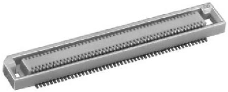
![3D rendering of a gray rectangular electronic component with multiple pins and a central port (no text or symbols visible)](.etx-im266-50-1j006-1010-212/a07cf6fb8365976ce44dce5d1146e3e610fdc750d761e4f4af829ed89c21136b.jpg)

# FX8C-100S-SV5

100-pin board-to-board connector for
9.5 mm board stacking

This connector can be used with :

- 9.5 mm through-hole standoffs (SMT type)
- 9.5 mm threaded standoffs (DIP type)
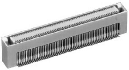
![3D rendering of a metallic rectangular electronic component with ribbed internal structure (no text or symbols)](.etx-im266-50-1j006-1010-212/fd13530b77a757f0f1eeb65b4b72b9d597b6deae43d1cac452a406b8c144d12a.jpg)

# FX8C/FX8 Common Spec

▶ Current capacity 0.4 A per pin
▶ Rated voltage 100 V AC
▶ Insulation resistance 100 M or greater @ 250 V DC
▶ Withstand voltage 300 V AC r.m.s.
▶ Contact resistance 45 m or less @ 100 mA DC
▶ Insulation PPS resin (Light brown, UL94V-0)
Contacts phosphor bronze (gold plated contacts and leads)

# A.2 Heatspreader Introduction

The heatspreader function is to ensure an identical mechanical profile for every ETX module. In this way the heat solution, that is built on top of the heatspreader is compatible with any ETX module not just the ETX-IM266 (or ETX-IM333).
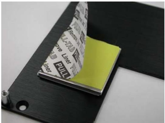
![Close-up of a metal sheet being extruded with a yellow adhesive tape, placed on a black surface (no text or symbols visible)](.etx-im266-50-1j006-1010-212/fe95e1b0408b54893326bc3187490c1570af43f8400d78c0f31bbb6cd62f967e.jpg)

Remove the protective layer from CPU and Northbridge pads before placing the heatspreader on the module.
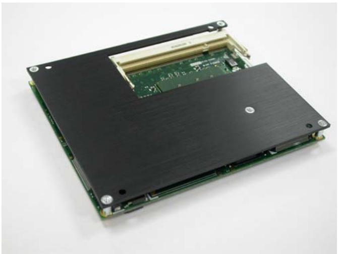
![Black and white photo of a computer motherboard with visible circuit board and connectors (no text or symbols)](.etx-im266-50-1j006-1010-212/814aa4a3c27224652d4882b08b5e878f3808d944513f45a7100c2527d2c1eaf9.jpg)

Heatspreader placed on ETX-IM266 (ETX-IM333) with free space to mount SODIMM memory
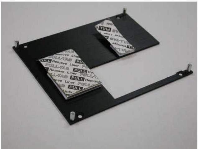
![FULL-TAB\nPULL Remove Liner PULL\nFULL-TAB PULL R0.\nPULL Remove Liner PULL\nFULL-TAB PULL Remove\nPULL Remove Liner PULL\nPULL R0.1\nPULL R0.2\nPULL R0.3](.etx-im266-50-1j006-1010-212/3c3559f16bd80a98d256a0570394ab9e7b715867cc4af9cefc169e50083590e0.jpg)

Heatpads for BGA type CPU's and Northbridge
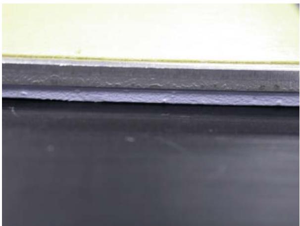
![Close-up of a dark surface with a horizontal white stripe and a yellow top layer (no text or symbols visible)](.etx-im266-50-1j006-1010-212/ca9eedb723f055453cd6f638cf2e6faf55f7ac5574012368bf7b918eb4814891.jpg)

# From top to bottom:

- Face change (yellow)
- Aluminum pad (silver)
- Flexible heat pad (light blue)
- Aluminum heatspreader plate (black)

# A.3 Mounting procedures

There are several standard ways to mount an ETX board with heatspreader on a carrier board. ETX boards may be mounted with 9 mm ETX connectors on the carrier board or standard 3 mm connectors. Mounting may also choose between two different types of heatspreaders, threaded standoffs which require inserting screws from under the carrier; or TOP mounting using through hole heatspreader standoffs and the carrier board standoffs are thread.

Top Mounting
3 mm Hirose FX8-100S-SV
Carrier Board Connectors
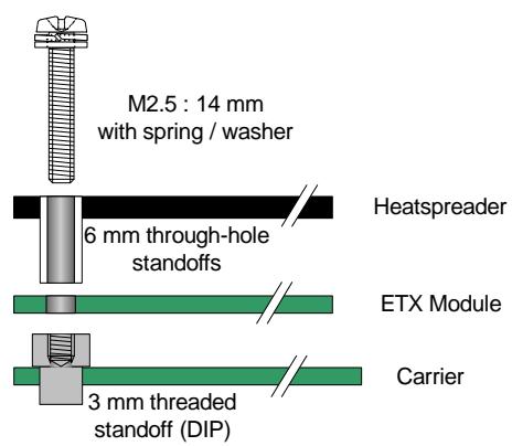
![M2.5 : 14 mm\nwith spring / washer\n6 mm through-hole\nstandoffs\nHeatspreader\nETX Module\n3 mm threaded\nstandoff (DIP)](.etx-im266-50-1j006-1010-212/3dcc47d0a8083a627a9b4f69190fc5600f0eb82d84cc5593d14e2f89f23422b6.jpg)

Bottom Mounting
3 mm Hirose FX8-100S-SV
Carrier Board Connectors
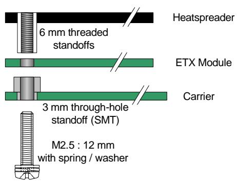
![Heatspreader\n6 mm threaded\nstandoffs\nETX Module\n3 mm through-hole\nstandoff (SMT)\nCarrier\nM2.5 : 12 mm\nwith spring / washer](.etx-im266-50-1j006-1010-212/48e16e779c668f0b676855ee5c91f142180de20b78ba870eda408d6cc1ff773d.jpg)

Top Mounting
9 mm Hirose FX8C-100S-SV5
Carrier Board Connectors
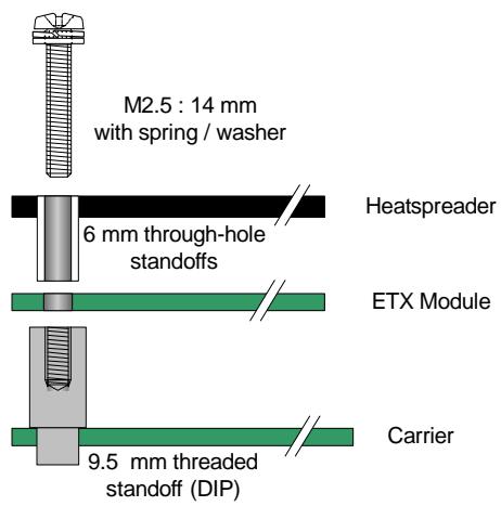
![M2.5 : 14 mm\nwith spring / washer\n6 mm through-hole\nstandoffs\nHeatspreader\nETX Module\n9.5 mm threaded\nstandoff (DIP)](.etx-im266-50-1j006-1010-212/35a121cf1fd112018e205c98c56f198b39309360052a5f5a4e0dcbe6e039bf04.jpg)

Bottom Mounting
9 mm Hirose FX8C-100S-SV5
Carrier Board Connectors
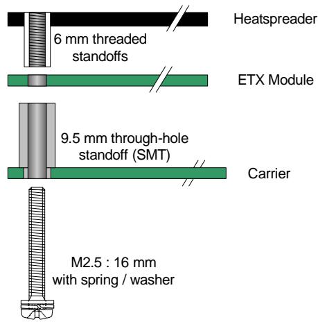
![Heatspreader\n6 mm threaded\nstandoffs\nETX Module\n9.5 mm through-hole\nstandoff (SMT)\nCarrier\nM2.5 : 16 mm\nwith spring / washer](.etx-im266-50-1j006-1010-212/ef3a8f561a479581c104b92e5668ef193f8ef7ad30e1fd05254f2bebad8ab64c.jpg)

# A.4 Standoff types

For different mounting procedures there are different, readily available standoffs. Note that threaded standoffs are all DIP type and the through-hole types are all SMT type. Other types not listed can be made available upon request.

<table><tr><td>33-72000-0030&lt;img src="images/d257affa8541947d397988465cafa096d11c6125c0c638e7c5a72df8463cff91.jpg"/&gt;</td><td>3 mm through-hole standoff (SMT type)for HTS-IM333 with 3 mm Hirose carrierboard connectors</td></tr><tr><td>33-72011-0030&lt;img src="images/347dd50a2f482cf1167e1b07326a10311e50da786193ea642478e47533ee84e0.jpg"/&gt;</td><td>3 mm threaded standoff (DIP type)for HTS-IM333-T with 3 mm Hirose carrierboard connectors</td></tr><tr><td>33-72007-9P50&lt;img src="images/15eb869318da7639bed93c6807e8f155e33f2f8f6ca5d229d47277e2e7e8411f.jpg"/&gt;</td><td>9.5 mm through-hole standoff (SMT type)for HTS-IM333 with 9 mm Hirosecarrier board connectors</td></tr><tr><td>33-72011-9P50&lt;img src="images/4f063a98b3ce760e094521ae28f638054294e31f14f00cd610e0592b1f9c7d2e.jpg"/&gt;</td><td>9.5 mm threaded standoff (DIP type)for HTS-IM333-T with 9 mm Hirosecarrier board connectors</td></tr></table>

A.5 Heatspreader Dimensions for HTS-IM333-B (threaded standoffs)
![| Component | Dimension (mm) |\n| :--- | :--- |\n| M2.5 H6-5X | 3780 |\n| Ø3.0 (Ø118) | 3661 |\n| Ø5.3 (Ø209) | 53 |\n| 96 (3780) | 3780 |\n| 93 (3661) | 3661 |\n| 71.5 (2815) | 2815 |\n| 57.4 (2260) | 2260 |\n| 43.4 (1709) | 1709 |\n| 6.65 (262) | 262 |\n| 6 (236) | 236 |\n| 4 (157) | 157 |\n| 3 (118) | 118 |\n| 0 (0) | 0 |\n| 0 (0) | 0 |\n| 3 (118) | 118 |\n| 7.35 (289) | 289 |\n| 10 (394) | 394 |\n| 12.65 (498) | 498 |\n| 29.4 (1157) | 1157 |\n| 30.5 (1201) | 1201 |\n| 44.5 (1752) | 1752 |\n| 73.3 (2886) | 2886 |\n| 76.8 (3024) | 3024 |\n| 106.8 (4205) | 4205 |\n| 111 (4370) | 4370 |\n| 114 (4488) | 4488 |\n| 51 (2008) | 2008 |\n| 30 (1181) | 1181 |\n| 21 (827) | 827 |\n| 8.5 (335) | 335 |\n| 3 (118) | 118 |\n| 2 (79) | 79 |\n| 0 (0) | 0 |\n| 6 (236) | 236 |\n| Aluminum Face change: Aluminium\nT-FLEX Aluminium Face change: Aluminium\nAluminium Face change: Aluminium Face change: Aluminium\nM2.5 H6-5X\nM2.5 H6-5X\nM2.5 H6-5X\nM2.5 H6-5X\nM2.5 H6-5X\nM2.5 H6-5X\nM2.5 H6-5X\nM2.5 H6-5X\nM2.5 H6-5X\nM2.5 H6-5X\nM2.5 H6-5x\nM2.5 H6-5x\nM2.5 H6-5x\nM2.5 H6-5x\nM2.5 H6-5x\nM2.5 H6-5x\nM2.5 H6-5x\nM2.5 H6-5x\nM2.5 H6-5x\nM2.5 H6-5x\nM2.5 H6-5m\nM2.5 H6-5m\nM2.5 H6-5m\nM2.5 H6-5m\nM2.5 H6-5m\nM2.5 H6-5m\nM2.5 H6-5m\nM2.5 H6-5m\nM2.5 H6-5m\nM2.5 H6-5m\nM2.5 H6-5n\nM2.5 H6-5n\nM2.5 H6-5n\nM2.5 H6-5n\nM2.5 H6-5n\nM2.5 H6-5n\nM2.5 H6-5n\nM2.5 H6-5n\nM2.5 H6-5n\nM2.5 H6-5n\nM2.5 H6-5m\nM2.5 H6-5m\nM2.5 H6-5m\nM2.5 H6-5m\nM2.5 H6-5m\nM2.5 H6-5m\nM2.5 H6-5m\nM2.5 H6-5m\nM2.5 H6-5m\nM2.5 H6-5nm\nM2.5 H6-5nm\nM2.5 H6-5nm\nM2.5 H6-5nm\nM2.5 H6-5nm\nM2.5 H6-5nm\nM2.5 H6-5nm\nM2.5 H6-5nm\nM2.5 H6-5nm\nM2.5 H6-5nm\nM2.5 H6-5m\nM2.5 H6-5m\nM2.5 H6-5m\nM2.5 H6-5m\nM2.5 H6-5m\nM2.5 H6-5m\nM2.5 H6-5m\nM2.5 H6-5m\nM2.5 H6-5m\nM2.5 H6-5mm\nM2.5 H6-5mm\nM2.5 H6-5mm\nM2.5 H6-5mm\nM2.5 H6-5mm\nM2.5 H6-5mm\nM2.5 H6-5mm\nM2.5 H6-5mm\nM2.5 H6-5mm\nM2.5 H6-5mm\nM2.5 H6-5m\nM2.5 H6-5m\nM2.5 H6-5m\nM2.5 H6-5m\nM2.5 H6-5m\nM2.5 H6-5m\nM2.5 H6-5m\nM2.5 H6-5m\nM2.5 H6-5m\nM2.5 H6-5cm\nM2.5 H6-5cm\nM2.5 H6-5cm\nM2.5 H6-5cm\nM2.5 H6-5cm\nM2.5 H6-5cm\nM2.5 H6-5cm\nM2.5 H6-5cm\nM2.5 H6-5cm\nM2.5 H6-4mm\nM2.49 mm (with label 'These parts on the rear side.')](.etx-im266-50-1j006-1010-212/59686450858d8ecf8884427e59dd5a7e3c26d6e52c32255c8897482d63ee8832.jpg)

The heatspreader comes included with four M2.5 at 12 mm with washer/spacer
The above heatspreader can be used with ETX-IM266 and ETX-IM333 models.

A.6 Heatspreader Dimensions for HTS-IM333-BT (through-hole standoffs)
![This is an icon depicting a white sheet of paper with a folded top-right corner, featuring a large red checkmark in the center. Below the paper graphic, the text 'NOTE:' appears in black capital letters.](.etx-im266-50-1j006-1010-212/8dccb3f08cd1fe12e539468a34d905d6180d35685f1f8ab4122d422c2bf8ae2d.jpg)
Only for BGA type LV and ULV PU's below 15 Watts

![| Dimension | Value     |\n| --------- | --------- |\n| 0         | 0         |\n| 3         | 118       |\n| 7.35      | 289       |\n| 10        | 394       |\n| 12.65     | 498       |\n| 29.4      | 1157      |\n| 30.5      | 1201      |\n| 44.5      | 1752      |\n| 73.3      | 2886      |\n| 76.8      | 3024      |\n| 106.8     | 4205      |\n| 111       | 4370      |\n| 114       | 4488      |\n| 3         | 118       |\n| 6         | 236       |\n| 4         | 157       |\n| 3         | 118       |\n| 6.65      | 262       |\n| 71.5      | 2815      |\n| 57.4      | 2260      |\n| 43.4      | 1709      |\n| 14        | 551       |\n| 14        | 551       |\n| 30        | 1181      |\n| 51        | 2008      |\n| 30        | 1181      |\n| Ø2.5      | Ø98       |\n| Ø4.0      | Ø157      |\n| Ø3.0      | Ø118      |\n| Ø5.3      | Ø209      |](.etx-im266-50-1j006-1010-212/fb3ed3aef72d5b8cfdcf966b8fdbc9209749d8bec05221319c7af566bcbd1704.jpg)

![2 (79)\n0 (0)\n6 (236)\nT-FLEX\nAluminium\nFace change\nAluminium\n1.75 (69)\n2 (79)\n0.1 (4)\nT-FLEX\nAluminium\nFace change\n1.5 (59)\n2 (79)\n0.1 (4)](.etx-im266-50-1j006-1010-212/f556577edb0fe8ba72666251480cdb2b766ac4254f918ff06fdc01023dca989e.jpg)

The heatspreader comes included with four M2.5 at 14 mm with washer/spacer, If using 9 mm standoffs on the carrier board, M2.5 at 18 mm with washer/spring are required and must be ordered separately.
The above heatspreader can be used with ETX-IM266 and ETX-IM333 models.

# A.7 THSF-IM333: High Performance Heatsink with Fan

The THSF-IM333-S (socket type CPU) and THSF-IM333-B (BGA, soldered type CPU) are high performance heatsinks that can easily support CPU types with thermal outputs of up to 35 Watts. The fan on the heatsink requires a 12 Volt power source.

The THSF-IM333 only supports "bottom mounting" and can be used with either ETX-IM266 or with ETX-IM333 models which are mechanically identical.

![Close-up of a heat sink with a black CPU fan and copper cooling element, no visible text or symbols](.etx-im266-50-1j006-1010-212/6242b5ca9f7c200b85624b6e8c839359e42e8716d4c9ba9e67595637fc914abb.jpg)

Aluminum body, with copper CPU head and 12 V high performance fan

![Green computer motherboard with CPU socket, RAM slots, and various connectors (no visible text or labels)](.etx-im266-50-1j006-1010-212/b19c4609ffcb23ca89c966f7602d13790129b04f65b37840cad9e4448a2ce8bb.jpg)

THSF-IM333 installed on ETX-IM266 and ETX-carrier board.

# A.8 THS-IM333 Series: Low Profile Heatsinks

The THS-IM333 Heatsink Series (for BGA type CPUs only) are low profile heatsinks that are optimized for reduced height applications. Although the heatsinks are fanless they still require some airflow to efficiently cool applications. The heatsinks are available in two cooling fin orientations and have both top and bottom mounting options (threaded- vs through-hole standoffs. THS-IM333 Series can be used with either ETX-IM266 and ETX-IM333 models which are mechanically identical.

![Two electronic components: a green circuit board and a metallic heat sink, placed on a wooden surface (no text or symbols visible)](.etx-im266-50-1j006-1010-212/86ad27b83b621b4abbf649fc7ca2d95d4f5104fc274a51c0304c51c6b4f9d54f.jpg)

THSF-IM333-T heatsink with ETX-IM333-P1400

![Close-up of a metallic electronic component with multiple square cutouts and mounting holes, placed on a wooden surface (no visible text or symbols)](.etx-im266-50-1j006-1010-212/10e9c76d7bd85fbdefe94eca6930b1410540b87be14df762572c484f58b6f964.jpg)

Pads for CPU and Northbridge

![Close-up of a computer processor cooling module on a wooden surface (no text or symbols visible)](.etx-im266-50-1j006-1010-212/20d2d733ab743c5e4f4539eb78bdcd5d27e23e3054618da4a638308066ecb0ed.jpg)

Heatsink mounted on ETX-IM266

# A.9 Dimensions for THS-IM333 Series

THS-IM333
Heatsink with short fins and threaded standoffs for bottom mounting
![Ø4.0 / M2.5\nx6 pcs\n114.0\n26.4\n108.0\n45.9\n21.5\n95.0\n90.0\n2.5\n3.0\n4.0\n3.0\n4.0\n7.0\n2.5\n2.0\n2.0\nM2.5 H6 standoffs x6\n3.7\n8.0](.etx-im266-50-1j006-1010-212/b42ddd2606b36238ae7e1fd09befdc465fd6445fbcd9bb48f280ad4b11a1e2b5.jpg)

THS-IM333-L
Heatsink with long fins and threaded standoffs for bottom mounting
![Ø4.0 / M2.5\nx6 pcs\n114.0\n108.0\n26.4\n45.9\n21.5\n95.0\n90.0\n2.5\n3.0\n4.0\n3.0\n4.0\n7.0\n2.5\n2.0\n2.0\nM2.5 H6 standoffs x6\n3.7\n8.0](.etx-im266-50-1j006-1010-212/8efe4bea94e99acae79196849757489afc494b6b52acf6adf490f3af15d82837.jpg)

THS-IM333-T
Heatsink with short fins and through-hole standoffs for top mounting
![Ø4.0 / Ø2.5\nx4 pcs\n114.0\n26.4\n108.0\n45.9\n21.5\n95.0\n90.0\n2.5\n3.0\n4.0\n3.0\n4.0\n7.0\n2.5\n2.0\nThroughhole standoffs x4\nØ4.0 external\nØ2.5 internal\nM2.5 H6\nstandoffs x2\n3.7\n8.0](.etx-im266-50-1j006-1010-212/44b9ebb4091c6463f802017305dafc6ae3bc3eca4cda698df52036186bd2d344.jpg)

THS-IM333-TL
Heatsink with long fins and and through-hole standoffs for top mounting
![Ø4.0 / Ø2.5\nx4 pcs\n114.0\n26.4\n108.0\n45.9\n21.5\n95.0\n90.0\n2.5\n3.0\n4.0\n3.0\n4.0\n7.0\n2.5\n2.0\nThroughhole standoffs x4\nØ4.0 external\nØ2.5 internal\nM2.5 H6\nstandoffs x2\n3.7\n8.0](.etx-im266-50-1j006-1010-212/fb0fe50ae5b5db72e3c98311bbe1588069554456a33b01506822f1745afa2efc.jpg)

This page intentionally left blank.

# Important Safety Instructions

For user safety, please read and follow all instructions, warnings, cautions, and notes marked in this manual and on the associated equipment before handling/operating the equipment.

▶ Read these safety instructions carefully.
- Keep this user's manual for future reference.
Read the specifications section of this manual for detailed information on the operating environment of this equipment.
When installing/mounting or uninstalling/removing equipment:

\- Turn off power and unplug any power cords/cables.

▶ To avoid electrical shock and/or damage to equipment:

- Keep equipment away from water or liquid sources;
- Keep equipment away from high heat or high humidity;
- Keep equipment properly ventilated (do not block or cover ventilation openings);
- Make sure to use recommended voltage and power source settings;
- Always install and operate equipment near an easily accessible electrical socket-outlet;
- Secure the power cord (do not place any object on/over the power cord);
- Only install/attach and operate equipment on stable surfaces and/or recommended mountings; and,
- If the equipment will not be used for long periods of time, turn off and unplug the equipment from its power source.

▶ Never attempt to fix the equipment. Equipment should only be serviced by qualified personnel.
▶ A Lithium-type battery may be provided for uninterrupted, backup or emergency power.

![The image shows a yellow triangular warning sign with a black border. Inside the triangle is a black exclamation point. Below the triangle, the text 'CAUTION:' is printed in black capital letters.](.etx-im266-50-1j006-1010-212/fc6937eb5414e199b3bd49435c6b8cac3688d0dbcc75fab7bbbb552c8127a0e1.jpg)

Risk of explosion if battery is replaced by an incorrect type. Dispose of used batteries according to the instructions.

▶ Equipment must be serviced by authorized technicians when:

- The power cord or plug is damaged;
- Liquid has penetrated the equipment;
- It has been exposed to high humidity/moisture;
- It is not functioning or does not function according to the user's manual;
- It has been dropped and/or damaged; and/or,
- It has an obvious sign of breakage.

# Getting Service

Contact us should you require any service or assistance.

# ADLINK Technology Inc. (Headquarters)

Web Site: http://www.adlinktech.com

Sales & Service: service@adlinktech.com

Telephone No.: +886-2-8226-5877

Fax No.: +886-2-8226-5717

Mailing Address: 9F No. 166 Jian Yi Road, Chungho City, Taipei 235, Taiwan

# ADLINK Technology America Inc.

Sales & Service: info@adlinktech.com

Toll-Free: +1-866-4 ADLINK

Fax No.: +1-949-727-2099

Mailing Address: 8900 Research Drive,

Irvine, CA 92618, USA

# ADLINK Technology Co. Ltd. (Beijing)

Sales & Service: market@adlinktech.com

Telephone No.: +86-10-5885-8666

Fax No.: +86-10-5885-8625

Mailing Address: Rm. 801, Power Creative E, No. 1, B/D Shang Di East Rd.

Beijing, 100085 China

# ADLINK Technology Co. Ltd. (Shanghai)

Sales & Service: market@adlinktech.com

Telephone No.: +86-21-6495-5210

Fax No.: +86-21-5450-0414

Mailing Address: 4F, Bldg. 39, No.333 Qinjiang Road, Cao He Jing High-Tech Park

Shanghai, 200233 China

# ADLINK Technology Co. Ltd. (Shenzhen)

Sales & Service: market@adlinktech.com

Telephone No.: +86-755-2643-4858

Fax No.: +86-755-2664-6353

Mailing Address: 2F, C Block, Bld. A1, Cyber-Tech Zone, Gao Xin Ave. Sec 7,

High-Tech Industrial Park S., Shenzhen, 518054 China

# ADLINK Technology Inc. (European Liaison Office)

Sales & Service: emea@adlinktech.com

Telephone No.: +49-211-495-5552

Fax No.: +49-211-495-5557

Mailing Address: Nord Carree 3, 40477

Düsseldorf, Germany

# ADLINK Technology Japan Corp.

Sales & Service: japan@adlinktech.com

Telephone No.: +81-3-4455-3722

Fax No.: +81-3-5333-6040

Mailing Address: Asahiseimei Hatagaya Bld. 8Fl. 1-1-2

Hatagaya Shibuya-ku, Tokyo, Japan

# ADLINK Technology Inc. (South Korea Liaison Office)

Sales & Service: korea@adlinktech.com

Telephone No.: +82-2-2057-0565

Fax No.: +82-2-2057-0563

Mailing Address: #402, Dongsung B/D, 60-12, Nonhyeon-dong Gangnam-gu,

Seoul, 135-010, South Korea

# ADLINK Technology Singapore Pte. Ltd.

Sales & Service: singapore@adlinktech.com

Telephone No.: +65-6844-2261

Fax No.: +65-6844-2263

Mailing Address: 84 Genting Lane #07-02A, Cityneon Design Center,

Singapore 349584

# ADLINK Technology Singapore Pte. Ltd. (India Liaison Office)

Sales & Service: india@adlinktech.com

Telephone No.: +91-80-6560-5817

Fax No.: +91-80-2244-3548

Mailing Address: No. 1357, Ground Floor, "Anupama", Aurobindo Marg JP Nagar (Ph-1)

Bangalor, Karnataka 560078, India

![The image displays a black circle containing the white universal recycling symbol. The symbol consists of three arrows arranged in a triangular loop, where each arrow features three horizontal stripes on its upper section. There is no text visible in the image.](.etx-im266-50-1j006-1010-212/985d5cc8ba4ad8e817f6b7aa323b4e4c0f09e8f705b3bdc42614cdcfb671979d.jpg)
[🔗 Link to the original document](.etx-im266-50-1j006-1010-212/etx-im266-50-1j006-1010-212.pdf)
