# Express-CBR

# (Computer On Module)

# Reference Manual

P/N 50-1Z040-1020

# DISCLAIMER

ADLINK Technology, Incorporated makes no representations or warranties with respect to the contents of this manual or of the associated ADLINK products, and specifically disclaims any implied warranties of merchantability or fitness for any particular purpose. ADLINK shall under no circumstances be liable for incidental or consequential damages or related expenses resulting from the use of this product, even if it has been notified of the possibility of such damages. ADLINK reserves the right to revise this publication from time to time without obligation to notify any person of such revisions. If errors are found, please contact ADLINK at the address listed on this Notice Page.

# TRADEMARKS

CoreModule and the Ampro logo are registered trademarks, and ADLINK, Little Board, LittleBoard, MightyBoard, MightySystem, MilSystem, MiniModule, ReadyBoard, ReadyBox, ReadyPanel, RuffSystem, and ReadySystem are trademarks of ADLINK Technology, Inc. All other marks are the property of their respective companies.

REVISION HISTORY

<table><tr><td>Revision</td><td>Reason for Change</td><td>Date</td></tr><tr><td>1000</td><td>Initial Release</td><td>June/10</td></tr><tr><td>1010</td><td>Updated PU/PD info in COM Express pinout tables; added BIOS Setup Menus section to Chapter 4</td><td>Feb/11</td></tr><tr><td>1.02</td><td>Added Running Time initialization procedure to “BIOS Main Setup Screen” on page 35; changed revision of this document from 1010 to 1.02 in compliance with converting the revision scheme from Ampro to ADLINK</td><td>Sept/15</td></tr><tr><td></td><td></td><td></td></tr><tr><td></td><td></td><td></td></tr><tr><td></td><td></td><td></td></tr><tr><td></td><td></td><td></td></tr></table>

ADLINK Technology, Incorporated

5215 Hellyer Avenue, #110

San Jose, CA 95138-1007

Tel. 408 360-0200

Fax 408 360-0222

www.adlinktech.com

© Copyright 2010, 2011, 2012, 2013, 2014, 2015 ADLINK Technology, Incorporated

# Audience

This manual provides reference only for computer design engineers, including but not limited to hardware and software designers and applications engineers. ADLINK Technology, Inc. assumes you are qualified to design and implement prototype computer equipment.

# Contents

# Chapter 1 About This Manual ..

Purpose of this Manual ..

References

# Chapter 2 Product Overview...........

COM Express Concept .. .3

COM Express Architecture . .4

Product Description.. 4

Module Features .5

Block Diagram . .7

Major Components (ICs)..... .8

Connectors and Sockets.... .....10

Specifications......... ..12

Physical Specifications ..... ..12

Power Specifications ....... ..13

Environmental Specifications...... ...15

Thermal/Cooling Requirements.. ...15

Mechanical Specifications ...... ..17

# Chapter 3 Hardware . .19

Overview .... ...19

Interrupt Channel Assignments .20

Memory Map . ..21

I/O Address Map . ..22

COM Express A-B Connector... ..23

LPC Interface ........ .23

SATA Interface . .23

USB Interface . .24

Power Interface . .24

Power Management.. ..24

Video Interfaces..... .24

VGA .... ..24

LVDS .. ..24

Audio Interface ..... .24

Ethernet Interface ..... .24

I²C™ Bus . .24

PCI Express™ .25

ExpressCard™ . ..25

System Management Bus (SMBus) .25

GPIO. .25

COM Express C-D Connector ..28

IDE Interface.. .28

PCI Interface.. .28

PCI Express Graphics (PEG) . ..28

SDVO.. .29

Watchdog Timer... ..32

TPM (Trusted Platform Module [Optional]) . ..32

CPU Temperature Monitor........... ..32

# Chapter 4 BIOS Setup ..... . 33

Introduction... .. 33

Entering BIOS Setup (VGA Display) .. . 33

OEM Logo Utility (Splash Screen).. . 33

Logo Image Requirements.. . 33

BIOS Setup Menus .. . 34

BIOS Main Setup Screen .. . 35

BIOS Advanced Setup Screen... . 36

BIOS Chipset Setup Screen.. . 41

BIOS Boot Setup Screen .. . 43

BIOS Security Setup Screen.. . 44

BIOS Save & Exit Setup Screen ...... .. 45

# Appendix A Technical Support .. . 47

# Purpose of this Manual

This manual is for designers of systems based on the Express-CBR (Computer On Module). This manual contains information that permits designers to create an embedded system based on specific design requirements.

Information provided in this reference manual includes:

Express-CBR specifications
Environmental requirements
Major ICs and features implemented
Express-CBR connector/pin numbers and definitions
• BIOS Setup information

Information not provided in this reference manual includes:

• Detailed chip specifications
• Internal component operation
• Internal registers or signal operations
Bus or signal timing for industry standard busses and signals
• Pinout definitions for industry standard interfaces

# References

The following list of references may be helpful for you to complete your custom design successfully.

# Specifications

COM Express Specification Revision 1.0 Web site: http://www.picmg.org/

PCI Specification Revision 2.3 Web site: http://www.pcisig.com

PCIe Specification Revision 1.1 Web site: http://www.pcisig.com/specifications/pciexpress/base

# Chip Specifications

Intel Corporation and the Core™ i7 -600 series CPU, used for the integrated processor core and graphics memory hub
Web site: http://www.intel.com/products/processor/corei7/mobile/techdocs.htm

Intel Corporation and the BD82QM57 chip, used for the Platform Controller Hub Datasheet: http://www.intel.com/Assets/PDF/datasheet/322169.pdf = PCH

Intel Corporation and the 82574IT chip used for the Gigabit Ethernet controller Datasheet: http://download.intel.com/design/network/datashts/82574.pdf

NOTE If you are unable to locate the datasheets using the links provided, go to the manufacturer’s web site where you can perform a search using the chip datasheet number or name listed, including the extension (htm for web page, pdf for file name, etc.)

This introduction presents general information about the COM Express™ architecture and the Express-CBR Computer-On-Module (COM). After reading this chapter you should understand:

• COM Express concept
COM Express architecture
Express-CBR features
Express-CBR functional block diagram
Express-CBR major components
Express-CBR connectors
Express-CBR specifications

# COM Express Concept

COM Express is an open industry standard defined specifically for COMs (Computer On Modules). Its creation provides the ability to make a smooth transition from legacy parallel interfaces to the newest technologies based on serial buses available today. COM Express modules are available in the following form factors:

Compact 95mm x 95mm
Basic 125mm x 95mm
Extended 155mm x 110mm

The COM Express specification 1.0 defines five different pinout types.

Table 2-1. COM Express Pinout Types

<table><tr><td>Types</td><td>Connector Rows</td><td>PCI Express Lanes</td><td>PCI</td><td>IDE Channels</td><td>LAN ports</td></tr><tr><td>Type 1</td><td>A-B</td><td>Up to 6</td><td></td><td></td><td>1</td></tr><tr><td>Type 2</td><td>A-B C-D</td><td>Up to 22</td><td>32 bit</td><td>1</td><td>1</td></tr><tr><td>Type 3</td><td>A-B C-D</td><td>Up to 22</td><td>32 bit</td><td></td><td>3</td></tr><tr><td>Type 4</td><td>A-B C-D</td><td>Up to 32</td><td></td><td>1</td><td>1</td></tr><tr><td>Type 5</td><td>A-B C-D</td><td>Up to 32</td><td></td><td></td><td>3</td></tr></table>

The Express-CBR utilizes the Type 2 pinout definition, equipped with two high performance connectors that ensure stable data throughput.

The COM (Computer On Module) integrates all the core components and is mounted onto an application specific baseboard. COM modules are legacy-free designs (no Super I/O, PS/2 keyboard, and PS/2 mouse) and provide most of the functional requirements for any application. These functions include, but are not limited to a rich complement of contemporary, high bandwidth serial interfaces such as PCI Express, Serial ATA, USB 2.0, and Gigabit Ethernet. The Type 2 pinout provides the ability to offer 32-bit PCI, Parallel ATA, and LPC options thereby expanding the range of potential peripherals. The robust thermal and mechanical concept, combined with extended power management capabilities, is perfectly suited for all applications.

Baseboard designers can utilize as little or as many of the I/O interfaces as necessary. The baseboard can therefore provide all the interface connectors required to attach the system to the application specific peripherals. This versatility allows the designer to create a dense and optimized package, which results in a more reliable product while simplifying system integration. Most importantly, COM Express modules are scalable, which means once an application has been created there is the ability to diversify the product range through the use of different performance class or form factor modules. Simply unplug one module and replace it with another. No redesign is necessary.

# COM Express Architecture

The COM Express specification was developed by the PCI Industrial Computer Manufacturing Group (PICMG) in close collaboration with many leading companies across the embedded industry in order to find an implementation solution to handle upcoming new high speed serial I/Os, processors, and chipsets. COM Express specifies three form factors, as well as five different types of connector pinouts.

The three form factors are referred to as Compact, Basic, and Extended. The Compact form factor is 95mm x 95mm designed to match the requirements of small applications. The Basic module footprint is 125mm x 95mm and focuses on space-constrained, low power systems which typically do not contain more than one horizontal mounted SODIMM. The Extended footprint is slightly larger at 155mm x 110mm and supports up to two full-size, vertically mounted DIMM modules to accommodate larger memory configurations for high-performance CPUs, chipsets and multiprocessor systems. The placement of the shielded 220-pin connectors and the mounting holes are identical between these three footprints.

![155\n151\n95\n91\n95\n91\n91\nCompact Module\nBasic Module\n70\n106\n110\nLegend 'mounting holes'\nCompact Module\nExtended Module\nBasic Module (ΔΔ Basic + Compact Module)\nAll 3 Modules](.express-cbr-50-1z040-1020-102-en/868c07f9d30d9a9c26e3e38fc7f0885273c0a8c2f88b5b3b98b832e21f86705e.jpg)

Figure 2-1. Compact, Basic and Extended Form Factors

# Product Description

The Express-CBR is an exceptionally high integration, high performance, rugged Intel Core™ i7 processor based system compatible with the COM Express standard. This rugged and high quality module system contains all the component subsystems of an ATX motherboard.

The Intel Core i7 incorporates a dual processor core with an integrated Graphics and Memory Hub (GMH), providing a low-power, high-performance processor, a memory controller for up to 8GB of SODIMM memory, and a graphics controller for LVDS, VGA, and PCI Express graphics (PEG) signals.

The Intel BD82QM57 chipset provides controllers for the Platform Controller Hub (PCH) featuring eight USB ports, four SATA ports, eight GPIO ports, one Ultra DMA 33/66/100 IDE controller supporting two IDE drives, and one Gigabit Ethernet interface (external magnetics required).

Expansion for additional system functions is possible on the Express-CBR through the PCI, PCIe, and LPC expansion buses. The PCI bus operates at a clock speed of 33MHz.

The Express-CBR is particularly well suited to either embedded or portable applications and meets the size, power consumption, temperature range, quality, and reliability demands of embedded system applications.

# Module Features

# CPU

Intel 1.06GHz or 2.0GHz LV, Core i7 -600 series processor
 DMI (Direct Media Interface) with 1 GB/s of bandwidth in each direction
Internal 4MB L2 cache
 Enhanced Intel SpeedStep® Technology (EIST)

# • Memory

Two standard 204-pin DDR3 SODIMM sockets
Supports +1.5V DDR3, 800/1066MHz RAM up to 8 GB total
Supports non-ECC, unbuffered memory

# . Interface Buses

 PCI between PCH and COM Express A-B connector
 PCIe between PCH and COM Express C-D connector
DMI (Direct Media Interface) between processor and PCH
FDI (Flexible Display Interface) between graphics controller and PCH
 LPC (Low Pin Count) for LPC devices
 I 2 C for fast mode I2 C devices

# . COM Express Interface

 IDE Interface
Supports one enhanced IDE device
Supports single master mode
Supports Ultra DMA 100/66/33 in master mode
Supports ATAPI and DVD peripherals
Supports IDE native and ATA compatibility modes

# SATA Interface

Provides four SATA ports
Supports Native Command Queuing
Provides Auto Activate for DMA
Supports Hot Plug features

# HD Audio

Provides Intel HD Audio controller
Provides 32-bit sample depth
Supports sample rates up to 192kHz

# USB Port Interface

Supports two root USB hubs
Supports eight USB ports
Supports USB V2.0

 Ethernet Interface

Intel 82574IT Ethernet controller chip
Supports one Gigabit Ethernet port
Supports IEEE 802.3 compatible physical layer
Supports Auto-negotiation for speed, duplex mode, and flow control
Supports full-duplex or half-duplex modes
- Full-duplex mode supports transmit and receive frames simultaneously
- Supports IEEE 802.3x flow control in full duplex mode
- Half-duplex mode supports enhanced proprietary collision reduction mode

Video Interfaces (VGA/LVDS/PEG)

Support VGA (up to 2048 x 1536 bpp at 75Hz)
24-bit flat panel outputs (LVDS)
Digital Display Interface (SDVO B)
PCI Express Graphics (PEG) Interface

• Miscellaneous

Real Time Clock (RTC) with external replaceable battery
Watchdog Timer (WDT)
TPM (Trusted Platform Module) - Optional
CPU Temperature Monitor
 Logo Screen Utility (Splash)

# Block Diagram

Figure 2-2 shows the functional components of the module.
![Based on the provided block diagram, here are the labeled blocks and their connections:\n\n**Labeled Blocks:**\n*   **CPU:** CPU Intel Core i7 1.06 and 2.0 GHz (with integrated Processor Core and Graphics Memory Hub)\n*   **Memory:** DDR3 SODIMM Sockets (2)\n*   **South Bridge:** PCH Intel BD82QM57\n*   **Storage Controller:** SATA to PATA Controller JMicron JMD330\n*   **Network Controller:** Gigabit Ethernet Intel 82574IT\n*   **System Controller:** Board Controller\n*   **Storage:** SPI Flash\n*   **Security:** TPM - (Optional)\n*   **Connector A/B:** COM Express Connector - Rows A and B (containing blocks for: VBattery (RTC), X1 PCIe (6), SMBus, Gb Ethernet, HDA Link, USB 2.0 (8), I2C, 12V Input, SATA (4), LPC, GPIO (8), 5V Standby, LVDS (2), VGA, PWR Mgmt)\n*   **Connector C/D:** COM Express Connector - Rows C and D (containing blocks for: IDE, PCI, PEG, 12V Input)\n\n**Connections:**\n*   **CPU to Memory:**\n    *   'Channel - A' (labeled 800/1066MHz, 1.5V, 8GB Max.)\n    *   'Channel - B'\n*   **CPU to PCH:**\n    *   'DMI (4)' (bidirectional)\n    *   'FDI'\n*   **CPU to Connector C/D (PEG block):** 'PCIe Graphics, X8/eDP - PEG'\n*   **PCH to SPI Flash:** Bidirectional connection.\n*   **PCH to SATA to PATA Controller JMicron JMD330:** 'SATA (1)' (bidirectional)\n*   **PCH to Gigabit Ethernet Intel 82574IT:** 'X1 PCIe (1)' (bidirectional)\n*   **PCH to Connector C/D (PEG block):** 'SDVO B'\n*   **PCH to Connector C/D (PCI block):** 'PCI (32bit/33MHz)'\n*   **PCH to TPM - (Optional):** Arrow pointing up labeled 'TPM - (Optional)'.\n*   **PCH to Connector A/B:**\n    *   'LVDS' connects to LVDS (2)\n    *   'VGA' connects to VGA\n    *   'LPC' connects to LPC\n    *   'Intel - HDA Link' connects to HDA Link\n    *   'SATA (4)' connects to SATA (4)\n    *   'X1 PCIe (6)' connects to X1 PCIe (6)\n    *   'USB' connects to USB 2.0 (8)\n    *   'VBATT (RTC)' connects to VBattery (RTC)\n    *   'SMBus' connects to SMBus\n    *   'I2C' connects to Board Controller (bidirectional), which then connects to the I2C block in the connector.\n    *   'GPIO' connects to GPIO (8)\n    *   'PWR Management' connects to PWR Mgmt\n*   **SATA to PATA Controller JMicron JMD330 to Connector C/D (IDE block):** 'IDE'\n*   **Gigabit Ethernet Intel 82574IT to Connector A/B (Gb Ethernet block):** 'Gigabit Ethernet - MDI'](.express-cbr-50-1z040-1020-102-en/5ec70c4289da1876c738cfaf675a0c5dbd1ac0fac46ba46575deb3a0c9dc77a7.jpg)

Figure 2-2. Functional Block Diagram

# Major Components (ICs)

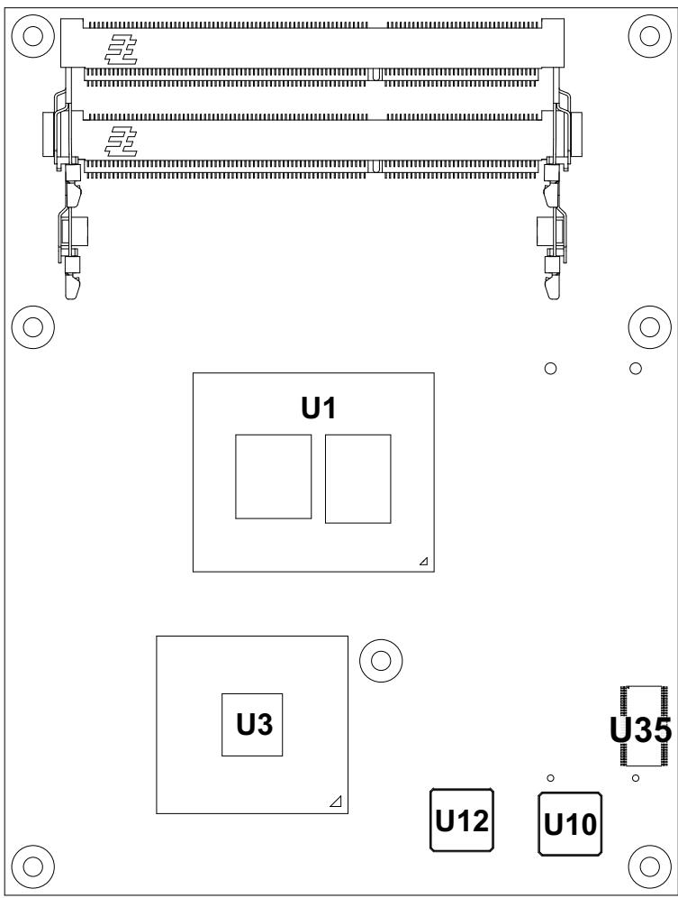
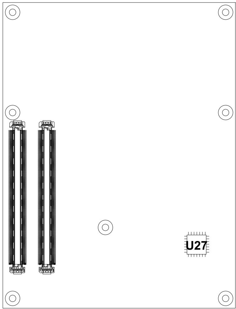
Table 2-2 lists the major integrated circuits on the Express-CBR, including a brief description of each IC. Figures 2-3 and 2-4 show the locations of the major ICs.

Table 2-2. Major Integrated Circuit Descriptions and Functions

<table><tr><td>Chip Type</td><td>Mfg.</td><td>Model</td><td>Description</td><td>Function</td></tr><tr><td>CPU (U1)</td><td>Intel</td><td>Core i7</td><td>1.06GHz and 2.0GHz512KB L2 cacheprocessors</td><td>Integrated CPU, memory, and video</td></tr><tr><td>PCH (Platform Controller Hub [U3])</td><td>Intel</td><td>BD82QM57 (PCH)</td><td>Southbridge I/O controller functions</td><td>I/O functions</td></tr><tr><td>Ethernet Controller (U10)</td><td>Intel</td><td>82574IT</td><td>Ethernet Controller – This chip provides Gigabit Ethernet function</td><td>Ethernet</td></tr><tr><td>SATA to PATA Controller (U12)</td><td>JMicron</td><td>JMD330APC1-QIBD</td><td>Provides function for converting SATA signals to PATA signals</td><td>Signal Conversion</td></tr><tr><td>TPM (Trusted Platform Module [U35]) - Optional</td><td>Infineon</td><td>SLB9635TT1.2</td><td>Provides security functionsCaution: Boards with the TPM option, feature only one temperature range from -20° to +70°C.</td><td>Security</td></tr><tr><td>Board Controller (U27)</td><td>Atmel</td><td>ATMEGA168V-10AU</td><td>Provides control for I2C, Watchdog Timer, and LVDS functions</td><td>Micro Controller</td></tr></table>

U1 - CPU
U3 - PCH
U10 - Ethernet Controller
U12 - SATA to PATA Controller
U35 - TPM [Optional]
![U1\nU3\nU12 U10\nU35](.express-cbr-50-1z040-1020-102-en/89c6fea0ff31dd9ff73995b3976458116b67aed0d73a2e55f26ef3d3d4ead14a.jpg)

Express-CBR\_comp\_top\_side\_a
Figure 2-3. Component Locations (Top Side)

Key: U27 - Board Controller
![Pure electrical circuit lines without any symbols](.express-cbr-50-1z040-1020-102-en/b209f6657e34d0338cae22b3037365497a1831a3d8e3da96b36a1dac2efc32e8.jpg)

Express-CBR\_comp\_bottom\_side\_a

Figure 2-4. Component Locations (Bottom Side)

# Connectors and Sockets

Table 2-3 describes the connectors and sockets shown in Figures 2-5 and 2-6.

Table 2-3. Module Connector and Socket Descriptions

<table><tr><td>Jack/Plug #</td><td>Board Access</td><td>Description</td></tr><tr><td>J5 – Memory</td><td>Top</td><td>204-pin socket for DDR3 SODIMM</td></tr><tr><td>J6 – Memory</td><td>Top</td><td>204-pin socket for DDR3 SODIMM</td></tr><tr><td>J4 – COM Express A-B (see Figure 2-6 on page 12.)</td><td>Bottom</td><td>220-pin connector for Northbridge Video and Southbridge I/O functions.</td></tr><tr><td>J4 – COM Express C-D (see Figure 2-6 on page 12.)</td><td>Bottom</td><td>220-pin connector for Northbridge Video and Southbridge I/O functions.</td></tr></table>

Key:

J5 - DDR3 SODIMM Socket

J6 - DDR3 SODIMM Socket

![J6\nJ5\nExpress-CBR conn_top_side_a](.express-cbr-50-1z040-1020-102-en/4fa9ac07528e4b8056a8fe9d911b2ed9edd36309a2cffd6f808474d02068e84b.jpg)

Figure 2-5. Connector Locations (Top Side)

![Key:\nJ4A - COM Express pins A1-A110\nJ4B - COM Express pins B1-B110\nJ4C - COM Express pins C1-C110\nJ4D - COM Express pins D1-D110\nJ4\nAB CD\nExpress-CBR conn_bottom_side_a](.express-cbr-50-1z040-1020-102-en/71368ec7569657f956ca547ac3a6db95a736e1369eeb065be6edfbea8cdb1137.jpg)

Figure 2-6. Connector Locations (Bottom Side)

# Specifications

# Physical Specifications

Table 2-4 lists the physical dimensions of the module.

Table 2-4. Weight and Footprint Dimensions

<table><tr><td>Item</td><td>Dimension</td><td rowspan="6">NOTE</td><td rowspan="6">Overall height is measured from the upper board surface to the highest permanent component on the upper board surface. This measurement does not include the cooling solution, which can vary. The cooling solution could increase this dimension.</td></tr><tr><td>Weight</td><td>0.09 kg (0.20 lb)</td></tr><tr><td>Height (overall)</td><td>9.20 mm (0.36 inches)</td></tr><tr><td>Board thickness</td><td>2.362 mm (0.093 inches)</td></tr><tr><td>Width</td><td>95.00 mm (3.74 inches)</td></tr><tr><td>Length</td><td>125.00 mm (4.92 inches)</td></tr></table>

# Power Specifications

Tables 2-5 through 2-8 show the power requirements for the Express-CBR with 1.06 and 2.0 GHz CPU and a 430 watt power supply. Tables 2-5 and 2-6 describe the board with CPU Turbo Mode enabled. Tables 2-7 and 2-8 describe the board with CPU Turbo Mode disabled.

Table 2-5. Power Supply Requirements (1.06 GHz CPU with CPU Turbo Mode enabled)

<table><tr><td>Parameter</td><td colspan="2">Baseboard: COM Express (EBX)</td><td colspan="2">Baseboard: COM Express (ATX Types 1 and 2)</td></tr><tr><td>Input Type (430 watt power supply)</td><td>+5V Standby</td><td>+12V Regulated DC</td><td>+5V Standby</td><td>+12V Regulated DC</td></tr><tr><td>In-rush Voltage &amp; Current</td><td>2.550A</td><td>5.800A</td><td>2.150A</td><td>7.700A</td></tr><tr><td>Typical Idle Power (DOS 6.2)</td><td>0.200A (1.000W)</td><td>1.300A (15.600W)</td><td>0.020A (0.100W)</td><td>1.550A (18.600W)</td></tr><tr><td>Typical Idle Power (Windows XP)</td><td>0.200A (1.000W)</td><td>1.000A (12.000W)</td><td>0.020A (0.100W)</td><td>1.350A (16.200W)</td></tr><tr><td>BIT Voltage &amp; Current</td><td>0.205A (1.020W)</td><td>1.650A (19.800W)</td><td>0.490A (2.450W)</td><td>2.100A (25.200W)</td></tr><tr><td>S3 Mode</td><td>0.940A (4.700W)</td><td>N/A</td><td>0.650A (3.250W)</td><td>N/A</td></tr><tr><td>S5 Mode</td><td>0.610A (3.050W)</td><td>N/A</td><td>0.490A (2.450W)</td><td>N/A</td></tr></table>

Table 2-6. Power Supply Requirements (2.0 GHz CPU with CPU Turbo Mode enabled)

<table><tr><td>Parameter</td><td colspan="2">Baseboard: COM Express (EBX)</td><td colspan="2">Baseboard: COM Express (ATX Types 1 and 2)</td></tr><tr><td>Input Type (430 watt power supply)</td><td>+5V Standby</td><td>+12V Regulated DC</td><td>+5V Standby</td><td>+12V Regulated DC</td></tr><tr><td>In-rush Voltage &amp; Current</td><td>2.650A</td><td>5.950A</td><td>2.250A</td><td>7.700A</td></tr><tr><td>Typical Idle Power (DOS 6.2)</td><td>0.200A (1.000W)</td><td>1.550A (18.600W)</td><td>0.030A (0.150W)</td><td>1.850A (21.600W)</td></tr><tr><td>Typical Idle Power (Windows XP)</td><td>0.200A (1.000W)</td><td>1.300A (15.600W)</td><td>0.020A (0.100W)</td><td>1.500A (18.000W)</td></tr><tr><td>BIT Voltage &amp; Current</td><td>0.205A (1.020W)</td><td>2.600A (31.200W)</td><td>0.500A (2.500W)</td><td>2.650A (28.800W)</td></tr><tr><td>S3 Mode</td><td>0.940A (4.700W)</td><td>N/A</td><td>0.650A (3.250W)</td><td>N/A</td></tr><tr><td>S5 Mode</td><td>0.610A (3.050W)</td><td>N/A</td><td>0.490A (2.450W)</td><td>N/A</td></tr></table>

Table 2-7. Power Supply Requirements (1.06 GHz CPU with CPU Turbo Mode disabled)

<table><tr><td>Parameter</td><td colspan="2">Baseboard: COM Express (EBX)</td><td colspan="2">Baseboard: COM Express (ATX Types 1 and 2)</td></tr><tr><td>Input Type(430 watt power supply)</td><td>+5V Standby</td><td>+12V Regulated DC</td><td>+5V Standby</td><td>+12V Regulated DC</td></tr><tr><td>In-rush Voltage &amp; Current</td><td>2.650A</td><td>5.800A</td><td>2.150A</td><td>7.700A</td></tr><tr><td>Typical Idle Power(DOS 6.2)</td><td>0.200A (1.000W)</td><td>1.250A (15.000W)</td><td>0.200A (1.000W)</td><td>1.500A (18.000W)</td></tr><tr><td>Typical Idle Power(Windows XP)</td><td>0.200A (1.000W)</td><td>1.000A (12.000W)</td><td>0.200A (1.000W)</td><td>1.350A (16.200W)</td></tr><tr><td>BIT Voltage &amp; Current</td><td>0.205A (1.020W)</td><td>1.550A (18.600W)</td><td>0.490A (2.450W)</td><td>1.950A (23.400W)</td></tr><tr><td>S3 Mode</td><td>0.940A (4.700W)</td><td>N/A</td><td>0.650A (3.250W)</td><td>N/A</td></tr><tr><td>S5 Mode</td><td>0.610A (3.050W)</td><td>N/A</td><td>0.490A (2.450W)</td><td>N/A</td></tr></table>

Table 2-8. Power Supply Requirements (2.0 GHz CPU with CPU Turbo Mode disabled)

<table><tr><td>Parameter</td><td colspan="2">Baseboard: COM Express (EBX)</td><td colspan="2">Baseboard: COM Express (ATX Types 1 and 2)</td></tr><tr><td>Input Type(430 watt power supply)</td><td>+5V Standby</td><td>+12V Regulated DC</td><td>+5V Standby</td><td>+12V Regulated DC</td></tr><tr><td>In-rush Voltage &amp; Current</td><td>2.650A</td><td>5.950A</td><td>2.250A</td><td>7.700A</td></tr><tr><td>Typical Idle Power (DOS 6.2)</td><td>0.200A (1.000W)</td><td>1.550A (18.600W)</td><td>0.030A (0.150W)</td><td>1.800A (21.600W)</td></tr><tr><td>Typical Idle Power (Windows XP)</td><td>0.200A (1.000W)</td><td>1.200A (14.400W)</td><td>0.020A (0.100W)</td><td>1.500A (18.000W)</td></tr><tr><td>BIT Voltage &amp; Current</td><td>0.205A (1.020W)</td><td>2.400A (28.800W)</td><td>0.500A (2.500W)</td><td>2.400A (28.800W)</td></tr><tr><td>S3 Mode</td><td>0.940A (4.700W)</td><td>N/A</td><td>0.650A (3.250W)</td><td>N/A</td></tr><tr><td>S5 Mode</td><td>0.610A (3.050W)</td><td>N/A</td><td>0.490A (2.450W)</td><td>N/A</td></tr></table>

# Operating configurations:

In-rush operating configuration includes video, baseboard, and 8GB DDR3 RAM.
Idle (DOS 6.2) operating configuration includes the in-rush configuration as well as keyboard, mouse, and one PATA hard drive.
Idle (Windows XP) operating configuration includes the in-rush configuration as well as two SATA drives (external power), boot up from SATA0.
BIT = Burn-In-Test. Operating configuration includes the Idle (Windows XP) configuration as well as two USB thumb drives, two USB loop backs, one LPT loop back, two serial loop backs (four on EBX baseboard), one Ethernet loop back (two on EBX baseboard), and two USB Compact Flash readers with 64MB Compact Flash modules.
S3 (Standby) operating configuration is the same as BIT operating configuration.
S5 (Shutdown) operating configuration is the same as BIT operating configuration.

# Environmental Specifications

Table 2-9 provides the operating and storage temperature ranges required for this module.

Table 2-9. Environmental Requirements

<table><tr><td>Parameter</td><td>Conditions</td></tr><tr><td>Temperature</td><td></td></tr><tr><td>Operating</td><td>-20° to +70°C (-4° to +158°F)</td></tr><tr><td>Extended (Optional)</td><td>-40° to +85°C (-40° to +185°F)</td></tr><tr><td>Storage</td><td>-55° to +85°C (-67° to +185°F)</td></tr><tr><td>Humidity</td><td></td></tr><tr><td>Operating</td><td>5% to 90% relative humidity, non-condensing</td></tr><tr><td>Non-operating</td><td>5% to 95% relative humidity, non-condensing</td></tr></table>

# Thermal/Cooling Requirements

The Express-CBR is designed to operate at its maximum CPU speeds of 1.06GHz and 2.0GHz and requires a thermal solution to cool the CPU, PCH, and voltage regulators. ADLINK offers two optional cooling solutions as well as a heat spreader platform on which to build a cooling solution. (See Table 2-10 for descriptions of cooling options and Figure 2-7 for stack heights of the optional cooling assemblies.)

NOTE The overall system design must keep the ICs within their operating temperature specifications.

Table 2-10. ADLINK Optional Cooling Solutions

<table><tr><td>Cooling Solution</td><td>Description</td></tr><tr><td>Passive Heat Sink (without fan)</td><td>Qualified to maintain optimal performance up to +70°C.</td></tr><tr><td>Active Heat Sink (with fan)</td><td>Qualified to maintain optimal performance up to +85°C.</td></tr><tr><td>Heat Spreader</td><td>Provides a simple thermal platform on which to build a cooling solution.</td></tr></table>

![Express-CBR with Heat Sink\nHeat Sink\n(Active or\nPassive)\n1.62\nExpress-CBR\nModule\nCOM Express\nConnectors\nCBR_Cooling_Ht_a](.express-cbr-50-1z040-1020-102-en/23ce59b49c44dd298f14b13166bbe3f03c8eeabbd58e4c3658d69e158aaf591e.jpg)

![Express-CBR with Heat Spreader\nHeat Spreader\nExpress-CBR\nModule\nCOM Express\nConnectors\n0.77*](.express-cbr-50-1z040-1020-102-en/f8ae60e16e5903f4be6e2bb3e2db938eaade20ef4961a56c9d66178e3d98a6f3.jpg)

\*Pan head, top screws add 0.12 inches to this measurement.

Figure 2-7. Stack Heights of Cooling Assemblies (Side Views)

NOTE All heights are given in inches.

# Mechanical Specifications

The following figure provides mechanical dimensions of the Express-CBR. Figure 2-8 shows the top-side view of the board with measurements between mounting holes.

![4.92\n4.76\n3.15\n2.94\nExpress-CBR_mech_dwg_a\n1.29\n0.65\n0.16\n0.00\n0.16\n0.00\n2.08\n3.03\n3.50\n3.58\n3.74](.express-cbr-50-1z040-1020-102-en/242e35251b70f3f38bb7a5835159bd7e091d57e885ce1aa7aea30b5b53d42e51.jpg)

Figure 2-8. Mechanical Dimensions (Top Side)

NOTE All dimensions are given in inches.

# Overview

This chapter discusses the module features in the following order:

Interrupt Channel Assignments
• Memory Map
• I/O Address Map
• COM Express Connector A-B

 LPC interface
SATA interface
USB interface
 Power interface
 Power Management
 Video interface
 HD Audio interface
Gigabit Ethernet interface
 I²C interface
 PCI Express
▲ Express Card
 SMBus
 GPIO interface

COM Express A-B Connector Signals

COM Express Connector C-D

IDE interface
 PCI interface
 PCI Express Graphics (PEG) interface
+ SDVO

COM Express C-D Connector Signals

Watchdog Timer

TPM (Trusted Platform Module) - Optional

CPU Temperature Monitor

# NOTE

ADLINK Technology, Inc. only supports the features/options tested and listed in this manual. The main chips used in the Express-CBR may provide more features or options than are listed for the Express-CBR, but some of these features/options are not supported on the module and will not function as specified in the chip documentation.

# Interrupt Channel Assignments

The interrupt channel assignments are shown in Table 3-1.

# NOTE

Table 3-1 is only for reference. Interrupt channel assignments are tied to the specific legacy Super I/O device residing on the baseboard. This table can be used with the baseboard in ADLINK’s Quick Start Kit.

Table 3-1. Interrupt Channel Assignments

<table><tr><td>Device vs IRQ No.</td><td>0</td><td>1</td><td>2</td><td>3</td><td>4</td><td>5</td><td>6</td><td>7</td><td>8</td><td>9</td><td>10</td><td>11</td><td>12</td><td>13</td><td>14</td><td>15</td></tr><tr><td>Timer</td><td>X</td><td></td><td></td><td></td><td></td><td></td><td></td><td></td><td></td><td></td><td></td><td></td><td></td><td></td><td></td><td></td></tr><tr><td>Keyboard*</td><td></td><td>X</td><td></td><td></td><td></td><td></td><td></td><td></td><td></td><td></td><td></td><td></td><td></td><td></td><td></td><td></td></tr><tr><td>Secondary Cascade</td><td></td><td></td><td>X</td><td></td><td></td><td></td><td></td><td></td><td></td><td></td><td></td><td></td><td></td><td></td><td></td><td></td></tr><tr><td>COM1*</td><td></td><td></td><td></td><td>O</td><td>D</td><td></td><td></td><td></td><td></td><td></td><td></td><td></td><td></td><td></td><td></td><td></td></tr><tr><td>COM2*</td><td></td><td></td><td></td><td>D</td><td>O</td><td></td><td></td><td></td><td></td><td></td><td></td><td></td><td></td><td></td><td></td><td></td></tr><tr><td>COM3**</td><td></td><td></td><td></td><td></td><td>O</td><td></td><td></td><td></td><td></td><td>O</td><td>O</td><td>D</td><td></td><td></td><td></td><td></td></tr><tr><td>COM4**</td><td></td><td></td><td></td><td>O</td><td></td><td></td><td></td><td></td><td></td><td>O</td><td>D</td><td>O</td><td></td><td></td><td></td><td></td></tr><tr><td>Floppy*</td><td></td><td></td><td></td><td></td><td></td><td></td><td>D</td><td></td><td></td><td></td><td></td><td></td><td></td><td></td><td></td><td></td></tr><tr><td>Parallel*</td><td></td><td></td><td></td><td></td><td></td><td>O</td><td></td><td>D</td><td></td><td></td><td></td><td></td><td></td><td></td><td></td><td></td></tr><tr><td>RTC</td><td></td><td></td><td></td><td></td><td></td><td></td><td></td><td></td><td>X</td><td></td><td></td><td></td><td></td><td></td><td></td><td></td></tr><tr><td>IDE</td><td></td><td></td><td></td><td></td><td></td><td></td><td></td><td></td><td></td><td></td><td></td><td></td><td></td><td></td><td>D</td><td>O</td></tr><tr><td>Math Coprocessor</td><td></td><td></td><td></td><td></td><td></td><td></td><td></td><td></td><td></td><td></td><td></td><td></td><td></td><td>X</td><td></td><td></td></tr><tr><td>PS/2 Mouse*</td><td></td><td></td><td></td><td></td><td></td><td></td><td></td><td></td><td></td><td></td><td></td><td></td><td>X</td><td></td><td></td><td></td></tr><tr><td>Audio Controller</td><td colspan="16">Automatically Assigned</td></tr><tr><td>PCI INTA</td><td colspan="16">Automatically Assigned</td></tr><tr><td>PCI INTB</td><td colspan="16">Automatically Assigned</td></tr><tr><td>PCI INTC</td><td colspan="16">Automatically Assigned</td></tr><tr><td>PCI INTD</td><td colspan="16">Automatically Assigned</td></tr><tr><td>USB</td><td colspan="16">Automatically Assigned</td></tr><tr><td>VGA</td><td colspan="16">Automatically Assigned</td></tr><tr><td>Ethernet</td><td colspan="16">Automatically Assigned</td></tr></table>

\*Located on the baseboard.
\*\*Located only on the EBX baseboard.
Legend: D = Default, X = Fixed, O = Optional

# NOTE

The IRQs for the Ethernet, Video, and USB are automatically assigned by the BIOS Plug and Play logic. Local IRQs assigned during initialization can not be used by external devices.

# Memory Map

The following table provides the common PC/AT memory allocations. Memory below 000500h is used by the BIOS.

Table 3-2. Memory Map

<table><tr><td colspan="2">Base Address</td><td>Function</td></tr><tr><td>00000000h -</td><td>0009FFFFh</td><td>Conventional Memory</td></tr><tr><td>000A0000h -</td><td>000AFFFFh</td><td>Graphics Memory</td></tr><tr><td>000B0000h -</td><td>000B7FFFh</td><td>Mono Text Memory</td></tr><tr><td>000B8000h -</td><td>000BFFFFh</td><td>Color Text Memory</td></tr><tr><td>000C0000h -</td><td>000CFFFFh</td><td>Standard Video BIOS</td></tr><tr><td>000D0000h -</td><td>000DFFFFh</td><td>Reserved for Extended BIOS</td></tr><tr><td>000E0000h -</td><td>000EFFFFh</td><td>Extended System BIOS Area</td></tr><tr><td>000F0000h -</td><td>000FFFFFFh</td><td>System BIOS Area (Storage and RAM Shadowing)</td></tr><tr><td colspan="2">Top 32, 64, or 128MB of Physical Memory</td><td>Shared memory of Integrated Graphics enabled</td></tr><tr><td>FFE00000h -</td><td>FFFFFFH</td><td>System Flash</td></tr></table>

# I/O Address Map

Table 3-3 shows the I/O address map.

# NOTE

Table 3-3 is only for reference. I/O addresses are tied to the specific legacy Super I/O device residing on the baseboard. This table can be used with the baseboard in ADLINK’s Quick Start Kit.

\*Located on the baseboard.
Table 3-3. I/O Address Map

<table><tr><td>Address (hex)</td><td>Subsystem</td></tr><tr><td>0000-000F</td><td>Primary DMA Controller</td></tr><tr><td>0020-0021</td><td>Master Interrupt Controller</td></tr><tr><td>0040-0043</td><td>Programmable Interrupt Timer (Clock/Timer)</td></tr><tr><td>004E-004F</td><td>TPM (Trusted Platform Module)</td></tr><tr><td>0060</td><td>Keyboard Controller*</td></tr><tr><td>0061</td><td>NMI, Speaker control</td></tr><tr><td>0063</td><td>NMI Controller</td></tr><tr><td>0064</td><td>Keyboard Controller*</td></tr><tr><td>0065</td><td>NMI Controller</td></tr><tr><td>0067</td><td>NMI Controller</td></tr><tr><td>0070-007F</td><td>CMOS RAM, NMI Mask Reg, RT Clock</td></tr><tr><td>0080</td><td>System reserved</td></tr><tr><td>0081-0083</td><td>DMA Page Registers</td></tr><tr><td>0084-0086</td><td>System reserved</td></tr><tr><td>0087</td><td>DMA Page Register</td></tr><tr><td>0088</td><td>System reserved</td></tr><tr><td>0089-008B</td><td>DMA Page Registers</td></tr><tr><td>008C-008E</td><td>System reserved</td></tr><tr><td>008F</td><td>DMA Page Register</td></tr><tr><td>0090-0091</td><td>System reserved</td></tr><tr><td>0092</td><td>Fast A20 gate and CPU reset*</td></tr><tr><td>0093-009F</td><td>System reserved</td></tr><tr><td>00A0-00A1</td><td>Slave Interrupt Controller</td></tr><tr><td>00A2-00BF</td><td>System reserved</td></tr><tr><td>00C0-00DF</td><td>Slave DMA Controller #2</td></tr><tr><td>00E0-00EF</td><td>System reserved</td></tr><tr><td>00F0-00FF</td><td>Math Coprocessor</td></tr><tr><td>01F0-01F7</td><td>IDE Hard Disk Controller</td></tr><tr><td>02E8-02EF</td><td>Serial Port 4 (COM4)*</td></tr><tr><td>02F8-02FF</td><td>Serial Port 2 (COM2)*</td></tr><tr><td>0378-037F</td><td>Parallel Port (Standard and EPP)*</td></tr><tr><td>03B0-03BB</td><td>Video (monochrome)</td></tr><tr><td>03C0-03DF</td><td>Video (VGA)</td></tr><tr><td>03E8-03EF</td><td>Serial Port 3 (COM3)*</td></tr><tr><td>03F0-03F5</td><td>Floppy Disk Controller*</td></tr><tr><td>03F6</td><td>IDE Hard Disk Controller</td></tr><tr><td>03F7</td><td>Floppy Disk Controller*</td></tr><tr><td>03F8-03FF</td><td>Serial Port 1 (COM1)*</td></tr><tr><td>04D0-04D1</td><td>Edge/Level Trigger PIC</td></tr><tr><td>0778-077F</td><td>Parallel Port (ECP Extensions) (Port 378+400)*</td></tr><tr><td>0CF8-0CFF</td><td>PCI Configuration Registers</td></tr><tr><td>0CF9</td><td>Reset Control Register</td></tr></table>

# COM Express A-B Connector

This section provides descriptions of interfaces within the COM Express A-B connector. The COM Express connector interface comprises two identical 220-pin connectors (A-B and C-D). The COM Express A-B connector provides the following features:

LPC interface
. SATA interface
• USB interface
• Power interface
• Power Management
. Video interface
. HD Audio interface
Gigabit Ethernet interface
• I²C interface
PCI Express
• Express Card
• SMBus
GPIO

# LPC Interface

The Express-CBR offers the LPC (Low Pin Count) bus through the Intel® BD82QM57 (PCH). Many devices already exist for this Intel defined bus. The LPC bus corresponds approximately to a serialized ISA bus yet with a significantly reduced number of signals. Because of the software compatibility to the ISA bus, I/O extensions such as additional serial ports can be easily implemented on an application specific baseboard using this bus.

# SATA Interface

Four Serial ATA connections are provided through the Intel BD82QM57 (PCH). SATA is an enhancement of the parallel ATA therefore offering higher performance. As a result of this enhancement the traditional restrictions of parallel ATA are overcome with respect to speed and EMI. SATA starts with a transfer rate of 150 MB/s and can be expanded up to 300 MB/s in order to accommodate future developments. SATA is completely protocol and software compatible to parallel ATA.

# USB Interface

The PCH offers four UHCI USB host controllers and two EHCI USB host controllers. These controllers comply with USB standard 1.1 and 2.0 and offer a total of eight USB ports through connector A-B. All ports are high-speed and full-speed, and low-speed capable. The port routing logic determines whether a USB port is controlled by one of the UHCI controllers or by one of the EHCI controllers.

# Power Interface

A 12V voltage rail on both A-B and C-D COM Express connectors accepts the voltages required for the board. The RTC 3.3V battery feed and 5V standby functions draw power through the A-B connector.

# Power Management

The Express-CBR is ACPI 3.0b compliant. The board supports S0, S1, S3, S4, and S5 sleep states.

NOTE Winbond-based baseboards do not support the S3 sleep state on the Express-CBR.

# Video Interfaces

# VGA

The Express-CBR graphics are driven by an Intel internal graphics interface which provides the interface for an analog display. A 300-MHz integrated, 24-bit RAM-based, Digital-to-Analog Converter (RAMDAC) converts up to 2048x1536 digital pixels at a maximum refresh rate of 60-Hz. Three 8-bit DACs provide R, G, B signals to the monitor.

# LVDS

The Intel BD82QM57 PCH provides direct LVDS outputs. The outputs are independent of other panel interfaces. The LVDS interface will support 1 or 2 channels and can support four data pairs and one clock pair of LVDS (24-bit) in each channel.

# Audio Interface

The A-B connector provides an interface that supports HD Audio codecs.

# Ethernet Interface

The Express-CBR supports one Gigabit Ethernet interface, which can be enabled in BIOS Setup. The Ethernet interface is implemented from the 82574IT Ethernet controller and provides one GLAN interface which occupies PCI Express port 7. The Ethernet function supports multi-speed operation 10/100/1000 Mbps and operates in full-duplex at all supported speeds or half duplex at 10/100 Mbps while adhering to the IEEE 802.3x flow control specification.

# I²C™ Bus

The I²C bus is implemented through the use of the Atmel ATmega168 board controller. The board controller provides a Fast Mode (400kHz max.) multi-master I²C bus that has maximum I²C bandwidth. Use the ADLINK Intelligent Device Interface (AIDI) Library for access to the I²C bus. AIDI driver information is available on the Express-CBR Product page at: http://www.adlinktech.com. An AIDI demo program and the AIDI User’s Manual describing how to use the I²C bus also reside in the Utilities area of the Express-CBR Product page.

# PCI Express™

The Express-CBR offers seven (7) x1 PCI Express lanes through the PCH, which can be configured to support PCI Express edge cards or ExpressCards. One of the seven x1 PCI Express lanes is utilized by the onboard Ethernet controller therefore only six (6) x1 PCI Express lanes are available on the A-B connector. The PCI Express interface is based on the PCI Express Specification 1.1.

# ExpressCard™

The Express-CBR supports the implementation of ExpressCards, which require the dedication of one USB port and one PCI Express lane for each ExpressCard used.

# System Management Bus (SMBus)

The I/O Hub (PCH) contains an integrated SMBus controller with both a host and slave SMBus port; but the host cannot access the slave internally. The slave port allows an external master access to the I/O Hub through the COM Express A-B connector. Table 3-4 lists the device names and corresponding reserved addresses on the SMBus.

Table 3-4. SMBus Reserved Addresses

<table><tr><td>Component</td><td>Address (hex)</td></tr><tr><td>SODIMM EPROM</td><td>A0h</td></tr><tr><td>Clock Generator</td><td>D2h</td></tr><tr><td>CPU Temperature Sensor</td><td>4CH</td></tr></table>

# GPIO

The Express-CBR provides GPIO (General Purpose I/O) pins for custom use through the COM Express A-B connector. Use the ADLINK Intelligent Device Interface (AIDI) Library to configure the GPIO interface. AIDI driver information is available on the Express-CBR Product page at: http://www.adlinktech.com. An AIDI demo program and the AIDI User’s Manual describing how to use the GPIO pins also reside in the Utilities area of the Express-CBR Product page.

For more information about GPIO pin operation, refer to the Intel 5 Series Chipset Datasheet for the PCH (BD82QM57) controller. Refer to “References” on page 1 for a hyper link to the datasheet.

Table 3-5 provides the pin signals for the COM Express A-B connector.

Table 3-5. COM Express A-B Connector Signal Descriptions

<table><tr><td>Pin #</td><td colspan="2">Row A</td><td>Pin #</td><td colspan="2">Row B</td></tr><tr><td>A1</td><td colspan="2">GND</td><td>B1</td><td colspan="2">GND</td></tr><tr><td>A2</td><td colspan="2">GBE0_MDI_3-</td><td>B2</td><td colspan="2">GBE0_ACT#</td></tr><tr><td>A3</td><td colspan="2">GBE0_MDI3+</td><td>B3</td><td colspan="2">LPC_FRAME#</td></tr><tr><td>A4</td><td colspan="2">GBE0_LINK100# (Ethernet Speed LED)</td><td>B4</td><td colspan="2">LPC_AD0</td></tr><tr><td>A5</td><td colspan="2">GBE0_LINK1000# (Ethernet Speed LED)</td><td>B5</td><td colspan="2">LPC_AD1</td></tr><tr><td>A6</td><td colspan="2">GBE0_MDI2-</td><td>B6</td><td colspan="2">LPC_AD2</td></tr><tr><td>A7</td><td colspan="2">GBE0_MDI2+</td><td>B7</td><td colspan="2">LPC_AD3</td></tr><tr><td>A8</td><td colspan="2">GBE0_LINK#</td><td>B8</td><td colspan="2">LPC_DRQ0# (Int. PD 20k in PCH)</td></tr><tr><td>A9</td><td colspan="2">GBE0_MDI1-</td><td>B9</td><td colspan="2">LPC_DRQ1# (Int. PD 20k in PCH)</td></tr><tr><td>A10</td><td colspan="2">GBE0_MDI1+</td><td>B10</td><td colspan="2">LPC_CLK</td></tr><tr><td>A11</td><td colspan="2">GND</td><td>B11</td><td colspan="2">GND</td></tr><tr><td>A12</td><td colspan="2">GBE0_MDI0-</td><td>B12</td><td colspan="2">PWRBTN# (Int. PU 20k in PCH)</td></tr><tr><td>A13</td><td colspan="2">GBE0_MDI0+</td><td>B13</td><td colspan="2">SMB_CK (PU 2.2k 3.3V S5 Standby)</td></tr><tr><td>A14</td><td colspan="2">GBE0_CTREF</td><td>B14</td><td colspan="2">SMB_DAT (PU 2.2k 3.3V S5 Standby)</td></tr><tr><td>A15</td><td colspan="2">SUS_S3# (PU 10k 3.3V S5 Standby)</td><td>B15</td><td colspan="2">SMB_ALERT# (PU 10k 3.3V S5 Standby)</td></tr><tr><td>A16</td><td colspan="2">SATA0_TX+</td><td>B16</td><td colspan="2">SATA1_TX+</td></tr><tr><td>A17</td><td colspan="2">SATA0_TX-</td><td>B17</td><td colspan="2">SATA1_TX-</td></tr><tr><td>A18</td><td colspan="2">SUS_S4# (PU 10k 3.3V S5 Standby)</td><td>B18</td><td colspan="2">SUS_STAT#</td></tr><tr><td>A19</td><td colspan="2">SATA0_RX+</td><td>B19</td><td colspan="2">SATA1_RX+</td></tr><tr><td>A20</td><td colspan="2">SATA0_RX-</td><td>B20</td><td colspan="2">SATA1_RX-</td></tr><tr><td>A21</td><td colspan="2">GND</td><td>B21</td><td colspan="2">GND</td></tr><tr><td>A22</td><td colspan="2">SATA2_TX+</td><td>B22</td><td colspan="2">SATA3_TX+</td></tr><tr><td>A23</td><td colspan="2">SATA2_TX-</td><td>B23</td><td colspan="2">SATA3_TX-</td></tr><tr><td>A24</td><td colspan="2">SUS_S5# (PU 10k 3.3V S5 Standby)</td><td>B24</td><td colspan="2">PWR_OK</td></tr><tr><td>A25</td><td colspan="2">SATA2_RX+</td><td>B25</td><td colspan="2">SATA3_RX+</td></tr><tr><td>A26</td><td colspan="2">SATA2_RX-</td><td>B26</td><td colspan="2">SATA3_RX-</td></tr><tr><td>A27</td><td colspan="2">BATLOW# (PU 8.2k 3.3V S5 Standby)</td><td>B27</td><td colspan="2">WDT</td></tr><tr><td>A28</td><td colspan="2">ATA_ACT# (PU 10k 3.3V)</td><td>B28</td><td colspan="2">AC_SDIN2 (Int. PD 20k in PCH)</td></tr><tr><td>A29</td><td colspan="2">AC_SYNC (Int. PD 20k in PCH)</td><td>B29</td><td colspan="2">AC_SDIN1 (Int. PD 20k in PCH)</td></tr><tr><td>A30</td><td colspan="2">AC_RST# (Int. PD 20k in PCH)</td><td>B30</td><td colspan="2">AC_SDIN0 (Int. PD 20k in PCH)</td></tr><tr><td>A31</td><td colspan="2">GND</td><td>B31</td><td colspan="2">GND</td></tr><tr><td>A32</td><td colspan="2">AC_BITCLK (Int. PD 20k in PCH)</td><td>B32</td><td colspan="2">SPKR (Int. PD 20k in PCH)</td></tr><tr><td>A33</td><td colspan="2">AC_SDOUT (Int. PD 20k in PCH)</td><td>B33</td><td colspan="2">I2C_CK (PU 10k 3.3V S5 Standby)</td></tr><tr><td>A34</td><td colspan="2">BIOS_DISABLE# (PU 10k 5V S5 Standby)</td><td>B34</td><td colspan="2">I2C_DAT (PU 10k 3.3V S5 Standby)</td></tr><tr><td>A35</td><td colspan="2">THRMTRIP# (PU 330R 3.3V)</td><td>B35</td><td colspan="2">THRM# (Not Connected)</td></tr><tr><td>A36</td><td colspan="2">USB6- (Int. PD 20k in PCH)</td><td>B36</td><td colspan="2">USB7- (Int. PD 20k in PCH)</td></tr><tr><td>A37</td><td colspan="2">USB6+ (Int. PD 20k in PCH)</td><td>B37</td><td colspan="2">USB7+ (Int. PD 20k in PCH)</td></tr><tr><td>A38</td><td colspan="2">USB_6_7_OC# (PU 10k 3.3V S5 Standby)</td><td>B38</td><td colspan="2">USB_4_5_OC# (PU 10k 3.3V S5 Standby)</td></tr><tr><td>A39</td><td colspan="2">USB4- (Int. PD 20k in PCH)</td><td>B39</td><td colspan="2">USB5- (Int. PD 20k in PCH)</td></tr><tr><td>A40</td><td colspan="2">USB4+ (Int. PD 20k in PCH)</td><td>B40</td><td colspan="2">USB5+ (Int. PD 20k in PCH)</td></tr><tr><td>A41</td><td colspan="2">GND</td><td>B41</td><td colspan="2">GND</td></tr><tr><td>A42</td><td colspan="2">USB2- (Int. PD 20k in PCH)</td><td>B42</td><td colspan="2">USB3- (Int. PD 20k in PCH)</td></tr><tr><td>A43</td><td colspan="2">USB2+ (Int. PD 20k in PCH)</td><td>B43</td><td colspan="2">USB3+ (Int. PD 20k in PCH)</td></tr><tr><td>A44</td><td colspan="2">USB_2_3_OC# (PU 10k 3.3V S5 Standby)</td><td>B44</td><td colspan="2">USB_0_1_OC# (PU 10k 3.3V S5 Standby)</td></tr><tr><td>A45</td><td colspan="2">USB0- (Int. PD 20k in PCH)</td><td>B45</td><td colspan="2">USB1- (Int. PD 20k in PCH)</td></tr><tr><td>A46</td><td colspan="2">USB0+ (Int. PD 20k in PCH)</td><td>B46</td><td colspan="2">USB1+ (Int. PD 20k in PCH)</td></tr><tr><td>A47</td><td colspan="2">VCC_RTC</td><td>B47</td><td colspan="2">EXCD1_PERST# (PU 10k 3.3V S5 Standby)</td></tr><tr><td>A48</td><td colspan="2">EXCD0_PERST# (PU 10k 3.3V S5 Standby)</td><td>B48</td><td colspan="2">EXCD1_CPPE# (PU 10k 3.3V)</td></tr><tr><td>A49</td><td colspan="2">EXCD0_CPPE# (PU 10k 3.3V)</td><td>B49</td><td colspan="2">SYS_RESET# (PU 10k 5V S5 Standby)</td></tr><tr><td>A50</td><td colspan="2">LPC_SERIRQ (PU 10k 3.3V)</td><td>B50</td><td colspan="2">CB_RESET# (PU 10k 3.3V S5 Standby)</td></tr><tr><td>A51</td><td colspan="2">GND</td><td>B51</td><td colspan="2">GND</td></tr><tr><td>A52</td><td colspan="2">PCIE5_TX+</td><td>B52</td><td colspan="2">PCIE5_RX+</td></tr><tr><td>A53</td><td colspan="2">PCIE5_TX-</td><td>B53</td><td colspan="2">PCIE5_RX-</td></tr><tr><td>A54</td><td colspan="2">GPI0 (PU 10k 3.3V S5 Standby)</td><td>B54</td><td colspan="2">GPO1 (PU 10k 3.3V)</td></tr><tr><td>A55</td><td colspan="2">PCIE4_TX+</td><td>B55</td><td colspan="2">PCIE4_RX+</td></tr><tr><td>A56</td><td colspan="2">PCIE4_TX-</td><td>B56</td><td colspan="2">PCIE4_RX-</td></tr><tr><td>A57</td><td colspan="2">GND</td><td>B57</td><td colspan="2">GPO2 (PU 10k 3.3V)</td></tr><tr><td>A58</td><td colspan="2">PCIE3_TX+</td><td>B58</td><td colspan="2">PCIE3_RX+</td></tr><tr><td>A59</td><td colspan="2">PCIE3_TX-</td><td>B59</td><td colspan="2">PCIE3_RX-</td></tr><tr><td>A60</td><td colspan="2">GND</td><td>B60</td><td colspan="2">GND</td></tr><tr><td>A61</td><td colspan="2">PCIE2_TX+</td><td>B61</td><td colspan="2">PCIE2_RX+</td></tr><tr><td>A62</td><td colspan="2">PCIE2_TX-</td><td>B62</td><td colspan="2">PCIE2_RX-</td></tr><tr><td>A63</td><td colspan="2">GPI1 (PU 10k 3.3V S5 Standby)</td><td>B63</td><td colspan="2">GPO3 (PU 10k 3.3V)</td></tr><tr><td>A64</td><td colspan="2">PCIE1_TX+</td><td>B64</td><td colspan="2">PCIE1_RX+</td></tr><tr><td>A65</td><td colspan="2">PCIE1_TX-</td><td>B65</td><td colspan="2">PCIE1_RX-</td></tr><tr><td>A66</td><td colspan="2">GND</td><td>B66</td><td colspan="2">WAKE0# (PU 10k 3.3V S5 Standby)</td></tr><tr><td>A67</td><td colspan="2">GPI2 (PU 10k 3.3V S5 Standby)</td><td>B67</td><td colspan="2">WAKE1# (PU 10k 3.3V S5 Standby)</td></tr><tr><td>A68</td><td colspan="2">PCIE0_TX+</td><td>B68</td><td colspan="2">PCIE0_RX+</td></tr><tr><td>A69</td><td colspan="2">PCIE0_TX-</td><td>B69</td><td colspan="2">PCIE0_RX-</td></tr><tr><td>A70</td><td colspan="2">GND</td><td>B70</td><td colspan="2">GND</td></tr><tr><td>A71</td><td colspan="2">LVDS_A0+</td><td>B71</td><td colspan="2">LVDS_B0+</td></tr><tr><td>A72</td><td colspan="2">LVDS_A0-</td><td>B72</td><td colspan="2">LVDS_B0-</td></tr><tr><td>A73</td><td colspan="2">LVDS_A1+</td><td>B73</td><td colspan="2">LVDS_B1+</td></tr><tr><td>A74</td><td colspan="2">LVDS_A1-</td><td>B74</td><td colspan="2">LVDS_B1-</td></tr><tr><td>A75</td><td colspan="2">LVDS_A2+</td><td>B75</td><td colspan="2">LVDS_B2+</td></tr><tr><td>A76</td><td colspan="2">LVDS_A2-</td><td>B76</td><td colspan="2">LVDS_B2-</td></tr><tr><td>A77</td><td colspan="2">LVDS_VDD_EN (PD 100k)</td><td>B77</td><td colspan="2">LVDS_B3+</td></tr><tr><td>A78</td><td colspan="2">LVDS_A3+</td><td>B78</td><td colspan="2">LVDS_B3-</td></tr><tr><td>A79</td><td colspan="2">LVDS_A3-</td><td>B79</td><td colspan="2">LVDS_BKLT_EN (PD 100k)</td></tr><tr><td>A80</td><td colspan="2">GND</td><td>B80</td><td colspan="2">GND</td></tr><tr><td>A81</td><td colspan="2">LVDS_A_CK+</td><td>B81</td><td colspan="2">LVDS_B_CK+</td></tr><tr><td>A82</td><td colspan="2">LVDS_A_CK-</td><td>B82</td><td colspan="2">LVDS_B_CK-</td></tr><tr><td>A83</td><td colspan="2">LVDS_I2C_CK (PU 2.2k 3.3V)</td><td>B83</td><td colspan="2">LVDS_BKLT_CTRL</td></tr><tr><td>A84</td><td colspan="2">LVDS_I2C_DAT (PU 2.2k 3.3V)</td><td>B84</td><td colspan="2">VCC_5V_SBY</td></tr><tr><td>A85</td><td colspan="2">GPI3 (PU 10k 3.3V S5 Standby)</td><td>B85</td><td colspan="2">VCC_5V_SBY</td></tr><tr><td>A86</td><td colspan="2">KBD_RST# (PU 8.2k 3.3V)</td><td>B86</td><td colspan="2">VCC_5V_SBY</td></tr><tr><td>A87</td><td colspan="2">KBD_A20GATE (PU 8.2k 3.3V)</td><td>B87</td><td colspan="2">VCC_5V_SBY</td></tr><tr><td>A88</td><td colspan="2">PCIE_CK_REF+</td><td>B88</td><td colspan="2">RSVD (Not Connected)</td></tr><tr><td>A89</td><td colspan="2">PCIE_CK_REF-</td><td>B89</td><td colspan="2">VGA_RED (PD 150R)</td></tr><tr><td>A90</td><td colspan="2">GND</td><td>B90</td><td colspan="2">GND</td></tr><tr><td>A91</td><td colspan="2">RSVD</td><td>B91</td><td colspan="2">VGA_GRN (PD 150R)</td></tr><tr><td>A92</td><td colspan="2">RSVD</td><td>B92</td><td colspan="2">VGA_BLU (PD 150R)</td></tr><tr><td>A93</td><td colspan="2">GPO0 (PU 10k 3.3V)</td><td>B93</td><td colspan="2">VGA_HSYNC</td></tr><tr><td>A94</td><td colspan="2">RSVD</td><td>B94</td><td colspan="2">VGA_VSYNC</td></tr><tr><td>A95</td><td colspan="2">RSVD</td><td>B95</td><td>VGA_I2C_CK</td><td>(PU 2.2k 3.3V)</td></tr><tr><td>A96</td><td colspan="2">GND</td><td>B96</td><td>VGA_I2C_DAT</td><td>(PU 2.2k 3.3V)</td></tr><tr><td>A97</td><td>VCC_12V</td><td>(Not Connected)</td><td>B97</td><td>TV_DAC_A</td><td>(SPI_CS1 for Carrier)</td></tr><tr><td>A98</td><td>VCC_12V</td><td>(Not Connected)</td><td>B98</td><td>TV_DAC_B</td><td>(Not Connected)</td></tr><tr><td>A99</td><td>VCC_12V</td><td>(Not Connected)</td><td>B99</td><td>TV_DAC_C</td><td>(Not Connected)</td></tr><tr><td>A100</td><td colspan="2">GND</td><td>B100</td><td colspan="2">GND</td></tr><tr><td>A101</td><td>VCC_12V</td><td>(Not Connected)</td><td>B101</td><td>VCC_12V</td><td>(Not Connected)</td></tr><tr><td>A102</td><td>VCC_12V</td><td>(Not Connected)</td><td>B102</td><td>VCC_12V</td><td>(Not Connected)</td></tr><tr><td>A103</td><td>VCC_12V</td><td>(Not Connected)</td><td>B103</td><td>VCC_12V</td><td>(Not Connected)</td></tr><tr><td>A104</td><td>VCC_12V</td><td></td><td>B104</td><td>VCC_12V</td><td></td></tr><tr><td>A105</td><td>VCC_12V</td><td></td><td>B105</td><td>VCC_12V</td><td></td></tr><tr><td>A106</td><td>VCC_12V</td><td></td><td>B106</td><td>VCC_12V</td><td></td></tr><tr><td>A107</td><td>VCC_12V</td><td></td><td>B107</td><td>VCC_12V</td><td></td></tr><tr><td>A108</td><td>VCC_12V</td><td></td><td>B108</td><td>VCC_12V</td><td></td></tr><tr><td>A109</td><td>VCC_12V</td><td></td><td>B109</td><td>VCC_12V</td><td></td></tr><tr><td>A110</td><td colspan="2">GND</td><td>B110</td><td colspan="2">GND</td></tr></table>

# COM Express C-D Connector

The COM Express C-D connector is a 220-pin connector providing the following features:

• IDE interface
PCI interface
• PCI Express Graphics (PEG) interface
SDVO functionality

# IDE Interface

The JMD330 controller provides a fast IDE interface that supports two IDE devices, including IDE hard drives and ATAPI devices with independent timings. The IDE interface supports PIO IDE transfers up to 16 MB/second, Ultra DMA transfers up to 133 MB/second, and employs DASP (Drive Active Slave Present) signals.

# PCI Interface

The PCI bus complies with PCI specification Rev. 2.3 and provides a 32-bit parallel PCI bus that is capable of operating at 33MHz.

# PCI Express Graphics (PEG)

The Express-CBR supports the implementation of a x8 link for an external high-performance PCI Express Graphics card. It supports a theoretical bandwidth of up to 4GB/s. Each lane of the PEG Port consists of a receive and transmit differential signal pair designated from PEG\_RX8 (+ and -) to PEG\_RX15 (+ and -) and correspondingly from PEG\_TX8 (+ and -) to PEG\_TX15 (+ and -).

# SDVO

The PCH provides Serial Digital Video Output (SDVO) functionality and may be alternatively used for one third party SDVO compliant device connected to Channel B.

Table 3-6 provides the pin signals for the COM Express C-D connector.

Table 3-6. COM Express C-D Connector Signal Descriptions

<table><tr><td>Pin #</td><td>Row C</td><td>Pin #</td><td>Row D</td></tr><tr><td>C1</td><td>GND</td><td>D1</td><td>GND</td></tr><tr><td>C2</td><td>IDE_D7 (PD 10k)</td><td>D2</td><td>IDE_D5</td></tr><tr><td>C3</td><td>IDE_D6</td><td>D3</td><td>IDE_D10</td></tr><tr><td>C4</td><td>IDE_D3</td><td>D4</td><td>IDE_D11</td></tr><tr><td>C5</td><td>IDE_D15</td><td>D5</td><td>IDE_D12</td></tr><tr><td>C6</td><td>IDE_D8</td><td>D6</td><td>IDE_D4</td></tr><tr><td>C7</td><td>IDE_D9</td><td>D7</td><td>IDE_D0</td></tr><tr><td>C8</td><td>IDE_D2</td><td>D8</td><td>IDE_REQ # (PD 5.6k)</td></tr><tr><td>C9</td><td>IDE_D13</td><td>D9</td><td>IDE_IOW#</td></tr><tr><td>C10</td><td>IDE_D1</td><td>D10</td><td>IDE_ACK#</td></tr><tr><td>C11</td><td>GND</td><td>D11</td><td>GND</td></tr><tr><td>C12</td><td>IDE_D14</td><td>D12</td><td>IDE_IRQ (PD 10k)</td></tr><tr><td>C13</td><td>IDE_IORDY (PU 4.7k 3.3V)</td><td>D13</td><td>IDE_A0</td></tr><tr><td>C14</td><td>IDE_IOR#</td><td>D14</td><td>IDE_A1</td></tr><tr><td>C15</td><td>PCI_PME#</td><td>D15</td><td>IDE_A2</td></tr><tr><td>C16</td><td>PCI_GNT2#</td><td>D16</td><td>IDE_CS1#</td></tr><tr><td>C17</td><td>PCI_REQ2# (PU 8.2k 3.3V)</td><td>D17</td><td>IDE_CS3#</td></tr><tr><td>C18</td><td>PCI_GNT1# (PD 1K)</td><td>D18</td><td>IDE_RESET#</td></tr><tr><td>C19</td><td>PCI_REQ1# (PU 8.2k 3.3V)</td><td>D19</td><td>PCI_GNT3#</td></tr><tr><td>C20</td><td>PCI_GNT0# (PD 1K)</td><td>D20</td><td>PCI_REQ3# (PU 8.2k 3.3V)</td></tr><tr><td>C21</td><td>GND</td><td>D21</td><td>GND</td></tr><tr><td>C22</td><td>PCI_REQ0# (PU 8.2k 3.3V)</td><td>D22</td><td>PCI_AD1</td></tr><tr><td>C23</td><td>PCI_RESET#</td><td>D23</td><td>PCI_AD3</td></tr><tr><td>C24</td><td>PCI_AD0</td><td>D24</td><td>PCI_AD5</td></tr><tr><td>C25</td><td>PCI_AD2</td><td>D25</td><td>PCI_AD7</td></tr><tr><td>C26</td><td>PCI_AD4</td><td>D26</td><td>PCI_C/BE0#</td></tr><tr><td>C27</td><td>PCI_AD6</td><td>D27</td><td>PCI_AD9</td></tr><tr><td>C28</td><td>PCI_AD8</td><td>D28</td><td>PCI_AD11</td></tr><tr><td>C29</td><td>PCI_AD10</td><td>D29</td><td>PCI_AD13</td></tr><tr><td>C30</td><td>PCI_AD12</td><td>D30</td><td>PCI_AD15</td></tr><tr><td>C31</td><td>GND</td><td>D31</td><td>GND</td></tr><tr><td>C32</td><td>PCI_AD14</td><td>D32</td><td>PCI_PAR</td></tr><tr><td>C33</td><td>PCI_C/BE1#</td><td>D33</td><td>PCI_SERR# (PU 8.2k 3.3V)</td></tr><tr><td>C34</td><td>PCI_PERR# (PU 8.2k 3.3V)</td><td>D34</td><td>PCI_STOP# (PU 8.2k 3.3V)</td></tr><tr><td>C35</td><td>PCI_LOCK# (PU 8.2k 3.3V)</td><td>D35</td><td>PCI_TRDY# (PU 8.2k 3.3V)</td></tr><tr><td>C36</td><td>PCI_DEVSEL# (PU 8.2k 3.3V)</td><td>D36</td><td>PCI_FRAME# (PU 8.2k 3.3V)</td></tr><tr><td>C37</td><td>PCIIRDY# (PU 8.2k 3.3V)</td><td>D37</td><td>PCI_AD16</td></tr><tr><td>C38</td><td>PCI_C/BE2#</td><td>D38</td><td>PCI_AD18</td></tr><tr><td>C39</td><td>PCI_AD17</td><td>D39</td><td>PCI_AD20</td></tr><tr><td>C40</td><td>PCI_AD19</td><td>D40</td><td>PCI_AD22</td></tr><tr><td>C41</td><td>GND</td><td>D41</td><td>GND</td></tr><tr><td>C42</td><td>PCI_AD21</td><td>D42</td><td>PCI_AD24</td></tr><tr><td>C43</td><td>PCI_AD23</td><td>D43</td><td>PCI_AD26</td></tr><tr><td>C44</td><td>PCI_C/BE3#</td><td>D44</td><td>PCI_AD28</td></tr><tr><td>C45</td><td>PCI_AD25</td><td>D45</td><td>PCI_AD30</td></tr><tr><td>C46</td><td>PCI_AD27</td><td>D46</td><td>PCI_IRQC# (PU 8.2k 3.3V)</td></tr><tr><td>C47</td><td>PCI_AD29</td><td>D47</td><td>PCI_IRQD# (PU 8.2k 3.3V)</td></tr><tr><td>C48</td><td>PCI_AD31</td><td>D48</td><td>PCI_CLKRUN# (PU 8.2k 3.3V)</td></tr><tr><td>C49</td><td>PCI_IRQA# (PU 8.2k 3.3V)</td><td>D49</td><td>PCI_M66EN# (PD 10k; Fixed to 33 Mhz)</td></tr><tr><td>C50</td><td>PCI_IRQB# (PU 8.2k 3.3V)</td><td>D50</td><td>PCI_CLK</td></tr><tr><td>C51</td><td>GND</td><td>D51</td><td>GND</td></tr><tr><td>C52</td><td>PEG_RX0+ (Only SDVO supported)</td><td>D52</td><td>PEG_TX0+ (Only SDVO Supported)</td></tr><tr><td>C53</td><td>PEG_RX0- (Only SDVO supported)</td><td>D53</td><td>PEG_TX0- (Only SDVO Supported)</td></tr><tr><td>C54</td><td>TYPE0# (Not Connected)</td><td>D54</td><td>PEG_LANE_RV# (Not Connected)</td></tr><tr><td>C55</td><td>PEG_RX1+ (Only SDVO supported)</td><td>D55</td><td>PEG_TX1+ (Only SDVO Supported)</td></tr><tr><td>C56</td><td>PEG_RX1- (Only SDVO supported)</td><td>D56</td><td>PEG_TX1- (Only SDVO Supported)</td></tr><tr><td>C57</td><td>TYPE1# (Not Connected)</td><td>D57</td><td>TYPE2# (Not Connected)</td></tr><tr><td>C58</td><td>PEG_RX2+ (Only SDVO supported)</td><td>D58</td><td>PEG_TX2+ (Only SDVO Supported)</td></tr><tr><td>C59</td><td>PEG_RX2- (Only SDVO supported)</td><td>D59</td><td>PEG_TX2- (Only SDVO Supported)</td></tr><tr><td>C60</td><td>GND</td><td>D60</td><td>GND</td></tr><tr><td>C61</td><td>PEG_RX3+ (PD 100k)</td><td>D61</td><td>PEG_TX3+ (Only SDVO Supported)</td></tr><tr><td>C62</td><td>PEG_RX3- (Not Connected)</td><td>D62</td><td>PEG_TX3- (Only SDVO Supported)</td></tr><tr><td>C63</td><td>RSVD</td><td>D63</td><td>RSVD (Not Connected)</td></tr><tr><td>C64</td><td>RSVD</td><td>D64</td><td>RSVD (Not Connected)</td></tr><tr><td>C65</td><td>PEG_RX4+ (Not Connected)</td><td>D65</td><td>PEG_TX4+ (Not Connected)</td></tr><tr><td>C66</td><td>PEG_RX4- (Not Connected)</td><td>D66</td><td>PEG_TX4- (Not Connected)</td></tr><tr><td>C67</td><td>RSVD (Not Connected)</td><td>D67</td><td>GND</td></tr><tr><td>C68</td><td>PEG_RX5+ (Not Connected)</td><td>D68</td><td>PEG_TX5+ (Not Connected)</td></tr><tr><td>C69</td><td>PEG_RX5- (Not Connected)</td><td>D69</td><td>PEG_TX5- (Not Connected)</td></tr><tr><td>C70</td><td>GND</td><td>D70</td><td>GND</td></tr><tr><td>C71</td><td>PEG_RX6+ (Not Connected)</td><td>D71</td><td>PEG_TX6+ (Not Connected)</td></tr><tr><td>C72</td><td>PEG_RX6- (Not Connected)</td><td>D72</td><td>PEG_TX6- (Not Connected)</td></tr><tr><td>C73</td><td>SDVO_DATA</td><td>D73</td><td>SDVO_CLK</td></tr><tr><td>C74</td><td>PEG_RX7+ (Not Connected)</td><td>D74</td><td>PEG_TX7+ (Not Connected)</td></tr><tr><td>C75</td><td>PEG_RX7- (Not Connected)</td><td>D75</td><td>PEG_TX7- (Not Connected)</td></tr><tr><td>C76</td><td>GND</td><td>D76</td><td>GND</td></tr><tr><td>C77</td><td>RSVD (Not Connected)</td><td>D77</td><td>IDE_CBLID# (PD 10k)</td></tr><tr><td>C78</td><td>PEG_RX8+</td><td>D78</td><td>PEG_TX8+</td></tr><tr><td>C79</td><td>PEG_RX8-</td><td>D79</td><td>PEG_TX8-</td></tr><tr><td>C80</td><td>GND</td><td>D80</td><td>GND</td></tr><tr><td>C81</td><td>PEG_RX9+</td><td>D81</td><td>PEG_TX9+</td></tr><tr><td>C82</td><td>PEG_RX9-</td><td>D82</td><td>PEG_TX9-</td></tr><tr><td>C83</td><td>RSVD (Not Connected)</td><td>D83</td><td>RSVD (Not Connected)</td></tr><tr><td>C84</td><td>GND</td><td>D84</td><td>GND</td></tr><tr><td>C85</td><td>PEG_RX10+</td><td>D85</td><td>PEG_TX10+</td></tr><tr><td>C86</td><td>PEG_RX10-</td><td>D86</td><td>PEG_TX10-</td></tr><tr><td>C87</td><td>GND</td><td>D87</td><td>GND</td></tr><tr><td>C88</td><td>PEG_RX11+</td><td>D88</td><td>PEG_TX11+</td></tr><tr><td>C89</td><td>PEG_RX11-</td><td>D89</td><td>PEG_TX11-</td></tr><tr><td>C90</td><td>GND</td><td>D90</td><td>GND</td></tr><tr><td>C91</td><td>PEG_RX12+</td><td>D91</td><td>PEG_TX12+</td></tr><tr><td>C92</td><td>PEG_RX12-</td><td>D92</td><td>PEG_TX12-</td></tr><tr><td>C93</td><td>GND</td><td>D93</td><td>GND</td></tr><tr><td>C94</td><td>PEG_RX13+</td><td>D94</td><td>PEG_TX13+</td></tr><tr><td>C95</td><td>PEG_RX13-</td><td>D95</td><td>PEG_TX13-</td></tr><tr><td>C96</td><td>GND</td><td>D96</td><td>GND</td></tr><tr><td>C97</td><td>RSVD (Not Connected)</td><td>D97</td><td>PEG_ENABLE# (PU 8.2k 3.3V)</td></tr><tr><td>C98</td><td>PEG_RX14+</td><td>D98</td><td>PEG_TX14+</td></tr><tr><td>C99</td><td>PEG_RX14-</td><td>D99</td><td>PEG_TX14-</td></tr><tr><td>C100</td><td>GND</td><td>D100</td><td>GND</td></tr><tr><td>C101</td><td>PEG_RX15+</td><td>D101</td><td>PEG_TX15+</td></tr><tr><td>C102</td><td>PEG_RX15-</td><td>D102</td><td>PEG_TX15-</td></tr><tr><td>C103</td><td>GND</td><td>D103</td><td>GND</td></tr><tr><td>C104</td><td>VCC_12V</td><td>D104</td><td>VCC_12V</td></tr><tr><td>C105</td><td>VCC_12V</td><td>D105</td><td>VCC_12V</td></tr><tr><td>C106</td><td>VCC_12V</td><td>D106</td><td>VCC_12V</td></tr><tr><td>C107</td><td>VCC_12V</td><td>D107</td><td>VCC_12V</td></tr><tr><td>C108</td><td>VCC_12V</td><td>D108</td><td>VCC_12V</td></tr><tr><td>C109</td><td>VCC_12V</td><td>D109</td><td>VCC_12V</td></tr><tr><td>C110</td><td>GND</td><td>D110</td><td>GND</td></tr></table>

# Watchdog Timer

The Watchdog Timer (WDT) restarts the system if a mishap occurs, ensuring proper start-up after the interruption. Possible problems include failure to boot properly, the application software’s loss of control, failure of an interface device, unexpected conditions on the bus, or other hardware or software malfunctions. Use the ADLINK Intelligent Device Interface (AIDI) Library to configure the WDT interface. AIDI driver information is available on the Express-CBR Product page at: http://www.adlinktech.com. An AIDI demo program and the AIDI User’s Manual showing how to use the WDT function also reside in the Utilities area of the Express-CBR Product page.

The WDT (Watchdog Timer) can be used both during the boot process and during normal system operation.

During the Boot process – If the OS fails to boot in the time interval set in the BIOS, the system will reset.

Enable the WDT in the Custom Configuration Screen of BIOS Setup. Set the WDT for a time-out interval in seconds, between 1 and 255, in one second increments. Ensure you allow enough time for the boot process to complete and for the OS to boot. The OS or application must tickle the WDT as soon as it comes up. This can be done by accessing the hardware directly or through a BIOS call.

During System Operation – The user can set up the WDT hardware through a BIOS call or by accessing the hardware directly using the AIDI Library. The BIOS call must tickle the WDT in the time set when the WDT is initialized or the system will be reset.

The BIOS implements interrupt 15 function 0C3h to manipulate the WDT.

Watchdog Code example – ADLINK provides a source code example (AIDI demo program) on the Express-CBR Product page of the web site illustrating how to control the WDT. The code example can be easily copied to your development environment to compile and test or make any desired changes before compiling.

# TPM (Trusted Platform Module [Optional])

The Express-CBR provides an optional hardware chip called a Trusted Platform Module which is dedicated for security functions. Trusted Computing is an industry standard created for personal computer security. The BIOS allows you to enable or disable the TPM.

# CPU Temperature Monitor

The processor core of the Intel Core i7 provides a Digital Thermal Sensor (DTS), which detects the instantaneous temperature of the processor core. When the DTS detects a processor core temperature that exceeds the core’s specified temperature limit, the core’s power consumption is reduced until its temperature returns to below its specified limit. The AIDI Library provides simple APIs at the application level to support this function when CPU temperature levels exceed the upper or lower limits set by the user. AIDI driver information for the Express-CBR is available on the Express-CBR Product page at: http://www.adlinktech.com. An AIDI demo program and the AIDI User’s Manual showing how to use the Temperature Monitor also reside in the Utilities area of the Express-CBR Product page.

# Introduction

This section assumes the user is familiar with general BIOS Setup and does not attempt to describe the BIOS functions. Refer to BIOS Setup Menus in this chapter for a map of the BIOS Setup settings. If ADLINK has added to or modified any of the standard BIOS functions, these functions will be described.

# Entering BIOS Setup (VGA Display)

To enter BIOS Setup using a VGA display for the Express-CBR:

1. Turn on the VGA monitor and the power supply to the Express-CBR.
2. Start Setup by pressing the [Del] key, when the following message appears on the boot screen.

Hit &lt;Del&gt; if you want to run SETUP

NOTE If the setting for Fast Boot is set to Enabled, you may not see this prompt appear on screen if the monitor is too slow to display it on start up. If this happens, press the &lt;Del&gt; key early in the boot sequence to enter BIOS Setup.

3. Use the &lt;Enter&gt; key to select the screen menus listed in the Opening BIOS screen.
4. Follow the instructions at the bottom of each screen to navigate through the selections and modify any settings.

# OEM Logo Utility (Splash Screen)

The Express-CBR BIOS supports a graphical logo utility, which can be customized by the user and displayed when enabled through the BIOS Setup Utility. The graphical image can be a company logo or any custom image the user wants to display during the boot process. The custom image can be displayed as the first image displayed on screen during the boot process and remain there, depending on the options selected in BIOS Setup, while the OS boots.

# Logo Image Requirements

The user’s image may be customized with any bitmap software editing tool, but must be converted into an acceptable format with the tools (files and utilities) provided by ADLINK. If the custom image is not converted with the utilities provided, then the image will not display properly when this field is selected in BIOS Setup.

NOTE Do not use other logo screen conversion tools because they will render an image that is not compatible with the Express-CBR BIOS.

The Express-CBR Logo Screen Utility supports the following image formats:

. Bitmap image
16-Color, 640x480 pixels
 256-Color, 640x480 pixels
• JPG image
16-Color, 640x480 pixels

• PCX image
256-Color, 640x480 pixels
A file size no larger than 64kB

# BIOS Setup Menus

This section provides illustrations of the six main setup screens in the Express-CBR BIOS Setup Utility. Below each illustration is a bullet list of the screen’s submenus and setting selections. The setting selections are presented in brackets after each submenu or menu item and the default settings are presented in bold. Refer to right hand columns of your actual BIOS screens for descriptions of the selected settings.

Table 4-1. BIOS Setup Menus

<table><tr><td>BIOS Setup Utility Menu</td><td>Item/Topic</td></tr><tr><td>Main</td><td>BIOS, Memory, and Board information, System Date and Time</td></tr><tr><td>Advanced</td><td>Launch PXE OpROM, Launch Storage OpROM, PCI Subsystem, ACPI, Trusted Computing, CPU, USB, SATA, Video, Super IO, Hardware Monitor, Thermal, Remote Access settings</td></tr><tr><td>Chipset</td><td>North Bridge and South Bridge settings</td></tr><tr><td>Boot</td><td>Boot Up, GateA20, Option ROM Messages, Interrupt 19 Capture, Boot Order settings</td></tr><tr><td>Security</td><td>Setting or Changing Passwords</td></tr><tr><td>Save &amp; Exit</td><td>Exiting, Saving, Resetting, Save Options, Boot Override settings</td></tr></table>

# BIOS Main Setup Screen

<table><tr><td colspan="6">Aptio Setup Utility - Copyright (C) 20XX American Megatrends, Inc.</td></tr><tr><td>Main</td><td>Advanced</td><td>Chipset</td><td>Boot</td><td>Security</td><td>Save &amp; Exit</td></tr><tr><td colspan="5">BIOS Information</td><td>[Setting Description]</td></tr><tr><td>BIOS Vendor</td><td></td><td></td><td colspan="2">American Megatrends</td><td></td></tr><tr><td>Core Version</td><td></td><td></td><td colspan="2">X.X.X.X</td><td></td></tr><tr><td>BIOS Version</td><td></td><td></td><td colspan="2">X.XX xXX</td><td></td></tr><tr><td>Build Date</td><td></td><td></td><td colspan="2">XX/XX/XXXXX XX:XX:XX</td><td></td></tr><tr><td colspan="5">Memory Information</td><td></td></tr><tr><td>Total Memory</td><td></td><td></td><td colspan="2">XXXX MB (DDR3 XXX)</td><td></td></tr><tr><td colspan="5">ME Information</td><td></td></tr><tr><td>ME Version</td><td></td><td></td><td colspan="2">X.X.XX.XXXX</td><td></td></tr><tr><td colspan="5">Board Information</td><td></td></tr><tr><td>BC Firmware Revision</td><td></td><td></td><td colspan="2">X.X.X</td><td>◄◄ : Select Screen</td></tr><tr><td>Manufacture Date</td><td></td><td></td><td colspan="2">XX/XX/20XX</td><td>◄◄ : Select Item</td></tr><tr><td>Last Repair Date</td><td></td><td></td><td colspan="2">XX/XX/20XX</td><td>Enter : Select</td></tr><tr><td>Serial Number</td><td></td><td></td><td colspan="2">XXXXXXXXXX</td><td>+/- : Change field</td></tr><tr><td>Hardware Revision</td><td></td><td></td><td colspan="2">XXXXX-XXXX-XXXX</td><td>F1 : General Help</td></tr><tr><td>Onboard LAN MAC ID</td><td></td><td></td><td colspan="2">XX-XX-XX-XX-XX-XX</td><td>F2 : Previous Values</td></tr><tr><td>Boot Counter</td><td></td><td></td><td colspan="2">XXXXXXXXX</td><td>F3 : Optimized Defaults</td></tr><tr><td>Running Time</td><td></td><td></td><td colspan="2">XXXXX Hrs</td><td>F4 : Save ESC: Exit</td></tr><tr><td>System Date</td><td></td><td></td><td colspan="2">[Xxx XX/XX/20XX]</td><td></td></tr><tr><td>System Time</td><td></td><td></td><td colspan="2">[XX:XX:XX]</td><td></td></tr><tr><td>Access Level</td><td></td><td></td><td colspan="2">Administrator</td><td></td></tr></table>

Version X.XX.XXXX. Copyright (C) 20XX American Megatrends, Inc.

Express-CBR\_BIOS\_Main\_a

Figure 4-1. BIOS Main Setup Screen

NOTE Use the following steps to initialize the Running Time feature:

1. Power on the system and enter the BIOS Setup Utility.
2. Wait for the system to run in BIOS for at least one hour.
3. Turn off the AC power to the system.
4. Power on the system.

# • System Date & Time

System Date (day of week, mm:dd:yyyy) – This field requires the alpha-numeric entry of the day of week, day of the month, calendar month, and all 4 digits of the year, indicating the century plus year (Fri XX/XX/20XX).
 System Time (hh:mm:ss) – This is a 24-hour clock setting in hours, minutes, and seconds.

# BIOS Advanced Setup Screen

<table><tr><td colspan="6">Aptio Setup Utility - Copyright (C) 20XX American Megatrends, Inc.</td></tr><tr><td>Main</td><td>Advanced</td><td>Chipset</td><td>Boot</td><td>Security</td><td>Save &amp; Exit</td></tr><tr><td colspan="5">BIOS Information</td><td>[Setting Description]</td></tr><tr><td>BIOS Vendor</td><td></td><td></td><td colspan="2">American Megatrends</td><td></td></tr><tr><td>Core Version</td><td></td><td></td><td colspan="2">X.X.X.X</td><td></td></tr><tr><td>BIOS Version</td><td></td><td></td><td colspan="2">X.XX xXX</td><td></td></tr><tr><td>Build Date</td><td></td><td></td><td colspan="2">XX/XX/XXXXX XX:XX:XX</td><td></td></tr><tr><td colspan="5">Memory Information</td><td></td></tr><tr><td>Total Memory</td><td></td><td></td><td colspan="2">XXXX MB (DDR3 XXX)</td><td></td></tr><tr><td colspan="5">ME Information</td><td></td></tr><tr><td>ME Version</td><td></td><td></td><td colspan="2">X.X.XX.XXXX</td><td></td></tr><tr><td colspan="5">Board Information</td><td></td></tr><tr><td>BC Firmware Revision</td><td></td><td></td><td colspan="2">X.X.X</td><td>→←: Select Screen</td></tr><tr><td>Manufacture Date</td><td></td><td></td><td colspan="2">XX/XX/20XX</td><td>↑↓: Select Item</td></tr><tr><td>Last Repair Date</td><td></td><td></td><td colspan="2">XX/XX/20XX</td><td>Enter: Select</td></tr><tr><td>Serial Number</td><td></td><td></td><td colspan="2">XXXXXXXXXX</td><td>+/-: Change field</td></tr><tr><td>Hardware Revision</td><td></td><td></td><td colspan="2">XXXXX-XXXX-XXXX</td><td>F1: General Help</td></tr><tr><td>Onboard LAN MAC ID</td><td></td><td></td><td colspan="2">XX-XX-XX-XX-XX-XX</td><td>F2: Previous Values</td></tr><tr><td>Boot Counter</td><td></td><td></td><td colspan="2">XXXXXXXXX</td><td>F3: Optimized Defaults</td></tr><tr><td>Running Time</td><td></td><td></td><td colspan="2">XXXXX Hrs</td><td>F4: Save ESC: Exit</td></tr><tr><td>System Date</td><td></td><td></td><td colspan="2">[Xxx XX/XX/20XX]</td><td></td></tr><tr><td>System Time</td><td></td><td></td><td colspan="2">[XX:XX:XX]</td><td></td></tr><tr><td>Access Level</td><td></td><td></td><td colspan="2">Administrator</td><td></td></tr></table>

Express-CBR\_BIOS\_Main\_a
Version X.XX.XXXX. Copyright (C) 20XX American Megatrends, Inc.

Figure 4-2. BIOS Advanced Setup Screen

# Legacy OpROM Support

 Launch PXE OpROM [Disabled; Enabled]
 Launch Storage OpROM [Disabled; Enabled]

# PCI Subsystem Settings

 PCI Bus Driver Version V X.XX.XX
PCI ROM Priority [64 PCI Bus Clock; EFI Compatible]

 PCI Common Settings

CPI Latency Timer [32 CPI Bus Clocks; 64 CPI Bus Clocks; 96 CPI Bus Clocks; 128 CPI Bus Clocks; 160 CPI Bus Clocks; 192 CPI Bus Clocks; 224 CPI Bus Clocks; 248 CPI Bus Clocks]
VGA Palette Snoop [Disabled; Enabled]
PERR# Generation [Disabled; Enabled]
SERR# Generation [Disabled; Enabled]

 PCI Express Device Settings

Relaxed Ordering [Disabled; Enabled]
Extended Tag [Disabled; Enabled]

No Snoop [Disabled; Enabled]
Maximum Payload [Auto; 128 Bytes; 256 Bytes; 512 Bytes; 1024 Bytes; 2048 Bytes; 4096 Bytes]
Maximum Read Request [Auto; 128 Bytes; 256 Bytes; 512 Bytes; 1024 Bytes; 2048 Bytes; 4096 Bytes]
 PCI Express Link Settings
ASPM Support [Disabled; Auto; Force L0] WARNING: Enabling ASPM may cause some PCI-E devices to fail Extended Synch [Disabled; Enabled]

# ACPI Settings

 Enable ACPI Auto Configuration [Disabled; Enabled]
Enable Hibernation [Disabled; Enabled]
 ACPI Sleep State [Suspend Disabled; S1 (CPU Stop Clock); S3 (Suspend to RAM)]
Trusted Computing
TPM SUPPORT [Disabled; Enabled]
Current TPM Status Information [depends on board model]

# CPU Configuration

 Processor Type Intel(R) Core(TM) i7 CPU
 EMT64 Supported
 Processor Speed XXXX MHz
 Processor Stepping XXXXX
Microcode Revision X
 Processor Cores X
 Intel HT Technology Supported

Hyper-Threading [Disabled; Enabled]
 Active Processor Cores [All; 1; 2]
 Limit CPUID Maximum [Disabled; Enabled]
 Hardware Prefetcher [Disabled; Enabled]
 Adjacent Cache Line Prefetch [Disabled; Enabled]
Intel Virtualization Technology [Disabled; Enabled]
 Power Technology [Disable; Energy Efficient; Custom]

# SATA Configuration

 SATA Port0 [depends on board model]
 SATA Port1 [depends on board model]
 SATA Port2 [depends on board model]
 SATA Port3 [depends on board model]
 SATA Port4 [depends on board model]
 SATA Port5 [depends on board model]
 SATA Mode [Disable; IDE Mode; AHCI Mode; RAID Mode]

 SATA-to-PATA Controller [Disable; Enable]
Serial-ATA Controller 0 [Disable; Enhanced; Compatible]
Serial-ATA Controller 1 [Disable; Enhanced]

# Intel Video Configuration

 DVTM/FIXED Memory [128MB; 256MB; Maximum]
 IGD - Boot Type [CRT; LVDS; CRT+LVDS; SDVO-LVDS]
LCD Panel Type [640x480 LVDS; 800x600 LVDS; 1024x768 LVDS; 1280x1024 LVDS; 1400x1050 LVDS1; 1400x1050 LVDS2; 1600x1200 LVDS; 1366x768 LVDS; 1680x1050 LVDS; 1920x1200 LVDS; 1440x900 LVDS; 1600x900 LVDS; 1280x800 LVDS; 1920x1080 LVDS; 2048x1536 LVDS]
 Panel Scaling [Auto; Force Scaling; Off; Maintain Aspect Ratio]
backlight Control [PWM Inverted; PWM Normal; GMBus Inverted; GMBus Normal]
Spread Spectrum Clock Chip [Off; Hardware; Software]
 ALS Support [Enabled; Disabled]
Gfx Low Power Mode [Enabled; Disabled]
 Active LFP [No LVDS; Int-LVDS; SDVO LVDS; eDP Port-A; eDP Port-D]
 Panel Color Depth [18 Bit; 24 Bit]

# USB Configuration

USB Devices:
1 Hub
 Legacy USB Support [Enabled; Disabled; Auto]
EHCI Hand-Off [Disabled; Enabled]
 Device Reset Timeout [10 sec; 20 sec; 30 sec; 40 sec]
 Controller Timeout [1 sec; 5 sec; 10 sec; 20 sec]

# . Super IO Chip (SMSC SCH 3114)

Serial Port 1 Configuration
Serial Port [Disabled; Enabled]
Device Settings IO=3F8h; IRQ=4
Change Settings [IO=3F8h; IRQ=4
IO=2F8h; IRQ=3
IO=3E8h; IRQ=11
IO=2E8h; IRQ=10]

Serial Port 2 Configuration

Serial Port [Disabled; Enabled]

Device Settings IO=2F8h; IRQ=3

Change Settings [IO=3F8h; IRQ=4

IO=2F8h; IRQ=3

IO=3E8h; IRQ=11

IO=2E8h; IRQ=10]

Serial Port 3 Configuration

Serial Port [Disabled; Enabled]

Device Settings IO=3E8h; IRQ=11

```matlab
- Change Settings [IO=3F8h; IRQ=4
    IO=2F8h; IRQ=3
    IO=3E8h; IRQ=11
    IO=2E8h; IRQ=10]
```

Serial Port 4 Configuration

```txt
- Serial Port [Disabled; Enabled]
- Device Settings IO=2E8h; IRQ=10
- Change Settings [IO=3F8h; IRQ=4
    IO=2F8h; IRQ=3
    IO=3E8h; IRQ=11
    IO=2E8h; IRQ=10]
```

Parallel Port Configuration

```txt
- Parallel Port [Disabled; Enabled]
- Device Settings IO=378h; IRQ=7
- Change Settings [IO=378h; IRQ=7
    IO=278h; IRQ=7
    IO=3BCh; IRQ=7
    IO=378h; IRQ=5
    IO=278h; IRQ=5
    IO=3BCh; IRQ=5
```

```csv
• Device Mode [STD Printer Mode
SPP Mode
EPP-1.9 and SPP Mode
EPP-1.7 and SPP Mode
ECP Mode
ECP and EPP 1.9 Mode
ECP and EPP 1.7 Mode]
```

H/W Monitor

```txt
• FAN (Pin 120) Speed : XXXX
• FAN (Pin 119) Speed : XXXX
• FAN (Pin 118) Speed : XXXX
• +2.5V (Pin 128) : X.XX
• Vccp (Pin 127) : XXXX
• +3.3V (Pin 29) : X.XX
• +5.0V (Pin 2) : X.XX
• +12V (Pin 1) : X.XX
• VTR (Pin 44) : X.XX
• Vbat (Pin 35) : X.XX
```

# Thermal Configuration

Platform Thermal Configuration

```txt
- ME SMBus Thermal Reporting [Disabled; Enabled]
- SMBus Buffer Length [1; 2; 5; 9; 10; 14; 20]
- Thermal Reporting EC PEC [Disabled; Enabled]
```

Select slots with TS on DIMM [No TS on DIMM
TS on DIMM in Slot SODIMM0
TS on DIMM in Slot SODIMM1
TS on DIMM in Slot SODIMM0 and SODIMM1]

PCH Thermal Device

- MCH Temp Read [Disabled; Enabled]
- PCH Temp Read [Disabled; Enabled]
- CPU Energy Read [Disabled; Enabled]
- CPU Temp Read [Disabled; Enabled]
- Alert Enable Lock [Disabled; Enabled]
- CPU Alert [Disabled; Enabled]
- MCH Alert [Disabled; Enabled]
- PCH Alert [Disabled; Enabled]
- DIMM Alert [Disabled; Enabled]

Intelligent Power Sharing

Intelligent Power Sharing [Disabled; Enabled]
- MCH Turbo [Disabled; Enabled]
- PPEC Config [0]
- IPS Policy [DRIVER; PROCESSOR; BALANCED; GRAPHICS]
- Core Temp Limit [Disabled; Enabled]
- MCH Power Limit [Disabled; Enabled]
- Processor Power Limit [Disabled; Enabled]
- Core Power Limit [Disabled; Enabled]
- Run Time Interface [EC uses SMBus; BIOS uses MMIO]

• Serial Port Console Redirection

COM1

Console Redirection [Disabled; Enabled]
Console Redirection Settings

▲ COM2

Console Redirection [Disabled; Enabled]
Console Redirection Settings

Serial Port for Out-of-Band Management/ Windows Emergency Management Services (EMS)

Console Redirection [Disabled; Enabled]
Out-of-Band Mgmt Port [COM1; COM2]
Data Bits 8
Parity None
Stop Bits 1
Terminal Type [VT-UTF8]

# BIOS Chipset Setup Screen

<table><tr><td colspan="6">Aptio Setup Utility - Copyright (C) 20XX American Megatrends, Inc.</td></tr><tr><td colspan="6">Main Advanced Chipset Boot Security Save &amp; Exit</td></tr><tr><td></td><td>North Bridge
South Bridge</td><td></td><td></td><td></td><td>[Setting Description]</td></tr><tr><td></td><td></td><td></td><td></td><td></td><td>Select Screen
Select Item
Enter: Select
+/-: Change field
F1: General Help
F2: Previous Values
F3: Optimized Defaults
F4: Save ESC: Exit</td></tr></table>

Version X.XX.XXXX. Copyright (C) 20XX American Megatrends, Inc.
Express-CBR\_BIOS\_Chipset\_a

Figure 4-3. BIOS Chipset Setup Screen

# . North Bridge

 Memory Information

CPU Type Xxxxxxxxxxxxxx
Total Memory XXXX MB (DDR3 XXX)
• Memory Slot (Lower) X MB (DDR3 XXX)
Memory Slot (Upper) XXXX MB (DDR3 XXX)
CAS# Latency (tCL) X
RAS# Active Time (tRAS) XX
Row Precharge Time (tRCD) X
RAS# to CAS# Delay (tRCD X
Write Recovery Time (tWR) X
Row Refresh Cycle Timea (tRFC) XX
Write to Read Delay (tWTR) X
Active to Active Delay (tRRD) X
Read CAS# Precharge (tRTP) X

• Low MMIO Align [64M; 1024M]
Initiate Graphic Adapter [IGD
PCI/IGD
PCI/PEG
PEG/IGD
PEG/PCI]
Graphics Turbo IMON Current 31
VT-d [Disabled; Enabled]
PCI Express Compliance Mode [Disabled; Enabled]
PCI Express Port [Disabled; Enabled; Auto]
IGD Memory [Disable; 32M; 64M; 128M]
PAVP Mode [Disabled; Enabled]
PEG Force Gen1 [Disabled; Enabled]

# • South Bridge

 South Bridge Chipset Configuration
SMBUS Controller [Disable; Enable]
Restore AC Power Loss [Power Off; Power On; Last State]
SLP\_S4 Assertion Stretch Enable [Disable; Enable]
SLP\_S4 Assertion Width [1-2 Seconds
2-3 Seconds
3-4 Seconds
4-5 Seconds]

 Audio Configuration
Azalia HD Audio [Disabled; Enabled]
Azalia internal HDMI codec [Disable; Enable]
High Precision Event Timer Configuration • High Precision Timer [Disabled; Enabled]

 PCI Express Ports Configuration
PCI Express Port 1 [Disable; Enable; Auto]
PCI Express Port 2 [Disable; Enable; Auto]
PCI Express Port 3 [Disable; Enable; Auto]
PCI Express Port 4 [Disable; Enable; Auto]
PCI Express Port 5 [Disable; Enable; Auto]
PCI Express Port 6 [Auto]
PCI Express Port 7 [Disable; Enable; Auto]

 USB Configuration
All USB Devices [Disabled; Enabled]
EHCI Controller 1 [Disabled; Enabled]
USB Port 0 [Disabled; Enabled]
USB Port 1 [Disabled; Enabled]

USB Port 2 [Disabled; Enabled]
USB Port 3 [Disabled; Enabled]
USB Port 4 [Disabled; Enabled]
USB Port 5 [Disabled; Enabled]
USB Port 6 [Disabled; Enabled]
USB Port 7 [Disabled; Enabled]

BIOS Boot Setup Screen

<table><tr><td colspan="6">Aptio Setup Utility - Copyright (C) 20XX Amreican Megatrends, Inc.</td></tr><tr><td>Main</td><td>Advanced</td><td>Chipset</td><td>Boot</td><td>Security</td><td>Save &amp; Exit</td></tr><tr><td colspan="6"></td></tr><tr><td colspan="5">Boot Configuration</td><td>[Setting Description]</td></tr><tr><td colspan="3">Quiet Boot</td><td colspan="2">[Disabled]</td><td></td></tr><tr><td colspan="3">Fast Boot</td><td colspan="2">[Disabled]</td><td></td></tr><tr><td colspan="3">Setup Prompt Timeout</td><td colspan="2">1</td><td></td></tr><tr><td colspan="3">Bootup NumLock State</td><td colspan="2">[On]</td><td></td></tr><tr><td colspan="3">CSM16 Module Version</td><td colspan="2">XX.XX</td><td></td></tr><tr><td colspan="3">GateA20 Active</td><td colspan="2">[Upon Request]</td><td></td></tr><tr><td colspan="3">Option ROM Messages</td><td colspan="2">[Force BIOS]</td><td></td></tr><tr><td colspan="3">Interrupt 19 Capture</td><td colspan="2">[Disabled]</td><td></td></tr><tr><td colspan="3">Boot Option Priorities</td><td colspan="2"></td><td rowspan="2">→←: Select Screen↑↓: Select ItemEnter: Select+/-: Change fieldF1: General HelpF2: Previous ValuesF3: Optimized DefaultsF4: Save ESC: Exit</td></tr><tr><td colspan="3">Boot Option #1</td><td colspan="2">[Disabled]</td></tr></table>

Version X.XX.XXXX. Copyright (C) 20XX American Megatrends, Inc.

Figure 4-4. BIOS Boot Setup Screen

# • Boot Configuration

Quiet Boot [Disabled; Enabled]
Fast Boot [Disabled; Enabled]
Setup Prompt Timeout 1
Bootup NumLock State [On; Off]

# CSM16 Module Version 07.60

Gate A20 Active [Upon Request; Always]
 Option ROM Messages [Force BIOS; Keep Current]

 Interrupt 19 Capture [Disabled; Enabled]

• Boot Option Priorities

Boot Option #1 [Built-in EFI Shell; Disabled]

# BIOS Security Setup Screen

<table><tr><td colspan="6">Aptio Setup Utility - Copyright (C) 20XX American Megatrends, Inc.</td></tr><tr><td>Main</td><td>Advanced</td><td>Chipset</td><td>Boot</td><td>Security</td><td>Save &amp; Exit</td></tr><tr><td colspan="6"></td></tr><tr><td colspan="5">Password DescriptionIf ONLY the Administrator&#x27;s password is set,then this only limits access to Setup and isonly asked for when entering Setup.If ONLY the User&#x27;s password is set, then thisis a power on password and must be entered toboot or enter Setup. In Setup the User willhave Administrator rights.Administrator PasswordUser Password</td><td>[Setting Description]→←: Select Screen↑↓: Select ItemEnter : Select+/- : Change fieldF1 : General HelpF2 : Previous ValuesF3 : Optimized DefaultsF4 : Save ESC: Exit</td></tr></table>

Express-CBR\_BIOS\_Security\_a
Version X.XX.XXXX. Copyright (C) 20XX American Megatrends, Inc.

Figure 4-5. BIOS Security Setup Screen

Administrator Password [Create New Password]
User Password [Create New Password]

# BIOS Save & Exit Setup Screen

<table><tr><td colspan="6">Aptio Setup Utility - Copyright (C) 20XX American Megatrends, Inc.</td></tr><tr><td>Main</td><td>Advanced</td><td>Chipset</td><td>Boot</td><td>Security</td><td>Save &amp; Exit</td></tr><tr><td colspan="6"></td></tr><tr><td colspan="5">Save Changes and ExitDiscard Changes and ExitSave Changes and ResetDiscard Changes and Reset</td><td>[Setting Description]</td></tr><tr><td colspan="5">Save OptionsSave ChangesDiscard Changes</td><td></td></tr><tr><td colspan="5">Restore DefaultsSave as User DefaultsRestore User Defaults</td><td></td></tr><tr><td rowspan="2" colspan="5">Boot OverrideBuilt-in EFI Shell</td><td></td></tr><tr><td>→←: Select Screen↑↓: Select ItemEnter : Select+/- : Change fieldF1 : General HelpF2 : Previous ValuesF3 : Optimized DefaultsF4 : Save ESC: Exit</td></tr></table>

Express-CBR\_BIOS\_Save&Exit\_a
Version X.XX.XXXX. Copyright (C) 20XX American Megatrends, Inc.

# Figure 4-6. BIOS Save & Exit Setup Screen

Save Changes and Exit
Save configuration and exit? [Yes; No]
Discard Changes and Exit
Quit without saving? [Yes; No]
Save Changes and Reset
Save configuration and reset? [Yes; No]
 Discard Changes and Reset
Reset without saving? [Yes; No]

# Save Options

 Save Changes
Save configuration [Yes; No]
 Discard Changes
• Load Previous Values [Yes; No]
 Restore Defaults
• Load Optimized Defaults [Yes; No]

 Save as User Defaults
Save configuration? [Yes; No]
Restore User Defaults
Restore User Defaults? [Yes; No]

# • Boot Override

 Built-in EFI Shell

NOTE Selecting this setting enters the system into the EFI Shell mode screen.

ADLINK Technology, Inc. provides a number of methods for contacting Technical Support listed in the Table A-1 below. Requests for support through the Ask an Expert are given the highest priority, and usually will be addressed within one working day.

ADLINK Ask an Expert – This is a comprehensive support center designed to meet all your technical needs. This service is free and available 24 hours a day through the Ampro By ADLINK web page at http://www.adlinktech.com/AAE/. This includes a searchable database of Frequently Asked Questions, which will help you with the common information requested by most customers. This is a good source of information to look at first for your technical solutions. However, you must register online if you wish to use the Ask a Question feature.

ADLINK strongly suggests that you register with the web site. By creating a profile on the ADLINK web site, you will have a portal page called “My ADLINK” unique to you with access to exclusive services and account information.

Personal Assistance – You may also request personal assistance by creating an Ask an Expert account and then going to the Ask a Question feature. Requests can be submitted 24 hours a day, 7 days a week. You will receive immediate confirmation that your request has been entered. Once you have submitted your request, you must log in to go to the My Question area where you can check status, update your request, and access other features.
Download Service – This service is also free and available 24 hours a day at http://www.adlinktech.com. For certain downloads such as technical documents and software, you must register online before you can log in to this service.

Table A-1. Technical Support Contact Information

<table><tr><td>Method</td><td>Contact Information</td></tr><tr><td>Ask an Expert</td><td>http://www.adlinktech.com/AAE/</td></tr><tr><td>Web Site</td><td>http://www.adlinktech.com</td></tr><tr><td>Standard Mail</td><td>Contact us should you require any service or assistance.ADLINK Technology, Inc.Address: 9F, No.166 Jian Yi Road, Zhonghe DistrictNew Taipei City 235, Taiwan新北市中和區建一路166號9樓Tel: +886-2-8226-5877Fax: +886-2-8226-5717Email: service@adlinktech.comAmpro ADLINK Technology, Inc.Address: 5215 Hellyer Avenue, #110, San Jose, CA 95138, USATel: +1-408-360-0200Toll Free: +1-800-966-5200 (USA only)Fax: +1-408-360-0222Email: info@adlinktech.comADLINK Technology (China) Co., Ltd.Address: 上海市浦东新区张江高科技园区芳春路300号(201203)300 Fang Chun Rd., Zhangjiang Hi-Tech Park,Pudong New Area, Shanghai, 201203 ChinaTel: +86-21-5132-8988Fax: +86-21-5132-3588Email: market@adlinktech.comADLINK Technology BeijingAddress:北京市海淀区上地东路1号盈创动力大厦E座801室(100085)Rm. 801, Power Creative E, No. 1 Shang Di East Rd.Beijing, 100085 ChinaTel:+86-10-5885-8666Fax:+86-10-5885-8626Email:market@adlinktech.com</td></tr><tr><td rowspan="7"></td><td>ADLINK Technology ShenzhenAddress:深圳市南山区科技园南区高新南七道数字技术园A1栋2楼C区(518057)2F, C Block, Bldg. A1, Cyber-Tech Zone, Gao Xin Ave. Sec. 7High-Tech Industrial Park S., Shenzhen, 518054 ChinaTel:+86-755-2643-4858Fax:+86-755-2664-6353Email:market@adlinktech.com</td></tr><tr><td>LiPPERT ADLINK Technology GmbHAddress:Hans-Thoma-Strasse 11, D-68163Mannheim, GermanyTel:+49-621-43214-0Fax:+49-621 43214-30Email:emea@adlinktech.com</td></tr><tr><td>ADLINK Technology, Inc. (French Liaison Office)Address:6 allée de Londres, Immeuble Ceylan91940 Les Ulis, FranceTel:+33 (0) 1 60 12 35 66Fax:+33 (0) 1 60 12 35 66Email:france@adlinktech.com</td></tr><tr><td>ADLINK Technology Japan CorporationAddress:〒101-0045 東京都千代田区神田鍛冶町3-7-4神田374 ビル4FKANDA374 Bldg. 4F, 3-7-4 Kanda Kajicho,Chiyoda-ku, Tokyo 101-0045, JapanTel:+81-3-4455-3722Fax:+81-3-5209-6013Email:japan@adlinktech.com</td></tr><tr><td>ADLINK Technology, Inc. (Korean Liaison Office)Address:137-881 서울시 서초구 서초대로326, 802 (서초동, 모인터빌딩)802, Mointer B/D, 326 Seocho-daero, Seocho-Gu,Seoul 137-881, KoreaTel:+82-2-2057-0565Fax:+82-2-2057-0563Email:korea@adlinktech.com</td></tr><tr><td>ADLINK Technology Singapore Pte. Ltd.Address:84 Genting Lane #07-02A, Cityneon Design CentreSingapore 349584Tel:+65-6844-2261Fax:+65-6844-2263Email:singapore@adlinktech.com</td></tr><tr><td>ADLINK Technology Singapore Pte. Ltd. (Indian Liaison Office)Address:#50-56, First Floor, Spearhead TowersMargosa Main Road (between 16th/17th Cross)Malleswaram, Bangalore - 560 055, IndiaTel:+91-80-65605817, +91-80-42246107Fax:+91-80-23464606Email:india@adlinktech.com</td></tr><tr><td></td><td>ADLINK Technology, Inc. (Israeli Liaison Office)Address: 27 Maskit St., Corex BuildingPO Box 12777Herzliya 4673300, IsraelTel: +972-54-632-5251Fax: +972-77-208-0230Email: israel@adlinktech.comADLINK Technology, Inc. (UK Liaison Office)Tel: +44 774 010 59 65Email: UK@adlinktech.com</td></tr></table>

# B

BIOS Setup Utility . .. 33

block diagram 7

board thickness . 12

# C

chip specifications

COM Express A-B connector . 23

COM Express C-D Connector .. 28

connectors and sockets . 10

Cooling Solution .. 15

Core i7 .. 4, 5

CPU .. . 5

CPU Temperature Monitor ... 6, 32

# D

dimensions 12

# E

Environmental specifications . . 15

ExpressCard . .. 25

Express-CBR

block diagram . 7

board thickness . . 12

connectors and sockets . 10

Core i7 .. 4

dimensions . 12

features 5

I/O address map . 22

major integrated circuits 8

product description 4

see also supported features 4

Splash Screen (Logo Utility) . 33

Watchdog Timer . 32

weight . . 12

# F

features list . . 5

#

Gigabit Ethernet interface .... 6, 24

GPIO . .. 25

# H

hardware overview . . 19

HD Audio interface . .... 5, 24

# I

I/O address map .. 22

IDE interface .... 5, 28

interface buses . 5

Interrupt (IRQs) list .. 20

# L

Logo Screen Utility (Splash) .... 6, 33

LPC Interface . 23

# M

major components (ICs) 8

memory 5

memory map .. 21

# P

PCI Express ...25

PCI Express Graphics (PEG) ..28

PCI Interface . ..28

power interface ..24

power management .24

product description .4

#

Real Time Clock (RTC) .6

references

# S

SATA interface . .. 5, 23

SDVO ...29

site preparation environmental considerations .15

SMBus ..25

specification references

Splash Screen (Logo Utility) customization ..33

supported features

Core i7

CPU Temperature Monitor .6

DDR3 SODIMM .5

Gigabit Ethernet interface 6

HD Audio 5

IDE device .5

interface buses .5

IRQ assignments ..20

Logo Screen Utility (Splash) .. 6, 33

memory map .21

Real Time Clock (RTC) 6

SATA . .5

TPM (Trusted Platform Module) .6

USB ports

video interfaces .6

Watchdog Timer ... 6, 32

# T

Technical references

Technical Support

Ask an Expert ...47

contact information ...47

thermal cooling

processor requirements .15

TPM (Trusted Platform Module) .. 6, 32

# U

USB interface .. 5, 24

# V

video interfaces . .. 6, 24

#

Watchdog Timer . ... 6, 32

weight ..12
[🔗 Link to the original document](.express-cbr-50-1z040-1020-102-en/express-cbr-50-1z040-1020-102-en.pdf)
