# Express-CF/CFE User's Manual

COM Express Basic Size Type 6 Module with Hexa-core Mobile 8th Gen Intel® Core™ and Xeon® Processors

![Close-up of a green printed circuit board with multiple microchips and connectors (no readable text or symbols)](.express-cf-cfe-50-1j095-1030-13/68b146707cc4b093561b0bced247359e0ba30712d95389438ecbf88ecd42fa80.jpg)

![COM\nExpress®](.express-cf-cfe-50-1j095-1030-13/6e4bdb434a91d23677edd15f3190a91555333551a82136ed025c6d0f331fa11b.jpg)

Manual Rev.: 1.3

Revision Date: May 30, 2019

Part Number: 50-1J095-1030

# Preface

# Copyright

Copyright © 2018, 2019 ADLINK Technology, Inc. This document contains proprietary information protected by copyright. All rights are reserved. No part of this manual may be reproduced by any mechanical, electronic, or other means in any form without prior written permission of the manufacturer.

# Disclaimer

The information in this document is subject to change without prior notice in order to improve reliability, design, and function and does not represent a commitment on the part of the manufacturer. In no event will the manufacturer be liable for direct, indirect, special, incidental, or consequential damages arising out of the use or inability to use the product or documentation, even if advised of the possibility of such damages.

# Environmental Responsibility

ADLINK is committed to fulfill its social responsibility to global environmental preservation through compliance with the European Union's Restriction of Hazardous Substances (RoHS) directive and Waste Electrical and Electronic Equipment (WEEE) directive. Environmental protection is a top priority for ADLINK. We have enforced measures to ensure that our products, manufacturing processes, components, and raw materials have as little impact on the environment as possible. When products are at their end of life, our customers are encouraged to dispose of them in accordance with the product disposal and/or recovery programs prescribed by their nation or company.

![Symbol of a trash bin crossed with a diagonal line and a horizontal bar below (no text or labels)](.express-cf-cfe-50-1j095-1030-13/333b145ebe94aea6512b56bcd39141f166a143241456844be483d5fd3fab42fb.jpg)

Battery Labels (for products with battery)

![Simple line drawing of a trash bin with crossed lines indicating no waste or prohibition (no text or symbols)](.express-cf-cfe-50-1j095-1030-13/7d82e6e7164fe01f5178b473e4debf534e40640eca1f4efee15cc67264504769.jpg)

![Li-ion](.express-cf-cfe-50-1j095-1030-13/13f53a2d53ddd92e40ba9b94932c769e80d94a97eece455089f98e9e22b46120.jpg)

![RECYCLE\nRBRC\nLi-ion\n7.800.822.8837](.express-cf-cfe-50-1j095-1030-13/7efaba073539896e63b547665806ebb27a52cb0487b7506e4c848a26ec29b321.jpg)

![廢電池請回收](.express-cf-cfe-50-1j095-1030-13/b67654ee3db6e45d67e73a34af665f7a1089a522b7a5e15ca49eb69fe1949bfc.jpg)

# California Proposition 65 Warning

![A yellow triangular warning sign with a thick black border containing a black exclamation point in the center.](.express-cf-cfe-50-1j095-1030-13/05e7b17b3b33f0154096f516b61a557a36dc5e6588eecb8ce47e00ee73d5252a.jpg)

WARNING: This product can expose you to chemicals including acrylamide, arsenic, benzene, cadmium, Tris(1,3-dichloro-2-propyl)phosphate (TDCPP), 1,4-Dioxane, formaldehyde, lead, DEHP, styrene, DINP, BBP, PVC, and vinyl materials, which are known to the State of California to cause cancer, and acrylamide, benzene, cadmium, lead, mercury, phthalates, toluene, DEHP, DIDP, DnHP,

DBP, BBP, PVC, and vinyl materials, which are known to the State of California to cause birth defects or other reproductive harm. For more information go to www.P65Warnings.ca.gov.

# Trademarks

Product names mentioned herein are used for identification purposes only and may be trademarks and/or registered trademarks of their respective companies.

Revision History

<table><tr><td>Revision</td><td>Description</td><td>Date</td><td>By</td></tr><tr><td>1.0</td><td>Initial release</td><td>2018-07-18</td><td>JC</td></tr><tr><td>1.1</td><td>Add CoreTM i3, remove USB Host/Client Detect function, update BIOS chapter</td><td>2018-08-30</td><td>JC</td></tr><tr><td>1.2</td><td>Correct BIOS, pinouts and descriptions, SEMA BMC info</td><td>2019-03-08</td><td>JC</td></tr><tr><td>1.3</td><td>Update storage temperature</td><td>2019-05-30</td><td>JC</td></tr></table>

# Table of Contents

# Preface....ii

# List of Figures ......V

# List of Tables......vi

# 1. Introduction......1

# 2. Specifications ....3

2.1. Core System ....3
2.2. Expansion Busses....3
2.3. Video....4
2.4. Audio....4
2.5. LAN 4
2.6. Multi I/O and Storage 4
2.7. Serial I/O on Module 5
2.8. Trusted Platform Module (TPM)....5
2.9. SEMA Board Controller....5
2.10. Debug 5
2.11. Power Specifications....6
2.12. Power Consumption....6
2.13.Environmental....6
2.14. Specification Compliance....6
2.15. Operating Systems....6
2.16. Functional Diagram....7
2.17. Mechanical Drawing....8

# 3. Pinouts and Signal Descriptions....9

3.1. AB/CD Pin Definitions 9
3.2. Signal Description Terminology ...... 12
3.3. AB Signal Descriptions....13
3.4. CD Signal Descriptions 25

# 4. Connector Pinouts on Module....33

4.1. Connector, Switch and LED Locations....33
4.2. 40-pin Debug Connector....35
4.3. Status LEDs 36
4.4. Fan Connector 37
4.5. BIOS Setup Defaults Reset Button 38
4.6. Switch Settings ...... 39
4.7. PCIe x16-to-two-x8 Adapter Card 41

# 5. Smart Embedded Management Agent (SEMA) 43

5.1. Board Specific SEMA Functions 44

# System Resources ....47

6.1. System Memory Map 47

6.2. I/O Map 47
6.3. Interrupt Request (IRQ) Lines 48
6.4. PCI Configuration Space Map....50
6.5. PCI Interrupt Routing Map .... 51
6.6. SMBus Address Table 51

# 7. BIOS Setup....53

7.1. Menu Structure....53
7.2. Main 54
7.3. Advanced 56
7.4. Chipset....69
7.5. Security 78
7.6. Boot....79
7.7. Save & Exit 80

# 8. BIOS Checkpoints, Beep Codes......81

8.1. Status Code Ranges 82
8.2. Standard Status Codes 82
8.3. OEM-Reserved Checkpoint Ranges 89

# 9. Mechanical Information....91

9.1. Board-to-Board Connectors 91
9.2. Thermal Solution 92
9.3. Mounting Methods....95
9.4. Standoff Types....96

# Safety Instructions....97

# Getting Service....98

# List of Figures

Figure 1: Express-CF/CFE Functional Block Diagram....7
Figure 2: Express-CF/CFE Mechanical Drawing....8
Figure 3: Express-CF/CFE Connector, Switch and LED Locations 33
Figure 4: Express-CF/CFE and the DB40 Debug Module 34
Figure 5: Express-CF/CFE Switch Locations....39
Figure 6: COM Express Mounting Methods....95
Figure 7: COM Express Standoff Types....96

# List of Tables

Table 1: Express-CF/CFE AB/CD Pin Definitions....9
Table 2: 40-pin Debug Connector Pin Definition.... 35
Table 3: Express-CF/CFE LED Descriptions ...... 36
Table 4: Fan Connector Pin Definition ...... 37
Table 5: PCI Express Configuration Switch Settings 39
Table 6: BIOS Select and Mode Configuration Switch Settings.... 40
Table 7: SEMA Onboard Voltage Monitor 44
Table 8: SEMA BMC Status 45
Table 9: SEMA Exception Codes....46
Table 10: SEMA BMC Flags....46

# 1 Introduction

The Express-CF/CFE is the first COM Express® COM.0 R3.0 Basic Size Type 6 module supporting the Hexa-core (6 cores) 64-bit $8^{\text{th}}$ Generation Intel® Core™ i7 and Xeon® processors and quad-core (4 cores) Intel® Core™ i5/i3 processors (codename "Coffeelake-H") with Mobile Intel® QM370, HM370, CM246 Chipset. The Hexa-core processors support up to 12 threads (Intel® Hyper-Threading Technology) as well as an impressive turbo boost of up to 4.4GHz. These combined features make the Express-CF/CFE well suited to customers who need uncompromising system performance and responsiveness in a long product life solution.

The Express-CF/CFE is equipped with up to three DDR4 memory SODIMM sockets (two on top by default, one on bottom by build option) while still fully complying with PICMG COM.0 mechanical specifications. Modules equipped with the Xeon® processor and CM246 Chipset support both ECC and non-ECC SODIMMs.

Integrated Intel® Generation 9 Graphics includes features such as OpenGL 4.5, DirectX 12/11, OpenCL 2.1/2.0/1.2, Intel® Clear Video HD Technology, Advanced Scheduler 2.0, 1.0, XPDM support, and DirectX Video Acceleration (DXVA) support for full H.265/HEVC 10-bit, MPEG2 hardware codec. In addition, High Dynamic Range is supported for enhanced picture color and quality and digital content protection has been upgraded to HDCP 2.2. Graphics outputs include LVDS and three DDI ports supporting HDMI/DVI/DisplayPort and eDP/VGA as a build option. The Express-CF/CFE is specifically designed for customers with high-performance processing graphics requirements who want to outsource the custom core logic of their systems for reduced development time. In addition to the onboard integrated graphics, a multiplexed PCIe x16 graphics bus is available for discrete graphics expansion.

Input/output features include eight PCIe Gen3 lanes that can be used for NVMe SSD and Intel® Optane™ memory, allowing applications access to the highest speed storage solutions and include a single onboard Gigabit Ethernet port, USB 3.0 ports and USB 2.0 ports, and SATA 6 Gb/s ports. Support is provided for SMBus and I2C. The module is equipped with SPI AMI EFI BIOS with CMOS backup, supporting embedded features such as remote console, hardware monitor, and watchdog timer.

This page intentionally left blank.

# 2 Specifications

# 2.1 Core System

<table><tr><td>CPU</td><td>Hexa-core 8th Generation Intel® CoreTM and and Xeon® processor (formerly “Coffee Lake-H”)Intel® Xeon® E-2176M, 2.7(4.4)GHz, 12MB, 45W/35W (cTDP, 6C/GT2)Intel® CoreTM i7-8850H, 2.6(4.3)GHz, 9MB, 45W/35W (cTDP, 6C/GT2)Intel® CoreTM i5-8400H, 2.5(4.2)GHz, 8MB, 45W/35W (cTDP, 4C/GT2)Intel® CoreTM i3-8100H, 3.0GHz, 6MB, 45W, 35W (cTDP, 4C/GT2)Supporting: Intel® VT, Intel® TXT, Intel® SSE4.2, Intel® HT Technology, Intel® 64 Architecture, Execute Disable Bit, Intel® Turbo Boost Technology 2.0, Intel® AVX2, Intel® AES-NI, PCLMULQDQ Instruction, Intel® Device Protection Technology with Intel® Secure Key, Intel® TSXNI (availability of features may vary between processor SKUs)</td></tr><tr><td>Cache</td><td>12MB for Xeon®, 9MB for CoreTM i7, 8MB for CoreTM i5, 6MB for CoreTM i3</td></tr><tr><td>Memory</td><td>Up to 48GB 2133/2400 MHz DDR4 in three SODIMM sockets (96GB under validation)Maximum 16GB per socket (32GB under validation)Notes: Only Xeon® processors paired with the CM246 Chipset can support both of ECC and non-ECC memory. Other processor/chipset combinations support non-ECC memory. Third SODIMM on bottom side is supported by build option.</td></tr><tr><td>Chipset</td><td>Mobile Intel® QM370, HM370 and CM246 Chipset (HM370 does not support Intel® AMT)</td></tr><tr><td>Embedded BIOS</td><td>AMI Aptio V UEFI with CMOS backup in 32 (or 16) MB SPI BIOS with Intel® AMT 12 support</td></tr><tr><td>CPU and Chipset Combinations</td><td>Express-CF (non-ECC memory support)CoreTM i7/i5 with QM370 ChipsetCoreTM i3 with HM370 ChipsetExpress-CFE (ECC and non-ECC memory support)Xeon® with CM246 ChipsetNote: Combinations not listed above may be supported by project basis. Please contact your ADLINK representative.</td></tr></table>

# 2.2 Expansion Busses

<table><tr><td>PCI Express</td><td>PCI Express x16 Gen3 (can be configured to 1x16, 2 x8 or 1 x8 plus 2 x4)6 PCI Express x1 Gen3 (AB): Lanes 0/1/2/3/4/52 PCI Express x1 Gen3 (CD): Lane 6/7Notes: PCIe lanes 0/1/2/3 can also be configured to x2, x4 PCIe lanes 4/5/6/7 can also be configured to x2, x4. Lane polarity inversion also supportedPCIe lanes 0-7 can support Intel® Optane Memory Technology</td></tr><tr><td>Other</td><td>LPC busSMBus (system) $I^{2}C$  (user)</td></tr></table>

# 2.3 Video

<table><tr><td>Integrated on Processor</td><td>Intel® Generation 9 Graphics core architecture</td></tr><tr><td>GPU Feature Support</td><td>3 independent and simultaneous combinations of DisplayPort/HDMI/LVDS graphics outputs (eDP optional in place of LVDS) (VGA optional in place of DDI 3)Encode/transcode HD contentPlayback of high definition content including Blu-ray DiscPlayback of Blu-ray Disc 3D content using HDMI (1.4a spec compliant with 3D) DirectX Video Acceleration (DXVA) support for accelerated video processingHEVC/H.265 10-bit, H.264, M/JPEG, MPEG2, VC1, WMV9, VP9 10-bit HW decodeHEVC/H.265 10-bit, M/JPEG, MPEG2 HW encodeAdvanced Scheduler 2.0, 1.0, XPDM support DirectX up to 12OpenGL up to 4.5, OpenCL up to 2.1 supportNote: Availability of features dependent on operating system (Windows 10 64-bit, Linux 64-bit)</td></tr><tr><td>Display Interface Support</td><td>LVDS: single/dual channel 18/24-bit LVDS through eDP to LVDS, supports DE mode and Hsync/Vsync mode. Max. resolution is 1920x1200@60Hz in dual mode. Pixel clock frequency up to 112 MHz. VESA and JEIDA panel data formats supported.eDP: eDP 1.4 up to 4 lane support, in place of LVDS (BOM option), max. resolution is 4096x2304@60Hz, 24bppDigital Display Ports x3: DDI1/2/3 support DisplayPort 1.2/HDMI 1.4/DVI VGA: VGA support, in place of DDI 3. Max. resolution is 1920x1200@60Hz</td></tr></table>

# 2.4 Audio

<table><tr><td>Integrated</td><td>Intel® HD Audio integrated in QM370/HM370/CM246 Chipset</td></tr><tr><td>Codec</td><td>Located on carrier Express-BASE6 (ALC886 standard support)</td></tr></table>

# 2.5 LAN

<table><tr><td>Integrated</td><td>MAC integrated in QM370/HM370/CM246 Chipset</td></tr><tr><td>Intel PHY</td><td>Intel® Ethernet Controller I219-LM or I219-V (only LM version supports iAMT)</td></tr><tr><td>Interface</td><td>10/100/1000 Mbit/s connection</td></tr></table>

# 2.6 Multi I/O and Storage

<table><tr><td>Integrated</td><td>Intel® QM370/HM370/CM246 Chipset</td></tr><tr><td>USB(1)</td><td>4x USB 3.0 (USB 0,1,2,3), 4x USB 2.0 (USB 4,5,6,7)All USB supported by xHCI controllers</td></tr><tr><td>SATA(2)</td><td>4x SATA 6Gb/s (SATA 0,1,2,3)</td></tr><tr><td>GPIO/SD</td><td>4 GPO and 4 GPI (GPI with interrupt)SD/GPIO muxed design, switched by BIOS settingSD functions as storage device only</td></tr></table>

Notes: (1) USB 3.1 Gen2 support is dependent on carrier board design.
(2)For SATA 6Gb/s compatibility, it is strongly recommended to use a SATA redriver on the carrier board.

# 2.7 Serial I/O on Module

- Chipset: Nuvoton NCT5104D
- Ports: 2x UARTs Rx/Tx only
- Console Redirection: COM 1 or COM 2 selectable in BIOS

<table><tr><td>COM Port</td><td>Description</td><td>IRQ</td><td>Address</td><td>Console redirection support</td></tr><tr><td>COM 1</td><td>Supported by module (SER0, A98/A99), via NCT5104D</td><td>4</td><td>0x3F8</td><td>Yes</td></tr><tr><td>COM 2</td><td>Supported by module (SER1, A101/A102), via NCT5104D</td><td>3</td><td>0x2F8</td><td>Yes</td></tr><tr><td>COM 3</td><td>Supported by Super I/O (W83627DHG) on carrier board</td><td>5</td><td>0x240</td><td>Yes</td></tr><tr><td>COM 4</td><td>Supported by Super I/O (W83627DHG) on carrier board</td><td>7</td><td>0x248</td><td>Yes</td></tr></table>

Note: NCT5104D is 16550-compatible and supports up to 1.5Mb/s (baud rate at 24MHz).

# 2.8 Trusted Platform Module (TPM)

- Chipset: Infineon solution
● Type: TPM 2.0 (TPM 1.2 by BOM option, support by project basis)

# 2.9 SEMA Board Controller

● Type: ADLINK Smart Embedded Management Agent (SEMA)
- Functions:

• Voltage/Current monitoring
• Power sequence debug support
• AT/ATX mode control
• Logistics and forensic information
- Flat panel control
- General purpose I2C
• Failsafe BIOS (dual BIOS)
• Watchdog timer and fan control

# 2.10 Debug

- 40-pin flat cable connector to be used with DB-40 debug module
Supports: BIOS POST code LED, BMC access, SPI BIOS flashing, power testpoints, debug LEDs
- 60-pin XDP header for ICE debug of CPU/chipset (optional)

# 2.11 Power Specifications

<table><tr><td>Power Modes</td><td>AT and ATX mode (AT mode startup controlled by SEMA Board Controller)</td></tr><tr><td>Standard Voltage Input</td><td>ATX: 12V±5% / 5Vsb ±5% or AT = 12V±5%</td></tr><tr><td>Wide Voltage Input</td><td>ATX: 8.5-20V, 5Vsb ±5% or AT @ 8.5-20V</td></tr><tr><td>Power Management</td><td>ACPI 5.0 compliant, Smart Battery support</td></tr><tr><td>Power States</td><td>Supports C1-C6, S0, S1, S3, S4, S5, S5 ECO mode (Wake-on-USB S3/S4, WoL S3/S4/S5)</td></tr><tr><td>ECO Mode</td><td>Supports deep S5 for 5Vsb power saving</td></tr></table>

# 2.12 Power Consumption

Please contact your ADLINK representative for the document "COM Express Module Power Consumption".

# 2.13 Environmental

<table><tr><td>Temperature</td><td>Operating: 0°C to +60°C (Wide Voltage Input)Storage: -20°C to +80°C</td></tr><tr><td>Humidity</td><td>Operating: 5-90% RH, non-condensingStorage: 5-95% RH (and operating with conformal coating)</td></tr><tr><td>Shock and Vibration</td><td>IEC 60068-2-64 and IEC-60068-2-27MIL-STD-202F, Method 213B, Table 213-I, Condition A and Method 214A, Table 214-I, Condition D</td></tr><tr><td>HALT</td><td>Thermal Stress, Vibration Stress, Thermal Shock and Combined Test</td></tr></table>

# 2.14 Specification Compliance

● PICMG COM.0: Rev 3.0 Type 6, Basic size 125 x 95 mm

# 2.15 Operating Systems

<table><tr><td>Standard Support</td><td>• Windows 10 (64-bit)• Windows 10 IOT Enterprise (64-bit)• Linux (64-bit)</td></tr><tr><td>Extended Support (BSP)</td><td>• Linux (64-bit)</td></tr></table>

2.16 Functional Diagram
![Here is an accurate and concise description of the flowchart, listing the labeled blocks and their connections verbatim.\n\n**Central Blocks**\n*   **Mobile New Gen Intel® Xeon® Intel® Core™ Processor** (Top Center)\n*   **Mobile Intel® QM370/HM370/ CM246 Chipset** (Bottom Center)\n\n**Connections**\n*   **Processor and Chipset:** Connected by a double arrow labeled **DMI**.\n*   **Processor to Memory (Left):** Arrows connect to **SODIMM 1 2133/2400 MHz 4-16 GB DDR4**, **SODIMM 2 2133/2400 MHz 4-16 GB DDR4**, and a dashed arrow to **SODIMM 3 2133/2400 MHz 4-16 GB DDR4**.\n*   **Processor to Display (Left):**\n    *   Arrow labeled **eDP x2** connects to **eDP - LVDS**. From **eDP - LVDS**, an arrow labeled **single/dual 18/24 bit LVDS** points left. A dashed box labeled **eDP x4** is present.\n    *   Arrow labeled **eDP x2** connects from **eDP - VGA** to the Processor. A dashed arrow labeled **AUX** also connects from **eDP - VGA** to the Processor.\n*   **Processor to Right Side:**\n    *   Double arrow to **XDP 60**.\n    *   Arrows labeled **DDI 1 DP/HDMI/DVI**, **DDI 2 DP/HDMI/DVI**, and **DDI 3 DP/HDMI/DVI**.\n    *   Arrow labeled **PCIe x16 (Gen3) 1 x16, 2 x8, or 1 x8 + 2 x4**.\n*   **Chipset to Left Side:**\n    *   Arrow labeled **6x PClex1 (Gen3) (port 0-5)**.\n    *   Arrow labeled **PCIe x1** connects from **LAN I219 LM/V No GbE_SDP**.\n    *   Arrow labeled **4x SATA 6Gb/s (port 0/1/2/3)**.\n    *   Arrow labeled **8x USB 2.0**.\n    *   Arrow labeled **HD Audio**.\n    *   Arrow labeled **UART0/1** connects from **LPC to UART**.\n    *   **LPC bus** connects **LPC to UART** and **TPM 2.0**.\n    *   Arrow labeled **SMBus**.\n    *   Arrow labeled **GPIO SD** connects from **MUX** (labeled with subtext **4x GPO, 4x GPI**).\n    *   Arrows labeled **GP I2C** and **DDC I2C**.\n    *   Dashed line labeled **SDIO (for SD card)** connects the **GPIO** area to the Chipset.\n*   **Chipset to Right Side:**\n    *   Arrow labeled **2x PCIe x1 (Gen3) (port 6/7)**. Text nearby reads: **Supports Intel® Optane™ Technology & RST on PCIe ports 0-7**.\n    *   Arrow labeled **4x USB 3.0 (port 0/1/2/3)**.\n*   **Management/Bottom Connections:**\n    *   **New SEMA BMC** connects to the Chipset via **SMBus**.\n    *   **New SEMA BMC** connects to **SPI 0 BIOS**, **SPI 1 BIOS**, and **Thermal Sensor**.\n    *   Lines at the bottom labeled **SPI_CS#** and **SPI** connect to the left side.](.express-cf-cfe-50-1j095-1030-13/25dc4f500df8251aaa4d627d57a8109e85de3daa92af76b4a3d9ab7a3073aa58.jpg)

Figure 1: Express-CF/CFE Functional Block Diagram

# 2.17 Mechanical Drawing

![| Section         | Dimension | Value |\n|-----------------|-----------|-------|\n| Top View        | Top Section | 95    |\n| Top View        | Bottom Section | 91   |\n| Top View        | Middle Section | 81.79 |\n| Top View        | Left Side   | 27.94 |\n| Top View        | Right Side  | 18    |\n| Top View        | Center     | 6     |\n| Top View        | Left Side   | 4     |\n| Top View        | Right Side  | 0     |\n| Side View       | Top Section | 125   |\n| Side View       | Bottom Section | 121   |\n| Side View       | Middle Section | 70.13 |\n| Side View       | Left Side   | 46.61 |\n| Side View       | Right Side  | 74.20 |\n| Side View       | Center     | 80    |\n| Side View       | Left Side   | 16.50 |\n| Side View       | Right Side  | 4     |\n| Side View       | Top Section (Bottom) | 27.94 |\n| Side View       | Bottom Section (Bottom) | 18    |\n| Side View       | Left Side (Bottom) | 6     |\n| Side View       | Right Side (Bottom) | 0     |\n| Side View       | Center (Bottom) | 4     |\n| Side View       | Left Side (Bottom) | 16.50 |\n| Side View       | Right Side (Bottom) | 46.61 |\n| Side View       | Top Section (Bottom) | 70.13 |\n| Side View       | Bottom Section (Bottom) | 74.20 |\n| Side View       | Left Side (Bottom) | 80    |\n| Side View       | Right Side (Bottom) | 121   |\n| Side View       | Center (Bottom) | 4     |\n| Side View       | Left Side (Bottom) | 16.50 |\n| Side View       | Right Side (Bottom) | 46.61 |\n| Side View       | Top Section (Bottom) | 70.13 |\n| Side View       | Bottom Section (Bottom) | 74.20 |\n| Side View       | Left Side (Bottom) | 0     |\n| Side View       | Right Side (Bottom) | 16.50 |\n| Side View       | Center (Bottom) | 4     |\n| Side View       | Left Side (Bottom) | 16.50 |\n| Side View       | Right Side (Bottom) | 46.61 |\n| Side View       | Top Section (Bottom) | 70.13 |\n| Side View       | Bottom Section (Bottom) | 74.20 |\n| Side View       | Left Side (Bottom) | 4     |\n| Side View       | Right Side (Bottom) | 121   |\n| Side View       | Center (Bottom) | 4    |\n| Side View       | Left Side (Bottom) | 16.50 |\n| Side View       | Right Side (Bottom) | 46.61 |\n| Side View       | Top Section (Bottom) | 70.13 |\n| Side View       | Bottom Section (Bottom) | 74.20 |\n| Side View       | Left Side (Bottom) | 0     |\n| Side View       | Right Side (Bottom) | (16.50|\n| Side View       | Center (Bottom) | (4    |\n| Side View       | Left Side (Bottom) | (16.50|\n| Side View       | Right Side (Bottom) | (4    |\n| Side View       | Top Section (Bottom) | (125  |\n| Side View       | Bottom Section (Bottom) | (4    |\n| Side View       | Left Side (Bottom) | (4    |\n| Side View       | Right Side (Bottom) | (4    |\n| Side View       | Center (Bottom) | (4    |\n| Side View       | Left Side (Bottom) | (4    |\n| Side View       | Right Side (Bottom) | (4    |\n| Side View       | Top Section (Bottom) | (125  |\n| Side View       | Bottom Section (Bottom) | (4    |\n| Side View       | Left Side (Bottom) | (4    |\n| Side View       | Right Side (Bottom) | (4    |\n| Side View       | Center (Bottom) | (4    |\n| Side View       | Left Side (Top) | (4    |\n| Side View       | Right Side (Top) | (4    |\n| Side View       | Top Section (Top) | (125  |\n| Side View       | Bottom Section (Top) | (4    |\n| Side View       | Left Side (Top) | (4    |\n| Side View       | Right Side (Top) | (4    |\n| Side View       | Center (Top)   | (4    |\n| Side View       | Left Side (Top)   | (4    |\n| Side View       | Right Side (Top)   | (4    |\n| Side View       | Top Section (Top)   | (125  |\n| Side View       | Bottom Section (Top)   | (4    |\n| Side View       | Left Side (Top)   | (4    |\n| Side View       | Right Side (Top)   | (4    |\n| Side View       | Center (Top)   | (4    |\n| Side View       | Left Side (Top)   | (4    |\n| Side View       | Right Side (Top)   | (4    |\n| Side View       | Top Section (Top)   | (125  |\n| Side View       | Bottom Section (Top)   | (4    |\n| Side View       | Left Side (Top)   | (16.50|\n| Side View       | Right Side (Top)   | (4    |\n| Side View       | Center (Top)   | (4    |\n| Side View       | Left Side (Top)   | (16.50|\n| Side View       | Right Side (Top)   | (4    |\n| Side View       | Top Section (Top)   | (125  |\n| Side View       | Bottom Section (Top)   | (4    |\n| Side View       | Left Side (Top)   | (16.50|\n| Side View       | Right Side (Top)   | (4    |\n| Side View       | Center (Top)   | (4    |\n\nNote: The chart displays a single dimension for the top view and bottom view of the side view, with values labeled on the bars.](.express-cf-cfe-50-1j095-1030-13/50fb8eeccb66c85b302f00c2fe3d57bbfdd6523cfe4809375808dc44332745af.jpg)

All are dimensions shown in millimeters.
Tolerances should be $\pm0.25mm\ (\pm0.010"$ ), unless otherwise noted. The tolerances of the module connector locating peg holes (dimensions [16.50, 6.00] and [16.50, 18.00]) should be $\pm0.10mm\ (\pm0.004"$ ).

Figure 2: Express-CF/CFE Mechanical Drawing

# 3 Pinouts and Signal Descriptions

# 3.1 AB/CD Pin Definitions

The Express-CF/CFE is a Type 6 module supporting USB 3.0 upgrade signals and DDI channels on the CD connector. All pins in the COM Express specification are described, including those not supported on the Express-CF/CFE. Those not supported on the Express-CF/CFE module are crossed out.

Table 1: Express-CF/CFE AB/CD Pin Definitions

<table><tr><td colspan="2">Row A</td><td colspan="2">Row B</td><td colspan="2">Row C</td><td colspan="2">Row D</td></tr><tr><td>Pin</td><td>Name</td><td>Pin</td><td>Name</td><td>Pin</td><td>Name</td><td>Pin</td><td>Name</td></tr><tr><td>A1</td><td>GND (fixed)</td><td>B1</td><td>GND (fixed)</td><td>C1</td><td>GND (fixed)</td><td>D1</td><td>GND (fixed)</td></tr><tr><td>A2</td><td>GBE0_MDI3-</td><td>B2</td><td>GBE0_ACT#</td><td>C2</td><td>GND</td><td>D2</td><td>GND</td></tr><tr><td>A3</td><td>GBE0_MDI3+</td><td>B3</td><td>LPC_FRAME#</td><td>C3</td><td>USB_SSRX0-</td><td>D3</td><td>USB_SSTX0-</td></tr><tr><td>A4</td><td>GBE0_LINK100#</td><td>B4</td><td>LPC_AD0</td><td>C4</td><td>USB_SSRX0+</td><td>D4</td><td>USB_SSTX0+</td></tr><tr><td>A5</td><td>GBE0_LINK1000#</td><td>B5</td><td>LPC_AD1</td><td>C5</td><td>GND</td><td>D5</td><td>GND</td></tr><tr><td>A6</td><td>GBE0_MDI2-</td><td>B6</td><td>LPC_AD2</td><td>C6</td><td>USB_SSRX1-</td><td>D6</td><td>USB_SSTX1-</td></tr><tr><td>A7</td><td>GBE0_MDI2+</td><td>B7</td><td>LPC_AD3</td><td>C7</td><td>USB_SSRX1+</td><td>D7</td><td>USB_SSTX1+</td></tr><tr><td>A8</td><td>GBE0_LINK#</td><td>B8</td><td>LPC_DRQ0#</td><td>C8</td><td>GND</td><td>D8</td><td>GND</td></tr><tr><td>A9</td><td>GBE0_MDI1-</td><td>B9</td><td>LPC_DRQ1#</td><td>C9</td><td>USB_SSRX2-</td><td>D9</td><td>USB_SSTX2-</td></tr><tr><td>A10</td><td>GBE0_MDI1+</td><td>B10</td><td>LPC_CLK</td><td>C10</td><td>USB_SSRX2+</td><td>D10</td><td>USB_SSTX2+</td></tr><tr><td>A11</td><td>GND (fixed)</td><td>B11</td><td>GND (fixed)</td><td>C11</td><td>GND (fixed)</td><td>D11</td><td>GND (fixed)</td></tr><tr><td>A12</td><td>GBE0_MDI0-</td><td>B12</td><td>PWRBTN#</td><td>C12</td><td>USB_SSRX3-</td><td>D12</td><td>USB_SSTX3-</td></tr><tr><td>A13</td><td>GBE0_MDI0+</td><td>B13</td><td>SMB_CK</td><td>C13</td><td>USB_SSRX3+</td><td>D13</td><td>USB_SSTX3+</td></tr><tr><td>A14</td><td>GBE0_CTREF</td><td>B14</td><td>SMB_DAT</td><td>C14</td><td>GND</td><td>D14</td><td>GND</td></tr><tr><td>A15</td><td>SUS_S3#</td><td>B15</td><td>SMB_ALERT#</td><td>C15</td><td>DDI1_PAIR6+</td><td>D15</td><td>DDI1_CTRLCLK_AUX+</td></tr><tr><td>A16</td><td>SATA0_TX+</td><td>B16</td><td>SATA1_TX+</td><td>C16</td><td>DDI1_PAIR6-</td><td>D16</td><td>DDI1_CTRLDATA_AUX</td></tr><tr><td>A17</td><td>SATA0_TX-</td><td>B17</td><td>SATA1_TX-</td><td>C17</td><td>RSVD</td><td>D17</td><td>RSVD</td></tr><tr><td>A18</td><td>SUS_S4#</td><td>B18</td><td>SUS_STAT#</td><td>C18</td><td>RSVD</td><td>D18</td><td>RSVD</td></tr><tr><td>A19</td><td>SATA0_RX+</td><td>B19</td><td>SATA1_RX+</td><td>C19</td><td>PCIE_RX6+</td><td>D19</td><td>PCIE_TX6+</td></tr><tr><td>A20</td><td>SATA0_RX-</td><td>B20</td><td>SATA1_RX-</td><td>C20</td><td>PCIE_RX6-</td><td>D20</td><td>PCIE_TX6-</td></tr><tr><td>A21</td><td>GND (fixed)</td><td>B21</td><td>GND (fixed)</td><td>C21</td><td>GND (fixed)</td><td>D21</td><td>GND (fixed)</td></tr><tr><td>A22</td><td>SATA2_TX+</td><td>B22</td><td>SATA3_TX+</td><td>C22</td><td>PCIE_RX7+</td><td>D22</td><td>PCIE_TX7+</td></tr><tr><td>A23</td><td>SATA2_TX-</td><td>B23</td><td>SATA3_TX-</td><td>C23</td><td>PCIE_RX7-</td><td>D23</td><td>PCIE_TX7-</td></tr><tr><td>A24</td><td>SUS_S5#</td><td>B24</td><td>PWR_OK</td><td>C24</td><td>DDI1_HPD</td><td>D24</td><td>RSVD</td></tr><tr><td>A25</td><td>SATA2_RX+</td><td>B25</td><td>SATA3_RX+</td><td>C25</td><td>DDI1_PAIR4+</td><td>D25</td><td>RSVD</td></tr><tr><td>A26</td><td>SATA2_RX-</td><td>B26</td><td>SATA3_RX-</td><td>C26</td><td>DDI1_PAIR4-</td><td>D26</td><td>DDI1_PAIR0+</td></tr><tr><td>A27</td><td>BATLOW#</td><td>B27</td><td>WDT</td><td>C27</td><td>RSVD</td><td>D27</td><td>DDI1_PAIR0-</td></tr><tr><td>A28</td><td>(S)ATA_ACT#</td><td>B28</td><td>HDA_SDIN2</td><td>C28</td><td>RSVD</td><td>D28</td><td>RSVD</td></tr><tr><td>A29</td><td>HDA_SYNC</td><td>B29</td><td>HDA_SDIN1</td><td>C29</td><td>DDI1_PAIR5+</td><td>D29</td><td>DDI1_PAIR1+</td></tr><tr><td>A30</td><td>HDA_RST#</td><td>B30</td><td>HDA_SDINO</td><td>C30</td><td>DDI1_PAIR5-</td><td>D30</td><td>DDI1_PAIR1-</td></tr><tr><td>A31</td><td>GND (fixed)</td><td>B31</td><td>GND (fixed)</td><td>C31</td><td>GND (fixed)</td><td>D31</td><td>GND (fixed)</td></tr><tr><td>A32</td><td>HDA_BITCLK</td><td>B32</td><td>SPKR</td><td>C32</td><td>DDI2_CTRLCLK_AUX+</td><td>D32</td><td>DDI1_PAIR2+</td></tr><tr><td>A33</td><td>HDA_SDOUT</td><td>B33</td><td>I2C_CK</td><td>C33</td><td>DDI2_CTRLDATA_AUX-</td><td>D33</td><td>DDI1_PAIR2-</td></tr><tr><td>A34</td><td>BIOS_DISO#</td><td>B34</td><td>I2C_DAT</td><td>C34</td><td>DDI2_DDC_AUX_SEL</td><td>D34</td><td>DDI1_DDC_AUX_SEL</td></tr><tr><td>A35</td><td>THRMTRIP#</td><td>B35</td><td>THRM#</td><td>C35</td><td>RSVD</td><td>D35</td><td>RSVD</td></tr></table>

Row A
Notes: 4-lane eDP is available as BOM option in place of LVDS.
Row B
VGA is available as BOM option in place of DDI 3.
Row C
RAPID\_SHUTDOWN is available as BOM option (TBD).
Row D
I2C bus from chipset is available as BOM option.

<table><tr><td>Pin</td><td>Name</td><td>Pin</td><td>Name</td><td>Pin</td><td>Name</td><td>Pin</td><td>Name</td></tr><tr><td>A36</td><td>USB6-</td><td>B36</td><td>USB7-</td><td>C36</td><td>DDI3_CTRLCLK_AUX+</td><td>D36</td><td>DDI1_PAIR3+</td></tr><tr><td>A37</td><td>USB6+</td><td>B37</td><td>USB7+</td><td>C37</td><td>DDI3_CTRLDATA_AUX-</td><td>D37</td><td>DDI1_PAIR3-</td></tr><tr><td>A38</td><td>USB_6_7_OC#</td><td>B38</td><td>USB_4_5_OC#</td><td>C38</td><td>DDI3_DDC_AUX_SEL</td><td>D38</td><td>RSVD</td></tr><tr><td>A39</td><td>USB4-</td><td>B39</td><td>USB5-</td><td>C39</td><td>DDI3_PAIR0+</td><td>D39</td><td>DDI2_PAIR0+</td></tr><tr><td>A40</td><td>USB4+</td><td>B40</td><td>USB5+</td><td>C40</td><td>DDI3_PAIR0-</td><td>D40</td><td>DDI2_PAIR0-</td></tr><tr><td>A41</td><td>GND (fixed)</td><td>B41</td><td>GND (fixed)</td><td>C41</td><td>GND (fixed)</td><td>D41</td><td>GND (fixed)</td></tr><tr><td>A42</td><td>USB2-</td><td>B42</td><td>USB3-</td><td>C42</td><td>DDI3_PAIR1+</td><td>D42</td><td>DDI2_PAIR1+</td></tr><tr><td>A43</td><td>USB2+</td><td>B43</td><td>USB3+</td><td>C43</td><td>DDI3_PAIR1-</td><td>D43</td><td>DDI2_PAIR1-</td></tr><tr><td>A44</td><td>USB_2_3_OC#</td><td>B44</td><td>USB_0_1_OC#</td><td>C44</td><td>DDI3_HPD</td><td>D44</td><td>DDI2_HPD</td></tr><tr><td>A45</td><td>USB0-</td><td>B45</td><td>USB1-</td><td>C45</td><td>RSVD</td><td>D45</td><td>RSVD</td></tr><tr><td>A46</td><td>USB0+</td><td>B46</td><td>USB1+</td><td>C46</td><td>DDI3_PAIR2+</td><td>D46</td><td>DDI2_PAIR2+</td></tr><tr><td>A47</td><td>VCC_RTC</td><td>B47</td><td>ESPI_EN#</td><td>C47</td><td>DDI3_PAIR2-</td><td>D47</td><td>DDI2_PAIR2-</td></tr><tr><td>A48</td><td>RSVD</td><td>B48</td><td>USBO_HOST_PRSNT</td><td>C48</td><td>RSVD</td><td>D48</td><td>RSVD</td></tr><tr><td>A49</td><td>GBE0_SDP</td><td>B49</td><td>SYS_RESET#</td><td>C49</td><td>DDI3_PAIR3+</td><td>D49</td><td>DDI2_PAIR3+</td></tr><tr><td>A50</td><td>LPC_SERIRQ</td><td>B50</td><td>CB_RESET#</td><td>C50</td><td>DDI3_PAIR3-</td><td>D50</td><td>DDI2_PAIR3-</td></tr><tr><td>A51</td><td>GND (fixed)</td><td>B51</td><td>GND (fixed)</td><td>C51</td><td>GND (fixed)</td><td>D51</td><td>GND (fixed)</td></tr><tr><td>A52</td><td>PCIE_TX5+</td><td>B52</td><td>PCIE_RX5+</td><td>C52</td><td>PEG_RX0+</td><td>D52</td><td>PEG_TX0+</td></tr><tr><td>A53</td><td>PCIE_TX5-</td><td>B53</td><td>PCIE_RX5-</td><td>C53</td><td>PEG_RX0-</td><td>D53</td><td>PEG_TX0-</td></tr><tr><td>A54</td><td>GPIO</td><td>B54</td><td>GPO1</td><td>C54</td><td>TYPE0#</td><td>D54</td><td>PEG_LANE_RV#</td></tr><tr><td>A55</td><td>PCIE_TX4+</td><td>B55</td><td>PCIE_RX4+</td><td>C55</td><td>PEG_RX1+</td><td>D55</td><td>PEG_TX1+</td></tr><tr><td>A56</td><td>PCIE_TX4-</td><td>B56</td><td>PCIE_RX4-</td><td>C56</td><td>PEG_RX1-</td><td>D56</td><td>PEG_TX1-</td></tr><tr><td>A57</td><td>GND</td><td>B57</td><td>GPO2</td><td>C57</td><td>TYPE1#</td><td>D57</td><td>TYPE2#</td></tr><tr><td>A58</td><td>PCIE_TX3+</td><td>B58</td><td>PCIE_RX3+</td><td>C58</td><td>PEG_RX2+</td><td>D58</td><td>PEG_TX2+</td></tr><tr><td>A59</td><td>PCIE_TX3-</td><td>B59</td><td>PCIE_RX3-</td><td>C59</td><td>PEG_RX2-</td><td>D59</td><td>PEG_TX2-</td></tr><tr><td>A60</td><td>GND (fixed)</td><td>B60</td><td>GND (fixed)</td><td>C60</td><td>GND (fixed)</td><td>D60</td><td>GND (fixed)</td></tr><tr><td>A61</td><td>PCIE_TX2+</td><td>B61</td><td>PCIE_RX2+</td><td>C61</td><td>PEG_RX3+</td><td>D61</td><td>PEG_TX3+</td></tr><tr><td>A62</td><td>PCIE_TX2-</td><td>B62</td><td>PCIE_RX2-</td><td>C62</td><td>PEG_RX3-</td><td>D62</td><td>PEG_TX3-</td></tr><tr><td>A63</td><td>GPI1</td><td>B63</td><td>GPO3</td><td>C63</td><td>RSVD</td><td>D63</td><td>RSVD</td></tr><tr><td>A64</td><td>PCIE_TX1+</td><td>B64</td><td>PCIE_RX1+</td><td>C64</td><td>RSVD</td><td>D64</td><td>RSVD</td></tr><tr><td>A65</td><td>PCIE_TX1-</td><td>B65</td><td>PCIE_RX1-</td><td>C65</td><td>PEG_RX4+</td><td>D65</td><td>PEG_TX4+</td></tr><tr><td>A66</td><td>GND</td><td>B66</td><td>WAKE0#</td><td>C66</td><td>PEG_RX4-</td><td>D66</td><td>PEG_TX4-</td></tr><tr><td>A67</td><td>GPI2</td><td>B67</td><td>WAKE1#</td><td>C67</td><td>RAPID_SHUTDOWN*</td><td>D67</td><td>GND</td></tr><tr><td>A68</td><td>PCIE_TX0+</td><td>B68</td><td>PCIE_RX0+</td><td>C68</td><td>PEG_RX5+</td><td>D68</td><td>PEG_TX5+</td></tr><tr><td>A69</td><td>PCIE_TX0-</td><td>B69</td><td>PCIE_RX0-</td><td>C69</td><td>PEG_RX5-</td><td>D69</td><td>PEG_TX5-</td></tr><tr><td>A70</td><td>GND (fixed)</td><td>B70</td><td>GND (fixed)</td><td>C70</td><td>GND (fixed)</td><td>D70</td><td>GND (fixed)</td></tr><tr><td>A71</td><td>LVDS_A0+</td><td>B71</td><td>LVDS_B0+</td><td>C71</td><td>PEG_RX6+</td><td>D71</td><td>PEG_TX6+</td></tr><tr><td>A72</td><td>LVDS_A0-</td><td>B72</td><td>LVDS_B0-</td><td>C72</td><td>PEG_RX6-</td><td>D72</td><td>PEG_TX6-</td></tr><tr><td>A73</td><td>LVDS_A1+</td><td>B73</td><td>LVDS_B1+</td><td>C73</td><td>GND</td><td>D73</td><td>GND</td></tr><tr><td>A74</td><td>LVDS_A1-</td><td>B74</td><td>LVDS_B1-</td><td>C74</td><td>PEG_RX7+</td><td>D74</td><td>PEG_TX7+</td></tr><tr><td>A75</td><td>LVDS_A2+</td><td>B75</td><td>LVDS_B2+</td><td>C75</td><td>PEG_RX7-</td><td>D75</td><td>PEG_TX7-</td></tr><tr><td>A76</td><td>LVDS_A2-</td><td>B76</td><td>LVDS_B2-</td><td>C76</td><td>GND</td><td>D76</td><td>GND</td></tr><tr><td>A77</td><td>LVDS_VDD_EN</td><td>B77</td><td>LVDS_B3+</td><td>C77</td><td>RSVD</td><td>D77</td><td>RSVD</td></tr><tr><td>A78</td><td>LVDS_A3+</td><td>B78</td><td>LVDS_B3-</td><td>C78</td><td>PEG_RX8+</td><td>D78</td><td>PEG_TX8+</td></tr><tr><td>A79</td><td>LVDS_A3-</td><td>B79</td><td>LVDS_BKLT_EN</td><td>C79</td><td>PEG_RX8-</td><td>D79</td><td>PEG_TX8-</td></tr><tr><td colspan="3">Row A</td><td colspan="2">Row B</td><td colspan="2">Row C</td><td>Row D</td></tr><tr><td>Pin</td><td>Name</td><td>Pin</td><td>Name</td><td>Pin</td><td>Name</td><td>Pin</td><td>Name</td></tr><tr><td>A80</td><td>GND (FIXED)</td><td>B80</td><td>GND (FIXED)</td><td>C80</td><td>GND (FIXED)</td><td>D80</td><td>GND (FIXED)</td></tr><tr><td>A81</td><td>LVDS_A_CK+</td><td>B81</td><td>LVDS_B_CK+</td><td>C81</td><td>PEG_RX9+</td><td>D81</td><td>PEG_TX9+</td></tr><tr><td>A82</td><td>LVDS_A_CK-</td><td>B82</td><td>LVDS_B_CK-</td><td>C82</td><td>PEG_RX9-</td><td>D82</td><td>PEG_TX9-</td></tr><tr><td>A83</td><td>LVDS_I2C_CK</td><td>B83</td><td>LVDS_BKLT_CTRL</td><td>C83</td><td>RSVD</td><td>D83</td><td>RSVD</td></tr><tr><td>A84</td><td>LVDS_I2C_DAT</td><td>B84</td><td>VCC_5V_SBY</td><td>C84</td><td>GND</td><td>D84</td><td>GND</td></tr><tr><td>A85</td><td>GPI3</td><td>B85</td><td>VCC_5V_SBY</td><td>C85</td><td>PEG_RX10+</td><td>D85</td><td>PEG_TX10+</td></tr><tr><td>A86</td><td>RSVD</td><td>B86</td><td>VCC_5V_SBY</td><td>C86</td><td>PEG_RX10-</td><td>D86</td><td>PEG_TX10-</td></tr><tr><td>A87</td><td>eDP_HPD</td><td>B87</td><td>VCC_5V_SBY</td><td>C87</td><td>GND</td><td>D87</td><td>GND</td></tr><tr><td>A88</td><td>PCIE0_CK_REF+</td><td>B88</td><td>BIOS_DIS1#</td><td>C88</td><td>PEG_RX11+</td><td>D88</td><td>PEG_TX11+</td></tr><tr><td>A89</td><td>PCIE0_CK_REF-</td><td>B89</td><td>VGA_RED*</td><td>C89</td><td>PEG_RX11-</td><td>D89</td><td>PEG_TX11-</td></tr><tr><td>A90</td><td>GND (fixed)</td><td>B90</td><td>GND (fixed)</td><td>C90</td><td>GND (fixed)</td><td>D90</td><td>GND (fixed)</td></tr><tr><td>A91</td><td>SPI_POWER</td><td>B91</td><td>VGA_GRN*</td><td>C91</td><td>PEG_RX12+</td><td>D91</td><td>PEG_TX12+</td></tr><tr><td>A92</td><td>SPI_MISO</td><td>B92</td><td>VGA_BLU*</td><td>C92</td><td>PEG_RX12-</td><td>D92</td><td>PEG_TX12-</td></tr><tr><td>A93</td><td>GPO0</td><td>B93</td><td>VGA_HSYNC*</td><td>C93</td><td>GND</td><td>D93</td><td>GND</td></tr><tr><td>A94</td><td>SPI_CLK</td><td>B94</td><td>VGA_VSYNC*</td><td>C94</td><td>PEG_RX13+</td><td>D94</td><td>PEG_TX13+</td></tr><tr><td>A95</td><td>SPI_MOSI</td><td>B95</td><td>VGA_I2C_CK*</td><td>C95</td><td>PEG_RX13-</td><td>D95</td><td>PEG_TX13-</td></tr><tr><td>A96</td><td>TPM_PP</td><td>B96</td><td>VGA_I2C_DAT*</td><td>C96</td><td>GND</td><td>D96</td><td>GND</td></tr><tr><td>A97</td><td>TYPE10#</td><td>B97</td><td>SPI_CS#</td><td>C97</td><td>RSVD</td><td>D97</td><td>RSVD</td></tr><tr><td>A98</td><td>SER0_TX</td><td>B98</td><td>RSVD</td><td>C98</td><td>PEG_RX14+</td><td>D98</td><td>PEG_TX14+</td></tr><tr><td>A99</td><td>SER0_RX</td><td>B99</td><td>RSVD</td><td>C99</td><td>PEG_RX14-</td><td>D99</td><td>PEG_TX14-</td></tr><tr><td>A100</td><td>GND (fixed)</td><td>B100</td><td>GND (fixed)</td><td>C100</td><td>GND (fixed)</td><td>D100</td><td>GND (fixed)</td></tr><tr><td>A101</td><td>SER1_TX</td><td>B101</td><td>FAN_PWMOUT</td><td>C101</td><td>PEG_RX15+</td><td>D101</td><td>PEG_TX15+</td></tr><tr><td>A102</td><td>SER1_RX</td><td>B102</td><td>FAN_TACHIN</td><td>C102</td><td>PEG_RX15-</td><td>D102</td><td>PEG_TX15-</td></tr><tr><td>A103</td><td>LID# **</td><td></td><td>SLEEP# **</td><td>C103</td><td>GND</td><td>D103</td><td>GND</td></tr><tr><td>A104</td><td>VCC_12V</td><td>B104</td><td>VCC_12V</td><td>C104</td><td>VCC_12V</td><td>D104</td><td>VCC_12V</td></tr><tr><td>A105</td><td>VCC_12V</td><td>B105</td><td>VCC_12V</td><td>C105</td><td>VCC_12V</td><td>D105</td><td>VCC_12V</td></tr><tr><td>A106</td><td>VCC_12V</td><td>B106</td><td>VCC_12V</td><td>C106</td><td>VCC_12V</td><td>D106</td><td>VCC_12V</td></tr><tr><td>A107</td><td>VCC_12V</td><td>B107</td><td>VCC_12V</td><td>C107</td><td>VCC_12V</td><td>D107</td><td>VCC_12V</td></tr><tr><td>A108</td><td>VCC_12V</td><td>B108</td><td>VCC_12V</td><td>C108</td><td>VCC_12V</td><td>D108</td><td>VCC_12V</td></tr><tr><td>A109</td><td>VCC_12V</td><td>B109</td><td>VCC_12V</td><td>C109</td><td>VCC_12V</td><td>D109</td><td>VCC_12V</td></tr><tr><td>A110</td><td>GND (fixed)</td><td>B110</td><td>GND (fixed)</td><td>C110</td><td>GND (fixed)</td><td>D110</td><td>GND (fixed)</td></tr></table>

SER 0/1 from chipset is available as BOM option.

# 3.2 Signal Description Terminology

The following terms are used in the COM Express AB/CD Signal Descriptions below.

I Input to the Module

O Output from the Module

I/O Bi-directional input/output signal

OD Open drain output

I 3.3V Input 3.3V tolerant

I 5V Input 5V tolerant

I 3.3Vsb Input 3.3V tolerant active in standby state

O 3.3V Output 3.3V signal level

O 5V Output 5V signal level

I/O 3.3V Bi-directional signal 3.3V tolerant

I/O 5V Bi-directional signal 5V tolerant

I/O 3.3Vsb Bi-directional 3.3V tolerant active in standby state

P Power Input/Output

REF Reference voltage output that may be sourced from a module power plane.

PDS Pull-down strap. This is an output pin on the module that is either tied to GND or not connected. The signal is used to indicate the PICMG module type to the Carrier Board.

PU ADLINK implemented pull-up resistor on module

PD ADLINK implemented pull-down resistor on module

# 3.3 AB Signal Descriptions

# 3.3.1 Audio Signals

<table><tr><td>Signal</td><td>Pin #</td><td>Description</td><td>I/O</td><td>PU/PD</td><td>Comment</td></tr><tr><td>HDA_RST#</td><td>A30</td><td>Reset output to CODEC, active low.</td><td>O 3.3VSB</td><td></td><td></td></tr><tr><td>HDA_SYNC</td><td>A29</td><td>Sample-synchronization signal to the CODEC(s).</td><td>O 3.3V</td><td></td><td></td></tr><tr><td>HDA_BITCLK</td><td>A32</td><td>Serial data clock generated by the external CODEC(s).</td><td>O 3.3V</td><td></td><td></td></tr><tr><td>HDA_SDOUT</td><td>A33</td><td>Serial TDM data output to the CODEC.</td><td>O 3.3V</td><td></td><td></td></tr><tr><td>HDA_SDIN[2:0]</td><td>B28B29B30</td><td>Serial TDM data inputs from up to 3 CODECs.</td><td>I 3.3VSB</td><td>ChipsetInternalPD14K~26K</td><td>HDA_SDIN0: supportedHDA_SDIN1: supportedHDA_SDIN2: not supported</td></tr></table>

# 3.3.2 Analog VGA

Note: VGA is supported by build option, in place of DDI 3.

<table><tr><td>Signal</td><td>Pin #</td><td>Description</td><td>I/O</td><td>PU/PD</td><td>Comment</td></tr><tr><td>VGA_RED</td><td>B89</td><td>Red for monitor.Analog DAC output, designed to drive a 37.5-Ohm equivalent load.</td><td>O Analog</td><td>PD 150R</td><td>shall also be terminated on the carrier with 150Ω resistor to ground close to VGA connector</td></tr><tr><td>VGA_GRN</td><td>B91</td><td>Green for monitorAnalog DAC output, designed to drive a 37.5-Ohm equivalent load.</td><td>O Analog</td><td>PD 150R</td><td>shall also be terminated on the carrier with 150Ω resistor to ground close to VGA connector</td></tr><tr><td>VGA_BLU</td><td>B92</td><td>Blue for monitor.Analog DAC output, designed to drive a 37.5-Ohm equivalent load.</td><td>O Analog</td><td>PD 150R</td><td>shall also be terminated on the carrier with 150Ω resistor to ground close to VGA connector</td></tr><tr><td>VGA_HSYNC</td><td>B93</td><td>Horizontal sync output to VGA monitor</td><td>O 3.3V</td><td></td><td></td></tr><tr><td>VGA_VSYNC</td><td>B94</td><td>Vertical sync output to VGA monitor</td><td>O 3.3V</td><td></td><td></td></tr><tr><td>VGA_I2C_CK</td><td>B95</td><td>DDC clock line (I2C port dedicated to identify VGA monitor capabilities)</td><td>I/O OD 3.3V</td><td>PU 2.2K 3.3V</td><td></td></tr><tr><td>VGA_I2C_DAT</td><td>B96</td><td>DDC data line.</td><td>I/O OD 3.3V</td><td>PU 2.2K 3.3V</td><td></td></tr></table>

3.3.3 LVDS

<table><tr><td>Signal</td><td>Pin #</td><td>Description</td><td>I/O</td><td>PU/PD</td><td>Comment</td></tr><tr><td>LVDS_A0+</td><td>A71</td><td rowspan="8">LVDS Channel A differential pairs</td><td rowspan="8">O LVDS</td><td rowspan="8"></td><td rowspan="20">LVDS is default support</td></tr><tr><td>LVDS_A0-</td><td>A72</td></tr><tr><td>LVDS_A1+</td><td>A73</td></tr><tr><td>LVDS_A1-</td><td>A74</td></tr><tr><td>LVDS_A2+</td><td>A75</td></tr><tr><td>LVDS_A2-</td><td>A76</td></tr><tr><td>LVDS_A3+</td><td>A78</td></tr><tr><td>LVDS_A3-</td><td>A79</td></tr><tr><td>LVDS_A_CK+</td><td>A81</td><td rowspan="2">LVDS Channel A differential clock</td><td rowspan="2">O LVDS</td><td rowspan="2"></td></tr><tr><td>LVDS_A_CK-</td><td>A82</td></tr><tr><td>LVDS_B0+</td><td>B71</td><td rowspan="8">LVDS Channel B differential pairs</td><td rowspan="8">O LVDS</td><td rowspan="8"></td></tr><tr><td>LVDS_B0-</td><td>B72</td></tr><tr><td>LVDS_B1+</td><td>B73</td></tr><tr><td>LVDS_B1-</td><td>B74</td></tr><tr><td>LVDS_B2+</td><td>B75</td></tr><tr><td>LVDS_B2-</td><td>B76</td></tr><tr><td>LVDS_B3+</td><td>B77</td></tr><tr><td>LVDS_B3-</td><td>B78</td></tr><tr><td>LVDS_B_CK+</td><td>B81</td><td rowspan="2">LVDS Channel B differential clock</td><td rowspan="2">O LVDS</td><td rowspan="2"></td></tr><tr><td>LVDS_B_CK-</td><td>B82</td></tr><tr><td>LVDS_VDD_EN</td><td>A77</td><td>LVDS panel power enable</td><td>O 3.3V</td><td>PD 100K</td><td></td></tr><tr><td>LVDS_BKLT_EN</td><td>B79</td><td>LVDS panel backlight enable</td><td>O 3.3V</td><td>PD 10K</td><td></td></tr><tr><td>LVDS_BKLT_CTRL</td><td>B83</td><td>LVDS panel backlight brightness control</td><td>O 3.3V</td><td>PD 100K</td><td></td></tr><tr><td>LVDS_I2C_CK</td><td>A83</td><td>DDC lines used for flat panel detection and control.</td><td>I/O OD 3.3V</td><td>PU 2.2K 3.3V</td><td></td></tr><tr><td>LVDS_I2C_DAT</td><td>A84</td><td>DDC lines used for flat panel detection and control.</td><td>I/O OD 3.3V</td><td>PU 2.2K 3.3V</td><td></td></tr></table>

# 3.3.4 eDP

Note: eDP is supported by build option, in place of LVDS.

<table><tr><td>Signal</td><td>Pin #</td><td>Description</td><td>I/O</td><td>PU/PD</td><td>Comment</td></tr><tr><td>eDP_TX3+</td><td>A81</td><td rowspan="8">eDP differential pairs</td><td rowspan="8">O PCIE</td><td rowspan="8"></td><td rowspan="8">AC coupled off module</td></tr><tr><td>eDP_TX3-</td><td>A82</td></tr><tr><td>eDP_TX2+</td><td>A71</td></tr><tr><td>eDP_TX2-</td><td>A72</td></tr><tr><td>eDP_TX1+</td><td>A73</td></tr><tr><td>eDP_TX1-</td><td>A74</td></tr><tr><td>eDP_TX0+</td><td>A75</td></tr><tr><td>eDP_TX0-</td><td>A76</td></tr><tr><td>eDP_VDD_EN</td><td>A77</td><td>eDP power enable</td><td>O 3.3V</td><td>PD 100K</td><td></td></tr><tr><td>eDP_BKLT_EN</td><td>B79</td><td>eDP backlight enable</td><td>O 3.3V</td><td>PD 10K</td><td></td></tr><tr><td>eDP_BKLT_CTRL</td><td>B83</td><td>eDP backlight brightness control</td><td>O 3.3V</td><td>PD 100K</td><td></td></tr><tr><td>eDP_AUX+</td><td>A83</td><td>eDP AUX+</td><td>I/OPCIE</td><td></td><td>AC coupled off module</td></tr><tr><td>eDP_AUX-</td><td>A84</td><td>eDP AUX-</td><td>I/OPCIE</td><td></td><td>AC coupled off module</td></tr><tr><td>eDP_HPD</td><td>A87</td><td>Detection of Hot Plug / Unplug and notification of the link layer</td><td>I 3.3V</td><td>PD 100K</td><td>PD 100K on this pin when eDP is supported</td></tr></table>

# 3.3.5 Gigabit Ethernet

<table><tr><td>Gigabit Ethernet</td><td>Pin #</td><td>Description</td><td>I/O</td><td>PU/PD</td><td>Comment</td></tr><tr><td>GBE0_MDI0+</td><td>A13</td><td rowspan="4">Gigabit Ethernet Controller 0: Media Dependent Interface Differential Pairs 0, 1, 2, 3. The MDI can operate in 1000, 100, and 10Mbit/sec modes. Some pairs are unused in some modes according to the following:</td><td rowspan="4">I/O Analog</td><td rowspan="4"></td><td rowspan="9">Twisted pair signals for external transformer.</td></tr><tr><td>GBE0_MDI0-</td><td>A12</td></tr><tr><td>GBE0_MDI1+</td><td>A10</td></tr><tr><td>GBE0_MDI1-</td><td>A9</td></tr><tr><td>GBE0_MDI2+</td><td>A7</td><td colspan="3">1000 100 10</td></tr><tr><td>GBE0_MDI2-</td><td>A6</td><td colspan="3">MDI[0]+/- B1_DA+/- TX+/- TX+/-</td></tr><tr><td>GBE0_MDI3+</td><td>A3</td><td colspan="3">MDI[1]+/- B1_DB+/- RX+/- RX+/-</td></tr><tr><td>GBE0_MDI3-</td><td>A2</td><td colspan="3">MDI[2]+/- B1_DC+/-</td></tr><tr><td></td><td></td><td colspan="3">MDI[3]+/- B1_DD+/-</td></tr><tr><td>GBE0_ACT#</td><td>B2</td><td colspan="2">Gigabit Ethernet Controller 0 activity indicator, active low.</td><td>OD 3.3VSB</td><td></td></tr><tr><td>GBE0_LINK#</td><td>A8</td><td colspan="2">Gigabit Ethernet Controller 0 link indicator, active low.</td><td>OD 3.3VSB</td><td></td></tr><tr><td>GBE0_LINK100#</td><td>A4</td><td colspan="2">Gigabit Ethernet Controller 0 100Mbit/sec link indicator, active low.</td><td>OD 3.3VSB</td><td></td></tr><tr><td>GBE0_LINK1000#</td><td>A5</td><td colspan="2">Gigabit Ethernet Controller 0 1000Mbit/sec link indicator, active low.</td><td>OD 3.3VSB</td><td></td></tr><tr><td>GBE0_CTREF</td><td>A14</td><td colspan="2">Reference voltage for Carrier Board Ethernet channel 1 and 2 magnetics center tap. The reference voltage is determined by the requirements of the Module PHY and may be as low as 0V and as high as 3.3V. The reference voltage output shall be current limited on the Module. In the case in which the reference is shorted to ground, the current shall be 250 mA or less.</td><td>REF GND min 3.3V max</td><td></td></tr><tr><td>GBE0_SDP</td><td>A49</td><td colspan="2">Gigabit Ethernet Controller 0 Software-Definable Pin. Can also be used for IEEE1588 support such as 1pps signal.</td><td>IO 3.3VSB</td><td></td></tr></table>

3.3.6 SATA

<table><tr><td>Signal</td><td>Pin #</td><td>Description</td><td>I/O</td><td>PU/PD</td><td>Comment</td></tr><tr><td>SATA0_TX+SATA0_TX-</td><td>A16A17</td><td>Serial ATA channel 0, Transmit Output differential pair.</td><td>O SATA</td><td></td><td>AC coupled on Module</td></tr><tr><td>SATA0_RX+SATA0_RX-</td><td>A19A20</td><td>Serial ATA channel 0, Receive Input differential pair.</td><td>I SATA</td><td></td><td>AC coupled on Module</td></tr><tr><td>SATA1_TX+SATA1_TX-</td><td>B16B17</td><td>Serial ATA channel 1, Transmit Output differential pair.</td><td>O SATA</td><td></td><td>AC coupled on Module</td></tr><tr><td>SATA1_RX+SATA1_RX-</td><td>B19B20</td><td>Serial ATA channel 1, Receive Input differential pair.</td><td>I SATA</td><td></td><td>AC coupled on Module</td></tr><tr><td>SATA2_TX+SATA2_TX-</td><td>A22A23</td><td>Serial ATA channel 2, Transmit Output differential pair.</td><td>O SATA</td><td></td><td>AC coupled on Module</td></tr><tr><td>SATA2_RX+SATA2_RX-</td><td>A25A26</td><td>Serial ATA channel 2, Receive Input differential pair.</td><td>I SATA</td><td></td><td>AC coupled on Module</td></tr><tr><td>SATA3_TX+SATA3_TX-</td><td>B22B23</td><td>Serial ATA channel 3, Transmit Output differential pair.</td><td>O SATA</td><td></td><td>AC coupled on Module</td></tr><tr><td>SATA3_RX+SATA3_RX-</td><td>B25B26</td><td>Serial ATA channel 3, Receive Input differential pair.</td><td>I SATA</td><td></td><td>AC coupled on Module</td></tr><tr><td>(S)ATA_ACT#</td><td>A28</td><td>ATA (parallel and serial) or SAS activity indicator, active low.</td><td>O 3.3V</td><td>PU 10K 3.3V</td><td></td></tr></table>

PCH HSIO Lane Assignments

<table><tr><td>SATA on COMe Module</td><td>HSIO Function on PCH</td><td>Comment</td></tr><tr><td>SATA 0</td><td>SATA #1b</td><td></td></tr><tr><td>SATA 1</td><td>SATA #0b</td><td></td></tr><tr><td>SATA 2</td><td>SATA #5</td><td></td></tr><tr><td>SATA 3</td><td>SATA #4</td><td></td></tr></table>

3.3.7 PCI Express

<table><tr><td>Signal</td><td>Pin #</td><td>Description</td><td>I/O</td><td>PU/PD</td><td>Comment</td></tr><tr><td>PCIE_TX0+PCIE_TX0-</td><td>A68A69</td><td>PCI Express channel 0, Transmit Output differential pair.</td><td>OPCIE</td><td></td><td>AC coupled on Module</td></tr><tr><td>PCIE_RX0+PCIE_RX0-</td><td>B68B69</td><td>PCI Express channel 0, Receive Input differential pair.</td><td>IPCIE</td><td></td><td>AC coupled off Module</td></tr><tr><td>PCIE_TX1+PCIE_TX1-</td><td>A64A65</td><td>PCI Express channel 1, Transmit Output differential pair.</td><td>OPCIE</td><td></td><td>AC coupled on Module</td></tr><tr><td>PCIE_RX1+PCIE_RX1-</td><td>B64B65</td><td>PCI Express channel 1, Receive Input differential pair.</td><td>IPCIE</td><td></td><td>AC coupled off Module</td></tr><tr><td>PCIE_TX2+PCIE_TX2-</td><td>A61A62</td><td>PCI Express channel 2, Transmit Output differential pair.</td><td>OPCIE</td><td></td><td>AC coupled on Module</td></tr><tr><td>PCIE_RX2+PCIE_RX2-</td><td>B61B62</td><td>PCI Express channel 2, Receive Input differential pair.</td><td>IPCIE</td><td></td><td>AC coupled off Module</td></tr><tr><td>PCIE_TX3+PCIE_TX3-</td><td>A58A59</td><td>PCI Express channel 3, Transmit Output differential pair.</td><td>OPCIE</td><td></td><td>AC coupled on Module</td></tr><tr><td>PCIE_RX3+PCIE_RX3-</td><td>B58B59</td><td>PCI Express channel 3, Receive Input differential pair.</td><td>IPCIE</td><td></td><td>AC coupled off Module</td></tr><tr><td>PCIE_TX4+PCIE_TX4-</td><td>A55A56</td><td>PCI Express channel 4, Transmit Output differential pair.</td><td>OPCIE</td><td></td><td>AC coupled on Module</td></tr><tr><td>PCIE_RX4+PCIE_RX4-</td><td>B55B56</td><td>PCI Express channel 4, Receive Input differential pair.</td><td>IPCIE</td><td></td><td>AC coupled off Module</td></tr><tr><td>PCIE_TX5+PCIE_TX5-</td><td>A52A53</td><td>PCI Express channel 5, Transmit Output differential pair.</td><td>OPCIE</td><td></td><td>AC coupled on Module</td></tr><tr><td>PCIE_RX5+PCIE_RX5-</td><td>B52B53</td><td>PCI Express channel 5, Receive Input differential pair.</td><td>IPCIE</td><td></td><td>AC coupled off Module</td></tr><tr><td>PCIE_CLK_REF+PCIE_CLK_REF-</td><td>A88A89</td><td>PCI Express Reference Clock output for all PCI Express and PCI Express Graphics Lanes.</td><td>OPCIE</td><td></td><td></td></tr></table>

PCH HSIO Lane Assignments

<table><tr><td>PCIe on COMe Module</td><td>HSIO Function on PCH</td><td>Comment</td></tr><tr><td>PCIE 0</td><td>PCIe #9</td><td rowspan="4">PCIE 0-3 support Intel® RST for PCIe storage</td></tr><tr><td>PCIE 1</td><td>PCIe #10</td></tr><tr><td>PCIE 2</td><td>PCIe #11</td></tr><tr><td>PCIE 3</td><td>PCIe #12</td></tr><tr><td>PCIE 4</td><td>PCIe #21</td><td rowspan="4">PCIE 4-7 support Intel® RST for PCIe storage</td></tr><tr><td>PCIE 5</td><td>PCIe #22</td></tr><tr><td>PCIE 6</td><td>PCIe #23</td></tr><tr><td>PCIE 7</td><td>PCIe #24</td></tr></table>

3.3.8 LPC Bus

<table><tr><td>Signal</td><td>Pin #</td><td>Description</td><td>I/O</td><td>PU/PD</td><td>Comment</td></tr><tr><td>LPC_AD[0:3]</td><td>B4-B7</td><td>LPC multiplexed address, command and data bus</td><td>I/O 3.3V</td><td>Chipset Internal PU 15~40K</td><td></td></tr><tr><td>LPC_FRAME#</td><td>B3</td><td>LPC frame indicates the start of an LPC cycle</td><td>O 3.3V</td><td></td><td></td></tr><tr><td>LPC_DRQ0#LPC_DRQ1#</td><td>B8B9</td><td>LPC serial DMA request</td><td>I 3.3V</td><td></td><td>NC pins</td></tr><tr><td>LPC_SERIRQ</td><td>A50</td><td>LPC serial interrupt</td><td>I/O 3.3V</td><td>PU 8.2K 3.3V</td><td></td></tr><tr><td>LPC_CLK</td><td>B10</td><td>LPC clock output -33MHz nominal</td><td>O 3.3V</td><td></td><td>The LPC_CLK frequency is 24MHz on this platform</td></tr></table>

3.3.9 USB

<table><tr><td>Signal</td><td>Pin #</td><td>Description</td><td>I/O</td><td>PU/PD</td><td>Comment</td></tr><tr><td>USB0+USB0-</td><td>A46A45</td><td>USB differential data pairs for Port 0</td><td>I/O3.3VSB</td><td></td><td>USB 1.1/ 2.0 compliant</td></tr><tr><td>USB1+USB1-</td><td>B46B45</td><td>USB differential data pairs for Port 1</td><td>I/O3.3VSB</td><td></td><td>USB 1.1/ 2.0 compliant</td></tr><tr><td>USB2+USB2-</td><td>A43A42</td><td>USB differential data pairs for Port 1</td><td>I/O3.3VSB</td><td></td><td>USB 1.1/ 2.0 compliant</td></tr><tr><td>USB3+USB3-</td><td>B43B42</td><td>USB differential data pairs for Port 2</td><td>I/O3.3VSB</td><td></td><td>USB 1.1/ 2.0 compliant</td></tr><tr><td>USB4+USB4-</td><td>A40A39</td><td>USB differential data pairs for Port 3</td><td>I/O3.3VSB</td><td></td><td>USB 1.1/ 2.0 compliant</td></tr><tr><td>USB5+USB5-</td><td>B40B39</td><td>USB differential data pairs for Port 4</td><td>I/O3.3VSB</td><td></td><td>USB 1.1/ 2.0 compliant</td></tr><tr><td>USB6+USB6-</td><td>A37A36</td><td>USB differential data pairs for Port 5</td><td>I/O3.3VSB</td><td></td><td>USB 1.1/ 2.0 compliant</td></tr><tr><td>USB7+USB7-</td><td>B37B37</td><td>USB differential data pairs for Port 6</td><td>I/O3.3VSB</td><td></td><td>USB 1.1/ 2.0 compliant</td></tr><tr><td>USB_0_1_OC#</td><td>B44</td><td>USB over-current sense, USB ports 0 and 1. A pull-up for this line shall be present on the module. An open drain driver from a USB current monitor on the carrier board may drive this line low.</td><td>I 3.3VSB</td><td>PU 10K3.3VSB</td><td>Do not pull high on carrier</td></tr><tr><td>USB_2_3_OC#</td><td>A44</td><td>USB over-current sense, USB ports 2 and 3. A pull-up for this line shall be present on the module. An open drain driver from a USB current monitor on the carrier board may drive this line low..</td><td>I 3.3VSB</td><td>PU 10K3.3VSB</td><td>Do not pull high on carrier</td></tr><tr><td>USB_4_5_OC#</td><td>B38</td><td>USB over-current sense, USB ports 4 and 5. A pull-up for this line shall be present on the module. An open drain driver from a USB current monitor on the carrier board may drive this line low.</td><td>I 3.3VSB</td><td>PU 10K3.3VSB</td><td>Do not pull high on carrier</td></tr><tr><td>USB_6_7_OC#</td><td>A38</td><td>USB over-current sense, USB ports 6 and 7. A pull-up for this line shall be present on the module. An open drain driver from a USB current monitor on the carrier board may drive this line low.</td><td>I 3.3VSB</td><td>PU 10K3.3VSB</td><td>Do not pull high on carrier</td></tr><tr><td>USB0_HOST_PRSNT</td><td>B48</td><td>Module USB client may detect the presence of a USB host on USB0. A high value indicates that a host is present.</td><td>I 3.3VSB</td><td></td><td>The detection pin of the chipset is connected to B48 on the module (USB0_HOST_PRSNT), but the function is not on the platform vendor&#x27;s support list.</td></tr></table>

3.3.10 USB Root Segmentation

<table><tr><td>USB on COMe Module</td><td>HSIO Function on PCH</td><td>Comment</td></tr><tr><td>USB 0</td><td>USB 3.1 #1</td><td rowspan="4">All USB are from XHCI controllers.</td></tr><tr><td>USB 1</td><td>USB 3.1 #4</td></tr><tr><td>USB 2</td><td>USB 3.1 #3</td></tr><tr><td>USB 3</td><td>USB 3.1 #2</td></tr></table>

3.3.11 SPI (BIOS only)

<table><tr><td>Signal</td><td>Pin #</td><td>Description</td><td>I/O</td><td>PU/PD</td><td>Comment</td></tr><tr><td>SPI_CS#</td><td>B97</td><td>Chip select for Carrier Board SPI BIOS Flash.</td><td>O 3.3VSB</td><td>PU 10K3.3VSB</td><td></td></tr><tr><td>SPI_MISO</td><td>A92</td><td>Data in to module from carrier board SPI BIOS flash.</td><td>I 3.3VSB</td><td></td><td></td></tr><tr><td>SPI_MOSI</td><td>A95</td><td>Data out from module to carrier board SPI BIOS flash.</td><td>O 3.3VSB</td><td></td><td></td></tr><tr><td>SPI_CLK</td><td>A94</td><td>Clock from module to carrier board SPI BIOS flash.</td><td>O 3.3VSB</td><td></td><td></td></tr><tr><td>SPI_POWER</td><td>A91</td><td>Power supply for Carrier Board SPI – sourced from Module – nominally 3.3V.The Module shall provide a minimum of 100mA on SPI_POWER.Carriers shall use less than 100mA of SPI_POWER.SPI_POWER shall only be used to power SPI devices on the Carrier</td><td>OP3.3VSB</td><td></td><td></td></tr><tr><td>BIOS_DIS0#</td><td>A34</td><td>Selection strap to determine the BIOS boot device.</td><td>I</td><td>PU 10K3.3VSB</td><td>Carrier shall pull to GND or leave not-connected.</td></tr><tr><td>BIOS_DIS1#</td><td>B88</td><td>Selection strap to determine the BIOS boot device.</td><td>I</td><td>PU 10K3.3VSB</td><td>Carrier shall pull to GND or leave not-connected</td></tr></table>

# 3.3.12 Miscellaneous

<table><tr><td>Signal</td><td>Pin #</td><td>Description</td><td>I/O</td><td>PU/PD</td><td>Comment</td></tr><tr><td>SPKR</td><td>B32</td><td>Output for audio enunciator, the “speaker” in PC-AT systems</td><td>O 3.3V</td><td></td><td></td></tr><tr><td>WDT</td><td>B27</td><td>Output indicating that a watchdog time-out event has occurred.</td><td>O 3.3V</td><td>PU 10K 3.3V</td><td></td></tr><tr><td>THRM#</td><td>B35</td><td>Input from off-module temp sensor indicating an over-temp situation.</td><td>I 3.3VSB</td><td></td><td></td></tr><tr><td>THRMTRIP#</td><td>A35</td><td>Active low output indicating that the CPU has entered thermal shutdown.</td><td>O 3.3V</td><td></td><td></td></tr><tr><td>FAN_PWMOUT</td><td>B101</td><td>Fan speed control. Uses the Pulse Width Modulation (PWM) technique to control the fan&#x27;s RPM.</td><td>O OD 3.3V</td><td>PU 2.2K 3.3V</td><td>There shall be PD on carrier board</td></tr><tr><td>FAN_TACHIN</td><td>B102</td><td>Fan tachometer input for a fan with a two pulse output.</td><td>I OD 3.3V</td><td>PU 47K 3.3V</td><td></td></tr><tr><td>TPM_PP</td><td>A96</td><td>Trusted Platform Module (TPM) Physical Presence pin. Active high. TPM chip has an internal pull down. This signal is used to indicate Physical Presence to the TPM.</td><td>I 3.3V</td><td>PD 100K</td><td>PD only when TPM on module. Modules implementing a TPM shall pull down TPM_PP.</td></tr></table>

# 3.3.13 SMBus

<table><tr><td>Signal</td><td>Pin #</td><td>Description</td><td>I/O</td><td>PU/PD</td><td>Comment</td></tr><tr><td>SMB_CK</td><td>B13</td><td>System Management Bus bidirectional clock line. Power sourced through 3.3V standby rail and main power rails.</td><td>I/O OD3.3VSB</td><td>PU 2.2K3.3VSB</td><td></td></tr><tr><td>SMB_DAT#</td><td>B14</td><td>System Management Bus bidirectional data line. Power sourced through 3.3V standby rail and main power rails.</td><td>I/O OD3.3VSB</td><td>PU 2.2K3.3VSB</td><td></td></tr><tr><td>SMB_ALERT#</td><td>B15</td><td>System Management Bus Alert – active low input can be used to generate an SMI# (System Management Interrupt) or to wake the system. Power sourced through 3.3V standby rail and main power rails.</td><td>I 3.3VSB</td><td></td><td></td></tr></table>

# 3.3.14 I2C Bus

<table><tr><td>Signal</td><td>Pin #</td><td>Description</td><td>I/O</td><td>PU/PD</td><td>Comment</td></tr><tr><td>I2C_CK</td><td>B33</td><td>General purpose I2C port clock output/input</td><td>I/O OD 3.3VSB</td><td>PU 2.2K 3.3VSB</td><td>Source SEMA BMC as default (chipset by build option)</td></tr><tr><td>I2C_DAT</td><td>B34</td><td>General purpose I2C port data I/O line</td><td>I/O OD 3.3VSB</td><td>PU 2.2K 3.3VSB</td><td>Source SEMA BMC as default (chipset by build option)</td></tr></table>

3.3.15 General Purpose I/O (GPIO)

<table><tr><td>Signal</td><td>Pin #</td><td>Description</td><td>I/O</td><td>PU/PD</td><td>Comment</td></tr><tr><td>GPO[0]</td><td>A93</td><td>General purpose output pins.</td><td>O 3.3V</td><td>PD 10K 3.3V</td><td>After hardware RESET output low</td></tr><tr><td>GPO[1]</td><td>B54</td><td>General purpose output pins.</td><td>O 3.3V</td><td>PD 10K 3.3V</td><td>After hardware RESET output low</td></tr><tr><td>GPO[2]</td><td>B57</td><td>General purpose output pins.</td><td>O 3.3V</td><td>PD 10K 3.3V</td><td>After hardware RESET output low</td></tr><tr><td>GPO[3]</td><td>B63</td><td>General purpose output pins.</td><td>O 3.3V</td><td>PD 10K 3.3V</td><td>After hardware RESET output low</td></tr><tr><td>GPI[0]</td><td>A54</td><td>General purpose input pins.Pulled high internally on the module.</td><td>I 3.3V</td><td>PU 10K 3.3V</td><td></td></tr><tr><td>GPI[1]</td><td>A63</td><td>General purpose input pins.Pulled high internally on the module.</td><td>I 3.3V</td><td>PU 10K 3.3V</td><td></td></tr><tr><td>GPI[2]</td><td>A67</td><td>General purpose input pins.Pulled high internally on the module.</td><td>I 3.3V</td><td>PU 10K 3.3V</td><td></td></tr><tr><td>GPI[3]</td><td>A85</td><td>General purpose input pins.Pulled high internally on the module.</td><td>I 3.3V</td><td>PU 10K 3.3V</td><td></td></tr></table>

3.3.16 Serial Interface Signals

<table><tr><td>Signal</td><td>Pin #</td><td>Description</td><td>I/O</td><td>PU/PD</td><td>Comment</td></tr><tr><td>SER0_TX</td><td>A98</td><td>General purpose serial port transmitter</td><td>O CMOS 3.3V</td><td></td><td>Power rail tolerance 5V, 12VThere shall be PD on carrier board</td></tr><tr><td>SER0_RX</td><td>A99</td><td>General purpose serial port receiver</td><td>I CMOS 3.3V</td><td>PU 10K 3.3V</td><td>Power rail tolerance 5V, 12V</td></tr><tr><td>SER1_TX</td><td>A101</td><td>General purpose serial port transmitter</td><td>O CMOS 3.3V</td><td></td><td>Power rail tolerance 5V, 12VThere shall be PD on carrier board</td></tr><tr><td>SER1_RX</td><td>A102</td><td>General purpose serial port receiver</td><td>I CMOS 3.3V</td><td>PU 10K 3.3V</td><td>Power rail tolerance 5V, 12V</td></tr></table>

3.3.17 Power and System Management

<table><tr><td>Signal</td><td>Pin #</td><td>Description</td><td>I/O</td><td>PU/PD</td><td>Comment</td></tr><tr><td>PWRBTN#</td><td>B12</td><td>Power button to bring system out of S5 (soft off), active on falling edge.</td><td>I3.3VSB</td><td>PU 10K3.3VSB</td><td></td></tr><tr><td>SYS_RESET#</td><td>B49</td><td>Reset button input. Active low request for module to reset and reboot. May be falling edge sensitive. For situations when SYS_RESET# is not able to reestablish control of the system, PWR_OK or a power cycle may be used.</td><td>I3.3VSB</td><td>PU 10K3.3VSB</td><td></td></tr><tr><td>CB_RESET#</td><td>B50</td><td>Reset output from module to Carrier Board. Active low. Issued by module chipset and may result from a low SYS_RESET# input, a low PWR_OK input, a VCC_12V power input that falls below the minimum specification, a watchdog timeout, or may be initiated by the module software.</td><td>O 3.3V</td><td>PD 100K</td><td></td></tr><tr><td>PWR_OK</td><td>B24</td><td>Power OK from main power supply. A high value indicates that the power is good. This signal can be used to hold off Module startup to allow carrier based FPGAs or other configurable devices time to be programmed.</td><td>I3.3VSB</td><td>PU 10K3.3VSB</td><td>Should have weak pull up.</td></tr><tr><td>SUS_STAT#</td><td>B18</td><td>Indicates imminent suspend operation; used to notify LPC devices.</td><td>O3.3VSB</td><td></td><td></td></tr><tr><td>SUS_S3#</td><td>A15</td><td>Indicates system is in Suspend to RAM state. Active-low output. An inverted copy of SUS_S3# on the carrier board (also known as “PS_ON”) may be used to enable the non-standby power on a typical ATX power supply.</td><td>O3.3VSB</td><td>PD 100K</td><td></td></tr><tr><td>SUS_S4#</td><td>A18</td><td>Indicates system is in Suspend to Disk state. Active low output.</td><td>O3.3VSB</td><td>PD 100K</td><td></td></tr><tr><td>SUS_S5#</td><td>A24</td><td>Indicates system is in Soft Off state.</td><td>O3.3VSB</td><td>PD 100K</td><td></td></tr><tr><td>WAKE0#</td><td>B66</td><td>PCI Express wake up signal.</td><td>I3.3VSB</td><td>PU 10K3.3VSB</td><td></td></tr><tr><td>WAKE1#</td><td>B67</td><td>General purpose wake up signal. May be used to implement wake-up on PS/2 keyboard or mouse activity.</td><td>I3.3VSB</td><td>PU 10K3.3VSB</td><td>Connect to WAKE 0#</td></tr><tr><td>BATLOW#</td><td>A27</td><td>Battery low input. This signal may be driven low by external circuitry to signal that the system battery is low, or may be used to signal some other external power-management event.</td><td>I3.3VSB</td><td>PU 10K3.3VSB</td><td></td></tr><tr><td>LID#</td><td>A103</td><td>LID button. Low active signal used by the ACPI operating system for a LID switch.</td><td>IOD3.3VSB</td><td>PU 47K3.3VSB</td><td>Emulated on GPIO (BIOS)</td></tr><tr><td>SLEEP#</td><td>B103</td><td>Sleep button. Low active signal used by the ACPI operating system to bring the system to sleep state or to wake it up again.</td><td>IOD3.3VSB</td><td>PU 47K3.3VSB</td><td>Emulated on GPIO (BIOS)</td></tr><tr><td>RAPID_SHUTDOWN</td><td>C67</td><td>Trigger for Rapid Shutdown. Must be driven to 5V though a &lt;=50 ohm source impedance for ≥ 20 μs.</td><td>ICMOS5VSB</td><td>PD 100K</td><td>Build Option support</td></tr></table>

3.3.18 Power and Ground

<table><tr><td>Signal</td><td>Pin #</td><td>Description</td><td>I/O</td><td>PU/PD</td><td>Comment</td></tr><tr><td>VCC_12V</td><td>A104-A109B104-B109</td><td>Primary power input: +12V nominal (wide range 8.5 ~ 20V).All available VCC_12V pins on the connector(s) shall be used.</td><td>P</td><td></td><td>8.5-20 V</td></tr><tr><td>VCC_5V_S BY</td><td>B84-B87</td><td>Standby power input: +5.0V nominal. See section 7 “Electrical Specifications” for allowable input range. If VCC5_SBY is used, all available VCC_5V_SBY pins on the connector(s) shall be used. Only used for standby and suspend functions. May be left unconnected if these functions are not used in the system design.</td><td>P</td><td></td><td>5Vsb ±5%</td></tr><tr><td>VCC_RTC</td><td>A47</td><td>Real-time clock circuit-power input. Nominally +3.0V.</td><td>P</td><td></td><td></td></tr><tr><td>GND</td><td>A1, A11, A21, A31, A41, A51, A57, A60, A66, A70, A80, A90, A100, A110, B1, B11, B21,B31, B41, B51, B60, B70, B80, B90, B100, B110</td><td>Ground - DC power and signal and AC signal return path.</td><td>P</td><td></td><td></td></tr></table>

# 3.4 CD Signal Descriptions

# 3.4.1 USB 3.0 Extension

<table><tr><td>Signal</td><td>Pin #</td><td>Description</td><td>I/O</td><td>PU/PD</td><td>Comment</td></tr><tr><td>USB_SSRX0-USB_SSRX0+</td><td>C3C4</td><td>Additional Receive signal differential pairs for the SuperSpeed USB data path on USB0</td><td>I PCIE</td><td></td><td>AC coupled off module</td></tr><tr><td>USB_SSTX0-USB_SSTX0+</td><td>D3D4</td><td>Additional Transmit signal differential pairs for the SuperSpeed USB data path on USB0</td><td>O PCIE</td><td></td><td>AC coupled on module</td></tr><tr><td>USB_SSRX1-USB_SSRX1+</td><td>C6C7</td><td>Additional Receive signal differential pairs for the SuperSpeed USB data path on USB1</td><td>I PCIE</td><td></td><td>AC coupled off module</td></tr><tr><td>USB_SSTX1-USB_SSTX1+</td><td>D6D7</td><td>Additional Transmit signal differential pairs for the SuperSpeed USB data path on USB1</td><td>O PCIE</td><td></td><td>AC coupled on module</td></tr><tr><td>USB_SSRX2-USB_SSRX2+</td><td>C9C10</td><td>Additional Receive signal differential pairs for the SuperSpeed USB data path on USB2</td><td>I PCIE</td><td></td><td>AC coupled off module</td></tr><tr><td>USB_SSTX2-USB_SSTX2+</td><td>D9D10</td><td>Additional Transmit signal differential pairs for the SuperSpeed USB data path on USB2</td><td>O PCIE</td><td></td><td>AC coupled on module</td></tr><tr><td>USB_SSRX3-USB_SSRX3+</td><td>C12C13</td><td>Additional Receive signal differential pairs for the SuperSpeed USB data path on USB3</td><td>I PCIE</td><td></td><td>AC coupled off module</td></tr><tr><td>USB_SSTX3-USB_SSTX3+</td><td>D12D13</td><td>Additional Transmit signal differential pairs for the SuperSpeed USB data path on USB3</td><td>O PCIE</td><td></td><td>AC coupled on module</td></tr></table>

# 3.4.2 PCI Express x1

<table><tr><td>Signal</td><td>Pin #</td><td>Description</td><td>I/O</td><td>PU/PD</td><td>Comment</td></tr><tr><td>PCIE_TX6+PCIE_TX6-</td><td>D19D20</td><td>PCI Express channel 6, Transmit Output differential pair.</td><td>O PCIE</td><td></td><td>AC coupled on module</td></tr><tr><td>PCIE_RX6+PCIE_RX6-</td><td>C19C20</td><td>PCI Express channel 6, Receive Input differential pair.</td><td>I PCIE</td><td></td><td>AC coupled off module</td></tr><tr><td>PCIE_TX7+PCIE_TX7-</td><td>D22D23</td><td>PCI Express channel 7, Transmit Output differential pair.</td><td>O PCIE</td><td></td><td>AC coupled on module</td></tr><tr><td>PCIE_RX7+PCIE_RX7-</td><td>C22C23</td><td>PCI Express channel 7, Receive Input differential pair.</td><td>I PCIE</td><td></td><td>AC coupled off module</td></tr></table>

# 3.4.3 DDI Channels

DDI 1

<table><tr><td>Signal</td><td>Pin</td><td>Description</td><td>I/O</td><td>PU/PD</td><td>Comment</td></tr><tr><td>DDI1_PAIR0+</td><td>D26</td><td rowspan="14">Digital Display Interface1 differential pairs</td><td rowspan="14">O PCIE</td><td rowspan="14"></td><td rowspan="14">AC coupled off Module Pair 4 to Pair 6 Not supported</td></tr><tr><td>DDI1_PAIR0-</td><td>D27</td></tr><tr><td>DDI1_PAIR1+</td><td>D29</td></tr><tr><td>DDI1_PAIR1-</td><td>D30</td></tr><tr><td>DDI1_PAIR2+</td><td>D32</td></tr><tr><td>DDI1_PAIR2-</td><td>D33</td></tr><tr><td>DDI1_PAIR3+</td><td>D36</td></tr><tr><td>DDI1_PAIR3-</td><td>D37</td></tr><tr><td>DDI1_PAIR4+</td><td>C25</td></tr><tr><td>DDI1_PAIR4-</td><td>C26</td></tr><tr><td>DDI1_PAIR5+</td><td>C29</td></tr><tr><td>DDI1_PAIR5-</td><td>C30</td></tr><tr><td>DDI1_PAIR6+</td><td>C15</td></tr><tr><td>DDI1_PAIR6-</td><td>C16</td></tr><tr><td>DDI1_HPD</td><td>C24</td><td>Digital Display Interface Hot-Plug Detect</td><td>I 3.3V</td><td>PD 100K</td><td></td></tr><tr><td rowspan="2">DDI1_CTRLCLK_AUX+</td><td rowspan="2">D15</td><td>If DDI1_DDC_AUX_SEL is floating</td><td>I/O PCIE</td><td>PD 100K</td><td>AC couple on Module DP1_AUX+</td></tr><tr><td>If DDI1_DDC_AUX_SEL pulled high</td><td>I/O OD 3.3V</td><td></td><td>HDMI1_CTRLCLK PU 2.2K 3.3V when DDC_AUX_SEL is high</td></tr><tr><td rowspan="2">DDI1_CTRLDATA_AUX-</td><td rowspan="2">D16</td><td>If DDI1_DDC_AUX_SEL is floating</td><td>I/O PCIE</td><td>PU 100K 3.3V</td><td>AC couple on Module DP1_AUX-</td></tr><tr><td>If DDI1_DDC_AUX_SEL pulled high</td><td>I/O OD 3.3V</td><td></td><td>HDMI1_CTRLDATA PU 2.2K 3.3V when DDC_AUX_SEL is high</td></tr><tr><td>DDI1_DDC_AUX_SEL</td><td>D34</td><td>Selects the function of DDI1_CTRLCLK_AUX+ and DDI1_CTRLDATA_AUX-. This pin shall have a 1M pull-down to logic ground on the Module.If this input is floating the AUX pair is used for the DP AUX+/- signals. If pulled-high the AUX pair contains the CRTLCLK and CTRLDATA signals.</td><td>I 3.3V</td><td>PD 1M</td><td></td></tr></table>

DDI 2

<table><tr><td>Signal</td><td>Pin</td><td>Description</td><td>I/O</td><td>PU/PD</td><td>Comment</td></tr><tr><td>DDI2_PAIR0+</td><td>D39</td><td rowspan="8">Digital Display Interface2 differential pairs</td><td rowspan="8">O PCIE</td><td rowspan="8"></td><td rowspan="8">AC coupled off Module</td></tr><tr><td>DDI2_PAIR0-</td><td>D40</td></tr><tr><td>DDI2_PAIR1+</td><td>D42</td></tr><tr><td>DDI2_PAIR1-</td><td>D43</td></tr><tr><td>DDI2_PAIR2+</td><td>D46</td></tr><tr><td>DDI2_PAIR2-</td><td>D47</td></tr><tr><td>DDI2_PAIR3+</td><td>D49</td></tr><tr><td>DDI2_PAIR3-</td><td>D50</td></tr><tr><td>DDI2_HPD</td><td>D44</td><td></td><td>I 3.3V</td><td>PD 100K</td><td></td></tr><tr><td rowspan="2">DDI2_CTRLCLK_AUX+</td><td rowspan="2">C32</td><td>If DDI2_DDC_AUX_SEL is floating</td><td>I/O PCIE</td><td>PD 100K</td><td>AC couple on Module DP2_AUX+</td></tr><tr><td>If DDI2_DDC_AUX_SEL pulled high</td><td>I/O OD 3.3V</td><td></td><td>HDMI2_CTRLCLK PU 2.2K 3.3V when DDC_AUX_SEL is high</td></tr><tr><td rowspan="2">DDI2_CTRLDATA_AUX-</td><td rowspan="2">C33</td><td>If DDI2_DDC_AUX_SEL is floating</td><td>I/O PCIE</td><td>PU 100K 3.3V</td><td>AC couple on Module DP2_AUX-</td></tr><tr><td>If DDI2_DDC_AUX_SEL pulled high</td><td>I/O OD 3.3V</td><td></td><td>HDMI2_CTRLDATA PU 2.2K 3.3V when DDC_AUX_SEL is high</td></tr><tr><td>DDI2_DDC_AUX_SEL</td><td>C34</td><td>Selects the function of DDI2_CTRLCLK_AUX+ and DDI2_CTRLDATA_AUX-. This pin shall have a 1M pull-down to logic ground on the Module. If this input is floating the AUX pair is used for the DP AUX+/- signals. If pulled-high the AUX pair contains the CRTLCLK and CTRLDATA signals.</td><td>I 3.3V</td><td>PD 1M</td><td></td></tr></table>

DDI 3

<table><tr><td>Signal</td><td>Pin</td><td>Description</td><td>I/O</td><td>PU/PD</td><td>Comment</td></tr><tr><td>DDI3_PAIR0+</td><td>C39</td><td rowspan="8">Digital Display Interface3 differential pairs</td><td rowspan="8">O PCIE</td><td rowspan="8"></td><td rowspan="8">AC coupled off Module</td></tr><tr><td>DDI3_PAIR0-</td><td>C40</td></tr><tr><td>DDI3_PAIR1+</td><td>C42</td></tr><tr><td>DDI3_PAIR1-</td><td>C43</td></tr><tr><td>DDI3_PAIR2+</td><td>C46</td></tr><tr><td>DDI3_PAIR2-</td><td>C47</td></tr><tr><td>DDI3_PAIR3+</td><td>C49</td></tr><tr><td>DDI3_PAIR3-</td><td>C50</td></tr><tr><td>DDI3_HPD</td><td>C44</td><td></td><td>I 3.3V</td><td>PD 100K</td><td></td></tr><tr><td rowspan="2">DDI3_CTRLCLK_AUX+</td><td rowspan="2">C36</td><td>If DDI3_DDC_AUX_SEL is floating</td><td>I/O PCIE</td><td>PD 100K</td><td>AC couple on Module DP3_AUX+</td></tr><tr><td>If DDI3_DDC_AUX_SEL pulled high</td><td>I/O OD 3.3V</td><td></td><td>HDMI3_CTRLCLK PU 2.2K 3.3V when DDC_AUX_SEL is high</td></tr><tr><td rowspan="2">DDI3_CTRLDATA_AUX-</td><td rowspan="2">C37</td><td>If DDI3_DDC_AUX_SEL is floating</td><td>I/O PCIE</td><td>PU 100K 3.3V</td><td>AC couple on Module DP3_AUX-</td></tr><tr><td>If DDI3_DDC_AUX_SEL pulled high</td><td>I/O OD 3.3V</td><td></td><td>HDMI3_CTRLDATA PU 2.2K 3.3V when DDC_AUX_SEL is high</td></tr><tr><td>DDI3_DDC_AUX_SEL</td><td>C38</td><td>Selects the function of DDI3_CTRLCLK_AUX+ and DDI3_CTRLDATA_AUX-. This pin shall have a 1M pull-down to logic ground on the Module. If this input is floating the AUX pair is used for the DP AUX+/- signals. If pulled-high the AUX pair contains the CRTLCLK and CTRLDATA signals.</td><td>I 3.3V</td><td>PD 1M</td><td></td></tr></table>

3.4.4 DDI to DP/HDMI Mapping

<table><tr><td>Pin</td><td>Pin Name</td><td>DP</td><td>HDMI / DVI</td></tr><tr><td>D26</td><td>DDI1_PAIR0+</td><td>DP1_LANE0+</td><td>TMDS1_DATA2+</td></tr><tr><td>D27</td><td>DDI1_PAIR0-</td><td>DP1_LANE0-</td><td>TMDS1_DATA2-</td></tr><tr><td>D29</td><td>DDI1_PAIR1+</td><td>DP1_LANE1+</td><td>TMDS1_DATA1+</td></tr><tr><td>D30</td><td>DDI1_PAIR1-</td><td>DP1_LANE1-</td><td>TMDS1_DATA1-</td></tr><tr><td>D32</td><td>DDI1_PAIR2+</td><td>DP1_LANE2+</td><td>TMDS1_DATA0+</td></tr><tr><td>D33</td><td>DDI1_PAIR2-</td><td>DP1_LANE2-</td><td>TMDS1_DATA0-</td></tr><tr><td>D36</td><td>DDI1_PAIR3+</td><td>DP1_LANE3+</td><td>TMDS1_CLK+</td></tr><tr><td>D37</td><td>DDI1_PAIR3-</td><td>DP1_LANE3-</td><td>TMDS1_CLK-</td></tr><tr><td>C25</td><td>DDI1_PAIR4+</td><td></td><td></td></tr><tr><td>C26</td><td>DDI1_PAIR4-</td><td></td><td></td></tr><tr><td>C29</td><td>DDI1_PAIR5+</td><td></td><td></td></tr><tr><td>C30</td><td>DDI1_PAIR5-</td><td></td><td></td></tr><tr><td>C15</td><td>DDI1_PAIR6+</td><td></td><td></td></tr><tr><td>C16</td><td>DDI1_PAIR6-</td><td></td><td></td></tr><tr><td>C24</td><td>DDI1_HPD</td><td>DP1_HPD</td><td>HDMI1_HPD</td></tr><tr><td>D15</td><td>DDI1_CTRLCLK_AUX+</td><td>DP1_AUX+</td><td>HMDI1_CTRLCLK</td></tr><tr><td>D16</td><td>DDI1_CTRLDATA_AUX-</td><td>DP1_AUX-</td><td>HMDI1_CTRLDATA</td></tr><tr><td>D34</td><td>DDI1_DDC_AUX_SEL</td><td></td><td></td></tr><tr><td>D39</td><td>DDI2_PAIR0+</td><td>DP2_LANE0+</td><td>TMDS2_DATA2+</td></tr><tr><td>D40</td><td>DDI2_PAIR0-</td><td>DP2_LANE0-</td><td>TMDS2_DATA2-</td></tr><tr><td>D42</td><td>DDI2_PAIR1+</td><td>DP2_LANE1+</td><td>TMDS2_DATA1+</td></tr><tr><td>D43</td><td>DDI2_PAIR1-</td><td>DP2_LANE1-</td><td>TMDS2_DATA1-</td></tr><tr><td>D46</td><td>DDI2_PAIR2+</td><td>DP2_LANE2+</td><td>TMDS2_DATA0+</td></tr><tr><td>D47</td><td>DDI2_PAIR2-</td><td>DP2_LANE2-</td><td>TMDS2_DATA0-</td></tr><tr><td>D49</td><td>DDI2_PAIR3+</td><td>DP2_LANE3+</td><td>TMDS2_CLK+</td></tr><tr><td>D50</td><td>DDI2_PAIR3-</td><td>DP2_LANE3-</td><td>TMDS2_CLK-</td></tr><tr><td>D44</td><td>DDI2_HPD</td><td>DP2_HPD</td><td>HDMI2_HPD</td></tr><tr><td>C32</td><td>DDI2_CTRLCLK_AUX+</td><td>DP2_AUX+</td><td>HDMI2_CTRLCLK</td></tr><tr><td>C33</td><td>DDI2_CTRLDATA_AUX-</td><td>DP2_AUX-</td><td>HDMI2_CTRLDATA</td></tr><tr><td>C34</td><td>DDI2_DDC_AUX_SEL</td><td></td><td></td></tr><tr><td>C39</td><td>DDI3_PAIR0+</td><td>DP3_LANE0+</td><td>TMDS3_DATA2+</td></tr><tr><td>C40</td><td>DDI3_PAIR0-</td><td>DP3_LANE0-</td><td>TMDS3_DATA2-</td></tr><tr><td>C42</td><td>DDI3_PAIR1+</td><td>DP3_LANE1+</td><td>TMDS3_DATA1+</td></tr><tr><td>C43</td><td>DDI3_PAIR1-</td><td>DP3_LANE1-</td><td>TMDS3_DATA1-</td></tr><tr><td>C46</td><td>DDI3_PAIR2+</td><td>DP3_LANE2+</td><td>TMDS3_DATA0+</td></tr><tr><td>C47</td><td>DDI3_PAIR2-</td><td>DP3_LANE2-</td><td>TMDS3_DATA0-</td></tr><tr><td>C49</td><td>DDI3_PAIR3+</td><td>DP3_LANE3+</td><td>TMDS3_CLK+</td></tr><tr><td>C50</td><td>DDI3_PAIR3-</td><td>DP3_LANE3-</td><td>TMDS3_CLK-</td></tr><tr><td>C44</td><td>DDI3_HPD</td><td>DP3_HPD</td><td>HDMI3_HPD</td></tr><tr><td>C36</td><td>DDI3_CTRLCLK_AUX+</td><td>DP3_AUX+</td><td>HDMI3_CTRLCLK</td></tr><tr><td>C37</td><td>DDI3_CTRLDATA_AUX-</td><td>DP3_AUX-</td><td>HDMI3_CTRLDATA</td></tr><tr><td>C38</td><td>DDI3_DDC_AUX_SEL</td><td></td><td></td></tr></table>

3.4.5 PCI Express Graphics x16 (PEG)

<table><tr><td>Signal</td><td>Pin</td><td>Description</td><td>I/O</td><td>PU/PD</td><td>Comment</td></tr><tr><td>PEG_RX0+</td><td>C52</td><td rowspan="32">PCI Express Graphics transmit differential pairs.</td><td rowspan="32">I PCIE</td><td rowspan="32"></td><td rowspan="32">AC couple off module</td></tr><tr><td>PEG_RX0-</td><td>C53</td></tr><tr><td>PEG_RX1+</td><td>C55</td></tr><tr><td>PEG_RX1-</td><td>C56</td></tr><tr><td>PEG_RX2+</td><td>C58</td></tr><tr><td>PEG_RX2-</td><td>C59</td></tr><tr><td>PEG_RX3+</td><td>C61</td></tr><tr><td>PEG_RX3-</td><td>C62</td></tr><tr><td>PEG_RX4+</td><td>C65</td></tr><tr><td>PEG_RX4-</td><td>C66</td></tr><tr><td>PEG_RX5+</td><td>C68</td></tr><tr><td>PEG_RX5-</td><td>C69</td></tr><tr><td>PEG_RX6+</td><td>C71</td></tr><tr><td>PEG_RX6-</td><td>C72</td></tr><tr><td>PEG_RX7+</td><td>C74</td></tr><tr><td>PEG_RX7-</td><td>C75</td></tr><tr><td>PEG_RX8+</td><td>C78</td></tr><tr><td>PEG_RX8-</td><td>C79</td></tr><tr><td>PEG_RX9+</td><td>C81</td></tr><tr><td>PEG_RX9-</td><td>C82</td></tr><tr><td>PEG_RX10+</td><td>C85</td></tr><tr><td>PEG_RX10-</td><td>C86</td></tr><tr><td>PEG_RX11+</td><td>C88</td></tr><tr><td>PEG_RX11-</td><td>C89</td></tr><tr><td>PEG_RX12+</td><td>C91</td></tr><tr><td>PEG_RX12-</td><td>C92</td></tr><tr><td>PEG_RX13+</td><td>C94</td></tr><tr><td>PEG_RX13-</td><td>C95</td></tr><tr><td>PEG_RX14+</td><td>C98</td></tr><tr><td>PEG_RX14-</td><td>C99</td></tr><tr><td>PEG_RX15+</td><td>C101</td></tr><tr><td>PEG_RX15</td><td>C102</td></tr><tr><td>PEG_TX0+</td><td>D52</td><td rowspan="31">PCI Express Graphics receive differential pairs.</td><td rowspan="31">O PCIE</td><td rowspan="31"></td><td rowspan="31">AC couple on module</td></tr><tr><td>PEG_TX0-</td><td>D53</td></tr><tr><td>PEG_TX1+</td><td>D55</td></tr><tr><td>PEG_TX1-</td><td>D56</td></tr><tr><td>PEG_TX2+</td><td>D58</td></tr><tr><td>PEG_TX2-</td><td>D59</td></tr><tr><td>PEG_TX3+</td><td>D61</td></tr><tr><td>PEG_TX3-</td><td>D62</td></tr><tr><td>PEG_TX4+</td><td>D65</td></tr><tr><td>PEG_TX4-</td><td>D66</td></tr><tr><td>PEG_TX5+</td><td>D68</td></tr><tr><td>PEG_TX5-</td><td>D69</td></tr><tr><td>PEG_TX6+</td><td>D71</td></tr><tr><td>PEG_TX6-</td><td>D72</td></tr><tr><td>PEG_TX7+</td><td>D74</td></tr><tr><td>PEG_TX7-</td><td>D75</td></tr><tr><td>PEG_TX8+</td><td>D78</td></tr><tr><td>PEG_TX8-</td><td>D79</td></tr><tr><td>PEG_TX9+</td><td>D81</td></tr><tr><td>PEG_TX9-</td><td>D82</td></tr><tr><td>PEG_TX10+</td><td>D85</td></tr><tr><td>PEG_TX10-</td><td>D86</td></tr><tr><td>PEG_TX11+</td><td>D88</td></tr><tr><td>PEG_TX11-</td><td>D89</td></tr><tr><td>PEG_TX12+</td><td>D91</td></tr><tr><td>PEG_TX12-</td><td>D92</td></tr><tr><td>PEG_TX13+</td><td>D94</td></tr><tr><td>PEG_TX13-</td><td>D95</td></tr><tr><td>PEG_TX14+</td><td>D98</td></tr><tr><td>PEG_TX14-</td><td>D99</td></tr><tr><td>PEG_TX15+</td><td>D101</td></tr><tr><td>PEG_TX15-</td><td>D102</td><td></td><td></td><td></td><td></td></tr><tr><td>PEG_LANE_RV#</td><td>D54</td><td>PCI Express Graphics lane reversal input strap.Pull low on the Carrier board to reverse lane order.</td><td>I 3.3V</td><td>PU 10K 3.3V</td><td></td></tr></table>

# 3.4.6 Module Type Definition

<table><tr><td>Signal</td><td>Pin #</td><td colspan="4">Description</td><td>I/O</td><td>Comment</td></tr><tr><td>TYPE0#</td><td>C54</td><td rowspan="2" colspan="4">The TYPE pins indicate to the Carrier Board the Pin-out Type that is implemented on the module. The pins are tied on the module to either ground (GND) or are no-connects (NC). For Pinout Type 1, these pins are don&#x27;t care (X).</td><td rowspan="3"></td><td rowspan="3">Type 6</td></tr><tr><td>TYPE1#</td><td>C57</td></tr><tr><td>TYPE2#</td><td>D57</td><td>TYPE2#</td><td>TYPE1#</td><td>TYPE0#</td><td></td></tr><tr><td></td><td></td><td>X</td><td>X</td><td>X</td><td>Pinout Type 1</td><td></td><td></td></tr><tr><td></td><td></td><td>NC</td><td>NC</td><td>NC</td><td>Pinout Type 2</td><td></td><td></td></tr><tr><td></td><td></td><td>NC</td><td>NC</td><td>GND</td><td>Pinout Type 3 (no IDE)</td><td></td><td></td></tr><tr><td></td><td></td><td>NC</td><td>GND</td><td>NC</td><td>Pinout Type 4 (no PCI)</td><td></td><td></td></tr><tr><td></td><td></td><td>NC</td><td>GND</td><td>GND</td><td>Pinout Type 5 (no IDE, no PCI)</td><td></td><td></td></tr><tr><td></td><td></td><td>GND</td><td>NC</td><td>NC</td><td>Pinout Type 6 (no IDE, no PCI)</td><td></td><td></td></tr><tr><td></td><td></td><td>GND</td><td>NC</td><td>GND</td><td>Pinout Type 7</td><td></td><td></td></tr><tr><td></td><td></td><td colspan="4">The Carrier Board should implement combinatorial logic that monitors the module TYPE pins and keeps power off (e.g deactivates the ATX_ON signal for an ATX power supply) if an incompatible module pin-out type is detected. The Carrier Board logic may also implement a fault indicator such as an LED.</td><td></td><td></td></tr></table>

# 3.4.7 Power and Ground

<table><tr><td>Signal</td><td>Pin #</td><td>Description</td><td>I/O</td><td>PU/PD</td><td>Comment</td></tr><tr><td>VCC_12V</td><td>C104-C109D104-D109</td><td>Primary power input: +12V nominal (wide range 8.5 ~ 20V).All available VCC_12V pins on the connector(s) shall be used</td><td>P</td><td></td><td>8.5-20V</td></tr><tr><td>GND</td><td>C1, C2, C5, C8, C11, C14, C21, C31, C41, C51, C60, C70, C73, C76, C80, C84, C87, C90, C93, C96, C100, C103, C110, D1, D2, D5, D8, D11, D14, D21, D31, D41, D51, D60, D67, D70, D73, D76, D80, D84, D87, D90, D93, D96, D100, D103, D110</td><td>Ground - DC power and signal and AC signal return path.All available GND connector pins shall be used and tied to carrier board GND plane.</td><td>P</td><td></td><td></td></tr></table>

This page intentionally left blank.

# 4 Connector Pinouts on Module

This chapter describes connectors and pinouts, LEDs and switches that are used on the module but are not included in the PICMG standard specification

# 4.1 Connector, Switch and LED Locations
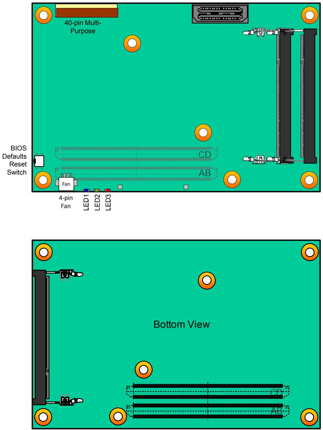
![The image displays two diagrams of a green circuit board, arranged vertically.\n\n**Top Diagram:**\nThis section shows the top side of the board.\n*   **Top Left:** A brown rectangular connector labeled '**40-pin Multi-Purpose**'.\n*   **Top Right:** A grey connector (resembling a legacy port).\n*   **Right Edge:** Two long, vertical black expansion slots.\n*   **Bottom Left:** A small switch labeled '**BIOS Defaults Reset Switch**'. Below it is a white connector labeled '**Fan**' with text underneath reading '**4-pin Fan**'. Next to it are three small colored squares labeled '**LED1**', '**LED2**', and '**LED3**'.\n*   **Center:** Two horizontal dashed rectangular outlines labeled '**CD**' and '**AB**'.\n*   **Mounting:** Orange circular holes with white centers are visible at the corners and specific intervals.\n\n**Bottom Diagram:**\nThis section is labeled '**Bottom View**' in the center.\n*   **Left Edge:** One long, vertical black expansion slot.\n*   **Bottom:** Two horizontal black slots enclosed in dashed outlines, labeled '**CD**' and '**AB**'.\n*   **Mounting:** Orange circular holes with white centers are visible at the corners and specific intervals.](.express-cf-cfe-50-1j095-1030-13/79e1c0cdd2f92998df4b45bb0fb72819dd225b7a5759ffec73d69e4ba7d07ae7.jpg)
Note: 3rd SO-DIMM socket on bottom side is supported by build option.

Figure 3: Express-CF/CFE Connector, Switch and LED Locations

# Express-CF/CFE and the DB40 Debug Module

For illustration purposes only
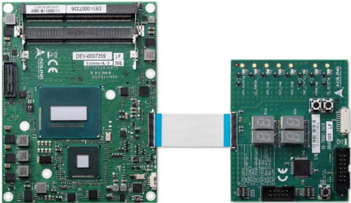
![DEV-0007359\nDFE-0007359\nDEV-0007359\nLF\nExpress-HL-5 200E\n51-772124-0A10\nCF-R-S 344-V\n1250E171928\nADLINK\nCE\nADLINK\nSYT-2007-0110\nDC-PLTRN\nSDE-524V\nSUS-24M\nSDE-559V\nSNC-S16U\nPNDINJW\nCELESETM\n51-75097-0A10\nDB40 CODE LF](.express-cf-cfe-50-1j095-1030-13/855bb2d4f89bd0681b59e2ba87612f9e289d5ae9e532db4c5a257bb3c3612e01.jpg)

Figure 4: Express-CF/CFE and the DB40 Debug Module

# 4.2 40-pin Debug Connector

FPC Connector Type: FCI 59GF Flex 10042867

Pin Orientation
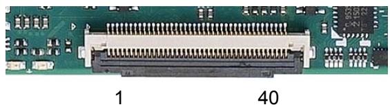
![Close-up of a green printed circuit board with a black connector and gold contacts, labeled with numbers 1 and 40 (no readable text beyond labels)](.express-cf-cfe-50-1j095-1030-13/c4144d2bbbe993bd7b60683e51522156bc8f648c78595d449866fe3b7d8e0fc7.jpg)

40-pin Debug Connector Pin Definition on the COM Express Module

<table><tr><td>Pin</td><td>Interface</td><td>Signal</td><td>Remark</td></tr><tr><td>40</td><td rowspan="7">SPI Program interface</td><td>VCC_SPI_IN</td><td>SPI Power Input from flash tool to module. HW need add MOS FET to switch SPI power for SPI ROM</td></tr><tr><td>39</td><td>GND</td><td></td></tr><tr><td>38</td><td>SPI_BIOS_CS 0#</td><td></td></tr><tr><td>37</td><td>SPI_BIOS_CS 1#</td><td></td></tr><tr><td>36</td><td>SPI_BIOS_MI SO</td><td></td></tr><tr><td>35</td><td>SPI_BIOS_M OSI</td><td></td></tr><tr><td>34</td><td>SPI_BIOS_CLK</td><td></td></tr><tr><td>33</td><td rowspan="10">LPC Bus</td><td>3V3_LPC</td><td>System power 3.3V provide from COM module</td></tr><tr><td>32</td><td>GND</td><td></td></tr><tr><td>31</td><td>BIOS_DIS0</td><td></td></tr><tr><td>30</td><td>RST#</td><td></td></tr><tr><td>29</td><td>CLK33_LPC</td><td></td></tr><tr><td>28</td><td>LPC_FRAME #</td><td></td></tr><tr><td>27</td><td>LPC_AD3</td><td></td></tr><tr><td>26</td><td>LPC_AD2</td><td></td></tr><tr><td>25</td><td>LPC_AD1</td><td>always power 3.3V provide from COM module</td></tr><tr><td>24</td><td>LPC_AD0</td><td></td></tr><tr><td>23</td><td rowspan="3">BMC Program interface</td><td>3.3V_BMC</td><td>always power 3.3V provide from COM module</td></tr><tr><td>22</td><td>3.3V_BMC</td><td>always power 3.3V provide from COM module</td></tr><tr><td>21</td><td>GND</td><td></td></tr></table>

<table><tr><td>Pin</td><td>Interface</td><td>Signal</td><td>Remark</td></tr><tr><td>20</td><td rowspan="8">BMC Program interface (cont&#x27;d)</td><td>TXD6</td><td></td></tr><tr><td>19</td><td>RXD6</td><td></td></tr><tr><td>18</td><td>FUMD0</td><td></td></tr><tr><td>17</td><td>RESET_IN#</td><td></td></tr><tr><td>16</td><td>DATA</td><td></td></tr><tr><td>15</td><td>CLK</td><td></td></tr><tr><td>14</td><td>OCD0A</td><td>Include a jumper to connect OCD0A via 1K0 pull-up to 3.3V_BMC</td></tr><tr><td>13</td><td>OCD0B</td><td>Include a jumper to connect OCD0A via 1K0 pull-up to 3.3V_BMC</td></tr><tr><td>12</td><td rowspan="7">Test points</td><td>PWRBTN#</td><td></td></tr><tr><td>11</td><td>SYS_RESET#</td><td></td></tr><tr><td>10</td><td>CB_RESET#</td><td></td></tr><tr><td>9</td><td>CB_PWROK</td><td></td></tr><tr><td>8</td><td>SUS_S3#</td><td></td></tr><tr><td>7</td><td>SUS_S4#</td><td></td></tr><tr><td>6</td><td>SUS_S5#</td><td></td></tr><tr><td>5</td><td rowspan="4">BMC Debug signals</td><td>POSTWDT_DIS #</td><td>Connect to Jumper for Debug</td></tr><tr><td>4</td><td>SEL_BIOS</td><td>Connect to Jumper for Debug</td></tr><tr><td>3</td><td>BIOS_MODE</td><td>Connect to Jumper for Debug</td></tr><tr><td>2</td><td>BMC_STATUS</td><td></td></tr><tr><td>1</td><td>Reserved</td><td></td><td></td></tr></table>

Table 2: 40-pin Debug Connector Pin Definition

Note: The pin definition on the debug module is the inverse of that on the COM Express module.

# 4.3 Status LEDs

To facilitate easier maintenance, status LED's are mounted on the board.

![Close-up of a green printed circuit board with various electronic components and connectors (no readable text or symbols)](.express-cf-cfe-50-1j095-1030-13/336ec5d13bdab5cebfd8b04c980985f56b4feae10947f67639bb27a11f0ea5f4.jpg)

LED1 LED2 LED3

LED Descriptions

<table><tr><td>Name</td><td>Color</td><td>Connection</td><td>Function</td></tr><tr><td>LED1</td><td>Blue</td><td>BMC output</td><td>Power Sequence Status Code (BMC)Power Changes, RESET(see 5.1.4 Exception Codes below)</td></tr><tr><td>LED2</td><td>Green</td><td>Power Source 3Vcc</td><td>S0 LED ONS3/S4/S5 LED OFFECO mode LED OFF</td></tr><tr><td>LED3</td><td>Red</td><td>BMC outputand same signal as WDT (B27) on BtB connector</td><td>Module power up WD LED = LED OFFWatchdog counting WD LED = Keep Last StateWatchdog timed out WD LED = LED ONWatchdog RESET WD LED = LED ONRebooted after WD RESET WD LED = LED ONRebooted after PWRBTN WD LED = LED OFFRebooted after RESET BTN WD LED = LED OFFNote: only a RESET not initiated by the BMC can clear the WD LED (user action)</td></tr></table>

Table 3: Express-CF/CFE LED Descriptions

# 4.4 Fan Connector

Connector Type: JVE 24W1125A-04M00

Pin Orientation
![Close-up of a green printed circuit board with various electronic components and connectors (no readable text or symbols)](.express-cf-cfe-50-1j095-1030-13/ba68a081d90c7b6208a279d52480e3d9966e50d33a7a8a3a7b797e5fee02ffd6.jpg)

1 2 3 4
Pin Assignment

<table><tr><td>Name</td><td>Description</td></tr><tr><td>1</td><td>FAN_PWMOUT</td></tr><tr><td>2</td><td>FAN_TACHIN</td></tr><tr><td>3</td><td>Ground</td></tr><tr><td>4</td><td>5V</td></tr></table>

Table 4: Fan Connector Pin Definition

# 4.5 BIOS Setup Defaults Reset Button

![Close-up of a green printed circuit board with electronic components and a circular component (no visible text or symbols)](.express-cf-cfe-50-1j095-1030-13/ebd4374f359eef7f89951e8e6eae4e372d588a80dc245dca132535afe9a28627.jpg)

To perform a hardware reset of BIOS default settings, perform the following steps:

1. Shut down the system.
2. Press the BIOS Setup Defaults RESET Button continuously and boot up the system. You can release the button when the BIOS prompt screen appears
3. The BIOS prompt screen will display a confirmation that BIOS defaults have been reset and request that you reboot the system.

![American\nMegatrends\nVersion 2.15.1236. Copyright (C) 2012 American Megatrends, Inc.\nExpress-HL REV:1.04\nPress (CTRL + P) to Enter MEBX setup menu\nPress (DEL) or (ESC) to enter setup.\nDefault settings had been loaded due to BIOS_DEFAULT jumper is set!\nPlease turn off system power and remove BIOS_DEFAULT jumper!](.express-cf-cfe-50-1j095-1030-13/a8264708b9673ef4342f03a4995e3514a352477ec174b23c2e7c59cd67d20e11.jpg)

# 4.6 Switch Settings

# Switch Locations

![BIOS Select and Mode Configuration Switch\nPCI Express Configuration Switch](.express-cf-cfe-50-1j095-1030-13/9888f380c2093f67714f78c9cbdc9bd144be1cdf8fdb3a93691977a05319666b.jpg)

Figure 5: Express-CF/CFE Switch Locations

# 4.6.1 PCI Express Configuration Switch.

PCI Express Configuration Switch (also referred to as the PEG config. switch) allows you to configure the PCI Express x16 lanes from the CPU as 1 PCIe x16, 2 PCIe x8, or 1 PCIe x8 + 2 PCIe x4.

<table><tr><td>Mode</td><td>Pin 1</td><td>Pin 2</td></tr><tr><td>1x PCIe x16 (default)</td><td>Off</td><td>Off</td></tr><tr><td>2x PCIe x8</td><td>On</td><td>Off</td></tr><tr><td>1x PCIe x8 + 2x PCIe x4</td><td>On</td><td>On</td></tr><tr><td>Reserved</td><td>Off</td><td>On</td></tr></table>

Table 5: PCI Express Configuration Switch Settings

# 4.6.2 BIOS Select and Mode Configuration Switch

The module has two BIOS chips and BIOS operation can be configured to "PICMG" and dual-BIOS "Failsafe" modes using BIOS Select and Mode Configuration Switch, Pin 2.

Setting the module to PICMG mode will configure the BIOS chips on the module as SPI0 and SPI1. In PICMG mode, a BIOS chip cannot be placed in the SPI0 slot on the carrier.

In dual-BIOS Failsafe mode, both BIOS chips on the module are configured as SPI1. Only one of the two is connected to the SPI bus at any given time. In case of failure of the primary SPI1 BIOS, the system will reboot and switch to the secondary SPI1 BIOS on the module. In Failsafe mode, the SPI0 BIOS socket on the carrier can be populated.

In either mode, BIOS Select and Mode Configuration Switch Pin 1 is used to select whether to boot from SPI0 or SPI1.

<table><tr><td>Mode</td><td>Pin 1</td><td>Pin 2</td></tr><tr><td>Boot from SPI0 (default)</td><td>On</td><td>—</td></tr><tr><td>Boot from SPI1</td><td>Off</td><td>—</td></tr><tr><td>Set BIOS to PICMG mode</td><td>—</td><td>On</td></tr><tr><td>Set BIOS to Failsafe BIOS mode (default)</td><td>—</td><td>Off</td></tr></table>

Table 6: BIOS Select and Mode Configuration Switch Settings

# 4.7 PCIe x16-to-two-x8 Adapter Card

The Express-CF/CFE can be used with the PCIe x16-to-two-x8 Adapter Card on the Express-BASE6 Reference Carrier to support bifurbication of the CPU's PEG interface (PCIe x16). The card reroutes the PCIe x16 to two x8 and allows testing of two independent PCIe add-on cards with x8/x4/x2/x1 width. To use the card, please refer to 4.6.1 PCI Express Configuration Switch. on page 39 and set the switch mode to "2x PCIe x8".

![Electronic component with green circuit board and gold contacts, no visible text or symbols on the main body](.express-cf-cfe-50-1j095-1030-13/bed16720f7962cca6171dfc9b4ef903c3e9dd97059bd70d7c77944d80aa6cd1e.jpg)

PClex16-to-two-x8 Adapter Card
(Model: P16TO28, Part No.: 91-79301-0010)

This page intentionally left blank.

# 5 Smart Embedded Management Agent (SEMA)

The onboard microcontroller (BMC) implements power sequencing and Smart Embedded Management Agent (SEMA) functionality. The microcontroller communicates via the System Management Bus with the CPU/chipset. The following functions are implemented:

• Total operating hours counter. Counts the number of hours the module has been run in minutes.
- On-time minutes counter. Counts the seconds since last system start.
- Temperature monitoring of CPU and board temperature. Minimum and maximum temperature values of CPU and board are stored in flash.
• Power cycles counter
- Boot counter. Counts the number of boot attempts.
- Watchdog Timer. Set/Reset/Disable Watchdog Timer. Features auto-reload at power-up.
• System Restart Cause. Power loss/BIOS Fail/Watchdog/Internal Reset/External Reset
- Fail-safe BIOS support. In case of a boot failure, hardware signals tells external logic to boot from fail-safe BIOS.
• Flash area. 1kB Flash area for customer data
• 2K Bytes Protected Flash area. Keys, IDs, etc. can be stored in a write- and clear-protectable region.
• Board Identify. Vendor/Board/Serial number/Production Date
• Main-current & voltage. Monitors drawn current and main voltages

For a detailed description of SEMA features and functionality, please refer to SEMA Technical Manual and SEMA Software Manual, downloadable at: http://www.adlinktech.com/sema/.

# 5.1 Board Specific SEMA Functions

# 5.1.1 Voltages

The BMC of the Express-CF/CFE implements a voltage monitor and samples several onboard voltages. The voltages can be read by calling the SEMA function “Get Voltages”. The function returns a 16-bit value divided into high-byte (MSB) and low-byte (LSB).

<table><tr><td>ADC Channel</td><td>Voltage Name</td><td>Voltage Formula [V]</td></tr><tr><td>0</td><td>VCORE</td><td>(MSB&lt;&lt;8 + LSB) x 1 x 3.3 / 1024</td></tr><tr><td>1</td><td>VCC_GT</td><td>(MSB&lt;&lt;8 + LSB) x 1 x 3.3 / 1024</td></tr><tr><td>2</td><td>1V05_A</td><td>(MSB&lt;&lt;8 + LSB) x 1 x 3.3 / 1024</td></tr><tr><td>3</td><td>VDDQ</td><td>(MSB&lt;&lt;8 + LSB) x 1 x 3.3 / 1024</td></tr><tr><td>4</td><td>VRTC</td><td>(MSB&lt;&lt;8 + LSB) x 1.01 x 3.3 / 1024</td></tr><tr><td>5</td><td>V3P3S</td><td>(MSB&lt;&lt;8 + LSB) x 1.1 x 3.3 / 1024</td></tr><tr><td>6</td><td>V3P3A</td><td>(MSB&lt;&lt;8 + LSB) x 1.100 x 3.3 / 1024</td></tr><tr><td>7</td><td>V5S</td><td>(MSB&lt;&lt;8 + LSB) x 1.826 x 3.3 / 1024</td></tr><tr><td>8</td><td>VCCST</td><td>(MSB&lt;&lt;8 + LSB) x 1 x 3.3 / 1024</td></tr><tr><td>9</td><td>VCCIO</td><td>(MSB&lt;&lt;8 + LSB) x 1 x 3.3 / 1024</td></tr><tr><td>10</td><td>VCCSTG</td><td>(MSB&lt;&lt;8 + LSB) x 1 x 3.3 / 1024</td></tr><tr><td>11</td><td>VCCSA</td><td>(MSB&lt;&lt;8 + LSB) x 1 x 3.3 / 1024</td></tr><tr><td>12</td><td>1V8_A</td><td>(MSB&lt;&lt;8 + LSB) x 1 x 3.3 / 1024</td></tr><tr><td>13</td><td>V5SBY</td><td>(MSB&lt;&lt;8 + LSB) x 1.826 x 3.3 / 1024</td></tr><tr><td>14</td><td>V12</td><td>(MSB&lt;&lt;8 + LSB) x 6 x 3.3 / 1024</td></tr><tr><td>15</td><td>(MAIN CURRENT)</td><td>Use Main Current Function</td></tr></table>

Table 7: SEMA Onboard Voltage Monitor

# 5.1.2 Main Current

The BMC of the Express-CF/CFE implements a current monitor. The current can be read by calling the SEMA function “Get Main Current”. The function returns four 16-bit values divided in high-byte (MSB) and low-byte (LSB). These 4 values represent the last 4 currents drawn by the board. The values are sampled every 250ms. The order of the 4 values is NOT in chronological order. Access by the BMC may increase the drawn current of the whole system. In this case, there are still 3 samples not influenced by the read access.

$$
\text { Main   Current } = (\text { MSB\_n } &lt;   &lt;   8 + \text { LSB\_n }) \times 8. 0 6 \mathrm{mA}
$$

# 5.1.3 BMC Status

This register shows the status of BMC controlled signals on the Express-CF/CFE.

&lt;table&gt;<tr><td>Status Bit</td><td>Signal</td></tr><tr><td>0</td><td>WDT_OUT</td></tr><tr><td>1</td><td>LVDS_VDDEN</td></tr><tr><td>2</td><td>LVDS_BKLTEN</td></tr><tr><td>3</td><td>BIOS_MODE</td></tr><tr><td>4</td><td>POSTWDT_DISn</td></tr><tr><td>5</td><td>SEL_BIOS</td></tr><tr><td>6</td><td>BIOS_DIS0n</td></tr><tr><td>7</td><td>BIOS_DIS1n</td></tr></table>

Table 8: SEMA BMC Status

# 5.1.4 Exception Codes

In case of an error, the BMC drives a blinking code on the blue Status LED (LED1). The same error code is also reported by the BMC Flags register. The Exception Code is not stored in the Flash Storage and is cleared when the power is removed. Therefore, a “Clear Exception Code” command is not needed or supported.

<table><tr><td>Exception Code</td><td>Error Message</td></tr><tr><td>0</td><td>NOERROR</td></tr><tr><td>2</td><td>NO_SUSCLK</td></tr><tr><td>3</td><td>NO_SLP_S5</td></tr><tr><td>4</td><td>NO_SLP_S4</td></tr><tr><td>5</td><td>NO_SLP_S3</td></tr><tr><td>6</td><td>BIOS_FAIL</td></tr><tr><td>7</td><td>RESET_FAIL</td></tr><tr><td>8</td><td>RESETIN_FAIL</td></tr><tr><td>9</td><td>NO_CB_PWROK</td></tr><tr><td>10</td><td>CRITICAL_TEMP</td></tr><tr><td>11</td><td>POWER_FAIL</td></tr><tr><td>12</td><td>VOLTAGE_FAIL</td></tr><tr><td>14</td><td>NO_VDDQ_PG</td></tr><tr><td>15</td><td>NO_V1P05S_PG</td></tr><tr><td>16</td><td>NO_VCORE_PG</td></tr><tr><td>17</td><td>NO_SYS_GD</td></tr><tr><td>18</td><td>NO_V5SBY</td></tr><tr><td>19</td><td>NO_V3P3A</td></tr></table>

<table><tr><td>Exception Code</td><td>Error Message</td></tr><tr><td>20</td><td>NO_V5_DUAL</td></tr><tr><td>21</td><td>NO_PWRSRC_GD</td></tr><tr><td>22</td><td>NO_P_5V_3V3_S0_PG</td></tr></table>

Table 9: SEMA Exception Codes

# 5.1.5 BMC Flags

The BMC Flags register returns the last detected Exception Code since power-up and shows the BIOS in use and the power mode.

<table><tr><td>Bit</td><td>Description</td></tr><tr><td>[0 ~ 4]</td><td>Exception Code</td></tr><tr><td>[6]</td><td>0 = AT mode1 = ATX mode</td></tr><tr><td>[7]</td><td>0 = Standard BIOS1 = Fail-safe BIOS.</td></tr></table>

Table 10: SEMA BMC Flags

# 6 System Resources

# 6.1 System Memory Map

<table><tr><td>Address Range (hex)</td><td>Description</td></tr><tr><td>FF000000-FFFFFFFF</td><td>Motherboard resources</td></tr><tr><td>FEE00000-FEEFFFFF</td><td>Motherboard resources</td></tr><tr><td>FED45000-FED93FFF</td><td>Motherboard resources</td></tr><tr><td>FED40000-FED44FFF</td><td>Trusted Platform Module 2.0</td></tr><tr><td>FED10000-FED3FFFF</td><td>Motherboard resources</td></tr><tr><td>FED00000-FED003FF</td><td>High precision event timer</td></tr><tr><td>FC800000-FE7FFFFFF</td><td>PCI Express Root Complex</td></tr><tr><td>E0000000-EFFFFFFFF</td><td>Motherboard resources</td></tr><tr><td>8F800000-DFFFFFFFF</td><td>PCI Express Root Complex</td></tr><tr><td>000A0000-000BFFFF</td><td>PCI Express Root Complex</td></tr><tr><td>00000 – FFFFFFF</td><td>DOS Compatibility Memory</td></tr></table>

# 6.2 I/O Map

<table><tr><td>Hex Range</td><td>Device</td></tr><tr><td>20h – 21h</td><td>Interrupt Controller</td></tr><tr><td>24h – 25h</td><td>Interrupt Controller</td></tr><tr><td>28h – 29h</td><td>Interrupt Controller</td></tr><tr><td>2Ch – 2Dh</td><td>Interrupt Controller</td></tr><tr><td>2E-02F</td><td>Motherboard resources</td></tr><tr><td>30h – 31h</td><td>Interrupt Controller</td></tr><tr><td>34h – 35h</td><td>Interrupt Controller</td></tr><tr><td>38h – 39h</td><td>Interrupt Controller</td></tr><tr><td>3Ch – 3Dh</td><td>Interrupt Controller</td></tr><tr><td>40h – 43h</td><td>System timer</td></tr><tr><td>4Eh – 4Fh</td><td>Motherboard resources</td></tr><tr><td>50h – 53h</td><td>System timer</td></tr><tr><td>60h</td><td>Standard PS/2 Keyboard</td></tr><tr><td>61h</td><td>Motherboard resources</td></tr><tr><td>62h</td><td>Microsoft ACPI-Compliant Embedded Controller</td></tr><tr><td>63h</td><td>Motherboard resource</td></tr><tr><td>64h</td><td>Standard PS/2 Keyboard</td></tr><tr><td>65h</td><td>Motherboard resources</td></tr><tr><td>66h</td><td>Microsoft ACPI-Compliant Embedded Controller</td></tr><tr><td>67h</td><td>Motherboard resources</td></tr><tr><td>70h</td><td>RTC Controller</td></tr><tr><td>71h</td><td>RTC Controller</td></tr><tr><td>72h</td><td>RTC Controller</td></tr><tr><td>73h</td><td>RTC Controller</td></tr><tr><td>74h</td><td>RTC Controller</td></tr><tr><td>75h</td><td>RTC Controller</td></tr><tr><td>76h – 77h</td><td>RTC Controller</td></tr><tr><td>80h</td><td>Motherboard resources</td></tr><tr><td>92h</td><td>Motherboard resources</td></tr><tr><td>A0h – A1h</td><td>Interrupt Controller</td></tr><tr><td>B2h – B3h</td><td>Motherboard resources</td></tr><tr><td>B4h – B5h</td><td>Interrupt Controller</td></tr><tr><td>B8h – B9h</td><td>Interrupt Controller</td></tr><tr><td>BCh – BDh</td><td>Interrupt Controller</td></tr><tr><td>240h – 247h</td><td>Communications Port (COM3)</td></tr><tr><td>248h – 24Fh</td><td>Communications Port (COM4)</td></tr><tr><td>2F8h – 2FFh</td><td>Communications Port (COM2)</td></tr><tr><td>3F8h – 3FFh</td><td>Communications Port (COM1)</td></tr><tr><td>4D0h – 4D1h</td><td>Interrupt Controller</td></tr><tr><td>680h – 69Fh</td><td>Motherboard resources</td></tr><tr><td>6A0h</td><td>Motherboard resources</td></tr><tr><td>CF9h</td><td>Reset Generator</td></tr></table>

# 6.3 Interrupt Request (IRQ) Lines

Note (1): These IRQs can be used for PCI devices when onboard device is disabled.
PIC Mode

<table><tr><td>IRQ#</td><td>Typical Interrupt Resource</td><td>Connected to Pin</td><td>Available</td></tr><tr><td>0</td><td>Counter 0</td><td>N/A</td><td>No</td></tr><tr><td>1</td><td>Keyboard controller</td><td>IRQ1 via SERIRQ</td><td>No</td></tr><tr><td>2</td><td>Cascade interrupt from slave PIC</td><td>N/A</td><td>No</td></tr><tr><td>3</td><td>Serial Port 4 (COM4)</td><td>IRQ3 via SERIRQ / PIRQ</td><td>Note (1)</td></tr><tr><td>4</td><td>Serial Port 3 (COM3)</td><td>IRQ4 via SERIRQ / PIRQ</td><td>Note (1)</td></tr><tr><td>5</td><td>Serial Port 1 (COM1)</td><td>IRQ5 via SERIRQ / PIRQ</td><td>Note (1)</td></tr><tr><td>6</td><td>Generic</td><td>IRQ6 via SERIRQ / PIRQ</td><td>No</td></tr><tr><td>7</td><td>Serial Port 2 (COM2)</td><td>IRQ7 via SERIRQ / PIRQ</td><td>Note (1)</td></tr><tr><td>8</td><td>Real-time clock</td><td>N/A</td><td>No</td></tr><tr><td>9</td><td>Generic</td><td>N/A</td><td>Note (1)</td></tr><tr><td>10</td><td>Generic</td><td>IRQ10 via SERIRQ / PIRQ</td><td>Note (1)</td></tr><tr><td>11</td><td>Generic</td><td>IRQ11 via SERIRQ / PIRQ</td><td>Note (1)</td></tr><tr><td>12</td><td>PS/2 Mouse</td><td>IRQ12 via SERIRQ / PIRQ</td><td>Note (1)</td></tr><tr><td>13</td><td>GSPI, UART, I2C, SDIO</td><td>N/A</td><td>Note (1)</td></tr><tr><td>14</td><td>Gpio</td><td>PIRQ</td><td>Note (1)</td></tr><tr><td>15</td><td>Gpio</td><td>PIRQ</td><td>Note (1)</td></tr></table>

APIC Mode

<table><tr><td>IRQ#</td><td>Typical Interrupt Resource</td><td>Connected to Pin</td><td>Available</td></tr><tr><td>0</td><td>Counter 0</td><td>N/A</td><td>No</td></tr><tr><td>1</td><td>Keyboard controller</td><td>IRQ1 via SERIRQ</td><td>No</td></tr><tr><td>2</td><td>Cascade interrupt from slave PIC</td><td>N/A</td><td>No</td></tr><tr><td>3</td><td>Serial Port 4 (COM4)</td><td>IRQ3 via SERIRQ</td><td>Note (1)</td></tr><tr><td>4</td><td>Serial Port 3 (COM3)</td><td>IRQ4 via SERIRQ</td><td>Note (1)</td></tr><tr><td>5</td><td>Serial Port 1 (COM1)</td><td>IRQ5 via SERIRQ</td><td>Note (1)</td></tr><tr><td>6</td><td>N/A</td><td>N/A</td><td>Note (1)</td></tr><tr><td>7</td><td>Serial Port 2 (COM1)</td><td>IRQ7 via SERIRQ</td><td>Note (1)</td></tr><tr><td>8</td><td>Real-time clock</td><td>N/A</td><td>No</td></tr><tr><td>9</td><td>N/A</td><td>N/A</td><td>Note (1)</td></tr><tr><td>10</td><td>N/A</td><td>N/A</td><td>Note (1)</td></tr><tr><td>11</td><td>N/A</td><td>N/A</td><td>Note (1)</td></tr><tr><td>12</td><td>PS/2 Mouse</td><td>IRQ12 via SERIRQ</td><td>Note (1)</td></tr><tr><td>13</td><td>Math Processor</td><td>N/A</td><td>Note (1)</td></tr><tr><td>14</td><td>SATA Primary</td><td>IRQ14 via SERIRQ</td><td>Note (1)</td></tr><tr><td>15</td><td>SATA Secondary</td><td>IRQ15 via SERIRQ</td><td>Note (1)</td></tr><tr><td>16</td><td>N/A</td><td>P.E.G Root Port,Intel HDA, PCIE Port 0/1/2/3/4/5/6, I.G.D., XHCI Controller</td><td>Note (1)</td></tr><tr><td>17</td><td>N/A</td><td>PCIE Port 0/1/2/3/4/5/6, P.E.G Root Port,</td><td>Note (1)</td></tr><tr><td>18</td><td>N/A</td><td>PCIE Port 0/1/2/3/4/5/6, P.E.G Root Port, SMBus Controller</td><td>Note (1)</td></tr><tr><td>19</td><td>N/A</td><td>PCIE Port 0/1/2/3/4/5/6, P.E.G Root Port,</td><td>Note (1)</td></tr></table>

Note (1): These IRQs can be used for PCI devices when onboard device is disabled.

6.4 PCI Configuration Space Map

<table><tr><td>Bus Number</td><td>Device Number</td><td>Function Number</td><td>Routing</td><td>Description</td></tr><tr><td>00h</td><td>00h</td><td>00h</td><td>N/A</td><td>Intel host Bridge</td></tr><tr><td>00h</td><td>02h</td><td>00h</td><td>Internal</td><td>Intel I.G.D.</td></tr><tr><td>00h</td><td>08h</td><td>00h</td><td>Internal</td><td>Gaussian Mixture Model</td></tr><tr><td>00h</td><td>12h</td><td>00h</td><td>Internal</td><td>Thermal Subsystem</td></tr><tr><td>00h</td><td>14h</td><td>00h</td><td>Internal</td><td>xHCI Controller</td></tr><tr><td>00h</td><td>14h</td><td>02h</td><td>Internal</td><td>Intel RAM</td></tr><tr><td>00h</td><td>14h</td><td>05h</td><td>Internal</td><td>Intel Corporation System Device</td></tr><tr><td>00h</td><td>16h</td><td>00h</td><td>Internal</td><td>Intel Management Engine Interface</td></tr><tr><td>00h</td><td>16h</td><td>03h</td><td>Internal</td><td>Intel Active Management Technology - SOL</td></tr><tr><td>00h</td><td>17h</td><td>00h</td><td>Internal</td><td>Intel AHCI controller</td></tr><tr><td>00h</td><td>1Bh</td><td>00h</td><td>Internal</td><td>Intel PCI Express Root port 5</td></tr><tr><td>00h</td><td>1Bh</td><td>01h</td><td>Internal</td><td>Intel PCI Express Root port 6</td></tr><tr><td>00h</td><td>1Bh</td><td>02h</td><td>Internal</td><td>Intel PCI Express Root port 7</td></tr><tr><td>00h</td><td>1Bh</td><td>03h</td><td>Internal</td><td>Intel PCI Express Root port 8</td></tr><tr><td>00h</td><td>1Dh</td><td>00h</td><td>Internal</td><td>Intel PCI Express Root port 1</td></tr><tr><td>00h</td><td>1Dh</td><td>01h</td><td>Internal</td><td>Intel PCI Express Root port 2</td></tr><tr><td>00h</td><td>1Dh</td><td>02h</td><td>Internal</td><td>Intel PCI Express Root port 3</td></tr><tr><td>00h</td><td>1Dh</td><td>03h</td><td>Internal</td><td>Intel PCI Express Root port 4</td></tr><tr><td>00h</td><td>1Fh</td><td>00h</td><td>Internal</td><td>Intel LPC Interface Bridge</td></tr><tr><td>00h</td><td>1Fh</td><td>03h</td><td>Internal</td><td>HDA Controller</td></tr><tr><td>00h</td><td>1Fh</td><td>04h</td><td>Internal</td><td>SMBus Controller</td></tr><tr><td>00h</td><td>1Fh</td><td>05h</td><td>Internal</td><td>SPI</td></tr><tr><td>00h</td><td>1Fh</td><td>06h</td><td>Internal</td><td>GbE Controller</td></tr></table>

# 6.5 PCI Interrupt Routing Map

<table><tr><td>INT Line</td><td>P.E.G. Root Port</td><td>IGFX</td><td>LPC Bridge</td><td>HD Audio Controller</td><td>SMBus</td><td>GbE Controller</td></tr><tr><td>Int0</td><td>INTA:16</td><td>INTA:16</td><td>INTA:16</td><td>INTA:16</td><td>INTA:16</td><td>INTA:16</td></tr><tr><td>Int1</td><td>INTB:17</td><td></td><td>INTD:17</td><td></td><td></td><td></td></tr><tr><td>Int2</td><td>INTC:18</td><td></td><td>INTC:18</td><td></td><td></td><td></td></tr><tr><td>Int3</td><td>INTD:19</td><td></td><td>INTB:19</td><td></td><td></td><td></td></tr></table>

<table><tr><td>INT Line</td><td>SATA Controller</td><td>ME Controller</td><td>XHCI Controller</td><td>Thermal Subsystem</td></tr><tr><td>Int0</td><td>INTA:16</td><td>INTA:16</td><td>INTA:16</td><td>INTA:16</td></tr><tr><td>Int1</td><td></td><td>INTB:17</td><td>INTB:17</td><td>INTB:17</td></tr><tr><td>Int2</td><td></td><td>INTC:18</td><td>INTC:18</td><td>INTC:18</td></tr><tr><td>Int3</td><td></td><td>INTD:19</td><td>INTD:19</td><td>INTD:19</td></tr></table>

<table><tr><td>INT Line</td><td>PCIE Port1</td><td>PCIE Port 2</td><td>PCIE Port 3</td><td>PCIE Port 4</td><td>PCIE Port 5</td><td>PCIE Port 6</td><td>PCIE Port 7</td><td>PCIE Port 8</td></tr><tr><td>Int0</td><td>INTA:16</td><td>INTB:17</td><td>INTC:18</td><td>INTD:19</td><td>INTA:16</td><td>INTB:17</td><td>INTC:18</td><td>INTD:19</td></tr><tr><td>Int1</td><td>INTB:17</td><td>INTC:18</td><td>INTD:19</td><td>INTA:16</td><td>INTB:17</td><td>INTC:18</td><td>INTD:19</td><td>INTA:16</td></tr><tr><td>Int2</td><td>INTC:18</td><td>INTD:19</td><td>INTA:16</td><td>INTB:17</td><td>INTC:18</td><td>INTD:19</td><td>INTA:16</td><td>INTB:17</td></tr><tr><td>Int3</td><td>INTD:19</td><td>INTA:16</td><td>INTB:17</td><td>INTC:18</td><td>INTD:19</td><td>INTA:16</td><td>INTB:17</td><td>INTC:18</td></tr></table>

# 6.6 SMBus Address Table

<table><tr><td>Device</td><td>Address</td></tr><tr><td>DDR4 Channel A(SO-DIMM1)</td><td>A0h</td></tr><tr><td>DDR4 Channel B(SO-DIMM2)</td><td>A4h</td></tr><tr><td>DDR4 Channel B(SO-DIMM3)</td><td>A6h</td></tr><tr><td>Thermal Sensor</td><td>92h</td></tr><tr><td>BMC</td><td>50h</td></tr><tr><td>Extend GPIO (PCA9535)</td><td>40h</td></tr><tr><td>NXP (eDP to LVDS transmitter)</td><td>C0h</td></tr></table>

This page intentionally left blank.

# 7 BIOS Setup

# 7.1 Menu Structure

This section presents the six primary menus of the BIOS Setup Utility. Use the following table as a quick reference for the contents of the BIOS Setup Utility. The subsections in this section describe the Submenus and setting options for each menu item. The default setting options are presented in bold, and the function of each setting is described in the right hand column of the respective table.

<table><tr><td>Main</td><td>Advanced</td><td>Chipset</td><td>Security</td><td>Boot</td><td>Save &amp; Exit</td></tr><tr><td>BIOS Information System Information Board Information ▶System Date System Time</td><td>CPU Configuration ▶Graphics Configuration ▶Power Management ▶USB Configuration ▶Network Stack Configuration ▶System Management ▶Thermal Management ▶Watchdog Timer ▶Super IO Configuration ▶Serial Console Redirection ▶Miscellaneous ▶AMI Graphic Output Protocol Policy ▶</td><td>System Agent (SA) Configuration ▶PCH-IO Configuration ▶</td><td>Password Description Secure Boot Menu ▶</td><td>Boot Configuration</td><td>Save Options Boot Override</td></tr></table>

# Notes:

▶ indicates a Submenu
Gray text indicates info only

# 7.2 Main

The Main Menu provides read-only information about your system and also allows you to set the System Date and Time. Refer to the tables below the screen shot of this menu for details of the Submenus and settings.

# 7.2.1 BIOS Information

<table><tr><td>Feature</td><td>Options</td><td>Description</td></tr><tr><td>BIOS Vender</td><td>Info only</td><td>American Megatrends</td></tr><tr><td>BIOS Version</td><td>Info only</td><td>Display Core version</td></tr><tr><td>Build Date</td><td>Info only</td><td>Display Build Date</td></tr><tr><td>MRC Version</td><td>Info only</td><td>Display MRC information</td></tr><tr><td>GOP Version</td><td>Info only</td><td>Display GOP version.</td></tr><tr><td>ME FW Version</td><td>Info only</td><td>Display ME FW version.</td></tr><tr><td>BIOS Boot Source</td><td>Info only</td><td>SPI Boot Source</td></tr></table>

# 7.2.2 System Information

<table><tr><td>Board Information</td><td>Info only</td><td>Description</td></tr><tr><td>Project Name</td><td>Info only</td><td>Display Project Name.</td></tr><tr><td>CPU Board Version</td><td>Info only</td><td>Display CPU signature.</td></tr><tr><td>CPU Brand String</td><td>Info only</td><td>Display CPU brand name.</td></tr><tr><td>Stepping</td><td>Info only</td><td>Display CPU stepping.</td></tr><tr><td>GT Info</td><td>Info only</td><td>Display GT info of Intel Graphics.</td></tr><tr><td>CPU Frequency</td><td>Info only</td><td>Display CPU frequency</td></tr><tr><td>Total Memory</td><td>Info only</td><td>Display installed memory size.</td></tr><tr><td>Memory Frequency</td><td>Info only</td><td>Display memory frequency.</td></tr><tr><td>PCH SKU</td><td>Info only</td><td>Display PCH information.</td></tr><tr><td>Stepping</td><td>Info only</td><td>Display PCH stepping.</td></tr><tr><td>Board Information</td><td>Submenu</td><td></td></tr></table>

# 7.2.3 Board Information

<table><tr><td>Board Information</td><td>Info only</td><td>Description</td></tr><tr><td>Serial Number</td><td>Read only</td><td>Display SMC serial number</td></tr><tr><td>Manufacturing Date</td><td>Read only</td><td>Display SMC manufacturing date.</td></tr><tr><td>Last Repair Date</td><td>Read only</td><td>Display SMC last repair date.</td></tr><tr><td>MAC ID</td><td>Read only</td><td>Display SMC MAC ID.</td></tr><tr><td>Runtime Statistics</td><td colspan="2">Info only</td></tr><tr><td>Total Runtime</td><td>Read only</td><td>The returned value specifies the total time in minutes the system is running in S0 state.</td></tr><tr><td>Current Runtime</td><td>Read only</td><td>The returned value specifies the time in seconds the system is running in S0 state.This counter is cleared when the system is removed from the external power supply.</td></tr><tr><td>Power Cycles</td><td>Read only</td><td>The returned value specifies the number of times the external power supply has been shut down.</td></tr><tr><td>Boot Cycles</td><td>Read only</td><td>The Bootcounter is increased after a HW- or SW-Reset or after a successful power-up.</td></tr><tr><td>Boot Reason</td><td>Read only</td><td>The boot reason is the event which causes the reboot of the system.</td></tr></table>

# 7.2.4 System Date and Time

<table><tr><td>Feature</td><td>Options</td><td>Description</td></tr><tr><td>System Date</td><td>Weekday, MM/DD/YYYY</td><td>Requires the alpha-numeric entry of the day of the week, day of the month, calendar month, and all 4 digits of the year, indicating the century and year (Fri XX/XX/20XX)</td></tr><tr><td>System Time</td><td>HH/MM/SS</td><td>Presented as a 24-hour clock setting in hours, minutes, and seconds</td></tr></table>

# 7.3 Advanced

This menu contains the settings for most of the user interfaces in the system

7.3.1 CPU Configuration

<table><tr><td>Feature</td><td>Options</td><td>Description</td></tr><tr><td>Type</td><td>Info only</td><td>Display CPU information.</td></tr><tr><td>ID</td><td>Info only</td><td>Display CPU information.</td></tr><tr><td>Microcode Revision</td><td>Info only</td><td>Display CPU Microcode Revision.</td></tr><tr><td>Speed</td><td>Info only</td><td>Display CPU frequency.</td></tr><tr><td>L1 Data Cache</td><td>Info only</td><td>Display cache info.</td></tr><tr><td>L1 Instruction Cache</td><td>Info only</td><td>Display cache info.</td></tr><tr><td>L2 Cache</td><td>Info only</td><td>Display cache info.</td></tr><tr><td>L3 Cache</td><td>Info only</td><td>Display cache info.</td></tr><tr><td>L4 Cache</td><td>Info only</td><td>Display cache info.</td></tr><tr><td>VMX</td><td>Info only</td><td>Display Intel Virtualization Technology support or not.</td></tr><tr><td>SMX/TXT</td><td>Info only</td><td>Display Intel SMX Technology support or not.</td></tr><tr><td>Boot performance mode</td><td>Max Battery Max Non-Turbo Performance Turbo Performance</td><td>Select the performance state that the BIOS will set starting from reset vector.</td></tr><tr><td>Hyper-Threading</td><td>Disabled Enabled</td><td>Enabled for Windows XP and Linux (OS optimized for Hyper-Threading Technology) and Disabled for other OS (OS not optimized for Hyper-Threading Technology).</td></tr><tr><td>Intel(R) SpeedStep(tm)</td><td>Disabled Enabled</td><td>Allows more than two frequency ranges to be supported.</td></tr><tr><td>Intel(R) Speed Shift Technology</td><td>Disabled Enabled</td><td>Enable/Disable Intel(R) Speed Shift Technology support. Enabling will expose the CPPC v2 interface to allow for hardware controlled P-states</td></tr><tr><td>Turbo Mode</td><td>Disabled Enabled</td><td>Enable/Disable processor Turbo Mode (requires Intel Speed Step or Intel Speed Shift to be available and enabled).</td></tr><tr><td>Configurable TDP Boot Mode</td><td>Nominal Down Deactivate</td><td>Configurable TDP Mode as Nominal/Up/Down/Deactivate TDP selection. Deactivate option will set MSR to Nominal and MMIO to Zero.</td></tr><tr><td>Platform PL1 Enable</td><td>Disabled Enabled</td><td>Enabled for Windows XP and Linux (OS optimized for Hyper-Threading Technology) and Disabled for other OS (OS not optimized for Hyper-Threading Technology). When Disabled only one thread per enabled core is enabled.</td></tr><tr><td>Platform PL1 Power</td><td>0</td><td>Platform Power Limit 1 Power in Milli Watts. BIOS will round to the nearest 1/8W when programming. Any value can be programmed between Max and Min Power Limits (specified by PACKAGE_POWER_SKU_MSR). For 12.50W, enter 12500. This setting will act as the new PL1 value forthe Package RAPL algorithm.</td></tr><tr><td>Platform PL1 Time Window</td><td>0</td><td>Platform Power Limit 1 Time Window value in seconds. The value may vary from 0 to 128. 0 = default values. Indicates the time window over which Platform TDP value should be maintained.</td></tr><tr><td>C states</td><td>DisabledEnabled</td><td>Enable/Disable CPU Power Management. Allows CPU to go to C states when it's not 100% utilized.</td></tr><tr><td>Package C State Limit</td><td>C0/C1C2C3C6C7C7SC8C9C10CPU DefaultAuto</td><td>Maximum Package C State Limit Setting. Cpu Default: Leaves to Factory default value.Auto: Initializes to deepest available Package C State Limit.</td></tr><tr><td>Active Processor Cores</td><td>All12345678</td><td>Number of cores to enable in each processor package.</td></tr><tr><td>VT-d</td><td>DisabledEnabled</td><td>VT-d capability.</td></tr><tr><td>DTS SMM</td><td>DisabledEnabledCritical Temp Reporting (Out of spec)</td><td>Disabled: ACPI thermal management uses EC reported temperature values.</td></tr><tr><td>Intel Trusted Execution Technology</td><td>DisabledEnabled</td><td>Enables utilization of additional hardware capabilities provided by Intel (R) Trusted Execution Technology.</td></tr></table>

7.3.2 Graphics Configuration

<table><tr><td>Feature</td><td>Options</td><td>Description</td></tr><tr><td>LVDS</td><td colspan="2">Info only</td></tr><tr><td>Data format and Color Depth</td><td>VESA 24 bppJEIDA 24 bppJEIDA/VESA 18 bpp</td><td>Data format and Color Depth select</td></tr><tr><td>LVDS Output Mode</td><td>Dual LVDS busSingle LVDS bus</td><td>Single/Dual mode select.</td></tr><tr><td>DE Polarity</td><td>Active HighActive Low</td><td>DE Polarity select.</td></tr><tr><td>Hsync Polarity</td><td>Active HighActive Low</td><td>Hsync Polarity select.</td></tr><tr><td>LVDS Backlight Mode</td><td>BMC ModeGTT Mode</td><td>Select LVDS Backlight control function.</td></tr><tr><td>LVDS Backlight Brightness</td><td>FF</td><td>A change takes effect immediately.</td></tr><tr><td>Brightness Setting</td><td>255</td><td>Set GOP Brightness value</td></tr><tr><td>Integrated Display Configuration</td><td colspan="2">Info only</td></tr><tr><td>eDP/LVDS</td><td>DisableEnable</td><td>Enable/Disable eDP/LVDS</td></tr><tr><td>DDI port 1</td><td>No DeviceDisplay PortHDMIDisplayPort with HDMI/DVI Compatible</td><td>Set DDI port 1 function to DisplayPort or HDMI.</td></tr><tr><td>DDI port 2</td><td>No DeviceDisplay PortHDMIDisplayPort with HDMI/DVI Compatible</td><td>Set DDI port 2 to DisplayPort or HDMI.</td></tr><tr><td>DDI port 3</td><td>No DeviceDisplay PortHDMIDisplayPort with HDMI/DVI Compatible*</td><td>Set DDI port 3 function to DisplayPort or HDMI.*Note: Default is “HDMI” if the module supports the DP-to-VGA build option.</td></tr><tr><td>LFP Panel Type</td><td>Default640x480800x6001024x7681280x10241400x1050 LVDS11400x1050 LVDS21600x12001366x7681680x10501920x12001440x9001600x9001024x7681280x8001920x10802048x1536</td><td>Select LFP panel used by Internal Graphics Device by selecting the appropriate setup item.</td></tr><tr><td>DP To VGA Function*</td><td>DisabledEnabled</td><td>Enable/Disable DP To VGA Function*Note: This option is hidden unless the module supports the DP-to-VGA build option.</td></tr></table>

# 7.3.3 Power Management

<table><tr><td>Feature</td><td>Options</td><td>Description</td></tr><tr><td>Power Management</td><td colspan="2">Info only</td></tr><tr><td>Enable ACPI Auto Configuration</td><td>DisabledEnabled</td><td>Enables or Disables BIOS ACPI Auto Configuration.</td></tr><tr><td>Enable Hibernation</td><td>DisabledEnabled</td><td>Enables or Disables System ability to Hibernate (OS/S4 Sleep State). This option may not be effective with some operating systems.</td></tr><tr><td>ACPI Sleep State</td><td>Suspend DisabledS3 (Suspend to RAM)</td><td>Select the highest ACPI sleep state the system will enter when the SUSPEND button is pressed.</td></tr><tr><td>LID Function</td><td>DisabledEnabled</td><td>Enable/Disable LID Function</td></tr><tr><td>ECO Mode</td><td>DisabledEnabled</td><td>Reduces the power consumption of the system, but after a shut down, you have to wait at least 5 seconds before you can restart the system.</td></tr><tr><td>Power-Up Mode</td><td>Turn OnRemain OffLast State</td><td>Turn On:The machine starts automatically when the power supply is turned on.Remain off:To start the machine the power button has to pressed.Last State:The machine will power up to last power state</td></tr><tr><td>Power Consumption</td><td>Submenu</td><td></td></tr></table>

# 7.3.3.1 Power Management > Power Consumption

<table><tr><td>Feature</td><td>Options</td><td>Description</td></tr><tr><td>Power Consumption</td><td colspan="2">Info only</td></tr><tr><td>Current Input Current</td><td>Read only</td><td>Display input current.</td></tr><tr><td>Current Input Power</td><td>Read only</td><td>Display input power.</td></tr><tr><td>VCORE</td><td>Read only</td><td>Display actual voltage of the VCC_CORE.</td></tr><tr><td>VCC_GT</td><td>Read only</td><td>Display actual voltage of the VCC_GT.</td></tr><tr><td>1V05_A</td><td>Read only</td><td>Display actual voltage of the 1V05_A.</td></tr><tr><td>VDDQ</td><td>Read only</td><td>Display actual voltage of the VDDQ.</td></tr><tr><td>VRTC</td><td>Read only</td><td>Display actual voltage of the VRTC.</td></tr><tr><td>V3P3S</td><td>Read only</td><td>Display actual voltage of the V3P3S.</td></tr><tr><td>V3P3A</td><td>Read only</td><td>Display actual voltage of the V3P3A.</td></tr><tr><td>V5S</td><td>Read only</td><td>Display actual voltage of the V5_S.</td></tr><tr><td>VCCST</td><td>Read only</td><td>Display actual voltage of the VCCST.</td></tr><tr><td>VCCIO</td><td>Read only</td><td>Display actual voltage of the VCCIO.</td></tr><tr><td>VCCSTG</td><td>Read only</td><td>Display actual voltage of the VCCSTG.</td></tr><tr><td>VCCSA</td><td>Read only</td><td>Display actual voltage of the VCCSA.</td></tr><tr><td>1V8_A</td><td>Read only</td><td>Display actual voltage of the 1V8_A.</td></tr><tr><td>V5SBY</td><td>Read only</td><td>Display actual voltage of the V5VSB.</td></tr><tr><td>V12</td><td>Read only</td><td>Display actual voltage of the V12.</td></tr><tr><td>AIN15</td><td>Read only</td><td>Display actual voltage of the AIN15.</td></tr></table>

7.3.4 USB Configuration

<table><tr><td>Feature</td><td>Options</td><td>Description</td></tr><tr><td>USB Configuration</td><td colspan="2">Info only</td></tr><tr><td>USB Module Version</td><td>Info only</td><td></td></tr><tr><td>USB Controllers:</td><td>Info only</td><td></td></tr><tr><td>USB Devices:</td><td>Info only</td><td></td></tr><tr><td>XHCI Compliance Mode</td><td>DisabledEnabled</td><td>Option to enable Compliance Mode. Default is to disable Compliance Mode. Change to enabled for Compliance Mode testing.</td></tr><tr><td>xDCI Support</td><td>DisabledEnabled</td><td>Enable/Disable xDCI (USB OTG Device).</td></tr><tr><td>USB Port Disable Override</td><td>DisabledSelect Per-Pin</td><td>Selectively Enable/Disable the corresponding USB port from reporting a Device Connection to the controller.</td></tr></table>

7.3.5 Network Stack Configuration

<table><tr><td>Feature</td><td>Options</td><td>Description</td></tr><tr><td>Network Stack Configuration</td><td colspan="2">Info only</td></tr><tr><td>Network Stack</td><td>DisabledEnabled</td><td>Enable/Disable UEFI network stack.</td></tr><tr><td>Ipv4 PXE Support</td><td>DisabledEnabled</td><td>Enable/Disable IPv4 PXE boot support. If disabled, IPv4 PXE boot support will not be available.</td></tr><tr><td>Ipv6 PXE Support</td><td>DisabledEnabled</td><td>Enable/Disable IPv6 PXE boot support. If disabled, IPv6 PXE boot support will not be available.</td></tr><tr><td>PXE boot wait time</td><td>0</td><td>Wait time in seconds to press ESC key to abort the PXE boot.Use either +/- or numeric keys to set the value.</td></tr></table>

7.3.6 System Management

<table><tr><td>Feature</td><td>Options</td><td>Description</td></tr><tr><td>System Management</td><td colspan="2">Info only</td></tr><tr><td>SEMA Firmware</td><td>Read only</td><td></td></tr><tr><td>Build Date</td><td>Read only</td><td></td></tr><tr><td>SEMA Bootloader</td><td>Read only</td><td></td></tr><tr><td>SEMA Features</td><td>Submenu</td><td></td></tr><tr><td>Flags</td><td>Submenu</td><td></td></tr></table>

7.3.6.1 System Management > SEMA Features

<table><tr><td>Feature</td><td>Options</td><td>Description</td></tr><tr><td>SEMA Features:</td><td>Info only</td><td>Displays the SEMA features.</td></tr></table>

7.3.6.2 System Management > Flags

<table><tr><td>Feature</td><td>Options</td><td>Description</td></tr><tr><td>Flags</td><td colspan="2">Info only</td></tr><tr><td>BMC Flags</td><td>Read only</td><td></td></tr><tr><td>BIOS Select</td><td>Read only</td><td></td></tr><tr><td>ATX/AT-Mode</td><td>Read only</td><td></td></tr><tr><td>Exception Code</td><td>Read only</td><td></td></tr></table>

7.3.7 Thermal Management

<table><tr><td>Feature</td><td>Options</td><td>Description</td></tr><tr><td>Temperatures and Fan Speed</td><td colspan="2">Info only</td></tr><tr><td>CPU Temperature</td><td colspan="2">Info only</td></tr><tr><td>Current</td><td>Read only</td><td></td></tr><tr><td>Startup</td><td>Read only</td><td></td></tr><tr><td>Min</td><td>Read only</td><td></td></tr><tr><td>Max</td><td>Read only</td><td></td></tr><tr><td>Board Temperatures</td><td colspan="2">Info only</td></tr><tr><td>Current</td><td>Read only</td><td></td></tr><tr><td>Startup</td><td>Read only</td><td></td></tr><tr><td>Min</td><td>Read only</td><td></td></tr><tr><td>Max</td><td>Read only</td><td></td></tr><tr><td>CPU Fan Speed</td><td colspan="2">Read only</td></tr><tr><td>Smart Fan</td><td colspan="2">Submenu</td></tr><tr><td>Critical Trip Point</td><td>Disabled80 C90 C95 C</td><td>This value is the temperature threshold of the Critical Trip Point.</td></tr><tr><td>Passive Cooling Trip Point</td><td>Disabled70 C80 C90 C</td><td>This value is the temperature threshold of the Passive Cooling Trip Point.</td></tr><tr><td>Active Cooling Trip Point</td><td>Disabled40 C50 C60 C70 CRefer to BMC</td><td>This value is the temperature threshold of the Active Cooling Trip Point.</td></tr></table>

7.3.7.1 Temperatures and Fan Speed > Smart Fan

<table><tr><td>Feature</td><td>Options</td><td>Description</td></tr><tr><td>Smart Fan</td><td colspan="2">Info only</td></tr><tr><td>CPU Smart FanTemperature Source</td><td>CPU Sensor Board Sensor</td><td>CPU Smart FanTemperature Source.</td></tr><tr><td>CPU Fan Mode</td><td>AUTO (Smart Fan) Fan Off Fan On</td><td>CPU Fan Mode</td></tr><tr><td>Trigger Point 1</td><td colspan="2">Info only</td></tr><tr><td>Trigger Temperature</td><td>40</td><td>Trigger Temperature</td></tr><tr><td>PWM Level</td><td>40</td><td>PWM Level</td></tr><tr><td>Trigger Point 2</td><td colspan="2">Info only</td></tr><tr><td>Trigger Temperature</td><td>50</td><td>Trigger Temperature</td></tr><tr><td>PWM Level</td><td>60</td><td>PWM Level</td></tr><tr><td>Trigger Point 3</td><td colspan="2">Info only</td></tr><tr><td>Trigger Temperature</td><td>63</td><td>Trigger Temperature</td></tr><tr><td>PWM Level</td><td>80</td><td>PWM Level</td></tr><tr><td>Trigger Point 4</td><td colspan="2">Info only</td></tr><tr><td>Trigger Temperature</td><td>80</td><td>Trigger Temperature</td></tr><tr><td>PWM Level</td><td>100</td><td>PWM Level</td></tr></table>

7.3.8 Watchdog Timer

<table><tr><td>Feature</td><td>Options</td><td>Description</td></tr><tr><td>Watchdog Timer</td><td colspan="2">Info only</td></tr><tr><td>Power-Up watchdog</td><td>DisabledEnabled</td><td>The Power Up Watchdog resets the system after a certain amount of time after power up.Press F12 during start uo disable the Power Up Watchdog.</td></tr><tr><td>ATTENTION: Pressing F12 during start up disables the Power Up Watchdog.</td><td>Info only</td><td></td></tr><tr><td>RunTime Watchdog</td><td>DisabledEnabled</td><td>The RunTime Watchdog resets the system after a certain amount of time after power up.</td></tr><tr><td>Watchdog ACPI Event Shutdown</td><td>DisabledEnabled</td><td>Watchdog ACPI Event Shutdown Enabled/Disabled.</td></tr></table>

# 7.3.9 Super IO Configuration

<table><tr><td>Feature</td><td>Options</td><td>Description</td></tr><tr><td>W83627DHGSEC Super IO Configuration</td><td colspan="2">Info only</td></tr><tr><td>Serial Port 1 Configuration</td><td>Submenu</td><td></td></tr><tr><td>Serial Port 2 Configuration</td><td>Submenu</td><td></td></tr><tr><td>NCT5104D Super IO Configuration</td><td colspan="2">Info only</td></tr><tr><td>Serial Port 1 Configuration</td><td>Submenu</td><td></td></tr><tr><td>Serial Port 2 Configuration</td><td>Submenu</td><td></td></tr><tr><td>NCT5104DSEC Super IO Configuration</td><td>Info only</td><td></td></tr></table>

# 7.3.9.1 W83627DHGSEC Super IO Configuration > Serial Port 1 Configuration

<table><tr><td>Feature</td><td>Options</td><td>Description</td></tr><tr><td>Serial Port 1 Configuration</td><td colspan="2">Info only</td></tr><tr><td>Serial Port</td><td>EnabledDisabled</td><td>Enable or Disable Serial Port (COM).</td></tr><tr><td>Device Settings</td><td>IO=240h; IRQ=5</td><td>Fixed configuration of serial port.</td></tr><tr><td>Change Settings</td><td>AutoIO=240h; IRQ=10IO=240h;IRQ=3,4,5,6,7,10,11,12IO=248h;IRQ=3,4,5,6,7,10,11,12IO=250h;IRQ=3,4,5,6,7,10,11,12IO=258h;IRQ=3,4,5,6,7,10,11,12IO=260h;IRQ=3,4,5,6,7,10,11,12IO=268h;IRQ=3,4,5,6,7,10,11,12</td><td>Select an optimal setting for Super IO device.</td></tr></table>

7.3.9.2 W83627DHGSEC Super IO Configuration > Serial Port 2 Configuration

<table><tr><td>Feature</td><td>Options</td><td>Description</td></tr><tr><td>Serial Port 2 Configuration</td><td colspan="2">Info only</td></tr><tr><td>Serial Port</td><td>EnabledDisabled</td><td>Enable or Disable Serial Port (COM).</td></tr><tr><td>Device Settings</td><td>IO=248h; IRQ=7</td><td>Fixed configuration of serial port.</td></tr><tr><td>Change Settings</td><td>AutoIO=248h; IRQ=10IO=240h;IRQ=3,4,5,6,7,10,11,12IO=248h;IRQ=3,4,5,6,7,10,11,12IO=250h;IRQ=3,4,5,6,7,10,11,12IO=258h;IRQ=3,4,5,6,7,10,11,12IO=260h;IRQ=3,4,5,6,7,10,11,12IO=268h;IRQ=3,4,5,6,7,10,11,12</td><td>Select an optimal setting for Super IO device.</td></tr></table>

7.3.9.3 NCT5104D Super IO Configuration > Serial Port 1 Configuration

<table><tr><td>Feature</td><td>Options</td><td>Description</td></tr><tr><td>Serial Port 1 Configuration</td><td colspan="2">Info only</td></tr><tr><td>Serial Port</td><td>EnabledDisabled</td><td>Enable or Disable Serial Port (COM).</td></tr><tr><td>Device Settings</td><td>IO=3f8h; IRQ=4</td><td>Fixed configuration of serial port.</td></tr><tr><td>Change Settings</td><td>AutoIO=3F8h; IRQ=4IO=3F8h;IRQ=3,4,5,6,7,9,10,11,12IO=2F8h;IRQ=3,4,5,6,7,9,10,11,12IO=3E8h;IRQ=3,4,5,6,7,9,10,11,12IO=2E8h;IRQ=3,4,5,6,7,9,10,11,12</td><td>Select an optimal setting for Super IO device.</td></tr></table>

7.3.9.4 NCT5104D Super IO Configuration > Serial Port 2 Configuration

<table><tr><td>Feature</td><td>Options</td><td>Description</td></tr><tr><td>Serial Port 2 Configuration</td><td colspan="2">Info only</td></tr><tr><td>Serial Port</td><td>EnabledDisabled</td><td>Enable or Disable Serial Port (COM).</td></tr><tr><td>Device Settings</td><td>IO=2F8h; IRQ=3</td><td>Fixed configuration of serial port.</td></tr><tr><td>Change Settings</td><td>AutoIO=2F8h; IRQ=3IO=3F8h;IRQ=3,4,5,6,7,9,10,11,12IO=2F8h;IRQ=3,4,5,6,7,9,10,11,12IO=3E8h;IRQ=3,4,5,6,7,9,10,11,12IO=2E8h;IRQ=3,4,5,6,7,9,10,11,12</td><td>Select an optimal setting for Super IO device.</td></tr></table>

7.3.10 Serial Console Redirection

<table><tr><td>Feature</td><td>Options</td><td>Description</td></tr><tr><td>Serial Port Console</td><td colspan="2">Info only</td></tr><tr><td>COM1</td><td colspan="2">Info only</td></tr><tr><td>Console Redirection</td><td>EnabledDisabled</td><td>Console Redirection Enable or Disable.</td></tr><tr><td>Console Redirection Settings</td><td>Submenu</td><td></td></tr><tr><td>COM2</td><td colspan="2">Info only</td></tr><tr><td>Console Redirection</td><td>EnabledDisabled</td><td>Console Redirection Enable or Disable.</td></tr><tr><td>Console Redirection Settings</td><td>Submenu</td><td></td></tr><tr><td>COM3</td><td colspan="2">Info only</td></tr><tr><td>Console Redirection</td><td>EnabledDisabled</td><td>Console Redirection Enable or Disable.</td></tr><tr><td>Console Redirection Settings</td><td>Submenu</td><td></td></tr><tr><td>COM4</td><td colspan="2">Info only</td></tr><tr><td>Console Redirection</td><td>EnabledDisabled</td><td>Console Redirection Enable or Disable.</td></tr><tr><td>Console Redirection Settings</td><td>Submenu</td><td></td></tr></table>

7.3.10.1 Serial Port Console > Console Redirection Settings

<table><tr><td>Feature</td><td>Options</td><td>Description</td></tr><tr><td>Console Redirection Settings</td><td colspan="2">Info only</td></tr><tr><td>Terminal Type</td><td>VT100VT100+VT-UTF8ANSI</td><td>Emulation: ANSI: Extended ASCII char set. VT100:ASCII char set. VT100+: Extends VT100 to support color, function keys, etc. VT-UTF8: Uses UTF8 encoding to map Unicode chars onto 1 or more bytes.</td></tr><tr><td>Bits per second</td><td>9600192003840057600115200</td><td>Selects serial port transmission speed. The speed must be matched on the other side. Long or noisy lines may require lower speeds.</td></tr><tr><td>Data Bits</td><td>78</td><td>Data Bits.</td></tr><tr><td>Parity</td><td>NoneEvenOddMarkSpace</td><td>A parity bit can be sent with the data bits to detect some transmission errors. Even: parity bit is 0 if the num of 1&#x27;s in the data bits is even. Odd: parity bit is 0 if num of 1&#x27;s in the data bits is odd. Mark: parity bit is always 1. Space: Parity bit is always 0. Mark and Space Parity do not allow for error detection..</td></tr><tr><td>Stop Bits</td><td>12</td><td>Stop bits indicate the end of a serial data packet. (A start bit indicates the beginning). The standard setting is 1 stop bit. Communication with slow devices may require more than 1 stop bit.</td></tr><tr><td>Flow Control</td><td>NoneHardware RTS/CTS</td><td>Flow control can prevent data loss from buffer overflow. When sending data, if the receiving buffers are full, a &#x27;stop&#x27; signal can be sent to stop the data flow. Once the buffers are empty, a &#x27;start&#x27; signal can be sent to re-start the flow. Hardware flow control uses two wires to send start/stop signals.</td></tr><tr><td>VT-UTF8 Combo Key Support</td><td>DisabledEnable</td><td>Enable VT-UTF8 Combination Key Support for ANSI/VT100 terminals.</td></tr><tr><td>Recorder Mode</td><td>DisabledEnable</td><td>With this mode enabled only text will be sent. This is to capture Terminal data.</td></tr><tr><td>Resolution 100x31</td><td>DisabledEnable</td><td>Enables or disables extended terminal resolution</td></tr></table>

<table><tr><td rowspan="6">Putty KeyPad</td><td>VT100</td><td rowspan="6">Select FunctionKey and KeyPad on Putty.</td></tr><tr><td>LINUX</td></tr><tr><td>XTERMR6</td></tr><tr><td>SCO</td></tr><tr><td>ESCN</td></tr><tr><td>VT400</td></tr></table>

7.3.10.2 Serial Port Console > Legacy Console Redirection Settings

<table><tr><td>Feature</td><td>Options</td><td>Description</td></tr><tr><td>Legacy Console Redirection Settings</td><td colspan="2">Info only</td></tr><tr><td>Redirection COM Port</td><td>COM1COM2COM3COM4</td><td>Select a COM port to display redirection of Legacy OS and Legacy OPROM Messages.</td></tr><tr><td>Resolution</td><td>80x2480x25</td><td>On Legacy OS, the Number of Rows and Columns supported redirection.</td></tr><tr><td>Redirect After POST</td><td>Always EnableBootLoader</td><td>When Bootloader is selected, then Legacy Console Redirection is disabled before booting to legacy OS. When Always Enable is selected, then Legacy Console Redirection is enabled for legacy OS. Default setting for this option is set to Always Enable.</td></tr></table>

7.3.11 Miscellaneous

<table><tr><td>Feature</td><td>Options</td><td>Description</td></tr><tr><td>Miscellaneous</td><td colspan="2">Info only</td></tr><tr><td>Trusted Computing</td><td colspan="2">Submenu</td></tr><tr><td>NVMe Configuration</td><td colspan="2">Submenu</td></tr><tr><td>Smart Battery Function</td><td>DisabledEnabledAuto</td><td>Enable/Disable Smart Battery function. Auto: disable Smart Battery function if charger IC not be detected.</td></tr><tr><td>SD Card/GPIO Mode</td><td>GPIOSD Card</td><td>Select SD Card or GPIO function.</td></tr><tr><td>Power Supply Unit</td><td>Emulate AT ModeATX Mode</td><td>ATX: OS will turn off system power when shutdown. NOTE: AT mode will not support S3 &amp; S4 &amp; S5, so it will change Power Loss State to Power On.</td></tr><tr><td>BMC I2C Mode</td><td>100Kbps400Kbps</td><td>BMC I2C Mode</td></tr></table>

7.3.11.1 Miscellaneous > Trusted Computing

<table><tr><td>Feature</td><td>Options</td><td>Description</td></tr><tr><td>Security Device Support</td><td>DisabledEnabled</td><td>Enables or Disables BIOS support for security device. O.S. will not show Security Device. TCG EFI protocol and INT1A interface will not be available.</td></tr><tr><td>Active PCR banks</td><td>Read only</td><td></td></tr><tr><td>Available PCR banks</td><td>Read only</td><td></td></tr><tr><td>SHA-1 PCR Bank</td><td>DisabledEnabled</td><td>Enable or Disable SHA-1 PCR Bank</td></tr><tr><td>SHA256 PCR Bank</td><td>DisabledEnabled</td><td>Enable or Disable SHA256 PCR Bank</td></tr><tr><td>Pending operation</td><td>None</td><td>Schedule an Operation for the Security Device. NOTE:</td></tr><tr><td></td><td>TPM Clear</td><td>Your Computer will reboot during restart in order to change State of Security Device.</td></tr><tr><td>Platform Hierarchy</td><td>DisabledEnabled</td><td>Enable or Disable Platform Hierarchy</td></tr><tr><td>Storage Hierarchy</td><td>DisabledEnabled</td><td>Enable or Disable Storage Hierarchy</td></tr><tr><td>Endorsement Hierarchy</td><td>DisabledEnabled</td><td>Enable or Disable Endorsement Hierarchy</td></tr><tr><td>TPM2.0 UEFI Spec Version</td><td>TCG_1_2TCG_2</td><td>Select the TCG2 Spec Version Support,TCG_1_2: the compatible mode for Win8/Win10,TCG_2: Support new TCG2 protocol and event format for Win10 or later.</td></tr><tr><td>Physical Presence Spec Version</td><td>1.21.3</td><td>Select to Tell O.S. to support PPI Spec Version 1.2 or 1.3. Note some HCK tests might not support 1.3.</td></tr><tr><td>Device Select</td><td>TPM 1.2TPM 2.0Auto</td><td>TPM 1.2 will restrict support to TPM 1.2 devices, TPM 2.0 will restrict support to TPM 2.0 devices, Auto will support both with the default set to TPM 2.0 devices if not found, TPM 1.2 devices will be enumerated</td></tr></table>

# 7.3.11.2 Miscellaneous > NVME Configuration

<table><tr><td>Feature</td><td>Options</td><td>Description</td></tr><tr><td>NVMe Configuration</td><td>Info Only</td><td>Displays NVME device information.</td></tr></table>

# 7.3.12 AMI Graphic Output Protocol Policy

<table><tr><td>Feature</td><td>Options</td><td>Description</td></tr><tr><td>Intel(R) Graphics Controller</td><td>Info only</td><td>Displays GOP graphic driver version.</td></tr></table>

# 7.4 Chipset

<table><tr><td>Feature</td><td>Options</td><td>Description</td></tr><tr><td>System Agent (SA) Configuration</td><td>Submenu</td><td></td></tr><tr><td>PCH-IO Configuration</td><td>Submenu</td><td></td></tr></table>

# 7.4.1 Chipset > System Agent (SA) Configuration

<table><tr><td>Feature</td><td>Options</td><td>Description</td></tr><tr><td>System Agent (SA) Configuration</td><td colspan="2">Info only</td></tr><tr><td>SA PCIe Code Version</td><td>Read only</td><td></td></tr><tr><td>VT-d</td><td>Read only</td><td></td></tr><tr><td>Memory Configuration</td><td>Submenu</td><td></td></tr><tr><td>Graphics Configuration</td><td>Submenu</td><td></td></tr><tr><td>PEG Port Configuration</td><td>Submenu</td><td></td></tr><tr><td>Above 4GB MMIO BIOS assignment</td><td>EnabledDisabled</td><td>Enable/Disable above 4GB MemoryMappedIO BIOS assignment</td></tr></table>

# 7.4.1.1 Chipset > System Agent (SA) Configuration > Memory Configuration

<table><tr><td>Feature</td><td>Options</td><td>Description</td></tr><tr><td>Memory Configuration</td><td colspan="2">Info only</td></tr><tr><td>Maximum Memory Frequency</td><td>Auto1067133314001600180018672000213322002400260026672800293330003200</td><td>Maximum Memory Frequency Selections in Mhz. Valid values should match the refclk, i.e. divide by 133 or 100</td></tr><tr><td>Max TOLUD</td><td>Dynamic1 GB1.25 GB1.5 GB1.75 GB2 GB2.25 GB2.5 GB2.75 GB3 GB3.25 GB3.5 GB</td><td>Maximum Value of TOLUD. Dynamic assignment would adjust TOLUD automatically based on largest MMIO length of installed graphic controller</td></tr></table>

7.4.1.2 Chipset > System Agent (SA) Configuration > Graphics Configuration

<table><tr><td>Feature</td><td>Options</td><td>Description</td></tr><tr><td>Graphics Configuration</td><td colspan="2">Info only</td></tr><tr><td>Skip Scanning of External Gfx Card</td><td>DisabledEnabled</td><td>If Enable, it will not scan for External Gfx Card on PEG and PCH PCIE Ports</td></tr><tr><td>Primary Display</td><td>AutoIGFXPEGPCIe</td><td>Select which of IGFX/PEG/PCI Graphics device should be Primary Display Or select SG for Switchable Gfx.</td></tr><tr><td>Select PCIE Card</td><td>AutoElk Creek 4PEG Eval</td><td>Select the card used on the platform</td></tr><tr><td>Internal Graphics</td><td>AutoDisabledEnabled</td><td>Keep IGFX enabled based on the setup options.</td></tr><tr><td>GTT Size</td><td>2MB4MB8MB</td><td>Select the GTT Size</td></tr><tr><td>Aperture Size</td><td>128MB256MB512MB1024MB2048MB</td><td>Select the Aperture Size</td></tr><tr><td>DVMT Pre-Allocated</td><td>0M32M64M4M8M12M16M20M24M28M32M/F736M40M44M48M52M56M60M</td><td>Select DVMT 5.0 Pre-Allocated (Fixed) Graphics Memory size used by the Internal Graphics Device.</td></tr><tr><td>DVMT Total Gfx Mem</td><td>128M256MMAX</td><td>Select DVMT5.0 Total Graphic Memory size used by the Internal Graphics Device.</td></tr></table>

7.4.1.3 Chipset > System Agent (SA) Configuration > PEG Port Configuration

<table><tr><td>Feature</td><td>Options</td><td>Description</td></tr><tr><td>PEG Port Configuration</td><td colspan="2">Info only</td></tr><tr><td>PEG 0:1:0</td><td>Read only</td><td></td></tr><tr><td>Enable Root Port</td><td>DisabledEnabledAuto</td><td>Enable or Disable the Root Port</td></tr><tr><td>Max Link Speed</td><td>AutoGen1Gen2Gen3</td><td>Configure PEG 0:1:0 Max Speed</td></tr><tr><td>PEG0 Slot Power Limit Value</td><td>75</td><td>Sets the upper limit on power supplied by slot. Power limit (in watts) is calculated by multiplying this value by the Slot Power Limit Scale. Values 0-255</td></tr><tr><td>PEG0 Slot Power Limit Scale</td><td>1.0x0.1x0.01x0.001x</td><td>Select the scale used for the Slot Power Limit Value.</td></tr><tr><td>PEG0 Physical Slot Number</td><td>1</td><td>Set the physical slot number attached to this Port. The number has to be globally unique within the chassis. Values 0-8191</td></tr><tr><td>PEG 0:1:1</td><td>Read only</td><td></td></tr><tr><td>Enable Root Port</td><td>DisabledEnabledAuto</td><td>Enable or Disable the Root Port</td></tr><tr><td>Max Link Speed</td><td>AutoGen1Gen2Gen3</td><td>Configure PEG 0:1:1 Max Speed</td></tr><tr><td>PEG0 Slot Power Limit Value</td><td>75</td><td>Sets the upper limit on power supplied by slot. Power limit (in Watts) is calculated by multiplying this value by the Slot Power Limit Scale. Values 0-255</td></tr><tr><td>PEG0 Slot Power Limit Scale</td><td>1.0x0.1x0.01x0.001x</td><td>Select the scale used for the Slot Power Limit Value.</td></tr><tr><td>PEG0 Physical Slot Number</td><td>2</td><td>Set the physical slot number attached to this Port. The number has to be globally unique within the chassis. Values 0-8191</td></tr><tr><td>PEG 0:1:2</td><td>Read only</td><td></td></tr><tr><td>Enable Root Port</td><td>DisabledEnabledAuto</td><td>Enable or Disable the Root Port</td></tr><tr><td>Max Link Speed</td><td>AutoGen1Gen2Gen3</td><td>Configure PEG 0:1:2 Max Speed</td></tr><tr><td>PEG0 Slot Power Limit Value</td><td>75</td><td>Sets the upper limit on power supplied by slot. Power limit (in Watts) is calculated by multiplying this value by the Slot Power Limit Scale. Values 0-255</td></tr><tr><td>PEG0 Slot Power Limit Scale</td><td>1.0x0.1x0.01x0.001x</td><td>Select the scale used for the Slot Power Limit Value.</td></tr><tr><td>PEG0 Physical Slot Number</td><td>3</td><td>Set the physical slot number attached to this Port. The number has to be globally unique within the chassis. Values 0-8191</td></tr><tr><td>PEG 0:6:0</td><td>Read only</td><td></td></tr><tr><td>Enable Root Port</td><td>DisabledEnabledAuto</td><td>Enable or Disable the Root Port</td></tr><tr><td>Max Link Speed</td><td>AutoGen1Gen2Gen3</td><td>Configure PEG 0:6:0 Max Speed</td></tr><tr><td>PEG0 Slot Power Limit Value</td><td>75</td><td>Sets the upper limit on power supplied by slot. Power limit (in Watts) is calculated by multiplying this value by the Slot Power Limit Scale. Values 0-255</td></tr><tr><td>PEG0 Slot Power Limit Scale</td><td>1.0x0.1x0.01x0.001x</td><td>Select the scale used for the Slot Power Limit Value.</td></tr><tr><td>PEG0 Physical Slot Number</td><td>3</td><td>Set the physical slot number attached to this Port. The number has to be globally unique within the chassis. Values 0-8191</td></tr><tr><td>Gen3 RxCTLE Control</td><td>Submenu</td><td></td></tr><tr><td>PCIe Rx CEM Test Mode</td><td>DisabledEnabled</td><td>Enable/Disable PEG Rx CEM Loopback Mode</td></tr><tr><td>PCIe Spread Spectrum Clocking</td><td>EnabledDisabled</td><td>Allows disableing Spread Spectrum Clocking for compliance testing</td></tr></table>

7.4.1.4 Chipset > System Agent (SA) Configuration > PEG Port Configuration > Gen3 RxCTLE Control

<table><tr><td>Feature</td><td>Options</td><td>Description</td></tr><tr><td>Gen3 RxCTLE Control</td><td colspan="2">Info only</td></tr><tr><td>Bundle0</td><td>0x00</td><td>Gen3 RxCTLE setting for Bundle0 (Lane0, Lane1)</td></tr><tr><td>Bundle1</td><td>0x00</td><td>Gen3 RxCTLE setting for Bundle1 (Lane2, Lane3)</td></tr><tr><td>Bundle2</td><td>0x00</td><td>Gen3 RxCTLE setting for Bundle2 (Lane4, Lane5)</td></tr><tr><td>Bundle3</td><td>0x00</td><td>Gen3 RxCTLE setting for Bundle3 (Lane6, Lane7)</td></tr><tr><td>Bundle4</td><td>0x00</td><td>Gen3 RxCTLE setting for Bundle4 (Lane8, Lane9)</td></tr><tr><td>Bundle5</td><td>0x00</td><td>Gen3 RxCTLE setting for Bundle5 (Lane10, Lane11)</td></tr><tr><td>Bundle6</td><td>0x00</td><td>Gen3 RxCTLE setting for Bundle6 (Lane12, Lane13)</td></tr><tr><td>Bundle7</td><td>0x00</td><td>Gen3 RxCTLE setting for Bundle7 (Lane14, Lane15)</td></tr><tr><td>PEG10 RxCTLE Overide</td><td>DisabledEnabled</td><td>When Enabled, overrides PEG0 RxCTLE adaptive behavior</td></tr><tr><td>PEG11 RxCTLE Overide</td><td>DisabledEnabled</td><td>When Enabled, overrides PEG1 RxCTLE adaptive behavior</td></tr><tr><td>PEG12 RxCTLE Overide</td><td>DisabledEnabled</td><td>When Enabled, overrides PEG2 RxCTLE adaptive behavior</td></tr><tr><td>DMI RxCTLE Overide</td><td>DisabledEnabled</td><td>When Enabled, overrides DMI RxCTLE adaptive behavior</td></tr></table>

7.4.2 Chipset > PCH-IO Configuration

<table><tr><td>Feature</td><td>Options</td><td>Description</td></tr><tr><td>PCH-IO Configuration</td><td colspan="2">Info only</td></tr><tr><td>SA PCIe Code Version</td><td>Read only</td><td></td></tr><tr><td>PCI Express Configuration</td><td>Submenu</td><td></td></tr><tr><td>SATA And RST Configuration</td><td>Submenu</td><td></td></tr><tr><td>HD Audio Configuration</td><td>Submenu</td><td></td></tr><tr><td>SCS Configuration</td><td>Submenu</td><td></td></tr><tr><td>PCH LAN Controller</td><td>EnabledDisabled</td><td>Enable/Disable onboard NIC.</td></tr><tr><td>Wake on LAN Enable</td><td>EnabledDisabled</td><td>Enable/Disable integrated LAN to wake the system.</td></tr><tr><td>Serial IRQ Mode</td><td>QuietContinuous</td><td>Configure Serial IRQ Mode.</td></tr><tr><td>High Precision Timer</td><td>DisabledEnabled</td><td>Enable or Disable the High Precision Event Timer.</td></tr><tr><td>Pcie PII SSC</td><td>Auto0.0%0.1%0.2%0.3%0.4%0.5%0.6%0.7%0.8%0.9%1.0%1.1%1.2%1.3%1.4%1.5%1.6%1.7%1.8%1.9%2.0%</td><td>Pcie PII SSC percentage.AUTO - Keep hw default, no BIOS override. Range is 0.0%-2.0%.</td></tr><tr><td>SPD Write Disable</td><td>TRUEFALSE</td><td>Enable/Disable setting SPD Write Disable. For security recommendations, SPD write disable bit must be set.</td></tr></table>

7.4.2.1 Chipset > PCH-IO Configuration > PCI Express Configuration

<table><tr><td>Feature</td><td>Options</td><td>Description</td></tr><tr><td>PCI Express Configuration</td><td colspan="2">Info only</td></tr><tr><td>PCI Express Clock Gating</td><td>DisabledEnabled</td><td>PCI Express Clock Gating Enable/Disable for each root port.</td></tr><tr><td>DMI Link ASPM Control</td><td>DisabledL0sL1L0sL1Auto</td><td>The control of Active State Power Management of the DMI Link.</td></tr><tr><td>PCIE Port assigned to LAN</td><td>Read only</td><td></td></tr><tr><td>Compliance Test Mode</td><td>DisabledEnabled</td><td>Enable when using Compliance Load Board.</td></tr><tr><td>PCIe-USB Glitch W/A</td><td>DisabledEnabled</td><td>PCIe-USB Glitch W/A for bad USB device(s) connected behind PCIE/PEG Port.</td></tr><tr><td>PCIe function swap</td><td>DisabledEnabled</td><td>When Disabled, prevents PCIE rootport function swap. If any function other than 0th is enabled, 0th will become visible.</td></tr><tr><td>PCIE Ports 0-3 Configuration</td><td>4x1 Port1x2 2x1 Port2x2 Port1x4 Port</td><td>To configure PCI-E Port 1-3 of PCH.[4X1]: Port 0-3 (x1) and Port 8 (x1)[1x2 2x1]: Port 0 (x2), Port 1 (disabled), Ports 2 and Port 3 (x1)[2x2]: Port 0-1 (x2) and Port 2-3 (x2)[1x4]:Port 0 (x4), Ports 1-3 (disabled)(Default is 4X1, other configurations require a customized BIOS.)</td></tr><tr><td>PCIE Ports 4-7 Configuration</td><td>4x1 Port1x2 2x1 Port2x2 Port1x4 Port</td><td>To configure PCI-E Port 4-7 of PCH.[4X1]: Port 4-7 (x1) and Port 8 (x1)[1x2 2x1]: Port 4 (x2), Port 5 (disabled), Ports 6 and Port 7 (x1)[2x2]: Port 4-5 (x2) and Port 6-7 (x2)[1x4]:Port 4 (x4), Ports 5-7 (disabled)(Default is 4X1, other configurations require a customized BIOS.)</td></tr><tr><td>PCI Express Configuration</td><td>Submenu</td><td></td></tr></table>

7.4.2.2 Chipset > PCH-IO Configuration > PCI Express Configuration > PCI Express Root Port

<table><tr><td>Feature</td><td>Options</td><td>Description</td></tr><tr><td>PCI Express Root Port</td><td>DisabledEnable</td><td>Control the PCI Express Root Port.</td></tr><tr><td>Connection Type</td><td>Built-inSlot</td><td>Built-In: a built-in device is connected to this rootport.SlotImplemented bit will be clear. Slot: this rootport connects to user-accessible slot. SlotImplemented bit will be set.</td></tr><tr><td>ASPM</td><td>DisabledL0sL1L0sL1Auto</td><td>Set the ASPM Level.Force L0s - Force all links to L0s StateAuto - BIOS auto configure;Disabled - Disables ASPM</td></tr><tr><td>L1 Substates</td><td>DisabledL1.1L1.1 &amp; L1.2</td><td>PCI Express L1 Substates settings.</td></tr><tr><td>Gen3 Eq Phase3 Method</td><td>HardwareStatic Coeff.</td><td>PCIe Gen3 Equalization Phase 3 Method</td></tr><tr><td>UPTP</td><td>5</td><td>Upstream Port Transmitter Preset</td></tr><tr><td>DPTP</td><td>7</td><td>Downstream Port Transmitter Preset</td></tr><tr><td>ACS</td><td>DisabledEnable</td><td>Enable/Disable Access Control Services Extended Capability</td></tr><tr><td>PTM</td><td>DisabledEnable</td><td>Enable/Disable Precision Time Measurement</td></tr><tr><td>DPC</td><td>DisabledEnable</td><td>Enable/Disable Downstream Port Containment</td></tr><tr><td>EDPC</td><td>DisabledEnable</td><td>Enable/Disable Rootport extensions for Downstream Port Containment</td></tr><tr><td>URR</td><td>DisabledEnable</td><td>PCI Express Unsupported Request Reporting Enable/Disable.</td></tr><tr><td>FER</td><td>DisabledEnable</td><td>PCI Express Device Fatal Error Reporting Enable/Disable.</td></tr><tr><td>NFER</td><td>DisabledEnable</td><td>PCI Express Device Non-Fatal Error Reporting Enable/Disable.</td></tr><tr><td>CER</td><td>DisabledEnable</td><td>PCI Express Device Correctable Error Reporting Enable/Disable.</td></tr><tr><td>CTO</td><td>DisabledEnable</td><td>PCI Express Completion Timer TO Enable/Disable</td></tr><tr><td>SEFE</td><td>DisabledEnable</td><td>Root PCI Express System Error on Fatal Error Enable/Disable.</td></tr><tr><td>SENFE</td><td>DisabledEnable</td><td>Root PCI Express System Error on Non-Fatal Error Enable/Disable.</td></tr><tr><td>SECE</td><td>DisabledEnable</td><td>Root PCI Express System Error on Correctable Error Enable/Disable.</td></tr><tr><td>PME SCI</td><td>DisabledEnable</td><td>PCI Express PME SCI Enable/Disable.</td></tr><tr><td>Hot Plug</td><td>DisabledEnable</td><td>PCI Express Hot Plug Enable/Disable.</td></tr><tr><td>Advanced Error Reporting</td><td>DisabledEnable</td><td>Advanced Error Reporting Enable/Disable.</td></tr><tr><td>PCIe Speed</td><td>AutoGen1Gen2Gen3</td><td>Configure PCIe Speed.</td></tr><tr><td>Transmitter Half Swing</td><td>DisabledEnabled</td><td>Transmitter Half Swing Enable/Disable.</td></tr><tr><td>Detect Non-Compliance</td><td>DisabledEnable</td><td>Detect Non-Compliance PCI Express Device. If enabled, it will take more time at POST time.</td></tr><tr><td>Detect Timeout</td><td>0</td><td>The number of milliseconds reference code will wait for link to exit Detect state for enabled ports before assuming there is no device and potentially disablingthe port.</td></tr><tr><td>Extra Bus Reserved</td><td>0</td><td>Extra Bus Reserved (0-7) for bridges behind this Root Bridge.</td></tr><tr><td>Reserved Memory</td><td>10</td><td>Reserved Memory for this Root Bridge (1-20) MB.</td></tr><tr><td>Reserved I/O</td><td>4</td><td>Reserved I/O (4K/8K/12K/16K/20K) Range for this Root Bridge.</td></tr><tr><td>PCH PCIe LTR Configuration</td><td>Info only</td><td></td></tr><tr><td>LTR</td><td>Disabled Enable</td><td>PCH PCIE Latency Reporting Enable/Disable.</td></tr><tr><td>Snoop Latency Override</td><td>Disabled Manual Auto</td><td>Snoop Latency Override for PCH PCIE. Disabled: Disable override. Manual: Manually enter override values. Auto (default): Maintain default BIOS flow."</td></tr><tr><td>Non Snoop Latency Override</td><td>Disabled Manual Auto</td><td>Non Snoop Latency Override for PCH PCIE. Disabled: Disable override.Manual: Manually enter override values. Auto (default): Maintain default BIOS flow.</td></tr><tr><td>Force LTR Override</td><td>Disabled Enable</td><td>Force LTR Override for PCH PCIE.</td></tr><tr><td>LTR Lock</td><td>Disabled Enable</td><td>PCIE LTR Configuration Lock</td></tr></table>

7.4.2.3 Chipset > PCH-IO Configuration > SATA and RST Configuration

<table><tr><td>Feature</td><td>Options</td><td>Description</td></tr><tr><td>SATA And RST Configuration</td><td colspan="2">Info only</td></tr><tr><td>SATA Controller(s)</td><td>EnabledDisabled</td><td>Enable/Disable SATA Device.</td></tr><tr><td>SATA Mode Selection</td><td>AHCIIntel RST Premium With Intel Optane SystemAcceleration</td><td>Determines how SATA controller(s) operate.</td></tr><tr><td>SATA Interrupt Selection</td><td>MsixMsiLegacy</td><td>Select which interrupt will be available to OS. This option only takes effect if SATA controller is in RAID mode.</td></tr><tr><td>PCIe Storage Dev On Port 0</td><td>RST ControlledNot RST Controlled</td><td>Enable/Disable RST Pcie Storage Remapping</td></tr><tr><td>PCIe Storage Dev On Port 2</td><td>RST ControlledNot RST Controlled</td><td>Enable/Disable RST Pcie Storage Remapping</td></tr><tr><td>PCIe Storage Dev On Port 4</td><td>RST ControlledNot RST Controlled</td><td>Enable/Disable RST Pcie Storage Remapping</td></tr><tr><td>PCIe Storage Dev On Port 6</td><td>RST ControlledNot RST Controlled</td><td>Enable/Disable RST Pcie Storage Remapping</td></tr><tr><td>SATA Test Mode</td><td>EnabledDisabled</td><td>Test Mode Enable/Disable (Loop Back).</td></tr><tr><td>RAID Device ID</td><td>ClientAlternate Server</td><td>Choose RAID Device ID</td></tr><tr><td>Software Feature Mask Configuration</td><td>Submenu</td><td></td></tr><tr><td>Aggressive LPM Support</td><td>Disabled Enabled</td><td>Enable PCH to aggressively enter link power state.</td></tr><tr><td>SATA Controller Speed</td><td>Default Gen1 Gen2 Gen3</td><td>Indicates the maximum speed the SATA controller can support.</td></tr><tr><td>Serial ATA Port X</td><td colspan="2">Info only</td></tr><tr><td>Software Preserve</td><td colspan="2">Info only</td></tr><tr><td>Port X</td><td>Disabled Enabled</td><td>Enable or Disable SATA Port</td></tr><tr><td>Hot Plug</td><td>Disabled Enabled</td><td>Designates this port as Hot Pluggable.</td></tr><tr><td>Configured as eSATA</td><td colspan="2">Info only</td></tr><tr><td>External</td><td>Disabled Enabled</td><td>Marks this port as external.</td></tr><tr><td>Spin Up Device</td><td>Disabled Enabled</td><td>If enabled for any of ports Staggerred Spin Up will be performed and only the drives which have this option enabled will spin up at boot. Otherwise all drives spin up at boot.</td></tr><tr><td>SATA Device Type</td><td>Hard Disk Drive Solid State Drive</td><td>Identify the SATA port is connected to Solid State Drive or Hard Disk Drive</td></tr><tr><td>SATA Port X DevSlp</td><td>Disabled Enabled</td><td>Enable/Disable SATA Port 0 DevSlp. For DevSlp to work, both hard drive and SATA port need to support DevSlp function, otherwise an unexpected behavior might happen. Please check board design before enabling it.</td></tr><tr><td>DITO Configuration</td><td>Disabled Enabled</td><td>Enable/Disable DITO Configuration</td></tr></table>

7.4.2.4 Chipset > PCH-IO Configuration > HD Audio Configuration

<table><tr><td>Feature</td><td>Options</td><td>Description</td></tr><tr><td>HD Audio SubsystemConfiguration Settings</td><td colspan="2">Info only</td></tr><tr><td>HD Audio</td><td>DisabledEnabled</td><td>Control Detection of the HD-Audio device.</td></tr></table>

7.4.2.5 Chipset > PCH-IO Configuration > SCS Configuration

<table><tr><td>Feature</td><td>Options</td><td>Description</td></tr><tr><td>SDCard 3.0 Controller</td><td>DisabledEnabled</td><td>Enable or Disable SCS SDHC 3.0 Controller.</td></tr></table>

# 7.5 Security

<table><tr><td>Feature</td><td>Options</td><td>Description</td></tr><tr><td>Password Description</td><td colspan="2">Info only</td></tr><tr><td>Administrator Password</td><td>Enter password</td><td></td></tr><tr><td>User Password</td><td>Enter password</td><td></td></tr><tr><td>Secure Boot menu</td><td>Submenu</td><td></td></tr></table>

# 7.5.1 Secure Boot menu

<table><tr><td>Feature</td><td>Options</td><td>Description</td></tr><tr><td>Secure Boot</td><td colspan="2">Info only</td></tr><tr><td>Secure Boot Control</td><td>DisabledEnabled</td><td>Secure Boot feature is Active if Secure Boot is Enabled, platform Key(PK) is enrolled and the System is in User mode,The mode change requires platform reset</td></tr></table>

# 7.6 Boot

7.6.1 Boot Configuration

<table><tr><td>Feature</td><td>Options</td><td>Description</td></tr><tr><td>Boot Configuration</td><td colspan="2">Info only</td></tr><tr><td>Setup Prompt Timeout</td><td>1</td><td>Number of seconds to wait for setup activation key. 65535(0xFFFF) means indefinite waiting.</td></tr><tr><td>Bootup NumLock State</td><td>OnOff</td><td>Select the keyboard NumLock state</td></tr><tr><td>Quiet Boot</td><td>DisabledEnabled</td><td>Enables or disables Quiet Boot option</td></tr><tr><td>Fast Boot</td><td>DisabledEnabled</td><td>Enables or disables boot with initialization of a minimal set of devices required to launch active boot option. Has no effect for BBS boot options.</td></tr><tr><td>SATA Support</td><td>Last Boot HDD OnlyAll Sata Devices</td><td>If Last Boot HDD Only, Only last boot HDD device will be available in Post. If All Sata Devices, all SATA devices will be available in OS and Post.</td></tr><tr><td>VGA Support</td><td>AutoEFI Driver</td><td>If Auto, only install Legacy OpRom with Legacy OS and logo would NOT be shown during post. Efi driver will still be installed with EFI OS.</td></tr><tr><td>USB Support</td><td>DisabledFull InitialPartial Initial</td><td>If Disabled, all USB devices will NOT be available until after OS boot. If Partial Initial, USB Mass Storage and specific USB port/device will NOT be available before OS boot. If Enabled, all USB devices will be available in OS and Post.</td></tr><tr><td>PS2 Devices Support</td><td>DisabledEnabled</td><td>If Disabled, PS2 devices will be skipped.</td></tr><tr><td>NetWork Stack Driver Support</td><td>DisabledEnabled</td><td>If Disabled, NetWork Stack Driver will be skipped.</td></tr><tr><td>Redirection Support</td><td>DisabledEnabled</td><td>If disable, Redirection function will be disabled.</td></tr><tr><td>Boot Configuration</td><td>Info only</td><td></td></tr><tr><td>Boot Option Priorities</td><td>Info only</td><td></td></tr></table>

# 7.7 Save & Exit

# 7.7.1 Reset Options

<table><tr><td>Feature</td><td>Options</td><td>Description</td></tr><tr><td>Save Changes and Reset</td><td></td><td>Save Changes and Reset</td></tr><tr><td>Save Changes and Exit</td><td></td><td>Exit system setup after saving the changes.</td></tr><tr><td>Discard Changes and Exit</td><td></td><td>Exit system setup without saving any changes.</td></tr><tr><td>Save Changes and Reset</td><td></td><td>Reset the system after saving the changes.</td></tr><tr><td>Discard Changes and Reset</td><td></td><td>Reset system setup without saving any changes.</td></tr></table>

# 7.7.2 Save Options

<table><tr><td>Feature</td><td>Options</td><td>Description</td></tr><tr><td>Save Changes</td><td></td><td>Save Changes done so far to any of the setup options.</td></tr><tr><td>Discard Changes</td><td></td><td>Discard Changes done so far to any of the setup options.</td></tr><tr><td>Restore Defaults</td><td></td><td>Restore/Load Default values for all the setup options.</td></tr><tr><td>Save as User Defaults</td><td></td><td>Save the changes done so far as User Defaults.</td></tr><tr><td>Restore User Defaults</td><td></td><td>Restore the User Defaults to all the setup options.</td></tr><tr><td>Boot Override</td><td>Info only</td><td></td></tr></table>

# 8 BIOS Checkpoints, Beep Codes

This section of this document lists checkpoints and beep codes generated by AMI Aptio BIOS. The checkpoints defined in this document are inherent to the AMIBIOS generic core, and do not include any chipset or board specific checkpoint definitions.

# Checkpoints and Beep Codes Definition

A checkpoint is either a byte or word value output to I/O port 80h. The BIOS outputs checkpoints throughout bootblock and Power-On Self Test (POST) to indicate the task the system is currently executing. Checkpoints are very useful for debugging problems that occur during the preboot process.

Beep codes are used by the BIOS to indicate a serious or fatal error. They are used when an error occurs before the system video has been initialized, and generated by the system board speaker.

# Aptio Boot Flow

While performing the functions of the traditional BIOS, Aptio 5.x core follows the firmware model described by the Intel Platform Innovation Framework for EFI (“the Framework”). The Framework refers the following “boot phases”, which may apply to various status code & checkpoint descriptions:

• Security (SEC) – initial low-level initialization
- Pre-EFI Initialization (PEI) – memory initialization $^{1}$
- Driver Execution Environment (DXE) – main hardware initialization $^{2}$
- Boot Device Selection (BDS) – system setup, pre-OS user interface & selecting a bootable device (CD/DVD, HDD, USB, Network, Shell, ...)

# Viewing BIOS Checkpoints

Viewing all checkpoints generated by the BIOS requires a checkpoint card, also referred to as a OST Card or POST Diagnostic Card. These are PCI add-in cards that show the value of I/O port 80h on a LED display.

Some computers display checkpoints in the bottom right corner of the screen during POST. This display method is limited, since it only displays checkpoints that occur after the video card has been activated.

Keep in mind that not all computers using AMI Aptio BIOS enable this feature. In most cases, a checkpoint card is the best tool for viewing AMI Aptio BIOS checkpoints.

$^{1}$ Analogous to “bootblock” functionality of legacy BIOS

$^{2}$ Analogous to “POST” functionality in legacy BIOS

# 8.1 Status Code Ranges

<table><tr><td>Status Code Range</td><td>Description</td></tr><tr><td>0x01 – 0x0B</td><td>SEC execution</td></tr><tr><td>0x0C – 0x0F</td><td>SEC errors</td></tr><tr><td>0x10 – 0x2F</td><td>PEI execution up to and including memory detection</td></tr><tr><td>0x30 – 0x4F</td><td>PEI execution after memory detection</td></tr><tr><td>0x50 – 0x5F</td><td>PEI errors</td></tr><tr><td>0x60 – 0x8F</td><td>DXE execution up to BDS</td></tr><tr><td>0x90 – 0xCF</td><td>BDS execution</td></tr><tr><td>0xD0 – 0xDF</td><td>DXE errors</td></tr><tr><td>0xE0 – 0xE8</td><td>S3 Resume (PEI)</td></tr><tr><td>0xE9 – 0xEF</td><td>S3 Resume errors (PEI)</td></tr><tr><td>0xF0 – 0xF8</td><td>Recovery (PEI)</td></tr><tr><td>0xF9 – 0xFF</td><td>Recovery errors (PEI)</td></tr></table>

# 8.2 Standard Status Codes

# 8.2.1 SEC Phase

<table><tr><td>Status Code</td><td>Description</td></tr><tr><td>0x00</td><td>Not used</td></tr><tr><td colspan="2">Progress Codes</td></tr><tr><td>0x01</td><td>Power on. Reset type detection (soft/hard).</td></tr><tr><td>0x02</td><td>AP initialization before microcode loading</td></tr><tr><td>0x03</td><td>North Bridge initialization before microcode loading</td></tr><tr><td>0x04</td><td>South Bridge initialization before microcode loading</td></tr><tr><td>0x05</td><td>OEM initialization before microcode loading</td></tr><tr><td>0x06</td><td>Microcode loading</td></tr><tr><td>0x07</td><td>AP initialization after microcode loading</td></tr><tr><td>0x08</td><td>North Bridge initialization after microcode loading</td></tr><tr><td>0x09</td><td>South Bridge initialization after microcode loading</td></tr><tr><td>0x0A</td><td>OEM initialization after microcode loading</td></tr><tr><td>0x0B</td><td>Cache initialization</td></tr><tr><td colspan="2">SEC Error Codes</td></tr><tr><td>0x0C – 0x0D</td><td>Reserved for future AMI SEC error codes</td></tr><tr><td>0x0E</td><td>Microcode not found</td></tr><tr><td>0x0F</td><td>Microcode not loaded</td></tr></table>

# 8.2.2 SEC Beep Codes

None

# 8.2.3 PEI Phase

<table><tr><td>Status Code</td><td>Description</td></tr><tr><td colspan="2">Progress Codes</td></tr><tr><td>0x10</td><td>PEI Core is started</td></tr><tr><td>0x11</td><td>Pre-memory CPU initialization is started</td></tr><tr><td>0x12</td><td>Pre-memory CPU initialization (CPU module specific)</td></tr><tr><td>0x13</td><td>Pre-memory CPU initialization (CPU module specific)</td></tr><tr><td>0x14</td><td>Pre-memory CPU initialization (CPU module specific)</td></tr><tr><td>0x15</td><td>Pre-memory North Bridge initialization is started</td></tr><tr><td>0x16</td><td>Pre-Memory North Bridge initialization (North Bridge module specific)</td></tr><tr><td>0x17</td><td>Pre-Memory North Bridge initialization (North Bridge module specific)</td></tr><tr><td>0x18</td><td>Pre-Memory North Bridge initialization (North Bridge module specific)</td></tr><tr><td>0x19</td><td>Pre-memory South Bridge initialization is started</td></tr><tr><td>0x1A</td><td>Pre-memory South Bridge initialization (South Bridge module specific)</td></tr><tr><td>0x1B</td><td>Pre-memory South Bridge initialization (South Bridge module specific)</td></tr><tr><td>0x1C</td><td>Pre-memory South Bridge initialization (South Bridge module specific)</td></tr><tr><td>0x1D – 0x2A</td><td>OEM pre-memory initialization codes</td></tr><tr><td>0x2B</td><td>Memory initialization. Serial Presence Detect (SPD) data reading</td></tr><tr><td>0x2C</td><td>Memory initialization. Memory presence detection</td></tr><tr><td>0x2D</td><td>Memory initialization. Programming memory timing information</td></tr><tr><td>0x2E</td><td>Memory initialization. Configuring memory</td></tr><tr><td>0x2F</td><td>Memory initialization (other).</td></tr><tr><td>0x30</td><td>Reserved for ASL (see ASL Status Codes section below)</td></tr><tr><td>0x31</td><td>Memory Installed</td></tr><tr><td>0x32</td><td>CPU post-memory initialization is started</td></tr><tr><td>0x33</td><td>CPU post-memory initialization. Cache initialization</td></tr><tr><td>0x34</td><td>CPU post-memory initialization. Application Processor(s) (AP) initialization</td></tr><tr><td>0x35</td><td>CPU post-memory initialization. Boot Strap Processor (BSP) selection</td></tr><tr><td>0x36</td><td>CPU post-memory initialization. System Management Mode (SMM) initialization</td></tr><tr><td>0x37</td><td>Post-Memory North Bridge initialization is started</td></tr><tr><td>0x38</td><td>Post-Memory North Bridge initialization (North Bridge module specific)</td></tr><tr><td>0x39</td><td>Post-Memory North Bridge initialization (North Bridge module specific)</td></tr><tr><td>0x3A</td><td>Post-Memory North Bridge initialization (North Bridge module specific)</td></tr><tr><td>0x3B</td><td>Post-Memory South Bridge initialization is started</td></tr><tr><td>0x3C</td><td>Post-Memory South Bridge initialization (South Bridge module specific)</td></tr><tr><td>0x3D</td><td>Post-Memory South Bridge initialization (South Bridge module specific)</td></tr><tr><td>0x3E</td><td>Post-Memory South Bridge initialization (South Bridge module specific)</td></tr><tr><td>0x3F-0x4E</td><td>OEM post memory initialization codes</td></tr><tr><td>0x4F</td><td>DXE IPL is started</td></tr><tr><td colspan="2">PEI Error Codes</td></tr><tr><td>0x50</td><td>Memory initialization error. Invalid memory type or incompatible memory speed</td></tr><tr><td>0x51</td><td>Memory initialization error. SPD reading has failed</td></tr><tr><td>0x52</td><td>Memory initialization error. Invalid memory size or memory modules do not match.</td></tr><tr><td>0x53</td><td>Memory initialization error. No usable memory detected</td></tr><tr><td>0x54</td><td>Unspecified memory initialization error.</td></tr><tr><td>0x55</td><td>Memory not installed</td></tr><tr><td>0x56</td><td>Invalid CPU type or Speed</td></tr><tr><td>0x57</td><td>CPU mismatch</td></tr><tr><td>0x58</td><td>CPU self test failed or possible CPU cache error</td></tr><tr><td>0x59</td><td>CPU micro-code is not found or micro-code update is failed</td></tr><tr><td>0x5A</td><td>Internal CPU error</td></tr><tr><td>0x5B</td><td>reset PPI is not available</td></tr><tr><td>0x5C-0x5F</td><td>Reserved for future AMI error codes</td></tr><tr><td colspan="2">S3 Resume Progress Codes</td></tr><tr><td>0xE0</td><td>S3 Resume is stared (S3 Resume PPI is called by the DXE IPL)</td></tr><tr><td>0xE1</td><td>S3 Boot Script execution</td></tr><tr><td>0xE2</td><td>Video repost</td></tr><tr><td>0xE3</td><td>OS S3 wake vector call</td></tr><tr><td>0xE4-0xE7</td><td>Reserved for future AMI progress codes</td></tr><tr><td colspan="2">S3 Resume Error Codes</td></tr><tr><td>0xE8</td><td>S3 Resume Failed</td></tr><tr><td>0xE9</td><td>S3 Resume PPI not Found</td></tr><tr><td>0xEA</td><td>S3 Resume Boot Script Error</td></tr><tr><td>0xEB</td><td>S3 OS Wake Error</td></tr><tr><td>0xEC-0xEF</td><td>Reserved for future AMI error codes</td></tr><tr><td colspan="2">Recovery Progress Codes</td></tr><tr><td>0xF0</td><td>Recovery condition triggered by firmware (Auto recovery)</td></tr><tr><td>0xF1</td><td>Recovery condition triggered by user (Forced recovery)</td></tr><tr><td>0xF2</td><td>Recovery process started</td></tr><tr><td>0xF3</td><td>Recovery firmware image is found</td></tr><tr><td>0xF4</td><td>Recovery firmware image is loaded</td></tr><tr><td>0xF5-0xF7</td><td>Reserved for future AMI progress codes</td></tr><tr><td colspan="2">Recovery Error Codes</td></tr><tr><td>0xF8</td><td>Recovery PPI is not available</td></tr><tr><td>0xF9</td><td>Recovery capsule is not found</td></tr><tr><td>0xFA</td><td>Invalid recovery capsule</td></tr><tr><td>0xFB – 0xFF</td><td>Reserved for future AMI error codes</td></tr></table>

8.2.4 PEI Beep Codes

<table><tr><td># of Beeps</td><td>Description</td></tr><tr><td>1</td><td>Memory not Installed</td></tr><tr><td>1</td><td>Memory was installed twice (InstallPeiMemory routine in PEI Core called twice)</td></tr><tr><td>2</td><td>Recovery started</td></tr><tr><td>3</td><td>DXEIPL was not found</td></tr><tr><td>3</td><td>DXE Core Firmware Volume was not found</td></tr><tr><td>4</td><td>Recovery failed</td></tr><tr><td>4</td><td>S3 Resume failed</td></tr><tr><td>7</td><td>Reset PPI is not available</td></tr></table>

8.2.5 DXE Status Codes

<table><tr><td>Status Code</td><td>Description</td></tr><tr><td>0x60</td><td>DXE Core is started</td></tr><tr><td>0x61</td><td>NVRAM initialization</td></tr><tr><td>0x62</td><td>Installation of the South Bridge Runtime Services</td></tr><tr><td>0x63</td><td>CPU DXE initialization is started</td></tr><tr><td>0x64</td><td>CPU DXE initialization (CPU module specific)</td></tr><tr><td>0x65</td><td>CPU DXE initialization (CPU module specific)</td></tr><tr><td>0x66</td><td>CPU DXE initialization (CPU module specific)</td></tr><tr><td>0x67</td><td>CPU DXE initialization (CPU module specific)</td></tr><tr><td>0x68</td><td>PCI host bridge initialization</td></tr><tr><td>0x69</td><td>North Bridge DXE initialization is started</td></tr><tr><td>0x6A</td><td>North Bridge DXE SMM initialization is started</td></tr><tr><td>0x6B</td><td>North Bridge DXE initialization (North Bridge module specific)</td></tr><tr><td>0x6C</td><td>North Bridge DXE initialization (North Bridge module specific)</td></tr><tr><td>0x6D</td><td>North Bridge DXE initialization (North Bridge module specific)</td></tr><tr><td>0x6E</td><td>North Bridge DXE initialization (North Bridge module specific)</td></tr><tr><td>0x6F</td><td>North Bridge DXE initialization (North Bridge module specific)</td></tr><tr><td>0x70</td><td>South Bridge DXE initialization is started</td></tr><tr><td>0x71</td><td>South Bridge DXE SMM initialization is started</td></tr><tr><td>0x72</td><td>South Bridge devices initialization</td></tr><tr><td>0x73</td><td>South Bridge DXE Initialization (South Bridge module specific)</td></tr><tr><td>0x74</td><td>South Bridge DXE Initialization (South Bridge module specific)</td></tr><tr><td>0x75</td><td>South Bridge DXE Initialization (South Bridge module specific)</td></tr><tr><td>0x76</td><td>South Bridge DXE Initialization (South Bridge module specific)</td></tr><tr><td>0x77</td><td>South Bridge DXE Initialization (South Bridge module specific)</td></tr><tr><td>0x78</td><td>ACPI module initialization</td></tr><tr><td>0x79</td><td>CSM initialization</td></tr><tr><td>0x7A – 0x7F</td><td>Reserved for future AMI DXE codes</td></tr><tr><td>0x80 – 0x8F</td><td>OEM DXE initialization codes</td></tr><tr><td>0x90</td><td>Boot Device Selection (BDS) phase is started</td></tr><tr><td>0x91</td><td>Driver connecting is started</td></tr><tr><td>0x92</td><td>PCI Bus initialization is started</td></tr><tr><td>0x93</td><td>PCI Bus Hot Plug Controller Initialization</td></tr><tr><td>0x94</td><td>PCI Bus Enumeration</td></tr><tr><td>0x95</td><td>PCI Bus Request Resources</td></tr><tr><td>0x96</td><td>PCI Bus Assign Resources</td></tr><tr><td>0x97</td><td>Console Output devices connect</td></tr><tr><td>0x98</td><td>Console input devices connect</td></tr><tr><td>0x99</td><td>Super IO Initialization</td></tr><tr><td>0x9A</td><td>USB initialization is started</td></tr><tr><td>0x9B</td><td>USB Reset</td></tr><tr><td>0x9C</td><td>USB Detect</td></tr><tr><td>0x9D</td><td>USB Enable</td></tr><tr><td>0x9E – 0x9F</td><td>Reserved for future AMI codes</td></tr><tr><td>0xA0</td><td>IDE initialization is started</td></tr><tr><td>0xA1</td><td>IDE Reset</td></tr><tr><td>0xA2</td><td>IDE Detect</td></tr><tr><td>0xA3</td><td>IDE Enable</td></tr><tr><td>0xA4</td><td>SCSI initialization is started</td></tr><tr><td>0xA5</td><td>SCSI Reset</td></tr><tr><td>0xA6</td><td>SCSI Detect</td></tr><tr><td>0xA7</td><td>SCSI Enable</td></tr><tr><td>0xA8</td><td>Setup Verifying Password</td></tr><tr><td>0xA9</td><td>Start of Setup</td></tr><tr><td>0xAA</td><td>Reserved for ASL (see ASL Status Codes section below)</td></tr><tr><td>0xAB</td><td>Setup Input Wait</td></tr><tr><td>0xAC</td><td>Reserved for ASL (see ASL Status Codes section below)</td></tr><tr><td>0xAD</td><td>Ready To Boot event</td></tr><tr><td>0xAE</td><td>Legacy Boot event</td></tr><tr><td>0xAF</td><td>Exit Boot Services event</td></tr><tr><td>0xB0</td><td>Runtime Set Virtual Address MAP Begin</td></tr><tr><td>0xB1</td><td>Runtime Set Virtual Address MAP End</td></tr><tr><td>0xB2</td><td>Legacy Option ROM Initialization</td></tr><tr><td>0xB3</td><td>System Reset</td></tr><tr><td>0xB4</td><td>USB hot plug</td></tr><tr><td>0xB5</td><td>PCI bus hot plug</td></tr><tr><td>0xB6</td><td>Clean-up of NVRAM</td></tr><tr><td>0xB7</td><td>Configuration Reset (reset of NVRAM settings)</td></tr><tr><td>0xB8 – 0xBF</td><td>Reserved for future AMI codes</td></tr><tr><td>0xC0 – 0xCF</td><td>OEM BDS initialization codes</td></tr><tr><td colspan="2">DXE Error Codes</td></tr><tr><td>0xD0</td><td>CPU initialization error</td></tr><tr><td>0xD1</td><td>North Bridge initialization error</td></tr><tr><td>0xD2</td><td>South Bridge initialization error</td></tr><tr><td>0xD3</td><td>Some of the Architectural Protocols are not available</td></tr><tr><td>0xD4</td><td>PCI resource allocation error. Out of Resources</td></tr><tr><td>0xD5</td><td>No Space for Legacy Option ROM</td></tr><tr><td>0xD6</td><td>No Console Output Devices are found</td></tr><tr><td>0xD7</td><td>No Console Input Devices are found</td></tr><tr><td>0xD8</td><td>Invalid password</td></tr><tr><td>0xD9</td><td>Error loading Boot Option (LoadImage returned error)</td></tr><tr><td>0xDA</td><td>Boot Option is failed (StartImage returned error)</td></tr><tr><td>0xDB</td><td>Flash update is failed</td></tr><tr><td>0xDC</td><td>Reset protocol is not available</td></tr></table>

# 8.2.6 DXE Beep Codes

<table><tr><td># of Beeps</td><td>Description</td></tr><tr><td>1</td><td>Invalid password</td></tr><tr><td>4</td><td>Some of the Architectural Protocols are not available</td></tr><tr><td>5</td><td>No Console Output Devices are found</td></tr><tr><td>5</td><td>No Console Input Devices are found</td></tr><tr><td>6</td><td>Flash update is failed</td></tr><tr><td>7</td><td>Reset protocol is not available</td></tr><tr><td>8</td><td>Platform PCI resource requirements cannot be met</td></tr></table>

# 8.2.7 ACPI/ASL Checkpoint

<table><tr><td>Status Code</td><td>Description</td></tr><tr><td>0x01</td><td>System is entering S1 sleep state</td></tr><tr><td>0x02</td><td>System is entering S2 sleep state</td></tr><tr><td>0x03</td><td>System is entering S3 sleep state</td></tr><tr><td>0x04</td><td>System is entering S4 sleep state</td></tr><tr><td>0x05</td><td>System is entering S5 sleep state</td></tr><tr><td>0x10</td><td>System is waking up from the S1 sleep state</td></tr><tr><td>0x20</td><td>System is waking up from the S2 sleep state</td></tr><tr><td>0x30</td><td>System is waking up from the S3 sleep state</td></tr><tr><td>0x40</td><td>System is waking up from the S4 sleep state</td></tr><tr><td>0xAC</td><td>System has transitioned into ACPI mode. Interrupt controller is in PIC mode.</td></tr><tr><td>0xAA</td><td>System has transitioned into ACPI mode. Interrupt controller is in APIC mode.</td></tr></table>

# 8.3 OEM-Reserved Checkpoint Ranges

<table><tr><td>Status Code</td><td>Description</td></tr><tr><td>0x05</td><td>OEM SEC initialization before microcode loading</td></tr><tr><td>0x0A</td><td>OEM SEC initialization after microcode loading</td></tr><tr><td>0x1D – 0x2A</td><td>OEM pre-memory initialization codes</td></tr><tr><td>0x3F – 0x4E</td><td>OEM PEI post memory initialization codes</td></tr><tr><td>0x80 – 0x8F</td><td>OEM DXE initialization codes</td></tr><tr><td>0xC0 – 0xFC</td><td>OEM BDS initialization codes</td></tr></table>

This page intentionally left blank.

# 9 Mechanical Information

# 9.1 Board-to-Board Connectors

To allow for different stacking heights, the receptacles for COM Express carrier boards are available in two heights: 5 mm and 8 mm. When 5 mm receptacles are chosen, the carrier board should be free of components.

# Tyco 3-1827253-6

# Foxconn QT002206-2131-3H

- 220-pin board-to-board connector with 0.5mm for a stacking height of 5 mm.
- This connector can be used with 5 mm through-hole standoffs (SMT type).

![Exterior view of a multi-pin electronic component with metallic pins and slots (no text or symbols visible)](.express-cf-cfe-50-1j095-1030-13/4ac8ba8a3d8742c29930df0be945e99b0d1fec04f724b5335d0784b644a846ab.jpg)

# Tyco 3-6318491-6

# Foxconn QT002206-4141-3H

- 220-pin board-to-board connector with 0.5mm for a stacking height of 8 mm.
- This connector can be used with 8 mm through-hole standoffs (SMT type).

![Exterior view of a rectangular electronic component with multiple slots and mounting holes (no text or symbols visible)](.express-cf-cfe-50-1j095-1030-13/684580c629813719e9c5b6dee2b1601cda857166f2a4462743d1501b1c6cabe4.jpg)

# Common Specifications

• Current capacity: 0.5A per pin
• Rated voltage: 50 VAC
• Insulation resistance: 100M or greater @ 500 VDC
• Temperature rating: $-40^{\circ}C \sim 85^{\circ}C$
• UL certification (ECBT2.E28476)
• Copper alloy (contacts)
• Housing: thermo-plastic molded compound (L.C.P.)

# 9.2 Thermal Solution

This section presents general thermal solution information for COM Express modules for your reference. Photos and details may vary depending on the specific module.

# 9.2.1 Heat Spreaders

The function of the heat spreader is to ensure an identical mechanical profile for all COM Express modules. By using a heat spreader, the thermal solution that is built on top of the module is compatible with all COM Express modules.

# 9.2.2 Heat Sinks

A heat sink can be used as a thermal solution for a specific COM Express module and can have a fan or be fanless, depending on the thermal requirements.

# 9.2.3 Installation

Install a heat spreader or heat sink using the following instructions.

Step 1: Before mounting the heatsink, install the required memory modules onto the SODIMM socket(s) on the COM Express module.

![Close-up of a green printed circuit board with multiple RAM chips and a partially open memory drive (no visible text or symbols)](.express-cf-cfe-50-1j095-1030-13/fed321d9e889a2f768467f815766239e57663ebee18691febae4a2f61b6f4458.jpg)

Step 2: Remove the protective membranes from the thermal pads.

![Close-up of a green textured surface being cut with tweezers, next to a white rectangular sample (no text or symbols visible)](.express-cf-cfe-50-1j095-1030-13/9be4318617d00eb55e22ec926b4f354cd5a77f3aa5f00ccc2cef73f9ca847f79.jpg)

Note: Not all thermal pads have a protective membrane (module dependent).

Step 3: Assemble the heatsink onto the COM Express module.

Use the three M2.5, L=6mm screws provided to fasten the heatsink to the module.

![Close-up of a green printed circuit board with visible components and a metal tool inserted (no text or symbols)](.express-cf-cfe-50-1j095-1030-13/1c6d883d5bd461fd668e25e1ef2b8fdfb08dd200109afc146114a6c0eade327a.jpg)

![The image displays three identical silver screws arranged in a horizontal row against a plain, light-colored background. Each screw features a rounded, domed head and a threaded shaft. There is no text visible in the image.](.express-cf-cfe-50-1j095-1030-13/5470e49fd65c7fe3c7eff1eabccfb70f1d7e36910b4b754d3c7856ccb30ff747.jpg)

Note: The Express-CF/CFE uses three screws to attach the heatsink to the COM Express module.

Step 4: Place the COM Express module and heatsink assembly onto the connectors on the carrier board as shown.

![Close-up of a green printed circuit board with electronic components and connectors, being handled by gloved hands (no visible text or symbols)](.express-cf-cfe-50-1j095-1030-13/0b9baa716ec0c7508108102596385afa4ef33159088e5bb7c136f302578416e8.jpg)

Then press down on the module until it is firmly seated on the carrier board.

Step 5: Use the five M2.5, L=16mm screws provided to secure the COM Express module to the carrier board from the solder side.

![Close-up of a green printed circuit board with multiple electronic components and red circular annotations (no readable text or symbols)](.express-cf-cfe-50-1j095-1030-13/b3ff162a0733abb17efe05fbc4f098d1b04243b91ba7e59a250faab75c328859.jpg)

![Five metallic screwdrivers arranged horizontally on a plain background (no text or symbols visible)](.express-cf-cfe-50-1j095-1030-13/5cf79d2139e68a18c8074d842919f39650d4e9243aaf32795c16659c8523ac9e.jpg)

Step 6: If you are installing a heatsink with a fan, plug the fan connector into the carrier board as shown.

![Close-up of a green printed circuit board with electronic components and a hand adjusting a CPU socket (no visible text or symbols)](.express-cf-cfe-50-1j095-1030-13/1b7d1cf5c2790ae41b0e25ce0cd1f7eda24205f90df81966c3aed93e12251e95.jpg)

# 9.3 Mounting Methods

There are several standard ways to mount the COM Express module with a thermal solution onto a carrier board. In addition to the choice of 5 mm or 8mm board-to-board connectors, there is the choice of Top and Bottom mounting. In Top mounting, the threaded standoffs are on the carrier board and the thermal solution is equipped with through-hole standoffs. In Bottom mounting, the threaded standoffs are on the thermal solution and the carrier board has through-hole standoffs.

Top Mounting
with 5 mm connectors
![M2.5 : 18 mm\nwith spring / washer\n2 mm heatsprader with\n9 mm through-hole standoffs\nCOM Express Module ~ 2 mm\n5 mm threaded standoff (DIP)\nCarrier Board ~ 2 mm](.express-cf-cfe-50-1j095-1030-13/7211bc602fa391123e2e648e35ddb84d8f1fb674a6fa716b54201bd7b60ef88a.jpg)

Bottom Mounting
with 5 mm connectors
![2 mm heatspreader with\n9 mm threaded standoffs\nM2.5\nØ50\nØ27\nCOM Express Module ~ 2 mm\nØ27\nØ55\nØ38\n5 mm through hole standoff (SMT)\nCarrier Board ~ 2 mm\nM2.5 : 14 mm\nwith spring / washer](.express-cf-cfe-50-1j095-1030-13/ca8c79fd0b98cd37dbbb34dadc8a0793859f09e1983f93c7fcdd5da556733d19.jpg)

Top Mounting
with 8 mm connectors
![M2.5 : 18 mm\nwith spring / washer\n2 mm heatsprader with\n9 mm through-hole standoffs\nCOM Express Module ~ 2 mm\n8 mm threaded standoff (DIP)\nCarrier Board ~ 2 mm](.express-cf-cfe-50-1j095-1030-13/1e58f74f1e94f1db163ac2fd23ff3ee0c3ed203ebef39839801186b6796bf583.jpg)

Bottom Mounting
with 8 mm connectors
![2 mm heatsprader with\n9 mm threaded standoffs\nCOM Express Module ~ 2 mm\n8 mm through hole standoff (SMT)\nCarrier Board ~ 2 mm\nM2.5 : 16 mm\nwith spring / washer](.express-cf-cfe-50-1j095-1030-13/4c4987a9962ef643b844af723d3f8987d85df7c241c0139d71e63f7a2ef6dae6.jpg)

Figure 6: COM Express Mounting Methods

# 9.4 Standoff Types

The standoffs available for Top and Bottom mounting methods are shown below. Note that threaded standoffs are DIP type and through-hole standoffs are SMT type. Other types not listed are available upon request.

<table><tr><td>5mm through-hole standoff (SMT type)P/N: 33-72000-0050&lt;img src="images/219cf5c717dfb3fe6c678729702fd1d06a89fc936075124a05dd4444057d9ff6.jpg"/&gt;</td><td>5mm threaded standoff (DIP type)P/N: 33-72016-0050&lt;img src="images/67bc22fa21d1074b5eafd2c3a1b4f7fe4ea1a0e14703a0e9aedb47c94ac17dfd.jpg"/&gt;</td></tr><tr><td>8mm through-hole standoff (SMT type)P/N: 33-72000-0080&lt;img src="images/d27b160b8f4e2ebb1de2231d985d42b2f083d7439e652e6288b4822656574599.jpg"/&gt;</td><td>8mm threaded standoff (DIP type)P/N: 33-72015-0050&lt;img src="images/c77f216b9ddae710390fc3b9ccbfe323e3b1da08b7e780847935bf288d170330.jpg"/&gt;</td></tr></table>

Figure 7: COM Express Standoff Types

# Safety Instructions

Read and follow all instructions marked on the product and in the documentation before you operate your system. Retain all safety and operating instructions for future use.

- Please read these safety instructions carefully.
- Please keep this User's Manual for later reference.
- Read the specifications section of this manual for detailed information on the operating environment of this equipment.
- When installing/mounting or uninstalling/removing equipment, turn off the power and unplug any power cords/cables.
• To avoid electrical shock and/or damage to equipment:

- Keep equipment away from water or liquid sources.
- Keep equipment away from high heat or high humidity.
- Keep equipment properly ventilated (do not block or cover ventilation openings).
■ Make sure to use recommended voltage and power source settings.
■ Always install and operate equipment near an easily accessible electrical socket-outlet.
- Secure the power cord (do not place any object on/over the power cord).
- Only install/attach and operate equipment on stable surfaces and/or recommended mountings.
- If the equipment will not be used for long periods of time, turn off and unplug the equipment from its power source.

\- Never attempt to fix the equipment. Equipment should only be serviced by qualified personnel.

# Getting Service

Ask an Expert: http://askanexpert.adlinktech.com

# ADLINK Technology, Inc.

<table><tr><td>Address:</td><td>9F, No.166 Jian Yi Road, Zhonghe District New Taipei City 235, Taiwan</td></tr><tr><td>Tel:</td><td>+886-2-8226-5877</td></tr><tr><td>Fax:</td><td>+886-2-8226-5717</td></tr><tr><td>Email:</td><td>service@adlinktech.com</td></tr></table>

# Ampro ADLINK Technology, Inc.

Address: 5215 Hellyer Avenue, #110, San Jose, CA 95138, USA

Tel: +1-408-360-0200

Toll Free: +1-800-966-5200 (USA only)

Fax: +1-408-360-0222

Email: info@adlinktech.com

# ADLINK Technology (China) Co., Ltd.

<table><tr><td>Address:</td><td>300 Fang Chun Rd., Zhangjiang Hi-Tech Park, Pudong New Area Shanghai, 201203 China</td></tr><tr><td>Tel:</td><td>+86-21-5132-8988</td></tr><tr><td>Fax:</td><td>+86-21-5132-3588</td></tr><tr><td>Email:</td><td>market@adlinktech.com</td></tr></table>

# ADLINK Technology GmbH

<table><tr><td>Address:</td><td>Hans-Thoma-Straße 11, D-68163, Mannheim, Germany</td></tr><tr><td>Tel:</td><td>+49-621-43214-0</td></tr><tr><td>Fax:</td><td>+49-621 43214-30</td></tr><tr><td>Email:</td><td>emea@adlinktech.com</td></tr></table>

Please visit the Contact page at www.adlinktech.com for information on how to contact the ADLINK regional office nearest you.
[🔗 Link to the original document](.express-cf-cfe-50-1j095-1030-13/express-cf-cfe-50-1j095-1030-13.pdf)
