# HPERC-KBL-MC/MH

High Performance Extreme Rugged Computer System
User's Manual

![Technical line drawings of three ADLINK Technology Inc. heat exchangers with cooling fins and ventilation gauges (no text or symbols)](.hperc-kbl-m-50m-00048-1020-12/582ef2ade5f8d6d03c7c3bf7a86a899042b3bd06c6fb19c184a49a8ae350a8f3.jpg)

Manual Rev.: 1.2

Rev. Date: October 17, 2022

Part Number: 50M-00048-1020

Revision History

<table><tr><td>Revision</td><td>Description of Changes</td><td>Release Date</td></tr><tr><td>1.0</td><td>Initial release</td><td>2020-03-02</td></tr><tr><td>1.1</td><td>Add MXM-T1000 MXM module; update specifications and pin definitions</td><td>2021-09-28</td></tr><tr><td>1.2</td><td>Update/correct specifications; add serial console configuration info</td><td>2022-10-17</td></tr></table>

# Preface

Copyright © 2020, 2021, 2022 ADLINK Technology Inc.

This document contains proprietary information protected by copyright. All rights are reserved. No part of this manual may be reproduced by any mechanical, electronic, or other means in any form without prior written permission of the manufacturer.

# Disclaimer

The information in this document is subject to change without prior notice in order to improve reliability, design, and function and does not represent a commitment on the part of the manufacturer.

In no event will the manufacturer be liable for direct, indirect, special, incidental, or consequential damages arising out of the use or inability to use the product or documentation, even if advised of the possibility of such damages.

# Environmental Responsibility

ADLINK is committed to fulfill its social responsibility to global environmental preservation through compliance with the European Union's Restriction of Hazardous Substances (RoHS) directive and Waste Electrical and Electronic Equipment (WEEE) directive. Environmental protection is a top priority for ADLINK. We have enforced measures to ensure that our products, manufacturing processes, components, and raw materials have as little impact on the environment as possible. When products are at their end of life, our customers are encouraged to dispose of them in accordance with the product disposal and/or recovery programs prescribed by their nation or company.

![Symbol of a trash bin crossed with two crossed lines and a solid rectangle below (no text or labels)](.hperc-kbl-m-50m-00048-1020-12/5169b0ecc29f925b13a366652d8c8a0eecfcc6562b8da9dc6319166d621e9e9c.jpg)

Battery Labels (for products with battery)

![Symbol of a trash bin crossed out by two diagonal lines (no text or labels)](.hperc-kbl-m-50m-00048-1020-12/4ddfaff2b7693e7f7e13c1c2d3d236a0edf3044037eaec891a3c87bb7ecd87e2.jpg)

![The image shows a black square outline enclosing the universal recycling symbol. Inside, three black arrows form a triangle, pointing clockwise against a white background.](.hperc-kbl-m-50m-00048-1020-12/cd90b4c4928ca3ef23c62d84d7419bdd75f55c2a7078ee76cb9441fd77d16a90.jpg)
Li-ion

![RECYCLE\nRBRC\nLi-ion\n7.800.822.8837](.hperc-kbl-m-50m-00048-1020-12/9ed63a8e22439dae7d9fdfed69f5c48a14e14d2c9119007bd9580306f811ed3b.jpg)

![The image displays a black square icon with rounded corners. Inside, there is a white graphic consisting of a square frame and an arrow pointing out of the top-right corner, which is the standard symbol for 'Open in new window.'](.hperc-kbl-m-50m-00048-1020-12/03f21ce40b8e02d268b3173e195729f4b170c13b40420455faac6c9c2dc35de8.jpg)
廢電池請回收

# California Proposition 65 Warning

WARNING: This product can expose you to chemicals including acrylamide, arsenic, benzene, cadmium, Tris(1,3-dichloro-2-propyl)phosphate (TDCPP), 1,4-Dioxane, formaldehyde, lead, DEHP, styrene, DINP, BBP, PVC, and vinyl materials, which are known to the State of California to cause cancer, and acrylamide, benzene, cadmium, lead, mercury, phthalates, toluene, DEHP, DIDP, DnHP, DBP, BBP, PVC, and vinyl materials, which are known to the State of California to cause birth defects or other reproductive harm. For more information go to www.P65Warnings.ca.gov.

# Trademarks

Product names mentioned herein are used for identification purposes only and may be trademarks and/or registered trademarks of their respective companies.

# Conventions

Take note of the following conventions used throughout this manual to make sure that users perform certain tasks and instructions properly.

![The image displays a graphic of a white document with horizontal lines and a large red checkmark overlaid on it. Below the graphic is the text 'NOTE:' in black, bold letters.](.hperc-kbl-m-50m-00048-1020-12/36da0c78768a8afe32679c547cd5aa699ce31fc69a0cd2ac0a6c2994c34ec735.jpg)

Additional information, aids, and tips that help users perform tasks.

![A yellow triangular warning sign with a black border. Inside the triangle is a large black exclamation mark. Below the triangle, the text 'CAUTION:' is written in black capital letters.](.hperc-kbl-m-50m-00048-1020-12/0eec01c672e3560652a19671e5d36f3035cdb5d0993526e647a264b6d00d2a7e.jpg)

Information to prevent minor physical injury, component damage, data loss, and/or program corruption when trying to complete a task.

![The image shows a maroon triangle containing a white exclamation point in the center. Below the triangle, the word 'WARNING' is printed in black capital letters.](.hperc-kbl-m-50m-00048-1020-12/3903284e09e685a8e6b603a6fed16814b8a7aeeace87593280e2ae2dd8c04cd3.jpg)

Information to prevent serious physical injury, component damage, data loss, and/or program corruption when trying to complete a specific task.

# Table of Contents

# Revision History...... ii

# Preface .... iii

# List of Figures ...... vii

# List of Tables ix

# 1 Introduction.... 1

1.1 About the HPERC-KBL-M.... 1
1.2 Using this Guide .... 1
1.3 Requirements.... 1
1.4 Specifications.... 2
1.5 Block Diagram.... 4
1.6 Power Specifications.... 5
1.7 What's in the Box....6

# 2 Getting Started.... 7

2.1 Preparation 7
2.2 Setting Up the Work Space 7
2.3 Mounting the Enclosure 7
2.4 Connecting Peripherals.... 11
2.5 Front Panel Connectors & LEDs 12
2.6 Breakout Cable Descriptions.... 14
2.7 P2 and P3 Military Connectors 15

2.7.1 P2 and P3 Connector Locations.... 15
2.7.2 P2 Pin Definitions.... 16
2.7.3 P3 Pin Definitions....19

2.8 Powering Up the HPERC-KBL-M 23

2.9 Internal Components 24

# 3 BIOS Setup 25

3.1 Menu Structure.... 25
3.2 Main 26

3.2.1 BIOS Information.... 26
3.2.2 Processor Information.... 26
3.2.3 PCH Information.... 26

3.2.4 ME FW Version.... 27

3.2.5 ME Firmware SKU 27

3.2.6 SPI Clock Frequency 27

3.2.7 Hardware Version.... 27

3.2.8 System Management 28

3.2.9 System Language 30

3.2.10 System Date and Time.... 30

3.3 Advanced.... 31

3.3.1 CPU Configuration.... 31

3.3.2 Power & Performance.... 32

3.3.3 PCH-FW Configuration 33

3.3.4 Trusted Computing.... 33

3.3.5 NCT6106D Super IO Configuration.... 34

3.3.6 NCT5104DSEC Super IO Configuration 36

3.3.7 Serial Port Console Redirection 37

3.3.8 Network Stack Configuration....41

3.3.9 CSM Configuration....41

3.3.10 USB Configuration 42

3.4 Chipset 43

3.4.1 System Agent (SA) Configuration 43

3.4.2 PCH-IO Configuration.... 44

3.5 Security 47

3.5.1 Password Description 47

3.6 Boot 48

3.6.1 Boot Configuration 48

3.7 Save & Exit 49

3.8 Serial Console Configuration 50

Important Safety Instructions 55

Getting Service.... 57

# List of Figures

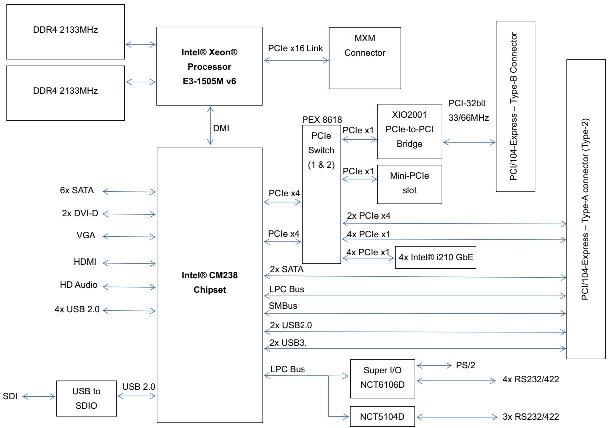
Figure 1-1: HPERC-KBL-M Block Diagram 4

Figure 1-2: HPERC-KBL-M Unit with Optional Accessories 6

Figure 2-1: Top and Front Views of “MH” Enclosure with Mounting Dimensions ....8

Figure 2-2: Top and Front Views of “MC” Enclosure with Mounting Dimensions ....9

Figure 2-3: Bottom View of "MC" Enclosure with Mounting Holes....10

Figure 2-4: Front View of HPERC-KBL-M I/O Panel 12

Figure 2-5: P2 and P3 Military Interface Connector Pin Locations 15

This page intentionally left blank.

# List of Tables

Table 1-1: HPERC-KBL-M Specifications .... 2

Table 1-2: System Power Requirements....5

Table 2-1: I/O Panel Connectors....13

Table 2-2: DB9 Male Connector Pin Definition....14

Table 2-3: GPIO Breakout Wires....14

Table 2-4: P2 Connector Pin Definitions and Signal Maps....16

Table 2-5: P3 Connector Pin Definitions and Signal Maps....19

This page intentionally left blank.

# 1 Introduction

# 1.1 About the HPERC-KBL-M

The HPERC products are intended for users of embedded systems requiring long life-cycles, configuration control, and ruggedness in hardened military packages. HPERC models feature Extreme Rugged computer boards available with varieties of processors and memory. An optional operating system (OS) can be pre-loaded onto an optional internal storage device (two 2.5" SSDs).

# 1.2 Using this Guide

This guide provides the most efficient way to set up your HPERC-KBL-M with your desired OS. The instructions provided in this guide include:

▶ Preparing to use the HPERC-KBL-M and inspecting the accessories
▶ Connecting peripherals to the HPERC-KBL-M
▶ Powering up the HPERC-KBL-M

Information not provided in this User's Guide includes:

▶ Board or Module specifications
▶ Board or Module header signals and descriptions
▶ Operating system programming or operating instructions

![The image displays a white document icon with a folded top-left corner. Faint grey horizontal lines run across the document. A large red checkmark is drawn over the document.](.hperc-kbl-m-50m-00048-1020-12/d61f531d967629a7ca9749d6dd28ad145522ab00025b0eeeb4f33fe008c31260.jpg)

NOTE:

Refer to OS manufacturers' manuals for instructions when using OS software.

# 1.3 Requirements

The following peripherals and devices are needed to make full use of the HPERC-KBL-M.

▶ Peripherals (user-provided):
▶ USB or PS/2 keyboard
▶ USB or PS/2 mouse
▷ Display monitor

![The image displays a white document icon featuring faint horizontal lines. A large, bold red checkmark is superimposed over the center of the page. The top-left corner of the paper is folded down.](.hperc-kbl-m-50m-00048-1020-12/8cb0abb9372ab52d0988a91ab2818aa99c5f3015f515ebef79ec30786dc645e0.jpg)

NOTE:

The items listed above are not available from ADLINK.

▶ Power Supply (optional):
▷ AC Adapter (with plug-type mating cord)

# 1.4 Specifications

Table 1-1: HPERC-KBL-M Specifications

<table><tr><td>VITA Standards</td><td>VITA 75</td></tr><tr><td rowspan="2">Mechanical</td><td>MC:Form Factor: VITA-75.22 Conductive Cold PlateDimensions: 223.65(L) x 177.80(W) x 98.70(H) mm (with mounting brackets)Weight: 4.7kg</td></tr><tr><td>MH:Form Factor: VITA-75 Finned Passive ConvectionDimensions: 304.80(L) x 150.00(W) x 129.95(H) mm (with mounting brackets)Weight: 5.6kg</td></tr><tr><td>Processor</td><td>Intel® Xeon® Processor E3-1505M v64C/8T Intel® Xeon® Processor E3-1505M v6, 3.00 GHz, 8MB Cache, TDP 45W</td></tr><tr><td>Chipset</td><td>Intel® CM238 Chipset</td></tr><tr><td>Host Memory</td><td>16GB dual channel DDR4-2400 DRAM with ECC, soldered onboard</td></tr><tr><td>BIOS</td><td>AMI EFI BIOS, 64Mbit SPI flash memory</td></tr><tr><td>Graphics</td><td>Intel® HD Graphics P6302x DVI and 1x VGA (3 simultaneous display outputs)</td></tr><tr><td>GPGPU</td><td>Optional:NVIDIA Quadro P1000/P2000 w/ 4GB GDDR5 memory in MXM slotNVIDIA Quadro T1000 w/ 4GB GDDR6 memory in MXM slot</td></tr><tr><td>Gigabit Ethernet</td><td>Four Intel® i210 10/100/1000 Ethernet ports</td></tr><tr><td>Serial Port</td><td>Seven RS-232/RS-422 serial ports</td></tr><tr><td>USB 2.0</td><td>Six USB 2.0 ports (500 mA)</td></tr><tr><td>PS/2</td><td>One PS/2 Keyboard portOne PS/2 Mouse port</td></tr><tr><td>SMBus</td><td>SMBus 2.0 supported</td></tr><tr><td>GPIO</td><td>Eight GPIO</td></tr><tr><td>Audio</td><td>High Definition Audio Controller (ALC262)1x amplified stereo output1x stereo input</td></tr><tr><td>TPM</td><td>Infineon SLB9665XT2.0 Module</td></tr><tr><td>Storage Interface</td><td>Two SATA 6 Gb/s ports for 2.5&quot; onboard drives (removable)One SDHC slot supports up to 32GB SDHC</td></tr><tr><td>RAID</td><td>Supports RAID 0/1 via Intel chipset</td></tr><tr><td>I/O Connector</td><td>MIL-DTL-38999 (uniquely-keyed)</td></tr><tr><td>Expansion Busses</td><td>MXM (PCIe x16 Gen3)PCI/104 Express® Type 2 (PCIe Gen2)PCI Express Mini Card (PCIe Gen2)</td></tr><tr><td>OS Compatibility</td><td>Microsoft Windows 10RHEL 7.0, RHEL 8.3, Ubuntu 14.04-4Other OS support by request</td></tr><tr><td>Power States</td><td>S0, S1, S3, S4</td></tr></table>

Table 1-1: HPERC-KBL-M Specifications

<table><tr><td rowspan="2">Operating Temperature</td><td>MC: Cold plate conduction, VITA 75.22 mountCPU Only: -40°C to +85°C at cold plate*With MXM-P1000/P2000: -40°C to +74°C at cold plate*With MXM T1000: -40°C to +71°C at cold plate**Note: Dependent on an external thermal solution design that maintains the temperature at any point on the cold plate surface within the indicated temperature range.</td></tr><tr><td>MH: Top-cover heatsink cooled (free air convection), VITA 75.21 mountCPU Only: -40°C to +75°C ambient*With MXM-P1000/P2000: -40°C to +70°C ambient (with 30 CFM airflow)With MXM T1000: -40°C to +69°C ambient (with 43.6 CFM airflow)</td></tr><tr><td>Storage Temperature</td><td>-40°C to +85°C</td></tr><tr><td>Power</td><td>18 to 36VDC input</td></tr><tr><td>Relative Humidity</td><td>95% at +60°C non-condensing</td></tr><tr><td colspan="2">Certifications</td></tr><tr><td>Temperature</td><td>MIL-STD-810G - 501.5 Procedure IIMIL-STD-810G - 502.5, Procedure 1 and 2</td></tr><tr><td>Immersion</td><td>IEC60529 Edition 2.2: 2013; IP67</td></tr><tr><td>Shock</td><td>MIL-STD-810G, Method 516.6, Procedure I (Functional Shock),Table 516.6-I (40 G for Ground Equipment)MIL-STD-810G, Method 516.6, Procedure V (Crash Hazard),Table 516.6-I (75 G for Crash Hazard Shock)</td></tr><tr><td>Vibration</td><td>MIL-STD-810G, Method 514.6, Table 514.6C-X,Category 9 - Helicopter vibration exposure (General)MIL-STD-810G, Method 514.6, Figure 514.6C-10,Category 11 - Rail cargo vibration exposure.MIL-STD-810G, Method 514.6, Figure 514.6D-9,Category 21 - Shipboard random vibration exposureMIL-STD-810G, Method 514.6, Table 514.6C-VI,Category 4 - Composite wheeled vehicle vibration exposure</td></tr><tr><td>EMI/EMC</td><td>MIL-STD-461F Certification: Ground Army, Aircraft, Navy complianceCE101: Navy ASW aircraft &amp; Army aircraft (incl. flight line, below 28V)CE102: Ground Army, Aircraft, NavyCS101: Ground Army, Aircraft, NavyCS115: Ground Army, Aircraft, NavyRE102: Air &amp; space (Fixed Wing External and Helicopters)RS101: Ground ArmyRS103: 100V/m (Ground Army, Ground Navy)RE101: Ground NavyCS106: Ground Army, Aircraft, Navy ( $V_{peak}$ =400V)CS114: Aircraft (external or safety critical) -Curve5CS116: Ground Army, Aircraft, Navy ( $I_{max}$ =10A)</td></tr><tr><td>Power</td><td>MIL-STD-704FMIL-STD-1275E</td></tr></table>

# 1.5 Block Diagram

![Here is an accurate and concise description of the flowchart, listing the blocks and their verbatim connections:\n\n**Top Section (Processor and Memory)**\n*   **Blocks:** Two 'DDR4 2133MHz' blocks, 'Intel® Xeon® Processor E3-1505M v6', 'MXM Connector'.\n*   **Connections:**\n    *   Both 'DDR4 2133MHz' blocks connect bidirectionally to the 'Intel® Xeon® Processor E3-1505M v6'.\n    *   'Intel® Xeon® Processor E3-1505M v6' connects bidirectionally to 'MXM Connector' via a 'PCIe x16 Link'.\n    *   'Intel® Xeon® Processor E3-1505M v6' connects bidirectionally to 'Intel® CM238 Chipset' via 'DMI'.\n\n**Left Side (Chipset Peripherals)**\n*   **Blocks:** 'Intel® CM238 Chipset', '6x SATA', '2x DVI-D', 'VGA', 'HDMI', 'HD Audio', '4x USB 2.0', 'USB to SDIO', 'SDI'.\n*   **Connections:**\n    *   'Intel® CM238 Chipset' connects bidirectionally to '6x SATA', '2x DVI-D', 'VGA', 'HDMI', 'HD Audio', and '4x USB 2.0'.\n    *   'USB to SDIO' connects bidirectionally to 'Intel® CM238 Chipset' via 'USB 2.0'.\n    *   'USB to SDIO' connects bidirectionally to 'SDI'.\n\n**Right Side (PCIe Switch and Expansion)**\n*   **Blocks:** 'PEX 8618 PCIe Switch (1 & 2)', 'XIO2001 PCIe-to-PCI Bridge', 'Mini-Pcie slot', '4x Intel® i210 GbE', 'PCI/104-Express – Type-B Connector', 'PCI/104-Express – Type-A connector (Type-2)'.\n*   **Connections:**\n    *   'Intel® CM238 Chipset' connects via two 'PCIe x4' lines to 'PEX 8618 PCIe Switch (1 & 2)'.\n    *   'PEX 8618 PCIe Switch (1 & 2)' connects bidirectionally to 'XIO2001 PCIe-to-PCI Bridge' via 'PCIe x1'.\n    *   'PEX 8618 PCIe Switch (1 & 2)' connects bidirectionally to 'Mini-Pcie slot' via 'PCIe x1'.\n    *   'PEX 8618 PCIe Switch (1 & 2)' connects bidirectionally to '4x Intel® i210 GbE' via '4x PCIe x1'.\n    *   'PEX 8618 PCIe Switch (1 & 2)' connects bidirectionally to 'PCI/104-Express – Type-B Connector' via '2x PCIe x4'.\n    *   'PEX 8618 PCIe Switch (1 & 2)' connects bidirectionally to 'PCI/104-Express – Type-A connector (Type-2)' via '4x PCIe x1'.\n    *   'XIO2001 PCIe-to-PCI Bridge' connects bidirectionally to 'PCI/104-Express – Type-B Connector' via 'PCI-32bit 33/66MHz'.\n    *   'Intel® CM238 Chipset' connects bidirectionally to 'PCI/104-Express – Type-A connector (Type-2)' via '2x SATA', 'LPC Bus', 'SMBus', '2x USB2.0', and '2x USB3.'.\n\n**Bottom Right (Super I/O)**\n*   **Blocks:** 'Super I/O NCT6106D', 'NCT5104D', 'PS/2', '4x RS232/422', '3x RS232/422'.\n*   **Connections:**\n    *   'Intel® CM238 Chipset' connects via 'LPC Bus' to both 'Super I/O NCT6106D' and 'NCT5104D'.\n    *   'Super I/O NCT6106D' connects bidirectionally to 'PS/2' and '4x RS232/422'.\n    *   'NCT5104D' connects bidirectionally to '3x RS232/422'.](.hperc-kbl-m-50m-00048-1020-12/d7acd830ab320fa482f00c300522a4c82d0c59d015f3713a685388370a14e848.jpg)

Figure 1-1: HPERC-KBL-M Block Diagram

# 1.6 Power Specifications

Table 1-2 lists the current and power draw of the HPERC-KBL-M, featuring the Intel® Xeon® Processor E3-1505M v6 (3.00GHz). Input power is +24 VDC regulated.

Table 1-2: System Power Requirements

<table><tr><td>Parameter</td><td>Current (Power)</td></tr><tr><td>Idle(Windows 10)</td><td>1.1A (26.4W)</td></tr><tr><td>Intel TA tool @100%(Windows 10)</td><td>3.16A (75.9W)</td></tr><tr><td>Inrush Current</td><td>1.5A (36W)</td></tr></table>

# 1.7 What's in the Box

Check the items in the shipping box for the HPERC-KBL-M Unit and optional accessories (sold separately).

![HPERC-KBL-MH\nCooling Fins\n(pre-installed on MH\nversion only)\nHPERC-KBL-MC\nMounting Brackets\nCold Plate\n(pre-installed on MC\nversion, only)](.hperc-kbl-m-50m-00048-1020-12/ce9c94e755b6c21cee0eb28c23035b83e8b03149c1a56141cfa23adcc0feb459.jpg)

HPERC Accessories (sold separately)
![DC Cable Connector\nAC Adapter\nBreakout Cables\nAC Mating Cable\nBreakout Cables](.hperc-kbl-m-50m-00048-1020-12/0bbee0e60742ca7a70c754bbc5d39dc1ea83bb695fee2be031ed6ff5ba71f6cd.jpg)

Figure 1-2: HPERC-KBL-M Unit with Optional Accessories

# 2 Getting Started

# 2.1 Preparation

Follow the setup steps in this section in the order listed. Skip any steps that do not apply to your application.

▶ Verify the contents of the shipping box are the same as your HPERC-KBL-M order.
▶ If anything is missing or damaged, call your sales representative. Refer to the Getting Service chapter for contact information.

# 2.2 Setting Up the Work Space

![The image displays a white document icon with faint horizontal grey lines, overlaid with a large red checkmark. Below the icon, the text 'NOTE:' appears in black capital letters.](.hperc-kbl-m-50m-00048-1020-12/e97dbd17435d16d250cf5441598dee2fe1bd7eb8908eb7ba9ffbd22de1b11a5b.jpg)

To prevent damage to the HPERC-KBL-M, ensure sufficient clearance exists around the cooling solution for unrestricted airflow.

The air temperature inside the enclosure could rise above the specified operating temperature limits if the airflow through the cooling solution is restricted.

<table><tr><td>Select workbench location.</td><td>The workbench location should be a flat clean surface for setup and operation (including the connection of any external peripherals and optional devices).Ensure sufficient airflow clearance exists around the complete enclosure.</td></tr><tr><td>Unpack HPERC-KBL-M.</td><td>Remove the HPERC-KBL-M from its shipping container and place it on a flat work surface.The HPERC-KBL-M enclosure combined with CPU, storage (SSD), and the desired OS form a complete system, ready for operation.</td></tr></table>

# 2.3 Mounting the Enclosure

Install mounting screws (not included) for surface or wall mounting to the mounting brackets of the HPERC-KBL-M. Refer to Figure 2-1 and Figure 2-2 for the mounting hole locations of your model.

![The image features a graphic icon of a document. It depicts a white sheet of paper with faint horizontal lines running across it. Superimposed diagonally over the center of the paper is a large, bold, red checkmark. Below the paper graphic, the word 'NOTE:' is printed in black, uppercase letters.](.hperc-kbl-m-50m-00048-1020-12/8750d1852bb30c09c4a8be11a46ef3d90b9f6827ea664deb5bedf0f3849e6518.jpg)

There are no limitations to the mounting orientation of the device.

Torque Values

<table><tr><td>Nominal Diameter</td><td>Material: Stainless Steel A2-70 and A4-70</td><td>Material: Stainless Steel A2-80 and A4-80</td><td>Material: SCM3 (SCM435) Strength Grade: 12.9</td></tr><tr><td>M6 (HPERC-KBL-MC)</td><td>7.6 Nm</td><td>11.1 Nm</td><td>13.83 Nm</td></tr><tr><td>M8 (HPERC-KBL-MH)</td><td>18.4 Nm</td><td>26.7 Nm</td><td>33.34 Nm</td></tr></table>

![(12.000 ±0.022)\n304.80 ±0.55\n(8.000 ±0.006)\n203.20 ±0.15\n(1.000 ±0.008)\n25.4 ±0.2\n(2.000 ±0.016)\n50.8 ±0.4\n(2.756 ±0.008)\n70 ±0.2\n(1.575)\n40\n(1.000 ±0.008)\n25.4 ±0.2\n(5.906 ±0.016)\n150 ±0.4\n(4.331 ±0.014)\n110 ±0.35\n(0.374 ±0.008)\nØ9.5 ±0.2\n(8.587 ±0.020)\n218.1 ±0.5\n(8.805 ±0.026)\n223.65 ±0.65\n(10.000 ±0.022)\n254 ±0.55](.hperc-kbl-m-50m-00048-1020-12/10c9b1737e881436863e795311e382ef39bae46b1a21b8a5f1ade882254f0cfe.jpg)

![ADLINK\nTECHNOLOGY INC.\n(2.433 ±0.014)\n61.80 ±0.35\n(1.410 ±0.014)\n35.82 ±0.35\n(2.953 ±0.014)\n75 ±0.35\n(4.495 ±0.014)\n114.18 ±0.35\n(2.200 ±0.014)\n55.87 ±0.35\n+0.022\n-0.012\n+0.55\n129.95 -0.30\nDimensions in mm (inches)](.hperc-kbl-m-50m-00048-1020-12/fa050267cdf9dcb634cb7a8f51105e6ddbe9dc22b59e82f0a3d9db260463dd97.jpg)

Figure 2-1: Top and Front Views of “MH” Enclosure with Mounting Dimensions

![| Component | Dimension (±) |\n| :--- | :--- |\n| (7.000 ± 0.014) | 177.80 ± 0.35 |\n| (6.500 ± 0.008) | 165.1 ± 0.2 |\n| (5.906 ± 0.008) | 150 ± 0.2 |\n| (8.805 ± 0.026) | 223.65 ± 0.65 |\n| (2.000 ± 0.008) | 50.8 ± 0.2 |\n| (6.000 ± 0.008) | 152.4 ± 0.2 |\n| (8.587 ± 0.020) | 203.2 ± 0.2 |\n| (8.587 ± 0.020) | 218.1 ± 0.5 |\n| (0.547) | 13.9 |\nThe label 'ADLINK TECHNOLOGY INC.' is centered within the diagram, but it is not part of the chart's data series or axes.](.hperc-kbl-m-50m-00048-1020-12/75b652d464bf83f219363fac81ccea93b44d73ef2e77ef73ace10f6c79a764b9.jpg)

![(1.453 ±0.014)\n36.90 ±0.35\n(0.354)\n9\n(1.410 ±0.014)\n35.82 ±0.35\n(2.953 ±0.014)\n75 ±0.35\n(4.495 ±0.014)\n114.18 ±0.35\nP1\nP2\nP3\n+0.022\n-0.012\n+0.55\n-0.30\n3.886\n98.70\n1.686 ±0.014\n42.83 ±0.35\nDimensions in mm (inches)](.hperc-kbl-m-50m-00048-1020-12/7e4694edaa5ad16816d3396d7415b69bddf3a86285186f9ac319133e48bfaccb.jpg)

Figure 2-2: Top and Front Views of “MC” Enclosure with Mounting Dimensions

<table><tr><td>Optional mounting points for surface/wall mounting or heat sink (HPERC-KBL-MC only)</td><td>• Mounting holes “A” and “B” are shown below in Figure 2-3. Note the recommended torque values and maximum depth of hole “B”.</td></tr></table>

Mounting Hole "A" Size: M4 threaded

Recommended Torque: 30 Kgf-cm (2.85 N-m)

Mounting Hole "B" Size: M4 threaded, max. depth 7mm

Recommended Torque: 41 Kgf-cm (4 N-m)

![| Dimension | Value        |\n| --------- | ------------ |\n| (2.126 ± 0.008) | 54 ± 0.20   |\n| (1.398 ± 0.008) | 35.5 ± 0.2   |\n| (2.287 ± 0.008) | 58.1 ± 0.2   |\n| (6.100 ± 0.008) | 154.94 ± 0.20 |\n| (4.022 ± 0.008) | 194.2 ± 0.2   |\n| (2.854 ± 0.008) | 72.5 ± 0.2    |\n| (1.723 ± 0.008) | 43.78 ± 0.20  |\n| (1.398 ± 0.008) | 35.5 ± 0.2    |\n| (3.500 ± 0.008) | 88.9 ± 0.2    |\n| (5.138 ± 0.008) | 130.5 ± 0.2   |\n| (5.843 ± 0.008) | 148.4 ± 0.2   |\n| (2.000 ± 0.008) | 50.8 ± 0.2    |\n| (2.000 ± 0.008) | 574.80 ± 7.87 |\n| (6.173 ± 0.008) | 156.8 ± 0.2   |\n| (14.6 ± 0.2    | 146 ± 0.2     |](.hperc-kbl-m-50m-00048-1020-12/7cde64c2946631575148b147fe7ecbe4c83160cfee6c9dcf8eec9b86e10a43e7.jpg)

Figure 2-3: Bottom View of “MC” Enclosure with Mounting Holes

# 2.4 Connecting Peripherals

<table><tr><td>Connect the appropriate military breakout cable to the corresponding HPERC-KBL-M military connector. See Figure 1-2 for illustrations of cables. See Figure 2-4 for locations of the HPERC-KBL-M military connectors.</td><td>·Refer to Figure 2-4 for locations and descriptions of the connectors before making connections or powering on the HPERC-KBL-M.</td></tr><tr><td>&lt;img src="images/a7ef2d6cb12a9e3a3454a8067e548a50be5453cc3cfc7739d43418d47993f075.jpg"/&gt;</td><td>·Connect the USB or PS2 keyboard to the corresponding connector on the corresponding breakout cable.</td></tr><tr><td>&lt;img src="images/1ea6766142ebfe26741551d6ae318ac38cc05b67c18fe38ad4906b00d1cbad48.jpg"/&gt;</td><td>·Connect the USB or PS2 mouse to the appropriate connector on the corresponding breakout cable.</td></tr><tr><td>&lt;img src="images/66f38baf0d2c2a4266010996f29446192c906e8b969b8aad1f1b1843faf50787.jpg"/&gt;</td><td>·Connect the display to the appropriate connector on the corresponding breakout cable.</td></tr></table>

![The image displays an icon of a white document with a folded top-right corner. Faint horizontal lines run across the page, suggesting text. A large, bold red checkmark is superimposed over the center of the document. There is no text in the image.](.hperc-kbl-m-50m-00048-1020-12/f8f3b2e08e6d6df636216bdc2fde00751cd5d942a4b676e3f756bf34f79370ac.jpg)
NOTE:

To connect an external storage or CD drive to the HPERC-KBL-M, use one of the USB or SATA ports to connect the device.

# 2.5 Front Panel Connectors & LEDs
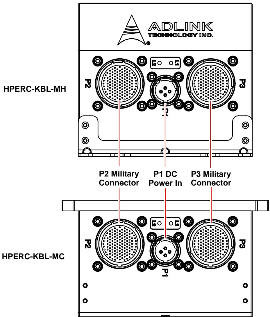
![ADLINK\nTECHNOLOGY INC.\nHPERC-KBL-MH\nP2\nP3\nP2 Military\nConnector P1 DC\nPower In P3 Military\nConnector\nHPERC-KBL-MC](.hperc-kbl-m-50m-00048-1020-12/445432d5f014495ca86bf5ca350062f8fb8d7222a6c0e0f08a00da2a4900b2f5.jpg)

Figure 2-4: Front View of HPERC-KBL-M I/O Panel

# Connector & LED Descriptions

Refer to Figure 2-4 for connector locations.

Table 2-1: I/O Panel Connectors

<table><tr><td>Connector</td><td>Description</td></tr><tr><td>P1: DC Power In&lt;img src="images/4b5456e9e42e5d52f59022b36e294ced6e13fba46618df3a6e6a98e2d449cbf9.jpg"/&gt;</td><td>This Military Power connector accepts DC voltages from an external source.Note: This connector is manufactured by Amphenol.</td></tr><tr><td>P2: Military Connector</td><td>This military connector provides signals for Ethernet Ports, USB 2.0, Serial Ports, Reset Switch, Ethernet LEDs, and UNDIO.</td></tr><tr><td>P3: Military Connector</td><td>This military connector provides signals for VGA, Ethernet LEDs, Ethernet Ports, Serial Ports, PS/2 Keyboard and Mouse, and RCA Jack.</td></tr><tr><td>L1/L2: Status LEDs</td><td>The functionality of the status LEDs is described in the table below</td></tr></table>

<table><tr><td>Status</td><td>L1 LED</td><td>L2 LED</td></tr><tr><td>Power On</td><td>Steady orange, then steady red</td><td>Steady orange, then steady green</td></tr><tr><td>Hardware Reset Button Pressed</td><td>No change (steady red)</td><td>Blinking orange, then steady green</td></tr><tr><td>Hardware Power Button Pressed</td><td>Orange to steady red</td><td>Steady green</td></tr><tr><td>OS Power Off</td><td>Red to steady orange</td><td>Steady green</td></tr></table>

# 2.6 Breakout Cable Descriptions

RS-232/RS-422 Serial Ports

![① ② ③ ④ ⑤\n⑥ ⑦ ⑧ ⑨](.hperc-kbl-m-50m-00048-1020-12/e939036baba499b8d695e3798288133bf12d4505ddb8db58ab0afd243f4b5d87.jpg)

Table 2-2: DB9 Male Connector Pin Definition

<table><tr><td>Pin #</td><td>RS232</td><td>RS422</td></tr><tr><td>1</td><td>NC</td><td>NC</td></tr><tr><td>2</td><td>—</td><td>RXp</td></tr><tr><td>3</td><td>—</td><td>TXp</td></tr><tr><td>4</td><td>NC</td><td>NC</td></tr><tr><td>5</td><td>NC</td><td>NC</td></tr><tr><td>6</td><td>NC</td><td>NC</td></tr><tr><td>7</td><td>TX</td><td>TXn</td></tr><tr><td>8</td><td>RX</td><td>RXn</td></tr><tr><td>9</td><td>NC</td><td>NC</td></tr></table>

# GPIO

Table 2-3: GPIO Breakout Wires

<table><tr><td>Function/Label</td><td>Pin</td><td>Signal</td></tr><tr><td>GPIO1</td><td>P2-45</td><td>UDNIO13</td></tr><tr><td>GPIO2</td><td>P2-46</td><td>UDNIO14</td></tr><tr><td>GPIO3</td><td>P2-48</td><td>UDNIO15</td></tr><tr><td>GPIO4</td><td>P2-49</td><td>UDNIO16</td></tr><tr><td>GPIO5</td><td>P2-51</td><td>UDNIO17</td></tr><tr><td>GPIO6</td><td>P2-52</td><td>UDNIO18</td></tr><tr><td>GPIO7</td><td>P2-54</td><td>UDNIO19</td></tr><tr><td>GPIO8</td><td>P2-55</td><td>UDNIO20</td></tr></table>

# 2.7 P2 and P3 Military Connectors

The following two tables define the signals and signal maps of the two military I/O connectors (P2 and P3) on the HPERC-KBL-M. Each table lists the P2 or P3 pin numbers, the signal names and descriptions. Figure 2-5 provides the number and location of each pin on the two military connectors.

# 2.7.1 P2 and P3 Connector Locations

![| Position | Value |\n|---|---|\n| 1 | 1 |\n| 2 | 2 |\n| 3 | 3 |\n| 4 | 4 |\n| 5 | 5 |\n| 6 | 6 |\n| 7 | 7 |\n| 8 | 8 |\n| 9 | 9 |\n| 10 | 10 |\n| 11 | 11 |\n| 12 | 12 |\n| 13 | 13 |\n| 14 | 14 |\n| 15 | 15 |\n| 16 | 16 |\n| 17 | 17 |\n| 18 | 18 |\n| 19 | 19 |\n| 20 | 20 |\n| 21 | 21 |\n| 22 | 22 |\n| 23 | 23 |\n| 24 | 24 |\n| 25 | 25 |\n| 26 | 26 |\n| 27 | 27 |\n| 28 | 28 |\n| 29 | 29 |\n| 30 | 30 |\n| 31 | 31 |\n| 32 | 32 |\n| 33 | 33 |\n| 34 | 34 |\n| 35 | 35 |\n| 36 | 36 |\n| 37 | 37 |\n| 38 | 38 |\n| 39 | 39 |\n| 40 | 40 |\n| 41 | 41 |\n| 42 | 42 |\n| 43 | 43 |\n| 44 | 44 |\n| 45 | 45 |\n| 46 | 46 |\n| 47 | 47 |\n| 48 | 48 |\n| 49 | 49 |\n| 50 | 50 |\n| 51 | 51 |\n| 52 | 52 |\n| 53 | 53 |\n| 54 | 54 |\n| 55 | 55 |\n| 56 | 56 |\n| 57 | 57 |\n| 58 | 58 |\n| 59 | 59 |\n| 60 | 60 |\n| 61 | 61 |\n| 62 | 62 |\n| 63 | 63 |\n| 64 | 64 |\n| 65 | 65 |\n| 66 | 66 |\n| 67 | 67 |\n| 68 | 68 |\n| 69 | 69 |\n| 70 | 70 |\n| 71 | nan |\n| 72 | nan |\n| 73 | nan |\n| 74 | nan |\n| 75 | nan |\n| 76 | nan |\n| 77 | nan |\n| 78 | nan |\n| 79 | nan |\n| 80 | nan |\n| 81 | nan |\n| 82 | nan |\n| 83 | nan |\n| 84 | nan |\n| 85 | nan |\n| 86 | nan |\n| 87 | nan |\n| 88 | nan |\n| 89 | nan |\n| 90 | nan |\n| 91 | nan |\n| 92 | nan |\n| 93 | nan |\n| 94 | nan |\n| 95 | nan |\n| 96 | nan |\n| 97 | nan |\n| 98 | nan |\n| 99 | nan |\n|100 | nan |\n|101 | nan |\n|102 | nan |\n|103 | nan |\n|104 | nan |\n|105 | nan |\n|106 | nan |\n|107 | nan |\n|108 | nan |\n|109 | nan |\n|110 | nan |\n|111 | nan |\n|112 | nan |\n|113 | nan |\n|114 | nan |\n|115 | nan |\n|116 | nan |\n|117 | nan |\n|118 | nan |\n|119 | nan |\n|120 | nan |\n|121 | nan |\n|122 | nan |\n|123 | nan |\n|124 | nan |\n|125 | nan |\n|126 | nan |\n|127 | nan |\n|128 | nan |\n|129 | nan |\n|130 | nan |\nThe values are estimated based on the provided code and are not explicitly provided in the original image. The numbers in the 'Values' column are estimated based on the 'Value' column.](.hperc-kbl-m-50m-00048-1020-12/3456822c7bbf53b1de3094b5c8294b57e0ac84d4529f0a0fb97e7c736ef97583.jpg)

Figure 2-5: P2 and P3 Military Interface Connector Pin Locations

# 2.7.2 P2 Pin Definitions

Table 2-4: P2 Connector Pin Definitions and Signal Maps

<table><tr><td>P2 Pin</td><td>Interface</td><td>Signal</td><td>Signal Description</td></tr><tr><td>1</td><td>Gigabit Ethernet 1</td><td>GbE2_MDI0_P</td><td>Ethernet10 MDI0 Positive</td></tr><tr><td>2</td><td>Gigabit Ethernet 1</td><td>GbE2_MDI1_N</td><td>Ethernet1 MDI1 Negative</td></tr><tr><td>3</td><td>Gigabit Ethernet 1</td><td>GbE2_MDI1_P</td><td>Ethernet1 MDI1 Positive</td></tr><tr><td>4</td><td>Ground</td><td>GND</td><td>Ground</td></tr><tr><td>5</td><td>Gigabit Ethernet 1</td><td>GbE2_MDI2_N</td><td>Ethernet1 MDI2 Negative</td></tr><tr><td>6</td><td>Gigabit Ethernet 1</td><td>GbE2_MDI2_P</td><td>Ethernet1 MDI2 Positive</td></tr><tr><td>7</td><td>Gigabit Ethernet 1</td><td>GbE2_MDI3_N</td><td>Ethernet1 MDI3 Negative</td></tr><tr><td>8</td><td>Gigabit Ethernet 1</td><td>GbE2_MDI0_N</td><td>Ethernet1 MDI0 Negative</td></tr><tr><td>14</td><td>Gigabit Ethernet 1</td><td>GbE2_MDI3_P</td><td>Ethernet1 MDI3 Positive</td></tr><tr><td>9</td><td>USB 2.0, Port 4</td><td>USB_P4</td><td>Data Positive</td></tr><tr><td>10</td><td>USB 2.0, Port 4</td><td>USB_N4</td><td>Data Negative</td></tr><tr><td>11</td><td>USB 2.0, Port 4</td><td>USB_GND4</td><td>Ground</td></tr><tr><td>12</td><td>USB 2.0, Port 5</td><td>USB_P5</td><td>Data Positive</td></tr><tr><td>13</td><td>USB 2.0, Port 5</td><td>USB_N5</td><td>Data Negative</td></tr><tr><td>27</td><td>USB 2.0, Port 5</td><td>USB_GND5</td><td>Ground</td></tr><tr><td>15</td><td>USB 2.0, Port 4</td><td>P5V_USB4</td><td>+5 Volts Power</td></tr><tr><td>16</td><td>USB 2.0, Port 5</td><td>P5V_USB5</td><td>+5 Volts Power</td></tr><tr><td>17</td><td>Serial 4</td><td>RS422_TX4_N</td><td>Transmit Data Negative</td></tr><tr><td>18</td><td>Serial 4</td><td>RS422_TX4_P</td><td>Transmit Data Positive</td></tr><tr><td>19</td><td>Serial 4</td><td>RS422_RX4_N</td><td>Receive Data Negative</td></tr><tr><td>20</td><td>Serial 4</td><td>RS422_RX4_P</td><td>Receive Data Positive</td></tr><tr><td>21</td><td>Serial 6</td><td>RS422_RX6_N</td><td>Receive Data Negative</td></tr><tr><td>22</td><td>Serial 6</td><td>RS422_RX6_P</td><td>Receive Data Positive</td></tr><tr><td>23</td><td>Serial 6</td><td>RS422_TX6_N</td><td>Transmit Data Negative</td></tr><tr><td>24</td><td>Serial 6</td><td>RS422_TX6_P</td><td>Transmit Data Positive</td></tr><tr><td>25</td><td>NC</td><td>NC</td><td>Not Connected</td></tr><tr><td>26</td><td>NC</td><td>NC</td><td>Not Connected</td></tr><tr><td>27</td><td>Ground</td><td>GND</td><td>Ground</td></tr><tr><td>28</td><td>USB 2.0, Port 8</td><td>USB_PWR8</td><td>USB 2.0 +5V Power</td></tr><tr><td>30</td><td>USB 2.0, Port 8</td><td>USB_P8</td><td>USB 2.0 Data Positive</td></tr><tr><td>31</td><td>USB 2.0, Port 8</td><td>USB_N8</td><td>USB 2.0 Data Negative</td></tr><tr><td>32</td><td>USB 2.0, Port 8</td><td>USB_GND8</td><td>USB 2.0 Ground</td></tr><tr><td>29</td><td>Reset Switch</td><td>RESET#_HDR</td><td>Resets the system</td></tr><tr><td>38</td><td>Ground</td><td>GND</td><td>Ground</td></tr><tr><td>33</td><td>Control/Indicator</td><td>PWR_LED</td><td>Power LED (330ohm to +5V)</td></tr><tr><td>44</td><td>Ground</td><td>GND</td><td>Ground</td></tr><tr><td>34</td><td>Control/Indicator</td><td>PCIe_ETH_2/5_LED1</td><td>Ethernet LED</td></tr><tr><td>44</td><td>Ground</td><td>GND</td><td>Ground</td></tr><tr><td>35</td><td>NC</td><td>NC</td><td>Not Connected</td></tr><tr><td>44</td><td>Ground</td><td>GND</td><td>Ground</td></tr><tr><td>36</td><td>Control/Indicator</td><td>HPOUT_R</td><td>Audio Right</td></tr></table>

Table 2-4: P2 Connector Pin Definitions and Signal Maps

<table><tr><td>P2 Pin</td><td>Interface</td><td>Signal</td><td>Signal Description</td></tr><tr><td>37</td><td>Control/Indicator</td><td>HPOUT_L</td><td>Audio Left</td></tr><tr><td>38</td><td>Ground</td><td>GND</td><td>Ground</td></tr><tr><td>39</td><td>NC</td><td>NC</td><td>Not Connected</td></tr><tr><td>40</td><td>NC</td><td>NC</td><td>Not Connected</td></tr><tr><td>38</td><td>Ground</td><td>GND</td><td>Ground</td></tr><tr><td>41</td><td>Ground</td><td>GND</td><td>Ground</td></tr><tr><td>42</td><td>User Defined IO</td><td>UDNIO11</td><td>User Input/Output Port 11</td></tr><tr><td>43</td><td>User Defined IO</td><td>UDNIO12</td><td>User Input/Output Port 12</td></tr><tr><td>38</td><td>Ground</td><td>GND</td><td>Ground</td></tr><tr><td>44</td><td>Ground</td><td>GND</td><td>Ground</td></tr><tr><td>45</td><td>User Defined IO</td><td>UDNIO13</td><td>User Input/Output Port 13</td></tr><tr><td>46</td><td>User Defined IO</td><td>UDNIO14</td><td>User Input/Output Port 14</td></tr><tr><td>38</td><td>Ground</td><td>GND</td><td>Ground</td></tr><tr><td>47</td><td>Ground</td><td>GND</td><td>Ground</td></tr><tr><td>48</td><td>User Defined IO</td><td>UDNIO15</td><td>User Input/Output Port 15</td></tr><tr><td>49</td><td>User Defined IO</td><td>UDNIO16</td><td>User Input/Output Port 16</td></tr><tr><td>50</td><td>Ground</td><td>GND</td><td>Ground</td></tr><tr><td>51</td><td>User Defined IO</td><td>UDNIO17</td><td>User Input/Output Port 17</td></tr><tr><td>52</td><td>User Defined IO</td><td>UDNIO18</td><td>User Input/Output Port 18</td></tr><tr><td>53</td><td>Ground</td><td>GND</td><td>Ground</td></tr><tr><td>54</td><td>User Defined IO</td><td>UDNIO19</td><td>User Input/Output Port 19</td></tr><tr><td>55</td><td>User Defined IO</td><td>UDNIO20</td><td>User Input/Output Port 20</td></tr><tr><td>56</td><td>Ground</td><td>GND</td><td>Ground</td></tr><tr><td>57-81</td><td>NC</td><td>NA</td><td>NA</td></tr><tr><td>71</td><td>User Defined IO</td><td>UDNIO5</td><td>User Input/Output Port 5</td></tr><tr><td>72</td><td>User Defined IO</td><td>UDNIO6</td><td>User Input/Output Port 6</td></tr><tr><td>73</td><td>Ground</td><td>GND</td><td>Ground</td></tr><tr><td>74</td><td>User Defined IO</td><td>UDNIO7</td><td>User Input/Output Port 7</td></tr><tr><td>75</td><td>User Defined IO</td><td>UDNIO8</td><td>User Input/Output Port 8</td></tr><tr><td>76</td><td>Ground</td><td>GND</td><td>Ground</td></tr><tr><td>77</td><td>User Defined IO</td><td>UDNIO9</td><td>User Input/Output Port 9</td></tr><tr><td>78</td><td>User Defined IO</td><td>UDNIO10</td><td>User Input/Output Port 10</td></tr><tr><td>79</td><td>Ground</td><td>GND</td><td>Ground</td></tr><tr><td>82</td><td>Control/Indicator</td><td>LINE_IN_R</td><td>Audio In Right Channel</td></tr><tr><td>83</td><td>Control/Indicator</td><td>LINE_IN_L</td><td>Audio In Left Channel</td></tr><tr><td>84</td><td>NC</td><td>NC</td><td>NC</td></tr><tr><td>85</td><td>Ground</td><td>AGND</td><td>Analog Ground</td></tr><tr><td>86</td><td>Ground</td><td>AGND</td><td>Analog Ground</td></tr><tr><td>87</td><td>Ground</td><td>GND</td><td>Ground</td></tr><tr><td>88</td><td>User Defined IO</td><td>UDNIO1</td><td>User Input/Output Port 1</td></tr><tr><td>89</td><td>User Defined IO</td><td>UDNIO2</td><td>User Input/Output Port 2</td></tr><tr><td>90</td><td>Ground</td><td>GND</td><td>Ground</td></tr><tr><td>91</td><td>User Defined IO</td><td>UDNIO3</td><td>User Input/Output Port 3</td></tr></table>

Table 2-4: P2 Connector Pin Definitions and Signal Maps

<table><tr><td>P2 Pin</td><td>Interface</td><td>Signal</td><td>Signal Description</td></tr><tr><td>92</td><td>User Defined IO</td><td>UDNIO4</td><td>User Input/Output Port 4</td></tr><tr><td>93</td><td>Ground</td><td>GND</td><td>Ground</td></tr><tr><td>94</td><td>NC</td><td>NC</td><td>Not Connected</td></tr><tr><td>95</td><td>NC</td><td>NC</td><td>Not Connected</td></tr><tr><td>96</td><td>Ground</td><td>GND</td><td>Ground</td></tr><tr><td>98</td><td>Power Switch</td><td>PWERBTN_HDR</td><td>Powers on the system</td></tr><tr><td>97</td><td>USB 2.0, Port 9</td><td>USB_PWR9</td><td>USB 2.0 +5V Power</td></tr><tr><td>99</td><td>USB 2.0, Port 9</td><td>USB_N9</td><td>USB 2.0 Data Negative</td></tr><tr><td>100</td><td>USB 2.0, Port 9</td><td>USB_P9</td><td>USB 2.0 Data Positive</td></tr><tr><td>101</td><td>Ground</td><td>GND</td><td>Ground</td></tr><tr><td>102</td><td>Control/Indicator</td><td>SATA_LED#</td><td>SATA LED</td></tr><tr><td>101</td><td>Ground</td><td>GND</td><td>Ground</td></tr><tr><td>103</td><td>NC</td><td>NC</td><td>NC</td></tr><tr><td>101</td><td>Ground</td><td>GND</td><td>Ground</td></tr><tr><td>104</td><td>Control/Indicator</td><td>ERASE- L</td><td>GPIO Signal for SSD Secure Erase</td></tr><tr><td>101</td><td>Ground</td><td>GND</td><td>Ground</td></tr><tr><td>105</td><td>Power</td><td>P3V3_S</td><td>+3.3 Volts Standby</td></tr><tr><td>106</td><td>Power</td><td>P3V3_S</td><td>+3.3 Volts Standby</td></tr><tr><td>107</td><td>Serial 5</td><td>RS422_TX5_N</td><td>Transmit Data Negative</td></tr><tr><td>108</td><td>Serial 5</td><td>RS422_TX5_P</td><td>Transmit Data Positive</td></tr><tr><td>109</td><td>Serial 5</td><td>RS422_RX5_N</td><td>Receive Data Negative</td></tr><tr><td>110</td><td>Serial 5</td><td>RS422_RX5_P</td><td>Receive Data Positive</td></tr><tr><td>111</td><td>Serial 7</td><td>RS422_TX7_N</td><td>Transmit Data Negative</td></tr><tr><td>112</td><td>Serial 7</td><td>RS422_TX7_P</td><td>Transmit Data Positive</td></tr><tr><td>113</td><td>Serial 7</td><td>RS422_RX7_N</td><td>Receive Data Negative</td></tr><tr><td>114</td><td>Serial 7</td><td>RS422_RX7_P</td><td>Receive Data Positive</td></tr><tr><td>116-120</td><td>NC</td><td>NA</td><td>NA</td></tr><tr><td>115</td><td>Serial 0</td><td>RS422_TX0_N</td><td>Transmit Data Negative</td></tr><tr><td>122</td><td>Serial 0</td><td>RS422_TX0_P</td><td>Transmit Data Positive</td></tr><tr><td>123</td><td>Serial 0</td><td>RS422_RX0_N</td><td>Receive Data Negative</td></tr><tr><td>124</td><td>Serial 0</td><td>RS422_RX0_P</td><td>Receive Data Positive</td></tr><tr><td>125</td><td>Ground</td><td>GND</td><td>Ground</td></tr><tr><td>126</td><td>Serial 2</td><td>RS422_TX2_N</td><td>Transmit Data Negative</td></tr><tr><td>127</td><td>Serial 2</td><td>RS422_TX2_P</td><td>Transmit Data Positive</td></tr><tr><td>128</td><td>Serial 2</td><td>RS422_RX2_N</td><td>Receive Data Negative</td></tr><tr><td>121</td><td>Serial 2</td><td>RS422_RX2_P</td><td>Receive Data Positive</td></tr></table>

# 2.7.3 P3 Pin Definitions

Table 2-5: P3 Connector Pin Definitions and Signal Maps

<table><tr><td>P3 Pin</td><td>Interface</td><td>Signal</td><td>Signal Description</td></tr><tr><td>1</td><td>VGA</td><td>VGA_VSYNC</td><td>Vertical Sync</td></tr><tr><td>2</td><td>Ground</td><td>GND</td><td>Ground</td></tr><tr><td>33</td><td>Ground</td><td>GND</td><td>Ground</td></tr><tr><td>3</td><td>VGA</td><td>VGA_DDC_SCL</td><td>Display Data Channel - Serial Clock</td></tr><tr><td>4</td><td>VGA</td><td>VGA_DDC_SDA</td><td>Display Data Channel - Serial Data</td></tr><tr><td>5</td><td>Ground</td><td>GND</td><td>Ground</td></tr><tr><td>6</td><td>VGA</td><td>RED</td><td>Red Analog Output</td></tr><tr><td>18</td><td>Ground</td><td>GND</td><td>Ground</td></tr><tr><td>7</td><td>VGA</td><td>GREEN</td><td>Green Analog Output</td></tr><tr><td>21</td><td>Ground</td><td>GND</td><td>Ground</td></tr><tr><td>14</td><td>VGA</td><td>BLUE</td><td>Blue Analog Output</td></tr><tr><td>30</td><td>Ground</td><td>GND</td><td>Ground</td></tr><tr><td>8</td><td>VGA</td><td>HSYNC</td><td>Horizontal Sync</td></tr><tr><td>9</td><td>NC</td><td>NC</td><td>Not Connected</td></tr><tr><td>10</td><td>NC</td><td>NC</td><td>Not Connected</td></tr><tr><td>11</td><td>Ground</td><td>GND</td><td>Ground</td></tr><tr><td>12</td><td>Power</td><td>P3V3_S</td><td>+3.3 Volts Standby</td></tr><tr><td>13</td><td>Power</td><td>P3V3_S</td><td>+3.3 Volts Standby</td></tr><tr><td>15</td><td>Power</td><td>P3V3_S</td><td>+3.3 Volts Standby</td></tr><tr><td>38</td><td>Ground</td><td>GND</td><td>Ground</td></tr><tr><td>24</td><td>Control/Indicator</td><td>PCIe_ETH_5/5_LED1</td><td>Ethernet LED</td></tr><tr><td>114</td><td>Control/Indicator</td><td>PCIe_ETH_4/5_LED1</td><td>Ethernet LED</td></tr><tr><td>121</td><td>Control/Indicator</td><td>PCIe_ETH_3/5_LED1</td><td>Ethernet LED</td></tr><tr><td>16</td><td>Gigabit Ethernet 4</td><td>GbE5_MDI0_N</td><td>Ethernet4 MDI0 Negative</td></tr><tr><td>17</td><td>Gigabit Ethernet 4</td><td>GbE5_MDI0_P</td><td>Ethernet4 MDI0 Positive</td></tr><tr><td>18</td><td>Ground</td><td>GND</td><td>Ground</td></tr><tr><td>19</td><td>Gigabit Ethernet 4</td><td>GbE5_MDI1_N</td><td>Ethernet4 MDI1 Negative</td></tr><tr><td>20</td><td>Gigabit Ethernet 4</td><td>GbE5_MDI1_P</td><td>Ethernet4 MDI1 Positive</td></tr><tr><td>21</td><td>Ground</td><td>GND</td><td>Ground</td></tr><tr><td>22</td><td>Gigabit Ethernet 4</td><td>GbE5_MDI2_N</td><td>Ethernet4 MDI2 Negative</td></tr><tr><td>23</td><td>Gigabit Ethernet 4</td><td>GbE5_MDI2_P</td><td>Ethernet4 MDI2 Positive</td></tr><tr><td>100</td><td>Gigabit Ethernet 4</td><td>GbE5_MDI3_N</td><td>Ethernet4 MDI3 Negative</td></tr><tr><td>101</td><td>Gigabit Ethernet 4</td><td>GbE5_MDI3_P</td><td>Ethernet4 MDI3 Positive</td></tr><tr><td>25</td><td>Serial 1</td><td>RS422_TX1_N</td><td>Transmit Data Negative</td></tr><tr><td>26</td><td>Serial 1</td><td>RS422_TX1_P</td><td>Transmit Data Positive</td></tr><tr><td>27</td><td>Serial 1</td><td>RS422_RX1_N</td><td>Receive Data Negative</td></tr><tr><td>28</td><td>Serial 1</td><td>RS422_RX1_P</td><td>Receive Data Positive</td></tr><tr><td>29</td><td>NC</td><td>NA</td><td>NA</td></tr><tr><td>108</td><td>Ground</td><td>GND</td><td>Ground</td></tr></table>

Table 2-5: P3 Connector Pin Definitions and Signal Maps

<table><tr><td>P3 Pin</td><td>Interface</td><td>Signal</td><td>Signal Description</td></tr><tr><td>36</td><td>Gigabit Ethernet 2</td><td>GbE3_MDI2_N</td><td>Ethernet2 Negative</td></tr><tr><td>37</td><td>Gigabit Ethernet 2</td><td>GbE3_MDI2_P</td><td>Ethernet2 Positive</td></tr><tr><td>38</td><td>Ground</td><td>GND</td><td>Ground</td></tr><tr><td>39</td><td>Gigabit Ethernet 2</td><td>GbE3_MDI3_N</td><td>Ethernet3 Negative</td></tr><tr><td>40</td><td>Gigabit Ethernet 2</td><td>GbE3_MDI3_P</td><td>Ethernet3 Positive</td></tr><tr><td>41</td><td>NA</td><td>GND</td><td>Ground</td></tr><tr><td>42</td><td>Gigabit Ethernet 2</td><td>GbE3_MDI1_N</td><td>Ethernet1 Negative</td></tr><tr><td>43</td><td>Gigabit Ethernet 2</td><td>GbE3_MDI1_P</td><td>Ethernet1 Positive</td></tr><tr><td>44</td><td>Ground</td><td>GND</td><td>Ground</td></tr><tr><td>45</td><td>Gigabit Ethernet 2</td><td>GbE3_MDI0_N</td><td>Ethernet0 Negative</td></tr><tr><td>46</td><td>Gigabit Ethernet 2</td><td>GbE3_MDI0_P</td><td>Ethernet0 Positive</td></tr><tr><td>47</td><td>Ground</td><td>GND</td><td>Ground</td></tr><tr><td>48</td><td>DVI 1</td><td>DDIB_P2</td><td>Digital Display Interface Port B, TMDS Data 0 Positive</td></tr><tr><td>49</td><td>DVI 1</td><td>DDIB_N2</td><td>Digital Display Interface Port B, TMDS Data 0 Negative</td></tr><tr><td>50</td><td>Ground</td><td>GND</td><td>Ground</td></tr><tr><td>51</td><td>DVI 1</td><td>DDIB_P1</td><td>Digital Display Interface Port B, TMDS Data 1 Positive</td></tr><tr><td>52</td><td>DVI 1</td><td>DDIB_N1</td><td>Digital Display Interface Port B, TMDS Data 1 Negative</td></tr><tr><td>53</td><td>Ground</td><td>GND</td><td>Ground</td></tr><tr><td>54</td><td>DVI 1</td><td>DDIB_P0</td><td>Digital Display Interface Port B, TMDS Data 2 Positive</td></tr><tr><td>55</td><td>DVI 1</td><td>DDIB_N0</td><td>Digital Display Interface Port B, TMDS Data 2 Negative</td></tr><tr><td>56</td><td>Ground</td><td>GND</td><td>Ground</td></tr><tr><td>57</td><td>DVI 1</td><td>DDIB_P3</td><td>Digital Display Interface Port B, TMDS Clock Positive</td></tr><tr><td>58</td><td>DVI 1</td><td>DDIB_N3</td><td>Digital Display Interface Port B, TMDS Clock Negative</td></tr><tr><td>59</td><td>DVI 1</td><td>DDIB_CLK_AUXP</td><td>Digital Display Interface Port B, DDC Serial Clock</td></tr><tr><td>60</td><td>DVI 1</td><td>DDIB_DAT_AUXN</td><td>Digital Display Interface Port B, DDC Serial Data</td></tr><tr><td>61</td><td>DVI 1</td><td>DDPB_HPD</td><td>Digital Display Port B Hot Plug Detect</td></tr><tr><td>94</td><td>DVI 1</td><td>DDPB_AUX_SEL</td><td>Digital Display Port B Auxiliary Select</td></tr><tr><td>62</td><td>DVI 2</td><td>DDIC_CLK_AUXP</td><td>Digital Display Interface Port C, DDC Serial Clock</td></tr><tr><td>63</td><td>DVI 2</td><td>DDIC_DAT_AUXN</td><td>Digital Display Interface Port C, DDC Serial Data</td></tr><tr><td>64</td><td>DVI 2</td><td>DDPC_HPD</td><td>Digital Display Port C Hot Plug Detect</td></tr></table>

Table 2-5: P3 Connector Pin Definitions and Signal Maps

<table><tr><td>P3 Pin</td><td>Interface</td><td>Signal</td><td>Signal Description</td></tr><tr><td>71</td><td>DVI 2</td><td>DDIC_P2</td><td>Digital Display Interface Port C, TMDS Data 0 Positive</td></tr><tr><td>72</td><td>DVI 2</td><td>DDIC_N2</td><td>Digital Display Interface Port C, TMDS Data 0 Negative</td></tr><tr><td>76</td><td>Ground</td><td>GND</td><td>Ground</td></tr><tr><td>73</td><td>Ground</td><td>GND</td><td>Ground</td></tr><tr><td>74</td><td>DVI 2</td><td>DDIC_P1</td><td>Digital Display Interface Port C, TMDS Data 1 Positive</td></tr><tr><td>75</td><td>DVI 2</td><td>DDIC_N1</td><td>Digital Display Interface Port C, TMDS Data 1 Negative</td></tr><tr><td>76</td><td>NC</td><td>NA</td><td>NA</td></tr><tr><td>77</td><td>DVI 2</td><td>DDIC_P0</td><td>Digital Display Interface Port C, TMDS Data 2 Positive</td></tr><tr><td>78</td><td>DVI 2</td><td>DDIC_N0</td><td>Digital Display Interface Port C, TMDS Data 2 Negative</td></tr><tr><td>76</td><td>Ground</td><td>GND</td><td>Ground</td></tr><tr><td>79</td><td>Ground</td><td>GND</td><td>Ground</td></tr><tr><td>80</td><td>DVI 2</td><td>DDIC_P3</td><td>Digital Display Interface Port C, TMDS Clock Positive</td></tr><tr><td>81</td><td>DVI 2</td><td>DDIC_N3</td><td>Digital Display Interface Port C, TMDS Clock Negative</td></tr><tr><td>95</td><td>DVI 2</td><td>DDPC_AUX_SEL</td><td>DisplayPort C Auxiliary Select</td></tr><tr><td>65</td><td>PS/2 Mouse</td><td>CLK_MS_CON</td><td>Mouse Clock</td></tr><tr><td>66</td><td>PS/2 Mouse</td><td>DAT_MS_CON</td><td>Mouse Data</td></tr><tr><td>76</td><td>NC</td><td>NA</td><td>NA</td></tr><tr><td>67</td><td>PS/2 Keyboard</td><td>CLK_KBD_CON</td><td>Keyboard Clock</td></tr><tr><td>68</td><td>PS/2 Keyboard</td><td>DAT_KBD_CON</td><td>Keyboard Data</td></tr><tr><td>79</td><td>Ground</td><td>GND</td><td>Ground</td></tr><tr><td>69</td><td>PS/2 Mouse Keyboard</td><td>POWER</td><td>POWER</td></tr><tr><td>70</td><td>RCA Jack</td><td>COMPOSITE_OUT</td><td>Composite Out</td></tr><tr><td>82-84</td><td>NC</td><td>NA</td><td>NA</td></tr><tr><td>87-89</td><td>NC</td><td>NA</td><td>NA</td></tr><tr><td>103</td><td>USB 2.0, Port 2</td><td>USB_P2</td><td>USB 2.0 Data Positive, TMDS_P2_SDA</td></tr><tr><td>104</td><td>USB 2.0, Port 2</td><td>USB_N2</td><td>USB 2.0 Data Negative, TMDS_P2_SCL</td></tr><tr><td>125</td><td>USB 2.0, Port 2</td><td>P5V_USB2_P2</td><td>USB 2.0 +5VDC</td></tr><tr><td>126</td><td>NC</td><td>NA</td><td>NA</td></tr><tr><td>85-86, 90-93</td><td>NC</td><td>NA</td><td>NA</td></tr><tr><td>34</td><td>USB 2.0, Port 3</td><td>USB_P3</td><td>Data Positive, LVDS Display Data Channel - Data</td></tr><tr><td>35</td><td>USB 2.0, Port 3</td><td>USB_N3</td><td>Data Negative, LVDS Display Data Channel - Clock</td></tr><tr><td>127</td><td>USB 2.0, Port 3</td><td>P5V_USB2_P3</td><td>USB 2.0 +5VDC</td></tr></table>

Table 2-5: P3 Connector Pin Definitions and Signal Maps

<table><tr><td>P3 Pin</td><td>Interface</td><td>Signal</td><td>Signal Description</td></tr><tr><td>128</td><td>NC</td><td>NA</td><td>NA</td></tr><tr><td>96</td><td>Power</td><td>PV5</td><td>+5 Volts Power, DisplayPort D Auxiliary Select</td></tr><tr><td>97</td><td>Power</td><td>PV5</td><td>+5 Volts Power, High Definition Control Run</td></tr><tr><td>98</td><td>Power</td><td>PV5</td><td>+5 Volts Power, PCIe_ETH_2/5_LED2</td></tr><tr><td>99</td><td>Ground</td><td>GND</td><td>Ground</td></tr><tr><td>102</td><td>Ground</td><td>GND</td><td>Ground</td></tr><tr><td>106</td><td>Gigabit Ethernet 3</td><td>GbE4_MDI1_N</td><td>Ethernet1 Negative</td></tr><tr><td>107</td><td>Gigabit Ethernet 3</td><td>GbE4_MDI1_P</td><td>Ethernet1 Positive</td></tr><tr><td>109</td><td>Gigabit Ethernet 3</td><td>GbE4_MDI0_N</td><td>Ethernet0 Negative</td></tr><tr><td>110</td><td>Gigabit Ethernet 3</td><td>GbE4_MDI0_P</td><td>Ethernet0 Positive</td></tr><tr><td>111</td><td>Ground</td><td>GND</td><td>Ground</td></tr><tr><td>112</td><td>Gigabit Ethernet 3</td><td>GbE4_MDI2_N</td><td>Ethernet2 Negative</td></tr><tr><td>113</td><td>Gigabit Ethernet 3</td><td>GbE4_MDI2_P</td><td>Ethernet2 Positive</td></tr><tr><td>30</td><td>Ground</td><td>GND</td><td>Ground</td></tr><tr><td>31</td><td>Gigabit Ethernet 3</td><td>GbE4_MDI3_N</td><td>Ethernet3 MDI3 Negative</td></tr><tr><td>32</td><td>Gigabit Ethernet 3</td><td>GbE4_MDI3_P</td><td>Ethernet3 MDI3 Positive</td></tr><tr><td>115</td><td>Power</td><td>PV5</td><td>+5 Volts Power, TV OUT Color</td></tr><tr><td>122</td><td>Ground</td><td>GND</td><td>Ground</td></tr><tr><td>123</td><td>Power</td><td>PV5</td><td>+5 Volts Power, TV OUT Luminance)</td></tr><tr><td>124</td><td>Ground</td><td>GND</td><td>Ground</td></tr><tr><td>116</td><td>NC</td><td>NA</td><td>NA</td></tr><tr><td>117</td><td>NC</td><td>NA</td><td>NA</td></tr><tr><td>118</td><td>NC</td><td>NA</td><td>NA</td></tr><tr><td>119</td><td>NC</td><td>NA</td><td>NA</td></tr><tr><td>120</td><td>NC</td><td>NA</td><td>NA</td></tr></table>

# 2.8 Powering Up the HPERC-KBL-M

# Apply power to the HPERC-KBL-M

▶ Connect the AC Mating Cable to the AC Adapter (see Figure 1-2).
▶ Plug in the DC Cable Connector from the AC Adapter to the DC IN jack on the HPERC-KBL-M. See Figure 2-4.

![A yellow triangular warning sign with a black border containing a large black exclamation point. Below the triangle is a white rectangular section with the word 'CAUTION' in black capital letters.](.hperc-kbl-m-50m-00048-1020-12/4fce20b547aba470fb1c9743e2ec4a3fdbc1ea4d1d0c1e64c8e7f670c1492856.jpg)

Power supplied to the unit must be within 18-36VDC.

Failure to provide proper power may damage the system and void the warranty.

- Plug in the VGA or LCD monitor's power cord to an AC outlet and turn on the monitor.
▶ Plug in the AC Mating cable to an AC outlet.
▶ Press the HPERC-KBL-M Power On button on the breakout cable to power on the HPERC-KBL-M.

# Verify the HPERC-KBL-M powers on properly

▶ To enter the BIOS Setup, press the &lt;Del&gt; key during power-on self test (POST).
▶ Use BIOS Setup during the initial boot to set the desired options.
▶ You should see POST complete successfully before the system starts loading the operating system (optional). If you are using Linux, the boot loader will appear first, similar to the one shown below with the corresponding OS name displayed.

(The Linux x.x OS is shown as an example.)

GNU GRUB version 0.xx (xxxk lower/xxxxxx upper memory)

Linux Kernel 2.6.x-xxx (recovery mode)

Use the ↑ and ↓ keys to select which entry is highlighted. Press Enter to boot the selected OS, ‘e’ to edit the commands before booting, ‘a’ to modify the kernel arguments before booting, or ‘c’ for a command-line.

# Using the Operating System

▶ You should see a prompt on the monitor screen indicating the OS is loading, or has loaded.
▶ Refer to the respective OS manual (not supplied by ADLINK).

# 2.9 Internal Components

The HPERC-KBL-M enclosure allows installation and removal of components including solid state drives (SSDs), SD memory card, PCI/104-Express expansion module, and Mini PCIe Card.

Opening and resealing any of the openings on the HPERC-KBL-M enclosure may compromise the IP67 ingress rating performance of the system. It is strongly recommended to return the system to ADLINK for servicing.

If you wish to attempt access of any of the HPERC-KBL-M's internal components, ADLINK cannot guarantee that the IP67 rating will be maintained. Please contact your ADLINK representative for instructions on how to access the internal components of the HPERC-KBL-M.

# 3 BIOS Setup

This chapter provides information on how to read information from and configure the BIOS Setup utility of the HPERC-KBL-M.

# 3.1 Menu Structure

This section presents the primary menus of the BIOS Setup Utility. Use the following table as a quick reference for the contents of the BIOS Setup Utility. The subsections in this section describe the submenus and setting options for each menu item. The default setting options are presented in bold, and the function of each setting is described in the right hand column of the respective table.

<table><tr><td>Main</td><td>Advanced</td><td>Chipset</td><td>Security</td><td>Boot</td><td>Save &amp; Exit</td></tr><tr><td>BIOS Information Processor Information IGFX VBIOS Version Memory RC Version Total Memory Memory Frequency PCH Information ME FW Version ME Firmware SKU SPI Clock Frequency System Language System Management System Date System Time</td><td>CPU configuration ▶ Power &amp; Performance ▶ PCH-FW Configuration ▶ Trusted Computing ▶ NCT6106D Super IO Configuration ▶ NCT5104DSEC Super IO Configuration ▶ Serial Port Console Redirection ▶ Network Stack Configuration ▶ CSM Configuration ▶ USB Configuration ▶</td><td>System Agent (SA) Configuration ▶ PCH-IO Configuration ▶</td><td>Administrator Password User Password</td><td>Boot Configuration Quiet Boot Fast Boot Boot Option Priorities Hard Drive BBS Priorities</td><td>Save Changes and Exit Discard Changes and Exit Save Changes and Reset Discard Changes and Reset Save Changes Discard Changes Restore Defaults Save as User Defaults Restore User Defaults Boot Override</td></tr></table>

Note: ▶ indicates a submenu

# 3.2 Main

The Main Menu provides read-only information about your system and also allows you to set the System Date and Time. Refer to the tables below for details of the submenus and settings.

# 3.2.1 BIOS Information

<table><tr><td>Feature</td><td>Options</td><td>Description</td></tr><tr><td>BIOS Vendor</td><td>Info only</td><td>Vendor</td></tr><tr><td>Core Version</td><td>Info only</td><td>Version</td></tr><tr><td>Compliancy</td><td>Info only</td><td>Compliancy Information</td></tr><tr><td>Project Version</td><td>Info only</td><td>Project Version</td></tr><tr><td>Build Date and Time</td><td>Info only</td><td>Date and Time</td></tr><tr><td>Access Level</td><td>Info only</td><td>Administrator</td></tr></table>

# 3.2.2 Processor Information

<table><tr><td>Feature</td><td>Options</td><td>Description</td></tr><tr><td>Name</td><td>Info only</td><td>Processor codename</td></tr><tr><td>Name</td><td>Info only</td><td>CPU Brand String.</td></tr><tr><td>CPU Signature</td><td>Info only</td><td>CPU Brand String</td></tr><tr><td>CPU Speed</td><td>Info only</td><td>Standard CPU frequency.</td></tr><tr><td>Processor ID</td><td>Info only</td><td>CPUID.</td></tr><tr><td>Stepping</td><td>Info only</td><td>CPU Stepping.</td></tr><tr><td>Number of Processors</td><td>Info only</td><td>Cores number.</td></tr><tr><td>Microcode Revision</td><td>Info only</td><td>Microcode revision.</td></tr><tr><td>GT Info</td><td>Info only</td><td>Internal Graphics Frequency.</td></tr><tr><td>eDRAM Size</td><td>Info only</td><td>N/A</td></tr><tr><td>IGFX VBIOS version</td><td>Info only</td><td>IGFX VBIOS version.</td></tr><tr><td>Memory RC version</td><td>Info only</td><td>Memory RC version.</td></tr><tr><td>Total Memory</td><td>Info only</td><td>Total memory size.</td></tr><tr><td>Memory Frequency</td><td>Info only</td><td>Memory Frequency.</td></tr></table>

# 3.2.3 PCH Information

<table><tr><td>Feature</td><td>Options</td><td>Description</td></tr><tr><td>Name</td><td>Info only</td><td>Processor codename</td></tr><tr><td>PCH SKU</td><td>Info only</td><td>PCH SKU</td></tr><tr><td>Stepping</td><td>Info only</td><td>PCH Stepping.</td></tr><tr><td>LAN PHY Revision</td><td>Into only</td><td>N/A</td></tr></table>

# 3.2.4 ME FW Version

<table><tr><td>Feature</td><td>Options</td><td>Description</td></tr><tr><td>ME FW Version</td><td>Info only</td><td>Version</td></tr></table>

# 3.2.5 ME Firmware SKU

<table><tr><td>Feature</td><td>Options</td><td>Description</td></tr><tr><td>ME Firmware SKU</td><td>Info only</td><td>SKU</td></tr></table>

# 3.2.6 SPI Clock Frequency

<table><tr><td>Feature</td><td>Options</td><td>Description</td></tr><tr><td>DOFR Support</td><td>Info only</td><td>Supported</td></tr><tr><td>Read Status Clock Frequency</td><td>Info only</td><td>Frequency</td></tr><tr><td>Write Status Clock Frequency</td><td>Info only</td><td>Frequency</td></tr><tr><td>Fast Read Status Clock Frequency</td><td>Info only</td><td>Frequency</td></tr></table>

# 3.2.7 Hardware Version

<table><tr><td>Feature</td><td>Options</td><td>Description</td></tr><tr><td>Hardware Version</td><td>Info only</td><td>Version</td></tr></table>

# 3.2.8 System Management

# 3.2.8.1 Version

<table><tr><td>Feature</td><td>Options</td><td>Description</td></tr><tr><td>Version</td><td>Info only</td><td>Version</td></tr></table>

# 3.2.8.2 Board Information

<table><tr><td>Feature</td><td>Options</td><td>Description</td></tr><tr><td>SEMA Firmware</td><td>Info only</td><td>Display SEMA Firmware.</td></tr><tr><td>Build Date</td><td>Info only</td><td>Display SEMA firmware build date.</td></tr><tr><td>SEMA Boot loader</td><td>Info only</td><td>Display SEMA boot loader.</td></tr><tr><td>Build Date</td><td>Info only</td><td>Display SEMA boot loader build date.</td></tr><tr><td>Hardware Version</td><td>Info only</td><td>Display SEMA hardware Version.</td></tr><tr><td>Serial Number</td><td>Info only</td><td>Display SEMA serial Number.</td></tr><tr><td>Manufacturing Date</td><td>Info only</td><td>Display SEMA manufacturing date.</td></tr><tr><td>Last Repair Date</td><td>Info only</td><td>Display SEMA last repair date.</td></tr><tr><td>MAC ID</td><td>Info only</td><td>Display SEMA MAC ID</td></tr><tr><td>SEMA Features</td><td>Info only</td><td>Display features info</td></tr></table>

# 3.2.8.3 Temperatures

<table><tr><td>Feature</td><td>Options</td><td>Description</td></tr><tr><td>CPU Temperature</td><td></td><td></td></tr><tr><td>Current</td><td>Info only</td><td>Display CPU current temperature.</td></tr><tr><td>Startup</td><td>Info only</td><td>Display CPU startup temperature.</td></tr><tr><td>Min</td><td>Info only</td><td>Display CPU min temperature.</td></tr><tr><td>Max</td><td>Info only</td><td>Display CPU max temperature.</td></tr></table>

# 3.2.8.4 Power Consumption

<table><tr><td>Feature</td><td>Options</td><td>Description</td></tr><tr><td>VCORE</td><td>Read only</td><td>Display actual voltage of the VCORE</td></tr><tr><td>VCC_GT</td><td>Read only</td><td>Display actual voltage of the VCC_GT</td></tr><tr><td>VCC_SA</td><td>Read only</td><td>Display actual voltage of the VCC_SA</td></tr><tr><td>1V2_VDDQ</td><td>Read only</td><td>Display actual voltage of the 1V2_VDDQ</td></tr><tr><td>2v5_VPP</td><td>Read only</td><td>Display actual voltage of the 2v5_VPP</td></tr><tr><td>0V95_VCCIO</td><td>Read only</td><td>Display actual voltage of the 0V95_VCCIO</td></tr><tr><td>1V0_A</td><td>Read only</td><td>Display actual voltage of the 1V0_A</td></tr><tr><td>1V8_S</td><td>Read only</td><td>Display actual voltage of the 1V8_S</td></tr><tr><td>V1v5</td><td>Read only</td><td>Display actual voltage of the V1v5</td></tr><tr><td>P_+3V3_A</td><td>Read only</td><td>Display actual voltage of the P_+3V3_A</td></tr><tr><td>3V3</td><td>Read only</td><td>Display actual voltage of the 3V3</td></tr><tr><td>VPTC</td><td>Read only</td><td>Display actual voltage of the VPTC</td></tr><tr><td>5V0</td><td>Read only</td><td>Display actual voltage of the 5V0</td></tr><tr><td>VIN(12V)</td><td>Read only</td><td>Display actual voltage of the VIN(12V)</td></tr><tr><td>P_+5V_ATX</td><td>Read only</td><td>Display actual voltage of the P_+5V_ATX</td></tr></table>

# 3.2.8.5 Runtime Statistics

<table><tr><td>Feature</td><td>Options</td><td>Description</td></tr><tr><td>Runtime Statistics</td><td colspan="2">Info only</td></tr><tr><td>Total Runtime</td><td>Read only</td><td>The returned value specifies the total time in minutes the system is running in S0 state.</td></tr><tr><td>Current Runtime</td><td>Read only</td><td>The returned value specifies the time in seconds the system is running in S0 state. This counter is cleared when the system is removed from the external power supply.</td></tr><tr><td>Power Cycles</td><td>Read only</td><td>The returned value specifies the number of times the external power supply has been shut down</td></tr><tr><td>Boot Cycles</td><td>Read only</td><td>The Bootcounter is increased after a HW- or SW-Reset or after a successful power-up.</td></tr><tr><td>Boot Reason</td><td>Read only</td><td>The boot reason is the event which causes the reboot of the system.</td></tr></table>

# 3.2.8.6 Flags

<table><tr><td>Feature</td><td>Options</td><td>Description</td></tr><tr><td>Flags</td><td colspan="2">Info only</td></tr><tr><td>BMC Flags</td><td>Read only</td><td></td></tr><tr><td>BIOS Select</td><td>Read only</td><td>Display the selection of current BIOS ROM.</td></tr><tr><td>ATX/AT-Mode</td><td>Read only</td><td>Display ATX/AT-Mode.</td></tr><tr><td>Exception Code</td><td>Read only</td><td>System exception reason.</td></tr></table>

# 3.2.9 System Language

<table><tr><td>Feature</td><td>Options</td><td>Description</td></tr><tr><td>System Language</td><td>English</td><td>Choose the system default language</td></tr></table>

# 3.2.10 System Date and Time

<table><tr><td>Feature</td><td>Options</td><td>Description</td></tr><tr><td>System Date</td><td>Day, MM/DD/YYYY</td><td>Set the date. Use Tab to switch between Date elements</td></tr><tr><td>System Time</td><td>HH/MM/SS</td><td>Set the Time. Use Tab to switch between Time elements</td></tr></table>

# 3.3 Advanced

# 3.3.1 CPU Configuration

<table><tr><td>Feature</td><td>Options</td><td>Description</td></tr><tr><td>CPU Signature</td><td>Info only</td><td>Display CPU Signature</td></tr><tr><td>Processor Cores</td><td>Info only</td><td>Display number of processor cores</td></tr><tr><td>CPU Speed</td><td>Info only</td><td>Display CPU frequency</td></tr><tr><td>L1 Data Cache</td><td>Info only</td><td>Display L1 data cache size</td></tr><tr><td>L1 Instruction Cache</td><td>Info only</td><td>Display L1 Instruction cache size</td></tr><tr><td>L2 Cache</td><td>Info only</td><td>Display L2 cache size</td></tr><tr><td>L3 Cache</td><td>Info only</td><td>Display L3 cache size</td></tr><tr><td>L4 Cache</td><td>Info only</td><td>Display L4 cache size</td></tr><tr><td>Intel VMX Technology</td><td>Info only</td><td>Display Intel VMX technology support</td></tr><tr><td>Intel SMX/TXT Technology</td><td>Info only</td><td>Display Intel SMX / TXT technology support</td></tr><tr><td>Intel (VMX) Virtualization Technology</td><td>Disabled Enabled</td><td>When enabled, a VMM can utilize the additional hardware capabilities provided by Vanderpool technology.</td></tr><tr><td>Active Processor Cores</td><td>All 1 2 3</td><td>Number of cores to enable in each processor package.</td></tr><tr><td>Hyper-threading</td><td>Disabled Enabled</td><td>Enabled for Windows XP and Linux (OS optimized for Hyper-Threading Technology) and Disabled for other OS (OS not optimized for Hyper-Threading Technology). When Disabled only one thread per enabled core is enabled.</td></tr></table>

# 3.3.2 Power & Performance

# 3.3.2.1 CPU-Power Management Control

<table><tr><td>Feature</td><td>Options</td><td>Description</td></tr><tr><td>Intel(R) SpeedStep(TM)</td><td>EnabledDisabled</td><td>Allows more than two frequency ranges to be supported.</td></tr><tr><td>Intel(R) Speed Shift Technology</td><td>EnabledDisabled</td><td>Enable/Disable Intel(R) Speed Shift Technology support. Enabling will expose the CPPC v2 interface to allow for hardware controlled P-states.</td></tr><tr><td>Turbo Mode</td><td>DisabledEnabled</td><td>Enable/Disable processor Turbo Mode (requires EMTTM enabled). AUTO means enabled, unless max turbo ratio is bigger than 16 - SKL A0 W/A.</td></tr><tr><td>Config TDP Configurations</td><td colspan="2">Submenu</td></tr></table>

# Config TDP Configurations

<table><tr><td>Feature</td><td>Options</td><td>Description</td></tr><tr><td>Configurable TDP Boot Mode</td><td>NominalDownDeactivate</td><td>Configure TDP Mode as Nominal/Down/Disabled. Disabled option will set MSR to Nominal and MMIO to Zero.</td></tr><tr><td>Configurable TDP Lock</td><td>DisabledEnabled</td><td>Configurable TDP Mode Lock sets the Lock bits on TURBO_ACTIVATION_RATIO and CONFIG_TDP_CONTROL. Note: When CTDP Lock is enabled Custom ConfigTDP Count will be forced to 1 and Custom ConfigTDP Boot Index will be forced to 0.</td></tr></table>

3.3.3 PCH-FW Configuration

<table><tr><td>Feature</td><td>Options</td><td>Description</td></tr><tr><td>ME FW Version</td><td colspan="2">Info only</td></tr><tr><td>ME Firmware Mode</td><td colspan="2">Info only</td></tr><tr><td>ME Firmware Type</td><td colspan="2">Info only</td></tr><tr><td>ME Firmware SKU</td><td colspan="2">Info only</td></tr><tr><td>ME File System Integrity Value</td><td colspan="2">Info only</td></tr><tr><td>ME Firmware Status 1</td><td colspan="2">Info only</td></tr><tr><td>ME Firmware Status 2</td><td colspan="2">Info only</td></tr><tr><td>NFC Support</td><td colspan="2">Info only</td></tr></table>

3.3.4 Trusted Computing

<table><tr><td>Feature</td><td>Options</td><td>Description</td></tr><tr><td>Security Device Support</td><td>DisabledEnabled</td><td>Enables or Disables BIOS support for security device. OS will not show Security Device.TCG EFI protocol and INT1A interface will not be available.</td></tr><tr><td>Current Status Information</td><td>Info only</td><td>Displays current security device support status</td></tr><tr><td>SHA-1 PCR Bank</td><td>EnabledDisabled</td><td>Enable or Disable SHA-1 PCR Bank</td></tr><tr><td>SHA256 PCR Bank</td><td>EnabledDisabled</td><td>Enable or Disable SHA256 PCR Bank</td></tr><tr><td>Pending operation</td><td>NoneTPM Clear</td><td>Pending operation</td></tr><tr><td>Platform Hierarchy</td><td>EnabledDisabled</td><td>Enable or Disable Platform Hierarchy</td></tr><tr><td>Storage Hierarchy</td><td>EnabledDisabled</td><td>Enable or Disable Storage Hierarchy</td></tr><tr><td>Endorsement Hierarchy</td><td>EnabledDisabled</td><td>Enable or Disable Endorsement Hierarchy</td></tr><tr><td>TPM2.0 UEFI Spec Version</td><td>TCG_1_2TCG_2</td><td>Select the TCG2 Spec Version Support,TCG_1_2: the Compatible mode for Win8/Win10,TCG_2: Support new TCG2 protocol and event format for Win10 or later</td></tr><tr><td>Physical Presence Spec Version</td><td>1.21.3</td><td>Select to tell the OS to support PPI Spec Version 1.2 or 1.3. Note: some HCK tests might not support 1.3.</td></tr><tr><td>TPM 20 InterfaceType</td><td>TIS</td><td>Select the Communication Interface to TPM 20 Device.</td></tr><tr><td>Device Select</td><td>TPM 1.2TPM 2.0Auto</td><td>TPM 1.2 will restrict support to TPM 1.2 devices, TPM 2.0 will restrict support to TPM 2.0 devices, Auto will support both with the default set to TPM 2.0 devices if not found, TPM 1.2 devices will be enumerated</td></tr></table>

# 3.3.5 NCT6106D Super IO Configuration

<table><tr><td>Feature</td><td>Options</td><td>Description</td></tr><tr><td>Super IO Chip</td><td colspan="2">Info only</td></tr><tr><td>Serial Port 1Configuration</td><td>Submenu</td><td>Set Parameters of Serial Port 1 (COMA)</td></tr><tr><td>Serial Port 2Configuration</td><td>Submenu</td><td>Set Parameters of Serial Port 2 (COMB)</td></tr><tr><td>Serial Port 3Configuration</td><td>Submenu</td><td>Set Parameters of Serial Port 3 (COMC)</td></tr><tr><td>Serial Port 4Configuration</td><td>Submenu</td><td>Set Parameters of Serial Port 4 (COMD)</td></tr></table>

# 3.3.5.1 NCT6106D Super IO > Serial Port 1 Configuration

<table><tr><td>Feature</td><td>Options</td><td>Description</td></tr><tr><td>Serial Port</td><td>DisabledEnabled</td><td>Enable or Disable Serial Port (COM)</td></tr><tr><td>Device Setting</td><td colspan="2">Info only</td></tr><tr><td>Change Setting</td><td>AutoIO=3F8h;IRQ=4;IO=3F8h;IRQ=3,4,5,6,7,10,11,12IO=2F8h;IRQ=3,4,5,6,7,10,11,12IO=3E8h;IRQ=3,4,5,6,7,10,11,12IO=2E8h;IRQ=3,4,5,6,7,10,11,12</td><td>Select an optimal settings for Super IO device.</td></tr><tr><td>RS232/RS422</td><td>RS232RS422</td><td>RS232/RS422 selection</td></tr></table>

# 3.3.5.2 NCT6106D Super IO > Serial Port 2 Configuration

<table><tr><td>Feature</td><td>Options</td><td>Description</td></tr><tr><td>Serial Port</td><td>DisabledEnabled</td><td>Enable or Disable Serial Port (COM)</td></tr><tr><td>Device Setting</td><td colspan="2">Info only</td></tr><tr><td>Change Setting</td><td>AutoIO=2F8h;IRQ=3;IO=3F8h;IRQ=3,4,5,6,7,10,11,12IO=2F8h;IRQ=3,4,5,6,7,10,11,12IO=3E8h;IRQ=3,4,5,6,7,10,11,12IO=2E8h;IRQ=3,4,5,6,7,10,11,12</td><td>Select an optimal settings for Super IO device.</td></tr><tr><td>RS232/RS422</td><td>RS232RS422</td><td>RS232/RS422 selection</td></tr></table>

# 3.3.5.3 NCT6106D Super IO > Serial Port 3 Configuration

<table><tr><td>Feature</td><td>Options</td><td>Description</td></tr><tr><td>Serial Port</td><td>DisabledEnabled</td><td>Enable or Disable Serial Port (COM)</td></tr><tr><td>Device Setting</td><td colspan="2">Info only</td></tr><tr><td>Change Setting</td><td>AutoIO=3E8h;IRQ=7;IO=3E8h;IRQ=3,4,5,6,7,10,11,12IO=2E8h;IRQ=3,4,5,6,7,10,11,12IO=2F0h;IRQ=3,4,5,6,7,10,11,12IO=2E0h;IRQ=3,4,5,6,7,10,11,12</td><td>Select an optimal settings for Super IO device.</td></tr><tr><td>RS232/RS422</td><td>RS232RS422</td><td>RS232/RS422 selection</td></tr></table>

# 3.3.5.4 NCT6106D Super IO > Serial Port 4 Configuration

<table><tr><td>Feature</td><td>Options</td><td>Description</td></tr><tr><td>Serial Port</td><td>DisabledEnabled</td><td>Enable or Disable Serial Port (COM)</td></tr><tr><td>Device Setting</td><td colspan="2">Info only</td></tr><tr><td>Change Setting</td><td>AutoIO=2E8h;IRQ=7;IO=3E8h;IRQ=3,4,5,6,7,10,11,12IO=2E8h;IRQ=3,4,5,6,7,10,11,12IO=2F0h;IRQ=3,4,5,6,7,10,11,12IO=2E0h;IRQ=3,4,5,6,7,10,11,12</td><td>Select an optimal settings for Super IO device.</td></tr><tr><td>RS232/RS422</td><td>RS232RS422</td><td>RS232/RS422 selection</td></tr></table>

# 3.3.6 NCT5104DSEC Super IO Configuration

<table><tr><td>Feature</td><td>Options</td><td>Description</td></tr><tr><td>Super IO Chip</td><td>Info only</td><td>NCT5104DSEC</td></tr><tr><td>Serial Port 1 Configuration</td><td>Submenu</td><td>Set Parameters of Serial Port 1 (COMA)</td></tr><tr><td>Serial Port 2 Configuration</td><td>Submenu</td><td>Set Parameters of Serial Port 2 (COMB)</td></tr><tr><td>Serial Port 3 Configuration</td><td>Submenu</td><td>Set Parameters of Serial Port 3 (COMC)</td></tr></table>

# 3.3.6.1 NCT5104DSEC Super IO > Serial Port 1Configuration

<table><tr><td>Feature</td><td>Options</td><td>Description</td></tr><tr><td>Serial Port</td><td>DisabledEnabled</td><td>Enable or Disable Serial Port (COM)</td></tr><tr><td>Device Settings</td><td colspan="2">Info only</td></tr><tr><td>Change Setting</td><td>AutoIO=240h;IRQ=7;IO=240h;IRQ=3,4,5,7,10,11,12;IO=248h;IRQ=3,4,5,7,10,11,12;IO=250h;IRQ=3,4,5,7,10,11,12;IO=258h;IRQ=3,4,5,7,10,11,12</td><td>Select an optimal settings for Super IO device.</td></tr><tr><td>RS232/RS422</td><td>RS232RS422</td><td>RS232/RS422 selection</td></tr></table>

# 3.3.6.2 NCT5104DSEC Super IO > Serial Port 2 Configuration

<table><tr><td>Feature</td><td>Options</td><td>Description</td></tr><tr><td>Serial Port</td><td>DisabledEnabled</td><td>Enable or Disable Serial Port (COM)</td></tr><tr><td>Device Settings</td><td colspan="2">Info only</td></tr><tr><td>Change Setting</td><td>AutoIO=248h;IRQ=7;IO=240h;IRQ=3,4,5,7,10,11,12;IO=248h;IRQ=3,4,5,7,10,11,12;IO=250h;IRQ=3,4,5,7,10,11,12;IO=258h;IRQ=3,4,5,7,10,11,12</td><td>Select an optimal settings for Super IO device.</td></tr><tr><td>Device Mode</td><td>NormalHigh Speed</td><td>Change the Serial Port mode. Selectormode</td></tr><tr><td>RS232/RS422</td><td>RS232RS422</td><td>RS232/RS422 selection</td></tr></table>

3.3.6.3 NCT5104DSEC Super IO > Serial Port 3 Configuration

<table><tr><td>Feature</td><td>Options</td><td>Description</td></tr><tr><td>Serial Port</td><td>DisabledEnabled</td><td>Enable or Disable Serial Port (COM)</td></tr><tr><td>Device Settings</td><td colspan="2">Info only</td></tr><tr><td>Change Setting</td><td>AutoIO=250h;IRQ=7;IO=240h;IRQ=3,4,5,7,10,11,12;IO=248h;IRQ=3,4,5,7,10,11,12;IO=250h;IRQ=3,4,5,7,10,11,12;IO=258h;IRQ=3,4,5,7,10,11,12;IRQ=3,4,5,6,7,10,11,12</td><td>Select an optimal settings for Super IO device.</td></tr><tr><td>Device Mode</td><td>NormalHigh Speed</td><td>Change the Serial Port mode. Selectormode</td></tr><tr><td>RS232/RS422</td><td>RS232RS422</td><td>RS232/RS422 selection</td></tr></table>

# 3.3.7 Serial Port Console Redirection

![The image displays an icon featuring a white document with a folded top-right corner and horizontal lines. A large red checkmark is superimposed over the document. Below the icon, the text 'NOTE-' is visible.](.hperc-kbl-m-50m-00048-1020-12/2b303dfa057d851414259a5734f6f9901b680cdd81e8e31620e431694badbab4.jpg)

Refer to “Serial Console Configuration” on page 50 for information on serial console settings.

<table><tr><td>Feature</td><td>Options</td><td>Description</td></tr><tr><td colspan="3">COM1</td></tr><tr><td>Console Redirection</td><td>DisabledEnabled</td><td>Console Redirection Enable or Disable.</td></tr><tr><td>Console Redirection Settings</td><td>Submenu</td><td>The settings specify how the host computer and the remote computer (which the user is using) will exchange data. Both computers should have the same or compatible settings.</td></tr><tr><td colspan="3">COM2</td></tr><tr><td>Console Redirection</td><td>DisabledEnabled</td><td>Console Redirection Enable or Disable.</td></tr><tr><td>Console Redirection Settings</td><td>Submenu</td><td>The settings specify how the host computer and the remote computer (which the user is using) will exchange data. Both computers should have the same or compatible settings.</td></tr><tr><td colspan="3">COM3</td></tr><tr><td>Console Redirection</td><td>DisabledEnabled</td><td>Console Redirection Enable or Disable.</td></tr><tr><td>Console Redirection Settings</td><td>Submenu</td><td>The settings specify how the host computer and the remote computer (which the user is using) will exchange data. Both computers should have the same or compatible settings.</td></tr><tr><td colspan="3">COM4</td></tr><tr><td>Console Redirection</td><td>Disabled Enabled</td><td>Console Redirection Enable or Disable.</td></tr><tr><td>Console Redirection Settings</td><td>Submenu</td><td>The settings specify how the host computer and the remote computer (which the user is using) will exchange data. Both computers should have the same or compatible settings.</td></tr><tr><td colspan="3">COM5</td></tr><tr><td>Console Redirection</td><td>Disabled Enabled</td><td>Console Redirection Enable or Disable.</td></tr><tr><td>Console Redirection Settings</td><td>Submenu</td><td>The settings specify how the host computer and the remote computer (which the user is using) will exchange data. Both computers should have the same or compatible settings.</td></tr><tr><td colspan="3">COM6</td></tr><tr><td>Console Redirection</td><td>Disabled Enabled</td><td>Console Redirection Enable or Disable.</td></tr><tr><td>Console Redirection Settings</td><td>Submenu</td><td>The settings specify how the host computer and the remote computer (which the user is using) will exchange data. Both computers should have the same or compatible settings.</td></tr><tr><td colspan="3">COM7</td></tr><tr><td>Console Redirection</td><td>Disabled Enabled</td><td>Console Redirection Enable or Disable.</td></tr><tr><td>Console Redirection Settings</td><td>Submenu</td><td>The settings specify how the host computer and the remote computer (which the user is using) will exchange data. Both computers should have the same or compatible settings.</td></tr><tr><td colspan="3">Legacy Console Redirection</td></tr><tr><td>Legacy Console Redirection Settings</td><td>Submenu</td><td>Legacy Console Redirection Settings</td></tr><tr><td colspan="3">Serial Port for Out-of-Band Management/ Windows Emergency Management Services (EMS)</td></tr><tr><td>Console Redirection</td><td>Disabled Enabled</td><td>Console Redirection Enable or Disable.</td></tr><tr><td>Console Redirection Settings</td><td>Submenu</td><td>The settings specify how the host computer and the remote computer (which the user is using) will exchange data. Both computers should have the same or compatible settings.</td></tr></table>

# 3.3.7.1 Serial Port Console Redirection > Console Redirection Settings

<table><tr><td>Feature</td><td>Options</td><td>Description</td></tr><tr><td colspan="3">COM1-7Console Redirection Settings</td></tr><tr><td>Terminal Type</td><td>VT100VT100+VT-UTF8ANSI</td><td>Emulation: ANSI: Extended ASCII char set.VT100: ASCII char set. VT100+: Extends VT100 to support color, function keys, etc. VT-UTF8: Uses UTF8 encoding to map Unicode chars onto 1 or more bytes.</td></tr><tr><td>Bits per second</td><td>9600192003840057600115200</td><td>Selects serial port transmission speed. The speed must be matched on the remote computer. Long or noisy lines may require lower speeds.</td></tr><tr><td>Data Bits</td><td>78</td><td>Data Bits.</td></tr><tr><td>Parity</td><td>NoneEvenOddMarkSpace</td><td>A parity bit can be sent with the data bits to detect some transmission errors.Even: parity bit is 0 if the num of 1's in the data bits is even.Odd: parity bit is 0 if num of 1's in the data bits is odd.Mark: parity bit is always 1.Space: Parity bit is always 0.Mark and Space Parity do not allow for error detection.</td></tr><tr><td>Stop Bits</td><td>12</td><td>Stop bits indicate the end of a serial data packet. (A start bit indicates the beginning).The standard setting is 1 stop bit. Communication with slow devices may require more than 1 stop bit.</td></tr><tr><td>Flow Control</td><td>NoneHardware RTS/CTS</td><td>Flow control can prevent data loss from buffer overflow. When sending, if the receiving buffers are full, a 'stop' signal can be sent to stop the data flow.Once the buffers are empty, a 'start' signal can be sent to re-start the flow. Hardware flow control uses two wires to send start/stop signals.</td></tr><tr><td>VT-UTF8 Combo Key support</td><td>DisabledEnable</td><td>Enable VT-UTF8 Combination Key Support for ANSI/VT100 terminals</td></tr><tr><td>Recorder Mode</td><td>DisabledEnable</td><td>On this mode enabled only text will be sent. This is to capture terminal data.</td></tr><tr><td>Resolution 100x31</td><td>DisabledEnable</td><td>Enables or disables extended terminal resolution</td></tr><tr><td>Putty Keypad</td><td>VT100LINUXXTERMR6SCOESCNVT400</td><td>Select Function Key and Keypad on Putty.</td></tr><tr><td>Redirection After BIOS Post</td><td>Always EnableBootLoader</td><td>The Settings specify if BootLoader is selected then legacy console redirection is disabled before booting to legacy OS. Default value is Always Enable which means Legacy console Redirection is enabled for Legacy OS.</td></tr></table>

3.3.7.2 Serial Port Console Redirection > Legacy Console Redirection Settings

<table><tr><td>Feature</td><td>Options</td><td>Description</td></tr><tr><td>Redirection COM Port</td><td>COM1COM2COM3COM4COM5COM6COM7</td><td>Select a COM port to display redirection of Legacy OS and Legacy OPROM Messages</td></tr><tr><td>Legacy OS Redirection Resolution</td><td>80x2480x25</td><td>On legacy OS, the number of rows and columns supported by redirection</td></tr><tr><td>Redirect After POST</td><td>Always EnableBootLoader</td><td>When Bootloader is selected, then Legacy Console Redirection is disabled before booting to legacy OS. When Always Enable is selected, then Legacy Console Redirection is enabled for legacy OS. Default setting for this option is set to Always Enable.</td></tr></table>

3.3.7.3 Serial Port Console Redirection > EMS Console Redirection Settings

<table><tr><td>Feature</td><td>Options</td><td>Description</td></tr><tr><td>Out-of-Band Mgmt Port</td><td>COM1COM2COM3COM4COM5COM6COM7</td><td>Microsoft Windows Emergency Management Services (EMS) allows for remote management of a Windows Server OS through a serial port.</td></tr><tr><td>Terminal Type</td><td>[VT-UTF8]</td><td>VT-UTF8 is the preferred terminal type for out-of-band management. The next best choice is VT100+ and then VT100. See above, in Console Redirection Settings page, for more Help with Terminal Type/Emulation.</td></tr><tr><td>Bits per second</td><td>[115200]</td><td>Selects serial port transmission speed. The speed must be matched on the other side. Long or noisy lines may require lower speeds.</td></tr><tr><td>Flow Control</td><td>[None]</td><td>Flow control can prevent data loss from buffer overflow. When sending data, if the receiving buffers are full, a &#x27;stop&#x27; signal can be sent to stop the data flow. Once the buffers are empty, a &#x27;start&#x27; signal can be sent to re-start the flow. Hardware flow control uses two wires to send start/stop signals.</td></tr><tr><td>Data Bits</td><td>8</td><td>Info only</td></tr><tr><td>Parity</td><td>None</td><td>Info only</td></tr><tr><td>Stop Bits</td><td>1</td><td>Info only</td></tr></table>

3.3.8 Network Stack Configuration

<table><tr><td>Feature</td><td>Options</td><td>Description</td></tr><tr><td>Network Stack</td><td>DisabledEnabled</td><td>Enable/Disable UEFI network stack.</td></tr><tr><td>Ipv4 PXE Support</td><td>DisabledEnabled</td><td>Enable/Disable lpv4 PXE Boot Support. If disabled, IPv4 PXE boot support will not be available.</td></tr><tr><td>Ipv4 HTTP Support</td><td>DisabledEnabled</td><td>Enable/Disable IPv4 HTTP boot support. If disabled, IPv4 HTTP boot support will not be available.</td></tr><tr><td>Ipv6 PXE Support</td><td>DisabledEnabled</td><td>Enable/Disable IPv6 PXE boot support. If disabled, IPv6 PXE boot support will not be available.</td></tr><tr><td>Ipv6 HTTP Support</td><td>DisabledEnabled</td><td>Enable/Disable IPv6 HTTP boot support. If disabled, IPv6 HTTP boot support will not be available.</td></tr><tr><td>IP6 Configuration Policy</td><td>AutomaticManual</td><td>Set IP6 Configuration Policy</td></tr><tr><td>PXE boot wait time</td><td>0S</td><td>Wait time to press ESC key to abort the PXE boot</td></tr><tr><td>Media detect count</td><td>1</td><td>Number of times presence of media will be checked</td></tr></table>

3.3.9 CSM Configuration

<table><tr><td>Feature</td><td>Options</td><td>Description</td></tr><tr><td>CSM Support</td><td>EnabledDisabled</td><td>Enable/Disable CSM Support.</td></tr><tr><td>CSM16 Module Version</td><td colspan="2">Info only</td></tr><tr><td>GateA20 Active</td><td>Upon RequestAlways</td><td>UPON REQUEST - GA20 can be disabled using BIOS services. ALWAYS - do not allow disabling GA20; this option is useful when any RT code is executed above 1MB.</td></tr><tr><td>Option ROM Messages</td><td>Force BIOSKeep Current</td><td>Set display mode for Option ROM</td></tr><tr><td>INT19 Trap Response</td><td>ImmediatePostponed</td><td>BIOS reaction on INT19 trapping by Option ROM: IMMEDIATE - execute the trap right away; POSTPONED - execute the trap during legacy boot.</td></tr><tr><td>Boot option filter</td><td>UEFI and LegacyLegacy onlyUEFI only</td><td>This option controls Legacy/UEFI ROMs priority</td></tr><tr><td>Option ROM execution</td><td colspan="2">Info only</td></tr><tr><td>Network</td><td>Do not launchUEFILegacy</td><td>Controls the execution of UEFI and Legacy PXE OpROM</td></tr><tr><td>Storage</td><td>Do not launchUEFILegacy</td><td>Controls the execution of UEFI and Legacy Storage OpROM</td></tr><tr><td>Video</td><td>Do not launchUEFILegacy</td><td>Controls the execution of UEFI and LegacyVideo OpROM</td></tr><tr><td>Other PCI device</td><td>Do not launchUEFILegacy</td><td>Determines OpROM execution policy for devices other than Network, Storage, or Video</td></tr></table>

3.3.10 USB Configuration

<table><tr><td>Feature</td><td>Options</td><td>Description</td></tr><tr><td>USB Module version</td><td colspan="2">Info only</td></tr><tr><td>USB Controllers</td><td colspan="2">Info only</td></tr><tr><td>USB Devices:</td><td colspan="2">Info only</td></tr><tr><td>Legacy USB Support</td><td>EnabledDisabledAuto</td><td>Enables Legacy USB support. AUTO option disables legacy support if no USB devices are connected. DISABLE option will keep USB devices available only for EFI applications.</td></tr><tr><td>XHCI Hand-off</td><td>EnabledDisabled</td><td>This is a workaround for OSes without XHCI hand-off support. The XHCI ownership change should be claimed by XHCI driver.</td></tr><tr><td>EHCI Hand-off</td><td>DisabledEnabled</td><td>This is a workaround for OSes without EHCI hand-off support. The ECHI ownership change should be claimed by EHCI driver.</td></tr><tr><td>USB Mass Storage Driver Support</td><td>DisabledEnabled</td><td>Enable/Disable USB Mass Storage Driver Support.</td></tr><tr><td>Mass Storage Devices:</td><td colspan="2"></td></tr><tr><td>Generic Ultra HS-COMBO</td><td>AutoFloppyForced FDDHard DiskCD-ROM</td><td>Mass storage devices emulation type. ‘AUTO’ enumerates devices according to their media format. Optical drives are emulated as ‘CDROM’, drives with no media will be emulated according to a drive type.</td></tr></table>

# 3.4 Chipset

# 3.4.1 System Agent (SA) Configuration

<table><tr><td>Feature</td><td>Options</td><td>Description</td></tr><tr><td>System Agent Bridge Name</td><td>Info only</td><td></td></tr><tr><td>SA PCIe Code Version</td><td colspan="2">Info only</td></tr><tr><td>VT-d</td><td>Disabled Enable</td><td>VT-d capability</td></tr><tr><td>Memory Configuration</td><td>Submenu</td><td>Memory Configuration Parameters</td></tr><tr><td>PEG Port Configuration</td><td>Submenu</td><td>PEG Port Options</td></tr></table>

# 3.4.1.1 System Agent Configuration > Memory Configuration

<table><tr><td>Feature</td><td>Options</td><td>Description</td></tr><tr><td>Memory RC Version</td><td>Info only</td><td></td></tr><tr><td>Memory Frequency</td><td>Info only</td><td></td></tr><tr><td>Total Timings (tCL-tRCD-tRP-tRAS)</td><td>Info only</td><td></td></tr><tr><td>Channel 0 Slot 0</td><td>Info only</td><td></td></tr><tr><td>Size</td><td>Info only</td><td></td></tr><tr><td>Number of Ranks</td><td>Info only</td><td></td></tr><tr><td>Manufacturer</td><td>Info only</td><td></td></tr><tr><td>Channel 1 Slot 1</td><td>Info only</td><td></td></tr><tr><td>Size</td><td>Info only</td><td></td></tr><tr><td>Number of Ranks</td><td>Info only</td><td></td></tr><tr><td>Manufacturer</td><td>Info only</td><td></td></tr></table>

# 3.4.1.2 System Agent Configuration > PEG Port Configuration

<table><tr><td>Feature</td><td>Options</td><td>Description</td></tr><tr><td>PEG 0:1:1</td><td colspan="2">Info only</td></tr><tr><td>Enable Root Port</td><td>DisabledEnabledAuto</td><td>Enable or Disable the Root Port</td></tr><tr><td>Max Link Speed</td><td>AutoGen1</td><td>Configure PEG 0:1:1 Max Speed</td></tr></table>

# 3.4.2 PCH-IO Configuration

<table><tr><td>Feature</td><td>Options</td><td>Description</td></tr><tr><td>PCI Express Configuration</td><td>Submenu</td><td>PCI Express Configuration Settings</td></tr><tr><td>SATA and RST Configuration</td><td>Submenu</td><td>SATA Device Options Settings</td></tr><tr><td>HD Audio Configuration</td><td>Submenu</td><td>HD Audio Subsystem Configuration settings</td></tr></table>

# 3.4.2.1 PCH-IO Configuration > PCI Express Configuration

<table><tr><td>Feature</td><td>Options</td><td>Description</td></tr><tr><td>PCI Express Root Port 1</td><td>Submenu</td><td>PCI Express Root Port 1 Settings.</td></tr><tr><td>PCI Express Root Port 2</td><td>Submenu</td><td>PCI Express Root Port 2 Settings.</td></tr><tr><td>PCI Express Root Port 3</td><td>Submenu</td><td>PCI Express Root Port 3 Settings.</td></tr><tr><td>PCI Express Root Port 4</td><td>Submenu</td><td>PCI Express Root Port 4 Settings.</td></tr><tr><td>PCI Express Root Port 5</td><td>Submenu</td><td>PCI Express Root Port 5 Settings.</td></tr><tr><td>PCI Express Root Port 11</td><td>Submenu</td><td>PCI Express Root Port 11 Settings.</td></tr><tr><td>PCI Express Root Port 12</td><td>Submenu</td><td>PCI Express Root Port 12 Settings.</td></tr><tr><td>PCI Express Root Port 13</td><td>Submenu</td><td>PCI Express Root Port 13 Settings.</td></tr><tr><td>PCI Express Root Port 19</td><td>Submenu</td><td>PCI Express Root Port 19 Settings.</td></tr><tr><td>PCI Express Root Port 20</td><td>Submenu</td><td>PCI Express Root Port 20 Settings.</td></tr></table>

# PCH-IO Configuration > PCI Express Configuration->PCI Express Root Port

<table><tr><td>Feature</td><td>Options</td><td>Description</td></tr><tr><td>PCI Express Root Port 1-20</td><td>DisabledEnabled</td><td>Control the PCI Express Root Port.</td></tr></table>

# 3.4.2.2 PCH-IO Configuration > SATA and RST Configuration

<table><tr><td>Feature</td><td>Options</td><td>Description</td></tr><tr><td>SATA Controller</td><td>Disabled Enable</td><td>Enable/Disable SATA Device.</td></tr><tr><td>SATA Mode Selection</td><td>AHCI Intel RST Premium</td><td>Determines how SATA controller(s) operate.</td></tr><tr><td>Software Feature Mask Configuration</td><td>Submenu</td><td></td></tr><tr><td>SATA Controller Speed</td><td>Default Gen1 Gen2 Gen3</td><td>Indicates the maximum speed the SATA controller can support.</td></tr><tr><td>Serial ATA Port 0</td><td colspan="2"></td></tr><tr><td>Software Preserve</td><td colspan="2"></td></tr><tr><td>Port 0</td><td>DisabledEnabled</td><td>Enable/Disable SATA Port.</td></tr><tr><td>Hot Plug</td><td>DisabledEnabled</td><td>Designates this port as Hot Pluggable.</td></tr><tr><td>Serial ATA Port 1</td><td colspan="2"></td></tr><tr><td>Software Preserve</td><td colspan="2"></td></tr><tr><td>Port 0</td><td>DisabledEnabled</td><td>Enable/Disable SATA Port.</td></tr><tr><td>Hot Plug</td><td>DisabledEnabled</td><td>Designates this port as Hot Pluggable.</td></tr><tr><td>Serial ATA Port 2</td><td colspan="2"></td></tr><tr><td>Software Preserve</td><td colspan="2"></td></tr><tr><td>Port 0</td><td>DisabledEnabled</td><td>Enable/Disable SATA Port.</td></tr><tr><td>Hot Plug</td><td>DisabledEnabled</td><td>Designates this port as Hot Pluggable.</td></tr><tr><td>Serial ATA Port 3</td><td colspan="2"></td></tr><tr><td>Software Preserve</td><td colspan="2"></td></tr><tr><td>Port 0</td><td>DisabledEnabled</td><td>Enable/Disable SATA Port.</td></tr><tr><td>Hot Plug</td><td>DisabledEnabled</td><td>Designates this port as Hot Pluggable.</td></tr><tr><td>Serial ATA Port 4</td><td></td><td></td></tr><tr><td>Software Preserve</td><td></td><td></td></tr><tr><td>Port 0</td><td>DisabledEnabled</td><td>Enable/Disable SATA Port.</td></tr><tr><td>Hot Plug</td><td>DisabledEnabled</td><td>Designates this port as Hot Pluggable.</td></tr><tr><td>Serial ATA Port 5</td><td colspan="2"></td></tr><tr><td>Software Preserve</td><td colspan="2"></td></tr><tr><td>Port 0</td><td>DisabledEnabled</td><td>Enable/Disable SATA Port.</td></tr><tr><td>Hot Plug</td><td>DisabledEnabled</td><td>Designates this port as Hot Pluggable.</td></tr></table>

3.4.2.3 SATA And RST Configuration > Software Feature Mask Configuration

<table><tr><td>Feature</td><td>Options</td><td>Description</td></tr><tr><td>HDD Unlock</td><td>EnabledDisabled</td><td>If enabled, indicates that the HDD password unlock in the OS is enabled.</td></tr><tr><td>LED Locate</td><td>EnabledDisabled</td><td>If enabled, indicates that the LED/SGPIO hardware is attached and ping to locate feature is enabled on the OS.</td></tr></table>

# 3.4.2.4 PCH-IO Configuration > HD Audio Configuration

<table><tr><td>Feature</td><td>Options</td><td>Description</td></tr><tr><td>HD Audio</td><td>DisabledEnableAuto</td><td>Control Detection of the HD Audio device. Disabled = HD Audio will be unconditionally disabledEnabled = HD Audio will be unconditionally EnabledAuto = HD Audio will be enabled if present,disabled otherwise.</td></tr></table>

# 3.5 Security

# 3.5.1 Password Description

If ONLY the Administrator's password is set, then this only limits access to Setup and is only asked for when entering Setup. If ONLY the User's password is set, then this is a power on password and must be entered to boot or enter Setup. In Setup the User will have Administrator rights.

The password length must be in the following range:

▶ Minimum length 3
▶ Maximum length 20

<table><tr><td>Feature</td><td>Options</td><td>Description</td></tr><tr><td>Administrator Password</td><td>Enter password</td><td>Set Administrator Password</td></tr><tr><td>User Password</td><td>Enter password</td><td>Set User Password</td></tr></table>

# 3.6 Boot

# 3.6.1 Boot Configuration

<table><tr><td>Feature</td><td>Options</td><td>Description</td></tr><tr><td>Setup Prompt Timeout</td><td>1</td><td>Number of seconds to wait for setup activation key. 65535 (0xFFFF) means indefinite waiting.</td></tr><tr><td>Bootup NumLock State</td><td>OnOff</td><td>Select the keyboard NumLock state.</td></tr><tr><td>Quiet Boot</td><td>DisabledEnabled</td><td>Enable or disables Quiet Boot option</td></tr><tr><td colspan="3">Boot Option Priorities</td></tr><tr><td>Boot Option #1</td><td>Generic Ultra HS-COMBOUEFI: Built-in EFI Shell Disabled</td><td>Set the system boot order</td></tr><tr><td>Boot Option #2</td><td>Generic Ultra HS-COMBOUEFI: Built-in EFI Shell Disabled</td><td>Set the system boot order</td></tr><tr><td>Fast Boot</td><td>DisabledEnabled</td><td>Enables or disables boot with initialization of a minimal set of devices required to launch active boot option. Has no effect for BBS boot options.</td></tr><tr><td>Hard Drive BBS Priorities</td><td>Submenu</td><td>Set the order of the legacy devices in this group</td></tr></table>

# 3.6.1.1 Boot Configuration > Hard Drive BBS Priorities

<table><tr><td>Feature</td><td>Options</td><td>Description</td></tr><tr><td>Boot option #1</td><td>Generic Ultra HS-COMBO Disabled</td><td>Sets the system boot order</td></tr></table>

3.7 Save & Exit

<table><tr><td>Feature</td><td>Options</td><td>Description</td></tr><tr><td>Save Changes and Exit</td><td>Yes No</td><td>Exit system setup after saving the changes.</td></tr><tr><td>Discard Changes and Exit</td><td>Yes No</td><td>Exit system setup without saving any changes.</td></tr><tr><td>Save Changes and Reset</td><td>Yes No</td><td>Reset the system after saving the changes.</td></tr><tr><td>Discard Changes and Reset</td><td>Yes No</td><td>Reset system setup without saving any changes.</td></tr><tr><td>Save Changes</td><td>Yes No</td><td>Save Changes done so far to any of the setup options.</td></tr><tr><td>Discard Changes</td><td>Yes No</td><td>Discard Changes done so far to any of the setup options.</td></tr><tr><td>Defaults Options</td><td colspan="2"></td></tr><tr><td>Restore Defaults</td><td>Yes No</td><td>Restore/Load Default values for all the setup options.</td></tr><tr><td>Save as User Defaults</td><td>Yes No</td><td>Save the changes done so far as User Defaults.</td></tr><tr><td>Restore User Defaults</td><td>Yes No</td><td>Restore the User Defaults to all the setup options.</td></tr><tr><td>Boot Override</td><td colspan="2">Info only</td></tr><tr><td>All available boot devices</td><td colspan="2">Make selection based on available choices</td></tr></table>

# 3.8 Serial Console Configuration

![The image displays a white document icon with a folded top-left corner and faint grey horizontal lines. A large, bold red checkmark is superimposed over the document, slanting upwards from left to right.](.hperc-kbl-m-50m-00048-1020-12/3339df3b747f9d22d923775d5665c499c7bd5ff3504b29029dcbdd89666b359d.jpg)
NOTE:

The serial console supported by Serial Port Console Redirection only displays the BIOS settings and Linux CLI environments. It does not support GUI applications.

In the BIOS settings, go to "Advanced" ' "Serial Port Console Redirection".
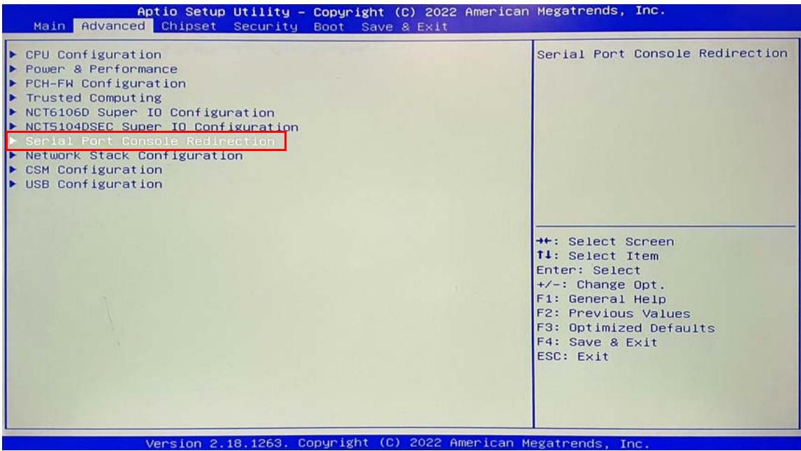
![Aptio Setup Utility - Copyright (C) 2022 American Megatrends, Inc.\nMain Advanced Chipset Security Boot Save & Exit\nCPU Configuration\nPower & Performance\nPCH-FW Configuration\nTrusted Computing\nNCT6106D Super IO Configuration\nNCT5104DSEC Super IO Configuration\nSerial Port Console Redirection\nNetwork Stack Configuration\nCSM Configuration\nUSB Configuration\nSerial Port Console Redirection\n+: Select Screen\n↑↓: Select Item\nEnter: Select\n+/-: Change Opt.\nF1: General Help\nF2: Previous Values\nF3: Optimized Defaults\nF4: Save & Exit\nESC: Exit\nVersion 2.18.1263. Copyright (C) 2022 American Megatrends, Inc.](.hperc-kbl-m-50m-00048-1020-12/51769619d981c69e19213ec62c7a48b91e94d19779f4d2b3d11b007e4480b895.jpg)

To enable console redirection for COM1, set COM1 Console Redirection to "Enabled".
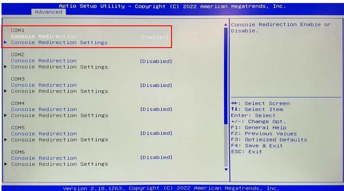
![Aptio Setup Utility - Copyright (C) 2022 American Megatrends, Inc.\nAdvanced\nCOM1\nConsole Redirection (Enabled)\nConsole Redirection Settings\nCOM2\nConsole Redirection (Disabled)\nConsole Redirection Settings\nCOM3\nConsole Redirection (Disabled)\nConsole Redirection Settings\nCOM4\nConsole Redirection (Disabled)\nConsole Redirection Settings\nCOM5\nConsole Redirection (Disabled)\nConsole Redirection Settings\nCOM6\nConsole Redirection (Disabled)\nConsole Redirection Settings\nConsole Redirection Enable or\nDisable.\n+:-: Select Screen\n↑↓: Select Item\nEnter: Select\n+/-: Change Opt.\nF1: General Help\nF2: Previous Values\nF3: Optimized Defaults\nF4: Save & Exit\nESC: Exit\nVersion 2.18.1263. Copyright (C) 2022 American Megatrends, Inc.](.hperc-kbl-m-50m-00048-1020-12/7ecba498175bccce041b05d74e3afe09ed84d97ccf30333eb196e5435c41a675.jpg)

Super I/O COM Port Legend

<table><tr><td>Super I/O</td><td>COM Port</td></tr><tr><td rowspan="3">NCT5104</td><td>COM1</td></tr><tr><td>COM2</td></tr><tr><td>COM3</td></tr><tr><td rowspan="4">NCT6106</td><td>COM4</td></tr><tr><td>COM5</td></tr><tr><td>COM6</td></tr><tr><td>COM7</td></tr></table>

Unless necessary, do not change the default console redirection settings.

<table><tr><td rowspan="2">COM1Console Redirection SettingsTerminal Type [ANSI]Bits per second [115200]Data Bits [8]Parity [None]Stop Bits [1]Flow Control [None]VT-UTF8 Combo Key Support [Enabled]Recorder Mode [Disabled]Resolution 100x31 [Disabled]Putty KeyPad [VT100]</td><td>Emulation: ANSI: ExtendedASCII char set. VT100: ASCIIchar set. VT100+: ExtendsVT100 to support color, function keys, etc. VT-UTF8: Uses UTF8 encoding to mapUnicode chars onto 1 or more bytes.</td></tr><tr><td>++: Select Screen↑↓: Select ItemEnter: Select+/-: Change Opt.F1: General HelpF2: Previous ValuesF3: Optimized DefaultsF4: Save &amp; ExitESC: Exit</td></tr></table>

Save and exit the BIOS configuration page. Reboot the system for the changes to take effect.

Open a serial console utility such as Putty (https://www.putty.org/).

▶ Set the COM port to match your hardware
▶ Ensure BAUD rate, parity, and flow control are set in sync with BIOS settings

![PuTTY Configuration\nCategory:\nSession\nLogging\nTerminal\nKeyboard\nBell\nFeatures\nWindow\nAppearance\nBehaviour\nTranslation\nSelection\nColours\nConnection\nData\nProxy\nSSH\nSerial\nTelnet\nRlogin\nSUPDUP\nBasic options for your PuTTY session\nSpecify the destination you want to connect to\nSerial line Speed\nCOM3 115200\nConnection type:\nSSH Serial Other: Telnet\nLoad, save or delete a stored session\nSaved Sessions\nHPERC\nDefault Settings\nHPERC\nLoad\nSave\nDelete\nClose window on exit:\nAlways Never Only on clean exit\nAbout Help Open Cancel](.hperc-kbl-m-50m-00048-1020-12/c1d1b229a2f9438ab82b1b23b9d189a1f91f4c3c43a53a8f4d4f18a81ca7e9b2.jpg)

![PuTTY Configuration\nCategory:\nSession\nLogging\nTerminal\nKeyboard\nBell\nFeatures\nWindow\nAppearance\nBehaviour\nTranslation\nSelection\nColours\nConnection\nData\nProxy\nSSH\nSerial\nTelnet\nRlogin\nSUPDUP\nOptions controlling local serial lines\nSelect a serial line\nSerial line to connect to COM3\nConfigure the serial line\nSpeed (baud) 115200\nData bits 8\nStop bits 1\nParity None\nFlow control None\nAbout Help Open Cancel](.hperc-kbl-m-50m-00048-1020-12/311c689fb1b52ae47cf43be860a12402861555c62feb6cf69a58d9b754126b35.jpg)

Click "Open" to establish serial console connection, then power on HPERC system. Once HPERC powers on, press "delete" and wait for the BIOS menu to appear.

COM3 - PuTTY

![Aptio Setup Utility - Copyright (C) 2022 American Megatrends, Inc.\nMain Advanced Chipset Security Boot Save & Exit\nBIOS Information\nChoose the system\nBIOS Vendor American Megatrends rdefault language\nCore Version 5.12\nCompliancy UEFI 2.6; PI 1.4\nProject Version HPERC-KBL 1.04.10\nBuild Date and Time 05/19/2022\nAccess Level Administrator\nProcessor Information\nName Kabylake Halo\nCPU Signature Intel(R) Xeon(R) CPU\nE3-1505M v6 @ 3.00GHz\nCPU Speed 3000 MHz\nProcessor ID 0x906E9\nStepping B0\nNumber of Processors 4Core(s) / 8Thread(s)\nMicrocode Revision 8E\nGT Info GT2 (1100 MHz)\n((: Select Screen\n: Select Item\nEnter: Select\n+/-: Change Opt.\nF1: General Help\nF2: Previous Values\nF3: Optimized Defaults\nF4: Save & Exit\nESC: Exit](.hperc-kbl-m-50m-00048-1020-12/a6b4585b9add60250516742d49db746c059d73212efb17f9b8117f9924b0868c.jpg)

Version 2.18.1263. Copyright (C) 2022 American Megatrends, Inc.

AB

This page intentionally left blank.

# Important Safety Instructions

For user safety, please read and follow all instructions, WARNINGS, CAUTIONS, and NOTES marked in this manual and on the associated equipment before handling/operating the equipment.

▶ Read these safety instructions carefully.
- Keep this user’s manual for future reference.
▶ Read the specifications section of this manual for detailed information on the operating environment of this equipment.
▶ When installing/mounting or uninstalling/removing equipment:

▷ Turn off power and unplug any power cords/cables.

▶ To avoid electrical shock and/or damage to equipment:

▷ Keep equipment away from water or liquid sources;
Keep equipment away from high heat or high humidity;
Keep equipment properly ventilated (do not block or cover ventilation openings);
Make sure to use recommended voltage and power source settings;
Always install and operate equipment near an easily accessible electrical socket-outlet;
▶ Secure the power cord (do not place any object on/over the power cord);
▶ Only install/attach and operate equipment on stable surfaces and/or recommended mountings; and,
If the equipment will not be used for long periods of time, turn off and unplug the equipment from its power source.

▶ Never attempt to fix the equipment. Equipment should only be serviced by qualified personnel.

▶ A Lithium-type battery may be provided for uninterrupted, backup or emergency power.

![The image shows a yellow triangular warning sign with a thick black border. Inside the triangle is a large black exclamation point. Below the triangle, the word 'CAUTION:' is printed in black capital letters.](.hperc-kbl-m-50m-00048-1020-12/0ce5174deeb7a66f462bbdacb3ac4813c9a3dc6db895d0e329adf642fde0165a.jpg)

Risk of explosion if battery is replaced with one of an incorrect type. Dispose of used batteries appropriately.

▶ Equipment must be serviced by authorized technicians when:

The power cord or plug is damaged;
▷ Liquid has penetrated the equipment;
It has been exposed to high humidity/moisture;
It is not functioning or does not function according to the user's manual;
It has been dropped and/or damaged; and/or,
It has an obvious sign of breakage.

This page intentionally left blank.

# Getting Service

Ask an Expert: http://askanexpert.adlinktech.com

# ADLINK Technology, Inc.

No. 66, Huaya 1st Road, Guishan District, Taoyuan City 333411, Taiwan

Tel: +886-3-216-5088

Fax: +886-3-328-5723

Email: service@adlinktech.com

# Ampro ADLINK Technology, Inc.

6450 Via Del Oro, San Jose, CA 95119-1208, USA

Tel: +1-408-360-0200

Toll Free:+1-800-966-5200 (USA only)

Fax: +1-408-600-1189

Email: info@adlinktech.com

# ADLINK Technology (China) Co., Ltd.

300 Fang Chun Rd., Zhangjiang Hi-Tech Park, Pudong New Area, Shanghai, 201203, China

Tel: +86-21-5132-8988

Fax: +86-21-5132-3588

Email: market@adlinktech.com

# ADLINK Technology GmbH

Hans-Thoma-Straße 11, D-68163 Mannheim, Germany

Tel: +49-621-43214-0

Fax: +49-621 43214-30

Email: germany@adlinktech.com

Please visit the Contact page at www.adlinktech.com for information on how to contact the ADLINK regional office nearest you.
[🔗 Link to the original document](.hperc-kbl-m-50m-00048-1020-12/hperc-kbl-m-50m-00048-1020-12.pdf)