# IMB-C47H

# User’s Manual

ATX Motherboard with 12th/13th/14th Gen Intel® Core™ i9/i7/i5/i3 Processors and Intel® H610 Chipset

![Close-up of a computer motherboard with visible CPU socket, RAM slots, and I/O ports (no readable text or symbols)](.imb-c47h-50m-13020-1020-12/5516a2b5d2fc37a8b7039efff24ba10a76b3646689dfc85440a339f156328758.jpg)

Manual Rev.: Rev. 1.2

Revision Date: March 14, 2025

Part Number: 50M-13020-1020

# Preface

# Copyright

Copyright 2025 ADLINK Technology, Inc. This document contains proprietary information protected by copyright. All rights are reserved. No part of this manual may be reproduced by any mechanical, electronic, or other means in any form without prior written permission of the manufacturer.

# Disclaimer

The information in this document is subject to change without prior notice in order to improve reliability, design, and function and does not represent a commitment on the part of the manufacturer. In no event will the manufacturer be liable for direct, indirect, special, incidental, or consequential damages arising out of the use or inability to use the product or documentation, even if advised of the possibility of such damages.

# Environmental Responsibility

ADLINK is committed to fulfill its social responsibility to global environmental preservation through compliance with the European Union's Restriction of Hazardous Substances (RoHS) directive and Waste Electrical and Electronic Equipment (WEEE) directive. Environmental protection is a top priority for ADLINK. We have enforced measures to ensure that our products, manufacturing processes, components, and raw materials have as little impact on the environment as possible. When products are at their end of life, our customers are encouraged to dispose of them in accordance with the product disposal and/or recovery programs prescribed by their nation or company.

![Symbol of a trash bin crossed with two crossed lines and a solid rectangle below (no text or labels)](.imb-c47h-50m-13020-1020-12/93c8c8904a525b5e9de25d9db31cceaae2f8e51b9301ce144a1c87d9e7ad3bd5.jpg)

Battery Labels (for products with battery)

![Simple line drawing of a trash bin crossed out by two diagonal lines (no text or symbols)](.imb-c47h-50m-13020-1020-12/38c91eea011ba3bb42a3e791cceaec88ae5c76ed506f72d7191e20a62ac83f22.jpg)

![The image displays a black-and-white graphic featuring the universal recycling symbol—three arrows chasing each other in a triangular formation—centered within a thick black square outline. Directly below the square, the text 'Li-ion' is written in a large, bold, black sans-serif font.](.imb-c47h-50m-13020-1020-12/955478f60d73c03c629c701a9ab26d600b6f39f5751b728204692117a1da0a7e.jpg)

![RECYCLF\nRBRC\nLi-ion\n1.800.822.8837](.imb-c47h-50m-13020-1020-12/3814d8a882f95d1be8ab2ce12c0bd6e9774915e669c1f0ba0a99802b7c10523e.jpg)

![廢電池請回收](.imb-c47h-50m-13020-1020-12/563b1d030f2250620492166f15e97b0a5a8a9d6d50b87382cf8f3fa7d19946ef.jpg)

# California Proposition 65 Warning

![The image displays a yellow equilateral triangle with a thick black border, centered on a white background. Inside the triangle is a black exclamation point.](.imb-c47h-50m-13020-1020-12/959a5accdb9e644b97cf04c8e05ef5ad3db96a8f325094c9f73c0de4446d5ae4.jpg)

WARNING: This product can expose you to chemicals including acrylamide, arsenic, benzene, cadmium, Tris(1,3-dichloro-2-propyl)phosphate (TDCPP), 1,4-Dioxane, formaldehyde, lead, DEHP, styrene, DINP, BBP, PVC, and vinyl materials, which are known to the State of California to cause cancer, and acrylamide, benzene, cadmium, lead, mercury, phthalates, toluene, DEHP, DIDP, DnHP,

DBP, BBP, PVC, and vinyl materials, which are known to the State of California to cause birth defects or other reproductive harm. For more information go to www.P65Warnings.ca.gov.

# Trademarks

Product names mentioned herein are used for identification purposes only and may be trademarks and/or registered trademarks of their respective companies.

Revision History

<table><tr><td>Revision</td><td>Description</td><td>Date</td><td>By</td></tr><tr><td>1.0</td><td>Initial release</td><td>2024-10-15</td><td>AL</td></tr><tr><td>1.1</td><td>Introduction and specifications updated</td><td>2025-01-20</td><td>AL</td></tr><tr><td>1.2</td><td>Specifications and connector pinouts updated</td><td>2025-03-14</td><td>AL</td></tr></table>

# Table of Contents

# Preface...

# List of Figures .... ..vi

# List of Tables...... ..vi

# 1 Introduction....

1.1 Packing List ..
1.2 Optional Accessories .

# 2 Specifications ....

2.1 Core System . .3
2.2 I/O Interface .. .4
2.3 Video .4
2.4 Audio .4
2.5 LAN... .5
2.6 Temperatures . ..5
2.7 Humidity... ..5
2.8 Certificate (EMC) .. .5
2.9 Form Factor .. .5
2.10 Operating Systems . .5
2.11 Functional Block Diagram 6

# 3 Mechanical Layout ..

3.1 I/O Panel Connector Locations ...
3.2 Mechanical Dimensions . .11

# 4 Connector Pinouts .. .13

4.1 Rear I/O Connectors .. .13
4.2 Onboard Headers / Connectors . .15
4.3 Jumper and Switch Settings. ..19
4.4 Expansion Slots .. ..23

# 5 Driver Installation .... .25

# 6 BIOS Settings..... .27

6.1 Menu Structure . .27
6.2 Main Menu. ..28
6.3 Advanced.. ..28
6.4 Chipset ... ..32
6.5 Security.. .34
6.6 Boot . .35

6.7 Save & Exit .. ..36

Safety Instructions.... .37

Getting Services... ..38

# List of Figures

Figure 1: Functional block diagram. .6
Figure 2: I/O panel connector locations .
Figure 3: Onboard connector – header and jumper locations.. .8
Figure 4: Mechanical dimensions . ..11
Figure 5: Mechanical dimensions – I/O panel.. .11

# List of Tables

Table 1: IMB-C47H Series.
Table 2: I/O panel connector definitions .
Table 3: Onboard connector – header and jumper definitions. 9

# 1 Introduction

ADLINK IMB-C47H ATX is an industrial motherboard supporting 12th/13th/14th Generation Intel® Core™ i9/i7/i5/i3 desktop processors, an Intel® H610 Chipset, and 7 PCIe expansion slots to provide a cost-competitive embedded computing solution. It includes high-speed data transfer interfaces such as PCIe 4.0, USB 3.0, and SATA 6 Gb/s (SATA III), and dual-channel DDR4 3200 MHz RAM for industrial automation applications. With industrial-grade I/O port design, the IMB-C47H offers a significant competitive advantage for embedded computing applications in terms of device compatibility, durable connectivity, and extreme environment readiness.

Table 1: IMB-C47H Series

<table><tr><td>Model Name</td><td>M.2 M-Key signal</td></tr><tr><td>IMB-C47H</td><td>SATA</td></tr><tr><td>IMB-C47H/NVMe</td><td>NVMe</td></tr></table>

# 1.1 Packing List

IMB-C47H ATX motherboard
• Rear I/O shield

# 1.2 Optional Accessories

CPU cooler for 65W CPU (Part Number: 32-20976-0000-A0)
• 2-port USB2.0 cable with bracket (Part Number: 30-25010-3010)
• 4-port USB 2.0 cable with bracket (Part Number 30-25009-3000)
• SATA cable with bracket (Part Number: 30-10057-7000)
• 2-port COM cable (L=450mm) with bracket (Part Number: 30-25003-3000)
• 2-port COM cable (L=600mm) with bracket (Part Number: 30-25003-5000-A0)

This page intentionally left blank.

# 2 Specifications

# 2.1 Core System

CPU:

<table><tr><td>Family</td><td>Number</td><td>CPU Core</td><td>Frequency (GHz)</td><td>Cache (MB)</td><td>Power</td></tr><tr><td>Raptor Lake-S Refresh</td><td>i9-14900T</td><td>24</td><td>1.1GHz</td><td>36MB</td><td>35</td></tr><tr><td>Raptor Lake-S Refresh</td><td>i9-14900</td><td>24</td><td>2.0GHz</td><td>36MB</td><td>65</td></tr><tr><td>Raptor Lake-S Refresh</td><td>i7-14700T</td><td>20</td><td>1.3GHz</td><td>33MB</td><td>35</td></tr><tr><td>Raptor Lake-S Refresh</td><td>i7-14700</td><td>20</td><td>2.1GHz</td><td>33MB</td><td>65</td></tr><tr><td>Raptor Lake-S Refresh</td><td>i5-14500T</td><td>14</td><td>1.7GHz</td><td>24MB</td><td>35</td></tr><tr><td>Raptor Lake-S Refresh</td><td>i5-14500</td><td>14</td><td>2.6GHz</td><td>24MB</td><td>65</td></tr><tr><td>Raptor Lake-S Refresh</td><td>i3-14100T</td><td>4</td><td>2.7GHz</td><td>12MB</td><td>35</td></tr><tr><td>Raptor Lake-S Refresh</td><td>i3-14100</td><td>4</td><td>3.5GHz</td><td>12MB</td><td>60</td></tr><tr><td>Raptor Lake-S</td><td>i9-13900E</td><td>24</td><td>1.8GHz</td><td>36MB</td><td>65</td></tr><tr><td>Raptor Lake-S</td><td>i7-13700TE</td><td>16</td><td>1.1GHz</td><td>30MB</td><td>35</td></tr><tr><td>Raptor Lake-S</td><td>i7-13700T</td><td>16</td><td>1.4GHz</td><td>30MB</td><td>35</td></tr><tr><td>Raptor Lake-S</td><td>i7-13700</td><td>16</td><td>2.1GHz</td><td>30MB</td><td>65</td></tr><tr><td>Raptor Lake-S</td><td>i5-13600</td><td>14</td><td>2.0GHz</td><td>24MB</td><td>65</td></tr><tr><td>Raptor Lake-S</td><td>i5-13500T</td><td>14</td><td>1.6GHz</td><td>24MB</td><td>35</td></tr><tr><td>Raptor Lake-S</td><td>i5-13400</td><td>10</td><td>1.8GHz</td><td>20MB</td><td>65</td></tr><tr><td>Raptor Lake-S</td><td>i3-13100T</td><td>4</td><td>2.5GHz</td><td>12MB</td><td>35</td></tr><tr><td>Raptor Lake-S</td><td>i3-13100E</td><td>4</td><td>3.3GHz</td><td>12MB</td><td>60</td></tr><tr><td>Alder Lake-S</td><td>i9-12900E</td><td>16</td><td>2.3GHz</td><td>30MB</td><td>65</td></tr><tr><td>Alder Lake-S</td><td>i7-12700TE</td><td>12</td><td>1.4GHz</td><td>25MB</td><td>35</td></tr><tr><td>Alder Lake-S</td><td>i7-12700</td><td>12</td><td>1.6GHz</td><td>25MB</td><td>65</td></tr><tr><td>Alder Lake-S</td><td>i5-12500E</td><td>6</td><td>2.9GHz</td><td>18MB</td><td>65</td></tr><tr><td>Alder Lake-S</td><td>i5-12400</td><td>6</td><td>2.5GHz</td><td>18MB</td><td>65</td></tr><tr><td>Alder Lake-S</td><td>i3-12100</td><td>4</td><td>3.3GHz</td><td>12MB</td><td>60</td></tr><tr><td>Alder Lake-S</td><td>i3-12100TE</td><td>4</td><td>2.1GHz</td><td>12MB</td><td>35</td></tr><tr><td>Alder Lake-S</td><td>G7400TE</td><td>2</td><td>3.0GHz</td><td>6MB</td><td>35</td></tr></table>

+3.3V voltage
+5V voltage
+12V voltage
CPU temperature
• System temperature

Chipset: Intel® H610 Express Chipset

Memory: 2x 288-pin dual-channel DDR4 3200 MHz, up to 64 GB

BIOS: AMI® UEFI BIOS, 256 Mb SPI Flash Memory

Hardware Monitor: CPU voltage

CPU fan speed
• System fan speed

# 2.2 I/O Interface

# Expansion slots:

1x PCIe Gen4 x16
• 3x PCIe x4 (Support PCIe Gen3 x2 signal, slot3 co-lay with M.2 M-key 2242/2280, BOM selection)

o IMB-C47H: 3x PCIe x4 slot

o IMB-C47H/NVMe: 2x PCIe x4 slot

3x PCI

• SATA: 4x SATA 6.0 Gb/s connectors, SATA1 co-lay with M.2 M-key 2242/2280, BOM selection

IMB-C47H: 3x SATA3.0 connectors
IMB-C47H/NVMe: 4x SATA3.0 connectors

# USB:

4x USB 3.0 connector (rear)
• 2x USB 2.0 connector (rear)
• 4x USB 2.0 (via pin headers, 1x co-lay with vertical Type A)

# COM:

• 4x RS-232 (COM1 by DB9/M, others via headers)
• 2x RS-232/485 (via headers)

• PS/2 Combo Port: 1x PS/2 keyboard/mouse pin header
DIO: 8-bit GPIO
TPM: Support Intel PTT
M.2 connectors:

• 1x M.2 M-key 2242/2280 (supports SATA/NVMe SSD, BOM selection)

o IMB-C47H: SATA SSD
IMB-C47H/NVMe: NVMe SSD

# 2.3 Video

Supports four independent displays:

• 1x DVI-D (DVI-I), max resolution up to 1920x1200@60Hz
1x HDMI 1.4b, max resolution up to 4096x2160@30Hz
1x VGA, max resolution up to 1920x1200@60Hz

# 2.4 Audio

• Audio Codec: Realtek® ALC897
• Interfaces: 1x Mic-in, 1x Line-in, and 1x Line-out connectors (rear)

# 2.5 LAN

• LAN1: Intel® I219-V via RJ45 connector, with 10/100/1000 Mbps
• LAN2: Intel® I226-V via RJ45 connector, with 10/100/1000 Mbps

# 2.6 Temperatures

Operating Temperature: $0 ^ { \circ } \mathsf { C }$ to $6 0 ^ { \circ } \mathsf { C }$
Storage Temperature: $\angle 0 ^ { \circ } \mathsf { C }$ to $7 5 ^ { \circ } \mathsf { C }$

# 2.7 Humidity

$6 0 ^ { \circ } \mathsf { C }$ at 95% RH, non-condensing

# 2.8 Certificate (EMC)

CE/FCC Class A

# 2.9 Form Factor

• ATX: 305 mm x 244 mm (W x L)

# 2.10 Operating Systems

Microsoft® Windows® 10, 64-bit
Microsoft® Windows® 11, 64-bit

# 2.11 Functional Block Diagram

![Based on the provided flowchart, here is the accurate description of the labeled blocks and their connections:\n\n**Central Components**\n*   **12/13/14th Gen Intel Processor** (Top Red Block)\n*   **Intel PCH H610** (Large Red Vertical Block)\n\n**Connections from 12/13/14th Gen Intel Processor**\n*   Connects to **VGA DB9FM Port** via **Converter** (Label: **DDI**)\n*   Connects to **HDMI TYPE-A** (Label: **DDI**)\n*   Connects to **DVI-D Port** (Label: **DDI**)\n*   Connects to **DIMM0+DIMM1** leading to **DDR4 2x U-DIMM**\n*   Connects to **PEG 16X(0-15)** leading to **PCIE x16 Slot**\n*   Connects to **Intel PCH H610** (Label: **DMI**)\n\n**Connections from Intel PCH H610 (Left Side)**\n*   Connects to **AUDIO CODEC** (Label: **HDA**)\n    *   **AUDIO CODEC** connects to **SPDIF Header**\n    *   **AUDIO CODEC** connects to **L-OUT/IN/MIC Phone Jack**\n    *   **AUDIO CODEC** connects to **L-OUT+MIC Header**\n*   Connects to **I219-V** (Label: **GbE**) which connects to **RJ45 Port**\n*   Connects to **I226-V** (Label: **PCIE**) which connects to **RJ45 Port**\n*   Connects to **3x SATA Port** (Label: **3x SATA**)\n*   Connects to **SATA Port** (Label: **SATA**)\n    *   (Dashed line connects **SATA Port** to **M.2 M-Key 2242/2280**)\n*   Connects to **M.2 M-Key 2242/2280** (Label: **PCIE 2X**)\n*   Connects to **PCIE x4 Port3** (Label: **PCIE 2X**)\n*   Connects to **PCIE x4 Port2** (Label: **PCIE 4X**)\n*   Connects to **PCIE x4 Port1** (Label: **PCIE 2X**)\n*   Connects to **USB3.0 2xTYPE-A** (Label: **2x USB3.0 + 2x USB2.0**)\n*   Connects to **USB3.0 2xTYPE-A** (Label: **2x USB3.0 + 2x USB2.0**)\n*   Connects to **PCI Bridge** (Label: **PCIE**) which connects to **3x PCI Port**\n*   Connects to **SMBus Header** (Label: **SMBus**)\n\n**Connections from Intel PCH H610 (Right Side)**\n*   Connects to **USB2.0 Vertical-TYPE-A** (Label: **1x USB2.0**)\n*   Connects to **USB2.0 2xDual-Header** (Label: **4x USB2.0**)\n*   Connects to **USB2.0 2xDual-Header** (Label: **3x USB2.0**)\n*   Connects to **2x USB2.0 TYPE-A (+PS2)** (Label: **2x USB2.0**)\n    *   (Note: Text **KB+MS** appears below this block)\n*   Connects to **Super I/O** (Label: **eSPI**)\n    *   **Super I/O** connects to **COM1 DB9M** (Label: **RS232**)\n    *   **Super I/O** connects to **COM2 Header** (Label: **RS232**)\n    *   **Super I/O** connects to **COM3 Header** (Label: **RS232/485**)\n    *   **Super I/O** connects to **COM4 Header** (Label: **RS232/485**)\n    *   **Super I/O** connects to **COM5/6 Header** (Label: **RS232**)\n    *   **Super I/O** connects to **3x FAN Header** (Label: **FAN1~3**)\n    *   **Super I/O** connects to **GPIO Header** (Label: **GPIOx8**)\n    *   **Super I/O** connects to **CASE OPEN Header**\n*   Connects to **Header** (Label: **eSPI**)\n*   Connects to **F-PANEL** (Label: **PWR-ON,RESET,HDD LED**)](.imb-c47h-50m-13020-1020-12/c8ebec632e898ee84b247327f262a319989d810aa269005535bfdf01b6e46f9a.jpg)

Figure 1: Functional block diagram

# 3 Mechanical Layout

# 3.1 I/O Panel Connector Locations

![A\nB\nC\nD-2\nD-1\nI-1\nE-2\nE-1\nF\nG\nH-4\nH-3\nH-2\nH-1\nI-3\nI-2](.imb-c47h-50m-13020-1020-12/830561d934cbc015f2b53f82d0309993723579353271b04c59abdee23f4fe2e8.jpg)

Figure 2: I/O panel connector locations

Table 2: I/O panel connector definitions

<table><tr><td>Item</td><td>Description</td><td>Description</td></tr><tr><td>A</td><td>PS/2_USB1 (PS/2)</td><td>PS/2 Connector (Keyboard &amp; Mouse)</td></tr><tr><td>B</td><td>DVI_VGA1 (VGA)</td><td>VGA DB15 Connector</td></tr><tr><td>C</td><td>COM1</td><td>COM1 Connector</td></tr><tr><td>D-1</td><td>RJ45_USB1 (LAN1)</td><td>GBE LAN RJ45 Connector1</td></tr><tr><td>D-2</td><td>RJ45_USB2 (LAN2)</td><td>GBE LAN RJ45 Connector2</td></tr><tr><td>E-1</td><td>PS/2_USB1 (USB1)</td><td>USB2.0 TYPE-A Connector</td></tr><tr><td>E-2</td><td>PS/2_USB1 (USB2)</td><td>USB2.0 TYPE-A Connector</td></tr><tr><td>F</td><td>DVI_VGA1 (DVI-D)</td><td>DVI-I 24+4P/F Connector (Support DVI-D)</td></tr><tr><td>G</td><td>HDMI1</td><td>HDMI TYPE-A Connector</td></tr><tr><td>H-1</td><td>RJ45_USB1 (USB1)</td><td>USB3.0 TYPE-A Connector1</td></tr><tr><td>H-2</td><td>RJ45_USB1 (USB2)</td><td>USB3.0 TYPE-A Connector2</td></tr><tr><td>H-3</td><td>RJ45_USB2 (USB3)</td><td>USB3.0 TYPE-A Connector3</td></tr><tr><td>H-4</td><td>RJ45_USB2 (USB4)</td><td>USB3.0 TYPE-A Connector4</td></tr><tr><td>I-1</td><td>AUDIO1 (BLUE)</td><td>Line-In 3.5mm Jack</td></tr><tr><td>I-2</td><td>AUDIO1 (GREEN)</td><td>Line-Out 3.5mm Jack</td></tr><tr><td>I-3</td><td>AUDIO1 (PINK)</td><td>MIC-In 3.5mm Jack</td></tr></table>

![ADLINK\nIMB-C47H\n1\n2\n3\n4\n5-3\n5-4\n5-1\n5-2\n6\n7\n8\n9\n10\n11\n12\n13\n42\n43\n44\n45-\n45-\n41\n40\n39\n38\n37\n36\n35\n34\n33\n32\n31 30 29 28 27 26 25-1 25-2 25-3 25-4 25-5](.imb-c47h-50m-13020-1020-12/4759e8f0c9d6ca26e9536c3f743f6c28a4a2895109676821f1c993441ae0e02a.jpg)

Figure 3: Onboard connector – header and jumper locations

Table 3: Onboard connector – header and jumper definitions

<table><tr><td>Item</td><td>Description</td><td>Description</td></tr><tr><td>1</td><td>VOLT1</td><td>Power Monitor Wafer</td></tr><tr><td>2</td><td>PSON1</td><td>Power On Wafer</td></tr><tr><td>3</td><td>ATX1</td><td>ATX 24P Power Input Connector</td></tr><tr><td>4</td><td>USB2_1</td><td>USB2.0 Internal Vertical TYPE-A Connector</td></tr><tr><td>5-1</td><td>SATA1</td><td>SATA3.0 Connector1, IMB-C47H/NVMe only</td></tr><tr><td>5-2</td><td>SATA2</td><td>SATA3.0 Connector2</td></tr><tr><td>5-3</td><td>SATA3</td><td>SATA3.0 Connector3</td></tr><tr><td>5-4</td><td>SATA4</td><td>SATA3.0 Connector4</td></tr><tr><td>6</td><td>CLR_CMOS1</td><td>CMOS Clear Select Jumper</td></tr><tr><td>7</td><td>J_ESPI1</td><td>ESPI Header</td></tr><tr><td>8</td><td>J_COPEN1</td><td>Case Open Header</td></tr><tr><td>9</td><td>J_DNX1</td><td>DNX Force Reload Disable/Enable Select Jumper</td></tr><tr><td>10</td><td>SMBUS1</td><td>SMBus Wafer</td></tr><tr><td>11</td><td>M.2_SSD_M1</td><td>M.2 M-Key 2242/2280 (Supports SATA/NVMe SSD, BOM selection)IMB-C47H: SATA SSDIMB-C47/NVMe: NVMe SSD</td></tr><tr><td>12</td><td>J_AT/ATX1</td><td>AT or ATX Select Jumper</td></tr><tr><td>13</td><td>JP19</td><td>Watch Dog Reset Enable/Disable Select Jumper</td></tr><tr><td>14</td><td>JP12</td><td>COM4 RS485 Signal 120Ω Resistive Termination Select Jumper</td></tr><tr><td>15</td><td>JP10</td><td>COM4 RS232/RS485 Select Jumper1</td></tr><tr><td>16</td><td>JP9</td><td>COM3 RS485 Signal 120Ω Resistive Termination Select Jumper</td></tr><tr><td>17</td><td>JP7</td><td>COM3 RS232/RS485 Select Jumper1</td></tr><tr><td>18</td><td>JP6</td><td>COM6 DCD/5V+ RI/12V Select Jumper</td></tr><tr><td>19</td><td>JP5</td><td>COM5 DCD/5V+ RI/12V Select Jumper</td></tr><tr><td>20</td><td>JP11</td><td>COM4 RS232/RS485 Select Jumper2</td></tr><tr><td>21</td><td>JP4</td><td>COM4 DCD/5V+ RI/12V Select Jumper</td></tr><tr><td>22</td><td>JP8</td><td>COM3 RS232/RS485 Select Jumper2</td></tr><tr><td>23</td><td>JP3</td><td>COM3 DCD/5V+ RI/12V Select Jumper</td></tr><tr><td>24</td><td>JP2</td><td>COM2 DCD/5V+ RI/12V Select Jumper</td></tr><tr><td>25-1</td><td>COM2</td><td>COM2 Headers</td></tr><tr><td>25-2</td><td>COM3</td><td>COM3 Headers</td></tr><tr><td>25-3</td><td>COM4</td><td>COM4 Headers</td></tr><tr><td>25-4</td><td>COM5</td><td>COM5 Headers</td></tr><tr><td>25-5</td><td>COM6</td><td>COM6 Headers</td></tr><tr><td>26</td><td>F_PANEL1</td><td>Front Panel Header</td></tr><tr><td>27</td><td>F_USB2_1</td><td>Front Dual-USB2.0 Header</td></tr><tr><td>28</td><td>F_USB2_2</td><td>Front Dual-USB2.0 Header</td></tr><tr><td>29</td><td>J_GPIO1</td><td>GPIO Header</td></tr><tr><td>30</td><td>SYS_FAN2</td><td>System FAN2 Wafer</td></tr><tr><td>31</td><td>SYS_FAN1</td><td>System FAN1 Wafer</td></tr><tr><td>32</td><td>PCI2</td><td>PCI Slot2</td></tr><tr><td>33</td><td>PCI1</td><td>PCI Slot1</td></tr><tr><td>34</td><td>PCIE_4X_SLOT3</td><td>PCIE4X Slot3, IMB-C47H only</td></tr><tr><td>35</td><td>JP14</td><td>PCI CLK 66MHz Disable/ Enable Select Jumper</td></tr><tr><td>36</td><td>PCIE_4X_SLOT2</td><td>PCIE4X Slot2</td></tr><tr><td>37</td><td>J_SPDIF1</td><td>SPDIF Out Header</td></tr><tr><td>38</td><td>PCIE_4X_SLOT1</td><td>PCIE4X Slot1</td></tr><tr><td>39</td><td>PCI3</td><td>PCI Slot3</td></tr><tr><td>40</td><td>PCIE_16X_SLOT1</td><td>PCI-E 16x Slot</td></tr><tr><td>41</td><td>F_AUDIO1</td><td>Front Audio Header</td></tr><tr><td>42</td><td>JP1</td><td>COM1 DCD/5V+ RI/12V Select Jumper</td></tr><tr><td>43</td><td>ATX2</td><td>ATX 8P CPU Power Input Connector</td></tr><tr><td>44</td><td>CPU_FAN1</td><td>CPU Fan Wafer</td></tr><tr><td>45-1</td><td>DIMM1</td><td>DDR4 CHA DIMM Slot</td></tr><tr><td>45-2</td><td>DIMM2</td><td>DDR4 CHB DIMM Slot</td></tr></table>

# 3.2 Mechanical Dimensions

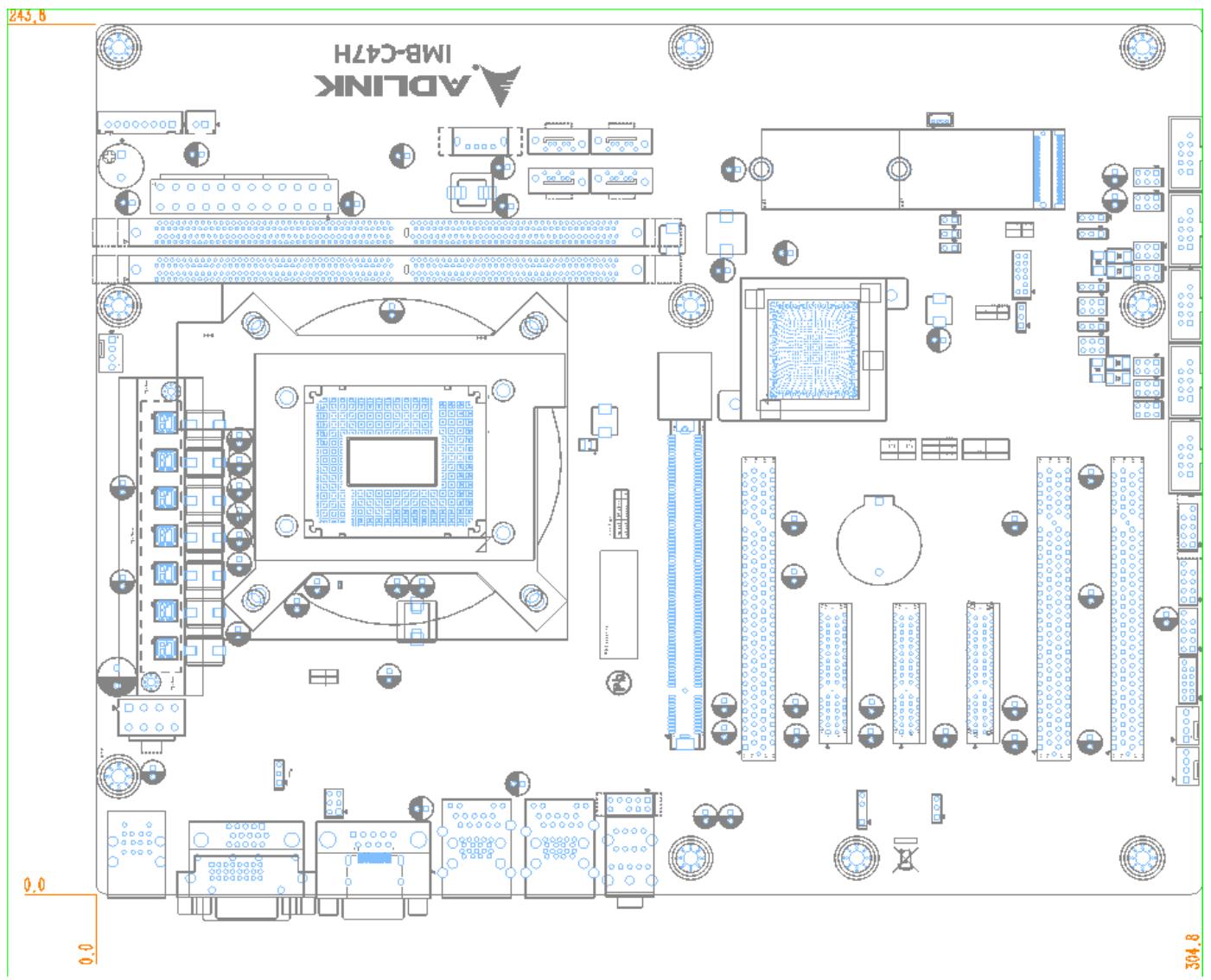
Top View
![243,8\nADBLINK\nIMB-C47H\n0.0\n0.0\n304.8](.imb-c47h-50m-13020-1020-12/67e23e70148735985d9b14ba176fdc1df794d785c0356c5d78218b98f457653c.jpg)

Dimensions: mm

Figure 4: Mechanical dimensions
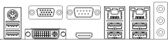
Side View
![Diagram of various electronic connectors and ports (no text or labels)](.imb-c47h-50m-13020-1020-12/a03448d4e6eae004c22e3a541ea8c8d49d0653deaee8121159cbc075572f4f21.jpg)

Dimensions: mm

Figure 5: Mechanical dimensions – I/O panel

This page intentionally left blank.

# 4 Connector Pinouts

See 3.1 Connector Locations on page 7.

# 4.1 Rear I/O Connectors

# 4.1.1 HDMI

<table><tr><td>Pin</td><td>Signal</td><td>Pin</td><td>Signal</td></tr><tr><td>1</td><td>HDMI1_CON_DP2</td><td>2</td><td>GND</td></tr><tr><td>3</td><td>HDMI1_CON_DN2</td><td>4</td><td>HDMI1_CON_DP1</td></tr><tr><td>5</td><td>GND</td><td>6</td><td>HDMI1_CON_DN1</td></tr><tr><td>7</td><td>HDMI1_CON_DP0</td><td>8</td><td>GND</td></tr><tr><td>9</td><td>HDMI1_CON_DN0</td><td>10</td><td>HDMI1_CON_CKP</td></tr><tr><td>11</td><td>GND</td><td>12</td><td>HDMI1_CON_CKN</td></tr><tr><td>13</td><td>NC</td><td>14</td><td>NC</td></tr><tr><td>15</td><td>HDMI1_DDC_CLK</td><td>16</td><td>HDMI1_DDC_DATA</td></tr><tr><td>17</td><td>GND</td><td>18</td><td>+5V_HDMI</td></tr><tr><td>19</td><td>HDMI1_CON_HPD</td><td></td><td></td></tr></table>

![The image displays a diagram of a rectangular connector with two rows of pins. Numbers label specific pin positions around the perimeter.\n\n*   **Top Left:** The numbers '19' and '17' are positioned above the left side of the upper row of pins.\n*   **Top Right:** The numbers '3' and '1' are positioned above the right side of the upper row of pins.\n*   **Bottom Left:** The number '18' is positioned below the left side of the lower row of pins.\n*   **Bottom Right:** The numbers '4' and '2' are positioned below the right side of the lower row of pins.](.imb-c47h-50m-13020-1020-12/dce87333d277301c2be20c2ec22ec1981023dacd4bc9d45d3c24e5057d654088.jpg)

# 4.1.2 VGA Connector

<table><tr><td>Pin</td><td>Signal</td><td>Pin</td><td>Signal</td></tr><tr><td>1</td><td>VGA_CON_RED</td><td>2</td><td>VGA_CON_GREEN</td></tr><tr><td>3</td><td>VGA_CON_BLUE</td><td>4</td><td>NC</td></tr><tr><td>5</td><td>GND</td><td>6</td><td>GND</td></tr><tr><td>7</td><td>GND</td><td>8</td><td>GND</td></tr><tr><td>9</td><td>+5V_HDMI</td><td>10</td><td>GND</td></tr><tr><td>11</td><td>NC</td><td>12</td><td>VGA_DDCDAT</td></tr><tr><td>13</td><td>VGA_CON_HS</td><td>14</td><td>VGA_CON_VS</td></tr><tr><td>15</td><td>VGA_DDCCLK</td><td></td><td></td></tr></table>

![The image is a line drawing of a D-sub connector. It features two hexagonal screw heads on the far left and right sides. In the center is a rectangular connector housing containing two rows of circular pins. There are 10 pins in the upper row and 10 pins in the lower row. The number '5' appears above the left side of the connector, and the number '1' appears above the right side. Below the connector, the number '15' is on the left and the number '11' is on the right.](.imb-c47h-50m-13020-1020-12/10cf28a9199eea4ae5074bd93988275efa4af7535fc910a09210c78bc3976e9b.jpg)

# 4.1.3 COM 1 (COM1 DB9/M Connector)

<table><tr><td rowspan="2">Pin</td><td>Signal</td></tr><tr><td>RS-232</td></tr><tr><td>1</td><td>PIN 1 [1]</td></tr><tr><td>2</td><td>RxD</td></tr><tr><td>3</td><td>TxD</td></tr><tr><td>4</td><td>DTR#</td></tr><tr><td>5</td><td>GND</td></tr><tr><td>6</td><td>DSR#</td></tr><tr><td>7</td><td>RTS#</td></tr><tr><td>8</td><td>CTS#</td></tr><tr><td>9</td><td>PIN 9 [1]</td></tr></table>

![1\n5\n6\n9](.imb-c47h-50m-13020-1020-12/365882658e594ccb256cc97f2bf3bb44ef43b3ba84bcf9fd0df6c56499846320.jpg)

Note: PIN1 of COM1 can be DCD (default) /5V and Pin9 of COM1 can be RI(Default) / 12V, selectable by “COM1 DCD/RI Select Jumper”. (JP3)

# 4.1.4 Ethernet Connectors (LAN1, LAN2)

RJ45\_USB1 (LAN1) (GBE LAN RJ45 Connector1)

<table><tr><td>Pin</td><td colspan="2">Signal</td><td>Pin</td><td colspan="2">Signal</td></tr><tr><td>1</td><td colspan="2">MDI1_0+</td><td>5</td><td colspan="2">MDI1_2+</td></tr><tr><td>2</td><td colspan="2">MDI1_0-</td><td>6</td><td colspan="2">MDI1_2-</td></tr><tr><td>3</td><td colspan="2">MDI1_1+</td><td>7</td><td colspan="2">MDI1_3+</td></tr><tr><td>4</td><td colspan="2">MDI1_1-</td><td>8</td><td colspan="2">MDI1_3-</td></tr><tr><td rowspan="3">LED1</td><td rowspan="3">Active LED</td><td>ACT: Blinking Green</td><td rowspan="3">LED2</td><td rowspan="3">Speed LED</td><td>1000M: Turn Orange</td></tr><tr><td>LINK only: Lights On</td><td>100M: Turn Green</td></tr><tr><td>Stop: Lights Off</td><td>10M: Lights Off</td></tr></table>

![The image displays a schematic diagram of an RJ45 connector. At the top, the text 'LED1' is on the left and 'LED2' is on the right. The central graphic shows the connector housing with two small rectangular outlines at the top and a grey filled area in the center. Below the housing, the number '8' is on the left and '1' is on the right, with thin black lines connecting the bottom of the connector to each number.](.imb-c47h-50m-13020-1020-12/8f3159fbd7bfce7cdb2d74c39d7eac32f52d0f8224f350bb65c93ef0354cdac7.jpg)

Note: RJ45\_USB1 (LAN1) I219-V does not support Intel AMT 12.0 and Intel vPro by default.

RJ45\_ USB2 (LAN2) (GBE LAN RJ45 Connector2)

<table><tr><td>Pin</td><td colspan="2">Signal</td><td>Pin</td><td colspan="2">Signal</td></tr><tr><td>1</td><td colspan="2">MDI2_0+</td><td>5</td><td colspan="2">MDI2_2+</td></tr><tr><td>2</td><td colspan="2">MDI2_0-</td><td>6</td><td colspan="2">MDI2_2-</td></tr><tr><td>3</td><td colspan="2">MDI2_1+</td><td>7</td><td colspan="2">MDI2_3+</td></tr><tr><td>4</td><td colspan="2">MDI2_1-</td><td>8</td><td colspan="2">MDI2_3-</td></tr><tr><td rowspan="3">LED1</td><td rowspan="3">Active LED</td><td>ACT: Blinking Green</td><td rowspan="3">LED2</td><td rowspan="3">Speed LED</td><td>1000M/2.5G: Turn Orange</td></tr><tr><td>LINK only: Lights On</td><td>100M: Turn Green</td></tr><tr><td>Stop: Lights Off</td><td>10M: Lights Off</td></tr></table>

# 4.2 Onboard Headers / Connectors

# 4.2.1 ATX12V Power Connector (ATX2)

This motherboard provides an 8-pin ATX 12V power connector.

<table><tr><td>Pin</td><td>Signal</td><td>Pin</td><td>Signal</td><td>Pin</td><td>Signal</td><td>Pin</td><td>Signal</td></tr><tr><td>8</td><td>ATX12V</td><td>7</td><td>ATX12V</td><td>6</td><td>ATX12V</td><td>5</td><td>ATX12V</td></tr><tr><td>4</td><td>GND</td><td>3</td><td>GND</td><td>2</td><td>GND</td><td>1</td><td>GND</td></tr></table>

![The image displays a rectangular grid divided into two rows and four columns, creating eight individual square sections. The grid is framed by double lines. Surrounding the grid are four numbers positioned at the corners: the number 8 is at the top left, the number 5 is at the top right, the number 4 is at the bottom left, and the number 1 is at the bottom right.](.imb-c47h-50m-13020-1020-12/7478be7d90a16efb7d9c5ec5817ce2ce38e1b8fb22412acfa88d97a857611891.jpg)

# 4.2.2 Fan Connectors (SYS\_FAN1/2, CPU\_FAN1)

![GND\n+12V\nFAN_SPEED_DETECTION\nFAN_SPEED_CONTROL\n1](.imb-c47h-50m-13020-1020-12/ed66bbe01a46dbdefa447e8f30781dcdc35ec8efd831ba71236abe705d19e6fe.jpg)

FAN Wafer 4\*1 Pin 2.54mm

# 4.2.3 USB Connectors (USB2\_1)

There are one USB 2.0 Type-A vertical connectors on this motherboard.

<table><tr><td>Pin</td><td>Signal</td></tr><tr><td>4</td><td>GND</td></tr><tr><td>3</td><td>USB_D+</td></tr><tr><td>2</td><td>USB_D-</td></tr><tr><td>1</td><td>USB_PWR</td></tr></table>

![A white rounded rectangle containing a vertical black bar is positioned on the left side. To the right of the rectangle, the number 4 is placed above the number 1.](.imb-c47h-50m-13020-1020-12/cad14b32b77ff0068c38bd3dd990c40e4d5949d1d6eb44e916f1106530d7670e.jpg)

# 4.2.4 SMBUS1

<table><tr><td>Pin</td><td>Signal</td></tr><tr><td>1</td><td>GND</td></tr><tr><td>2</td><td>SMB_DATA</td></tr><tr><td>3</td><td>SMB_CLK</td></tr><tr><td>4</td><td>VCC5</td></tr></table>

![A black and white image showing a vertical rectangular device, resembling a thermostat or control panel, with four small square buttons arranged vertically down its center. The number 1 is positioned in the top right corner, and the number 4 is located at the bottom right.](.imb-c47h-50m-13020-1020-12/5cda9d8cf02aa8cb9970d8b87a6b1aab899e12877eb0472b8981dc85d2e0904c.jpg)
Wafer 4\*1 Pin 1.25mm

# 4.2.5 24-pin ATX Power Input Connector (ATX1)

<table><tr><td>Pin</td><td>Signal</td><td>Pin</td><td>Signal</td></tr><tr><td>12</td><td>+3V</td><td>24</td><td>GND</td></tr><tr><td>11</td><td>+12V</td><td>23</td><td>+5V</td></tr><tr><td>10</td><td>+12V</td><td>22</td><td>+5V</td></tr><tr><td>9</td><td>ATX+5VSB</td><td>21</td><td>+5V</td></tr><tr><td>8</td><td>PWROK_PS</td><td>20</td><td>NA</td></tr><tr><td>7</td><td>GND</td><td>19</td><td>GND</td></tr><tr><td>6</td><td>+5V</td><td>18</td><td>GND</td></tr><tr><td>5</td><td>GND</td><td>17</td><td>GND</td></tr><tr><td>4</td><td>+5V</td><td>16</td><td>PSON#</td></tr><tr><td>3</td><td>GND</td><td>15</td><td>GND</td></tr><tr><td>2</td><td>+3V</td><td>14</td><td>-12V</td></tr><tr><td>1</td><td>+3V</td><td>13</td><td>+3V</td></tr></table>

![12\n24\n1\n13](.imb-c47h-50m-13020-1020-12/3a57a8e390cc7f85723683a6a5f1fd46668bcfc0eb68556c41d3f8c68d882226.jpg)

# 4.2.6 SATA Connector (SATA 1/2/3/4)

<table><tr><td>Pin</td><td>Signal</td><td>Pin</td><td>Signal</td></tr><tr><td>1</td><td>GND</td><td>5</td><td>SATA-B-</td></tr><tr><td>2</td><td>SATA-A+</td><td>6</td><td>SATA-B+</td></tr><tr><td>3</td><td>SATA-A-</td><td>7</td><td>GND</td></tr><tr><td>4</td><td>GND</td><td></td><td></td></tr></table>

![The image displays a schematic line drawing of a vertical rectangular component, likely a connector or housing. Inside a larger outer casing, there is a smaller internal structure featuring a central vertical column composed of alternating black and white rectangular blocks. A small protrusion extends from the left side of this inner structure. To the right of the outer casing, the numbers '1' and '7' appear vertically, labeling the upper and lower sections respectively.](.imb-c47h-50m-13020-1020-12/b81f9ff4f8ef561de7826239cb6ac0a3226aa2be405dd0b1ce96ce03127ca1b1.jpg)

# 4.2.7 Front Panel Header (F\_PANEL1)

This header accommodates several system front panel functions.

<table><tr><td>Pin</td><td>Signal</td><td>Pin</td><td>Signal</td></tr><tr><td>1</td><td>HDD 3.3V LED+</td><td>2</td><td>POWER 3.3V LED+</td></tr><tr><td>3</td><td>HDD 3.3V LED-</td><td>4</td><td>POWER 3.3V LED-</td></tr><tr><td>5</td><td>RESET-</td><td>6</td><td>POWER+</td></tr><tr><td>7</td><td>RESET+</td><td>8</td><td>POWER-</td></tr></table>

![The image displays a vertical stack of six rounded rectangles. The topmost rectangle is flanked by the number '1' on the left and '2' on the right, containing two small dark squares. Directly below are four rectangles, each containing two small dark squares. The bottom-most rectangle is an empty outline.](.imb-c47h-50m-13020-1020-12/0db2be848721263ea47b2014079f3c9afaab5d78e750c3c9bb23b34cf635f59a.jpg)

<table><tr><td>Pin</td><td>Signal</td><td>Pin</td><td>Signal</td></tr><tr><td>9</td><td>N/C</td><td></td><td></td></tr></table>

Front Panel Header 5\*2 Pin 2.54mm

4.2.8 COM Port Header (COM 2-6)

<table><tr><td></td><td>Pin</td><td>Signal</td><td>Pin</td><td>Signal</td></tr><tr><td rowspan="5">COM2</td><td>1</td><td>COM2_PIN1 [1]</td><td>2</td><td>COM2_DSR</td></tr><tr><td>3</td><td>COM2_RXD</td><td>4</td><td>COM2_RTS</td></tr><tr><td>5</td><td>COM2_TXD</td><td>6</td><td>COM2_CTS</td></tr><tr><td>7</td><td>COM2_DTR</td><td>8</td><td>COM2_PIN8 [1]</td></tr><tr><td>9</td><td>GND</td><td></td><td></td></tr><tr><td></td><td>Pin</td><td>Signal</td><td>Pin</td><td>Signal</td></tr><tr><td rowspan="5">COM3</td><td>1</td><td>COM3_PIN1 [2] [3]</td><td>2</td><td>COM3_DSR</td></tr><tr><td>3</td><td>COM3_PIN3 [3]</td><td>4</td><td>COM3_RTS</td></tr><tr><td>5</td><td>COM3_PIN5 [3]</td><td>6</td><td>COM3_CTS</td></tr><tr><td>7</td><td>COM3_PIN7 [3]</td><td>8</td><td>COM3_PIN8 [2] [3]</td></tr><tr><td>9</td><td>GND</td><td></td><td></td></tr><tr><td></td><td>Pin</td><td>Signal</td><td>Pin</td><td>Signal</td></tr><tr><td rowspan="5">COM4</td><td>1</td><td>COM4_PIN1 [4] [5]</td><td>2</td><td>COM4_DSR</td></tr><tr><td>3</td><td>COM4_PIN3 [4]</td><td>4</td><td>COM4_RTS</td></tr><tr><td>5</td><td>COM4_TXD</td><td>6</td><td>COM4_CTS</td></tr><tr><td>7</td><td>COM4_DTR</td><td>8</td><td>COM4_PIN8 [5]</td></tr><tr><td>9</td><td>GND</td><td></td><td></td></tr><tr><td></td><td>Pin</td><td>Signal</td><td>Pin</td><td>Signal</td></tr><tr><td rowspan="5">COM5</td><td>1</td><td>COM5_PIN1 [6]</td><td>2</td><td>COM5_DSR</td></tr><tr><td>3</td><td>COM5_RXD</td><td>4</td><td>COM5_RTS</td></tr><tr><td>5</td><td>COM5_TXD</td><td>6</td><td>COM5_CTS</td></tr><tr><td>7</td><td>COM5_DTR</td><td>8</td><td>COM5_PIN8 [6]</td></tr><tr><td>9</td><td>GND</td><td></td><td></td></tr><tr><td></td><td>Pin</td><td>Signal</td><td>Pin</td><td>Signal</td></tr><tr><td rowspan="5">COM6</td><td>1</td><td>COM6_PIN1 [7]</td><td>2</td><td>COM6_DSR</td></tr><tr><td>3</td><td>COM6_RXD</td><td>4</td><td>COM6_RTS</td></tr><tr><td>5</td><td>COM6_TXD</td><td>6</td><td>COM6_CTS</td></tr><tr><td>7</td><td>COM6_DTR</td><td>8</td><td>COM6_PIN8 [7]</td></tr><tr><td>9</td><td>GND</td><td></td><td></td></tr></table>

![1\n2](.imb-c47h-50m-13020-1020-12/5a31781fa8692b45f75c64676ff6cee5851d5757e4d11b7b37a789813b3a8fd1.jpg)

Box Header 5\*2 Pin 2.54mm
Note: [1]: PIN1 of COM2 can be DCD (default) or 5V, and Pin8 of COM2 can be RI (Default) or 12V, selectable by the “COM2 VCC5/DCD+VCC12/RI Select Jumper”. (JP2)
[2]: PIN1 of COM3 can be DCD (default) or 5V, and Pin8 of COM3 can be RI(Default)or 12V, selectable by the “COM3 VCC5/DCD+VCC12/RI Select Jumper”. (JP3)

[3]: COM3 can be RS232 (default) or RS485 selecting by JP7 and JP8. COM3 can also be to RS485 by using the jumper and setting the BIOS to RTS mode.
[4]: COM4 can be RS232 (default) or RS485 selecting by JP10 and JP11. COM4 can also be set RS485 by using the jumper and setting the BIOS to RTS mode.
[5]: PIN1 of COM4 can be DCD (default) or 5V, and Pin8 of COM4 can be RI(Default) or 12V, selectable by the “COM4 VCC5/DCD+VCC12/RI Select Jumper”. (JP4)
[6]: PIN1 of COM5 can be DCD (default) or 5V, and Pin8 of COM5 can be RI(Default) or 12V, selectable by the “COM5 VCC5/DCD+VCC12/RI Select Jumper”. (JP10)
[7]: PIN1 of COM6 can be DCD (default) or 5V, and Pin8 of COM6 can be RI(Default) or 12V, selectable by the “COM5 VCC5/DCD+VCC12/RI Select Jumper”. (JP11)

# 4.2.9 ESPI Header (J\_ESPI1)

<table><tr><td>Pin</td><td>Signal</td><td>Pin</td><td>Signal</td></tr><tr><td>1</td><td>ESPI_IO0</td><td>2</td><td>VCC3.3_Dual</td></tr><tr><td>3</td><td>ESPI_IO1</td><td></td><td></td></tr><tr><td>5</td><td>ESPI_IO2</td><td>6</td><td>ESPI_CLK</td></tr><tr><td>7</td><td>ESPI_IO3</td><td>8</td><td>GND</td></tr><tr><td>9</td><td>ESPI_CS0</td><td>10</td><td>VCC3.3S</td></tr><tr><td>11</td><td>ESPI_ALERT0_N</td><td>12</td><td>PLT_RST_N [1]</td></tr></table>

![The image shows a vertical column of seven rounded rectangular blocks. The number '1' is positioned to the left of the top block, and the number '2' is to its right. Inside the blocks are small black squares: the top block contains two squares, the second block contains one square, and the remaining five blocks each contain two squares. Two thin vertical lines run parallel to the column on either side.](.imb-c47h-50m-13020-1020-12/550d26cef43945db04483cdc30b0d57fb2e83e8fd4593358de8c455d73244eb3.jpg)

ESPI Header (Debug Only) 6\*2 Pin 2.00mm

Note: “H” or “L” indicates whether the default voltage is at high or low level. 95V GPIO)

# 4.2.10 GPIO Header (J\_GPIO1)

<table><tr><td>Pin</td><td>Signal</td><td>Pin</td><td>Signal</td></tr><tr><td>1</td><td>SIO_GPI70(0xA06 Bit0, H[1])</td><td>2</td><td>SIO_GPI71(0xA06 Bit1, H)</td></tr><tr><td>3</td><td>SIO_GPI72(0xA06 Bit2, H)</td><td>4</td><td>SIO_GPI73(0xA06 Bit3, H)</td></tr><tr><td>5</td><td>GND</td><td>6</td><td>SIO_GPO74(0xA06 Bit4, H)</td></tr><tr><td>7</td><td>SIO_GPO75(0xA06 Bit5, H)</td><td>8</td><td>SIO_GPO76(0xA06 Bit6, H)</td></tr><tr><td>9</td><td>SIO_GPO77(0xA06 Bit7, H)</td><td>10</td><td>VCC5</td></tr><tr><td></td><td></td><td>12</td><td>N/C</td></tr></table>

![The image displays the number '1' on the left and the number '2' on the right. In the center, there is a vertical column of six rectangular boxes. The top five boxes each contain two small black squares. The bottom box contains one small black square positioned on the right side.](.imb-c47h-50m-13020-1020-12/118e28812a357319ebb6bc8115edcf2ab9590e8c9886ec282183910954f21b01.jpg)

GPIO Header 6\*2 Pin 2.00mm

Note: “H” or “L” indicates whether the default voltage is at high or low level. 5V GPIO)

# 4.2.11 USB 2.0 Header (F\_USB2\_1, F\_USB2\_2)

Front USB2.0 Header2 5\*2 Pin 2.54mm

<table><tr><td>Pin</td><td>Signal</td><td>Pin</td><td>Signal</td></tr><tr><td>1</td><td>VCC5</td><td>2</td><td>VCC5</td></tr><tr><td>3</td><td>USB2.0_1-</td><td>4</td><td>USB2.0_2-</td></tr><tr><td>5</td><td>USB2.0_1+</td><td>6</td><td>USB2.0_2+</td></tr><tr><td>7</td><td>GND</td><td>8</td><td>GND</td></tr><tr><td></td><td></td><td>10</td><td>N/C</td></tr></table>

![1\n2](.imb-c47h-50m-13020-1020-12/9650ee50c44206aae6f448cb6aff0fc45bc35c23423a2bbf0c4618d610d3326c.jpg)

4.2.12 SPDIF Header (J\_SPIDIF1)

<table><tr><td>Pin</td><td>Signal</td><td>Pin</td><td>Signal</td></tr><tr><td>1</td><td>VCC5</td><td></td><td></td></tr><tr><td>3</td><td>SPDIF_OUT</td><td>4</td><td>GND</td></tr></table>

SPDIF Out Header 4\*1 Pin 2.54mm

![The image displays the digits 1, 8, 0, 8, and 5 rendered in a segmented digital clock font. The digit 1 is positioned on the far left. To its right, there is a vertical column of four digits stacked on top of each other: the top digit is 8, followed by 0, then 8, and finally 5 at the bottom. The layout suggests a time display, possibly reading 18:08:5...](.imb-c47h-50m-13020-1020-12/60c831dbd7385df1caa54cf999213b0b17260c3f50408f6965c757771858f190.jpg)

# 4.3 Jumper and Switch Settings

# 4.3.1 COM1 VCC5/DCD+VCC12/RI Select Jumper (JP1)

<table><tr><td>Setting</td><td>Function</td></tr><tr><td>1-3, 2-4</td><td>COM1_PIN1: VCC5COM1_PIN8: VCC12</td></tr><tr><td>3-5 , 4-6(Default)</td><td>COM1_PIN1: DCDCOM1_PIN8: RI</td></tr></table>

Jumper 3\*2 Pin 2.54mm

![The image displays the number '1' on the left and the number '2' on the right. In the center is a pixelated illustration of a structure, resembling a door or small building. The top part of the structure is white with a rounded upper edge and contains two small grey squares. The bottom part is orange and contains four grey squares arranged in a two-by-two grid. A small comma is visible just below the number 2.](.imb-c47h-50m-13020-1020-12/6c8688e75919cce0b345ec4d99055eace8904953daad2620e12b22517ff9f4fe.jpg)
Note: Jumper 1-3/3-5 select the COM1\_PIN1 signal. Jumper 2-4/4-6 select the COM1\_PIN8 signal.

# 4.3.2 COM2 VCC5/DCD+VCC12/RI Select Jumper (JP2)

<table><tr><td>Setting</td><td>Function</td></tr><tr><td>1-3, 2-4</td><td>COM2_PIN1: VCC5COM2_PIN8: VCC12</td></tr><tr><td>3-5, 4-6(Default)</td><td>COM2_PIN1: DCDCOM2_PIN8: RI</td></tr></table>

Jumper 3\*2 Pin 2.54mm

![The image displays the number '1' on the left and the number '2' on the right. Between them is a diagram resembling a door or cabinet. The top section is a white rectangle with a grey border containing two small squares side-by-side. Below this, a larger section is filled with orange and divided into two vertical columns. Each orange column contains four small squares arranged in a vertical stack.](.imb-c47h-50m-13020-1020-12/83bfea93d6330a2c57c03f6689bed557e96d50a613fe9a1c308a363656dacf19.jpg)
Note: Jumper 1-3/3-5 select the COM2\_PIN1 signal. Jumper 2-4/4-6 select the COM2\_PIN8 signal.

# 4.3.3 COM3 VCC5/DCD+VCC12/RI Select Jumper (JP3)

<table><tr><td>Setting</td><td>Function</td></tr><tr><td>1-3, 2-4</td><td>COM3_PIN1: VCC5COM3_PIN8: VCC12</td></tr><tr><td>3-5, 4-6(Default)</td><td>COM3_PIN1: DCD/RS422_TX-/ RS485-COM3_PIN8: RI</td></tr></table>

![The image features the number '1' on the left and '2' on the right in a light gray font. Centered between and below the numbers is a stylized icon resembling a building. This icon has a white upper section with two small gray squares and a larger orange lower section with four gray squares arranged in a grid. The entire graphic is outlined in black against a white background.](.imb-c47h-50m-13020-1020-12/407371b6d598802296eff09441c72800e82f9cd5b363bc0c1c8739164ff6a3e9.jpg)

Jumper 3\*2 Pin 2.54mm

Note: Jumper 1-3/3-5 select the COM3\_PIN1 signal. Jumper 2-4/4-6 select the COM3\_PIN8 signal.

# 4.3.4 COM4 VCC5/DCD+VCC12/RI Select Jumper (JP4)

<table><tr><td>Setting</td><td>Function</td></tr><tr><td>1-3, 2-4</td><td>COM4_PIN1: VCC5COM4_PIN8: VCC12</td></tr><tr><td>3-5, 4-6(Default)</td><td>COM4_PIN1: DCD/RS485COM4_PIN8: RI</td></tr></table>

![The image shows the number 1 on the left and the number 2 followed by a comma on the right. Centered between them is a pixelated graphic of a refrigerator with a white top section containing two small square vents. The lower section consists of two orange doors, each displaying a 2x2 grid of four square vents.](.imb-c47h-50m-13020-1020-12/4ccf5e90f4e14bb1fdaf863b8a2f3c751eb40a0a1d251bdbf7d94e40207775c4.jpg)

Jumper 3\*2 Pin 2.54mm

Note: Jumper 1-3/3-5 select the COM4\_PIN1 signal. Jumper 2-4/4-6 select the COM4\_PIN8 signal.

# 4.3.5 COM5 VCC5/DCD+VCC12/RI Select Jumper (JP5)

<table><tr><td>Setting</td><td>Function</td></tr><tr><td>1-3, 2-4</td><td>COM5_PIN1: VCC5COM5_PIN8: VCC12</td></tr><tr><td>3-5, 4-6(Default)</td><td>COM5_PIN1: DCDCOM5_PIN8: RI</td></tr></table>

![The image features a graphic representation of a refrigerator or cabinet. The top portion is white with two small square vents, flanked by the number '1' on the left and '2' on the right. The bottom portion is orange and contains four rectangular panels arranged in a two-by-two grid. A partial number '4' is visible in the bottom right corner.](.imb-c47h-50m-13020-1020-12/b0367fc8864616b1c3e552c6227540445095f9a138b1ecbdae50ddacd07377d6.jpg)

Jumper 3\*2 Pin 2.54mm

Note: Jumper 1-3/3-5 select the COM5\_PIN1 signal. Jumper 2-4/4-6 select the COM5\_PIN8 signal.

# 4.3.6 COM6 VCC5/DCD+VCC12/RI Select Jumper (JP6)

<table><tr><td>Setting</td><td>Function</td></tr><tr><td>1-3, 2-4</td><td>COM6_PIN1: VCC5COM6_PIN8: VCC12</td></tr><tr><td>3-5, 4-6(Default)</td><td>COM6_PIN1: DCDCOM6_PIN8: RI</td></tr></table>

![The image displays a pixelated, retro-style graphic of a building centered between the number '1' on the left and the number '2' on the right. The building features a white upper section with a rounded top and two dark grey square windows. Below this is an orange section divided vertically into two columns, each containing two stacked dark grey squares. The numbers '1' and '2' are rendered in a grey serif font.](.imb-c47h-50m-13020-1020-12/f465ac8aeb69c84e5db68b41180e09ce3869959457c00771ac8323d3d8b1dcc4.jpg)

Jumper 3\*2 Pin 2.54mm

Note: Jumper 1-3/3-5 select the COM6\_PIN1 signal. Jumper 2-4/4-6 select the COM6\_PIN8 signal.

# 4.3.7 COM3 RS232/422/485 Select Jumpers (JP7/JP8)

<table><tr><td>Setting</td><td>Function</td></tr><tr><td>JP7: 1-2JP8: 3-5、4-6(Default)</td><td>COM3: RS232(COM3_PIN1: DCD/VCC5COM3_PIN3: RXD</td></tr><tr><td>JP7: 5-6JP8: 1-3、2-4</td><td>COM3: RS485(COM3_PIN1: RS485-COM3_PIN3: RS485+)</td></tr></table>

![1\n2](.imb-c47h-50m-13020-1020-12/bcfc65527ef16fb9b087f1c836f2c181e936acbcbf555b3203b44a0b56dda541.jpg)

![1\n2](.imb-c47h-50m-13020-1020-12/5fc74320fd70e139d9894230e7c031a31470c5d9a15f68c741b342a1f1fb20df.jpg)

Jumper 3\*2 Pin 2.54mm

# 4.3.8 COM4 RS232/485 Select Jumpers (JP10/JP11)

<table><tr><td>Setting</td><td>Function</td></tr><tr><td>JP10: 1-2JP11: 3-5、4-6(Default)</td><td>COM4: RS232(COM4_PIN1: DCDCOM4_PIN3: RXD)</td></tr><tr><td>JP10: 5-6JP11: 1-3、2-4</td><td>COM4: RS485(COM4_PIN1: RS485-COM4_PIN3: RS485+)</td></tr></table>

Jumper 3\*2 Pin 2.54mm

![1\n2](.imb-c47h-50m-13020-1020-12/4ea07236634486eb9e84e1b5c4ba5ceab3ac3b8858467296865818a9bf84e631.jpg)

![1\n図 図\n図 図\n図 図\n図 図\n2](.imb-c47h-50m-13020-1020-12/1d780dfbe44fca0c733e27333192807b24df5ab5b9932863cc8b29cde817e4d8.jpg)

# 4.3.9 COM3 RS485 Signal 120Ω Resistive Termination Select Jumper (JP9)

<table><tr><td>Setting</td><td>Function</td></tr><tr><td>1-2 (Default)</td><td>Disable</td></tr><tr><td>2-3</td><td>Enable</td></tr></table>

Jumper 3\*1 Pin 2.54mm

![The image displays a vertical list of document icons. The topmost item is enclosed in a thick orange border. Below it, two additional document icons are visible in a white column. To the left of the list, the number '1' is visible in a faint gray font.](.imb-c47h-50m-13020-1020-12/fccc647096204da471f1504915e681966f9d3a5212ba7743418b4e0a140cf6c1.jpg)

# 4.3.10 COM4 RS485 RX Signal 120Ω Resistive Termination Select Jumper (JP12)

<table><tr><td>Setting</td><td>Function</td></tr><tr><td>1-2 (Default)</td><td>Disable</td></tr><tr><td>2-3</td><td>Enable</td></tr></table>

Jumper 3\*1 Pin 2.54mm

![The image shows a vertical column of three menu buttons, each containing a small grey icon resembling a document. The middle button is highlighted with a thick orange border. To the left of the buttons, the number '1' is visible in a faint, light grey font.](.imb-c47h-50m-13020-1020-12/f415efe4dc345369f7c292f9758cdbe160d40ea6490a1d9c3bb360c41901bc87.jpg)

# 4.3.11 Case Open Headers (J\_COPEN1)

<table><tr><td>Setting</td><td>Function</td></tr><tr><td>1-2: Connected</td><td>Active Case Open</td></tr><tr><td>1-2: Open</td><td>Normal</td></tr></table>

Header 2\*1 Pin 2.54mm

![The image features a vertical black line on the far left, followed by the digit **1**. To its right is the digit **8**, which is composed of two stacked, rounded rectangular outlines. Inside the top outline is a small square containing the letter **x**, and inside the bottom outline is a similar small square containing the letter **x**.](.imb-c47h-50m-13020-1020-12/04e51f1b2d960c4232f7fa61c7746a4f2ca20463a53f9c5cd570f5db0c848129.jpg)

# 4.3.12 MCU Debug Header (J\_DNX1)

<table><tr><td>Setting</td><td>Function</td></tr><tr><td>1-2: Connected</td><td>Enable</td></tr><tr><td>1-2: Open</td><td>Disable</td></tr></table>

Header 2\*1 Pin 2.54mm

![The image displays the number 18. On the left is the digit 1, depicted as a simple vertical line. To its right is the digit 8, drawn as a large outline. Inside the upper loop of the 8 is a small, dark, blurry rectangular shape, and inside the lower loop is a similar small, dark, blurry rectangular shape.](.imb-c47h-50m-13020-1020-12/7ec68ce15fcc8f0c2bf883bbc05b328ce1bf97eb887d4d6be5d0c901d066e729.jpg)

# 4.3.13 ATX/AT Mode Jumper (J\_AT/ATX1)

<table><tr><td>Setting</td><td>Function</td></tr><tr><td>1-2 (Default)</td><td>ATX Mode</td></tr><tr><td>2-3</td><td>AT Mode</td></tr></table>

Jumper 3\*1 Pin 2.54mm

![The image displays a cropped section of a digital interface. On the left, a large, faint grey number '1' is visible. To the right of the number is a vertical column of three rounded rectangular buttons or icons. The top two buttons are highlighted with a thick red border, while the bottom button is unhighlighted. Inside each of the three buttons is a small, centered icon resembling a rectangle within a rectangle.](.imb-c47h-50m-13020-1020-12/e9dedea97a508ac4a28317df2d76b6a05709a6bc09512519de68bd785e98d892.jpg)

# 4.3.14 ME Flash Jumper (J\_ME1)

<table><tr><td>Setting</td><td>Function</td></tr><tr><td>1-2: Open (Default)</td><td>ME Protect Enable</td></tr><tr><td>1-2: Connected</td><td>ME Protect Disable</td></tr></table>

Jumper 2\*1 Pin 2.54mm

![The image displays the number 11 on the left. To its right are two rounded rectangles stacked vertically. Inside each rectangle is a small square icon containing a grid pattern.](.imb-c47h-50m-13020-1020-12/9f58f2b6747d9afcbb893365543f0e6b345daf109a3215fced6e5ba12f40bfb0.jpg)

# 4.3.15 Watchdog Reset Enable/Disable Select Jumper (JP19)

<table><tr><td>Setting</td><td>Function</td></tr><tr><td>1-2</td><td>Normal</td></tr><tr><td>2-3(Default)</td><td>Reset</td></tr></table>

Jumper 3\*1 Pin 2.54mm

![A diagram labeled with the number '1' on the left. It depicts a vertical stack of three rectangular sections. Each section contains a small square with the text '10'. A thick red outline highlights the middle and bottom sections of the stack.](.imb-c47h-50m-13020-1020-12/8a895d06bbd9545eb8833a73b64133709fe31a035522d8aeee76a4dafd494efe.jpg)

# 4.3.16 Clear CMOS Jumper (CLR\_CMOS1)

![The image features the text '1_2' at the top. Below it is a row of three squares: the first two are dark grey with solid white circles in the center, and the third is white with a black circle outline in the center.](.imb-c47h-50m-13020-1020-12/e3d88bace5a0e26e7cd81eba3f0118400d448b7f497b65fc7503131aee5fc4c3.jpg)
Default

![The image displays the text '2_3' at the top. Below that is a row of three square icons: the leftmost is a white square with a black circle inside, followed by two dark grey squares each with a white circle inside. At the bottom, the text 'Clear CMOS' is written.](.imb-c47h-50m-13020-1020-12/c5d8bb7ce6af56880c6d52130bb8de33f52f3a346581342f3afb91daa245735e.jpg)

1-2 : Normal
2-3 : Clear CMOS

CLR\_CMOS1 allows you to clear the data in CMOS. To clear and reset the system parameters to the default setup, please turn off the computer and unplug the power cord from the power supply. After waiting for 15 seconds, use a jumper cap to short pin 2 and pin 3 on CLR\_CMOS1 for 5 seconds. However, please do not clear the CMOS immediately after updating the BIOS. If you need to clear the CMOS right after updating the BIOS, you must first boot up the system, and then shut it down before performing the clear-CMOS action. Please do note that the date, time, and user default profile will only be cleared if the CMOS battery is removed.

# 4.3.17 Power Monitor Wafer (VOLT1)

<table><tr><td>Pin</td><td>Signal</td><td>Pin</td><td>Signal</td></tr><tr><td>1</td><td>VCC5A</td><td>5</td><td>VCC5S</td></tr><tr><td>2</td><td>GND</td><td>6</td><td>VCC3.3S</td></tr><tr><td>3</td><td>GND</td><td>7</td><td>VCC12_N</td></tr><tr><td>4</td><td>VCC5PS</td><td>8</td><td>VCC12S</td></tr></table>

Jumper 8\*1 Pin 2.54mm

![1](.imb-c47h-50m-13020-1020-12/b72cc29265b6ee484854bdf3c44a7fe1af6976e6b2993bc49e30d1c3873c59d9.jpg)

# 4.3.18 Power on Wafer (PSON1)

<table><tr><td>Pin</td><td>Signal</td><td>Pin</td><td>Signal</td></tr><tr><td>1</td><td>PSON_N</td><td>2</td><td>GND</td></tr></table>

Jumper 2\*1 Pin 2.54mm

![The image displays a vertical rectangular outline containing two small squares stacked vertically inside it. To the right of the rectangle is a large, bold, black number '1'.](.imb-c47h-50m-13020-1020-12/be022309fb89bb2b3aa155c6be5476e4426ecf301fbbb4d9edd4a2d2ad194576.jpg)

# 4.3.19 PCI CLK 66MHz Enable/Disable Select Jumper (JP14)

<table><tr><td>Setting</td><td>Function</td></tr><tr><td>1-2 (Default)</td><td>Disable PCI CLK 66MHz</td></tr><tr><td>2-3</td><td>Enable PCI CLK 66MHz</td></tr></table>

![The image shows a vertical stack of three rounded rectangular buttons against a white background. To the left of the stack, the number '1' is visible in a faint grey font. The top two buttons are highlighted with a thick orange border. Each button contains a small icon: the top button features an icon of a document with lines, the middle button features an icon of a document with lines and a pen, and the bottom button features an icon of a document with lines.](.imb-c47h-50m-13020-1020-12/7dd3ce3c92a122f2833cacfb3f80ef60bf4d4f44367714b7ee7ac35d952ce00a.jpg)

# 4.4 Expansion Slots

There are 4 PCI Express slots, 3 PCI slots, 1 M.2 sockets on this motherboard.

# 4.4.1 PCIe and PCI slots:

<table><tr><td></td><td>Slot1 (PCIe1)</td><td>Slot2 (PCI)</td><td>Slot3 (PCIe3)</td><td>Slot4 (PCIe4)</td><td>Slot5 (PCIe5)</td><td>Slot6 (PCI)</td><td>Slot7 (PCI)</td></tr><tr><td>Source</td><td>CPU</td><td>PCI bridge</td><td>PCH</td><td>PCH</td><td>PCH</td><td>PCI bridge</td><td>PCI bridge</td></tr><tr><td>Bandwidth</td><td>PCIe 4.0</td><td>PCI</td><td>PCIe 3.0</td><td>PCIe 3.0</td><td>PCIe 3.0</td><td>PCI</td><td>PCI</td></tr><tr><td>Lane Config (IMB-C47H)</td><td>X16</td><td>PCI</td><td>X2</td><td>X2</td><td>X2</td><td>PCI</td><td>PCI</td></tr><tr><td>Lane Config2 (IMB-C47H/NVMe)</td><td>X16</td><td>PCI</td><td>X2</td><td>X2</td><td>-</td><td>PCI</td><td>PCI</td></tr></table>

# 4.4.2 M.2 sockets:

• M.2 Key-M (M\_2\_PCIESSD\_M1)

<table><tr><td>Pin</td><td>Signal</td><td>Signal</td><td>Pin</td></tr><tr><td>1</td><td>GND</td><td>+3.3V</td><td>2</td></tr><tr><td>3</td><td>GND</td><td>+3.3V</td><td>4</td></tr><tr><td>5</td><td>PERn3</td><td>NA</td><td>6</td></tr><tr><td>7</td><td>PERp3</td><td>NA</td><td>8</td></tr><tr><td>9</td><td>GND</td><td>LED</td><td>10</td></tr><tr><td>11</td><td>PETn3</td><td>+3.3V</td><td>12</td></tr><tr><td>13</td><td>PETp3</td><td>+3.3V</td><td>14</td></tr><tr><td>15</td><td>GND</td><td>+3.3V</td><td>16</td></tr><tr><td>17</td><td>PERn2</td><td>+3.3V</td><td>18</td></tr><tr><td>19</td><td>PERp2</td><td>NA</td><td>20</td></tr><tr><td>21</td><td>GND</td><td>NA</td><td>22</td></tr><tr><td>23</td><td>PETn2</td><td>NA</td><td>24</td></tr><tr><td>25</td><td>PETp2</td><td>NA</td><td>26</td></tr><tr><td>27</td><td>GND</td><td>NA</td><td>28</td></tr><tr><td>29</td><td>PERn1</td><td>NA</td><td>30</td></tr><tr><td>31</td><td>PERp1</td><td>NA</td><td>32</td></tr><tr><td>33</td><td>GND</td><td>NA</td><td>34</td></tr><tr><td>35</td><td>PETn1</td><td>NA</td><td>36</td></tr><tr><td>37</td><td>PETp1</td><td>DEVSLP</td><td>38</td></tr><tr><td>39</td><td>GND</td><td>SMB_CLK</td><td>40</td></tr><tr><td>41</td><td>PERn0</td><td>SMB_DATA</td><td>42</td></tr><tr><td>43</td><td>PERp0</td><td>NA</td><td>44</td></tr><tr><td>45</td><td>GND</td><td>NA</td><td>46</td></tr><tr><td>47</td><td>PETn0</td><td>NA</td><td>48</td></tr><tr><td>49</td><td>PETp0</td><td>PERST#</td><td>50</td></tr><tr><td>51</td><td>GND</td><td>CLKREQ#</td><td>52</td></tr><tr><td>53</td><td>PEFCLKn</td><td>WAKE#</td><td>54</td></tr><tr><td>55</td><td>PEFCLKp</td><td>NA</td><td>56</td></tr><tr><td>57</td><td>GND</td><td>NA</td><td>58</td></tr><tr><td></td><td></td><td></td><td></td></tr><tr><td>67</td><td>NA</td><td>NA</td><td>68</td></tr><tr><td>69</td><td>PEDET</td><td>+3.3V</td><td>70</td></tr><tr><td>71</td><td>GND</td><td>+3.3V</td><td>72</td></tr><tr><td>73</td><td>GND</td><td>+3.3V</td><td>74</td></tr><tr><td>75</td><td>GND</td><td></td><td></td></tr></table>

# 5 Driver Installation

Download the requisite drivers for your system from the IMB-C47H product page: https://www.adlinktech.com/Products/Industrial\_Motherboards\_SBCs/ATXMotherboards/IMB-C47H

This page intentionally left blank.

# 6 BIOS Settings

# 6.1 Menu Structure

This section presents the primary menus of the BIOS (UEFI) Setup Utility. Use the following table as a quick reference forthe contents of the BIOS Setup Utility. The subsections describe the submenus and options for each menu item.

Options to enter BIOS Setup Utility:

• Press [Del] during POST (Power-On-Self-Test)

<table><tr><td>Main</td><td>Advanced</td><td>Chipset</td></tr><tr><td>Sets up the system time/date and displays the system information:- BIOS Information- Memory Information- System Date- System Time</td><td>Contains advanced system configurations, including:► CPU Configuration► PCH-FW Configuration► Trusted Computing► ACPI Settings► Super IO Configuration► Hardware Monitor► Power Control► S5 RTC Wake Settings► USB Configuration► Network Stack Configuration► NVMe Configuration</td><td>Displays Hardware Status info, including:► System Agent (SA) Configuration► PCH-IO Configuration</td></tr><tr><td>Security</td><td>Boot</td><td>Save &amp; Exit</td></tr><tr><td>Changes or clears the supervisor/user password for the system:- Administrator Password- User Password► Secure Boot</td><td>Configures the boot settings and boot priority for available devices:- Setup Prompt Timeout- Bootup Num Lock State- Full Screen LogoFIXED BOOT ORDER Priorities- Boot Option #X</td><td>Exits the BIOS Setup Utility while saving or discard the changes made:Save Options- Save Changes and Exit- Discard Changes and Exit- Save Changes and Reset- Discard Changes and Reset- Save Changes- Discard ChangesDefault Options- Restore Defaults- Save as User Defaults- Restore User DefaultsBoot Override- BIOS: Built-in EFI shellLaunch EFI Shell from filesystem device</td></tr></table>

# 6.2 Main Menu

Upon entering the BIOS Setup Utility, the six primary menus are displayed, providing read-only information about your system and allowing you to set the System Date and Time. Refer to the screenshots and tables below for details of the submenus and settings.

<table><tr><td>Feature</td><td>Options</td></tr><tr><td colspan="2">BIOS Information</td></tr><tr><td>BIOS Vendor</td><td>Info only</td></tr><tr><td>Core Version</td><td>Info only</td></tr><tr><td>Compliancy</td><td>Info only</td></tr><tr><td>Project Version</td><td>IMB-C47H_x.xx.xx</td></tr><tr><td>Build Date and Time</td><td>Info only</td></tr><tr><td>Access Level</td><td>Info only</td></tr><tr><td colspan="2">Memory Information</td></tr><tr><td>Total Memory</td><td>Info only</td></tr><tr><td>Memory Frequency</td><td>Info only</td></tr><tr><td>System Date</td><td>xxx mm/dd/yyyy</td></tr><tr><td>System Time</td><td>hh:mm:ss</td></tr></table>

# 6.3 Advanced

This menu contains the following information:

<table><tr><td colspan="2">Feature</td></tr><tr><td>▶ CPU Configuration</td><td>▶ Power Control</td></tr><tr><td>▶ PCH-FW Configuration</td><td>▶ S5 RTC Wake Settings</td></tr><tr><td>▶ Trusted Computing</td><td>▶ USB Configuration</td></tr><tr><td>▶ ACPI Settings</td><td>▶ Network Stack Configuration</td></tr><tr><td>▶ Super IO Configuration</td><td>▶ NVME Configuration</td></tr><tr><td>▶ Hardware Monitor</td><td></td></tr></table>

# 6.3.1 CPU Configuration

<table><tr><td>Feature</td><td>Description</td></tr><tr><td>Efficient-core Information</td><td>Displays the E-core Information.</td></tr><tr><td>Performance-core Information</td><td>Displays the P-core Information.</td></tr><tr><td>ID</td><td>Displays the Processor ID.</td></tr><tr><td>Brand String</td><td>Displays the Brand String.</td></tr><tr><td>VMX</td><td>VMX (Virtual-Machine Extensions) supported or not.</td></tr><tr><td>SMX/TXT</td><td>SMX (Safer Mode Extensions) /TXT (Trusted Execution Technology) Supported or Not.</td></tr><tr><td>Intel (R) SpeedStep(tm)</td><td>Allows more than two frequency ranges to be supported.</td></tr><tr><td>Intel (R) Speed Shift Technology</td><td>Enables or disables Intel (R) Speed Shift Technology Support. Enabling will expose the CPPC v2 interface to allow for hardware-controlled P-states.</td></tr><tr><td>Turbo Mode</td><td>Enables or disables processor Turbo Mode (requires EMTTM enabled too). Auto means enabled.</td></tr><tr><td>C states</td><td>Enables or disables CPU Power Management. Allows CPU to go to C states when it's not 100% utilized.</td></tr><tr><td>Enhanced C-states</td><td>Enables or disables C1E. When enabled, CPU will switch to minimum speed when allcores enter C-State.</td></tr><tr><td>Package C State Limit</td><td>Maximum Package C State Limit Setting. CPU Default: Leaves to factory default value. Auto: Initializes to deepest available Package C State Limit.</td></tr><tr><td>Intel (VMX) Virtualization Technology</td><td>When enabled, a VMM can utilize the additional hardware capabilities provided by Vanderpool Technology.</td></tr><tr><td>Hyper-Threading</td><td>Enables or disables Hyper-Threading Technology.</td></tr></table>

# 6.3.2 PCH-FW Configuration

Configure Management Engine Technology Parameters.

<table><tr><td>Feature</td><td>Description</td></tr><tr><td>ME State</td><td>Displays the ME Firmware information.</td></tr></table>

# 6.3.3 Trusted Computing

Trusted Computing Settings.

<table><tr><td>Feature</td><td>Description</td></tr><tr><td>TPM 2.0 Device information</td><td>Displays the information of the TPM 2.0 device.</td></tr><tr><td>Security Device Support</td><td>Enables or Disables BIOS support for security devices. The O.S. will not show security devices. The TCG EFI protocol and INT1A interfaces will not be available.</td></tr></table>

# 6.3.4 ACPI Settings

Set ACPI (Advanced Configuration and Power Management Interface) Parameters.

<table><tr><td>Feature</td><td>Description</td></tr><tr><td>Enable Hibernation</td><td>Enables or disables System ability to Hibernate (OS/S4 Sleep State). This option may not be effective with some operating systems.</td></tr><tr><td>ACPI Sleep State</td><td>Selects the highest ACPI sleep state the system will enter when the SUSPEND button is pressed.</td></tr></table>

# 6.3.5 Super IO Configuration

System Super IO Chip Parameters.

<table><tr><td>Feature</td><td>Description</td></tr><tr><td>COM1-6</td><td>Sets Parameters of Serial Port 1-6.The options after entering the interface settings above are as follows.Serial Port: Enable or Disable Serial Port (COM).Device Settings: Displays the Current Device Settings.Change Settings: If the board is supported, this menu shows. Select an optimal setting for Super IO devices.</td></tr><tr><td>CHASSIS OPEN</td><td>Enables or disables the CHASSIS OPEN function.</td></tr></table>

# To Set Up the Chassis Open Detection:

1) Select “Advanced – Super IO Configuration - CHASSIS OPEN” (This menu shows that only this function is supported);
2) Set the item to “Enabled”.

Sound the alarm if the chassis is opened; stop the alarm when closed.

When the open-box detection cap is shorted, the chassis is considered to have been compromised. The POST interface will prompt for chassis intrusion alarms, and the status record needs to be cleared to close the alarm.

# Clear Chassis Open Status:

1) In the BIOS Setup Utility, press the F3 key and then the Enter key to load the optimization default values. Save & exit to clear the out-of-box status record.

# 6.3.6 Hardware Monitor

Monitor hardware status.

<table><tr><td>Feature</td><td>Description</td></tr><tr><td>PC Health status</td><td>Displays the current of PC Health Status.</td></tr><tr><td>► Fan function</td><td>Fan function settings.To Set Up the Fan Control:1) Select “Advanced - Hard Monitor - Fan Function” (This menu shows that only this function is supported);2) Select the fan to set up, such as “CPU_FAN1 Mode”. Select the operating mode for this fan: Full on Mode, Automatic Mode, or Manual Mode.3) After selecting manual mode, input the PWM value (range 0-255) to specify the fan speed.4) After selecting Automatic mode, you will find options for Fan off Temperature Limit, Fan start Temperature Limit, Fan start PWM, and PWM SLOPE SETTING.Due to differences in fan performance, the actual performance of smart fans may differ from the set values, it is generally recommended to set the PWM SLOPE SETTING to 8 PWM to ensure that the fan speed correlates with the temperature rise.</td></tr><tr><td>CHASSIS OPEN</td><td>Sound the alarm if chassis is opened; Stop the alarm when closed.To Set Up the Chassis Open Detection:1) Select “Advanced – Hardware Monitor - CHASSIS OPEN” (This menu shows that only this function is supported).2) Set the item to “Enabled”.When the open-box detection cap is shorted, the chassis is considered to have been compromised. The POST interface will prompt for chassis intrusion alarms, and the status record needs to be cleared to close the alarm.To Clear the Chassis Open Status:In the BIOS Setup Utility, press the F3 key and the Enter key to load the optimization default value. Then save &amp; exit to clear the out-of-box status record.</td></tr></table>

# 6.3.7 Power Control

Power Button Control Settings.

<table><tr><td>Feature</td><td>Description</td></tr><tr><td>PowerOn After PowerFail</td><td>Specify which state to enter when power is re-applied after a power failure (G3 state).</td></tr><tr><td>Soft-Off by PWR-BTTN</td><td>Soft-Off by PWR-BTTN. Instant-Off/Delay 4 Sec.</td></tr><tr><td>PCIE OOR FIXED Enabled</td><td>Enables or disables PCIE OOR FIXED.</td></tr></table>

# Set Up Power-on Self:

1) Select “Advanced - Power Control - PowerOn After PowerFail”.
2) Change “PowerOn After PowerFail” value: Power Off, Power On, or Last State.

# 6.3.8 S5 RTC Wake Settings

Enable system to wake from S5 using RTC alarm.

<table><tr><td>Feature</td><td>Description</td></tr><tr><td>Wake system from S5</td><td>Enables or disables System wake on alarm event. Select Fixed Time for the system to wake at the specified hr::min::sec. Select Dynamic Time for the system to wake at the current time + the specified increase in minute(s).</td></tr></table>

# To Set Up the Timed Power On:

1) Select “Advanced - S5 RTC Wake Settings - Wake system from S5”;
2) Change it from Disabled to Fixed Time;
3) Set the desired time by customizing the “Wake up day, Wake up hour, Wake up minute, wake up second” that appear. For example, day: 2, hour: 13, minute: 0, second: 0 means the system will boot on the 2nd of each month at 13:00. When day is set to 0, it means the system will power on every day at the specified time.

# 6.3.9 USB Configuration

USB Configuration parameters.

<table><tr><td>Feature</td><td>Description</td></tr><tr><td>USB Module Version</td><td>Displays the USB module version.</td></tr><tr><td>USB Controllers</td><td>Displays the USB controllers.</td></tr><tr><td>USB Devices</td><td>Displays the USB devices.</td></tr><tr><td>Legacy USB Support</td><td>Enables Legacy USB support. The AUTO option disables legacy support if no USB devices are connected. The DISABLE option keeps USB devices available only for EFI applications.</td></tr><tr><td>XHCI Hand-off</td><td>This is a workaround for OSes without XHCI hand-off support. The XHCI ownership change should be claimed by the XHCI driver.</td></tr><tr><td>USB Mass Storage Driver Support</td><td>Enables or disables USB Mass Storage Driver support.</td></tr><tr><td>USB hardware delays and time-outs</td><td>USB transfer time-out: The time-out value for control, bulk, and interrupt transfers. Device reset time-out: The USB mass storage device Start Unit command time-out. Device power-up delay: The maximum time the device will take before it properly reports itself to the host controller. ‘Auto’ uses default value: for a Root port, it is 100ms, for a hub port, the delay is taken from the hub descriptor.</td></tr></table>

# 6.3.10 Network Stack Configuration

Network Stack Settings.

<table><tr><td>Feature</td><td>Description</td></tr><tr><td>Network Stack</td><td>Enables or disables BIOS Network Stack</td></tr></table>

# Open BIOS PXE:

1) Select “Advanced - Network Stack Configuration”.
2) Set Network Stack or BIOS PXE to Enabled.

# 6.3.11 NVME Configuration

NVME Device options settings.

<table><tr><td>Feature</td><td>Description</td></tr><tr><td>NVMe Configuration</td><td>Displays the NVME device information</td></tr></table>

# 6.4 Chipset

This menu contains the following information:

<table><tr><td>Feature</td><td>Description</td></tr><tr><td>► System Agent (SA) Configuration</td><td>System Agent (SA) Parameters.</td></tr><tr><td>► PCH-IO Configuration</td><td>PCH Parameters.</td></tr></table>

# 6.4.1 System Agent (SA) Configuration

<table><tr><td>Feature</td><td>Description</td></tr><tr><td>▸ Memory Configuration</td><td>Memory Configuration Parameters.</td></tr><tr><td>▸ Graphics Configuration</td><td>Graphics Configuration.</td></tr><tr><td>▸ VMD setup menu</td><td>VMD Configuration Settings.</td></tr><tr><td>▸ PCI Express Configuration</td><td>PCI Express Configuration Settings.</td></tr></table>

# 6.4.1.1 Memory Configuration

<table><tr><td>Feature</td><td>Description</td></tr><tr><td>Memory Information</td><td>Displays the Memory RC version, speed, Timings, and other related information.</td></tr></table>

6.4.1.2 Graphics Configuration

<table><tr><td>Feature</td><td>Description</td></tr><tr><td>Primary Display</td><td>Select which of IGFX/PEG/PCI graphics devices should be the primary display, or select HG for hybrid graphics.</td></tr><tr><td>Internal Graphics</td><td>Keep IGFX enabled based on the setup options.</td></tr><tr><td>Above 4GB MMIO BIOS assignment</td><td>Enables or disables above 4GB memory-mapped IO BIOS assignment. This is enabled automatically when the aperture size is set to 2048 MB.</td></tr><tr><td>PCIE Resizable BAR Support</td><td>Enables or disables PCIE resizable BAR support.</td></tr></table>

6.4.1.3 VMD setup menu

<table><tr><td>Feature</td><td>Description</td></tr><tr><td>Enable VMD controller</td><td>Enables or disables to VMD controller.</td></tr></table>

6.4.1.4 PCI Express Configuration

<table><tr><td>Feature</td><td>Description</td></tr><tr><td>PCIE_16X_SLOT1</td><td>PCI Express Root Port Settings.</td></tr></table>

6.4.2 PCH-IO Configuration

<table><tr><td>Feature</td><td>Description</td></tr><tr><td>PCI Express Configuration</td><td>PCI Express Configuration settings.</td></tr><tr><td>SATA Configuration</td><td>SATA Device Configuration settings.</td></tr><tr><td>LAN1 Controller</td><td>Enables or disables onboard NIC.</td></tr><tr><td>Wake on LAN Enable</td><td>Enables or disables integrated LAN to wake the system.</td></tr></table>

6.4.2.1 PCI Express Configuration

<table><tr><td>Feature</td><td>Description</td></tr><tr><td>PCI Express Configuration</td><td>PCI Express Root Port Settings.PCIE_4X_SLOT2PCIE_4X_SLOT1PCIE_4X_SLOT3/M.2_PCIESSD_M1PCI1/PCI2/PCI3LAN2</td></tr></table>

6.4.2.2 SATA Configuration

<table><tr><td>Feature</td><td>Description</td></tr><tr><td>SATA Controller(s)</td><td>Enables or disables SATA devices.</td></tr><tr><td>SATA Mode Selection</td><td>Determines how SATA controller(s) operate.</td></tr><tr><td>M.2_KEYM_SSD1</td><td>Displays SSD Information.</td></tr><tr><td>Serial ATA Port X</td><td>Enables or Disables SATA ports.</td></tr></table>

# 6.5 Security

This menu contains the following information:

<table><tr><td>Feature</td><td>Description</td></tr><tr><td>Administrator Password</td><td>Sets Administrator Password.</td></tr><tr><td>User Password</td><td>Sets User Password.</td></tr><tr><td>▶ Secure Boot</td><td>Secures Boot configuration.</td></tr></table>

When you set up an administrator password, it is recommended that you enter the administrator password when you access the BIOS setup program to avoid encountering unavailable BIOS information or settings due to insufficient user rights. (no password is entered as a user).

When you set a user password, you must use the user password to access the BIOS setup program, which means that you need to enter the user password when booting the operating system (using the BIOS boot feature).

# To Set/Change the Administrator Password:

1) Select “Security - Administrator Password”.
2) Enter the password you want to set in the “Create New Password” window and press Enter. You will need to enter your current password to confirm when changing your administrator password before accessing the “Create New Password” window.
3) Enter the password you want to set again to make sure it is entered correctly.

When you want to delete an administrator password, you should change the password by pressing carriage return directly in the “Create New Password” window to clear the password.

# To Set/Change the User Password:

1) Select “Security - User Password”.
2) Enter the password you want to set in the “Create New Password” window that appears and press Enter. You will need to enter the current password to confirm when changing the user's password before accessing the “Create New Password” window.
3) Enter the password you want to set again to make sure it is entered correctly.

When you want to delete a user password, you should change the password by pressing carriage return directly in the “Create New Password” window to clear the password.

# 6.5.1 Secure Boot

<table><tr><td>Feature</td><td>Description</td></tr><tr><td>Secure Boot</td><td>Secure Boot feature is active if Secure Boot is enabled, Platform Key (PK) is enrolled, and the system is in user mode. The mode change requires platform reset.</td></tr><tr><td>Secure Boot Mode</td><td>Secure Boot mode options: Standard or Custom. In Custom mode, Secure Boot Policy variables can be configured by a physically present user without full authentication.</td></tr></table>

# 6.6 Boot

This menu contains the following information:

<table><tr><td>Feature</td><td>Description</td></tr><tr><td>Setup Prompt Timeout</td><td>Number of seconds to wait for setup activation key. 65535 (0xFFFF) means indefinite waiting.</td></tr><tr><td>Bootup Num Lock State</td><td>Select the keyboard Num Lock state.</td></tr><tr><td>Full Screen Logo</td><td>Enables or disables Full Screen Logo option.</td></tr><tr><td>FIXED BOOT ORDER Priorities</td><td>Displays Boot order and allow to set Hard Drive/USB/XXX boot order in this group.</td></tr><tr><td>▶ BIOS USB KeyDrive BBSPriorities</td><td>Sets the system boot order.</td></tr></table>

# Set Boot Sequence:

1) Select the “Boot” menu page.
2) Change “Boot Option #1” to the desired device.
3) If there are more than one similar device, such as multiple hard drives, enter “Hard Disk Drive BBS Priorities” and change the boot order priority among the drives.

When the Boot page has the Boot mode select option, it is recommended that the value of “dual” so that both Legacy and BIOS boot projects can be booted. BIOS boot items will be filtered when selected for Legacy, and legacy boot items will be filtered when selected as BIOS.

# 6.7 Save & Exit

This menu contains the following information:

<table><tr><td>Feature</td><td>Description</td></tr><tr><td colspan="2">Save Options</td></tr><tr><td>Save Changes and Exit</td><td>Exits system setup after saving the changes.</td></tr><tr><td>Discard Changes and Exit</td><td>Exits system setup without saving any changes.</td></tr><tr><td>Save Changes and Reset</td><td>Resets the system after saving the changes.</td></tr><tr><td>Discard Changes and Reset</td><td>Resets the system setup without saving any changes.</td></tr><tr><td>Save Changes</td><td>Saves changes done so far to any of the setup options.</td></tr><tr><td>Discard Changes</td><td>Discards changes done so far to any of the setup options.</td></tr><tr><td colspan="2">Default Options</td></tr><tr><td>Restore Defaults</td><td>Restores/Loads default values for all the setup options.</td></tr><tr><td>Save as User Defaults</td><td>Saves the changes done so far as User Defaults.</td></tr><tr><td>Restore User Defaults</td><td>Restores the User Defaults to all the setup options.</td></tr><tr><td colspan="2">Boot Override</td></tr><tr><td>BIOS: Built-in EFI shell</td><td>Launches BIOS Built-in BIOS Shell.</td></tr><tr><td>Launch EFI Shell from filesystem device</td><td>Attempts to launch EFI Shell application (Shell.efi) from one of the available filesystem devices.</td></tr></table>

# Safety Instructions

Read and follow all instructions marked on the product and in the documentation before you operate your system. Retain all safety and operating instructions for future use.

Please read these safety instructions carefully.
• Please keep this User‘s Manual for later reference.
• Read the specifications section of this manual for detailed information on the operating environment of this equipment.
• When installing/mounting or uninstalling/removing equipment, turn off the power and unplug any power cords/cables.
• To avoid electrical shock and/or damage to equipment:

o Keep equipment away from water or liquid sources.
o Keep equipment away from high heat or high humidity.
o Keep equipment properly ventilated (do not block or cover ventilation openings).
o Make sure to use recommended voltage and power source settings.
o Always install and operate equipment near an easily accessible electrical socket-outlet.
o Secure the power cord (do not place any object on/over the power cord).
o Only install/attach and operate equipment on stable surfaces and/or recommended mountings.
o If the equipment will not be used for long periods of time, turn off and unplug the equipment from its power source.

• Never attempt to fix the equipment. Equipment should only be serviced by qualified personnel.

# Getting Services

Ask an Expert: https://www.adlinktech.com/en/Askanexpert

# ADLINK Technology, Inc.

Address: No. 66, Huaya 1st Road, Guishan District Taoyuan City 333, Taiwan

Tel: +886-3-216-5088

Fax: +886-3-328-5723

Email: service@adlinktech.com

# Ampro ADLINK Technology, Inc.

Address: 6450 Via Del Oro, San Jose, CA 95119-1208, USA

Tel: +1-408-360-0200

Toll Free: +1-800-966-5200 (USA only)

Fax: +1-408-600-1189

Email: info@adlinktech.com

# ADLINK Technology (China) Co., Ltd.

Address: 300 Fang Chun Rd., Zhangjiang Hi-Tech Park, Pudong New Area Shanghai, 201203 China

Tel: +86-21-5132-8988

Fax: +86-21-5132-3588

Email: market@adlinktech.com

# ADLINK Technology GmbH

Address: Hans-Thoma-Strasse 8-10, 68163 Mannheim, Germany

Tel: +49-621-43214-0

Fax: +49-621 43214-30

Email: emea@adlinktech.com

Please visit the Contact page at www.adlinktech.com for information on how to contact the ADLINK regional office nearest you.
[🔗 Link to the original document](.imb-c47h-50m-13020-1020-12/imb-c47h-50m-13020-1020-12.pdf)