# ISB-TR10

# User’s Manual

CEB Form Factor Server Motherboard for AMD EPYC™ 9005/9004 Series Processor

![Green computer motherboard with blue CPU socket, heatsink, and various drive slots (no readable text or symbols)](.isb-tr10-50m-13022-1000-10/38c390f79158f3a7486a84eac8e030ecc5e6a3e81e9815002b026cdb940745e6.jpg)

Manual Rev.: Rev. 1.0

Revision Date: February 05, 2026

Part Number: 50M-13022-1000

# Preface

# Copyright

Copyright 2026 ADLINK Technology, Inc. This document contains proprietary information protected by copyright. All rights are reserved. No part of this manual may be reproduced by any mechanical, electronic, or other means in any form without prior written permission of the manufacturer.

# Disclaimer

The information in this document is subject to change without prior notice in order to improve reliability, design, and function and does not represent a commitment on the part of the manufacturer. In no event will the manufacturer be liable for direct, indirect, special, incidental, or consequential damages arising out of the use or inability to use the product or documentation, even if advised of the possibility of such damages.

# Environmental Responsibility

ADLINK is committed to fulfill its social responsibility to global environmental preservation through compliance with the European Union's Restriction of Hazardous Substances (RoHS) directive and Waste Electrical and Electronic Equipment (WEEE) directive. Environmental protection is a top priority for ADLINK. We have enforced measures to ensure that our products, manufacturing processes, components, and raw materials have as little impact on the environment as possible. When products are at their end of life, our customers are encouraged to dispose of them in accordance with the product disposal and/or recovery programs prescribed by their nation or company.

![Symbol of a trash bin crossed with two crossed lines and a solid rectangle below (no text or labels)](.isb-tr10-50m-13022-1000-10/5a00dd3f139b4a4a3bb286280e4771231a872933ad42df42c5cb9708d101bf8e.jpg)

Battery Labels (for products with battery)

![Simple line drawing of a trash bin crossed out by two diagonal lines (no text or symbols)](.isb-tr10-50m-13022-1000-10/e2dbbe97eecc73eb6fe940aa1c5df7994d6df32885d0a8a5ed1caf48a07a3679.jpg)

![The image features a recycling symbol consisting of three chasing arrows enclosed within a square border. Directly below the square, the text 'Li-ion' is written in bold, black letters.](.isb-tr10-50m-13022-1000-10/79afcccce23dcbc8c8fb112efc5268f924200345be962cd917ef878dadf16eba.jpg)

![RECYCLF\nRBRC\nLi-ion\n1.800.822.8837](.isb-tr10-50m-13022-1000-10/c14408a8546f259d28e4429a2d3585a183872a8dfe0bd6f365b822fd2893dea2.jpg)

![廢電池請回收](.isb-tr10-50m-13022-1000-10/95f5184f8f0ee98bbdbe530d93fbf07e5cb3312bf3180e5687c820744a736ae7.jpg)

# California Proposition 65 Warning

![The image displays a standard warning symbol featuring a yellow equilateral triangle with a thick black border. Centered inside the triangle is a large black exclamation point against the yellow background. The entire symbol is set against a white background.](.isb-tr10-50m-13022-1000-10/0408a6b44aadd794da568b1f667c04d814153211e49c11c0f4a991681eeef457.jpg)

WARNING: This product can expose you to chemicals including acrylamide, arsenic, benzene, cadmium, Tris(1,3-dichloro-2-propyl)phosphate (TDCPP), 1,4-Dioxane, formaldehyde, lead, DEHP, styrene, DINP, BBP, PVC, and vinyl materials, which are known to the State of California to cause cancer, and acrylamide, benzene, cadmium, lead, mercury, phthalates, toluene, DEHP, DIDP, DnHP,

DBP, BBP, PVC, and vinyl materials, which are known to the State of California to cause birth defects or other reproductive harm. For more information go to www.P65Warnings.ca.gov.

# Trademarks

Product names mentioned herein are used for identification purposes only and may be trademarks and/or registered trademarks of their respective companies.

# Conventions

Take note of the following conventions used throughout this manual to make sure that users perform certain tasks and instructions properly.

![A white document icon featuring a folded upper-left corner and faint gray horizontal lines, overlaid with a large, red checkmark.](.isb-tr10-50m-13022-1000-10/b6648d3b43d72354067b3117b44fe60aad6420b40806734a861cc5603168cbea.jpg)
NOTE:

Additional information, aids, and tips that help users perform tasks.

![The image shows a yellow triangle with a thick black outline. Inside the triangle is a large, black exclamation point centered vertically.](.isb-tr10-50m-13022-1000-10/728a4474f8957e051bd34ec1c55286141c256d3d69630d151efc2a2c91c24b4e.jpg)
CAUTION:

Information to prevent minor physical injury, component damage, data loss, and/or program corruption when trying to complete a task.

![The image displays a red triangular warning sign featuring a large white exclamation point in the center.](.isb-tr10-50m-13022-1000-10/46e8416d0247a3fcbb05994c584f7b0886c4eed206c6a2c2bad577c5baafc404.jpg)
WARNING:

Information to prevent serious physical injury, component damage, data loss, and/or program corruption when trying to complete a specific task.

# Revision History

<table><tr><td>Revision</td><td>Description</td><td>Date</td><td>By</td></tr><tr><td>1.0</td><td>Initial release</td><td>2026-02-05</td><td>AL</td></tr></table>

# Table of Contents

Preface...

List of Figures .... .vii

List of Tables...... .viii

1 Introduction....

1.1 Packing List ..

2 Specifications ...

2.1 Unique Features.. .5

3 Functional Block Diagram .....

4 Mechanical Layout .............. C

4.1 Motherboard Layout. .9

4.2 Onboard LED Indicators... .12

4.3 I/O Panel... ..13

5 Installation... .15

5.1 Screw Holes.. ..15

5.2 Pre-installation Precautions .. ..16

5.3 Installing the CPU . ..16

5.4 Installation of Memory Modules (DIMM)... ..20

5.5 Expansion Slots (PCI Express Slots) . .21

5.6 M.2 SSD Module Installation... .22

6 Connector Pinouts and Jumper Settings ........ .25

6.1 Onboard Headers and Connectors.. .25

6.2 ATX PSU Power Connections.. .36

6.3 Dr. Debug ...... ..37

6.4 LEDs and Switches.. .39

Dual LAN and Teaming Operation Guide.. ..39

7 BIOS Settings............ ..41

7.2 Main Screen.. .42

7.3 Advanced Screen.. .44

7.4 Server Mgmt... ..59

7.5 Event Logs ..... ..63

7.6 Security... ..64

7.7 Boot Screen ... ..67

7.8 Exit Screen.. ..69

8 Software Support.... .71

8.1 Install Operating System . ..71
8.2 Download and Install Software Drivers.. ..71
8.3 Contact Information .. ..71

# 9 Troubleshooting ..... ..73

9.1 Troubleshooting Procedures . .73
9.2 Technical Support Procedures... ..74
9.3 Returning Merchandise for Service . ..74

# Safety Instructions................ ..75

# Getting Service............ ..76

# List of Figures

Figure 1: Functional block diagram.
Figure 2: Motherboard layout.. .9
Figure 3: Onboard LED indicators . .12
Figure 4: I/O panel locations.. ..13

# List of Tables

Table 1: Motherboard layout descriptions. ..10
Table 2: Onboard LED indicator descriptions . ..12
Table 3: I/O panel descriptions.. .13

# 1 Introduction

ADLINK ISB-TR10 delivers excellent performance with a robust design, conforming to ADLINK’s commitment to quality and endurance.

The ISB-TR10 is a high-performance server motherboard designed in a standard CEB form factor (12” × 10.5” / 305 × 267 mm), enabling easy system integration with a space-efficient layout. It features a single Socket SP5 (LGA 6096) and supports AMD EPYC™ 9005/9004 series processors, delivering exceptional compute capability for demanding workloads.

The board supports eight DDR5 RDIMM DIMM slots (1DPC) with speeds up to 6400 MT/s, ensuring high memory bandwidth and reliability. For expansion flexibility, the ISB-TR10 provides a rich PCIe Gen5 configuration, including four PCIe 5.0 x16 slots, two PCIe 5.0 x8 slots, one MCIO connector configurable as PCIe 5.0 x8 or eight SATA 6 Gb/s, and four additional MCIO connectors supporting PCIe 5.0 x8. For storage scalability, the motherboard supports two M.2 slots, configurable as PCIe 5.0 x4 or SATA 6 Gb/s, enabling high-speed storage options for various application needs.

![The image shows a yellow triangular warning sign with a black border and a black exclamation point in the center. Below the triangle, the text 'CAUTION:' appears in bold, black capital letters.](.isb-tr10-50m-13022-1000-10/eb4dc034dbb295f85528074c3bde233c435acc02b8a49ecbcdb4a1042472612a.jpg)

Because the motherboard specifications and the BIOS software might be updated, the content of this manual will be subject to change without notice. In case any modifications of this manual occur, the updated version will be available on ADLINK’s website without further notice. Find the latest memory and CPU support lists on ADLINK’s website as well: https://www.adlinktech.com

For technical support: https://www.adlinktech.com/en/askanexpert

# Packing List

If any items are missing or appear damaged, contact your ADLINK’s authorized dealer.

• ADLINK ISB-TR10 motherboard (CEB form factor: 12” x 10.5”)
Quick installation guide
1 I/O shield
• 1 MCIO x8 to 8 SATA +8P cable (63cm)
• 1 ATX 4P to 24P power cable (8cm)
• 2x screws for M.2

This page intentionally left blank.

2 Specifications

<table><tr><td colspan="2">ISB-TR10</td></tr><tr><td colspan="2">Board</td></tr><tr><td>Form Factor</td><td>CEB</td></tr><tr><td>Dimension</td><td>12&quot; x 10.5&quot; (304.8 x 266.7mm)</td></tr><tr><td colspan="2">Processor</td></tr><tr><td>CPU</td><td>Supports AMD EPYCTM 9005/9004 (with AMD 3D V-CacheTM Technology) and 97x4 series processors</td></tr><tr><td>Socket</td><td>Single Socket SP5 (LGA6096)</td></tr><tr><td>Thermal Design Power (TDP)</td><td>Up to 400W</td></tr><tr><td>Chipset</td><td>System on Chip</td></tr><tr><td colspan="2">System Memory</td></tr><tr><td>Total DIMM slots</td><td>8 slots (1DPC)</td></tr><tr><td>Supported Type</td><td>DDR5 288-pin RDIMM, RDIMM-3DS</td></tr><tr><td>Max. Capacity per DIMM</td><td>RDIMM: 128GB (2Rx4)RDIMM-3DS: 256GB (2Rx4)</td></tr><tr><td>Max. Frequency</td><td>6400MHz</td></tr><tr><td>Voltage</td><td>1.1V</td></tr><tr><td colspan="2">PCIe Expansion Slots</td></tr><tr><td rowspan="4">PCIe x16</td><td>SLOT6: PCIe5.0 / CXL2.0* x16</td></tr><tr><td>SLOT5: PCIe5.0 x16</td></tr><tr><td>SLOT4: PCIe5.0 x16</td></tr><tr><td>SLOT2: PCIe5.0 / CXL2.0* x16</td></tr><tr><td rowspan="2">PCIe x8</td><td>SLOT3: PCIe5.0 / CXL2.0* x8</td></tr><tr><td>SLOT1: PCIe5.0 / CXL2.0* x8</td></tr></table>

Supports CXL1.1 while installing AMD EPYC 9004 (with AMD 3D V-Cache™ Technology) and 97x4 series processors.

<table><tr><td colspan="2">Other PCIe Expansion Connectors</td></tr><tr><td>M.2</td><td>1 M-key (PCIe5.0 x4 or SATA 6Gb/s), supports 2280 form factor1 M-key (PCIe5.0 x4 or SATA 6Gb/s), supports 22110/2280 form factor</td></tr><tr><td>MCIO</td><td>1 MCIO (PCIe5.0 x8 or 8 SATA 6Gb/s)4 MCIO (PCIe5.0 x8)</td></tr><tr><td colspan="2">SATA/SAS Storage</td></tr><tr><td>PCH Built-in Storage</td><td>AMD EPYC 9005/9004 (10 SATA 6Gb/s):1 MCIO, 2 M.2</td></tr><tr><td colspan="2">Ethernet</td></tr><tr><td>RJ45 ports</td><td>Intel X710-AT2: 2 (10GbE)Intel i210: 2 (1GbE)</td></tr><tr><td colspan="2">Server Management</td></tr><tr><td>BMC Controller</td><td>ASPEED AST2600</td></tr><tr><td>Dedicated LAN</td><td>1 Realtek RTL8211F RJ45 port for BMC</td></tr><tr><td colspan="2">Graphics</td></tr><tr><td>Controller</td><td>ASPEED AST2600</td></tr><tr><td>VRAM</td><td>DDR4 512MB</td></tr><tr><td colspan="2">Rear I/O</td></tr><tr><td>UID Button/LED</td><td>1 UID button w/ LED</td></tr><tr><td>Video Port</td><td>1 DB15 (VGA)</td></tr><tr><td>USB</td><td>2 Type-A (USB3.2 Gen1)</td></tr><tr><td>RJ45</td><td>2 RJ45 (10GbE), 2 RJ45 (1GbE), 1 dedicated IPMI</td></tr><tr><td colspan="2">Internal Connectors/Headers</td></tr><tr><td>Power Connector</td><td>1 (4-pin, ATX PSU signal) w/ ATX 24-pin adapter cable, 3 (8-pin, ATX 12V), 1 (6-pin, ATX 12V)</td></tr><tr><td>Auxiliary Panel Header</td><td>1 (18-pin): chassis intrusion, system fault LED, LAN1/LAN2activity LED, locate, SMBus</td></tr><tr><td>System Panel Header</td><td>1 (9-pin): power switch, reset switch, system power LED,HDD activity LED</td></tr><tr><td>NMI Header</td><td>1</td></tr><tr><td>Front Lan LED Header</td><td>1</td></tr><tr><td>COM Header</td><td>1</td></tr><tr><td>Speaker Header</td><td>1 (4-pin)</td></tr><tr><td>Fan Header</td><td>8 (6-pin)</td></tr><tr><td>Thermal Sensor Header</td><td>1</td></tr><tr><td>TPM Header</td><td>1 (13-pin, SPI)</td></tr><tr><td>SGPIO Header</td><td>2 (7-pin)</td></tr><tr><td>HSBP</td><td>1 (5-pin)</td></tr><tr><td>SMbus Header</td><td>1</td></tr><tr><td>PMbus Header</td><td>1</td></tr><tr><td>IPMB Header</td><td>1</td></tr><tr><td>USB Header</td><td>1 (19-pin, 2 USB3.2 Gen1)</td></tr><tr><td>Clear CMOS</td><td>1 (contact pads)</td></tr><tr><td colspan="2">LED Indicators</td></tr><tr><td>Standby Power LED</td><td>1 (5VSB)</td></tr><tr><td>80 Debug port LED</td><td>1</td></tr><tr><td>Fan Fail LED</td><td>8</td></tr><tr><td>BMC Heartbeat LED</td><td>1</td></tr><tr><td colspan="2">System BIOS</td></tr><tr><td>Type</td><td>AMI UEFI BIOS; 256 Mb (32MB) SPI Flash ROM</td></tr><tr><td>Features</td><td>Instant Flash, ACPI 6.4 and above compliance wake up events, SMBIOS 3.5.0 and above, Plug and Play(PnP)</td></tr><tr><td colspan="2">Hardware Monitor</td></tr><tr><td>Temperature</td><td>CPU, MB, TR1 Temperature sensing</td></tr><tr><td>Fan</td><td>Fan TachometerQuiet Fan (Allow Chassis Fan Speed Auto-Adjust by CPU Temperature)Fan Multi-Speed Control</td></tr><tr><td>Voltage</td><td>VCORE0, VCORE1, VDDIO, VCCD, 3V, 5V, 12V, BAT, 3.3VSB, 5VSB, VSOC, VDD_11, VDD_33, VDD_18, 1P88V,1P0V</td></tr><tr><td colspan="2">Software</td></tr><tr><td>OS supported</td><td>Microsoft® Windows: (for EPYC 9004)- Server 2019 (64bit)- Server 2022 (64bit)Microsoft® Windows: (for EPYC 9005)- Server 2019 (64bit)- Server 2022 (64bit)- Server 2025 (64bit)Linux: (for EPYC 9004)- RedHat Enterprise Linux Server 8.6 (64bit) / Server 8.7 (64bit)/ Server 9.0 (64bit) / Server 9.1 (64bit)- SUSE SLES 15.4 (64bit)- Ubuntu 20.04.5 (64bit) / 22.04 (64bit) / 22.10 (64bit)Linux: (for EPYC 9005)- RedHat Enterprise Linux Server 8.10 (64bit) / Server 9.4 (64bit)- SUSE SLES 15.6 (64bit)- Ubuntu 22.04.5 (64bit) / 24.04.2 (64bit)Hypervisor: (for EPYC 9004)- VMWare® ESXi 7.0 U3i / 8.0-CITRIX Hypervisor 8.2.1</td></tr><tr><td colspan="2">Environment</td></tr><tr><td>Temperature</td><td>Operation temperature: 10°C to 35°CNon operation temperature: -40°C to 70°C</td></tr><tr><td>Humidity</td><td>Non operation humidity: 20% to 90% (Non-condensing)</td></tr></table>

![The image displays a yellow triangular warning symbol with a black exclamation mark in the center. Below it, the word 'CAUTION:' appears in black capital letters.](.isb-tr10-50m-13022-1000-10/7e761803e66b562a6b9e04f0de58cf086b0b42b95a8b84091735588d8c7f5c99.jpg)

This motherboard supports Wake from on Board LAN. To use this function, please make sure that the “Wake on Magic Packet from power off state” is enabled in Device Manager > Intel® Ethernet Connection > Power Management. And the “PCI Devices Power On” is enabled in UEFI SETUP UTILITY > Advanced > ACPI Configuration. After that, onboard LAN1&2 can wake up S5 under OS.

# Unique Features

Instant Flash is a BIOS flash utility embedded in Flash ROM. This convenient BIOS update tool allows users to update system BIOS without an installed OS. With this utility, press the &lt;F6&gt; key during the POST or the &lt;del&gt; key to enter into the BIOS setup menu to access Instant Flash. Use a USB drive formatted in FAT32 to update.

This page intentionally left blank.

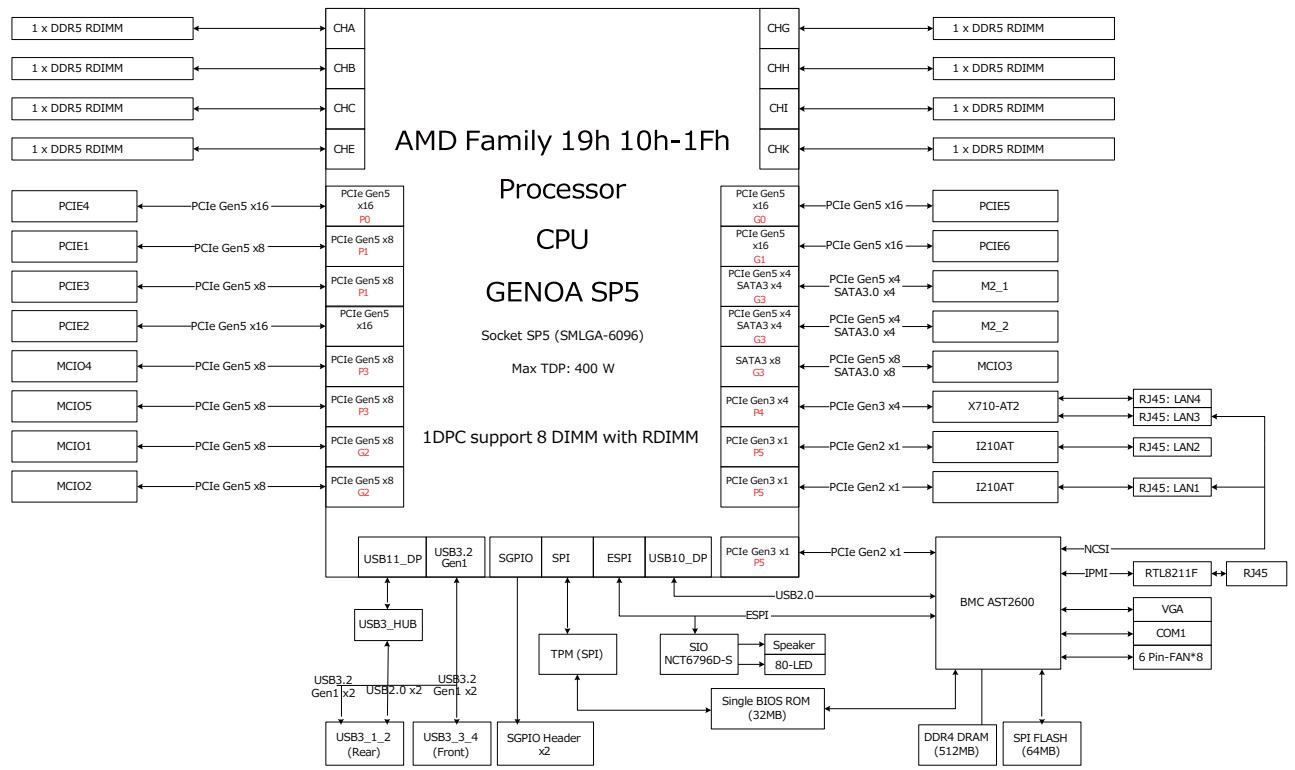
# 3 Functional Block Diagram
![**Central Processor**\n*   **Block:** 'AMD Family 19h 10h-1Fh Processor CPU GENOA SP5'\n*   **Details:** 'Socket SP5 (SMLGA-6096)', 'Max TDP: 400 W', '1DPC support 8 DIMM with RDIMM'\n\n**Memory Connections (Top)**\n*   **Left Channel:** 'CHA', 'CHB', 'CHC', 'CHE' each connect to a '1 x DDR5 RDIMM'.\n*   **Right Channel:** 'CHG', 'CHH', 'CHI', 'CHK' each connect to a '1 x DDR5 RDIMM'.\n\n**Left PCIe Connections**\n*   'PCIE4' connects via 'PCIe Gen5 x16' to 'PCIe Gen5 x16 P0'.\n*   'PCIE1' and 'PCIE3' connect via 'PCIe Gen5 x8' to 'PCIe Gen5 x8 P1'.\n*   'PCIE2' connects via 'PCIe Gen5 x16' to 'PCIe Gen5 x16'.\n*   'MCIO4' and 'MCIO5' connect via 'PCIe Gen5 x8' to 'PCIe Gen5 x8 P3'.\n*   'MCIO1' and 'MCIO2' connect via 'PCIe Gen5 x8' to 'PCIe Gen5 x8 G2'.\n\n**Right PCIe Connections**\n*   'PCIE5' connects via 'PCIe Gen5 x16' to 'PCIe Gen5 x16 G0'.\n*   'PCIE6' connects via 'PCIe Gen5 x16' to 'PCIe Gen5 x16 G1'.\n*   'M2_1' and 'M2_2' connect via 'PCIe Gen5 x4 SATA3.0 x4' to 'PCIe Gen5 x4 G3'.\n*   'MCIO3' connects via 'PCIe Gen5 x8 SATA3.0 x8' to 'SATA3 x8 G3'.\n*   'X710-AT2' connects via 'PCIe Gen3 x4' to 'PCIe Gen3 x4 P4'.\n*   Two 'I210AT' blocks connect via 'PCIe Gen2 x1' to 'PCIe Gen3 x1 P5'.\n\n**Network Ports**\n*   'RJ45: LAN4' and 'RJ45: LAN3' connect to 'X710-AT2'.\n*   'RJ45: LAN2' and 'RJ45: LAN1' connect to the 'I210AT' blocks.\n\n**BMC (Baseboard Management Controller) Section**\n*   **Block:** 'BMC AST2600'\n*   **CPU Connections:** Receives connections from 'USB11_DP', 'USB3.2 Gen1', 'SGPIO', 'SPI', 'ESPI', 'USB10_DP', and 'PCIe Gen3 x1 P5' (via 'PCIe Gen2 x1').\n*   **Peripherals:** Connects to 'VGA', 'COM1', and '6 Pin-FAN*8'.\n*   **Memory:** Connects to 'DDR4 DRAM (512MB)' and 'SPI FLASH (64MB)'.\n*   **Networking:** Connects via 'NCSI' and 'IPMI' to 'RTL8211F', which connects to 'RJ45'.\n*   **SIO Connection:** Connects via 'USB2.0' and 'ESPI' to 'SIO NCT6796D-S'.\n\n**USB & Peripheral Hub**\n*   **Block:** 'USB3_HUB' connects to 'USB11_DP' and 'USB3.2 Gen1' on the CPU side.\n*   **Outputs:** Connects to 'USB3_1_2 (Rear)' and 'USB3_3_4 (Front)' via lines labeled 'USB3.2 Gen1 x2' and 'USB2.0 x2'.\n\n**TPM & BIOS**\n*   **Block:** 'TPM (SPI)' connects to 'SGPIO', 'SPI', and 'ESPI' from the CPU.\n*   **BIOS:** 'TPM (SPI)' and 'SIO NCT6796D-S' connect to 'Single BIOS ROM (32MB)'.\n*   **SIO Peripherals:** 'SIO NCT6796D-S' connects to 'Speaker', '80-LED', and 'Single BIOS ROM (32MB)'.\n*   **Header:** 'SGPIO' connects to 'SGPIO Header x2'.](.isb-tr10-50m-13022-1000-10/6218e868eed0ba4553eee5304fe0c92f1507a633f5a04c2580a3f36440735b8d.jpg)

Figure 1: Functional block diagram

This page intentionally left blank.

# 4 Mechanical Layout

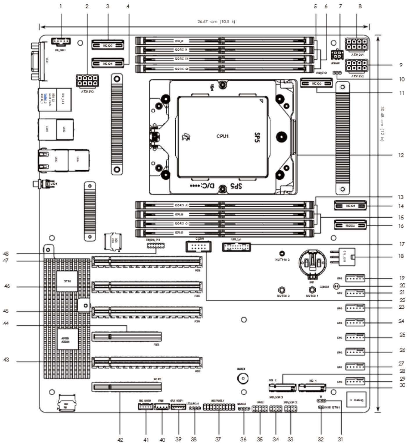
# Motherboard Layout
![26.67 cm (10.5 h)\nATX12V1\nATX12V2\nCPU1 SdS\nDCRJ4\nDCRS H\nDCRS H\nDCRS G\nACWH1\nACWFG1\nATX12V1\nATX12V2\n30.48 cm (12 h)\nUDD\nUSB1\nUSB2\nUSB3\nUSB4\nUSB5\nUSB6\nUSB7\nUSB8\nUSB9\nUSB10\nUSB11\nNUT10 2\nNUT110 2\nNUT10 1\nNUT10 2\nNUT10 2\nNUT10 2\nNUT10 2\nNUT10 2\nNUT10 2\nNUT10 2\nNUT10 2\nNUT10 2\nNUT10 2\nNUT10 2\nNUT10 2\nNUT10 2\nNUT10 2\nNUT10 2\nPCC1\nPCC2\nPCC3\nPCC4\nPCC5\nPCC6\nPCC7\nPCC8\nPCC9\nPCC10\nPCC11\nPCC12\nPCC13\nPCC14\nPCC15\nPCC16\nPCC17\nPCC18\nPCC19\nPCC20\nPCC21\nPCC22\nPCC23\nPCC24\nPCC25\nPCC26\nPCC27\nPCC28\nPCC29\nPCC30\nPCC31\nPCC32\nPCC33\nPCC34\nPCC35\nPCC36\nPCC37\nPCC38\nPCC39\nPCC40\nPCC41\nPCC42\n48 XT10 PCB\n47 XTO PCB\n46 PCB PCB PCB PCB PCB PCB PCB PCB PCB PCB PCB PCB PCB PCB PCB PCB PCB PCB PCB PCB PCB PCB PCB PCB PCB PCB PCB PCB PCB PCB PCB PCB PCB PCB PCB PCB PCB PCB PCB PCB PCB PCB PCB PCB PCB PCB PCB PCB PCB PCB PC8 PTX1 DSB Debug](.isb-tr10-50m-13022-1000-10/f3dafbb33ba6b08e2fec42d90724d17931761ab9af7ccbf5d36e7b25c6de8747.jpg)

Figure 2: Motherboard layout

Table 1: Motherboard layout descriptions

<table><tr><td colspan="2">IO Panel Connectors</td></tr><tr><td>Item</td><td>Description</td></tr><tr><td>1</td><td>PSU SMBus Header (PSU_SMB1)</td></tr><tr><td>2</td><td>ATX 12V Power Connector (ATX12V3)</td></tr><tr><td>3</td><td>Mini Cool Edge IO x8 Connector (MCIO5)</td></tr><tr><td>4</td><td>Mini Cool Edge IO x8 Connector (MCIO4)</td></tr><tr><td>5</td><td>2 x 288-pin DDR5 DIMM Slots (DDR5_H1, DDR5_K1)*</td></tr><tr><td>6</td><td>2 x 288-pin DDR5 DIMM Slots (DDR5_G1, DDR5_I1)*</td></tr><tr><td>7</td><td>ATX Power Connector (ATXPWR1)</td></tr><tr><td>8</td><td>ATX 12V Power Connector (ATX12V1)</td></tr><tr><td>9</td><td>ATX 12V Power Connector (ATX12V2)</td></tr><tr><td>10</td><td>PWM Configuration Header (PWM_CFG1)</td></tr><tr><td>11</td><td>Mini Cool Edge IO x8 Connector (MCIO3)</td></tr><tr><td>12</td><td>AMD Socket SP5 (SM-LGA-6096P) (CPU1)</td></tr><tr><td>13</td><td>2 x 288-pin DDR5 DIMM Slots (DDR5_A1, DDR5_C1)*</td></tr><tr><td>14</td><td>Mini Cool Edge IO x8 Connector (MCIO1)</td></tr><tr><td>15</td><td>2 x 288-pin DDR5 DIMM Slots (DDR5_B1, DDR5_E1)*</td></tr><tr><td>16</td><td>Mini Cool Edge IO x8 Connector (MCIO2)</td></tr><tr><td>17</td><td>USB 3.2 Gen1 Header (USB3_3_4)</td></tr><tr><td>18</td><td>Graphics 12V Power Connector (GFX_12V1)</td></tr><tr><td>19</td><td>System Fan Connector (FAN1)</td></tr><tr><td>20</td><td>Clear CMOS Pad (CLRMOS1)</td></tr><tr><td>21</td><td>System Fan Connector (FAN2)</td></tr><tr><td>22</td><td>COM Port Header (COM1)</td></tr><tr><td>23</td><td>System Fan Connector (FAN3)</td></tr><tr><td>24</td><td>System Fan Connector (FAN4)</td></tr><tr><td>25</td><td>System Fan Connector (FAN5)</td></tr><tr><td>26</td><td>System Fan Connector (FAN6)</td></tr><tr><td>27</td><td>System Fan Connector (FAN7)</td></tr><tr><td>28</td><td>M.2 Socket (M2_2) (Type 2280/22110)</td></tr><tr><td>29</td><td>System Fan Connector (FAN8)</td></tr><tr><td>30</td><td>M.2 Socket (M2_1) (Type 2280)</td></tr><tr><td>31</td><td>Thermal Sensor Header (TR1)</td></tr><tr><td>32</td><td>Non Maskable Interrupt Button (NMI_BTN1)</td></tr><tr><td>33</td><td>SATA SGPIO Connector (SATA_SGPIO2)</td></tr><tr><td>34</td><td>SATA SGPIO Connector (SATA_SGPIO1)</td></tr><tr><td>35</td><td>System Panel Header (PANEL1)</td></tr><tr><td>36</td><td>Speaker Header (SPEAKER1)</td></tr><tr><td>37</td><td>Auxiliary Panel Header (AUX_PANEL1)</td></tr><tr><td>38</td><td>Front LAN LED Connector (LED_LAN3_4)</td></tr><tr><td>39</td><td>Backplane PCI Express Hot-Plug Connector (CPU1_HSBP1)</td></tr><tr><td>40</td><td>Intelligent Platform Management Bus Header (IPMB1)</td></tr><tr><td>41</td><td>BMC SMBus Header (BMC_SMB1)</td></tr><tr><td>42</td><td>PCI Express 5.0 x8 Slot (PCIE1)</td></tr><tr><td>43</td><td>PCI Express 5.0 x16 Slot (PCIE2)</td></tr><tr><td>44</td><td>PCI Express 5.0 x8 Slot (PCIE3)</td></tr><tr><td>45</td><td>PCI Express 5.0 x16 Slot (PCIE4)</td></tr><tr><td>46</td><td>PCI Express 5.0 x16 Slot (PCIE5)</td></tr><tr><td>47</td><td>PCI Express 5.0 x16 Slot (PCIE6)</td></tr><tr><td>48</td><td>SPI TPM Header (TPM_BIOS_PH1)</td></tr></table>

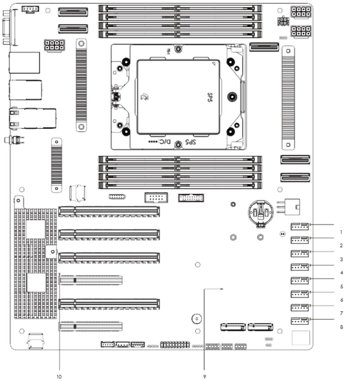
# Onboard LED Indicators

Figure 3: Onboard LED indicators
![SPS\nSDS\n10\n9\n1\n2\n3\n4\n5\n6\n7\n8](.isb-tr10-50m-13022-1000-10/94c54bb6c5452c371a9908934f882fd29c4a5d6caf379aa8f34bae4ccb8516d9.jpg)

Table 2: Onboard LED indicator descriptions

<table><tr><td colspan="2">No.</td><td>Item</td><td>Status Description</td></tr><tr><td>1</td><td>LED_FAN1</td><td>Red</td><td>FAN1 failed</td></tr><tr><td>2</td><td>LED_FAN2</td><td>Red</td><td>FAN2 failed</td></tr><tr><td>3</td><td>LED_FAN3</td><td>Red</td><td>FAN3 failed</td></tr><tr><td>4</td><td>LED_FAN4</td><td>Red</td><td>FAN4 failed</td></tr><tr><td>5</td><td>LED_FAN5</td><td>Red</td><td>FAN5 failed</td></tr><tr><td>6</td><td>LED_FAN6</td><td>Red</td><td>FAN6 failed</td></tr><tr><td>7</td><td>LED_FAN7</td><td>Red</td><td>FAN7 failed</td></tr><tr><td>8</td><td>LED_FAN8</td><td>Red</td><td>FAN8 failed</td></tr><tr><td>9</td><td>SB_PWR1</td><td>Green</td><td>STB PWR ready</td></tr><tr><td>10</td><td>BMC_LED1</td><td>Green</td><td>BMC heartbeat LED</td></tr></table>

# I/O Panel

Figure 4: I/O panel locations
![Diagram showing eight labeled components of an Ethernet port, including a VGA terminal and four Ethernet ports with numbered labels.](.isb-tr10-50m-13022-1000-10/b68ab08bbc9de1b821cadeabaa33e8177aa3c75b2cf775c34241aa611832377b.jpg)

Table 3: I/O panel descriptions

<table><tr><td>No.</td><td>Description</td><td>No.</td><td>Description</td></tr><tr><td>1</td><td>VGA Port (VGA1)</td><td>5</td><td>1G LAN RJ-45 Port (LAN2)**</td></tr><tr><td>2</td><td>USB 3.2 Gen1 Ports (USB3_1_2)</td><td>6</td><td>10G LAN RJ-45 Port (LAN3)***</td></tr><tr><td>3</td><td>IPMI LAN Header (IPMI_LAN1)*</td><td>7</td><td>10G LAN RJ-45 Port (LAN4)***</td></tr><tr><td>4</td><td>1G LAN RJ-45 Port (LAN1, shared NIC)**</td><td>8</td><td>UID Switch (UID1)</td></tr></table>

# 4.3.1 LAN Port LED Indicators

\*There is an LED on each side of IPMI LAN port. Please refer to the table below for the LAN port LED indications.

![ACT/LINK LED\nSPEED LED\nLAN Port](.isb-tr10-50m-13022-1000-10/2451632e6010d9e78a602356edb0bb92559b49dc3cb8673edcc963e8029d1caf.jpg)

IPMI LAN Port LED Indicators

<table><tr><td colspan="2">Activity / Link LED</td><td colspan="2">Speed LED</td></tr><tr><td>Status</td><td>Description</td><td>Status</td><td>Description</td></tr><tr><td>Off</td><td>No Link</td><td>Off</td><td>10Mbps connection or no link</td></tr><tr><td>Blinking Yellow</td><td>Data Activity</td><td>Orange</td><td>100Mbps connection</td></tr><tr><td>On</td><td>Link</td><td>Green</td><td>1Gbps connection</td></tr></table>

\*\*There is an LED on each side of 1G LAN port. Please refer to the table below for the LAN port LED indications.

![ACT/LINK LED\nSPEED LED\nLAN Port](.isb-tr10-50m-13022-1000-10/a9550fd67625e32bae57911340009ef7089d774ff5ddc6dfb4feffecaf683528.jpg)

1G LAN Port LED Indicators

<table><tr><td colspan="2">Activity / Link LED</td><td colspan="2">Speed LED</td></tr><tr><td>Status</td><td>Description</td><td>Status</td><td>Description</td></tr><tr><td>Off</td><td>No Link</td><td>Off</td><td>10Mbps connection or no link</td></tr><tr><td>Blinking Yellow</td><td>Data Activity</td><td>Orange</td><td>100Mbps connection</td></tr><tr><td>On</td><td>Link</td><td>Green</td><td>1Gbps connection</td></tr></table>

\*\*\*There is an LED on each side of 10G LAN port. Please refer to the table below for the LAN port LED indications.

![ACT/LINK LED\nSPEED LED\nLAN Port](.isb-tr10-50m-13022-1000-10/9563e746867e55d1842044015834e1160f7d72650faff41cfb5aad492c5ec3a7.jpg)

10G LAN Port LED Indicators

<table><tr><td colspan="2">Activity / Link LED</td><td colspan="2">Speed LED</td></tr><tr><td>Status</td><td>Description</td><td>Status</td><td>Description</td></tr><tr><td>Off</td><td>No Link</td><td>Off</td><td>100Mbps connection or no link</td></tr><tr><td>Blinking Yellow</td><td>Data Activity</td><td>Orange</td><td>1Gbps connection</td></tr><tr><td>On</td><td>Link</td><td>Green</td><td>10Gbps connection</td></tr></table>

# 5 Installation

This is an CEB form factor (12” x 10.5”, 30.48 x 26.67cm) motherboard. Before installing the motherboard, study the configuration of the chassis to ensure that the motherboard fits into it.

![The image displays a digital icon representing a completed task or document. It features a white sheet of paper with a folded upper-left corner. Faint gray horizontal lines run across the lower portion of the page, suggesting text or a list. A large, thick red checkmark is superimposed diagonally over the center of the paper.](.isb-tr10-50m-13022-1000-10/08a692882a3aa9f868eab5e962a0887e6173091fce8200e1f8cf1207834ad3a4.jpg)
NOTE:

1. Ensure the motherboard battery is installed before unplugging the power cord or installing/removing the motherboard.
2. Before installing or removing any component, ensure that the power is switched off or the power cord is detached from the power supply. Failure to do so may cause severe damage to the motherboard, peripherals, and/or components.

# Screw Holes

Place screws into the holes indicated by circles to secure the motherboard to the chassis.

![The image displays a standard warning symbol consisting of a yellow equilateral triangle with a black border. Inside the triangle, centered, is a large black exclamation point.](.isb-tr10-50m-13022-1000-10/7ba38cb7594b2d7da027c88debe887cd0a6c2fcf6d35cfd34c90edb37055a381.jpg)
CAUTION:

Attention! Before installing this motherboard, be sure to unscrew and remove the standoff at the marked location beneath the motherboard from the chassis to avoid electrical short circuits and damage to the motherboard.

Do not over-tighten the screws. Doing so may damage the motherboard.

![Remove the standoff\nfrom the chassis\nRemove the standoff from\nthe chassis](.isb-tr10-50m-13022-1000-10/b4ccfb4c5bab0292cdb7f6f2dbff1bfa03805cd6ef0343a2efb794f58dac9ce5.jpg)

# Pre-Installation Precautions

Take note of the following precautions before installing motherboard components or change any motherboard settings.

1. Unplug the power cord from the wall socket before touching any components.
2. To avoid damaging the motherboard’s components due to static electricity, NEVER place the motherboard directly on the carpet or the like. Also remember to use a grounded wrist strap or touch a safety grounded object before handling the components.
3. Hold components by the edge and do not touch the ICs.
4. Whenever removing any component, place it on a grounded anti-static pad or in the bag that comes with the component.
5. When placing screws into the screw holes to secure the motherboard to the chassis, please do not overtighten the screws! Doing so may damage the motherboard.

# Installing the CPU

![The image displays a graphical icon featuring a white sheet of paper with horizontal lines representing text. A large, bold red checkmark is superimposed over the center of the paper. The top left corner of the paper is folded down.](.isb-tr10-50m-13022-1000-10/c1d6748cfa601e8679c3cdeb5383d7742679e88a86204f1a37e815d42b8d80c3.jpg)
NOTE:

1. Before inserting the CPU into the socket, please check if the PnP cap is on the socket, if the CPU surface is unclean, or if there are any bent pins in the socket. Do not force to insert the CPU into the socket if above situation is found. Otherwise, the CPU will be seriously damaged.
2. Unplug all power cables before installing the CPU.

![1\n3\n5\nSP6\nD/DC](.isb-tr10-50m-13022-1000-10/3244429802ee9eb28d0572da3d0cf90b39cf123b0e9ac1caba808c1a1cfa169c.jpg)

![2\nSPS\nD/C](.isb-tr10-50m-13022-1000-10/22efb440ddee78b63e3e29f0010faac33d40f05505295745f5b5c43bfe39a2ea.jpg)

![The image displays a technical diagram with three numbered steps (3, 4, and 5) illustrating the assembly or disassembly of a mechanical device.\n\n**Step 3:** Shows a hinged panel labeled 'SP5' being lifted up from a base plate, indicated by a curved yellow arrow. The number '3' appears in a yellow circle at the top.\n\n**Step 4:** Shows the panel 'SP5' lifted further, with arrows indicating it is being removed and moved to the right. A separate inset diagram on the right shows the detached panel, also labeled 'SP5'. The number '4' is in a yellow circle.\n\n**Step 5:** Shows the panel being placed back or adjusted. A yellow arrow points downward. A circular inset on the right provides a close-up view of the assembly, labeling the 'Carrier Frame with CPU' and the 'Rail Frame'. The number '5' is in a yellow circle.](.isb-tr10-50m-13022-1000-10/aadf88a8dede3035e501d7cadfa2bc116114196f605020900cd7ca6df729496f.jpg)
Please make sure that the carier frame with CPU is closely attached to the rail frame while inserting it.

![Technical line drawing of a mechanical assembly with no visible text or symbols](.isb-tr10-50m-13022-1000-10/0b4346434609b7b317e6566655c6e22241bb6344045156620c7dcbc719de1592.jpg)

Install the carrier frame with CPU. Don't separate them.

![7\nSPS\na\nB/C](.isb-tr10-50m-13022-1000-10/24744bd04579f714f536b7d03bc650319148134b986e1b5b2472dc0baf12d77e.jpg)

![8\nS3\nS25\nG10](.isb-tr10-50m-13022-1000-10/9c9394dc71515c15b2112b7927a1f337bf0c1b3595257dd3f09035090d730bae.jpg)

9
![SPS\nI/O/C5\n35\nSPS\n1 6\n4\n3 2\n5\nI/O/C5\nI/O/C5](.isb-tr10-50m-13022-1000-10/94388d779d728149c35d0e7a8723691c9b4fdd9851aff6d968d8770955c894bc.jpg)

10
![194.5.800\nSTEPS 39 BDO 17/06/2015\n2\n3\n4\n5\n6\n7\n8\n9\n10\n11\n12\n13\n14\n15\n16\n17\n18\n19\n20\n21\n22\n23\n24\n25\n26\n27\n28\n29\n30\n31\n32\n33\n34\n35\n36\n37\n38\n39\n40\n41\n42\n43\n44\n45\n46\n47\n48\n49\n50\n51\n52\n53\n54\n55\n56\n57\n58\n59\n60\n61\n62\n63\n64\n65\n66\n67\n68\n69\n70\n71\n72\n73\n74\n75\n76\n77\n78\n79\n80\n81\n82\n83\n84\n85\n86\n87\n88\n89\n90\n91\n92\n93\n94\n95\n96\n97\n98\n99\n100](.isb-tr10-50m-13022-1000-10/d506a0ddf3b4bb962fefa76cb6b070daa0d29fee6fa364ed4ced73fc7ccedaa5.jpg)

Set your torque wrench to 10.8-13.0 in-lb. One fourth a turn each time.
Tighten thescrews inasequential order 1>2>3>4>5>6. Loosen the screws inareyerse order

![Technical diagram of an electronic component with numbered pins and mounting hardware, annotated with Chinese text.](.isb-tr10-50m-13022-1000-10/aff66f314307c0b760139702120c56a225776d444a3a40ee3f02c0b270e8fd14.jpg)

# Installation of Memory Modules (DIMM)

This motherboard provides eight 288-pin DDR5 DIMM slots in two groups, and supports Single Channel Memory Technology.

![This image displays a white document icon with a black outline and a folded top-left corner. Faint gray horizontal lines run across the page, and a large, bold red checkmark is superimposed over the right side.](.isb-tr10-50m-13022-1000-10/6199c6e24a38b8e34a644ccb950c38a210e3a841a3693d4d353e386f78c09f81.jpg)
NOTE:

1. Before installing a memory module, make sure to turn off the computer and unplug the power cord from the power outlet to prevent damage to the memory module.
2. For Eight channel configuration, identical DIMMs must be used (the same brand, speed, size and chip-type).
3. Only DDR5 DIMMs are supported.

Recommended Memory Configurations

<table><tr><td colspan="9">CPU1</td></tr><tr><td></td><td>A1</td><td>B1</td><td>C1</td><td>E1</td><td>G1</td><td>H1</td><td>I1</td><td>K1</td></tr><tr><td>1 DIMM</td><td>V</td><td></td><td></td><td></td><td></td><td></td><td></td><td></td></tr><tr><td>2 DIMMS</td><td>V</td><td></td><td></td><td></td><td>V</td><td></td><td></td><td></td></tr><tr><td>4 DIMMS</td><td>V</td><td></td><td>V</td><td></td><td>V</td><td></td><td>V</td><td></td></tr><tr><td>8 DIMMS</td><td>V</td><td>V</td><td>V</td><td>V</td><td>V</td><td>V</td><td>V</td><td>V</td></tr></table>

The symbol V indicates slots populated.

0
![Isometric line drawing of a mechanical lever or support structure with directional arrows indicating motion (no text or symbols)](.isb-tr10-50m-13022-1000-10/adfd108af01aa24007bcc2c2eb17610d79139ad88b7c561b6f3c7b13f9b77cb2.jpg)

![Illustration of hands assembling a mechanical component with a highlighted section (no text or symbols)](.isb-tr10-50m-13022-1000-10/f0b92395c767431250618a506d48e6b12a2d3a09de43cac5c7e902252b4d1c38.jpg)

③
![Isometric line drawing of a rectangular electronic device with multiple panel slots and directional arrows indicating motion (no text or symbols)](.isb-tr10-50m-13022-1000-10/233dead5dc6ad8c5063a03be2d45a90eb4f8836a964954b72f6f832ce03a2a21.jpg)

# Expansion Slots (PCI Express Slots)

There are six PCI Express slots on this motherboard.

PCIE slots:

PCIE1 (PCIE 5.0 x8 slot, from CPU1) is used for PCI Express x8 lane width cards. PCIE2 (PCIE 5.0 x16 slot, from CPU1) is used for PCI Express x16 lane width cards. PCIE3 (PCIE 5.0 x8 slot, from CPU1) is used for PCI Express x8 lane width cards. PCIE4 (PCIE 5.0 x16 slot, from CPU1) is used for PCI Express x16 lane width cards. PCIE5 (PCIE 5.0 x16 slot, from CPU1) is used for PCI Express x16 lane width cards. PCIE6 (PCIE 5.0 x16 slot, from CPU1) is used for PCI Express x16 lane width cards.

<table><tr><td>Slot</td><td>Generation</td><td>Mechanical</td><td>Electrical</td><td>Source</td></tr><tr><td>PCIE1</td><td>5.0</td><td>x8</td><td>x8</td><td>CPU1</td></tr><tr><td>PCIE2</td><td>5.0</td><td>x16</td><td>x16</td><td>CPU1</td></tr><tr><td>PCIE3</td><td>5.0</td><td>x8</td><td>x8</td><td>CPU1</td></tr><tr><td>PCIE4</td><td>5.0</td><td>x16</td><td>x16</td><td>CPU1</td></tr><tr><td>PCIE5</td><td>5.0</td><td>x16</td><td>x16</td><td>CPU1</td></tr><tr><td>PCIE6</td><td>5.0</td><td>x16</td><td>x16</td><td>CPU1</td></tr></table>

# 5.5.1 Installing an Expansion Card

Step 1. Before installing an expansion card, please make sure that the power supply is switched off or the power cord is unplugged. Please read the documentation of the expansion card and make necessary hardware settings for the card before starting the installation.
Step 2. Remove the system unit cover (if the motherboard is already installed in a chassis).
Step 3. Remove the bracket facing the slot that intending to use. Keep the screws for later use.
Step 4. Align the card connector with the slot and press firmly until the card is completely seated on the slot.
Step 5. Fasten the card to the chassis with screws.
Step 6. Replace the system cover.

# M.2 SSD Module Installation

The M.2 sockets (M2\_1/M2\_2, Key M) support 2280 and 22110 M.2 PCI Express modules, up to Gen5 x4 (32 GT/s x4).

![The image is a black-and-white line drawing featuring a large, horizontal rectangular panel. On the far left edge, there is a small notch. Inside the panel, a smaller vertical rectangle is outlined in the center. On the far right edge, there are several stacked horizontal lines. In the bottom right corner, separate from the panel, is a small icon resembling a key or screw.](.isb-tr10-50m-13022-1000-10/3a1be55234ae621e343e7a5c582954921910e1731492b5b5d12b95018c9c4d0b.jpg)

Step 1: Prepare an M.2 SSD module and the mounting screw.

![Technical diagram showing labeled components of a mechanical or electronic component with parts A and B, including dimension lines and features.](.isb-tr10-50m-13022-1000-10/2d03e1a45f7757b6f919823781cf16785c65a5e6182a661d7e2bb2c69f8938a4.jpg)

Step 2: Depending on the PCB type and length of the M.2 SSD module, select the corresponding nut location.

M2\_1:

<table><tr><td>No.</td><td>1</td></tr><tr><td>Nut Location</td><td>A (NUT80_1)</td></tr><tr><td>PCB Length</td><td>8cm</td></tr><tr><td>Module Type</td><td>Type2280</td></tr></table>

M2\_2:

<table><tr><td>No.</td><td>1</td><td>2</td></tr><tr><td>Nut Location</td><td>A (NUT80_2)</td><td>B (NUT110_2)</td></tr><tr><td>PCB Length</td><td>8cm</td><td>11cm</td></tr><tr><td>Module Type</td><td>Type2280</td><td>Type 22110</td></tr></table>

![The image displays two diagrams labeled **A** and **B** on a white background.\n\n**Diagram B** (on the left) shows a 3D representation of a screw standing upright. Yellow arrows illustrate its mechanics: a curved arrow spirals upward along the threaded shaft indicating rotation, and a straight arrow points vertically upward from the top, indicating linear motion.\n\n**Diagram A** (on the right) shows a top-down view of the screw, depicted as a series of concentric circles representing the threads and the center.](.isb-tr10-50m-13022-1000-10/04c1e2cbf837f60034ae80d473167c3b71281cc12481ee216f125226525142fc.jpg)

![The image is a black and white line drawing depicting a staircase ascending from the bottom left. The stairs are shown with horizontal treads and vertical risers. To the right of the staircase is a tall, vertical rectangular structure, likely representing a wall or the side of a building. The entire structure rests on a horizontal base line. There is no text in the image.](.isb-tr10-50m-13022-1000-10/5af841c052b67380873f5242fcf0a7a06034d7f7e377d94ca073e526ff076095.jpg)

Step 3: Move the standoff according to the module type and length.

If using the default nut, skip Steps 3 and 4 and go directly to Step 5.

Otherwise, release the standoff by hand.

![The image displays a technical diagram illustrating a mechanical action. On the left is a simple 2D top-down view of a ring with a central hole. To its right is a 3D perspective view showing a black ring lying flat on a surface, with a black cylindrical pin positioned above it. Two yellow curved arrows point upwards from the ring towards the pin. Below these illustrations is a long horizontal black line. Beneath the left end of the line is the letter 'B', and beneath the right end is the letter 'A'.](.isb-tr10-50m-13022-1000-10/d2c064a553b7a463d20d45a3ca62da35bdf1cb589b964013e42bf6a84a6590f9.jpg)

![This is a black and white line drawing of a tall, rectangular bookcase or shelving unit. The left side features an open section with multiple horizontal shelves, while the right side is covered by a solid vertical panel or door. The image is presented in an isometric perspective.](.isb-tr10-50m-13022-1000-10/fff0602afb8ed82b44e13fec04cce1409512ae7db36d4c6b0b4efedfd08d05c4.jpg)

Step 4: Peel off the yellow protective film from the nut to be used.

Hand-tighten the standoff into the desired nut location on the motherboard.

![The image displays a three-part technical diagram illustrating an assembly process.\n\n**Top Section:** A rectangular plate is shown with a yellow arrow pointing to the right, indicating insertion into a slot on the side of a vertical bracket. To the left are two components labeled **B** (a washer) and **A** (a bolt with a nut).\n\n**Middle Section:** The rectangular plate is shown inserted into the bracket at an angle. A yellow arc indicates an angle of **20°**. The components **A** and **B** are shown to the left.\n\n**Bottom Section:** The assembly is shown flat. A screw is depicted being inserted into a hole, indicated by a downward yellow arrow and a curved yellow arrow showing rotation. The word **NUT** appears below two holes. To the far left, component **B** is shown.](.isb-tr10-50m-13022-1000-10/75402177e39c6df3bb7d57f44e5859df20688dccba5481a98e6b0fef86dc6794.jpg)
Step 5: Align and gently insert the M.2 SSD module into the M.2 slot. Note that the M.2 SSD module fits only in one orientation.
Step 6: Tighten the screw with a screwdriver to secure the module in place. Do not overtighten the screw, as this may damage the module.

This page intentionally left blank.

# 6 Connector Pinouts and Jumper Settings

# Onboard Headers and Connectors

![The image displays a white document icon featuring a folded upper-right corner. A large red checkmark is centered on the page. Faint grey horizontal lines run across the document, resembling text lines. The image is cropped, showing black borders on the left, bottom, and top edges.](.isb-tr10-50m-13022-1000-10/77b97d000495776060149cd596de51efb5f4bb56f7b6e13669acfbe8f732b563.jpg)
NOTE:

Onboard headers and connectors are NOT jumpers. Do NOT place jumper caps over these headers and connectors. Placing jumper caps over the headers and connectors will cause permanent damage to the motherboard.

# 6.1.1 System Panel Header

(9-Pin PANEL1)

![The image displays a technical diagram of a 3x4 grid of circles, representing pins or mounting holes, with associated labels.\n\n**Top Row:**\nAbove the top row of circles are the labels:\n*   **PLED+** (above the first circle)\n*   **PLED-** (above the second circle)\n*   **PWRBTN#** (above the third circle)\n*   **GND** (above the fourth circle)\n\n**Bottom Row:**\nBelow the bottom row of circles are the labels:\n*   **HDLED+** (below the first circle)\n*   **HDLED-** (below the second circle)\n*   **GND** (below the third circle)\n*   **RESET#** (below the fourth circle)\n\n**Middle Row:**\nThe middle row consists of four unlabeled circles. Vertical lines from the top and bottom labels extend through these middle circles, indicating column alignment.\n\n**Additional Markings:**\n*   The number **1** is visible on the far left side, aligned with the middle row.](.isb-tr10-50m-13022-1000-10/b9e99448f51be20ac2ca3fa1b80e210f0274d8091260c5cfad88e0fd136a01d5.jpg)

Connect the power switch, reset switch, and system status indicators on the chassis to this header according to the pin assignments. Ensure the positive and negative pins are correctly aligned before connecting the cables.

# PWRBTN (Power Switch):

Connect to the power switch on the chassis front panel. Configure the system power-off behavior using the power switch.

# RESET (Reset Switch):

Connect to the reset switch on the chassis front panel. Press the reset switch to restart the computer if it freezes and fails to perform a normal restart.

# PLED (System Power LED):

Connect to the power status indicator on the chassis front panel. The LED is on when the system is operating. The LED is off when the system is in the S4 sleep state or powered off (S5).

# HDLED (Hard Drive Activity LED):

Connect to the hard drive activity LED on the chassis front panel. The LED is on when the hard drive is reading or writing data.

The front panel design may vary by chassis. A front panel module typically consists of a power switch, reset switch, power LED, hard drive activity LED, speaker, etc. When connecting the chassis front panel module to this header, ensure that the wire assignments match the pin assignments correctly.

# 6.1.2 Auxiliary Panel Header

(18-Pin AUX\_PANEL1)

![A\nSMB_AAlert\nSMB_CLK\nGND\nSMB_DATA\n+5VSB\n3VSB\nB\nLAN1_LINK\nLED_PWR\nED_PWR\nLAN2_LINK\nCASEOPEN\nGND\nLOCATORLED1+\nLOCATORLED1-\nLOCATORBTN#\nGND\nSystem Fault LED-\nSystem Fault LED+\nC\nD\nE](.isb-tr10-50m-13022-1000-10/9ba48e1fd2cb815a86a31a5123113e5bc21e5fa238051e57d761b3ee538cb81c.jpg)

This header supports multiple functions on the front panel, including front panel SMB, internet status indicator.

A. Front panel SMBus connecting pin (6-1 pin FPSMB)

This header allows user to connect SMBus (System Management Bus) equipment. It can be used for communication between peripheral equipment in the system, which has slower transmission rates, and power management equipment.

B. Internet status indicator (2-pin LAN1\_LED, LAN2\_LED)

These two 2-pin headers allow user to use the Gigabit internet indicator cable to connect to the LAN status indicator. When this indicator flickers, it means that the internet is properly connected.

C. Chassis intrusion pin (2-pin CHASSIS)

This header is provided for host computer chassis with chassis intrusion detection designs. In addition, it must also work with external detection equipment, such as a chassis intrusion detection sensor or a microswitch. When this function is activated, if any chassis component movement occurs, the sensor will immediately detect it and send a signal to this header, and the system will then record this chassis intrusion event. The default setting is set to the CASEOPEN and GND pin; this function is off.

D. Locator LED (4-pin LOCATOR)

This header is for the locator switch and LED on the front panel.

E. System Fault LED (2-pin LOCATOR)

This header is for the Fault LED on the system.

# 6.1.3 USB 3.2 Gen1 Header

(19-pin USB3\_3\_4)

![Vbus\nIntA_PB_SSRX-\nIntA_PB_SSRX+\nGND\nIntA_PB_SSTX-\nIntA_PB_SSTX+\nGND\nIntA_PB_D-\nIntA_PB_D+\nIntA_PB_D+\nDummy\n1\nVbus\nIntA_PA_SSRX-\nIntA_PA_SSRX+\nGND\nIntA_PA_SSTX-\nIntA_PA_SSTX+\nGND\nIntA_PA_D-\nIntA_PA_D+\nIntA_PA_D+](.isb-tr10-50m-13022-1000-10/3245257989441e219201eaf6d3ee5a6b3065f71ad8f2793e7d86d8ebc4042ae3.jpg)

In addition to the two default USB 3.2

Gen1 ports on the I/O panel, this motherboard includes one USB 3.2 Gen1 header. This USB 3.2 Gen1 header supports two USB 3.2 Gen1 ports.

# 6.1.4 SPI TPM Header

(13-pin TPM\_BIOS\_PH1)

![TPM_CS#\nGND\nRSMRST#\nMISO\nSPI_CS\nSPI_WP\nSPI_PIRQ\nSPI_RST\nMOSH\nSPI_CLK\nX\n+3.3V\nSPI_HOLD](.isb-tr10-50m-13022-1000-10/59445fc3ab3024062cf04b7b4a50828e83fb2a7192a4b418498bb1ce53eb0869.jpg)

This connector supports SPI Trusted Platform Module (TPM) system, which can securely store keys, digital certificates, passwords, and data. A TPM system also helps enhance network security, protects digital identities, and ensures platform integrity.

# 6.1.5 Serial Port Header

(9-pin COM1)
![RRXD1\nDDTR#1\nDDSR#1\nCCTS#1\nRRI#1\nRRTS#1\nGND\nTTXD1\nDDCD#1](.isb-tr10-50m-13022-1000-10/722d1a1f1b8b4e6cd196a4ff85931435f998b965bec6d08e1a3f9a468421a4dc.jpg)

This COM header supports a serial port module.

# 6.1.6 PWM Configuration Header

(3-pin PWM\_CFG1)
![SMB_CLK_VSB\nSMB_DATA_VSB\nGND\n1](.isb-tr10-50m-13022-1000-10/cab41d7b44439f323bafdc8c1f846b86741dc6134888ea82347943e62eb42803.jpg)

This header is used for PWM configurations.

# 6.1.7 Non Maskable Interrupt Button Header (2-Pin NMI\_BTN1)

![The image displays a schematic diagram featuring a square outline containing two circles. To the left of the square is the number '1'. Above the square, the text 'GND' is positioned with a vertical line connecting it to the top of the right circle. Below the square, the text 'CONTROL' is positioned with a vertical line connecting it to the bottom of the left circle.](.isb-tr10-50m-13022-1000-10/2ef2095f0f6da3053281912298133132b1ba02b5b69e597ae8f1ca1830f5ab49.jpg)

Please connect a NMI device to this header.

# 6.1.8 PSU SMBus Header (PSU\_SMB1)

![ALERT\nSMBCLK	+3V\n1\nSMBDATA](.isb-tr10-50m-13022-1000-10/61d5e00b1198a050c060a45887c5fa08f9d983d9e4cafcdcea251079eb75f3d7.jpg)

PSU SMBus monitors the status of the power supply, fan and system temperature.

GND

# 6.1.9 BMC SMB Header

(5-pin BMC\_SMB1)

![1\nBMC_SMB_PRESENT_1_N\nPower\nBMC_SMBCCLK\nGND\nBMC_SMBDATA](.isb-tr10-50m-13022-1000-10/3c9221bbb307c4fadd471bac2e9f5a78b64b1fa2c022887a493f6e83172466ae.jpg)

This header is used for the SMBus devices.

# Backplane PCI Express Hot-Plug Connector

(5-pin CPU1\_ HSBP1)

![CPU_HP_SCL\nCPU_HP_SDA\nP0_HP_ALERT_L\nGND\n+3V\n1](.isb-tr10-50m-13022-1000-10/60c81fe9786bf3fc4a945ff676c0a0a52a6d9af07386be659e3af78fcda10fb2.jpg)

The header is used for the hot plug feature of HDDs on the backplane.

# System Fan Connectors

(6-pin FAN1)

![6 5 4 3 2 1\nGND\n12V(FAN_VOLTAGE)\nFAN_SPEED_SENSOR1\nFAN_SPEED_CONTROL\nFAN_SPEED_SENSOR2\nNC](.isb-tr10-50m-13022-1000-10/fde3cd1a05236e2e4333ef74f58efd83137741829df1ef66d6064edc3f6b0d71.jpg)

Connect fan cables to the fan connectors and match the black wire to the ground pin. All fans support Fan Control.

(Refer to Table1: Motherboard layout descriptions, No. 19) (6-pin FAN2)

(Refer to Table1: Motherboard layout descriptions, No. 21) (6-pin FAN3)

(Refer to Table1: Motherboard layout descriptions, No. 23) (6-pin FAN4)

(Refer to Table1: Motherboard layout descriptions, No. 24) (6-pin FAN5)

(Refer to Table1: Motherboard layout descriptions, No. 25) (6-pin FAN6)

(Refer to Table1: Motherboard layout descriptions, No. 26) (6-pin FAN7)

(Refer to Table1: Motherboard layout descriptions, No. 27) (6-pin FAN8)

# SATA SGPIO Connectors

(7-pin SATA\_SGPIO2)

(7-pin SATA\_SGPIO1)

![SCLOCK\nSLOAD\nGND\n1\nSDATAOUT\nGND](.isb-tr10-50m-13022-1000-10/5d6f04f35a14d29fc73dbded6b2a97764fb7e73a555044129fd029c18251401c.jpg)

These connectors support Serial Link interface for onboard SATA connections.

# Thermal Sensor Header

(3-pin TR1)

![The image shows a schematic symbol for a three-pin connector. It features a rectangular housing containing three circles arranged in a horizontal row. A vertical line extends upward from the left side and another extends upward from the right side. A single vertical line extends downward from the center circle to the text 'GND'.](.isb-tr10-50m-13022-1000-10/97ebff4833a4cf895f08174fd228248b5a9410c2831f505a0807c7a438ccdbf9.jpg)

Please connect the thermal sensor cable to either pin 1-2 or pin 2-3 and the other end to the device which wishing to monitor its temperature.

# ATX Power Connectors

(8-pin ATX12V1)

(8-pin ATX12V2)

(8-pin ATX12V3)

![GND\n1\n4\n5\n8\n12V](.isb-tr10-50m-13022-1000-10/640355c27024347fba5c43f693f41b62c0e59896b0a03130f21771c39e2a9a8b.jpg)

This motherboard provides three ATX power connectors.

# Graphics 12V Power

Connector

Right-angle:

(6-pin GFX\_12V1)

Detective Pin
![The image displays a schematic diagram of a 6-pin connector arranged in a 2x3 grid.\n\n*   **Text:**\n    *   'GND' appears twice at the top, above the left and right columns.\n    *   '6' is inside the top-left square.\n    *   '4' is inside the top-right square.\n    *   '3' is inside the bottom-left square.\n    *   '1' is inside the bottom-right square.\n    *   '+12V' appears at the bottom center.\n\n*   **Visual Elements:**\n    *   Red outlines highlight the left column (squares '6' and '3'), the right column (squares '4' and '1'), and the top-middle square. The bottom-middle square is unoutlined.\n    *   A small black rectangle (likely a key or notch) is positioned above the top-middle square.](.isb-tr10-50m-13022-1000-10/e3c52a570a7db9836d1a005d83923cfb017d32e02e46fd16b114d4390bcff7cc.jpg)

This motherboard provides a 6-pin Graphics 12V power connector. Install the PSU’s power cable to this connector when 4 graphics cards are installed.

# ATX Power Connector

(4-pin ATXPWR1)

![PSON#\nGND\n4 3\n2 1\nATX_+5VSB\nATX_PWROK](.isb-tr10-50m-13022-1000-10/bdce6e2d5fd5a970236bf479cc3419d6f2fd7d294aa497521b6de3bda76d395f.jpg)

The motherboard provides one 4-pin power/signal connector which is a required input for ATX power source.

When using ATX power, it is necessary to use a 24pin-to-4pin power cable to connect between the 24pin power connector of PSU and the ATX12V1, ATX12V2 or

ATX12V3 connector on the motherboard for power supply and signal communication.

# Intelligent Platform Management Bus Header (4-Pin IPMB1)

![IPMB_SDA\nIPMB_SCL\n1\nGND\nNo Connect](.isb-tr10-50m-13022-1000-10/771b36dcf33103a986c22bb5379f9b264da66512f5ba86c46bd8c567675a371d.jpg)

This 4-pin connector is used to provide a cabled baseboard or front panel connection

for value added features and 3rd-party addin cards, such as Emergency Management cards, that provide management features using the IPMB.

# Chassis Speaker Header

(4-Pin SPEAKER1)

Connect the chassis speaker to this header.

DUMMY SPEAKER

![The image displays a schematic symbol labeled '1' on the far left. To the right is a rectangular box divided into four sections, each containing a circle. Vertical lines extend upward from the top of each circle. Below the first circle (leftmost), the text '+5V' is written, and below the third circle, the text 'DUMMY' is written.](.isb-tr10-50m-13022-1000-10/9e4211034a97883b7cb5968dc5534c363c19e474172488539719663e4fc02561.jpg)

# Front LAN LED Connector

(LED\_LAN3-4)

![LAN4_LINK\nLED_PWR\n1](.isb-tr10-50m-13022-1000-10/901a6d6dab49ccb669652d2f880bb15af7e9a41001f0215e5aa398a8940154da.jpg)

This 4-pin connector is used for the front LAN status indicator.

LAN3 LINK LED\_PWR

# Clear CMOS Pad

(CLRCMOS1)

![The image displays a simple black-and-white line drawing. It features a large circle enclosing two solid black shapes. These shapes are oriented vertically and resemble semi-circles or crescents. They are positioned symmetrically, facing each other in the center of the circle, with their straight outer edges facing outward and their curved inner edges facing inward. There is no text visible.](.isb-tr10-50m-13022-1000-10/e4dfd309f8dbd8ca48d65bc5ca274a361dfbbe2eaab299874e725e78002a3bf2.jpg)

This allows user to clear the data in CMOS. To clear CMOS, take out the CMOS battery and short the Clear CMOS Pad.

# MCI) x8 Connectors

![The image displays a simple black-and-white line drawing of nested rectangular shapes. It features a large outer rectangle with a thick border. Inside this outer shape is a slightly smaller rectangle with a thinner border. Within this inner rectangle, there are two distinct sections: a large, wide rectangle at the top and a narrower, smaller rectangle positioned below it in the lower section. There is no text or other markings visible.](.isb-tr10-50m-13022-1000-10/edd7e8b5fd6f3b8e1cb44804dbcda4d777b5d03bb710ca184f81b985b88a8cc2.jpg)

These connectors are used for the PCIE devices.

(MCIO1)

<table><tr><td>Pin</td><td>Signal</td><td>Pin</td><td>Signal</td></tr><tr><td>A1</td><td>GND</td><td>B1</td><td>GND</td></tr><tr><td>A2</td><td>G2_RXP7</td><td>B2</td><td>G2_TXN7</td></tr><tr><td>A3</td><td>G2_RXN7</td><td>B3</td><td>G2_TXP7</td></tr><tr><td>A4</td><td>GND</td><td>B4</td><td>GND</td></tr><tr><td>A5</td><td>G2_RXP6</td><td>B5</td><td>G2_TXN6</td></tr><tr><td>A6</td><td>G2_RXN6</td><td>B6</td><td>G2_TXP6</td></tr><tr><td>A7</td><td>GND</td><td>B7</td><td>GND</td></tr><tr><td>A8</td><td>BP_TYPE</td><td>B8</td><td>SMB_SCL</td></tr><tr><td>A9</td><td>WAKE#</td><td>B9</td><td>SMB_SDA</td></tr><tr><td>A10</td><td>GND</td><td>B10</td><td>GND</td></tr><tr><td>A11</td><td>DP</td><td>B11</td><td>RST0_L</td></tr><tr><td>A12</td><td>DN</td><td>B12</td><td>PRSNT_N</td></tr><tr><td>A13</td><td>GND</td><td>B13</td><td>GND</td></tr><tr><td>A14</td><td>G2_RXP5</td><td>B14</td><td>G2_TXN5</td></tr><tr><td>A15</td><td>G2_RXN5</td><td>B15</td><td>G2_TXP5</td></tr><tr><td>A16</td><td>GND</td><td>B16</td><td>GND</td></tr><tr><td>A17</td><td>G2_RXP4</td><td>B17</td><td>G2_TXN4</td></tr><tr><td>A18</td><td>G2_RXN4</td><td>B18</td><td>G2_TXP4</td></tr><tr><td>A19</td><td>GND</td><td>B19</td><td>GND</td></tr><tr><td>A20</td><td>G2_RXP3</td><td>B20</td><td>G2_TXN3</td></tr><tr><td>A21</td><td>G2_RXN3</td><td>B21</td><td>G2_TXP3</td></tr><tr><td>A22</td><td>GND</td><td>B22</td><td>GND</td></tr><tr><td>A23</td><td>G2_RXP2</td><td>B23</td><td>G2_TXN2</td></tr><tr><td>A24</td><td>G2_RXN2</td><td>B24</td><td>G2_TXP2</td></tr><tr><td>A25</td><td>GND</td><td>B25</td><td>GND</td></tr><tr><td>A26</td><td>BP_TYPE</td><td>B26</td><td>SMB_SCL</td></tr><tr><td>A27</td><td>WAKE#</td><td>B27</td><td>SMB_SDA</td></tr><tr><td>A28</td><td>GND</td><td>B28</td><td>GND</td></tr><tr><td>A29</td><td>DP</td><td>B29</td><td>RST0_L</td></tr><tr><td>A30</td><td>DN</td><td>B30</td><td>PRSNT_N</td></tr><tr><td>A31</td><td>GND</td><td>B31</td><td>GND</td></tr><tr><td>A32</td><td>G2_RXP1</td><td>B32</td><td>G2_TXN1</td></tr><tr><td>A33</td><td>G2_RXN1</td><td>B33</td><td>G2_TXP1</td></tr><tr><td>A34</td><td>GND</td><td>B34</td><td>GND</td></tr><tr><td>A35</td><td>G2_RXP0</td><td>B35</td><td>G2_TXN0</td></tr><tr><td>A36</td><td>G2_RXN0</td><td>B36</td><td>G2_TXP0</td></tr><tr><td>A37</td><td>GND</td><td>B37</td><td>GND</td></tr><tr><td>75</td><td>NP_NC_1</td><td>76</td><td>NP_NC_2</td></tr><tr><td>77</td><td>PGND_1</td><td>78</td><td>PGND_3</td></tr><tr><td>79</td><td>PGND_2</td><td>80</td><td>PGND_4</td></tr></table>

(MCIO2)

<table><tr><td>Pin</td><td>Definition</td><td>Pin</td><td>Definition</td></tr><tr><td>A1</td><td>GND</td><td>B1</td><td>GND</td></tr><tr><td>A2</td><td>G2_RXP15</td><td>B2</td><td>G2_TXN15</td></tr><tr><td>A3</td><td>G2_RXN15</td><td>B3</td><td>G2_TXP15</td></tr><tr><td>A4</td><td>GND</td><td>B4</td><td>GND</td></tr><tr><td>A5</td><td>G2_RXP14</td><td>B5</td><td>G2_TXN14</td></tr><tr><td>A6</td><td>G2_RXN14</td><td>B6</td><td>G2_TXP14</td></tr><tr><td>A7</td><td>GND</td><td>B7</td><td>GND</td></tr><tr><td>A8</td><td>BP_TYPE</td><td>B8</td><td>SMB_SCL</td></tr><tr><td>A9</td><td>WAKE#</td><td>B9</td><td>SMB_SDA</td></tr><tr><td>A10</td><td>GND</td><td>B10</td><td>GND</td></tr><tr><td>A11</td><td>DP</td><td>B11</td><td>RST0_L</td></tr><tr><td>A12</td><td>DN</td><td>B12</td><td>PRSNT_N</td></tr><tr><td>A13</td><td>GND</td><td>B13</td><td>GND</td></tr><tr><td>A14</td><td>G2_RXP13</td><td>B14</td><td>G2_TXN13</td></tr><tr><td>A15</td><td>G2_RXN13</td><td>B15</td><td>G2_TXP13</td></tr><tr><td>A16</td><td>GND</td><td>B16</td><td>GND</td></tr><tr><td>A17</td><td>G2_RXP12</td><td>B17</td><td>G2_TXN12</td></tr><tr><td>A18</td><td>G2_RXN12</td><td>B18</td><td>G2_TXP12</td></tr><tr><td>A19</td><td>GND</td><td>B19</td><td>GND</td></tr><tr><td>A20</td><td>G2_RXP11</td><td>B20</td><td>G2_TXN11</td></tr><tr><td>A21</td><td>G2_RXN11</td><td>B21</td><td>G2_TXP11</td></tr><tr><td>A22</td><td>GND</td><td>B22</td><td>GND</td></tr><tr><td>A23</td><td>G2_RXP10</td><td>B23</td><td>G2_TXN10</td></tr><tr><td>A24</td><td>G2_RXN10</td><td>B24</td><td>G2_TXP10</td></tr><tr><td>A25</td><td>GND</td><td>B25</td><td>GND</td></tr><tr><td>A26</td><td>BP_TYPE</td><td>B26</td><td>SMB_SCL</td></tr><tr><td>A27</td><td>WAKE#</td><td>B27</td><td>SMB_SDA</td></tr><tr><td>A28</td><td>GND</td><td>B28</td><td>GND</td></tr><tr><td>A29</td><td>DP</td><td>B29</td><td>RST0_L</td></tr><tr><td>A30</td><td>DN</td><td>B30</td><td>PRSNT_N</td></tr><tr><td>A31</td><td>GND</td><td>B31</td><td>GND</td></tr><tr><td>A32</td><td>G2_RXP9</td><td>B32</td><td>G2_TXN9</td></tr><tr><td>A33</td><td>G2_RXN9</td><td>B33</td><td>G2_TXP9</td></tr><tr><td>A34</td><td>GND</td><td>B34</td><td>GND</td></tr><tr><td>A35</td><td>G2_RXP8</td><td>B35</td><td>G2_TXN8</td></tr><tr><td>A36</td><td>G2_RXN8</td><td>B36</td><td>G2_TXP8</td></tr><tr><td>A37</td><td>GND</td><td>B37</td><td>GND</td></tr><tr><td>75</td><td>NP_NC_1</td><td>76</td><td>NP_NC_2</td></tr><tr><td>77</td><td>PGND_1</td><td>78</td><td>PGND_3</td></tr><tr><td>79</td><td>PGND_2</td><td>80</td><td>PGND_4</td></tr></table>

(MICIO3)

<table><tr><td>Pin</td><td>Definition</td><td>Pin</td><td>Definition</td></tr><tr><td>A1</td><td>GND</td><td>B1</td><td>GND</td></tr><tr><td>A2</td><td>G3_RXP0</td><td>B2</td><td>G3_TXP0</td></tr><tr><td>A3</td><td>G3_RXN0</td><td>B3</td><td>G3_TXN0</td></tr><tr><td>A4</td><td>GND</td><td>B4</td><td>GND</td></tr><tr><td>A5</td><td>G3_RXP1</td><td>B5</td><td>G3_TXP1</td></tr><tr><td>A6</td><td>G3_RXN1</td><td>B6</td><td>G3_TXN1</td></tr><tr><td>A7</td><td>GND</td><td>B7</td><td>GND</td></tr><tr><td>A8</td><td>BP_TYPE</td><td>B8</td><td>SMB_SCL</td></tr><tr><td>A9</td><td>WAKE#</td><td>B9</td><td>SMB_SDA</td></tr><tr><td>A10</td><td>GND</td><td>B10</td><td>GND</td></tr><tr><td>A11</td><td>DP</td><td>B11</td><td>RST0_L</td></tr><tr><td>A12</td><td>DN</td><td>B12</td><td>PRSNT_N</td></tr><tr><td>A13</td><td>GND</td><td>B13</td><td>GND</td></tr><tr><td>A14</td><td>G3_RXP2</td><td>B14</td><td>G3_TXP2</td></tr><tr><td>A15</td><td>G3_RXN2</td><td>B15</td><td>G3_TXN2</td></tr><tr><td>A16</td><td>GND</td><td>B16</td><td>GND</td></tr><tr><td>A17</td><td>G3_RXP3</td><td>B17</td><td>G3_TXP3</td></tr><tr><td>A18</td><td>G3_RXN3</td><td>B18</td><td>G3_TXN3</td></tr><tr><td>A19</td><td>GND</td><td>B19</td><td>GND</td></tr><tr><td>A20</td><td>G3_RXP4</td><td>B20</td><td>G3_TXP4</td></tr><tr><td>A21</td><td>G3_RXN4</td><td>B21</td><td>G3_TXN4</td></tr><tr><td>A22</td><td>GND</td><td>B22</td><td>GND</td></tr><tr><td>A23</td><td>G3_RXP5</td><td>B23</td><td>G3_TXP5</td></tr><tr><td>A24</td><td>G3_RXN5</td><td>B24</td><td>G3_TXN5</td></tr><tr><td>A25</td><td>GND</td><td>B25</td><td>GND</td></tr><tr><td>A26</td><td>BP_TYPE</td><td>B26</td><td>SMB_SCL</td></tr><tr><td>A27</td><td>WAKE#</td><td>B27</td><td>SMB_SDA</td></tr><tr><td>A28</td><td>GND</td><td>B28</td><td>GND</td></tr><tr><td>A29</td><td>DP</td><td>B29</td><td>RST0_L</td></tr><tr><td>A30</td><td>DN</td><td>B30</td><td>PRSNT_N</td></tr><tr><td>A31</td><td>GND</td><td>B31</td><td>GND</td></tr><tr><td>A32</td><td>G3_RXP6</td><td>B32</td><td>G3_TXP6</td></tr><tr><td>A33</td><td>G3_RXN6</td><td>B33</td><td>G3_TXN6</td></tr><tr><td>A34</td><td>GND</td><td>B34</td><td>GND</td></tr><tr><td>A35</td><td>G3_RXP7</td><td>B35</td><td>G3_TXP7</td></tr><tr><td>A36</td><td>G3_RXN7</td><td>B36</td><td>G3_TXN7</td></tr><tr><td>A37</td><td>GND</td><td>B37</td><td>GND</td></tr><tr><td>75</td><td>NP_NC_1</td><td>76</td><td>NP_NC_2</td></tr><tr><td>77</td><td>PGND_1</td><td>78</td><td>PGND_3</td></tr><tr><td>79</td><td>PGND_2</td><td>80</td><td>PGND_4</td></tr></table>

(MCIO4)

<table><tr><td>Pin</td><td>Definition</td><td>Pin</td><td>Definition</td></tr><tr><td>A1</td><td>GND</td><td>B1</td><td>GND</td></tr><tr><td>A2</td><td>P3_RXN0</td><td>B2</td><td>P3_TXP0</td></tr><tr><td>A3</td><td>P3_RXP0</td><td>B3</td><td>P3_TXN0</td></tr><tr><td>A4</td><td>GND</td><td>B4</td><td>GND</td></tr><tr><td>A5</td><td>P3_RXN1</td><td>B5</td><td>P3_TXP1</td></tr><tr><td>A6</td><td>P3_RXP1</td><td>B6</td><td>P3_TXN1</td></tr><tr><td>A7</td><td>GND</td><td>B7</td><td>GND</td></tr><tr><td>A8</td><td>BP_TYPE</td><td>B8</td><td>SMB_SCL</td></tr><tr><td>A9</td><td>WAKE#</td><td>B9</td><td>SMB_SDA</td></tr><tr><td>A10</td><td>GND</td><td>B10</td><td>GND</td></tr><tr><td>A11</td><td>DP</td><td>B11</td><td>RST1_L</td></tr><tr><td>A12</td><td>DN</td><td>B12</td><td>PRSNT_N</td></tr><tr><td>A13</td><td>GND</td><td>B13</td><td>GND</td></tr><tr><td>A14</td><td>P3_RXN2</td><td>B14</td><td>P3_TXP2</td></tr><tr><td>A15</td><td>P3_RXP2</td><td>B15</td><td>P3_TXN2</td></tr><tr><td>A16</td><td>GND</td><td>B16</td><td>GND</td></tr><tr><td>A17</td><td>P3_RXN3</td><td>B17</td><td>P3_TXP3</td></tr><tr><td>A18</td><td>P3_RXP3</td><td>B18</td><td>P3_TXN3</td></tr><tr><td>A19</td><td>GND</td><td>B19</td><td>GND</td></tr><tr><td>A20</td><td>P3_RXN4</td><td>B20</td><td>P3_TXP4</td></tr><tr><td>A21</td><td>P3_RXP4</td><td>B21</td><td>P3_TXN4</td></tr><tr><td>A22</td><td>GND</td><td>B22</td><td>GND</td></tr><tr><td>A23</td><td>P3_RXN5</td><td>B23</td><td>P3_TXP5</td></tr><tr><td>A24</td><td>P3_RXP5</td><td>B24</td><td>P3_TXN5</td></tr><tr><td>A25</td><td>GND</td><td>B25</td><td>GND</td></tr><tr><td>A26</td><td>BP_TYPE</td><td>B26</td><td>SMB_SCL</td></tr><tr><td>A27</td><td>WAKE#</td><td>B27</td><td>SMB_SDA</td></tr><tr><td>A28</td><td>GND</td><td>B28</td><td>GND</td></tr><tr><td>A29</td><td>DP</td><td>B29</td><td>RST1_L</td></tr><tr><td>A30</td><td>DN</td><td>B30</td><td>PRSNT_N</td></tr><tr><td>A31</td><td>GND</td><td>B31</td><td>GND</td></tr><tr><td>A32</td><td>P3_RXN6</td><td>B32</td><td>P3_TXP6</td></tr><tr><td>A33</td><td>P3_RXP6</td><td>B33</td><td>P3_TXN6</td></tr><tr><td>A34</td><td>GND</td><td>B34</td><td>GND</td></tr><tr><td>A35</td><td>P3_RXN7</td><td>B35</td><td>P3_TXP7</td></tr><tr><td>A36</td><td>P3_RXP7</td><td>B36</td><td>P3_TXN7</td></tr><tr><td>A37</td><td>GND</td><td>B37</td><td>GND</td></tr><tr><td>75</td><td>NP_NC_1</td><td>76</td><td>NP_NC_2</td></tr><tr><td>77</td><td>PGND_1</td><td>78</td><td>PGND_3</td></tr><tr><td>79</td><td>PGND_2</td><td>80</td><td>PGND_4</td></tr></table>

(MCIO5)

<table><tr><td>Pin</td><td>Definition</td><td>Pin</td><td>Definition</td></tr><tr><td>A1</td><td>GND</td><td>B1</td><td>GND</td></tr><tr><td>A2</td><td>P3_RXN8</td><td>B2</td><td>P3_TXP8</td></tr><tr><td>A3</td><td>P3_RXP8</td><td>B3</td><td>P3_TXN8</td></tr><tr><td>A4</td><td>GND</td><td>B4</td><td>GND</td></tr><tr><td>A5</td><td>P3_RXN9</td><td>B5</td><td>P3_TXP9</td></tr><tr><td>A6</td><td>P3_RXP9</td><td>B6</td><td>P3_TXN9</td></tr><tr><td>A7</td><td>GND</td><td>B7</td><td>GND</td></tr><tr><td>A8</td><td>BP_TYPE</td><td>B8</td><td>SMB_SCL</td></tr><tr><td>A9</td><td>WAKE#</td><td>B9</td><td>SMB_SDA</td></tr><tr><td>A10</td><td>GND</td><td>B10</td><td>GND</td></tr><tr><td>A11</td><td>DP</td><td>B11</td><td>RST1_L</td></tr><tr><td>A12</td><td>DN</td><td>B12</td><td>PRSNT_N</td></tr><tr><td>A13</td><td>GND</td><td>B13</td><td>GND</td></tr><tr><td>A14</td><td>P3_RXN10</td><td>B14</td><td>P3_TXP10</td></tr><tr><td>A15</td><td>P3_RXP10</td><td>B15</td><td>P3_TXN10</td></tr><tr><td>A16</td><td>GND</td><td>B16</td><td>GND</td></tr><tr><td>A17</td><td>P3_RXN11</td><td>B17</td><td>P3_TXP11</td></tr><tr><td>A18</td><td>P3_RXP11</td><td>B18</td><td>P3_TXN11</td></tr><tr><td>A19</td><td>GND</td><td>B19</td><td>GND</td></tr><tr><td>A20</td><td>P3_RXN12</td><td>B20</td><td>P3_TXP12</td></tr><tr><td>A21</td><td>P3_RXP12</td><td>B21</td><td>P3_TXN12</td></tr><tr><td>A22</td><td>GND</td><td>B22</td><td>GND</td></tr><tr><td>A23</td><td>P3_RXN13</td><td>B23</td><td>P3_TXP13</td></tr><tr><td>A24</td><td>P3_RXP13</td><td>B24</td><td>P3_TXN13</td></tr><tr><td>A25</td><td>GND</td><td>B25</td><td>GND</td></tr><tr><td>A26</td><td>BP_TYPE</td><td>B26</td><td>SMB_SCL</td></tr><tr><td>A27</td><td>WAKE#</td><td>B27</td><td>SMB_SDA</td></tr><tr><td>A28</td><td>GND</td><td>B28</td><td>GND</td></tr><tr><td>A29</td><td>DP</td><td>B29</td><td>RST1_L</td></tr><tr><td>A30</td><td>DN</td><td>B30</td><td>PRSNT_N</td></tr><tr><td>A31</td><td>GND</td><td>B31</td><td>GND</td></tr><tr><td>A32</td><td>P3_RXN14</td><td>B32</td><td>P3_TXP14</td></tr><tr><td>A33</td><td>P3_RXP14</td><td>B33</td><td>P3_TXN14</td></tr><tr><td>A34</td><td>GND</td><td>B34</td><td>GND</td></tr><tr><td>A35</td><td>P3_RXN15</td><td>B35</td><td>P3_TXP15</td></tr><tr><td>A36</td><td>P3_RXP15</td><td>B36</td><td>P3_TXN15</td></tr><tr><td>A37</td><td>GND</td><td>B37</td><td>GND</td></tr><tr><td>75</td><td>NP_NC_1</td><td>76</td><td>NP_NC_2</td></tr><tr><td>77</td><td>PGND_1</td><td>78</td><td>PGND_3</td></tr><tr><td>79</td><td>PGND_2</td><td>80</td><td>PGND_4</td></tr></table>

# ATX PSU Power Connections

This motherboard supports ATX power input. Please refer to the table below for the required connections between the motherboard and the power supply.

![The diagram is titled with a black header block labeled **'ATX PSU'**. Below this is a central white block labeled **'PSU'**.\n\nTwo lines extend downward from the 'PSU' block:\n1.  The left line connects to a block with an 8-pin grid layout, labeled below as **'12V 8pin'**.\n2.  The right line connects to a block with a 4-pin grid layout, labeled below as **'ATX 4pin'**.\n\nNext to the right connection line, there is an annotation reading **'(using supplied 24pin-to-4pin Converter Cable)'** with a curved arrow pointing toward the line.](.isb-tr10-50m-13022-1000-10/4d09146d93740bf696821e0f09a67873a6b17f4da7220bd8000ecb76446c9548.jpg)

The following diagram illustrates how to connect the bundled ATX 24pin-to-4pin converter cable.

![24pin-to-4pin\nConverter Cable\n* Make sure the latch and the socket\nare aligned in the right direction.](.isb-tr10-50m-13022-1000-10/e1ddf11841481b787e95b753887d00599322f4da0f80c97f0ccd47bf5c247338.jpg)

# Dr. Debug

Dr. Debug is used to provide code information, making troubleshooting even easier. Please refer to the diagrams below for instructions on reading the Dr. Debug codes.

<table><tr><td>Code</td><td>Description</td></tr><tr><td>0x1</td><td>PEI_CORE_STARTED</td></tr><tr><td>0x11</td><td>PEI_CAR_CPU_INIT</td></tr><tr><td>0x15</td><td>PEI_CAR_NB_INIT</td></tr><tr><td>0x19</td><td>PEI_CAR_SB_INIT</td></tr><tr><td>0x31</td><td>PEI_MEMORY_INSTALLED</td></tr><tr><td>0x32</td><td>PEI_CPU_INIT</td></tr><tr><td>0x33</td><td>PEI_CPU_CACHE_INIT</td></tr><tr><td>0x34</td><td>PEI_CPU_AP_INIT</td></tr><tr><td>0x35</td><td>PEI_CPU_BSP_SELECT</td></tr><tr><td>0x36</td><td>PEI_CPU_SMM_INIT</td></tr><tr><td>0x37</td><td>PEI_MEM_NB_INIT</td></tr><tr><td>0x3B</td><td>PEI_MEM_SB_INIT</td></tr><tr><td>0x4F</td><td>PEI_DXE_IPL_STARTED</td></tr><tr><td>0x60</td><td>DXE_CORE_STARTED</td></tr><tr><td>0x61</td><td>DXE_NVRAM_INIT</td></tr><tr><td>0x62</td><td>DXE_SBRUN_INIT</td></tr><tr><td>0x63</td><td>DXE_CPU_INIT</td></tr><tr><td>0x68</td><td>DXE_NB_HB_INIT</td></tr><tr><td>0x69</td><td>DXE_NB_INIT</td></tr><tr><td>0x6A</td><td>DXE_NB_SMM_INIT</td></tr><tr><td>0x70</td><td>DXE_SB_INIT</td></tr><tr><td>0x71</td><td>DXE_SB_SMM_INIT</td></tr><tr><td>0x72</td><td>DXE_SB_DEVICES_INIT</td></tr><tr><td>0x78</td><td>DXE ACPI_INIT</td></tr><tr><td>0x79</td><td>DXE_CSM_INIT</td></tr><tr><td>0x90</td><td>DXE_BDS_STARTED</td></tr><tr><td>0x91</td><td>DXE_BDS_CONNECT_DRIVERS</td></tr><tr><td>0x92</td><td>DXE_PCI_BUS_BEGIN</td></tr><tr><td>0x93</td><td>DXE_PCI_BUS_HPC_INIT</td></tr><tr><td>0x94</td><td>DXE_PCI_BUS_ENUM</td></tr><tr><td>0x95</td><td>DXE_PCI_BUS_REQUEST_RESOURCES</td></tr><tr><td>0x96</td><td>DXE_PCI_BUS_ASSIGN_RESOURCES</td></tr><tr><td>0x97</td><td>DXE_CON_OUT_CONNECT</td></tr><tr><td>0x98</td><td>DXE_CON_IN_CONNECT</td></tr><tr><td>0x99</td><td>DXE_SIO_INIT</td></tr><tr><td>0x9A</td><td>DXE_USB_BEGIN</td></tr><tr><td>0x9B</td><td>DXE_USB_RESET</td></tr><tr><td>0x9C</td><td>DXE_USB_DETECT</td></tr><tr><td>0x9D</td><td>DXE_USB_ENABLE</td></tr><tr><td>0xA0</td><td>DXE_IDE_BEGIN</td></tr><tr><td>0xA1</td><td>DXE_IDE_RESET</td></tr><tr><td>0xA2</td><td>DXE_IDE_DETECT</td></tr><tr><td>0xA3</td><td>DXE_IDE_ENABLE</td></tr><tr><td>0xA4</td><td>DXE_SCSI_BEGIN</td></tr><tr><td>0xA5</td><td>DXE_SCSI_RESET</td></tr><tr><td>0xA6</td><td>DXE_SCSI_DETECT</td></tr><tr><td>0xA7</td><td>DXE_SCSI_ENABLE</td></tr><tr><td>0xA8</td><td>DXE_SETUP_VERIFYING_PASSWORD</td></tr><tr><td>0xA9</td><td>DXE_SETUP_START</td></tr><tr><td>0xAB</td><td>DXE_SETUP_INPUT_WAIT</td></tr><tr><td>0xAD</td><td>DXE_READY_TO_BOOT</td></tr><tr><td>0xAE</td><td>DXE_LEGACY_BOOT</td></tr><tr><td>0xAF</td><td>DXE_EXIT_BOOT_SERVICES</td></tr><tr><td>0xB0</td><td>RT_SET_VIRTUAL_ADDRESS_MAP_BEGIN</td></tr><tr><td>0xB1</td><td>RT_SET_VIRTUAL_ADDRESS_MAP_END</td></tr><tr><td>0xB2</td><td>DXE_LEGACY_OPROM_INIT</td></tr><tr><td>0xB3</td><td>DXE_RESET_SYSTEM</td></tr><tr><td>0xB4</td><td>DXE_USB_HOTPLUG</td></tr><tr><td>0xB5</td><td>DXE_PCI_BUS_HOTPLUG</td></tr><tr><td>0xB6</td><td>DXE_NVRAM_CLEANUP</td></tr><tr><td>0xB7</td><td>DXE_CONFIGURATION_RESET</td></tr><tr><td>0xF0</td><td>PEI_RECOVERY_AUTO</td></tr><tr><td>0xF1</td><td>PEI_RECOVERY_USER</td></tr><tr><td>0xF2</td><td>PEI_RECOVERY_STARTED</td></tr><tr><td>0xF3</td><td>PEI_RECOVERY_CAPSULE_FOUND</td></tr><tr><td>0xF4</td><td>PEI_RECOVERY_CAPSULE_LOADED</td></tr><tr><td>0xE0</td><td>PEI_S3_STARTED</td></tr><tr><td>0xE1</td><td>PEI_S3_BOOT_SCRIPT</td></tr><tr><td>0xE2</td><td>PEI_S3_VIDEO_REPOST</td></tr><tr><td>0xE3</td><td>PEI_S3_OS_WAKE</td></tr><tr><td>0x50</td><td>PEI_MEMORY_INVALID_TYPE</td></tr><tr><td>0x53</td><td>PEI_MEMORY_NOT_DETECTED</td></tr><tr><td>0x55</td><td>PEI_MEMORY_NOT_INSTALLED</td></tr><tr><td>0x57</td><td>PEI_CPU_MISMATCH</td></tr><tr><td>0x58</td><td>PEI_CPU_SELF_TEST_FAILED</td></tr><tr><td>0x59</td><td>PEI_CPU_NO_MICROCODE</td></tr><tr><td>0x5A</td><td>PEI_CPU_ERROR</td></tr><tr><td>0x5B</td><td>PEI_RESET_NOT_AVAILABLE</td></tr><tr><td>0xD0</td><td>DXE_CPU_ERROR</td></tr><tr><td>0xD1</td><td>DXE_NB_ERROR</td></tr><tr><td>0xD2</td><td>DXE_SB_ERROR</td></tr><tr><td>0xD3</td><td>DXE_ARCH_PROTOCOL_NOT_AVAILABLE</td></tr><tr><td>0xD4</td><td>DXE_PCI_BUS_OUT_OF_RESOURCES</td></tr><tr><td>0xD5</td><td>DXE_LEGACY_OPROM_NO_SPACE</td></tr><tr><td>0xD6</td><td>DXE_NO_CON_OUT</td></tr><tr><td>0xD7</td><td>DXE_NO_CON_IN</td></tr><tr><td>0xD8</td><td>DXE_INVALID_PASSWORD</td></tr><tr><td>0xD9</td><td>DXE_BOOT_OPTION_LOAD_ERROR</td></tr><tr><td>0xDA</td><td>DXE_BOOT_OPTION_FAILED</td></tr><tr><td>0xDB</td><td>DXE_FLASH_UPDATE_FAILED</td></tr><tr><td>0xDC</td><td>DXE_RESET_NOT_AVAILABLE</td></tr><tr><td>0xE8</td><td>PEI_MEMORY_S3_RESUME_FAILED</td></tr><tr><td>0xE9</td><td>PEI_S3_RESUME_PPI_NOT_FOUND</td></tr><tr><td>0xEA</td><td>PEI_S3_BOOT_SCRIPT_ERROR</td></tr><tr><td>0xEB</td><td>PEI_S3_OS_WAKE_ERROR</td></tr></table>

# LEDs and Switches

With the UID button, users can locate the operating server from behind a rack of servers.

# 6.4.1 Unit Identification Purpose

LED/Switch (UID1)

![A black and white line drawing of a square. Inside the square is a large circle. Inside the large circle is a smaller, concentric circle.](.isb-tr10-50m-13022-1000-10/59d75b852f47b853ef4524a005eef35677de1b0b68bd90559362f08d0626bca1.jpg)

When the UID button on the front or rear panel is pressed, the corresponding front or rear blue UID LED indicator will turn on. Press the UID button again to turn off the indicator.

# Dual LAN and Teaming Operation Guide

Dual LAN with Teaming enabled on this motherboard allows two individual connections to function as a single connection, doubling the transmission bandwidth, improving data transfer efficiency, and enhancing the quality of transmitted distant images. Fault tolerance on the dual LAN network prevents downtime by transferring the workload from a failed port to a functioning port.

![The image displays a white document icon with a folded top-right corner and faint gray horizontal lines resembling text. A large, bold red checkmark is superimposed over the center of the document.](.isb-tr10-50m-13022-1000-10/955b0bd0fafc26b107ee5437338fc3a760d44542ba4a3c77bb9e3e6f330c9d57.jpg)
NOTE:

The speed of transmission is subject to the actual network environment or status even with Teaming enabled.

Before setting up Teaming, make sure that the switch (or router) supports Teaming (IEEE 802.3ad Link Aggregation) and specify a preferred adapter in Intel PROSet. Under normal conditions, the primary adapter handles all non-TCP/IP traffic. The secondary adapter receives fallback traffic if the primary fails. If the preferred primary adapter fails and is later restored to an active status, control is automatically switched back to the preferred primary adapter.

Step 1

From Device Manager, open the properties of a team connection.

Step 2

Click the Settings tab.

Step 3

Click the Modify Team button.

Step 4

Select the adapter that wants to be the primary adapter and click the Set Primary button.

The software will choose an adapter of the highest capability (model and speed) to act as the default primary upon not specify a preferred primary adapter. If a failover occurs, another adapter becomes the primary. The adapter will, however, rejoin the team as a non-primary.

This page intentionally left blank.

# 7 BIOS Settings

This section explains how to use the BIOS SETTINGS UTILITY to configure the system. The UEFI chip on the motherboard stores the BIOS SETTINGS UTILITY. Run the UEFI SETUP UTILITY when starting up the computer. Please press &lt;F2&gt; or &lt;Del&gt; during the Power-On-Self-Test (POST) to enter the BIOS SETTINGS UTILITY; otherwise, POST will continue with its test routines.

Restart the system by pressing &lt;Ctrl&gt; + &lt;Alt&gt; + &lt;Delete&gt; to enter the UEFI SETUP UTI LITY after POST, or by pressing the reset button on the system chassis. This allows users to restart by turning the system off and then back on.

![The image displays a graphic icon of a white document page with black horizontal lines representing text. Overlaid on the page is a large, thick red checkmark that angles upward from left to right.](.isb-tr10-50m-13022-1000-10/b1817a3edbd27cd9a4594961e73e926071f017c5c9c33ccca2321254fcbe678b.jpg)
NOTE:

Because the UEFI software is constantly being updated, the following UEFI setup screens and descriptions are for reference purpose only, and they may not exactly match actual displayed item.

# 7.1.1 BIOS Menu Bar

The top of the screen has a menu bar with the following selections:

<table><tr><td>Item</td><td>Description</td></tr><tr><td>Main</td><td>To set up the system time/date information</td></tr><tr><td>Advanced</td><td>To set up the advanced UEFI features</td></tr><tr><td>Server Mgmt.</td><td>To manage the server</td></tr><tr><td>Event Logs</td><td>For event log configuration</td></tr><tr><td>Security</td><td>To set up the security features</td></tr><tr><td>Boot</td><td>To set up the default system device to locate and load the Operating System</td></tr><tr><td>Exit</td><td>To exit the current screen or the UEFI SETUP UTILITY</td></tr></table>

Use &lt; &gt; key or &lt; &gt; key to choose among the selections on the menu bar, and then press &lt;Enter&gt; to get into the sub screen.

# 7.1.2 Navigation Keys

Please check the following table for the function description of each navigation key.

<table><tr><td>Navigation Key(s)</td><td>Function Description</td></tr><tr><td>← / →</td><td>Moves cursor left or right to select</td></tr><tr><td>Advanced</td><td>Moves cursor up or down to select items</td></tr><tr><td>↑/ ↓</td><td>To change option for the selected items</td></tr><tr><td></td><td>Switch to next function</td></tr><tr><td></td><td>To bring up the selected screen</td></tr><tr><td></td><td>Go to the previous page</td></tr><tr><td></td><td>Go to the next page</td></tr><tr><td></td><td>Go to the top of the screen</td></tr><tr><td></td><td>Go to the bottom of the screen</td></tr><tr><td></td><td>To display the General Help Screen</td></tr><tr><td></td><td>Discard changes and exit the UEFI SETUP UTILITY</td></tr><tr><td></td><td>Load optimal default values for all the settings</td></tr><tr><td></td><td>Save changes and exit the UEFI SETUP UTILITY</td></tr><tr><td></td><td>Print screen</td></tr><tr><td></td><td>Jump to the Exit Screen or exit the current screen</td></tr></table>

# Main Screen

Upon entering the UEFI Setup Utility, the Main screen appears, displaying the system overview. The Main screen provides system overview information and allows the user to set the system time and date.
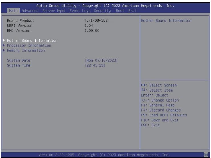

![Aptio Setup Utility - Copyright (C) 2023 American Megatrends, Inc.\nMain Advanced Server Mgmt Event Logs Security Boot Exit\nBoard Product TURINDB-2L2T\nUEFI Version 1.04\nBMC Version 1.00.00\n► Mother Board Information\n► Processor Information\n► Memory Information\nSystem Date (Mon 07/10/2023)\nSystem Time (22:41:25)\nMother Board Information\n+:-: Select Screen\n↑↓: Select Item\nEnter: Select\n+/-: Change Option\nF1: General Help\nF7: Discard Changes\nF9: Load UEFI Defaults\nF10: Save and Exit\nESC: Exit\nVersion 2.22.1285, Copyright (C) 2023 American Megatrends, Inc.](.isb-tr10-50m-13022-1000-10/8a50312ae7ea1497b7cb62bb27a634cf941a89156e40eb873c4e0fabaf82c22c.jpg)

![The image displays a simple icon of a white document page with a folded top-right corner. Faint horizontal lines are visible on the page, suggesting text. A large, bold red checkmark is overlaid diagonally across the document.](.isb-tr10-50m-13022-1000-10/16ff175c0924c4b92b98806f9d824599a7e1ddf7c34a489e1866705073639b59.jpg)
NOTE:

The illustration here is for references only. The actual layout may slightly vary depending on the model and the version used.

# 7.2.1 Motherboard Information

Press &lt;Enter&gt; to view the information of the motherboard.

<table><tr><td colspan="2">Main</td></tr><tr><td>Mother Board Information MotherBoard TURIND8-2L2T</td><td></td></tr><tr><td>BIOS Information BIOS Vendor American Megatrends Core Version 5.27 Compliancy UEFI 2.8; PI 1.7 Project Version A3084 1.04 x64 Build Date and Time 07/13/2023 19:30:42 AGESA PI Version GenoaPI-SP5 1.0.0.7 AMI RC Revision A3084 0.20 ACPI Version 64 SMBIOS Version 3.5.0 Platform Information Platform Genoa</td><td>←: Select Screen ↑↓: Select Item Enter: Select +/-: Change Option F1: General Help F7: Discard Changes F9: Load UEFI Defaults F10: Save and Exit ESC: Exit</td></tr></table>

# 7.2.2 Processor Information

Press &lt;Enter&gt; to view the information of the processor.

<table><tr><td>Main</td><td></td></tr><tr><td>Processor Information
Processor Type : AMD EPYC 9554 64-Core Processor
Processor Speed : 3118MHz
Microcode Update : A10F11/A101148
Processor Family: 19h
Processor Model: 11h
L1 Instruction Cache: 32 KB/8-way
L1 Data Cache: 32 KB/8-way
L2 Cache: 1024 KB/8-way
L3 Cache per Socket: 256 MB/16-way</td><td>←: Select Screen
↑↓: Select Item
Enter: Select
+/-: Change Option
F1: General Help
F7: Discard Changes
F9: Load UEFI Defaults
F10: Save and Exit
ESC: Exit</td></tr><tr><td colspan="2">Version 2.22.1285. Copyright (C) 2025 American Megatrends, Inc.</td></tr></table>

# 7.2.3 Memory Information

Press &lt;Enter&gt; to view the information of the memory.

<table><tr><td colspan="2">Aptio Setup Utility - Copyright (C) 2023 American Megatrends, Inc.</td></tr><tr><td>Memory Information</td><td></td></tr><tr><td>Total Memory 16 GB</td><td></td></tr><tr><td>Memory Present Number 1</td><td></td></tr><tr><td>Memory Not Present Number 7</td><td></td></tr><tr><td>DDR5_A1 DDR5-4800 16GB RDIMM</td><td></td></tr><tr><td>DDR5_B1 None</td><td></td></tr><tr><td>DDR5_C1 None</td><td></td></tr><tr><td>DDR5_E1 None</td><td></td></tr><tr><td>DDR5_G1 None</td><td></td></tr><tr><td>DDR5_H1 None</td><td></td></tr><tr><td>DDR5_I1 None</td><td></td></tr><tr><td>DDR5_K1 None</td><td></td></tr><tr><td></td><td>←: Select Screen
↑↓: Select Item
Enter: Select
+/-: Change Option
F1: General Help
F7: Discard Changes
F9: Load UEFI Defaults
F10: Save and Exit
ESC: Exit</td></tr></table>

# Advanced Screen

In this section, the user can set configurations for the following items: CPU Configuration, Chipset Configuration, Storage Configuration, NVMe Configuration, ACPI Configuration, USB Configuration, Super IO Configuration, Serial Port Console Redirection, H/W Monitor, PCI Subsystem Settings, AMD CBS, AMD PBS, PSP Firmware Versions, Network Stack Configuration, Trusted Computing, Driver Health, TLS Auth Configuration, and Instant Flash.

![Aptio Setup Utility - Copyright (C) 2023 American Megatrends, Inc.\nMain Advanced Server Mgmt Event Logs Security Boot Exit\nCPU Configuration\nChipset Configuration\nStorage Configuration\nNVMe Configuration\nACPI Configuration\nUSB Configuration\nSuper IO Configuration\nSerial Port Console Redirection\nH/W Monitor\nPCI Subsystem Settings\nAMD CBS\nAMD PBS\nPSP Firmware Versions\nNetwork Stack Configuration\nTrusted Computing\nDriver Health\nTls Auth Configuration\nIntel(R) Ethernet Controller X710 for 10GBASE-T -\n00:00:00:00:01:00\nVLAN Configuration (MAC:000000000100)\nMAC:000000000100-IPv4 Network Configuration\nMAC:000000000100-IPv6 Network Configuration\nIntel(R) Ethernet Controller X710 for 10GBASE-T -\n00:00:00:00:01:01\nVLAN Configuration (MAC:000000000101)\nMAC:000000000101-IPv4 Network Configuration\nCPU Configuration Parameters\n←→: Select Screen\n↑↓: Select Item\nEnter: Select\n+/-: Change Option\nF1: General Help\nF7: Discard Changes\nF9: Load UEFI Defaults\nF10: Save and Exit\nESC: Exit\nVersion 2.22.1285, Copyright (C) 2023 American Megatrends, Inc.](.isb-tr10-50m-13022-1000-10/2d17a14dd0265598c25407c345e9fa3b6a311e7a399650306121106e58f9f99e.jpg)

![The image displays a white document icon featuring a folded top-left corner and faint horizontal grey lines. A large, bold red checkmark is superimposed over the center of the document.](.isb-tr10-50m-13022-1000-10/970c1b6aae1d1551a6dd70a8bdedc649b4b66fafb48a8fb30797527dbea2a800.jpg)
NOTE:

Setting wrong values may cause the system to malfunction.

# 7.3.1 CPU Configuration

![Aptio Setup Utility - Copyright (C) 2023 American Megatrends, Inc.\nAdvanced\nSVM Mode	(Enabled)	Enable/disable CPU\nVirtualization\n+:-: Select Screen\n↑↓: Select Item\nEnter: Select\n+/-: Change Option\nF1: General Help\nF7: Discard Changes\nF9: Load UEFI Defaults\nF10: Save and Exit\nESC: Exit\nVersion 2.22.1285. Copyright (C) 2023 American Megatrends, Inc.](.isb-tr10-50m-13022-1000-10/63068752c56b89b3e032fcc9c2e0a42838c0fc4c805e4bae522de0fa4176f1f7.jpg)

# SVM Mode

Enable or disable CPU Virtualization.

# 7.3.2 Chipset Configuration

<table><tr><td colspan="2">Chipset Configuration Onboard VGA [Enabled] Onboard LAN (X710) [Enabled] Onboard LAN (I210-1) [Enabled] Onboard LAN (I210-2) [Enabled]</td><td>Configure Onboard VGA</td></tr><tr><td colspan="2">MCIO Mode Selection PCIE Link Width PCIE Link Speed PCIE Hotplug PCIE ASPM</td><td></td></tr><tr><td colspan="2">Onboard Debug Port LED [On]</td><td>+: Select Screen ↑↓: Select Item Enter: Select +/-: Change Option F1: General Help F7: Discard Changes F9: Load UEFI Defaults F10: Save and Exit ESC: Exit</td></tr></table>

# Onboard VGA

Use this to enable or disable the Onboard VGA function.

# Onboard LAN (X710/I210-1/I210-2)

Use this to enable or disable the Onboard LAN function.

# MCIO Mode Selection

This item is for MCIO Mode Configuration.

# MCIO3 PCIE/SATA Mode

Configure MCIO3 PCIE/SATA Mode.

# PCIE Link Width

This displays the PCIE Link Width.

# PCIE1/PCIE2/PCIE3/PCIE4/PCIE5/PCIE6 Link Width

The default values for PCIE1 and PCIE3 are [x8], others are [x16].

PCIE1/3 Link Width: x8, x4x4

PCIE2/4/5/6 Link Width: x16, x8x8, x8x4x4, x4x4x8, x4x4x4x4

# MCIO2/MCIO1 Link Width

The default values for MCIO2 and MCIO1 are [x4x4/x4x4].

# MCIO3 Link Width

The default value for MCIO3 is [x4x4].

# MCIO5/MCIO4 Link Width

The default values for MCIO5 and MCIO4 are [x4x4/x4x4].

# PCIE Link Speed

This displays the PCIE Link Speed.

# PCIE1/PCIE2/PCIE3/PCIE4/PCIE5/PCIE6 Link Speed

The default values for PCIE1/2/3/4/5/6 are [Auto].

# MCIO2/MCIO1 Link Speed

The default values for MCIO2 and MCIO1 are [Auto].

# MCIO3 Link Speed

The default value for MCIO3 is [Auto].

# MCIO5/MCIO4 Link Speed

The default values for MCIO5 and MCIO4 are [Auto].

# M2\_1/M2\_2 Link Speed

The default values for M2\_1 and M2\_2 are [Auto].

# PCIE Hotplug

Select this item to enable or disable Hot Plug for PCIE1/2/3/4/5/6/7, M2\_1/M2\_2, MCIO1/2/3/4/5 globally.

# PCIE ASPM

Select this item to disable ASPM support in all PCIe root ports. The default value is [Auto].

# Onboard Debug Port LED

Use this item to configure the onboard Dr. Debug LED.

# 7.3.3 Storage Configuration

<table><tr><td colspan="2">Aptio Setup Utility - Copyright (C) 2023 American Megatrends, Inc. Advanced</td></tr><tr><td>Storage Configuration Hard Disk S.M.A.R.T [Disabled] SATA Hot Plug [Enabled] MCI03_SATA0 : Not Detected MCI03_SATA1 : Not Detected MCI03_SATA2 : Not Detected MCI03_SATA3 : Not Detected MCI03_SATA4 : Not Detected MCI03_SATA5 : Not Detected MCI03_SATA6 : Not Detected MCI03_SATA7 : Not Detected M2_1(SATA) : Not Detected M2_2(SATA) : Not Detected</td><td>SATA Hot Plug ←: Select Screen ↑↓: Select Item Enter: Select +/-: Change Option F1: General Help F7: Discard Changes F9: Load UEFI Defaults F10: Save and Exit ESC: Exit</td></tr><tr><td colspan="2">Version 2.22.1285. Copyright (C) 2023 American Megatrends, Inc.</td></tr></table>

# Hard Disk S.M.A.R.T.

S.M.A.R.T stands for Self-Monitoring, Analysis, and Reporting Technology. It is a monitoring system for computer hard disk drives to detect and report on various indicators of reliability.

# SATA Hot Plug

Use this to enable or disable the SATA Hot Plug Function.

# 7.3.4 NVMe Configuration

<table><tr><td colspan="2">Aptio Setup Utility - Copyright (C) 2023 American Megatrends, Inc. Advanced</td></tr><tr><td rowspan="2">NVMe Configuration
Launch NVMe driver [Enabled]
No NVME Device Found</td><td>Launch NVMe driver</td></tr><tr><td>←: Select Screen
↑↓: Select Item
Enter: Select
+/-: Change Option
F1: General Help
F7: Discard Changes
F9: Load UEFI Defaults
F10: Save and Exit
ESC: Exit</td></tr><tr><td colspan="2">Version 2.22.1285. Copyright (C) 2023 American Megatrends, Inc.</td></tr></table>

The NVMe Configuration displays the NVMe controller and Drive information.

# Launch NVMe driver

Select this item to enable or disable launch NVMe driver.

# 7.3.5 ACPI Configuration

<table><tr><td colspan="2">Aptio Setup Utility - Copyright (C) 2023 American Megatrends, Inc. Advanced</td></tr><tr><td rowspan="2">ACPI Configuration
PCIE Devices Power On [Enabled]
Ring-In Power On [Disabled]
RTC Alarm Power On [By OS]</td><td>Allow the system to be waked up by a PCIE device and enable wake on LAN.</td></tr><tr><td>←: Select Screen
↑↓: Select Item
Enter: Select
+/-: Change Option
F1: General Help
F7: Discard Changes
F9: Load UEFI Defaults
F10: Save and Exit
ESC: Exit</td></tr><tr><td colspan="2">Version 2.22.1285, Copyright (C) 2023 American Megatrends, Inc.</td></tr></table>

# PCIE Devices Power On

Allows the system to be woken up by a PCIE device and enables Wake-on-LAN.

# Ring-In Power On

Allows the system to be woken up by onboard COM port modem ring-in signals.

# RTC Alarm Power On

Allows the system to be woken up by a real- time clock alarm. Set it to By OS to allow the operating system to handle this function.

# RTC Alarm Date

Use this item to set Date of RTC power on feature.

# RTC Alarm Hour

Use this item to set Hour of RTC power on feature.

# RTC Alarm Minute

Use this item to set Minute of RTC power on feature.

# RTC Alarm Second

Use this item to set Second of RTC power on feature.

# 7.3.6 USB Configuration

<table><tr><td colspan="2">Aptio Setup Utility - Copyright (C) 2023 American Megatrends, Inc. Advanced</td></tr><tr><td rowspan="2">USB Configuration
USB Controllers:
2 XHCIs
USB Devices:
1 Drive, 1 Keyboard, 1 Mouse, 5 Hubs</td><td></td></tr><tr><td>←: Select Screen
↑↓: Select Item
Enter: Select
+/-: Change Option
F1: General Help
F7: Discard Changes
F9: Load UEFI Defaults
F10: Save and Exit
ESC: Exit</td></tr><tr><td colspan="2">Version 2.22.1285. Copyright (C) 2023 American Megatrends, Inc.</td></tr></table>

This displays the USB Controllers and USB Devices information.

# 7.3.7 Super IO Configuration

![Aptio Setup Utility - Copyright (C) 2023 American Megatrends, Inc.\nAdvanced\nAST2600 Super IO Configuration\nSuper IO Chip AST2600\n► Serial Port 1 Configuration\n► SOL Configuration\nSet Parameters of COM1\n←: Select Screen\n↑↓: Select Item\nEnter: Select\n+/-: Change Option\nF1: General Help\nF7: Discard Changes\nF9: Load UEFI Defaults\nF10: Save and Exit\nESC: Exit\nVersion 2.22.1285. Copyright (C) 2023 American Megatrends, Inc.](.isb-tr10-50m-13022-1000-10/ae491f38e18a2e12c7c31207aa2e61db622a24deb0aee794a45533dd2b62cce8.jpg)

Serial Port 1 Configuration

Use this item to set parameters of Serial Port 1 (COM1).

# Serial Port

Use this item to enable or disable the serial port.

# Change Settings

Use this item to select an optimal setting for Super IO device.

# SOL Configuration

Use this item to set parameters of SOL.

# SOL Port

Use this item to enable or disable the SOL Port.

# Change Settings

Use this item to select an optimal setting for Super IO device.

# 7.3.8 Serial Port Console Redirection

<table><tr><td colspan="2">Aptio Setup Utility - Copyright (C) 2023 American Megatrends, Inc. Advanced</td></tr><tr><td>COM1
Console Redirection [Disabled]
► Console Redirection Settings</td><td rowspan="2">Console Redirection Enable or Disable.</td></tr><tr><td>SOL
Console Redirection [Disabled]
► Console Redirection Settings</td></tr><tr><td>Serial Port for Out-of-Band Management/
Windows Emergency Management Services (EMS)
Console Redirection EMS [Enabled]
► Console Redirection Settings</td><td>+: Select Screen
↑↓: Select Item
Enter: Select
+/-: Change Option
F1: General Help
F7: Discard Changes
F9: Load UEFI Defaults
F10: Save and Exit
ESC: Exit</td></tr><tr><td colspan="2">Version 2.22.1285. Copyright (C) 2023 American Megatrends, Inc.</td></tr></table>

COM1 / SOL

# Console Redirection

Use this to enable or disable Console Redirection. If this item is set to Enabled you can select a COM port to be used for Console Redirection.

# Console Redirection Settings

Use this option to configure Console Redirection settings and specify how the computer and the connected host computer exchange information. Both computers should have the same or compatible settings.

# Terminal Type

Use this to select the preferred terminal emulation type for out-of-band management.

<table><tr><td>Option</td><td>Description</td></tr><tr><td>VT100</td><td>ASCII character set</td></tr><tr><td>VT100Plus</td><td>Extended VT100 that supports color and function keys</td></tr><tr><td>VT-UTF8</td><td>UTF8 encoding is used to map Unicode chars onto 1 or more bytes</td></tr><tr><td>ANSI</td><td>Extended ASCII character set</td></tr></table>

# Bits Per Second

Use this to select the serial port transmission speed. The speed used in the host computer and the client computer must be the same. Long or noisy lines may require lower transmission speed. The options include [9600], [19200], [38400], [57600] and [115200].

# Data Bits

Use this to set the data transmission size. The options include [7] and [8] (Bits).

# Parity

Use this to select the parity bit. The options include [None], [Even], [Odd], [Mark] and [Space].

# Stop Bits

The item indicates the end of a serial data packet. The standard setting is [1] Stop Bit. Select

[2] Stop Bits for slower devices.

# Flow Control

Use this to set the flow control to prevent data loss from buffer overflow. When sending data, if the receiving buffers are full, a "stop" signal can be sent to stop the data flow. Once the buffers are empty, a "start" signal can be sent to restart the flow. Hardware flow uses two wires to send start/stop signals. The options include [None] and [Hardware RTS/CTS].

# VT-UTF8 Combo Key Support

Use this to enable or disable the VT-UTF8 Combo Key Support for ANSI/ VT100 terminals.

# Recorder Mode

Use this to enable or disable Recorder Mode to capture terminal data and send it as text messages.

# Resolution 100x31

Use this to enable or disable extended terminal resolution support.

# Putty KeyPad

Use this to select Function Key and Keypad on Putty.

# Serial Port for Out-of-Band Management/Windows Emergency Management Services (EMS)

Console Redirection EMS

Use this to enable or disable Console Redirection EMS. If this item is set to Enabled allowing to select a COM Port to be used for Console Redirection.

Console Redirection Settings

Use this to configure Console Redirection Settings, and specify how the remote computer and the host computer to which are connected exchange information. Both computers should have the same or compatible settings.

# Out-of-Band Mgmt Port

Microsoft Windows Emergency Management Services (EMS) allows for remote management of a Windows Server OS through a serial port.

# Terminal Type EMS

Use this to select the preferred terminal emulation type for out-of-band management. It is recommended to select [VT-UTF8].

<table><tr><td>Option</td><td>Description</td></tr><tr><td>VT100</td><td>ASCII character set</td></tr><tr><td>VT100+</td><td>Extended VT100 that supports color and function keys</td></tr><tr><td>VT-UTF8</td><td>UTF8 encoding is used to map Unicode chars onto 1 or more bytes</td></tr><tr><td>ANSI</td><td>Extended ASCII character set</td></tr></table>

# Bits Per Second EMS

Use this to select the serial port transmission speed. The speed used in the host computer and the client computer must be the same. Long or noisy lines may require lower transmission speed. The options include [9600], [19200], [57600] and [115200].

# Flow Control EMS

Use this to set the flow control to prevent data loss from buffer overflow. When sending data, if the receiving buffers are full, a "stop" signal can be sent to stop the data flow. Once the buffers are empty, a "start" signal can be sent to restart the flow. Hardware flow uses two wires to send start/stop signals. The options include [None], [Hardware RTS/

CTS], and [Software Xon/Xoff].

Data

Bits

Parity

Stop

Bits

# 7.3.9 H/W Monitor

It allows users to monitor the status of the hardware on the system, including the parameters of the CPU temperature, motherboard temperature, CPU fan speed, chassis fan speed, and the critical voltage.

![Aptio Setup Utility - Copyright (C) 2023 American Megatrends, Inc.\nAdvanced\nH/W Monitor\nVOLT_3.3VSB : 3.34 V\nVOLT_5VSB : 5.07 V\nVOLT_VCORE0 : 1 V\nVOLT_VCORE1 : 0.98 V\nVOLT_P0_VSOC : 1.12 V\nVOLT_VDD_11 : 1.1 V\nVOLT_VDDIO : 1.12 V\nVOLT_VDD_33 : 3.3 V\nVOLT_VDD_18 : 1.8 V\nVOLT_VCCD : 0.92 V\nVOLT_1P88V : 0.74 V\nVOLT_1POV : 1 V\nVOLT_BAT : 3.02 V\nVOLT_3V : 3.4 V\nVOLT_5V : 5.01 V\nVOLT_12V : 12 V\nFAN1 : 4000 RPM\nFAN2 : N/A\nFAN3 : N/A\nFAN4 : N/A\nFAN5 : N/A\nFAN6 : N/A\nFAN7 : N/A\n←: Select Screen\n↑↓: Select Item\nEnter: Select\n+/-: Change Option\nF1: General Help\nF7: Discard Changes\nF9: Load UEFI Defaults\nF10: Save and Exit\nESC: Exit\nVersion 2.22.1285. Copyright (C) 2023 American Megatrends, Inc.](.isb-tr10-50m-13022-1000-10/a4a101d4d0739decb03cabbbda0fde3baa1c424ba4c4d6b03edbc0bc48556c6c.jpg)

# PCI Subsystem Settings

<table><tr><td colspan="2">Aptio Setup Utility - Copyright (C) 2023 American Megatrends, Inc. Advanced</td></tr><tr><td rowspan="2">Re-Size BAR Support [Disabled] SR-IOV Support [Disabled]</td><td>If system has Resizable BAR capable PCIe Devices, this option Enables or DisablesResizable BAR Support.</td></tr><tr><td>+: Select Screen
↑↓: Select Item
Enter: Select
+/-: Change Option
F1: General Help
F7: Discard Changes
F9: Load UEFI Defaults
F10: Save and Exit
ESC: Exit</td></tr><tr><td colspan="2">Version 2.22.1285. Copyright (C) 2023 American Megatrends, Inc.</td></tr></table>

# Re-Size BAR Support

Enable or disable this item to Re-Size BAR supported upon the sysem has resizable BAR capable PCIe Devices.

# SR-IOV Support

If system has SR-IOV capable PCIe Devices, this option Enables or Disables Single Root IO Virtualization Support.

# AMD CBS

<table><tr><td colspan="2">Aptio Setup Utility - Copyright (C) 2023 American Megatrends, Inc. Advanced</td></tr><tr><td rowspan="2">AMD CBS
AMD CBS Revision Number 0x0
►CPU Common Options
►DF Common Options
►UMC Common Options
►NBIO Common Options
►FCH Common Options
►Soc Miscellaneous Control
►Workload Tuning
►CXL Common Options</td><td>CPU Common Options</td></tr><tr><td>+: Select Screen
↑↓: Select Item
Enter: Select
+/-: Change Option
F1: General Help
F7: Discard Changes
F9: Load UEFI Defaults
F10: Save and Exit
ESC: Exit</td></tr><tr><td colspan="2">Version 2.22.1285. Copyright (C) 2023 American Megatrends, Inc.</td></tr></table>

# CPU Common Options

Use this item to configure CPU Common options.

# DF Common Options

Use this item to configure DF Common options.

# UMC Common Options

Use this item to configure UMC Common options.

# NBIO Common Options

Use this item to configure NBIO Common options.

# FCH Common Options

Use this item to configure FCH Common options.

# Soc Miscellaneous Control

Use this item to configure Soc Miscellaneous Control options.

# Workload Tuning Options

Use this item to configure Workload Tuning options.

# CXL Common Options

Use this item to configure CXL Common options.

# AMD PBS

![Aptio Setup Utility - Copyright (C) 2023 American Megatrends, Inc.\nAdvanced\nAMD PBS\n► RAS\n► CXL Range Encryption\nAMD CPM RAS related settings\n+:-: Select Screen\n↑↓: Select Item\nEnter: Select\n+/-: Change Option\nF1: General Help\nF7: Discard Changes\nF9: Load UEFI Defaults\nF10: Save and Exit\nESC: Exit\nVersion 2.22.1285. Copyright (C) 2023 American Megatrends, Inc.](.isb-tr10-50m-13022-1000-10/1c0c4ff49f59db9dc60bcdfa4c20008c69ea7f7006770cf969483fb8ca7cc02f.jpg)

# RAS

Use this item to configure AMD CPM RAS related settings.

# RAS Periodic SMI Control

Use this to enable or disable Periodic SMI for polling [MCA Threshold] error.

# SMI Threshold

This limits the number of [MCA Threshold and Deferred Error SMI source] per a unit time.

# SMI Scale

Use this to define the time scale.

# SMI Scale Unit

Use this to define the unit of time scale.

# SMI Period

Use this to define the polling interval with ms unit. Input 0 value to disable this function.

# GHES Notify Type

This specifies the notification type for deferred/corrected errors.

# GHES UnCorr Notify Type

This specifies the notification type for uncorrected errors.

# PCIe GHES Notify Type

This specifies the notification type for PCIe corrected errors.

# PCIe UnCorr GHES Notify Type

This specifies the notification type for PCIe uncorrected errors.

# PCIe Root Port Corr Err Mask Reg

Use this to initialize the PCIe AER corrected error mask register of root port.

# PCIe Root Port UnCorr Err Mask Reg

Use this to initialize the PCIe AER uncorrected error mask register of root port.

# PCIe Root Port UnCorr Err Sev Reg

Use this to initialize the PCIe AER uncorrected error severity registers of root port.

# PCIe Device Corr Err Mask Reg

Use this to initialize the PCIe AER corrected error mask register of PCIe device.

# PCIe Device UnCorr Err Mask Reg

Use this to initialize the PCIe AER uncorrected error mask register of PCIe device.

# PCIe Device UnCorr Error Sev Reg

Use this to initialize the PCIe AER uncorrected error severity registers of PCIe device

# CXL DP CIE Mask Enable

Use this to enable or disable masking of CXL DP correctable error-internal error.

# DRAM Hard Post Package Repair

Use this to enable or disable the spare DRAM rows to replace malfunctioning rows via an in-field repair mechanism.

# HEST DMC Structure Support

Use this to enable or disable HEST DMC (Deferred Machine Check) structure support.

# CXL Error Report Support

Use this to enable or disable CXL error reporting.

CXL Range Encryption

Configure AMD CXL range encryption setting.

# Range 1/2/3/4/5/6/7 Memory Base

Use this item to enter memory range base address.

# Range 1/2/3/4/5/6/7 Memory Limit

Use this item to enter memory range limit address.

# Start CXL Range Encryption

Use this to encrypt all memory ranges.

# PSP Firmware Versions

<table><tr><td colspan="2">Aptio Setup Utility - Copyright (C) 2023 American Megatrends, Inc. Advanced</td></tr><tr><td>PSP Firmware Versions</td><td></td></tr><tr><td>ABL Version 10078013</td><td></td></tr><tr><td>PSP BootLoader Version 00.29.00.88</td><td></td></tr><tr><td>SMU FW Version 04.71.101.00</td><td></td></tr><tr><td>SEV FW Version 01.01.37.05</td><td></td></tr><tr><td>PHY FW Version 00.01.37.00</td><td></td></tr><tr><td>MPIO FW Version 01.00.20.3A</td><td></td></tr><tr><td>TF MPDMA FW Version 00.47.03.00</td><td></td></tr><tr><td>PM MPDMA FW Version 00.47.3A.00</td><td></td></tr><tr><td>GMI FW Version AB.01.27.00</td><td></td></tr><tr><td>RIB FW Version 02.00.08.32</td><td></td></tr><tr><td>SEC FW Version OD.0E.90.67</td><td></td></tr><tr><td>PMU FW Version 00.00.90.47</td><td></td></tr><tr><td>EMCR FW Version 00.00.E0.44</td><td></td></tr><tr><td>uCode BO Version A101020</td><td></td></tr><tr><td></td><td>←: Select Screen
↑↓: Select Item
Enter: Select
+/-: Change Option
F1: General Help
F7: Discard Changes
F9: Load UEFI Defaults
F10: Save and Exit
ESC: Exit</td></tr><tr><td>Version 2.22.1285. Copyright (C) 2023 American Megatrends, Inc.</td><td></td></tr></table>

The PSP Firmware Versions display the version information for ABL, PSP BootLoader, SMU FW, SEV FW, PHY FW, MPIO FW, TF MPDMA FW, PM MPDMA FW, GMI FW, RIB FW, SEC FW, PMU FW, EMCR FW, and uCode B0.

# Network Stack Configuration

<table><tr><td colspan="2">Aptio Setup Utility - Copyright (C) 2023 American Megatrends, Inc. Advanced</td></tr><tr><td rowspan="2">Network Stack Configuration
Network Stack [Enabled]
IPv4 PXE Support [Disabled]
IPv4 HTTP Support [Disabled]
IPv6 PXE Support [Disabled]
IPv6 HTTP Support [Disabled]
PXE boot wait time 0
Media detect count 1</td><td>Enable/Disable UEFI Network Stack</td></tr><tr><td>+:-: Select Screen
↑↓: Select Item
Enter: Select
+/-: Change Option
F1: General Help
F7: Discard Changes
F9: Load UEFI Defaults
F10: Save and Exit
ESC: Exit</td></tr><tr><td colspan="2">Version 2.22.1285. Copyright (C) 2023 American Megatrends, Inc.</td></tr></table>

# Network Stack

Use this to enable or disable UEFI Network Stack.

# IPv4 PXE Support

Use this to enable or disable IPv4 PXE boot support. If disabled, IPv4 PXE boot support will not be available.

# IPv4 HTTP Support

Use this to enable or disable IPv4 HTTP boot support. If disabled, IPv4 HTTP boot support will not be available.

# IPv6 PXE Support

Use this to enable or disable IPv6 PXE boot support. If disabled, IPv6 PXE boot support will not be available.

# IPv6 HTTP Support

Use this to enable or disable IPv6 HTTP boot support. If disabled, IPv6 HTTP boot support will not be available.

# PXE boot wait time

Wait time in seconds to press ESC key to abort the PXE boot. Use either +/- or numeric keys to set the value.

# Media detect count

Number of times the presence of media will be checked. Use either +/- or numeric keys to set the value.

# Trusted Computing

<table><tr><td colspan="2">Aptio Setup Utility - Copyright (C) 2025 American Megatrends, Inc. Advanced</td></tr><tr><td>TPM 2.0 Device Found
Firmware Version: 7.85
Vendor: IFX
Security Device Support [Enabled]
Active PCR banks SHA256
Available PCR banks SHA256
SHA256 PCR Bank [Enabled]
Pending operation [None]
Platform Hierarchy [Enabled]
Storage Hierarchy [Enabled]
Endorsement Hierarchy [Enabled]
TPM 2.0 InterfaceType [TIS]
Device Select [Auto]</td><td>Enables or Disables BIOS support for security device.
O.S. will not show Security Device. TCG EFI protocol and INT1A interface will not be available.
↔: Select Screen
↑↓: Select Item
Enter: Select
+/-: Change Option
F1: General Help
F7: Discard Changes
F9: Load UEFI Defaults
F10: Save and Exit
ESC: Exit</td></tr><tr><td colspan="2">Version 2.22.1285. Copyright (C) 2025 American Megatrends, Inc.</td></tr></table>

![The image displays an icon of a document or checklist. It features a white page with faint horizontal lines and a large red checkmark superimposed on the right side.](.isb-tr10-50m-13022-1000-10/665aaa541b949ea9c765c89e41a11f5a547a44422996b93d19a40a43864c694a.jpg)
NOTE:

Options vary depending on the version of the connected TPM module.

# Security Device Support

Enable to activate Trusted Platform Module (TPM) security for the hard disk drives.

# Active PCR banks

This item displays active PCR Banks.

# Available PCR banks

This item displays available PCR Banks.

# SHA256 PCR Bank

Use this item to enable or disable SHA256 PCR Bank

# Pending Operation

Schedule an Operation for the Security Device.

NOTE: The computer will reboot during restart in order to change State of the Device.

# Platform Hierarchy

Use this item to enable or disable Platform Hierarchy.

# Storage Hierarchy

Use this item to enable or disable Storage Hierarchy.

# Endorsement Hierarchy

Use this item to enable or disable Endorsement Hierarchy.

# TPM 2.0 InterfaceType

Select the Communication Interface to TPM 2.0 Device

# Device Select

Use this item to select the TPM device to be supported. TPM 1.2 will restrict support to TPM 1.2 devices. TPM 2.0 will restrict support to TPM 2.0 devices. Auto will support both with the default set to TPM 2.0 devices. If TPM 2.0 devices are not found, TPM 1.2 devices will be enumerated.

# 1Driver Health

![Aptio Setup Utility - Copyright (C) 2023 American Megatrends, Inc.\nAdvanced\n► Intel(R) 40GbE 4.5.05 Healthy\n► Intel(R) 40GbE 4.5.05 Healthy\nProvides Health Status for the\nDrivers/Controllers\n+: Select Screen\n↑↓: Select Item\nEnter: Select\n+/-: Change Option\nF1: General Help\nF7: Discard Changes\nF9: Load UEFI Defaults\nF10: Save and Exit\nESC: Exit](.isb-tr10-50m-13022-1000-10/0693e94a1a0697f26835adee7e383a6045707e910893db9908051201dd8389ad.jpg)

Inter (R) 40GbE 4.5.05 “ Healthy”

Provides Health Status for the Drivers/Controllers.

# Tls Auth Configuration

<table><tr><td colspan="2">Aptio Setup Utility - Copyright (C) 2023 American Megatrends, Inc.
Advanced</td></tr><tr><td rowspan="2">Server CA Configuration
Client Cert Configuration</td><td>Press &lt;Enter&gt; to configure Server CA.</td></tr><tr><td>+: Select Screen
↑↓: Select Item
Enter: Select
+/-: Change Option
F1: General Help
F7: Discard Changes
F9: Load UEFI Defaults
F10: Save and Exit
ESC: Exit</td></tr></table>

# Server CA Configuration

Press &lt;Enter&gt; to configure Server CA.

# Enroll Cert

Press &lt;Enter&gt; to enroll cert.

# Delete Cert

Press &lt;Enter&gt; to delete cert.

# Client Cert Configuration

Press &lt;Enter&gt; to configure Client Cert.

# Instant Flash

Instant Flash is a UEFI flash utility embedded in Flash ROM. This convenient UEFI update tool allows user to update system UEFI without entering operating systems first like MSDOS or Windows®. Just save the new UEFI file to the USB flash and launch this tool, then update the UEFI only in a few clicks without preparing an additional floppy diskette or other complicated flash utility. Please be noted that the USB flash drive must use FAT file system. Execute the Instant Flash utility, the utility will show the UEFI files and the respective information. Select the proper UEFI file to update UEFI, and reboot the system after the UEFI update process is completed.

# Server Mgmt

<table><tr><td colspan="3">Aptio Setup Utility - Copyright (C) 2023 American Megatrends, Inc.</td></tr><tr><td colspan="3">Main Advanced Server Mgmt Event Logs Security Boot Exit</td></tr><tr><td colspan="2">BMC Self Test Status PASSED
BMC Device ID 32
BMC Device Revision 1
BMC Firmware Revision 1.00.00
IPMI Version 2.0
IPMI BMC Interface KCS</td><td rowspan="2">Wait For BMC response for specified time out. In ASPEED2600, BMC starts at the same time when BIOS starts during AC power ON. It takes around 255 seconds to initialize Host to BMC interfaces.</td></tr><tr><td colspan="2">Wait For BMC [Enabled]
FRB-2 Timer [Disabled]
FRB-2 Timer timeout 6
FRB-2 Timer Policy [Do Nothing]
OS Watchdog Timer [Disabled]
OS Wtd Timer Timeout 10
OS Wtd Timer Policy [Reset]</td></tr><tr><td colspan="2">BMC Network Configuration
DNS Configuration
System Event Log
BMC Tools</td><td>←: Select Screen
↑↓: Select Item
Enter: Select
+/-: Change Option
F1: General Help
F7: Discard Changes
F9: Load UEFI Defaults
F10: Save and Exit
ESC: Exit</td></tr></table>

# Wait For BMC

Wait For BMC response for specified time out. BMC starts at the same time when BIOS starts during AC power ON. It takes around 255 seconds to initialize Host to BMC interfaces.

# FRB-2 Timer

Use this item to enable or disable FRB-2 timer (POST timer)

# FRB-2 Timer Timeout

Use this to define the FRB-2 Time Expiration between 1 to 30 value.

# FRB-2 Timer Policy

Configure how the system should respond. If the FRB-2 Timer expires is disabled, this item is not available.

# OS Watchdog Timer

Use this item to enable or disable OS Watchdog Timer. If enabled, starts a BIOS timer which can only be shut off by Management Software after the OS loads.

# OS Wtd Timer Timeout

Configure the OS Boot Watchdog Timer Expiration between 1 to 30 min value. If the OS Boot Watchdog Timer is disabled, this item is not available.

# OS Wtd Timer Policy

Configure how the system should respond if the OS Boot Watchdog Timer expires. If the OS Boot Watchdog Timer is disabled, this item is not available.

# BMC Network Configuration

Use this to configure BMC network parameters.

# DNS Configuration

Select this item to configure DNS parameters.

# System Event Log

Press &lt;Enter&gt; to change the SEL event log configuration.

# BMC Tools

Use this item to configure about KCS control, restore AC power loss and load BMC default settings.

# 7.4.1 BMC Network Configuration
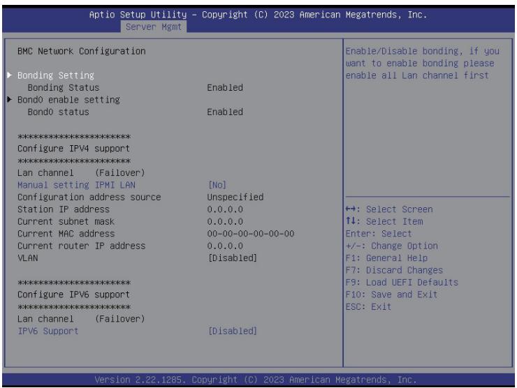
![Aptio Setup Utility - Copyright (C) 2023 American Megatrends, Inc.\nServer Mgmt\nBMC Network Configuration\n► Bonding Setting\n    Bonding Status        Enabled\n► Bond0 enable setting\n    Bond0 status        Enabled\n\n**********\nConfigure IPV4 support\n**********\nLan channel (Failover)\nManual setting IPMI LAN (No)\nConfiguration address source Unspecified\nStation IP address 0.0.0.0\nCurrent subnet mask 0.0.0.0\nCurrent MAC address 00-00-00-00-00-00\nCurrent router IP address 0.0.0.0\nVLAN (Disabled)\n\n**********\nConfigure IPV6 support\n**********\nLan channel (Failover)\nIPV6 Support (Disabled)\nEnable/Disable bonding, if you want to enable bonding please enable all Lan channel first\n←: Select Screen\n↑↓: Select Item\nEnter: Select\n+/-: Change Option\nF1: General Help\nF7: Discard Changes\nF9: Load UEFI Defaults\nF10: Save and Exit\nESC: Exit\nVersion 2.22.1285. Copyright (C) 2023 American Megatrends, Inc.](.isb-tr10-50m-13022-1000-10/e749864bd3f234d5a9983f59bd6bcffff9769c5dea7cc105b74727f0d0dd38c7.jpg)

# Bonding Setting

Select this item to enabled or disabled bonding. Please enable all LAN channel first when enabling bonding.

# Lan channel (Failover)

# Manual Setting IPMI LAN

If [No] is selected, the IP address is assigned by DHCP. If using a static IP address, toggle to [Yes], and the changes take effect after the system reboots. The default value is [No].

# Configuration Address Source

Select to configure BMC network parameters statically or dynamically (by BIOS or BMC). Configuration options: [Static] and [DHCP].

Static: Manually enter the IP Address, Subnet Mask and Gateway Address in the BIOS for BMC LAN channel configuration.

DHCP: IP address, Subnet Mask and Gateway Address are automatically assigned by the network's DHCP server.

The default login information for the IPMI web interface is:

Username: admin Password: admin

For more instructions on how to set up remote control environment and use the IPMI management platform, please refer to the IPMI Configuration User Guide.

# VLAN

Enable or disable Virtual Local Area Network.

If [Enabled] is selected, configure the items below.

VLAN ID: Select this item to configure the VLAN ID setting, the Maximum value is 4094 and the Minimum value is 1.

VLAN Priority: Select this item to configure the VLAN Priority setting. the Maximum value is 7 and the Minimum value is 0.

# IPV6 Support

Enable or disable LAN IPV6 Support.

# Manual Setting IPMI LAN(IPV6)

Select to configure LAN channel parameters statically or dynamically (by BIOS or BMC). Unspecified option will not modify any BMC network parameters during BIOS phase.

# 7.4.2 DNS Configuration

<table><tr><td>DNS Configuration Manual DNS Configuration [YES] Domain Name Service Configuration DNS Service [Enabled] Host Configuration Host Name Settings [Automatic] Host Name AMIA2429C088648 BMC Registration Settings bond Register BMC [Enabled] bond Register Method [Nupdate] Domain Name Configuration Domain Setting [bondo_v4] Domain Name Server Configuration Domain Name Server Setting [bond0] IP Priority [IPv4]</td><td>Manual DNS Configuration ↔: Select Screen ↑↓: Select Item Enter: Select +/-: Change Option F1: General Help F7: Discard Changes F9: Load UEFI Defaults F10: Save and Exit ESC: Exit</td></tr><tr><td colspan="2">Version 2.22.1285. Copyright (C) 2023 American Megatrends, Inc.</td></tr></table>

# Manual DNS Configuration

Select this item to manual configure DNS.

If [YES] is selected, configure the items below.

# DNS Service

Use this item to enable or disable DNS Service Configuration.

# Host Name Settings

Use this item to automatic or manual Host Name Settings.

# Bond Register BMC

Use this item to enable or disable Bond Register BMC.

# Bond Register Method

Use this item to configure Bond Register Method with Nsupdate or DHCP client FQDN/ Hostname..

# Domain Setting

This item supports Manual, Bond0\_v4 and Bond0\_v6 Domain Settings.

# Domain Name Server Setting

This item supports Manual and Bond0 DNS Server Settings.

# IP Priority

This item supports IPV4 and IPV6 IP Priority.

# 7.4.3 System Event Log

<table><tr><td colspan="2">Aptio Setup Utility - Copyright (C) 2023 American Megatrends, Inc.
Server Mgmt</td></tr><tr><td>Enabling/Disabling Options
SEL Components [Enabled]</td><td rowspan="4">Change this to enable or disable event logging for error/progress codes during boot.</td></tr><tr><td>Erasing Settings
Erase SEL [No]
When SEL is Full [Do Nothing]</td></tr><tr><td>Custom EFI Logging Options
Log EFI Status Codes [Error code]</td></tr><tr><td>PCIe Device Degrade ELog Support [Disabled]</td></tr><tr><td>NOTE: All values changed here do not take effect until computer is restarted.</td><td>←: Select Screen
↑↓: Select Item
Enter: Select
+/-: Change Option
F1: General Help
F7: Discard Changes
F9: Load UEFI Defaults
F10: Save and Exit
ESC: Exit</td></tr></table>

# SEL Components

Change this to enable or disable event logging for error/progress codes during boot.

# Erase SEL

Use this to choose options for erasing SEL.

# When SEL is Full

Use this to choose options for reactions to a full SEL.

# Log EFI Status Codes

Use this item to disable the logging of EFI Status Codes or log only error code or only progress code or both.

# PCIe Device Degrade ELog Support

Use this item to enable or disable PCIe Device Degrade Error Logging Support.

# 7.4.4 BMC Tools

<table><tr><td colspan="2">Aptio Setup Utility - Copyright (C) 2023 American Megatrends, Inc.
Server Mgmt</td></tr><tr><td rowspan="2">BMC Tools
KCS control [No change]
KCS control Current State Enabled
Restore AC Power Loss [No change]
Restore AC Power Current State Last State
Load BMC Default Settings</td><td>Select the KSC interface state after POST end. If [Enabled] is selected, the BMC will remain KCS interface after POST stage. If [Disabled] is selected, the BMC will disable KCS interface after POST stage</td></tr><tr><td>←: Select Screen
↑↓: Select Item
Enter: Select
+/-: Change Option
F1: General Help
F7: Discard Changes
F9: Load UEFI Defaults
F10: Save and Exit
ESC: Exit</td></tr><tr><td colspan="2">Version 2.22.1285. Copyright (C) 2023 American Megatrends, Inc.</td></tr></table>

# KCS Control

Select this KCS interface state after POST end. If [Enabled] us selected, the BMC will remain KCS interface after POST stage. If [Disabled] is selected, the BMC will disable KCS interface after POST stage

# Restore AC Power Loss

This allows user to set the power state after an unexpected AC/power loss. If [Power Off] is selected, the AC/power remains off when the power recovers. If [Power On] is selected, the AC/power resumes and the system starts to boot up when the power recovers. If [Last State] is selected, it will recover to the state before AC/power loss.

# Load BMC Default Settings

Use this item to Load BMC Default Settings

# Event Logs

![Aptio Setup Utility - Copyright (C) 2023 American Megatrends, Inc.\nMain Advanced Server Mgmt Event Logs Security Boot Exit\n► Change Smbios Event Log Settings\n► View Smbios Event Log\nPress (Enter) to change the\nSmbios Event Log configuration.\n←: Select Screen\n↑↓: Select Item\nEnter: Select\n+/-: Change Option\nF1: General Help\nF7: Discard Changes\nF9: Load UEFI Defaults\nF10: Save and Exit\nESC: Exit\nVersion 2.22.1265. Copyright (C) 2023 American Megatrends, Inc.](.isb-tr10-50m-13022-1000-10/4c82f5f31e569232f914d8f11467e01cff99ad903daaa3b543a0800a763e009e.jpg)

Change Smbios Event Log Settings

Use this item to configure the Smbios Event Log Settings.

When entering the item, the screen displays following sub-items:

# Smbios Event Log

Use this item to enable or disable all features of the SMBIOS Event Logging during system boot.

# Erase Event Log

Choose options for erasing Smbios Event Log. Erasing is done prior to any logging activation during reset.

# When Log is Full

Use this item to choose options for reactions to a full Smbios Event Log. The options include [Do Nothing] and [Erase Immediately].

# Log System Boot Event

Choose option to enable/disable logging of System boot event.

# MECI (Multiple Event Count Increment)

Use this item to enter the increment value for the multiple event counter. The valid range is from 1 to 255.

# METW (Multiple Event Time Window)

Use this item to specify the number of minutes which must pass between duplicate log entries which utilize a multiple-event counter. The value ranges from 0 to 99 minutes.

# Log EFI Status Code

Enable or disable the logging of EFI Status Codes as OEM reserved type E0 (if not already converted to legacy).

# Convert EFI Status Codes to Standard Smbios Type

Enable or disable the converting of EFI Status Codes to Standard Smbios Types (Not all may be translated).

View Smbios Event Log

Press &lt;Enter&gt; to view the Smbios Event Log records.

![The image displays a white document icon with a folded top-right corner. Faint grey horizontal lines run across the paper, suggesting text or a list. A large, bold red checkmark is overlaid on the left side of the document.](.isb-tr10-50m-13022-1000-10/101b1591d4726fe6c52db96fa7891c4b32bf6fb83e5e0b95ca920fccfdfa1958.jpg)
NOTE:

All values changed here do not take effect until the computer is restarted.

# Security

This section allows user to set or change the supervisor/user password for the system. For the user password item is allowed user to clear it.

![Aptio Setup Utility - Copyright (C) 2023 American Megatrends, Inc.\nMain Advanced Server Mgmt Event Logs Security Boot Exit\nSupervisor Password Not Installed\nUser Password Not Installed\nSupervisor Password\nUser Password\n▶ Secure Boot\nSet or change the password for\nthe administrator account.\nOnly the administrator has\nauthority to change the\nsettings in the UEFI Setup\nUtility. Leave it blank and\npress enter to remove the\npassword.\n+: Select Screen\n↑↓: Select Item\nEnter: Select\n+/-: Change Option\nF1: General Help\nF7: Discard Changes\nF9: Load UEFI Defaults\nF10: Save and Exit\nESC: Exit\nVersion 2.22.1285, Copyright (C) 2023 American Megatrends, Inc.](.isb-tr10-50m-13022-1000-10/c26daf430591a48f4e9ee87eb9e342822604427422a5db823e6b7d302f29dc52.jpg)

# Supervisor Password

Set or change the password for the administrator account. Only the administrator has authority to change the settings in the UEFI Setup Utility. Leave it blank and press enter to remove the password.

# User Password

Set or change the password for the user account. Users are unable to change the settings in the UEFI Setup Utility. Leave it blank and press enter to remove the password.

# Secure Boot

Use this to enable or disable Secure Boot Control. The default value is [Disabled]. Enable to support Windows Server 2012 R2 or later versions Secure Boot.

# Secure Boot Mode

Secure Boot mode selector: Standard/Custom. In Custom mode Secure Boot Variables can be configured without authentication.

# 7.6.1 Key Management

In this section, expert users can modify Secure Boot Policy variables without full authentication.

<table><tr><td>Vendor Keys Valid
Factory Key Provision [Disabled]
► Install default Secure Boot keys
► Clear Secure Boot keys
► Enroll Efi Image
► Export Secure Boot variables
Secure Boot variable | Size| Keys| Key Source
► Platform Key (PK)| 0| 0| No Keys
► Key Exchange Keys (KEK)| 0| 0| No Keys
► Authorized Signatures (db)| 0| 0| No Keys
► Forbidden Signatures(dbx)| 0| 0| No Keys
► Authorized TimeStamps(dbt)| 0| 0| No Keys
► OsRecovery Signatures(dbr)| 0| 0| No Keys</td><td>Install factory default Secure Boot keys after the platform reset and while the System is in Setup mode
←: Select Screen
↑↓: Select Item
Enter: Select
+/-: Change Option
F1: General Help
F7: Discard Changes
F9: Load UEFI Defaults
F10: Save and Exit
ESC: Exit</td></tr></table>

# Factory Key Provision

Install factory default Secure Boot keys after the platform reset and while the System is in Setup mode.

# Install Default Secure Boot Keys

Please install default secure boot keys if it’s the first time to use secure boot.

# Clear Secure Boot Keys

This force system to setup Mode-Clear all Secure Boot Variables. Change takes effect after reboot.

# Enroll Efi Image

Allow the image to run in Secure Boot mode. Enroll SHA256 hash of the binary into Authorized Signature Database (db).

# Export Secure Boot Variables

Copy NVRAM content of Secure Boot variables to files in a root folder on a file system de-vice.

# Platform Key (PK)

Enroll Factory Defaults or load certificates from a file:

1. Public Key Certificate in:
a) EFI\_SIGNATURE\_LIST
b) EFI\_CERT\_X509 (DER)
c) EFI\_CERT\_RSA2048 (bin)
d) EFI\_CERT\_SHAXXX
2. Authenticated UEFI Variable
3. EFI PE/COFF Image(SHA256)

Key Source: Factory, External, Mixed

# Key Exchange Keys (KEK)

Enroll Factory Defaults or load certificates from a file:

1. Public Key Certificate in:
a) EFI\_SIGNATURE\_LIST
b) EFI\_CERT\_X509 (DER)
c) EFI\_CERT\_RSA2048 (bin)
d)EFI\_CERT\_SHAXXX

2. Authenticated UEFI Variable

3. EFI PE/COFF Image(SHA256)

Key Source: Factory, External, Mixed

# Authorized Signatures (db)

Enroll Factory Defaults or load certificates from a file:

1. Public Key Certificate in:
a) EFI\_SIGNATURE\_LIST
b) EFI\_CERT\_X509 (DER)
c) EFI\_CERT\_RSA2048 (bin)
d) EFI\_CERT\_SHAXXX
2. Authenticated UEFI Variable
3. EFI PE/COFF Image(SHA256)

Key Source: Factory, External, Mixed

# Forbidden Signatures (dbx)

Enroll Factory Defaults or load certificates from a file:

1. Public Key Certificate in:
a) EFI\_SIGNATURE\_LIST
b) EFI\_CERT\_X509 (DER)
c) EFI\_CERT\_RSA2048 (bin)
d) EFI\_CERT\_SHAXXX
2. Authenticated UEFI Variable
3. EFI PE/COFF Image(SHA256)

Key Source: Factory, External, Mixed

# Authorized TimeStamps (dbt)

Enroll Factory Defaults or load certificates from a file:

1. Public Key Certificate in:
a) EFI\_SIGNATURE\_LIST
b) EFI\_CERT\_X509 (DER)
c) EFI\_CERT\_RSA2048 (bin)
d) EFI\_CERT\_SHAXXX
2. Authenticated UEFI Variable
3. EFI PE/COFF Image(SHA256)

Key Source: Factory, External, Mixed

# OsRecovery Signatures (dbr)

Enroll Factory Defaults or load certificates from a file:

1. Public Key Certificate in:
a) EFI\_SIGNATURE\_LIST
b) EFI\_CERT\_X509 (DER)
c) EFI\_CERT\_RSA2048 (bin)
d) EFI\_CERT\_SHAXXX
2. Authenticated UEFI Variable
3. EFI PE/COFF Image(SHA256)

Key Source: Factory, External, Mixed

# Boot Screen

In this section, it will display the available devices on the system for user to configure the boot settings and the boot priority.

<table><tr><td>Fixed BOOT ORDER Priorities
Boot Option #1 [Hard Disk]
Boot Option #2 [NVME]
Boot Option #3 [CD/DVD]
Boot Option #4 [USB Device]
Boot Option #5 [Network]
Boot Option #6 [UEFI AP:UEFI:
Built-in EFI Shell]</td><td>Sets the system boot order</td></tr><tr><td>UEFI Application Boot Priorities
Setup Prompt Timeout 1
Bootup Num-Lock [On]
Boot Beep [Disabled]
Full Screen Logo [Enabled]</td><td rowspan="2">+: Select Screen
↑↓: Select Item
Enter: Select
+/-: Change Option
F1: General Help
F7: Discard Changes
F9: Load UEFI Defaults
F10: Save and Exit
ESC: Exit</td></tr><tr><td>CSM(Compatibility Support Module)</td></tr></table>

# Boot Option

#1/#2/#3/#4/#5/#6 Use this to set the system boot order. UEFI

# Application Boot Priorities

Specifies the Boot Device Priority sequence from available UEFI Application.

# Setup Prompt Timeout

Configure the number of seconds to wait for the UEFI setup utility.

# Bootup Num-Lock

Select whether Num Lock should be turned on or off when the system boots up.

# Boot Beep

Select whether the Boot Beep should be turned on or off when the system boots up. Please note that a buzzer is needed.

# Full Screen Logo

Enable to display the boot logo or disable to show normal POST message.

# 7.7.1 CSM Parameters

<table><tr><td colspan="2">Aptio Setup Utility - Copyright (C) 2023 American Megatrends, Inc. Boot</td></tr><tr><td>CSM(Compatibility Support Module) [Enabled] Launch PXE OpROM Policy [Legacy only] Launch Storage OpROM Policy [Legacy only] Launch Video OpROM Policy [Legacy only]</td><td>Enable to launch the Compatibility Support Module. If you are using Windows 8 or later versions 64-bit UEFI and all of your devices support UEFI, you may also disable CSM for faster boot speed.</td></tr><tr><td></td><td>←: Select Screen ↑↓: Select Item Enter: Select +/-: Change Option F1: General Help F7: Discard Changes F9: Load UEFI Defaults F10: Save and Exit ESC: Exit</td></tr><tr><td colspan="2">Version 2.22.1285. Copyright (C) 2023 American Megatrends, Inc.</td></tr></table>

# CSM (Compatibility Support Module)

Enable to launch the Compatibility Support Module. Please do not disable unless running a WHCK test. If using Windows 8 or later versions 64-bit UEFI and all of the devices sup-port UEFI, it may also disable CSM for faster boot speed.

# Launch PXE OpROM Policy

Select UEFI only to run those that support UEFI option ROM only. Select Legacy only to run those that support legacy option ROM only. Select Do not launch to not execute both legacy and UEFI option ROM.

# Launch Storage OpROM Policy

Select UEFI only to run those that support UEFI option ROM only. Select Legacy only to run those that support legacy option ROM only. Select Do not launch to not execute both legacy and UEFI option ROM.

# Launch Video OpROM Policy

Select UEFI only to run those that support UEFI option ROM only. Select Legacy only to run those that support legacy option ROM only. Select Do not launch to not execute both legacy and UEFI option ROM.

![Aptio Setup Utility - Copyright (C) 2023 American Megatrends, Inc.\nMain Advanced Server Mgmt Event Logs Security Boot Exit\nSave Changes and Exit\nDiscard Changes and Exit\nSave Changes\nDiscard Changes\nLoad UEFI Defaults\nBoot Override\nUEFI: Built-in EFI Shell\nExit system setup after saving the changes.\nF10 key can be used for this operation.\n+:-: Select Screen\n↑↓: Select Item\nEnter: Select\n+/-: Change Option\nF1: General Help\nF7: Discard Changes\nF9: Load UEFI Defaults\nF10: Save and Exit\nESC: Exit\nVersion 2.22.1285. Copyright (C) 2023 American Megatrends, Inc.](.isb-tr10-50m-13022-1000-10/8d21175342aeb5276d3d99602fe764713abc25f2b774931d80cc165a31200ccf.jpg)

# Exit Screen

# Save Changes and Exit

When selecting this option, the following message “Save configuration changes and exit setup?” will pop-out. Press &lt;F10&gt; key or select [Yes] to save the changes and exit the UEFI SETUP UTILITY.

# Discard Changes and Exit

When selecting this option, the following message “Discard changes and exit setup?” will pop-out. Press &lt;ESC&gt; key or select [Yes] to exit the UEFI SETUP UTILITY without saving any changes.

# Save Changes

When selecting this option, the following message “Save changes?” will pop-out. Select [Yes] to save all changes.

# Discard Changes

When selecting this option, the following message “Discard changes?” will pop-out. Select [Yes] to discard all changes.

# Load UEFI Defaults

Load UEFI default values for all the setup questions. F9 key can be used for this operation.

This page intentionally left blank.

# 8 Software Support

# Install Operating System

This motherboard supports various Microsoft® Windows® Server / Linux operating systems.

# Download and Install Software Drivers

After hardware installation is completed, visit our website at https://www.adlinktech.com for drivers and other software updates

# Contact Information

For more information, contact ADLINK at https://www.adlinktech.com or reach out to your local authorized distributor.

This page intentionally left blank.

# 9 Troubleshooting

# Troubleshooting Procedures

Follow the procedures below to troubleshoot the system.

![The image displays a white document icon with a folded top-left corner. Horizontal lines run across the page. A large red checkmark is overlaid diagonally on the document.](.isb-tr10-50m-13022-1000-10/d1be218a19c9b7e8ed7bee287dbcc1ac215c927e02a4af115dd5677125a898f5.jpg)
NOTE:

Always unplug the power cord before adding, removing, or changing any hardware components. Failure to do so may cause physical injuries and damages to motherboard components.

1. Disconnect the power cable and check whether the PWR LED is off.
2. Unplug all cables, connectors and remove all add-on cards from the motherboard. Make sure that the jumpers are set to default settings.
3. Confirm that there are no short circuits between the motherboard and the chassis.
4. Install a CPU and fan on the motherboard, then connect the chassis speaker and power LED.

# If there is no power...

1. Confirm that there are no short circuits between the motherboard and the chassis.
2. Make sure that the jumpers are set to default settings.
3. Check for the correct input voltage on the power supply.
4. Verify if the battery on the motherboard provides \~3VDC. Install a new battery if necessary.

# If there is no video...

1. Try re-plugging the VGA cables and power cord.
2. Check for memory errors.

# If there are memory errors...

1. Verify that the DIMM modules are properly seated in the slots.
2. Use recommended DDR5 RDIMM/RDIMM-3DS
3. Install more than one DIMM modules that should be identical with the same brand, speed, size and chip-type.
4. Try inserting different DIMM modules into different slots to identify faulty ones.

# Unable to save system setup configurations...

1. Verify if the battery on the motherboard provides \~3VDC. Install a new battery if necessary.
2. Confirm whether the power supply provides adequate and stable power.

# Technical Support Procedures

If the problems are still unsolved, please contact ADLINK technical support via the “Ask an Expert” page: https://www.adlinktech.com/en/Askanexpert. Be sure to include the following information:

1. Contact information
2. Model name, BIOS/BMC version and problem type.
3. System configuration.
4. Problem description.

# Returning Merchandise for Service

For warranty service, the receipt or a copy of the invoice marked with the date of purchase is required. By calling the vendor or visiting ADLINK eRMA website (https://partner.adlinktech.com/AdlinkPartnerCenterWeb/User/Login) to obtain a Returned Merchandise Authorization (RMA) number.

The RMA number should be displayed on the outside of the shipping carton which is mailed prepaid or handcarried when returning the motherboard to the manufacturer. Shipping and handling charges will be applied for all orders that must be mailed when service is complete.

This warranty does not cover damages incurred in shipping or from failure due to alteration, misuse, abuse or improper maintenance of products.

Contact the distributor first for any product related problems during the warranty period.

# Safety Instructions

Read and follow all instructions marked on the product and in the documentation before you operate your system. Retain all safety and operating instructions for future use.

Please read these safety instructions carefully.
• Please keep this User‘s Manual for later reference.
• Read the specifications section of this manual for detailed information on the operating environment of this equipment.
• When installing/mounting or uninstalling/removing equipment, turn off the power and unplug any power cords/cables.
• To avoid electrical shock and/or damage to equipment:

Keep equipment away from water or liquid sources.
Keep equipment away from high heat or high humidity.
 Keep equipment properly ventilated (do not block or cover ventilation openings).
 Make sure to use recommended voltage and power source settings.
 Always install and operate equipment near an easily accessible electrical socket-outlet.
Secure the power cord (do not place any object on/over the power cord).
 Only install/attach and operate equipment on stable surfaces and/or recommended mountings.
 If the equipment will not be used for long periods of time, turn off and unplug the equipment from its power source.

• Never attempt to fix the equipment. Equipment should only be serviced by qualified personnel.

# Getting Service

Ask an Expert: https://www.adlinktech.com/en/Askanexpert

# ADLINK Technology, Inc.

Address: No. 66, Huaya 1st Road, Guishan District Taoyuan City 333, Taiwan

Tel: +886-3-216-5088

Fax: +886-3-328-5723

Email: service@adlinktech.com

# Ampro ADLINK Technology, Inc.

Address: 6450 Via Del Oro, San Jose, CA 95119-1208, USA

Tel: +1-408-360-0200

Toll Free: +1-800-966-5200 (USA only)

Fax: +1-408-600-1189

Email: info@adlinktech.com

# ADLINK Technology (China) Co., Ltd.

Address: 300 Fang Chun Rd., Zhangjiang Hi-Tech Park, Pudong New Area Shanghai, 201203 China

Tel: +86-21-5132-8988

Fax: +86-21-5132-3588

Email: market@adlinktech.com

# ADLINK Technology GmbH

Address: Hans-Thoma-Strasse 8-10, 68163 Mannheim, Germany

Tel: +49-621-43214-0

Fax: +49-621 43214-30

Email: emea@adlinktech.com

Please visit the Contact page at www.adlinktech.com for information on how to contact the ADLINK regional office nearest you.
[🔗 Link to the original document](.isb-tr10-50m-13022-1000-10/isb-tr10-50m-13022-1000-10.pdf)