# LEC-BASE 2.0

# Technical Reference

Low Energy Computer-On-Module Carrier

![Green printed circuit board with various electronic components and connectors (no visible text or labels)](.lec-base-2-0-50-1z232-1000-11/e6051cfefd20bb9970f5059cce10c866287b207954491b15e908ea93213c7742.jpg)

# Preface

# Disclaimer

Information in this document is provided in connection with ADLINK products. No license, express or implied, by estoppel or otherwise, to any intellectual property rights is granted by this document. Except as provided in ADLINK's Terms and Conditions of Sale for such products, ADLINK assumes no liability whatsoever, and ADLINK disclaims any express or implied warranty, relating to sale and/or use of ADLINK products including liability or warranties relating to fitness for a particular purpose, merchantability, or infringement of any patent, copyright or other intellectual property right. If you intend to use ADLINK products in or as medical devices, you are solely responsible for all required regulatory compliance, including, without limitation, Title 21 of the CFR (US), Directive 2007/47/EC (EU), and ISO 13485 & 14971, if any. ADLINK may make changes to specifications and product descriptions at any time, without notice.

# Trademarks

Product names mentioned herein are used for identification purposes only and may be trademarks and/or registered trademarks of their respective companies.

Revision History

<table><tr><td>Revision</td><td>Date</td><td>Description of Change(s)</td></tr><tr><td>1.1</td><td>4/19/2018</td><td>Initial Release</td></tr><tr><td></td><td></td><td></td></tr><tr><td></td><td></td><td></td></tr><tr><td></td><td></td><td></td></tr><tr><td></td><td></td><td></td></tr></table>

# © Copyright 2018 ADLINK Technology, Incorporated

www.adlinktech.com

This document contains proprietary information protected by copyright. All rights are reserved. No part of this manual may be reproduced by any mechanical, electronic, or other means in any form without prior written permission of the manufacturer.

# Audience

This manual provides reference only for computer design engineers, including but not limited to hardware and software designers and applications engineers. ADLINK Technology, Inc. assumes you are qualified to design and implement prototype computer equipment.

# Environmental Responsibility

ADLINK is committed to fulfill its social responsibility to global environmental preservation through compliance with the European Union's Restriction of Hazardous Substances (RoHS) directive and Waste Electrical and Electronic Equipment (WEEE) directive. Environmental protection is a top priority for ADLINK. We have enforced measures to ensure that our products, manufacturing processes, components, and raw materials have as little impact on the environment as possible. When products are at their end of life, our customers are encouraged to dispose of them in accordance with the product disposal and/or recovery programs prescribed by their nation or company.

# Important Safety Instructions

For user safety, please read and follow all Instructions, WARNINGS, CAUTIONS, and NOTES marked in this manual and on the associated equipment before handling/operating the equipment.

▶ Read these safety instructions carefully.
▶ Keep this manual for future reference.
▶ Read the specifications section of this manual for detailed information on the operating environment of this equipment.
▶ Turn off power and unplug any power cords/cables when installing/mounting or un-installing/removing equipment.

▶ To avoid electrical shock and/or damage to equipment:

▷ Keep equipment away from water or liquid sources;
▷ Keep equipment away from high heat or high humidity;
▷ Keep equipment properly ventilated (do not block or cover ventilation openings);
▶ Make sure to use recommended voltage and power source settings;
▶ Always install and operate equipment near an easily accessible electrical socket-outlet;
▷ Secure the power cord (do not place any object on/over the power cord);
▶ Only install/attach and operate equipment on stable surfaces and/or recommended mountings; and,
▷ If the equipment will not be used for long periods of time, turn off the power source and unplug the equipment.

# Conventions

The following conventions may be used throughout this manual, denoting special levels of information.

![The image displays a white document icon with a folded top-right corner. A large, red checkmark is centered on the document.](.lec-base-2-0-50-1z232-1000-11/da4c190f6d287b048391024218abf8617f686d026088154f9231a878c6fa6053.jpg)
NOTE:

This information adds clarity or specifics to text and illustrations.

![A yellow triangular warning sign with a black border containing a black exclamation mark in the center.](.lec-base-2-0-50-1z232-1000-11/8b6513b6477a4db8c4ad134be3e86e6da9915f278a3399b53021424caf32044a.jpg)
CAUTION:

This information indicates the possibility of minor physical injury, component damage, data loss, and/or program corruption.

![The image displays a red triangular warning sign with a black outline. Centered inside the triangle is a white exclamation point. The red fill features a gradient, appearing lighter at the top and darker at the bottom. A thin black horizontal bar is visible at the very top edge of the image.](.lec-base-2-0-50-1z232-1000-11/fa7b526d1fd48315e1a0b5dbebcee5d34e9463f081cc8b9656656cff93652fa5.jpg)
WARNING:

This information warns of possible serious physical injury, component damage, data loss, and/or program corruption.

# Table of Contents

# Preface .... ii

# 1 Product Overview .... 1

1.1 Carrier Description .... 1
1.2 Features 2
1.3 Ordering Information .... 3
1.4 Block Diagram 4
1.5 Specifications .... 5

1.5.1 Physical 5
1.5.2 Electrical 5
1.5.3 Environmental 5
1.5.4 Mechanical 6

# 2 Hardware 7

2.1 Interface Headers, Jumper Headers, Switches, LEDs, and Connectors ....7
2.2 Standard Hardware References 18

2.2.1 Audio IO Jacks 18
2.2.2 PCIe Mini Card Slot 19
2.2.3 SD Card Slot 20
2.2.4 SIM Slots 21
2.2.5 Battery Socket 22

# 3 Interfaces 23

3.1 USB Interfaces 23

3.1.1 USB11 Wake / No Wake Select (CN138) 24
3.1.2 USB12 Wake / No Wake Select (CN139) 24
3.1.3 USB4 Wake / No Wake Select (CN141) 24
3.1.4 USB2 Wake / No Wake Select (CN142) 24
3.1.5 USB5 Wake / No Wake Select (CN143) 25
3.1.6 USB0 Wake / No Wake Select (CN159) 25
3.1.7 USB3 Wake / No Wake Select (CN162) 25
3.1.8 USB4 2.0 Over-Current Detection Source Select (CN211) 25
3.1.9 USB5 2.0 Over-Current Detection Source Select (CN212) 26
3.1.10 USB3 3.0 Over-Current Detection Source Select (CN213) 26
3.1.11 USB2 3.0 Over-Current Detection Source Select (CN214) 26

3.2 Power Interfaces 27

3.2.1 ATX Power (CN2) 27
3.2.2 Battery Interface (CN111) 28
3.2.3 Battery Enable (CN110) 28
3.2.4 Smart Battery (BattMan) Interface (CN128) 28
3.2.5 BattMan SMBus Voltage Select (CN129) 29
3.2.6 BattMan Charger Interface (CN202) 29
3.2.7 BattMan Enable (CN206) 29

# 3.3 Display Interfaces 30

3.3.1 LVDS (CN25) 30
3.3.2 LVDS Backlight 0 (CN116) 31
3.3.3 LVDS Backlight 1 (CN113) 32
3.3.4 LVDS VCC Voltage Select (CN114) 32
3.3.5 LVDS VDD Voltage Select (CN117) 33
3.3.6 LVDS / eDP Mode Select (CN120) 33
3.3.7 Backlight Voltage Select (CN207) 33
3.3.8 eDP0 (CN121) 33
3.3.9 eDP1 (CN118) 35
3.3.10 HDMI (CN123) 36
3.3.11 HDMI Configuration Switch (SW46) 36
3.3.12 HDMI / DP1 Mode Select (CN125) 37
3.3.13 DisplayPort++ 0 (CN122) 37
3.3.14 DisplayPort++ 1 (CN124) 38

# 3.4 I2C Interfaces 38

3.4.1 I2C GP (CN105) 38
3.4.2 I2C CAM0 (CN106) 39
3.4.3 I2C CAM1 (CN107) 39
3.4.4 I2C PM (CN108) 39
3.4.5 I2C EEPROM Socket (CN194) 40
3.4.6 I2C\_PM Voltage Select (CN195) 40
3.4.7 I2C\_GP Voltage Select (CN196) 40
3.4.8 I2C\_CAM0 Voltage Select (CN197) 41
3.4.9 I2C\_CAM1 Voltage Select (CN198) 41

# 3.5 Fan Interface 41

3.5.1 Fan I/O (CN109) 41
3.5.2 Fan Voltage Select (CN112) 42

# 3.6 Camera Interfaces 42

3.6.1 MIPI-CSI Camera Interface (CN208) 42
3.6.2 GPIO Camera Interface (CN127) 43

# 3.7 IEEE 1588 Trigger Interface (CN130) 44

# 3.8 Serial Interfaces 44

3.8.1 COM0 (CN134 [top]) 44
3.8.2 COM1 (CN134 [bottom]) 45
3.8.3 Serial 2 (COM2) Interface (CN210) 45
3.8.4 Serial 3 (COM3) Interface (CN209) 45
3.8.5 Serial Voltage Mode Select (CN204) 46

# 3.9 CAN Interfaces (Controller Area Network) 46

3.9.1 CAN0 (CN136 [top]) 46
3.9.2 CAN0 Termination (CN137) 46
3.9.3 CAN1 (CN136 [bottom]) 47
3.9.4 CAN1 Termination (CN135) 47

# 3.10 SPI Interfaces 48

3.10.1 SPI0 Voltage Select (CN145) 48
3.10.2 SPI0 Flash Socket (CN146) 48
3.10.3 eSPI / SPI1 Voltage Select (CN147) 49
3.10.4 SPI0 Interface (CN148) 49
3.10.5 SPI0 CS0/CS1 Select (CN149) 49
3.10.6 eSPI / SPI1 Interface (CN150) 50
3.10.7 SPI0 Configuration Switch (SW51) 50
3.10.8 SPI1 Configuration Switch (SW52) 50

# 3.11 SD Card Power Mode Select (CN152) 51

# 3.12 Audio Interfaces ....51

3.12.1 HDA Voltage Select (CN154) 51
3.12.2 External / Internal Mic BIAS Select (CN156) 51
3.12.3 I2S Audio CODEC Select (CN157) 51

# 3.13 GPIO Interfaces 52

3.13.1 GPIO 0-3 Interface (CN167) 52
3.13.2 GPIO 0-3 Enable (CN163) 52
3.13.3 GPIO 0-3 Voltage Select (CN168) 52
3.13.4 GPIO 4-7 Interface (CN173) ....53
3.13.5 GPIO 4-7 Enable (CN169) ....53
3.13.6 GPIO 4-7 Voltage Select (CN174) 53
3.13.7 GPIO 8-11 Interface (CN179) ....54
3.13.8 GPIO 8-11 Enable (CN176) 54
3.13.9 GPIO 8-11 Voltage Select (CN180) 54
3.13.10 GPIO5 Fan Power Management Enable (CN199) 55
3.13.11 GPIO6 Fan Tachometer Enable (CN200) 55
3.13.12 GPIO 0-3, 2.2K PU Configuration Switch (SW68) 55
3.13.13 GPIO 4-7, 2.2K PU Configuration Switch (SW69) 56
3.13.14 GPIO 8-11, 2.2K PU Configuration Switch (SW71) 56
3.13.15 GPIO 0-3, 10K PU Configuration Switch (SW72) 56
3.13.16 GPIO 4-7, 10K PU Configuration Switch (SW73) .....57
3.13.17 GPIO 8-11, 10K PU Configuration Switch (SW74) 57

# 3.14 PCIe Interfaces ....57

3.14.1 PCIe A x1 (CN183) 57
3.14.2 PCIe D x1 (CN186) 58
3.14.3 Expansion Interface - mPCIe B (CN193) 59
3.14.4 Expansion Interface - mPCIe C (CN188) 59
3.14.5 mPCIe B/C CLKREQ Enable (CN205) 59
3.14.6 PCIe Re-Driver Socket (U174) 60

# 3.15 Miscellaneous Interfaces 61

3.15.1 SMBus ClockBuffers 0-1 Connect (CN201) 61
3.15.2 Boot Select Switch (SW39) 61
3.15.3 PLL Bandwidth Configuration Switch (SW66) 62

# Appendix A Technical Support 63

This page intentionally left blank.

# 1 Product Overview

This chapter presents a general overview of the LEC-BASE 2.0 carrier. After reviewing this chapter you should understand the following aspects of the LEC-BASE 2.0 carrier board.

▶ Carrier Description
▶ I/O Feature List
▶ Functional Block Diagram
▶ Carrier Specifications

# 1.1 Carrier Description

The ADLINK LEC-BASE 2.0 is a host carrier board for ADLINK's SMARC modules and serves as reference design for SMARC modules conforming to the SMARC 2.0 specification. The SMARC module plugs directly into the LEC-BASE 2.0 where the carrier board becomes a design platform for testing and developing your applications. Figure 1-1 provides an overview of the LEC-BASE 2.0 with call outs of its interface hardware. The proceeding sections and chapters in this manual present these features in more detail.

![ATX\neDP0\nBKLT1\neDP1\nHDMI\nDP1\nDP0\nUSB0/OTG\nCN206\nCN129\nCN110\nCN200\nCN112\nCN134\nCN142\nCN138\nCN139\nCN121\nCN137\nCN152\nSNOSER1\nCAN1\nCAN0\nCOM1\nCOM0\nSD-CARD\nUSB5\nUSB4\nUSB11\nUSB12\nDual-Channel LVDS\nDN14\nDN17\nDN207\nDKND\nSW46\nRD3\nSIM-Card\nSIM-Card\nSATA\nSMARC-Connector\nSMARC Version 2.0\nMPCle (B)\nMPCle (C)\nPCE x1 (A)\nPCE x1 (D)\nLAN, TRIQ\nLAN, LAN, LUN\nLUN, LAN, LUN, LAN, LAN, LAN, LAN, LAN, LAN, LAN, LAN, LAN, LAN, LAN, LAN, LAN, LAN, LAN, LAN, LAN, LAN, LAN, LAN, LAN, LAN, LAN, LAN, LAN, LAN, LAN, LAN, LAN, LAN, LAN, LAN, LAN, LAN, LAN, LAN, LAN, LAN, LAN, LAN, LAN, LAN, LAN, LAN, LAN, LAN, LAN, LAN, LAN, LAN, LUN, LUN, LUN, LUN, LUN, LUN, LUN, LUN, LUN, LUN, LUN, LUN, LUN, LUN, LUN, LUN, LUN, LUN, LUN, LUN, LUN, LUN, LUN, LUN, LUN, LUN, LUN, LUN, LUN, LUN, LUN, LUN, LUN, LUN](.lec-base-2-0-50-1z232-1000-11/b4dc1348e3ff1564689034d49631f33d6bfe460dc696251128b98e0af3833c1f.jpg)

Figure 1-1: LEC-BASE 2.0 IO Overview

The ADLINK LEC-BASE 2.0 supports the features of SMARC Hardware Specification version 2.0 The following section presents the list of features for the LEC-BASE 2.0.

# 1.2 Features

▶ SMARC interface MXM3 connector
▶ PCI Express Bus

▷ 2x PCIe x1 slots

▷ 2x PCIe Mini slots

▶ Serial Port UART interfaces (4x UART)

▷ Null Modem RS-232 on serial ports COM0 - COM3
▷ 2-wire and 4-wire connectors
▷ COM0 - COM3 interfaces on two 9-pin, DB9 connectors and two 10-pin headers

▶ USB interfaces

One USB 4-connector stack for ports 4-5 and 11-12 (USB 2.0)
One USB 2-connector stack for ports 2-3 (USB 3.0/2.0)
One micro-USB connector for port 0 OTG or client (USB 2.0)
▶ Two USB 2.0 ports (13-14) on the two Mini PCIe slots

▶ Gigabit Ethernet interface

▶ Two standard RJ-45 connectors (two-port stack)
Activity/Link and Speed LEDs on Ethernet connectors

▶ SDIO interface

▶ One SDIO slot, 4-bit (for SD card)

▶ Audio interfaces

▶ Supports HD Audio and AC'97
One 3-in-1 stack audio jack for I2S audio with Line In / Line Out / MIC In
One 3-in-1 stack audio jack for HD audio with Line In / Line Out / MIC In

▶ Video interfaces

▶ One standard HDMI connector for HDMI interface
▶ Two standard DisplayPort connectors (DP)
▶ Two standard embedded DisplayPort connectors (eDP)
▶ One dual-channel LVDS header (18/24-bit)
▶ Two LVDS backlight headers

▶ Power interface

▶ One ATX-2.2 Power In connector (+12V and +5V)
▷ Interface voltages are generated on the carrier (+3.3V, +1.8V, and +1.5V)
▶ Optional: BattMan power supply

▶ Camera interface

▶ One MIPI-CSI, 36-pin Flat Foil connector
▶ Two MIPI-CSI interfaces on the connector
▶ Two I $^{2}$ C camera interfaces

▶ Fan interfaces

▶ One fan power selection (12V or 5V) jumper header
▶ One fan interface header

▶ SATA interfaces

▶ One standard SATA3 connector (SATA0)
▶ One SATA Activity LED

▶ I²C interfaces
▶ One General Purpose I²C interface
▶ Two I $^{2}$ C camera interfaces
▷ One I²C Power Management interface
▶ CAN interface
▶ Two CAN DB9 connectors (stack)
▶ SPI interfaces
▶ One SPI interface header
▶ One eSPI/SPI header
▶ Miscellaneous
▶ Twelve GPIOs (interrupt capable)
▷ Watchdog LED
▷ Smart Battery Connector
▷ RTC Battery Socket
Power Button
▷ Reset Button
▷ Sleep Button
▷ Test Button
▷ LID Switch
▶ Boot Select Switch

# 1.3 Ordering Information

Table 1-1: LEC-BASE 2.0 Models

<table><tr><td>Model Number</td><td>Description</td></tr><tr><td>LEC-BASE 2.0(91-77A05-000E or higher)</td><td>SMARC evaluation carrier board for SMARC 2.0 compliant modules</td></tr></table>

# 1.4 Block Diagram

Figure 1-2 presents a functional representation of the carrier.
![**Central Block:**\n*   **SMARC 2.0 Module** (Large central vertical rectangle)\n\n**Peripheral Blocks and Connections (Right Side):**\n*   **Power**: Connected to the module via an arrow labeled **3.0V to 5.25V**.\n*   **Batman**: Connected to the module via an arrow.\n*   **USB Connections**: Six pairs of bi-directional arrows connect to the module, labeled:\n    *   **USB0 (2.0)**\n    *   **USB2 (2.0/3.0)**\n    *   **USB1 (2.0)**\n    *   **USB3 (2.0/3.0)**\n    *   **USB4 (2.0)**\n    *   **USB5 (2.0)**\n*   **Audio Connections**:\n    *   A connection labeled **I2S** connects the module to a **Codec** block. This block connects to **Line in/out, mic** via a bi-directional arrow.\n    *   A connection labeled **HDA** connects the module to a second **Codec** block. This block connects to **Line in/out, mic** via a bi-directional arrow.\n*   **Camera Connection**: A connection labeled **CSI0/1** connects the module to a **Camera Add-on Card** block.\n*   A vertical text label at the bottom right reads: **LEC-BASE 2.0_blkdiag_b**\n\n**Connections (Left Side):**\nA series of bi-directional arrows connect to the module, labeled (from top to bottom):\n*   **SD/SDIO 4-bit**\n*   **GbE0**\n*   **GbE1**\n*   **SATA (Gen1,2,3)**\n*   **SPI0 and SPI/eSPI1**\n*   **Misc**\n*   **HDMI/DP++**\n*   **SC/DC LVDS (18/24bit)/eDP0/1**\n*   **DP++**\n*   **2x PCIe x1 Gen2**\n*   **2x miniPCIe x1 Gen2**\n*   **4x UART (2x RTS/CTS)**\n*   **2x CAN**\n*   **12x GPIO**](.lec-base-2-0-50-1z232-1000-11/5c9deda290a67b83eee9d893cd80ce24b70469f3bf1c8a5eb898ed0ceb617ce5.jpg)

Figure 1-2: Functional Block Diagram

# 1.5 Specifications

# 1.5.1 Physical

Table 1-2 lists the physical dimensions of the carrier.

Table 1-2: Weight and Footprint Dimensions

<table><tr><td>Item</td><td>Dimension</td><td rowspan="6">Overall height is measured from the upper board surface to the top of the highest permanent component on the upper board surface. This measurement does not include the cooling solution, which can vary. The cooling solution will probably increase this dimension.</td></tr><tr><td>Weight</td><td>0.42 kg (0.93 lb)</td></tr><tr><td>Height (overall)</td><td>37.70 mm (1.48 inches)</td></tr><tr><td>Board thickness</td><td>2.00 mm (0.08 inches)</td></tr><tr><td>Width</td><td>170.00 mm (6.69 inches)</td></tr><tr><td>Length</td><td>304.80 mm (12.00 inches)</td></tr></table>

# 1.5.2 Electrical

Table 1-3 specifies the voltage inputs of the carrier.

Table 1-3: Carrier Voltage Inputs

<table><tr><td>Parameter</td><td>Value</td></tr><tr><td>Standard</td><td>12V +/-5% and 5V +/-5% from ATX connector</td></tr><tr><td>RTC</td><td>3.0V, 2.0V to 3.3V (battery), +/-20mV ripple</td></tr><tr><td>BattMan Supply</td><td>12V +/-5% (3A max), 5.0V +/-5% (4A max), +/-50mV ripple</td></tr></table>

# 1.5.3 Environmental

Most components on the LEC-BASE 2.0 carrier are selected as extended temperature range parts (-40°C to +85°C). Some components are not available in this temperature range. In these cases, the component temperature ranges are narrower. The LEC-BASE 2.0 is validated in the -40°C to +85°C range.

The overall system performance depends on the combination of module and carrier subsystems. Some SMARC modules are available in the industrial temperature range. Others are commercial temperature range parts. Similar considerations apply to any of the add-on cards or peripherals that are used with the LEC-BASE 2.0.

Table 1-4 defines the environmental conditions under which the carrier is qualified to operate and to be stored.

Table 1-4: Validated Temperature and Humidity Ranges

<table><tr><td>Parameter</td><td>Value</td></tr><tr><td>Temperature▶ Operating▶ Storage</td><td>▶ -40°C to +85°C▶ -55°C to +85°C</td></tr><tr><td>Humidity▶ Operating▶ Non-operating</td><td>▶ 5% to 90% relative humidity, non-condensing▶ 5% to 95% relative humidity, non-condensing</td></tr></table>

# 1.5.4 Mechanical

Figure 1-3 provides the mechanical dimensions and mounting hole sizes of the LEC-BASE 2.0. The LEC-BASE 2.0 can be mounted to a chassis using M4, B-head screws. Mezzanine cards can be mounted to the carrier using female-female standoffs with M2.5 threads and M2.5, B-head screws.
![| Dimension | Value |\n| --------- | ----- |\n| Top Left   | 170   |\n| Top Right | 165.10 |\n| Bottom Left | 10.14 |\n| Bottom Right | 98.83 |\n| Bottom Right | 10.16 |\n| Bottom Left | 7.62  |\n| Middle Left | 11.38 |\n| Middle Right | 24.18 |\n| Middle Right | 24.18 |\n| Middle Left | 298.45 |\n| Middle Right | 190.92 |\n| Bottom Right | 8xØ4.2 |\n| Bottom Left | 4xØ5.5 |\n| Bottom Right | 4xØ2.7 |\n| Bottom Left | 3xR5 |\n| Bottom Right | 3xM2.5 |\n| Bottom Right | 6x45° |\n| Bottom Left | 37    |\n| Bottom Right | 37    |\n| Bottom Right | 50.63 |\n| Bottom Left | 33.02 |\n| Middle Left | 30    |\n| Middle Right | 34    |\n| Middle Right | 30    |\n| Middle Left | 74.37 |\n| Middle Right | 95.25 |\nThe image contains a schematic diagram of the PCB layout with dimension labels and component annotations.](.lec-base-2-0-50-1z232-1000-11/56901ed74a3e105f8699021d548e46015b75148c88e84f22e2ef44d212bae90b.jpg)

![42.04\n37.7\n2\nLEC-BASE 2.0_mech_dmn_b](.lec-base-2-0-50-1z232-1000-11/1c528135fe3796aab6fd4e3ca5cbc10c8a96517093c534adba1bd95293115618.jpg)

Figure 1-3: Mechanical Dimensions (Top Side)

# 2 Hardware

This chapter describes the physical specifications of the interface connectors, headers, LEDs, and switches on the LEC-BASE 2.0. The second section of this chapter, titled Standard Hardware References, further describes the industry standard IO hardware on the carrier.

# 2.1 Interface Headers, Jumper Headers, Switches, LEDs, and Connectors

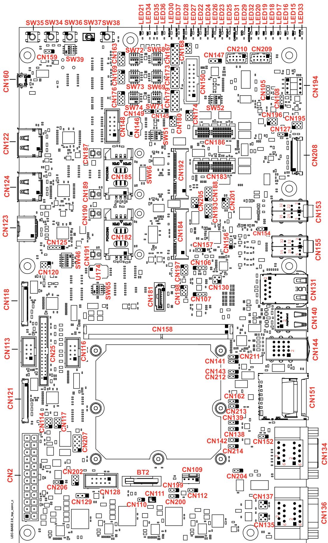
This section describes and illustrates the connectors, switches, and LEDs on the LEC-BASE 2.0. Table 2-1 lists and specifies these components, providing the PCB designator, signal name, and description of each component. Figure 2-1, Figure 2-2 (PCB designator key), Figure 2-3, and Figure 2-4 appear after Table 2-1 and illustrate the locations of these user interface components.

Table 2-1: Header, Switch, LED, and Connector Descriptions

<table><tr><td>PCB Designator</td><td>Signal / Device</td><td>Pinout Link</td><td>Description</td></tr><tr><td>BT2</td><td>Battery Socket</td><td>“Battery Socket” on page 22</td><td>3-pin socket for CR2032 batteries that run at 3V [LOTES, AAA-BAT-038-K01, BK]</td></tr><tr><td>CN2</td><td>ATX Power</td><td>Table 3-12</td><td>24-pin standard ATX power input connector [ALEX, 9359-24, NATURAL]</td></tr><tr><td>CN25</td><td>LVDS</td><td>Table 3-19</td><td>34-pin, 2.0mm header for LVDS output [JIHVEI, 23N6850-34S10B-01G-G, BLACK]</td></tr><tr><td>CN105</td><td>I2C GP</td><td>Table 3-33</td><td>4-pin, 2.0mm header for I2C general purpose signals [JIH VEI, 21N12050-04S10B-01G-4/2.8-G]</td></tr><tr><td>CN106</td><td>I2C CAM0</td><td>Table 3-34</td><td>4-pin, 2.0mm header for I2C camera 0 signals [JIH VEI, 21N12050-04S10B-01G-4/2.8-G]</td></tr><tr><td>CN107</td><td>I2C CAM1</td><td>Table 3-35</td><td>4-pin, 2.0mm header for I2C camera 1 signals [JIH VEI, 21N12050-04S10B-01G-4/2.8-G]</td></tr><tr><td>CN108</td><td>I2C PM</td><td>Table 3-36</td><td>4-pin, 2.0mm header for I2C power management signals [JIH VEI, 21N12050-04S10B-01G-4/2.8-G]</td></tr><tr><td>CN109</td><td>Fan</td><td>Table 3-42</td><td>4-pin, 2.54mm header for CPU fan signals [JVE, 24W1163-04S10-01T-02]</td></tr><tr><td>CN110</td><td>Battery Enable</td><td>Table 3-14</td><td>2-pin, 2.0mm jumper header to enable RTC coin cell battery [JIH21N12050-02S10B-01G-4/2.8-G]</td></tr><tr><td>CN111</td><td>Battery Interface</td><td>Table 3-13</td><td>2-pin, 1.25mm shrouded header for external backup battery [REGO, 830-1251-02STD-3.2-6T]</td></tr><tr><td>CN112</td><td>Fan Voltage Select</td><td>Table 3-43</td><td>3-pin, 2.0mm jumper header to select FAN supply voltage [JIH21N12050-03S10B-01G-4/2.8-G]</td></tr><tr><td>CN113</td><td>LVDS Backlight 1</td><td>Table 3-21</td><td>8-pin, 2.54mm shrouded header for LVDS backlight 1 interface [JIHVEI, 23N6960-08S10B-01G-G, BLACK]</td></tr><tr><td>CN114</td><td>LVDS +VCC Voltage Select</td><td>Table 3-22</td><td>6-pin, 2mm jumper header for selecting display +VCC LVDS voltages [JIH21N22050-06S10B-01G-4/2.8-G]</td></tr><tr><td>CN116</td><td>LVDS Backlight 0</td><td>Table 3-20</td><td>8-pin, 2.54mm shrouded header for LVDS backlight 0 interface [JIHVEI, 23N6960-08S10B-01G-G, BLACK]</td></tr><tr><td>CN117</td><td>LVDS +VDD Voltage Select</td><td>Table 3-23</td><td>6-pin, 2.0mm jumper header for selecting display +VDD LVDS voltages [JIH21N22050-06S10B-01G-4/2.8-G]</td></tr><tr><td>CN118</td><td>eDP1</td><td>Table 3-27</td><td>40-pin, 0.50mm right-angle, standard connector for embedded DisplayPort1 interface [I-PEX, 20455-040E-12]</td></tr><tr><td>CN120</td><td>LVDS / eDP Mode Select</td><td>Table 3-24</td><td>6-pin, 2.0mm jumper header for selecting between LVDS and embedded DisplayPort display modes [NELTRON, 2208SM-06G-CR]</td></tr><tr><td>CN121</td><td>eDP0</td><td>Table 3-26</td><td>40-pin, 0.50mm right-angle, standard connector for embedded DisplayPort0 interface [I-PEX, 20455-040E-12]</td></tr><tr><td>CN122</td><td>DP++0</td><td>Table 3-31</td><td>20-pin, right-angle standard connector for Dual-Mode DisplayPort 0 signals [FOXCONN, 3VD51203-D7JJ-7H, BLACK]</td></tr><tr><td>CN123</td><td>HDMI</td><td>Table 3-28</td><td>19-pin, right-angle Type A, standard connector for HDMI signals [FOXCONN, QJ51191-WED5-4F]</td></tr><tr><td>CN124</td><td>DP++1</td><td>Table 3-32</td><td>20-pin, right-angle standard connector for Dual-Mode DisplayPort 1 signals [FOXCONN, 3VD51203-D7JJ-7H, BLACK]</td></tr><tr><td>CN125</td><td>HDMI / DP1 Mode Select</td><td>Table 3-30</td><td>5-pin, 2.0mm jumper header for selecting between HDMI and DisplayPort1 display modes [SAMTEC, TMM-105-03-LM-S]</td></tr><tr><td>CN127</td><td>CAM0_GPIO / CAM1_GPIO</td><td>Table 3-45</td><td>3-pin, 2.0mm header to connect optional CAM0 and CAM1 GPIO signals [JIH21N12050-03S10B-01G-4/2.8-G]</td></tr><tr><td>CN128</td><td>BattMan</td><td>Table 3-15</td><td>10-pin, 2.54 box header for BattMan smart battery signals [JIHVEI, 23N6960-10S10B-01G-G, BLACK]</td></tr><tr><td>CN129</td><td>BattMan SMBus Voltage Select</td><td>Table 3-16</td><td>3-pin, 2.54mm jumper header for selecting voltages for the SMBus interface toward the SMART Battery. [JIH, 21N12564-03S10B-01G-6/3-G]</td></tr><tr><td>CN130</td><td>IEEE 1588 Trigger</td><td>Table 3-46</td><td>4-pin, 2.54mm header for the IEEE 1588 (Precision Time Protocol) function on the module's Ethernet controller, if supported. The signal level is always 3.3V. [JIH, 21N22564-04S10B-01G-6/3-G]</td></tr><tr><td>CN131</td><td>GbE 0 / 1 Dual Stack</td><td>See GbE Specification</td><td>16-pin standard, RJ45 connector with LEDs for Gigabit Ethernet ports 0 and 1 [UDE, RM3-168AT9VQ, BLACK]</td></tr><tr><td>CN134</td><td>COM0 [bottom] / COM1 [top]</td><td>Table 3-47</td><td>9-pin standard, stacked DB9 connectors for RS232 serial ports with 2-wire and 4-wire, RX/TX and RTS/CTS support [AMPHENOL, G17H1110131EU]</td></tr><tr><td>CN135</td><td>CAN1 Termination Select</td><td>Table 3-55</td><td>4-pin, 2.54mm jumper header for selecting CAN1 termination schemes [JIH, 21N22564-04S10B-01G-6/3-G] NOTE: Default: 120 Ohm line termination Option: 2x 60 Ohm GND centered termination</td></tr><tr><td>CN136</td><td>CAN0 [bottom] / CAN1 [top]</td><td>Table 3-52</td><td>9-pin, standard dual DB9 connectors for transmitting and receiving Controller Area Network signals [FOXCONN, DM10151-H531-4F, TEAL]</td></tr><tr><td>CN137</td><td>CAN0 Termination Select</td><td>Table 3-53</td><td>4-pin, 2.54mm jumper header for selecting CAN0 termination schemes [JIH, 21N22564-04S10B-01G-6/3-G] NOTE: Default: 120 Ohm line termination Option: 2x 60 Ohm GND centered termination</td></tr><tr><td>CN138</td><td>USB11 Wake / No Wake Select</td><td>Table 3-1</td><td>3-pin, 2.0mm jumper header to select between Wake and No Wake from sleep states for the USB11 port [JIH21N12050-03S10B-01G-4/2.8-G]</td></tr><tr><td>CN139</td><td>USB12 Wake / No Wake Select</td><td>Table 3-2</td><td>3-pin, 2.0mm jumper header to select between Wake and No Wake from sleep states for the USB12 port [JIH21N12050-03S10B-01G-4/2.8-G]</td></tr><tr><td>CN140</td><td>USB2 [bottom] / USB3 [top]</td><td>See USB 3.0 Specification</td><td>18-pin, standard dual USB 3.0 connectors for USB interface ports 2 and 3 [Amphenol, GSB3112311HR, BLUE]</td></tr><tr><td>CN141</td><td>USB4 Wake / No Wake Select</td><td>Table 3-3</td><td>3-pin, 2.0mm jumper header to select between Wake and No Wake from sleep states for the USB4 port [JIH21N12050-03S10B-01G-4/2.8-G]</td></tr><tr><td>CN142</td><td>USB2 Wake / No Wake Select</td><td>Table 3-4</td><td>3-pin, 2.0mm jumper header to select between Wake and No Wake from sleep states for the USB2 port [JIH21N12050-03S10B-01G-4/2.8-G]</td></tr><tr><td>CN143</td><td>USB5 Wake / No Wake Select</td><td>Table 3-5</td><td>3-pin, 2.0mm jumper header to select between Wake and No Wake from sleep states for the USB5 port [JIH21N12050-03S10B-01G-4/2.8-G]</td></tr><tr><td>CN144</td><td>USB 4 / 5 / 11 / 12</td><td>See USB 2.0 Specification</td><td>16-pin, standard 4-stack USB 2.0 connectors for USB interface ports 4, 5, 11, and 12 [Kuon Yi, KS-004-ATB-10-L]</td></tr><tr><td>CN145</td><td>SPI0 Voltage Select</td><td>Table 3-56</td><td>3-pin, 2.54mm jumper header for selecting SPI0 voltages [JIH, 21N12564-03S10B-01G-6/3-G]</td></tr><tr><td>CN146</td><td>SPI0 Socket</td><td>Table 3-57</td><td>8-pin, 1.27mm SPI Flash socket for SPI flash memory [LOTES, ACA-SPI-004-K01, BLACK]</td></tr><tr><td>CN147</td><td>eSPI / SPI1 Voltage Select</td><td>Table 3-58</td><td>3-pin, 2.54mm jumper header for selecting eSPI or SPI1 voltages [JIH, 21N12564-03S10B-01G-6/3-G]</td></tr><tr><td>CN148</td><td>SPI0</td><td>Table 3-59</td><td>10-pin, 2.54 box header for SPI0 interface signals [JIHVEI, 23N6960-10S10B-01G-G, BLACK]</td></tr><tr><td>CN149</td><td>SPI0 CS0 / CS1 Select</td><td>Table 3-56</td><td>3-pin, 2.0mm jumper header to select between CS0 and CS1 for the SPI0 port [JIH21N12050-03S10B-01G-4/2.8-G]</td></tr><tr><td>CN150</td><td>eSPI / SPI1</td><td>Table 3-61</td><td>16-pin, 2.54 box header for eSPI or SPI1 interface signals [JIHVEI, 23N6960-10S10B-01G-G, BLACK]</td></tr><tr><td>CN151</td><td>SD Card</td><td>Table 2-2</td><td>12-pin standard, 2.8mm slot connector for Secure Digital memory cards [TYCO, 1939115-1, BLACK]</td></tr><tr><td>CN152</td><td>SD Card Power Mode Select</td><td>Table 3-64</td><td>3-pin, 2mm jumper header to select power modes for the SD Card slot [JIH21N12050-03S10B-01G-4/2.8-G]</td></tr><tr><td>CN153</td><td>HDA</td><td>“Audio IO Jacks” on page 18</td><td>13-pin standard audio jack for three HD Audio signals: Line In (Blue), Line Out (Green), and MIC In (Pink) [FOXCONN, JA33331-HA1P-4F]</td></tr><tr><td>CN154</td><td>HDA Voltage Select</td><td>Table 3-65</td><td>3-pin, 2mm jumper header to select between 1.5 volts and 1.8 volts for the HD Audio interface [JIH21N12050-03S10B-01G-4/2.8-G]</td></tr><tr><td>CN155</td><td>I2S Audio</td><td>“Audio IO Jacks” on page 18</td><td>13-pin standard audio jack for three I2S Audio signals: Line In (Blue), Line Out (Green), and MIC In (Pink) [FOXCONN, JA33331-HA1P-4F]</td></tr><tr><td>CN156</td><td>Mic BIAS Select</td><td>Table 3-66</td><td>3-pin, 2.0mm jumper header to select between Internal and External Mic BIAS for the I2S Audio interface [JIH21N12050-03S10B-01G-4/2.8-G]</td></tr><tr><td>CN157</td><td>I2S Audio Codec Select</td><td>Table 3-67</td><td>3-pin, 2.0mm jumper header to select between SGTL5000 and TLV320 CODECs for the I2S Audio interface [JIH21N12050-03S10B-01G-4/2.8-G]</td></tr><tr><td>CN158</td><td>SMARC Interface</td><td>See SMARC 2.0 Specification</td><td>314-pin, MXM socket for receiving camera, graphics, and I/O signals from the SMARC module [FOXCONN, AS0B821-S55B-7H, BLACK]</td></tr><tr><td>CN159</td><td>USB0 Wake / No Wake Select</td><td>Table 3-6</td><td>3-pin, 2.0mm jumper header to select between Wake and No Wake from sleep states for the USB0 port [JIH21N12050-03S10B-01G-4/2.8-G]</td></tr><tr><td>CN160</td><td>USB0 OTG</td><td>See USB 2.0 Specification</td><td>5-pin standard, Type AB Micro-USB connector for USB 2.0 OTG host/device interface [HIROSE, ZX62D-AB-5P8]</td></tr><tr><td>CN162</td><td>USB3 Wake / No Wake Select</td><td>Table 3-7</td><td>3-pin, 2.0mm jumper header to select between Wake and No Wake from sleep states for the USB3 port [JIH21N12050-03S10B-01G-4/2.8-G]</td></tr><tr><td>CN163</td><td>GPIO 0-3 Enable</td><td>Table 3-69</td><td>8-pin, 2mm jumper header to enable GPIOs 0-3 [JVE, 21N22050-08M00B-01G-4-C]</td></tr><tr><td>CN167</td><td>GPIO 0-3</td><td>Table 3-68</td><td>10-pin, 2.54mm header for GPIO 0-3 signals [JIH, 21N22564-10S10B-01G-6/3-G]</td></tr><tr><td>CN168</td><td>GPIO 0-3 Voltage Select</td><td>Table 3-70</td><td>6-pin, 2.0mm jumper header for configuring the correct reference voltages for GPIO ports 0-3, otherwise connected to GND by the ESD clamping diodes. [NELTRON, 2208SM-06G-CR]</td></tr><tr><td>CN169</td><td>GPIO 4-7 Enable</td><td>Table 3-72</td><td>8-pin, 2.0mm jumper header to enable GPIOs 4-7 [JVE, 21N22050-08M00B-01G-4-C]</td></tr><tr><td>CN173</td><td>GPIO 4-7</td><td>Table 3-71</td><td>10-pin, 2.54mm header for GPIO 4-7 signals [JIH, 21N22564-10S10B-01G-6/3-G]</td></tr><tr><td>CN174</td><td>GPIO 4-7 Voltage Select</td><td>Table 3-73</td><td>6-pin, 2.0mm jumper header for configuring the correct reference voltages for GPIO ports 4-7, otherwise connected to GND by the ESD clamping diodes. [NELTRON, 2208SM-06G-CR]</td></tr><tr><td>CN176</td><td>GPIO 8-11 Enable</td><td>Table 3-75</td><td>8-pin, 2.0mm jumper header to enable GPIOs 8-11 [JVE, 21N22050-08M00B-01G-4-C]</td></tr><tr><td>CN179</td><td>GPIO 8-11</td><td>Table 3-74</td><td>10-pin, 2.54mm header for GPIO 8-11 signals [JIH, 21N22564-10S10B-01G-6/3-G]</td></tr><tr><td>CN180</td><td>GPIO 8-11 Voltage Select</td><td>Table 3-76</td><td>6-pin, 2.0mm jumper header for configuring the correct reference voltages for GPIO ports 8-11, otherwise connected to GND by the ESD clamping diodes. [NELTRON, 2208SM-06G-CR]</td></tr><tr><td>CN181</td><td>SATA0</td><td>See SATA Specification</td><td>7-pin, 1.27mm standard vertical connector for SATA0 interface [MOLEX, 67800-5005, BLACK]</td></tr><tr><td>CN182</td><td>SIM1</td><td>“SIM Slots” on page 21</td><td>6-pin, 2.54mm standard slot, hinge connector for Subscriber Identity Module 1 interface [REGO, 80440GFH-061-128L, BLACK]</td></tr><tr><td>CN183</td><td>PCIe A</td><td>Table 3-85</td><td>36-pin, 1.0mm standard connector for PCI Express x1, Port A [FOXCONN, 2EG01827-D2D-DF]</td></tr><tr><td>CN184</td><td>mPCIe B</td><td>“PCIe Mini Card Slot” on page 19</td><td>52-pin, 0.8mm standard, right-angle slot for PCI Express Mini Card B interface [Attend, 119A-80A00-R02]</td></tr><tr><td>CN185</td><td>SIM2</td><td>“SIM Slots” on page 21</td><td>6-pin, 2.54mm standard slot, hinge connector for Subscriber Identity Module 2 interface [REGO, 80440GFH-061-128L, BLACK]</td></tr><tr><td>CN186</td><td>PCIe D</td><td>Table 3-86</td><td>36-pin, 1.0mm standard connector for PCI Express x1, Port D [FOXCONN, 2EG01827-D2D-DF]</td></tr><tr><td>CN187</td><td>mPCIe B Latch</td><td>Not Applicable</td><td>Latch for fastening PCI Express Mini Card B [Attend, 119A-LATCH-80]</td></tr><tr><td>CN188</td><td>mPCIe C Expansion</td><td>Table 3-88</td><td>8-pin, 2mm header to expand PCI Express Mini Card C interface [JVE, 21N22050-08M00B-01G-4-C]</td></tr><tr><td>CN189</td><td>mPCIe B Latch</td><td>Not Applicable</td><td>Latch for fastening PCI Express Mini Card B [Attend, 119A-LATCH-80]</td></tr><tr><td>CN190</td><td>mPCIe C Latch</td><td>Not Applicable</td><td>Latch for fastening PCI Express Mini Card C [Attend, 119A-LATCH-80]</td></tr><tr><td>CN191</td><td>mPCIe C Latch</td><td>Not Applicable</td><td>Latch for fastening PCI Express Mini Card C [Attend, 119A-LATCH-80]</td></tr><tr><td>CN192</td><td>mPCIe C</td><td>“PCIe Mini Card Slot” on page 19</td><td>52-pin, 0.8mm standard, right-angle slot for PCI Express Mini Card C interface [Attend, 119A-80A00-R02]</td></tr><tr><td>CN193</td><td>mPCIe B Expansion</td><td>Table 3-87</td><td>8-pin, 2.0mm header to expand PCI Express Mini Card B interface [JVE, 21N22050-08M00B-01G-4-C]</td></tr><tr><td>CN194</td><td>I2C EEPROM Socket</td><td>Table 3-37</td><td>8-pin, 2.54mm socket for I2C EEPROM [Mill-Max, 110-13-308-41-001000]</td></tr><tr><td>CN195</td><td>I2C PM Voltage Select</td><td>Table 3-38</td><td>6-pin, 2.0mm jumper header for selecting between 1.8V, 5.0V, and 3.3V voltages for the I2C Power Management interface [NELTRON, 2208SM-06G-CR]</td></tr><tr><td>CN196</td><td>I2C GP Voltage Select</td><td>Table 3-39</td><td>6-pin, 2.0mm jumper header for selecting between 1.8V, 5.0V, and 3.3V voltages for the I2C General Purpose interface [NELTRON, 2208SM-06G-CR]</td></tr><tr><td>CN197</td><td>I2C CAM0 Voltage Select</td><td>Table 3-40</td><td>6-pin, 2.0mm jumper header for selecting between 1.8V, 5.0V, and 3.3V voltages for the I2C CAM0 interface [NELTRON, 2208SM-06G-CR]</td></tr><tr><td>CN198</td><td>I2C CAM1 Voltage Select</td><td>Table 3-41</td><td>6-pin, 2.0mm jumper header for selecting between 1.8V, 5.0V, and 3.3V voltages for the I2C CAM1 interface [NELTRON, 2208SM-06G-CR]</td></tr><tr><td>CN199</td><td>GPIO5 Fan PM Out Enable</td><td>Table 3-77</td><td>3-pin, 2.0mm jumper header to enable Fan Power Management Out on the GPIO5 port [JIH21N12050-03S10B-01G-4/2.8-G]</td></tr><tr><td>CN200</td><td>GPIO6 TACHO In Enable</td><td>Table 3-78</td><td>3-pin, 2.0mm jumper header to enable Tachometer In on the GPIO6 port [JIH21N12050-03S10B-01G-4/2.8-G]</td></tr><tr><td>CN201</td><td>PCIe ClockBuffers 0-1 Connect</td><td>Table 3-91</td><td>6-pin, 2.0mm jumper header for connecting one of the two PCIe ClockBuffers (0 or 1) to the SMBus [NELTRON, 2208SM-06G-CR]</td></tr><tr><td>CN202</td><td>BattMan Charger</td><td>Table 3-17</td><td>6-pin, 2.0mm header for Smart Battery charger interface [NELTRON, 2208SM-06G-CR]</td></tr><tr><td>CN204</td><td>Serial Voltage Mode Select</td><td>Table 3-51</td><td>3-pin, 2mm jumper header to select between +V1P8S and +V1P8_SBY for the Serial interface [JIH21N12050-03S10B-01G-4/2.8-G]</td></tr><tr><td>CN205</td><td>mPCIe B/C CLKREQ Enable</td><td>Table 3-89</td><td>6-pin, 2.0mm header to enable mPCIe B or C request for clock [NELTRON, 2208SM-06G-CR]</td></tr><tr><td>CN206</td><td>BattMan Enable</td><td>Table 3-18</td><td>3-pin, 2mm jumper header to enable the BattMan smart battery interface [JIH21N12050-03S10B-01G-4/2.8-G]</td></tr><tr><td>CN207</td><td>Backlight Voltage Select</td><td>Table 3-25</td><td>8-pin, 2.54mm jumper header to select between 12V and 5V for the LVDS / eDP Backlight interface [JIH, 21N22564-08S10B-01G-6/3-G]</td></tr><tr><td>CN208</td><td>MIPI-CSI Camera</td><td>Table 3-44</td><td>36-pin, 0.5mm FFC/FPC connector for the MIPI-CSI camera interface with SGET pinout [HIROSE, FH12A-36S-0.5SH(55)]</td></tr><tr><td>CN209</td><td>COM3</td><td>Table 3-50</td><td>10-pin, 2.0mm box header for serial port 3 interface signals [MOLEX, 87832-1014, BLACK]</td></tr><tr><td>CN210</td><td>COM2</td><td>Table 3-49</td><td>10-pin, 2.0mm box header for serial port 2 interface signals [MOLEX, 87832-1014, BLACK]</td></tr><tr><td>CN211</td><td>USB4 2.0 (CN144) Over-Current Detection Source Select</td><td>Table 3-8</td><td>3-pin, 2.0mm jumper header to select the source for USB4 2.0 over-current detection [JIH21N12050-03S10B-01G-4/2.8-G]</td></tr><tr><td>CN212</td><td>USB5 2.0 (CN144) Over-Current Detection Select</td><td>Table 3-9</td><td>3-pin, 2.0mm jumper header to select the source for USB5 2.0 over-current detection [JIH21N12050-03S10B-01G-4/2.8-G]</td></tr><tr><td>CN213</td><td>USB3 3.0 (CN140) Over-Current Detection Select</td><td>Table 3-10</td><td>3-pin, 2.0mm jumper header to select the source for USB3 3.0 over-current detection [JIH21N12050-03S10B-01G-4/2.8-G]</td></tr><tr><td>CN214</td><td>USB2 3.0 (CN140) Over-Current Detection Select</td><td>Table 3-11</td><td>3-pin, 2.0mm jumper header to select the source for USB2 3.0 over-current detection [JIH21N12050-03S10B-01G-4/2.8-G]</td></tr><tr><td>LED15</td><td>USB12, VBUS On</td><td>Table 3-8</td><td>Green LED indicating Vbus is applied to USB12 [LIGITEK, LG-192G-CT]</td></tr><tr><td>LED16</td><td>USB4, VBUS On</td><td>Not Applicable</td><td>Green LED indicating Vbus is applied to USB4 [LIGITEK, LG-192G-CT]</td></tr><tr><td>LED17</td><td>USB11, VBUS On</td><td>Not Applicable</td><td>Green LED indicating Vbus is applied to USB11 [LIGITEK, LG-192G-CT]</td></tr><tr><td>LED18</td><td>USB5, VBUS On</td><td>Not Applicable</td><td>Green LED indicating Vbus is applied to USB5 [LIGITEK, LG-192G-CT]</td></tr><tr><td>LED19</td><td>USB2, VBUS On</td><td>Not Applicable</td><td>Green LED indicating Vbus is applied to USB2 [LIGITEK, LG-192G-CT]</td></tr><tr><td>LED20</td><td>USB3, VBUS On</td><td>Not Applicable</td><td>Green LED indicating Vbus is applied to USB3 [LIGITEK, LG-192G-CT]</td></tr><tr><td>LED21</td><td>USB0, VBUS On</td><td>Not Applicable</td><td>Green LED indicating Vbus is applied to USB0 [LIGITEK, LG-192G-CT]</td></tr><tr><td>LED22</td><td>WLANB</td><td>Not Applicable</td><td>Green LED indicating wireless LAN connection on PCIe B [LIGITEK, LG-192G-CT]</td></tr><tr><td>LED23</td><td>WLANC</td><td>Not Applicable</td><td>Green LED indicating wireless LAN connection on PCIe C [LIGITEK, LG-192G-CT]</td></tr><tr><td>LED24</td><td>WPANB</td><td>Not Applicable</td><td>Green LED indicating wireless PAN (Bluetooth, Zigbee, or similar) connection on PCIe B [LIGITEK, LG-192G-CT]</td></tr><tr><td>LED25</td><td>WPANC</td><td>Not Applicable</td><td>Green LED indicating wireless PAN (Bluetooth, Zigbee, or similar) connection on PCIe C [LIGITEK, LG-192G-CT]</td></tr><tr><td>LED26</td><td>WWANC</td><td>Not Applicable</td><td>Green LED indicating wireless WAN (GSM, LTE, or similar) connection on PCIe C [LIGITEK, LG-192G-CT]</td></tr><tr><td>LED27</td><td>WWANB</td><td>Not Applicable</td><td>Green LED indicating wireless WAN (GSM, LTE, or similar) connection on PCIe B [LIGITEK, LG-192G-CT]</td></tr><tr><td>LED28</td><td>ALL DONE</td><td>Not Applicable</td><td>Green LED indicating when load for PCIe repeater EEPROM is complete (currently not used) [LIGITEK, LG-192G-CT]</td></tr><tr><td>LED29</td><td>SATA</td><td>Not Applicable</td><td>Yellow LED indicating SATA activity [EVERLIGHT, 19-21UYC/S350-A3/TR8]</td></tr><tr><td>LED30</td><td>BattMan Low</td><td>Not Applicable</td><td>Red LED indicating insufficient capacity of BattMan smart battery [LIGITEK, LG-192HRF-CT]</td></tr><tr><td>LED31</td><td>Power, Carrier</td><td>Not Applicable</td><td>Green LED indicating applied power to carrier [LIGITEK, LG-192G-CT]</td></tr><tr><td>LED32</td><td>Power, Module</td><td>Not Applicable</td><td>Green LED indicating applied power to module [LIGITEK, LG-192G-CT]</td></tr><tr><td>LED33</td><td>Power, SD Card</td><td>Not Applicable</td><td>Green LED indicating applied power to SD card [LIGITEK, LG-192G-CT]</td></tr><tr><td>LED34</td><td>WDT Time Out</td><td>Not Applicable</td><td>Red LED indicating a watchdog event from the module [LIGITEK, LG-192HRF-CT]</td></tr><tr><td>LED35</td><td>Carrier Standby (S3)</td><td>Not Applicable</td><td>Green LED indicating the Standby mode is active on the module (x86) [LIGITEK, LG-192G-CT]</td></tr><tr><td>LED36</td><td>BattMan Charging</td><td>Not Applicable</td><td>Yellow LED indicating BattMan smart battery is charging [EVERLIGHT, 19-21UYC/S350-A3/TR8]</td></tr><tr><td>LED37</td><td>BattMan Charger Present</td><td>Not Applicable</td><td>Green LED indicating BattMan charger is connected [LIGITEK, LG-192G-CT]</td></tr><tr><td>SW34</td><td>Power On, module</td><td>Not Applicable</td><td>Push-button switch to Power On or shut down the module [CONTACT, TS-A02-2, BLACK]</td></tr><tr><td>SW35</td><td>Reset, module</td><td>Not Applicable</td><td>Push-button switch to warm reset the module [CONTACT, TS-A02-2, BLACK]</td></tr><tr><td>SW36</td><td>Sleep, module</td><td>Not Applicable</td><td>Push-button switch to induce module sleep mode [CONTACT, TS-A02-2, BLACK]</td></tr><tr><td>SW37</td><td>LID</td><td>Not Applicable</td><td>Toggle switch to assert LID function on module [NKK, G12AP, BLACK]</td></tr><tr><td>SW38</td><td>Test</td><td>Not Applicable</td><td>Push-button switch to invoke test on the module [CONTACT, TS-A02-2, BLACK]NOTE: Supported only on LEC-iMX6</td></tr><tr><td>SW39</td><td>Boot Select</td><td>Table 3-92</td><td>4-pole, 1.27mm dip switch to select order of boot for devices on module and carrier [DIPTRONICS] DHA-04TQR, BLACK]</td></tr><tr><td>SW46</td><td>HDMI Configuration</td><td>Table 3-29</td><td>4-pole, 1.27mm dip switch to HDMI extender function [DIPTRONICS] DHA-04TQR, BLACK]</td></tr><tr><td>SW51</td><td>SPI0 Configuration</td><td>Table 3-62</td><td>4-pole, 1.27mm dip switch to configure the SPI0 socket [DIPTRONICS] DHA-04TQR, BLACK]</td></tr><tr><td>SW52</td><td>SPI1 Configuration</td><td>Table 3-63</td><td>4-pole, 1.27mm dip switch to configure the SPI1 interface [DIPTRONICS] DHA-04TQR, BLACK]</td></tr><tr><td>SW66</td><td>PLL Bandwidth Configuration</td><td>Table 3-94</td><td>2-pole, 1.6mm dip switch to configure PLL bandwidth for PCIe Clock-Buffer components [DIPTRONIC, DHNF-02-TV-T/6, HALF]</td></tr><tr><td>SW68</td><td>GPIO 0-3 Configuration</td><td>Table 3-79</td><td>4-pole, 1.27mm dip switch to configure the 2.2K pull up of GPIO ports 0-3 (carrier side) [DIPTRONICS] DHA-04TQR, BLACK]</td></tr><tr><td>SW69</td><td>GPIO 4-7 Configuration</td><td>Table 3-80</td><td>4-pole, 1.27mm dip switch to configure the 2.2K pull up of GPIO ports 4-7 (carrier side) [DIPTRONICS] DHA-04TQR, BLACK]</td></tr><tr><td>SW71</td><td>GPIO 8-11 Configuration</td><td>Table 3-81</td><td>4-pole, 1.27mm dip switch to configure the 2.2K pull up of GPIO ports 8-11 (carrier side) [DIPTRONICS] DHA-04TQR, BLACK]</td></tr><tr><td>SW72</td><td>GPIO 0-3 Configuration</td><td>Table 3-82</td><td>4-pole, 1.27mm dip switch to configure the 10K pull up of GPIO ports 0-3 (module side) [DIPTRONICS] DHA-04TQR, BLACK]</td></tr><tr><td>SW73</td><td>GPIO 4-7 Configuration</td><td>Table 3-83</td><td>4-pole, 1.27mm dip switch to configure the 10K pull up of GPIO ports 4-7 (module side) [DIPTRONICS] DHA-04TQR, BLACK]</td></tr><tr><td>SW74</td><td>GPIO 8-11 Configuration</td><td>Table 3-84</td><td>4-pole, 1.27mm dip switch to configure the 10K pull up of GPIO ports 8-11 (module side) [DIPTRONICS] DHA-04TQR, BLACK]</td></tr><tr><td>U174</td><td>PCIe Re-driver socket</td><td>Table 3-90</td><td>8-pin, 1.27mm socket for the I2C EEPROM [LOTES, ACA-SPI-004-K01, BLACK]NOTE: This socket is the same part as the SPI Flash socket but supports only the I2C EEPROM, not the SPI flash</td></tr></table>

![LEC-BASE 2.0_top_conn.c\nCN2\nCN121\nCN113\nCN118\nCN123\nCN124\nCN122\nCN160\nCN206\nCN202\nCN117\nCN25\nCN120\nCN125\nSW46\nCN191\nCN190\nCN189\nCN187\nU174\nSW65\nFOXCONN\nCN182\nFOXCONN\nCN185\nCN148\nCN149\nCN176\nCN169\nCN163\nSW72\nSW39\nSW35 SW34 SW36 SW37 SW38\nLED21\nLED34\nLED35\nLED36\nLED30\nLED37\nLED28\nLED27\nLED22\nLED24\nLED26\nLED23\nLED25\nLED31\nLED29\nLED32\nLED20\nLED19\nLED18\nLED17\nLED16\nLED15\nLED33\nCN136\nCN134\nCN151\nCN144\nCN140\nCN131\nCN155\nCN153\nCN208\nCN194\nCN204\nCN158\nCN143\nCN212\nCN162\nCN211\nCN154\nCN54\nCN53\nCN52\nCN205\nCN193 CN188 CN201 CN156 CN201 CN157 CN156 CN205 CN198 CN197 CN184 CN192 CN174 CN150 CN147 CN209 CN105 CN108 CN106 CN207 CN199 CN198 CN206 CN197 CN204 CN203 CN196 CN203 CN202 CN199 CN198 CN202 CN201 CN198 CN200 CN197 CN200 CN196 CN200 CN195 CN207 CN206 CN205 CN204 CN203 CN202 CN201 CN199 CN200 CN200 CN200 CN200 CN200 CN200 CN200 CN200 CN200 CN200 CN200 CN200 CN200 CN200 CN200 CN200 CN200 CN200 CN200 CN200 CN200 CN200 CN200 CN200 CN200 CN20(nl)](.lec-base-2-0-50-1z232-1000-11/5ef1070ad5f414c1c1a0cb0a13e80cd4d7a0bc8288e9211c45d1baa14088538a.jpg)

Figure 2-1: Header, Connector, Switch, and LED Locations (Top Side)

# CONNECTORS:

BT2 - Battery Socket

CN2 - ATX Power Input

CN25 - LVDS, Dual-Channel Interface

CN105 - I2C\_GP Interface

CN106 - I2C CAM0 Interface

CN107 - I2C CAM1 Interface

CN108 - I2C\_PM Interface

CN109 - Fan Interface

CN110 - RTC Battery Enable

CN111 - RTC Battery Interface

CN112 - Fan Voltage Select

CN113 - LVDS Backlight 1 Interface

CN114 - LVDS +VCC Voltage Select

CN116 - LVDS Backlight 2 Interface

CN117 - LVDS +VDD Voltage Select

CN118 - eDP1 Interface

CN120 - LVDS\_eDP Select

CN121 - eDP0 Interface

CN122 - DP0 Interface

CN123 - HDMI Interface

CN124 - DP1 Interface

CN125 - HDMI DP1 Select

CN127 - CAM0\_GPIO/CAM1\_GPIO Select

CN128 - BattMan Interface

CN129 - BattMan Voltage Select

CN130 - Gb Ethernet-TRIGGER Select

CN131 - Gb Ethernet Stack

CN134 - COM0/COM1 Stack

CN135 - CAN1 Termination Select

CN136 - CAN0/CAN1 Stack

CN137 - CAN0 Termination Select

CN138 - USB11 Wake/NoWake Select

CN139 - USB12 Wake/NoWake Select

CN140 - USB 3.0 Stack (ports 2/3)

CN141 - USB4 Wake/NoWake Select

CN142 - USB2 Wake/NoWake Select

CN143 - USB5 Wake/NoWake Select

CN144 - USB 2.0 Stack
 ports 4/5 and 11/12)

CN145 - SPI0 Voltage Select

CN146 - SPI0 Socket

CN147 - eSPI\_SPI1 Voltage Select

CN148 - SPI0 Interface

CN149 - SPI0 CS0/CS1 Select

CN150 - eSPI\_SPI1 Interface

CN151 - SD-Card Slot

CN152 - SD-Card Power Mode Select

CN153 - HD Audio Stack

CN154 - HD Audio Voltage Select

CN155 - I2S Audio Stack

CN156 - External/Internal Mic Bias select

CN157 - I2S Audio CODEC select

CN158 - SMARC Interface

CN159 - USB0 Wake/NoWake Select

CN160 - USB0 2.0 OTG Interface

CN162 - USB3 Wake/NoWake Select

CN163 - GPIO 0-3 Enable

CN167 - GPIO 0-3 Interface

CN168 - GPIO 0-3 Voltage Select

CN169 - GPIO 4-7 Enable

CN173 - GPIO 4-7 Interface

CN174 - GPIO 4-7 Voltage Select

CN176 - GPIO 8-11 Enable

CN179 - GPIO 8-11 Interface

CN180 - GPIO 8-11 Voltage Select

CN181 - SATA0

CN182 - SIM1 Card Interface

CN183 - PCIe A Interface

CN184 - mPCIe B Interface

CN185 - SIM2 Card Interface

CN186 - PCIe D Interface

CN187 - mPCIe B Latch

CN188 - Expansion Interface (mPCIe C)

CN189 - mPCIe B Latch

CN190 - mPCIe C Latch

CN191 - mPCIe C Latch

CN192 - mPCIe C Interface

CN193 - Expansion Interface (mPCIe B)

CN194 - I2C EEPROM Socket

CN195 - I2C\_PM Voltage Select

CN196 - I2C GP Voltage Select

CN197 - I2C-CAM0 Voltage Select

CN198 - I2C-CAM1 Voltage Select

CN199 - GPIO5 Fan PWM\_OUT Enable

CN200 - GPIO6 Fan TACHO IN Enable

CN201 - PCIe ClockBuffers 0-1 Connect

CN202 - BattMan Charger Interface

CN204 - Serial Voltage Mode Select

CN205 - mPCIe B/C CLKREQ Enable

CN206 - BattMan Enable

CN207 - Backlight Voltage Select

CN208 - MIPI-CSI Camera Interface

CN209 - COM3 Interface

CN210 - COM2 Interface

CN211 - USB4 2.0 Over-Current Detection Source Select

CN212 - USB5 2.0 Over-Current Detection Source Select

CN213 - USB3 3.0 Over-Current Detection Source Select

CN214 - USB2 3.0 Over-Current Detection Source Select

U174 - PCIe Redriver Socket

# LEDs:

LED15 - USB12, VBUS\_ON

LED16 - USB4, VBUS ON

LED17 - USB11, VBUS\_ON

LED18 - USB5, VBUS\_ON

LED19 - USB2, VBUS ON

LED20 - USB3, VBUS ON

LED21 - USB0, VBUS\_ON

LED22 - WLANB

LED23 - WLANC

LED24 - WPANB

LED25 - WPANC

LED26 - WWANC

LED27 - WWANB

LED28 - ALL DONE, PCIe

LED29 - SATA Activity

LED30 - BattMan Low

LED31 - Carrier Power

LED32 - Module Power

LED33 - SD Card Power

LED34 - WDT Time Out

LED35 - Carrier Standby (S3)

LED36 - BattMan Charging

LED37 - BattMan Charger Present

# SWITCHES:

SW34 - Button,

Power On SMARC Module

SW35 - Button,

Reset SMARC Module

SW36 - Button,

Sleep Mode SMARC Module

SW37 - Toggle, LID

SW38 - Button, Test

SW39 - Dip Switch,

Boot Select

SW46 - Dip Switch,

HDMI Configuration

SW51 - Dip Switch,

SPI0 Configuration

SW52 - Dip Switch,

SPI1 Configuration

SW66 - Dip Switch,

PLL Bandwidth Configuration

SW68 - Dip Switch,

GPIO 0-3 2.2K PU Configuration

SW69 - Dip Switch,

GPIO 4-7 2.2K PU Configuration

SW71 - Dip Switch,

GPIO 8-11 2.2K PU Configuration

SW72 - Dip Switch,

GPIO 0-3 10K PU Configuration

SW73 - Dip Switch,

GPIO 4-7 10K PU Configuration

SW74 - Dip Switch,

GPIO 8-11 10K PU Configuration

Figure 2-2: PCB Designator Key for Headers, Connectors, Switches, and LEDs

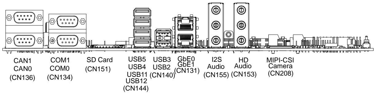
Figure 2-3 illustrates the faces of the standard interface connectors mounted along one edge of the carrier. These connectors are for CAN, Serial Port, SD Card, USB, Ethernet, Audio, and MIPI-CSI Camera (conforming to the QSeven 2.1 Specification) cable connectors.
![CAN1\nCAN0\n(CN136)\nCOM1\nCOM0\n(CN134)\nSD Card\n(CN151)\nUSB5\nUSB4\nUSB11\nUSB12\n(CN144)\nUSB3\nUSB2\n(CN140)\nGbE0\nGbE1\n(CN131)\nI2S\nAudio\n(CN155)\nHD\nAudio\n(CN153)\nMIPI-CSI\nCamera\n(CN208)](.lec-base-2-0-50-1z232-1000-11/b01ee030f3f605a0f0ce13c8d116e0341769b4f4fd26f126caa78b2271290e21.jpg)

Figure 2-3: IO Panel Connector Locations

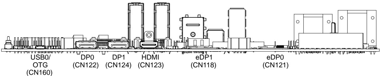
Figure 2-4 illustrates the faces of the standard interface connectors mounted along the opposite edge of the carrier shown in Figure 2-3. These connectors are for USB / OTG, DisplayPort, HDMI, and embedded DisplayPort industry-standard cable connectors.
![USB0/\nOTG\n(CN160)\nDP0\n(CN122)\nDP1\n(CN124)\nHDMI\n(CN123)\neDP1\n(CN118)\neDP0\n(CN121)](.lec-base-2-0-50-1z232-1000-11/b31b373a22fa7403ec67ca5cb8c8d7e0154e13b3a6b142eade7bfc33a9348a2c.jpg)

Figure 2-4: IO Panel Connector Locations (opposite side)

# 2.2 Standard Hardware References

This section further describes the supported features of the LEC-BASE 2.0 standard, on-board hardware.

# 2.2.1 Audio IO Jacks

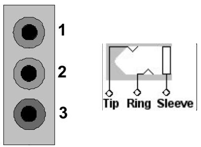
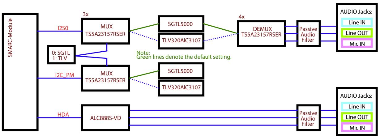
The LEC-BASE 2.0 provides two standard audio jacks for HD (CN153) and I2S (CN155) audio. Two audio codecs support these two interfaces. Figure 2-5 depicts the three lines of the audio jacks: Line In (1 - Blue), Line Out (2 - Green), and MIC In (3 - Pink). Figure 2-6 presents the functional block diagram of I2S and HDA signals connections from the SMARC module to the audio components on the carrier.
![1\n2\n3\nTip Ring Sleeve](.lec-base-2-0-50-1z232-1000-11/f821a1dc6103546c503439a6512c3ae821ff69db5257109295e2d781f787c9f8.jpg)

Figure 2-5: Stereo Jack Configuration
![Based on the provided image, here is the accurate description of the flowchart blocks and connections:\n\n**Blocks:**\n*   **SMARC-Module** (Vertical orientation)\n*   **3x MUX TS5A23157RSER**\n*   **0: SGTL**\n*   **1: TLV**\n*   **SGTL5000** (Two instances)\n*   **TLV320AIC3107** (Two instances)\n*   **Note:** Green lines denote the default setting.\n*   **4x DEMUX TS5A23157RSER**\n*   **Passive Audio Filter** (Two instances)\n*   **AUDIO Jacks:** (Two instances)\n    *   **Line IN**\n    *   **Line OUT**\n    *   **Mic IN**\n*   **I2C_PM**\n*   **HDA**\n*   **ALC888S-VD**\n\n**Connections:**\n*   **SMARC-Module** connects to the **3x MUX TS5A23157RSER** via a line labeled **I250**.\n*   **SMARC-Module** connects to the **0: SGTL / 1: TLV** block, which has blue lines connecting to both the top **MUX TS5A23157RSER** and the middle **MUX TS5A23157RSER**.\n*   **SMARC-Module** connects to the middle **MUX TS5A23157RSER** via a line labeled **I2C_PM**.\n*   **SMARC-Module** connects to the **ALC888S-VD** block via a line labeled **HDA**.\n*   The top **MUX TS5A23157RSER** connects via a green line to the top **SGTL5000** block and via a purple dotted line to the top **TLV320AIC3107** block.\n*   The middle **MUX TS5A23157RSER** connects via a green line to the bottom **SGTL5000** block and via a purple dotted line to the bottom **TLV320AIC3107** block.\n*   Both **SGTL5000** blocks connect via green lines to the **4x DEMUX TS5A23157RSER**.\n*   Both **TLV320AIC3107** blocks connect via purple dotted lines to the **4x DEMUX TS5A23157RSER**.\n*   The **4x DEMUX TS5A23157RSER** connects via blue lines to the top-right **Passive Audio Filter** block.\n*   The top-right **Passive Audio Filter** connects via blue lines to the top-right **AUDIO Jacks:** block (containing **Line IN**, **Line OUT**, **Mic IN**).\n*   The **ALC888S-VD** block connects via three blue lines to the bottom-right **Passive Audio Filter** block.\n*   The bottom-right **Passive Audio Filter** connects via blue lines to the bottom-right **AUDIO Jacks:** block (containing **Line IN**, **Line OUT**, **Mic IN**).](.lec-base-2-0-50-1z232-1000-11/f081b65ce0723a5cc553f5b7e1342c16fc000444dd22cbacaf8a5aca72fcf322.jpg)

Figure 2-6: I2S/HDA Block Diagram

# 2.2.2 PCIe Mini Card Slot

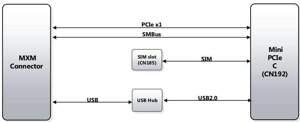
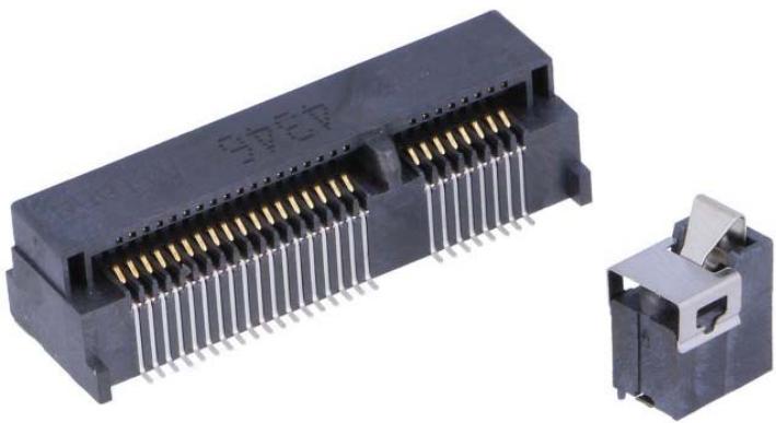
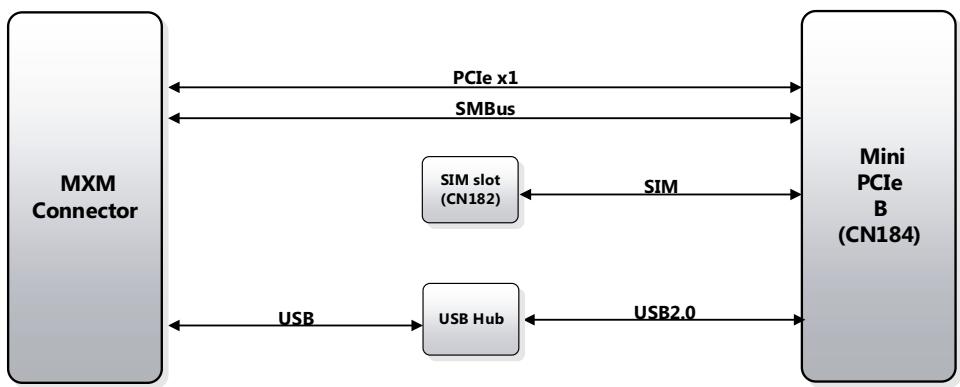
The LEC-BASE 2.0 provides two standard PCI Express Mini Card slots. Figure 2-7 presents one mini card slot with one of the two fastening latches. Figure 2-8 illustrates the functional block diagram of the PCIe Mini Card signals and hardware on the carrier.
![Close-up of a black 375-pin connector with gold pins and terminal slots, shown from two different angles (no text or symbols visible)](.lec-base-2-0-50-1z232-1000-11/d49f015f28c96b0f5cc8e48fa6cbf4e52b6b973f0f83bb74b1aa8da3b30bb49c.jpg)

Figure 2-7: PCIe Mini Card Slot with Latch
![**Blocks:**\n*   **MXM Connector** (Large vertical rectangle on the left)\n*   **Mini PCIe B (CN184)** (Large vertical rectangle on the right)\n*   **SIM slot (CN182)** (Small rectangle in the upper middle)\n*   **USB Hub** (Small rectangle in the lower middle)\n\n**Connections:**\n*   **MXM Connector** connects to **Mini PCIe B (CN184)** via two bidirectional lines labeled **PCIe x1** and **SMBus**.\n*   **SIM slot (CN182)** connects to **Mini PCIe B (CN184)** via a bidirectional line labeled **SIM**.\n*   **USB Hub** connects to **Mini PCIe B (CN184)** via a bidirectional line labeled **USB2.0**.\n*   **MXM Connector** connects to **USB Hub** via a bidirectional line labeled **USB**.](.lec-base-2-0-50-1z232-1000-11/8e92228314059ee4178113374a50e8a703543e50296df786fcefcd7e9a96be08.jpg)

![**Labeled Blocks:**\n*   MXM Connector\n*   SIM slot (CN185)\n*   USB Hub\n*   Mini PCIe C (CN192)\n\n**Connections:**\n*   Between MXM Connector and Mini PCIe C (CN192): PCIe x1\n*   Between MXM Connector and Mini PCIe C (CN192): SMBus\n*   Between SIM slot (CN185) and Mini PCIe C (CN192): SIM\n*   Between MXM Connector and USB Hub: USB\n*   Between USB Hub and Mini PCIe C (CN192): USB2.0](.lec-base-2-0-50-1z232-1000-11/9961b6006a01d2814dd9d4f99d0dca3d9630319cceefee8f52a13ab97ccaadbd.jpg)

Figure 2-8: PCIe Mini Card Slot Block Diagram

# 2.2.3 SD Card Slot

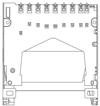
The SD Card slot (CN151) provides the standard 4-bit, push-push interface for SD memory cards. LED5 provides indication of SD power.

![The image features a white document icon with a folded top-right corner. A large red checkmark is centered on the document, which also has faint horizontal lines. Below the graphic, the text 'NOTE:' is displayed in black capital letters.](.lec-base-2-0-50-1z232-1000-11/cb17ee73fe1dd48641edb78d792368304a377ca3fbdeecc472403b3a5ed45ae2.jpg)

UHS cards with 1.8V data signaling are supported. The card supply is always 3.3V regardless if either 1.8V signaling or 3.3V signaling is committed by both card controllers. The SoC and the SD card will agree on which standard they are compatible with and will choose the appropriate standard.
![Top-down schematic of a mechanical or electrical component layout with no visible text, numbers, or symbols.](.lec-base-2-0-50-1z232-1000-11/c9c149765aebe0660ef885d6095b4243c7328acc2f4418ac537254aaac88b769.jpg)

Figure 2-9: SD Card Slot

Table 2-2: SD Card Slot (CN151)

<table><tr><td>Pin #</td><td>Signal</td><td>Description</td><td>Scheme</td></tr><tr><td>1</td><td>SDIO_D3</td><td>SDIO data bit3</td><td rowspan="12">&lt;img src="images/7209b2b282e2707ce14b836d5e582c9b74fc745dceba3a189951f31cb8b3589b.jpg"/&gt;</td></tr><tr><td>2</td><td>SDIO_CMD</td><td>SDIO Command</td></tr><tr><td>3</td><td>GND</td><td>Ground</td></tr><tr><td>4</td><td>+VCC_SDIO</td><td>3.3V power supply</td></tr><tr><td>5</td><td>SDIO_CK</td><td>SDIO clock</td></tr><tr><td>6</td><td>GND</td><td>Ground</td></tr><tr><td>7</td><td>SDIO_D0</td><td>SDIO data bit0</td></tr><tr><td>8</td><td>SDIO_D1</td><td>SDIO data bit1</td></tr><tr><td>9</td><td>SDIO_D2</td><td>SDIO data bit2</td></tr><tr><td>10</td><td>SDIO_CD#</td><td>SDIO card detect</td></tr><tr><td>11</td><td>GND</td><td>Ground</td></tr><tr><td>12</td><td>SDIO_WP</td><td>SDIO write protect</td></tr></table>

Note: Shaded table cells denote power or ground. Use jumper header CN152 to select the SD Card power mode (+V3P3\_SBY or +V3P3S.)

# 2.2.4 SIM Slots

Two SIM slots (CN182 / CN185) provide interface for two Subscriber Identity Modules, supporting both PCIe Mini Card slots: CN182 (SIM1) supports the CN184 Mini Card slot and CN185 (SIM2) supports the CN192 Mini Card slot. Figure 2-10 illustrates the slots' hinge-type connections. Table 2-3 and Table 2-4 provide the signals for both slots.

![Technical line drawing of two mechanical components with mounting holes and internal compartments (no text or symbols)](.lec-base-2-0-50-1z232-1000-11/1b87c54298589a2a48de5638568772a720bfc8a91260484bec0e5b14ab895b8b.jpg)

Figure 2-10: SIM Slots (CN182 / CN185)

Table 2-3: SIM1 Slot (CN182)

<table><tr><td>Pin #</td><td>Signal</td><td>Description</td><td>Scheme</td></tr><tr><td>C1</td><td>UM1_PWR</td><td>+1.8V or +3V VDC power supply input (depending on PCIe Mini Card; +5V is supported if supplied by the Mini Card)</td><td rowspan="8">&lt;img src="images/398ddd9374ab9c976e58b9c0fab4fb9540a7e72cc24b44da49b5402173d0c45d.jpg"/&gt;</td></tr><tr><td>C2</td><td>UM1_RESET</td><td>Resets the card&#x27;s communications</td></tr><tr><td>C3</td><td>UM1_CLK</td><td>Clock signal for data communications timing</td></tr><tr><td>C4</td><td>RES</td><td>Reserved</td></tr><tr><td>C5</td><td>GND</td><td>Ground</td></tr><tr><td>C6</td><td>UM1_VPP</td><td>Programming input voltage</td></tr><tr><td>C7</td><td>UM1_DATA</td><td>I/O for serial data</td></tr><tr><td>C8</td><td>RES</td><td>Reserved</td></tr></table>

NOTE: Shaded table cells denote power or ground.

Table 2-4: SIM2 Slot (CN185)

<table><tr><td>Pin #</td><td>Signal</td><td>Description</td><td>Scheme</td></tr><tr><td>C1</td><td>UM2_PWR</td><td>+1.8V or +3V VDC power supply input (depending on PCIe Mini Card; +5V is supported if supplied by the Mini Card)</td><td rowspan="8">&lt;img src="images/2c87441ef4178dd77d14d57b4f6fb6454d75cbba2a9089c2d700f20a967bac79.jpg"/&gt;</td></tr><tr><td>C2</td><td>UM2_RESET</td><td>Resets the card&#x27;s communications</td></tr><tr><td>C3</td><td>UM2_CLK</td><td>Clock signal for data communications timing</td></tr><tr><td>C4</td><td>RES</td><td>Reserved</td></tr><tr><td>C5</td><td>GND</td><td>Ground</td></tr><tr><td>C6</td><td>UM2_VPP</td><td>Programming input voltage</td></tr><tr><td>C7</td><td>UM2_DATA</td><td>I/O for serial data</td></tr><tr><td>C8</td><td>RES</td><td>Reserved</td></tr></table>

NOTE: Shaded table cells denote power or ground.

# 2.2.5 Battery Socket

One vertical, AAA battery socket provides power for an external RTC coin cell battery. Figure 2-11 illustrates the top and side views of the socket. Table 2-5 provides the signals for the socket.

![This is a black-and-white line drawing of a railway car enclosed within a rectangular border. The car features a flat roof and a long row of windows along the upper section. Below this, on the right side, is a door. Near the bottom of the car body, there is a row of smaller rectangular windows. The undercarriage shows two bogies with wheels and visible suspension springs.](.lec-base-2-0-50-1z232-1000-11/41a6ec423ff7e7a3a312f8945f2a106f736766bac2f6ff516bb651562c1c8ef5.jpg)

![Pure technical diagram of a U-shaped component with three vertical pins at the base (no text or symbols)](.lec-base-2-0-50-1z232-1000-11/2b91f6d696550cb5e77ccaf34acbf953e177573a56842667e39e545861c2c6f9.jpg)

Figure 2-11: Battery Socket

Table 2-5: Battery Socket (BT2)

<table><tr><td>Pin #</td><td>Signal</td><td>Description</td></tr><tr><td>1</td><td>3V_BAT</td><td>+3 volts power for RTC</td></tr><tr><td>2</td><td>GND</td><td>Ground</td></tr><tr><td>3</td><td>3V_BAT</td><td>+3 volts power for RTC</td></tr></table>

Note: Shaded table cells denote power or ground. Jumper required on CN110 to enable the RTC.

![The image displays a warning sign featuring a red triangle with a white exclamation point centered inside it. Below the triangle is a white rectangular background with the black text 'WARNING:' printed in all capital letters.](.lec-base-2-0-50-1z232-1000-11/25f1c90a884a61be9a8739087c3a76fba1db917ed321117973dccc9d8347ae6e.jpg)

A CR2032 battery may explode if incorrectly installed. Replace only with the same or equivalent type recommended by the socket manufacturer.

# 3 Interfaces

This section provides the pin signals for all the non-standard user interfaces on the LEC-BASE 2.0. Unless pinouts for industry standard interfaces have been modified, those pin-out tables will not appear in this manual. Signal definitions for standard interfaces such as RJ45 GbE, SATA, USB, and PCIe can be found in their respective specification datasheets.

![The image features a graphic of a white document with a folded top-right corner and faint horizontal gray lines running through it. A large, red checkmark is superimposed over the center of the document. Below the icon, the text 'NOTE:' appears in black capital letters.](.lec-base-2-0-50-1z232-1000-11/deb8c7fb5cc85085ba9789f3b1178c1a174d6b8beb607383f585b559e987dcde.jpg)

The tables in this section define pin sequence using the method in the following example: A 10-pin header with two rows of pins, using odd/even numbering, where pin 2 is directly across from pin 1, is noted as 10 pins, 2 rows, odd/even pin sequence (1, 2). Consecutive numbering is noted, for example, as 24 pins, 2 rows, consecutive pin sequence (1, 13), where pin 13 is directly across from pin 1. Refer to Figure 2-1 for pin-1 locations.

# 3.1 USB Interfaces

All USB interfaces on the LEC-BASE 2.0 are supported through standard connectors, and their signal definitions can be found in their respective specifications. Sections 3.1.1 through 3.1.11 provide the pinout tables for all the supporting USB jumper headers on the carrier. Refer to the following block diagram for an illustration of the USB interface map on the carrier.

![This block diagram illustrates a connection topology flowing from left to right.\n\n**Leftmost Source Block**\nA tall vertical block contains the following labels:\n*   USB0\n*   USB3\n*   USB2\n*   USB5\n*   USB4\n*   USB1\n\n**Top Connections**\n*   **USB0** connects directly to a block labeled 'USB 2.0 OTG (Micro AB)'.\n*   **USB3** connects to a block labeled 'TUSB501DRFR' (marked '2x'), which connects to a block labeled 'USB 3.0 / 2.0 Type A'.\n*   **USB2** connects to a second block labeled 'TUSB501DRFR' (marked '2x'), which connects to a second block labeled 'USB 3.0 / 2.0 Type A'.\n\n**Middle and Bottom Connections**\n*   **USB5** connects to the top block of a vertical stack.\n*   **USB4** connects to the second block of the same vertical stack.\n*   **USB1** connects to the left side of a block labeled 'USB2514BI'. This block contains internal labels:\n    *   USB11\n    *   USB12\n    *   USB13\n    *   USB14\n*   **USB11** connects to the third block in the vertical stack.\n*   **USB12** connects to the fourth block in the vertical stack.\n*   **USB13** connects to a block labeled 'Mini PCI Express 'B''.\n*   **USB14** connects to a block labeled 'Mini PCI Express 'C''.\n\n**Rightmost Output Blocks**\n*   The four blocks labeled 'USB 2.0' (connected via USB5, USB4, USB11, and USB12) are grouped next to vertical text reading '4x USB 2.0 Type A Stack'.](.lec-base-2-0-50-1z232-1000-11/bed62bfa2345c27c3d45c266f8c8ae55ddaf975e8ddf2f087e41ab60d3d5b621.jpg)

Figure 3-1: USB Mapping Block Diagram

# 3.1.1 USB11 Wake / No Wake Select (CN138)

Table 3-53 lists the pin signals of the USB11 Wake / No Wake select jumper header, which provides 3 pins in a single row with 2.00mm pitch.

Table 3-1: USB11 Wake / No Wake Select (CN138)

<table><tr><td>Pin #</td><td>Signal</td><td>Jumper Positions</td></tr><tr><td>1</td><td>+V5P0_SBY</td><td rowspan="3">• Jumper Installed 1-2 to enable the USB11 Wake from sleep states function [default]• Jumper Installed 2-3 to enable the USB11 No Wake from sleep states function</td></tr><tr><td>2</td><td>+V5P0_USB11</td></tr><tr><td>3</td><td>+V5P0S</td></tr></table>

# 3.1.2 USB12 Wake / No Wake Select (CN139)

Table 3-2 lists the pin signals of the USB12 Wake / No Wake select jumper header, which provides 3 pins in a single row with 2.00mm pitch.

Table 3-2: USB12 Wake / No Wake Select (CN139)

<table><tr><td>Pin #</td><td>Signal</td><td>Jumper Positions</td></tr><tr><td>1</td><td>+V5P0_SBY</td><td rowspan="3">• Jumper Installed 1-2 to enable the USB12 Wake from sleep states function [default]• Jumper Installed 2-3 to enable the USB12 No Wake from sleep states function</td></tr><tr><td>2</td><td>+V5P0_USB12</td></tr><tr><td>3</td><td>+V5P0S</td></tr></table>

# 3.1.3 USB4 Wake / No Wake Select (CN141)

Table 3-3 lists the pin signals of the USB4 Wake / No Wake select jumper header, which provides 3 pins in a single row with 2.00mm pitch.

Table 3-3: USB4 Wake / No Wake Select (CN141)

<table><tr><td>Pin #</td><td>Signal</td><td>Jumper Positions</td></tr><tr><td>1</td><td>+V5P0_SBY</td><td rowspan="3">• Jumper Installed 1-2 to enable the USB4 Wake from sleep states function• Jumper Installed 2-3 to enable the USB4 No Wake from sleep states function [default]</td></tr><tr><td>2</td><td>+V5P0_USB4</td></tr><tr><td>3</td><td>+V5P0S</td></tr></table>

# 3.1.4 USB2 Wake / No Wake Select (CN142)

Table 3-3 lists the pin signals of the USB2 Wake / No Wake select jumper header, which provides 3 pins in a single row with 2.00mm pitch.

Table 3-4: USB2 Wake / No Wake Select (CN142)

<table><tr><td>Pin #</td><td>Signal</td><td>Jumper Positions</td></tr><tr><td>1</td><td>+V5P0_SBY</td><td rowspan="3">• Jumper Installed 1-2 to enable the USB2 Wake from sleep states function• Jumper Installed 2-3 to enable the USB2 No Wake from sleep states function [default]</td></tr><tr><td>2</td><td>+V5P0_USB2</td></tr><tr><td>3</td><td>+V5P0S</td></tr></table>

# 3.1.5 USB5 Wake / No Wake Select (CN143)

Table 3-5 lists the pin signals of the USB5 Wake / No Wake select jumper header, which provides 3 pins in a single row with 2.00mm pitch.

Table 3-5: USB5 Wake / No Wake Select (CN143)

<table><tr><td>Pin #</td><td>Signal</td><td>Jumper Positions</td></tr><tr><td>1</td><td>+V5P0_SBY</td><td rowspan="3">• Jumper Installed 1-2 to enable the USB5 Wake from sleep states function [default]• Jumper Installed 2-3 to enable the USB5 No Wake from sleep states function</td></tr><tr><td>2</td><td>+V5P0_USB5</td></tr><tr><td>3</td><td>+V5P0S</td></tr></table>

# 3.1.6 USB0 Wake / No Wake Select (CN159)

Table 3-6 lists the pin signals of the USB0 Wake / No Wake select jumper header, which provides 3 pins in a single row with 2.00mm pitch.

Table 3-6: USB0 Wake / No Wake Select (CN159)

<table><tr><td>Pin #</td><td>Signal</td><td>Jumper Positions</td></tr><tr><td>1</td><td>+V5P0_SBY</td><td rowspan="3">• Jumper Installed 1-2 to enable the USB0 Wake from sleep states function• Jumper Installed 2-3 to enable the USB0 No Wake from sleep states function [default]</td></tr><tr><td>2</td><td>+V5P0_USB0</td></tr><tr><td>3</td><td>+V5P0S</td></tr></table>

# 3.1.7 USB3 Wake / No Wake Select (CN162)

Table 3-7 lists the pin signals of the USB3 Wake / No Wake select jumper header, which provides 3 pins in a single row with 2.00mm pitch.

Table 3-7: USB3 Wake / No Wake Select (CN162)

<table><tr><td>Pin #</td><td>Signal</td><td>Jumper Positions</td></tr><tr><td>1</td><td>+V5P0_SBY</td><td rowspan="3">• Jumper Installed 1-2 to enable the USB3 Wake from sleep states function• Jumper Installed 2-3 to enable the USB3 No Wake from sleep states function [default]</td></tr><tr><td>2</td><td>+V5P0_USB3</td></tr><tr><td>3</td><td>+V5P0S</td></tr></table>

# 3.1.8 USB4 2.0 Over-Current Detection Source Select (CN211)

Table 3-53 lists the pin signals of the USB4 2.0 Over-Current Detection Source Select jumper header, which provides 3 pins in a single row with 2.00mm pitch.

Table 3-8: USB4 2.0 Over-Current Detection Source Select (CN211)

<table><tr><td>Pin #</td><td>Signal</td><td>Jumper Positions</td></tr><tr><td>1</td><td>USB4_EN_PU</td><td rowspan="3">• Jumper Installed 1-2 to enable the SoC on the Module to detect USB4 over current [default]• Jumper Installed 2-3 to enable the circuits on the carrier to detect USB4 over current</td></tr><tr><td>2</td><td>USB4_EN</td></tr><tr><td>3</td><td>USB4_EN_OC#</td></tr></table>

NOTE: The # symbol indicates the signal is Active Low.

# 3.1.9 USB5 2.0 Over-Current Detection Source Select (CN212)

Table 3-53 lists the pin signals of the USB5 2.0 Over-Current Detection Source Select jumper header, which provides 3 pins in a single row with 2.00mm pitch.

Table 3-9: USB5 2.0 Over-Current Detection Source Select (CN212)

<table><tr><td>Pin #</td><td>Signal</td><td>Jumper Positions</td></tr><tr><td>1</td><td>USB5_EN_PU</td><td rowspan="3">• Jumper Installed 1-2 to enable the SoC on the Module to detect USB5 over current [default]• Jumper Installed 2-3 to enable the circuits on the carrier to detect USB5 over current</td></tr><tr><td>2</td><td>USB5_EN</td></tr><tr><td>3</td><td>USB5_EN_OC#</td></tr></table>

NOTE: The # symbol indicates the signal is Active Low.

# 3.1.10 USB3 3.0 Over-Current Detection Source Select (CN213)

Table 3-53 lists the pin signals of the USB3 3.0 Over-Current Detection Source Select jumper header, which provides 3 pins in a single row with 2.00mm pitch.

Table 3-10: USB3 3.0 Over-Current Detection Source Select (CN213)

<table><tr><td>Pin #</td><td>Signal</td><td>Jumper Positions</td></tr><tr><td>1</td><td>USB3_EN_PU</td><td rowspan="3">• Jumper Installed 1-2 to enable the SoC on the Module to detect USB3 over current [default]• Jumper Installed 2-3 to enable the circuits on the carrier to detect USB3 over current</td></tr><tr><td>2</td><td>USB3_EN</td></tr><tr><td>3</td><td>USB3_EN_OC#</td></tr></table>

NOTE: The # symbol indicates the signal is Active Low.

# 3.1.11 USB2 3.0 Over-Current Detection Source Select (CN214)

Table 3-53 lists the pin signals of the USB2 3.0 Over-Current Detection Source Select jumper header, which provides 3 pins in a single row with 2.00mm pitch.

Table 3-11: USB2 3.0 Over-Current Detection Source Select (CN214)

<table><tr><td>Pin #</td><td>Signal</td><td>Jumper Positions</td></tr><tr><td>1</td><td>USB2_EN_PU</td><td rowspan="3">• Jumper Installed 1-2 to enable the SoC on the Module to detect USB2 over current [default]• Jumper Installed 2-3 to enable the circuits on the carrier to detect USB2 over current</td></tr><tr><td>2</td><td>USB2_EN</td></tr><tr><td>3</td><td>USB2_EN_OC#</td></tr></table>

NOTE: The # symbol indicates the signal is Active Low.

# 3.2 Power Interfaces

This section describes the signals for all power interfaces on the carrier, including ATX, RTC battery, and Smart Battery (BattMan) input interfaces.

# 3.2.1 ATX Power (CN2)

Table 3-12 lists the signals of the standard ATX Power connector, which provides 24 pins, 2 rows consecutive pin sequence (1, 13) with 4.20mm pitch. Use the SW34 button switch on the carrier to apply power to the module\*.

Table 3-12: ATX Power Signals (CN2)

<table><tr><td>Pin#</td><td>Signal</td><td>Description</td><td>Pin#</td><td>Signal</td><td>Description</td></tr><tr><td>1</td><td>+V3P3_ATX</td><td>Power Supply DC voltage</td><td>13</td><td>+V3P3_ATX</td><td>Power Supply DC voltage</td></tr><tr><td>2</td><td>+V3P3_ATX</td><td>Power Supply DC voltage</td><td>14</td><td>NC</td><td>Not Connected</td></tr><tr><td>3</td><td>GND</td><td>Ground</td><td>15</td><td>GND</td><td>Ground</td></tr><tr><td>4</td><td>+V5P0_ATX</td><td>Power Supply DC voltage</td><td>16</td><td>ATX_PS_ON#</td><td>Switch to turn on power supply, shorted to Ground</td></tr><tr><td>5</td><td>GND</td><td>Ground</td><td>17</td><td>GND</td><td>Ground</td></tr><tr><td>6</td><td>+V5P0_ATX</td><td>Power Supply DC voltage</td><td>18</td><td>GND</td><td>Ground</td></tr><tr><td>7</td><td>GND</td><td>Ground</td><td>19</td><td>GND</td><td>Ground</td></tr><tr><td>8</td><td>ATX_PWRGD</td><td>Status from the power supply, notifying the computer that the DC operating voltages are within the required ranges</td><td>20</td><td>NC</td><td>Not Connected</td></tr><tr><td>9</td><td>+V5P0_SBY</td><td>Power Supply Standby DC voltage</td><td>21</td><td>+V5P0_ATX</td><td>Power Supply DC voltage</td></tr><tr><td>10</td><td>+V12P0_ATX</td><td>Power Supply DC voltage</td><td>22</td><td>+V5P0_ATX</td><td>Power Supply DC voltage</td></tr><tr><td>11</td><td>+V12P0_ATX</td><td>Power Supply DC voltage</td><td>23</td><td>+V5P0_ATX</td><td>Power Supply DC voltage</td></tr><tr><td>12</td><td>+V3P3_ATX</td><td>Power Supply DC voltage</td><td>24</td><td>GND</td><td>Ground</td></tr></table>

NOTE: Shaded table cells denote power or ground. The # symbol indicates the signal is Active Low.
\*As soon as an active ATX power supply is connected to the carrier, the module will be receiving power. The power button is used for starting the system power-up sequence. The module controls power up and power down of the carrier.

# 3.2.2 Battery Interface (CN111)

Table 3-13 lists the pin signals of the battery interface header, which provides 2 pins in a single row with 1.25mm pitch.

Table 3-13: Battery Interface (CN111)

<table><tr><td>Pin #</td><td>Signal</td></tr><tr><td>1</td><td>+VDD_RTC_IN</td></tr><tr><td>2</td><td>GND</td></tr></table>

NOTE: Shaded table cells denote power or ground.

# 3.2.3 Battery Enable (CN110)

Table 3-14 lists the pin signals of the RTC battery enable jumper header, which provides 2 pins in a single row with 2mm pitch.

Table 3-14: Battery Enable (CN110)

<table><tr><td>Pin #</td><td>Signal</td><td>Jumper Positions</td></tr><tr><td>1</td><td>+VDD_RTC_IN</td><td rowspan="2">• Jumper installed to connect RTC battery [default]• Jumper removed to disconnect RTC battery</td></tr><tr><td>2</td><td>+VDD_RTC_CON</td></tr></table>

# 3.2.4 Smart Battery (BattMan) Interface (CN128)

Table 3-15 lists the pin signals of the Smart Battery header, which provides 10 pins in 2 rows, odd/even pin sequence (1, 2), and 2.54mm pitch.

![The image displays a yellow triangular warning sign with a black border. Inside the triangle is a black exclamation point. Below the triangle, the word 'CAUTION:' appears in black, uppercase letters.](.lec-base-2-0-50-1z232-1000-11/4e7cf5c633855249c82682f1700bc3a847f9bd3a53ab1f3ea512d60287b8f322.jpg)

You must configure the jumper settings as described in Table 3-15, or system damage could occur when using a BattMan power supply to Power On the carrier.

Table 3-15: Smart Battery (BattMan) Interface (CN128)

<table><tr><td>Pin #</td><td>Signal</td><td>Jumper Configurations</td></tr><tr><td>1</td><td>SMB_BATT_SCL (serial clock)</td><td rowspan="10">Make sure to set following jumper configurations before implementing a BattMan power supply to Power On the carrier:• Pins 1-2 on CN129, BattMan voltage select for battery-side SMBUS• Pins 2-3 on CN206, BattMan enable</td></tr><tr><td>2</td><td>SMB_BATT_SDA (serial data)</td></tr><tr><td>3</td><td>BATT_PWR_BTN#</td></tr><tr><td>4</td><td>BATTLOWJ</td></tr><tr><td>5</td><td>BATT_PS_ON (ATX power supply)</td></tr><tr><td>6</td><td>Not Connected</td></tr><tr><td>7</td><td>+V12P0_ATX (12-volt power)</td></tr><tr><td>8</td><td>+V5P0_SBY (5-volt standby power)</td></tr><tr><td>9</td><td>SMB_ALERT# (SMBus alert)</td></tr><tr><td>10</td><td>GND</td></tr></table>

NOTE: The voltage level of this interface is determined by the CN129 jumper header (default 5V for BattMan supply.) Shaded table cells denote power or ground.

# 3.2.5 BattMan SMBus Voltage Select (CN129)

Table 3-16 lists the pin signals of the BattMan SMBus voltage select jumper header, which provides 3 pins in a single row with 2.00mm pitch.

Table 3-16: BattMan SMBus Voltage Select (CN129)

<table><tr><td>Pin #</td><td>Signal</td><td>Jumper Positions</td></tr><tr><td>1</td><td>+V5P0_SBY</td><td rowspan="3">Jumper Installed 1-2 - 5-volt +VCC_SMB_BATT [default]Jumper Installed 2-3 - 3.3-volt +VCC_SMB_BATT</td></tr><tr><td>2</td><td>+VCC_SMB_BATT</td></tr><tr><td>3</td><td>+V3PS_SBY</td></tr></table>

# 3.2.6 BattMan Charger Interface (CN202)

Table 3-17 lists the pin signals of the BattMan Charger interface, which provides 6 pins in two rows with odd/even pin sequence (1,2) and 2.00mm pitch.

Table 3-17: BattMan Charger Interface (CN202)

<table><tr><td>Pin #</td><td>Signal</td><td>Pin #</td><td>Signal</td></tr><tr><td>1</td><td>BATMAN.BATLOW# (1.8V logic)</td><td>2</td><td>BATMAN.CHARGER_PRSNT# (1.8V logic)</td></tr><tr><td>3</td><td>GND</td><td>4</td><td>GND</td></tr><tr><td>5</td><td>BATMAN.CHARGING# (1.8V logic)</td><td>6</td><td>GND</td></tr></table>

NOTE: Shaded table cells denote ground. The # symbol indicates the signal is Active Low.

# 3.2.7 BattMan Enable (CN206)

Table 3-18 lists the pin signals of the BattMan enable jumper header, which provides 3 pins in a single row with 2.00mm pitch.

Table 3-18: BattMan Enable (CN206)

<table><tr><td>Pin #</td><td>Signal</td><td>Jumper Positions</td></tr><tr><td>1</td><td>GND</td><td rowspan="3">Jumper on 1-2 disables BattMan support [default]Jumper on 2-3 enables BattMan support</td></tr><tr><td>2</td><td>EN_VR50_BATT</td></tr><tr><td>3</td><td>+V5P0_SBY</td></tr></table>

# 3.3 Display Interfaces

The LEC-BASE 2.0 supports four display interfaces, with the capacity to use three of them, simultaneously. This section provides the pinout tables for all four interfaces including the pinout tables for all support interfaces and jumper headers. The following list presents the four display interfaces.

▶ LVDS
▶ eDP (embedded DisplayPort)
▶ HDMI
▶ DP++ (Dual-Mode DisplayPort)

# 3.3.1 LVDS (CN25)

Table 3-19 lists the pin signals of the LVDS header which provides 34-pins, 2 rows, odd/even pin sequence (1, 2) with 2.00mm pitch. Channel A pins are connected directly to the LVDS interface at the SMARC connector. Channel B pins are connected to selected LCD pins on the SMARC connector.

NOTE: The shaded table cells denote power or ground.
\* If using an LVDS panel without EDID-ROM, disconnect pin 4 by removing the R551 solder jumper.
Table 3-19: LVDS Interface Pin Signals (CN25)

<table><tr><td>Pin #</td><td>Signal</td><td>Description</td><td>SMARC Signal</td></tr><tr><td>1</td><td>LVDS_DDC_DAT</td><td>System Management Data</td><td>I2C_LCD_DAT</td></tr><tr><td>2</td><td>LVDS_DDC_CLK</td><td>System Management Clock</td><td>I2C_LCD_DAT</td></tr><tr><td>3</td><td>+VDD_LVDS</td><td>Panel Power [use CN114 and CN117 jumper headers to select voltages and +VCC display modes]</td><td>N/A</td></tr><tr><td>4</td><td>+VDD_LVDS_EDID*</td><td>Panel EDID Power [use R551 and R1391 solder jumpers to select voltages +V3P3_SBY (R551 [default]) or +VDD_PANEL (R1391)] *</td><td>N/A</td></tr><tr><td>5</td><td>GND</td><td>Ground</td><td>GND</td></tr><tr><td>6</td><td>LVDS_A0_N</td><td>Data Negative Output - Channel A</td><td>LVDS0_0-</td></tr><tr><td>7</td><td>LVDS_A0_P</td><td>Data Positive Output - Channel A</td><td>LVDS0_0+</td></tr><tr><td>8</td><td>LVDS_VDDEN</td><td>Panel Power Enable</td><td>LCD_VDD_EN</td></tr><tr><td>9</td><td>LVDS_A1_N</td><td>Data Negative Output - Channel A</td><td>LVDS0_1-</td></tr><tr><td>10</td><td>LVDS_A1_P</td><td>Data Positive Output - Channel A</td><td>LVDS0_1+</td></tr><tr><td>11</td><td>LVDS_BKLT_EN</td><td>Panel Backlight Enable</td><td>LCD_BKLT_EN</td></tr><tr><td>12</td><td>LVDS_A2_P</td><td>Data Positive Output - Channel A</td><td>LVDS0_2+</td></tr><tr><td>13</td><td>LVDS_A2_N</td><td>Data Negative Output - Channel A</td><td>LVDS0_2-</td></tr><tr><td>14</td><td>NC</td><td>Not Connected</td><td></td></tr><tr><td>15</td><td>LVDS_A_CK_N</td><td>Clock Negative - Channel A</td><td>LVDS0_CK-</td></tr><tr><td>16</td><td>LVDS_A_CK_P</td><td>Clock Positive - Channel A</td><td>LVDS0_CK+</td></tr><tr><td>17</td><td>+VDD_LVDS</td><td>Panel Power [use CN114 and CN117 jumper headers to select voltages and +VCC display modes]</td><td>N/A</td></tr><tr><td>18</td><td>LVDS_A3_P</td><td>Data Positive Output - Channel A</td><td>LVDS0_3+</td></tr><tr><td>19</td><td>LVDS_A3_N</td><td>Data Negative Output - Channel A</td><td>LVDS0_3-</td></tr><tr><td>20</td><td>GND</td><td>Ground</td><td></td></tr><tr><td>21</td><td>LVDS_B0_N</td><td>Data Negative Output - Channel B</td><td>LVDS1_0-</td></tr><tr><td>22</td><td>LVDS_B0_P</td><td>Data Positive Output - Channel B</td><td>LVDS1_0+</td></tr><tr><td>23</td><td>GND</td><td>Ground</td><td></td></tr><tr><td>24</td><td>LVDS_B1_N</td><td>Data Negative Output - Channel B</td><td>LVDS1_1-</td></tr><tr><td>25</td><td>LVDS_B1_P</td><td>Data Positive Output - Channel B</td><td>LVDS1_1+</td></tr><tr><td>26</td><td>GND</td><td>Ground</td><td></td></tr><tr><td>27</td><td>LVDS_B2_N</td><td>Data Negative Output - Channel B</td><td>LVDS1_2-</td></tr><tr><td>28</td><td>LVDS_B2_P</td><td>Data Positive Output - Channel B</td><td>LVDS1_2+</td></tr><tr><td>29</td><td>GND</td><td>Ground</td><td></td></tr><tr><td>30</td><td>LVDS_B_CK_P</td><td>Clock Positive - Channel B</td><td>LVDS1_CK+</td></tr><tr><td>31</td><td>LVDS_B_CK_N</td><td>Clock Negative - Channel B</td><td>LVDS1_CK-</td></tr><tr><td>32</td><td>NC</td><td>Not Connected</td><td></td></tr><tr><td>33</td><td>LVDS_B3_P</td><td>Data Positive - Channel B</td><td>LVDS1_3+</td></tr><tr><td>34</td><td>LVDS_B3_N</td><td>Data Negative - Channel B</td><td>LVDS1_3-</td></tr></table>

# 3.3.2 LVDS Backlight 0 (CN116)

Table 3-20 lists the pin signals of the LVDS Backlight 0 interface, which provides 8 pins, 2 rows, with odd/even pin sequence (1, 2) and 2.54mm pitch.

Table 3-20: LVDS Backlight 0 (CN116)

<table><tr><td>Pin #</td><td>Signal</td></tr><tr><td>1</td><td>GND</td></tr><tr><td>2</td><td>+VDD_PANEL(VDD fixed voltages 3.3V or 5V selected at CN117; or switch to +VCC_PANEL mode at CN117 (3-4) and select VCC voltages at CN114).</td></tr><tr><td>3</td><td>LVDS_BKLT0_CTRL</td></tr><tr><td>4</td><td>GND</td></tr><tr><td>5</td><td>LVDS_BKLT0_EN</td></tr><tr><td>6</td><td>GND</td></tr><tr><td>7</td><td>Not Connected</td></tr><tr><td>8</td><td>+VCC_BKLT (backlight voltage, controlled by chipset and selected at CN207)</td></tr></table>

NOTE: The shaded table cells denote Ground or Power.

![The image depicts a yellow triangular warning sign with a black border and a black exclamation point in the center. Below the triangle, the text 'CAUTION:' appears in bold black capital letters.](.lec-base-2-0-50-1z232-1000-11/154293a695d2f3de04cf0b71eb9b835c193171fe3ae79174716df7017c652a9d.jpg)

Never select +12V for +VCC\_Panel (jumper on pins 3-4) at CN114 while in +VDD\_Panel mode (jumper on 1-2 or 5-6 at CN117.) Doing so will destroy the LVDS control circuitry

# 3.3.3 LVDS Backlight 1 (CN113)

Table 3-21 lists the pin signals of the LVDS Backlight 1 interface, which provides 8 pins, 2 rows, with odd/even pin sequence (1, 2) and 2.54mm pitch.

Table 3-21: LVDS Backlight 1 (CN113)

<table><tr><td>Pin #</td><td>Signal</td></tr><tr><td>1</td><td>GND</td></tr><tr><td>2</td><td>+VDD_PANEL(VDD fixed voltages 3.3V or 5V selected at CN117; or switch to +VCC_PANEL mode at CN117 (3-4) and select VCC voltages at CN114)</td></tr><tr><td>3</td><td>LVDS_BKLT1_CTRL</td></tr><tr><td>4</td><td>GND</td></tr><tr><td>5</td><td>LVDS_BKLT1_EN</td></tr><tr><td>6</td><td>GND</td></tr><tr><td>7</td><td>Not Connected</td></tr><tr><td>8</td><td>+VCC_BKLT (backlight voltage, controlled by chipset and selected at CN207)</td></tr></table>

NOTE: The shaded table cells denote Ground or Power.

![The image displays a standard safety warning sign. It features a yellow equilateral triangle with a black border containing a black exclamation point in the center. Below the triangle is a white rectangular bar with the word 'CAUTION:' printed in bold, black, capital letters.](.lec-base-2-0-50-1z232-1000-11/96bd52448b2a2e4f255e2d7af9c52f9245b6e9bf192d4c6495e74172c427f155.jpg)

Never select +12V for +VCC\_Panel (jumper on pins 3-4) at CN114 while in +VDD\_Panel mode (jumper on 1-2 or 5-6 at CN117.) Doing so will destroy the LVDS control circuitry.

# 3.3.4 LVDS VCC Voltage Select (CN114)

Table 3-22 lists the pin signals of the LVDS VCC Voltage Select jumper header, which provides 6 pins in two rows with odd/even pin sequence (1,2) and 2mm pitch.

Table 3-22: LVDS VCC Voltage Select Signals (CN114)

<table><tr><td>Pin #</td><td>Signal</td><td>Pin #</td><td>Signal</td><td>Jumper Positions</td></tr><tr><td>1</td><td>+VLCD_3P3</td><td>2</td><td>+VCC_PANEL_IN</td><td rowspan="3">• Pins 1-2 for selecting +3.3V LVDS VCC panel voltage [default]• Pins 3-4 for selecting +12V LVDS VCC panel voltage• Pins 5-6 for selecting +5V LVDS VCC panel voltage</td></tr><tr><td>3</td><td>+VLCD_12P0</td><td>4</td><td>+VCC_PANEL_IN</td></tr><tr><td>5</td><td>+VLCD_5P0</td><td>6</td><td>+VCC_PANEL_IN</td></tr></table>

NOTE: A jumper must be placed on pins 3-4 of header CN117 to enable VCC mode.

# 3.3.5 LVDS VDD Voltage Select (CN117)

Table 3-22 lists the pin signals of the LVDS VDD Voltage Select jumper header, which provides 6 pins in two rows with odd/even pin sequence (1,2) and 2mm pitch.

Table 3-23: LVDS Voltage Select Signals (CN117)

<table><tr><td>Pin #</td><td>Signal</td><td>Pin #</td><td>Signal</td><td>Jumper Positions</td></tr><tr><td>1</td><td>+VLCD_3P3</td><td>2</td><td>+VDD_PANEL_IN</td><td rowspan="3">• Pins 1-2 for selecting +3.3V LVDS VDD panel voltage• Pins 3-4 for enabling LVDS VCC mode [default]• Pins 5-6 for selecting +5V LVDS VDD panel voltage</td></tr><tr><td>3</td><td>+VCC_PANEL</td><td>4</td><td>+VDD_PANEL_IN</td></tr><tr><td>5</td><td>+VLCD_5P0</td><td>6</td><td>+VDD_PANEL_IN</td></tr></table>

NOTE: Move jumper to 1-2 or 5-6 to enable VDD mode.

# 3.3.6 LVDS / eDP Mode Select (CN120)

Table 3-22 lists the pin signals of the LVDS / EDP Mode Select jumper header, which provides 6 pins in two rows with odd/even pin sequence (1,2) and 2mm pitch.

Table 3-24: LVDS / eDP mode Select (CN120)

<table><tr><td>Pin #</td><td>Signal</td><td>Pin #</td><td>Signal</td><td>Jumper Positions</td></tr><tr><td>1</td><td>LVDS_eDP_SEL_R*</td><td>2</td><td>Not Connected</td><td rowspan="3">• Pins 1-3 for selecting eDP mode• Pins 4-6 for selecting LVDS mode [default]</td></tr><tr><td>3</td><td>LVDS_eDP_SEL</td><td>4</td><td>LVDS_eDP_SEL</td></tr><tr><td>5</td><td>Not Connected</td><td>6</td><td>GND</td></tr></table>

\* Pin-1 signal = +V3P3S with 4.7K PU

# 3.3.7 Backlight Voltage Select (CN207)

Table 3-25 lists the pin signals of the Backlight Voltage select jumper header, which provides 6 pins in two rows with odd/even pin sequence (1,2) and 2.54mm pitch.

Table 3-25: Backlight Voltage Select (CN207)

<table><tr><td>Pin #</td><td>Signal</td><td>Pin #</td><td>Signal</td><td>Jumper Positions</td></tr><tr><td>1</td><td>+VLCD_12P0</td><td>2</td><td>+VCC_BKL_IN</td><td rowspan="4">• Jumpers on 1-2 and 3-4 selects 12V supply to backlight (both jumpers needed in case of high-powered backlights) [default]• Jumper on 7-8 selects 5V supply to backlight</td></tr><tr><td>3</td><td>+VLCD_12P0</td><td>4</td><td>+VCC_BKL_IN</td></tr><tr><td>5</td><td>Not Connected</td><td>6</td><td>Not Connected</td></tr><tr><td>7</td><td>+VLCD_5P0</td><td>8</td><td>+VCC_BKL_IN</td></tr></table>

# 3.3.8 eDP0 (CN121)

Table 3-26 lists the pin signals of the embedded DisplayPort 0 connector, which provides 40-pins, single row with 0.5mm pitch.

NOTE: The shaded table cells denote power or ground.
Table 3-26: eDP0 Video Signals (CN121)

<table><tr><td>Pin #</td><td>Signal</td><td>Description</td></tr><tr><td>1</td><td>NC</td><td>Not Connected</td></tr><tr><td>2</td><td>eDP0_BKLT_PWR</td><td>Backlight power (5V / 12V [selected at CN59])</td></tr><tr><td>3</td><td>eDP0_BKLT_PWR</td><td>Backlight power (5V / 12V [selected at CN59])</td></tr><tr><td>4</td><td>eDP0_BKLT_PWR</td><td>Backlight power (5V / 12V [selected at CN59])</td></tr><tr><td>5</td><td>eDP0_BKLT_PWR</td><td>Backlight power (5V / 12V [selected at CN59])</td></tr><tr><td>6</td><td>NC</td><td>Not Connected</td></tr><tr><td>7</td><td>NC</td><td>Not Connected</td></tr><tr><td>8</td><td>eDP0_BKLT_PWM</td><td>Backlight brightness via pulse width modulation (PWM)</td></tr><tr><td>9</td><td>eDP0_BKLT_ENABLE</td><td>Backlight power enable</td></tr><tr><td>10</td><td>eDP0_BKLT_GND</td><td>Backlight ground</td></tr><tr><td>11</td><td>eDP0_BKLT_GND</td><td>Backlight ground</td></tr><tr><td>12</td><td>eDP0_BKLT_GND</td><td>Backlight ground</td></tr><tr><td>13</td><td>eDP0_BKLT_GND</td><td>Backlight ground</td></tr><tr><td>14</td><td>eDP0_HPD</td><td>Hot Plug Detect</td></tr><tr><td>15</td><td>eDP0_LCD_GND</td><td>LCD ground</td></tr><tr><td>16</td><td>eDP0_LCD_GND</td><td>LCD ground</td></tr><tr><td>17</td><td>eDP0_LCD_GND</td><td>LCD ground</td></tr><tr><td>18</td><td>eDP0_LCD_GND</td><td>LCD ground</td></tr><tr><td>19</td><td>NC</td><td>Not Connected</td></tr><tr><td>20</td><td>eDP0_LCD_VCC</td><td>LCD power (3.3V / 5V / 12V)</td></tr><tr><td>21</td><td>eDP0_LCD_VCC</td><td>LCD power (3.3V / 5V / 12V)</td></tr><tr><td>22</td><td>eDP0_LCD_VCC</td><td>LCD power (3.3V / 5V / 12V)</td></tr><tr><td>23</td><td>eDP0_LCD_VCC</td><td>LCD power (3.3V / 5V / 12V)</td></tr><tr><td>24</td><td>eDP0_HS_GND</td><td>High-Speed Ground</td></tr><tr><td>25</td><td>eDP0_AUX_n</td><td>Auxiliary differential pair - negative</td></tr><tr><td>26</td><td>eDP0_AUX_p</td><td>Auxiliary differential pair - positive</td></tr><tr><td>27</td><td>eDP0_HS_GND</td><td>High-Speed Ground</td></tr><tr><td>28</td><td>eDP0_TX0_p</td><td>Lane 0 Display Port primary channel differential pair 0 - positive</td></tr><tr><td>29</td><td>eDP0_TX0_n</td><td>Lane 0 Display Port primary channel differential pair 0 - negative</td></tr><tr><td>30</td><td>eDP0_HS_GND</td><td>High-Speed Ground</td></tr><tr><td>31</td><td>eDP0_TX1_p</td><td>Lane 1 Display Port primary channel differential pair 1 - positive</td></tr><tr><td>32</td><td>eDP0_TX1_n</td><td>Lane 1 Display Port primary channel differential pair 1 - negative</td></tr><tr><td>33</td><td>eDP0_HS_GND</td><td>High-Speed Ground</td></tr><tr><td>34</td><td>eDP0_TX2_p</td><td>Lane 2 Display Port primary channel differential pair 2 - positive</td></tr><tr><td>35</td><td>eDP0_TX2_n</td><td>Lane 2 Display Port primary channel differential pair 2 - negative</td></tr><tr><td>36</td><td>eDP0_HS_GND</td><td>High-Speed Ground</td></tr><tr><td>37</td><td>eDP0_TX3_p</td><td>Lane 3 Display Port primary channel differential pair 3 - positive</td></tr><tr><td>38</td><td>eDP0_TX3_n</td><td>Lane 3 Display Port primary channel differential pair 3 - negative</td></tr><tr><td>39</td><td>eDP0_HS_GND</td><td>High-Speed Ground</td></tr><tr><td>40</td><td>NC</td><td>Not Connected</td></tr></table>

# 3.3.9 eDP1 (CN118)

Table 3-27 lists the pin signals of the embedded DisplayPort 1 connector, which provides 40-pins, single row with 0.5mm pitch.

Table 3-27: eDP1 Video Signals (CN118)

<table><tr><td>Pin #</td><td>Signal</td><td>Description</td></tr><tr><td>1</td><td>NC</td><td>Not Connected</td></tr><tr><td>2</td><td>eDP1_BKLT_PWR</td><td>Backlight power (5V / 12V [selected at CN207])</td></tr><tr><td>3</td><td>eDP1_BKLT_PWR</td><td>Backlight power (5V / 12V [selected at CN207])</td></tr><tr><td>4</td><td>eDP1_BKLT_PWR</td><td>Backlight power (5V / 12V [selected at CN207])</td></tr><tr><td>5</td><td>eDP1_BKLT_PWR</td><td>Backlight power (5V / 12V [selected at CN207])</td></tr><tr><td>6</td><td>NC</td><td>Not Connected</td></tr><tr><td>7</td><td>NC</td><td>Not Connected</td></tr><tr><td>8</td><td>eDP1_BKLT_PWM</td><td>Backlight brightness via pulse width modulation (PWM)</td></tr><tr><td>9</td><td>eDP1_BKLT_ENABLE</td><td>Backlight power enable</td></tr><tr><td>10</td><td>eDP1_BKLT_GND</td><td>Backlight ground</td></tr><tr><td>11</td><td>eDP1_BKLT_GND</td><td>Backlight ground</td></tr><tr><td>12</td><td>eDP1_BKLT_GND</td><td>Backlight ground</td></tr><tr><td>13</td><td>eDP1_BKLT_GND</td><td>Backlight ground</td></tr><tr><td>14</td><td>eDP1_HPD</td><td>Hot Plug Detect</td></tr><tr><td>15</td><td>eDP1_LCD_GND</td><td>LCD ground</td></tr><tr><td>16</td><td>eDP1_LCD_GND</td><td>LCD ground</td></tr><tr><td>17</td><td>eDP1_LCD_GND</td><td>LCD ground</td></tr><tr><td>18</td><td>eDP1_LCD_GND</td><td>LCD ground</td></tr><tr><td>19</td><td>NC</td><td>Not Connected</td></tr><tr><td>20</td><td>eDP1_LCD_VCC</td><td>LCD power (3.3V / 5V / 12V)</td></tr><tr><td>21</td><td>eDP1_LCD_VCC</td><td>LCD power (3.3V / 5V / 12V)</td></tr><tr><td>22</td><td>eDP1_LCD_VCC</td><td>LCD power (3.3V / 5V / 12V)</td></tr><tr><td>23</td><td>eDP1_LCD_VCC</td><td>LCD power (3.3V / 5V / 12V)</td></tr><tr><td>24</td><td>eDP1_HS_GND</td><td>High-Speed Ground</td></tr><tr><td>25</td><td>eDP1_AUX_n</td><td>Auxiliary differential signal - negative</td></tr><tr><td>26</td><td>eDP1_AUX_p</td><td>Auxiliary differential signal - positive</td></tr><tr><td>27</td><td>eDP1_HS_GND</td><td>High-Speed Ground</td></tr><tr><td>28</td><td>eDP1_TX0_p</td><td>Lane 0 Display Port primary channel differential signal 0 - positive</td></tr><tr><td>29</td><td>eDP1_TX0_n</td><td>Lane 0 Display Port primary channel differential signal 0 - negative</td></tr><tr><td>30</td><td>eDP1_HS_GND</td><td>High-Speed Ground</td></tr><tr><td>31</td><td>eDP1_TX1_p</td><td>Lane 1 Display Port primary channel differential signal 1 - positive</td></tr><tr><td>32</td><td>eDP1_TX1_n</td><td>Lane 1 Display Port primary channel differential signal 1 - negative</td></tr><tr><td>33</td><td>eDP1_HS_GND</td><td>High-Speed Ground</td></tr><tr><td>34</td><td>eDP1_TX2_p</td><td>Lane 2 Display Port primary channel differential signal 2 - positive</td></tr><tr><td>35</td><td>eDP1_TX2_n</td><td>Lane 2 Display Port primary channel differential signal 2 - negative</td></tr><tr><td>36</td><td>eDP1_HS_GND</td><td>High-Speed Ground</td></tr><tr><td>37</td><td>eDP1_TX3_p</td><td>Lane 3 Display Port primary channel differential signal 3 - positive</td></tr><tr><td>38</td><td>eDP1_TX3_n</td><td>Lane 3 Display Port primary channel differential signal 3 - negative</td></tr><tr><td>39</td><td>eDP1_HS_GND</td><td>High-Speed Ground</td></tr><tr><td>40</td><td>NC</td><td>Not Connected</td></tr></table>

NOTE: The shaded table cells denote power or ground.

# 3.3.10 HDMI (CN123)

Table 3-31 lists the pin signals of the HDMI interface, which provides a 19-pin, standard two-row connector with 0.5mm pitch.

Table 3-28: HDMI Signals (CN123)

<table><tr><td>Pin #</td><td>Signal</td><td>Description</td><td>Pin Sequence</td></tr><tr><td>1</td><td>HDMI_D2_P</td><td>Data2 differential signal - Positive</td><td rowspan="19">&lt;img src="images/9724b1a08bed7c19d78f95959375b8b7080a4aec7e17f9006e7e85b9af47a184.jpg"/&gt;HDMI Type APlug Connector</td></tr><tr><td>2</td><td>GND</td><td>Data2 Ground</td></tr><tr><td>3</td><td>HDMI_D2_N</td><td>Data2 differential signal - Negative</td></tr><tr><td>4</td><td>HDMI_D1_P</td><td>Data1 differential signal - Positive</td></tr><tr><td>5</td><td>GND</td><td>Data1 Ground</td></tr><tr><td>6</td><td>HDMI_D1_N</td><td>Data1 differential signal - Negative</td></tr><tr><td>7</td><td>HDMI_D0_P</td><td>Data0 differential signal - Positive</td></tr><tr><td>8</td><td>GND</td><td>Data0 Ground</td></tr><tr><td>9</td><td>HDMI_D0_N</td><td>Data0 differential signal - Negative</td></tr><tr><td>10</td><td>HDMI_CK_P</td><td>Clock - Positive</td></tr><tr><td>11</td><td>GND</td><td>Clock Ground</td></tr><tr><td>12</td><td>HDMI_CK_N</td><td>Clock - Negative</td></tr><tr><td>13</td><td>HDMI_CEC</td><td>Consumer Electronics Control bus</td></tr><tr><td>14</td><td>NC</td><td>Not Connected</td></tr><tr><td>15</td><td>HDMI_SCL</td><td>I2C Serial Clock for DDC</td></tr><tr><td>16</td><td>HDMI_SDA</td><td>I2C Serial Data for DDC</td></tr><tr><td>17</td><td>GND</td><td>DDC / CEC Ground</td></tr><tr><td>18</td><td>HDMI_+5V</td><td>5 Volts Power</td></tr><tr><td>19</td><td>HDMI_HPD</td><td>Hot Plug Detect</td></tr></table>

NOTE: The shaded table cells denote power or ground.

# 3.3.11 HDMI Configuration Switch (SW46)

Table 3-29 lists the pin signals of the HDMI configuration dip switch, which provides 4 poles, 8 pin positions with 1.27mm pitch.

Table 3-29: HDMI Configuration Switch (SW46)

<table><tr><td>Position</td><td>Signal</td><td>Position</td><td>Signal</td></tr><tr><td>1 (off)</td><td>HDMI_EQ5 [Default]</td><td>8 (on)</td><td>HDMI_EQ5_10K_H (+V3P3S)</td></tr><tr><td>2 (off)</td><td>HDMI_EQ5 [Default]</td><td>7 (on)</td><td>+V3P3S</td></tr><tr><td>3 (off)</td><td>HDMI_EQ5</td><td>6 (on)</td><td>GND [Default]</td></tr><tr><td>4 (off)</td><td>HDMI_EQ5 [Default]</td><td>5 (on)</td><td>HDMI_EQ5_10K_L (GND)</td></tr><tr><td colspan="4">Only one ON Position allowed at the same time among poles 1-4Config 1: 1-Off, 2-Off, 3-On, 4-Off = +0.0dBConfig 2: 1-Off, 2-Off, 3-Off, 4-On = +2.0dBConfig 3: 1-Off, 2-Off, 3-Off, 4-Off = +3.5dBConfig 4: 1-On, 2-Off, 3-Off, 4-Off = +9.0dBConfig 5: 1-Off, 2-On, 3-Off, 4-Off = +7.0dB</td></tr></table>

# 3.3.12 HDMI / DP1 Mode Select (CN125)

Table 3-30 lists the pin signals of the HDMI/DP1 Mode Select jumper header, which provides 5 pins in a single row with 2.00mm pitch.

Table 3-30: HDMI / DP1 Mode Select (CN125)

<table><tr><td>Pin #</td><td>Signal</td><td>Jumper Positions</td></tr><tr><td>1</td><td>HDMI_DP1_SEL_H</td><td rowspan="5">Jumper Installed on 1-2 - DisplayPort modeJumper Installed on 2-3 - HDMI modeJumper Installed on 4-5 - Controlled by HDMI, CN123 Connector [default]</td></tr><tr><td>2</td><td>HDMI_DP1_SEL2</td></tr><tr><td>3</td><td>GND</td></tr><tr><td>4</td><td>HDMI_HPD_G</td></tr><tr><td>5</td><td>HDMI_HDP</td></tr></table>

![An image of a white document icon featuring faint gray horizontal lines, overlaid with a large red checkmark.](.lec-base-2-0-50-1z232-1000-11/35ff2d95a02d1904e44d2fc03280f5deb2c8a50e50fd825565861841455a256d.jpg)
NOTE:

When a jumper is installed in the default position on pins 3-4, the HDMI connector will determine the mode. In this case, if the HDMI connector is occupied, the HDMI mode is enabled. If the HDMI connector is not occupied, the DP mode is enabled.

# 3.3.13 DisplayPort++ 0 (CN122)

Table 3-31 lists the pin signals of the DisplayPort++ 0 connector, which provides 20-pins, single row with 0.5mm pitch.

Table 3-31: DisplayPort++ 0 Signals (CN122)

<table><tr><td>Pin #</td><td>Signal</td><td>Description</td></tr><tr><td>1</td><td>DP0_LANE0_P</td><td>Lane 0 DisplayPort primary channel differential signal - positive</td></tr><tr><td>2</td><td>GND</td><td>Ground</td></tr><tr><td>3</td><td>DP0_LANE0_N</td><td>Lane 0 DisplayPort primary channel differential signal - negative</td></tr><tr><td>4</td><td>DP0_LANE1_P</td><td>Lane 1 DisplayPort primary channel differential signal - positive</td></tr><tr><td>5</td><td>GND</td><td>Ground</td></tr><tr><td>6</td><td>DP0_LANE1_N</td><td>Lane 1 DisplayPort primary channel differential signal - negative</td></tr><tr><td>7</td><td>DP0_LANE2_P</td><td>Lane 2 DisplayPort primary channel differential signal - positive</td></tr><tr><td>8</td><td>GND</td><td>Ground</td></tr><tr><td>9</td><td>DP0_LANE2_N</td><td>Lane 2 DisplayPort primary channel differential signal - negative</td></tr><tr><td>10</td><td>DP0_LANE3_P</td><td>Lane 3 DisplayPort primary channel differential signal - positive</td></tr><tr><td>11</td><td>GND</td><td>Ground</td></tr><tr><td>12</td><td>DP0_LANE3_N</td><td>Lane 3 DisplayPort primary channel differential signal - negative</td></tr><tr><td>13</td><td>DP0_AUX_SEL</td><td>DisplayPort auxiliary signal pulled to ground for dual mode</td></tr><tr><td>14</td><td>DP0_CEC</td><td>Not Supported</td></tr><tr><td>15</td><td>DP0_AUX_P</td><td>DisplayPort auxiliary channel differential signal - positive</td></tr><tr><td>16</td><td>GND</td><td>Ground</td></tr><tr><td>17</td><td>DP0_AUX_N</td><td>DisplayPort auxiliary channel differential signal - negative</td></tr><tr><td>18</td><td>DP0_HDP</td><td>DisplayPort Hot Plug Detect</td></tr><tr><td>19</td><td>GND</td><td>Ground</td></tr><tr><td>20</td><td>+3V3S_DP0</td><td>DisplayPort Power</td></tr></table>

NOTE: The shaded table cells denote power or ground.

# 3.3.14 DisplayPort++ 1 (CN124)

Table 3-31 lists the pin signals of the DisplayPort++ 1 connector, which provides 20-pins, single row with 0.5mm pitch.

Table 3-32: DisplayPort++ 1 Signals (CN124)

<table><tr><td>Pin #</td><td>Signal</td><td>Description</td></tr><tr><td>1</td><td>DP1_LANE0_P</td><td>Lane 0 DisplayPort primary channel differential signal - positive</td></tr><tr><td>2</td><td>GND</td><td>Ground</td></tr><tr><td>3</td><td>DP1_LANE0_N</td><td>Lane 0 DisplayPort primary channel differential signal - negative</td></tr><tr><td>4</td><td>DP1_LANE1_P</td><td>Lane 1 DisplayPort primary channel differential signal - positive</td></tr><tr><td>5</td><td>GND</td><td>Ground</td></tr><tr><td>6</td><td>DP1_LANE1_N</td><td>Lane 1 DisplayPort primary channel differential signal - negative</td></tr><tr><td>7</td><td>DP1_LANE2_P</td><td>Lane 2 DisplayPort primary channel differential signal - positive</td></tr><tr><td>8</td><td>GND</td><td>Ground</td></tr><tr><td>9</td><td>DP1_LANE2_N</td><td>Lane 2 DisplayPort primary channel differential signal - negative</td></tr><tr><td>10</td><td>DP1_LANE3_P</td><td>Lane 3 DisplayPort primary channel differential signal - positive</td></tr><tr><td>11</td><td>GND</td><td>Ground</td></tr><tr><td>12</td><td>DP1_LANE3_N</td><td>Lane 3 DisplayPort primary channel differential signal - negative</td></tr><tr><td>13</td><td>DP1_AUX_SEL</td><td>DisplayPort auxiliary signal pulled to ground for dual mode</td></tr><tr><td>14</td><td>DP1_CEC</td><td>Not Supported</td></tr><tr><td>15</td><td>DP1_AUX_P</td><td>DisplayPort auxiliary channel differential signal - positive</td></tr><tr><td>16</td><td>GND</td><td>Ground</td></tr><tr><td>17</td><td>DP1_AUX_N</td><td>DisplayPort auxiliary channel differential signal - negative</td></tr><tr><td>18</td><td>DP1_HDP</td><td>DisplayPort Hot Plug Detect</td></tr><tr><td>19</td><td>GND</td><td>Ground</td></tr><tr><td>20</td><td>+3V3S_DP0</td><td>DisplayPort Power</td></tr></table>

NOTE: The shaded table cells denote power or ground.

# 3.4 I2C Interfaces

The LEC-BASE 2.0 supports I2C interfaces for General Purpose, Camera, and Power Management. This section provides the pinout tables for all I2C interfaces including the pinout tables for all support interfaces and jumper headers.

# 3.4.1 I2C GP (CN105)

Table 3-33 lists the pin signals of the I2C GP header, which provides 4 pins in a single row with 2.00mm pitch.

Table 3-33: I2C GP (CN105)

<table><tr><td>Pin #</td><td>Signal</td></tr><tr><td>1</td><td>I2C_GP_CK</td></tr><tr><td>2</td><td>Ground</td></tr><tr><td>3</td><td>+VCC_I2C_GP</td></tr><tr><td>4</td><td>I2C_GP_DAT</td></tr></table>

NOTE: Shaded table cells denote ground or power. Use CN196 to select voltages. Current draw must not exceed 300mA.

# 3.4.2 I2C CAM0 (CN106)

Table 3-33 lists the pin signals of the I2C CAM0 header, which provides 4 pins in a single row with 2.00mm pitch.

Table 3-34: I2C CAM0 (CN106)

<table><tr><td>Pin #</td><td>Signal</td></tr><tr><td>1</td><td>I2C_CAM0_CK</td></tr><tr><td>2</td><td>Ground</td></tr><tr><td>3</td><td>+VCC_CAM0_GP</td></tr><tr><td>4</td><td>I2C_CAM0_DAT</td></tr></table>

NOTE: Shaded table cells denote ground or power. Use CN197 to select voltages. Current draw must not exceed 300mA.

# 3.4.3 I2C CAM1 (CN107)

Table 3-33 lists the pin signals of the I2C CAM1 header, which provides 4 pins in a single row with 2.00mm pitch.

Table 3-35: I2C CAM1 (CN107)

<table><tr><td>Pin #</td><td>Signal</td></tr><tr><td>1</td><td>I2C_CAM1_CK</td></tr><tr><td>2</td><td>Ground</td></tr><tr><td>3</td><td>+VCC_CAM1_GP</td></tr><tr><td>4</td><td>I2C_CAM1_DAT</td></tr></table>

NOTE: Shaded table cells denote ground or power. Use CN198 to select voltages. Current draw must not exceed 300mA.

# 3.4.4 I2C PM (CN108)

Table 3-33 lists the pin signals of the I2C PM header, which provides 4 pins in a single row with 2.00mm pitch.

Table 3-36: I2C PM (CN108)

<table><tr><td>Pin #</td><td>Signal</td></tr><tr><td>1</td><td>I2C_PM_CK</td></tr><tr><td>2</td><td>Ground</td></tr><tr><td>3</td><td>+VCC_PM_GP</td></tr><tr><td>4</td><td>I2C_PM_DAT</td></tr></table>

NOTE: Shaded table cells denote ground or power. Use CN195 to select voltages. Current draw must not exceed 300mA.

# 3.4.5 I2C EEPROM Socket (CN194)

Table 3-37 lists the pin signals of the I2C EEPROM socket, which provides 8 pins in two rows with consecutive pin sequence (1,8) and 2.54mm pitch.

Table 3-37: I2C EEPROM Socket (CN194)

<table><tr><td>Pin #</td><td>Signal</td><td>Pin #</td><td>Signal</td></tr><tr><td>1</td><td>CR_I2C_A0</td><td>8</td><td>GND</td></tr><tr><td>2</td><td>CR_I2C_A1</td><td>7</td><td>CR_I2C_WP#</td></tr><tr><td>3</td><td>CR_I2C_A2</td><td>6</td><td>I2C_PMI2C.PM_CK</td></tr><tr><td>4</td><td>GND</td><td>5</td><td>I2C_PMI2C.PM_DAT</td></tr></table>

NOTE: Shaded table cells denote power or ground.

# 3.4.6 I2C\_PM Voltage Select (CN195)

Table 3-38 lists the pin signals of the I2C\_PM Voltage Select jumper header, which provides 6 pins in two rows with odd/even pin sequence (1,2) and 2.00mm pitch.

Table 3-38: I2C\_PM Voltage Select (CN195)

<table><tr><td>Pin #</td><td>Signal</td><td>Pin #</td><td>Signal</td><td>Jumper Positions</td></tr><tr><td>1</td><td>+V1P8S</td><td>2</td><td>+VCC_I2C_PM</td><td rowspan="3">Jumper on 1-2 selects 1.8V for the I2C_PM interface [default]Jumper on 3-4 selects 5.0V for the I2C_PM interfaceJumper on 5-6 selects 3.3V for the I2C_PM interface</td></tr><tr><td>3</td><td>+V5P0S_FS_PM</td><td>4</td><td>+VCC_I2C_PM</td></tr><tr><td>5</td><td>+V3P3S</td><td>6</td><td>+VCC_I2C_PM</td></tr></table>

NOTE: Draw current must not be above 300mA. To disable voltage output, install a jumper on either 2-4 or 4-6.

# 3.4.7 I2C\_GP Voltage Select (CN196)

Table 3-39 lists the pin signals of the I2C\_GP Voltage Select jumper header, which provides 6 pins in two rows with odd/even pin sequence (1,2) and 2.00mm pitch.

Table 3-39: I2C\_GP Voltage Select (CN196)

<table><tr><td>Pin #</td><td>Signal</td><td>Pin #</td><td>Signal</td><td>Jumper Positions</td></tr><tr><td>1</td><td>+V1P8S</td><td>2</td><td>+VCC_I2C_GP</td><td rowspan="3">Jumper on 1-2 selects 1.8V for the I2C_GP interface [default]Jumper on 3-4 selects 5.0V for the I2C_GP interfaceJumper on 5-6 selects 3.3V for the I2C_GP interface</td></tr><tr><td>3</td><td>+V5P0S_FS_GP</td><td>4</td><td>+VCC_I2C_GP</td></tr><tr><td>5</td><td>+V3P3S</td><td>6</td><td>+VCC_I2C_GP</td></tr></table>

NOTE: Draw current must not be above 300mA. To disable voltage output, install a jumper on either 2-4 or 4-6.

# 3.4.8 I2C\_CAM0 Voltage Select (CN197)

Table 3-40 lists the pin signals of the I2C\_CAM0 Voltage Select jumper header, which provides 6 pins in two rows with odd/even pin sequence (1,2) and 2.00mm pitch.

Table 3-40: I2C\_CAM0 Voltage Select (CN197)

<table><tr><td>Pin #</td><td>Signal</td><td>Pin #</td><td>Signal</td><td>Jumper Positions</td></tr><tr><td>1</td><td>+V1P8S</td><td>2</td><td>+VCC_I2C_CAM0</td><td rowspan="3">Jumper on 1-2 selects 1.8V for the I2C_CAM0 interface [default]Jumper on 3-4 selects 5.0V for the I2C_CAM0 interfaceJumper on 5-6 selects 3.3V for the I2C_CAM0 interface</td></tr><tr><td>3</td><td>+V5P0S_FCAM0</td><td>4</td><td>+VCC_I2C_CAM0</td></tr><tr><td>5</td><td>+V3P3S</td><td>6</td><td>+VCC_I2C_CAM0</td></tr></table>

NOTE: Draw current must not be above 300mA. To disable voltage output, install a jumper on either 2-4 or 4-6.

# 3.4.9 I2C\_CAM1 Voltage Select (CN198)

Table 3-41 lists the pin signals of the I2C\_CAM1 Voltage Select jumper header, which provides 6 pins in two rows with odd/even pin sequence (1,2) and 2.00mm pitch.

Table 3-41: I2C\_CAM1 Voltage Select (CN198)

<table><tr><td>Pin #</td><td>Signal</td><td>Pin #</td><td>Signal</td><td>Jumper Positions</td></tr><tr><td>1</td><td>+V1P8S</td><td>2</td><td>+VCC_I2C_CAM1</td><td rowspan="3">Jumper on 1-2 selects 1.8V for the I2C_CAM1 interface [default]Jumper on 3-4 selects 5.0V for the I2C_CAM1 interfaceJumper on 5-6 selects 3.3V for the I2C_CAM1 interface</td></tr><tr><td>3</td><td>+V5P0S_FCAM1</td><td>4</td><td>+VCC_I2C_CAM1</td></tr><tr><td>5</td><td>+V3P3S</td><td>6</td><td>+VCC_I2C_CAM1</td></tr></table>

NOTE: Draw current must not be above 300mA. To disable voltage output, install a jumper on either 2-4 or 4-6.

# 3.5 Fan Interface

This section provides the pinout tables for both the CPU Fan interface and the Fan interface voltage select jumper header.

# 3.5.1 Fan I/O (CN109)

Table 3-42 lists the pin signals of the CPU fan header, which provides 4 pins in a single row with 2.54mm pitch.

Table 3-42: Fan (CN109)

<table><tr><td>Pin #</td><td>Signal</td></tr><tr><td>1</td><td>GND</td></tr><tr><td>2</td><td>+V_FAN</td></tr><tr><td>3</td><td>FAN_TACH_IN (measures fan speed)</td></tr><tr><td>4</td><td>FAN_PWM_OUT (sets fan speed)</td></tr></table>

NOTE: Shaded table cells denote power or ground. Use CN112 to select voltage.

# 3.5.2 Fan Voltage Select (CN112)

Table 3-43 lists the pin signals of the Fan Voltage Select jumper header, which provides 3 pins in a single row with 2mm pitch.

Table 3-43: Fan Voltage Select (CN112)

<table><tr><td>Pin #</td><td>Signal</td><td>Jumper Positions</td></tr><tr><td>1</td><td>+V12P0_ATX</td><td rowspan="3">Jumper installed on pins 1-2 to select 12-volt fan voltage [default]Jumper installed on pins 2-3 to select 5-volt fan voltage</td></tr><tr><td>2</td><td>+V_FAN</td></tr><tr><td>3</td><td>+V5P0A</td></tr></table>

# 3.6 Camera Interfaces

This section describes the MIPI-CSI and GPIO Camera interfaces. The primary camera interface is the MIPI-CSI interface, which complies with the MIPI-CSI 2.0 specification and allows dual-role usage of the I2C camera interfaces for other I2C functions if no camera is in use. The GPIO Camera interface is used for user-specified camera add-on cards.

# 3.6.1 MIPI-CSI Camera Interface (CN208)

Table 3-44 lists the pin signals of the MIPI-CSI camera interface, which provides 36 pins, 1 row, consecutive sequence with 0.02" (0.50mm) pitch.

NOTE: The gray table cells denote ground or power. The # symbol indicates the signal is Active Low.
Table 3-44: MIPI-CSI Camera Interface Signals (CN208)

<table><tr><td>Pin #</td><td>Signal</td><td>Description</td></tr><tr><td>1</td><td>+VCAM33_OUT</td><td>3.3 volts +/-5% to power the camera device (output)</td></tr><tr><td>2</td><td>+VCAM33_OUT</td><td>3.3 volts +/-5% to power the camera device (output)</td></tr><tr><td>3</td><td>CSI1.RX0_P</td><td>CSI1 Data Lane 0+</td></tr><tr><td>4</td><td>CSI1.RX0_N</td><td>CSI1 Data Lane 0-</td></tr><tr><td>5</td><td>GND</td><td>Ground</td></tr><tr><td>6</td><td>CSI1.RX1_P</td><td>CSI1 Data Lane 1+</td></tr><tr><td>7</td><td>CSI1.RX1_N</td><td>CSI1 Data Lane 1-</td></tr><tr><td>8</td><td>GND</td><td>Ground</td></tr><tr><td>9</td><td>CSI1.RX2_P</td><td>CSI1 Data Lane 2+</td></tr><tr><td>10</td><td>CSI1.RX2_N</td><td>CSI1 Data Lane 2-</td></tr><tr><td>11</td><td>CSI1_CAM1_RST#</td><td>Camera 1 Reset (active low; CMOS 1.8V; output)</td></tr><tr><td>12</td><td>CSI1.RX3_P</td><td>CSI1 Data Lane 3+</td></tr><tr><td>13</td><td>CSI1.RX3_N</td><td>CSI1 Data Lane 3-</td></tr><tr><td>14</td><td>GND</td><td>Ground</td></tr><tr><td>15</td><td>CSI1.CK_P</td><td>CSI1 Differential Clock+ (Strobe; D-PHY; input)</td></tr><tr><td>16</td><td>CSI1.CK_N</td><td>CSI1 Differential Clock- (Strobe; D-PHY; input)</td></tr><tr><td>17</td><td>GND</td><td>Ground</td></tr><tr><td>18</td><td>CSI1.TX_P/I2C_CAM1_CK</td><td>Camera 1 Control Interface Clock (I2C-like interface; CMOS 1.8V OD; output)NOTE: The CSI1.TX_P signal is currently not supported by SMARC modules because it is part of the MIPI-CSI 3 specification, which is not currently supported by the SMARC 2.0 specification.</td></tr><tr><td>19</td><td>CSI1.TX_N/I2C_CAM1_DAT</td><td>Camera 1 Control Interface Data (I2C-like interface; CMOS 1.8V OD; input/output)NOTE: The CSI1.TX_N signal is currently not supported by SMARC modules because it is part of the MIPI-CSI 3 specification, which is not currently supported by the SMARC 2.0 specification.</td></tr><tr><td>20</td><td>CSI1.CAM1_PWR#</td><td>Camera 1 Power Enable (active low; CMOS 1.8V; output)</td></tr><tr><td>21</td><td>CAM_MCK_OUT</td><td>Master Clock (may be used by cameras to drive internal PLL; frequency range: 6 - 27MHz; CMOS 1.8V; output)</td></tr><tr><td>22</td><td>CSI0.CAM0_PWR#</td><td>Camera 0 Enable (active low; CMOS 1.8V OD; output)</td></tr><tr><td>23</td><td>CSI0.TX_P/I2C_CAM0_CK</td><td>Camera 0 Control Interface Clock (I2C-like interface; CMOS 1.8V OD; input/output)NOTE: The CSI0.TX_P signal is currently not supported by SMARC modules because it is part of the MIPI-CSI 3 specification, which is not currently supported by the SMARC 2.0 specification.</td></tr><tr><td>24</td><td>CSI0.TX_N/I2C_CAM0_DAT</td><td>Camera 0 Control Interface Data (I2C-like interface; CMOS 1.8V OD; input/output)NOTE: The CSI0.TX_N signal is currently not supported by SMARC modules because it is part of the MIPI-CSI 3 specification, which is not currently supported by the SMARC 2.0 specification.</td></tr><tr><td>25</td><td>GND</td><td>Ground</td></tr><tr><td>26</td><td>CSI0_CLK_P</td><td>CSI0 Differential Clock+ (Strobe; D-PHY; input)</td></tr><tr><td>27</td><td>CSI0_CLK_N</td><td>CSI0 Differential Clock- (Strobe; D-PHY; input)</td></tr><tr><td>28</td><td>GND</td><td>Ground</td></tr><tr><td>29</td><td>CSI0.RX0_P</td><td>CSI0 Data Lane 0+ (D-PHY; input)</td></tr><tr><td>30</td><td>CSI0.RX0_N</td><td>CSI0 Data Lane 0- (D-PHY; input)</td></tr><tr><td>31</td><td>CSI0_CAM0_RST#</td><td>Camera 0 Reset (active low; CMOS 1.8V; output)</td></tr><tr><td>32</td><td>CSI0_RX1_P</td><td>CSI0 Data Lane 1+ (D-PHY; input)</td></tr><tr><td>33</td><td>CSI0_RX1_N</td><td>CSI0 Data Lane 1- (D-PHY; input)</td></tr><tr><td>34</td><td>GND</td><td></td></tr><tr><td>35</td><td>CAM0_GPIO</td><td>GPIO for Camera 0 (CMOS 1.8V; input/output)</td></tr><tr><td>36</td><td>CAM1_GPIO</td><td>GPIO for Camera 1 (CMOS 1.8V; input/output)</td></tr></table>

# 3.6.2 GPIO Camera Interface (CN127)

Table 3-45 lists the pin signals of the GPIO Camera Interface header, which provides 3 pins in a single row with 2.00mm pitch.

Table 3-45: GPIO Camera Interface (CN127)

<table><tr><td>Pin #</td><td>Signal</td></tr><tr><td>1</td><td>CAM0_GPIO</td></tr><tr><td>2</td><td>GND</td></tr><tr><td>3</td><td>CAM1_GPIO</td></tr></table>

![The image displays a vertical graphic resembling a document icon. The upper portion features a white sheet of paper with a folded top-right corner and faint horizontal lines running across it. A large, red checkmark is superimposed diagonally over the left side of the paper. Below the paper graphic, the text 'NOTE:' appears in black capital letters on the left, followed by three black dots on the right.](.lec-base-2-0-50-1z232-1000-11/0bb78ac32becdbec024da87b6059dfe91838042dbce07b63b6c17718828a1ad3.jpg)

These two GPIOs follow the SGET Q7 specification 2.1. They can be used by camera add-on cards for user-specified camera functions. Not supported by the ADLINK LEC-BASE 2.0 camera add-on card.

# 3.7 IEEE 1588 Trigger Interface (CN130)

Table 3-46 lists the pin signals of the IEEE 1588 Precision Time Protocol trigger interface, which provides 4 pins in two rows with odd/even pin sequence (1,2) and 2.54mm pitch.

Table 3-46: IEEE 1588 Trigger Interface (CN130)

<table><tr><td>Pin #</td><td>Signal</td><td>Pin #</td><td>Signal</td></tr><tr><td>1</td><td>GBE_TRIGGER.1</td><td>2</td><td>GND</td></tr><tr><td>3</td><td>GBE_TRIGGER.0</td><td>4</td><td>GND</td></tr></table>

![The image displays a white document icon with a folded top-right corner. Centered on the document is a large, bold red checkmark.](.lec-base-2-0-50-1z232-1000-11/1da15e4f9e28bffa07bcd563546b3e3f9f5b346e0dd30580429c74e286deadee.jpg)
NOTE:

These pins provide circuitry to trigger the IEEE 1588 Precision Time Protocol function on the module's Ethernet controller, if supported, at 3.3V signal level.

# 3.8 Serial Interfaces

This section describes the signals of the dual, standard DB9 serial port connectors for RS232 connectivity.

# 3.8.1 COM0 (CN134 [top])

Table 3-47 lists the signals of the COM0, 4-wire RS232 interface, which provides a standard dual DB9 connector.

Table 3-47: COM0 Signals (CN134 [top])

<table><tr><td>Pin #</td><td>Signal</td><td>Pin Sequence</td></tr><tr><td>1</td><td>Not Connected</td><td rowspan="9">&lt;img src="images/73f7ec82b07ad19be8c728327ea9c522be8a4bce5c61b2d07871d90efaa600d6.jpg"/&gt;</td></tr><tr><td>2</td><td>COM0_RX</td></tr><tr><td>3</td><td>COM0_TX</td></tr><tr><td>4</td><td>Not Connected</td></tr><tr><td>5</td><td>GND</td></tr><tr><td>6</td><td>Not Connected</td></tr><tr><td>7</td><td>COM0_RTS#</td></tr><tr><td>8</td><td>COM0_CTS#</td></tr><tr><td>9</td><td>Not Connected</td></tr></table>

NOTE: Shaded table cell denotes ground. The # symbol indicates the signal is Active Low.

# 3.8.2 COM1 (CN134 [bottom])

Table 3-48 lists the signals of the COM1, 2-wire RS232 interface, which provides a standard DB9 connector.

Table 3-48: COM1 Signals (CN134 [bottom])

<table><tr><td>Pin #</td><td>Signal</td><td>Pin Sequence</td></tr><tr><td>1</td><td>Not Connected</td><td rowspan="9">&lt;img src="images/964bf8f4d54540c6dc7ffb0b565133253e10f15220a2692fd90e9f395dd9a713.jpg"/&gt;</td></tr><tr><td>2</td><td>COM1_RX</td></tr><tr><td>3</td><td>COM1_TX</td></tr><tr><td>4</td><td>Not Connected</td></tr><tr><td>5</td><td>GND</td></tr><tr><td>6</td><td>Not Connected</td></tr><tr><td>7</td><td>Not Connected</td></tr><tr><td>8</td><td>Not Connected</td></tr><tr><td>9</td><td>Not Connected</td></tr></table>

NOTE: Shaded table cell denotes ground. The # symbol indicates the signal is Active Low.

# 3.8.3 Serial 2 (COM2) Interface (CN210)

Table 3-49 lists the pin signals of the 4-wire Serial 2 interface, which provides 10 pins in two rows with odd/even pin sequence (1,2) and 2.00mm pitch.

Table 3-49: Serial 2 (COM2) Interface (CN210)

<table><tr><td>Pin #</td><td>Signal</td><td>Pin #</td><td>Signal</td></tr><tr><td>1</td><td>TP59</td><td>2</td><td>TP60</td></tr><tr><td>3</td><td>RX2</td><td>4</td><td>RTS2#</td></tr><tr><td>5</td><td>TX2</td><td>6</td><td>CTS2#</td></tr><tr><td>7</td><td>TP61</td><td>8</td><td>TP62</td></tr><tr><td>9</td><td>GND</td><td>10</td><td>TP63</td></tr></table>

NOTE: Shaded table cell denotes ground. The # symbol indicates the signal is Active Low.

# 3.8.4 Serial 3 (COM3) Interface (CN209)

Table 3-50 lists the pin signals of the 2-wire Serial 3 interface, which provides 10 pins in two rows with odd/even pin sequence (1,2) and 2.00mm pitch.

Table 3-50: Serial 3 (COM3) Interface (CN209)

<table><tr><td>Pin #</td><td>Signal</td><td>Pin #</td><td>Signal</td></tr><tr><td>1</td><td>TP64</td><td>2</td><td>TP65</td></tr><tr><td>3</td><td>RX3</td><td>4</td><td>TP66</td></tr><tr><td>5</td><td>TX3</td><td>6</td><td>TP67</td></tr><tr><td>7</td><td>TP68</td><td>8</td><td>TP69</td></tr><tr><td>9</td><td>GND</td><td>10</td><td>TP70</td></tr></table>

NOTE: Shaded table cell denotes ground.

# 3.8.5 Serial Voltage Mode Select (CN204)

Table 3-51 lists the pin signals of the Serial Voltage Mode select jumper header, which provides 3 pins in a single row with 2.00mm pitch.

Table 3-51: Serial Voltage Mode Select (CN204)

<table><tr><td>Pin #</td><td>Signal</td><td>Jumper Positions</td></tr><tr><td>1</td><td>+V1P8S</td><td rowspan="3">• Jumper Installed 1-2 selects +V1P8S Serial Voltage mode [default]• Jumper Installed 2-3 selects +V1P8S_SBY Serial Voltage mode</td></tr><tr><td>2</td><td>+VCCA_SERIAL</td></tr><tr><td>3</td><td>+V1P8S_SBY</td></tr></table>

# 3.9 CAN Interfaces (Controller Area Network)

This section describes the signals of the dual, standard DB9 CAN port connectors for Controller Area Network connectivity.

# 3.9.1 CAN0 (CN136 [top])

Table 3-52 lists the signals of the Controller Area Network interface, CAN0, which provides a standard DB9 connector.

Table 3-52: CAN0 Signals (CN136 [top])

<table><tr><td>Pin #</td><td>Signal</td><td>Pin Sequence</td></tr><tr><td>1</td><td>Not Connected</td><td rowspan="9">&lt;img src="images/f8f86a7e1b7457d3089510469cbd85b9004d178f82351dd42f227cb4da403c63.jpg"/&gt;</td></tr><tr><td>2</td><td>CAN0_L</td></tr><tr><td>3</td><td>GND_CAN</td></tr><tr><td>4</td><td>Not Connected</td></tr><tr><td>5</td><td>Not Connected</td></tr><tr><td>6</td><td>GND_CAN</td></tr><tr><td>7</td><td>CAN0_H</td></tr><tr><td>8</td><td>Not Connected</td></tr><tr><td>9</td><td>Not Connected</td></tr></table>

NOTE: These pins are connected over the CAN transceiver to the CAN0 SMARC connector interface (pins P143 and P144.) Shaded table cells denote ground.

# 3.9.2 CAN0 Termination (CN137)

Table 3-53 lists the pin signals of the CAN0 Termination jumper header, which provides 4 pins in two rows with odd/even pin sequence (1,2) and 2.54mm pitch.

Table 3-53: CAN0 Termination (CN137)

<table><tr><td>Pin #</td><td>Signal</td><td>Pin #</td><td>Signal</td><td>Jumper Positions</td></tr><tr><td>1</td><td>CAN0_TH</td><td>2</td><td>GND</td><td rowspan="2">• Pins 1-3 and 2-4 for selecting 120 Ohm line termination [default]• Pins 1-2 and 3-4 for selecting 2x 60Ohm, GND-centered termination</td></tr><tr><td>3</td><td>CAN0_TL</td><td>4</td><td>GND</td></tr></table>

# 3.9.3 CAN1 (CN136 [bottom])

Table 3-54 lists the signals of the Controller Area Network interface, CAN1, which provides a standard DB9 connector.

Table 3-54: CAN1 Signals (CN136 [bottom])

<table><tr><td>Pin #</td><td>Signal</td><td>Pin Sequence</td></tr><tr><td>1</td><td>Not Connected</td><td rowspan="9">&lt;img src="images/0c510020af80093b8d2433a0fc763d2d362abdc397f18e42fb5e25a817def315.jpg"/&gt;</td></tr><tr><td>2</td><td>CAN1_L</td></tr><tr><td>3</td><td>GND_CAN</td></tr><tr><td>4</td><td>Not Connected</td></tr><tr><td>5</td><td>Not Connected</td></tr><tr><td>6</td><td>GND_CAN</td></tr><tr><td>7</td><td>CAN1_H</td></tr><tr><td>8</td><td>Not Connected</td></tr><tr><td>9</td><td>Not Connected</td></tr></table>

NOTE: These pins are connected over the CAN transceiver to the CAN1 SMARC connector interface (pins P145 and P146.) Shaded table cell denotes ground.

# 3.9.4 CAN1 Termination (CN135)

Table 3-55 lists the pin signals of the CAN1 Termination jumper header, which provides 4 pins in two rows with odd/even pin sequence (1,2) and 2.54mm pitch.

Table 3-55: CAN1 Termination (CN135)

<table><tr><td>Pin #</td><td>Signal</td><td>Pin #</td><td>Signal</td><td>Description</td></tr><tr><td>1</td><td>CAN1_TH</td><td>2</td><td>GND</td><td rowspan="2">• Pins 1-3 and 2-4 for selecting 120 Ohm line termination [default]• Pins 1-2 and 3-4 for selecting 2x 60Ohm, GND-centered termination</td></tr><tr><td>3</td><td>CAN1_TL</td><td>4</td><td>GND</td></tr></table>

# 3.10 SPI Interfaces

# 3.10.1 SPI0 Voltage Select (CN145)

Table 3-56 lists the pin signals of the SPI0 Voltage Select jumper header, which provides 3 pins in a single row with 2.54mm pitch.

Table 3-56: SPI0 Voltage Select (CN145)

<table><tr><td>Pin #</td><td>Signal</td><td>Jumper Positions</td></tr><tr><td>1</td><td>+V1P8S</td><td rowspan="3">• Jumper Installed 1-2 to select 1.8V for +VCC_SPI0 [default]• Jumper Installed 2-3 to select 3.3V for +VCC_SPI0</td></tr><tr><td>2</td><td>+VCC_SPI</td></tr><tr><td>3</td><td>+V3P3S</td></tr></table>

# 3.10.2 SPI0 Flash Socket (CN146)

Table 3-22 lists the pin signals of the SPI0 Flash socket, which provides 8 pins in two rows with consecutive pin sequence (1,8) and 1.27mm pitch.

Table 3-57: SPI0 Flash Socket (CN146)

<table><tr><td>Pin #</td><td>Signal</td><td>Pin #</td><td>Signal</td></tr><tr><td>1</td><td>SPI0_SKT_CS#</td><td>8</td><td>+VCC_SPI0</td></tr><tr><td>2</td><td>SPI0_MISO</td><td>7</td><td>SPI0_SKT_HOLD#</td></tr><tr><td>3</td><td>SPI0_SKT_WP#</td><td>6</td><td>SPI0_CLK</td></tr><tr><td>4</td><td>GND</td><td>5</td><td>SPI0_MOSI</td></tr></table>

![9,20REF\n7,60REF\n6,00REF\n1,50REF\n8,00REF\nPIN 4\n1,27\nPIN 1\n2,50\n2,66REF\n10,36REF\n11,40REF\n0,50\n0,15 X\nPIN 5\n-X-\nPIN 8](.lec-base-2-0-50-1z232-1000-11/493d034a64abcbcb1229902913e42a7f25c9e984722180591e00befcb4044301.jpg)

RECOMMENDED PCB LAYOUT FOR USE
CONNECTOR MOUNTING SIDE

![90°MAX\nLOCK\nTAKE OUT\nPUT IN\nOPEN\n1.60REF\n5.97REF\n20.75REF\nPCB](.lec-base-2-0-50-1z232-1000-11/175bfc98cbb5e64377aabfc78765a4fc7fe62602fc2d23e235a8da1191803ad2.jpg)

NOTE: Shaded table cells denote power or ground.

# 3.10.3 eSPI / SPI1 Voltage Select (CN147)

Table 3-58 lists the pin signals of the eSPI / SPI1 Voltage Select jumper header, which provides 3 pins in a single row with 2.54mm pitch.

Table 3-58: eSPI / SPI1 Voltage Select (CN147)

<table><tr><td>Pin #</td><td>Signal</td><td>Jumper Positions</td></tr><tr><td>1</td><td>+V1P8S</td><td rowspan="3">Jumper Installed 1-2 to select 1.8V for +VCC_SPI1 [default]Jumper Installed 2-3 to select 3.3V for +VCC_SPI1</td></tr><tr><td>2</td><td>+VCC_SPI1</td></tr><tr><td>3</td><td>+V3P3S</td></tr></table>

# 3.10.4 SPI0 Interface (CN148)

Table 3-59 lists the pin signals of the SPI0 interface, which provides 8 pins in two rows with odd/even pin sequence (1,2) and 2.54mm pitch.

Table 3-59: SPI0 Interface (CN148)

<table><tr><td>Pin #</td><td>Signal</td><td>Pin #</td><td>Signal</td></tr><tr><td>1</td><td>SPI0_PH_HOLD#</td><td>2</td><td>SPI0_PH_WP#</td></tr><tr><td>3</td><td>SPI0_CS0#</td><td>4</td><td>SPI0_CS1#</td></tr><tr><td>5</td><td>GND</td><td>6</td><td>+VCC_SPI0</td></tr><tr><td>7</td><td>SPI0_CLK</td><td>8</td><td>Not Connected</td></tr><tr><td>9</td><td>SPI0_MOSI</td><td>10</td><td>SPI0_MISO</td></tr></table>

NOTE: Shaded table cells denote power or ground. The # symbol indicates the signal is Active Low.

# 3.10.5 SPI0 CS0/CS1 Select (CN149)

Table 3-60 lists the pin signals of the SPI0 CS0/ CS1 Select jumper header, which provides 3 pins in a single row with 2.54mm pitch.

Table 3-60: SPI0 CS0/CS1 Select (CN149)

<table><tr><td>Pin #</td><td>Signal</td><td>Jumper Positions</td></tr><tr><td>1</td><td>SPI0_CS0#</td><td rowspan="3">Jumper Installed 1-2 to select SPI0_CS0# on socket [default]Jumper Installed 2-3 to select SPI0_CS1# on socket</td></tr><tr><td>2</td><td>SPI0_SKT_CS#</td></tr><tr><td>3</td><td>SPI0_CS1#</td></tr></table>

NOTE: The # symbol indicates the signal is Active Low.

# 3.10.6 eSPI / SPI1 Interface (CN150)

Table 3-59 lists the pin signals of the eSPI / SPI1 interface, which provides 16 pins in two rows with odd/even pin sequence (1,2) and 2.54mm pitch.

Table 3-61: eSPI / SPI1 Interface (CN150)

<table><tr><td>Pin #</td><td>Signal</td><td>Pin #</td><td>Signal</td></tr><tr><td>1</td><td>SPI1_PH_HOLD#</td><td>2</td><td>SPI1_PH_WP#</td></tr><tr><td>3</td><td>SPI1_CS0#</td><td>4</td><td>SPI1_CS1#</td></tr><tr><td>5</td><td>GND</td><td>6</td><td>+VCC_SPI1</td></tr><tr><td>7</td><td>SPI1_CLK</td><td>8</td><td>GND</td></tr><tr><td>9</td><td>SPI1_IO0_MOSI</td><td>10</td><td>SPI1_IO1_MISO</td></tr><tr><td>11</td><td>SPI1_IO3</td><td>12</td><td>SPI1_IO2</td></tr><tr><td>13</td><td>ESPI_ALERT0#</td><td>14</td><td>ESPI_ALERT1#</td></tr><tr><td>15</td><td>ESPI_RESET#</td><td>16</td><td>GND</td></tr></table>

NOTE: Shaded table cells denote power or ground. The # symbol indicates the signal is Active Low.

# 3.10.7 SPI0 Configuration Switch (SW51)

Table 3-62 lists the pin signals of the SPI0 configuration dip switch, which provides 4 poles, 8 pin positions with 1.27mm pitch.

Table 3-62: SPI0 Configuration Switch (SW51)

<table><tr><td>Position</td><td>Signal</td><td>Position</td><td>Signal</td></tr><tr><td>1 (off)</td><td>SPI0_SKT_HOLD# [Default]</td><td>8 (on)</td><td>GND</td></tr><tr><td>2 (off)</td><td>SPI0_SKT_WP# [Default]</td><td>7 (on)</td><td>GND</td></tr><tr><td>3 (off)</td><td>SPI0_PH_HOLD# [Default]</td><td>6 (on)</td><td>GND</td></tr><tr><td>4 (off)</td><td>SPI0_PH_WP# [Default]</td><td>5 (on)</td><td>GND</td></tr></table>

NOTE: The # symbol indicates the signal is Active Low.

# 3.10.8 SPI1 Configuration Switch (SW52)

Table 3-63 lists the pin signals of the SPI1 configuration dip switch, which provides 4 poles, 8 pin positions with 1.27mm pitch.

Table 3-63: SPI1 Configuration Switch (SW52)

<table><tr><td>Position</td><td>Signal</td><td>Position</td><td>Signal</td></tr><tr><td>1 (off)</td><td>SPI1_HOLD# [Default]</td><td>8 (on)</td><td>GND</td></tr><tr><td>2 (off)</td><td>SPI1_WP# [Default]</td><td>7 (on)</td><td>GND</td></tr><tr><td>3 (off)</td><td>Not Connected [Default]</td><td>6 (on)</td><td>GND</td></tr><tr><td>4 (off)</td><td>Not Connected [Default]</td><td>5 (on)</td><td>GND</td></tr></table>

NOTE: The # symbol indicates the signal is Active Low.

# 3.11 SD Card Power Mode Select (CN152)

Table 3-64 lists the pin signals of the SD Card Power Mode Select jumper header, which provides 3 pins in a single row with 2.00mm pitch.

Table 3-64: SD Card Power Mode Select (CN152)

<table><tr><td>Pin #</td><td>Signal</td><td>Jumper Positions</td></tr><tr><td>1</td><td>+V3P3_SBY</td><td rowspan="3">Jumper Installed 1-2 to select the SD Card +V3.3 Standby power modeJumper Installed 2-3 to select the SD Card +V3.3S power mode [default]</td></tr><tr><td>2</td><td>SDIO.PWR_EN</td></tr><tr><td>3</td><td>+V3P3S</td></tr></table>

# 3.12 Audio Interfaces

Two audio interfaces (HD and I2S) on the LEC-BASE 2.0 are supported through standard connectors, and their signal definitions can be found in the Standard Hardware References section of Chapter 2. This section provides the pinout tables for all the supporting audio jumper headers.

# 3.12.1 HDA Voltage Select (CN154)

Table 3-65 lists the pin signals of the HD Audio Voltage Select jumper header, which provides 3 pins in a single row with 2.00mm pitch.

Table 3-65: HDA Voltage Select (CN154)

<table><tr><td>Pin #</td><td>Signal</td><td>Jumper Positions</td></tr><tr><td>1</td><td>+V1P8S</td><td rowspan="3">• Jumper Installed 1-2 to select +VDDIO_HDA +V1.8 voltage• Jumper Installed 2-3 to select +VDDIO_HDA +V1.5 voltage [default]</td></tr><tr><td>2</td><td>+VDDIO_HDA_SRC</td></tr><tr><td>3</td><td>+V1P5S</td></tr></table>

# 3.12.2 External / Internal Mic BIAS Select (CN156)

Table 3-66 lists the pin signals of the External / Internal Mic BIAS Select jumper header, which provides 3 pins in a single row with 2.00mm pitch.

Table 3-66: External / Internal Mic BIAS Select (CN156)

<table><tr><td>Pin #</td><td>Signal</td><td>Jumper Positions</td></tr><tr><td>1</td><td>MIC_BIAS</td><td rowspan="3">Jumper Installed 1-2 to select Internal Mic BIASJumper Installed 2-3 to select External Mic BIAS [default]</td></tr><tr><td>2</td><td>MICIN_CON</td></tr><tr><td>3</td><td>MIC_BBIAS_EXT</td></tr></table>

# 3.12.3 I2S Audio CODEC Select (CN157)

Table 3-67 lists the pin signals of the I2S Audio CODEC Select jumper header, which provides 3 pins in a single row with 2.00mm pitch.

Table 3-67: I2S Audio CODEC Select (CN157)

<table><tr><td>Pin #</td><td>Signal</td><td>Jumper Positions</td></tr><tr><td>1</td><td>GND</td><td rowspan="3">Jumper Installed 1-2 to select SGTL5000 CODEC [default]Jumper Installed 2-3 to select TLV320 CODEC</td></tr><tr><td>2</td><td>TLVSEL_SGTLSSEL#</td></tr><tr><td>3</td><td>+3.3V</td></tr></table>

# 3.13 GPIO Interfaces

Twelve GPIO ports support general purpose IO signals on three header interfaces. This section defines the signals of all three headers as well as the signals of all GPIO support jumper headers.

# 3.13.1 GPIO 0-3 Interface (CN167)

Table 3-68 lists the pin signals of the GPIO 0-3 interface, which provides 10 pins in two rows with odd/even pin sequence (1,2) and 2.54mm pitch.

Table 3-68: GPIO 0-3 Interface (CN167)

<table><tr><td>Pin #</td><td>Signal</td><td>Pin #</td><td>Signal</td></tr><tr><td>1</td><td>+V1P8S</td><td>2</td><td>GND</td></tr><tr><td>3</td><td>GPIO00</td><td>4</td><td>GND</td></tr><tr><td>5</td><td>GPIO01</td><td>6</td><td>GND</td></tr><tr><td>7</td><td>GPIO02</td><td>8</td><td>GND</td></tr><tr><td>9</td><td>GPIO03</td><td>10</td><td>+VGPIO0</td></tr></table>

NOTE: Shaded table cells denote power or ground.

# 3.13.2 GPIO 0-3 Enable (CN163)

Table 3-69 lists the pin signals of the GPIO 0-3 enable jumper header, which provides 8 pins in two rows with odd/even pin sequence (1,2) and 2.00mm pitch.

Table 3-69: GPIO 0-3 Enable (CN163)

<table><tr><td>Pin #</td><td>Signal</td><td>Pin #</td><td>Signal</td><td>Jumper Positions</td></tr><tr><td>1</td><td>GPIO00_R</td><td>2</td><td>GPIO.00</td><td rowspan="4">Jumper on 1-2 enables GPIO0Jumper on 3-4 enables GPIO1Jumper on 5-6 enables GPIO2Jumper on 7-8 enables GPIO3All jumpers installed [default]</td></tr><tr><td>3</td><td>GPIO01_R</td><td>4</td><td>GPIO.01</td></tr><tr><td>5</td><td>GPIO02_R</td><td>6</td><td>GPIO.02</td></tr><tr><td>7</td><td>GPIO03_R</td><td>8</td><td>GPIO.03</td></tr></table>

NOTE: The default setting for this header is all jumpers installed.

# 3.13.3 GPIO 0-3 Voltage Select (CN168)

Table 3-70 lists the pin signals of the GPIO 0-3 Voltage Select jumper header, which provides 6 pins in two rows with odd/even pin sequence (1,2) and 2.00mm pitch.

Table 3-70: GPIO 0-3 Voltage Select (CN168)

<table><tr><td>Pin #</td><td>Signal</td><td>Pin #</td><td>Signal</td><td>Jumper Positions</td></tr><tr><td>1</td><td>GND</td><td>2</td><td>+VGPIO0</td><td rowspan="3">Jumper on 1-2 selects 0V for GPIO 0-3 [default]Jumper on 3-4 selects 3.3V for GPIO 0-3Jumper on 5-6 selects 1.8V for GPIO 0-3</td></tr><tr><td>3</td><td>+V3P3S</td><td>4</td><td>+VGPIO0</td></tr><tr><td>5</td><td>+V1P8S</td><td>6</td><td>+VGPIO0</td></tr></table>

NOTE: Draw current must not be above 300mA.

# 3.13.4 GPIO 4-7 Interface (CN173)

Table 3-71 lists the pin signals of the GPIO 4-7 interface, which provides 10 pins in two rows with odd/even pin sequence (1,2) and 2.54mm pitch.

Table 3-71: GPIO 4-7 Interface (CN173)

<table><tr><td>Pin #</td><td>Signal</td><td>Pin #</td><td>Signal</td></tr><tr><td>1</td><td>+V1P8S</td><td>2</td><td>GND</td></tr><tr><td>3</td><td>GPIO04</td><td>4</td><td>GND</td></tr><tr><td>5</td><td>GPIO05</td><td>6</td><td>GND</td></tr><tr><td>7</td><td>GPIO06</td><td>8</td><td>GND</td></tr><tr><td>9</td><td>GPIO07</td><td>10</td><td>+VGPIO1</td></tr></table>

NOTE: Shaded table cells denote power or ground.

# 3.13.5 GPIO 4-7 Enable (CN169)

Table 3-72 lists the pin signals of the GPIO 4-7 enable jumper header, which provides 8 pins in two rows with odd/even pin sequence (1,2) and 2.00mm pitch.

Table 3-72: GPIO 4-7 Enable (CN169)

<table><tr><td>Pin #</td><td>Signal</td><td>Pin #</td><td>Signal</td><td>Jumper Positions</td></tr><tr><td>1</td><td>GPIO04_R</td><td>2</td><td>GPIO.04</td><td rowspan="4">Jumper on 1-2 enables GPIO4Jumper on 3-4 enables GPIO5 [default]Jumper on 5-6 enables GPIO6 [default]Jumper on 7-8 enables GPIO7 [default]</td></tr><tr><td>3</td><td>GPIO05_R</td><td>4</td><td>GPIO.05</td></tr><tr><td>5</td><td>GPIO06_R</td><td>6</td><td>GPIO.06</td></tr><tr><td>7</td><td>GPIO07_R</td><td>8</td><td>GPIO.07</td></tr></table>

NOTE: The default setting for this header is all jumpers installed.

![The image features a yellow triangular warning sign with a black border and a black exclamation point in the center. Below the triangle, the text 'CAUTION:' is printed in bold black capital letters.](.lec-base-2-0-50-1z232-1000-11/d0dc273026b4119cfe26e8dd414b1c0ebace32d94483af6d45c1a66e9e17666a.jpg)

If the HDA CODEC is being used, the GPIO4 port must remain disabled by keeping the jumper parked on pin 1 or pin 2. If a PWM controlled fan with tacho-function is used, the GPIO6 jumper must be set to park position.

# 3.13.6 GPIO 4-7 Voltage Select (CN174)

Table 3-73 lists the pin signals of the GPIO 4-7 Voltage Select jumper header, which provides 6 pins in two rows with odd/even pin sequence (1,2) and 2.00mm pitch.

Table 3-73: GPIO 4-7 Voltage Select (CN174)

<table><tr><td>Pin #</td><td>Signal</td><td>Pin #</td><td>Signal</td><td>Jumper Positions</td></tr><tr><td>1</td><td>GND</td><td>2</td><td>+VGPIO1</td><td rowspan="3">Jumper on 1-2 selects 0V for GPIO 4-7 [default]Jumper on 3-4 selects 3.3V for GPIO 4-7Jumper on 5-6 selects 1.8V for GPIO 4-7</td></tr><tr><td>3</td><td>+V3P3S</td><td>4</td><td>+VGPIO1</td></tr><tr><td>5</td><td>+V1P8S</td><td>6</td><td>+VGPIO1</td></tr></table>

NOTE: Draw current must not be above 300mA.

# 3.13.7 GPIO 8-11 Interface (CN179)

Table 3-74 lists the pin signals of the GPIO 8-11 interface, which provides 10 pins in two rows with odd/even pin sequence (1,2) and 2.54mm pitch.

Table 3-74: GPIO 8-11 Interface (CN179)

<table><tr><td>Pin #</td><td>Signal</td><td>Pin #</td><td>Signal</td></tr><tr><td>1</td><td>+V1P8S</td><td>2</td><td>GND</td></tr><tr><td>3</td><td>GPIO08</td><td>4</td><td>GND</td></tr><tr><td>5</td><td>GPIO09</td><td>6</td><td>GND</td></tr><tr><td>7</td><td>GPIO10</td><td>8</td><td>GND</td></tr><tr><td>9</td><td>GPIO11</td><td>10</td><td>+VGPIO2</td></tr></table>

NOTE: Shaded table cells denote power or ground.

# 3.13.8 GPIO 8-11 Enable (CN176)

Table 3-75 lists the pin signals of the GPIO 8-11 enable jumper header, which provides 8 pins in two rows with odd/even pin sequence (1,2) and 2.00mm pitch.

Table 3-75: GPIO 8-11 Enable (CN176)

<table><tr><td>Pin #</td><td>Signal</td><td>Pin #</td><td>Signal</td><td>Jumper Positions</td></tr><tr><td>1</td><td>GPIO08_R</td><td>2</td><td>GPIO.08</td><td rowspan="4">Jumper on 1-2 enables GPIO8 [default]Jumper on 3-4 enables GPIO9 [default]Jumper on 5-6 enables GPI10 [default]Jumper on 7-8 enables GPI11 [default]</td></tr><tr><td>3</td><td>GPIO09_R</td><td>4</td><td>GPIO.09</td></tr><tr><td>5</td><td>GPIO010_R</td><td>6</td><td>GPIO.10</td></tr><tr><td>7</td><td>GPIO011_R</td><td>8</td><td>GPIO.11</td></tr></table>

NOTE: The default setting for this header is all jumpers installed.

# 3.13.9 GPIO 8-11 Voltage Select (CN180)

Table 3-76 lists the pin signals of the GPIO 8-11 Voltage Select jumper header, which provides 6 pins in two rows with odd/even pin sequence (1,2) and 2.00mm pitch.

Table 3-76: GPIO 8-11 Voltage Select (CN180)

<table><tr><td>Pin #</td><td>Signal</td><td>Pin #</td><td>Signal</td><td>Jumper Positions</td></tr><tr><td>1</td><td>GND</td><td>2</td><td>+VGPIO2</td><td rowspan="3">• Jumper on 1-2 selects 0V for GPIO 8-11 [default]• Jumper on 3-4 selects 3.3V for GPIO 8-11• Jumper on 5-6 selects 1.8V for GPIO 8-11</td></tr><tr><td>3</td><td>+V3P3S</td><td>4</td><td>+VGPIO2</td></tr><tr><td>5</td><td>+V1P8S</td><td>6</td><td>+VGPIO2</td></tr></table>

NOTE: Draw current must not be above 300mA.

# 3.13.10 GPIO5 Fan Power Management Enable (CN199)

Table 3-77 lists the pin signals of the GPIO5 Fan PWM Out enable jumper header, which provides 3 pins in a single row with 2.00mm pitch.

Table 3-77: GPIO5 Fan PWM Out Enable (CN199)

<table><tr><td>Pin #</td><td>Signal</td><td>Jumper Positions</td></tr><tr><td>1</td><td>FAN.PWM_OUT</td><td rowspan="3">• Jumper Installed on 1-2 disconnects GPIO5 from Fan Power Management• Jumper Installed on 2-3 connects GPIO5 to Fan Power Management [default]</td></tr><tr><td>2</td><td>FAN.PWM_OUT</td></tr><tr><td>3</td><td>PWM_OUT</td></tr></table>

NOTE: For headers CN199 and CN200 to function correctly, the jumpers on pins 5-6 and 7-8 of header CN169 must be in parked positions, which will inactivate for use the GPIO5 and GPIO6 ports.

# 3.13.11 GPIO6 Fan Tachometer Enable (CN200)

Table 3-78 lists the pin signals of the GPIO6 Fan Tacho In enable jumper header, which provides 3 pins in a single row with 2.00mm pitch.

Table 3-78: GPIO6 Fan Tacho\_In Enable (CN200)

<table><tr><td>Pin #</td><td>Signal</td><td>Jumper Positions</td></tr><tr><td>1</td><td>FAN.TACHO_IN</td><td rowspan="3">• Jumper Installed on 1-2 disconnects GPIO6 from Fan Tachometer• Jumper Installed on 2-3 connects GPIO6 to Fan Tachometer [default]</td></tr><tr><td>2</td><td>FAN.TACHO_IN</td></tr><tr><td>3</td><td>TACHO_IN</td></tr></table>

NOTE: For headers CN199 and CN200 to function correctly, the jumpers on pins 5-6 and 7-8 of header CN169 must be in parked positions, which will inactivate for use the GPIO5 and GPIO6 ports.

# 3.13.12 GPIO 0-3, 2.2K PU Configuration Switch (SW68)

Table 3-79 lists the pin signals of the GPIO 0-3, 2.2K PU configuration dip switch, which provides 4 poles, 8 pin positions with 1.27mm pitch.

Table 3-79: GPIO 0-3, 2.2K PU Configuration Switch (SW68)

<table><tr><td>Position</td><td>Signal</td><td>Position</td><td>Signal</td></tr><tr><td>1 (off)</td><td>+VGPIO0 [Default]</td><td>8 (on)</td><td>PU_GPIO00 (2.2K)</td></tr><tr><td>2 (off)</td><td>+VGPIO0 [Default]</td><td>7 (on)</td><td>PU_GPIO01 (2.2K)</td></tr><tr><td>3 (off)</td><td>+VGPIO0 [Default]</td><td>6 (on)</td><td>PU_GPIO02 (2.2K)</td></tr><tr><td>4 (off)</td><td>+VGPIO0 [Default]</td><td>5 (on)</td><td>PU_GPIO03 (2.2K)</td></tr></table>

NOTE: The 2.2K PUs are placed at the user end, near CN167, and the 10K PUs are placed near the module. The level shift circuit is placed between the 2K and 10K PUs.

# 3.13.13 GPIO 4-7, 2.2K PU Configuration Switch (SW69)

Table 3-80 lists the pin signals of the GPIO 4-7, 2.2K PU configuration dip switch, which provides 4 poles, 8 pin positions with 1.27mm pitch.

Table 3-80: GPIO 4-7, 2.2K PU Configuration Switch (SW69)

<table><tr><td>Position</td><td>Signal</td><td>Position</td><td>Signal</td></tr><tr><td>1 (off)</td><td>+VGPIO1 [Default]</td><td>8 (on)</td><td>PU_GPIO04 (2.2K)</td></tr><tr><td>2 (off)</td><td>+VGPIO1 [Default]</td><td>7 (on)</td><td>PU_GPIO05 (2.2K)</td></tr><tr><td>3 (off)</td><td>+VGPIO1 [Default]</td><td>6 (on)</td><td>PU_GPIO06 (2.2K)</td></tr><tr><td>4 (off)</td><td>+VGPIO1 [Default]</td><td>5 (on)</td><td>PU_GPIO07 (2.2K)</td></tr></table>

NOTE: The 2.2K PUs are placed at the user end, near CN173, and the 10K PUs are placed near the module. The level shift circuit is placed between the 2K and 10K PUs.

# 3.13.14 GPIO 8-11, 2.2K PU Configuration Switch (SW71)

Table 3-81 lists the pin signals of the GPIO 8-11, 2.2K PU configuration dip switch, which provides 4 poles, 8 pin positions with 1.27mm pitch.

Table 3-81: GPIO 8-11, 2.2K PU Configuration Switch (SW71)

<table><tr><td>Position</td><td>Signal</td><td>Position</td><td>Signal</td></tr><tr><td>1 (off)</td><td>+VGPIO2 [Default]</td><td>8 (on)</td><td>PU_GPIO08 (2.2K)</td></tr><tr><td>2 (off)</td><td>+VGPIO2 [Default]</td><td>7 (on)</td><td>PU_GPIO09 (2.2K)</td></tr><tr><td>3 (off)</td><td>+VGPIO2 [Default]</td><td>6 (on)</td><td>PU_GPIO10 (2.2K)</td></tr><tr><td>4 (off)</td><td>+VGPIO2 [Default]</td><td>5 (on)</td><td>PU_GPIO11 (2.2K)</td></tr></table>

NOTE: The 2.2K PUs are placed at the user end, near CN179, and the 10K PUs are placed near the module. The level shift circuit is placed between the 2K and 10K PUs.

# 3.13.15 GPIO 0-3, 10K PU Configuration Switch (SW72)

Table 3-82 lists the pin signals of the GPIO 0-3, 10K PU configuration dip switch, which provides 4 poles, 8 pin positions with 1.27mm pitch.

Table 3-82: GPIO 0-3, 10K PU Configuration Switch (SW72)

<table><tr><td>Position</td><td>Signal</td><td>Position</td><td>Signal</td></tr><tr><td>1 (off)</td><td>+V1P8S [Default]</td><td>8 (on)</td><td>PU_GPIO00 (10K)</td></tr><tr><td>2 (off)</td><td>+V1P8S [Default]</td><td>7 (on)</td><td>PU_GPIO01 (10K)</td></tr><tr><td>3 (off)</td><td>+V1P8S [Default]</td><td>6 (on)</td><td>PU_GPIO02 (10K)</td></tr><tr><td>4 (off)</td><td>+V1P8S [Default]</td><td>5 (on)</td><td>PU_GPIO03 (10K)</td></tr></table>

NOTE: The 2.2K PUs are placed at the user end, near CN167, and the 10K PUs are placed near the module. The level shift circuit is placed between the 2K and 10K PUs.

# 3.13.16 GPIO 4-7, 10K PU Configuration Switch (SW73)

Table 3-83 lists the pin signals of the GPIO 4-7, 10K PU configuration dip switch, which provides 4 poles, 8 pin positions with 1.27mm pitch.

Table 3-83: GPIO 4-7, 10K PU Configuration Switch (SW73)

<table><tr><td>Position</td><td>Signal</td><td>Position</td><td>Signal</td></tr><tr><td>1 (off)</td><td>+V1P8S [Default]</td><td>8 (on)</td><td>PU_GPIO04 (10K)</td></tr><tr><td>2 (off)</td><td>+V1P8S [Default]</td><td>7 (on)</td><td>PU_GPIO05 (10K)</td></tr><tr><td>3 (off)</td><td>+V1P8S [Default]</td><td>6 (on)</td><td>PU_GPIO06 (10K)</td></tr><tr><td>4 (off)</td><td>+V1P8S [Default]</td><td>5 (on)</td><td>PU_GPIO07 (10K)</td></tr></table>

NOTE: The 2.2K PUs are placed at the user end, near CN173, and the 10K PUs are placed near the module. The level shift circuit is placed between the 2K and 10K PUs.

# 3.13.17 GPIO 8-11, 10K PU Configuration Switch (SW74)

Table 3-84 lists the pin signals of the GPIO 8-11, 10K PU configuration dip switch, which provides 4 poles, 8 pin positions with 1.27mm pitch.

Table 3-84: GPIO 8-11, 10K PU Configuration Switch (SW74)

<table><tr><td>Position</td><td>Signal</td><td>Position</td><td>Signal</td></tr><tr><td>1 (off)</td><td>+V1P8S [Default]</td><td>8 (on)</td><td>PU_GPIO08 (10K)</td></tr><tr><td>2 (off)</td><td>+V1P8S [Default]</td><td>7 (on)</td><td>PU_GPIO09 (10K)</td></tr><tr><td>3 (off)</td><td>+V1P8S [Default]</td><td>6 (on)</td><td>PU_GPIO10 (10K)</td></tr><tr><td>4 (off)</td><td>+V1P8S [Default]</td><td>5 (on)</td><td>PU_GPIO11 (10K)</td></tr></table>

NOTE: The 2.2K PUs are placed at the user end, near CN179, and the 10K PUs are placed near the module. The level shift circuit is placed between the 2K and 10K PUs.

# 3.14 PCIe Interfaces

This section provides the signal definitions of the PCI Express interfaces on the carrier. Refer to PCIe Mini Card Slot section in Chapter 2 for information on the standard PCIe Mini Card interface.

# 3.14.1 PCIe A x1 (CN183)

Table 3-85 lists the signals for the PCIe A x1 connector, which provides 36 pins, two rows, consecutive pin sequence (1, 13) with 1.00mm pitch.

NOTE: Shaded table cells denote power or ground. The # symbol indicates the signal is Active Low.
Table 3-85: PCIe A x1 (CN183)

<table><tr><td>Pin</td><td>Signal</td><td>Pin</td><td>Signal</td></tr><tr><td>B1</td><td>+V12P0_ATX</td><td>A1</td><td>GND</td></tr><tr><td>B2</td><td>+V12P0_ATX</td><td>A2</td><td>+V12P0_ATX</td></tr><tr><td>B3</td><td>+V12P0_ATX</td><td>A3</td><td>+V12P0_ATX</td></tr><tr><td>B4</td><td>GND</td><td>A4</td><td>GND</td></tr><tr><td>B5</td><td>SMB_PCIE_A_CLK</td><td>A5</td><td>Not Connected</td></tr><tr><td>B6</td><td>SMB_PCIE_A_DAT</td><td>A6</td><td>Not Connected</td></tr><tr><td>B7</td><td>GND</td><td>A7</td><td>Not Connected</td></tr><tr><td>B8</td><td>+3VP3S</td><td>A8</td><td>Not Connected</td></tr><tr><td>B9</td><td>Not Connected</td><td>A9</td><td>+3VP3S</td></tr><tr><td>B10</td><td>+3VP3_SBY</td><td>A10</td><td>+3VP3S</td></tr><tr><td>B11</td><td>PCIE_WAKE_A#</td><td>A11</td><td>PCIE_A_RST#</td></tr><tr><td>B12</td><td>Not Connected</td><td>A12</td><td>GND</td></tr><tr><td>B13</td><td>GND</td><td>A13</td><td>REFCLK_A_P</td></tr><tr><td>B14</td><td>PCIE_A_TXC_P</td><td>A14</td><td>REFCLK_A_N</td></tr><tr><td>B15</td><td>PCIE_A_TXC_N</td><td>A15</td><td>GND</td></tr><tr><td>B16</td><td>GND</td><td>A16</td><td>PCIE_A_RX_P</td></tr><tr><td>B17</td><td>PCIE_PRSNT_A#</td><td>A17</td><td>PCIE_A_RX_N</td></tr><tr><td>B18</td><td>GND</td><td>A18</td><td>GND</td></tr></table>

# 3.14.2 PCIe D x1 (CN186)

Table 3-86 lists the signals for the PCIe D x1 connector, which provides 36 pins, two rows, consecutive pin sequence (1, 13) with 1.00mm pitch.

Table 3-86: PCIe D x1 (CN186)

<table><tr><td>Pin</td><td>Signal</td><td>Pin</td><td>Signal</td></tr><tr><td>B1</td><td>+V12P0_ATX</td><td>A1</td><td>GND</td></tr><tr><td>B2</td><td>+V12P0_ATX</td><td>A2</td><td>+V12P0_ATX</td></tr><tr><td>B3</td><td>+V12P0_ATX</td><td>A3</td><td>+V12P0_ATX</td></tr><tr><td>B4</td><td>GND</td><td>A4</td><td>GND</td></tr><tr><td>B5</td><td>SMB_PCIE_D_CLK</td><td>A5</td><td>Not Connected</td></tr><tr><td>B6</td><td>SMB_PCIE_D_DAT</td><td>A6</td><td>Not Connected</td></tr><tr><td>B7</td><td>GND</td><td>A7</td><td>Not Connected</td></tr><tr><td>B8</td><td>+3VP3S</td><td>A8</td><td>Not Connected</td></tr><tr><td>B9</td><td>Not Connected</td><td>A9</td><td>+3VP3S</td></tr><tr><td>B10</td><td>+3VP3_SBY</td><td>A10</td><td>+3VP3S</td></tr><tr><td>B11</td><td>PCIE_WAKE_D#</td><td>A11</td><td>PCIE_D_RST#</td></tr><tr><td>B12</td><td>Not Connected</td><td>A12</td><td>GND</td></tr><tr><td>B13</td><td>GND</td><td>A13</td><td>REFCLK_D_P</td></tr><tr><td>B14</td><td>PCIE_D_TXC_P</td><td>A14</td><td>REFCLK_D_N</td></tr><tr><td>B15</td><td>PCIE_D_TXC_N</td><td>A15</td><td>GND</td></tr><tr><td>B16</td><td>GND</td><td>A16</td><td>PCIE_D_RX_P</td></tr><tr><td>B17</td><td>PCIE_PRSNT_D#</td><td>A17</td><td>PCIE_D_RX_N</td></tr><tr><td>B18</td><td>GND</td><td>A18</td><td>GND</td></tr></table>

NOTE: Shaded table cells denote power or ground. The # symbol indicates the signal is Active Low

# 3.14.3 Expansion Interface - mPCIe B (CN193)

Table 3-87 lists the pin signals of the mini PCIe B expansion interface, which provides 8 pins in two rows with odd/even pin sequence (1,2) and 2.00mm pitch.

Table 3-87: Expansion Interface - mPCIe B (CN193)

<table><tr><td>Pin #</td><td>Signal</td><td>Pin #</td><td>Signal</td></tr><tr><td>1</td><td>COEX_B1 (user defined)</td><td>2</td><td>GND</td></tr><tr><td>3</td><td>COEX_B2 (user defined)</td><td>4</td><td>GND</td></tr><tr><td>5</td><td>W_DISABLE_B1# (wireless disable)</td><td>6</td><td>GND</td></tr><tr><td>7</td><td>W_DISABLE_B2# (wireless disable)</td><td>8</td><td>GND</td></tr></table>

NOTE: Shaded table cells denote ground. The # symbol indicates the signal is Active Low.

# 3.14.4 Expansion Interface - mPCIe C (CN188)

Table 3-88 lists the pin signals of the mini PCIe C Expansion interface, which provides 8 pins in two rows with odd/even pin sequence (1,2) and 2.00mm pitch.

Table 3-88: Expansion Interface - mPCIe C (CN188)

<table><tr><td>Pin #</td><td>Signal</td><td>Pin #</td><td>Signal</td></tr><tr><td>1</td><td>COEX_C1 (user defined)</td><td>2</td><td>GND</td></tr><tr><td>3</td><td>COEX_C2 (user defined)</td><td>4</td><td>GND</td></tr><tr><td>5</td><td>W_DISABLE_C1# (wireless disable)</td><td>6</td><td>GND</td></tr><tr><td>7</td><td>W_DISABLE_C2# (wireless disable)</td><td>8</td><td>GND</td></tr></table>

NOTE: Shaded table cells denote ground. The # symbol indicates the signal is Active Low.

# 3.14.5 mPCIe B/C CLKREQ Enable (CN205)

Table 3-89 lists the pin signals of the mPCIe B/C CLKREQ enable jumper header, which provides 6 pins in two rows with odd/even pin sequence (1,2) and 2.00mm pitch.

Table 3-89: mPCIe B/C CLKREQ Enable (CN205)

<table><tr><td>Pin #</td><td>Signal</td><td>Pin #</td><td>Signal</td><td>Jumper Positions</td></tr><tr><td>1</td><td>CLKREQ_B#</td><td>2</td><td>GND</td><td rowspan="3">Jumper on 1-2 enables mPCIe B request for clockJumper on 5-6 enables mPCIe C request for clockJumpers on 1-3 and 4-6 disables manual clock request [default]</td></tr><tr><td>3</td><td>Not Connected</td><td>4</td><td>Not Connected</td></tr><tr><td>5</td><td>CLKREQ_C#</td><td>6</td><td>GND</td></tr></table>

# 3.14.6 PCIe Re-Driver Socket (U174)

Table 3-90 lists the pin signals of the PCIe Re-driver socket, which provides 8 pins in two rows with consecutive pin sequence (1,8) and 1.27mm pitch.

Table 3-90: PCIe Re-driver Socket (U174)

<table><tr><td>Pin #</td><td>Signal</td><td>Pin #</td><td>Signal</td></tr><tr><td>1</td><td>PCIE_RD_ROM_A0</td><td>8</td><td>+V3P3S</td></tr><tr><td>2</td><td>PCIE_RD_ROM_A1</td><td>7</td><td>PCIE_RD_ROM_WP</td></tr><tr><td>3</td><td>PCIE_RD_ROM_A2</td><td>6</td><td>RD_ROM_SCL</td></tr><tr><td>4</td><td>GND</td><td>5</td><td>IRD_ROM_SDA</td></tr></table>

![9,20REF\n7,60REF\n6,00REF\n8,00REF\n1,50REF\nPIN 4\n1,27\nPIN 1\n2,50\n2,66REF\n10,36REF\n11,40REF\n0,50\n0,15 X\nPIN 5\n-PX-\nPIN 8](.lec-base-2-0-50-1z232-1000-11/f976a6a7bc9f5f0e486074b8ce426f9d64bcf3b3d58ed4e93a4f7797332de3bc.jpg)

RECOMMENDED PCB LAYOUT FOR USE
CONNECTOR MOUNTING SIDE

![90°MAX\nLOCK\nTAKE OUT\nPUT IN\nOPEN\n1.60REF\n5.97REF\n20.75REF\nPCB](.lec-base-2-0-50-1z232-1000-11/a61478c900fa1c37b03789ac5a7b40efbdd0c2eab5476981f0b5af31a4474e68.jpg)

NOTE: Shaded table cells denote power or ground. A 2Kb (256 x 8-bit) EEPROM is recommended.

# 3.15 Miscellaneous Interfaces

# 3.15.1 SMBus ClockBuffers 0-1 Connect (CN201)

Table 3-91 lists the pin signals of the SMBus ClockBuffers 0-1 connect jumper header, which provides 6 pins in two rows with odd/even pin sequence (1,2) and 2.00mm pitch.

Table 3-91: SMBus ClockBuffers 0-1 Connect (CN201)

<table><tr><td>Pin #</td><td>Signal</td><td>Pin #</td><td>Signal</td><td>Jumper Positions</td></tr><tr><td>1</td><td>SMBus_CB0_DAT</td><td>2</td><td>SMBus_CB0_CK</td><td rowspan="3">• Jumpers on 1-3 and 2-4 connects ClockBuffer 0 to the SMBus [default]• Jumpers on 3-5 and 4-6 connects ClockBuffer 1 to the SMBus</td></tr><tr><td>3</td><td>SMB_SYS_SDA</td><td>4</td><td>SMB_SYS_SCL</td></tr><tr><td>5</td><td>SMBus_CB1_DAT</td><td>6</td><td>SMBus_CB1_CK</td></tr></table>

NOTE: Only one of the two ClockBuffers (0 or 1) can be connected (at-a-time) to the SMBus.

# 3.15.2 Boot Select Switch (SW39)

Table 3-92 lists the pin signals of the Boot Select dip switch, which provides 4 poles, 8 pin positions with 1.27mm pitch. Refer to Table 3-93 for the Boot Select Switch configuration settings.

Table 3-92: Boot Select Switch (SW39)

<table><tr><td>Position</td><td>Signal</td><td>Position</td><td>Signal</td></tr><tr><td>1 (off)</td><td>PM.BOOT_SEL0# [Default]</td><td>8 (on)</td><td>GND</td></tr><tr><td>2 (off)</td><td>PM.BOOT_SEL1# [Default]</td><td>7 (on)</td><td>GND</td></tr><tr><td>3 (off)</td><td>PM.BOOT_SEL2# [Default]</td><td>6 (on)</td><td>GND</td></tr><tr><td>4 (off)</td><td>PM.FORCE_RECOV# [Default]</td><td>5 (on)</td><td>GND</td></tr></table>

NOTE: The # symbol indicates the signal is Active Low.

Table 3-93: Boot Select Switch SW39 Configuration Settings

<table><tr><td>BOOT Select(ON = GNDOFF = FLOAT)</td><td>SEL2#</td><td>SEL1#</td><td>SEL0#</td><td>RECOV#</td></tr><tr><td>Carrier SATA</td><td>ON</td><td>ON</td><td>ON</td><td>OFF</td></tr><tr><td>Carrier SD Card</td><td>ON</td><td>ON</td><td>OFF</td><td>OFF</td></tr><tr><td>Carrier eSPI (CS0#)</td><td>ON</td><td>OFF</td><td>ON</td><td>OFF</td></tr><tr><td>Carrier SPI (CS0#)</td><td>ON</td><td>OFF</td><td>OFF</td><td>OFF</td></tr><tr><td>Module Device (NOR, NAND)</td><td>OFF</td><td>ON</td><td>ON</td><td>OFF</td></tr><tr><td>Remote Boot (GBE, Serial)</td><td>OFF</td><td>ON</td><td>OFF</td><td>OFF</td></tr><tr><td>Module eMMC Flash</td><td>OFF</td><td>OFF</td><td>ON</td><td>OFF</td></tr><tr><td>Module SPI [Default]</td><td>OFF</td><td>OFF</td><td>OFF</td><td>OFF</td></tr><tr><td>Recovery</td><td>OFF</td><td>OFF</td><td>OFF</td><td>ON</td></tr></table>

NOTE: The # symbol indicates the signal is Active Low. The blue shaded table cells indicate the "ON" switch position.

# 3.15.3 PLL Bandwidth Configuration Switch (SW66)

Table 3-94 lists the pin signals of the PLL Bandwidth configuration dip switch for PCIe ClockBuffer components, providing 2 poles and 4 pin positions.

Table 3-94: PLL Bandwidth Configuration Switch (SW66)

<table><tr><td>Position</td><td>Signal</td><td>Position</td><td>Signal</td></tr><tr><td>1 (off)</td><td>PLL_BW_CB0 (3.3V High Bandwidth) [Default]</td><td>4 (on)</td><td>PLL_BWR_CB0 (0V Low Bandwidth)</td></tr><tr><td>2 (off)</td><td>PLL_BW_CB1 (3.3V High Bandwidth) [Default]</td><td>3 (on)</td><td>PLL_BWR_CB1 (0V Low Bandwidth)</td></tr></table>

NOTE: This switch configures the PLL Bandwidth of the PCI-Express Clock-Buffer components. The default setting is recommended (High). Both switches must be either OFF or ON at the same time.

# Appendix A Technical Support

ADLINK Technology, Inc. provides a number of methods for contacting Technical Support listed in Table A-1 below. Requests for support through Ask an Expert are given the highest priorities, and usually will be addressed within one working day.

ADLINK Ask an Expert – This is a comprehensive support center designed to meet all your technical needs. This service is free and available 24 hours a day through the ADLINK web site at to http://askanexpert.adlinktech.com. This includes a searchable database of Frequently Asked Questions, which will help you with the common information requested by most customers. This is a good source of information to look at first for your technical solutions. However, you must register online if you wish to use the Ask a Question feature.

ADLINK strongly suggests that you register with the web site. By creating a profile on the ADLINK web site, you will have a portal page called "My ADLINK", unique to you with access to exclusive services and account information.

▶ Personal Assistance – You may also request personal assistance by creating an Ask an Expert account and then going to the Ask a Question feature. Requests can be submitted 24 hours a day, 7 days a week. You will receive immediate confirmation that your request has been entered. Once you have submitted your request, you must log in to go to the My Question area where you can check status, update your request, and access other features.
▶ Download Service – This service is also free and available 24 hours a day using the web site link shown in Table A-1. For certain downloads such as technical documents and software, you must register online before you can log in to this service.

Table A-1: Technical Support Contact Information

<table><tr><td>Method</td><td>Contact Information</td></tr><tr><td>Ask an Expert</td><td>http://askanexpert.adlinktech.com</td></tr><tr><td>Web Site</td><td>https://emb.adlinktech.com</td></tr><tr><td>Standard Mail</td><td>ADLINK Technology, Inc.Address: 9F, No.166 Jian Yi Road, Zhonghe DistrictNew Taipei City 235, Taiwan新北市中和區建一路166號9樓Tel: +886-2-8226-5877Fax: +886-2-8226-5717Email: service@adlinktech.comAmpro ADLINK Technology, Inc.Address: 5215 Hellyer Avenue, #110San Jose, CA 95138, USATel: +1-408-360-0200Toll Free: +1-800-966-5200 (USA only)Fax: +1-408-360-0222Email: info@adlinktech.comADLINK Technology (China) Co., Ltd.Address: 上海市浦东新区张江高科技园区芳春路300号(201203)300 Fang Chun Rd., Zhangjiang Hi-Tech ParkPudong New Area, Shanghai, 201203 ChinaTel: +86-21-5132-8988Fax: +86-21-5132-3588Email: market@adlinktech.comADLINK Technology GmbHAddress: Hans-Thoma-Strasse 11D-68163 Mannheim, GermanyTel: +49-621-43214-0Fax: +49-621 43214-30Email: emea@adlinktech.comPlease visit the contact page using the web site link shown above for information on how to contact the ADLINK regional office nearest you.</td></tr></table>
[🔗 Link to the original document](.lec-base-2-0-50-1z232-1000-11/lec-base-2-0-50-1z232-1000-11.pdf)