# LittleBoard™ 800

# Single Board Computer

# Reference Manual

P/N 5001743A Revision A

# NOTICE

No part of this document may be reproduced, transmitted, transcribed, stored in a retrieval system, or translated into any language or computer language, in any form or by any means, electronic, mechanical, magnetic, optical, chemical, manual, or otherwise, without the prior written permission of Ampro Computers, Incorporated.

# DISCLAIMER

Ampro Computers, Incorporated makes no representations or warranties with respect to the contents of this manual or of the associated Ampro products, and specifically disclaims any implied warranties of merchantability or fitness for any particular purpose. Ampro shall under no circumstances be liable for incidental or consequential damages or related expenses resulting from the use of this product, even if it has been notified of the possibility of such damages. Ampro reserves the right to revise this publication from time to time without obligation to notify any person of such revisions. If errors are found, please contact Ampro at the address listed below on the Notice page of this document.

# TRADEMARKS

Ampro and the Ampro logo are registered trademarks, and CoreModule, EnCore, Little Board, LittleBoard, MightyBoard, MiniModule, ReadyBoard, ReadyBox, and ReadySystem are trademarks of Ampro Computers, Inc. All other marks are the property of their respective companies.

Portions of this manual have been reprinted with permission from

Argon Technology Corporation © 2004

REVISION HISTORY

<table><tr><td>Revision</td><td>Reason for Change</td><td>Date</td></tr><tr><td>A, A</td><td>Initial Release</td><td>May/05</td></tr><tr><td></td><td></td><td></td></tr><tr><td></td><td></td><td></td></tr><tr><td></td><td></td><td></td></tr><tr><td></td><td></td><td></td></tr><tr><td></td><td></td><td></td></tr><tr><td></td><td></td><td></td></tr></table>

Ampro Computers, Incorporated

5215 Hellyer Avenue

San Jose, CA 95138-1007

Tel. 408 360-0200

Fax 408 360-0222

www.ampro.com

© Copyright 2005, Ampro Computers, Incorporated

# Audience Assumptions

This reference manual is for the person who designs computer related equipment, including but not limited to hardware and software design and implementation of the same. Ampro Computers, Inc. assumes you are qualified in designing and implementing your hardware designs and its related software into your prototype computer equipment.

# Chapter 1 About This Manual ..

Purpose of this Manual..

Reference Material ..

Related Ampro Products . .2

# Chapter 2 Product Overview............

EBX Architecture ..... .. 5

Product Description ..... ...6

Board Features....

Block Diagram .... .9

Major Integrated Circuits (Chips) . ..10

Connector Definitions ... ...12

LED Definitions..... ..14

Jumper Definitions.... ..14

Additional Components . ...15

Specifications.... ..16

Physical Specifications... ...16

Environmental Specifications . ..16

Power Specifications ... ..17

Thermal/Cooling Requirements.. ..17

Mechanical Specifications... ...18

# Chapter 3 Hardware .......... ..21

Overview .21

CPU (U1) .22

Memory .22

DDR DIMM Memory (DIMM1).... .22

Flash Memory (U13).... .22

Interrupt Channel Assignments... ..23

Memory Map....... ..23

I/O Address Map ...... .24

PC/104-Plus Interface (J2) . .25

PC/104 Interface (J1A,B,C,D) . .29

IDE Interface (J6, J7)... .34

CompactFlash Socket (J8) . ..37

Floppy Drive Interface (J17) .... ..39

Parallel Port Interface (J16)... ..40

Serial Interfaces (J11, J12).. ..41

Utility Interfaces .. ..45

Utility 1 Interface (J15)... ..45

Keyboard Interface ...

External Battery ..... ...45

Reset Switch .. ..45

Speaker ..46

Utility 2 Interface (J13)... ..46

System Management Bus (SMBus) . ..46

USB Signals (USB1 and USB2).. ..47

Mouse Interface.. .47

# Contents

Infrared Port (IrDA) .. .. 47

Utility 3 Interface (J14) ... . 49

USB Signals (USB3 and USB4) . ... 49

Ethernet Interfaces (J10, J23).. . 50

10/100BaseT Ethernet Controller (U9) .. .. 50

Gigabit Ethernet Controller (U11) ... .. 51

Audio Interface (J9).. . 53

Video Interfaces (J3, J26) .. . 54

CRT Interface... .. 54

LVDS Interface (J26) ... .. 55

Miscellaneous . . 56

Real Time Clock (RTC).. .. 56

Temperature Monitoring.. .. 56

Oops! Jumper (BIOS Recovery) .. .. 56

Serial Console.... ... 56

Watchdog Timer....... .. 57

Power Interfaces ..... . 58

Power Supply Input (J19) . .. 58

Optional CPU Fan (J21)..... .. 58

# Chapter 4 BIOS Setup ............. .. 59

Introduction .. . 59

Accessing BIOS Setup (VGA Display)... .. 59

Accessing BIOS Setup (Serial Console).. .. 60

BIOS Menus..... . 61

BIOS Setup Opening Screen.. ... 61

BIOS Configuration Screen .... .. 62

Drive Configurations and Boot Options . .. 62

User Interface Options... .. 65

Memory Control Options... .. 66

Power Management and Advanced User Options .. 66

Video and Flat Panel Options . .. 70

PCI, Plug n' Play, and Interrupt/DMA Assignments... ... 71

Splash Screen Customization.. . 74

Splash Screen Image Requirements. .. 74

Converting the Splash Screen File ... .. 74

# Appendix A Technical Support ............ . 77

# Appendix B LAN Boot Feature ............ ..... 79

Introduction ..... . 79

PXE Boot Agent BIOS Setup ..... . 80

Accessing PXE Boot Agent BIOS Setup ...... .. 80

PXE Boot Agent Setup Screen...... ... 81

# Appendix C Connector Part Numbers .......... ...... 83

# Index .. 85

# List of Figures

Figure 2-1. Stacking PC/104 Modules with the LittleBoard 800 .. .. 6

Figure 2-2. Functional Block Diagram...... 9

Figure 2-3. Component Location (Top view).. . 10

Figure 2-4. Component Locations (Bottom view). ..11

Figure 2-5. Connector Pin-Out Identification ....... ..12

Figure 2-6. Connector Locations (Top view) .. ..13

Figure 2-7. Jumpers and Fuse Locations (Top view).. ..15

Figure 2-8. LittleBoard 800 Dimensions (Top view, #1) .. ..18

Figure 2-9. LittleBoard 800 Dimensions (Top view, #2) .. ..19

Figure 3-1. RS485 Serial Port Implementation... ..41

Figure 3-2. Oops! Jumper Connection .. ..56

Figure 3-3. Hot Cable Jumper .. .57

Figure 4-1. Opening BIOS Screen.... ..61

Figure 4-2. Modifying Setup Parameters Screen .. ..62

Figure B-1. PXE Agent Boot Setup Screen.. ..81

# List of Tables

Table 2-1. Major Integrated Circuit Description and Function.. ..10

Table 2-2. Connector Descriptions..... ..12

Table 2-3. Ethernet Port 1 (J23) LED Indicators .. ..14

Table 2-4. Ethernet Port 2 (J10) LED Indicators .. ..14

Table 2-5. Jumper Settings ....... ..14

Table 2-6. Additional Component Descriptions.... ...15

Table 2-7. Weight and Footprint Dimensions .. ...16

Table 2-8. Environmental Requirements..... ....16

Table 2-9. Power Supply Requirements.. .17

Table 3-1. Interrupt Channel Assignments..... .23

Table 3-2. Memory Map . .24

Table 3-3. I/O Address Map .. .24

Table 3-4. PC/104-Plus Pin/Signal Descriptions (J2). ..25

Table 3-5. PC/104 Interface Pin/Signal Descriptions (J1A) . .29

Table 3-6. PC/104 Interface Pin/Signal Descriptions (J1B) . ..30

Table 3-7. PC/104 Interface Pin/Signal Descriptions (J1C) . ..31

Table 3-8. PC/104 Interface Pin/Signal Descriptions (J1D) . .32

Table 3-9. Primary IDE Interface Pin/Signal Descriptions (J6) . ..34

Table 3-10. Secondary IDE Interface Pin/Signal Descriptions (J7).. ..35

Table 3-11. CompactFlash Interface Pin/Signal Descriptions (J8).. .37

Table 3-12. Floppy Drive Interface Pin/Signal Descriptions (J17).. ..39

Table 3-13. Parallel Interface Pin/Signal Descriptions (J16).. ..40

Table 3-14. Serial A Interface Pin/Signal Descriptions (J11) .. .42

Table 3-15. Serial B Interface Pin/Signal Descriptions (J12) . ..43

Table 3-16. Utility 1 Interface Pin/Signal Descriptions (J15) . ..46

Table 3-17. SMBus Reserved Addresses . .47

Table 3-18. Utility 2 Interface Pin/Signal Descriptions (J13) .. ..48

Table 3-19. Utility 3 Interface Pin/Signal Descriptions (J18) .. ..49

Table 3-20. Ethernet Port 1 Pin/Signal Descriptions (J23).. ..51

Table 3-21. Ethernet Port 2 Pin/Signal Descriptions (J10).. ..52

Table 3-22. Audio Interface Pin/Signal Descriptions (J9).. ..53

Table 3-23. CRT Interface Pin/Signal Descriptions (J3)..... ..54

Table 3-24. LVDS Interface Pin/Signal Descriptions (J26) . ..55

Table 3-25. Power Supply Input Pin/Signal Descriptions (J19).. ..58

Table 3-26. Optional CPU Fan (J21).. ..58

# Contents

Table 4-1. BIOS Setup Menus . . 60
Table 4-2. Floppy Drive BIOS Settings ...... . 63
Table 4-3. LCD Panel Type List.. .. 70
Table A-1. Technical Support Contact Information.. . 77
Table C-1. Connector and Manufacture’s Part Numbers.. .. 83

# Purpose of this Manual

This manual is for designers of systems based on the LittleBoard™ 800 single board computer (SBC). This manual contains information that permits designers to create an embedded system based on specific design requirements.

Information provided in this reference manual includes:

• LittleBoard 800 Specifications
• Environmental requirements
• Major integrated circuits (chips) and features implemented
• LittleBoard 800 connector/pin numbers and definition
• BIOS Setup information

Information not provided in this reference manual includes:

• Detailed chip specifications
• Internal component operation
• Internal registers or signal operations
• Bus or signal timing for industry standard busses and signals

# Reference Material

The following list of reference materials may be helpful for you to complete your design successfully. Most of this reference material is also available on the Ampro web site in the Embedded Design Resource Center. The Embedded Design Resource Center was created for embedded system developers to share Ampro’s knowledge, insight, and expertise gained from years of experience.

# Specifications

• EBX Spec Revision 1.1, July 1997 2003
For the latest version of the EBX specifications, contact the PC/104 Consortium, at: Web site: http://www.pc104.org

• PC/104 Spec Revision 2.5, November 2003

• PC/104-Plus Spec Revision 2, November 2003

For latest revision of the PC/104 specifications, contact the PC/104 Consortium, at: Web site: http://www.pc104.org

• PCI 2.3 Compliant Specifications For latest revision of the PCI specifications, contact the PCI Special Interest Group Office at: Web site: http://www.pcisig.com

Chip specifications used on the LittleBoard 800:

• Intel Corporation and the Celeron M or Pentium M processors used for the embedded CPU.
Web site: http://www.intel.com/design/mobile/datashts/252612.htm = Pentium M
Web site: http://www.intel.com/design/intarch/datashts/301753.htm = Celeron M
• Intel Corporation and the chips, 82855GME and 82801DBM, used for the Memory Hub/Video controller and I/O Hub respectively.
Web site: http://www.intel.com/design/chipsets/mobile/855gme.htm = Memory Hub
Web site: http://www.intel.com/design/mobile/datashts/252337.htm = I/O Hub
• Intel Corporation and the chips, 82551ER and 82541(GI/PI), used for the Ethernet controllers respectively.
Web site: http://www.intel.com/design/network/datashts/82551ER\_ds.htm = Ethernet
Web site: http://www.intel.com/design/network/datashts/82541gi\_ei.htm = Gigabit Ethernet
• Standard Microsystems Corp and the chip, LPC47B272, used for both Super I/O controllers.
Web site: http://www.smsc.com/main/catalog/lpc47b27x.html
• Realtek and the chip ALC202A, used for the Audio CODEC.
Web site: http://w3serv.realtek.com.tw/products/products1-1.aspx?lineid=5

# Related Ampro Products

The following items are directly related to successfully using the Ampro product you have just purchased or plan to purchase. Ampro highly recommends that you purchase and utilize a LittleBoard 800 QuickStart Kit or Development System.

# LittleBoard 800 Support Products

• LittleBoard 800 QuickStart Kit (QSK)
The QuickStart Kit includes the LittleBoard 800, RAM, an I/O interface board, a cable kit, documentation, and drivers for the unique devices used with Ampro supported operating systems.
• LittleBoard 800 Development System

The Development System is a benchtop system, which provides a “known good” environment for your development work. The Development System provides an integrated and easy-to-use selfhosted development environment that lets you maximize the benefit of using an off-the-shelf board as the basis of your embedded system design. You can install ISA bus or PCI bus expansion boards on the Development System chassis. The Development System is arranged to make all the components of your system accessible. Refer to Ampro's web site or the LittleBoard 800 Development System Users Guide on the LittleBoard 800 Documentation and Support Software (Doc & SW) CD-ROM for more information.

• LittleBoard 800 Documentation and Support Software CD-ROM

The LittleBoard 800 Documentation and Support Software (Doc & SW) CD-ROM is provided with the LittleBoard 800 QuickStart Kit and the LittleBoard 800 Development System. The CD-ROM includes all of the LittleBoard 800 documentation in PDF format, including this reference manual, the LittleBoard 800 QuickStart Guide, the LittleBoard 800 Development System Users Guide, software utilities, Operating System (OS) Board Support Packages (BSPs), and drivers.

# Other LittleBoard Products

LittleBoard™ 550 – This EBX single board computer (SBC) is a highly integrated, high performance, rugged, high quality system based on the Via Eden™ 1GHz ESP 10000, 533MHz ESP 5000, or 300MHz ESP 3000 CPUs. In addition to the standard LittleBoard features (EBX form factor, PC/104 & PC/104-Plus interfaces, +5 volt power, watchdog timer, serial console, etc.), the LittleBoard 550 supports up to four EIDE Ultra DMA 33/66/100 IDE drives including a CompactFlash™ socket, two floppy disk drives, one ECP/EPP parallel port, four RS232/422/485 serial ports, four USB V1.1 ports, two Ethernet ports, IrDA, AC'97 audio interface, and PS/2 keyboard & serial mouse. It also supports Ampro BIOS extensions for OEM boot customization, power management features, up to 1GB of SDRAM in a DIMM slot, up to 32MB UMA of AGP 4X video with built-in LVDS, CRT, and 36-bit TFT support.

LittleBoard™ 700 – This EBX single board computer (SBC) is a highly integrated, high performance, rugged, high quality system based on Intel's 933MHz Low Voltage Pentium® III, 650MHz Low Voltage Celeron®, or 400MHz Ultra Low Voltage Celeron processors. In addition to the standard LittleBoard features (EBX form factor, PC/104 & PC/104-Plus interfaces, +5 volt power, watchdog timer, serial console, etc.), the LittleBoard 700 supports up to four EIDE Ultra DMA 33/66/100 IDE drives including a CompactFlash™ socket, two floppy disk drives, one ECP/EPP parallel port, four RS232/422/485 serial ports, four USB V1.1 ports, two Ethernet ports, IrDA, AC'97 audio interface, and PS/2 keyboard & serial mouse. It also supports Ampro BIOS extensions for OEM boot customization, power management features, up to 1GB of SDRAM in a DIMM slot, up to 32MB UMA of AGP 4X video with built-in LVDS, CRT, and 36-bit TFT support.

# Other Ampro Products

CoreModule™ Family – These complete embedded-PC subsystems on single PC/104 or PC/104- Plus form-factor $( 3 . 6 ^ { 9 9 } \times 3 . 8 ^ { 9 9 }$ inches) modules feature 486, VIA Eden, Celeron®, and Celeron M CPUs. Each CoreModule includes a full complement of PC core logic functions, plus disk controllers, and serial and parallel ports. Most modules also include CRT and flat panel graphics controllers and an Ethernet interface. The CoreModules also come with built-in extras to meet the critical reliability requirements of embedded applications. These include onboard solid state disk compatibility, watchdog timer, smart power monitor, and other embedded-PC BIOS extentions.

MiniModule™ Family – This extensive line of peripheral interface modules compliant with PC/104 and PC/104-Plus can be used with Ampro CoreModule and LittleBoard single-board computers to configure embedded system solutions. Ampro's highly reliable MiniModule products currently support USB 2.0, IEEE 1394 (FireWire™), Ethernet, PC Card expansion, analog/data acquisition, additional RS232/RS485 serial ports, and general-purpose I/O (GPIO).

MightyBoard™ Family – These low-cost, high-performance single-board computers (SBC) use the Mini-ITX form factor (6.7" x 6.7") and are available with Intel® processors, including Pentium M. MightyBoard products offer the equivalent functions of a complete laptop or desktop PC system, including DDR memory, high performance graphics, USB 2.0, Gigabit Ethernet, plus standard PCI expansion capability in one card slot. Ampro includes configuration control and embedded BIOS extension such as watchdog timer, battery-free boot, a customizable splash screen, BIOS recovery, and serial console.

ReadyBoard™ Family – These low-cost, high-performance single-board computers (SBC) use the EPIC form factor $( 4 . 5 ^ { \prime \prime } \mathrm { ~ x ~ } 6 . 5 ^ { \prime \prime } )$ and are available with the VIA Eden™, Intel Pentium® III, Intel Celeron®, and Pentium M and Celeron M processors. ReadyBoard products offer functions equivalent to a complete laptop or desktop PC system, plus several expansion cards. Ampro includes configuration control and embedded BIOS extension such as watchdog timer, batteryfree boot, a customizable splash screen, BIOS recovery, and serial console.

ReadySystem™ – This complete, low cost, turn-key system gives you a choice of ReadyBoard high performance, low power, SBCs with RAM installed plus a hard disk drive (HDD) preloaded with a choice of operating systems powered by a 150W ATX power supply. Each ReadySystem provides standard peripherals, including video, serial, parallel, PS/2 keyboard and mouse interfaces, Ethernet and USB ports, and sound available through the front I/O panel. A CompactFlash socket is accessible through a protective cover and two optional PC/104 modules can be accessed through panel cutouts for PC/104 expansion I/O.

ETX Family – These high-performance, compact Computer-on-Module (COM) solutions use various x86 processors from VIA Eden ESP to Pentium M CPUs in an ETX form factor to plug into your custom baseboard. Each ETX module provides standard peripherals, including dual Ultra/DMA 33/66/100 IDE, floppy drive interface, PCI bus, ISA bus, serial, parallel, PS/2 keyboard and mouse interfaces, 10/100BaseT Ethernet, USB ports, Video, and AC’97 sound. Optional –40°C to +85°C operation is available to meet your application requirements.

EnCore™ Family - These high-performance, compact, Computer-on Module (COM) solutions use various processor technologies including Intel x86, MIPS, and PowerPC architectures to plug into your custom baseboard. Each EnCore module provides standard peripherals, including Ultra/DMA 33/66/100 IDE, floppy drive interface, PCI bus, serial, parallel, PS/2 keyboard and mouse interfaces, 10/100BaseT Ethernet, and USB ports. Some EnCore modules also provide video and AC’97 sound. Depending on the model, EnCore modules support up to 256MB or 512MB of SODIMM DRAM.

This introduction presents general information about the EBX Architecture and the LittleBoard 800 single board computer (SBC). After reading this chapter you should understand:

EBX Architecture
• LittleBoard 800 architecture
• LittleBoard 800 features
• Major components
• Connectors
• Specifications

# EBX Architecture

The “Embedded Board, eXpandable” (EBX) standard is the result of a collaboration between industry leaders, Motorola and Ampro, to unify the embedded computing industry on a full featured embedded single-board computer (SBC) standard. The EBX standard principally defines physical size, mounting hole pattern, and power connector locations. It does not specify processor type or electrical characteristics. There are recommended connector placements for serial/parallel, Ethernet, graphics, and memory expansion.

Derived from the Ampro LittleBoard™ form-factor originated in 1984, EBX combines a standard footprint with open interfaces. The EBX form-factor is small enough for deeply embedded applications, yet large enough to contain the functions of a full embedded SBC (single board computer) including CPU, memory, mass storage interfaces, display controller, serial/parallel ports, today’s advanced operating systems, and other system functions. This embedded SBC standard ensures that embedded system OEMs can standardize their designs and that embedded computing solutions can be designed into space constrained environments with off-the-shelf components.

The EBX standard boasts highly flexible and adaptable system expansion, allowing easy and modular addition of functions such as additional USB 2.0 ports, Firewire or wireless networking not usually contained in standard product offerings. The EBX system expansion is based on popular existing industry standards, PC/104™ and PC/104-Plus™. PC/104 places the ISA bus on compact 3.6” x 3.8” modules with self-stacking capability. PC/104-Plus adds the power of a PCI bus to PC/104 while retaining the basic form-factor. Using PC/104 expansion cards, the PCMCIA standard offers access to PC Cards from the mobile and handheld computing markets.

The EBX standard integrates all these off-the-shelf standards into a highly embeddable SBC form-factor. EBX supports the legacy of PC/104, hosting the wide variety of embedded system oriented expansion modules from hundreds of companies worldwide. PCMCIA brings the advantages of the latest portable and mobile system expansion technologies to embedded applications. See Figure 2-1.

The EBX standard also brings stability to the embedded board market and offers OEMs assurance that a wide range of products will be available from multiple sources – now and in the future. The EBX standard is open to continuing technology advancements, since it is both processor and payload independent. It creates opportunity for economies of scale in chassis, power supply, and peripheral devices.

The EBX specification is freely available to all interested. For further technical information on the EBX standard, go to the PC/104 Consortium web site at www.pc104.org.

![Based on the provided diagram, here is the accurate description of the labeled blocks and connections:\n\n**Top to Bottom Structure:**\n*   **Top Fastener:** '4-40 screws (4)' pointing to a screw icon at the very top.\n*   **Top Module:** 'PC/104 Module' sitting on a board.\n*   **First Spacer Set:** '0.6 inch spacers (4)' pointing to cylindrical spacers between the top and middle modules.\n*   **Middle Module:** 'PC/104 Plus Module' sitting on a board.\n*   **Bottom Spacer Set:** '0.6 inch spacers (4)' pointing to cylindrical spacers between the middle and bottom modules.\n*   **Bottom Module:** 'Little Board 800' sitting on the lowest board.\n*   **Bottom Fastener:** '4-40 nuts (4)' pointing to nut icons at the very bottom.\n\n**Connections and Headers:**\n*   **Left Side Connection (Middle to Bottom):** 'PCI Stackthrough Headers' points to the header stack on the left side connecting the 'PC/104 Plus Module' to the 'Little Board 800'.\n*   **Right Side Connection (Middle to Bottom):** 'ISA Bus Stackthrough Expansion Headers' is on the right side. Two arrows point to the connector blocks/headers on the right side, connecting the 'PC/104 Plus Module' to the 'Little Board 800'.\n*   **Vertical Text:** The text 'LB800stackthru' runs vertically along the far right edge.](.littleboard800-manual-rev-a/f9954e96de18dfc4f07a92f2730d38c03f1fc20d097c639f2161b7804de79ff8.jpg)

Figure 2-1. Stacking PC/104 Modules with the LittleBoard 800

# Product Description

The LittleBoard 800 is an exceptionally high integration, high performance, rugged, and high quality single-board system, which contains all the component subsystems of a PC motherboard plus the equivalent of up to 3 expansion boards. Based on the Intel Pentium® M and Celeron® M ultra high performance, high-integration processor, the LittleBoard 800 gives designers a complete, high performance embedded processor based on the EBX form factor and conforms to the EBX V1.1 specifications.

Each LittleBoard 800 incorporates a Intel 855GME chipset for the Graphics and Memory Hub (Northbridge) and the I/O Hub (Southbridge) controllers. This set includes the 82855GME, Graphics and Memory Controller Hub, (also GMCH), which controls the graphics and memory interface. The other chip in this set is the 82801DBM, I/O Controller Hub 4 Mobile (also ICH4-M), which controls some of the I/O functions on the board. There are two additional chips that provide the reminder of the I/O functions, specifically, the Standard Microsystems, LPC47B272, Super I/O controllers. Together the Intel and SMSC chips provides four serial ports, a EPP/ECP parallel port, four USB 2.0 ports, PS/2 keyboard and mouse interfaces, floppy and two Ultra/DMA 33/66/100 IDE controllers supporting two IDE drives each, independent 10/100BaseT and 10/100/1000BaseT Ethernet interfaces, and an audio AC’97 CODEC on the board. To provide the ISA bus on the board through the PC/104 connector, an ITE, IT8888F, PCI-to-ISA Bridge is included. The LittleBoard 800 also supports up to 1GB of DDR RAM in a single 184-pin DDR DIMM slot, and an AGP4x equivalent graphics controller, which provides CRT and LVDS flat panel video interfaces for most popular LCD panels.

The LittleBoard 800 can be expanded through the PC/104 and PC/104-Plus expansion for additional system functions, as these buses offer compact, self-stacking, modular expandability. The PC/104 and PC/104-Plus buses are the embedded system version of the signal set provided on a desktop PC's ISA and PCI buses at 8MHz and 33MHz clock speeds respectively.

Among the many embedded-PC enhancements on the LittleBoard 800 that ensure embedded system operation and application versatility are a watchdog timer, serial console support, battery-free boot, onboard high-density CompactFlash disk, and BIOS extensions for OEM boot customization.

The LittleBoard 800 is particularly well suited to either embedded or portable applications and meets the size, power consumption, temperature range, quality, and reliability demands of embedded system applications. It can be stacked with Ampro MiniModules™ or other PC/104-compliant expansion boards, or it can be used as powerful computing engine. The LittleBoard 800 requires a single +5V power supply.

# Board Features

# • CPU features

♦ Intel 1.4GHz LV, Pentium® M 738, 1.0GHz ULV Celeron M 373, or 600MHz ULV Celeron M Processors
♦ 2MB (Pentium) or 512KB (Celeron) L2 cache
400MHz FSB

# • Memory

♦ Single standard 184-pin DDR DIMM slot
♦ Supports non-ECC or unbuffered ECC memory
♦ Supports +2.5V DDR RAM up to 1GB
♦ Supports up to PC2700 DDR 333 (166MHz)

# • PC/104-Plus Bus Interfaces

♦ PCI Bus up to 33MHz
♦ PCI 2.2 compliant signals
♦ PC/104 (ISA) Bus up to 8MHz

# • IDE Interfaces

♦ Provides two enhanced IDE controllers (4 devices)
♦ Supports dual bus master mode
♦ Supports Ultra DMA 33/66/100 modes
♦ Supports ATAPI and DVD peripherals
♦ Supports IDE native and ATA compatibility modes
♦ Provides CompactFlash socket

• Supports Type I or Type II cards
• Supports CompactFlash Card
• Supports secondary IDE bus with Master/Slave jumper
• Supports bootable CompactFlash card

# • Floppy Disk Interface (Separate from Parallel Port)

♦ Supports one standard floppy disk drive interface and one USB floppy drive
♦ Supports all standard PC/AT formats: 360KB, 1.2MB, 720KB, 1.44MB, 2.88MB

# • Parallel Port (Separate from Floppy connector)

♦ Provides a standard printer interface
♦ Supports IEEE standard 1284 protocols of EPP and ECP outputs
♦ Supports Bi-directional data lines
♦ Supports 16 byte FIFO for ECP mode.

# • Serial Ports

♦ Four buffered serial ports with full handshaking
♦ Provides 16550-equivalent controllers, each with a built-in 16-byte FIFO buffer
♦ Supports full modem capability on two of the four ports

♦ Supports RS232, RS485, or RS422 operation on each port
♦ Supports programmable word length, stop bits, and parity
♦ Supports 16-bit programmable baud-rate generator and a interrupt generator.

• USB Ports

♦ Provides two root USB hubs
♦ Provides up to four USB ports
♦ Supports USB boot devices
♦ Supports USB v2.0 EHCI and UHCI v1.1
♦ Supports over-current detection status

• Infrared Interface

♦ Supports IrDA 1.1 signals through Utility 2 connector

• Keyboard/Mouse Interface

♦ Provides PS/2 keyboard interface
♦ Provides PS/2 mouse interface

• Audio interface

♦ Provides an audio interface
♦ Provides AC’97 CODEC on board
♦ Supports AC’97 standard

• Ethernet Interface

♦ Provides two fully independent Ethernet ports
♦ Provides integrated LEDs on each port (Link/Activity and Speed)
♦ Provides Intel 82551ER and 82541(GI/PI ) controller chips
♦ Supports IEEE 802.3 10/100BaseT and 10/100/1000BaseT compatible physical layers
♦ Supports Auto-negotiation for speed, duplex mode, and flow control
♦ Supports full duplex or half-duplex mode
• Full-duplex mode supports transmit and receive frames simultaneously
• Supports IEEE 802.3x Flow control in full duplex mode
• Half-duplex mode supports enhance proprietary collision reduction mode

• Video Interfaces (CRT/LVDS)

♦ Support CRT (1600 x 1200) with up to 64MB UMA (Unified Memory Architecture)
♦ AGP 4X equivalent graphics performance
♦ Dual channel 9-, 12-, or 18-bit LVDS
♦ LVDS outputs (1 or 2 channel, four differential signals: 3-bits + clock)

• Miscellaneous

♦ Real-time clock (RTC) with replaceable battery
♦ Battery-free boot (Boots even if battery is dead or missing)
♦ Supports both on-board or external battery for Real Time Clock operation
♦ Thermal and Voltage monitoring

♦ Oops! Jumper (BIOS recovery) support
♦ Serial Console
♦ Watchdog timer (WDT)
♦ USB Boot
♦ LAN Boot (PXE or DHCP) (See Appendix B)

# Block Diagram

Figure 2-2 shows the functional components of the board.
![**Labeled Blocks:**\n\n*   CPU Intel Pentium M or Celeron M\n*   Clock\n*   Memory Hub (Northbridge) 855GME\n*   DDR SDRAM DIMM\n*   CRT Connector\n*   LVDS Connector\n*   I/O Hub (Southbridge) 82801 DBM\n*   IDE Primary / IDE Secondary\n*   CompactFlash\n*   USB Port 1 / USB Port 2 / USB Port 3 / USB Port 4\n*   AC'97 CODEC\n*   Flash (BIOS) Memory FWH\n*   Super I/O-1 LPC47B272\n*   Keyboard\n*   Mouse\n*   IrDA\n*   Floppy\n*   Parallel\n*   COM 1\n*   COM 2\n*   PC/104 Connector\n*   PC/104-Plus Bus Connector\n*   PCI - ISA Bridge\n*   PCI Bus\n*   Ethernet Controller 82551ER\n*   Magnetics RJ45\n*   Gigabit Ethernet Controller 82541(GI/PI)\n*   Super I/O-2 LPC47B272\n*   COM 3\n*   COM 4\n\n**Connections:**\n\n*   Clock → CPU Intel Pentium M or Celeron M\n*   Clock → Memory Hub (Northbridge) 855GME\n*   Clock → SM Bus → I/O Hub (Southbridge) 82801 DBM\n*   CPU Intel Pentium M or Celeron M ↔ Memory Hub (Northbridge) 855GME\n*   Memory Hub (Northbridge) 855GME ↔ DDR SDRAM DIMM\n*   Memory Hub (Northbridge) 855GME → CRT Connector\n*   Memory Hub (Northbridge) 855GME → LVDS Connector\n*   Memory Hub (Northbridge) 855GME ↔ I/O Hub (Southbridge) 82801 DBM\n*   I/O Hub (Southbridge) 82801 DBM ↔ ATA → IDE Primary / IDE Secondary\n*   IDE Primary / IDE Secondary ↔ CompactFlash\n*   I/O Hub (Southbridge) 82801 DBM ↔ USB → USB Port 1 / USB Port 2 / USB Port 3 / USB Port 4\n*   I/O Hub (Southbridge) 82801 DBM ↔ AC'97 CODEC\n*   I/O Hub (Southbridge) 82801 DBM → LPC Bus → Flash (BIOS) Memory FWH\n*   I/O Hub (Southbridge) 82801 DBM → LPC Bus → Super I/O-1 LPC47B272\n*   I/O Hub (Southbridge) 82801 DBM → LPC Bus → Super I/O-2 LPC47B272\n*   Super I/O-1 LPC47B272 ↔ Keyboard\n*   Super I/O-1 LPC47B272 ↔ Mouse\n*   Super I/O-1 LPC47B272 ↔ IrDA\n*   Super I/O-1 LPC47B272 ↔ Floppy\n*   Super I/O-1 LPC47B272 ↔ Parallel\n*   Super I/O-1 LPC47B272 ↔ COM 1\n*   Super I/O-1 LPC47B272 ↔ COM 2\n*   Super I/O-2 LPC47B272 ↔ COM 3\n*   Super I/O-2 LPC47B272 ↔ COM 4\n*   PCI - ISA Bridge ↔ PCI Bus\n*   Gigabit Ethernet Controller 82541(GI/PI) ↔ PCI Bus\n*   PCI Bus → I/O Hub (Southbridge) 82801 DBM\n*   PCI - ISA Bridge ↔ PC/104 Connector\n*   PCI - ISA Bridge ↔ Ethernet Controller 82551ER\n*   Ethernet Controller 82551ER ↔ Magnetics RJ45\n*   Gigabit Ethernet Controller 82541(GI/PI) ↔ PC/104-Plus Bus Connector\n*   Gigabit Ethernet Controller 82541(GI/PI) ↔ Magnetics RJ45](.littleboard800-manual-rev-a/eef8cdd22335862b25c84cbebb5714f9549d98d4ea8cb5d1959e4e3b315fc906.jpg)

Figure 2-2. Functional Block Diagram

# Major Integrated Circuits (Chips)

Table 2-1 lists the major integrated circuits, including a brief description of each, on the LittleBoard 800 and Figures 2-3 and 2-4 show the locations of the major integrated circuits (chips).

Table 2-1. Major Integrated Circuit Description and Function

<table><tr><td>Chip Type</td><td>Mfg.</td><td>Model</td><td>Description</td><td>Function</td></tr><tr><td>CPUs (U1)</td><td>Intel</td><td>Pentium M or Celeron M</td><td>CPUs offered at 1.4GHz (LV Pentium M), 1.0GHz (ULV Celeron M), or 600MHz (ULV Celeron M)</td><td>Embedded CPUs</td></tr><tr><td>Memory Hub (U2)</td><td>Intel</td><td>82855GME</td><td>Memory functions plus Video</td><td>Memory and Video</td></tr><tr><td>I/O Hub (U3)</td><td>Intel</td><td>82801DBM</td><td>Some of the I/O functions</td><td>I/O Functions</td></tr><tr><td>Super I/O 1 &amp; 2 (U14, U16)</td><td>SMSC</td><td>LPC47B272</td><td>The remaining I/O controller functions</td><td>I/O Functions</td></tr><tr><td>Ethernet Controllers (U9, U11)</td><td>Intel</td><td>82551ER82541(GI/PI)</td><td>10/100BaseT and 10/100/1000BaseTEthernet controllers respectively</td><td>Ethernet functions</td></tr><tr><td>ISA Bridge (U41)</td><td>ITE</td><td>IT8888F</td><td>PCI-to-ISA bridge conversion</td><td>ISA Bus</td></tr></table>

![CPU (U1)\nL6\nQ13 Q12\nQ8 Q7\nU39\nJ26\nJP1\nJ21\nF1 U45 J3\nJ9\nU7 Y3\nAudio CODEC (U7)\nMemory Hub (U2) (Northbridge)\nL5\nJ14\nL16 U32 Q2\nQ5\nU2\nMemory Hub\nU25\nDIMM1\nClock (U23)\nI/O Hub (U3) (Southbridge)\nJ1\nY5\nU23\nD6\nI/O Hub U3\nJ2\nL7\nJP19\nQ21\nL12 BAT1\nT1 U31\nFlash (U13)\nJ13\nJP3\nJ8\nJ16 J12 JP4 JP5 J10 J23\nJ17 U19 U15 U18 J11\nJ7\nJ15 JP7 JP2 J6\n1000BaseT Magnetics (T1)\n10/100BaseT Magnetics (U31)\nLB800RF_01a](.littleboard800-manual-rev-a/e225aa3ec4d7c99d9b48896f8b7810e09b943314be0e9d68990bbb3697c5fe6b.jpg)

Figure 2-3. Component Location (Top view)

![10/100 Ethernet (U9)\nGigabit Ethernet (U11)\nPCI-to-ISA Bridge (U41)\nSuper I/O-1 (U14)\nSuper I/O-2 (U16)\nU43\nU17\nU20\nU10\nU9\nU11\nU41\nU29\nY1\nY7\nU22\nLB800RF_02a](.littleboard800-manual-rev-a/2b2e60e53c0ad91c703b6274240124bf705a1b31cba1bc6f6190c2aa73c0d174.jpg)

Figure 2-4. Component Locations (Bottom view)

# Connector Definitions

Table 2-2 describes the connectors shown in Figure 2-6. All I/O connectors use 0.100” pin (2.54mm) spacing unless otherwise indicated.

Table 2-2. Connector Descriptions

<table><tr><td>Jack #</td><td>Name</td><td>Description</td></tr><tr><td>BT1</td><td>Battery Socket</td><td>Battery socket for 3.2 volt Lithium battery</td></tr><tr><td>DIMM1</td><td>Memory</td><td>184-pin, 1.27mm, slot for a single DDR RAM DIMM</td></tr><tr><td>J1A,B,C,D</td><td>PC/104 bus</td><td>104-pins for PC/104 connector</td></tr><tr><td>J2A,B,C,D</td><td>PC/104-Plus</td><td>120-pin, 2mm, connector for PCI bus</td></tr><tr><td>J3</td><td>Video (CRT)</td><td>10-pin connector for output to a CRT type monitor</td></tr><tr><td>J6</td><td>Primary IDE</td><td>40-pin connector for the primary IDE interface</td></tr><tr><td>J7</td><td>Secondary IDE</td><td>40-pin connector for the secondary IDE interface</td></tr><tr><td>J8</td><td>CompactFlash</td><td>50-pin, 1.27mm, socket accepts Type 1 or Type II CompactFlash cards</td></tr><tr><td>J9</td><td>Audio In/Out</td><td>26-pin, 2mm, connector for all of the Audio signals (input/output)</td></tr><tr><td>J10</td><td>Ethernet 2</td><td>8-pin RJ45 connector for 10/100/1000BaseT Ethernet port</td></tr><tr><td>J11</td><td>Serial A</td><td>20-pin connector for serial ports 1 and 2 (COM 1 &amp; COM 2)</td></tr><tr><td>J12</td><td>Serial B</td><td>20-pin connector for serial ports 3 and 4 (COM 3 &amp; COM 4)</td></tr><tr><td>J13</td><td>Utility 2</td><td>24-pin connector for mouse, IrDA, SMBus, USB 0 &amp; 1, power button</td></tr><tr><td>J14</td><td>Utility 3</td><td>10-pin connector for USB2 and USB3 ports (bi-direction)</td></tr><tr><td>J15</td><td>Utility 1</td><td>16-pin connector for keyboard, external battery, reset switch, speaker</td></tr><tr><td>J16</td><td>Parallel</td><td>26-pin connector for parallel port</td></tr><tr><td>J17</td><td>Floppy</td><td>34-pin connector for floppy disk drive interface</td></tr><tr><td>J19</td><td>Power In</td><td>7-pin, 0.156&quot; (3.96mm), connector for input power</td></tr><tr><td>J21</td><td>Optional Fan</td><td>3-pin header provides +5V, tach, and ground to optional CPU fan</td></tr><tr><td>J23</td><td>Ethernet 1</td><td>8-pin RJ45 connector for 10/100BaseT Ethernet port</td></tr><tr><td>J26</td><td>Video (LVDS)</td><td>30-pin, 2mm, connector for LVDS type video displays</td></tr></table>

# NOTE

Ampro uses a connector/header identification method in Chapter 3 to avoid difficult to see visible numbering next to the connectors. For example, a 20-pin header with two rows of pins, using odd/even numbering, where pin-2 is directly across and adjacent to pin-1, is noted in this way; 20-pin, two rows, odd/even (1, 2). Alternately, a 20-pin connector using consecutive numbering, where pin-11 is directly across and adjacent to pin-1, is noted in this way; 20-pin, two rows, consecutive (1, 11). The second number in the parenthesis is always directly across from and adjacent to pin-1, with a few exceptions (DIMM1 slot, PC/104-Plus, PC/104). See Figure 2-5.

![| Category | Value |\n| -------- | ----- |\n| 20-pin, two rows, Odd/Even, (1, 2) | 19 |\n| 20-pin, two rows, Odd/Even, (1, 2) | 9 |\n| 20-pin, two rows, Odd/Even, (1, 2) | 7 |\n| 20-pin, two rows, Odd/Even, (1, 2) | 5 |\n| 20-pin, two rows, Odd/Even, (1, 2) | 3 |\n| 20-pin, two rows, Odd/Even, (1, 2) | 1 |\n| 20-pin, two rows, Odd/Even, (1, 2) | 20 |\n| 20-pin, two rows, Odd/Even, (1, 2) | 10 |\n| 20-pin, two rows, Odd/Even, (1, 2) | 5 |\n| 20-pin, two rows, Odd/Even, (1, 2) | 4 |\n| 20-pin, two rows, Odd/Even, (1, 2) | 3 |\n| 20-pin, two rows, Odd/Even, (1, 2) | 2 |\n| 20-pin, two rows, Odd/Even, (1, 2) | 11 |\n| Or | 10 |\n| Or | 5 |\n| Or | 4 |\n| Or | 3 |\n| Or | 2 |\n| Or | 1 |\nLB800_ConNum](.littleboard800-manual-rev-a/5844da2983058ba6d30a93d963f2d2c0650fdb0e1ad437f435bc04cad341a494.jpg)

Figure 2-5. Connector Pin-Out Identification
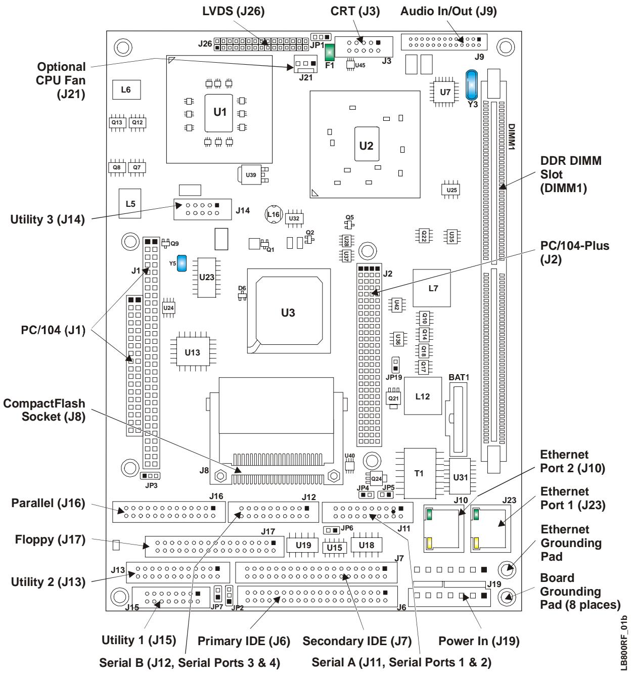
![LVDS (J26)\nCRT (J3)\nAudio In/Out (J9)\nOptional\nCPU Fan\n(J21)\nL6\nQ13 Q12\nU1\nF1 U45 J3\nJ21\nU2\nU7 Y3\nU39\nU25\nL5\nJ14\nL16 U32\nQ5\nQ1\nQ9\nY5\nU23\nU3\nJ1\nPC/104 (J1)\nCompactFlash\nSocket (J8)\nJP3\nJ8\nJ2\nL7\nQ10 Q11 Q12 Q13\nQ21\nJP19 L12 BAT1\nT1 U31\nJP4 JP5\nJ10 J23\nParallel (J16)\nFloppy (J17)\nUtility 2 (J13)\nJ13\nJ15 J16 J17 J18 J19\nJP7 JP2\nUtility 1 (J15) Primary IDE (J6) Secondary IDE (J7) Power In (J19)\nSerial B (J12, Serial Ports 3 & 4) Serial A (J11, Serial Ports 1 & 2)\nDDR DIMM\nSlot\n(DIMM1)\nPC/104-Plus\n(J2)\nEthernet Port 2 (J10)\nEthernet Port 1 (J23)\nEthernet Grounding Pad\nBoard Grounding Pad (8 places)\nLB800RF_01b](.littleboard800-manual-rev-a/a7ab6217baceac42f77c5d66caf4809fdb32a1d859f3c023bd680412af7ba754.jpg)

Figure 2-6. Connector Locations (Top view)

# CAUTION

The two Ethernet ports share a common ground (transformer center tap), that is floating until you determine how the common ground is connected. The grounding holes (8) of the LittleBoard 800 are connected to ground potential (return) of the DC power supply connected to the board through J19.

# NOTE

Pin-1 is shown as a black pin (square or round) in all connectors and jumpers in all illustrations.

# LED Definitions

Tables 2-3 and 2-4 provide the LED colors and definitions for the Ethernet ports, Port 1 (J23) and Port 2 (J10) located on the LittleBoard 800. Refer to Figure 2-6.

Table 2-3. Ethernet Port 1 (J23) LED Indicators

<table><tr><td>Indicator</td><td>Definition</td></tr><tr><td>&lt;img src="images/448e5c43f2f3bbd217083bfc172ab08bfd90e98c3fb3b5f04236c8676d0e82ec.jpg"/&gt;Ethernet/Link/Activity LED</td><td>Link/Activity LED – This yellow LED is the activity/link indicator and provides the status of Ethernet port 1 (J23).A steady On LED indicates a link is establishedA flashing LED indicates active data transfers</td></tr><tr><td>Ethernet Speed LED &lt;img src="images/e6ccc7354c9ae052747d5b11fb9b6033ac998a6e727bbb265ae9acbd61f14d5b.jpg"/&gt;</td><td>Speed LED – This green LED is the Speed indicator and indicates transmit or receive speed of Ethernet port 1 (J23).A steady Off LED shows the port at 10BaseT speedA steady On LED shows the port at 100BaseT speed</td></tr></table>

Table 2-4. Ethernet Port 2 (J10) LED Indicators

<table><tr><td>Indicator</td><td>Definition</td></tr><tr><td>&lt;img src="images/9a16eb773ae4dc84928a6eae9828c8aaedbaf5b3177791a124527043c5302fdd.jpg"/&gt;Ethernet /Link/Activity LED</td><td>Link/Activity LED – This yellow LED is the activity/link indicator and provides the status of Ethernet port 2 (J10).A steady On LED indicates a link is establishedA flashing LED indicates active data transfers</td></tr><tr><td>Ethernet Speed LED &lt;img src="images/9db0ef071cde8f124d923a8d2b924979fade0846147e715972604904ee2bfb27.jpg"/&gt;</td><td>Speed LED – This green LED is the Speed indicator and indicates transmit or receive speed of Ethernet port 2 (J10).A steady On LED indicates the port is at 10/100BaseT speedA steady Off LED indicates the port is at 1000BaseT speed</td></tr></table>

# Jumper Definitions

Table 2-5 describes the jumpers shown in Figure 2-7.

Table 2-5. Jumper Settings

<table><tr><td>Jumper #</td><td>Installed</td><td>Removed/Installed</td></tr><tr><td>JP1 – LVDS Voltage Select</td><td>Enable +3.3V (pins 1-2)</td><td>Enable +5V (pins 2-3)</td></tr><tr><td>JP2 – CompactFlash Master/Slave</td><td>Enable Master (pins 1-2)</td><td>Enable Slave (pins 2-3) Default</td></tr><tr><td>JP3 – CompactFlash Voltage Selection</td><td>Enable +5V (pins 1-2)</td><td>Enable +3.3V (pins 2-3)</td></tr><tr><td>JP4 – Serial Port 1 RS485 Termination</td><td>Enable Termination (pins 1-2)</td><td>Disable Termination (Removed) Default</td></tr><tr><td>JP5 – Serial Port 2 RS485 Termination</td><td>Enable Termination (pins 1-2)</td><td>Disable Termination (Removed) Default</td></tr><tr><td>JP6 – Serial Port 3 RS485 Termination</td><td>Enable Termination (pins 1-2)</td><td>Disable Termination (Removed) Default</td></tr><tr><td>JP7 – Serial Port 4 RS485 Termination</td><td>Enable Termination (pins 1-2)</td><td>Disable Termination (Removed) Default</td></tr><tr><td>JP19 – CMOS Normal/Clear</td><td>Clear CMOS (pins 1-2)</td><td>Normal (Removed) Default</td></tr></table>

<table><tr><td>Jumper #</td><td>Installed</td><td>Removed/Installed</td></tr><tr><td>JP1 – LVDS Voltage Select</td><td>Enable +3.3V (pins 1-2)</td><td>Enable +5V (pins 2-3)</td></tr><tr><td>JP2 – CompactFlash Master/Slave</td><td>Enable Master (pins 1-2)</td><td>Enable Slave (pins 2-3) Default</td></tr><tr><td>JP3 – CompactFlash Voltage Selection</td><td>Enable +5V (pins 1-2)</td><td>Enable +3.3V (pins 2-3)</td></tr><tr><td>JP4 – Serial Port 1 RS485 Termination</td><td>Enable Termination (pins 1-2)</td><td>Disable Termination (Removed) Default</td></tr><tr><td>JP5 – Serial Port 2 RS485 Termination</td><td>Enable Termination (pins 1-2)</td><td>Disable Termination (Removed) Default</td></tr><tr><td>JP6 – Serial Port 3 RS485 Termination</td><td>Enable Termination (pins 1-2)</td><td>Disable Termination (Removed) Default</td></tr><tr><td>JP7 – Serial Port 4 RS485 Termination</td><td>Enable Termination (pins 1-2)</td><td>Disable Termination (Removed) Default</td></tr><tr><td>JP19 – CMOS Normal/Clear</td><td>Clear CMOS (pins 1-2)</td><td>Normal (Removed) Default</td></tr></table>

Note: Only the jumpers listed above are populated on the board. Jumpers or shunts use 2mm spacing.

![LVDS Voltage Select (JP1)\nCRT Fuse (F1)\nCMOS\nNormal/Clear (JP19)\nSerial Port 1\nRS485\nTermination (JP4)\nSerial Port 2\nRS485\nTermination (JP5)\nSerial Port 3\nRS485\nTermination (JP6)\nCompactFlash\nVoltage (JP3)\nSerial Port 4 RS485\nTermination (JP7)\nCompactFlash\nMaster/Slave (JP2)\nLB800RF_01c](.littleboard800-manual-rev-a/2e662bff7d9f2497302913de6d8aa41665f367c4959fc99b74385d1cea837a5b.jpg)

Figure 2-7. Jumpers and Fuse Locations (Top view)

# Additional Components

The fuse in Table 2-6 is shown in Figure 2-7.

Table 2-6. Additional Component Descriptions

<table><tr><td>Component</td><td>Description</td></tr><tr><td>F1 (1.5A) Auto Reset</td><td>Overcurrent Fuse for the CRT on connector J3</td></tr></table>

# Specifications

# Physical Specifications

Table 2-7 gives the physical dimensions of the board and Figures 2-8 and 2-9 give the mounting dimensions and pin-1 connector locations.

Table 2-7. Weight and Footprint Dimensions

<table><tr><td>Item</td><td>Dimension</td><td rowspan="6">NOTE Overall height is measured from the upper board surface to the highest permanent component (battery in socket) on the upper board surface. This measurement does not include the various heatsinks or various size DIMMs inserted into the socket. The DIMMs or heatsinks could increase this dimension.</td></tr><tr><td>Weight</td><td>0.351kg. (0.775lbs.)</td></tr><tr><td>Height (overall)</td><td>24.94mm (0.982&quot;)</td></tr><tr><td>Width</td><td>146mm (5.75&quot;)</td></tr><tr><td>Length</td><td>203mm (8.0&quot;)</td></tr><tr><td>Thickness</td><td>2.36mm (0.093&quot;)</td></tr></table>

# Environmental Specifications

Table 2-8 provides the most efficient operating and storage condition ranges required for this board.

Table 2-8. Environmental Requirements

<table><tr><td></td><td>Parameter</td><td>600MHz Celeron M Conditions</td><td>1.0GHz Celeron M Conditions</td><td>1.4GHz Pentium M Conditions</td></tr><tr><td rowspan="3">Temperature</td><td>Operating</td><td>+0°to+70°C(32°to +158°F)</td><td>+0°to+70°C(32°to +158°F)</td><td>+0°to+70°C(32°to +158°F)</td></tr><tr><td>Extended(Optional)</td><td>-40°to+85°C(-40°to+185°F)</td><td>-40°to+85°C(-40°to+185°F)</td><td>-40°to+85°C*(-40°to+185°F)</td></tr><tr><td>Storage</td><td>-55°to+85°C(-67°to+185°F)</td><td>-55°to+85°C(-67°to+185°F)</td><td>-55°to+85°C(-67°to+185°F)</td></tr><tr><td rowspan="2">Humidity</td><td>Operating</td><td>5% to 95%relative humidity,non-condensing</td><td>5% to 95%relative humidity,non-condensing</td><td>5% to 95%relative humidity,non-condensing</td></tr><tr><td>Non-operating</td><td>5% to 95%relative humidity,non-condensing</td><td>5% to 95%relative humidity,non-condensing</td><td>5% to 95%relative humidity,non-condensing</td></tr></table>

Note: \*The 1.4GHz Pentium M requires a fan above $7 0 \mathrm { { } ^ { \circ } C } .$ .

# Power Specifications

Table 2-9 shows the power requirements from the baseboard and the board power output.

Table 2-9. Power Supply Requirements

<table><tr><td>Parameter</td><td>600MHz Celeron M Characteristics</td><td>1.0GHz Celeron M Characteristics</td><td>1.4GHz Pentium M Characteristics</td></tr><tr><td>Input Type</td><td>Regulated DC voltages</td><td>Regulated DC voltages</td><td>Regulated DC voltages</td></tr><tr><td>In-rush Current* (Typical)</td><td>11Amps</td><td>15Amps</td><td>10.2Amps</td></tr><tr><td>BIT** Current (Typical)</td><td>2.7A (13.5W)</td><td>2.8A (14W)</td><td>3.4A (17W)</td></tr></table>

Notes: \*In-rush measured with video, 128MB DDR PC2700 RAM memory, and power connected. \*\*The BIT (burn in test) current was measured using with 128MB DDR PC2700 RAM, video, Ampro I/O Interface board, floppy (1), IDE HDD (1), PS/2 keyboard & mouse, 4 Serial loopbacks, externally powered USB CD-ROM (1), externally powered USB HDD (1), USB Jump-Drive (1), USB CompactFlash reader with 64MB CompactFlash card (1), onboard 64MB CompactFlash card, and two operating Ethernet channels. LittleBoard 800 used Windows 2000 as OS.

# Thermal/Cooling Requirements

The CPU, Memory Hub, I/O Hub, and voltage regulators are the sources of heat on the board. The LittleBoard 800 is designed to operate at the maximum speed of the respective CPUs, 600MHz, 1.0GHz, or 1.4GHz. The Celeron M CPUs require a heatsink but no fan for – 40°to+85°C operation. The Pentium M CPU requires a heatsink but no fan for $+ 0 ^ { \circ } \mathrm { t o } + 7 0 ^ { \circ } \mathrm { C }$ operation, but does require a fan above +70°C (+70°C to+85°C operation).

# Mechanical Specifications

Figures 2-8 and 2-9 show top views of the LittleBoard 800 with the mechanical mounting dimensions.
![7.800\n7.600\n7.535\n7.225\n6.345\nJ23\nJ10\n5.700\n5.350\nBAT1\nJ6\nJ7\nJ11\nJ12\nJ17\nJ16\nJ8\nJ14\nJ15\nJ13\n7.600\n6.800\n6.350\n5.800\n3.500\n2.700\n2.650\n2.200\nDIMM1\nJ9\nJ3\nJ21\nJ26\n0.055\n0.0\nLB800RF_01d\n-0.200\n-0.100\n-0.200\n-0.200\n0.0\n0.575\n1.875\n4.025\n5.050\n5.250\n5.350\n5.550](.littleboard800-manual-rev-a/fd663f1b3a30cd97b5fc06ea30e477c52932dcff463b27232418c78334c88eb8.jpg)

Figure 2-8. LittleBoard 800 Dimensions (Top view, #1)

NOTE

All dimensions are given in inches.

![| Component | Value |\n| --------- | ----- |\n| J19       | 7.800 |\n| J6        | 7.600 |\n| J15       | 7.600 |\n| J13       | 7.500 |\n| J11       | 7.150 |\n| J17       | 7.150 |\n| J23       | 6.465 |\n| J10       | 5.700 |\n| J12       | 5.700 |\n| J16       | 5.700 |\n| BAT1      | 2.800 |\n| J2        | 2.800 |\n| J8        | 5.800 |\n| J1        | 2.650 |\n| DIMM1     | 0.0   |\n| J9        | -0.060|\n| J3        | -0.200|\n| J21       | 0.0   |\n| J26       | 0.0   |\nLB800RF_01e](.littleboard800-manual-rev-a/c6a7eade7bb72612fe83b341d404e571e557d722706c2ffbd667dab6d871b809.jpg)

Figure 2-9. LittleBoard 800 Dimensions (Top view, #2)

NOTE

All dimensions are given in inches.

# Overview

This chapter discusses the chips and features of the connectors in the following order:

• CPU (U1)
• Memory (DIMM1)
• PC/104-Plus (J2A, B, C, D)
• PC/104 (J1A, B, C, D)
• IDE Interfaces (J6, J7)
• CompactFlash Socket (J8)
• Floppy Interface (J17)
• Serial Interfaces (J11, J12)
• Parallel Interface (J16)
• Utility Interfaces (J13, J14, J15)
♦ Keyboard
♦ Mouse
♦ Battery
♦ Reset Switch
♦ Speaker
♦ USB ，
+ ♦ SMBus
♦ Infrared (IrDA)
• Ethernet Interfaces (J10, J23)
• Audio Interface (J5)
• Miscellaneous
♦ Time of Day/RTC
♦ Temperature Monitoring
♦ Serial Console
♦ Watchdog timer
• Power Interface (J19)

• CRT/LVDS Video Interfaces (J3, J4)

♦ Oops! Jumper (BIOS recovery)

# NOTE

Ampro Computers, Inc. only supports the features/options tested and listed in this manual. The main integrated circuits (chips) used in the LittleBoard 800 may provide more features or options than are listed for the LittleBoard 800, but some of these chip features/options are not supported on the board and may not function as specified in the chip documentation.

# CPU (U1)

The LittleBoard 800 offers high performance Intel processors at 1.4GHz Low Voltage (LV) Pentium® M 738, 1.0GHz Ultra Low Voltage (ULV) Celeron® M 373, or 600MHz Ultra Low Voltage (ULV) Celeron M processor.

# Celeron M Processors

The 600MHz Celeron M processor (Banias core) has 512kB L2 Cache on board, with a 400MHz FSB (front side bus). This Celeron M processor uses 130nm architecture and requires a heatsink, but no fan.

The 1.0GHz Celeron M processor (Dothan core) has 512kB L2 Cache on board with a 400MHz FSB. This Celeron M 373 processor uses 90nm architecture and requires a heatsink, but no fan.

# Pentium M Processor

The 1.4GHz Pentium M 738 processor (Dothan core) has 2MB L2 Cache on board with a 400MHz FSB. This Pentium M 738 processor uses 90nm architecture and requires a heatsink, but no fan below 70° C..

# Memory

The LittleBoard 800 memory consists of the following elements:

• DDR DIMM RAM
• Flash memory

# DDR DIMM Memory (DIMM1)

The LittleBoard 800 supports a single standard 184-pin DDR DIMM slot.

• DIMM slot can support up to 1GB of memory
• Supports PC2100 (266MHz) or PC2700 (333MHz) DDR RAM
• +2.5V SDRAM

# Flash Memory (U13)

There is an 8-bit wide, 512kB flash device used for system BIOS that is connected to the I/O Hub, 82801DBM (Southbridge), through the LPC bus. The BIOS is re-programmable and the supported features are detailed in Chapter 4, BIOS Setup.

# Interrupt Channel Assignments

The channel interrupt assignments are shown in Table 3-1.

Table 3-1. Interrupt Channel Assignments

<table><tr><td>Device vs IRQ No.</td><td>0</td><td>1</td><td>2</td><td>3</td><td>4</td><td>5</td><td>6</td><td>7</td><td>8</td><td>9</td><td>10</td><td>11</td><td>12</td><td>13</td><td>14</td><td>15</td></tr><tr><td>Timer</td><td>X</td><td></td><td></td><td></td><td></td><td></td><td></td><td></td><td></td><td></td><td></td><td></td><td></td><td></td><td></td><td></td></tr><tr><td>Keyboard</td><td></td><td>X</td><td></td><td></td><td></td><td></td><td></td><td></td><td></td><td></td><td></td><td></td><td></td><td></td><td></td><td></td></tr><tr><td>Secondary Cascade</td><td></td><td></td><td>X</td><td></td><td></td><td></td><td></td><td></td><td></td><td></td><td></td><td></td><td></td><td></td><td></td><td></td></tr><tr><td>COM1</td><td></td><td>O</td><td></td><td>O</td><td>D</td><td>O</td><td>O</td><td>O</td><td></td><td>O</td><td>O</td><td>O</td><td>O</td><td></td><td>O</td><td>O</td></tr><tr><td>COM2</td><td></td><td>O</td><td></td><td>D</td><td>O</td><td>O</td><td>O</td><td>O</td><td></td><td>O</td><td>O</td><td>O</td><td>O</td><td></td><td>O</td><td>O</td></tr><tr><td>COM3</td><td></td><td>O</td><td></td><td>O</td><td>O</td><td>O</td><td>O</td><td>O</td><td></td><td>O</td><td>O</td><td>D</td><td>O</td><td></td><td>O</td><td>O</td></tr><tr><td>COM4</td><td></td><td>O</td><td></td><td>O</td><td>O</td><td>O</td><td>O</td><td>O</td><td></td><td>O</td><td>D</td><td>O</td><td>O</td><td></td><td>O</td><td>O</td></tr><tr><td>Floppy</td><td></td><td></td><td></td><td></td><td></td><td></td><td>X</td><td></td><td></td><td></td><td></td><td></td><td></td><td></td><td></td><td></td></tr><tr><td>Parallel</td><td></td><td>O</td><td></td><td>O</td><td>O</td><td>O</td><td>O</td><td>D</td><td></td><td>O</td><td>O</td><td>O</td><td>O</td><td></td><td>O</td><td>O</td></tr><tr><td>RTC</td><td></td><td></td><td></td><td></td><td></td><td></td><td></td><td></td><td>X</td><td></td><td></td><td></td><td></td><td></td><td></td><td></td></tr><tr><td>IDE Primary</td><td></td><td></td><td></td><td></td><td></td><td></td><td></td><td></td><td></td><td></td><td></td><td></td><td></td><td></td><td>X</td><td></td></tr><tr><td>IDE Secondary</td><td></td><td></td><td></td><td></td><td></td><td></td><td></td><td></td><td></td><td></td><td></td><td></td><td></td><td></td><td></td><td>X</td></tr><tr><td>Math Coprocessor</td><td></td><td></td><td></td><td></td><td></td><td></td><td></td><td></td><td></td><td></td><td></td><td></td><td></td><td>X</td><td></td><td></td></tr><tr><td>PS/2 Mouse</td><td></td><td></td><td></td><td></td><td></td><td></td><td></td><td></td><td></td><td></td><td></td><td></td><td>X</td><td></td><td></td><td></td></tr><tr><td>PCI INTA</td><td></td><td>O</td><td></td><td>O</td><td>O</td><td>D</td><td>O</td><td>O</td><td></td><td>O</td><td>O</td><td>O</td><td>O</td><td></td><td>O</td><td>O</td></tr><tr><td>PCI INTB</td><td></td><td>O</td><td></td><td>O</td><td>O</td><td>O</td><td>O</td><td>O</td><td></td><td>D</td><td>O</td><td>O</td><td>O</td><td></td><td>O</td><td>O</td></tr><tr><td>PCI INTC</td><td></td><td>O</td><td></td><td>O</td><td>O</td><td>D</td><td>O</td><td>O</td><td></td><td>O</td><td>O</td><td>O</td><td>O</td><td></td><td>O</td><td>O</td></tr><tr><td>PCI INTD</td><td></td><td>O</td><td></td><td>O</td><td>O</td><td>O</td><td>O</td><td>O</td><td></td><td>D</td><td>O</td><td>O</td><td>O</td><td></td><td>O</td><td>O</td></tr><tr><td>PCI INTE</td><td></td><td>O</td><td></td><td>O</td><td>O</td><td>D</td><td>O</td><td>O</td><td></td><td>O</td><td>O</td><td>O</td><td>O</td><td></td><td>O</td><td>O</td></tr><tr><td>PCI INTF</td><td></td><td>O</td><td></td><td>O</td><td>O</td><td>O</td><td>O</td><td>O</td><td></td><td>D</td><td>O</td><td>O</td><td>O</td><td></td><td>O</td><td>O</td></tr><tr><td>PCI INTH</td><td></td><td>O</td><td></td><td>O</td><td>O</td><td>D</td><td>O</td><td>O</td><td></td><td>O</td><td>O</td><td>O</td><td>O</td><td></td><td>O</td><td>O</td></tr></table>

Legend: D = Default, O = Optional, X = Fixed

# NOTE

The IRQs for the Ethernet, Video, and Internal Local Bus (ISA) are automatically assigned by the BIOS Plug and Play logic. Local IRQs assigned during initialization can not be used by external devices.

# Memory Map

The following table provides the common PC/AT memory allocations. Memory below 000500h is used by the BIOS.

Table 3-2. Memory Map

<table><tr><td>Base Address</td><td>Function</td></tr><tr><td>00000000h - 0009FFFFh</td><td>Conventional Memory</td></tr><tr><td>000A0000h - 000AFFFFh</td><td>Graphics Memory</td></tr><tr><td>000B0000h - 000B7FFFh</td><td>Mono Text Memory</td></tr><tr><td>000B8000h - 000BFFFFh</td><td>Color Text Memory</td></tr><tr><td>000C0000h - 000C7FFFh</td><td>Standard Video BIOS</td></tr><tr><td>000F0000h - 000FFFFFFh</td><td>System BIOS Area (Storage and RAM Shadowing)</td></tr><tr><td>00100000h - 04000000h</td><td>Extended Memory (If onboard VGA is enabled, then the amount of memory assigned is subtracted from extended memory)</td></tr><tr><td>FFF80000h - FFFFFFFH</td><td>System Flash</td></tr></table>

# I/O Address Map

Table 3-3 shows the I/O address map.
Table 3-3. I/O Address Map

<table><tr><td>Address (hex)</td><td>Subsystem</td></tr><tr><td>000-00F</td><td>Primary DMA Controller</td></tr><tr><td>020-021</td><td>Master Interrupt Controller</td></tr><tr><td>040-043</td><td>Programmable Interrupt Timer (Clock/Timer)</td></tr><tr><td>060-06F</td><td>Keyboard Controller</td></tr><tr><td>070-07F</td><td>CMOS RAM, NMI Mask Reg, RT Clock</td></tr><tr><td>080-09F</td><td>DMA Page Registers</td></tr><tr><td>092</td><td>Fast A20 gate and CPU reset</td></tr><tr><td>094</td><td>Motherboard enable</td></tr><tr><td>102</td><td>Video subsystem register</td></tr><tr><td>0A0-0BF</td><td>Slave Interrupt Controller</td></tr><tr><td>0C0-0DF</td><td>Slave DMA Controller #2</td></tr><tr><td>0F0-0FF</td><td>Math Coprocessor</td></tr><tr><td>170-177</td><td>Secondary IDE Hard Disk Controller</td></tr><tr><td>1F0-1F8</td><td>Primary IDE Hard Disk Controller</td></tr><tr><td>278-27F</td><td>Parallel Printer</td></tr><tr><td>2E8-2FF</td><td>Serial Port 4 (COM4)</td></tr><tr><td>2F8-2FF</td><td>Serial Port 2 (COM2)</td></tr><tr><td>378-37F</td><td>Parallel port (Standard and EPP)</td></tr><tr><td>3C0-3DF</td><td>VGA</td></tr><tr><td>3E8-3EF</td><td>Serial Port 3 (COM3)</td></tr><tr><td>3F0-3F7</td><td>Floppy Disk Controller</td></tr><tr><td>3F8-3FF</td><td>Serial Port 1 (COM1)</td></tr><tr><td>778-77A</td><td>Parallel Port (ECP Extensions) (Port 378+400)</td></tr><tr><td>CF8-CFF</td><td>PCI bus Configuration Address and Data</td></tr></table>

# PC/104-Plus Interface (J2)

PC/104-Plus uses a 120 pin (4x30) 2mm connector interface. This interface connector carries all of the appropriate PCI signals operating at clock speeds up to 33MHz. The Memory Hub (82855GME), integrates a PCI arbiter that supports up to four devices with three external PCI masters. This interface header accepts stackable modules and is located on the top of the board.

Table 3-4 provides the signals and descriptions for the PCI bus pin-outs of 120 pins, 4 rows, consecutive numbering, (A1, B1, C1, D1), 2mm connector.

Notes: The shaded area denotes power or ground. The signals marked with \* = Negative true logic.
Table 3-4. PC/104-Plus Pin/Signal Descriptions (J2)

<table><tr><td>Pin #</td><td>Signal</td><td>Input/Output</td><td>Description</td></tr><tr><td>1 (A1)</td><td>Key/GND</td><td></td><td>Key – Ground</td></tr><tr><td>2 (A2)</td><td>VI/O</td><td></td><td>+5 volts ±5% (Reference voltage only)</td></tr><tr><td>3 (A3)</td><td>AD05</td><td>T/S</td><td>PCI Address/Data Bus Line 5 – These signals (AD31 - AD0) are multiplexed on these pins. A bus transaction consists of an address followed by one or more data cycles.</td></tr><tr><td>4 (A4)</td><td>C/BE0*</td><td>T/S</td><td>PCI Bus Command/Byte Enable 0 – These signals (C/BE 0 -3) are line multiplexed, so that during the address cycle, the command is defined and during the data cycle, the byte enable is defined.</td></tr><tr><td>5 (A5)</td><td>GND</td><td></td><td>Ground</td></tr><tr><td>6 (A6)</td><td>AD11</td><td>T/S</td><td>Address/Data Bus Line 11 – Refer to pin-A3 for more information.</td></tr><tr><td>7 (A7)</td><td>AD14</td><td>T/S</td><td>Address/Data Bus Line 14 – Refer to pin-A3 for more information.</td></tr><tr><td>8 (A8)</td><td>+3.3V</td><td></td><td>+3.3 volts ±5% power supply input</td></tr><tr><td>9 (A9)</td><td>SERR*</td><td>O/D</td><td>System Error – This signal is for reporting address parity errors.</td></tr><tr><td>10 (A10)</td><td>GND</td><td></td><td>Ground</td></tr><tr><td>11 (A11)</td><td>STOP*</td><td>S/T/S</td><td>Stop – This signal indicates the current selected device is requesting the master to stop the current transaction</td></tr><tr><td>12 (A12)</td><td>+3.3V</td><td></td><td>+3.3 volts ±5% power supply input</td></tr><tr><td>13 (A13)</td><td>FRAME*</td><td>S/T/S</td><td>Frame access – This signal is driven by the current master, indicating a transaction start and will remain active until the final data cycle.</td></tr><tr><td>14 (A14)</td><td>GND</td><td></td><td>Ground</td></tr><tr><td>15 (A15)</td><td>AD18</td><td>T/S</td><td>Address/Data Bus Line 18 – Refer to pin-A3 for more information.</td></tr><tr><td>16 (A16)</td><td>AD21</td><td>T/S</td><td>Address/Data Bus Line 21 – Refer to pin-A3 for more information.</td></tr><tr><td>17 (A17)</td><td>+3.3V</td><td></td><td>+3.3 volts ±5% power supply input</td></tr><tr><td>18 (A18)</td><td>IDSEL0</td><td>In</td><td>Initialization Device Select 0 – These signals (IDSEL 0-3) are used as the chip-selects during configuration read and write transactions.</td></tr><tr><td>19 (A19)</td><td>AD24</td><td>T/S</td><td>Address/Data Bus Line 24 – Refer to pin A3 for more information.</td></tr><tr><td>20 (A20)</td><td>GND</td><td></td><td>Ground</td></tr><tr><td>21 (A21)</td><td>AD29</td><td>T/S</td><td>Address/Data Bus Line 29 – Refer to pin A3 for more information.</td></tr><tr><td>22 (A22)</td><td>+5V</td><td></td><td>+5 volts ±5% power supply input</td></tr><tr><td>23 (A23)</td><td>REQ0*</td><td>T/S</td><td>Bus Request 0 – These signals (REQ 0-2) indicate to the arbitrator the device desires use of the bus.</td></tr><tr><td>24 (A24)</td><td>GND</td><td></td><td>Ground</td></tr><tr><td>25 (A25)</td><td>GNT1*</td><td>T/S</td><td>Grant 1 – These signal (GNT 0-2) lines indicate access has been granted to the requesting device (PCI Masters).</td></tr><tr><td>26 (A26)</td><td>+5V</td><td></td><td>+5 volts ±5% power supply input</td></tr><tr><td>27 (A27)</td><td>CLK2</td><td>In</td><td>Clock 2 – These clocks (CLK 0-3) provide timing outputs for four external PCI devices and all timing transactions on the PCI bus.</td></tr><tr><td>28 (A28)</td><td>GND</td><td></td><td>Ground</td></tr><tr><td>29 (A29)</td><td>+12V</td><td></td><td>+12 volts ±5% power supply input</td></tr><tr><td>30 (A30)</td><td>-12V</td><td></td><td>-12 volts (Supplied externally or through PC/104-Plus bus)</td></tr><tr><td>31 (B1)</td><td>NC</td><td></td><td>Not connected (Reset)</td></tr><tr><td>32 (B2)</td><td>AD02</td><td>T/S</td><td>Address/Data Bus Line 2 – Refer to pin A3 for more information.</td></tr><tr><td>33 (B3)</td><td>GND</td><td></td><td>Ground</td></tr><tr><td>34 (B4)</td><td>AD07</td><td>T/S</td><td>Address/Data Bus Line 7 – Refer to pin A3 for more information.</td></tr><tr><td>35 (B5)</td><td>AD09</td><td>T/S</td><td>Address/Data Bus Line 9 – Refer to pin A3 for more information.</td></tr><tr><td>36 (B6)</td><td>VI/O</td><td></td><td>+5 volts ±5% (Reference voltage only)</td></tr><tr><td>37 (B7)</td><td>AD13</td><td>T/S</td><td>Address/Data Bus Line 13 – Refer to pin-A3 for more information.</td></tr><tr><td>38 (B8)</td><td>C/BE1*</td><td>T/S</td><td>Command/Byte Enable 1 – Refer to pin-A4 for more information.</td></tr><tr><td>39 (B9)</td><td>GND</td><td></td><td>Ground</td></tr><tr><td>40 (B10)</td><td>PERR*</td><td></td><td>Parity Error – This signal is for reporting data parity errors.</td></tr><tr><td>41 (B11)</td><td>+3.3V</td><td></td><td>+3.3 volts ±5% power supply input</td></tr><tr><td>42 (B12)</td><td>TRDY*</td><td>S/T/S</td><td>Target Ready – This signal indicates the selected device's ability to complete the current cycle of transaction. Both IRDY* and TRDY* must be asserted to terminate a data cycle.</td></tr><tr><td>43 (B13)</td><td>GND</td><td></td><td>Ground</td></tr><tr><td>44 (B14)</td><td>AD16</td><td>T/S</td><td>Address/Data Bus Line 16 – Refer to pin-A3 for more information.</td></tr><tr><td>45 (B15)</td><td>+3.3V</td><td></td><td>+3.3 volts ±5% power supply input</td></tr><tr><td>46 (B16)</td><td>AD20</td><td>T/S</td><td>Address/Data Bus Line 20 – Refer to pin-A3 for more information.</td></tr><tr><td>47 (B17)</td><td>AD23</td><td>T/S</td><td>Address/Data Bus Line 23 – Refer to pin-A3 for more information.</td></tr><tr><td>48 (B18)</td><td>GND</td><td></td><td>Ground</td></tr><tr><td>49 (B19)</td><td>C/BE3*</td><td>T/S</td><td>Command/Byte Enable 3 – Refer to pin-A4 for more information.</td></tr><tr><td>50 (B20)</td><td>AD26</td><td>T/S</td><td>Address/Data Bus Line 26 – Refer to pin-A3 for more information.</td></tr><tr><td>51 (B21)</td><td>+5V</td><td></td><td>+5 volts ±5% power supply input</td></tr><tr><td>52 (B22)</td><td>AD30</td><td>T/S</td><td>Address/Data Bus Line 30 – Refer to pin-A3 for more information.</td></tr><tr><td>53 (B23)</td><td>GND</td><td></td><td>Ground</td></tr><tr><td>54 (B24)</td><td>REQ2*</td><td>T/S</td><td>Bus Request 2 – Refer to pin-A23 for more information.</td></tr><tr><td>55 (B25)</td><td>VI/O</td><td></td><td>+5 volts ±5% (Reference voltage only)</td></tr><tr><td>56 (B26)</td><td>CLK0</td><td>In</td><td>Clock 0 – Refer to pin-A27 for more information</td></tr><tr><td>57 (B27)</td><td>+5V</td><td></td><td>+5 volts ±5% power supply input</td></tr><tr><td>58 (B28)</td><td>INTD*</td><td>O/D</td><td>Interrupt D – This signal is used to request interrupts only for multi-function devices.</td></tr><tr><td>59 (B29)</td><td>INTA*</td><td>O/D</td><td>Interrupt A – This signal is used to request an interrupt.</td></tr><tr><td>60 (B30)</td><td>REQ3*</td><td>T/S</td><td>Bus Request 3 – Refer to pin-A23 for more information.</td></tr><tr><td>61 (C1)</td><td>+5V</td><td></td><td>+5 volts ±5% power supply input</td></tr><tr><td>62 (C2)</td><td>AD01</td><td>T/S</td><td>Address/Data Bus Line 1 – Refer to pin-A3 for more information.</td></tr><tr><td>63 (C3)</td><td>AD04</td><td>T/S</td><td>Address/Data Bus Lines 4 – Refer to pin-A3 for more information.</td></tr><tr><td>64 (C4)</td><td>GND</td><td></td><td>Ground</td></tr><tr><td>65 (C5)</td><td>AD08</td><td>T/S</td><td>Address/Data Bus Line 8 – Refer to pin-A3 for more information.</td></tr><tr><td>66 (C6)</td><td>AD10</td><td>T/S</td><td>Address/Data Bus Line 10 – Refer to pin-A3 for more information.</td></tr><tr><td>67 (C7)</td><td>GND</td><td></td><td>Ground</td></tr><tr><td>68 (C8)</td><td>AD15</td><td>T/S</td><td>Address/Data Bus Line 15 – Refer to pin-A3 for more information.</td></tr><tr><td>69 (C9)</td><td>NC</td><td></td><td>Not connected (Snoop Backoff)</td></tr><tr><td>70 (C10)</td><td>+3.3V</td><td></td><td>+3.3 volts ±5% power supply input</td></tr><tr><td>71 (C11)</td><td>LOCK*</td><td>S/T/S</td><td>Lock – This signal indicates an operation that may require multiple transactions to complete</td></tr><tr><td>72 (C12)</td><td>GND</td><td></td><td>Ground</td></tr><tr><td>73 (C13)</td><td>IRDY*</td><td>S/T/S</td><td>Initiator Ready – This signal indicates the master’s ability to complete the current data cycle of the transaction</td></tr><tr><td>74 (C14)</td><td>+3.3V</td><td></td><td>+3.3 volts ±5% power supply input</td></tr><tr><td>75 (C15)</td><td>AD17</td><td>T/S</td><td>Address/Data Bus Line 17 – Refer to pin-A3 for more information.</td></tr><tr><td>76 (C16)</td><td>GND</td><td></td><td>Ground</td></tr><tr><td>77 (C17)</td><td>AD22</td><td>T/S</td><td>Address/Data Bus Line 22 – Refer to pin-A3 for more information.</td></tr><tr><td>78 (C18)</td><td>IDSEL1</td><td></td><td>Initialization Device Select 1 – Refer to pin-A18 for more information</td></tr><tr><td>79 (C19)</td><td>VI/O</td><td></td><td>+5 volts ±5% (Reference voltage only)</td></tr><tr><td>80 (C20)</td><td>AD25</td><td>T/S</td><td>Address/Data Bus Line 25 – Refer to pin-A3 for more information.</td></tr><tr><td>81 (C21)</td><td>AD28</td><td>T/S</td><td>Address/Data Bus Line 28 – Refer to pin-A3 for more information.</td></tr><tr><td>82 (C22)</td><td>GND</td><td></td><td>Ground</td></tr><tr><td>83 (C23)</td><td>REQ1*</td><td>T/S</td><td>Bus Request 1 – Refer to pin-A23 for more information.</td></tr><tr><td>84 (C24)</td><td>+5V</td><td></td><td>+5 volts ±5% power supply input</td></tr><tr><td>85 (C25)</td><td>GNT2*</td><td>T/S</td><td>Grant 2 – Refer to pin-A25 for more information</td></tr><tr><td>86 (C26)</td><td>GND</td><td></td><td>Ground</td></tr><tr><td>87 (C27)</td><td>CLK3</td><td>In</td><td>Clock 3 – Refer to pin-A27 for more information</td></tr><tr><td>88 (C28)</td><td>+5V</td><td></td><td>+5 volts ±5% power supply input</td></tr><tr><td>89 (C29)</td><td>INTB*</td><td>O/D</td><td>Interrupt B – This signal is used to request interrupts only for multi-function devices.</td></tr><tr><td>90 (C30)</td><td>GNT3*</td><td>T/S</td><td>Grant 3 – Refer to pin-A25 for more information</td></tr><tr><td>91 (D1)</td><td>AD00</td><td>T/S</td><td>Address/Data Bus Line 0 – Refer to pin-A3 for more information.</td></tr><tr><td>92 (D2)</td><td>+5V</td><td></td><td>+5 volts ±5% power supply input</td></tr><tr><td>93 (D3)</td><td>AD03</td><td>T/S</td><td>Address/Data Bus Line 3 – Refer to pin-A3 for more information.</td></tr><tr><td>94 (D4)</td><td>AD06</td><td>T/S</td><td>Address/Data Bus Line 6 – Refer to pin-A3 for more information.</td></tr><tr><td>95 (D5)</td><td>GND</td><td></td><td>Ground</td></tr><tr><td>96 (D6)</td><td>M66EN</td><td></td><td>Not supported – Reserved for 66MHz on PCI bus.</td></tr><tr><td>97 (D7)</td><td>AD12</td><td>T/S</td><td>Address/Data Bus Line 12 – Refer to pin-A3 for more information.</td></tr><tr><td>98 (D8)</td><td>+3.3V</td><td></td><td>+3.3 volts ±5% power supply input</td></tr><tr><td>99 (D9)</td><td>PAR</td><td>T/S</td><td>Bus Parity bit – This signal is the even parity bit on AD[31:0] and C/BE[3:0]*</td></tr><tr><td>100 (D10)</td><td>NC</td><td></td><td>Not connected (Snoop Done)</td></tr><tr><td>101 (D11)</td><td>GND</td><td></td><td>Ground</td></tr><tr><td>102 (D12)</td><td>DEVSEL*</td><td>S/T/S</td><td>Device Select – This signal is driven by the target device when its address is decoded.</td></tr><tr><td>103 (D13)</td><td>+3.3V</td><td></td><td>+3.3 volts ±5% power supply input</td></tr><tr><td>104 (D14)</td><td>C/BE2*</td><td></td><td>Command/Byte Enable 2 – Refer to pin-A4 for more information.</td></tr><tr><td>105 (D15)</td><td>GND</td><td></td><td>Ground</td></tr><tr><td>106 (D16)</td><td>AD19</td><td>T/S</td><td>Address/Data Bus Line 19 – Refer to pin-A3 for more information.</td></tr><tr><td>107 (D17)</td><td>+3.3V</td><td></td><td>+3.3 volts ±5% power supply input</td></tr><tr><td>108 (D18)</td><td>IDSEL2</td><td></td><td>Initialization Device Select 2 – Refer to pin-A18 for more info.</td></tr><tr><td>109 (D19)</td><td>IDSEL3</td><td></td><td>Initialization Device Select 3 – Refer to pin-A18 for more info.</td></tr><tr><td>110 (D20)</td><td>GND</td><td></td><td>Ground</td></tr><tr><td>111 (D21)</td><td>AD27</td><td>T/S</td><td>Address/Data Bus Line 27 – Refer to pin-A3 for more information.</td></tr><tr><td>112 (D22)</td><td>AD31</td><td>T/S</td><td>Address/Data Bus Line 31 – Refer to pin-A3 for more information.</td></tr><tr><td>113 (D23)</td><td>VI/O</td><td></td><td>+5 volts ±5% (Reference voltage only)</td></tr><tr><td>114 (D24)</td><td>GNT0*</td><td>T/S</td><td>Grant 0 – Refer to pin-A25 for more information.</td></tr><tr><td>115 (D25)</td><td>GND</td><td></td><td>Ground</td></tr><tr><td>116 (D26)</td><td>CLK1</td><td>In</td><td>Clock 1 – Refer to pin-A27 for more information.</td></tr><tr><td>117 (D27)</td><td>GND</td><td></td><td>Ground</td></tr><tr><td>118 (D28)</td><td>RST*</td><td>In</td><td>PCI bus reset – This signal is an output signal to reset the entire PCI Bus. This signal will be asserted during system reset.</td></tr><tr><td>119 (D29)</td><td>INTC*</td><td>O/D</td><td>Interrupt C – This signal is used to request interrupts only for multi-function devices.</td></tr><tr><td>120 (D30)</td><td>GND</td><td></td><td>Ground</td></tr></table>

The Input/Output signals in this table refer to the input/output signals listed in the PCI Local Bus Manual, Revision 2.2, Chapter 2, paragraph 2.1, Signal definitions. The following terms or acronyms are used in this table:

• In – Input is standard input only signal
• Out – Totem Pole output is a standard active driver
• T/S – Tri-State is a bi-directional input output pin
• S/T/S – Sustained Tri-State is an active low tri-state signal driven by one and only one agent at a time
• O/D – Open Drain allows multiple devices to share as a wire-OR.

# PC/104 Interface (J1A,B,C,D)

The PC/104 Bus uses a 104-pin 100 mil header interface. This interface header will carry all of the appropriate PC/104 signals operating at clock speeds up to 8MHz. This interface header accepts stackable modules and is located on the top of the board. The PC/104 connector uses 104-pin, 4 rows, consecutive numbering, (A1, B1, C0, D0), and 0.100" pin spacing.

Notes: The shaded area denotes power or ground. The signals marked with \* = Negative true logic.
Table 3-5. PC/104 Interface Pin/Signal Descriptions (J1A)

<table><tr><td>Pin #</td><td>Signal</td><td>Description (J1 Row A)</td></tr><tr><td>1 (A1)</td><td>IOCHCHK*</td><td>I/O Channel Check – This signal may be activated by ISA boards to request that a non-maskable interrupt (NMI) be generated to the system processor. It is driven active to indicate an uncorrectable error has been detected.</td></tr><tr><td>2 (A2)</td><td>SD7</td><td>System Data 7 – This signal (0 to 19) provides a system data bit.</td></tr><tr><td>3 (A3)</td><td>SD6</td><td>System Data 6 – Refer to pin-A2 for more information.</td></tr><tr><td>4 (A4)</td><td>SD5</td><td>System Data 5 – Refer to pin-A2 for more information.</td></tr><tr><td>5 (A5)</td><td>SD4</td><td>System Data 4 – Refer to pin-A2 for more information.</td></tr><tr><td>6 (A6)</td><td>SD3</td><td>System Data 3 – Refer to pin-A2 for more information.</td></tr><tr><td>7 (A7)</td><td>SD2</td><td>System Data 2 – Refer to pin-A2 for more information.</td></tr><tr><td>8 (A8)</td><td>SD1</td><td>System Data 1 – Refer to pin-A2 for more information.</td></tr><tr><td>9 (A9)</td><td>SD0</td><td>System Data 0 – Refer to pin-A2 for more information.</td></tr><tr><td>10 (A10)</td><td>IOCHRDY</td><td>I/O Channel Ready – This signal allows slower ISA boards to lengthen I/O or memory cycles by inserting wait states. This signal’s normal state is active high (ready). ISA boards drive the signal inactive low (not ready) to insert wait states. Devices using this signal to insert wait states should drive it low immediately after detecting a valid address decode and an active read, or write command. The signal is released high when the device is ready to complete the cycle.</td></tr><tr><td>11 (A11)</td><td>AEN</td><td>Address Enable – This signal is used to degate the system processor and other devices from the bus during DMA transfers. When this signal is active, the system DMA controller has control of the address, data, and read/write signals. This signal should be included as part of ISA board select decodes to prevent incorrect board selects during DMA cycles.</td></tr><tr><td>12 (A12)</td><td>SA19</td><td>System Address 19 – This signal (0 to 19) provides a system address bit.</td></tr><tr><td>13 (A13)</td><td>SA18</td><td>System Address 18 – Refer to pin-A12 , for more information.</td></tr><tr><td>14 (A14)</td><td>SA17</td><td>System Address 17 – Refer to pin-A12 , for more information.</td></tr><tr><td>15 (A15)</td><td>SA16</td><td>System Address 16 – Refer to pin-A12 , for more information.</td></tr><tr><td>16 (A16)</td><td>SA15</td><td>System Address 15 – Refer to pin-A12 , for more information.</td></tr><tr><td>17 (A17)</td><td>SA14</td><td>System Address 14 – Refer to pin-A12 , for more information.</td></tr><tr><td>18 (A18)</td><td>SA13</td><td>System Address 13 – Refer to pin-A12 , for more information.</td></tr><tr><td>19 (A19)</td><td>SA12</td><td>System Address 12 – Refer to pin-A12 , for more information.</td></tr><tr><td>20 (A20)</td><td>SA11</td><td>System Address 11 – Refer to pin-A12 , for more information.</td></tr><tr><td>21 (A21)</td><td>SA10</td><td>System Address 10 – Refer to pin-A12 , for more information.</td></tr><tr><td>22 (A22)</td><td>SA9</td><td>System Address 9 – Refer to pin-A12 , for more information.</td></tr><tr><td>23 (A23)</td><td>SA8</td><td>System Address 8 – Refer to pin-A12 , for more information.</td></tr><tr><td>24 (A24)</td><td>SA7</td><td>System Address 7 – Refer to pin-A12 , for more information.</td></tr><tr><td>25 (A25)</td><td>SA6</td><td>System Address 6 – Refer to pin-A12 , for more information.</td></tr><tr><td>26 (A26)</td><td>SA5</td><td>System Address 5 – Refer to pin-A12 , for more information.</td></tr><tr><td>27 (A27)</td><td>SA4</td><td>System Address 4 – Refer to pin-A12 , for more information.</td></tr><tr><td>28 (A28)</td><td>SA3</td><td>System Address 3 – Refer to pin-A12 , for more information.</td></tr><tr><td>29 (A29)</td><td>SA2</td><td>System Address 2 – Refer to pin-A12 , for more information.</td></tr><tr><td>30 (A30)</td><td>SA1</td><td>System Address 1 – Refer to pin-A12 , for more information.</td></tr><tr><td>31 (A31)</td><td>SA0</td><td>System Address 0 – Refer to pin-A12 , for more information.</td></tr><tr><td>32 (A32)</td><td>GND</td><td>Ground</td></tr></table>

Notes: The shaded area denotes power or ground. The signals marked with \* = Negative true logic.
Table 3-6. PC/104 Interface Pin/Signal Descriptions (J1B)

<table><tr><td>Pin #</td><td>Signal</td><td>Descriptions (J1 Row B)</td></tr><tr><td>33 (B1)</td><td>GND</td><td>Ground</td></tr><tr><td>34 (B2)</td><td>RSTDRV</td><td>Reset Drive – This signal is used to reset or initialize system logic on power up or subsequent system reset.</td></tr><tr><td>35 (B3)</td><td>+5V</td><td>+5 volts ±5% power supply input</td></tr><tr><td>36 (B4)</td><td>IRQ9</td><td>Interrupt Request 9 – Asserted by a device when it has a pending interrupt request. Only one device may use this request line at a time.</td></tr><tr><td>37 (B5)</td><td>-5V</td><td>-5V volt power (Supplied externally or through PC/104 bus)</td></tr><tr><td>38 (B6)</td><td>DRQ2</td><td>DMA Request 2 – Used by I/O resources to request DMA service, or to request ownership of the bus as a bus master device. Must be held high until associated DACK2 line is active.</td></tr><tr><td>39 (B7)</td><td>-12V</td><td>-12 volt power (Supplied externally or through PC/104 bus)</td></tr><tr><td>40 (B8)</td><td>ZWS</td><td>Zero Wait State – This signal is driven low by a bus slave device to indicate it is capable of performing a bus cycle without inserting any additional wait states. To perform a 16-bit memory cycle without wait states, this signal is derived from an address decode.</td></tr><tr><td>41 (B9)</td><td>+12V</td><td>+12 volt power supply input (Supplied externally or through PC/104 bus)</td></tr><tr><td>42 (B10)</td><td>NC</td><td>Not connected</td></tr><tr><td>43 (B11)</td><td>SMEMW*</td><td>System Memory Write – This signal is used by bus owner to request a memory device to store data currently on the data bus and only active for the lower 1MB. Used for legacy compatibility with 8-bit cards.</td></tr><tr><td>44 (B12)</td><td>SMEMR*</td><td>System Memory Read – This signal is used by bus owner to request a memory device to drive data onto the data bus and only active for lower 1MB. Used for legacy compatibility with 8-bit cards.</td></tr><tr><td>45 (B13)</td><td>IOW*</td><td>I/O Write – This strobe signal is driven by the owner of the bus (ISA bus master or DMA controller) and instructs the selected I/O device to capture the write data on the data bus.</td></tr><tr><td>46 (B14)</td><td>IOR*</td><td>I/O Read – This strobe signal is driven by the owner of the bus (ISA bus master or DMA controller) and instructs the selected I/O device to drive read data onto the data bus.</td></tr><tr><td>47 (B15)</td><td>DACK3*</td><td>DMA Acknowledge 3 – Used by DMA controller to select the I/O resource requesting the bus, or to request ownership of the bus as a bus master device. Can also be used by the ISA bus master to gain control of the bus from the DMA controller.</td></tr><tr><td>48 (B16)</td><td>DRQ3</td><td>DMA Request 3 – Used by I/O resources to request DMA service. Must be held high until associated DACK3 line is active.</td></tr><tr><td>49 (B17)</td><td>DACK1*</td><td>DMA Acknowledge 1 – Used by DMA controller to select the I/O resource requesting the bus, or to request ownership of the bus as a bus master device. Can also be used by the ISA bus master to gain control of the bus from the DMA controller.</td></tr><tr><td>50 (B18)</td><td>DRQ1</td><td>DMA Request 1 – Used by I/O resources to request DMA service. Must be held high until associated DACK1 line is active.</td></tr><tr><td>51 (B19)</td><td>REFRESH*</td><td>Memory Refresh – This signal is driven low to indicate a memory refresh cycle is in progress. Memory is refreshed every 15.6 usec.</td></tr><tr><td>52 (B20)</td><td>SYSCLK</td><td>System Clock – This is a free running clock typically in the 8MHz to 10MHz range, although its exact frequency is not guaranteed.</td></tr><tr><td>53 (B21)</td><td>IRQ7</td><td>Interrupt Request 7 – Asserted by a device when it has pending interrupt request. Only one device may use this request line at a time.</td></tr><tr><td>54 (B22)</td><td>IRQ6</td><td>Interrupt Request 6 – Asserted by a device when it has pending interrupt request. Only one device may use this request line at a time.</td></tr><tr><td>55 (B23)</td><td>IRQ5</td><td>Interrupt Request 5 – Asserted by a device when it has pending interrupt request. Only one device may use this request line at a time.</td></tr><tr><td>56 (B24)</td><td>IRQ4</td><td>Interrupt Request 4 – Asserted by a device when it has pending interrupt request. Only one device may use this request line at a time.</td></tr><tr><td>57 (B25)</td><td>IRQ3</td><td>Interrupt Request 3 – Asserted by a device when it has pending interrupt request. Only one device may use this request line at a time.</td></tr><tr><td>58 (B26)</td><td>DACK2*</td><td>DMA Acknowledge 2 – Used by DMA controller to select the I/O resource requesting the bus, or to request ownership of the bus as a bus master device. Can also be used by the ISA bus master to gain control of the bus from the DMA controller.</td></tr><tr><td>59 (B27)</td><td>TC</td><td>Terminal Count – This signal is a pulse to indicate a terminal count has been reached on a DMA channel operation.</td></tr><tr><td>60 (B28)</td><td>BALE</td><td>Buffered Address Latch Enable – This signal is used to latch the LA23 to LA17 signals or decodes of these signals. Addresses are latched on the falling edge of BALE. It is forced high during DMA cycles. When used with AENx, it indicates a valid processor or DMA address.</td></tr><tr><td>61 (B29)</td><td>+5V</td><td>+5 volts ±5% power supply input</td></tr><tr><td>62 (B30)</td><td>OSC</td><td>Oscillator – This clock signal operates at 14.3MHz. This signal is not synchronous with the system clock (SYSCLK).</td></tr><tr><td>63 (B31)</td><td>GND</td><td>Ground</td></tr><tr><td>64 (B32)</td><td>GND</td><td>Ground</td></tr></table>

Notes: The shaded area denotes power or ground. The signals marked with \* = Negative true logic.
Table 3-7. PC/104 Interface Pin/Signal Descriptions (J1C)

<table><tr><td>Pin #</td><td>Signal</td><td>Descriptions (J1 Row C)</td></tr><tr><td>1 (C0)</td><td>GND</td><td>Ground</td></tr><tr><td>2 (C1)</td><td>SBHE*</td><td>System Byte High Enable – This signal is driven low to indicate a transfer of data on the high half of the data bus (D15 to D8).</td></tr><tr><td>3 (C2)</td><td>LA23</td><td>Latchable Address 23 – This signal must be latched by the resource if the line is required for the entire data cycle.</td></tr><tr><td>4 (C3)</td><td>LA22</td><td>Latchable Address 22 – Refer to pin-C2, for more information.</td></tr><tr><td>5 (C4)</td><td>LA21</td><td>Latchable Address 21 – Refer to pin-C2, for more information.</td></tr><tr><td>6 (C5)</td><td>LA20</td><td>Latchable Address 20 – Refer to pin-C2, for more information.</td></tr><tr><td>7 (C6)</td><td>LA19</td><td>Latchable Address 19 – Refer to pin-C2, for more information.</td></tr><tr><td>8 (C7)</td><td>LA18</td><td>Latchable Address 18 – Refer to pin-C2, for more information.</td></tr><tr><td>9 (C8)</td><td>LA17</td><td>Latchable Address 17 – Refer to pin-C2, for more information.</td></tr><tr><td>10 (C9)</td><td>MEMR*</td><td>Memory Read – This signal instructs a selected memory device to drive data onto the data bus. It is active on all memory read cycles.</td></tr><tr><td>11 (C10)</td><td>MEMW*</td><td>Memory Write – This signal instructs a selected memory device to store data currently on the data bus. It is active on all memory write cycles.</td></tr><tr><td>12 (C11)</td><td>SD8</td><td>System Data 8 – Refer to pin-A2 for more information.</td></tr><tr><td>13 (C12)</td><td>SD9</td><td>System Data 9 – Refer to pin-A2 for more information.</td></tr><tr><td>14 (C13)</td><td>SD10</td><td>System Data 10 – Refer to pin-A2 for more information.</td></tr><tr><td>15 (C14)</td><td>SD11</td><td>System Data 11 – Refer to pin-A2 for more information.</td></tr><tr><td>16 (C15)</td><td>SD12</td><td>System Data 12 – Refer to pin-A2 for more information.</td></tr><tr><td>17 (C16)</td><td>SD13</td><td>System Data 13 – Refer to pin-A2 for more information.</td></tr><tr><td>18 (C17)</td><td>SD14</td><td>System Data 14 – Refer to pin-A2 for more information.</td></tr><tr><td>19 (C18)</td><td>SD15</td><td>System Data 15 – Refer to pin-A2 for more information.</td></tr><tr><td>20 (C19)</td><td>NC</td><td>Not connected</td></tr></table>

Notes: The shaded area denotes power or ground. The signals marked with \* = Negative true logic.
Table 3-8. PC/104 Interface Pin/Signal Descriptions (J1D)

<table><tr><td>Pin #</td><td>Signal</td><td>Descriptions (J1 Row D)</td></tr><tr><td>21 (D0)</td><td>GND</td><td>Ground</td></tr><tr><td>22 (D1)</td><td>MEMCS16*</td><td>Memory Chip Select 16 – This is signal is driven low by a memory slave device to indicates it is cable of performing a 16-bit memory data transfer. This signal is driven from a decode of the LA23 to LA17 address lines.</td></tr><tr><td>23 (D2)</td><td>IOCS16*</td><td>I/O Chip Select 16 – This signal is driven low by an I/O slave device to indicate it is capable of performing a 16-bit I/O data transfer. This signal is driven from a decode of the SA15 to SA0 address lines.</td></tr><tr><td>24 (D3)</td><td>IRQ10</td><td>Interrupt Request 10 – Asserted by a device when it has pending interrupt request. Only one device may use this request line at a time.</td></tr><tr><td>25 (D4)</td><td>IRQ11</td><td>Interrupt Request 11 – Asserted by a device when it has pending interrupt request. Only one device may use this request line at a time.</td></tr><tr><td>26 (D5)</td><td>IRQ12</td><td>Interrupt Request 12 – Asserted by a device when it has pending interrupt request. Only one device may use this request line at a time.</td></tr><tr><td>27 (D6)</td><td>IRQ15</td><td>Interrupt Request 15 – Asserted by a device when it has pending interrupt request. Only one device may use this request line at a time.</td></tr><tr><td>28 (D7)</td><td>IRQ14</td><td>Interrupt Request 14 – Asserted by a device when it has pending interrupt request. Only one device may use this request line at a time.</td></tr><tr><td>29 (D8)</td><td>DACK0*</td><td>DMA Acknowledge 0 – Used by DMA controller to select the I/O resource requesting the bus, or to request ownership of the bus as a bus master device. Can also be used by the ISA bus master to gain control of the bus from the DMA controller.</td></tr><tr><td>30 (D9)</td><td>DRQ0</td><td>DMA Request 0 – Used by I/O resources to request DMA service. Must be held high until associated DACK0 line is active.</td></tr><tr><td>31 (D10)</td><td>DACK5*</td><td>DMA Acknowledge 5 – Used by DMA controller to select the I/O resource requesting the bus, or to request ownership of the bus as a bus master device. Can also be used by the ISA bus master to gain control of the bus from the DMA controller.</td></tr><tr><td>32 (D11)</td><td>DRQ5</td><td>DMA Request 5 – Used by I/O resources to request DMA service. Must be held high until associated DACK5 line is active.</td></tr><tr><td>33 (D12)</td><td>DACK6*</td><td>DMA Acknowledge 6 – Used by DMA controller to select the I/O resource requesting the bus, or to request ownership of the bus as a bus master device. Can also be used by the ISA bus master to gain control of the bus from the DMA controller.</td></tr><tr><td>34 (D13)</td><td>DRQ6</td><td>DMA Request 6 – Used by I/O resources to request DMA service. Must be held high until associated DACK6 line is active.</td></tr><tr><td>35 (D14)</td><td>DACK7*</td><td>DMA Acknowledge 7 – Used by DMA controller to select the I/O resource requesting the bus, or to request ownership of the bus as a bus master device. Can also be used by the ISA bus master to gain control of the bus from the DMA controller.</td></tr><tr><td>36 (D15)</td><td>DRQ7</td><td>DMA Request 7 – Used by I/O resources to request DMA service. Must be held high until associated DACK7 line is active.</td></tr><tr><td>37 (D16)</td><td>+5V</td><td>+5 volts ±5% power supply</td></tr><tr><td>38 (D17)</td><td>MASTER*</td><td>Bus Master Assert – This signal is used by an ISA board along with a DRQ line to gain ownership of the ISA bus. Upon receiving a -DACK a device can pull -MASTER low which will allow it to control the system address, data, and control lines. After -MASTER is low, the device should wait one CLK period before driving the address and data lines, and two clock periods before issuing a read or write command.</td></tr><tr><td>39 (D18)</td><td>GND</td><td>Ground</td></tr><tr><td>40 (D19)</td><td>GND</td><td>Ground</td></tr></table>

# IDE Interface (J6, J7)

The LittleBoard 800 provides two IDE connectors for primary and secondary IDE signals.

The EIDE interface logic supports the following features:

• Bus master IDE transfer rate up to 100Mbps when 80-pin grounded shielded cable is used
• Increase reliability using Ultra DMA 33/66/100 transfer protocols
• Full scatter-gather capability
• Supports ATAPI and DVD compliant devices
• PIO IDE transfers as fast as 14Mbps.
• Single Bus Master EIDE
• Supports two IDE drives per interface (primary or secondary)

Notes: The shaded area denotes power or ground. The signals marked with \* = Negative true logic.
Tables 3-9 and 3-10 lists the signals for the two IDE 40 pin connectors, with 2 rows, odd/even, (1, 2), 0.100” pin spacing.
Table 3-9. Primary IDE Interface Pin/Signal Descriptions (J6)

<table><tr><td>Pin #</td><td>Signal</td><td>Description</td></tr><tr><td>1</td><td>RESET*</td><td>Low active hardware reset (RSTDRV inverted)</td></tr><tr><td>2</td><td>GND</td><td>Ground</td></tr><tr><td>3</td><td>PD7</td><td>Primary Disk Data 7 – These signals (0 to 15) provide the disk data signals.</td></tr><tr><td>4</td><td>PD8</td><td>Primary Disk Data 8 – These signals (0 to 15) provide the disk data signals.</td></tr><tr><td>5</td><td>PD6</td><td>Primary Disk Data 6 – These signals (0 to 15) provide the disk data signals.</td></tr><tr><td>6</td><td>PD9</td><td>Primary Disk Data 9 – These signals (0 to 15) provide the disk data signals.</td></tr><tr><td>7</td><td>PD5</td><td>Primary Disk Data 5 – These signals (0 to 15) provide the disk data signals.</td></tr><tr><td>8</td><td>PD10</td><td>Primary Disk Data 10 – These signals (0 to 15) provide the disk data signals.</td></tr><tr><td>9</td><td>PD4</td><td>Primary Disk Data 4 – These signals (0 to 15) provide the disk data signals.</td></tr><tr><td>10</td><td>PD11</td><td>Primary Disk Data 11 – These signals (0 to 15) provide the disk data signals.</td></tr><tr><td>11</td><td>PD3</td><td>Primary Disk Data 3 – These signals (0 to 15) provide the disk data signals.</td></tr><tr><td>12</td><td>PD12</td><td>Primary Disk Data 12 – These signals (0 to 15) provide the disk data signals.</td></tr><tr><td>13</td><td>PD2</td><td>Primary Disk Data 2 – These signals (0 to 15) provide the disk data signals.</td></tr><tr><td>14</td><td>PD13</td><td>Primary Disk Data 13 – These signals (0 to 15) provide the disk data signals.</td></tr><tr><td>15</td><td>PD1</td><td>Primary Disk Data 1 – These signals (0 to 15) provide the disk data signals.</td></tr><tr><td>16</td><td>PD14</td><td>Primary Disk Data 14 – These signals (0 to 15) provide the disk data signals.</td></tr><tr><td>17</td><td>PD0</td><td>Primary Disk Data 0 – These signals (0 to 15) provide the disk data signals.</td></tr><tr><td>18</td><td>PD15</td><td>Primary Disk Data 15 – These signals (0 to 15) provide the disk data signals.</td></tr><tr><td>19</td><td>GND</td><td>Ground</td></tr><tr><td>20</td><td>NC/Key</td><td>Not Connected - Key pin plug</td></tr><tr><td>21</td><td>PDDREQ</td><td>Primary Device DMA Channel Request – Used for DMA transfers between host and drive (direction of transfer controlled by DIOR* and DIOW*). Also used in an asynchronous mode with DMACK*. Drive asserts IDRQ0 when ready to transfer or receive data.</td></tr><tr><td>22</td><td>GND</td><td>Ground</td></tr><tr><td>23</td><td>PDIOW*</td><td>Primary I/O Read/Write Strobe – Strobe signal for write functions. Negative edge enables data from a register or data port of the drive onto the host data bus. Positive edge latches data at the host.</td></tr><tr><td>24</td><td>GND</td><td>Ground</td></tr><tr><td>25</td><td>PDIOR*</td><td>Primary I/O Read/Write Strobe – Strobe signal for read functions. Negative edge enables data from a register or data port of the drive onto the host data bus. Positive edge latches data at the host.</td></tr><tr><td>26</td><td>GND</td><td>Ground</td></tr><tr><td>27</td><td>PDIORDY</td><td>Primary I/O Channel Ready – When negated extends the host transfer cycle of any host register access when the drive is not ready to respond to a data transfer request. High impedance if asserted.</td></tr><tr><td>28</td><td>NC</td><td>Not connected</td></tr><tr><td>29</td><td>PDACK*</td><td>Primary Cable Select – Used to configure IDE drives as device 0 or device 1 using a special cable</td></tr><tr><td>30</td><td>GND</td><td>Ground</td></tr><tr><td>31</td><td>IRQ14</td><td>Interrupt Request 14 – Asserted by drive when it has pending interrupt (PIO transfer of data to or from the drive to the host).</td></tr><tr><td>32</td><td>NC</td><td>Not connected</td></tr><tr><td>33</td><td>PDA1</td><td>Primary ATA Disk Address – Used (0 to 2) to indicate which byte in the ATA command block or control block is being accessed</td></tr><tr><td>34</td><td>PDIAG</td><td>UDMA 33/66 Sense – Senses which DMA mode to use for IDE devices.</td></tr><tr><td>35</td><td>PDA0</td><td>Primary ATA Disk Address – Used (0 to 2) to indicate which byte in the ATA command block or control block is being accessed</td></tr><tr><td>36</td><td>PDA2</td><td>Primary ATA Disk Address – Used (0 to 2) to indicate which byte in the ATA command block or control block is being accessed</td></tr><tr><td>37</td><td>PDCS1</td><td>Primary Slave/Master Chip Select 1 – Used to select the host-accessible Command Block Register.</td></tr><tr><td>38</td><td>PDCS3</td><td>Primary Slave/Master Chip Select 3 – Used to select the host-accessible Command Block Register.</td></tr><tr><td>39</td><td>NC</td><td>Not connected</td></tr><tr><td>40</td><td>GND</td><td>Ground</td></tr></table>

Notes: The shaded area denotes power or ground. The signals marked with \* = Negative true logic.
Table 3-10. Secondary IDE Interface Pin/Signal Descriptions (J7)

<table><tr><td>Pin #</td><td>Signal</td><td>Description</td></tr><tr><td>1</td><td>RESET*</td><td>Low active hardware reset (RSTDRV inverted)</td></tr><tr><td>2</td><td>GND</td><td>Ground</td></tr><tr><td>3</td><td>SDD7</td><td>Secondary Disk Data 7 – These signals (0 to 15) provide the disk data signals.</td></tr><tr><td>4</td><td>SDD8</td><td>Secondary Disk Data 8 – These signals (0 to 15) provide the disk data signals.</td></tr><tr><td>5</td><td>SDD6</td><td>Secondary Disk Data 6 – These signals (0 to 15) provide the disk data signals.</td></tr><tr><td>6</td><td>SDD9</td><td>Secondary Disk Data 9 – These signals (0 to 15) provide the disk data signals.</td></tr><tr><td>7</td><td>SDD5</td><td>Secondary Disk Data 5 – These signals (0 to 15) provide the disk data signals.</td></tr><tr><td>8</td><td>SDD10</td><td>Secondary Disk Data 10 – These signals (0 to 15) provide the disk data signals.</td></tr><tr><td>9</td><td>SDD4</td><td>Secondary Disk Data 4 – These signals (0 to 15) provide the disk data signals.</td></tr><tr><td>10</td><td>SDD11</td><td>Secondary Disk Data 11 – These signals (0 to 15) provide the disk data signals.</td></tr><tr><td>11</td><td>SDD3</td><td>Secondary Disk Data 3 – These signals (0 to 15) provide the disk data signals.</td></tr><tr><td>12</td><td>SD12</td><td>Secondary Disk Data 12 – These signals (0 to 15) provide the disk data signals.</td></tr><tr><td>13</td><td>SDD2</td><td>Secondary Disk Data 2 – These signals (0 to 15) provide the disk data signals.</td></tr><tr><td>14</td><td>SDD13</td><td>Secondary Disk Data 13 – These signals (0 to 15) provide the disk data signals.</td></tr><tr><td>15</td><td>SDD1</td><td>Secondary Disk Data 1 – These signals (0 to 15) provide the disk data signals.</td></tr><tr><td>16</td><td>SDD14</td><td>Secondary Disk Data 14 – These signals (0 to 15) provide the disk data signals.</td></tr><tr><td>17</td><td>SDD0</td><td>Secondary Disk Data 0 – These signals (0 to 15) provide the disk data signals.</td></tr><tr><td>18</td><td>SDD15</td><td>Secondary Disk Data 15 – These signals (0 to 15) provide the disk data signals.</td></tr><tr><td>19</td><td>GND</td><td>Ground</td></tr><tr><td>20</td><td>NC/Key</td><td>Not Connected - Key pin plug</td></tr><tr><td>21</td><td>SDDREQ</td><td>Secondary DMA Channel Request – Used for DMA transfers between host and drive (direction of transfer controlled by DIOR* and DIOW*). Also used in an asynchronous mode with DMACK*. Drive asserts IDRQ0 when ready to transfer or receive data.</td></tr><tr><td>22</td><td>GND</td><td>Ground</td></tr><tr><td>23</td><td>SDIOW*</td><td>Secondary I/O Read/Write Strobe – Strobe signal for write functions. Negative edge enables data from a register or data port of the drive onto the host data bus. Positive edge latches data at the host.</td></tr><tr><td>24</td><td>GND</td><td>Ground</td></tr><tr><td>25</td><td>SDIOR*</td><td>Secondary I/O Read/Write Strobe – Strobe signal for read functions. Negative edge enables data from a register or data port of the drive onto the host data bus. Positive edge latches data at the host.</td></tr><tr><td>26</td><td>GND</td><td>Ground</td></tr><tr><td>27</td><td>SIORDY</td><td>Secondary I/O Channel Ready – When negated extends the host transfer cycle of any host register access when the drive is not ready to respond to a data transfer request. High impedance if asserted.</td></tr><tr><td>28</td><td>CSEL</td><td>Not connected</td></tr><tr><td>29</td><td>SDACK*</td><td>Secondary Cable Select – Used to configure IDE drives as device 0 or device 1 using a special cable</td></tr><tr><td>30</td><td>GND</td><td>Ground</td></tr><tr><td>31</td><td>IRQ15</td><td>Interrupt Request 15 – Asserted by drive when it has pending interrupt (PIO transfer of data to or from the drive to the host).</td></tr><tr><td>32</td><td>NC</td><td>Not connected</td></tr><tr><td>33</td><td>SDA1</td><td>Secondary IDE ATA Disk Address 1 – Used (0 to 2) to indicate which byte in the ATA command block or control block is being accessed</td></tr><tr><td>34</td><td>SPDIAG</td><td>UDMA 33/66 Sense – Senses which DMA mode to use for IDE devices.</td></tr><tr><td>35</td><td>SDA0</td><td>Secondary IDE ATA Disk Address 0 – Used (0 to 2) to indicate which byte in the ATA command block or control block is being accessed</td></tr><tr><td>36</td><td>SDA2</td><td>Secondary IDE ATA Disk Address 2 – Used (0 to 2) to indicate which byte in the ATA command block or control block is being accessed</td></tr><tr><td>37</td><td>SDCS1</td><td>Secondary Slave/Master Chip Select 1 – Used to select the host-accessible Command Block Register.</td></tr><tr><td>38</td><td>SDCS3</td><td>Secondary Slave/Master Chip Select 3 – Used to select the host-accessible Command Block Register.</td></tr><tr><td>39</td><td>NC</td><td>Not connected</td></tr><tr><td>40</td><td>GND</td><td>Ground</td></tr></table>

# CompactFlash Socket (J8)

The board contains a Type II PC card socket, which allows for the insertion of a CompactFlash (CF) Card. The CompactFlash Card acts as a standard IDE Drive and is connected to the secondary IDE bus. If a CompactFlash card is installed, only one additional IDE drive may be added to the secondary bus. Jumpers are used to select the Master/Slave mode and the voltage selection (+5V or +3.3V). Refer to Table 2-5, Jumper Settings for more information. The CompactFlash socket has 50 pins, 2 rows, consecutive (1, 26), with 1.27mm pin spacing.

# CAUTION

To prevent system hangs when using older CompactFlash cards, ensure your CompactFlash is compatible with UDMA 100 IDE hard disk drives. Consult your CompactFlash card vendor for UDMA 100 compatibility.

Notes: The shaded area denotes power or ground. The signals marked with \* = Negative true logic.
Table 3-11. CompactFlash Interface Pin/Signal Descriptions (J8)

<table><tr><td>Pin #</td><td>Signal</td><td>Description</td></tr><tr><td>1</td><td>GND</td><td>Ground</td></tr><tr><td>2</td><td>SD3</td><td>Secondary Disk Data 3 – These signals (D0-D15) carry the Data, Commands, and Status between the host and the controller. D0 is the LSB of the even Byte of the Word. D8 is the LSB of the Odd Byte of the Word. All Task File operations occur in byte mode on the low order bus D0-D7, while all data transfers are 16 bit using D0-D15 to provide the disk data signals.</td></tr><tr><td>3</td><td>SD4</td><td>Secondary Disk Data 4 – Refer to SD3 on pin-2 for more information.</td></tr><tr><td>4</td><td>SD5</td><td>Secondary Disk Data 5 – Refer to SD3 on pin-2 for more information.</td></tr><tr><td>5</td><td>SD6</td><td>Secondary Disk Data 6 – Refer to SD3 on pin-2 for more information.</td></tr><tr><td>6</td><td>SD7</td><td>Secondary Disk Data 7 – Refer to SD3 on pin-2 for more information.</td></tr><tr><td>7</td><td>SDCS1*</td><td>Secondary Chip Select 1 – This signal, along with CE2*, selects the CF and indicates to the CF when a byte or word operation is being performed. This signal accesses the even byte or odd byte of the word depending on A0 and CE2*.</td></tr><tr><td>8, 9, 10, 11, 12</td><td>GND</td><td>Ground</td></tr><tr><td>13</td><td>VCC</td><td>Voltage Jumper (JP3) – Selects voltage; pins 1-2 = +5V or pins 2-3 = +3.3V.</td></tr><tr><td>14, 15, 16, 17</td><td>GND</td><td>Ground</td></tr><tr><td>18</td><td>SA2</td><td>Secondary Address Select 2 – One of three signals (0 – 2) used to select one of eight registers in the Task File. The host grounds all remaining address lines.</td></tr><tr><td>19</td><td>SA1</td><td>Secondary Address Select 1 – Refer to SA2 on pin-18 for more information.</td></tr><tr><td>20</td><td>SA0</td><td>Secondary Address Select 0 – Refer to SA2 on pin-18 for more information.</td></tr><tr><td>21</td><td>SD0</td><td>Secondary Disk Data 0 – Refer to SD3 on pin-2 for more information.</td></tr><tr><td>22</td><td>SD1</td><td>Secondary Disk Data 1 – Refer to SD3 on pin-2 for more information.</td></tr><tr><td>23</td><td>SD2</td><td>Secondary Disk Data 2 – Refer to SD3 on pin-2 for more information.</td></tr><tr><td>24</td><td>NU</td><td>Not used (IOIS16*, connected through 10k ohm resistor to VCC)</td></tr><tr><td>25</td><td>NU</td><td>Not used (CD2*, connected through 10k ohm resistor to VCC)</td></tr><tr><td>26</td><td>NU</td><td>Not used (CD1*, connected through 10k ohm resistor to VCC)</td></tr><tr><td>27</td><td>SD11</td><td>Secondary Disk Data 11 – Refer to SD3 on pin-2 for more information.</td></tr><tr><td>28</td><td>SD12</td><td>Secondary Disk Data 12 – Refer to SD3 on pin-2 for more information.</td></tr><tr><td>29</td><td>SD13</td><td>Secondary Disk Data 13 – Refer to SD3 on pin-2 for more information.</td></tr><tr><td>30</td><td>SD14</td><td>Secondary Disk Data 14 – Refer to SD3 on pin-2 for more information.</td></tr><tr><td>31</td><td>SD15</td><td>Secondary Disk Data 15 – Refer to SD3 on pin-2 for more information.</td></tr><tr><td>32</td><td>SDCS3*</td><td>Secondary Slave/Master Chip Select – This signal, along with CE1*, selects the CompactFlash card and indicates to the card when a byte or word operation is being performed. This signal always accesses the odd byte of the word.</td></tr><tr><td>33</td><td>NU</td><td>Not used (VS1*, connected through 10k ohm resistor to VCC)</td></tr><tr><td>34</td><td>SIOR*</td><td>Secondary I/O Read/Write Strobe – This signal is generated by the host and gates the I/O data onto the bus from the CompactFlash card when the card is configured to use the I/O interface.</td></tr><tr><td>35</td><td>SIOW*</td><td>Secondary I/O Read/Write Strobe – This signal is generated by the host and clocks the I/O data on the Card Data bus into the CompactFlash card controller registers when the card is configured to use the I/O interface. The clock occurs on the negative to positive edge of the signal (trailing edge).</td></tr><tr><td>36</td><td>NU</td><td>Not used (WE*, connected through 10k ohm resistor to VCC)</td></tr><tr><td>37</td><td>IRQ15</td><td>Interrupt Request 15 – IRQ 15 is asserted by drive (CF) when it has a pending interrupt (PIO transfer of data to or from the drive to the host).</td></tr><tr><td>38</td><td>VCC</td><td>Voltage Jumper (JP3) – Selects voltage; pins 1-2 = +5V or pins 2-3 = +3.3V.</td></tr><tr><td>39</td><td>Mas/Slv*</td><td>Master/Slave – This pin determines the Master or Slave configuration of the CompactFlash by jumper (JP2) setting. When this pin is grounded (jumper inserted pins 2-3), CF is configured as Master. When this pin is open (jumper inserted pins 1-2), CF is configured as Slave (Default).</td></tr><tr><td>40</td><td>NU</td><td>Not used (VS2*, connected through 10k ohm resistor to VCC)</td></tr><tr><td>41</td><td>CFRST*</td><td>CF Reset – This input signal is the active low hardware reset from the host. If this pin goes high, it is used as the reset signal. This pin is driven high at power-up, causing a reset, and if left high will cause another reset.</td></tr><tr><td>42</td><td>SIORDY</td><td>Secondary I/O DMA Channel Ready – When negated, extends the host transfer cycle of any host register access when the CF is not ready to respond to a data transfer request. High impedance if asserted.</td></tr><tr><td>43</td><td>NC</td><td>Not Connected (InpAck)</td></tr><tr><td>44</td><td>NU</td><td>Not used (REG*, connected through 10k ohm resistor to VCC)</td></tr><tr><td>45</td><td>NU</td><td>Not used (ACT/SLV, connected through 10k ohm resistor to VCC)</td></tr><tr><td>46</td><td>SPDIAG</td><td>Secondary Pass Diagnostic – This input / output signal is used in the Master/Slave handshake protocol.</td></tr><tr><td>47</td><td>SD8</td><td>Secondary Disk Data 8 – Refer to SD3 on pin-2 for more information.</td></tr><tr><td>48</td><td>SD9</td><td>Secondary Disk Data 9 – Refer to SD3 on pin-2 for more information.</td></tr><tr><td>49</td><td>SD10</td><td>Secondary Disk Data 10 – Refer to SD3 on pin-2 for more information.</td></tr><tr><td>50</td><td>GND</td><td>Ground</td></tr></table>

# Floppy Drive Interface (J17)

The LPC47B272 chip provides the floppy controller and supports one floppy drive as configured. The floppy signals are provided through the standard 34-pin connector (J17). This connector is separate (not shared with) from the parallel port connector (J16). The floppy controller will support a 360k, 720k, 1.2M, 1.44M, or 2.88M drive.

The floppy drive connector has 34 pins, 2 rows, odd/even, (1, 2) with 0.100” pin spacing.

Table 3-12. Floppy Drive Interface Pin/Signal Descriptions (J17)

<table><tr><td>Pin #</td><td colspan="2">Signal</td><td>Description</td></tr><tr><td>2</td><td colspan="2">DRVEN0</td><td>Drive (Floppy) Density Select 0</td></tr><tr><td>4</td><td colspan="2">NC</td><td>Not connected</td></tr><tr><td>6</td><td colspan="2">DRVEN0</td><td>Drive (Floppy) Density Select 0</td></tr><tr><td>8</td><td colspan="2">INDEX</td><td>Index – Sense to detect that the head is positioned over the beginning of a track</td></tr><tr><td>10</td><td colspan="2">MTR0</td><td>Motor Control 0 – Select motor on drive 0.</td></tr><tr><td>12</td><td colspan="2">NC</td><td>Not Connected (DS1)</td></tr><tr><td>14</td><td colspan="2">DS0</td><td>Drive Select 0 – Select drive 0.</td></tr><tr><td>16</td><td colspan="2">NC</td><td>Not Connected (MTR1)</td></tr><tr><td>18</td><td colspan="2">DIR</td><td>Direction – Direction of head movement (0 = inward motion, 1 = outward motion).</td></tr><tr><td>20</td><td colspan="2">STEP</td><td>Step – Low pulse for each track-to-track movement of the head.</td></tr><tr><td>22</td><td colspan="2">WDATA</td><td>Write Data – Encoded data to the drive for write operations.</td></tr><tr><td>24</td><td colspan="2">WGATE</td><td>Write Gate – Signal to the drive to enable current flow in the write head.</td></tr><tr><td>26</td><td colspan="2">TRK0</td><td>Track 0 – Sense detects the head is positioned over track 0.</td></tr><tr><td>28</td><td colspan="2">WRTPRT</td><td>Write Protect – Senses the diskette is write protected.</td></tr><tr><td>29</td><td colspan="2">NC</td><td>Not Connected (NC1)</td></tr><tr><td>30</td><td colspan="2">RDATA</td><td>Read Data – Raw serial bit stream from the drive for read operations.</td></tr><tr><td>32</td><td colspan="2">HDSEL</td><td>Head Select – Selects the side for Read/Write operations (0 = side 1, 1 = side 0)</td></tr><tr><td>33</td><td colspan="2">NC</td><td>Not Connected (NC2)</td></tr><tr><td>34</td><td colspan="2">DSKCHG</td><td>Disk Change – Senses the drive door is open or the diskette has been changed since the last drive selection.</td></tr><tr><td colspan="2">1, 3, 5, 7, 9, 11, 13, 15, 17, 19, 21, 23, 25, 27, 31</td><td>GND</td><td>Ground</td></tr></table>

Notes: The shaded area denotes power or ground. The signals marked with \* = Negative true logic.

# Parallel Port Interface (J16)

Parallel port supports standard parallel, Bi-directional, ECP and EPP protocols. The LPC47B272 provides separate parallel port interface signals not shared with the floppy drive signals.

The parallel connector has 26 pins, 2 rows, odd/even, (1, 2), with $0 . 1 0 0 ^ { \circ }$ pin spacing.

Table 3-13. Parallel Interface Pin/Signal Descriptions (J16)

<table><tr><td>Pin #</td><td>Signal</td><td>In/Out</td><td>Description</td></tr><tr><td>1</td><td>Strobe*</td><td>Out</td><td>Strobe* – This is an output signal used to strobe data into the printer. I/O pin in ECP/EPP mode.</td></tr><tr><td>2</td><td>AFD*</td><td>Out</td><td>Auto Feed* – This is a request signal into the printer to automatically feed one line after each line is printed.</td></tr><tr><td>3</td><td>PD0</td><td>I/O</td><td>Parallel Port Data 0 – These pins (0 to 7) provide parallel port data.</td></tr><tr><td>4</td><td>ERR*</td><td>Out</td><td>Error* – This is a status output signal from the printer. A Low State indicates an error condition on the printer.</td></tr><tr><td>5</td><td>PD1</td><td>I/O</td><td>Parallel Port Data 1 – Refer to pin-3 for more information.</td></tr><tr><td>6</td><td>INIT*</td><td>Out</td><td>Initialize* – This signal used to Initialize printer. Output in standard mode, I/O in ECP/EPP mode.</td></tr><tr><td>7</td><td>PD2</td><td>I/O</td><td>Parallel Port Data 2 – Refer to pin-3 for more information.</td></tr><tr><td>8</td><td>SLIN</td><td>Out</td><td>Select In – This output signal is used to select the printer. I/O pin in ECP/EPP mode.</td></tr><tr><td>9</td><td>PD3</td><td>I/O</td><td>Parallel Port Data 3 – Refer to pin-3 for more information.</td></tr><tr><td>10, 12</td><td>GND</td><td></td><td>Ground</td></tr><tr><td>11</td><td>PD4</td><td>I/O</td><td>Parallel Port Data 4 – Refer to pin-3 for more information.</td></tr><tr><td>13</td><td>PD5</td><td>I/O</td><td>Parallel Port Data 5 – Refer to pin-3 for more information.</td></tr><tr><td>14, 16</td><td>GND</td><td></td><td>Ground</td></tr><tr><td>15</td><td>PD6</td><td>I/O</td><td>Parallel Port Data 6 – Refer to pin-3 for more information.</td></tr><tr><td>17</td><td>PD7</td><td>I/O</td><td>Parallel Port Data 7 – Refer to pin-3 for more information.</td></tr><tr><td>18, 20</td><td>GND</td><td></td><td>Ground</td></tr><tr><td>19</td><td>ACK*</td><td>In</td><td>Acknowledge* – This printer output status indicates it has received the data and is ready to accept new data if the signal state is Low.</td></tr><tr><td>21</td><td>BUSY</td><td>In</td><td>Busy – This printer output status indicates the printer is not ready to accept data if the signal state is High.</td></tr><tr><td>22, 24</td><td>GND</td><td></td><td>Ground</td></tr><tr><td>23</td><td>PE</td><td>In</td><td>Paper End – The printer output status indicates the printer is out of paper if the signal state is High.</td></tr><tr><td>25</td><td>SLCT</td><td>In</td><td>Select – This printer output status indicates the printer is selected and powered on if the signal state is high.</td></tr><tr><td>26</td><td>Key/NC</td><td></td><td>Key - Not connected</td></tr></table>

Notes: The shaded area denotes power or ground. The signals marked with \* = Negative true logic.

# Serial Interfaces (J11, J12)

Two LPC47B272 chips provide the circuitry for the 4 serial ports. One chip provides serial ports 1 and 2 through connector J11 and the second chip provides serial ports 3 and 4 through connector J12. The four serial ports support the following features:

• Four individual 16550-compatible UARTs
• Programmable word length, stop bits and parity
• 16-bit programmable baud rate generator
• Interrupt generator
• Loop-back mode
• Four individual 16-bit FIFOs
• Serial A Interface (J11)
♦ Serial Port 1 (COM1) supports RS232/RS485/RS422 and full modem support
♦ Serial Port 2 (COM2) supports RS232/RS485/RS422
• Serial B Interface (J12)
♦ Serial Port 3 (COM3) supports RS232/RS485/RS422 and full modem support
♦ Serial Port 4 (COM4) supports RS232/RS485/RS422

# NOTE

The RS232 and RS485/RS422 modes can be selected for any serial port in BIOS Setup under the BIOS and Hardware Settings menu. However, the RS232 mode is the default selection (Standard) for any serial port. Refer to Table 2-5 for termination jumper settings.

To implement the two-wire RS485 mode on any serial port, you must tie the equivalent pins together for each port.

For example; on Serial Port 1, tie pin 3 to 5 and pin 4 to 6 at the Serial A interface connector (J11) as shown in Figure 3-1. As an alternate, tie pin 2 to 3 and pin 7 to 8 at the DB9 serial connector for Serial Port 1 as shown in Figure 3-1. Refer also to the following tables for the specific pins for the other ports on each connector. The RS422 mode uses a four-wire interface and does not need any pins tied together, but you must select RS485 in BIOS Setup.

![Serial A Interface (J11)\nfor Serial Port 1\n(or COM1 Port)\nTop View](.littleboard800-manual-rev-a/e67ffff652d377afd13f862890e79ac1cc17865446aeadf4657bd706a3d11837.jpg)

![Or Standard DB9 Serial\nPort Connector (Female)\nRear View\n1 2 3 4 5\n6 7 8 9\nLB800RS485conn](.littleboard800-manual-rev-a/252e3977808da7490bcb49d0ec41ca431e346a4d5d70794a9ac9ba77a33e106f.jpg)

Figure 3-1. RS485 Serial Port Implementation

Table 3-14 gives the pins and corresponding signals for the Serial A interface connector (Serial Ports 1 and 2) and Table 3-15 gives the pins and corresponding signals for the Serial B interface connector (Serial Ports 3 and 4).

Both Serial A and B connectors have 20 pins, 2 rows, odd/even, (1, 2), with 0.100” pin spacing.

Table 3-14. Serial A Interface Pin/Signal Descriptions (J11)

<table><tr><td>Pin #</td><td>Pin # DB9</td><td>Signal</td><td>Description</td></tr><tr><td>1</td><td>1 (COM1)</td><td>DCD1*</td><td>Data Carrier Detect 1 – Indicates external serial communications device is detecting a carrier signal (i.e., a communication channel is currently open). In direct connect environments, this input will be driven by DTR1 as part of the DTR/DSR handshake.</td></tr><tr><td>2</td><td>6</td><td>DSR1*</td><td>Data Set Ready 1 – Indicates external serial communications device is powered, initialized, and ready. Used as hardware handshake with DTR1 for overall readiness to communicate.</td></tr><tr><td>3</td><td>2</td><td>RXD1 RX1-</td><td>Receive Data 1 – Serial port 1 receive data in.RX1- – If in RS485 or RS422 mode, this pin is Receive Data 1 -.</td></tr><tr><td>4</td><td>7</td><td>RTS1* TX1+</td><td>Request To Send 1 – Indicates Serial port 1 is ready to transmit data. Used as hardware handshake with CTS1 for low level flow control.TX1+ – If in RS485 or RS422 mode, this pin is Transmit Data 1 +.</td></tr><tr><td>5</td><td>3</td><td>TXD1 TX1-</td><td>Transmit Data 1 – Serial port 1 transmit data out.TX1- – If in RS485 or RS422 mode, this pin is Transmit Data 1 -.</td></tr><tr><td>6</td><td>8</td><td>CTS1* RX1+</td><td>Clear to Send 1 – Indicates external serial communications device is ready to receive data. Used as hardware handshake with RTS1 for low level flow control.RX1+ – If in RS485 or RS422 mode, this pin is Receive Data 1 -.</td></tr><tr><td>7</td><td>4</td><td>DTR1*</td><td>Data Terminal Ready 1 – Indicates this Serial port is powered, initialized, and ready. Used as hardware handshake with DSR1 for overall readiness to communicate.</td></tr><tr><td>8</td><td>9</td><td>RI1*</td><td>Ring Indicator 1 – Indicates external serial communications device is detecting a ring condition. Used by software to initiate operations to answer and open the communications channel.</td></tr><tr><td>9</td><td>5</td><td>GND</td><td>Ground</td></tr><tr><td>10</td><td>NC</td><td>KEY/ NC</td><td>KeyNot connected</td></tr><tr><td>11</td><td>1 (COM2)</td><td>DCD2*</td><td>Data Carrier Detect 2 – Indicates external serial communications device is detecting a carrier signal (i.e., a communication channel is currently open). In direct connect environments, this input will be driven by DTR2 as part of the DTR/DSR handshake.</td></tr><tr><td>12</td><td>6</td><td>DSR2*</td><td>Data Set Ready 2 – Indicates external serial communications device is powered, initialized, and ready. Used as hardware handshake with DTR2 for overall readiness to communicate.</td></tr><tr><td>13</td><td>2</td><td>RXD2 RX2-</td><td>Receive Data 2 – Serial port 2 receive data inRX1- – If in RS485 or RS422 mode, this pin is Receive Data 1 -.</td></tr><tr><td>14</td><td>7</td><td>RTS2* TX2+</td><td>Request To Send 2 – Indicates Serial port 2 is ready to transmit data. Used as hardware handshake with CTS2 for low level flow control.TX2+ – If in RS485 or RS422 mode, this pin is Transmit Data 2 +.</td></tr><tr><td>15</td><td>3</td><td>TXD2 TX2-</td><td>Transmit Data 2 – Serial port 2 transmit data outTX2- – If in RS485 or RS422 mode, this pin is Transmit Data 2 -.</td></tr><tr><td rowspan="2">16</td><td rowspan="2">8</td><td>CTS2*</td><td>Clear To Send 2 – Indicates external serial communications device is ready to receive data. Used as hardware handshake with RTS2 for low level flow control.</td></tr><tr><td>RX2+</td><td>RX2+ – If in RS485 or RS422 mode, this pin is Receive Data 2 -.</td></tr><tr><td>17</td><td>4</td><td>DTR2*</td><td>Data Terminal Ready 2 – Indicates Serial port 1 is powered, initialized, and ready. Used as hardware handshake with DSR2 for overall readiness to communicate.</td></tr><tr><td>18</td><td>9</td><td>NC</td><td>Not Connected (Ring Indicator 2)</td></tr><tr><td>19</td><td>5</td><td>GND</td><td>Ground</td></tr><tr><td>20</td><td>NC</td><td>NC</td><td>Not connected</td></tr></table>

Notes: The shaded area denotes power or ground. Signals are listed in the table with RS232 first, followed by RS485/RS422.

Notes: The shaded area denotes power or ground. Signals are listed in the table with RS232 first, followed by RS485/RS422.
Table 3-15. Serial B Interface Pin/Signal Descriptions (J12)

<table><tr><td>Pin #</td><td>Pin # DB9</td><td>Signal</td><td>Description</td></tr><tr><td>1</td><td>1 (COM3)</td><td>DCD3*</td><td>Data Carrier Detect 3 – Indicates external serial communications device is detecting a carrier signal (i.e., a communication channel is currently open). In direct connect environments, this input will be driven by DTR3 as part of the DTR/DSR handshake.</td></tr><tr><td>2</td><td>6</td><td>DSR3*</td><td>Data Set Ready 3 – Indicates external serial communications device is powered, initialized, and ready. Used as hardware handshake with DTR3 for overall readiness to communicate.</td></tr><tr><td>3</td><td>2</td><td>RXD3 RX3-</td><td>Receive Data 3 – Serial port 3 receive data in RX3- – If in RS485 or RS422 mode, this pin is Receive Data 3 -.</td></tr><tr><td>4</td><td>7</td><td>RTS3* TX3+</td><td>Request To Send 3 – Indicates Serial port 3 is ready to transmit data. Used as hardware handshake with CTS3 for low level flow control. TX3+ – If in RS485 or RS422 mode, this pin is Transmit Data 3 +.</td></tr><tr><td>5</td><td>3</td><td>TXD3 TX3-</td><td>Transmit Data 3 – Serial port 3 transmit data out TX3- – If in RS485 or RS422 mode, this pin is Transmit Data 3 -.</td></tr><tr><td>6</td><td>8</td><td>CTS3* RX3+</td><td>Clear To Send 3 – Indicates external serial communications device is ready to receive data. Used as hardware handshake with RTS3 for low level flow control. RX3+ – If in RS485 or RS422 mode, this pin is Receive Data 3 -.</td></tr><tr><td>7</td><td>4</td><td>DTR3*</td><td>Data Terminal Ready 3 – Indicates this Serial port is powered, initialized, and ready. Used as hardware handshake with DSR3 for overall readiness to communicate.</td></tr><tr><td>8</td><td>9</td><td>RI3*</td><td>Ring Indicator 3 – Indicates external serial communications device is detecting a ring condition. Used by software to initiate operations to answer and open the communications channel.</td></tr><tr><td>9</td><td>5</td><td>GND</td><td>Ground</td></tr><tr><td>10</td><td>NC</td><td>KEY</td><td>Not Connected</td></tr><tr><td>11</td><td>1 (COM4)</td><td>DCD4*</td><td>Data Carrier Detect 4 – Indicates external serial communications device is detecting a carrier signal (i.e., a communication channel is currently open). In direct connect environments, this input will be driven by DTR4 as part of the DTR/DSR handshake.</td></tr><tr><td>12</td><td>6</td><td>DSR4*</td><td>Data Set Ready 4 – Indicates external serial communications device is powered, initialized, and ready. Used as hardware handshake with DTR4 for overall readiness to communicate.</td></tr><tr><td>13</td><td>2</td><td>RXD4 RX4-</td><td>Receive Data 4 – Serial port 4 receive data in RX4- – If in RS485 or RS422 mode, this pin is Receive Data 4 -.</td></tr><tr><td>14</td><td>7</td><td>RTS4* TX4+</td><td>Request To Send 4 – Indicator to serial output port 4 is ready to transmit data. Used as hardware handshake with CTS4 for low level flow control. TX4+ – If in RS485 or RS422 mode, this pin is Transmit Data 4 +.</td></tr><tr><td>15</td><td>3</td><td>TXD4 TX4-</td><td>Transmit Data 4 – Serial port 4 transmit data out TX4- – If in RS485 or RS422 mode, this pin is Transmit Data 4 -.</td></tr><tr><td>16</td><td>8</td><td>CTS4* RX4+</td><td>Clear To Send 4 – Indicator to serial port 4 that external serial communications device is ready to receive data. Used as hardware handshake with RTS4 for low level flow control. RX4+ – If in RS485 or RS422 mode, this pin is Receive Data 4 +.</td></tr><tr><td>17</td><td>4</td><td>DTR4*</td><td>Data Terminal Ready 4 – Indicates this Serial port is powered, initialized, and ready. Used as hardware handshake with DSR4 for overall readiness to communicate.</td></tr><tr><td>18</td><td>9</td><td>NC</td><td>Not connected (Ring Indicator 4)</td></tr><tr><td>19</td><td>5</td><td>GND</td><td>Ground</td></tr><tr><td>20</td><td>NC</td><td>NC</td><td>Not connected</td></tr></table>

# Utility Interfaces

The Utility interfaces consists of three connectors that provide the standard interface signals for the following devices:

• Utility 1 (J15)
♦ Keyboard
♦ External battery connection
♦ Reset Switch
♦ Speaker

• Utility 2 (J13)

♦ PS/2 Mouse
♦ Infrared (IrDA) signals
♦ SMBus signals
♦ USB signals for USB ports 1 and 2
♦ Power button signal

• Utility 3 (J14)

USB signals for USB ports 3 (USB0) and 4 (and USB1)

# Utility 1 Interface (J15)

The Utility 1 (J15) interface uses an 18-pin connector and provides the various interface signals to an external I/O board with external connections for the respective connectors, such as, keyboard, speaker, etc. Table 3-17 gives the pin-outs and interface signals for Utility 1 interface and has 16 pins, 2 rows, odd/even, (1, 2) with 0.100” pin spacing.

• Keyboard
Battery
• Reset Switch
• Speaker
• External voltages (-5V In, -12V In, +3.3V Out to Power On LED)

# Keyboard Interface

The signal lines for a PS/2 keyboard are provided through the Utility 1 interface (J15), which is also fully PC/AT compatible.

# External Battery

An external battery input connection is provided through a Utility 1 interface (J15) for the Real Time Clock’s operation in the event the on-board battery is not used.

# Reset Switch

The signal lines for a reset switch (hard or soft) are provided through the Utility 1 interface (J15).

NOTE

To perform the equivalent of a power-on reset, the reset button must be pressed and held for a minimum of three seconds.

# Speaker

The signal lines for a speaker port with 0.1-watt drive are provided through a Utility 1 interface (J15).

Table 3-16. Utility 1 Interface Pin/Signal Descriptions (J15)

<table><tr><td>Pin #</td><td>Signal</td><td>I/O</td><td>Description</td></tr><tr><td>1</td><td>-12V</td><td>I</td><td>-12 Volts – Supplied from external power source.</td></tr><tr><td>2</td><td>GND</td><td>I</td><td>Ground</td></tr><tr><td>3</td><td>-5V</td><td>I</td><td>-5 Volts – Supplied from external power source.</td></tr><tr><td>4</td><td>GND</td><td>I</td><td>Ground</td></tr><tr><td>5</td><td>PwrLED</td><td>O</td><td>Power On LED – This on-board +3.3 volts is provided through 330 ohm resistor to an external Power-On LED.</td></tr><tr><td>6</td><td>NC</td><td>-</td><td>Not connected (Power Good)</td></tr><tr><td>7</td><td>SPKR+</td><td>O</td><td>+ Speaker Output – This signal drives external PC &quot;Beep&quot; speaker.</td></tr><tr><td>8</td><td>GND</td><td>I</td><td>Ground</td></tr><tr><td>9</td><td>RSTSW*</td><td>I</td><td>Reset Switch – This signal (ground) provided from external reset switch.</td></tr><tr><td>10</td><td>NC</td><td>-</td><td>Not connected (Keyboard Switch)</td></tr><tr><td>11</td><td>KBDATA</td><td>I/O</td><td>Keyboard Data – Data signal provided to external keyboard connector.</td></tr><tr><td>12</td><td>KBCLK</td><td>I/O</td><td>Keyboard Clock – Clock signal provided to external keyboard connector.</td></tr><tr><td>13</td><td>GND</td><td>I</td><td>Keyboard Ground</td></tr><tr><td>14</td><td>KBDPWR</td><td>O</td><td>Keyboard Power – This +5 volts is provided to external keyboard connector. Requires external fuse for keyboard/mouse protection.</td></tr><tr><td>15</td><td>BATV+</td><td>I</td><td>Backup Battery – This connection provides an additional backup battery from an external source. It can also be used in place of the on-board backup battery, B1, shipped with all LittleBoard 800s. Each RTS battery input is protected with a zener diode.</td></tr><tr><td>16</td><td>BATV-</td><td>I</td><td>Battery - Return (Grounded)</td></tr></table>

Notes: The shaded area denotes power or ground. The signals marked with \* = Negative true logic.

# Utility 2 Interface (J13)

The Utility 2 interface consists of a 24-pin connector used to interface various signals to the external board with external connections, or directly to the respective connector such as, the mouse, USB, etc. Table 3-18 gives the pin-outs and interface signals for the Utility 2 interface and it has 24 pins, 2 rows, odd/even, (1, 2) with 0.100” pin spacing.

• PS/2 Mouse signals
• Infrared (IrDA) signals
• SMBus signals
• USB signals for USB ports 1 and 2
• Power button signal

# System Management Bus (SMBus)

The I/O Hub, 82801DBM, (Southbridge) contains both a host and slave SMBus port; but the host cannot access the slave internally. The slave port allows an external master access to the I/O Hub through the connector (J13). The master contained in the 82801DBM is used to communicate with the SDRAM DDR DIMM, 82541(GI/PI) Gigabit Ethernet controller, and the clock generator. Table 3-17 gives the addresses for these devices with the components and corresponding binary addresses of the SMBus.

Table 3-17. SMBus Reserved Addresses

<table><tr><td>Component</td><td>Address Binary</td></tr><tr><td>SDRAM EPROM</td><td> $1010,000x_b$ </td></tr><tr><td>Clock Generator (ICS950811)</td><td> $1101,001x_b$ </td></tr><tr><td>I/O Hub (82801DBM)</td><td> $0000,000x_b$  (default) Programmable Master</td></tr></table>

# USB Signals (USB1 and USB2)

The LittleBoard 800 contains one root USB hub with four functional USB ports. This connector (Utility 2) provides two of the four USB ports (USB1 and USB2). The hub is USB V2.0 and Universal UHCI V1.1 compatible.

Features implemented in the USB ports include the following:

• Provides two root USB hubs
• Provides up to four USB ports
• Supports USB v2.0 and Universal UHCI v1.1
• Integrated physical layer transceivers

• Over-current detection status (software) on all four USB ports

# NOTE

Ampro does not recommend connecting a USB boot device to the LittleBoard 800 through an external hub. Instead, connect the USB boot device directly to the LittleBoard 800. Refer to Chapter 4, BIOS Setup for more information.

# Mouse Interface

The signal lines for a PS/2 mouse are provided through the Utility 2 interface (J13).

# Infrared Port (IrDA)

The Infrared Data Association (IrDA) port provides a two-way wireless communications port using infrared as a transmission medium at the basic level. There are two basic infrared implementations provided; the Hewlett-Packard Serial Infrared (HPSIR) and the Amplitude Shift Keyed Infrared (ASKIR) methods. HPSIR is a serial implementation of infrared developed by Hewlett-Packard. The IrDA (HPSIR and ASKIR) signals are available on the Utility 2 connector.

The HPSIR method allows serial communication at baud rates up to 115k baud. Each word is sent serially beginning with a zero value start bit. A zero is sent when a single infrared pulse is sent at the beginning of the serial bit time. A one is sent when no infrared pulse is sent during the bit time.

The Amplitude Shift Keyed infrared (ASKIR) allows serial communication at baud rates up to 19.2k baud. Each word is sent serially beginning with a zero value start bit. A zero is sent when a 500kHz waveform is sent for the duration of the serial bit time. A one is sent when no transmission is sent during the serial bit time.

Both of these methods require an understanding of the timing diagrams provided in the Super I/O-1 controller chip (LPC47B272) specifications available from the manufacture’s web site and referenced earlier in this manual. For more information, refer to the SMSC LPC47B272 chip databook and the Infrared Data Association web site at http://www.irda.org.

# NOTE

For faster speeds and infrared applications not covered in this brief description, refer to the LPC47B272 chip specifications by Standard Microsystems Corp.

Table 3-18. Utility 2 Interface Pin/Signal Descriptions (J13)

<table><tr><td>Pin #</td><td>Signal</td><td>I/O</td><td>Description</td></tr><tr><td>1</td><td>LIDSW</td><td>-</td><td>Lid Switch – This signal (Suspend Status on I/O Hub) is asserted by the I/O Hub to indicate the system will be entering a low power state soon. This signal is not shared with other devices on the LittleBoard. This signal is similar to the Lid Switch on laptop computer.</td></tr><tr><td>2</td><td>PWRBT*</td><td>I</td><td>Power Button – This signal from an external switch to the I/O Hub is not used with AT Power supplies.</td></tr><tr><td>3</td><td>BATLOW*</td><td></td><td>Battery Low – This signal from external battery indicates to the I/O Hub there is insufficient power to boot the system.</td></tr><tr><td>4</td><td>NC</td><td>O</td><td>Not connected (IR Mode select)</td></tr><tr><td>5</td><td>IRTX</td><td>O</td><td>IR Transmit Data – This signal goes to external IrDA Transceiver.</td></tr><tr><td>6</td><td>IRRX</td><td>I</td><td>IR Receive Data – This signal comes from external IrDA Transceiver.</td></tr><tr><td>7</td><td>GND</td><td>-</td><td>Ground</td></tr><tr><td>8</td><td>VCC</td><td>-</td><td>+5 Volts</td></tr><tr><td>9</td><td>MDATA</td><td>I/O</td><td>Mouse Data – Data signal provided to external mouse connector.</td></tr><tr><td>10</td><td>MCLK</td><td>I/O</td><td>Mouse Clock– Clock signal provided to external mouse connector</td></tr><tr><td>11</td><td>GND</td><td>-</td><td>Ground</td></tr><tr><td>12</td><td>VCC</td><td>-</td><td>+5 Volts</td></tr><tr><td>13</td><td>SMBCLK</td><td>-</td><td>SMBus Clock – Clock signal provided to external devices.</td></tr><tr><td>14</td><td>SMBDATA</td><td>-</td><td>SMBus Data – Data signal provided to external devices.</td></tr><tr><td>15</td><td>USBPWR1</td><td>-</td><td>+5V USB Port Power – Port is disabled if this input is low.</td></tr><tr><td>16</td><td>USBPWR2</td><td>-</td><td>+5V USB Port Power – Port is disabled if this input is low.</td></tr><tr><td>17</td><td>USBP1-</td><td>I/O</td><td>USB 1 Negative Data Signal</td></tr><tr><td>18</td><td>USBP2-</td><td>I/O</td><td>USB 2 Negative Data Signal</td></tr><tr><td>19</td><td>USBP1+</td><td>I/O</td><td>USB 1 Positive Data Signal</td></tr><tr><td>20</td><td>USBP2+</td><td>I/O</td><td>USB 2 Positive Data Signal</td></tr><tr><td>21</td><td>USBGND1</td><td>-</td><td>USB Port ground</td></tr><tr><td>22</td><td>USBGND2</td><td>-</td><td>USB Port ground</td></tr><tr><td>23</td><td>SHIELD1</td><td>-</td><td>USB Port shield (Cable Shield)</td></tr><tr><td>24</td><td>SHIELD2</td><td>-</td><td>USB Port shield (Cable Shield)</td></tr></table>

Notes: The shaded area denotes power or ground. The signals marked with \* = Negative true logic.

# Utility 3 Interface (J14)

The Utility 3 interface is a 10-pin connector used to provide two of the four USB port signals to an external board with USB connections or directly to the respective USB connector for the USB ports. Table 3-19 gives the pin-outs and interface signals for the Utility 3 interface and it has 24 pins, 2 rows, odd/even, (1, 2) with 0.100” pin spacing.

• USB ports 3 (USB3) and 4 (USB4)

# USB Signals (USB3 and USB4)

The LittleBoard 800 contains one root USB hub with four functional USB ports. This connector (Utility 3) provides two (USB3 and USB4) of the four USB ports. The hub is USB V2.0 and Universal UHCI V1.1 compatible.

Features implemented for the USB ports include the following:

• One root hub and two USB ports on this connector
• USB V2.0 and Universal UHCI V1.1 compatible
• Integrated physical layer transceivers
• Over-current detection status on the USB port (software)

# NOTE

Ampro does not recommend connecting a USB boot device to the LittleBoard 800 through an external hub. Instead, connect the USB boot device directly to the LittleBoard 800. Refer to Chapter 4, BIOS Setup for more information.

Table 3-19. Utility 3 Interface Pin/Signal Descriptions (J18)

<table><tr><td>Pin #</td><td>Signal</td><td>I/O</td><td>Description</td></tr><tr><td>1</td><td>USBPWR3</td><td>-</td><td>+5V USB Port Power – Port is disabled if this input is low.</td></tr><tr><td>2</td><td>USBPWR4</td><td>-</td><td>+5V USB Port Power – Port is disabled if this input is low.</td></tr><tr><td>3</td><td>USBP3-</td><td>I/O</td><td>USB 3 Negative Data Signal</td></tr><tr><td>4</td><td>USBP4-</td><td>I/O</td><td>USB 4 Negative Data Signal</td></tr><tr><td>5</td><td>USBP3+</td><td>I/O</td><td>USB 3 Positive Data Signal</td></tr><tr><td>6</td><td>USBP4+</td><td>I/O</td><td>USB 4 Positive Data Signal</td></tr><tr><td>7</td><td>USBGND3</td><td>-</td><td>USB Port ground</td></tr><tr><td>8</td><td>USBGND4</td><td>-</td><td>USB Port ground</td></tr><tr><td>9</td><td>SHIELD3</td><td>-</td><td>USB Port shield (Cable Shield)</td></tr><tr><td>10</td><td>SHIELD4</td><td>-</td><td>USB Port shield (Cable Shield)</td></tr></table>

Note: The shaded area denotes power or ground.

# Ethernet Interfaces (J10, J23)

The Ethernet solution is provided by two Intel Ethernet controllers, 82541ER, and (Gigabit) 82541GI/PI for Port 1 and Port 2 respectively. Both controllers consist of a Media Access Controller (MAC) and a physical layer (PHY) combined into a single component solution.

# 10/100BaseT Ethernet Controller (U9)

Ethernet Port 1 uses an Intel 82551ER, 32-bit PCI controller that features enhanced scatter-gather bus mastering capabilities, which enables the 82551ER to perform high-speed data transfers over the PCI bus. The 82551ER bus master capabilities enable the component to process high-level commands and perform multiple operations, thereby off-loading communication tasks from the system CPU.

• Backward software compatible to the 82559, 82558, and 82557
• Chained memory structure
• Full duplex or half-duplex support
• Full duplex support at 10Mbps and 100Mbps
• In half-duplex mode, performance is enhanced by a proprietary collision reduction mechanism.
• IEEE 802.3 10BaseT/100BaseT compatible physical layer to wire transformer
• 2 LED support for each port (speed, and link and activity are shared)
• Data transmission with minimum interframe spacing (IFS).
• IEEE 802.3u Auto-Negotiation support
• 3kB transmit and 3kB receive FIFOs (helps prevent data underflow and overflow)
• IEEE 802.3x 100BASE-TX flow control support
• Improved dynamic transmit chaining with multiple priorities transmit queues
• Ethernet port has a RJ-45 connector and the related magnetics integrated on the board.
• Ethernet port controller is connected to PCI bus

Tables 3-20 describes the pin-outs and signals of standard Ethernet port, Ethernet Port 1.

# CAUTION

The two Ethernet ports share a common ground, that is floating until you determine how the grounds are connected, to signal ground or chassis ground.

Tables 3-20 and 3-21 describe the pin-outs and signals of two Ethernet ports 1 and 2, respectively.

Table 3-20. Ethernet Port 1 Pin/Signal Descriptions (J23)

<table><tr><td>Pin #</td><td>Signal</td><td>Description</td></tr><tr><td>1</td><td>TX+</td><td rowspan="2">Analog Twisted Pair Ethernet Transmit Differential Pair – These pins transmit the serial bit stream for transmission on the Unshielded Twisted Pair Cable (UTP). These signals interface directly with an isolation transformer.</td></tr><tr><td>2</td><td>TX-</td></tr><tr><td>3</td><td>RX+</td><td rowspan="2">Analog Twisted Pair Ethernet Receive Differential Pair – These pins receive the serial bit stream from the isolation transformer.</td></tr><tr><td>6</td><td>RX-</td></tr><tr><td>4, 5, 7, 8</td><td>CT_TP</td><td>Center Tap – Connected to center tap of transformer and floating ground while isolated from board common ground by 1000pf capacitor.</td></tr><tr><td>9</td><td>SPEED</td><td>Speed LED – Indicates which transfer rate is being used, 10BaseT or 100BaseT.</td></tr><tr><td>10</td><td>VCC3</td><td>+3.3 Volts – Voltage for plus side of LEDs.</td></tr><tr><td>11</td><td>LINK</td><td>Link LED – Indicates a Link is established between this port and another device.</td></tr><tr><td>12</td><td>ACT</td><td>Activity LED – Indicates Activity is occurring on the Ethernet link.</td></tr><tr><td>13, 14</td><td>SHLD</td><td>Shields – Connected to common board ground.</td></tr></table>

Note: The shaded area denotes power or ground.

# Gigabit Ethernet Controller (U11)

The Intel® 82541(in GI or PI versions) Gigabit Ethernet Controller is 32-bit wide, PCI 2.3 compliant controller capable of transmitting and receiving data rates of 1000 Mbps, 100 Mbps, or 10 Mbps and transferring data over the PCI interface at 33MHz. The 82541GI/PI’s gigabit MAC design fully integrates the physical layer circuitry to provide a standard IEEE 802.3 Ethernet interface for 1000BaseT, 100BaseTX, and 10BaseT applications (802.3, 802.3u, and 802.3ab).

The 82541GI/PI controller delivers high performance, PCI bus efficiency, with wide internal data paths to eliminate performance bottlenecks by efficiently handling large address and data words. This controller includes advanced interrupt handling features to limit PCI bus traffic and a PCI interface that maximizes the use of bursts for efficient bus usage. This controller caches up to 64 packet descriptors in a single burst with a large 64kByte on-chip packet buffer to maintain superior performance with efficient PCI bandwidth use, as available PCI bandwidth changes. In addition, using hardware acceleration, the controller offloads tasks from the host controller, such as TCP/UDP/IP checksum calculations and TCP segmentation. The 82541GI/PI Gigabit Ethernet controller supports or provides the following features:

• Low-latency transmit and receive queues to prevent waiting periods or buffer overflow
• Supports caches of 64 packet descriptors in a signal burst to provide efficient PCI bandwidth use
• Supports programmable host memory receive buffers (256 Bytes to 16kBytes) and cache line sizes (16 to 256 Bytes)
• Supports wide optimized internal data paths for low latency data handling and superior DMA transfer rates
• Supports 64kByte configurable Transmit and Receive FIFO buffers
• Supports simple programming model with descriptor ring transmit and receive management hardware
• Supports jumbo frames of 16kByte transmit and receive packets
• Supports maximized system performance and throughput with interrupt reduction of transmit and receive operations
• Full duplex or half-duplex support at 10Mbps, 100Mbps, and 1000Mbps
• Supports 1000BaseT 4-wire pairs and 10/100BaseT 2-wire pairs
• IEEE 802.3x 10BaseT/100BaseT/1000BaseT compatible physical layer to wire transformer

• IEEE 802.3ab Auto-Negotiation support, includes speed, duplex, and flow control
• IEEE 802.3ab PHY compliance and compatibility with Category-5 twisted pair cabling
Implements latest DSP architecture with digital adaptive equalization, echo cancellation, and crosstalk cancellation to achieve high performance in noisy environments (high electrical/signal interference impairment)
• Supports transmit and receive IP, TCP, and UDP checksum offloading capabilities for lower CPU utilization
• Supports Transmit TCP segmentation and advanced packet filtering
• Supports system monitoring with industry standard consoles (SNMP and RMON statistic counters)
Supports remote network management capabilities through DMI 2.0 and SNMP software (SDG 3.0, WfM 2.0, and PC2001 compliance)
• Programmable LED functions for 4 LED support (speed, link, and activity) including blinking
• Supports integrated magnetics in RJ-45 connector
• Supports four-pair, 100 ohm, Category 5 UTP (Unshielded Twisted Pair) wiring

Tables 3-21 describes the pin-outs and signals of Gigabit Ethernet port, Ethernet Port 2.
Table 3-21. Ethernet Port 2 Pin/Signal Descriptions (J10)

<table><tr><td>Pin #</td><td>Signal</td><td>Description</td></tr><tr><td>1</td><td>MDI0+</td><td>Media Dependent Interface [0]</td></tr><tr><td>2</td><td>MDI0-</td><td>1000BaseT – In MDI configuration, MDI0± corresponds to BI_DA±, and in MDI-X configuration, MDI0± corresponds to BI_DB±.10/100BaseT – In MDI configuration, MDI0± is used for the transmit pair, and in MDI-X configuration, MDI0± is used for the receive pair.</td></tr><tr><td>3</td><td>MDI1+</td><td>Media Dependent Interface [1]</td></tr><tr><td>6</td><td>MDI1-</td><td>1000BaseT – In MDI configuration, MDI1± corresponds to BI_DB±, and in MDI-X configuration, MDI1± corresponds to BI_DA±.10/100BaseT – In MDI configuration, MDI1± is used for the transmit pair, and in MDI-X configuration, MDI1± is used for the receive pair.</td></tr><tr><td>4</td><td>MDI2+</td><td>Media Dependent Interface [2]</td></tr><tr><td>5</td><td>MDI2-</td><td>1000BaseT – In MDI configuration, MDI2± corresponds to BI_DC±, and in MDI-X configuration, MDI2± corresponds to BI_DD±.10/100BaseT – Unused</td></tr><tr><td>7</td><td>MDI3+</td><td>Media Dependent Interface [3]</td></tr><tr><td>8</td><td>MDI3-</td><td>1000BaseT – In MDI configuration, MDI3± corresponds to BI_DC±, and in MDI-X configuration, MDI3± corresponds to BI_DD±.10/100BaseT – Unused</td></tr><tr><td>9</td><td>SPEED_1000</td><td>Speed (1000) LED – Indicates transfer rate at 1000Mbps.</td></tr><tr><td>10</td><td>SPEED_100</td><td>Speed (100) LED – Indicates transfer rate at 10Mbps or 100Mbps.</td></tr><tr><td>11</td><td>LINKLED</td><td>Link LED – Indicates Link established between this port and another device</td></tr><tr><td>12</td><td>ACTLED</td><td>Activity LED – Indicates Activity is occurring on the Ethernet link.</td></tr><tr><td>13, 14</td><td>SHLD</td><td>Shields – Connected to center taps of transformer and floating ground while isolated from board common ground by 1000pf capacitor.</td></tr></table>

Note: The shaded area denotes power or ground.

# Audio Interface (J9)

The audio solution on the LittleBoard 800 is provided by the Realtek ALC202A audio CODEC. The chip is defined by AC97 and is revision 2.2 compliant. The audio interface signals are supplied to the 26-pin 2mm connector (J9). Refer to the following list for the Audio CODEC (ALC202A) features.

• Analog Mixer Dynamic Range 97dB (typ)
• D/A Dynamic Range 89dB (typ) and A/D Dynamic Range 90dB (typ)
• AC’97 Rev 2.1 compliant
• High quality Sample Rate Conversion (SRC) from 4kHz to 48kHz
• 3D Sound circuitry and PC-Beep passthrough to Line Out while reset is held active low
• True Line Level Output with volume control independent of Line Out

Table 3-22 describes the pin-outs and signals of the audio interface and it has 26 pins, 2 rows, odd/even, (1, 2) with 2mm pin spacing.
Table 3-22. Audio Interface Pin/Signal Descriptions (J9)

<table><tr><td>Pin #</td><td>Signal</td><td>Description</td></tr><tr><td>1</td><td>VIDEO_L</td><td>Video-Audio signal in left channel</td></tr><tr><td>2</td><td>VIDEO_GND</td><td>Video Audio ground</td></tr><tr><td>3</td><td>VIDEO_R</td><td>Video-Audio signal in right channel</td></tr><tr><td>4</td><td>CD_L</td><td>CD-ROM signal left channel</td></tr><tr><td>5</td><td>CD_GND</td><td>CD-ROM Audio ground</td></tr><tr><td>6</td><td>CD_R</td><td>CD-ROM signal right channel</td></tr><tr><td>7</td><td>LINE_IN_L</td><td>Line in signal left channel</td></tr><tr><td>8</td><td>LINE_IN_GND</td><td>Line in Audio ground</td></tr><tr><td>9</td><td>LINE_IN_R</td><td>Line in signal right channel</td></tr><tr><td>10</td><td>MIC1</td><td>Microphone in signal 1 or left channel</td></tr><tr><td>11</td><td>MIC_GND</td><td>Microphone Audio ground</td></tr><tr><td>12</td><td>MIC2</td><td>Microphone in signal 2 or right channel</td></tr><tr><td>13</td><td>MIC_REF</td><td>Microphone reference signal</td></tr><tr><td>14</td><td>NC/KEY</td><td>Not Connected - Key</td></tr><tr><td>15</td><td>PHONE_IN</td><td>Phone signal in</td></tr><tr><td>16</td><td>PHONE_GND</td><td>Phone Audio ground</td></tr><tr><td>17</td><td>MONO_OUT</td><td>Monaural signal out</td></tr><tr><td>18</td><td>MONO_GND</td><td>Monaural Audio ground</td></tr><tr><td>19</td><td>+AOUT_L</td><td>- Audio out signal left channel</td></tr><tr><td>20</td><td>-AOUT_L</td><td>+ Audio out Audio ground</td></tr><tr><td>21</td><td>+AOUT_R</td><td>- Audio out signal right channel</td></tr><tr><td>22</td><td>-AOUT_R</td><td>+ Audio out Audio ground</td></tr><tr><td>23</td><td>GND</td><td>Audio Ground (tied to all audio grounds)</td></tr><tr><td>24</td><td>HP_L</td><td>Headphone signal left channel</td></tr><tr><td>25</td><td>HP_R</td><td>Headphone signal right channel</td></tr><tr><td>26</td><td>NC</td><td>Not Connected</td></tr></table>

Note: The shaded area denotes power or ground.

# Video Interfaces (J3, J26)

The 855GME chip provides the graphics control and video signals to the traditional glass CRT monitors and LCD flat panel displays. The chip features are listed below:

# CRT features:

• Supports a max resolution of 1600 x 1200 with video frame buffer set at 8MB
• Supports a maximum allowable video frame buffer size of 64MB shared memory
• AGP 4X graphics performance (always enabled)

# Flat Panel features:

• Supports (+3.3V or +5V, and +12V) output to LCD flat panels through a LVDS interface
• Supports panel sizes from VGA (320x480) up to SXGA+ and UXGA+ (1400x1050).
• Supports VGA and SVGA panels with 9-, 12-, or 18-bit (1 Pixel/Clock)
• Supports 1 or 2 channel LVDS outputs

# CRT Interface

Table 3-23 describes the pin-outs and signals of the CRT interface and it has 10 pins, 2 rows, odd/even, (1, 2) with 0.100" pin spacing.

Table 3-23. CRT Interface Pin/Signal Descriptions (J3)

<table><tr><td>Pin #</td><td>Signal</td><td>Description</td></tr><tr><td>1</td><td>RED</td><td>Red – This is the Red analog output signal to the CRT.</td></tr><tr><td>2</td><td>GND</td><td>Ground</td></tr><tr><td>3</td><td>GREEN</td><td>Green – This is the Green analog output signal to the CRT.</td></tr><tr><td>4</td><td>GND</td><td>Ground</td></tr><tr><td>5</td><td>BLUE</td><td>Blue – This is the Blue analog output signal to the CRT.</td></tr><tr><td>6</td><td>GND</td><td>Ground</td></tr><tr><td>7</td><td>HSYNC</td><td>Horizontal Sync – This signal is used for the digital horizontal sync output to the CRT.</td></tr><tr><td>8</td><td>GND</td><td>Ground</td></tr><tr><td>9</td><td>VSYNC</td><td>Vertical Sync – This signal is used for the digital vertical sync output to the CRT.</td></tr><tr><td>10</td><td>PWR</td><td>Power – Provided through fuse (F1) to +5 volts +/- 5%. F1 is next to J3 connector on board.</td></tr></table>

Note: The shaded area denotes power or ground.

# LVDS Interface (J26)

Table 3-24 describes the pin-outs and signals of the LVDS interface and it has 30 pins, 2 rows, odd/even, (1, 2) with 2mm pin spacing header.

Table 3-24. LVDS Interface Pin/Signal Descriptions (J26)

<table><tr><td>Pin #</td><td>Signal</td><td>Description</td><td>Line</td><td>Channel</td></tr><tr><td>1</td><td>+12V</td><td>+12 volt input</td><td rowspan="4">NA</td><td rowspan="4">NA</td></tr><tr><td>2</td><td>+VCC (+3.3V/+5V)</td><td>JP1 determines voltage on pin</td></tr><tr><td>3</td><td>GND</td><td>Ground</td></tr><tr><td>4</td><td>GND</td><td>Ground</td></tr><tr><td>5</td><td>CLK_LVDS_IYBP</td><td>Clock Positive Output</td><td rowspan="2">Clock</td><td rowspan="10">Channel 2</td></tr><tr><td>6</td><td>CLK_LVDS_IYBM</td><td>Clock Negative Output</td></tr><tr><td>7</td><td>LVDS_IYBP3</td><td>Data Positive Output</td><td rowspan="2">3</td></tr><tr><td>8</td><td>LVDS_IYBM3</td><td>Data Negative Output</td></tr><tr><td>9</td><td>LVDS_IYBP2</td><td>Data Positive Output</td><td rowspan="2">2</td></tr><tr><td>10</td><td>LVDS_IYBM2</td><td>Data Negative Output</td></tr><tr><td>11</td><td>LVDS_IYBP1</td><td>Data Positive Output</td><td rowspan="2">1</td></tr><tr><td>12</td><td>LVDS_IYBM1</td><td>Data Negative Output</td></tr><tr><td>13</td><td>LVDS_IYBP0</td><td>Data Positive Output</td><td rowspan="2">0</td></tr><tr><td>14</td><td>LVDS_IYBM0</td><td>Data Negative Output</td></tr><tr><td>15</td><td>LVDS_PANELBKLTCTL</td><td>Control Panel Backlight</td><td>NA</td><td>NA</td></tr><tr><td>16</td><td>LVDS_PANELVDDEN</td><td>Enable Panel Power</td><td>NA</td><td>NA</td></tr><tr><td>17</td><td>CLK_LVDS_IYAP</td><td>Clock Positive Output</td><td rowspan="2">Clock</td><td rowspan="4">Channel 1</td></tr><tr><td>18</td><td>CLK_LVDS_IYAM</td><td>Clock Negative Output</td></tr><tr><td>19</td><td>LVDS_IYAP3</td><td>Data Positive Output</td><td rowspan="2">3</td></tr><tr><td>20</td><td>LVDS_IYAM3</td><td>Data Negative Output</td></tr><tr><td>21</td><td>LVDS_IYAP2</td><td>Data Positive Output</td><td rowspan="2">2</td><td rowspan="6"></td></tr><tr><td>22</td><td>LVDS_IYAM2</td><td>Data Negative Output</td></tr><tr><td>23</td><td>LVDS_IYAP1</td><td>Data Positive Output</td><td rowspan="2">1</td></tr><tr><td>24</td><td>LVDS_IYAM1</td><td>Data Negative Output</td></tr><tr><td>25</td><td>LVDS_IYAP0</td><td>Data Positive Output</td><td rowspan="2">0</td></tr><tr><td>26</td><td>LVDS_IYAM0</td><td>Data Negative Output</td></tr><tr><td>27</td><td>DDCPCLK</td><td>Display Data Channel Clock</td><td>NA</td><td>NA</td></tr><tr><td>28</td><td>DDCPDATA</td><td>Display Data Channel Data</td><td>NA</td><td>NA</td></tr><tr><td>29</td><td>LVDS_PANELBKLTEN</td><td>Enable Backlight Inverter</td><td>NA</td><td>NA</td></tr><tr><td>30</td><td>NC</td><td>Not Connected</td><td>NA</td><td>NA</td></tr></table>

Note: The shaded area denotes power or ground.

# NOTE

Pins 5-14 constitute 2nd channel interface of two channels. Pins 15-26 constitute 1st channel interface of two channels, or a single channel interface.

# Miscellaneous

# Real Time Clock (RTC)

The LittleBoard 800 contains a Real Time Clock (RTC). The BIOS (CMOS) RAM is backed up with a Lithium Battery. If the battery is not present, the BIOS has a battery-free boot option to complete the boot process.

# Temperature Monitoring

The ADM1023 performs CPU temperature monitoring. This device has an input connection from the thermal diode in the Intel Celeron M or Pentium M CPU. The SMBus is connected to a dedicated thermal alert pin in the ADM1023 and the other devices on the SMBus.

NOTE

The LittleBoard 800 requires a heatsink for both Celeron M CPUs and a heatsink for the Pentium M CPU below 70° C.

# Oops! Jumper (BIOS Recovery)

The Oops! jumper is provided in the event the BIOS settings you’ve selected prevent you from booting the system. By using the Oops! jumper you can prevent the current BIOS settings in the EEPROM from being loaded, forcing the use of the default settings. Connect the DTR pin to the RI pin on serial port 1 (COM 1) prior to boot up to prevent the present BIOS settings from loading. After booting with the Oops! jumper in place, remove the Oops! jumper and go into BIOS Setup. Change the desired BIOS settings, or select the default settings, and save changes before rebooting the system.

To convert the Serial A interface to an Oops! jumper, short together the DTR (7) and RI (8) pins on Serial A (J11) header for Serial Port 1. As an alternate, short the equivalent pins, 4 and 9, on the Serial Port 1 DB9 connector as shown in Figure 3-2.

![Serial A Interface (J11)\nfor Serial Port 1\n(or COM1 Port)\nTop View\n19 9 7 5 3 1\n20 10 8 6 4 2\nOr Standard DB9 Serial\nPort Connector (Female)\nRear View\n1 2 3 4 5\n6 7 8 9\nLB800Opsjumper](.littleboard800-manual-rev-a/0459c277d309515b92a4946cb59b7fb5a5e7ff0176e206d79bede693251e0240.jpg)

Figure 3-2. Oops! Jumper Connection

# Serial Console

The LittleBoard 800 supports the serial console (or console redirection) feature. This I/O function is provided by an ANSI-compatible serial terminal, or the equivalent terminal emulation software running on another system. This can be very useful when setting up the BIOS on a production line for systems that are not connected to a keyboard and display.

# Serial Console Setup

The serial console feature is implemented by connecting a standard null modem cable or modified serial cable (or “Hot Cable”) between one of the serial ports, such as Serial 1 (J11A) and the serial terminal, or a PC with communications software. The BIOS Setup Utility controls the serial console settings on the LittleBoard 800. Refer to Chapter 4, BIOS Setup for the settings of the serial console option, the serial terminal, or PC with communications software and the connection procedure.

# Hot (Serial) Cable

To convert a standard serial cable to a Hot Cable, specific pins must be shorted together at the Serial port connector or at the DB9 connector. For example, short the RTS (7) and RI (9) on the respective DB9 port connector as shown in Figure 3-3.

![Standard DB9 Serial\nPort Connector (Female)\nRear View\n1 2 3 4 5\n6 7 8 9\nLB800Hotcable](.littleboard800-manual-rev-a/8a1b6c26f23fb0104825016c8f6c9f5ee453ae400216c00191ec6139a9c1117c.jpg)

Figure 3-3. Hot Cable Jumper

# Watchdog Timer

The watchdog timer (WDT) restarts the system if a mishap occurs, ensuring proper start-up after the interruption. Possible problems include failure to boot properly, the application software’s loss of control, failure of an interface device, unexpected conditions on the bus, or other hardware or software malfunctions.

The WDT (watchdog timer) can be used both during the boot process and during normal system operation.

• During the Boot process – If the operating system fails to boot in the time interval set in the BIOS, the system will reset.

Enable the WDT in the Advanced BIOS Features of BIOS Setup. Set the WDT for a time-out interval in seconds, between 2 and 255, in one-second increments in the Advanced BIOS Features screen. Ensure you allow enough time for the boot process to complete and for the OS to boot. The OS or application must tickle (turnoff) the WDT as soon as it comes up. This can be done by accessing the hardware directly or through a BIOS call.

During System Operation – An application can set up the WDT hardware through a BIOS call, or by accessing the hardware directly. Some Ampro Board Support Packages provide an API interface to the WDT. The application must tickle (turnoff) the WDT in the time set when the WDT is initialized or the system will be reset. You can use a BIOS call to tickle the WDT or access the hardware directly.

The BIOS implements interrupt 15 function 0C3h to manipulate the WDT.

Watchdog Code examples – Ampro has provided source code examples on the LittleBoard 800 Doc & SW CD-ROM illustrating how to control the WDT. The code examples can be easily copied to your development environment to compile and test the examples, or make any desired changes before compiling. Refer to the WDT Readme file in the Miscellaneous Source Code Examples subdirectory, under the LittleBoard 800 Software menu on the LittleBoard 800 Doc & SW CD-ROM.

# Power Interfaces

# Power Supply Input (J19)

The LittleBoard 800 uses five separate voltages on the board, but only one of the voltages is provided externally (+5 volts) through the external connector, which uses a 7-pin vertical header with 0.156” (3.96mm) spacing. Holes for a right angle mounting header are also available at J19. All the onboard voltages are derived from the externally supplied +5 volts DC +/- 5%. The onboard voltages include the CPU core voltages as well as the other voltages used on the board.

Table 3-25 lists the pin-outs and signals for Power supply input and it has 7 pins, single row, with 0.156" pin spacing..

Table 3-25. Power Supply Input Pin/Signal Descriptions (J19)

<table><tr><td>Pin #</td><td>Signal</td><td>Description</td></tr><tr><td>1</td><td>+5V</td><td>+5.0 Volts – This +5.0 volts DC +/- 5% is the only voltage required for operation.</td></tr><tr><td>2</td><td>GND</td><td>Ground</td></tr><tr><td>3</td><td>GND</td><td>Ground</td></tr><tr><td>4</td><td>+12V</td><td>+12 Volts – This +12 volts is for the PC/104, PC/104-Plus, and LVDS power only</td></tr><tr><td>5</td><td>+3.3V</td><td>+3.3 Volts – This +3.3 volts is for PC/104-Plus Bus power only (optional)</td></tr><tr><td>6</td><td>GND</td><td>Ground</td></tr><tr><td>7</td><td>+5V</td><td>+5.0 Volts – This +5.0 volts DC +/- 5% is the only voltage required for operation.</td></tr></table>

Notes: The shaded area denotes power or ground. The +12V and +3.3V on the Power Supply input connector (J19) are used for the PCI, ISA bus, and LVDS power are supplied externally and not generated on the LittleBoard 800. The -5V and –12V used for the PC/104 bus are supplied through the PC/104 bus or from an external power supply through the Utility 1 connector (J16).

# Optional CPU Fan (J21)

Table 3-26 lists the pin-outs and signals of the optional CPU Fan and it has 3 pins, single row, with 0.100" pin spacing.

Table 3-26. Optional CPU Fan (J21)

<table><tr><td>Pin #</td><td>Signal</td><td>Description</td></tr><tr><td>1</td><td>Fan_Tach</td><td>Fan Tachometer – This signal indicates Fan speed</td></tr><tr><td>2</td><td>VCC</td><td>+5.0 volts DC +/- 5%</td></tr><tr><td>3</td><td>GND</td><td>Ground</td></tr></table>

Note: The shaded area denotes power or ground.

# Introduction

This chapter describes the BIOS Setup Utility menus and the various screens used for configuring the LittleBoard 800. Some features in the Operating System or application software may require configuration in the BIOS Setup screens.

This section assumes the user is familiar with BIOS Setup and does not attempt to describe the inner workings of BIOS functions. Refer to the appropriate PC reference manuals for information about the onboard ROM-BIOS software interface. If Ampro has added to or modified the standard functions, these functions will be described.

The options provided for the LittleBoard 800 are controlled by BIOS Setup Utility. BIOS Setup is used to configure the board, modify the fields in the Setup screens, and save the results in the onboard configuration memory. Configuration memory consists of portions of the CMOS RAM in the batterybacked real-time clock chip and the flash memory.

The Setup information is retrieved from configuration memory when the board is powered up or when it is rebooted. Changes made to the Setup parameters, with the exception of the time and date settings, do not take effect until the board is rebooted.

Setup is located in the ROM BIOS and can be accessed, when prompted using the &lt;Del&gt; key, while the board is in the Power-On Self Test (POST) state, just before completing the boot process. The screen displays a message indicating when you can press &lt;Del&gt;.

The LittleBoard 800 BIOS Setup is used to configure items in the BIOS using the following menus:

• BIOS and Hardware Settings
• Reload Initial Settings
• Load Factory Default Settings
• Exit, Saving Changes
• Exit, Discarding Changes

Table 4-1 summarizes the list of BIOS menus and some of the features available for LittleBoard 800. The BIOS Setup menu offers the menu choices listed above and the related topics and screens are described on the following pages.

# Accessing BIOS Setup (VGA Display)

To access BIOS Setup using a VGA display for the LittleBoard 800:

1. Turn on the VGA monitor and the power supply to the LittleBoard 800.
2. Start Setup by pressing the [Del] key, when the following message appears on the boot screen.

$\mathrm { H i t ~ &lt; D e l &gt; ~ \ i f ~ \ y o u ~ \ w a n t ~ \ t o ~ \ r u n ~ \ S E T U P }$

# NOTE

If the setting for Memory Test is set to Fast, you may not see this prompt appear on screen if the monitor is too slow to display it on start up. If this happens, press the &lt;Del&gt; key early in the boot sequence to enter BIOS Setup.

3. Use the &lt;Enter&gt; key to select the screen menus listed in the Opening BIOS screen. See Figure 4-1.
4. Follow the instructions at the bottom of each screen to navigate through the selections and modify any settings.

# Accessing BIOS Setup (Serial Console)

Entering the BIOS Setup, in serial console mode, is very similar to the steps you use to enter BIOS Setup with a VGA display, except the actual keys you use.

1. Set the serial terminal, or the PC with communications software to the following settings:

♦ 115k baud
♦ 8 bits
♦ One stop bit
♦ No parity
No hardware handshake

2. Connect the serial console, or the PC with serial terminal emulation, to Serial Port 1 or Serial Port 2 of the LittleBoard 800.

♦ If the BIOS option, Serial Console is set to [Enable], use a standard null-modem serial cable.
♦ If the BIOS option, Serial Console is set to [Hot Cable], use the modified serial cable described in Chapter 3, under Hot (Serial) Cable.

3. Turn on the serial console or the PC with serial terminal emulation and the power supply to the LittleBoard 800.
4. Start Setup by pressing the Ctl–c keys, when the following message appears on the boot screen.

$\mathrm { H i t } \ \mathrm { \sim } \ \mathrm { C } \mathrm { \ i f ~ \ y o u ~ \ w a n t { \ t o } \ r u n \ S E T U P }$

5. Use the &lt;Enter&gt; key to select the screen menus listed in the Opening BIOS screen. See Figure 4-1.

<table><tr><td>NOTE</td><td>The serial console port is not hardware protected, and is not listed in the COM table within BIOS Setup. Diagnostic software that probes hardware addresses may cause a loss or failure of the serial console functions.</td></tr></table>

Table 4-1. BIOS Setup Menus

<table><tr><td>BIOS Setup Menu</td><td>Item/Topic</td></tr><tr><td>BIOS and Hardware Settings</td><td>Date and TimeDrive ConfigurationBoot OrderDrive and Boot OptionsKeyboard &amp; Mouse settingsUser Interface optionsMemory settingsPower ManagementAdvanced FeaturesOn-Board Features (Serial, Parallel, USB, Video, Audio, etc.)PCI and Plug and Play Options</td></tr><tr><td>Reload Initial Settings</td><td>Resets the BIOS (CMOS) to the most recent settings</td></tr><tr><td>Load Factory Default Settings</td><td>Resets BIOS (CMOS) to factory settings</td></tr><tr><td>Exit, Saving Changes</td><td>Writes all changes to BIOS (CMOS) and exits</td></tr><tr><td>Exit, Discarding Changes</td><td>Closes BIOS without saving changes except time and date</td></tr></table>

# BIOS Menus

# BIOS Setup Opening Screen

<table><tr><td colspan="2">Ampro Setup Utility for LittleBoard 800, SWxxxxxx</td></tr><tr><td>&gt; BIOS and Hardware Settings &lt;
Reload Initial Settings
Load Factory Default Settings
Exit, Saving Changes
Exit, Discarding Changes</td><td>Help for BIOS and Hardware Settings
This selection enters the screen with setup parameters.
These parameters configure the BIOS and the hardware, as well as peripheral devices.</td></tr><tr><td colspan="2">Use Arrow keys to change menu item, use Enter to select menu item (C) Copyright 2005, Ampro Computers, Inc. - http://www.ampro.com</td></tr></table>

LB800\_1stscrn
Figure 4-1. Opening BIOS Screen

# NOTE

For the most current BIOS Information, refer to the Hardware Release Notes provided as hard copy in the shipping container.

# NOTE

The default values or the typical settings are shown highlighted (bold text) in the list of options on the following pages.

Refer to the bottom of the BIOS screens for navigation instructions and when making selections.

# BIOS Configuration Screen

![Ampro Setup Utility for LittleBoard 800, SWxxxxxx\n(Date & Time)\n) Date 26 May, 2005(\nTime 10:24:34\n(Drive Assignment)\nDrive A 1.44 MB, 3.5'\nDrive B (none)\nDrive C HDD on Pri Master\nDrive D (none)\nDrive E (none)\nDrive F (none)\nDrive G (none)\n(Boot Order)\nBoot 1st Drive A:\nBoot 2nd Drive C:\nBoot 3rd (none)\nBoot 4th (none)\nBoot 5th (none)\n\nHelp for Date\nThe Date & Time fields are updated in real-time.\nWhen you make a change, the CMOS is updated immediately.\nAny changes made to Date & Time fields will be saved even if you discard changes at exit.\n\nUse Arrow keys to change menu item, use Page Up/Down to modify. Esc to exit.\n(C) Copyright 2005, Ampro Computers, Inc. - http://www.ampro.com](.littleboard800-manual-rev-a/db59251741cf7025869d7c52f91a45b20881f22df03df3b126ac7d5f40f2f95b.jpg)

LB800\_2ndscrn
Figure 4-2. Modifying Setup Parameters Screen

# • Date & Time

♦ DATE (dd:mmm:yyyy) – This requires the alpha-numeric entry of the calendar month, day of the month, and all 4 digits of the year, including the century plus year (26 May 2005).
♦ Time (hh:mm:ss) – This requires 24 hour Clock setting in hours, minutes, and seconds

# Drive Configurations and Boot Options

# • Drive Assignment

Drive A – [none], [360kB, 5.25”], [1.2MB, 5.25”], [720kB, 3.5”], [1.44MB, 3.5”], [2.88MB, 3.5”], or [USB Floppy]

# NOTE

If USB Boot Support is [Disabled], the USB Floppy selections are invalid and Drive B must be set to [none]. See Table 4-2 Floppy Drive Setting.

If you want to boot the system using a USB device, you must select the USB device under Drive Assignments and enable USB Boot Support under Advanced features later in the BIOS settings. See USB Notes on next page.

♦ Drive B – [none], [360kB, 5.25”], [1.2MB, 5.25”], [720kB, 3.5”], [1.44MB, 3.5”], [2.88MB, 3.5”], or [USB Floppy]

# NOTE

If an on board CompactFlash device is used in the system, it is always configured as [HDD/CF Sec Master or Slave] on Drive C or D.

♦ Drive C – [none], [HDD on Pri Master], [CDROM on Pri Master], [HDD on Pri Slave], [CDROM on Pri Slave], [HDD/CF on Sec Master], [CDROM on Sec Master], [HDD/CF on Sec Slave], [CDROM on Sec Slave], [USB HDD], or [USB CDROM]

# NOTE

The BIOS does not support a break in the drive order, that is, Drive C can not be listed as [none] when the boot device is Drive D.

Drive D – [none], [HDD on Pri Master], [CDROM on Pri Master], [HDD on Pri Slave], [CDROM on Pri Slave], [HDD/CF on Sec Master], [CDROM on Sec Master], [HDD/CF on Sec Slave], [CDROM on Sec Slave], [USB HDD], or [USB CDROM]

Table 4-2. Floppy Drive BIOS Settings

<table><tr><td># of Floppy Drive(s)</td><td>BIOS Settings</td></tr><tr><td>None</td><td>Set Drives A and B to [None]</td></tr><tr><td>(1) Non-USB Floppy*</td><td>Configure Drive A to floppy drive type (For example, [1.44MB, 3.5”])Set Drive B to [None]</td></tr><tr><td>(1) USB Floppy</td><td>Set USB Boot Support to [Enable]Set Drive A to [USB Floppy]Set Drive B to [None]</td></tr><tr><td>(2) Floppy drives(1 USB Floppy and 1 non-USB Floppy drive*)</td><td>Set USB Boot Support to [Enable]Configure one drive (Drive A or B) to floppy drive type (For example, [1.44MB, 3.5”])Set one drive (Drive B or A) to [USB Floppy]</td></tr></table>

Table Note: \*A standard 34-pin floppy cable has a twist in the cable wiring between the Floppy A and B connectors, where Floppy B has the straight through cable (non-twist) and is the middle connector. Due to the LittleBoard 800’s internal configuration and the cable supplied, there is only one physical connector available (Floppy A connector, because the Floppy B connector is not available).

# NOTE

Ampro does not recommend connecting a USB boot device to the LittleBoard 800 through an external hub. Instead, connect the USB boot device directly to the LittleBoard 800.

Any USB (block) device that emulates a hard disk drive can be used when [USB HDD] is set as the drive option. This includes various storage media types, such as USB hard disk drives, USB connected CompactFlash™ cards, Secure Digital Memory Card™, and Flash or Thumb drives. Refer also to Boot Order settings, USB Boot Support under Advanced features, and USB (device enable) under On-Board Controllers for USB Drive boot order, USB Boot Enable, and the number of USB ports enabled, respectively.

Drive E – [none], [HDD on Pri Master], [CDROM on Pri Master], [HDD on Pri Slave], [CDROM on Pri Slave], [HDD/CF on Sec Master], [CDROM on Sec Master], [HDD/CF on Sec Slave], [CDROM on Sec Slave], [USB HDD], or [USB CDROM]
Drive F – [none], [HDD on Pri Master], [CDROM on Pri Master], [HDD on Pri Slave], [CDROM on Pri Slave], [HDD/CF on Sec Master], [CDROM on Sec Master], [HDD/CF on Sec Slave], [CDROM on Sec Slave], [USB HDD], or [USB CDROM]
Drive G – [none], [HDD on Pri Master], [CDROM on Pri Master], [HDD on Pri Slave], [CDROM on Pri Slave], [HDD/CF on Sec Master], [CDROM on Sec Master], [HDD/CF on Sec Slave], [CDROM on Sec Slave], [USB HDD], or [USB CDROM]

# • Boot Order

♦ Boot 1st – [none], [Drive A], [Drive B], [Drive C], [Drive D], [CDROM], [Alarm], or [Reboot]
♦ Boot 2nd – [none], [Drive A], [Drive B], [Drive C], [Drive D], [CDROM], [Alarm], or [Reboot]

# NOTE

The [Alarm] option sounds beeps on the PC speaker and can be listed, like [Reboot], as the last boot device to indicate no bootable device was found.

Any of the drives can be listed as a boot drive.

♦ Boot 3rd – [none], [Drive A], [Drive B], [Drive C], [Drive D], [CDROM], [Alarm], or [Reboot]
♦ Boot 4th – [none], [Drive A], [Drive B], [Drive C], [Drive D], [CDROM], [Alarm], or [Reboot]
♦ Boot 5th – [none], [Drive A], [Drive B], [Drive C], [Drive D], [CDROM], [Alarm], or [Reboot]
♦ Boot 6th – [none], [Drive A], [Drive B], [Drive C], [Drive D], [CDROM], [Alarm], or [Reboot]

# NOTE

The default Boot order is A, then C, and the BIOS will start its search for a bootable device in drive A, then C. If no bootable device is found, the screen will display “No Bootable Device Available” and the boot process will stop, allowing you to select:

R – for Reboot, and Del – for BIOS setup after rebooting

If you do not choose R, the boot process stops, until you intervene, unless you have set [Reboot] as an option.

# • Drive and Boot Options

♦ Floppy Seek – [Disabled] or [Enabled]
♦ Hard disk Seek – [Disabled] or [Enabled]
♦ Floppy Swap – [Disabled] or [Enabled]
♦ Boot Method – [Boot Sector] or [Windows CE]

Boot Sector is the traditional method for booting the system. If [Windows CE] is selected, the BIOS attempts to load the NK.BIN file from the root directory of each boot device.

♦ Primary IDE Cable – [Auto], [40 Wire], or [80 Wire]
Setting these fields to [Auto], causes the BIOS to query the attached IDE device to determine the type of IDE cable used. If the BIOS detects [40 wire], or you select it, the BIOS will not use UDMA-66 or faster mode when sending signals to/from the IDE device.

♦ Secondary IDE Cable – [Auto], [40 Wire], or [80 Wire]
♦ Seondary Master ATA mode – [LBA], [Physical], or [Phoenix]

This default option (LBA - Logical Block Address) could be used on any IDE device, including CompactFlash cards. However, this option specifically allows you to select between the existing formats used to format your CompactFlash card as the Secondary master device.

♦ Secondary Slave ATA mode – [LBA], [Physical], or [Phoenix]
This default option (LBA - Logical Block Address) could be used on any IDE device, including CompactFlash cards. However, this option specifically allows you to select between the existing formats used to format your CompactFlash card as the Secondary slave device.

# NOTE

This feature allows you to use any one of the three common formats available for CompactFlash cards without having to re-format the CompactFlash card before you can use it on the LittleBoard 800. The LBA (Logical Block Address) is set as the default format because it can handle larger drives and is the newest format available, but may not be the one used to format your CompactFlash card. The other common formats that may be encountered are the Physical (below 512MB) or Phoenix (physical above 512MB) formats.

# User Interface Options

• Keyboard and Mouse (Configuration)

♦ Numlock – [Disabled] or [Enabled]
♦ Typematic – [Disabled] or [Enabled]

These fields are used for the keyboard.

• Delay – [250ms], [500ms], [750ms], or [1000ms]

This field is used for the keyboard and determines how many milliseconds the keyboard controller waits before stating to repeat a key, if the key is held down on the keyboard.

• Rate – [30cps], [24cps], [20cps], [15cps], [12cps], [10cps], [8cps], or [6cps]

This is a keyboard field and determines the rate, in characters per second, the keyboard controller will repeat a key, if the key is held down on the keyboard.

♦ Initialize PS/2 Mouse – [Disabled] or [Enabled]

∗ If this field is set to [Enabled], the BIOS will initialize the PS/2 mouse.
∗ If the PS/2 mouse is [Disabled], the BIOS will not initialize the PS/2 mouse, which may not be recognized by the Operating System.

• User Interface

♦ Show “Hit &lt;Del&gt;…” – [Disabled] or [Enabled]

This field, if Enabled, will place “Hit Del” on screen during the boot process, to indicate when you may press “Del” to enter the BIOS Setup menus.

♦ F1 Error Wait – [Disabled] or [Enabled]

∗ If this field is [Enabled], the BIOS will display an Error message indicating when an error has occurred during POST (power on self test) and wait for you to respond by hitting the F1 key.
∗ If [Disabled], and an error occurs during POST, the BIOS will attempt to continue the boot process.

♦ Config Box – [Disabled] or [Enabled]

This field, if Enabled, displays the Configuration Summary Box, which list all of the configuration information for the system, at the completion of POST, but before the Operating System is loaded.

♦ Splash Screen – [Disabled] or [Enabled]

The Splash Screen is a graphical image displayed as the default (Ampro Splash Screen) or a user customized image on screen. Refer to the Splash Screen Customization topic later in this chapter for instructions on how to customize the splash screen.

∗ If Splash Screen is [Enabled] it stays on screen, until the booted Operating System changes it, if the Config Box option is Disabled.
∗ If Config Box option is [Enabled], the Splash Screen stays on screen until the Config Box is displayed.

# Memory Control Options

# • Memory

♦ Memory Test – [Fast], [Standard], or [Exhaustive]

∗ If this field is set to [Fast], only basic memory tests are performed during POST to shorten POST time.
∗ If this field is set to [Standard], more than basic tests are performed, but POST time is increased.
∗ If this field is set to [Exhaustive], more rigorous tests are performed on memory, but this takes a significant amount of time for POST to complete.

♦ Memory Hole – [Disabled], or [1MB]

This field specifies the size of an optional memory hole, below 16MB. Access to the memory addresses inside the memory hole region are forwarded to the PC/104 bus, where memory mapped PC/104 devices have access.

♦ Shadow D000-D3FF – [Disabled] or [Enabled]

These Shadow fields specify if BIOS option ROMs in the indicated segments should be shadowed to RAM. Shadowing option ROMs can potentially speed up the operation of the system. The indicated segments are only for option ROMs present on add-on PC/104 and PC/104-Plus cards.

♦ Shadow D400-D7FF – [Disabled] or [Enabled]
♦ Shadow D800-DBFF – [Disabled] or [Enabled]
♦ Shadow DC00-DFFF – [Disabled] or [Enabled]

# Power Management and Advanced User Options

# • Power Management

♦ ACPI – [Disabled] or [Enabled]

If this field is set to [Enabled], the Advanced Configuration and Power Interface API is turned on.

♦ APM – [Disabled] or [Enabled]

If this field is set to [Enabled], the Advanced Power Management API is turned on.

# • Advanced features

♦ Post Memory Manager – [Disabled] or [Enabled]

If this field is set to [Enabled], the Post Memory Manger API is turned on. The Post Memory Manger can be used by BIOS option ROMs to allocate memory in a well defined way.

♦ CPU Serial Number – [Disabled] or [Enabled]

If this field is set to [Enabled], the internal serial number in the Intel CPU is accessible by the Operating System and/or Applications that can make use of this information.

Watchdog Timeout (sec) – [select whole number between 1 and 255 seconds, in 1-second increments] or [Disabled]

If this field is enabled by selecting a time interval (1 to 255 seconds), will direct the watchdog timer to reset the system if it fails to boot the OS properly. Refer to the watchdog timer section in Chapter 3 for more information.

♦ Serial Console – [Hot Cable] or [Enabled]

∗ The Hot Cable option only allows console redirection when a Hot Cable is actually connected to COM 1 or 2. Use the modified serial cable described in Chapter 3, under Hot (Serial) Cable.
∗ The [Enabled] option instructs the BIOS to operate in the console redirection mode at all times with the serial port selected in the Serial Console > Port field listed below. Use a standard null-modem serial cable.
∗ However, connecting a Hot Cable to the other port (port not selected) overrides the setting of this field [Enabled] and the Serial Console > Port field.

• Port – [3F8h], [2F8h], [3E8h], or [2E8h]

This field selects the COM (Serial) port address used for console redirection when [Enabled] has been selected in Serial Console. Use a standard null-modem serial cable.

However, connecting a Hot Cable to the other port (port not selected) overrides this field setting and activates the connected port. Connecting a Hot Cable to one of the serial ports only allows console redirection when a Hot Cable is actually connected to Serial 1 or 2. Use the modified serial cable described in Chapter 3, under Hot (Serial) Cable.

♦ SMM Support – [Disabled] or [Enabled]

This field was created to disable all SMI (System Management Interrupt) activity. This feature should only be used in special cases and then only when SMI activity would degrade realtime response.

∗ If this field is set to [Enabled], the default setting, all SMI functions are enabled allowing the Watchdog Timer, ACPI functions and the USB boot features to operate normally.
∗ If this field is set to [Disabled], all SMI activity is halted and the Watchdog Timer, ACPI functions, and USB boot features will not operate.

# CAUTION

Do not Disable the SMM Support feature, unless you are thoroughly convinced you need it. This feature is only used for special cases when all SMI activity needs to be halted, which will disable many features of your system, including the Watchdog Timer, ACPI functions, and USB boot features.

♦ USB Boot Support – [Disabled] or [Enabled]

This field allows you to select any USB device as a boot device. Refer also to Drive Assignment settings, Boot Order settings, and USB (device enable) under On-Board Controllers for the USB Drive settings and the number of USB ports enabled, respectively.

∗ If this field is set to [Disabled], none of the USB devices connected to the LittleBoard 800 can be used as a boot device.
∗ If this field is set to [Enabled], any of the bootable USB devices connected to the LittleBoard 800 can be used as a boot device.

# NOTE

Ampro does not recommend connecting a USB boot device to the LittleBoard 800 through an external hub. Instead, connect the USB boot device directly to the LittleBoard 800.

♦ LAN Boot – [Disabled] or [LAN1]

This field allows you to boot the system over one of the Ethernet connections (LAN1, J23). Refer to Appendix B, LAN Boot Feature and the BIOS settings for the integrated PXE Boot Agent for more information.

∗ If this field is set to [LAN 1], the LittleBoard 800 will boot from Ethernet 1 (J23). If you enable LAN Boot [LAN 1], you will need to save changes and reboot the system, before going to the PXE BIOS settings. Refer to Appendix B, LAN Boot Feature for more information.

# • On-Board Serial Ports

# NOTE

Serial Ports 1 and 2 can not share the same IRQs, and the IRQs used for Serial Ports 1 and 2 can not be used for Serial Ports 3 and 4 and vice versa.

♦ Serial 1 – [Disabled], [3F8h], [2F8h], [3E8h], [2E8h], [260h], [3E0h], [2E0h], [200h], [220h], [228h], [238h], or [338h]

This field specifies the base address used for Serial Port 1.

• IRQ – [none], [1], [3], [4], [5], [6], [7], [9], [10], [11], [12], [14], or [15]

This field specifies the IRQ used for Serial Port 1. If this field is set to [none], then no IRQ is assigned, making it available for other devices.

• Mode – [RS-232] or [RS-485]

This field specifies the signal mode, RS232, or RS485, used for Serial Port 1. If [RS-485] mode is selected, the RTS signal should be used to control the direction for this port (transmit or receive).

♦ Serial 2 – [Disabled], [3F8h], [2F8h], [3E8h], [2E8h], [260h], [3E0h], [2E0h], [200h], [220h], [228h], [238h], or [338h]

This field specifies the base address used for Serial Port 2.

• IRQ – [none], [1], [3], [4], [5], [6], [7], [9], [10], [11], [12], [14], or [15]

This field specifies the IRQ used for Serial Port 2. If this field is set to [none], then no IRQ is assigned, making it available for other devices.

• Mode – [RS-232] or [RS-485]

This field specifies the signal mode, RS232, or RS485, used for Serial Port 2. If [RS-485] mode is selected, the RTS signal should be used to control the direction for this port (transmit or receive).

♦ Serial 3 – [Disabled], [3F8h], [2F8h], [3E8h], [2E8h], [260h], [3E0h], [2E0h], [200h], [220h], [228h], [238h], or [338h]

This field specifies the base address used for Serial Port 3.

• IRQ – [none, [1], [3], [4], [5], [6], [7], [9], [10], [11], [12], [14], or [15]

This field specifies the IRQ used for Serial Port 3. If this field is set to [none], then no IRQ is assigned, making it available for other devices.

• Mode – [RS-232] or [RS-485]

This field specifies the signal mode, RS232, or RS485, used for Serial Port 3. If [RS-485] mode is selected, the RTS signal should be used to control the direction for this port (transmit or receive).

♦ Serial 4 – [Disabled], [3F8h], [2F8h], [3E8h], [2E8h], [260h], [3E0h], [2E0h], [200h], [220h], [228h], [238h], or [338h]

This field specifies the base address used for Serial Port 4.

• IRQ – [none], [1], [3], [4], [5], [6], [7], [9], [10], [11], [12], [14], or [15]

This field specifies the IRQ used for Serial Port 4. If this field is set to [none], then no IRQ is assigned, making it available for other devices.

• Mode – [RS-232] or [RS-485]

This field specifies the signal mode, RS232, or RS485, used for Serial Port 4. If [RS-485] mode is selected, the RTS signal should be used to control the direction for this port (transmit or receive).

# • On-Board LPT Port

♦ LPT 1 – [Disabled], [378h], [278h], or [3BCh]

This field specifies the base address used for the Parallel Port (LPT 1).

• IRQ – [none], [1], [3], [4], [5], [6], [7], [9], [10], [11], [12], [14], or [15]

This field specifies the IRQ used for the Parallel Port (LPT 1). If this field is set to [none], then no IRQ is assigned, making it available for other devices.

• DMA – [3], [2], [1], or [0]

This field specifies the DMA channel used for the Parallel Port (LPT 1). If the LPT 1 field is set to [Disabled], then no DMA channel is assigned, making it available for other devices.

• Mode – [Standard], [SPP (bi-dir)], [EPP 1.9 + SPP], [EPP 1.7 + ECP], [EPP 1.9 + ECP], or [ECP]

This field specifies the Mode used for the Parallel Port (LPT1).

# • On-Board Controllers

♦ Floppy – [Disabled] or [Enabled]

If this field is set to [Enabled], then the on-board Floppy controller is used.

♦ Primary IDE – [Disabled] or [Enabled]

If this field is set to [Enabled], then the on-board Primary IDE controller is used.

♦ Secondary IDE – [Disabled] or [Enabled]

If this field is set to [Enabled], then the on-board Secondary IDE controller is used.

♦ PS/2 Mouse – [Disabled] or [Enabled]

∗ If this field is set to [Enabled], then the on-board PS/2 Mouse controller is used and assigned an IRQ by the BIOS, typically IRQ 12.
∗ If this field is set to [Disabled], then the on-board PS/2 Mouse controller is not used and IRQ 12 is available for other devices.

♦ USB – [Disabled], [2 Ports] or [4 Ports]

∗ If this field is set to [4 Ports], both on-board USB controllers are used, each one supporting two USB ports.
∗ If this field is set to [2 Ports], the first on-board USB controller is used, supporting two USB ports, and the second on-board USB controller is disabled.

♦ Audio – [Disabled] or [Enabled]

If this field is set to [Enabled], the on-board Audio controller is used.

# Video and Flat Panel Options

# • On-Board Video

♦ Framebuffer Size – [Disabled], [1MB], [4MB], [8MB], [16MB], or [32MB]

This field specifies the amount of system memory used for the on-board Video Framebuffer. The amount of memory used for the Framebuffer of the on-board Video controller is subtracted from the available system memory.

♦ AGP Aperture Size – [64MB], [128MB], or [256MB]

This field specifies the size of memory used for the AGP Aperture. The AGP Aperture Size indicates the amount of system memory that can be used for the 3D engine. System memory is still available for system use, unless an application is actually using the AGP Aperture memory.

♦ Off-Board Primary – [Disabled] or [Enabled]

This field specifies which video controller is initialized as the primary video controller. This includes the on-board (LittleBoard 800) video controller, or a second video controller (video card on PC/104-Plus bus), initialized as the primary video controller.

∗ If this field is set to the default setting, [Disabled], the on-board video controller will always be initialized by the BIOS as the primary video controller. If a second video controller is present, the OS can initialize this video (card) controller as the secondary video controller, allowing you to use two separate video controllers and displays.
∗ If this field is set to, [Enabled], the on-board video controller will not be initialized by the BIOS if another controller is present, allowing the OS to initialize an off board video controller as the primary controller. The on-board (LittleBoard 800) video controller will not be recognized by the OS, and therefore, will never be initialized as the secondary controller.

♦ Display – [CRT], [LCD], [CRT + LCD]

This field specifies the display type used.

∗ If [LCD] or [CRT+LCD] is selected, the panel type selection indicates the configuration of the LCD panel attached. See the Panel Type field and Table 4-3.
∗ If the [CRT+LCD] is selected, the same video information is shown on both displays simultaneously.

♦ Panel Type – [none]

Refer to Table 4-3 for the list of supported resolutions and flat panel types and the Software Release Notes for the signal pin assignments. Some LCD panels may require video BIOS modifications. If you would like help in setting up your LCD panel, contact Virtual Technician on the web site for assistance with the LCD panel adaptation.

Table 4-3. LCD Panel Type List

<table><tr><td>#</td><td>LCD Resolution</td><td>LCD Type</td></tr><tr><td>1</td><td>None</td><td></td></tr><tr><td>2</td><td>640 x 480 x 18 (bit)</td><td>LVDS</td></tr><tr><td>3</td><td>800 x 600 x 18 (bit)</td><td>LVDS</td></tr><tr><td>4</td><td>1024 x 768 x 24 (bit)</td><td>LVDS</td></tr><tr><td>5</td><td>1280 x 1024 x 18 (bit)</td><td>LVDS</td></tr><tr><td>6</td><td>1400 x 1050 x 18 (bit)</td><td>LVDS</td></tr><tr><td>7</td><td>1024 x 768 x 18 (bit)</td><td>LVDS</td></tr><tr><td>8</td><td>1600 x 1200 x 18 (bit)</td><td>LVDS</td></tr></table>

<table><tr><td>#</td><td>LCD Resolution</td><td>LCD Type</td></tr><tr><td>9</td><td></td><td></td></tr><tr><td>10</td><td></td><td></td></tr><tr><td>11</td><td></td><td></td></tr><tr><td>12</td><td></td><td></td></tr><tr><td>13</td><td></td><td></td></tr><tr><td>14</td><td></td><td></td></tr><tr><td>15</td><td></td><td></td></tr><tr><td>16</td><td></td><td></td></tr></table>

# PCI, Plug n' Play, and Interrupt/DMA Assignments

# • PCI

♦ INTA IRQ – [none], [1], [3], [4], [5], [6], [7], [9], [10], [11], [12], [14], or [15]
♦ INTB IRQ – [none], [1], [3], [4], [5], [6], [7], [9], [10], [11], [12], [14], or [15]
♦ INTC IRQ – [none], [1], [3], [4], [5], [6], [7], [9], [10], [11], [12], [14], or [15]
♦ INTD IRQ – [none], [1], [3], [4], [5], [6], [7], [9], [10], [11], [12], [14], or [15]
♦ INTE IRQ – [none], [1], [3], [4], [5], [6], [7], [9], [10], [11], [12], [14], or [15]
♦ INTF IRQ – [none], [1], [3], [4], [5], [6], [7], [9], [10], [11], [12], [14], or [15]
♦ INTH IRQ – [none], [1], [3], [4], [5], [6], [7], [9], [10], [11], [12], [14], or [15]

# • Plug and Play

♦ PnP BIOS – [Disabled] or [Enabled]

∗ If this field is set to [Enabled], the BIOS uses Plug and Play adapter initialization and assigns the resources, such as I/O addresses, IRQs, and DMA channels to Plug and Play compatible devices. The resources assigned by the BIOS are based on the settings of the IRQ and DMA channel assignments listed in the following fields.
∗ If this field is set to [Disabled], the IRQs and DMA channels listed below can not be assigned to Plug and Play devices.

♦ PnP OS – [Disabled] or [Enabled]

If this field is set to [Enabled], the BIOS makes the Plug and Play API available for Plug and Play Operating Systems. This allows the Plug and Play OS to get the Plug and Play information by calling the Plug and Play API.

♦ Assign IRQ 1 – [Disabled] or [Enabled]

∗ If this field is set to [Enabled], then the BIOS can assign this IRQ to a Plug and Play adapter.
∗ If another device in the system is using this IRQ, then this field should be set to [Disabled].

♦ Assign IRQ 3 – [Disabled] or [Enabled] (Typically COM2)

∗ If this field is set to [Enabled], then the BIOS can assign this IRQ to a Plug and Play adapter.
∗ If another device in the system is using this IRQ, then this field should be set to [Disabled].

♦ Assign IRQ 4 – [Disabled] or [Enabled] (Typically COM1)

∗ If this field is set to [Enabled], then the BIOS can assign this IRQ to a Plug and Play adapter.
∗ If another device in the system is using this IRQ, then this field should be set to [Disabled].

♦ Assign IRQ 5 – [Disabled] or [Enabled]

∗ If this field is set to [Enabled], then the BIOS can assign this IRQ to a Plug and Play adapter.
∗ If another device in the system is using this IRQ, then this field should be set to [Disabled].

♦ Assign IRQ 6 – [Disabled] or [Enabled] (Typically Floppy Disk)

∗ If this field is set to [Enabled], then the BIOS can assign this IRQ to a Plug and Play adapter.
∗ If another device in the system is using this IRQ, then this field should be set to [Disabled].

♦ Assign IRQ 7 – [Disabled] or [Enabled] (Typically LPT1)

∗ If this field is set to [Enabled], then the BIOS can assign this IRQ to a Plug and Play adapter.
∗ If another device in the system is using this IRQ, then this field should be set to [Disabled].

♦ Assign IRQ 9 – [Disabled] or [Enabled] (Typically unused)

∗ If this field is set to [Enabled], then the BIOS can assign this IRQ to a Plug and Play adapter.
∗ If another device in the system is using this IRQ, then this field should be set to [Disabled].

♦ Assign IRQ 10 – [Disabled] or [Enabled] (Typically unused)

∗ If this field is set to [Enabled], then the BIOS can assign this IRQ to a Plug and Play adapter.
∗ If another device in the system is using this IRQ, then this field should be set to [Disabled].

♦ Assign IRQ 11 – [Disabled] or [Enabled] (Typically ISA Bridge/Native IDE)

∗ If this field is set to [Enabled], then the BIOS can assign this IRQ to a Plug and Play adapter.
∗ If another device in the system is using this IRQ, then this field should be set to [Disabled].

♦ Assign IRQ 12 – [Disabled] or [Enabled] (Typically PS/2 Mouse)

∗ If this field is set to [Enabled], then the BIOS can assign this IRQ to a Plug and Play adapter.
∗ If another device in the system is using this IRQ, then this field should be set to [Disabled].

♦ Assign IRQ 14 – [Disabled] or [Enabled] (Typically Hard Disk)

∗ If this field is set to [Enabled], then the BIOS can assign this IRQ to a Plug and Play adapter.
∗ If another device in the system is using this IRQ, then this field should be set to [Disabled].

♦ Assign IRQ 15 – [Disabled] or [Enabled] (Typically Hard Disk)

∗ If this field is set to [Enabled], then the BIOS can assign this IRQ to a Plug and Play adapter.
∗ If another device in the system is using this IRQ, then this field should be set to [Disabled].

♦ Assign DMA 0 – [Disabled] or [Enabled]

∗ If this field is set to [Enabled], then the BIOS can assign this DMA channel to a Plug and Play adapter.
∗ If another device in the system is using this DMA channel, then this field should be set to [Disabled].

♦ Assign DMA 1 – [Disabled] or [Enabled]

∗ If this field is set to [Enabled], then the BIOS can assign this DMA channel to a Plug and Play adapter.
∗ If another device in the system is using this DMA channel, then this field should be set to [Disabled].

♦ Assign DMA 2 – [Disabled] or [Enabled]

∗ If this field is set to [Enabled], then the BIOS can assign this DMA channel to a Plug and Play adapter.
∗ If another device in the system is using this DMA channel, then this field should be set to [Disabled].

♦ Assign DMA 3 – [Disabled] or [Enabled]

∗ If this field is set to [Enabled], then the BIOS can assign this DMA channel to a Plug and Play adapter.
∗ If another device in the system is using this DMA channel, then this field should be set to [Disabled].

♦ Assign DMA 5 – [Disabled] or [Enabled]

∗ If this field is set to [Enabled], then the BIOS can assign this DMA channel to a Plug and Play adapter.
∗ If another device in the system is using this DMA channel, then this field should be set to [Disabled].

♦ Assign DMA 6 – [Disabled] or [Enabled]

∗ If this field is set to [Enabled], then the BIOS can assign this DMA channel to a Plug and Play adapter.
∗ If another device in the system is using this DMA channel, then this field should be set to [Disabled].

♦ Assign DMA 7 – [Disabled] or [Enabled]

∗ If this field is set to [Enabled], then the BIOS can assign this DMA channel to a Plug and Play adapter.
∗ If another device in the system is using this DMA channel, then this field should be set to [Disabled].

# Splash Screen Customization

The LittleBoard 800 BIOS supports a graphical splash screen, which can be customized by the user and displayed on screen when enabled through the BIOS Setup Utility. The graphical image can be a company logo or any custom image the user wants to display during the boot process. The custom image can be displayed as the first image displayed on screen during the boot process and remain there, depending on the options selected in BIOS Setup, while the OS boots.

# Splash Screen Image Requirements

The user’s image may be customized with any bitmap software editing tool, but must be converted into an acceptable format with the tools (files and utilities) provided by Ampro. If the custom image is not converted with the utilities provided, then the image will not display properly when this field is selected in BIOS Setup.

# NOTE

Do not use other splash screen conversion tools, as these will render an image that is not compatible with the LittleBoard 800 BIOS.

The splash screen image supported by the LittleBoard 800 BIOS should be:

• Bitmap image
• Exactly 640x480 pixels
• Exactly 16 colors
• A converted file size of not greater than 55kB

# Converting the Splash Screen File

The following files are provided by Ampro on the LittleBoard 800 Doc & SW CD-ROM and are required for converting a custom splash screen file. Refer to the CD-ROM for the utilities and an example of how to load a custom image in the lb800\software\examples\splash directory.

• splash.bmp
• resplash.com
• convert.exe
• lb800.bin
• convert.idf

The process of converting and loading a custom image onto the LittleBoard 800 involves the following sequence of events:

• Prepare directory for conversion (create directory and copy files into it)
• Obtain the LittleBoard 800 BIOS binary
• Prepare the custom image file
• Convert the image to an acceptable BIOS format
• Merge the image with BIOS binary to create new BIOS binary
• Load the new BIOS binary onto the LittleBoard 800

# NOTE

You can use any Windows PC to convert the custom image, but your PC must have an internet browser to access, view, and make selections in the main menu of the LittleBoard 800 Doc & SW CD-ROM.

For example: Microsoft Internet Explorer 4.x, or greater, Netscape Navigator version 4.x, or greater, or the equivalent.

Use the following steps to convert and load your custom image onto the LittleBoard 800.

1. Copy the files from the LB800\software\examples\splash directory on the CD-ROM to a new directory (conversion directory) on your PC.

This new conversion directory is where you intend to do the conversion and save the file.

2. Remove the read-only attributes from all the files as part of the file copying process.

3. Copy the LittleBoard 800 BIOS binary file (lb800.bin) to the new conversion directory on your PC where the other files and utilities are located.

If this file is not on the LittleBoard 800 Doc & SW CD-ROM, you will have to obtain it from Ampro.

# NOTE

Ampro recommends keeping a copy of this original lb800.bin file, just in case you encounter problems with your new file or have difficulty updating the BIOS with the new image.

4. Prepare your custom image file with any Windows bitmap software editing tool.

♦ For example, Corel Photo-Paint, Adobe Photoshop, or the Windows Paint program provided with Windows. You can insert a desired graphic image, logo, text, etc. into the file.
♦ The custom image must be a bitmap image in .bmp format at 640x480 pixels and it must be 16 colors. The file should be about 153,718 bytes. Refer to the example file splash.bmp.

5. Save your custom image file as splash.bmp at 640x480 pixels by 16 colors.

♦ If your custom image file is not approximately 153,718 bytes in size it is probably not in the right format or is too complex to be used in the BIOS. You will have to edit it down in size until you have reached an acceptable file size.
If you are doubtful about the conversion process, due to the file size, Ampro recommends making a copy of your new splash.bmp, so that you can edit it later if the conversion does not yield a small enough file. Otherwise, you may have to re-create your custom image before you can edit it down to an acceptable file size.

6. If your custom image file is not on the conversion PC, copy the new splash.bmp file to the conversion directory.

7. Run the following command from DOS, or a Windows DOS pop-up screen to convert your new splash.bmp file.

C:\splash>convert convert.idf

This conversion should yield a splash.rle file of approximately 55kB in size or less, depending on the complexity of your image.

8. If the splash.rle file size is greater than 55kB, go back to the unconverted image file and edit the file.

You may reduce the file size of the converted image (splash.rle) by reducing the image’s complexity.

9. Run the following command to merge the converted image with the BIOS binary file.

C:\splash>resplash lb800.bin splash.rle lb800n.bin

This creates a new BIOS named lb800n.bin, which has the new splash image. This new BIOS is ready to be loaded onto the LittleBoard 800.

10. Copy the files update.bat, aflash.exe, and lb800n.bin to a DOS boot floppy.

11. Boot the LittleBoard 800 from the floppy and run update.bat.

12. Cycle the power to the LittleBoard 800 and enter BIOS Setup to enable the splash screen.

Ampro Computers, Inc. provides a number of methods for contacting Technical Support listed in the Table A-1 below. Requests for support through the Virtual Technician are given the highest priority, and usually will be addressed within one working day.

• Ampro Virtual Technician – This is a comprehensive support center designed to meet all your technical needs. This service is free and available 24 hours a day through the Ampro web site at http://ampro.custhelp.com. This includes a searchable database of Frequently Asked Questions, which will help you with the common information requested by most customers. This is a good source of information to look at first for your technical solutions. However, you must register online before you can log in to access this service.
• Personal Assistance – You may also request personal assistance by going to the "Ask a Question" area in the Virtual Technician. Requests can be submitted 24 hours a day, 7 days a week. You will receive immediate confirmation that your request has been entered. Once you have submitted your request you can go to the "My Stuff" area and log in to check status, update your request, and access other features.
• Embedded Design Resource Center – This service is also free and available 24 hours a day at the Ampro web site at http://www.ampro.com. However, you must be registered online before you can log in to access this service.

The Embedded Design Resource Center was created as a resource for embedded system developers to share Ampro's knowledge, insight, and expertise gained from years of experience. This page contains links to White Papers, Specifications, and additional technical information.

Table A-1. Technical Support Contact Information

<table><tr><td>Method</td><td>Contact Information</td></tr><tr><td>Virtual Technician</td><td>http://ampro.custhelp.com</td></tr><tr><td>Web Site</td><td>http://www.ampro.com</td></tr><tr><td>Standard Mail</td><td>Ampro Computers, Incorporated5215 Hellyer AvenueSan Jose, CA 95138-1007, USA</td></tr></table>

The LittleBoard 800 provides the LAN Boot feature, which can be Enabled or Disabled in the LittleBoard 800 BIOS Setup Utility. The balance of this appendix describes the LAN Boot feature and briefly describes how to set up LAN Boot using the PXE boot agent BIOS settings.

# Introduction

LAN Boot is only supported by one of the LittleBoard 800 Ethernet ports, the 10/100BaseT LAN 1 port (J23). This feature is based on the Preboot Execution Environment (PXE), an open industry standard. PXE (pronounced “pixie”) was designed by Intel, along with other hardware and software vendors, as part of the Wired for Management (WfM) specification to improve management of desktop systems. This technology can also be applied to the embedded system market place. PXE turns the LittleBoard 800 Ethernet ports into boot devices when connected over a network (LAN).

PXE boots the LittleBoard 800 from the network (LAN) by transferring a "boot image file" from a server. This image file is typically the operating system for the LittleBoard 800, or a pre-OS agent that can perform management tasks prior to loading the image file (OS). A management task could include scanning the hard drive for viruses before loading the image file.

PXE is not operating system-specific, so the image file can load any OS. The most common application of PXE (LAN Boot) is installing an OS on a brand new device (hard disk drive) that has no operating system, (or reinstalling it when the operating system has failed or critical files have been corrupted).

Using PXE prevents the user from having to manually install all of the required software on the storage media device, (typically a hard disk drive) including the OS, which might include a stack of installation CD-ROMs. Installing from the network is as simple as connecting the ReadyBoard to the network and powering it on. The server can be set up to detect new devices and install software automatically, thereby greatly simplifying the management of small to large numbers of systems attached to a network.

If the hard disk drive should crash, the network can be set up to do a hardware diagnostic check, and once a software-related problem is detected, the server can re-install the defective software, or all the ReadyBoard software from the server. Booting from the network also guarantees a "clean" boot, with no boot-time viruses or user-modified files. The boot files are stored on the PXE server, protected from infection and user-modification.

To effectively make use of the Ampro supplied feature (LAN Boot), the LittleBoard 800 requires a PXE boot agent for set up and PXE components on the server side as well. These include a PXE server and TFTP (Trivial File Transfer Protocol) server. The PXE server is designed to work in conjunction with a Dynamic Host Configuration Protocol (DHCP) server. The PXE server can be shared with DHCP server or installed on a different server. This makes it possible to add PXE to an existing network without affecting the existing DHCP server or configuration. Refer to the web sites listed here for sources of PXE boot agents and server components. For a more detailed technical description of how PXE works go to, http://www.pxe.ca. For more detailed information concerning pre-OS agents, go to: http://www.pre-OS.com.

Ampro provides a third party PXE boot agent integrated into the LittleBoard 800 BIOS, but does not provide the PXE server components. You will also need to provide your own PXE server components on a compatible PXE server, before making full use of the LAN Boot feature. If you change the BIOS settings to enable LAN Boot, you will need to exit BIOS Setup, saving your settings, and reboot the system to enter and set the PXE boot agent settings. Refer to Chapter 4, BIOS Setup and Appendix B, PXE Boot Agent BIOS Setup for more information and configuration information.

# PXE Boot Agent BIOS Setup

This section describes the BIOS settings of the third party PXE Boot agent provided by Ampro and integrated into the LittleBoard 800 firmware. The PXE Boot Agent’s BIOS setup menu and screens are used when configuring the LAN boot feature in the LittleBoard 800 BIOS.

The third party PXE Boot agent provided by Ampro supports multiple boot protocols and network environments such as traditional TCP/IP, NetWare, and RPL. It also includes support for all of the most used protocols including DHCP, BOOTP, RPL, NCP/IPX (802.2, 802.3, Ethernet II), and the Wired for Management (WfM) 2.0 specification for Preboot Execution Environment (PXE).

# Accessing PXE Boot Agent BIOS Setup

To access PXE Boot Agent BIOS Setup when LAN Boot has been selected in the LittleBoard 800 BIOS Setup screen, refer to this procedure:

1. Reboot the LittleBoard 800 after selecting LAN 1 in BIOS Setup.

The default setting for LAN boot is [None].

2. Access the LAN Boot Setup by pressing the Ctrl +Alt + B keys, when the following message appears on the boot screen.

Initializing MBA. Press Ctrl + Alt + B to configure ..

3. Select from the menu options when the default screen appears as shown in Figure C-1.

4. Follow the instructions at the bottom of the screen to navigate through the selections and modify any settings.

# NOTE

The default values are shown highlighted (bold text) in the list of options on the following pages.

Refer to the bottom of the Setup screen for navigation instructions and when making selections.

# PXE Boot Agent Setup Screen

<table><tr><td colspan="2">Argon Managed PC Boot Agent (MBA) v4.31 (BIOS integrated)(C) Copyright 2002, Argon Technology Corporation(C) Copyright 2003, 3COM CorporationAll rights reserved</td></tr><tr><td></td><td>Configuration</td></tr><tr><td>Boot Method:</td><td>PXE</td></tr><tr><td>Default Boot:</td><td>Local</td></tr><tr><td>Local Boot:</td><td>Enabled</td></tr><tr><td>Config Message</td><td>Enabled</td></tr><tr><td>Message Timeout</td><td>3 seconds</td></tr><tr><td>Boot Failure Prompt:</td><td>Wait for timeout</td></tr><tr><td>Boot Failure:</td><td>Next boot device</td></tr><tr><td colspan="2">Use cursor keys to edit: Up/Down change field, Left/Right change valueEsc to quit; F9 restore previous settings, F10 to save</td></tr></table>

Figure B-1. PXE Agent Boot Setup Screen

# • PXE Configuration

♦ Boot Method: – [PXE], [TCP/IP], [NetWare], or [RPL]
♦ Default Boot: – [Local] or [Network]
♦ Local Boot: – [Disabled] or [Enabled]
♦ Config Message: – [Disabled] or [Enabled]
♦ Message Timeout: – [3 seconds], [6 seconds], [12 seconds], or [Forever]
♦ Boot Failure Prompt: – [Wait for timeout] or [Wait for key]
♦ Boot Failure: – [Next boot device] or [Reboot]

# • TCP/IP Configuration

♦ Boot Method: – [PXE], [TCP/IP], [NetWare], or [RPL]
♦ Protocol: – [DHCP] or [BOOTP]
♦ Default Boot: – [Local] or [Network]
♦ Local Boot: – [Disabled] or [Enabled]
♦ Config Message: – [Disabled] or [Enabled]
♦ Message Timeout: – [3 seconds], [6 seconds], [12 seconds], or [Forever]
♦ Boot Failure Prompt: – [Wait for timeout] or [Wait for key]
♦ Boot Failure: – [Next boot device] or [Reboot]

# • NetWare Configuration

♦ Boot Method: – [PXE], [TCP/IP], [NetWare], or [RPL]
♦ Protocol: – [802.2], [802.3], or [EthII]
♦ Default Boot: – [Local] or [Network]
♦ Local Boot: – [Disabled] or [Enabled]
♦ Config Message: – [Disabled] or [Enabled]
♦ Message Timeout: – [3 seconds], [6 seconds], [12 seconds], or [Forever]
♦ Boot Failure Prompt: – [Wait for timeout] or [Wait for key]
♦ Boot Failure: – [Next boot device] or [Reboot]

# • RPL Configuration

♦ Boot Method: – [PXE], [TCP/IP], [NetWare], or [RPL]
♦ Default Boot: – [Local] or [Network]
♦ Local Boot: – [Disabled] or [Enabled]
♦ Config Message: – [Disabled] or [Enabled]
♦ Message Timeout: – [3 seconds], [6 seconds], [12 seconds], or [Forever]
♦ Boot Failure Prompt: – [Wait for timeout] or [Wait for key]
Boot Failure: – [Next boot device] or [Reboot]

The following table provides the connector part numbers, or the equivalent, and if applicable the ribboncable part number, used as the mating connector to the referenced connectors on the LittleBoard 800.

All connectors use 0.100” (2.54mm) pin spacing unless otherwise indicated.

Table C-1. Connector and Manufacture’s Part Numbers

<table><tr><td>Connector</td><td>Designation</td><td>Pin #</td><td>Mfg</td><td>Part Number</td></tr><tr><td>J21</td><td>Fan</td><td>3-pin</td><td>Molex</td><td>Housing 22-01-2037Pins 08-50-0114 (discrete wires)</td></tr><tr><td rowspan="2">J19</td><td rowspan="2">Power In</td><td rowspan="2">7-pin, 0.156&quot;(3.96mm)</td><td>MolexAMP</td><td>Housing 09-50-8073Housing 770849-7</td></tr><tr><td>MolexAMP</td><td>Pins 08-52-0071 (discrete wires)Pins 350980 (discrete wires)</td></tr><tr><td rowspan="2">J3, J14</td><td rowspan="2">Video (CRT), Utility 3</td><td rowspan="2">10-pin</td><td>MMT PHYCO</td><td>Housing IDCA001-F0502GFTHousing 1100-10NP</td></tr><tr><td>Belden</td><td>Flat Cable 9L28010</td></tr><tr><td rowspan="2">J15</td><td rowspan="2">Utility 1</td><td rowspan="2">16-pin</td><td>MMT PHYCO</td><td>Housing IDCA001-F0802GFT-KHousing 1100-16</td></tr><tr><td>Belden</td><td>Flat Cable 9L28016</td></tr><tr><td rowspan="2">J11, J12</td><td rowspan="2">Serial A &amp; B</td><td rowspan="2">20-pin</td><td>MMT PHYCO</td><td>Housing IDCA001-F1002GFT-KHousing 1100-20</td></tr><tr><td>Belden</td><td>9L28020</td></tr><tr><td>J26*</td><td>Video (LVDS)</td><td>30-pin, 2mm</td><td>Samtec</td><td>TMM-115-02-L-D (See Note Below)</td></tr><tr><td rowspan="2">J13</td><td rowspan="2">Utility 2</td><td rowspan="2">24-pin</td><td>3MAmphenol</td><td>Housing 3626-6600Housing 812-1633-1118H</td></tr><tr><td>Belden</td><td>Flat Cable 9L28024</td></tr><tr><td rowspan="2">J16</td><td rowspan="2">Parallel</td><td rowspan="2">26-pin</td><td>MMT PHYCO</td><td>Housing IDCA001-F1302GFTHousing 1100-26NP</td></tr><tr><td>Belden</td><td>Flat Cable 9L28025</td></tr><tr><td rowspan="2">J9</td><td rowspan="2">Audio In/Out</td><td rowspan="2">26-pin, 2mm</td><td>MMT FCI</td><td>Housing IDCB-F1302GFTHousing 89947-126</td></tr><tr><td>Belden</td><td>Flat Cable 2L28016</td></tr><tr><td rowspan="3">J17</td><td rowspan="3">Floppy</td><td rowspan="3">34-pin</td><td>AMPPHYCO</td><td>Housing 746285-8Housing 1100-34NP</td></tr><tr><td>Belden</td><td>Flat Cable 9L28034</td></tr><tr><td>Molex Samtec</td><td>Key Plug 15-04-0292Key Plug PK-01</td></tr><tr><td rowspan="3">J6, J7</td><td rowspan="3">Primary &amp; Secondary IDE</td><td rowspan="3">40-pin</td><td>3M</td><td>Housing 3417-7040</td></tr><tr><td>Belden</td><td>Flat Cable 9L28040</td></tr><tr><td>3M</td><td>Key Plug 3435-0</td></tr></table>

Note: \*The LVDS (J26) part number listed in this table is not the mating connector, but the component used by Ampro to stuff the LittleBoard 800. The LVDS cable provided in QuickStart Kit is an unfinished 25" long cable with one connector, which connects to J26 on the LittleBoard. Refer to this web site (http://www.samtec.com) for mating connector information.

# Ampro Products

CoreModule™ Family . 3

EnCore™ Family .... 4

ETX Family . .4

LittleBoard™ 550 . 3

LittleBoard™ 700 . 3

MightyBoard™ Family ..... 3

MiniModule™ Family... 3

ReadyBoard™ Family...... 3

ReadySystem™. 4

# BIOS Setup

accessing BIOS setup (VGA) .. . 59

accessing serial console . .. 60

Advanced feature settings .. .. 66

ATA format selection .. .. 64

audio settings .. ..69

boot order... ... 64

console redirection. .. 67

Date & Time setup ... .. 62

default settings ..... ... 61

DMA settings.... ..73

drive and boot options... ... 64

drive assignments... ..62

floppy disk drive ... ..62

Hot cable settings..... ..67

IDE CD-ROM setup .. .. 62

IDE device setup..... ..63

introduction.. .59

IRQ settings ..... ..71

keyboard settings .. ..65

memory settings.... ... 66

mouse settings.... ..65

no bootable device available. ..64

off-board video settings . .70

on-board controller settings ..... ..69

on-board video settings ... .70

parallel port settings (printer, LPT1)................69

PCI settings .... ..71

Plug and play settings .... ..71

Power Management .. .. 66

serial console... ..67

serial port settings .... .. 68

settings overridden by Hot cable.. ..67

special case SMI functions... ..67

splash screen conversion.. .74

splash screen settings . ... 66

supported features .. ... 60

USB Boot settings.. . 69

USB CD-ROM setup . ... 63

USB connections... .. 63

USB device requirements . .. 62

USB floppy settings ..... ..63

User interface settings.... .. 65

Video settings ..... ..70

watchdog timer (WDT).... ... 57, 67

# boot device

CD-ROM.. . 62

CompactFlash.. . 62

floppy disk drive... . 62

IDE device setup . . 63

IDE hard disk drive .. . 62

LAN Boot... . 79

LAN Boot default [Disabled] . . 68

USB boot default Disabled. . 67

USB hard disk drive ... . 62

# boot search

no bootable device available . 64

# CAUTION

disabling SMI functions . 67

# CD-ROM

LittleBoard 800 Doc & SW. 2

# CompactFlash

always use [HDD/CF Sec Master/Slave]......... 62

ATA format selection . .. 64

pin-out list .. . 37

# connectors

connector list .. . 12

pin arrangement.. . 12

# console redirection

configuring BIOS Setup . .. 67

serial console .. . 56

serial port settings... .. 60

supported feature .. .. 56

# CPU fan (optional)

pin-out list .. . 58

# CRT

fuse location . . 13, 15

pin-out list .. .. 54

dimensions.. . 16

# EBX Architecture

Embedded Board eXpandable .. 5

# EBX specifications

reference material .

Environmental specifications .. . 16

# Ethernet chip specifications

web sites ... 2

# Ethernet Ports

LEDs.. . 14

pin-out list .. .. 51

share common ground . . 13

# floppy disk drive

drive configurations... . 63

pin-out list .. . 39

# Gigabit Ethernet port

pin-out list .. .. 52

# Hot Cable

BIOS Setup configuration .. . 67

console redirection .. .. 56, 67

modified serial cable... . 56

serial console .. .. 56, 67

infrared interface

supported features .. ...47

input and output codes

PCI table notes .. .28

Interrupt (IRQs) list.. ..23

jumper locations... ..14

LAN Boot

default setting [Disabled] . ...68

DHCP (Dynamic Host

Configuration Protocol) server........... ..79

OS dependent ... ...79

supported features ... ..79, 80

TFTP (Trivial File Transfer

Protocol) server ..... ..79

LED

Ethernet Ports... .14

Lithium Battery

RTC.. ..56

LittleBoard 800

10/100BaseT features... ..50

audio AC’97 interface... ..53

block diagram... .9

Celeron M CPUs .. ....6, 22

connectors .. ..12

console redirection feature .. ..56

CPU features ... ....7, 22

Development System .. 2

dimensions . .16

Documentation and Support

Software (Doc & SW) CD-ROM.. ...2

EBX Architecture... 5

Ethernet interfaces (2) .. ..50

features...

Floppy disk drive features.. ..39

Floppy drive configurations .. ..63

fuse, CRT .. ..15

Gigabit Ethernet features . ..51

IDE device features.. ..34

LAN Boot feature . ...68, 79

LVDS flat panel configurations ............. ..70

major integrated circuit list . .10

mating connector part numbers... ...83

Parallel port features .. ...40

Pentium M CPU.. ....6, 22

pin-1 locations... .13

power requirements.. 17

product description... .6

QuickStart Kit .. .2

serial console feature.. .56

Serial port features ... ..41

SMI activity disabled . ..67

splash screen customization .. ..74

USB Boot... ...62, 63

USB Boot settings..... ...67

Utility 1 interface features... ...45

Utility 2 interface features.... ...46

Utility 3 interface features... ..49

video interface features .. .54

Video settings ....... ... 70

voltage requirements... .. 58

watchdog timer (WDT) . .. 57

weight .. .. 16

see also supported features

LVDS interface

pin-out list.. .. 55

major chip specifications

web sites .. 2

see also major integrated circuits

memory map.... . 23

no bootable device available.. . 64

parallel port

pin-out list.. .. 40

PC/104

pin-out list.. .. 29

up to 8 MHz.. .. 29

PC/104-Plus

input and output table notes.... .. 28

pin-out list.. .. 25

up to 33 MHz.. .. 25

pin-1 locations ... 13

power input voltages requirements... . 58

Preboot Execution Environment (PXE)............... 79

pre-OS agent... . 79

processor heatsink requirements..... 17

PXE BIOS Setup

accessing PXE Boot agent.. .. 80

NetWare configuration .. 82

PXE configuration .. .. 81

RPL configuration . .. 82

TCP/IP configuration... .. 81

PXE Boot Agent.. 79

accessing BIOS Setup...... .. 80

BOOTL protocol . .. 80

DHCP protocol .. .. 80

multiple boot protocols. .. 80

NCP/IPX (802.2, 802.3,

Ethernet II) protocol . .. 80

NetWare... .. 80

Preboot Execution Environment (PXE)........... 80

RPL protocol . .. 80

TCP/IP protocol.. .. 80

third party supplier.. .. 80

Wired for Management (WfM) .. 80

PXE server components.. 79

QuickStart Kit

contents.. 2

LittleBoard 800.. 2

Real Time Clock (RTC)

Lithium Battery... .. 56

reference material

EBX specifications ...

PCI-104 specifications...

Infrared material .. .. 47

specifications ..

Serial A (COM1 & 2)

pin-out list.. .. 42

Serial B (COM3 & 4)

pin-out list .. ... 43

Serial Communications Software... .56

Serial console

accessing BIOS .. ... 60

configuring BIOS Setup... ..67

console redirection.. ..56

Hot cable.. .56

modified serial cable .. ..56

serial port settings .. ... 60

serial terminal emulation.. ..56

terminal emulation software .. ..56

two methods.. .. 56

serial terminal

ANSI-compatible ... .. 56

terminal emulation . .. 56

SMBus

supported feature... .. 46

specifications

LittleBoard features .. 7

reference material.

splash screen

converting image... ..74

customer defined. .74

customization . ..74

image conversion tools . ..75

requirements.. ..74

supported features

10/100BaseT interface . .50

184-pin DDR DIMM slot... .... 7, 22

512kB flash memory.. .22

AT power supply input . ..58

audio AC’97 interface.. ... 8, 53

Battery-free boot .. .8

Celeron M CPUs. ... 7, 22

CompactFlash card . .... 7, 37

console redirection.. . 56

CPU optional fan connector... .. 58

CRT interface.. .54

disabling SMI activity.. .. 67

Ethernet interfaces (2).. .... 8, 50

Ethernet port LEDs .. .14

external battery interface... ... 8, 45

flat panel configurations . ..70

floppy disk drive (1) ... ... 7, 39

Gigabit Ethernet interface (1) . .51

heatsinks . .17

I/O address map .... ..24

IDE devices (4) ... ... 7, 34

Infrared (IrDA) interface.. .... 8, 47

IRQ assignments . .23

ISA bus .. .... 7, 29

jumpers, on board . .14

LAN Boot .. .. 9, 68, 79

LVDS interface .. .55

memory. ... 7, 22

memory map .... ..23

on-board battery.. .8

on-board CRT fuse ... .. 15

Oops! jumper (BIOS recovery) ...... ..... 9, 56

Parallel port (1)... ... 7, 40

PC/104 bus .... ... 7, 29

PC/104-Plus ... ... 7, 25

PC "Beep" speaker interface.. .. 46

Pentium M CPUs.. ... 7, 22

power requirements . 17

PS/2 keyboard interface... ... 8, 45

PS/2 mouse interface .. ... 8, 47

PXE BIOS configuration. .. 80

Real-time clock (RTC) . ... 8, 56

reset switch interface . .. 45

RS485 termination (4) . .. 41

RS485 two-wire port .. .. 41

serial console .. ... 9, 56

serial ports (4)... ... 7, 41

SMBus devices . .. 46

splash screen customization . .. 74

thermal monitoring ... ... 8, 56

USB Boot .. .. 8, 9

USB Boot device .. . 62, 63

USB Boot settings ... .. 67

USB ports (4)... .. 8, 47, 49

USB root hubs (2)... .. 47

video controllers (2) . .. 70

video interfaces (2) .. ... 8, 54

voltage monitoring .. . 8

watchdog timer (WDT) .. ... 9, 57, 67

terminal emulation software

serial console .. . 56

thermal cooling

processor requirements.. . 17

thermal monitoring

supported feature .. .. 56

USB 1 & 2 port

pin-out list .. .. 48

USB 3 & 4

pin-out list .. .. 49

USB Boot

default setting Disabled .. .. 67

USB floppy drive settings

voltage requirements

AT power supply. .. 58

watchdog timer (WDT)

2 to 255 sec interval. . 57

functions .. . 57

source code examples .. .. 57

web sites

Ethernet chip specifications..... . 2

infrared specifications . .. 47

LAN boot information. . 79

major chip specifications... . 2

PXE specifications .. . 79

reference material .

weight .. . 16

Wired for Management (WfM) specification 79
[🔗 Link to the original document](.littleboard800-manual-rev-a/littleboard800-manual-rev-a.pdf)
