# M-302

ATX Industrial Motherboard with

Intel® Q965 Chipset

User's Manual

![Green computer motherboard with various CPU and RAM slots (no visible text or labels)](.m-302-50-13062-1010-201-en/8e85f28af73006c866510191aa9a8cd15e896a0d85f34a9e565209522191921e.jpg)

Manual Rev.: 2.01

Revision Date: July 30, 2012

Part No: 50-13062-1010

![Circular black-and-white recycling symbol with three white arrows forming a triangle (no text or symbols)](.m-302-50-13062-1010-201-en/6a5b8527808d5af5fee5f8082bb8987aac9ab0ad6ae560899a5a0f0dee649ba7.jpg)

Recycled Paper

# Revision History

<table><tr><td>Revision</td><td>Release Date</td><td>Description of Change(s)</td></tr><tr><td>2.00</td><td>2009/09/08</td><td>Initial Release</td></tr><tr><td>2.01</td><td>2012/07/30</td><td>Correct CPU Fan Connector pin definition; remove CHA_FAN1; add WDT sample code; update audio codec for boards with ordering numbers ending in “0070” and higher; update CPU support.</td></tr></table>

# Preface

# Copyright 2009-12 ADLINK Technology Inc.

This document contains proprietary information protected by copyright. All rights are reserved. No part of this manual may be reproduced by any mechanical, electronic, or other means in any form without prior written permission of the manufacturer.

# Disclaimer

The information in this document is subject to change without prior notice in order to improve reliability, design, and function and does not represent a commitment on the part of the manufacturer.

In no event will the manufacturer be liable for direct, indirect, special, incidental, or consequential damages arising out of the use or inability to use the product or documentation, even if advised of the possibility of such damages.

# Environmental Responsibility

ADLINK is committed to fulfill its social responsibility to global environmental preservation through compliance with the European Union's Restriction of Hazardous Substances (RoHS) directive and Waste Electrical and Electronic Equipment (WEEE) directive. Environmental protection is a top priority for ADLINK. We have enforced measures to ensure that our products, manufacturing processes, components, and raw materials have as little impact on the environment as possible. When products are at their end of life, our customers are encouraged to dispose of them in accordance with the product disposal and/or recovery programs prescribed by their nation or company.

# Trademarks

Product names mentioned herein are used for identification purposes only and may be trademarks and/or registered trademarks of their respective companies.

# Using this Manual

# Audience and Scope

The M-302 User's Manual is intended for hardware technicians and systems operators with knowledge of installing, configuring and operating industrial grade computers.

# Manual Organization

This manual is organized as follows:

Preface: Presents copyright notifications, disclaimers, trademarks, and associated information on the proper usage of this document and its associated product(s).

Chapter 1, Introduction: Introduces the M-302, its features, applications, and specifications, including functional descriptions and board layout.

Chapter 2, Connectors & Jumpers: Provides technical information on connectors, jumpers and pin assignments for configuring the M-302.

Chapter 3, Getting Started: Describes how to install components and drivers on the M-302.

Chapter 4, BIOS Setup: Presents information and illustrations to help understand and configure the system BIOS.

Appendix B, System Resources: Presents information on I/O mapping, IRQ routing, and resource allocation.

Important Safety Instructions: Presents safety instructions all users must follow for the proper setup, installation and usage of equipment and/or software.

Getting Service: Contact information for ADLINK's worldwide offices.

# Conventions

Take note of the following conventions used throughout this manual to make sure that users perform certain tasks and instructions properly.

![The image displays a white document icon with a folded top-left corner and horizontal grey lines representing text. A large, bold red checkmark is overlaid on the center of the document.](.m-302-50-13062-1010-201-en/c658fd98a82ee1448262e4f8d84380bb7b4cbd6d053d761e7b11379d42904bd5.jpg)
NOTE:

Additional information, aids, and tips that help users perform tasks.

![The image displays a yellow triangular warning sign with a thick black border. Centered inside the triangle is a large black exclamation mark.](.m-302-50-13062-1010-201-en/b5f495a8117484465de389d2cc4ab7308a29248d7a5d21906cb0346e82154dc6.jpg)
CAUTION:

Information to prevent minor physical injury, component damage, data loss, and/or program corruption when trying to complete a task.

![The image displays a standard warning symbol consisting of a solid red equilateral triangle pointing upwards. Inside the triangle is a large white exclamation point. The background is white, and there is a thin black horizontal line running across the very top edge of the frame.](.m-302-50-13062-1010-201-en/c9dea87febaba74d2a45393b5f028ff95e967c3f28b196dd57f6d0dc76e81824.jpg)
WARNING:

Information to prevent serious physical injury, component damage, data loss, and/or program corruption when trying to complete a specific task.

This page intentionally left blank.

# Table of Contents

# Revision History...... ii

# Preface...... iii

# List of Figures ix

# List of Tables.... xi

# 1 Introduction ...... 1

1.1 Package Contents .... 1
1.2 Overview.... 2
1.3 Features.... 2
1.4 Specifications.... 3
1.5 Power Consumption 5
1.6 Block Diagram 7
1.7 Functional Description 8
1.8 Board Layout 11
1.9 Mechanical Drawing 13

# 2 Connectors & Jumpers.... 15

2.1 Rear I/O Connectors.... 15
2.2 Onboard Connectors 19
2.3 Jumpers 28

# 3 Getting Started 29

3.1 Installing the CPU 29
3.2 System Memory 33
3.3 Driver Installation 35

# 4 BIOS Setup.... 37

4.1 Starting the BIOS.... 37
4.2 Standard CMOS Features 39

4.3 Advanced BIOS Features 43

4.4 Advanced Chipset Features.... 48

4.5 Integrated Peripherals.... 50

4.6 Power Management Setup 55

4.7 PnP/PCI Configurations 58

4.8 Frequency/Voltage Control 60

4.9 Load Fail-Safe Defaults 61

4.10 Load Optimized Defaults.... 62

4.11 Set Supervisor & User Password.... 63

4.12 Save & Exit Setup 64

4.13 Exit Without Saving.... 65

# 5 POST Codes 67

# A Appendix: Watchdog Timer ....73

A.1 Sample Code 73

# B Appendix: System Resources....75

B.1 System Memory Map 75

B.2 Direct Memory Access Channels.... 76

B.3 Fixed I/O Map 77

B.4 Variable I/O Map 78

B.5 Interrupt Request (IRQ) Lines.... 79

B.6 PCI Configuration Space Map 82

B.7 PCI Interrupt Routing Map 84

# Important Safety Instructions.... 85

# Getting Service 87

# List of Figures

Figure 1-1: M-302 Block Diagram 7
Figure 1-2: M-302 Board Layout 11
Figure 1-3: M-302 Rear I/O Layout 12
Figure 1-4: M-302 Board Dimensions 13

This page intentionally left blank.

# List of Tables

Table 1-1: M-302 General Specifications....4
Table 1-2: Pentium® 4 651 Power Consumption .... 5
Table 1-3: Core™2 Duo E6400 Power Consumption....6
Table 1-4: M-302 Board Layout Legend 12
Table B-1: System Memory Map....75
Table B-2: Direct Memory Access Channels....76
Table B-3: Fixed I/O Map 77
Table B-4: Variable I/O Map....78
Table B-5: IRQ Lines PIC Mode 79
Table B-6: IRQ Lines APIC Mode 81
Table B-7: PCI Configuration Space Map 83
Table B-8: PCI Interrupt Routing Map 84

This page intentionally left blank.

# 1 Introduction

This chapter will introduce the M-302, its features, specifications, functional description, and mechanical layout.

# 1.1 Package Contents

Please check that your package contains the items below. If you discover damaged or missing items, please contact your vendor.

▶ M-302 Industrial ATX Motherboard
▶ I/O shield
▶ 2x SATA cable
▶ 2x SATA power cable
▶ 4x COM port cable with bracket
▶ Driver CD
▶ User's Manual

![The image shows a standard warning sign featuring a maroon equilateral triangle with a white exclamation point in its center. Directly below the triangle, the text 'WARNING:' is printed in black, uppercase letters.](.m-302-50-13062-1010-201-en/54caf0ef9459751ef06c9e1c3c54a129414ce8b245fc338f494d63879d7269d1.jpg)

DO NOT install or apply power to equipment that is damaged or if there is missing/incomplete equipment. Retain the shipping carton and packing materials for inspection. Please contact your ADLINK dealer/vendor immediately for assistance. Obtain authorization from your dealer before returning any product to ADLINK.

# 1.2 Overview

The ADLINK M-302 is an ATX industrial motherboard supporting the Intel® Core™2 Duo, Intel® Pentium® Dual-Core, Intel® Pentium® 4, Intel® Celeron®, and Intel® Celeron® D processors in the LGA775 package to deliver a high-performance, full-featured motherboard for a wide array of embedded computing applications. The M-302 supports a broad range of processing speeds, complete I/O functions, and high-bandwidth network connectivity.

These advanced features, coupled with a dual-channel DDR2 system memory architecture, diverse I/O, storage, expansion slots, and audio interfaces make the M-302 suitable for automation control, transportation, and telecom applications requiring an easy-to-deploy, and cost-effective mainboard.

# 1.3 Features

▶ ATX form factor (305 x 244 mm)
▶ Supports the following CPUs in the LGA775 package:
▷ Intel® Core™2 Duo (E7400\*, E6400, E4300)
Intel® Pentium® Dual-Core (E5300\*, E2160)
Intel® Pentium® 4 (651, 551, 531)
Intel® Celeron® (440)
Intel® Celeron® D (352, 341)

\*Requires BIOS version A1.2

▶ Dual channel DDR2 up to 8GB max. memory (4x DIMM slots)
Intel® Graphics Media Accelerator 3000, shared system memory up to 256MB, CRT up to 2048 x 1536 @ 75 Hz (QXGA)
▶ PCI Express x16 external graphics slot
▶ 6x SATA ports 300 MB/s, 4x RS-232 serial ports
▶ GbE, 10x USB 2.0, IEEE-1394a, HD audio codec
▶ PCIe x16, PCIe x4, 5x PCI expansion slots
▶ Floppy & parallel ports, PS/2 keyboard/mouse
▶ Optional Trusted Platform Module (TPM) via add-on card
▶ RoHS compliant

# 1.4 Specifications

<table><tr><td colspan="2">System</td></tr><tr><td>CPU/Cache</td><td>Intel® CoreTM2 Duo Processor E7400*, 45nm, 3 MB L2, 2.8 GHz, 1066 MHzIntel® CoreTM2 Duo Processor E6400, 65nm, 2 MB L2, 2.13 GHz, 1066 MHzIntel® CoreTM2 Duo Processor E4300, 65nm, 2 MB L2, 1.8 GHz, 800 MHzIntel® Pentium® Dual Core Processor E5300*, 45nm, 2 MB L2, 2.6 GHz, 800 MHzIntel® Pentium® Dual Core Processor E2160, 65nm, 1 MB L2, 1.8 GHz, 800 MHzIntel® Pentium® 4 Processor 651, 65nm, 2 MB L2, 3.4 GHz, 800 MHzIntel® Pentium® 4 Processor 551, 90nm, 1 MB L2, 3.4 GHz, 800 MHzIntel® Pentium® 4 Processor 531, 90nm, 1 MB L2, 3.0 GHz, 800 MHzIntel® Celeron® Processor 440, 65nm, 512KB L2, 2.0 GHz, 800 MHzIntel® Celeron®D Processor 352, 65nm, 512KB L2, 3.2 GHz, 533 MHzIntel® Celeron®D Processor 341, 90nm, 512KB L2, 2.93 GHz, 533 MHz*Requires BIOS version A1.2</td></tr><tr><td>FSB</td><td>533/800/1066 MHz</td></tr><tr><td>Chipset</td><td>North Bridge: Intel® Q965South Bridge: Intel® ICH8DO</td></tr><tr><td>Memory</td><td>DDR2 533/667/800 SDRAM (8GB max.)4x 240-pin DDR2 DIMM slots</td></tr><tr><td>BIOS</td><td>AMI BIOS with 16 Mb Flash ROM</td></tr><tr><td>TPM</td><td>Onboard header for optional TPM</td></tr><tr><td>Audio</td><td>ADI AD1988 HD audio codec (Realtek ALC892 on boards with ordering numbers ending in “0070” and higher)Supports line-in, line-out and mic-in</td></tr><tr><td>Watchdog Timer</td><td>1-255 second/minute programmable</td></tr><tr><td>Hardware Monitor</td><td>CPU/System temperature, fan speed and onboard DC voltage</td></tr><tr><td>Operating System</td><td>Microsoft® Windows® XP ProfessionalMicrosoft® Windows® Vista Enterprise (32/64-bit)Fedora Core 7 (i386, x86_64)Fedora Core 8 (i386)</td></tr></table>

<table><tr><td colspan="2">I/O Interfaces</td></tr><tr><td>Serial ATA</td><td>6x Serial ATA ports with 300 MB/s data transfer</td></tr><tr><td>Parallel ATA</td><td>1x IDE port by PCIeSupports UltraATA 66/100/133 mode</td></tr><tr><td>Onboard I/O</td><td>3x USB 2.0 pin headers (6 ports)4x serial port connectors1x floppy port1x front panel pin header1x IEEE-1394a pin header</td></tr><tr><td>Rear I/O</td><td>1x RJ-45 LAN port4x USB 2.0 ports1x D-Sub VGA connector1x parallel port1x IEEE-1394a port (6-pin)2x PS2 keyboard/mouse ports3x audio jacks (line-in, line-out and mic-in)</td></tr><tr><td>Expansion Slots</td><td>1x PCIe x16 slot1x PCIe x4 slot5x PCI slots</td></tr><tr><td colspan="2">Display</td></tr><tr><td>VGA</td><td>GMA 3000 integrated in Q965 GMCH</td></tr><tr><td>VRAM</td><td>Shared system memory up to 256 MB</td></tr><tr><td>CRT</td><td>Dsub-15 connector, up to 2048x1536 @ 75 Hz</td></tr><tr><td>External</td><td>PCI Express x16 external graphics slot</td></tr><tr><td colspan="2">Ethernet</td></tr><tr><td>Controller</td><td>Intel® 82566DM</td></tr><tr><td>Ports</td><td>RJ-45 Ethernet port</td></tr><tr><td colspan="2">Mechanical and Environment</td></tr><tr><td>Form Factor</td><td>ATX Industrial Motherboard</td></tr><tr><td>Dimensions</td><td>305 x 244 mm (L x W)</td></tr><tr><td>Operating Temp.</td><td>0°C to 60°C</td></tr><tr><td>Storage Temp.</td><td>-20°C to 80°C</td></tr><tr><td>Rel. Humidity</td><td>10 - 90% RH</td></tr><tr><td>Safety</td><td>CE, FCC Class A</td></tr></table>

Table 1-1: M-302 General Specifications

# 1.5 Power Consumption

Intel® Pentium® 4 processor 651, 65nm, SL9KE, 2MB L2, 3.40GHz, FSB 800MHz

<table><tr><td colspan="2">Test Configuration</td></tr><tr><td>Memory</td><td>Transcend 2G DDR2-800 DIMM</td></tr><tr><td>Graphics</td><td>82Q963/965 Integrated Graphics Controller</td></tr><tr><td>IDE Channel</td><td>Seagate Barracuda 7200.7 80G ST380013A</td></tr><tr><td>Power Supply</td><td>ZIPPY P1G-6250P 250W</td></tr></table>

<table><tr><td colspan="5">DOS</td></tr><tr><td>Power Req.</td><td>+3.3V</td><td>+5V</td><td>+12V</td><td>Total</td></tr><tr><td>Current (A)</td><td>2.550</td><td>2.897</td><td>2.965</td><td>8.412</td></tr><tr><td>Watts (W)</td><td>8.414</td><td>14.487</td><td>35.575</td><td>58.467</td></tr><tr><td colspan="5">Linux, Idle</td></tr><tr><td>Power Req.</td><td>+3.3V</td><td>+5V</td><td>+12V</td><td>Total</td></tr><tr><td>Current (A)</td><td>2.542</td><td>3.035</td><td>1.382</td><td>6.834</td></tr><tr><td>Watts (W)</td><td>8.388</td><td>15.173</td><td>16.584</td><td>40.144</td></tr><tr><td colspan="5">Windows XP, Idle</td></tr><tr><td>Power Req.</td><td>+3.3V</td><td>+5V</td><td>+12V</td><td>Total</td></tr><tr><td>Current (A)</td><td>2.560</td><td>3.087</td><td>1.474</td><td>7.120</td></tr><tr><td>Watts (W)</td><td>8.447</td><td>15.437</td><td>17.683</td><td>41.566</td></tr><tr><td colspan="5">Windows XP, CPU 100% Usage</td></tr><tr><td>Power Req.</td><td>+3.3V</td><td>+5V</td><td>+12V</td><td>Total</td></tr><tr><td>Current (A)</td><td>2.560</td><td>3.099</td><td>3.913</td><td>9.571</td></tr><tr><td>Watts (W)</td><td>8.447</td><td>15.493</td><td>46.955</td><td>70.895</td></tr></table>

Table 1-2: Pentium® 4 651 Power Consumption

Intel® Core™2 Duo processor E6400, 65nm, SL9T9, 2MB L2, 2.13GHz, FSB 1066MHz

<table><tr><td colspan="2">Test Configuration</td></tr><tr><td>Memory</td><td>Transcend 2G DDR2-800 DIMM</td></tr><tr><td>Graphics</td><td>82Q963/965 Integrated Graphics Controller</td></tr><tr><td>IDE Channel</td><td>Seagate Barracuda 7200.7 80G ST380013A</td></tr><tr><td>Power Supply</td><td>ZIPPY P1G-6250P 250W</td></tr></table>

<table><tr><td colspan="5">DOS</td></tr><tr><td>Power Req.</td><td>+3.3V</td><td>+5V</td><td>+12V</td><td>Total</td></tr><tr><td>Current (A)</td><td>2.488</td><td>3.041</td><td>2.058</td><td>7.587</td></tr><tr><td>Watts (W)</td><td>8.210</td><td>15.204</td><td>24.700</td><td>48.115</td></tr><tr><td colspan="5">Linux, Idle</td></tr><tr><td>Power Req.</td><td>+3.3V</td><td>+5V</td><td>+12V</td><td>Total</td></tr><tr><td>Current (A)</td><td>2.529</td><td>3.090</td><td>1.240</td><td>6.859</td></tr><tr><td>Watts (W)</td><td>8.345</td><td>15.450</td><td>14.882</td><td>38.677</td></tr><tr><td colspan="5">Windows XP, Idle</td></tr><tr><td>Power Req.</td><td>+3.3V</td><td>+5V</td><td>+12V</td><td>Total</td></tr><tr><td>Current (A)</td><td>2.524</td><td>3.186</td><td>1.370</td><td>7.080</td></tr><tr><td>Watts (W)</td><td>8.329</td><td>15.929</td><td>16.439</td><td>40.697</td></tr><tr><td colspan="5">Windows XP, CPU 100% Usage</td></tr><tr><td>Power Req.</td><td>+3.3V</td><td>+5V</td><td>+12V</td><td>Total</td></tr><tr><td>Current (A)</td><td>2.529</td><td>3.125</td><td>3.698</td><td>9.652</td></tr><tr><td>Watts (W)</td><td>8.345</td><td>15.625</td><td>44.378</td><td>68.348</td></tr></table>

Table 1-3: Core™2 Duo E6400 Power Consumption

# 1.6 Block Diagram

![This block diagram illustrates a computer motherboard architecture centered around a CPU, Northbridge, Southbridge, and Super I/O components.\n\n**CPU and Northbridge**\n*   **CPU:** The top block is labeled **CPU** with internal text 'Core™2 Duo', 'Celeron®', 'LGA775 package', and '533/800/1066 MHz FSB'.\n*   **Connection:** A double-headed arrow labeled '533/800/1066 MHz FSB' connects the CPU to the **Northbridge** below.\n*   **Northbridge:** The central block is labeled **Northbridge** with text 'Intel® Q965 GMCH'.\n    *   **Left:** Connected to a block labeled **CRT** ('DB-15') and a block labeled **PCIe x16 slot**.\n    *   **Right:** Connected via 'DDR Channel A' and 'DDR Channel B' to a stack of blocks labeled **4x DIMM** ('DDRII 533/667/800 MHz').\n    *   **Bottom:** Connected via a double-headed arrow labeled 'DMI Interface 2 GB/s' to the **Southbridge**.\n\n**Southbridge**\n*   **Southbridge:** The block is labeled **Southbridge** with text 'Intel® ICH8DO'. It contains internal dashed-line boxes for controllers: **PCI Controller**, **SATA**, **USB 2.0**, **LPC**, **SPI**, **Audio**, and **PCIe Controller** (on the right side).\n*   **Left Side Connections:**\n    *   **IEEE1394:** Connected to **2x IEEE1394a**, which links to **TI TSB43AB** ('IEEE1394A').\n    *   **PCI:** Connected to **5x PCI slot** via a 'PCI Bus'.\n    *   **Storage/USB:** Connected to **6x SATA ports** and **10x USB 2.0** ('(4x Rear, 6x Internal)').\n*   **Right Side Connections (via PCIe Controller):**\n    *   **IDE:** Connected via 'PCIe x1' to **JMicron JMB363 IDE Controller**, which connects to an **IDE 40-pin header**.\n    *   **Network:** Connected via 'PCIe x1' to **Intel 82566DM RJ-45**.\n    *   **Expansion:** Connected via 'PCIe x4' to a **PCIe x4 slot**.\n\n**Peripheral and I/O Connections**\n*   **LPC Bus:** From the **LPC** box in the Southbridge:\n    *   Connects to **COM 3 COM 4** and **Fintek F81216** ('LPC to UART').\n    *   Connects to **Header for TPM**.\n    *   Connects down to the **Winbond** block at the bottom.\n*   **SPI:** From the **SPI** box, a line connects to **16Mbit SPI BIOS**.\n*   **Audio:** From the **Audio** box, a line connects to **HD Audio Codec**, which connects to **Audio Jacks**.\n\n**Winbond (Super I/O)**\n*   **Winbond:** The bottom block is labeled **Winbond W83627DHG** ('LPC Super I/O').\n    *   **Left:** Connects to **KB/Mouse** and **COM 1 COM 2**.\n    *   **Right:** Connects to **Printer Port** and **Hardware Monitor**.](.m-302-50-13062-1010-201-en/f0859e5eda201d3e563fae01cd09ee35498e365915fae4658e09126d3307ce4b.jpg)

Figure 1-1: M-302 Block Diagram

# 1.7 Functional Description

# Processor Support

The M-302 motherboard supports Intel processors in the LGA775 package in a range of 533/800/1066 MHz Front Side Bus (FSB).

Providing high-performance computing and energy-efficiency, the M-302 is designed for Intel® Core™2 Duo, Intel® Pentium® Dual-Core, Intel® Pentium® 4, Intel® Celeron®, and Intel® Celeron® D processors. The M-302 supports dual-core processors containing multiple physical cores and dedicated L2 caches to meet the ever-increasing demands of industrial computing.

# Intel® Q965 Express chipset

The Intel® Q965 Express chipset, featuring the Intel® Q965 graphics memory controller hub (GMCH) and the Intel® ICH8DO I/O controller hub, provides the vital interfaces for the motherboard. The Intel® Q965 comes with the Intel® Graphics Media Accelerator 3000, an integrated graphics engine with enhanced 3D/2D graphics rendering and video capabilities. The GMCH also provides the interface for the processor and system memory.

The Intel® ICH8DO Southbridge is the eighth generation of Intel I/O controller hub that provides key interfaces such as PCI Express®, USB 2.0, and SATA II.

# Dual-channel DDR2 memory

To meet the requirements of memory-intensive applications, the M-302 has a dual-channel memory architecture supporting DDR2 533/667/800 MHz DIMMs. The high-bandwidth memory specification, meets the requirements of the latest 3D graphics, multimedia, and network application, and boosts system performance by eliminating bottlenecks.

# Intel® Graphics Media Accelerator 3000

The Intel® Graphics Media Accelerator (GMA) 3000 revolutionizes integrated graphics with new capabilities that provide significant increase in graphics performance. With support for DirectX 9 hardware acceleration, 333 MHz display clock, and up to 256 MB of video memory, the Intel GMA 3000 provides a cost-effective and high-performance graphics solution. The M-302 comes with the dual-independent display technology, enabling different contents to be displayed on two separate display terminals or a single content stretched across two display devices for expanded workspace.

# Gigabit Ethernet

The M-302 is equipped with the Intel® 82566DM PCI Express controller.

# Serial ATA

Storage is efficient and secure with the Serial ATA interface. Utilizing the Intel® ICH8DO, the M-302 supports up to six Serial ATA devices capable of reading/writing data at up to 3 Gbps. The SATA specification improves chassis airflow via thinner and more flexible cables with lower pin count.

# USB 2.0

The M-302 incorporates the Universal Serial Bus (USB) 2.0 specification that increases peripheral connection speed from 12 Mbps (USB 1.1) to 480 Mbps. USB 2.0 is backward compatible with USB 1.1.

# Hardware monitoring

A built-in, proactive hardware monitoring system in the ASIC monitors the CPU temperature, system fan rotations, and voltage levels to prevent overheating and/or component damage, effect timely failure detection, and ensure stable supply of current for critical motherboard components.

# Watchdog Timer

The watchdog timer (WDT) monitors system operations based on user-defined configurations. The WDT can be programmed for different time-out periods, such as from 1 to 255 seconds or from 1 to 255 minutes. The WDT generates a reset signal, then a reset request, after failure to strobe it within the programmed time period. A register bit may be enabled to indicate if the watchdog timer caused the reset event. The WDT register is cleared during the power-on sequence to enable the operating system to take appropriate action when the watchdog generates a reboot.

# 1.8 Board Layout

![KB_CON\nPWR_FAN\nCPU_FAN\nKBPWR\nATX12V\nLAN_LED_HD\nPCIEX16\nPCIEX4_1\nPCI1\nPCI2\nIE1394_2\nPCI3\nPCI4\nPCI5\nAAFP\nCD\nSPDIF_OUT\nDIMM_A1\nDIMM_A2\nDIMM_B1\nDIMM_B2\nFLOPPY\nEATXPWR\nCHA_FAN2\nJSPI\nUSB56\nUSB78\nUSB910\nCLRTC\nIR_CON1\nF_PANEL1\nCOM3\nCOM2\nCOM4\nTPM_SLOT\nSATA1/2\nSATA5/6\nSATA3/4](.m-302-50-13062-1010-201-en/3c5c2723db2cf5f14ef6ec49080f2c478ca8eb52cca26c2adb966335e5360e4b.jpg)

Figure 1-2: M-302 Board Layout

<table><tr><td>AAFP</td><td>Front Panel Audio pin header</td><td>JSPI</td><td>Reserved</td></tr><tr><td>ATX12V</td><td>ATX 12V connector</td><td>KB_CON</td><td>Reserved</td></tr><tr><td>CD</td><td>CD audio in connector</td><td>KBPWR</td><td>Keyboard Power jumper</td></tr><tr><td>CHA_FAN2</td><td>System Fan connectors</td><td>LAN_LED_HD</td><td>LAN LED pin header</td></tr><tr><td>CLRTC</td><td>Clear CMOS jumper</td><td>PCI1-5</td><td>PCI slots</td></tr><tr><td>COM1-4</td><td>Serial port connectors</td><td>PCIEX16</td><td>PCIe x16 slot</td></tr><tr><td>CPU_FAN</td><td>CPU Fan connector</td><td>PCIEX4_1</td><td>PCIe x4 slot</td></tr><tr><td>DIMM_A1-B2</td><td>Memory slots</td><td>PRI_IDE</td><td>IDE connector</td></tr><tr><td>EATXPWR</td><td>ATX power connector</td><td>PWR_FAN</td><td>Power Fan connector</td></tr><tr><td>F_PANEL1</td><td>System Panel connector</td><td>SATA1-6</td><td>SATA connectors</td></tr><tr><td>FLOPPY</td><td>Floppy connector</td><td>SPDIF_OUT</td><td>SPDIF pin header</td></tr><tr><td>IE1394_2</td><td>IEEE 1394a pin header</td><td>TPM_SLOT</td><td>TPM connector</td></tr><tr><td>IR_CON1</td><td>IrDA pin header</td><td>USB5-10</td><td>USB pin headers</td></tr></table>

Table 1-4: M-302 Board Layout Legend

![MS\nKB\nParallel Port\nVGA\n1394A\nGbE\nUSB1/2\nUSB3/4\nAudio](.m-302-50-13062-1010-201-en/4bcb4cc19e88903419bd746b95ecd8553e24c6b26138b05e8ad06395801842af.jpg)

Figure 1-3: M-302 Rear I/O Layout

# 1.9 Mechanical Drawing

![243,84\n304,80](.m-302-50-13062-1010-201-en/7f0322d59ddcf6438152ca11d7f4fe748c9b7908e9662c8fd9668b011e355d60.jpg)

Dimensions in mm
Figure 1-4: M-302 Board Dimensions

This page intentionally left blank.

# 2 Connectors & Jumpers

The connectors and jumpers on the M-302 allow you to connect and configure external devices. The following specify the pin assignments for connectors and jumper on the M-302. Refer to Figure 1-2: M-302 Board Layout and Figure 1-3: M-302 Rear I/O Layout for connector and jumper locations.

# 2.1 Rear I/O Connectors

PS/2 Mouse Port (green)

<table><tr><td>Pin #</td><td>Signal</td><td>Function</td></tr><tr><td>1</td><td>MSDATA</td><td>Mouse Data</td></tr><tr><td>2</td><td>NC</td><td>not connected</td></tr><tr><td>3</td><td>GND</td><td>Ground</td></tr><tr><td>4</td><td>+5V</td><td>Power</td></tr><tr><td>5</td><td>CLK</td><td>Clock</td></tr><tr><td>6</td><td>NC</td><td>not connected</td></tr></table>

![Circular diagram with numbered pins (1-6) and a central square, no text or symbols present](.m-302-50-13062-1010-201-en/a6914699407950b2194c9cffa4c560d6db7d192f837df6bb81e951f3022abc0c.jpg)

PS/2 Keyboard Port (purple)

<table><tr><td>Pin #</td><td>Signal</td><td>Function</td></tr><tr><td>1</td><td>KBDATA</td><td>Keyboard Data</td></tr><tr><td>2</td><td>NC</td><td>not connected</td></tr><tr><td>3</td><td>GND</td><td>Ground</td></tr><tr><td>4</td><td>+5V</td><td>Power</td></tr><tr><td>5</td><td>CLK</td><td>Clock</td></tr><tr><td>6</td><td>NC</td><td>not connected</td></tr></table>

![6\n4\n5\n3\n2 1](.m-302-50-13062-1010-201-en/bac31ba1fb912a43503e782f1bae1089f32b6a3a2599a6678ec64c21326bf7b5.jpg)

# VGA Connector.

<table><tr><td>Signal Name</td><td>Pin #</td><td>Pin #</td><td>Signal Name</td></tr><tr><td>Red</td><td>1</td><td>2</td><td>Green</td></tr><tr><td>Blue</td><td>3</td><td>4</td><td>VCC pull-up</td></tr><tr><td>GND</td><td>5</td><td>6</td><td>GND</td></tr><tr><td>GND</td><td>7</td><td>8</td><td>GND</td></tr><tr><td>VCC</td><td>9</td><td>10</td><td>GND</td></tr><tr><td>VCC pull-up</td><td>11</td><td>12</td><td>DDC2B DATA</td></tr><tr><td>HSYNC</td><td>13</td><td>14</td><td>VSYNC</td></tr><tr><td>DDC2B CLK</td><td>15</td><td></td><td></td></tr></table>

![15\n11\n5\n1](.m-302-50-13062-1010-201-en/c57dc356247fe309004ad93320844dd33cf14af52a3b4ffeff9a3b9064e04ec4.jpg)

# Parallel Port.

<table><tr><td>Pin #</td><td>Signal Name</td><td>Pin #</td><td>Signal Name</td></tr><tr><td>1</td><td>STROBE</td><td>2</td><td>AUTO FEED</td></tr><tr><td>3</td><td>DATA0</td><td>4</td><td>ERROR</td></tr><tr><td>5</td><td>DATA1</td><td>6</td><td>INIT</td></tr><tr><td>7</td><td>DATA2</td><td>8</td><td>SELECT IN</td></tr><tr><td>9</td><td>DATA3</td><td>10</td><td>GND</td></tr><tr><td>11</td><td>DATA4</td><td>12</td><td>GND</td></tr><tr><td>13</td><td>DATA5</td><td>14</td><td>GND</td></tr><tr><td>15</td><td>DATA6</td><td>16</td><td>GND</td></tr><tr><td>17</td><td>DATA7</td><td>18</td><td>GND</td></tr><tr><td>19</td><td>ACKNOWLEDGE</td><td>20</td><td>GND</td></tr><tr><td>21</td><td>BUSY</td><td>22</td><td>GND</td></tr><tr><td>23</td><td>PAPER EMPTY</td><td>24</td><td>GND</td></tr><tr><td>25</td><td>SELECT</td><td></td><td></td></tr></table>

![25\n14\n1\n13\n1](.m-302-50-13062-1010-201-en/fd87e3ee59ec824b201fe1706afcb95373038225404f210c4864dc3078456c74.jpg)

# USB Connectors

<table><tr><td>Pin #</td><td>Signal Name</td></tr><tr><td>1</td><td>Vcc</td></tr><tr><td>2</td><td>USB-</td></tr><tr><td>3</td><td>USB+</td></tr><tr><td>4</td><td>GND</td></tr></table>

![4\n3\n2\n1](.m-302-50-13062-1010-201-en/b3ecf5302da52bdbf9ccd98ec18d07796923c21a9327b186fb85e3d9ec034192.jpg)

# LAN Port (RJ-45)

This port allows gigabit connection to a Local Area Network (LAN) using a network hub. The LAN port comes with two LEDs to indicate link, activity and speed. Refer to the tables below for the LAN port pin and LED definitions.

<table><tr><td>Pin #</td><td>10BASE-T/100BASE-TX</td><td>1000BASE-T</td></tr><tr><td>1</td><td>TX+</td><td>BI_DA+</td></tr><tr><td>2</td><td>TX-</td><td>BI_DA-</td></tr><tr><td>3</td><td>RX+</td><td>BI_DB+</td></tr><tr><td>4</td><td>--</td><td>BI_DC+</td></tr><tr><td>5</td><td>--</td><td>BI_DC-</td></tr><tr><td>6</td><td>RX-</td><td>BI_DB-</td></tr><tr><td>7</td><td>--</td><td>BI_DD+</td></tr><tr><td>8</td><td>--</td><td>BI_DD-</td></tr></table>

![ACT/LINK SPEED\n8 RJ45 1](.m-302-50-13062-1010-201-en/fe5a097b15b4d5b40ba5a2905584de4f081b076517c5d6c4f0bb0346fcf77d7e.jpg)

<table><tr><td colspan="2">Status</td><td>ACT/LINK</td><td>SPEED</td></tr><tr><td colspan="2">Network link is not established or system powered off</td><td>OFF</td><td>--</td></tr><tr><td rowspan="2">10 Mbps</td><td>Link</td><td>Orange</td><td rowspan="2">OFF</td></tr><tr><td>Active</td><td>Blinking</td></tr><tr><td rowspan="2">100 Mbps</td><td>Link</td><td>Orange</td><td rowspan="2">Orange</td></tr><tr><td>Active</td><td>Blinking</td></tr><tr><td rowspan="2">1000 Mbps</td><td>Link</td><td>Orange</td><td rowspan="2">Green</td></tr><tr><td>Active</td><td>Blinking</td></tr></table>

# IEEE 1394a Port

<table><tr><td>Pin #</td><td>Signal Name</td></tr><tr><td>1</td><td>+12V</td></tr><tr><td>2</td><td>GND</td></tr><tr><td>3</td><td>B0-</td></tr><tr><td>4</td><td>B0+</td></tr><tr><td>5</td><td>A0-</td></tr><tr><td>6</td><td>A0+</td></tr></table>

![The image displays a schematic diagram of a 6-position DIP switch. It features two rows of small toggle switches. Above the top row of switches are the numbers '2 4 6', and below the bottom row of switches are the numbers '1 3 5'.](.m-302-50-13062-1010-201-en/048d2f7b868bc28cc9928d73402d2b8fbc845321916130a54e427d0e79cea948.jpg)

# Audio I/O port

The three-jack audio I/O supports Line-In, Line-Out, and Mic-In functions. The blue Line-In jack onnects to an audio source such as a CD player. The green Line-Out port connects to a speaker or headphone, while the pink Mic-In jack connects to a microphone.

# 2.2 Onboard Connectors

Front Panel Audio Pin Header (AAFP)

<table><tr><td>Pin #</td><td>Signal</td></tr><tr><td>1</td><td>MIC2_L</td></tr><tr><td>2</td><td>GND</td></tr><tr><td>3</td><td>MIC2_R</td></tr><tr><td>4</td><td>FP_PRES#</td></tr><tr><td>5</td><td>LIN2_R</td></tr><tr><td>6</td><td>SRTN1</td></tr><tr><td>7</td><td>SENSE A</td></tr><tr><td>8</td><td>NC</td></tr><tr><td>9</td><td>LIN2_L</td></tr><tr><td>10</td><td>SRTN2</td></tr></table>

![The image shows a vertical rectangular shape with jagged left and right borders. At the top left is the number '2' and at the top right is the number '1'. Inside the shape are two columns of five squares each. The column under '1' contains five black squares. The column under '2' contains four black squares and a white square at the bottom.](.m-302-50-13062-1010-201-en/2ded7cd6d89e9bf4bf37f18228ed7f16f7cf6c9118332a5e938df221b54670f2.jpg)

ATX 12V Power Connector (ATX12V)

<table><tr><td>Pin #</td><td>Signal</td></tr><tr><td>1</td><td>GND</td></tr><tr><td>2</td><td>GND</td></tr><tr><td>3</td><td>+12V DC</td></tr><tr><td>4</td><td>+12V DC</td></tr></table>

![This is a black-and-white line drawing of a rectangular faceplate, likely for electrical sockets. It features a 2x2 grid of four recessed areas, each containing a small circle in its center. The recessed areas alternate in shape: the top-left and bottom-right areas have rounded corners, while the top-right and bottom-left areas have a chamfered (cut) corner at the top-left.\n\nNumbers are positioned around the perimeter of the plate:\n- The number **2** is on the left, aligned with the top row.\n- The number **1** is on the right, aligned with the top row.\n- The number **4** is on the left, aligned with the bottom row.\n- The number **3** is on the right, aligned with the bottom row.\n\nA small rectangular protrusion is visible at the bottom center of the plate.](.m-302-50-13062-1010-201-en/7ef35ca21291569aaa582decb300018ce568546b4146ee38a9b20e125169c346.jpg)

CD-in Connector (CD)

<table><tr><td>Pin #</td><td>Signal</td></tr><tr><td>1</td><td>Left Audio Channel</td></tr><tr><td>2</td><td>CD_GND</td></tr><tr><td>3</td><td>CD_GND</td></tr><tr><td>4</td><td>Right Audio Channel</td></tr></table>

![The image shows a simple black-and-white line drawing, likely an architectural floor plan. It depicts a large rectangular room containing three small squares arranged in a vertical column down the center. Attached to the right side is a smaller section with an opening or doorway leading into the main area. The number '1' appears just outside the bottom right corner of the main rectangle.](.m-302-50-13062-1010-201-en/ff58ce3831f42f40de6275f03a6150f5d2c553d638fc9b8a1130064543f97f79.jpg)

# System Fan Connector (CHA\_FAN2)

<table><tr><td>Pin #</td><td>Signal</td></tr><tr><td>1</td><td>GND</td></tr><tr><td>2</td><td>Fan Power (+12V)</td></tr><tr><td>3</td><td>Fan Tachometer</td></tr></table>

![The image displays a cropped section of a worksheet or test. On the far left, a large number **3** is visible inside a black box. In the center, there is a diagram featuring a rectangular outline at the top and a row of three squares below it, each containing a small **x**. On the far right, a large number **1** is visible inside a black box.](.m-302-50-13062-1010-201-en/bed265d6a71d01490502c962dfeee6fc0bd92c4f0506bcc3f6e8693a65fc51c8.jpg)

# Serial Port Connectors (COM1-4)

<table><tr><td>Pin #</td><td>Signal</td><td>Functions</td></tr><tr><td>1</td><td>DCD</td><td>Data Carrier Detect</td></tr><tr><td>2</td><td>TXD</td><td>Transmit Data</td></tr><tr><td>3</td><td>GND</td><td>Ground</td></tr><tr><td>4</td><td>RTS</td><td>Request to Send</td></tr><tr><td>5</td><td>RI</td><td>Ring Indicate</td></tr><tr><td>6</td><td>RXD</td><td>Receive Data</td></tr><tr><td>7</td><td>DTR</td><td>Data Terminal Ready</td></tr><tr><td>8</td><td>DSR</td><td>Data Set Ready</td></tr><tr><td>9</td><td>CTS</td><td>Clear to Send</td></tr><tr><td>10</td><td>NC</td><td>Not Connect</td></tr></table>

![1\n6\n5](.m-302-50-13062-1010-201-en/82fd2a11318016171d0501636f58d2ef2836bf44b051c7e2c81b680782b90461.jpg)

# CPU Fan Connector (CPU\_FAN)

<table><tr><td>Pin #</td><td>Signal</td></tr><tr><td>1</td><td>GND</td></tr><tr><td>2</td><td>Fan Power (+12V)</td></tr><tr><td>3</td><td>Fan Tachometer</td></tr><tr><td>4</td><td>Fan Speed Control</td></tr></table>

4

![The image is a black and white line drawing depicting a schematic diagram. It features a large rectangular outline divided horizontally. The upper section contains a rectangle with two smaller, adjacent rectangles inside it. The lower section contains a row of four small squares arranged horizontally. Horizontal lines separate these distinct sections.](.m-302-50-13062-1010-201-en/c26d0939f075ca9320df81cc2cbe43572cc63fce8e0f3c4a66dfd1de8e9fe977.jpg)

1

ATX Power Connector (EATXPWR)

<table><tr><td>Pin #</td><td>Signal</td><td>Pin #</td><td>Signal</td></tr><tr><td>1</td><td>+3.3V</td><td>13</td><td>+3.3V</td></tr><tr><td>2</td><td>+3.3V</td><td>14</td><td>-12V</td></tr><tr><td>3</td><td>GND</td><td>15</td><td>GND</td></tr><tr><td>4</td><td>+5V</td><td>16</td><td>PS-ON#</td></tr><tr><td>5</td><td>GND</td><td>17</td><td>GND</td></tr><tr><td>6</td><td>+5V</td><td>18</td><td>GND</td></tr><tr><td>7</td><td>GND</td><td>19</td><td>GND</td></tr><tr><td>8</td><td>PWRGD</td><td>20</td><td>NC</td></tr><tr><td>9</td><td>+5VSB</td><td>21</td><td>+5V</td></tr><tr><td>10</td><td>+12V</td><td>22</td><td>+5V</td></tr><tr><td>11</td><td>+12V</td><td>23</td><td>+5V</td></tr><tr><td>12</td><td>24-pin detection</td><td>24</td><td>GND</td></tr></table>

![12\n24\n1\n13](.m-302-50-13062-1010-201-en/0c76fd81426afba6a0f4c863fd9c6228abc5b96d13b26e0f1e5ae9f6164ae62f.jpg)

System Panel Connector (F\_PANEL1)

<table><tr><td>Pin #</td><td>Signal</td><td>Function</td><td>Pin Group</td></tr><tr><td>1</td><td>P5V</td><td>Power for +5v</td><td rowspan="3">Power LED</td></tr><tr><td>2</td><td>NC</td><td></td></tr><tr><td>3</td><td>HC_PLED-L</td><td>Power LED signal</td></tr><tr><td>4</td><td>NC</td><td></td><td rowspan="7">Reserved</td></tr><tr><td>5</td><td>GND</td><td>Ground</td></tr><tr><td>6</td><td>GND</td><td>Ground</td></tr><tr><td>7</td><td>NC</td><td></td></tr><tr><td>8</td><td>ATX_PSON-L</td><td>ATX Power-on signal</td></tr><tr><td>9</td><td>P5V_SB_ATX</td><td>Power for +5v Standby</td></tr><tr><td>10</td><td>NC</td><td></td></tr><tr><td>11</td><td>HC_SPKR</td><td>Speaker signal</td><td rowspan="4">Chassis Speaker</td></tr><tr><td>12</td><td>NC</td><td></td></tr><tr><td>13</td><td>NC</td><td></td></tr><tr><td>14</td><td>P5V</td><td>Power for +5v</td></tr><tr><td>15</td><td>HC_RSTBN-L</td><td>RESET signal</td><td rowspan="2">Reset Button</td></tr><tr><td>16</td><td>GND</td><td>Ground</td></tr><tr><td>17</td><td>HDLED_PWR</td><td>Hard Disk LED signal</td><td rowspan="2">Hard Disk LED</td></tr><tr><td>18</td><td>P5V</td><td>Power for +5v</td></tr><tr><td>19</td><td>HC_PBTNJ</td><td>Power-on signal</td><td rowspan="2">Power-on Button</td></tr><tr><td>20</td><td>GND</td><td>Ground</td></tr></table>

![1\n□ □\n□ □\n□ □\n□ □\n□ □\n□ □\n□ □\n□ □\n□ □\n10\n□ □\n11\n20](.m-302-50-13062-1010-201-en/c81bf10fc56ab56e17f4b87f25ea0faace53252385704f656a0556c6d46ae62f.jpg)

Floppy disk drive connector (FLOPPY)

<table><tr><td>Pin #</td><td>Signal</td><td>Pin #</td><td>Signal</td></tr><tr><td>1</td><td>GND</td><td>2</td><td>Extended Density</td></tr><tr><td>3</td><td>GND</td><td>4</td><td>No Connect</td></tr><tr><td>5</td><td>NC</td><td>6</td><td>Data Rate</td></tr><tr><td>7</td><td>GND</td><td>8</td><td>Index</td></tr><tr><td>9</td><td>GND</td><td>10</td><td>Motor A Select</td></tr><tr><td>11</td><td>GND</td><td>12</td><td>Drive B Select</td></tr><tr><td>13</td><td>GND</td><td>14</td><td>Drive A Select</td></tr><tr><td>15</td><td>GND</td><td>16</td><td>Motor B Select</td></tr><tr><td>17</td><td>GND</td><td>18</td><td>Step Direction</td></tr><tr><td>19</td><td>GND</td><td>20</td><td>Step Pulse</td></tr><tr><td>21</td><td>GND</td><td>22</td><td>Write Data</td></tr><tr><td>23</td><td>GND</td><td>24</td><td>Write Gate</td></tr><tr><td>25</td><td>GND</td><td>26</td><td>Track 0</td></tr><tr><td>27</td><td>GND</td><td>28</td><td>Write Protect</td></tr><tr><td>29</td><td>GND</td><td>30</td><td>Read Data</td></tr><tr><td>31</td><td>GND</td><td>32</td><td>Side 1</td></tr><tr><td>33</td><td>GND</td><td>34</td><td>Disk Change</td></tr></table>

![1\n2\n33\n34](.m-302-50-13062-1010-201-en/d7135127b2028ff38d923eafd25e9144e316c917e94667d8d9c33a2e174a3274.jpg)

IEEE 1394a Pin Header (IE1394\_2)

<table><tr><td>Pin #</td><td>Signal</td></tr><tr><td>1</td><td>TPA_1-</td></tr><tr><td>2</td><td>TPA_1+</td></tr><tr><td>3</td><td>GND</td></tr><tr><td>4</td><td>GND</td></tr><tr><td>5</td><td>TPB_1-</td></tr><tr><td>6</td><td>TPB_1+</td></tr><tr><td>7</td><td>1394_+12V</td></tr><tr><td>8</td><td>1394_+12V</td></tr><tr><td>9</td><td>NC</td></tr><tr><td>10</td><td>GND</td></tr></table>

![A vertical white rectangular card or strip with scalloped edges features a grid of fifteen small square cutouts arranged in three columns and five rows. The number '2' is printed in black to the left of the card, and the number '1' is printed in black to the right.](.m-302-50-13062-1010-201-en/9a879218d1e2455427cf2db33d6a9b100634bbef906ebe1980d7b0e1f3e76248.jpg)

# IrDA Pin Header (IR\_CON1)

<table><tr><td>Pin #</td><td>Signal</td></tr><tr><td>1</td><td>+5V</td></tr><tr><td>2</td><td>NC</td></tr><tr><td>3</td><td>IRRX</td></tr><tr><td>4</td><td>GND</td></tr><tr><td>5</td><td>IRTX</td></tr></table>

![The image displays the number 0001000000.](.m-302-50-13062-1010-201-en/e3a39fc33ce5fb16bbe90d5f24768b72de2f55120970d88988ad7fafae124260.jpg)

# LAN LED Pin Header (LAN\_LED\_HD)

<table><tr><td>Pin #</td><td>Signal</td></tr><tr><td>1</td><td>ACTLEDP</td></tr><tr><td>2</td><td>NIN_ACTLED#</td></tr><tr><td>3</td><td>NIN_LINKLED1#</td></tr><tr><td>4</td><td>R_NIN_LINKLED2#</td></tr><tr><td>5</td><td>R_NIN_LINKLED2#</td></tr><tr><td></td><td>NIN_LINKLED1#</td></tr></table>

![The image displays a black-and-white line drawing of a connector symbol. On the left side, the number '1' is positioned near the top and the number '5' is positioned near the bottom. The connector outline is rectangular with inward notches on the left and right sides. Inside the outline, there are six small squares arranged in a grid of two columns and three rows. Each of these squares contains a smaller inner square, representing a contact pin.](.m-302-50-13062-1010-201-en/8530066d06b29789144bea2a1b6a8240ef1921bf0e22a5baa7ee02372bfd1690.jpg)

IDE Connector (PRI\_IDE)

<table><tr><td>Pin #</td><td>Signal</td><td>Pin #</td><td>Signal</td></tr><tr><td>1</td><td>Reset</td><td>2</td><td>Ground</td></tr><tr><td>3</td><td>Data 7</td><td>4</td><td>Data 8</td></tr><tr><td>5</td><td>Data 6</td><td>6</td><td>Data 9</td></tr><tr><td>7</td><td>Data 5</td><td>8</td><td>Data 10</td></tr><tr><td>9</td><td>Data 4</td><td>10</td><td>Data 11</td></tr><tr><td>11</td><td>Data 3</td><td>12</td><td>Data 12</td></tr><tr><td>13</td><td>Data 2</td><td>14</td><td>Data 13</td></tr><tr><td>15</td><td>Data 1</td><td>16</td><td>Data 14</td></tr><tr><td>17</td><td>Data 0</td><td>18</td><td>Data 15</td></tr><tr><td>19</td><td>Ground</td><td>20</td><td>-</td></tr><tr><td>21</td><td>Request</td><td>22</td><td>Ground</td></tr><tr><td>23</td><td>I/O Write</td><td>24</td><td>Ground</td></tr><tr><td>25</td><td>I/O Read</td><td>26</td><td>Ground</td></tr><tr><td>27</td><td>I/O Ready</td><td>28</td><td>Cable Select</td></tr><tr><td>29</td><td>DMA Ack</td><td>30</td><td>Ground</td></tr><tr><td>31</td><td>Interrupt Request</td><td>32</td><td>No Connect</td></tr><tr><td>33</td><td>Device Address 1</td><td>34</td><td>ATA 66/100 Detect</td></tr><tr><td>35</td><td>Device Address 0</td><td>36</td><td>Device Address 2</td></tr><tr><td>37</td><td>Chip Select 1</td><td>38</td><td>Chip Select 3</td></tr><tr><td>39</td><td>Device Active</td><td>40</td><td>Ground</td></tr></table>

![1\n2\n39\n40](.m-302-50-13062-1010-201-en/fd87214ea2b0b88860da1d6d4180d6f56b96b2bc392f608fd71cc69eed89d6bb.jpg)

Power Fan Connector (PWR\_FAN)

<table><tr><td>Pin #</td><td>Signal</td></tr><tr><td>1</td><td>GND</td></tr><tr><td>2</td><td>Fan Power (+12V)</td></tr><tr><td>3</td><td>Fan Tachometer</td></tr></table>

3

![The image shows a simple black-and-white line drawing of a schematic diagram. It features a large outer rectangle containing a horizontal rectangular box at the top. Below this upper section, there are three smaller, identical square boxes arranged in a horizontal row. There is no text visible in the image.](.m-302-50-13062-1010-201-en/d1c4627d92122b74daebec972e6591afdd8c0c27cb6a6b5c70b1e62e6cb33ecc.jpg)

1

SATA Connectors (SATA1-6)

<table><tr><td>Pin #</td><td>Signal</td></tr><tr><td>1</td><td>GND</td></tr><tr><td>2</td><td>TXP</td></tr><tr><td>3</td><td>TXN</td></tr><tr><td>4</td><td>GND</td></tr><tr><td>5</td><td>RXN</td></tr><tr><td>6</td><td>RXP</td></tr><tr><td>7</td><td>GND</td></tr></table>

![1\n7](.m-302-50-13062-1010-201-en/098612bc5eb76b71869a52fbcf4161bba92f51492a2b0cb55ade756fa3cfd68d.jpg)

SPDIF Pin Header (SPDIF\_OUT)

<table><tr><td>Pin #</td><td>Signal</td></tr><tr><td>1</td><td>+5V</td></tr><tr><td>2</td><td>NC</td></tr><tr><td>3</td><td>SPDIF0</td></tr><tr><td>4</td><td>GND</td></tr></table>

![The image displays a vertical white strip with rounded corners, divided into three stacked sections by wavy horizontal lines. A small square cutout is centered within each section. To the right of the top section is the number '1'.](.m-302-50-13062-1010-201-en/7ca96924094515e9c51cb12f7ee4b49b41b183acb989781f64b7451d57cf04dd.jpg)

TPM Connector (TPM\_SLOT)

<table><tr><td>Pin #</td><td>Signal</td></tr><tr><td>1</td><td>CK-LPC_TPM</td></tr><tr><td>2</td><td>GND</td></tr><tr><td>3</td><td>LFRAME#</td></tr><tr><td>4</td><td>SMBDATA_DDR</td></tr><tr><td>5</td><td>PLTRST#</td></tr><tr><td>6</td><td>SMBCLK_DDR</td></tr><tr><td>7</td><td>LAD3</td></tr><tr><td>8</td><td>LAD2</td></tr><tr><td>9</td><td>+3V</td></tr><tr><td>10</td><td>LAD1</td></tr><tr><td>11</td><td>LAD0</td></tr><tr><td>12</td><td>GND</td></tr><tr><td>13</td><td>+3V</td></tr><tr><td>14</td><td>NC</td></tr><tr><td>15</td><td>+3VSB</td></tr><tr><td>16</td><td>SERIRQ</td></tr><tr><td>17</td><td>GND</td></tr><tr><td>18</td><td>CLKRUN#</td></tr><tr><td>19</td><td>LPCPD#</td></tr><tr><td>20</td><td>NC</td></tr></table>

![1\n2](.m-302-50-13062-1010-201-en/30fdb9e8ac5733dbb3db46f334927ebc19dfaa2a0e54454149078482d597676c.jpg)

USB 2.0 Connector (USB5-10)

<table><tr><td>Pin #</td><td>Signal</td><td>Pin #</td><td>Signal</td></tr><tr><td>1</td><td>+5V</td><td>2</td><td>+5V</td></tr><tr><td>3</td><td>USB0-</td><td>4</td><td>USB1-</td></tr><tr><td>5</td><td>USB0+</td><td>6</td><td>USB01+</td></tr><tr><td>7</td><td>GND</td><td>8</td><td>GND</td></tr><tr><td>9</td><td>Key</td><td>10</td><td>NC</td></tr></table>

![The image features four rectangular shapes arranged horizontally in a row. Each rectangle is divided vertically into two sections, and each section contains a small, empty square outline.\n\nTo the left of the first rectangle, the number **9** is positioned above the number **10**.\nTo the right of the fourth rectangle, the number **1** is positioned above the number **2**.](.m-302-50-13062-1010-201-en/00253b5cd03ca6b01ee742609985c8745fe7e9a137daa09a2fb1e547a68c71c3.jpg)

# 2.3 Jumpers

# Clear CMOS Jumper (CLRTC)

The CMOS RAM data contains the date / time and BIOS setting information. CMOS is powered by the onboard button cell battery. To erase the CMOS RAM data:

1. Unplug the M-302
2. Short the CLRTC pins 2-3

3. Turn the power on. After power on, remove the jumper cap from pins 2-3 and reinstall it to pins 1-2.

<table><tr><td>RTC status</td><td>Connection</td><td>CLRTC</td></tr><tr><td>Normal</td><td>1 – 2</td><td>&lt;img src="images/7f05ac0bf067de893ca26625ee38cdcb0f6eda5a72ed8fc3af005db3d77210b4.jpg"/&gt;</td></tr><tr><td>Clear CMOS</td><td>2 – 3</td><td>&lt;img src="images/c9926b79bc774dcacf9a155d333d934bef154aebf8e8881661457b560536b2cf.jpg"/&gt;</td></tr></table>

# Keyboard Power Status (KBPWR)

<table><tr><td>RTC status</td><td>Connection</td><td>KBPWR</td></tr><tr><td>+5V (Default)</td><td>1 – 2</td><td>&lt;img src="images/6a422a79bc89c0d3c2d51a6d7a6cf1bc0b8944557527da7b19c9594af8ebb02f.jpg"/&gt;</td></tr><tr><td>+5VSB</td><td>2 – 3</td><td>&lt;img src="images/4d3fa722f38b91aeff9d3a2720d0096d6c6989ca92ab859413b4886188700c1f.jpg"/&gt;</td></tr></table>

# 3 Getting Started

This chapter provides information on how to install components to the M-302 SBC. Specifically, the installation of CPU, memory modules, and operating system are explained.

# 3.1 Installing the CPU

The M-302 Supports the Intel® Core™2 Duo, Intel® Pentium® Dual-Core, Intel® Pentium® 4, Intel® Celeron®, and Intel® Celeron® D processors via the surface mount LGA775 socket (Socket T).

![The image displays a standard safety warning sign. It features a red triangle with a white border containing a white exclamation point. Below the triangle, the word 'WARNING' is printed in black capital letters.](.m-302-50-13062-1010-201-en/98d3d10e4804b7a322dc20f64f912b0a5d2322eb4f54b2eb49683dbd3d6ba3a7.jpg)

Disconnect all power supply to the board before installing a CPU to prevent damaging the board and CPU.

Do not touch socket contacts. Damaging the contacts voids the product warranty. Follow the installation instructions carefully to avoid damaging motherboard components.

![Close-up of a CPU socket with a red prohibition symbol overlay (no text or symbols on the socket itself)](.m-302-50-13062-1010-201-en/47122dd13dd3979561f1c8397fffc29702acae39f626b78938f785d97776075c.jpg)

# To install the CPU:

1. Press the load lever (A), then disengage it from the retention tab (B).

![A\nB](.m-302-50-13062-1010-201-en/8a24388ef42e2d87c7e08df15e001239a944ec25ca3f6282b6c34a8d71ba44ea.jpg)

2. Lift and rotate the load lever to a $135^{\circ}$ angle

![Close-up of a mechanical component with red curved arrows indicating motion or force, no visible text or symbols](.m-302-50-13062-1010-201-en/2f7b68eff2ca11f4940561326909309c096629b8e9fe2b5cb894a72be1dd4c54.jpg)

3. Lift the load plate to a $100^{\circ}$ angle using your thumb and forefinger

![Close-up of a hand holding an open computer processor with a red curved arrow indicating the process (no text or symbols visible)](.m-302-50-13062-1010-201-en/54f27bff78d7850f42be0793130e65dbf5397e8d74c92c67cb5951bb8c05d224.jpg)

4. Use your thumb to push and remove the protective socket cover (plastic) from the load plate

![Close-up of a hand holding an open CPU socket with a red arrow pointing to its interior (no text or symbols visible)](.m-302-50-13062-1010-201-en/3730937ba157eec27005409f60f018fa7336848ec4d7f147559fe2d833054ada.jpg)

5. Position the CPU over the socket, then match the notches on the CPU side with the alignment keys on the socket. The golden triangle on the CPU must be positioned on the bottom-left corner of the socket.

![Notch\nGolden triangle\nAlignment key](.m-302-50-13062-1010-201-en/7e9698c1dd2c8f938db957afe621571ca1856cb90d81ce8dd174ebc3dc9e9da1.jpg)

![The image displays a standard warning sign featuring a red triangle with a white exclamation point in the center. Below the triangle, the word 'WARNING' is written in black capital letters.](.m-302-50-13062-1010-201-en/394dababf8c5ccf2e03df8be8e870155f1621780e7cd554d18f942f379565412.jpg)

The CPU fits the socket in only one orientation. DO NOT force it into the socket to avoid damaging it.

6. Carefully place the CPU on the socket in a vertical motion. The socket has tabs that accommodate your fingers during installation.

![Socket tab](.m-302-50-13062-1010-201-en/e658be1a7dbb164e29ded2bb74f85f76dafba2c864867290937a125dba35fd71.jpg)

7. Close the load plate (A), then fasten the load lever on the retention tab (B).

![Close-up of a computer processor casing with red arrows indicating internal components (no text or symbols)](.m-302-50-13062-1010-201-en/288884f1bfca52f5c21b048f58d4c9bc2c5f8533115ffcfc577b6baa1899b51b.jpg)

# 3.2 System Memory

The M-302 supports up to 8 GB of DDR2 533/667/800 SDRAM in four 240-pin DIMM sockets. See Figure 1-2 on page 11 for DIMM socket locations.

# Memory Configurations

Dual channel configuration is supported by the M-302 as follows:

Channel A: DIMM\_A1 and DIMM\_A2

Channel B: DIMM\_B1 and DIMM\_B2

Unbuffered non-ECC DDR2 DIMMs with capacities of 256 MB, 512 MB, 1 GB and 2GB can be installed into the DIMM sockets as follows:

▶ Memory modules of varying sizes may be installed in Channel A and Channel B. The system maps the total size of the channel with the lowest capacity for dual-channel configuration. Any excess memory from the channel with higher capacity is then mapped for single-channel operation.
▶ Always install DIMMs with the same CAS latency. For optimum compatibility, it is recommended that you obtain memory modules from the same vendor.
▶ Due to chipset resource allocation, the system may detect less than 4 GB system memory when four 1 GB DDR2 memory modules are installed. This limitation occurs in Windows® XP 32-bit operation system, which does not support Physical Address Extension (PAE).
The M-302 does not support memory modules with 128 Mb chips or double-sided x16 memory modules.

# Memory Module Installation

The DDR2 memory modules are notched to facilitate correct installation in the DIMM sockets.

![The image displays a standard warning sign. It features a maroon triangle with a white border containing a large white exclamation point in the center. Below the triangle, the word 'WARNING' is written in white, uppercase letters.](.m-302-50-13062-1010-201-en/924ad3d71a1a237e60073b05b6a2c761df64ddce7f20958ad9780ad80e743cd9.jpg)

Disconnect all power supply to the board before installing a memory module to prevent damaging the board and memory module.

# To install a memory module:

1. Locate the DIMM slots on the motherboard.
2. Press the socket's retaining clips outward to unlock.

![Black plastic mechanical component with red arrows indicating direction (no text or symbols)](.m-302-50-13062-1010-201-en/c271c1b63035c9a01ab8ae478b1e758577e7f6d8b239fd9dd2bf2bd8b34583a6.jpg)

3. Align the memory module on the socket making sure that the notch matches the break on the socket.

![Notch\n512 MB\n00HJ 833\nBreak](.m-302-50-13062-1010-201-en/a19576d9c90dd187a55f9267c1a502855f05e6dda3f7ca2f71a9d9ed72f55cab.jpg)

4. Insert the module firmly into the slot until the retaining clips snap back inwards and the module is securely seated.

![Green RAM module with black connectors and red arrows indicating mounting points (no readable text or symbols)](.m-302-50-13062-1010-201-en/8097d1463879b7e72f5da19c0316d9b171f65e822932acabe7b1fcb38a9fb749.jpg)

# 3.3 Driver Installation

The M-302 drivers for Windows XP 32-bit are located in the following directories on the Driver DVD, or can be downloaded from the ADLINK website (http://www.adlinktech.com):

<table><tr><td>Chipset</td><td>X:\M-302 Driver\INF</td></tr><tr><td>Display</td><td>X:\M-302 Driver\VGA\WIN2KXP_32</td></tr><tr><td>LAN</td><td>X:\M-302 Driver\LAN\Windows\2000_XP_2003 Server</td></tr><tr><td>Audio</td><td>X:\M-302 Driver\Audio\32bit\2K_XP(X:\M-302 Driver\Audio\XP 32_64 for boards with ordering numbers ending in “0070” and higher)</td></tr></table>

Follow the instructions below to install the required M-302 drivers:

1. Install the Windows operating system before installing any driver. Most standard I/O device drivers are installed during Windows installation.
2. Install the Chipset driver by running the program X:\M-302 Driver\INF\setup.exe. Follow the instructions given and reboot when instructed.
3. Install the Display driver and utilities by running the program X:\M-302 Driver\VGA\WIN2KXP\_32\setup.exe. Follow the instructions given and reboot when instructed.
4. Install the LAN driver by running the program X:\M-302 Driver\LAN\Windows\2000\_XP\_2003 Server\PRO2KXP.exe. Follow the instructions given and reboot if required.
5. Install the Audio driver by running the program
X:\M-302 Driver\Audio\32bit\2K\_XP\setup.exe (X:\M-302 Driver\Audio\XP 32\_64 for boards with ordering numbers ending in "0070" and higher). Follow the instructions given and reboot if required.

This page intentionally left blank.

# 4 BIOS Setup

The following chapter describes basic navigation for the Phoenix AwardBIOS Setup Utility.

# 4.1 Starting the BIOS

To enter the setup screen, follow these steps:

1. Power on the motherboard
2. Press the &lt;Delete&gt; key on your keyboard during the Power-On-Self-Test (POST) to enter the Setup utility.
3. After you press the &lt;Delete&gt; key, the main BIOS Setup Menu will be displayed.

<table><tr><td>Standard CMOS Features
Advanced BIOS Features
Advanced Chipset Features
Integrated Peripherals
Power Management Setup
PnP/PCI Configurations
PC Health Status</td><td>Frequency/Voltage Control
Load Fail-Safe Defaults
Load Optimized Defaults
Set Supervisor Password
Set User Password
Save &amp; Exit Setup
Exit Without Saving</td></tr><tr><td colspan="2">Esc : Quit ↑↓→← : Select Item
F10 : Save &amp; Exit Setup</td></tr><tr><td colspan="2">Time, Date, Hard Disk Type...</td></tr></table>

# Navigation

Use the keys described below to navigate through the BIOS Setup Utility

<table><tr><td>Key(s)</td><td>Function Description</td></tr><tr><td>F1</td><td>General help, only for Status Page Setup Menu and Option Page Setup Menu</td></tr><tr><td>Esc</td><td>Return to the main menu from a sub-menu or prompts you to quit the setup program.</td></tr><tr><td>←, →</td><td>Move to the item on the left or right</td></tr><tr><td>↑, ↓</td><td>Move to previous or next item</td></tr><tr><td>Enter</td><td>Brings up a selection menu for the highlighted field.</td></tr><tr><td>+ or PgUp</td><td>Moves the cursor to the first field</td></tr><tr><td>- or PgDn</td><td>Moves the cursor to the last field</td></tr><tr><td>F5</td><td>Loads the previous values</td></tr><tr><td>F6, F7</td><td>Loads the fail-safe / optimized defaults</td></tr><tr><td>F10</td><td>Saves changes and exits Setup</td></tr></table>

# Submenus

Note that a right pointer symbol (▶) appears to the left of certain fields. This pointer indicates that you can display a submenu from this field. A sub-menu contains additional options for a field parameter. To display a sub-menu, move the highlight to the field and press &lt;Enter&gt;. The sub-menu appears. Use the legend keys to enter values and move from field to field within a sub-menu as you would within a menu. Use the &lt;Esc&gt; key to return to the main menu.

# 4.2 Standard CMOS Features

The main menu includes the following setup categories. Recall that some systems may not include all entries.

![Phoenix - AwardBIOS CMOS Setup Utility\nStandard CMOS Features\nDate (mm:dd:yy) Mon. Jan 22 2007 ▲\nTime (hh:mm:ss) 19 : 15 : 18\n► IDE Channel 0 Master ( None)\n► IDE Channel 0 Slave ( None)\n► IDE Channel 1 Master ( None)\n► IDE Channel 1 Slave ( None)\n► IDE Channel 2 Master ( None)\n► IDE Channel 3 Master ( None)\n► IDE Channel 4 Master ( None)\n► IDE Channel 4 Slave ( None)\n► IDE Channel 5 Master ( None)\n► IDE Channel 5 Slave ( None)\nDrive A (1.44M, 3.5 in.)\nVideo (EGA/VGA)\nHalt On (All Errors)\n↑↓++:Move Enter:Select +/-/PU/PD:Value F10:Save ESC:Exit F1:General Help\nF5: Previous Values F6: Fail-Safe Defaults F7: Optimized Defaults](.m-302-50-13062-1010-201-en/1f50b2a6387cce8730dcce14a1437971ee9f05be4152ef2a27d67b98500f79ea.jpg)

# Date/Time

Use this option to change the system time and date. The date must be entered in MM/DD/YY format. The time is entered in HH:MM:SS format.

Note: The time is in 24-hour format. For example, 5:30 A.M. appears as 05:30:00, and 5:30 P.M. as 17:30:00.

# IDE Channel Master/Slave

This selection brings up the configuration submenu of the designated device.

IDE HDD Auto-detection: Press Enter Press Enter to auto-detect the HDD on the selected channel.

IDE Device Setup: None/Auto/Manual Selecting 'manual' allows the user to set the remaining fields on the submenu. Selects the type of fixed disk. "User Type" will let you select the number of cylinders, heads, etc.

![The image is a digital icon depicting a white document with horizontal ruling lines and a folded top-left corner. A large, bold red checkmark is superimposed over the document, symbolizing a completed task or verified item.](.m-302-50-13062-1010-201-en/fe641b0593f80860786260c65e45874a0218654d65c9a5e9df68cddea0a8ce72.jpg)
NOTE:

PRECOMP=65535 means NONE.

Capacity: Auto display disk size Disk drive capacity (approximated).

![The image displays a simple icon of a white document or sheet of paper. The top-left corner of the paper is folded down (dog-eared). Faint horizontal lines run across the document, resembling text or a list. Superimposed over the document is a large, thick, red checkmark. There is no actual text present in the image.](.m-302-50-13062-1010-201-en/72c7117428b4e03e858475ed3d447af223124de3479ec6dc5e0c327f65d08b77.jpg)
NOTE:

Disk size is usually slightly greater than the size of a formatted disk given by a disk checking program.

Access Mode: CHS/LBA/Large/Auto Selects the access mode for a hard disk The following options are selectable only if the 'IDE Primary Master' item is set to 'Manual'

Cylinder: Min = 0 Max = 65535 Sets the number of cylinders for a hard disk.

Head: Min = 0 Max = 255 Sets the number of read/write heads

Precomp: Min = 0 Max = 65535

![The image displays a red triangular warning sign with a white exclamation point centered inside it.](.m-302-50-13062-1010-201-en/77db60bec7946525bea494b46c4a35e585f003538d761458990cef68f613e542.jpg)
WARNING:

Setting a value of 65535 means no hard disk

Landing zone: Min = 0 Max = 65535

![The image displays a red triangle with rounded corners centered on a white background. Inside the triangle is a large white exclamation mark. A black horizontal line runs across the very top edge of the image.](.m-302-50-13062-1010-201-en/08c939a091bed82e750b5a5664fa3d17c177366424aedcb881db69382b5e996d.jpg)
WARNING:

Setting a value of 65535 means no hard disk

Sector: Min = 0 Max = 255 Number of sectors per track

![Phoenix - AwardBIOS CMOS Setup Utility\nStandard CMOS Features\n► IDE Channel 0 Master ( None)\n► IDE Channel 0 Slave ( None)\n► IDE Channel 1 Master ( None)\n► IDE Channel 1 Slave ( None)\n► IDE Channel 2 Master ( None)\n► IDE Channel 3 Master ( None)\n► IDE Channel 4 Master ( None)\n► IDE Channel 4 Slave ( None)\n► IDE Channel 5 Master ( None)\n► IDE Channel 5 Slave ( None)\nDrive A (1.44M, 3.5 in.)\nVideo (EGA/VGA)\nHalt On (All Errors)\nBase Memory 639K\nExtended Memory 505856K\nTotal Memory 506880K\n↑↓+←:Move Enter:Select +/-/PU/PD:Value F10:Save ESC:Exit F1:General Help\nF5: Previous Values F6: Fail-Safe Defaults F7: Optimized Defaults\nItem Help\nMenu Level ►](.m-302-50-13062-1010-201-en/38615ab12d29ff8a87175f486027a70ecbe4e992a2bf1482ea156b65aa748987.jpg)

# Drive A

Specifies the capacity and physic al size of diskette drive A. Do not select [None] if you are using a floppy disk drive. Configuration options: [None] [360K, 5.25 in.] [1.2M, 5.25 in.] [720K, 3.5 in.] [1.44M, 3.5 in.] [2.88M, 3.5 in.]

# Video

This category detects the type of adapter used for the primary monitor that matches your video display card and monitor.

▶ EGA / VGA: Enhanced Graphics Adapter/Video Graphics Array. For EGA, VGA, SVGA, or PGA monitor adapters
▶ CGA 40: Color Graphics Adapter, power up in 40 column mode
▶ CGA 80: Color Graphics Adapter, power up in 80 column mode
▶ MONO: Monochrome adapter, includes high resolution monochrome adapters

# Halt On

During the Power On Self Test (POST), the computer stops if the BIOS detects a hardware error. The BIOS can be instructed to ignore certain errors during POST and continue the bootup process. The options are as follows:

▶ No errors: POST does not stop for any errors.
▶ All errors: POST stops for any nonfatal error and will prompt the user to take any corrective measures.
▶ All, But Keyboard: POST does not stop for a keyboard error, but stops for all other errors.
▶ All, But Diskette: POST does not stop for diskette drive errors, but stops for all other errors.
▶ All, But Disk/Key: POST does not stop for a keyboard or disk errors, but stops for all other errors.

# Base Memory

Displays the amount of conventional memory detected during boot up.

# Extended Memory

Displays the amount of extended memory detected during boot up.

# Total Memory

Displays the total memory available on the system.

# 4.3 Advanced BIOS Features

This section allows users to configure the Advanced BIOS Features of the system.

![Phoenix - AwardBIOS CMOS Setup Utility\nAdvanced BIOS Features\n\n▶ CPU Feature (Press Enter)\n▶ Hard Disk Boot Priority (Press Enter)\nVirus Warning (Disabled)\nCPU L1 & L2 Cache (Enabled)\nHyper-Threading Technology(Enabled)\nQuick Power On Self Test (Enabled)\nFirst Boot Device (Hard Disk)\nSecond Boot Device (CDROM)\nThird Boot Device (LS120)\nBoot Other Device (Enabled)\nBoot Up Floppy Seek (Enabled)\nBoot Up NumLock Status (On)\nGate A20 Option (Fast)\nTypematic Rate Setting (Disabled)\n× Typematic Rate (Chars/Sec) 6\n× Typematic Delay (Msec) 250\nSecurity Option (Setup)\n× APIC Mode Enabled\nMPS Version Control For OS(1.4)\n\nItem Help\nMenu Level ▶](.m-302-50-13062-1010-201-en/44151776097e69acd96a7423f1e7fb8a6210dce9aa69f192f27baf90104c74c5.jpg)

![OS Select For DRAM ) 64MB (Non-OS2)\nConsole Redirection Disabled\n× Baud Rate 19200\nAgent after boot Enabled\nDelay For HDD (Secs) (0)\nSmall Logo(EPA) Show (Disabled)\nASF support Enabled\nDMI Event Log (Enabled)\nClear All DMI Event Log (Yes)\nView DMI Event Log (Enter)\nMark DMI Events as Read (Enter)\nEvent Log Capacity Space FULL\nEvent Log Validity Valid\nlogs immediately.\nPress (Enter) will\npop up a confirm\nscreen. Hit (Y) and\n(enter), then clear\nall DMI event logs\nright now.\n↑↓++:Move Enter:Select +/-/PU/PD:Value F10:Save ESC:Exit F1:General Help\nF5: Previous Values F6: Fail-Safe Defaults F7: Optimized Defaults](.m-302-50-13062-1010-201-en/3e3830b5be97dbbbaf558ed9607927fcd2cb75af28e365f2f1155d7f4e1340c0.jpg)

# CPU Features

<table><tr><td rowspan="2">Thermal Management [Thermal Monitor 1]
× TMZ Bus Ratio 12 X
× TMZ Bus VID 1.2000V
PPM Mode [Native Mode]
Limit CPUID MaxVal [Disabled]
C1E Function [Auto]
Execute Disable Bit [Enabled]</td><td>Item Help</td></tr><tr><td>Menu Level ▶
Thermal Monitor 1 (On die throttling)
Thermal Monitor 2
Ratio &amp; VID transition )</td></tr><tr><td colspan="2">↑↓→+:Move Enter:Select +/-/PU/PD:Value F10:Save ESC:Exit F1:General Help
F5: Previous Values F6: Fail-Safe Defaults F7: Optimized Defaults</td></tr></table>

# Thermal Management

Options: Thermal Monitor 1 and Thermal Monitor 2.

# PPM Mode

Options: Native Mode/SMM Mode

# Limit CPUID MaxVal

Set Limit CPUID MaxVal to 3. This should be disabled for WinXP

# C1E Function

CPU C1E function select

# Execute Disable Bit

When disabled, forces the XD feature flag to always return 0

# Hard Disk Boot Priority

Sets hard disk boot device priority.

# Virus Warning

Enables or disables the virus warning.

# CPU L1 & L2 Cache

Enables or disables the CPU L1 & L2 Cache. Enabling this feature speeds up memory access.

# Hyper-Threading Technology

Enables or disables the Hyper-Threading function of the CPU.

# Quick Power On Self Test

Speeds up the Power On Self Test (POST). If enabled, the BIOS will shorten the test time or skip some check items during POST.

# First/Second/Third Boot Device

Pressing &lt;Enter&gt; displays the Boot Device Menu. The BIOS will attempt to load the operating system from the selected devices in sequence.

# Boot Other Device

Enables the BIOS to boot from a second or third device if booting from the first device fails. When disabled the BIOS will not attempt to boot from alternative devices.

# Boot Up Floppy Seek

If enabled, the system will search for disk drives during boot up. Disabling will speed up the boot process.

# Boot-Up NumLock Status

Selects the power on state for system NumLock. Options: On/Off

# Gate A20 Option

Gate A20 is a device used to address memory above 1 MB. The options are Fast and Normal. The Fast setting is controlled by a chipset specific method. Normal setting is controlled by keyboard controller or chipset hardware.

# Typematic Rate Setting

Manually sets the Typematic Rate or the Typematic Delay.

# Typematic Rate (Chars/Sec.)

Sets number of characters that can be typed per second on the keyboard.

# Typematic Delay (Msec)

The time (in milliseconds) needed before accepting a subsequent keystroke on the keyboard.

# Security Option

Selects whether a password is required every time the system boots or only when setup is entered. Options include:

▶ System: The system will not boot without password access and access to Setup will be denied if an incorrect password is entered at the prompt.
▶ Setup: The system will boot, but access to Setup will be restricted without password access.

To disable security, select PASSWORD SETTINGS in the Main Menu. The user will then be prompted to enter a password. To disable security, DO NOT type anything, only press &lt;Enter&gt;. Once security is disabled, the system will boot and setup can be accessed.

# APIC Mode

Enables or disables the APIC Mode.

# MPS Version Control for OS

This option is only valid for multiprocessor motherboards as it specifies the version of the Multiprocessor Specification (MPS) that the motherboard will use. The MPS is a specification by which PC manufacturers design and build Intel architecture systems with two or more processors.

MPS 1.1 was the original specification. MPS version 1.4 adds extended configuration tables for improved support of multiple PCI bus configurations and greater expandability in the future. In addition, MPS 1.4 introduces support for a secondary PCI bus without requiring a PCI bridge.

# OS Select for DRAM > 64MB

Select the type of operating system for systems with greater than 64MB of RAM. Options: Non-OS2, OS2

# Console Redirection

Enables/Disables the remote Console Function.

# Baud Rate

When Console Redirection is Enabled, the BIOS will allow users to set the serial port's operating baud rate. Options: 9600 bps, 19200 bps, 38400 bps, 57600 bps, and 115200 bps.

# Agent After Boot

Monitors text-based applications (such as DOS) after POST. The default setting is Disabled.

# Delay for HDD (Secs)

This setting is used to delay the initialization of such IDE devices during the booting up process. Min = 0, Max=15.

# Small Logo (EPA) Show

This item allows you enabled/disabled display of the small EPA logo during POST.

# DMI Event Log

Enables/Disables the Desktop Management Interface (DMI) Event Log.

# 4.4 Advanced Chipset Features

<table><tr><td colspan="2">Phoenix - AwardBIOS CMOS Setup Utility Advanced Chipset Features</td></tr><tr><td rowspan="2">System BIOS Cacheable [Enabled] Memory Hole At 15M-16M [Disabled] PCI Express Root Port Func[Press Enter] AMT BIOS Support [Disabled] G&amp;E LAN Enabled SOL Support Enabled IDE-R Support Enabled Platform Mng Selection Intel AMT ** VGA Setting ** PEG/Onchip VGA Control [Auto] On-Chip Frame Buffer Size [8MB] DUMT Mode [DUMT] DUMT/FIXED Memory Size [128MB]</td><td>Item Help</td></tr><tr><td>Menu Level &gt;</td></tr><tr><td colspan="2">↑↓→+:Move Enter:Select +/-/PU/PD:Value F10:Save ESC:Exit F1:General Help F5: Previous Values F6: Fail-Safe Defaults F7: Optimized Defaults</td></tr></table>

# System BIOS Cacheable

Selecting “Enabled” allows caching of the system BIOS ROM at F0000h- FFFFFh, resulting in better system performance. However, if any program writes data to this memory area, a system error may occur. The options are “Enabled”, and “Disabled”.

# Memory Hole at 15M-16M

Enabling this feature reserves 15 MB to 16 MB memory address space for ISA expansion cards that specifically require this setting. This makes memory from 15 MB and up unavailable to the system. Expansion cards can only access memory up to 16 MB. The default setting is “Disabled”.

# AMT BIOS Support

Enables/Disables AMT BIOS Support.

# VGA Settings

# PEG/Onchip VGA Control

The options are “Auto”, “Onchip VGA” or “PEG Port”.

# On-Chip Frame Buffer Size

The On-Chip Frame Buffer Size can be set to 1 MB or 8 MB. This memory is shared with the system memory.

# DVMT Mode

Use this field to select the memory to allocate for video memory. The options are “Fixed”, “DVMT” and “BOTH”.

# DVMT/FIXED Memory Size

Specify the size of DVMT/system memory to allocate for video memory.

# PCI Express Root Port Function

![Phoenix - AwardBIOS CMOS Setup Utility\nPCI Express Root Port Func\nPCI Express Port 1 (Auto)\nPCI Express Port 2 (Auto)\nPCI Express Port 3 (Auto)\nPCI Express Port 4 (Auto)\nPCI Express IDE Controller Auto\nPCI Express Port 6 (Auto)\nPCI-E Compliancy Mode (v1.0a)\nItem Help\nMenu Level ▶\n↑↓++:Move Enter:Select +/-/PU/PD:Value F10:Save ESC:Exit F1:General Help\nF5: Previous Values F6: Fail-Safe Defaults F7: Optimized Defaults](.m-302-50-13062-1010-201-en/619f243650a7f96f7484dfc19cec6d30b06734b6e5011fb89f250ab87faa0d55.jpg)

These options allow you to enable/disable specific PCI Express ports.

# 4.5 Integrated Peripherals

<table><tr><td colspan="2">Phoenix - AwardBIOS CMOS Setup Utility
Integrated Peripherals</td></tr><tr><td rowspan="2">OnChip IDE Device [Press Enter]
Onboard Device [Press Enter]
AFSC CPU Temperature
ICH Temperature
MCH Temperature
CPU FAN Speed
System FAN Speed
SuperIO Device [Press Enter]
Onboard Lan Boot ROM [Disabled]
USB Device Setting [Press Enter]</td><td>Item Help</td></tr><tr><td>Menu Level ▶</td></tr><tr><td colspan="2">↑↓→←:Move Enter:Select +/-/PU/PD:Value F10:Save ESC:Exit F1:General Help
F5: Previous Values F6: Fail-Safe Defaults F7: Optimized Defaults</td></tr></table>

# On Chip IDE Device

<table><tr><td colspan="2">Phoenix - AwardBIOS CMOS Setup Utility
OnChip IDE Device</td></tr><tr><td rowspan="2">IDE HDD Block Mode [Enabled]
IDE DMA transfer access [Enabled]
IDE Primary Master PIO [Auto]
IDE Primary Slave PIO [Auto]
IDE Primary Master UDMA [Auto]
IDE Primary Slave UDMA [Auto]
On-Chip Secondary PCI IDE [Enabled]
IDE Secondary Master PIO [Auto]
IDE Secondary Slave PIO [Auto]
IDE Secondary Master UDMA [Auto]
IDE Secondary Slave UDMA [Auto]
SATA Mode [IDE]
SATA LEGACY Mode Support [Enabled]
External IDE Controller [IDE Mode]</td><td>Item Help</td></tr><tr><td>Menu Level ▶
If your IDE hard drive supports block mode select Enabled for automatic detection of the optimal number of block read/writes per sector the drive can support</td></tr><tr><td colspan="2">↑↓++:Move Enter:Select +/-/PU/PD:Value F10:Save ESC:Exit F1:General Help F5: Previous Values F6: Fail-Safe Defaults F7: Optimized Defaults</td></tr></table>

# IDE HDD Block Mode

If your IDE hard drive supports block mode select Enabled for automatic detection of the optimal number of block read/writes per sector the drive can support.

# IDE DMA Transfer Access

Use this field to enable or disable IDE DMA transfer access.

# IDE Primary/Secondary Master/Slave PIO/UDMA Mode (Auto).

Each IDE channel has both a master and a slave, making four IDE devices possible. Because two IDE devices may have a different Mode timing (0, 1, 2, 3, 4), it is necessary for these to be independent. The default setting “Auto” will allow auto detection to ensure optimal performance.

# On-Chip Secondary PCI IDE

Enable/disable the Secondary IDE channel.

# SATA Mode

Choose the interface of SATA controller. The default setting is "IDE" which lets SATA function as a parallel ATA controller. The "RAID" setting allows the SATA controller to support RAID. The Advanced Host Controller Interface (AHCI) is a hardware mechanism that allows software to communicate with SATA devices, such as hot-plugging and Native Command Queuing (NCQ).

# SATA LEGACY Mode Support

The options: Disabled, Enabled.

# External IDE Controller

The options: Disable, IDE Mode, RAID+IDE Mode, AHCI+IDE Mode

# Onboard Device

# HD Audio CODEC

Enable/disable the HD Audio CODEC.

# Super I/O Device

<table><tr><td colspan="2">Phoenix - AwardBIOS CMOS Setup Utility
SuperIO Device</td></tr><tr><td rowspan="2">POWER ON Function [BUTTON ONLY]
× KB Power ON Password Enter
× Hot Key Power ON Ctrl-F1
Onboard FDC Controller [Enabled]
Onboard Serial Port 1 [3F8/IRQ4]
Onboard Serial Port 2 [2F8/IRQ3]
Onboard Parallel Port [378/IRQ7]
Parallel Port Mode [SPP]
× EPP Mode Select EPP1.7
× ECP Mode Use DMA 3
PWRON After PWR-Fail [Off]
Onboard Serial Port 3 [3E8]
Serial Port 3 Use IRQ [IRQ5]
Onboard Serial Port 4 [2E8]
Serial Port 4 Use IRQ [IRQ10]
Serial Port 3 Mode [Normal]</td><td>Item Help</td></tr><tr><td>Menu Level ▶</td></tr><tr><td colspan="2">↑↓→+:Move Enter:Select +/-/PU/PD:Value F10:Save ESC:Exit F1:General Help
F5: Previous Values F6: Fail-Safe Defaults F7: Optimized Defaults</td></tr></table>

# Power ON Function

This feature allows you to wake up the system using any of the listed options. The selections are "Hot KEY", "Mouse Left", "Mouse Right", "Any KEY" and "BUTTON ONLY".

# Hot Key Power ON

Awaken the system by pressing the hot key button. The options are "Ctrl-F1", "Ctrl-F2", "Ctrl-F3" to "Ctrl-F8".

# Onboard FDC Controller

When enabled, this field allows you to connect your floppy disk drives to the onboard floppy disk drive connector instead of a separate controller card. If you want to use a different controller card to connect the floppy disk drives, set this field to Disabled.

# Onboard Serial Port 1/ Port 2

The settings are “3F8/IRQ4”, “2F8/IRQ3”, “3E8/IRQ4”, “2E8/IRQ3”, and “Disabled” for the on-board serial connector.

# Onboard Parallel Port

This field sets the address of the on-board parallel port connector. You can select “378/IRQ7”, “278/IRQ5”, “3BC/IRQ7”, or “Disabled”. If you install an I/O card with a parallel port, make sure there is no conflict in the address assignments. The single board computer can support up to three parallel ports.

# Parallel Port Mode

This field allows you to set the operation mode of the parallel port. The setting “Normal” allows normal speed operation, but in one direction only. “EPP” allows bidirectional parallel port operation at maximum speed. “ECP” allows the parallel port to operate in bidirectional mode and at a speed faster than the maximum data transfer rate. “ECP + EPP” allows normal speed operation in a two-way mode.

# EPP Mode Select

This field allows you to select EPP port type 1.7 or 1.9. The options are “EPP1.9” and “EPP1.7”.

# ECP Mode Use DMA

This selection is available only if you select “ECP” or “ECP + EPP” in the Parallel Port Mode field. In ECP Mode, you can select DMA channel 1 or DMA channel 3. Leave this field on the default setting.

# PWRON After PWR-Fail

Determines which state the computer enters when AC power is restored after a power loss. The options for this value are On, Off, and Former-Sts.

# USB Device Setting

![Phoenix - AwardBIOS CMOS Setup Utility\nUSB Device Setting\n\nUSB 1.0 Controller (Enabled)\nUSB 2.0 Controller (Enabled)\nUSB Operation Mode (High Speed)\nUSB Keyboard Function (Enabled)\nUSB Mouse Function (Enabled)\nUSB Storage Function (Enabled)\n\n*** USB Mass Storage Device Boot Setting ***\nItem Help\n\nMenu Level ▶\n(Enable) or (Disable)\nUniversal Host\nController\nInterfacefor Universal\nSerial Bus.\n\n↑↓++:Move Enter:Select +/-/PU/PD:Value F18:Save ESC:Exit F1:General Help\nF5: Previous Values F6: Fail-Safe Defaults F7: Optimized Defaults](.m-302-50-13062-1010-201-en/a1e1c508a9eae07631d0c8df6b616f8e2ad6c50396c6f07b5b3d56949ad997dc.jpg)

# USB 1.0 / 2.0 Controller

The options: Disabled, Enabled.

# USB Operation Mode

Allows you to configure the USB 2.0 controller in HiSpeed (480 Mbps) or Full Speed (12 Mbps). Configuration options: [Full/Low Speed] [HiSpeed]

# USB Keyboard Function

The options: Disabled, Enabled.

# USB Mouse Function

The options: Disabled, Enabled.

# USB Storage Function

The options: Disabled, Enabled.

# 4.6 Power Management Setup

<table><tr><td colspan="2">Phoenix - AwardBIOS CMOS Setup Utility
Power Management Setup</td></tr><tr><td rowspan="2">PCI Express PM Function [Press Enter]
ACPI Function [Enabled]
ACPI Suspend Type [S3(STR)]
Run VGABIOS if S3 Resume [Auto]
Power Management [User Define]
Video Off Method [DPMS]
Video Off In Suspend [Yes]
Suspend Type [Stop Grant]
MODEM Use IRQ [3]
Suspend Mode [Disabled]
HDD Power Down [Disabled]
Soft-Off by PWR-BTTN [Instant-Off]
Make-Up by PCI card [Enabled]
Power On by Ring [Enabled]
USB KB Wake-Up From S3 [Disabled]
Resume by Alarm [Disabled]
× Date(of Month) Alarm 0
× Time(hh:mm:ss) Alarm 0 : 0 : 0</td><td>Item Help</td></tr><tr><td>Menu Level ▶</td></tr><tr><td colspan="2">↑↓→+:Move Enter:Select +/-/PU/PD:Value F10:Save ESC:Exit F1:General Help F5: Previous Values F6: Fail-Safe Defaults F7: Optimized Defaults</td></tr></table>

# PCI Express PM Function

This option enables/disables system wake up by PCI Express device.

# ACPI Function

The options are "Enabled" and "Disabled".

# ACPI Suspend Type

This item allows you to set ACPI suspend type to S1/POS (Power On Suspend) or S3/STR (Suspend To RAM).

# Run VGABIOS if S3 Resume

Select "Auto" to run VGA BIOS if S3 resume automatically. The "Yes" enables running VGA BIOS if S3 resume. The "No" disables this function.

# Power Management

There are three selections for Power Management, and each of them has fixed mode settings.

▶ Min. Power Saving: Minimum power management, HDD Power Down = 15 Min,

▶ Max. Power Saving: Maximum power management, HDD Power Down =1 Min
▶ User Defined: Allows you to set each mode individually. When not disabled, each of the ranges are from 1 min. to 1 hr. except for HDD Power Down which ranges from 1 min. to 15 min. and disable.

# Video Off Method

Use this to select the method to turn off the video. The options are "Blank Screen", "V/H SYNC+ Blank", and "DPMS".

# Video Off In Suspend

When the system is in suspend mode, the video will turn off. The options are "No" and "Yes".

# Suspend Type

Select the suspend type. The choice: Stop Grant, Pwron suspend.

# MODEM Use IRQ

This determines the IRQ in which the MODEM can use. The options: NA, 3, 4, 5, 7, 9, 10, 11.

# Suspend Mode

Enable/disable system suspend.

# HDD Power Down

Select “1-15 mins” to enable HDD Power Down mode between 1 to 15 mins. Select “Disabled” to disable HDD Power Down function.

Soft-Off by PWR-BTTN: Configures the power button:

▶ Instant-Off: The power button functions as a normal power-on/-off button.
▶ Delay 4 Sec: The system is turned off if the power button is pressed for more than four seconds. Pressing the button momentarily (for less than 4 seconds) will switch the system to “suspend” mode.

# Wake-Up by PCI card

The options are “Enabled” and “Disabled”.

# Power On by Ring

Select “Enabled” to power on the system from a soft off state by an input signal on the serial Ring Indicator (RI) line. The options are “Enabled” and “Disabled”.

# USB KB Wake-Up from S3

When “Enabled”, enter any key to wake up the system from S3 state. The options are “Enabled” and “Disabled”.

# Resume by Alarm

When “Enabled”, set the date and time at which the RTC (real-time clock) alarm awakens the system from suspend mode. The options are “Enabled” and “Disabled”.

# 4.7 PnP/PCI Configurations

This section describes configuring the PCI (Personal Computer Interconnect) bus system. PCI is a system which allows I/O devices to operate at speeds nearing the speed the CPU itself uses when communicating with its own components.

<table><tr><td colspan="2">Phoenix - AwardBIOS CMOS Setup Utility
PnP/PCI Configurations</td></tr><tr><td>Init Display First [PCI Slot]
Reset Configuration Data [Disabled]</td><td rowspan="13">Item Help</td></tr><tr><td>Resources Controlled By [Auto(ESCD)]
× IRQ Resources Press Enter</td></tr><tr><td>PCI/VGA Palette Snoop [Disabled]</td></tr><tr><td>PCI Latency Timer(CLK) [64]</td></tr><tr><td>INT Pin 1 Assignment [Auto]</td></tr><tr><td>INT Pin 2 Assignment [Auto]</td></tr><tr><td>INT Pin 3 Assignment [Auto]</td></tr><tr><td>INT Pin 4 Assignment [Auto]</td></tr><tr><td>INT Pin 5 Assignment [Auto]</td></tr><tr><td>INT Pin 6 Assignment [Auto]</td></tr><tr><td>INT Pin 7 Assignment [Auto]</td></tr><tr><td>INT Pin 8 Assignment [Auto]</td></tr><tr><td>** PCI Express relative items ** Maximum Payload Size [128]</td></tr><tr><td colspan="2">↑↓→←:Move Enter:Select +/-/PU/PD:Value F10:Save ESC:Exit F1:General Help F5: Previous Values F6: Fail-Safe Defaults F7: Optimized Defaults</td></tr></table>

# Init Display First

This item allows you to choose the first display interface to initiate while booting. The choice is "PCI Slot" or "Onboard".

# Reset Configuration Data

The default is “Disabled”. Select Enabled to reset Extended System Configuration Data (ESCD) if you have installed a new add-on card, and system configuration is in such a state that the OS cannot boot.

# Resource Controlled By

The commands here are “Auto(ESCD)” or “Manual”. Choosing “Manual” requires you to choose resources from the following sub-menu. “Auto(ESCD)” automatically configures all of the boot and Plug and Play devices, but you must be using Windows 95 or above.

# PCI/VGA Palette Snoop

This is set to "Disabled" by default.

# PCI/VGA Palette Snoop

PCI Latency Timer (CLK). Min = 0, Max = 225

# INT Pin 1/2/3/4/5/6/7/8 Assignment

The options: Auto, 3, 4, 5, 7, 9, 10, 11

# Maximum Payload Size

This allows you to set the maximum TLP payload size for PCI Express devices. The options are [128 bytes], [256 bytes], [512 bytes], [1024 bytes], [2048 bytes], and [4096 bytes].

# 4.8 Frequency/Voltage Control
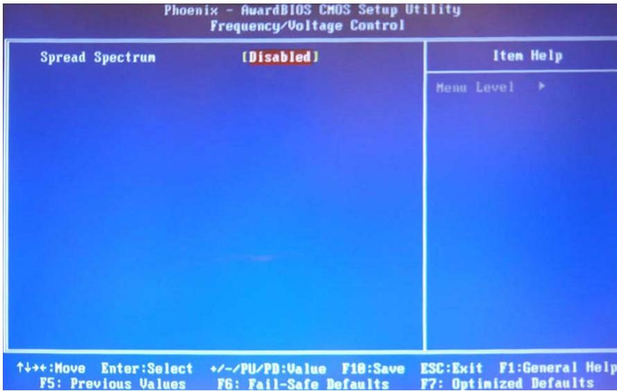
![Phoenix - AwardBIOS CMOS Setup Utility\nFrequency/Voltage Control\nSpread Spectrum (Disabled) Item Help\nMenu Level )\n↑↓++:Move Enter:Select +/-/PU/PD:Value F10:Save ESC:Exit F1:General Help\nF5: Previous Values F6: Fail-Safe Defaults F7: Optimized Defaults](.m-302-50-13062-1010-201-en/c0582d5e2f75f53bcb12630c485c53238f7cac1b75d07bf1117ab2b160ea4dd8.jpg)

# Spread Spectrum

This setting allows you to reduce EMI by modulating the signals the CPU generates so that the spikes are reduced to flatter curves. This is achieved by varying the frequency slightly so that the signal does not use any particular frequency for more than a moment. The options are “Disabled” and “Enabled”.

# 4.9 Load Fail-Safe Defaults

Use this menu to load the BIOS default values for the minimal/stable performance for your system to operate. Press &lt;Y&gt; to load the BIOS default values for the most stable, minimal-performance system operations.
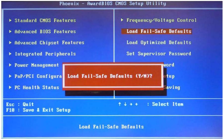
![Phoenix - AwardBIOS CMOS Setup Utility\n► Standard CMOS Features\n► Advanced BIOS Features\n► Advanced Chipset Features\n► Integrated Peripherals\n► Power Management\n► PnP/PCI Configura\n► PC Health Status\n► Frequency/Voltage Control\nLoad Fail-Safe Defaults\nLoad Optimized Defaults\nSet Supervisor Password\nLoad Fail-Safe Defaults (Y/N)?\n► Saving\nEsc : Quit\nF10 : Save & Exit Setup\n↑↓→← : Select Item\nLoad Fail-Safe Defaults](.m-302-50-13062-1010-201-en/ad5391467ef3662b2cc7dfbd57ca7b1c1d7c643649e99cbd6f9a0b1feec14ddd.jpg)

# 4.10 Load Optimized Defaults

Use this menu to load the BIOS default values that are factory settings for optimal performance system operations. While Award has designed the custom BIOS to maximize performance, the factory can change these defaults to meet its needs. Press &lt;Y&gt; to load the default values setting for optimal performance system operations.
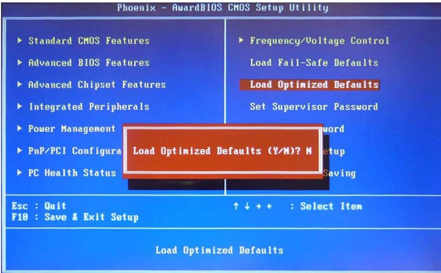
![Phoenix - AwardBIOS CMOS Setup Utility\n► Standard CMOS Features\n► Advanced BIOS Features\n► Advanced Chipset Features\n► Integrated Peripherals\n► Power Management\n► PnP/PCI Configura\n► PC Health Status\n► Frequency/Voltage Control\nLoad Fail-Safe Defaults\nLoad Optimized Defaults\nSet Supervisor Password\nLoad Optimized Defaults (Y/N)? N\nSetup\nSaving\nEsc : Quit\nF10 : Save & Exit Setup\n↑↓→← : Select Item\nLoad Optimized Defaults](.m-302-50-13062-1010-201-en/cfb08c49b2f147f6ac9df8a361d9f9bbcfb0ab9d2c27a1cea10dcd5f4557a676.jpg)

# 4.11 Set Supervisor & User Password

These two options set the system password. Supervisor Password sets a password that will be used to protect the system and Setup utility. User Password sets a password that will be used exclusively on the system. To specify a password, highlight the type you want and press &lt; Enter &gt;. The “Enter Password:” message prompts you on the screen. Type the password, up to eight characters in length, and press &lt; Enter &gt;. The system confirms your password by asking you to type it again. After setting a password, the screen automatically returns to the main screen.
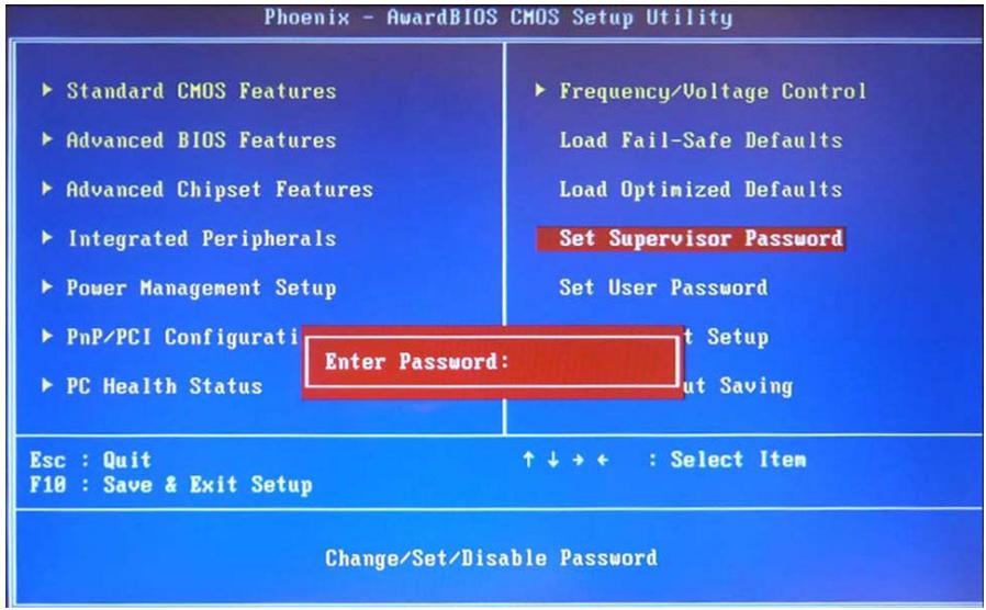
![Phoenix - AwardBIOS CMOS Setup Utility\n► Standard CMOS Features\n► Advanced BIOS Features\n► Advanced Chipset Features\n► Integrated Peripherals\n► Power Management Setup\n► PnP/PCI Configurati\n► PC Health Status\n► Frequency/Voltage Control\nLoad Fail-Safe Defaults\nLoad Optimized Defaults\nSet Supervisor Password\nSet User Password\nEnter Password:\nPnP/PCI Setup\nPC Health Status\nEsc : Quit\nF10 : Save & Exit Setup\n↑↓→← : Select Item\nChange/Set/Disable Password](.m-302-50-13062-1010-201-en/1ab262852057e120c8eb46f665b6c55fcc27362df3550880644f86826ebdf994.jpg)

# 4.12 Save & Exit Setup

This option allows you to determine whether to accept any modifications or not. Typing Y will quit the setup utility and save all changes into the CMOS memory. Typing N will return to the Setup Utility Main Screen.
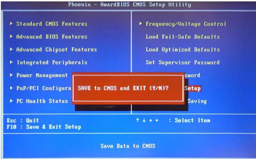
![Phoenix - AwardBIOS CMOS Setup Utility\n► Standard CMOS Features\n► Advanced BIOS Features\n► Advanced Chipset Features\n► Integrated Peripherals\n► Power Management\n► PnP/PCI Configura SAVE to CMOS and EXIT (Y/N)?\n► PC Health Status Setup\n► Frequency/Voltage Control\nLoad Fail-Safe Defaults\nLoad Optimized Defaults\nSet Supervisor Password\n► Sword\n► Setup\n► Saving\nEsc : Quit ↑↓→← : Select Item\nF10 : Save & Exit Setup\nSave Data to CMOS](.m-302-50-13062-1010-201-en/5587344b3232c375bfd7178ae7645cab054def4e3178a5427d6de1cd8e8dc22b.jpg)

# 4.13 Exit Without Saving

Select this option to exit the Setup utility without saving the changes you have made in this session. Typing Y will quit the Setup utility without saving any modifications. Typing N will return to Setup utility.
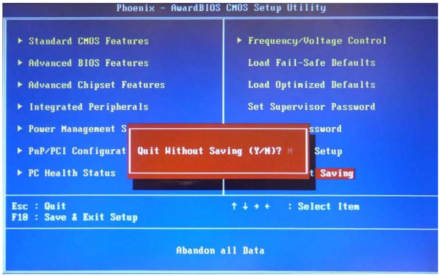
![Phoenix - AwardBIOS CMOS Setup Utility\n► Standard CMOS Features\n► Advanced BIOS Features\n► Advanced Chipset Features\n► Integrated Peripherals\n► Power Management S\n► PnP/PCI Configurat\n► PC Health Status\n► Frequency/Voltage Control\nLoad Fail-Safe Defaults\nLoad Optimized Defaults\nSet Supervisor Password\nQuit Without Saving (Y/N)? N\nSetup\nQuit Saving\nEsc : Quit\nF10 : Save & Exit Setup\n↑↓→← : Select Item\nAbandon all Data](.m-302-50-13062-1010-201-en/b668e838bbd6c1a63688b96b8b1cdd24d1efd7b0dbd9597013400df3f7699e6d.jpg)

This page intentionally left blank.

# 5 POST Codes

The following is a list of M-302 POST Codes.

<table><tr><td>Code (hex)</td><td>Description</td></tr><tr><td>CFh</td><td>Test CMOS read/write functionality</td></tr><tr><td>C0h</td><td>Early chipset initialization: Disable shadow RAM, L2 cache (socket 7 and below), program basic chipset registers</td></tr><tr><td>C1h</td><td>Detect memory: Auto detection of DRAM size, type and ECC, auto detection of L2 cache (socket 7 and below)</td></tr><tr><td>C3h</td><td>Expand compressed BIOS code to DRAM</td></tr><tr><td>C5h</td><td>Call chipset hook to copy BIOS back to E000 &amp; F000 shadow RAM</td></tr><tr><td>01h</td><td>Expand the Xgroup codes located in physical memory address 1000:0</td></tr><tr><td>02h</td><td>Reserved</td></tr><tr><td>03h</td><td>Initial SuperIO_Early_Init switch</td></tr><tr><td>04h</td><td>Reserved</td></tr><tr><td>05h</td><td>Blank out screen; Clear CMOS error flag</td></tr><tr><td>06h</td><td>Reserved</td></tr><tr><td>07h</td><td>Clear 8042 interface; Initialize 8042 self test</td></tr><tr><td>08h</td><td>Test special keyboard controller for Winbond 977 series Super I/O chips; Enable keyboard interface</td></tr><tr><td>09h</td><td>Reserved</td></tr><tr><td>0Ah</td><td>Disable PS/2 mouse interface (optional); Auto detect ports for keyboard &amp; mouse followed by a port &amp; interface swap (optional); Reset keyboard for Winbond 977 series Super I/O chips</td></tr><tr><td>0Bh</td><td>Reserved</td></tr><tr><td>0Ch</td><td>Reserved</td></tr><tr><td>0Dh</td><td>Reserved</td></tr><tr><td>0Eh</td><td>Test F000h segment shadow to see whether it is read/write capable or not. If test fails, keep beeping the speaker</td></tr><tr><td>0Fh</td><td>Reserved</td></tr><tr><td>10h</td><td>Auto detect flash type to load appropriate flash read/write codes into the run time area in F000 for ESCD &amp; DMI support</td></tr><tr><td>11h</td><td>Reserved</td></tr><tr><td>12h</td><td>Use walking 1's algorithm to check out interface in CMOS circuitry. Also set real time clock power status and then check for override</td></tr><tr><td>13h</td><td>Reserved</td></tr><tr><td>14h</td><td>Program chipset default values into chipset. Chipset default values are MODBINable by OEM customers</td></tr><tr><td>15h</td><td>Reserved</td></tr><tr><td>16h</td><td>Initial Early_Init_Onboard_Generator switch</td></tr><tr><td>17h</td><td>Reserved</td></tr><tr><td>18h</td><td>Detect CPU information including brand, SMI type (Cyrix or Intel) and CPU level (586 or 686)</td></tr><tr><td>19h</td><td>Reserved</td></tr><tr><td>1Ah</td><td>Reserved</td></tr><tr><td>1Bh</td><td>Initial interrupts vector table. If no special specified, all H/W interrupts are directed to SPURIOUS_INT_HDLR &amp; S/W interrupts to SPURIOUS_soft_HDLR</td></tr><tr><td>1Ch</td><td>Reserved</td></tr><tr><td>1Dh</td><td>Initial EARLY_PM_INIT switch</td></tr><tr><td>1Eh</td><td>Reserved</td></tr><tr><td>1Fh</td><td>Load keyboard matrix (notebook platform)</td></tr><tr><td>20h</td><td>Reserved</td></tr><tr><td>21h</td><td>HPM initialization (notebook platform)</td></tr><tr><td>22h</td><td>Reserved</td></tr><tr><td>23h</td><td>Check validity of RTC value; Load CMOS settings into BIOS stack. If CMOS checksum fails, use default value instead; Prepare BIOS resource map for PCI &amp; PnP use. If ESCD is valid, take into consideration of the ESCD's legacy information; Onboard clock generator initialization. Disable respective clock resource to empty PCI &amp; DIMM slots; Early PCI initialization - Enumerate PCI bus number, assign memory &amp; I/O resource, search for a valid VGA device &amp; VGA BIOS, and put it into C000:0</td></tr><tr><td>24h</td><td>Reserved</td></tr><tr><td>25h</td><td>Reserved</td></tr><tr><td>26h</td><td>Reserved</td></tr><tr><td>27h</td><td>Initialize INT 09 buffer</td></tr><tr><td>28h</td><td>Reserved</td></tr><tr><td>29h</td><td>Program CPU internal MTRR (P6 &amp; PII) for 0-640K memory address; Initialize the APIC for Pentium class CPU; Program early chipset according to CMOS setup; Measure CPU speed; Invoke video BIOS</td></tr><tr><td>2Ah</td><td>Reserved</td></tr><tr><td>2Bh</td><td>Reserved</td></tr><tr><td>2Ch</td><td>Reserved</td></tr><tr><td>2Dh</td><td>Initialize multilanguage; Put information on screen display, including Award title, CPU type, CPU speed, etc...</td></tr><tr><td>2Eh</td><td>Reserved</td></tr><tr><td>2Fh</td><td>Reserved</td></tr><tr><td>30h</td><td>Reserved</td></tr><tr><td>31h</td><td>Reserved</td></tr><tr><td>32h</td><td>Reserved</td></tr><tr><td>33h</td><td>Reset keyboard except Winbond 977 series Super I/O chips</td></tr><tr><td>34h</td><td>Reserved</td></tr><tr><td>35h</td><td>Reserved</td></tr><tr><td>36h</td><td>Reserved</td></tr><tr><td>37h</td><td>Reserved</td></tr><tr><td>38h</td><td>Reserved</td></tr><tr><td>39h</td><td>Reserved</td></tr><tr><td>3Ah</td><td>Reserved</td></tr><tr><td>3Bh</td><td>Reserved</td></tr><tr><td>3Ch</td><td>Test 8254</td></tr><tr><td>3Dh</td><td>Reserved</td></tr><tr><td>3Eh</td><td>Test 8259 interrupt mask bits for channel 1</td></tr><tr><td>3Fh</td><td>Reserved</td></tr><tr><td>40h</td><td>Test 9259 interrupt mask bits for channel 2</td></tr><tr><td>41h</td><td>Reserved</td></tr><tr><td>42h</td><td>Reserved</td></tr><tr><td>43h</td><td>Test 8259 functionality</td></tr><tr><td>44h</td><td>Reserved</td></tr><tr><td>45h</td><td>Reserved</td></tr><tr><td>46h</td><td>Reserved</td></tr><tr><td>47h</td><td>Initialize EISA slot</td></tr><tr><td>48h</td><td>Reserved</td></tr><tr><td>49h</td><td>Calculate total memory by testing the last double last word of each 64K page; Program writes allocation for AMD K5 CPU</td></tr><tr><td>4Ah</td><td>Reserved</td></tr><tr><td>4Bh</td><td>Reserved</td></tr><tr><td>4Ch</td><td>Reserved</td></tr><tr><td>4Dh</td><td>Reserved</td></tr><tr><td>4Eh</td><td>Program MTRR of M1 CPU; initialize L2 cache for P6 class CPU &amp; program cacheable range; Initialize the APIC for P6 class CPU; On MP platform, adjust the cacheable range to smaller one in case the cacheable ranges between each CPU are not identical</td></tr><tr><td>4Fh</td><td>reserved</td></tr><tr><td>50h</td><td>Initialize USB</td></tr><tr><td>51h</td><td>Reserved</td></tr><tr><td>52h</td><td>Test all memory (clear all extended memory to 0)</td></tr><tr><td>53h</td><td>Reserved</td></tr><tr><td>54h</td><td>Reserved</td></tr><tr><td>55h</td><td>Display number of processors (multi-processor platform)</td></tr><tr><td>56h</td><td>Reserved</td></tr><tr><td>57h</td><td>Display PnP logo; Early ISA PnP initialization and assign CSN to every ISA PnP device</td></tr><tr><td>58h</td><td>Reserved</td></tr><tr><td>59h</td><td>Initialize the combined Trend Anti-Virus code</td></tr><tr><td>5Ah</td><td>Reserved</td></tr><tr><td>5Bh</td><td>Show message for entering AWDFLASH.EXE from FDD (optional feature)</td></tr><tr><td>5Ch</td><td>Reserved</td></tr><tr><td>5Dh</td><td>Initialize Init_Onboard_Super_IO switch; Initialize Init_Onboard_AUDIO switch</td></tr><tr><td>5Eh</td><td>Reserved</td></tr><tr><td>5Fh</td><td>Reserved</td></tr><tr><td>60h</td><td>Okay to enter Setup utility</td></tr><tr><td>61h</td><td>Reserved</td></tr><tr><td>62h</td><td>Reserved</td></tr><tr><td>63h</td><td>Reserved</td></tr><tr><td>64h</td><td>Reserved</td></tr><tr><td>65h</td><td>Initialize PS/2 mouse</td></tr><tr><td>66h</td><td>Reserved</td></tr><tr><td>67h</td><td>Prepare memory size information for function call: INT 15h ax=E820h</td></tr><tr><td>68h</td><td>Reserved</td></tr><tr><td>69h</td><td>Turn on L2 cache</td></tr><tr><td>6Ah</td><td>Reserved</td></tr><tr><td>6Bh</td><td>Program chipset registers according to items described in Setup &amp; Auto-Configuration table</td></tr><tr><td>6Ch</td><td>Reserved</td></tr><tr><td>6Dh</td><td>Assign resources to all ISA PnP devices; Auto assign ports to onboard COM ports if the corresponding item in Setup is set to "AUTO"</td></tr><tr><td>6Eh</td><td>Reserved</td></tr><tr><td>6Fh</td><td>Initialize floppy controller; Setup floppy related fields in 40:hardware</td></tr><tr><td>70h</td><td>Reserved</td></tr><tr><td>71h</td><td>Reserved</td></tr><tr><td>72h</td><td>Reserved</td></tr><tr><td>73h</td><td>Enter AWDFLASH.EXE if: AWDFLASH.EXE is found in floppy dive and ALT+F2 is pressed</td></tr><tr><td>74h</td><td>Reserved</td></tr><tr><td>75h</td><td>Detect and install all IDE devices: HDD, LS120, ZIP, CDROM...</td></tr><tr><td>76h</td><td>Reserved</td></tr><tr><td>77h</td><td>Detect serial ports and parallel ports</td></tr><tr><td>78h</td><td>Reserved</td></tr><tr><td>79h</td><td>Reserved</td></tr><tr><td>7Ah</td><td>Detect and install coprocessor</td></tr><tr><td>7Bh</td><td>Reserved</td></tr><tr><td>7Ch</td><td>Reserved</td></tr><tr><td>7Dh</td><td>Reserved</td></tr><tr><td>7Eh</td><td>Reserved</td></tr><tr><td>7Fh</td><td>Switch back to text mode if full screen logo is supported: if errors occur, report errors &amp; wait for keys, if no errors occur or F1 key is pressed continue - Clear EPA or customization logo</td></tr><tr><td>80h</td><td>Reserved</td></tr><tr><td>81h</td><td>Reserved</td></tr><tr><td>82H</td><td>Call chipset power management hook: Recover the text fond used by EPA logo (not for full screen logo), If password is set, ask for password</td></tr><tr><td>83H</td><td>Save all data in stack back to CMOS</td></tr><tr><td>84h</td><td>Initialize ISA PnP boot devices</td></tr><tr><td>85h</td><td>Final USB initialization; NET PC: Build SYSID structure; Switch screen back to text mode; Set up ACPI table at top of memory; Invoke ISA adapter ROM's; Assign IRQ's to PCI devices; Initialize APM; Clear noise of IRQ's</td></tr><tr><td>86h</td><td>Reserved</td></tr><tr><td>87h</td><td>Reserved</td></tr><tr><td>88h</td><td>Reserved</td></tr><tr><td>89h</td><td>Reserved</td></tr><tr><td>90h</td><td>Reserved</td></tr><tr><td>91h</td><td>Reserved</td></tr><tr><td>92h</td><td>Reserved</td></tr><tr><td>93h</td><td>Read HDD boot sector information for Trend Anti-Virus code</td></tr><tr><td>94h</td><td>Enable L2 cache; Program boot up speed; Chipset final initialization; Power management final initialization; Clear screen and display summary table; Program K^ write allocation; Program P6 class write combining</td></tr><tr><td>95h</td><td>Program daylight saving; Update keyboard LED and typematic rate</td></tr><tr><td>96h</td><td>Build MP table; Build and update ESCD; Set CMOS century to 20h or 19h; Load CMOS time into DOS timer tick; Build MSIRQ routing table</td></tr><tr><td>FFh</td><td>Boot attempt (INT 19h)</td></tr></table>

# Appendix A - Watchdog Timer

The following is a sample program for configuring the M-302's watchdog timer.

# A.1 Sample Code

# Unlock W83627DHG-A:

```txt
outportb(0x2E, 0x87) ;Unlock Super I/O
```

# Select Logical Device:

```txt
outportb(0x2E, 0x07) ;Select device number register
outportb(0x2F, 0x08);Set to Logical Device 8
```

# Activate WDT:

```txt
outportb(0x2E, 0x30) ;Select WDTO# activate register
outportb(0x2F, 0x01) ;Enable watchdog
```

# Set Seconds or Minutes:

```txt
outportb(0x2E, 0xF5) ;Select WDTO# control register
outportb(0x2F, mode) ;where mode=0x00(Sec) or 0x08(Min)
```

# Set Base Timer:

```txt
outportb(0x2E, 0xF6) ;Select WDTO# counter register
outportb(0x2F, timeout);where timeout=0x00~0xFF
```

# Reset Timeout Counter:

```txt
outportb(0x2E, 0xF6) ;Select WDTO# counter register
outportb(0x2F, timeout);where timeout=0x00~0xFF
```

This page intentionally left blank.

# Appendix B - System Resources

B.1 System Memory Map

<table><tr><td>Address Range (decimal)</td><td>Address Range (hex)</td><td>Size</td><td>Description</td></tr><tr><td>(4GB-2MB)</td><td>FFE00000 – FFFFFFFF</td><td>2 MB</td><td>High BIOS Area</td></tr><tr><td>(4GB-18MB) – (4GB-17MB-1)</td><td>FEE00000 – FEEFFFFF</td><td>1 MB</td><td>FSB Interrupt Memory Space</td></tr><tr><td>(4GB-20MB) – (4GB-19MB-1)</td><td>FEC00000 – FECFFFFFF</td><td>1 MB</td><td>APIC Configuration Space</td></tr><tr><td>15MB – 16MB</td><td>F00000 – FFFFFFF</td><td>1 MB</td><td>ISA Hole</td></tr><tr><td>960 K – 1024 K</td><td>F0000 – FFFFF</td><td>64 KB</td><td>System BIOS Area</td></tr><tr><td>896 K – 960 K</td><td>E0000 – EFFFF</td><td>64 KB</td><td>Extended System BIOS Area</td></tr><tr><td>768 K – 896 K</td><td>C0000 – DFFFF</td><td>128 KB</td><td>PCI expansion ROM areaC0000 – CBFFF: Onboard VGA BIOS CC000 – CCFFF: Intel 82566DM PXE option ROM when onboard LAN boot ROM is enabled.</td></tr><tr><td>640 K – 768 K</td><td>A0000 – BFFFF</td><td>128 KB</td><td>Video Buffer &amp; SMM space</td></tr><tr><td>0 K – 640 K</td><td>00000 – 9FFFF</td><td>640 KB</td><td>DOS Area</td></tr></table>

Table B-1: System Memory Map
Note: Whole D0000H segment except PXE occupied area can be forwarded to ISA bus.

# B.2 Direct Memory Access Channels

<table><tr><td>Channel Number</td><td>Data Width</td><td>System Resource</td></tr><tr><td>0</td><td>8-bits</td><td>Parallel port(1)</td></tr><tr><td>1</td><td>8-bits</td><td>Parallel port(1)</td></tr><tr><td>2</td><td>8-bits</td><td>Diskette drive(1)</td></tr><tr><td>3</td><td>8-bits</td><td>Parallel port(1)</td></tr><tr><td>4</td><td></td><td>Reserved - cascade channel</td></tr><tr><td>5</td><td>16-bits</td><td>Open</td></tr><tr><td>6</td><td>16-bits</td><td>Open</td></tr><tr><td>7</td><td>16-bits</td><td>Open</td></tr></table>

# Table B-2: Direct Memory Access Channels

Note(1): DMA channel 1/3 is selected when using parallel port. Floppy (Winbond default uses DMA 02) and parallel port cannot be used at the same time.

B.3 Fixed I/O Map

<table><tr><td>Hex Range</td><td>Device</td></tr><tr><td>000-01F</td><td>DMA controller 1, 82C37 equivalent</td></tr><tr><td>020-02D and 030-03F</td><td>Interrupt controller 1, 8259 equivalent</td></tr><tr><td>02E-02F</td><td>LPC SIO (W83627) configuration index/data registers</td></tr><tr><td>040-042-043</td><td>Timer/Counter</td></tr><tr><td>4E-4F</td><td>N/A</td></tr><tr><td>061</td><td>NMI controller</td></tr><tr><td>60,62,64,66</td><td>N/A(MicroController)</td></tr><tr><td>070-077</td><td>Real Time Clock Controller</td></tr><tr><td>080-9F</td><td>DMA Controller, or LPC or PCI</td></tr><tr><td>0A0-0AD and 0B4-0BD</td><td>Interrupt controller</td></tr><tr><td>0B2 and 0B3</td><td>Power Management</td></tr><tr><td>0C0-0DF</td><td>DMA controller</td></tr><tr><td>0F0</td><td>Read PCI and Master Abord, Write FERR#/IGNNE#/Interrupt Controller</td></tr><tr><td>0170-177</td><td>SATA Controller, or PCI</td></tr><tr><td>01F0-1F7</td><td>SATA Controller, or PCI</td></tr><tr><td>0376</td><td>SATA Controller, or PCI</td></tr><tr><td>03F6</td><td>SATA Controller, or PCI</td></tr><tr><td>04D0-4D1</td><td>Interrupt Controller</td></tr><tr><td>0CF9</td><td>Reset Generator</td></tr></table>

Table B-3: Fixed I/O Map

B.4 Variable I/O Map

<table><tr><td>Hex Range</td><td>Device</td></tr><tr><td>400</td><td>ACPI</td></tr><tr><td>Anywhere in 64KB I/O Space</td><td>USB UHCI Controller #1</td></tr><tr><td>Anywhere in 64KB I/O Space</td><td>USB UHCI Controller #2</td></tr><tr><td>Anywhere in 64KB I/O Space</td><td>USB UHCI Controller #3</td></tr><tr><td>Anywhere in 64KB I/O Space</td><td>USB UHCI Controller #4</td></tr><tr><td>Anywhere in 64KB I/O Space</td><td>USB UHCI Controller #5</td></tr><tr><td>500</td><td>SMBUS</td></tr><tr><td>460</td><td>TCO</td></tr><tr><td>480</td><td>GPIO</td></tr><tr><td>378-37F</td><td>Parallel Port</td></tr><tr><td>3F8/2F8/3E8/2E8</td><td>Serial Port 1 Serial Port 2</td></tr><tr><td>3E8/2E8</td><td>Serial Port 3, Serial Port 4</td></tr><tr><td>3F0-3F7</td><td>Floppy Controller</td></tr><tr><td>290</td><td>Hardware Monitor</td></tr></table>

Table B-4: Variable I/O Map

# B.5 Interrupt Request (IRQ) Lines

IRQ Lines PIC Mode

<table><tr><td>IRQ#</td><td>Typical Interrupt Resource</td><td>Connected to Pin</td><td>Available</td></tr><tr><td>0</td><td>Counter 0</td><td>N/A</td><td>No</td></tr><tr><td>1</td><td>Keyboard controller</td><td>N/A</td><td>No</td></tr><tr><td>2</td><td>Cascade interrupt from slave PIC</td><td>N/A</td><td>No</td></tr><tr><td>3</td><td>Serial Port 2 (COM2) / PCI / ISA</td><td>IRQ3 via SERIRQ, IRQ3 at ISA bus</td><td>Note (1)</td></tr><tr><td>4</td><td>Serial Port 1 (COM1) / PCI / ISA</td><td>IRQ4 via SERIRQ, IRQ4 at ISA bus</td><td>Note (1)</td></tr><tr><td>5</td><td>Serial Port 3, (COM3) / PCI / ISA</td><td>IRQ5 via SERIRQ, IRQ5 at ISA bus</td><td>Note (1)</td></tr><tr><td>6</td><td>Floppy Drive Controller</td><td>IRQ6 via SERIRQ</td><td>No</td></tr><tr><td>7</td><td>Parallel Port 1 (LPT1) / PCI / ISA</td><td>IRQ7 via SERIRQ, IRQ7 at ISA bus</td><td>Note (1)</td></tr><tr><td>8</td><td>Real-time clock</td><td>N/A</td><td>No</td></tr><tr><td>9</td><td>SCI / PCI</td><td>IRQ9 via SERIRQ, IRQ9 at ISA bus</td><td>Note (1), (2)</td></tr><tr><td>10</td><td>Serial Port 4, PCI / ISA</td><td>IRQ10 via SERIRQ, IRQ10 at ISA bus</td><td>Note (1)</td></tr><tr><td>11</td><td>PCI / ISA</td><td>IRQ11 via SERIRQ, IRQ11 at ISA bus</td><td>Note (1)</td></tr><tr><td>12</td><td>PS/2 Mouse / PCI / ISA</td><td>IRQ12 via SERIRQ, IRQ12 at ISA bus</td><td>Note (1)</td></tr><tr><td>13</td><td>Math Processor</td><td>N/A</td><td>No</td></tr><tr><td>14</td><td>Primary IDE controller / PCI / ISA</td><td>IRQ14 via SERIRQ, IRQ14 at ISA bus</td><td>Note (1)</td></tr><tr><td>15</td><td>Secondary IDE controller / PCI / ISA</td><td>IRQ15 via SERIRQ, IRQ15 at ISA bus</td><td>Note (1)</td></tr></table>

Table B-5: IRQ Lines PIC Mode

Note(1): These IRQs can be used for PCI devices when onboard device is disabled. If IRQ is from ISA, user must reserve IRQ for ISA in BIOS setup menu.

Note (2): BIOS does not open IRQ 9 setting for ISA bus.

IRQ Lines APIC Mode

<table><tr><td>IRQ#</td><td>Typical Interrupt Resource</td><td>Connected to Pin</td><td>Available</td></tr><tr><td>0</td><td>System Timer</td><td>N/A</td><td>No</td></tr><tr><td>1</td><td>Keyboard controller</td><td>N/A</td><td>No</td></tr><tr><td>2</td><td>Cascade interrupt from slave PIC</td><td>N/A</td><td>No</td></tr><tr><td>3</td><td>Serial Port 2 (COM2) / PCI / ISA</td><td>IRQ3 via SERIRQ, IRQ3 at ISA bus</td><td>Note (1)</td></tr><tr><td>4</td><td>Serial Port 1 (COM1) / PCI / ISA</td><td>IRQ4 via SERIRQ, IRQ4 at ISA bus</td><td>Note (1)</td></tr><tr><td>5</td><td>Serial Port 3 (COM3) / PCI / ISA</td><td>IRQ5 via SERIRQ, IRQ5 at ISA bus</td><td>Note (1)</td></tr><tr><td>6</td><td>Floppy Drive Controller</td><td>IRQ6 via SERIRQ</td><td>No</td></tr><tr><td>7</td><td>Parallel Port 1 (LPT1) / PCI / ISA</td><td>IRQ7 via SERIRQ, IRQ7 at ISA bus</td><td>Note (1)</td></tr><tr><td>8</td><td>Real-time clock</td><td>N/A</td><td>No</td></tr><tr><td>9</td><td>SCI / PCI</td><td>IRQ9 via SERIRQ, IRQ9 at ISA bus</td><td>Note (1), (2)</td></tr><tr><td>10</td><td>Serial Port 4/PCI / ISA</td><td>IRQ10 via SERIRQ, IRQ10 at ISA bus</td><td>Note (1)</td></tr><tr><td>11</td><td>PCI / ISA</td><td>IRQ11 via SERIRQ, IRQ11 at ISA bus</td><td>Note (1)</td></tr><tr><td>12</td><td>PS/2 Mouse / PCI / ISA</td><td>IRQ12 via SERIRQ, IRQ12 at ISA bus</td><td>Note (1)</td></tr><tr><td>13</td><td>Math Processor</td><td>N/A</td><td>No</td></tr><tr><td>14</td><td>Primary IDE controller / PCI / ISA</td><td>IRQ14 via SERIRQ, IRQ14 at ISA bus</td><td>Note (1)</td></tr><tr><td>15</td><td>Secondary IDE controller / PCI / ISA</td><td>IRQ15 via SERIRQ, IRQ15 at ISA bus</td><td>Note (1)</td></tr><tr><td>16</td><td>N/A</td><td>PCI Slot INT A, Q965 express chipset, ICH8 root port 1,ICH8 root port 5, USB Universal, PCI express root port 2991,PCI IDE controller</td><td>Yes</td></tr></table>

<table><tr><td>IRQ#</td><td>Typical Interrupt Resource</td><td>Connected to Pin</td><td>Available</td></tr><tr><td>17</td><td>N/A</td><td>PCI Slot INT B</td><td>Yes</td></tr><tr><td>18</td><td>N/A</td><td>PCI Slot INT C, UHCI Controller 2, EHCI Controller 1, SMBUS, SATA controller 0</td><td>Yes</td></tr><tr><td>19</td><td>N/A</td><td>PCI Slot INT D, UHCI Controller 1, SATA controller1</td><td>Yes</td></tr><tr><td>20</td><td>N/A</td><td>ICH8 internal GBE controller, TI OHCI 1394 Controller</td><td>No</td></tr><tr><td>21</td><td>N/A</td><td>UHCI Controller 5</td><td>No</td></tr><tr><td>22</td><td>N/A</td><td>ICH8 HDA</td><td>No</td></tr><tr><td>23</td><td>N/A</td><td>UHCI Controller 0, EHCI Controller 0</td><td>No</td></tr></table>

Table B-6: IRQ Lines APIC Mode

Note (1): These IRQs can be used for PCI devices when onboard device is disabled. If IRQ is from ISA, user must reserve IRQ for ISA in BIOS setup menu.

Note (2): BIOS does not open IRQ 9 setting for ISA bus.

B.6 PCI Configuration Space Map

<table><tr><td>Bus #</td><td>Device #</td><td>Function #</td><td>Routing</td><td>Description</td></tr><tr><td>00h</td><td>00h</td><td>00h</td><td>N/A</td><td>Intel 965 GME GMCH Host-Hub Interface Bridge</td></tr><tr><td>00h</td><td>01h</td><td>00h</td><td>Internal</td><td>P.E.G. Root Port</td></tr><tr><td>00h</td><td>02h</td><td>00h</td><td>Internal</td><td>Intel Integrated Graphics Device</td></tr><tr><td>00h</td><td>02h</td><td>00h</td><td>Internal</td><td>Intel Integrated Graphics Device</td></tr><tr><td>02h</td><td>00H</td><td>0FFh</td><td>N/A</td><td>P.E.G. Port</td></tr><tr><td>00h</td><td>19h</td><td>00h</td><td>Internal</td><td>GbE Controller</td></tr><tr><td>00h</td><td>1Ah</td><td>00h</td><td>Internal</td><td>Intel USB UHCI Controller 4</td></tr><tr><td>00h</td><td>1Ah</td><td>01h</td><td>Internal</td><td>Intel USB UHCI Controller 5</td></tr><tr><td>00h</td><td>1Ah</td><td>07h</td><td>Internal</td><td>Intel USB EHCI Controller 1</td></tr><tr><td>00h</td><td>1Bh</td><td>00h</td><td>Internal</td><td>High Definition Audio controller</td></tr><tr><td>00h</td><td>1Ch</td><td>00h</td><td>Internal</td><td>Intel ICH Express Root port 0</td></tr><tr><td>00h</td><td>1Ch</td><td>01h</td><td>Internal</td><td>Intel ICH Express Root port 1</td></tr><tr><td>00h</td><td>1Ch</td><td>02h</td><td>Internal</td><td>Intel ICH Express Root port 2</td></tr><tr><td>00h</td><td>1Ch</td><td>03h</td><td>Internal</td><td>Intel ICH Express Root port 3</td></tr><tr><td>00h</td><td>1Ch</td><td>04h</td><td>Internal</td><td>Intel ICH Express Root port 4</td></tr><tr><td>00h</td><td>1Ch</td><td>05h</td><td>Internal</td><td>Intel ICH Express Root port 5</td></tr><tr><td>00h</td><td>1Dh</td><td>00h</td><td>Internal</td><td>Intel USB UHCI Controller 0</td></tr><tr><td>00h</td><td>1Dh</td><td>01h</td><td>Internal</td><td>Intel USB UHCI Controller 1</td></tr><tr><td>00h</td><td>1Dh</td><td>02h</td><td>Internal</td><td>Intel USB UHCI Controller 2</td></tr><tr><td>00h</td><td>1Dh</td><td>03h</td><td>Internal</td><td>Intel USB UHCI Controller 3</td></tr><tr><td>00h</td><td>1Dh</td><td>07h</td><td>Internal</td><td>Intel USB EHCI Controller</td></tr><tr><td>00h</td><td>1Eh</td><td>00h</td><td>N/A</td><td>Intel Hub Interface to PCI Bridge</td></tr><tr><td>00h</td><td>1Fh</td><td>00h</td><td>N/A</td><td>Intel LPC Interface Bridge</td></tr><tr><td>00h</td><td>1Fh</td><td>01h</td><td>Internal</td><td>Intel IDE Controller</td></tr><tr><td>00h</td><td>1Fh</td><td>02h</td><td>Internal</td><td>Intel SATA controller</td></tr><tr><td>00h</td><td>1Fh</td><td>03h</td><td>Internal</td><td>Intel SMBus Controller</td></tr><tr><td>00h</td><td>1Fh</td><td>05h</td><td>Internal</td><td>Intel SATA controller1</td></tr><tr><td>00h</td><td>1Fh</td><td>06h</td><td>Internal</td><td>Thermal Controller</td></tr><tr><td>01h</td><td>00h</td><td>0FFh</td><td>Internal</td><td>NB PCIE Port #0</td></tr><tr><td>02h</td><td>00h</td><td>0FFh</td><td>Internal</td><td>SB PCIE Port X4 #0</td></tr></table>

<table><tr><td>Bus #</td><td>Device #</td><td>Function #</td><td>Routing</td><td>Description</td></tr><tr><td>03h</td><td>00h</td><td>000h</td><td>Internal(PI RQA,B,C, D)</td><td>JMicron ATA 2363 (SB PCIE Port #1)</td></tr><tr><td>04h</td><td>03h</td><td>0FFh</td><td>PIRQA,B, C,D</td><td>External PCI Slot 1</td></tr><tr><td>04h</td><td>01h</td><td>000h</td><td>PIRQE(IN TA) only</td><td>TI 1394 2 (SB PCI bridge)</td></tr><tr><td>04h</td><td>04h</td><td>0FFh</td><td>PIRQB,C, D,A</td><td>External PCI Slot 2</td></tr><tr><td>04h</td><td>05h</td><td>0FFh</td><td>PIRQC,D, A,B</td><td>External PCI Slot 3</td></tr><tr><td>04h</td><td>06h</td><td>0FFh</td><td>PIRQD,A, B,C</td><td>External PCI Slot 4</td></tr><tr><td>04h</td><td>07h</td><td>0FFh</td><td>PIRQF,G,H ,E</td><td>External PCI Slot 5</td></tr></table>

Table B-7: PCI Configuration Space Map

B.7 PCI Interrupt Routing Map

<table><tr><td>INT Line</td><td>INT0</td><td>INT1</td><td>INT2</td><td>INT3</td></tr><tr><td>P.E.G. Root Port</td><td>X</td><td>X</td><td>X</td><td>X</td></tr><tr><td>VGA</td><td>X</td><td></td><td></td><td></td></tr><tr><td>IDE Controllerr</td><td>X</td><td></td><td></td><td></td></tr><tr><td>SATAController1</td><td></td><td>X</td><td></td><td></td></tr><tr><td>SMBUS</td><td></td><td></td><td>X</td><td></td></tr><tr><td>Thermal Controller</td><td></td><td></td><td>X</td><td></td></tr><tr><td>UHCI 0</td><td>X</td><td></td><td></td><td></td></tr><tr><td>UHCI 1</td><td></td><td>X</td><td></td><td></td></tr><tr><td>UHCI 2</td><td></td><td></td><td>X</td><td></td></tr><tr><td>UHCI 3</td><td></td><td></td><td></td><td>X</td></tr><tr><td>EHCI 0</td><td>X</td><td></td><td></td><td></td></tr><tr><td>UHCI 4</td><td>X</td><td></td><td></td><td></td></tr><tr><td>UHCI 5</td><td></td><td>X</td><td></td><td></td></tr><tr><td>EHCI 0</td><td></td><td></td><td>X</td><td></td></tr><tr><td>HDA</td><td>X</td><td></td><td></td><td></td></tr><tr><td>Intel GBE</td><td>X</td><td></td><td></td><td></td></tr><tr><td>PCIE port 0</td><td>X</td><td></td><td></td><td></td></tr><tr><td>JM363 Express IDE controller</td><td>X</td><td></td><td></td><td></td></tr><tr><td>PCI Slot0</td><td>X</td><td>X</td><td>X</td><td>X</td></tr><tr><td>TI 1394</td><td>X</td><td>X</td><td>X</td><td>X</td></tr><tr><td>PCI Slot2</td><td>X</td><td>X</td><td>X</td><td>X</td></tr><tr><td>PCI Slot3</td><td>X</td><td>X</td><td>X</td><td>X</td></tr><tr><td>PCI Slot4</td><td>X</td><td>X</td><td>X</td><td>X</td></tr><tr><td>PCI Slot5</td><td>X</td><td>X</td><td>X</td><td>X</td></tr></table>

Table B-8: PCI Interrupt Routing Map

# Important Safety Instructions

For user safety, please read and follow all instructions, WARNINGS, CAUTIONS, and NOTES marked in this manual and on the associated equipment before handling/operating the equipment.

▶ Read these safety instructions carefully.
- Keep this user’s manual for future reference.
▶ Read the specifications section of this manual for detailed information on the operating environment of this equipment.
▶ When installing/mounting or uninstalling/removing equipment:

▷ Turn off power and unplug any power cords/cables.

▶ To avoid electrical shock and/or damage to equipment:

▷ Keep equipment away from water or liquid sources;
▷ Keep equipment away from high heat or high humidity;
▷ Keep equipment properly ventilated (do not block or cover ventilation openings);

▶ Make sure to use recommended voltage and power source settings;

▶ Always install and operate equipment near an easily accessible electrical socket-outlet;

▷ Secure the power cord (do not place any object on/over the power cord);

▶ Only install/attach and operate equipment on stable surfaces and/or recommended mountings; and,

▷ If the equipment will not be used for long periods of time, turn off and unplug the equipment from its power source.

▶ Never attempt to fix the equipment. Equipment should only be serviced by qualified personnel.

A Lithium-type battery may be provided for uninterrupted, backup or emergency power.

![The image features a standard warning label. It consists of a red triangle with a white outline and a white exclamation point in the center. Directly below the triangle is the text 'WARNING:' in black, uppercase letters.](.m-302-50-13062-1010-201-en/f36383e5310b7277a09cce77c684dff2a01b32cc4e7530cd28b87d3ea81c6f37.jpg)

Risk of explosion if battery is replaced with one of an incorrect type. Dispose of used batteries appropriately.

▶ Equipment must be serviced by authorized technicians when:

▷ The power cord or plug is damaged;
▷ Liquid has penetrated the equipment;
▷ It has been exposed to high humidity/moisture;
$\triangleright$ It is not functioning or does not function according to the user's manual;
▷ It has been dropped and/or damaged; and/or,
▷ It has an obvious sign of breakage.

# Getting Service

Contact us should you require any service or assistance.

# ADLINK Technology, Inc.

Address: 9F, No.166 Jian Yi Road, Zhonghe District
New Taipei City 235, Taiwan
新北市中和區建一路 166 號 9 樓

Tel: +886-2-8226-5877

Fax: +886-2-8226-5717

Email: service@adlinktech.com

# Ampro ADLINK Technology, Inc.

Address: 5215 Hellyer Avenue, #110, San Jose, CA 95138, USA

Tel: +1-408-360-0200

Toll Free: +1-800-966-5200 (USA only)

Fax: +1-408-360-0222

Email: info@adlinktech.com

# ADLINK Technology (China) Co., Ltd.

Address: 上海市浦东新区张江高科技园区芳春路 300 号 (201203)
300 Fang Chun Rd., Zhangjiang Hi-Tech Park,
Pudong New Area, Shanghai, 201203 China

Tel: +86-21-5132-8988

Fax: +86-21-5132-3588

Email: market@adlinktech.com

# ADLINK Technology Beijing

Address: 北京市海淀区上地东路 1 号盈创动力大厦 E 座 801 室(100085)
Rm. 801, Power Creative E, No. 1, B/D
Shang Di East Rd., Beijing, 100085 China

Tel: +86-10-5885-8666

Fax: +86-10-5885-8626

Email: market@adlinktech.com

# ADLINK Technology Shenzhen

Address: 深圳市南山区科技园南区高新南七道 数字技术园
A1 栋 2 楼 C 区 (518057)
2F, C Block, Bldg. A1, Cyber-Tech Zone, Gao Xin Ave. Sec. 7,
High-Tech Industrial Park S., Shenzhen, 518054 China

Tel: +86-755-2643-4858

Fax: +86-755-2664-6353

Email: market@adlinktech.com

# LiPPERT ADLINK Technology GmbH

Address: Hans-Thoma-Strasse 11, D-68163, Mannheim, Germany

Tel: +49-621-43214-0

Fax: +49-621 43214-30

Email: emea@adlinktech.com

# ADLINK Technology, Inc. (French Liaison Office)

Address: 15 rue Emile Baudot, 91300 Massy CEDEX, France

Tel: +33 (0) 1 60 12 35 66

Fax: +33 (0) 1 60 12 35 66

Email: france@adlinktech.com

# ADLINK Technology Japan Corporation

Address: 〒101-0045 東京都千代田区神田鍛冶町 3-7-4

神田 374 ビル 4F

KANDA374 Bldg. 4F, 3-7-4 Kanda Kajicho,

Chiyoda-ku, Tokyo 101-0045, Japan

Tel: +81-3-4455-3722

Fax: +81-3-5209-6013

Email: japan@adlinktech.com

# ADLINK Technology, Inc. (Korean Liaison Office)

Address: 서울시 서초구 서초동 1675-12 모인터빌딩 8 층

8F Mointer B/D,1675-12, Seocho-Dong, Seocho-Gu,

Seoul 137-070, Korea

Tel: +82-2-2057-0565

Fax: +82-2-2057-0563

Email: korea@adlinktech.com

# ADLINK Technology Singapore Pte. Ltd.

Address: 84 Genting Lane #07-02A, Cityneon Design Centre, Singapore 349584

Tel: +65-6844-2261

Fax: +65-6844-2263

Email: singapore@adlinktech.com

# ADLINK Technology Singapore Pte. Ltd. (Indian Liaison Office)

Address: 1st Floor, #50-56 (Between 16th/17th Cross) Margosa Plaza, Margosa Main Road, Malleswaram, Bangalore-560055, India

Tel: +91-80-65605817, +91-80-42246107

Fax: +91-80-23464606

Email: india@adlinktech.com

# ADLINK Technology, Inc. (Israeli Liaison Office)

Address: 6 Hasadna St., Kfar Saba 44424, Israel

Tel: +972-9-7446541

Fax: +972-9-7446542

Email: israel@adlinktech.com
[🔗 Link to the original document](.m-302-50-13062-1010-201-en/m-302-50-13062-1010-201-en.pdf)
