# MCM-100/102

Edge IoT Platform for

Machine Condition Monitoring

User’s Manual

![Exterior view of a ADLINK industrial device with ports, connectors, and ports (no readable text or symbols beyond branding)](.mcm-100-102-50-1z298-1000-10/93a1c82b177f55b18ec67409b54b166d96c855a5ffaf1086d748f8cd250f9e41.jpg)

![Exterior view of a ADLINK industrial device with ports, connectors, and ports (no readable text or symbols beyond branding)](.mcm-100-102-50-1z298-1000-10/d6b5f43665229622c3e070ffb746a39bd5220ba31992164a048a0885b4e2fd4e.jpg)

Manual Rev.: 1.0

Revision Date: June 18, 2019

Part No: 50-1Z298-1000

# Revision History

<table><tr><td>Revision</td><td>Release Date</td><td>Description of Change(s)</td></tr><tr><td>1.0</td><td>June 18, 2019</td><td>Initial Release</td></tr><tr><td></td><td></td><td></td></tr></table>

# Preface

# Copyright 2019 ADLINK Technology Inc.

This document contains proprietary information protected by copyright. All rights are reserved. No part of this manual may be reproduced by any mechanical, electronic, or other means in any form without prior written permission of the manufacturer.

# Disclaimer

The information in this document is subject to change without prior notice in order to improve reliability, design, and function and does not represent a commitment on the part of the manufacturer.

In no event will the manufacturer be liable for direct, indirect, special, incidental, or consequential damages arising out of the use or inability to use the product or documentation, even if advised of the possibility of such damages.

# Environmental Responsibility

ADLINK is committed to fulfill its social responsibility to global environmental preservation through compliance with the European Union's Restriction of Hazardous Substances (RoHS) directive and Waste Electrical and Electronic Equipment (WEEE) directive. Environmental protection is a top priority for ADLINK. We have enforced measures to ensure that our products, manufacturing processes, components, and raw materials have as little impact on the environment as possible. When products are at their end of life, our customers are encouraged to dispose of them in accordance with the product disposal and/or recovery programs prescribed by their nation or company.

![Symbol of a trash bin crossed out by two diagonal lines (no text or numbers present)](.mcm-100-102-50-1z298-1000-10/13c289759301f3b7ccce50a84e3ae7a681c3c6ce1af4de4fac37fc5fb6564ecc.jpg)

![The image displays the top-left corner of a white rectangular frame against a black background. It consists of a horizontal white line at the top, a vertical white line on the left, and a horizontal white line at the bottom, forming a 90-degree corner.](.mcm-100-102-50-1z298-1000-10/c35f079ade427070c944b26489c8f35edbea5c1fe5d865eb3e189245e44787fe.jpg)

# Battery Labels (for products with battery)

![Symbol of a trash bin crossed out by two diagonal lines (no text or numbers present)](.mcm-100-102-50-1z298-1000-10/f6c06ce3ed584e5e89db7bf3903113167a9295071a83c262b280895e71433d4e.jpg)

![Recycling symbol icon with three chasing arrows inside a square border (no text or labels)](.mcm-100-102-50-1z298-1000-10/306f9b3feec91d895965c328cab9760a07bdf80c207bacafc441d8dc5d4304c0.jpg)

Li-ion

![RECYCLE\nRBRC\nLi-ion\n1.800.822.8837](.mcm-100-102-50-1z298-1000-10/50f5b055befdf6d0c64cdd2f967b8af009ee00a14aa013380e22d4dfd54a9c0c.jpg)

![Abstract geometric pattern with interlocking black and white shapes (no text or symbols)](.mcm-100-102-50-1z298-1000-10/87dd6d79f640f8354e10980e61c1d55bead60872f0dc2c1e1fd608c2dbbf4501.jpg)

ᘄ㟁ụㄳᅇᨲ

# California Proposition 65 Warning

![The image displays a standard yellow triangular warning sign with a thick black border. Centered inside the triangle is a black exclamation point. Below the triangle, the word 'WARNING' is visible in black capital letters on a yellow background. The sign is superimposed over a blurred background that appears to show a road surface and some green vegetation at the top.](.mcm-100-102-50-1z298-1000-10/4754a281bfea833e51d8329cebd33adc814c7d2c6b68baa57aaaf20b58a4a8e8.jpg)

WARNING: This product can expose you to chemicals including acrylamide, arsenic, benzene, cadmium, Tris(1,3-dichloro-2-propyl) phosphate (TDCPP), 1,4- Dioxane, formaldehyde, lead, DEHP, styrene, DINP, BBP, PVC, and vinyl materials, which are known to the State of California to cause cancer, and acrylamide, benzene, cadmium, lead, mercury, phthalates, toluene, DEHP, DIDP, DnHP, DBP, BBP, PVC, and vinyl materials, which are known to the State of California to cause birth defects or other reproductive harm. For more information go to www.P65Warnings.ca.gov.

# Trademarks

Product names mentioned herein are used for identification purposes only and may be trademarks and/or registered trademarks of their respective companies.

# Conventions

Take note of the following conventions used throughout this manual to make sure that users perform certain tasks and instructions properly.

![The image displays a digital icon representing a document or file. It features a white piece of paper with a folded top-right corner (a 'dog-ear') and faint horizontal gray lines running across it. Superimposed over the center of the document is a large, bold red checkmark running diagonally from the bottom left to the top right. There is no text in the image.](.mcm-100-102-50-1z298-1000-10/1bf359102c4c0042f2c22851d9edbc9d70df849879772eb8aaea4f9aaf28295c.jpg)
NOTE:

Additional information, aids, and tips that help users perform tasks.

![The image displays a standard yellow triangular warning sign with a black border. Centered inside the triangle is a large black exclamation point. Below the triangle is a white rectangular label containing the black text 'CAUTION:'.](.mcm-100-102-50-1z298-1000-10/3a4a96fad0c1855a91356e6902d948a6a552ce065194f996d2871c59a6c8117d.jpg)

Information to prevent minor physical injury, component damage, data loss, and/or program corruption when trying to complete a task.

![The image features a red triangle with a white border containing a white exclamation point in the center. Below the triangle, the text 'WARNING:' appears in black capital letters.](.mcm-100-102-50-1z298-1000-10/916864f6a944aa81614c83aeb5609af26d392bec582fcd1d39dc8e562bfbd718.jpg)

Information to prevent serious physical injury, component damage, data loss, and/or program corruption when trying to complete a specific task.

This page intentionally left blank.

# Table of Contents

# Preface ..... iii

# List of Tables ........ xiii

# List of Figures ........ . xv

# 1 Introduction ......

1.1 Features..... 1
1.2 Specifications... 2

1.2.1 General.. . 2
1.2.2 I/O ..... . 3
1.2.3 Power Consumption ..... 6

1.3 Mechanical Drawings... 8
1.4 I/O Connectors..... 10

1.4.1 Power Button .... .. 12
1.4.2 Reset Button ...... .. 13
1.4.3 DisplayPort Connector..... .. 13
1.4.4 LED Indicators .. ... 14
1.4.5 DB-9P COM Port Connector .... ... 14
1.4.6 Dual Gigabit Ethernet Ports... .. 15
1.4.7 USB 3.0 Port.... .. 16
1.4.8 BNC Connectors... ... 16
1.4.9 4-pin GPI/O w/ DGND Connector..... .. 17
1.4.10 DC Power Supply Connector.... .. 17

1.5 Adapters and Other Accessories .. 17

# 2 Getting Started ....... 19

2.1 Unpacking Checklist . 19
2.2 Connecting DC Power ..... 19
2.3 DIN Rail Mounting... 19
2.4 Wall Mounting ...... . 22

2.5 Cooling Considerations.. 23
2.6 Installing Mini-PCIe WiFi Module (Optional) ....... 24

# 3 Driver & Application Installation ..... . 29

3.1 Installing the Chipset Driver .... 29
3.2 Installing the Graphics Driver... 30
3.3 Installing the Ethernet Driver.... 30
3.4 Installing the USB 3.0 Driver... . 31
3.5 Installing the I/O Controller Driver.... . 31
3.6 Installing the SEMA Utility, WDT and DI/O Drivers ............ 31
3.7 Installing AI and DI/O Drivers.... 32

MAPS Core ... .. 32

DAQ-LVIEW Plus . .. 33

# 4 Operation ......... . 35

4.1 Analog Input.. . 35

4.1.1 Analog Input Front End Configuration ...... ... 35

Input Configuration: Differential/Pseudo-Differential ..... 35

Input Coupling . ... 36

IEPE Input ... 36

4.1.2 AI Data Format .. ... 37

4.1.3 Sampling Rate ... ... 37

DDS Timing/Sampling Rate . 37

4.1.4 Data Transfer..... ... 38

Software Polling Data Transfer

(Non-Buffering Programmed I/O) . .. 38

Continuous Acquisition Mode .. 38

4.1.5 Anti-Aliasing Filter and Frequency Response........... 38

4.2 Triggering........ . 40

4.2.1 Analog Input Trigger Source..... ... 40

Software Triggering ... ... 40

External Analog Trigger .. 41

External Digital Triggering .... . 42

Trigger Modes .. .. 43

Delay-Trigger Acquisition (no retrigger) .. 44

Middle-Trigger Acquisition .. 45

Gated Trigger . .. 45

Post-Trigger or Delay-Trigger Acquisition with Re-Trigger .. 46

# 4.3 Programmable Function I/O.... 4 6

4.3.1 Static Digital Input/Output .. .. 46

4.3.2 Frequency Counter..... .. 46

4.3.3 Pulse Output.. .. 47

4.3.4 Digital Trigger IN for Continuous Analog Input ......... 47

4.3.5 Synchronization Sample Clock IN .. . 47

# 5 Calibration........ 49

5.1 Loading Calibration Constants.... 49

5.2 Auto-Calibration .. 49

5.3 Saving Calibration Constants ..... 5 0

# A Appendix: BIOS Setup ............ ...... 51

A.1 Main .... 52

A.1.1 BIOS Information ..... .. 52

A.1.2 System Time/System Date ..... .. 52

A.1.3 Board Information ..... .. 53

A.2 Advanced.. 54

A.2.1 CPU Configuration..... .. 55

Active Processor Cores . .. 55

Intel Virtualization Technology . . 55

VT-d . .. 55

Turbo Mode .. 55

Critical Trip Point . .. 56

Passive Cooling Trip Point .... .. 56

# A.2.2 Graphics Configuration.... .. 56

GTT Size ....... .. 56

Aperture Size .. 56

DVMT Pre-Allocated . 57

DVMT Total Gfx Mem . 57

# A.2.3 Onboard Device Configuration . .. 57

COM1 Control . .. 57

COM2 Control . .. 57

HSUART . .. 58

LAN #1 (Intel I210) .... .. 58

LAN #2 (Intel I210) .... .. 58

Realtek Audio Support . . 58

Console Redirection . 59

Console Redirection Settings (COM 1) . 59

Console Redirection .. 62

Console Redirection Settings (COM 2) . 62

# A.2.4 Advanced Power Management.. . 64

Power Supply Unit . .. 65

State After G3 .. 65

RTC Wake system from S5 . 65

LAN #1 Wake . 65

LAN #2 Wake . .. 65

# A.2.5 USB Configuration ...... .. 66

XHCI Hand-off .. 66

USB Mass Storage Driver Support . 66

USB transfer time-out .. 66

Device reset time-out .. 66

Device power-up delay .. 67

# A.2.6 SATA Configuration.. .. 67

Port .. .. 67

# A.2.7 TPM Configuration.... . 68

Security Device Support .. 68

A.2.8 Network Stack Configuration .. . 69 Network Stack . . 69

A.2.9 System Management.. . 70 Flags . . 74 Power Up . 75

A.2.10 Miscellaneous.. . 76 OS Selection . .. 76

A.2.11 Intel® I210 Gigabit Network Connection . 77 Blink LEDs 77

A.2.12 NIC Configuration .. . 78 Link Speed .. . 78 Wake On LAN . . 78

A.3 Security ... 79 Administrator Password . 79 User Password . 79 BIOS Lock . 79

A.3.1 Secure Boot... .. 80

A.4 Boot .. 81 Setup Prompt Timeout . 81 Bootup NumLock State . 81 Quiet Boot . . 81 Fast Boot . 81 Boot Option Priorities . 82

A.5 Save & Exit .. 82 Save Changes and Exit . 82 Discard Changes and Exit . 82 Save Changes and Reset . 83 Discard Changes and Reset . 83 Save Changes 83 Discard Changes 83 Restore Defaults . 83 Save as User Defaults . 83

Restore User Defaults .. 83

Launch EFI Shell from filesystem device .. 83

# B Appendix: Functional Information ........ ....85

B.1 AI and GPI/O Functional Layout .. 86
B.2 Internal I/O Connectors.. 87

B.2.1 Internal HSUART Interface Wafer ... .. 89
B.2.2 USIM Port ... .. 89
B.2.3 Internal USB2.0 Interface Wafer.... . 90
B.2.4 Internal I2C Interface Wafer.. .. 90
B.2.5 Clear CMOS Jumper ... .. 91
B.2.6 +5V GPS Antenna Power Header ...... .. 91
B.2.7 Internal SATA Interface Wafer.. . 92
B.2.8 Extended Power Wafer.... . 93
B.2.9 Internal I2C Interface Wafer.. . 94
B.2.10 Extended Reset Wafer... . 94
B.2.11 RTC Battery Header .. . 95
B.2.12 Internal Speaker Wafer (Optional) ..... .. 95
B.2.13 Internal MIC-IN & HP-OUT Wafer (Optional)............ 96

# Important Safety Instructions....... .... 97

# Getting Service ......... ...... 101

# List of Tables

Table 1-1: DisplayPort Pin Assignment . . 13

Table 1-2: LED Operation Indicators . . 14

Table 1-3: DB-9P COM Port Pin Assignment . . 14

Table 1-4: Gigabit Ethernet Port LED Function .. . 16

Table 4-1: Signal Source-Card Configuration.. .. 35

Table 4-2: MCM-100/102 Input Ranges . 37

Table B-1: Internal I/O Legend.. . 89

Table B-2: HSUART Interface Wafer Pin Definitions ..... . 89

Table B-3: USB2.0 Interface Wafer Pin Definitions...... . 90

Table B-4: Internal I2C Interface Wafer Pin Definitions ............. 91

Table B-5: Clear CMOS Jumper Pin Definition .. .. 91

Table B-6: +5V GPS Antenna Power Connector Pin Definition . 92

Table B-7: SATA Wafer Pin Definition ... . 92

Table B-8: Extended Power Header Connector Pin Definition... 93

Table B-9: I2C Box Header Connector Pin Definition ...... .. 94

Table B-10: Extended Reset Header Connector Pin Definition ... 94

Table B-11: RTC Battery Connector Pin Definition ..... .. 95

Table B-12: Speaker Wafer Pin Definition ... . 95

Table B-13: MIC-IN & HP-OUT Wafer Pin Definition ............ .. 96

This page intentionally left blank.

# List of Figures

Figure 1-1: Top View..... .. 8

Figure 1-2: Front View . 8

Figure 1-3: MCM-100 (Right) Side View .. 9

Figure 1-4: MCM-102 (Right) Side View .. 9

Figure 1-5: (Left) Side View .... .. 10

Figure 1-6: Front Panel I/O ... .. 10

Figure 1-7: MCM-100 Right Side Panel I/O .. .. 11

Figure 1-8: MCM-102 Right Side Panel I/O . .. 11

Figure 1-9: Left Side Panel I/O . .. 12

Figure 1-10: DB-9P COM Port .. .. 14

Figure 1-11: BNC Connector Polarity . .. 16

Figure 1-12: 4-pin GPI/O w/ DGND Connector.... .. 17

Figure 1-13: DC Power Connector..... .. 17

Figure 4-1: MCM-100/102 Analog Front End.. .. 35

Figure 4-2: Excitation Current for IEPE Sensor Measurement ... 36

Figure 4-3: Input Frequency Response for High Resolution Mode . . 39

Figure 4-4: Input Frequency Response for High Speed Mode ... 40

Figure 4-5: Below-Low Analog Triggering..... ... 41

Figure 4-6: Above-High Analog Triggering .. 42

Figure 4-7: Digital Triggering . .. 42

Figure 4-8: Post Trigger without Retrigger .. .. 43

Figure 4-9: Pre-trigger Mode Operation (valid trigger only) ........ 44

Figure 4-10: Pre-trigger Mode Operation (w/ invalid trigger) ........ 44

Figure 4-11: Delay-Trigger Mode Operation .. ... 45

Figure 4-12: Middle-Trigger Acquisition ... .. 45

Figure 4-13: Gated Trigger . .. 46

Figure B-1: MCM-100/102 System Functional Block Diagram.... 85

Figure B-2: MCM-100/102 AI and GPI/O Functional Block Diagram.. .. 86

Figure B-3: Mainboard Top View... .. 87

Figure B-4: Mainboard Underside View . .. 88

This page intentionally left blank.

# 1 Introduction

![Two ADLINK industrial devices with wireless antennas and ports, shown from different angles (no visible text or labels)](.mcm-100-102-50-1z298-1000-10/95cc25841404a0a1ab82d046726a8d4217deb9b7eccfbd8ba84bb931115f0115.jpg)

ADLINK's MCM-100/102 features built-in vibration signal acquisition, with 2 or 4 BNC for analog input. The machine condition monitoring edge platform highlights around-the-clock continuous data collection and vibration measurement with maximized precision and sampling rates for rotating machinery and equipment. Combining data collection, vibration analysis algorithms, computation and network connection capabilities in a single system, the MCM-100/102 enables rotating machinery, tooling, and plant and automation equipment operators to easily overcome the challenges inherent in conventional equipment maintenance.

# 1.1 Features

 Intel® Atom x7-E3950 processor
 Extremely compact 183 (W) x 110 (D) x 84 (H) mm
 Rich I/O:
 2X or 4X BNC for analog input

 2X Digital I/O by terminal block
 1x DP, 2x GbE, 2x COM(RS232/RS422/RS485), 2x USB 2.0, 2x USB 3.0

 DIN rail mounting, wall mounting

# 1.2 Specifications

# 1.2.1 General

<table><tr><td colspan="2">System Core</td></tr><tr><td>Processor</td><td>Intel® Atom x7-E3950</td></tr><tr><td>Chipset</td><td>SoC</td></tr><tr><td>Video</td><td>1 x DisplayPort 1.2 (supports DP++)</td></tr><tr><td>Memory</td><td>4 GB DDR3L 1600 MHz SODIMM module(Up to 8 GB support)</td></tr><tr><td colspan="2">I/O Interface</td></tr><tr><td>Ethernet</td><td>2 x GbE ports (2 x Intel I210IT)</td></tr><tr><td>Serial Ports</td><td>2 x BIOS-configurable RS232/422/485(COM1 and COM2)</td></tr><tr><td>USB</td><td>2 x USB 3.0 ports + 2 x USB 2.0 ports</td></tr><tr><td>WDT</td><td>Watchdog timer support from SEMA 3.5</td></tr><tr><td colspan="2">Power Supply</td></tr><tr><td>DC Input</td><td>Built-in 6 to 36 VDC wide-range DC input3P pluggable connectors with latch (GND, V-, V+)</td></tr><tr><td colspan="2">Storage</td></tr><tr><td>mSATA</td><td>1x mSATA slot with full size mini PCIe (SSD-128GB III MLC)</td></tr><tr><td colspan="2">Physical</td></tr><tr><td>Dimensions</td><td>183 (W) x 110 (D) x 54 (H) mm (7.2" x 4.3" x 3.3")</td></tr><tr><td>Weight</td><td>1.46 kg (3.77 lb.)</td></tr><tr><td>Mounting</td><td>DIN rail, wall mounting</td></tr><tr><td colspan="2">Environmental</td></tr><tr><td>Operating Temperature</td><td>Standard: 0°C to 55°C</td></tr><tr><td>Storage Temperature</td><td>-20°C to 70°C (excl. HDD/MicroSD)</td></tr><tr><td>Humidity</td><td>Approx. 95% @ 40°C (non-condensing)</td></tr><tr><td>Vibration</td><td>Operating, 5 Grms, 5-500 Hz, 3 axes (w/ mSATA)</td></tr><tr><td>ESD</td><td>Contact +/-4 KV and Air +/-8 KV</td></tr><tr><td>Shock</td><td>Operating 100 G, half sine 11 ms duration w/ mSATA</td></tr><tr><td>EMC</td><td>CE &amp; FCC Class A (EN61000-6-4/EN61000-6-2)</td></tr></table>

# 1.2.2 I/O

Analog/digital

<table><tr><td></td><td>MCM-100</td><td>MCM-102</td></tr><tr><td colspan="3">Analog input (AI)</td></tr><tr><td>Channels</td><td>4 (simultaneous-sampling)</td><td>2 (simultaneous-sampling)</td></tr><tr><td>ADC resolution</td><td colspan="2">24-bit</td></tr><tr><td>ADC type</td><td colspan="2">Delta-sigma</td></tr><tr><td>Sampling rate</td><td colspan="2">1kHz to 128kHz</td></tr><tr><td>Input range</td><td colspan="2">±10V</td></tr><tr><td>FIFO buffer size</td><td colspan="2">8kS across all channel</td></tr><tr><td>Input configuration</td><td colspan="2">Differential or pseudo-differential</td></tr><tr><td>Input impedance</td><td colspan="2">200 kΩ between positive input and negative input.16.93 kΩ between negative input and chassis ground.</td></tr><tr><td>Input coupling</td><td colspan="2">AC or DC, software selectable</td></tr><tr><td>Integrated electronic piezoelectric (IEPE)</td><td colspan="2">Current: 2 mA or 0 mA, software selectable, IEPE compliance: 24V</td></tr><tr><td>Over-voltage protection</td><td colspan="2">±60V</td></tr><tr><td>Input common mode range</td><td colspan="2">±10V</td></tr><tr><td>Trigger source</td><td colspan="2">Analog or digital, software selectable</td></tr><tr><td>Trigger mode</td><td colspan="2">Post trigger, delay trigger, middle trigger, gated trigger, pre-trigger, post or delay trigger with re-triggering</td></tr><tr><td>Data transfer</td><td colspan="2">Programmed I/O, continuous (bulk transfer mode)</td></tr></table>

<table><tr><td colspan="2">CMRR</td></tr><tr><td>AC (20Hz to 1kHz)</td><td>60 dB</td></tr><tr><td colspan="2">Bandwidth</td></tr><tr><td>-3dB bandwidth</td><td>0.49 x fs (where fs = sampling rate)</td></tr><tr><td>AC cut-off frequency (-3dB)</td><td>0.4 Hz</td></tr><tr><td>AC cut-off frequency (-0.1dB)</td><td>2.4 Hz</td></tr><tr><td colspan="2">Digital I/O</td></tr><tr><td>Channels</td><td>2 programmable function I/O</td></tr><tr><td>Compatibility</td><td>3.3V / TTL (single-ended)</td></tr><tr><td>Initial status</td><td>Input (pulled low)</td></tr><tr><td>Input voltage</td><td>Logic low:  $VIL = 0.8 \text{ V max}$ ;  $IIL = 0.2 \text{ mA max}$ .Logic high:  $VIH = 2.0 \text{ V min.}$ ;  $IIH = 0.2 \text{ mA max}$ .</td></tr><tr><td>Output voltage</td><td>Logic low:  $VOL = 0.8 \text{ V max}$ ;  $IIL = 0.2 \text{ mA max}$ .Logic high:  $VOH = 2.0 \text{ V min.}$ ;  $IIH = 24 \text{ mA max}$ .</td></tr><tr><td>Over-voltage protection</td><td>-2V to +7V</td></tr><tr><td>Supporting modes (only one can be selected and function at a time)</td><td>Static digital input/outputPWM output, max. frequency: 4 MHzFrequency/Event counter, max. frequency: 4MHzDigital trigger INSynchronization sample clock IN, max. frequency: 128kHz</td></tr><tr><td>Data Transfer</td><td>Programmed I/O</td></tr></table>

# DC Accuracy $\textcircled { \pmb { \alpha } } 2 5 ^ { \circ } { \tt C }$

<table><tr><td></td><td>Typical</td><td>Max.</td></tr><tr><td>Offset Error (mV)</td><td>±0.15mV</td><td>±0.3mV</td></tr><tr><td>Gain Error (%)</td><td>±0.15mV</td><td>±0.3%</td></tr></table>

# AC Dynamic Performance

(typical, $2 5 ^ { \circ } \mathrm { C } )$ , THD, THD+N (Vin = 8.9 Vpk)

<table><tr><td>Input Configuration</td><td>Input Signal Frequency (fin)</td><td>THD</td><td>THD+N</td></tr><tr><td rowspan="2">Differential</td><td>20Hz to 20kHz</td><td>-94dB</td><td>-91 dB</td></tr><tr><td>20Hz to 46.4kHz</td><td>-89 dB</td><td>-88 dB</td></tr><tr><td rowspan="2">Pseudo-differential</td><td>20Hz to 20kHz</td><td>-92 dB</td><td>-88 dB</td></tr><tr><td>20Hz to 46.4kHz</td><td>-85 dB</td><td>-85 dB</td></tr></table>

# Flatness

<table><tr><td>Input Signal Frequency (fin)</td><td>Flatness</td></tr><tr><td>20Hz to 20kHz</td><td>±0.01 dB</td></tr><tr><td>20Hz to 46.4kHz</td><td>±0.15 dB</td></tr></table>

# Crosstalk

<table><tr><td>Input Signal Frequency (fin)</td><td>Crosstalk</td></tr><tr><td>1kHz</td><td>-102 dB</td></tr><tr><td>46.4kHz</td><td>-95 dB</td></tr></table>

# System Noise

<table><tr><td>Measurement Bandwidth</td><td>AI Noise</td></tr><tr><td>High Resolution (&lt; 52.734kHz)</td><td>50 μVrms</td></tr><tr><td>High Speed Mode (52.734kHz to 128kHz)</td><td>65 μVrms</td></tr></table>

# Dynamic Range

$$
(\text { Vin } = - 6 0 \text { dBFS })
$$

<table><tr><td>Input Signal Frequency (fin)</td><td>Dynamic Range</td></tr><tr><td>1kHz</td><td>100 dB</td></tr></table>

# SFDR

$$
(\text { Vin } = - 1 \text { dBFS })
$$

<table><tr><td>Input Signal Frequency (fin)</td><td>SFDR</td></tr><tr><td>1kHz</td><td>104 dB</td></tr></table>

# 1.2.3 Power Consumption

<table><tr><td>Status</td><td>Power</td><td>Condition</td><td>Connected I/O</td></tr><tr><td>Power off</td><td>3.6W</td><td>In shutdown mode with DC input and only USB keyboard/mouse</td><td>Keyboard and mouse</td></tr><tr><td>System idle</td><td>11.2W</td><td>Under Windows Desktop with no application programs executed</td><td>Keyboard and mouse</td></tr><tr><td>System full load</td><td>25W</td><td>Under Windows with 100% CPU Utilization.Analog Input receiving data.Burn-in test 8.1 CPU loading</td><td>Keyboard and mouseUSB Disk *2COM port loopback.AI functioning.</td></tr><tr><td>Processor full load</td><td>35.2W</td><td>Under Windows with 100% CPU utilization and 2D/3D graphics load.Analog Input receiving data.Burn-in test 8.1 full running.</td><td>Keyboard and mouseUSB Disk *2COM port loopbackAI functioning.</td></tr><tr><td>USB port full load</td><td>38W</td><td>With voltage de-rating at high environmental temperature Analog Input receiving data. Burn-in test 8.1 full running.</td><td>USB3.0 0.9A *2 full loadUSB2.0 0.5A*2 full loadCOM port loopbackAI functioning</td></tr></table>

![The image displays a red triangle containing a white exclamation point. Below the triangle, the text 'WARNING:' appears in black capital letters.](.mcm-100-102-50-1z298-1000-10/57a4e356a5b2f5df43854a06a40befccb840e998d9b193cddc25b2705ae63f0d.jpg)

For heavy load situations in which power consumption may exceed 40W, it is strongly recommended to employ a larger power adapter. A 90W power adapter accessory is available by contacting your ADLINK representative.

# 1.3 Mechanical Drawings

![The image features a white document icon with a folded top-right corner and horizontal grey lines. A large red checkmark is superimposed over the center of the document.](.mcm-100-102-50-1z298-1000-10/64234bf5b6b9234ec44c73b3ff2f2e5402488c0dccb21f7f627790f9e4bc7506.jpg)
NOTE:

All dimensions shown are in millimeters (mm) unless otherwise stated.
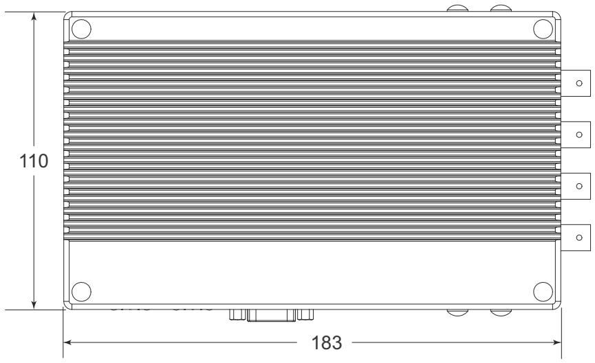
![110\n183](.mcm-100-102-50-1z298-1000-10/5ddd9f499a436fff809b261b2c9cd94073fddd31ccbcca05056186fd1ac33723.jpg)

Figure 1-1: Top View (MCM-100)

![U8 U2 U1 COM1\nCOM2\nADLINK\n84](.mcm-100-102-50-1z298-1000-10/12466d9959e1648f7a9859720b5f20a1f46af532352b3d3265b06601adbc003d.jpg)

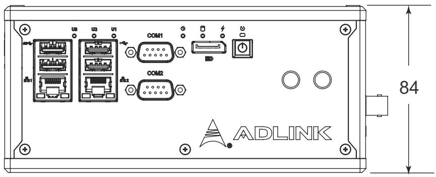
Figure 1-2: Front View

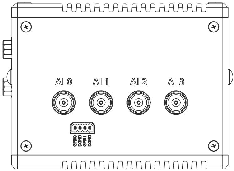
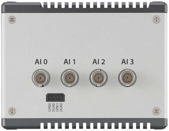
![AI 0\nAI 1\nAI 2\nAI 3\nGP00\nDGND\nGP01\nDGND](.mcm-100-102-50-1z298-1000-10/a314127ea1edaa95a2bc7275d802106c4bd48441fe7be66f98b74a7175da42f5.jpg)

Figure 1-3: MCM-100 (Right) Side View
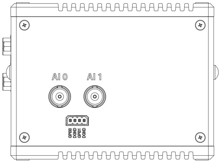
![AI 0\nAI 1\nGP00\nDGND\nGP01\nDGND](.mcm-100-102-50-1z298-1000-10/778b5b7e8a5b414e8a509ac60282ac806d6608237d044d4912c2254407ffc208.jpg)

Figure 1-4: MCM-102 (Right) Side View
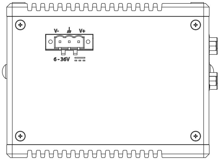
![V-\nV+\n6 - 36V\n---](.mcm-100-102-50-1z298-1000-10/5acd06c3ccd4078449fc656594388eb3604d67030b6fea625e8e33edb9bcabf7.jpg)

Figure 1-5: (Left) Side View

# 1.4 I/O Connectors

The following lists I/O connectors of the MCM-100/102, as labeled.
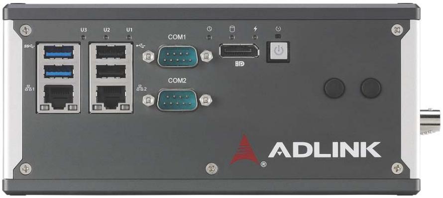
![U3 U2 U1\nSS\nDS1\nCOM1\nBD\nCOM2\nDS2\nADLINK®](.mcm-100-102-50-1z298-1000-10/68d46c11221aa448536badd7935a3b8d544fa9524de0ed0a2590a80ca855d88f.jpg)

Figure 1-6: Front Panel I/O

![AI 0\nAI 1\nAI 2\nAI 3\nGP00\nDGND\nGP01\nDGND](.mcm-100-102-50-1z298-1000-10/bff3a9a9967304057b01a65a66e0fab396f734117cb8c4ee9ea8b59f3a6ce274.jpg)

Figure 1-7: MCM-100 Right Side Panel I/O
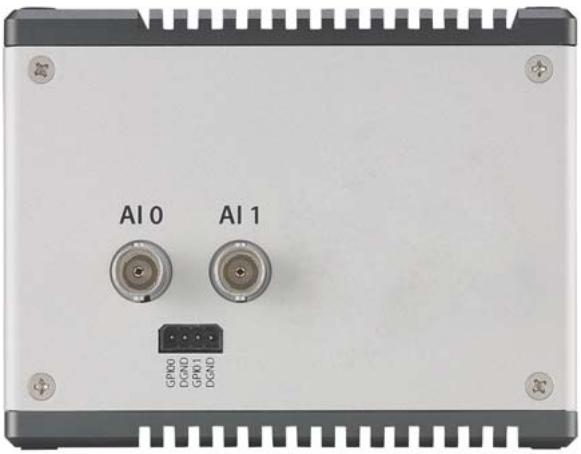
![AI 0\nAI 1\nGP00\nDGND\nCP01\nDGND](.mcm-100-102-50-1z298-1000-10/320e0847ca5ed845157d0af77f491acf325d4f44ba2f2e5cbec542a68080d0f9.jpg)

Figure 1-8: MCM-102 Right Side Panel I/O
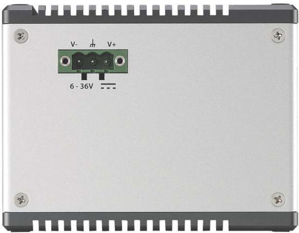
![V- m V+\n6 - 36V --](.mcm-100-102-50-1z298-1000-10/5b5b5cc8200341d1f80034e1c06cb01f31f676a0645b5c46523b3e360207057b.jpg)

Figure 1-9: Left Side Panel I/O

 Power button
 Reset button
 Antenna port
 DisplayPort connector
 LED operation indicators (x3)
 LED user-defined indicators (x3)
 DB-9P COM ports (x2)
 GbE ports (x2)
 USB2.0 ports (x2)
 USB3.0 ports (x2)
 BNC (x4)
 4-pin GPI/O w/ DGND
 DC power supply connector

# 1.4.1 Power Button

A non-latched push button with blue LED indicator. System is turned on when pressed, and the power LED lit. If the system hangs, depressing the button for 5 seconds powers down the system.

# 1.4.2 Reset Button

The reset button executes hard reset for the MCM-100/102.

# 1.4.3 DisplayPort Connector

One DisplayPort connector on the front panel supports the DP1.2 standard specification, and can connect to VGA, DVI, HDMI, and Display Port monitors via DisplayPort to VGA adapter cable, DisplayPort to DVI adapter cable, or DisplayPort to HDMI adapter cable and Display Port cable, with DP1.2 support for resolutions up to 4096 x 2160 at 60Hz.
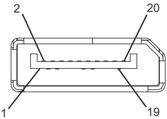
![2\n20\n1\n19](.mcm-100-102-50-1z298-1000-10/5051b8db194d7ab56d5d6ca9cbd4bacaa0de022bbbd119fc3a71e7a6909d67fe.jpg)

<table><tr><td>Pin</td><td>Signal</td><td>Pin</td><td>Signal</td></tr><tr><td>1</td><td>ML_Lane0_P</td><td>11</td><td>GND</td></tr><tr><td>2</td><td>GND</td><td>12</td><td>ML_Lane3_N</td></tr><tr><td>3</td><td>ML_Lane0_N</td><td>13</td><td>Config1</td></tr><tr><td>4</td><td>ML_Lane1_P</td><td>14</td><td>Config2</td></tr><tr><td>5</td><td>GND</td><td>15</td><td>Aux_P</td></tr><tr><td>6</td><td>ML_Lane1_N</td><td>16</td><td>GND</td></tr><tr><td>7</td><td>ML_Lane2_P</td><td>17</td><td>Aux_N</td></tr><tr><td>8</td><td>GND</td><td>18</td><td>Hot Plug</td></tr><tr><td>9</td><td>ML_Lane2_N</td><td>19</td><td>Return</td></tr><tr><td>10</td><td>ML_Lane3_P</td><td>20</td><td>DP_PWR_+3.3V</td></tr></table>

Table 1-1: DisplayPort Pin Assignment

# 1.4.4 LED Indicators

In addition to the LED of the power button, three LEDs on the front panel indicate the following operations.

<table><tr><td>Indicator</td><td>Color</td><td>Description</td></tr><tr><td>Watchdog (WDT)</td><td>Yellow</td><td>Indicates watchdog timer status. Flashes when watchdog timer starts, and when timer is expired, system will auto-reboots.</td></tr><tr><td>HDD</td><td>Red</td><td>When blinking, indicates the SATA hard driver is active</td></tr><tr><td>Standby</td><td>Blue</td><td>Indicates the system is in power standby mode</td></tr></table>

Table 1-2: LED Operation Indicators

# 1.4.5 DB-9P COM Port Connector

Through D-sub 9-pin connectors, COM1 and COM2 support RS-232, RS-422, and RS-485 modes by BIOS setting.

![1\n5\n6\n9](.mcm-100-102-50-1z298-1000-10/7ddb1682b65f66716d0a3913ef7e415d4fcfb03ef0d5bf925cc81c226fa0176f.jpg)

Figure 1-10: DB-9P COM Port

<table><tr><td>Pin</td><td colspan="3">Signal</td></tr><tr><td></td><td>RS-232</td><td>RS-422</td><td>RS-485</td></tr><tr><td>1</td><td>DCD#</td><td>TXD422-</td><td>485-</td></tr></table>

Table 1-3: DB-9P COM Port Pin Assignment

<table><tr><td>Pin</td><td colspan="3">Signal</td></tr><tr><td>2</td><td>RXD</td><td>TXD422+</td><td>485+</td></tr><tr><td>3</td><td>TXD</td><td>RXD422+</td><td>N/C</td></tr><tr><td>4</td><td>DTR#</td><td>RXD422-</td><td>N/C</td></tr><tr><td>5</td><td>GND</td><td>N/C</td><td>N/C</td></tr><tr><td>6</td><td>DSR#</td><td>N/C</td><td>N/C</td></tr><tr><td>7</td><td>RTS#</td><td>N/C</td><td>N/C</td></tr><tr><td>8</td><td>CTS#</td><td>N/C</td><td>N/C</td></tr><tr><td>9</td><td>RI#</td><td>N/C</td><td>N/C</td></tr></table>

Table 1-3: DB-9P COM Port Pin Assignment

# 1.4.6 Dual Gigabit Ethernet Ports

Two Gigabit Ethernet ports on the front panel support the Intel i210IT GbE controller, which provides:

 IEEE 802.3az Energy Efficient Ethernet
 IEEE 1588/802.1AS precision time synchronization
 IEEE 802.3av traffic shaper
 Interrupt moderation, VLAN support, IP checksum offload
 PCIe OBFF (Optimized Buffer Flush/Fill) for improved system power management
 Four transmit and four receive queues
 RSS and MSI-X to lower CPU utilization in multi-core systems
 ECC - error correcting memory in packet buffers
 Wake-On-LAN
 NC-SI for greater bandwidth passthrough
 Preboot eXecution Environment (PXE) flash interface support
 Jumbo frame support

<table><tr><td>LED</td><td>LED Color</td><td>Status</td><td>Description</td></tr><tr><td rowspan="3">Active/Link</td><td rowspan="3">Yellow</td><td>OFF</td><td>Ethernet port is disconnected</td></tr><tr><td>ON</td><td>Ethernet port is connected with no activity</td></tr><tr><td>Flashing</td><td>Ethernet port is connected and active</td></tr><tr><td rowspan="3">Speed</td><td rowspan="3">Green/Yellow</td><td>OFF</td><td>10 Mbps</td></tr><tr><td>Green</td><td>100 Mbps</td></tr><tr><td>Yellow</td><td>1000 Mbps</td></tr></table>

Table 1-4: Gigabit Ethernet Port LED Function

# 1.4.7 USB 3.0 Port

The USB 3.0 port supports Type A connection, compatible with SuperSpeed, Hi-Speed, full-speed and low-speed USB devices, with support for multiple boot devices, including USB flash, USB external HDD, and USB CD-ROM drivers and boot priority and boot device configured in BIOS.

![The image depicts a white document icon featuring a folded top-right corner and faint horizontal lines across the lower half. A large, bold red checkmark is superimposed diagonally over the center of the page.](.mcm-100-102-50-1z298-1000-10/f20dd887f145cd8d81c0f0467e9058a58359de450f8c35baa8e413f26f5cf496.jpg)
NOTE:

When using USB CD-ROM via USB 3.0 port to re-install or repair the OS, cold boot should be utilized

# 1.4.8 BNC Connectors

Four BNC connectors are located on the right side of the MCM-100, and two are located on the right side of the MCM-102.

![Technical diagram of a circular component with polarity indicators and center mark](.mcm-100-102-50-1z298-1000-10/2dfc5f6b1cf318ab08aab8cddbcb7798c329a9479dfd82d2e4349db419345a7a.jpg)

Figure 1-11: BNC Connector Polarity

# 1.4.9 4-pin GPI/O w/ DGND Connector

The 4-pin removable spring terminal connector provides connection for GPI/O0, GPI/O1, and two DGND signals

![GPIO0\nDGND\nGPIO1\nDGND](.mcm-100-102-50-1z298-1000-10/3ffee14238ada906c8226cd5e2bcaea38d127c702672b2a66123bb11b06d6e84.jpg)

Figure 1-12: 4-pin GPI/O w/ DGND Connector

# 1.4.10 DC Power Supply Connector

Located on the left side panel.

![V-\nV+\n6V-36V DC IN](.mcm-100-102-50-1z298-1000-10/5443d62003398a08b2b2204829e4b14311a031b23532da39ceb426e28733d177.jpg)

Figure 1-13: DC Power Connector

# 1.5 Adapters and Other Accessories

Device adaptors and other optional accessories should only be obtained through your ADLINK dealer. For more information, see “Getting Service” on page 101.

This page intentionally left blank.

# 2 Getting Started

# 2.1 Unpacking Checklist

Before unpacking, check the shipping carton for any damage. If the shipping carton and/or contents are damaged, inform your dealer immediately. Retain the shipping carton and packing materials for inspection. Obtain authorization from your dealer before returning any product to ADLINK. Ensure that the following items are included in the package.

 MCM-100/102 unit
 DIN rail brackets
 Wall mounting kit
 Screw pack for DIN rail, wall mounting, and storage fixing
 Quick Start Guide

# 2.2 Connecting DC Power

![The image displays a maroon triangular warning symbol featuring a white exclamation point in the center. Below the triangle, the word 'WARNING:' appears in black capital letters.](.mcm-100-102-50-1z298-1000-10/683c18699adf707ef6029749c18c0d8a0eed0c494a58463f04fd6f4b7c8c2ebf.jpg)

Before providing DC power to the MCM-100/102, ensure the voltage and polarity provided are compatible with the DC input. Improper input voltage and/or polarity can be responsible for system damage.

Active DC power sources must comply with LPS and SELV circuits with no energy hazard, as well as the following.

 IEC 60950-1:2005+A1:2009+A2: 2013
 Output voltage: 6 to 36VDC
 Output current: 4.2 to 0.7A minimum
 Tma: $5 0 ^ { \circ } \mathrm { C }$ min.

The DC power input connector of the MCM-100/102 utilizes V+, Vand chassis ground pins, and accepts input voltage as shown previously.

# 2.3 DIN Rail Mounting

The MCM-100/102 controller is shipped with wall-mounting brackets and accessory screws, with mounting procedures as follows.

1. Prepare the DIN rail mounting bracket and 2 M4-F head screws.

![Close-up of a mechanical component with two red-circled holes, no visible text or symbols](.mcm-100-102-50-1z298-1000-10/72bff56eb6b1f1970ca3638bde008a2115dfa17713aab22f063f70a215d77b63.jpg)

2. Use the 2 included M4-F head screws to fix the DIN rail bracket to the chassis, according to the spacing dimensions of the screw holes and brackets, as shown.

![60.6\n113.95\n118.22\n134.3\n150.38\n161.58](.mcm-100-102-50-1z298-1000-10/da12fcebd2cca3a89a066bec31b9b4e0958b96cb96170509eb6e0c11975ac960.jpg)

# 2.4 Wall Mounting

The MCM-100/102 ships with wall-mounting brackets and accessory screws, with mounting procedures as follows.

![The image displays a yellow triangular warning sign with a thick black border. Inside the triangle is a large black exclamation point. Below the triangle is a white rectangular label containing the text 'CAUTION:' in black capital letters.](.mcm-100-102-50-1z298-1000-10/7ff40bccd5304606f265849db455debc80b7707ea2e70f23443181adbdcfbb0e.jpg)

While configuration shown may indicate otherwise, due to the presence of antenna ports, for safety, the device should ONLY be wall-mounted with the front and rear panels on the sides, NEVER on the top or underside.

Use the 4 M4 screws to fix the 2 wall-mount brackets to the chassis, according to the spacing dimensions of the screw holes and brackets. The MCM-100 is shown as an example.

![ADLINK](.mcm-100-102-50-1z298-1000-10/4bb87e5524b8a4831048af4bd93bae7891f9e59b4877d3af64dcf17e93e9a67b.jpg)

![149\n113\nØ4.5\nØ5.2\n97\n134\n152.4\nR5](.mcm-100-102-50-1z298-1000-10/d1e7611be4130d59df055cc6dcb639f541e1c111b561816e9583b943b5ea4a81.jpg)

# 2.5 Cooling Considerations

Heat-generating components of the MCM-100/102 (such as CPU and PCH) are all situated on the left side of the system. These components directly contact the heat sink via thermal pads and dissipate heat generated by the components. To maximize efficiency of heat dissipation, maintain a minimum of 2 inches (5cm) clearance on the top of the MCM-100/102.

# 2.6 Installing Mini-PCIe WiFi Module (Optional)

1. Remove all screws and internal mini-USB connector, separating the MCM-100/102 into five parts.

![Disassembled electronic device components including a circuit board, power connectors, and a connected module on a pink surface (no visible text or symbols)](.mcm-100-102-50-1z298-1000-10/95f60d8c9de9d0935991daeb9fff6d13c5d92341d5aa80632a790b47c6f00cfc.jpg)

2. Fix bracket with two screws.

![B02.11ac RTL8812AEBT MiniCard Made in TA5WAN\nModel:RTL8812AEACC RTL8812AEACC 01\nFCC ID:TK2 RTL8812AEBT\nIC:6317A RTL8812AEBT\nWLAN MAC: B01F81D41C52\nBT MAC: B01F81D42422\n©F4 94V-0 F135 HM812A03-3V9](.mcm-100-102-50-1z298-1000-10/d96a6ce8994d6a599f692fb79ce9c89e0221a1a0f7f1495dbe5753cd4cd3ca5b.jpg)

3. Insert mini-PCIe WiFi module into the carriage at an angle.

![Interior view of an electronic circuit board with visible components and a red annotation box highlighting a component (no readable text or symbols)](.mcm-100-102-50-1z298-1000-10/5c655b1f613b31e3c8e31c2f23fbe578c72fda2fe8b1d9be7c8d28f5476edd3f.jpg)

4. Depress the module until seated and fix with two M2.5- P-head-L5 screws.

![Interior view of an electronic circuit board with visible components and connectors (no readable text or symbols)](.mcm-100-102-50-1z298-1000-10/fce467a2c69e29d2a52596e81200994ff619bf0faf0516d3906fd3eeb89e9847.jpg)

5. Connect SMA-to-IPEX cable to WiFi module.

![Interior view of an electronic circuit board with visible components and wiring, no readable text or symbols present.](.mcm-100-102-50-1z298-1000-10/80b9bc3056359021df4b947637d025fc82187d0026c1870e8c92ea21b89d339d.jpg)

6. Remove plastic cap and mount SMA connectors.

![Close-up of a gloved hand installing a gold-colored connector into a black hard drive on a pink textured surface (no text or symbols visible)](.mcm-100-102-50-1z298-1000-10/b50584b6f1c3e3f41f75ab12bea3683bf6983d3c1769f162a6d39179e2e41cdc.jpg)

7. Reassemble all parts and connect mini-USB, fixing the chassis with screws.

![Interior view of an open electronic device showing internal components like circuit boards, RAM slots, and a black plastic connector (no text or symbols visible)](.mcm-100-102-50-1z298-1000-10/da3ef9c3e0b02538da74cb54422711bb543d111840d804e19742542a7b686c1c.jpg)

8. Connect antenna to SMA connector

![Close-up of a white electronic device with two black antennas attached to its side, placed on a pink fabric background (no visible text or symbols on the device body beyond labels)](.mcm-100-102-50-1z298-1000-10/a8cc5e4ac9d7bee752f8f1782303637386e329666e9a5f39b523979cbb7d518f.jpg)

This page intentionally left blank.

# 3 Driver & Application Installation

After installing the operating system, all related drivers must be installed for the system to function properly. This section describes the drivers needed for Windows operating systems and the procedures to install them. For other OS support, please contact ADLINK for further information.

Install drivers as follows.

1. Fully install Microsoft Windows OS before installing any drivers. Most standard I/O device drivers have been included in Microsoft Windows OS. For Windows 10 IoT Enterprise users, please note that you need Administrator privilege to install the drivers properly.
2. Install the chipset driver.
3. Install the graphics driver.
4. Install the Ethernet driver.
5. Install the USB 3.0 driver
6. Install the I/O controller
7. Install the SEMA utility, WDT and DI/O drivers.
8. Install AI and DI/O drivers

# 3.1 Installing the Chipset Driver

The chipset driver directs the operating system to configure the Intel® chipset components in order to ensure that the following features function properly:

 SATA Storage Support
 USB Support
 Identification of Intel® Chipset Components in the Device Manager

Windows 10 IoT Enterprise must be fully installed and running on the system before installing this software:

To install the chipset driver for the MCM-100/102

1. Close any running applications.
2. From ADLINK's website, download Windows 10 IoT Enterprise drivers for the MCM-100/102.
3. Execute Setup.exe and follow onscreen instructions to complete the setup.
4. After installation is complete, reboot the system.

# 3.2 Installing the Graphics Driver

The MCM-100/102 is equipped with the Intel® Graphics Media Accelerator Driver package, which supports Windows 10 IoT Enterprise.

To install the graphics driver:

1. Close any running applications.
2. From ADLINK's website, download Windows 10 IoT Enterprise drivers for the MCM-100/102.
3. Execute Setup.exe and follow onscreen instructions to complete the setup.
4. After installation is complete, reboot the system.

# 3.3 Installing the Ethernet Driver

To install the driver for the Intel I210 Gigabit Ethernet controller:

1. Close any running applications.
2. From ADLINK's website, download Windows 10 IoT Enterprise drivers for the MCM-100/102.
3. Execute autorun.exe and follow onscreen instructions to complete the setup.
4. After installation is complete, reboot the system.

# 3.4 Installing the USB 3.0 Driver

To install the driver for the USB 3.0 controller:

1. Close any running applications.
2. From ADLINK's website, download Windows 10 IoT Enterprise drivers for the MCM-100/102.
3. Launch setup.exe and follow onscreen instructions to complete the setup.
4. After installation is complete, reboot the system.

# 3.5 Installing the I/O Controller Driver

To install the driver for the I/O controller:

1. Close any running applications.
2. From ADLINK's website, download Windows 10 IoT Enterprise drivers for the MCM-100/102.
3. Execute setup.msi and follow onscreen instructions to complete the setup.
4. After installation is complete, reboot the system.

# 3.6 Installing the SEMA Utility, WDT and DI/O Drivers

The MCM-100/102 supports ADLINK Smart Embedded Management Utility with features as follows.

 System Health for real time CPU, system temperature, total/ current uptime
 User-defined 1KB Flash
 Watchdog Timer
 Hardware Monitoring for input voltage levels and current power consumption

A WDT (watchdog timer) is a hardware mechanism resetting the system when the operating system or application is halted. A typical usage of WDT is to start the timers and periodically reset the timer, and when timer is expired, the system resets. SEMA utility installation is required to access the WDT function.

To install the SEMA utility, WDT and DI/O drivers:

1. Close any running applications.

From ADLINK's website, download Windows 10 IoT Enterprise drivers for the MCM-100/102.

2. Execute Setup.exe and follow onscreen instructions to complete the setup.

After installation is complete, reboot the system.

![The image displays a simple icon of a white document or piece of paper. The top-right corner is folded down. Faint grey horizontal lines run across the lower portion, suggesting text. A large, bold red checkmark is superimposed diagonally over the center of the document.](.mcm-100-102-50-1z298-1000-10/880d93648b06ff4ab3f322c12b04603d7fc03e2d0fb0822dfc064ebe184622b7.jpg)
NOTE:

Administrator privilege is required to use the API in Windows 10 IoT Enterprise.

Complete document support for SEMA utility can be found at:

https://www.adlinktech.com/Products/

Industrial\_IoT\_and\_Cloud\_solutions/

SEMA\_Smart\_Embedded\_Management\_Agent/SEMA?lang=en

# 3.7 Installing AI and DI/O Drivers

# MAPS Core

MAPS Core utilizes advanced 32/64-bit kernel drivers for customized DAQ application development. MAPS Core enables detailed operations for superior performance and reliability from data acquisition systems. MAPS kernel drivers now support Windows 7/10 OS.

![The image displays a graphic icon of a white document or notepad with the top-left corner folded down. Horizontal gray lines run across the lower portion, simulating text. A large, bold red checkmark is superimposed over the document, slanting upwards from the bottom left to the top right.](.mcm-100-102-50-1z298-1000-10/8874a7b5f2e823bca3178a0b6f975c49b4b5197cccbfd63fcbf5799e995acec4.jpg)
NOTE:

Only MAPS Core versions 18.10 and later are supported by the MCM-100/102.

Install the MAPS Core Installer Suite, available for download from the ADLINK website.

# DAQ-LVIEW Plus

The task-oriented SDK supports LVOOP VI and Polymorphic VI for LabVIEW.

Download DAQ-LVIEW Plus from the ADLINK website.

This page intentionally left blank.

# 4 Operation

Operation of the MCM-100/102 is described here to assist in configuration and programming of the module. Functions addressed include analog input and GPI/O.

# 4.1 Analog Input

# 4.1.1 Analog Input Front End Configuration

![The flowchart depicts a sequential signal processing path from left to right:\n\n1.  **Input:** An arrow labeled **'AI'** points into the first block.\n2.  **Block 1:** A beige rectangle labeled **'Calibration Circuit'**.\n3.  **Connection:** An arrow points to the next block.\n4.  **Block 2:** A beige rectangle labeled **'Differential/ Psuedo-differential Switch Circuit'** (note the spelling of 'Psuedo').\n5.  **Connection:** An arrow points to the next block.\n6.  **Block 3:** A beige rectangle labeled **'IEPE Circuit'**.\n7.  **Connection:** An arrow points to the next block.\n8.  **Block 4:** A beige rectangle labeled **'AC Coupling circuit'** (note the lowercase 'c').\n9.  **Connection:** An arrow points to the next block.\n10. **Block 5:** A light blue triangle labeled **'ADC Driver'**.\n11. **Connection:** Two pink arrows point to the final block. The top arrow is labeled above with **'Diff input'**.\n12. **Block 6:** A large pink trapezoid labeled **'24 Bit ADC'**.](.mcm-100-102-50-1z298-1000-10/00554cdfc392fd957e7ea8cc8a5c5a761d5bd06b28d67434f00e7916f077f49e.jpg)

Figure 4-1: MCM-100/102 Analog Front End

# Input Configuration: Differential/Pseudo-Differential

Differential input mode provides anode and cathode inputs of the BNC connector that respond to signal voltage differences therebetween. If the signal source is ground-referenced, the differential input mode can be used for common-mode noise rejection.

If the signal source is a floating signal, setting pseudo-differential input mode will provide a reference ground connected to the cathode input of the BNC through a 20 kΩ resistor.

Recommended configurations for the signal sources are as follows.

<table><tr><td>Signal Source</td><td>Card Configuration</td></tr><tr><td>Floating</td><td>Pseudo-differential</td></tr><tr><td>Ground-reference</td><td>Differential</td></tr></table>

Table 4-1: Signal Source-Card Configuration

# Input Coupling

When DC coupling is selected, DC offset present in the input signal is passed to ADC. DC coupling configuration is indicated when the signal source has a small offset voltage or if the DC content of the signal is important. When AC coupling is selected, DC offset present in the input signal is removed. AC coupling configuration is indicated when the DC content of the input signals is to be rejected. AC coupling enables a high pass R-C filter through the input signal path, with corner frequency (-3dB) about 0.4 Hz.

# IEPE Input

For applications utilizing sensors such as accelerometers or microphones, the MCM-100/102 provides an excitation current source.

The excitation current is 2 mA for the IEPE sensors, with DC voltage offset generated because of the excitation current and sensor impedance. When enabling IEPE current sources, the MCM-100/ 102 automatically sets input configuration to AC coupling.

![Based on the provided image, here is an accurate and concise description of the flowchart:\n\n**Blocks and Labels:**\n*   **IEPE Sensor** (inside a dotted box on the left)\n*   **AI Channel** (above a circle symbol in the center)\n*   **VCC** (at the top right)\n*   **2mA Constant Current** (next to a current source symbol)\n*   **IEPE ON/OFF** (next to a switch symbol)\n*   **MCM-100 Analog Front End** (inside a solid box on the right)\n\n**Connections:**\n1.  Inside the **IEPE Sensor** box, a piezoelectric element (represented by stacked blue and white rectangles) is grounded and connects to the input of an amplifier (triangle). The amplifier output connects to the **AI Channel**.\n2.  The **AI Channel** (a circle with an inner circle and ground connection) receives the signal and passes it to the right into the **MCM-100** section.\n3.  Inside the **MCM-100 Analog Front End** box:\n    *   **VCC** connects to a current source symbol labeled **2mA Constant Current**.\n    *   This current source connects via a switch labeled **IEPE ON/OFF** to the main signal line coming from the AI Channel.\n    *   The signal line continues to the right through a capacitor and connects to the input of a final amplifier (triangle).](.mcm-100-102-50-1z298-1000-10/cdc539334e3605ad02c4d203152b0bd6a0813a56ba9942bf2885dc6b7cb1cc5b.jpg)

Figure 4-2: Excitation Current for IEPE Sensor Measurement

# 4.1.2 AI Data Format

When an A/D converter is used, properties of the signal to be measured must be ascertained to determine the channel to be used and connections to the card. After A/D conversion, the A/D data is buffered in a Data FIFO, for transfer to memory for further processing. Transfer characteristics of various input ranges of the MCM-100/102 are as follows, with data format 2’s complement.

<table><tr><td>Description</td><td>Bipolar Analog Input Range</td><td>Digital Code</td></tr><tr><td>Full-scale Range</td><td>±10V</td><td></td></tr><tr><td>Least significant bit</td><td>1.19uV</td><td></td></tr><tr><td>FSR-1LSB</td><td>9.99999881V</td><td>7FFFFFFh</td></tr><tr><td>Midscale +1LSB</td><td>1.19uV</td><td>000001h</td></tr><tr><td>Midscale</td><td>0V</td><td>000000h</td></tr><tr><td>Midscale -1LSB</td><td>-1.19uV</td><td>FFFFFFh</td></tr><tr><td>-FSR</td><td>-10V</td><td>800000h</td></tr></table>

Table 4-2: MCM-100/102 Input Ranges

# 4.1.3 Sampling Rate

To drive the sigma-delta ADC, an onboard timebase clock is applied, with frequency exceeding the sampling rate, produced from a DDS (Direct Digital Synthesis) chip. The output frequency of the DDS chip is programmable, with excellent resolution.

DDS Timing/Sampling Rate

<table><tr><td>Mode</td><td>High Resolution</td><td>High Speed</td></tr><tr><td>Sampling Rate</td><td>1 kHz ~ 52.734 kHz</td><td>52.734 kHz ~ 128 kHz</td></tr><tr><td>fCLK/fDATA</td><td>512</td><td>256</td></tr><tr><td>DDS CLK</td><td>512kHz to 26.999808MHz</td><td>13.499904 MHz to 2.768 MHz</td></tr><tr><td>Sampling Rate Resolution</td><td>0.0003 Hz</td><td>0.0003 Hz</td></tr></table>

# 4.1.4 Data Transfer

# Software Polling Data Transfer (Non-Buffering Programmed I/O)

Polling mode supports flexible timing and is suitable for retrieving recent data without FIFO buffering latency. The MCM-100/102 continuously updates the most recently acquired data onto a data port for specific channels. Data not retrieved in time is overwritten with new data without notification. The UD-DASK Function Library Reference provides corresponding software API details.

# Continuous Acquisition Mode

Differs from software polling mode only in the generation of block data in continuous acquisition mode without the need to consider data overwriting or acquiring repeat data in software polling mode. This mode is suitable for when continuous data is to be acquired in a fixed and precise time interval. Please note the data buffer size must be a multiple of 256 in continuous acquisition mode. The UD-DASK Function Library Reference provides corresponding software API details.

# 4.1.5 Anti-Aliasing Filter and Frequency Response

The filter limits the bandwidth of the signal path and rejects out-ofband noise. The digital filter of the Sigma-Delta ADC sets the overall frequency response, using multi-stage FIR topology to provide linear phase with minimal passband ripple and high stopband attenuation. These image frequencies, if present in the signal and not externally filtered, will fold back (or alias) into the passband, causing errors. The stopband of the ADC provides 100dB attenuation of frequencies that begin just beyond the passband and continue out to ADC over-sampling rate. The MCM-100/102 provides an anti-aliasing, low-pass, simple RC filter in front of the ADC inputs to limit possible high amplitude out-of-band signals and noise.

![| Input Signal Frequency (kHz) | -3dB Bandwidth (dB) |\n| ---------------------------- | ------------------- |\n| 25                           | -2.058              |](.mcm-100-102-50-1z298-1000-10/7f609e226b1e76f1633d4c90907972c3a04057ee67d4417413c26720a64020d9.jpg)

Figure 4-3: Input Frequency Response for High Resolution Mode

![| Input Signal Frequency (kHz) | -3dB Bandwidth (dB) |\n| ---------------------------- | ------------------- |\n| 50                           | -2.27               |](.mcm-100-102-50-1z298-1000-10/b23020f1a164fbfff22486f9d51a882c6c7ff7030614d45c4396e04fe2bda415.jpg)

Figure 4-4: Input Frequency Response for High Speed Mode

# 4.2 Triggering

The MCM-100/102 supports flexible trigger sources and trigger modes for analog input functionality. The trigger source can originate with software command, external analog, or external digital signal in continuous analog input mode. Trigger source and mode are programmable by software.

# 4.2.1 Analog Input Trigger Source

# Software Triggering

This trigger mode requires no external trigger signals. The trigger asserts immediately following execution of the specified function calls to begin the operation.

# External Analog Trigger

The analog multiplexer can select one input channel as the analog trigger source. That is, one of 4 input channels can be selected as the analog trigger source. An external analog trigger occurs when the analog trigger signal crosses above (above high) or below (below low) the pre-defined voltage level. The range of trigger level is the full-scale range of the selected input channel and the resolution is 24-bit. In external analog trigger mode, the first acquired data starts with a delay time of 1/(sampling rate).

# Below-Low Analog Triggering

As shown, the trigger signal is generated when the input analog signal is less than the Low\_Threshold voltage. High\_Threshold setting is not used in this triggering situation.

![| Time Segment | Value |\n| ------------ | ----- |\n| Low Threshold | Low Threshold |\n| Trigger      | Trigger (boxed) |](.mcm-100-102-50-1z298-1000-10/e1f028b8b745abaa93328f97d7e47591d004953fa7a8351777d34b2014b6708d.jpg)

Figure 4-5: Below-Low Analog Triggering

# Above-High Analog Triggering

As shown, the trigger signal is generated when the input analog signal exceeds the High\_Threshold voltage. Low\_Threshold setting is not used in this triggering situation

![| Time Segment | Value |\n| ------------ | ----- |\n| High Threshold | High_Threshold |\n| Trigger      | Trigger (approx) |](.mcm-100-102-50-1z298-1000-10/8b231138e1e73896c72b02e13ba479e2b62f0b195dc2917472afcd4e3ac0dc81.jpg)

Figure 4-6: Above-High Analog Triggering

# External Digital Triggering

An external digital trigger occurs when a rising or falling edge is detected on the digital signal connected to the GPI/O pin. Trigger polarity can be programmed using ADLINK software drivers.

![The image depicts an icon of a white piece of lined paper with a folded corner in the top right. A large, bold red checkmark is superimposed diagonally over the document.](.mcm-100-102-50-1z298-1000-10/e6c13035a3c6d3b4023660e9f1513c3e123a37f14470a7e0aad1f66a6c1c95f2.jpg)
NOTE:

Signal level of the external digital trigger signals should be 3/ 3V/TTL-compatible, with a minimum pulse of 20ns.

![Positive-edge\n(rising) trigger event\noccurs\nNegative-edge\n(falling) trigger\nevent occurs](.mcm-100-102-50-1z298-1000-10/b45c95b9cc8ce92ec86b9c22da066b7604d415d422bb29e849c8eb8bd9965e25.jpg)

Figure 4-7: Digital Triggering

# Trigger Modes

Analog input supports post, delay, middle, gate, post trigger with retrigger, and delay trigger with retrigger modes.

# Post-Trigger Acquisition Mode (no retrigger)

Post-trigger acquisition is indicated in applications where data is to be collected after a trigger event, as shown.

![The diagram illustrates a timeline of data acquisition events and signals:\n\n*   **Timeline:** A horizontal line labeled **Time** at the far right.\n*   **Event Markers:** Three text blocks with downward arrows pointing to the timeline:\n    *   **Operation start**\n    *   **Trigger Event Occurs** and **Acquisition start**\n    *   **Acquisition stop** and **Begin to transfer data to system**\n*   **Signals:** Two rows below the timeline:\n    *   **Trigger:** A waveform showing a brief square pulse that aligns vertically with the **Trigger Event Occurs** event.\n    *   **Data:** A waveform showing a long rectangular block labeled **N samples**. This block begins at the rising edge of the **Trigger** pulse and ends at the **Acquisition stop** event.](.mcm-100-102-50-1z298-1000-10/678a2147757d050b8e2b07464e314e460f27d123e23251a42b0b4f268e09b01e.jpg)

Figure 4-8: Post Trigger without Retrigger

# Pre-trigger Acquisition (no retrigger)

Collects data before the trigger event, with acquisition starting once specified function calls are executed to begin the pre-trigger operation, and stopping when the trigger event occurs. If the trigger event occurs after the specified amount of data has been acquired, the system stores only data preceding the trigger event by a specified amount, as shown. Note that N must be equal to or less than 8k samples for all analog input channels.

![This diagram illustrates a data acquisition timeline and buffering process.\n\n**Timeline and Events:**\n*   A horizontal arrow labeled **Time** runs across the top.\n*   A left-pointing arrow marks the start of the process with the text:\n    *   **Operation start**\n    *   **Acquisition start**\n*   A right-pointing arrow marks the end of the process with the text:\n    *   **Trigger Event Occurs**\n    *   **Acquisition stop**\n    *   **Begin to transfer data to system**\n\n**Signal and Data Buffer:**\n*   Below the timeline is a line labeled **Trigger**, showing a square pulse aligned with the second event on the timeline.\n*   Below that is a line labeled **Data**, pointing to a long rectangular buffer bar.\n    *   The left portion of the bar is filled with diagonal hatching. A bracket below it reads: **This data is discarded.**\n    *   The right portion of the bar is labeled **N samples**. A bracket below it reads: **Only acquired N samples will be transferred back to system.**](.mcm-100-102-50-1z298-1000-10/38dc3aa252b12cfd7d34c7137a0caf199f95327d532d9c4be7fd01f2de714c8c.jpg)

Figure 4-9: Pre-trigger Mode Operation (valid trigger only)

The trigger event occurs after the specified amount of data has been acquired. However, if the trigger event occurs before the specified amount of data has been acquired, the acquisition engine ignores the trigger signal until the specified amount of data has been acquired, as shown.

![Based on the provided image, here is an accurate description of the timing diagram:\n\n**Labeled Blocks and Text:**\n*   **Timeline:** A horizontal arrow labeled 'Time' pointing to the right.\n*   **Event Annotations:**\n    *   Left: '• Operation start', '• Acquisition start'\n    *   Middle: '• Trigger signals that occur before the specified amount of data has been acquired are ignored'\n    *   Right: '• Trigger Event Occurs', '• Acquisition stop', '• Begin to transfer data to system'\n*   **Signal Labels:** 'Trigger' and 'Data'.\n*   **Data Buffer Text:** 'N samples' and 'X samples have been acquired before trigger occurs, where X(N'.\n\n**Connections and Relationships:**\n*   **Timeline Events:** Three downward arrows point to specific points on the 'Time' line.\n    *   The left arrow marks the start.\n    *   The middle dotted arrow marks an intermediate point where early triggers are ignored.\n    *   The right arrow marks the final trigger event where acquisition stops.\n*   **Trigger Signal:** The 'Trigger' line shows a waveform with two square pulses.\n    *   The first pulse aligns vertically with the middle timeline event (the 'ignored triggers' text).\n    *   The second pulse aligns vertically with the right timeline event (the 'Trigger Event Occurs' text).\n*   **Data Acquisition:** The 'Data' line shows a horizontal bar divided into two sections aligned with the timeline above.\n    *   **Left Section:** A hatched (shaded) section. Below it, a dimension line indicates its width with the text: 'X samples have been acquired before trigger occurs, where X(N'. This section aligns vertically with the time period leading up to the second trigger pulse.\n    *   **Right Section:** A white section labeled 'N samples' that follows the hatched section.](.mcm-100-102-50-1z298-1000-10/e0d7395f5d24b2a16e29c2a3042e0aab1391e07a4724fd3c79d936e698bf637f.jpg)

Figure 4-10: Pre-trigger Mode Operation (w/ invalid trigger)

# Delay-Trigger Acquisition (no retrigger)

Delays data collection after the trigger event, as shown. The delay count is specified by a 32-bit counter value, such that the maximum delay count is $( 2 ^ { 3 2 } - 1 )$ when the minimum delay count is 1.

![Based on the provided image, here is an accurate and concise description of the diagram:\n\n**Timeline and Events**\nThe diagram is centered around a horizontal arrow pointing to the right, labeled **Time**. Along this timeline, specific events are marked by vertical arrows pointing downward:\n1.  **Operation start**\n2.  **Trigger Event Occurs**\n3.  **Acquisition start**\n4.  **Acquisition stop** / **Begin to transfer data to system** (These appear as a single label block with two bullet points).\n\n**Connections and Signals**\n*   **Delay Time:** A horizontal line labeled **Delay Time** connects the **Trigger Event Occurs** point to the **Acquisition start** point.\n*   **Trigger Signal:** Below the timeline, a trace labeled **Trigger** shows a single square pulse. This pulse is vertically aligned directly below the **Trigger Event Occurs** marker.\n*   **Data Signal:** Below the Trigger trace, a trace labeled **Data** features a long block labeled **N samples**. This block begins after the trigger event and ends at the **Acquisition stop** point, representing the duration of data acquisition.](.mcm-100-102-50-1z298-1000-10/c34df1571a4314b0f3683df7917bc4518fbca9e0c42b6a40e1b74969662c7ca2.jpg)

Figure 4-11: Delay-Trigger Mode Operation

# Middle-Trigger Acquisition

Middle-trigger acquisition is indicated when data is to be collected before and after the trigger event. The amount of stored data before and after trigger event can be set individually (M and N samples), as shown. Please note that M+N must be equal to or less than 8k samples for all analog input channels, and that the trigger event can only be accepted when the specified amount of data has been acquired (M samples), otherwise the trigger event will be ignored.

![Based on the provided diagram, here is the accurate description:\n\n**Labeled Blocks and Elements:**\n*   **Timeline:** A horizontal arrow labeled **'Time'** at the far right.\n*   **Events (Top):** Three downward-pointing arrows indicating specific moments on the timeline.\n    *   Left arrow labeled: **'Operation start'** and **'Acquisition start'**.\n    *   Middle arrow labeled: **'Trigger event occurs'**.\n    *   Right arrow labeled: **'Acquisition stop'** and **'Begin to transfer data to system'**.\n*   **Signal:** A line labeled **'Trigger'** displaying a square wave pulse.\n*   **Data:** A sequence labeled **'Data'** at the bottom consisting of three rectangular segments.\n    *   The first segment is a hatched/shaded block.\n    *   The second segment is labeled **'M samples'**.\n    *   The third segment is labeled **'N samples'**.\n\n**Connections and Relationships:**\n*   The arrow for **'Operation start'** and **'Acquisition start'** connects to the beginning of the timeline.\n*   The arrow for **'Trigger event occurs'** connects to the timeline and aligns vertically with the rising edge of the **'Trigger'** pulse and the start of the **'M samples'** block.\n*   The arrow for **'Acquisition stop'** and **'Begin to transfer data to system'** connects to the timeline and aligns vertically with the end of the **'N samples'** block.\n*   The **'Data'** blocks are arranged sequentially from left to right: the hatched block, followed by **'M samples'**, followed by **'N samples'**.](.mcm-100-102-50-1z298-1000-10/9a8bbaa16c03cb21053d847b730dc1e676c5dba851e68463b23dcc8ad59da943.jpg)

Figure 4-12: Middle-Trigger Acquisition

# Gated Trigger

Gated-trigger acquisition is indicated in applications where data is to be collected when trigger events are set to level high/low, and acquisition suspended when trigger events are set to the opposite level. The process repeats until the specified amount of data is acquired.

![The image is a timing diagram with three horizontal tracks aligned vertically:\n\n**1. Top Track (Timeline & Events):**\n*   A horizontal arrow pointing right labeled **'Time'**.\n*   Three downward arrows point to the timeline indicating specific moments:\n    *   Leftmost: Labeled **'Operation start'** and **'Acquisition start'**.\n    *   Middle: Labeled **'Trigger event occurs (high active)'**.\n    *   Rightmost: Labeled **'Trigger event occurs (high active)'**.\n\n**2. Middle Track:**\n*   Labeled **'Trigger'**.\n*   It shows a square wave signal that transitions to a high state corresponding to the 'Trigger event occurs' markers and returns to a low state between them.\n\n**3. Bottom Track:**\n*   Labeled **'Data'**.\n*   It displays a sequence of rectangular blocks aligned with the Trigger signal:\n    *   A hatched block (diagonal shading) starting at the 'Operation start'.\n    *   A white block labeled **'M samples'** aligned with the high period of the first Trigger pulse.\n    *   A hatched block aligned with the low period between pulses.\n    *   A white block labeled **'N samples'** aligned with the high period of the second Trigger pulse.\n    *   A hatched block aligned with the subsequent low period.\n    *   Ellipses **'....'** at the end indicating the pattern continues.](.mcm-100-102-50-1z298-1000-10/5f12bf02de1c41b6d2deeb5653ba819bed30d59b9cc2c70533d3f8dcd17ef4ca.jpg)

Figure 4-13: Gated Trigger

# Post-Trigger or Delay-Trigger Acquisition with Re-Trigger

Post-trigger or delay-trigger acquisition with re-trigger function is indicated in applications where data is to be collected after several trigger events. The number of scans after each trigger and the retrigger number are valid from 1 to the buffer size allocated in kernel space. The process repeats until the specified amount of retrigger signals is detected.

# 4.3 Programmable Function I/O

The MCM-100/102 supports powerful programmable I/O function provided by an FPGA chip, configurable as static digital input/output, 32-bit frequency counters, pulse output, synchronization sample clock IN, and trigger IN. These signals are single-ended and 3.3 V/ TTL-compliant.

# 4.3.1 Static Digital Input/Output

Programmable function I/O can be used as static digital inputs or outputs, with I/O lines readable and writeable by software polling, with sample and update rate fully controlled by software timing.

# 4.3.2 Frequency Counter

Calculates base clocks occurring within a period (rising edge to rising edge or falling edge to falling edge) of the repetitive input signal, which is then converted to frequency value. Counter polarity can be adjusted to rising edge active or falling edge active, with maximum frequency measurable of 4MHz.

# 4.3.3 Pulse Output

The GPI/O can also simulate a pulse output. By setting a varying amount of Pulse\_initial\_cnt and Pulse\_length\_cnt, varying pulse frequencies and duty cycles can be obtained. The maximum output frequency is 4MHz, as shown.

![Pulse_initial_count=7\nTimebase\nPWM OUT\nPulse_length_count=8](.mcm-100-102-50-1z298-1000-10/bd525f8d988cfde1182cf2374f0132259a0150c07cc9d99d65480022a9fd7565.jpg)

Calculation of the pulse frequency and duty cycle is as follows.

$$
F _ {P W M} = \frac {F _ {\text { Timebase }}}{\text { Pulse\_initial\_cnt } + \text { Pulse\_length\_cnt }}
$$

$$
D u t y _ {P W M} = \frac {\text { Pulse\_length\_cnt }}{\text { Pulse\_initial\_cnt } + \text { Pulse\_length\_cnt }}
$$

# 4.3.4 Digital Trigger IN for Continuous Analog Input

The GPI/O can be programmed as the digital trigger source for continuous analog input acquisition. See “External Digital Triggering” on page 42. for details.

# 4.3.5 Synchronization Sample Clock IN

To synch multiple devices, the GPI/O can be programmed as external sample clock input, with the same trigger signal and external sample clock applicable to multiple MCM-100/102s to achieve more than 4 channel synchronization without phase delay. Note the synchronization sample clock must be continuous, with valid frequency range from 1 kHz to 128 kHz.

This page intentionally left blank.

# 5 Calibration

This chapter introduces the process of calibrating the MCM-100/ 102 to optimize AD measurement.

# 5.1 Loading Calibration Constants

The MCM-100/102 is factory-calibrated before shipment, with associated calibration constants of the TrimDACs firmware written to the onboard EEPROM. TrimDACs firmware is the algorithm in the FPGA. Loading calibration constants entails loading the values of TrimDACs firmware stored in the onboard EEPROM.

ADKLINK provides a software utility that automatically reads the calibration constants, if necessary.

Dedicated space for storing calibration constants is provided in the EEPROM. In addition to the default bank of factory calibration constants, there is one user-utilization bank, allowing loading of the TrimDACs firmware values either from the original factory calibration or a subsequently-performed calibration.

Since measurement errors may vary depending on time and temperature, it is recommended that the MCM-100/102 module be calibrated in the existing testing environment, as follows.

# 5.2 Auto-Calibration

![A white document icon with horizontal grey lines and a folded top-right corner, featuring a large red checkmark drawn over the center.](.mcm-100-102-50-1z298-1000-10/84e63cdc41389d0c47305c0d4b9b793821f0a4843265b5d547a138c0a6bc8eba.jpg)
NOTE:

The MCM-100/102 module should be warmed up for at least 15 minutes before initiating auto-calibration.

The MCM-100/102 auto-calibration utility measures and corrects almost all calibration errors with no requirement for external signal connection, reference voltage, or measurement devices. An onboard calibration reference is provided to ensure accuracy of auto-calibration. The reference voltage is measured in the production line by a digital potentiometer and compensated in the software. The calibration constant is stored after auto-calibration.

# 5.3 Saving Calibration Constants

Factory-calibrated constants are permanently stored in a bank of the onboard EEPROM and cannot be modified. When the device is recalibrated through auto-calibration, the software stores the new constants in a user-configurable section of the EEPROM. To restore original factory calibration settings, the software can copy the factory-calibrated constants to the user-configurable section of the EEPROM. When auto-calibration is complete, the new calibration constants can be saved to the user-configurable banks in the EEPROM.

# Appendix A BIOS Setup

![The image depicts a white piece of paper icon with a folded top-right corner and faint horizontal grey lines near the bottom. A large red checkmark is superimposed over the center of the document.](.mcm-100-102-50-1z298-1000-10/eee4666563f900fb9e0927fc28d107c5ec435bf9df6fbf1654f93809880e3725.jpg)
NOTE:

BIOS options in the manual are for reference only, and are subject to configuration. Users are welcome to download the latest BIOS version from the ADLINK website.

The Basic Input/Output System (BIOS) is a program that provides a basic level of communication between the processor and peripherals. In addition, the BIOS also contains codes for various advanced features applied to the MCM-100/102. The BIOS setup program includes menus for configuring settings and enabling features of the MCM-100/102. Most users do not need to use the BIOS setup program, as the MCM-100/102 ships with default settings that work well for most configurations.

![The image displays a dark red, upward-pointing triangle set against a white background. Centered within the triangle is a white exclamation point.](.mcm-100-102-50-1z298-1000-10/3e3ca185168c0c068d7ad6e7e16f7620e5e2eb956d654d9db5d5ad0389cd24f6.jpg)
WARNING:

Changing BIOS settings may lead to incorrect controller behavior and possible inability to boot. In such a case, Section B.2.5 Clear CMOS Jumper on page 91 provides instruction on clearing the CMOS and restoring default settings

# A.1 Main

<table><tr><td colspan="2">Aptio Setup Utility - Copyright (C) 2018 American Megatrends, Inc.</td></tr><tr><td colspan="2">Main Advanced Security Boot Save &amp; Exit</td></tr><tr><td>BIOS Information</td><td></td></tr><tr><td>BIOS Vendor</td><td>American Megatrends</td></tr><tr><td>BIOS Version</td><td>1.01.10</td></tr><tr><td>Build Date</td><td>03/02/2018</td></tr><tr><td>MRC Version</td><td>0.56</td></tr><tr><td>GOP Version</td><td>10.0.1035</td></tr><tr><td>TXE FW Version</td><td>3.1.50.2222</td></tr><tr><td>BIOS Boot Source</td><td>Primary BIOS</td></tr><tr><td>System Information</td><td></td></tr><tr><td>Project Name</td><td>MCM-100</td></tr><tr><td>CPU Board version</td><td>A3</td></tr><tr><td>CPU Brand String</td><td>Intel(R) Atom(TM) Proce ssor E3930 @ 1.30GHz</td></tr><tr><td>CPU Frequency</td><td>1.30GHz</td></tr><tr><td>Total Memory</td><td>4096 MB(DDR3L)</td></tr><tr><td>Memory Frequency</td><td>1333 MHz</td></tr><tr><td>SOC SKU</td><td>D0</td></tr><tr><td>Board Information</td><td></td></tr><tr><td>System Date</td><td>[Fri 03/02/2018]</td></tr><tr><td>System Time</td><td>[10:27:56]</td></tr><tr><td>Access Level</td><td>Administrator</td></tr></table>

# A.1.1 BIOS Information

Shows current system BIOS core version, BIOS version and Board version.

# A.1.2 System Time/System Date

Changes system time and date. Highlight System Time or System Date using the up or down &lt;Arrow&gt; keys. Enter new values using the keyboard then &lt;Enter&gt;. Use &lt; Tab &gt; to move between fields. The date must be entered in MM/DD/YY format. The time is entered in HH:MM:SS format.

![The image displays an icon of a white piece of paper with a folded top-left corner and faint horizontal lines. A large, bold red checkmark is superimposed diagonally over the document.](.mcm-100-102-50-1z298-1000-10/219ee2a058eb7f640f800106da1ab5e81468b4ccb24d7e0e8b7000726af75af8.jpg)
NOTE:

The time is in 24-hour format, for example, 5:30 A.M. appears as 05:30:00, and 5:30 P.M. as 17:30:00.

# A.1.3 Board Information

![Main\nBoard Information\nSerial Number      9876543211\nManufacturing Date    2013/09/31\nLast Repair Date    2013/09/01\nMAC ID        665544332211\n\nRuntime Statistics\nTotal Runtime    28h 23m\nCurrent Runtime    0h 03m 06s\nPower Cycles    99\nBoot Cycles    1888\nBoot Reason    Software-reset\n\n+: Select Screen\n↑↓: Select Item\nEnter: Select\n+/-: Change Opt.\nF1: General Help\nF8: Previous Values\nF9: Optimized Defaults\nF10: Save & Exit\nESC: Exit\n\nVersion 2.18.1263. Copyright (C) 2017 American Megatrends, Inc.](.mcm-100-102-50-1z298-1000-10/4a0bb289ba48344610d756c775017159990e1e157cbc2638c00d66bbb20e4ad8.jpg)

Displays serial number, manufacturing date, last repair date, and MAC ID. As well, Runtime Statistics are listed, including total runtime, current runtime, power cycles, boot cycles, and boot reason.

# A.2 Advanced

<table><tr><td colspan="2">Aptio Setup Utility - Copyright (C) 2017 American Megatrends, Inc.Main Advanced Security Boot Save &amp; Exit</td></tr><tr><td>CPU ConfigurationGraphics ConfigurationOnboard Device ConfigurationAdvanced Power ManagementUSB ConfigurationSATA ConfigurationTPM ConfigurationNetwork Stack ConfigurationSystem ManagementMiscellaneousIntel(R) I210 Gigabit Network Connection - 00:30:64:0A:...Intel(R) I210 Gigabit Network Connection - 00:30:64:0A:...</td><td>CPU Configuration Parameters++: Select Screen↑↓: Select ItemEnter: Select+/-: Change Opt.F1: General HelpF8: Previous ValuesF9: Optimized DefaultsF10: Save &amp; ExitESC: Exit</td></tr></table>

![The image displays a yellow triangular warning sign with a black border. Inside the triangle is a large black exclamation point. Below the triangle, the text 'CAUTION:' is printed in black capital letters.](.mcm-100-102-50-1z298-1000-10/853eef1c7c1916d6181c90cdb87b43f62224b246750da95da2e67bf262f5ea31.jpg)

Setting incorrect or conflicting values in Advanced BIOS Setup may cause system malfunction.

# A.2.1 CPU Configuration

<table><tr><td colspan="2">Aptio Setup Utility - Copyright (C) 2018 American Megatrends, Inc. Advanced</td></tr><tr><td>CPU ConfigurationCPU Signature 506C9Microcode Patch 2CMax CPU Speed 1300 MHzMin CPU Speed 800 MHzCPU Speed 1300 MHzProcessor Cores 2Hyper Threading Technology Not SupportedIntel VT-x Technology Supported64-bit SupportedL1 Data Cache 24 KB x 2L1 Code Cache 32 KB x 2L2 Cache 1024 KB x 2L3 Cache Not PresentActive Processor Cores [Disabled]Intel Virtualization Technology [Enabled]VT-d [Disabled]Turbo Mode [Enabled]Critical Trip Point [Disabled]Passive Cooling Trip Point [Disabled]</td><td>Number of cores to enable in each processor package.++: Select Screen↑↓: Select ItemEnter: Select+/-: Change Opt.F1: General HelpF8: Previous ValuesF9: Optimized DefaultsF10: Save &amp; ExitESC: Exit</td></tr><tr><td colspan="2">Version 2.18.1263. Copyright (C) 2018 American Megatrends, Inc.</td></tr></table>

# Active Processor Cores

Number of cores to enable in each processor package.

# Intel Virtualization Technology

When enabled, allows a VMM to utilize the additional hardware capabilities provided by Vanderpool Technology

# VT-d

Enables/disables CPU VT-d

# Turbo Mode

Enables/disables Turbo Mode.

# Critical Trip Point

Temperature threshold of the Critical Trip Point.

# Passive Cooling Trip Point

Temperature threshold of the Passive Cooling Trip Point.

# A.2.2 Graphics Configuration

<table><tr><td colspan="2">Aptio Setup Utility - Copyright (C) 2018 American Megatrends, Inc. Advanced</td></tr><tr><td>Graphics Configuration
GTT Size [8MB]
Aperture Size [256MB]
DVMT Pre-Allocated [64M]
DVMT Total Gfx Mem [256M]</td><td>Select the GTT Size</td></tr><tr><td></td><td>+: Select Screen
↑↓: Select Item
Enter: Select
+/-: Change Opt.
F1: General Help
F8: Previous Values
F9: Optimized Defaults
F10: Save &amp; Exit
ESC: Exit</td></tr><tr><td colspan="2">Version 2.18.1263. Copyright (C) 2018 American Megatrends, Inc.</td></tr></table>

# GTT Size

Sets GTT size

# Aperture Size

Sets aperture size

# DVMT Pre-Allocated

Sets size of DVMT 5.0 pre-allocated (fixed) graphics memory used by internal graphics device

# DVMT Total Gfx Mem

Sets size of DVMT5.0 total graphic memory used by internal graphics device

# A.2.3 Onboard Device Configuration

<table><tr><td colspan="2">Aptio Setup Utility - Copyright (C) 2017 American Megatrends, Inc.
Advanced</td></tr><tr><td>Onboard Device Configuration
Serial Port Configuration
COM1 Device Settings IO=3F8h; IRQ=4;
COM1 Control [RS232]</td><td rowspan="4">Select COM1 mode. RS232, RS422 or RS485</td></tr><tr><td>COM2 Device Settings IO=2F8h; IRQ=3;
COM2 Control [RS232]</td></tr><tr><td>HSUART [Disabled]</td></tr><tr><td>Serial Console Redirection</td></tr><tr><td>Lan Port Configuration
LAN #1(Intel I210) [Enabled]
LAN #2(Intel I210) [Enabled]</td><td rowspan="2">+: Select Screen
↑↓: Select Item
Enter: Select
+/-: Change Opt.
F1: General Help
F8: Previous Values
F9: Optimized Defaults
F10: Save &amp; Exit
ESC: Exit</td></tr><tr><td>Audio Configuration
Realtek Audio Support [Disabled]</td></tr><tr><td colspan="2">Version 2.18.1263. Copyright (C) 2017 American Megatrends, Inc.</td></tr></table>

# COM1 Control

Selects COM1 mode from among RS232, RS422, and RS485.

# COM2 Control

Selects COM2 mode from among RS232, RS422, and RS485.

# HSUART

Enables/disables LPSS HSUART support.

# LAN #1 (Intel I210)

Enables/disables LAN device #1.

# LAN #2 (Intel I210)

Enables/disables LAN device #2.

# Realtek Audio Support

Enables/disables Realtek audio device.

# Serial Console Redirection

Aptio Setup Utility - Copyright (C) 2017 American Megatrends, Inc.

Advanced

COM1

Console Redirection Settings

COM2

Version 2.18.1263. Copyright (C) 2017 American Megatrends, Inc.

# COM 1

# Console Redirection

Enables/Disables COM 1 console redirection.

# Console Redirection Settings (COM 1)

<table><tr><td colspan="2">Aptio Setup Utility - Copyright (C) 2018 American Megatrends, Inc. Advanced</td></tr><tr><td>COM1Console Redirection SettingsTerminal Type [ANSI]Bits per second [115200]Data Bits [8]Parity [None]Stop Bits [1]Flow Control [None]VT-UTF8 Combo Key Support [Enabled]Recorder Mode [Disabled]Resolution 100x31 [Disabled]Legacy OS Redirection Resolution [80x24]Putty KeyPad [VT100]Redirection After BIOS POST [Always Enable]</td><td>Emulation: ANSI: ExtendedASCII char set. VT100: ASCIIchar set. VT100+: ExtendsVT100 to support color,function keys, etc. VT-UTF8:Uses UTF8 encoding to mapUnicode chars onto 1 or morebytes.++: Select Screen↑↓: Select ItemEnter: Select+/-: Change Opt.F1: General HelpF8: Previous ValuesF9: Optimized DefaultsF10: Save &amp; ExitESC: Exit</td></tr><tr><td colspan="2">Version 2.18.1263. Copyright (C) 2018 American Megatrends, Inc.</td></tr></table>

# Terminal Type

Emulation:

ANSI: Extended ASCII char set.

VT100: ASCII char set.

VT100+: Extends VT100 to support color, function keys, etc.

VT-UTF8: Uses UTF8 encoding to map Unicode chars onto 1 or more bytes.

# Bits per second

Selects serial port transmission speed, which must be matched on the other side, where long or noisy lines may require lower speeds.

# Data Bits

Number of data bits

# Parity

Parity bit can be sent with data bits to detect transmission errors, where

Even: parity bit is 0 if the number of 1's in the data bits is even

Odd: parity bit is 0 if number of 1's in the data bits is odd.

Mark: parity bit is always 1.

Space: Parity bit is always 0.

Mark and Space Parity do not allow for error detection, and can be used as an additional data bit.

# Stop Bits

Indicate the end of a serial data packet (a start bit indicates the beginning), with standard setting 1 stop bit, and communication with slow devices may require more than 1 stop bit.

# Flow Control

Can prevent data loss from buffer overflow, where, when sending data, if the receiving buffers are full, a 'stop' signal can be sent to stop the data flow, and once buffers are empty, a Start signal can be sent to re-start the flow. Hardware flow control uses two wires to send start/stop signals.

# VT-UTF8 Combo Key Support

Enables VT-UTF8 Combination Key Support for ANSI/VT100 terminals

# Recorder Mode

When enabled, only text will be sent, to capture terminal data.

# Resolution 100x31

Enables/disables extended terminal resolution

# Legacy OS Redirection Resolution

In legacy OS, the number of rows and columns supporting redirection

# Putty KeyPad

Selects FunctionKey and KeyPad on PuTTY

# Redirection After BIOS Post

When Bootloader is selected, Legacy Console Redirection is disabled before booting to legacy OS.

When Always Enable is selected, Legacy Console Redirection is enabled for legacy OS.

Default is set to Always Enable.

# COM 2

# Console Redirection

Enables/Disables COM 2 console redirection.

# Console Redirection Settings (COM 2)

Aptio Setup Uti1ity - Copyright (C) 2017 American Megatrends, Inc.

Advanced

COM2

Console Redirection Settings

Version 2.18.1263. Copyright (C) 2017 American Megatrends， Inc.

# Terminal Type

Emulation:

ANSI: Extended ASCII char set.

VT100: ASCII char set.

VT100+: Extends VT100 to support color, function keys, etc.

VT-UTF8: Uses UTF8 encoding to map Unicode chars onto 1 or more bytes.

# Bits per second

Selects serial port transmission speed, which must be matched on the other side, where long or noisy lines may require lower speeds.

# Data Bits

Number of data bits

# Parity

Parity bit can be sent with data bits to detect transmission errors, where

Even: parity bit is 0 if the number of 1's in the data bits is even

Odd: parity bit is 0 if number of 1's in the data bits is odd.

Mark: parity bit is always 1.

Space: Parity bit is always 0.

Mark and Space Parity do not allow for error detection, and can be used as an additional data bit.

# Stop Bits

Indicate the end of a serial data packet (a start bit indicates the beginning), with standard setting 1 stop bit, and communication with slow devices may require more than 1 stop bit.

# Flow Control

Can prevent data loss from buffer overflow, where, when sending data, if the receiving buffers are full, a 'stop' signal can be sent to stop the data flow, and once buffers are empty, a Start signal can be sent to re-start the flow. Hardware flow control uses two wires to send start/stop signals.

# VT-UTF8 Combo Key Support

Enables VT-UTF8 Combination Key Support for ANSI/VT100 terminals

# Recorder Mode

When enabled, only text will be sent, to capture terminal data.

# Resolution 100x31

Enables/disables extended terminal resolution

# Legacy OS Redirection Resolution

In legacy OS, the number of rows and columns supporting redirection

# Putty KeyPad

Selects FunctionKey and KeyPad on PuTTY

# Redirection After BIOS Post

When Bootloader is selected, Legacy Console Redirection is disabled before booting to legacy OS.

When Always Enable is selected, Legacy Console Redirection is enabled for legacy OS.

Default is set to Always Enable.

# A.2.4 Advanced Power Management

<table><tr><td colspan="2">Aptio Setup Utility - Copyright (C) 2018 American Megatrends, Inc. Advanced</td></tr><tr><td>Advanced Power Management
Power Supply Unit [ATX Mode]
State After G3 [S5 State]
RTC Wake system from S5 [Disabled]
LAN #1 Wake [Enabled]
LAN #2 Wake [Enabled]</td><td>ATX: OS will turn off system power when shutdown. NOTE: AT mode will not support S3 &amp; S4.</td></tr><tr><td></td><td>+: Select Screen
↑↓: Select Item
Enter: Select
+/-: Change Opt.
F1: General Help
F8: Previous Values
F9: Optimized Defaults
F10: Save &amp; Exit
ESC: Exit</td></tr><tr><td colspan="2">Version 2.18.1263. Copyright (C) 2018 American Megatrends, Inc.</td></tr></table>

# Power Supply Unit

ATX: OS will turn off system power when shutdown, where AT mode does not support S3 & S4.

# State After G3

Specifies state to enter when power is re-applied after a power failure (G3 state).

# RTC Wake system from S5

Enables/disables System Wake on alarm event, where selecting FixedTime wakes system at hr::min::sec specified, and Dynamic-Time wakes system at the current time + Increase minute(s) specified

# LAN #1 Wake

Enables/disables onboard Wake on LAN for #1

# LAN #2 Wake

Enables/disables onboard Wake on LAN for #2

# A.2.5 USB Configuration

![Aptio Setup Utility - Copyright (C) 2017 American Megatrends, Inc.\nAdvanced\nUSB Configuration\nXHCI Hand-off (Enabled)\nUSB Mass Storage Driver Support (Enabled)\nUSB hardware delays and time-outs:\nUSB transfer time-out (20 sec)\nDevice reset time-out (20 sec)\nDevice power-up delay (Auto)\nThis is a workaround for OSes without XHCI hand-off support. The XHCI ownership change should be claimed by XHCI driver.\n++: Select Screen\n↑↓: Select Item\nEnter: Select\n+/-: Change Opt.\nF1: General Help\nF8: Previous Values\nF9: Optimized Defaults\nF10: Save & Exit\nESC: Exit\nVersion 2.18.1263. Copyright (C) 2017 American Megatrends, Inc.](.mcm-100-102-50-1z298-1000-10/6e205170ad4829788aad48afd35cbe7915616f81fee39a42ee1ec646be7649dd.jpg)

# XHCI Hand-off

A workaround for OS without XHCI handoff support, where XHCI ownership change should be claimed by the XHCI driver.

# USB Mass Storage Driver Support

Enables/disables USB mass storage driver support.

# USB transfer time-out

Timeout value for Control, Bulk, and Interrupt transfers.

# Device reset time-out

USB mass storage device Start Unit command timeout.

# Device power-up delay

Maximum time the device will take before reporting to the Host Controller, where Auto uses default value, for a Root port 100 ms, and for a Hub port the delay is taken from the Hub descriptor.

# A.2.6 SATA Configuration

![Aptio Setup Utility - Copyright (C) 2017 American Megatrends, Inc.\nAdvanced\nSATA Configuration\nmSATA	(Not Installed)\nPort	(Enabled)\nSATA Connector	(Not Installed)\nPort	(Enabled)\nEnable or Disable SATA Port\n+: Select Screen\n↑↓: Select Item\nEnter: Select\n+/-: Change Opt.\nF1: General Help\nF8: Previous Values\nF9: Optimized Defaults\nF10: Save & Exit\nESC: Exit\nVersion 2.18.1263. Copyright (C) 2017 American Megatrends, Inc.](.mcm-100-102-50-1z298-1000-10/8aa95e73ede154d583fd5d842cd3377f7398f409f041151cb097b3c941d50139.jpg)

# Port

Enables/disables SATA Port

# A.2.7 TPM Configuration

<table><tr><td colspan="2">Aptio Setup Utility - Copyright (C) 2017 American Megatrends, Inc. Advanced</td></tr><tr><td rowspan="2">TPM Configuration Security Device Support [Disable] NO Security Device Found</td><td>Enables or Disables BIOS support for security device. O.S. will not show Security Device. TCG EFI protocol and INT1A interface will not be available.</td></tr><tr><td>+: Select Screen ↑↓: Select Item Enter: Select +/-: Change Opt. F1: General Help F8: Previous Values F9: Optimized Defaults F10: Save &amp; Exit ESC: Exit</td></tr><tr><td colspan="2">Version 2.18.1263. Copyright (C) 2017 American Megatrends, Inc.</td></tr></table>

# Security Device Support

Enables/disables BIOS support for security device, when enabled, OS will not show the security device, and TCG EFI protocol and INT1A interface will not be available.

# A.2.8 Network Stack Configuration

<table><tr><td colspan="2">Aptio Setup Utility - Copyright (C) 2017 American Megatrends, Inc. Advanced</td></tr><tr><td rowspan="2">Network Stack Configuration
Network Stack [Disabled]</td><td>Enable/Disable UEFI Network Stack</td></tr><tr><td>+: Select Screen
↑↓: Select Item
Enter: Select
+/-: Change Opt.
F1: General Help
F8: Previous Values
F9: Optimized Defaults
F10: Save &amp; Exit
ESC: Exit</td></tr><tr><td colspan="2">Version 2.18.1263. Copyright (C) 2017 American Megatrends, Inc.</td></tr></table>

# Network Stack

Enables/disables UEFI network stack

# A.2.9 System Management

<table><tr><td>System Management
Version: 1.00
SEMA Firmware
Build Date
SEMA Bootloader
Build Date
▶ SEMA Features
System Health
▶ Temperatures
▶ Power Consumption
▶ Flags
Hardware Controls
▶ Power Up</td><td>SEMA Features</td></tr><tr><td></td><td>+: Select Screen
↑↓: Select Item
Enter: Select
+/-: Change Opt.
F1: General Help
F8: Previous Values
F9: Optimized Defaults
F10: Save &amp; Exit
ESC: Exit</td></tr><tr><td colspan="2">Version 2.18.1263. Copyright (C) 2017 American Megatrends, Inc.</td></tr></table>

Shows SEMA firmware and bootloader versions and build dates.

# SEMA Features

Aptio Setup Utility - Copyright (C) 2017 American Megatrends, Inc.

Advanced

```txt
SEMA Supported Features
Uptime & Power Cycles Counter
System Restart Event
1024 Bytes User-Flash
Watchdog
Temperatures
Voltage Monitor
Power-Up Watchdog
Power Monitor (current sense)
Boot Counter
DTS register available
DTS offset registers programmable
TIVA BMC
PEC protocol
```

```txt
++: Select Screen
↑↓: Select Item
Enter: Select
+/-: Change Opt.
F1: General Help
F8: Previous Values
F9: Optimized Defaults
F10: Save & Exit
ESC: Exit
```

Version 2.18.1263. Copyright (C) 2017 American Megatrends， Inc.

Shows features supported by the SEMA version.

# Temperatures

<table><tr><td colspan="2">Aptio Setup Utility - Copyright (C) 2017 American Megatrends, Inc.</td></tr><tr><td>Advanced</td><td></td></tr><tr><td>Temperatures</td><td></td></tr><tr><td>CPU Temperature</td><td></td></tr><tr><td>Current 64C</td><td></td></tr><tr><td>Board Temperatures</td><td></td></tr><tr><td>Current 41C</td><td></td></tr><tr><td>Startup 26C</td><td></td></tr><tr><td>Min 22C</td><td></td></tr><tr><td>Max 56C</td><td></td></tr><tr><td></td><td>+: Select Screen
↑↓: Select Item
Enter: Select
+/-: Change Opt.
F1: General Help
F8: Previous Values
F9: Optimized Defaults
F10: Save &amp; Exit
ESC: Exit</td></tr><tr><td colspan="2">Version 2.18.1263. Copyright (C) 2017 American Megatrends, Inc.</td></tr></table>

Shows current CPU temperature, and current, startup, minimum, and maximum board temperatures.

# Power Consumption

<table><tr><td>Power Consumption</td><td></td></tr><tr><td>Current Input Current 0.200A</td><td></td></tr><tr><td>Current Input Power 1.000W</td><td></td></tr><tr><td>VCORE 0.909V</td><td></td></tr><tr><td>VGFX 0.880V</td><td></td></tr><tr><td>V1P05S 1.041V</td><td></td></tr><tr><td>V1P3S 1.332V</td><td></td></tr><tr><td>VRTC 3.041V</td><td></td></tr><tr><td>V3P3S 3.303V</td><td></td></tr><tr><td>V3P3A 3.307V</td><td></td></tr><tr><td>VIN 4.989V</td><td></td></tr><tr><td>V1P24A 1.235V</td><td rowspan="3">+: Select Screen
↑↓: Select Item
Enter: Select
+/-: Change Opt.
F1: General Help
F8: Previous Values
F9: Optimized Defaults
F10: Save &amp; Exit
ESC: Exit</td></tr><tr><td>V1P8A 1.793V</td></tr><tr><td>V5_SBY 4.965V</td></tr></table>

Shows current input current and power, as well as system voltages.

#

![Aptio Setup Utility - Copyright (C) 2017 American Megatrends, Inc.\nAdvanced\nFlags\nBMC Flags 0x00\nException Code 0x00\n+: Select Screen\n↑↓: Select Item\nEnter: Select\n+/-: Change Opt.\nF1: General Help\nF8: Previous Values\nF9: Optimized Defaults\nF10: Save & Exit\nESC: Exit\nVersion 2.18.1263. Copyright (C) 2017 American Megatrends, Inc.](.mcm-100-102-50-1z298-1000-10/c1afbece175b7c70260de8ee7d14d055286e926220d15deaf3da65b1b5cd88fa.jpg)

Shows BMC flags with exception codes.

# Power Up

<table><tr><td colspan="2">Aptio Setup Utility - Copyright (C) 2017 American Megatrends, Inc. Advanced</td></tr><tr><td>Power Up
Power-Up Watchdog [Disabled]
ATTENTION: Pressing F12 during start up disables the Power Up Watchdog.</td><td>The Power Up Watchdog resets the system after a certain amount of time after power up.
Pressing F12 during start up disables the Power Up Watchdog.</td></tr><tr><td></td><td>+: Select Screen
↑↓: Select Item
Enter: Select
+/-: Change Opt.
F1: General Help
F8: Previous Values
F9: Optimized Defaults
F10: Save &amp; Exit
ESC: Exit</td></tr><tr><td colspan="2">Version 2.18.1263. Copyright (C) 2017 American Megatrends, Inc.</td></tr></table>

Lists Power-Up Watchdog status.

# A.2.10 Miscellaneous

![Aptio Setup Utility - Copyright (C) 2017 American Megatrends, Inc.\nAdvanced\nMiscellaneous\nOS Selection (Windows)\nSelect the target OS.\n+: Select Screen\n↑↓: Select Item\nEnter: Select\n+/-: Change Opt.\nF1: General Help\nF8: Previous Values\nF9: Optimized Defaults\nF10: Save & Exit\nESC: Exit\nVersion 2.18.1263. Copyright (C) 2017 American Megatrends, Inc.](.mcm-100-102-50-1z298-1000-10/1ae8d2d3efc646645747f2c5cd604738749b8e81051e0b9576f02a21b560aaa0.jpg)

# OS Selection

Allows selection of active OS.

# A.2.11 Intel® I210 Gigabit Network Connection

<table><tr><td colspan="2">Aptio Setup Utility - Copyright (C) 2017 American Megatrends, Inc. Advanced</td></tr><tr><td>NIC Configuration Blink LEDs 0 UEFI Driver Intel(R) PRO/1000 6.8... Adapter PBA 000300-000 Device Name Intel(R) I210 Gigabit... Chip Type Intel i210 PCI Device ID 1533 PCI Address 03:00:00 Link Status [Disconnected] MAC Address 00:30:64:0A:D7:B1 Virtual MAC Address 00:00:00:00:00:00</td><td>Click to configure the network device port. ++: Select Screen ↑↓: Select Item Enter: Select +/-: Change Opt. F1: General Help F8: Previous Values F9: Optimized Defaults F10: Save &amp; Exit ESC: Exit</td></tr><tr><td colspan="2">Version 2.18.1263. Copyright (C) 2017 American Megatrends, Inc.</td></tr></table>

# Blink LEDs

Identifies the physical network port by flashing the associated LED.

# A.2.12 NIC Configuration

![Aptio Setup Utility - Copyright (C) 2017 American Megatrends, Inc.\nAdvanced\nLink Speed (Auto Negotiated)\nWake On LAN (Enabled)\nSpecifies the port speed used\nfor the selected boot protocol.\n+: Select Screen\n↑↓: Select Item\nEnter: Select\n+/-: Change Opt.\nF1: General Help\nF8: Previous Values\nF9: Optimized Defaults\nF10: Save & Exit\nESC: Exit\nVersion 2.18.1263. Copyright (C) 2017 American Megatrends, Inc.](.mcm-100-102-50-1z298-1000-10/79c2caf2385fb1f836e47577a4aa605386f98b2fcda9f9ff96becc54316429a0.jpg)

# Link Speed

Specifies the port speed used for the selected boot protocol.

# Wake On LAN

Enables server power-up using an in-band magic packet.

# A.3 Security

![Aptio Setup Utility - Copyright (C) 2017 American Megatrends, Inc.\nMain Advanced Security Boot Save & Exit\nPassword Description\nIf ONLY the Administrator's password is set,\nthen this only limits access to Setup and is\nonly asked for when entering Setup.\nIf ONLY the User's password is set, then this\nis a power on password and must be entered to\nboot or enter Setup. In Setup the User will\nhave Administrator rights.\nThe password length must be\nin the following range:\nMinimum length 3\nMaximum length 20\nAdministrator Password\nUser Password\nBIOS Lock (Enabled)\n▶ Secure Boot menu\nSet Administrator Password\n+: Select Screen\n↑↓: Select Item\nEnter: Select\n+/-: Change Opt.\nF1: General Help\nF8: Previous Values\nF9: Optimized Defaults\nF10: Save & Exit\nESC: Exit\nVersion 2.18.1263. Copyright (C) 2017 American Megatrends, Inc.](.mcm-100-102-50-1z298-1000-10/3f71ea1e91582595f493db508b43b991ab455cbd3110b9f463011a889135f118.jpg)

![An icon depicting a white document with a folded top-right corner and faint horizontal lines, overlaid with a large red checkmark.](.mcm-100-102-50-1z298-1000-10/3efcb5ff4edcb6b5caae18c2a62eb26974bc96f43541a8a25f872d2659d93561.jpg)
NOTE:

If only the Administrator’s password is set, only access to Setup is limited and authorization requested only when entering Setup. If only the User’s password is set, a password must be entered to boot or enter setup. In Setup the user has Administrator rights.

# Administrator Password

Sets Administrator password.

# User Password

Sets User password.

# BIOS Lock

Enables/disable SC BIOS Lock, which must be enabled to ensure SMM flash protection.

# A.3.1 Secure Boot

<table><tr><td colspan="2">Aptio Setup Utility - Copyright (C) 2017 American Megatrends, Inc.</td></tr><tr><td colspan="2">Security</td></tr><tr><td>Secure Boot</td><td>Secure Boot activated when Platform Key(PK) is enrolled, System mode is User/Deployed, and CSM function is disabled</td></tr><tr><td>System Mode</td><td>User</td></tr><tr><td>Secure Boot</td><td>Not Active</td></tr><tr><td>Secure Boot Control</td><td>[Disabled]</td></tr><tr><td></td><td>+: Select Screen↑↓: Select ItemEnter: Select+/-: Change Opt.F1: General HelpF8: Previous ValuesF9: Optimized DefaultsF10: Save &amp; ExitESC: Exit</td></tr></table>

Shows System Mode and Secure Boot status.

![This image shows an icon of a white piece of paper with a folded top-right corner and faint horizontal gray lines running across the lower section. A large, bold red checkmark is superimposed over the center of the document. There is no text.](.mcm-100-102-50-1z298-1000-10/3d0a648cb8c1710d721ab01713f009356b1cb9052cc46c4593e29b2ddee63c03.jpg)
NOTE:

Secure Boot is activated when Platform Key (PK) is enrolled, where System Mode is User/Deployed, and CSM function is disabled.

# A.4 Boot

<table><tr><td colspan="2">Aptio Setup Utility - Copyright (C) 2017 American Megatrends, Inc.</td></tr><tr><td colspan="2">Main Advanced Security Boot Save &amp; Exit</td></tr><tr><td>Boot Configuration
Setup Prompt Timeout
Bootup NumLock State
Quiet Boot
Fast Boot</td><td>Number of seconds to wait for setup activation key.
65535(0xFFFF) means indefinite waiting.</td></tr><tr><td>Boot Configuration
Boot Option #1
Boot Option #2
Boot Option #3
Boot Option #4
Boot Option #5
Boot Option #6
Boot Option #7
Boot Option #8</td><td>+:- Select Screen
↑↓: Select Item
Enter: Select
+/-: Change Opt.
F1: General Help
F8: Previous Values
F9: Optimized Defaults
F10: Save &amp; Exit
ESC: Exit</td></tr><tr><td>UEFI USB Key Drive BBS Priorities</td><td></td></tr></table>

# Setup Prompt Timeout

Number of seconds to wait for setup activation key, with 65535(0xFFFF) indicating infinite wait.

# Bootup NumLock State

Sets keyboard NumLock status

# Quiet Boot

Enables/disables Quiet Boot option

# Fast Boot

Enables/disables boot with the minimal device initialization required to launch active boot option, with no effect on BBS boot options.

Sets number of seconds to wait for setup activation key.

# Boot Option Priorities

Specifies the priority of boot devices, with all installed boot devices detected during POST and displayed, where selecting Boot Option # specifies the desired boot device.

# A.5 Save & Exit

<table><tr><td colspan="2">Aptio Setup Utility - Copyright (C) 2017 American Megatrends, Inc.Main Advanced Security Boot Save &amp; Exit</td></tr><tr><td rowspan="2">Save Changes and ExitDiscard Changes and ExitSave Changes and ResetDiscard Changes and ResetSave OptionsSave ChangesDiscard ChangesRestore DefaultsSave as User DefaultsRestore User DefaultsBoot OverrideUEFI: SanDisk, Partition 1Launch EFI Shell from filesystem device</td><td>Exit system setup after saving the changes.</td></tr><tr><td>+: Select Screen↑↓: Select ItemEnter: Select+/-: Change Opt.F1: General HelpF8: Previous ValuesF9: Optimized DefaultsF10: Save &amp; ExitESC: Exit</td></tr></table>

# Save Changes and Exit

Exits system setup after saving the changes.

# Discard Changes and Exit

Exits system setup without saving any changes.

# Save Changes and Reset

Resets the system after saving changes.

# Discard Changes and Reset

Resets system setup without saving any changes.

# Save Changes

Saves changes to any setup options.

# Discard Changes

Discards changes to any of the setup options.

# Restore Defaults

Restores/loads default values for all setup options.

# Save as User Defaults

Saves changes as User Defaults.

# Restore User Defaults

Restores User Defaults to all setup options.

# Launch EFI Shell from filesystem device

Attempts to launch EFI Shell application (Shell.efi) from one of the available filesystem devices.

This page intentionally left blank.

# Appendix B Functional Information

![**Central Block:**\n*   Intel Atom Processor Apollo Lake-I E3900 series\n\n**Left Side Connections (Top to Bottom):**\n*   **DisplayPort**: Connected via 'DIO'.\n*   **RJ45 & USB3.0x2 connector**: Connected via 'LAN0 MDI' and 'USB3.0 x2'.\n    *   Connects to **Intel GbE I210**.\n    *   **Intel GbE I210** connects via 'PCIe X1'.\n*   **RJ45 & USB3.0x2 connector**: Connected via 'LAN1 MDI' and 'USB2.0x2'.\n    *   Connects to **Intel GbE I210**.\n    *   **Intel GbE I210** connects via 'PCIe X1'.\n*   **Line-out/MIC / SPEAKER Wafer**: Connected via 'Audio'.\n    *   Connects to **Realtek ALC269Q**.\n    *   **Realtek ALC269Q** connects via 'HDA'.\n*   **DB9 x 2 connector**: Connected via 'COM1', 'RS-232/422/485', 'COM2', and 'RS-232/422/485'.\n    *   Connects to two **EXAR SP339** blocks.\n    *   **EXAR SP339** blocks connect to **Nuvoton NCT5104D** via 'UART1' and 'UART2'.\n    *   **Nuvoton NCT5104D** connects via 'LPC'.\n*   **USIM Card**: Connects to **Mini PCIe v1.2 Slot 1**.\n    *   **Mini PCIe v1.2 Slot 1** connects via 'PCIe X1 & USB2.0'.\n*   **Mini PCIe v1.2 Slot 2**: Connects via 'PCIe X1 & USB2.0'.\n*   **USB-2405**: Connects via 'USB2.0 x1'.\n\n**Right Side Connections (Top to Bottom):**\n*   **DDR3L 1600MT/s SO-DIMM 0**: Connected via 'Channel 0'.\n*   **TPM SLB9660**: Connected via 'LPC'.\n*   **Wafer to DIO**: Connected via 'I2C'.\n*   **Micro SD**: Connected via 'SDIO'.\n*   **SEMA3.0 BMC**: Connected via 'SMBus'.\n*   **Wafer**: Connected via 'I2C'.\n*   **Wafer**: Connected via 'UART'.\n*   **Wafer**: Connected via 'USB2.0'.\n*   **mSATA connector**: Connected via 'SATA III 0'.\n*   **Internal SATA connector**: Connected via 'SATA III 1'.](.mcm-100-102-50-1z298-1000-10/78e41edcd18e3bc06794a04200d7825da7921c207e07fccf984dae10907ff8f8.jpg)

Figure B-1: MCM-100/102 System Functional Block Diagram

# B.1 AI and GPI/O Functional Layout

The MCM-100 is equipped with four simultaneous-sampling analog input channels and the MCM-102 with two. Both provide two general-purpose digital I/Os (GPI/O).

![Based on the provided block diagram, here are the labeled blocks and their connections:\n\n**Labeled Blocks:**\n*   **ADC Front end** (containing '24 Bit Sigma-delta ADC')\n*   **DDS (Direct Digital Synthesis)**\n*   **GPIO Circuit** (containing 'DI, DO, Counter, PWM OUT, Trigger IN')\n*   **AI Data and Control**\n*   **AI Calibration Control**\n*   **ADLINK FPGA**\n*   **Calibration data**\n*   **I2C Interface**\n*   **GPIO**\n*   **8051 Core function**\n*   **EEPROM** (containing 'EEPROM')\n*   **Cypress CY7C68013A** (containing '8051 Core 12/24/ 48MHz')\n*   **24MHz XTAL**\n*   **Power circuit** (containing 'Power circuit')\n*   **USB INTERFACE**\n\n**Connections:**\n*   **4-CH AI** points to **ADC Front end**.\n*   **ADC Front end** points to **AI Data and Control**.\n*   **24 Bit Sigma-delta ADC** points to **DDS (Direct Digital Synthesis)**.\n*   **DDS (Direct Digital Synthesis)** connects to **I2C Interface** (double-headed arrow).\n*   **GPIO Circuit** connects to **GPIO** (double-headed arrow).\n*   **Control Signal** points to **ADC Front end** and **AI Calibration Control**.\n*   **EEPROM** points to **AI Calibration Control**.\n*   **24MHz XTAL** connects to **Cypress CY7C68013A** (double-headed arrow).\n*   **Cypress CY7C68013A** connects to **USB INTERFACE** (double-headed arrow).\n*   There is a connection labeled **AID Others** between the central block area and **Cypress CY7C68013A**.\n*   **USB BUS +5V Supply** points to **Power circuit**.\n*   **Power circuit** points to **Cypress CY7C68013A** (labeled **3.3V Supply**).\n*   **Power circuit** points left (labeled **3.3 2.5 1.2V Supply**).](.mcm-100-102-50-1z298-1000-10/d186682a848f9e01ce8853bf1255a1734b707eb59131b95daed370755b944c1e.jpg)

Figure B-2: MCM-100/102 AI and GPI/O Functional Block Diagram

# B.2 Internal I/O Connectors

![L M N O P Q R A\nS/N\nK\nAMI-Agite®\nDT-63822-0A20\nGA 88\n1957\nADLINK\nTECHNOLOGY INC\nDEV-0022055\n73D1B\nH\nG\nF\nE\nB\nC\nD](.mcm-100-102-50-1z298-1000-10/857a4c60651c811bb0dcb6d447b2a6278ee402aaa4533f7e0bedd694ad9d74cb.jpg)

Figure B-3: Mainboard Top View

![Close-up of a green printed circuit board with various electronic components and connectors (no readable text or symbols)](.mcm-100-102-50-1z298-1000-10/e10964f87923a7f6abd13eb4f6d913c1d5359ea05ba2821ca0f986f0265b2127.jpg)

Figure B-4: Mainboard Underside View

\* Hot-plugging the USB dongle resets system. Be sure to plug the USB cable then power up.

<table><tr><td>A</td><td>USB2.0 internal dongle (CN21)*</td></tr><tr><td>B</td><td>RTC Battery Header (CN_BAT)</td></tr><tr><td>C</td><td>Internal Speaker Wafer (Optional) (CN8)</td></tr><tr><td>D</td><td>Internal MIC-IN &amp; HP-OUT Wafer (Optional) (CN6)</td></tr><tr><td>E</td><td>Extended reset wafer (CN27)</td></tr><tr><td>F</td><td>Internal I2C Interface Wafer (CN20)</td></tr><tr><td>G</td><td>Extended power wafer (CN26)</td></tr><tr><td>H</td><td>Internal SATA Interface Wafer (CN32)</td></tr><tr><td>I</td><td>Micro SD card socket (CN31)</td></tr><tr><td>J</td><td>USIM slot (CN15)</td></tr><tr><td>K</td><td>+5V GPS Antenna Power Header (CN12)</td></tr><tr><td>L</td><td>Mini-PCIe slot 2 (CN16)</td></tr><tr><td>M</td><td>Clear CMOS Jumper (CN24)</td></tr><tr><td>N</td><td>Mini-PCIe slot 1 (CN14)</td></tr><tr><td>O</td><td>Internal I2C Interface Wafer (CN18)</td></tr><tr><td>P</td><td>Internal USB2.0 Interface Wafer (CN19)</td></tr><tr><td>Q</td><td>mSATA slot (CN5)</td></tr><tr><td>R</td><td>Internal HSUART Interface Wafer (CN22)</td></tr><tr><td>S</td><td>DDR3L SO-DIMM slot (CN1)</td></tr></table>

Table B-1: Internal I/O Legend

# B.2.1 Internal HSUART Interface Wafer

HSUART signal and +3.3V power are provided by the connector with cable.
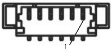
![Pure electrical connector pinout diagram without any text or symbols](.mcm-100-102-50-1z298-1000-10/84184db1530f45720d6693d5f245e225279fe11a8078c6318874ef65272f1e0a.jpg)

<table><tr><td>Pin</td><td>Signal</td></tr><tr><td>1</td><td>+3.3V</td></tr><tr><td>2</td><td>SOC_UART1_RX_CON</td></tr><tr><td>3</td><td>SOC_UART1_TX_CON</td></tr><tr><td>4</td><td>SOC_UART1_CTS_CON-L</td></tr><tr><td>5</td><td>SOC_UART1_RTS_CON-L</td></tr><tr><td>6</td><td>GND</td></tr></table>

Table B-2: HSUART Interface Wafer Pin Definitions

# B.2.2 USIM Port

Use of 3G/4G mini-PCIe module requires a SIM card for communication with telecom operator. The MCM-100/102 provides a USIM port connected to the mini-PCIe connector, with which a SIM card and 3G/4G mini-PCIe module can be installed to facilitate 3G/4G communication.

# B.2.3 Internal USB2.0 Interface Wafer

![Pure electrical connector pinout diagram without any text or symbols](.mcm-100-102-50-1z298-1000-10/a272151788dca0f9fdc96bc73ce754f3e52ca33b7c0e3da0c530598a09ce3ca9.jpg)

<table><tr><td>Pin</td><td>Signal</td></tr><tr><td>1</td><td>+5V</td></tr><tr><td>2</td><td>SOC_USB2_D6_P</td></tr><tr><td>3</td><td>SOC_USB2_D6_N</td></tr><tr><td>4</td><td>GND</td></tr><tr><td>5</td><td>+3.3V</td></tr><tr><td>6</td><td>USB2_WAFER-L</td></tr></table>

Table B-3: USB2.0 Interface Wafer Pin Definitions

# B.2.4 Internal I2C Interface Wafer

I2C and +3.3V/+5V power by this connector with cable. are provided by the connector with cable.

![Pure electrical connector diagram without any text or symbols](.mcm-100-102-50-1z298-1000-10/96ef76aa2c23b24bcc946b877e377a2e7d07472ae07b6e0144d0e57380873719.jpg)

<table><tr><td>Pin</td><td>Signal</td></tr><tr><td>1</td><td>GND</td></tr><tr><td>2</td><td>SOC_I2C1_CLK</td></tr><tr><td>3</td><td>SOC_I2C1_DAT</td></tr><tr><td>4</td><td>+3.3V</td></tr><tr><td>5</td><td>+5V</td></tr></table>

Table B-4: Internal I2C Interface Wafer Pin Definitions

# B.2.5 Clear CMOS Jumper

Under conditions in which the MCM-100/102 fails to boot, clearing the BIOS content stored in CMOS and restoring the default settings may be effective. To clear CMOS, short Pin 1 and Pin 2 of CN24 and remove the jumper, after which the CMOS will be restored to factory default settings.

![Simple diagram of a rectangular object with three square holes and a labeled arrow pointing to one corner (no text or symbols beyond the number 1)](.mcm-100-102-50-1z298-1000-10/ff2fd948c8ae5daacf6cd2613b1b87640a3bfd752cb2c2fc99557007c5794a00.jpg)

<table><tr><td>Pin</td><td>Signal</td></tr><tr><td>1</td><td>SOC_RTC_TEST-L</td></tr><tr><td>2</td><td>GND</td></tr><tr><td>3</td><td>SOC_RTC_RST-L-=p</td></tr></table>

Table B-5: Clear CMOS Jumper Pin Definition

# B.2.6 +5V GPS Antenna Power Header

External +5V power is reserved for GPS antenna power, with +5V provided by this connector with cable.

![Pure diagram of a rectangular device with internal components and labeled line (no text or symbols)](.mcm-100-102-50-1z298-1000-10/ee5a5e1a442f9c70954f0d73ff9a3020b1ed6f3f7ac88beee4a801ab2ac13f90.jpg)

<table><tr><td>Pin</td><td>Signal</td></tr><tr><td>1</td><td>+5</td></tr><tr><td>2</td><td>GND</td></tr></table>

Table B-6: +5V GPS Antenna Power Connector Pin Definition

# B.2.7 Internal SATA Interface Wafer

Reserved for extended 2.5” SSD, providing SATA signal and +3.3V/+5V power with cable.

![Technical diagram of an electronic component with pins and connectors (no text or symbols)](.mcm-100-102-50-1z298-1000-10/f9c44fcd348bcfd9fca686b94669ea1ba5e4db293e2e1f8deb866bd41ff1483c.jpg)

<table><tr><td>Pin</td><td>Signal</td><td>Pin</td><td>Signal</td></tr><tr><td>1</td><td>GND</td><td>13</td><td>+5V</td></tr><tr><td>2</td><td>SOC_SATA_TX1_P_C</td><td>14</td><td>+5V</td></tr><tr><td>3</td><td>SOC_SATA_TX1_N_C</td><td>15</td><td>+5V</td></tr></table>

Table B-7: SATA Wafer Pin Definition

<table><tr><td>Pin</td><td>Signal</td><td>Pin</td><td>Signal</td></tr><tr><td>4</td><td>GND</td><td>16</td><td>NC</td></tr><tr><td>5</td><td>SOC_SATA_RX1_N_C</td><td>17</td><td>GND</td></tr><tr><td>6</td><td>SOC_SATA_RX1_P_C</td><td>18</td><td>GND</td></tr><tr><td>7</td><td>GND</td><td>19</td><td>GND</td></tr><tr><td>8</td><td>NC</td><td>20</td><td>GND</td></tr><tr><td>9</td><td>+3.3V</td><td>G1</td><td>GND</td></tr><tr><td>10</td><td>+3.3V</td><td>G2</td><td>GND</td></tr><tr><td>11</td><td>+3.3V</td><td>G3</td><td>GND</td></tr><tr><td>12</td><td>NC</td><td>G4</td><td>GND</td></tr></table>

Table B-7: SATA Wafer Pin Definition

# B.2.8 Extended Power Wafer

Provides internal connectors for the power button.

![Simple diagram of a device casing with two slots and a labeled section (1), no text or symbols present.](.mcm-100-102-50-1z298-1000-10/0c5d484570fa5db46929fbb45692c249d103c9cfa39726c2c2e124e281c75199.jpg)

<table><tr><td>Pin</td><td>Signal</td></tr><tr><td>1</td><td>PWR_BTN_CN-L</td></tr><tr><td>2</td><td>GND</td></tr></table>

Table B-8: Extended Power Header Connector Pin Definition

# B.2.9 Internal I2C Interface Wafer

Provides the I2C signal and +3.3V power with cable.

![Pure electrical connector diagram without any text or symbols](.mcm-100-102-50-1z298-1000-10/9a71a4f236a240e2ed6f7f9c4af028b6ea0b08a317b53840d1508b07b9e70028.jpg)

<table><tr><td>Pin</td><td>Signal</td></tr><tr><td>1</td><td>+3.3V</td></tr><tr><td>2</td><td>SOC_I2C0_DAT</td></tr><tr><td>3</td><td>SOC_I2C0_CLK</td></tr><tr><td>4</td><td>SOC_I2C0_INT</td></tr><tr><td>5</td><td>GND</td></tr></table>

Table B-9: I2C Box Header Connector Pin Definition

# B.2.10 Extended Reset Wafer

Provides internal connectors for the reset button.

![Simple diagram of a rectangular device with two internal components and a labeled line pointing to one (no text or symbols beyond the number 1)](.mcm-100-102-50-1z298-1000-10/cdb748b3357514f5f1ef0863f7b436f2e837fc7f27c2a21e27f40fe1c42ad29e.jpg)

<table><tr><td>Pin</td><td>Signal</td></tr><tr><td>1</td><td>RESET_BTN_CN-L</td></tr><tr><td>2</td><td>GND</td></tr></table>

Table B-10: Extended Reset Header Connector Pin Definition

# B.2.11 RTC Battery Header

Links to the 3V coin battery pack for system RTC function.

![Simple diagram of a wall-mounted device with two slots and a labeled pin (no text or symbols beyond the number 1)](.mcm-100-102-50-1z298-1000-10/b9d85305b70f33bd0b2b35e0603f0c229f4500cd5ea9142b259c05e4981ca3a5.jpg)

<table><tr><td>Pin</td><td>Signal</td></tr><tr><td>1</td><td>P_+3V3_VBAT</td></tr><tr><td>2</td><td>GND</td></tr></table>

Table B-11: RTC Battery Connector Pin Definition

# B.2.12 Internal Speaker Wafer (Optional)

Provides the audio speaker signal, supporting 2x 2W8Ω speaker.

![Pure electrical connector diagram without any text or symbols](.mcm-100-102-50-1z298-1000-10/c0cc0c3ddbe9b5d928af4a4074decffb80165382c63f740712481b96af4526b3.jpg)

<table><tr><td>Pin</td><td>Signal</td></tr><tr><td>1</td><td>SPKR_L_P</td></tr><tr><td>2</td><td>SPKR_L_N</td></tr><tr><td>3</td><td>SPKR_R_P</td></tr><tr><td>4</td><td>SPKR_R_N</td></tr></table>

Table B-12: Speaker Wafer Pin Definition

# B.2.13 Internal MIC-IN & HP-OUT Wafer (Optional)

Provides MIC-IN and HP-OUT signals with cable.

![Pure electrical connector diagram without any text or symbols](.mcm-100-102-50-1z298-1000-10/f7116f049315f83ee7b4fd13b47f4b78ef8bf90623a4aa98d2ba9bb7c2a1173f.jpg)

<table><tr><td>Pin</td><td>Signal</td></tr><tr><td>1</td><td>EX_MIC_CN</td></tr><tr><td>2</td><td>HP_CN_L</td></tr><tr><td>3</td><td>HP_CN_R</td></tr><tr><td>4</td><td>AGND_AUDIO</td></tr></table>

Table B-13: MIC-IN & HP-OUT Wafer Pin Definition

# Important Safety Instructions

For user safety, please read and follow all instructions, Warnings, Cautions, and Notes marked in this manual and on the associated device before handling/operating the device, to avoid injury or damage.

S'il vous plaît prêter attention stricte à tous les avertissements et mises en garde figurant sur l'appareil , pour éviter des blessures ou des dommages.

 Read these safety instructions carefully
 Keep the User’s Manual for future reference
 Read the Specifications section of this manual for detailed information on the recommended operating environment
 The device can be operated at an ambient temperature of 50ºC
When installing/mounting or uninstalling/removing device; or when removal of a chassis cover is required for user servicing (See “Getting Started” on page 19.):

 Turn off power and unplug any power cords/cables
 Reinstall all chassis covers before restoring power

 To avoid electrical shock and/or damage to device:

 Keep device away from water or liquid sources
 Keep device away from high heat or humidity
 Keep device properly ventilated (do not block or cover ventilation openings)
 Always use recommended voltage and power source settings
 Always install and operate device near an easily accessible electrical outlet
 Secure the power cord (do not place any object on/over the power cord)
 Only install/attach and operate device on stable surfaces and/or recommended mountings

If the device will not be used for long periods of time, turn off and unplug from its power source

Never attempt to repair the device, which should only be serviced by qualified technical personnel using suitable tools
 A Lithium-type battery may be provided for uninterrupted backup or emergency power.

![The image features a yellow triangular warning sign with a black border. Inside the triangle is a black exclamation point. Below the triangle, the text 'CAUTION:' is printed in black capital letters.](.mcm-100-102-50-1z298-1000-10/06d35cfcad5737f04b74b430ae6ef1d6f625712006cbcc0572d9f8396852e842.jpg)

Risk of explosion if battery is replaced with one of an incorrect type; please dispose of used batteries appropriately.

Risque d’explosion si la pile est remplacée par une autre de type incorrect. Veuillez jeter les piles usagées de façon appropriée.

 The device must be serviced by authorized technicians when:

 The power cord or plug is damaged
 Liquid has entered the device interior
 The device has been exposed to high humidity and/or moisture
 The device is not functioning or does not function according to the User’s Manual
 The device has been dropped and/or damaged and/or shows obvious signs of breakage

Disconnect the power supply cord before loosening the thumbscrews and always fasten the thumbscrews with a screwdriver before starting the system up

 It is recommended that the device be installed only in a server room or computer room where access is:

 Restricted to qualified service personnel or users familiar with restrictions applied to the location, reasons therefor, and any precautions required

 Only afforded by the use of a tool or lock and key, or other means of security, and controlled by the authority responsible for the location

![Yellow triangular warning sign with black smoke symbol indicating hot weather](.mcm-100-102-50-1z298-1000-10/c9bc549268ade89ce19a25ea04ea5af58c5d018690ef507313c4c063aa4024bb.jpg)

# BURN HAZARD

Touching this surface could result in bodily injury. To reduce risk, allow the surface to cool before touching.

# RISQUE DE BRÛLURES

Ne touchez pas cette surface, cela pourrait entraîner des blessures.

Pour éviter tout danger, laissez la surface refroidir avant de la toucher.

This page intentionally left blank.

# Getting Service

Ask an Expert: http://askanexpert.adlinktech.com

# ADLINK Technology, Inc.

9F, No.166 Jian Yi Road, Zhonghe District

New Taipei City 235, Taiwan

Tel: +886-2-8226-5877

Fax: +886-2-8226-5717

Email: service@adlinktech.com

# Ampro ADLINK Technology, Inc.

5215 Hellyer Avenue, #110

San Jose, CA 95138, USA

Tel: +1-408-360-0200

Toll Free: +1-800-966-5200 (USA only)

Fax: +1-408-360-0222

Email: info@adlinktech.com

# ADLINK Technology (China) Co., Ltd.

300 Fang Chun Rd., Zhangjiang Hi-Tech Park

Pudong New Area, Shanghai, 201203 China

Tel: +86-21-5132-8988

Fax: +86-21-5132-3588

Email: market@adlinktech.com

# ADLINK Technology GmbH

Hans-Thoma-Strasse 11

D-68163 Mannheim, Germany

Tel: +49-621-43214-0

Fax: +49-621 43214-30

Email: emea@adlinktech.com

Please visit the Contact page at www.adlinktech.com for information on how to contact the ADLINK regional office nearest you:
[🔗 Link to the original document](.mcm-100-102-50-1z298-1000-10/mcm-100-102-50-1z298-1000-10.pdf)