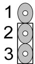
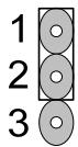
# miniBASE-10R User’s Manual

COM Express Type 10 Reference Carrier Board in Mini-ITX Form Factor
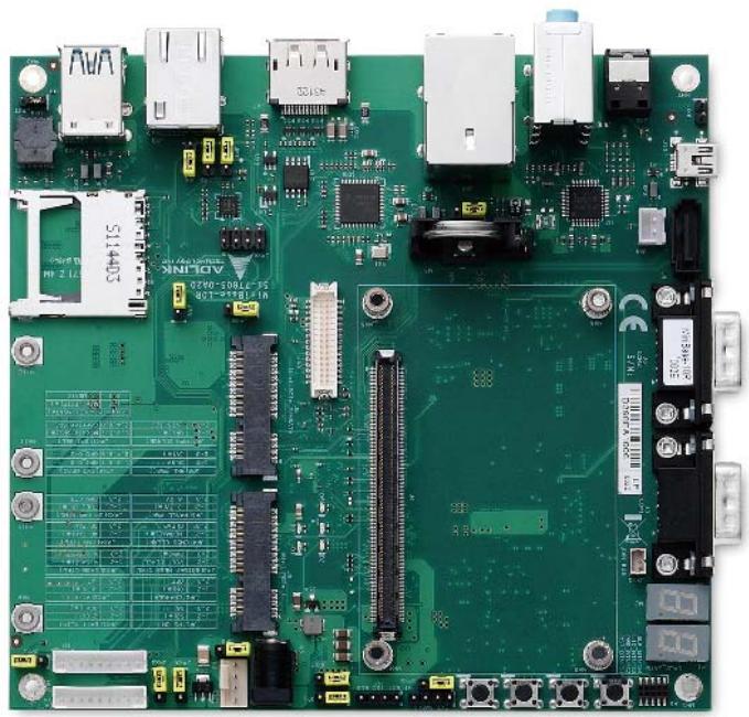
![Green printed circuit board with various electronic components and connectors (no readable text or symbols)](.minibase-10r-manual-en-20171110-v1/faeffc70e0221cdbd3d127dc83a9abfb553a91a73c61cb40cd8470f774e26a80.jpg)

![COM\nExpress®](.minibase-10r-manual-en-20171110-v1/e509cd567afbde12c49ab3da81774b84d7d9a6b7b0fafeb9da261936a1b241af.jpg)

Manual Rev.: 1.1

Revision Date: November 7, 2017

Part Number: 50-1V002-1010

# Preface

# Copyright

Copyright 2017 ADLINK Technology, Inc. This document contains proprietary information protected by copyright. All rights are reserved. No part of this manual may be reproduced by any mechanical, electronic, or other means in any form without prior written permission of the manufacturer.

# Disclaimer

The information in this document is subject to change without prior notice in order to improve reliability, design, and function and does not represent a commitment on the part of the manufacturer. In no event will the manufacturer be liable for direct, indirect, special, incidental, or consequential damages arising out of the use or inability to use the product or documentation, even if advised of the possibility of such damages.

# Environmental Responsibility

ADLINK is committed to fulfill its social responsibility to global environmental preservation through compliance with the European Union's Restriction of Hazardous Substances (RoHS) directive and Waste Electrical and Electronic Equipment (WEEE) directive. Environmental protection is a top priority for ADLINK. We have enforced measures to ensure that our products, manufacturing processes, components, and raw materials have as little impact on the environment as possible. When products are at their end of life, our customers are encouraged to dispose of them in accordance with the product disposal and/or recovery programs prescribed by their nation or company.

# Trademarks

Product names mentioned herein are used for identification purposes only and may be trademarks and/or registered trademarks of their respective companies.

Revision History

<table><tr><td>Revision</td><td>Description</td><td>Date</td><td>By</td></tr><tr><td>1.00</td><td>Initial release</td><td>2015-05-15</td><td>JC</td></tr><tr><td>1.1</td><td>Update functional block diagram, mechanical drawing, board layout, pinouts and LED info</td><td>2017-10-07</td><td>JC</td></tr></table>

# Table of Contents

Preface ............

List of Figures ....

List of Tables ... vi

1. Introduction...

2. Features...

2.1. Integrated Smart Battery Management System... .3
2.2. Secondary BIOS.. .3
2.3. Integrated Debug Port with Single Step Execution.. .3
2.4. Onboard Audio.. .3
2.5. Information LEDs.. .3
2.6. Power, Reset, Lid and Sleep Switches... 3

3. Component Locations......

4. Functional Diagram ....

5. Mechanical Drawing ........

6. Connectors, Pinouts and Jumpers .... .11

6.1. Carrier Board Signals – Type 10 .. .11
6.2. Connector and Pinout Compatibility . .12
6.3. Carrier Board Design. .. 12
6.4. COM Express Board-to-Board Connectors . .. 13
6.5. Display Connectors... .. 15
6.6. LVDS Jumper Settings . .17
6.7. Audio Connectors .. . 18
6.8. Mini PCIe and mSATA Connector .. .19
6.9. SATA .. . 22
6.10. USB and LAN .. .23
6.11. Serial Ports .... .24
6.12. I 2 C, SMBus and CAN Bus .. . 24
6.13. Fan Connector... . 25
6.14. Other Connectors . .26
6.15. Other Jumpers... .27
6.16. Power Connectors.. .28
6.17. Power Jumper Settings ....... .29

7. Secondary BIOS ...... .31

7.1. SPI Secondary BIOS . .31

# 8. Switches, POST and LEDs....... .33

8.1. Switches (S1-S4) .. .. 33
8.2. POST.. .. 33
8.3. Indicator LEDs .. .. 34

# 9. Smart Battery Management System ............. ..35

9.1. Input Power... .. 35
9.2. Charger Output Capability .. .. 35
9.3. Key Characteristics.. .. 35
9.4. Battery Settings .. .. 35
9.5. Windows OS Interface. .. 36

# Safety Instructions................. ..37

# Getting Service.............. ..38

# List of Figures

Figure 1: miniBASE-10R Component Locations . .5
Figure 2: miniBASE-10R Functional Block Diagram .
Figure 3: miniBASE-10R Mechanical Drawing.. 9
Figure 4: Carrier Board Signals - Type 10... . 11

# List of Tables

Table 1: miniBASE-10R AB Pin Definitions.... . 14

# 1. Introduction

The COM Express approach of custom carrier combined with off the shelf system cores is an excellent solution when you need to customize but lack the time or quantity for a complete redesign. It fits most system integration projects with production volumes from 500 to 10,000 pcs per year. The COM Express concept has a great many advantages over full custom designs, it reduces engineering complexity, lowers the threshold for total project quantity and last but not least brings your product to the market in no time. The average time to design a carrier board is less than half the time of a full custom OEM board.

The miniBASE-10R is a Mni-ITX size carrier board. Together with the COM Express Type 10 module of your choice and off-the-shelf add-on cards, you can quickly emulate the functionality of your desired end product for software development and hardware verification.

To build a functional prototype of your target system you will need:

COM Express Type 10 module
miniBASE-10R carrier board
PCI Express based or USB based add on cards
SATA drive storage or flash disk solution

The miniBASE-10R is compatible with Mini size Type 10 pinout COM Express modules and accommodates up to one Mini PCIe card, one Mini PCIe/mSATA card slot and one SD card.

The miniBASE-10R integrates a Smart Battery Management System that supports two Smart Batteries and 19V adapter input. The integrated Smart Battery Management System is compliant with the Smart Battery Manager Specification and uses the System Management Bus (SMBus) for communications between the battery power subsystem, Smart Batteries and host system (COM Express module). It is ACPI compliant and provides complete Smart Battery management under a supported operating system. ADLINK’s COM Express Type 10 modules feature a BIOS that fully supports all Smart Battery communications using existing interfaces defined in the COM Express specification and are fully compatible with the integrated Smart Battery Management System. The integrated Smart Battery Management System is a proof-of-concept battery power subsystem that allows for quick development and integration of battery power into a COM Express system in the following ways:

z To emulate the battery power subsystem functionality of your prototype system during the design phase
As a ready-made battery power subsystem for your customized system
z As a reference design to integrate a battery power subsystem into your custom-designed carrier

The miniBASE-10R is based on the PICMG COM Express (COM.0 Rev. 2.1) specification and follows the PICMG COM Express Carrier Design Guide (CDG) where possible (see 6.3 Carrier Board Designon page 12)

This page intentionally left blank.

# 2. Features

# 2.1. Integrated Smart Battery Management System

The miniBASE-10R integrates a Smart Battery Management System that support Dual Smart Batteries and 19V adapter. The Smart Battery Magagement System is a proof-of-concept battery power system that allows for quick development and integration of battery power into a COM Express system.

The Smart Battery Management System use the SM Bus for communications between battery power system, Smart Batteries and COM Express module. It is ACPI compliant and provides complete battery management under a supporting operating system.

Note: The selected COM Express module for miniBASE-10R must support wide voltage range input. (5.7V - 14V), even if Smart Battery power is not used.

# 2.2. Secondary BIOS

The miniBASE-10R supports the Serial Peripheral Interface (SPI) for COM Rev. 2.1 modules. Selection of active BIOS can be made by jumper settings. The jumper of the secondary BIOS is JPX7.

# 2.3. Integrated Debug Port with Single Step Execution

In addition to a two-digit POST code display, the board also provides a four-digit address display. By jumper selection the board can be switched into single step BIOS execution mode. Steps are executed using a manually operated onboard mini switch.

# 2.4. Onboard Audio

The miniBASE-10R has a Realtek ALC262 audio codec onboard. Audio I/O is provided by a three-jack connector.

# 2.5. Indicator LEDs

General information is obtained through indicator LEDs for power status, drive activity, and Mini PCIe card type (WWAN or WLAN). See 8.3 Indicator LEDs on page 34.

# 2.6. Power, Reset, Lid and Sleep Switches

The miniBASE-10R is equipped four mini switches (S1-4) for Reset, Power and COM.0 Rev.2.1 specified "Lid" and "Sleep" functions.

This page intentionally left blank.

# 3. Component Locations
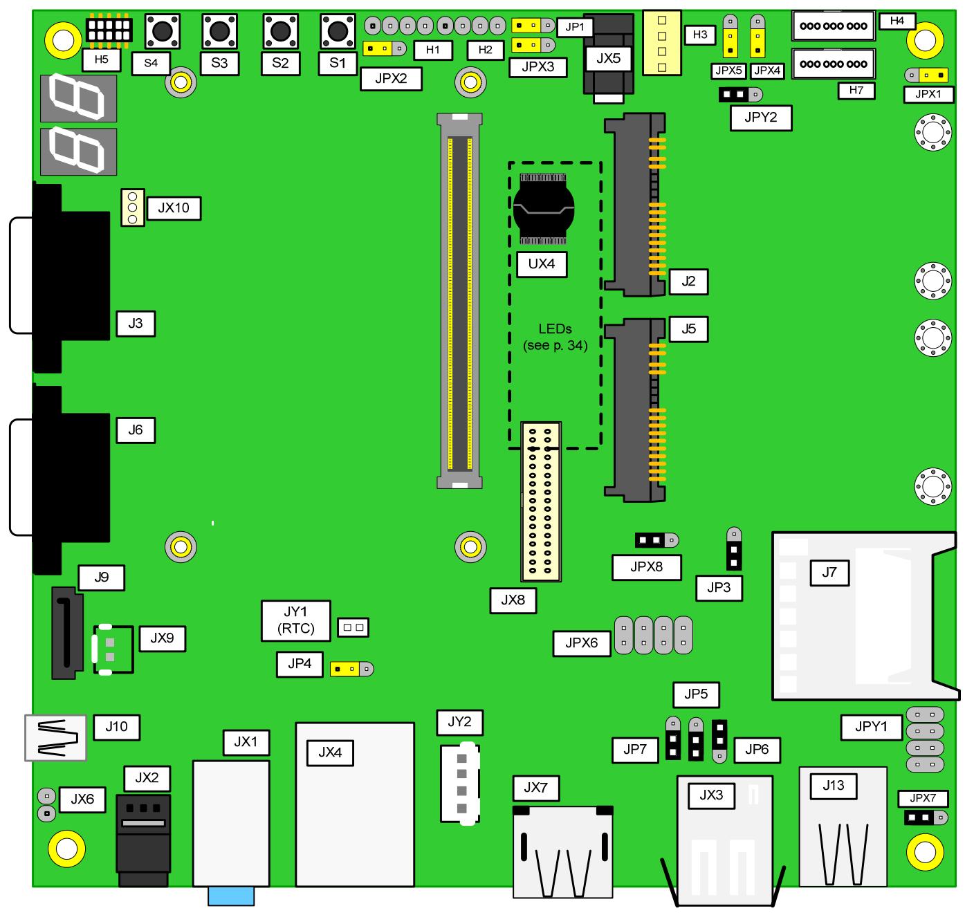
![H5 S4 S3 S2 S1 JPX2 H1 H2 JPX3 JX5 H3 JPX5 JPX4 000 000 000 H4\nJPY2\nJX10 UX4\nJ2\nJ5\nLEDs\n(see p. 34)\nJ9 JX8 JPX8 JP3 J7\nJX9 JY1 (RTC) JP4 JPX6 JP5\nJ10 JY2 JP7 JP6 JPY1\nJX6 JX2 JX1 JX4 JX7 JX3 J13 JPX7](.minibase-10r-manual-en-20171110-v1/7ce1fa2768eba2b65518dcb083e578257b11b5eb392037b9e5ffd975e6d1bd7a.jpg)

Figure 1: miniBASE-10R Component Locations
(See section 8.3 Indicator LEDs on page 34 for detailed LED locations.)

This page intentionally left blank.

# 4. Functional Diagram
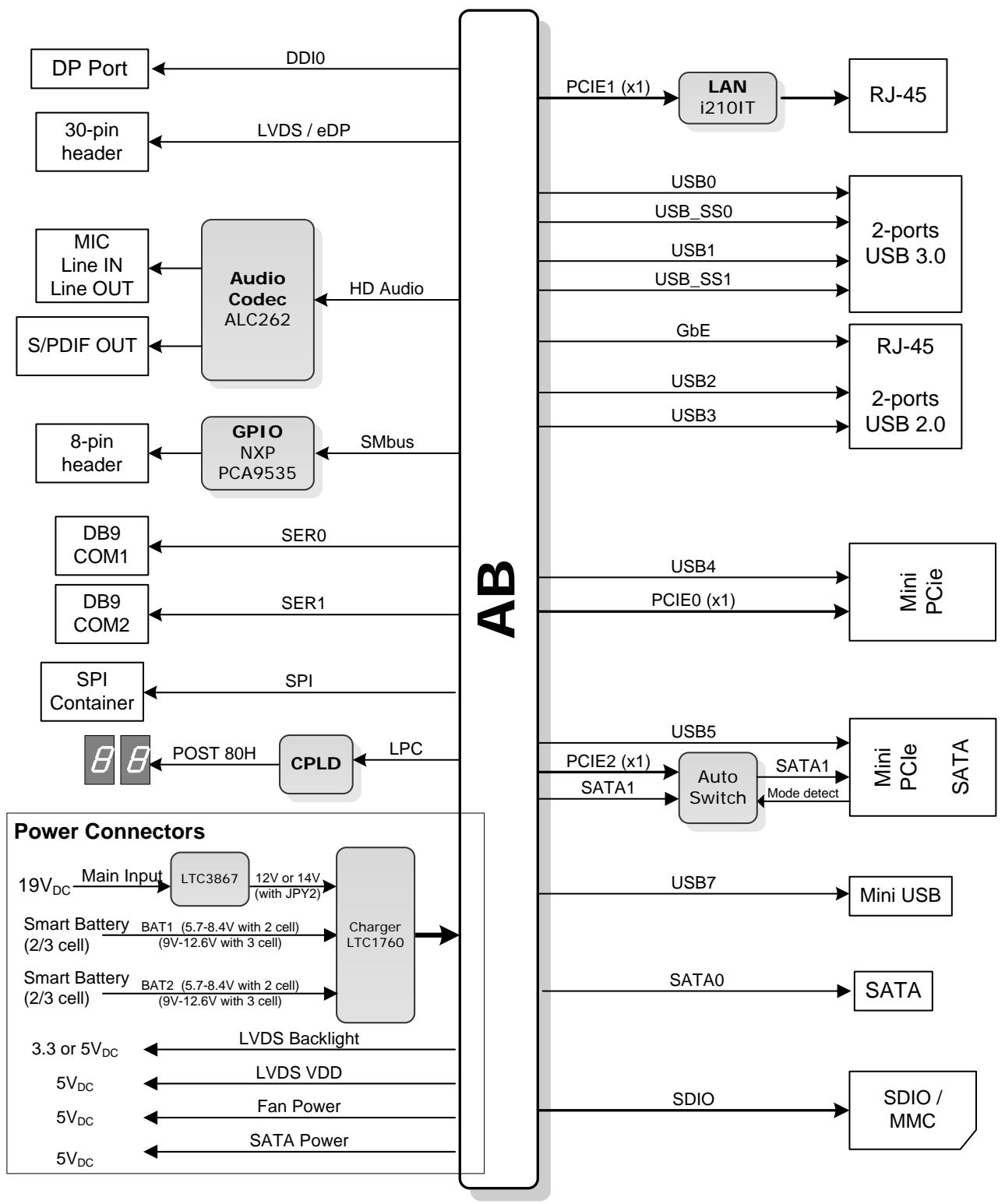
![The diagram illustrates a system block diagram centered around a vertical bus labeled **AB**. Connections flow between this central hub and various peripheral blocks on the left and right sides.\n\n**Left Side Connections:**\n*   **DP Port**: Connected via **DDI0**.\n*   **30-pin header**: Connected via **LVDS / eDP**.\n*   **Audio Codec ALC262**: Connected via **HD Audio**. It outputs to **MIC Line IN Line OUT** and **S/PDIF OUT**.\n*   **GPIO NXP PCA9535**: Connected via **Smbus**. It outputs to an **8-pin header**.\n*   **DB9 COM1**: Connected via **SER0**.\n*   **DB9 COM2**: Connected via **SER1**.\n*   **SPI Container**: Connected via **SPI**.\n*   **CPLD**: Connected via **LPC**. It outputs to a display block labeled **POST 80H**.\n*   **Power Connectors**: A section at the bottom left detailing power management:\n    *   **19VDC Main Input** connects to **LTC3867**.\n    *   **LTC3867** outputs **12V or 14V (with JPY2)** to **Charger LTC1760**.\n    *   **Smart Battery (2/3 cell) BAT1 (5.7-8.4V with 2 cell) (9V-12.6V with 3 cell)** connects to **Charger LTC1760**.\n    *   **Smart Battery (2/3 cell) BAT2 (5.7-8.4V with 2 cell) (9V-12.6V with 3 cell)** connects to **Charger LTC1760**.\n    *   **Charger LTC1760** connects to **AB**.\n    *   **AB** provides power to the connectors: **LVDS Backlight** (**3.3 or 5VDC**), **LVDS VDD** (**5VDC**), **Fan Power** (**5VDC**), and **SATA Power** (**5VDC**).\n\n**Right Side Connections:**\n*   **LAN i210IT**: Connected via **PCIE1 (x1)**. It connects to **RJ-45**.\n*   **2-ports USB 3.0**: Connected via **USB0**, **USB_SS0**, **USB1**, and **USB_SS1**.\n*   **RJ-45**: Connected via **GbE**.\n*   **2-ports USB 2.0**: Connected via **USB2** and **USB3**.\n*   **Mini PCIe**: Connected via **USB4** and **PCIE0 (x1)**.\n*   **Mini PCIe SATA**: Connected via **USB5** and an **Auto Switch**. The **Auto Switch** receives inputs **PCIE2 (x1)** and **SATA1** from AB and outputs a signal labeled **Mode detect** to the **Mini PCIe SATA** block.\n*   **Mini USB**: Connected via **USB7**.\n*   **SATA**: Connected via **SATA0**.\n*   **SDIO / MMC**: Connected via **SDIO**.](.minibase-10r-manual-en-20171110-v1/e77466207675a75cbd6488fff4ed0c1ca25f2f5ad29cd12f75c79415f48a8162.jpg)

Figure 2: miniBASE-10R Functional Block Diagram

This page intentionally left blank.

# 5. Mechanical Drawing
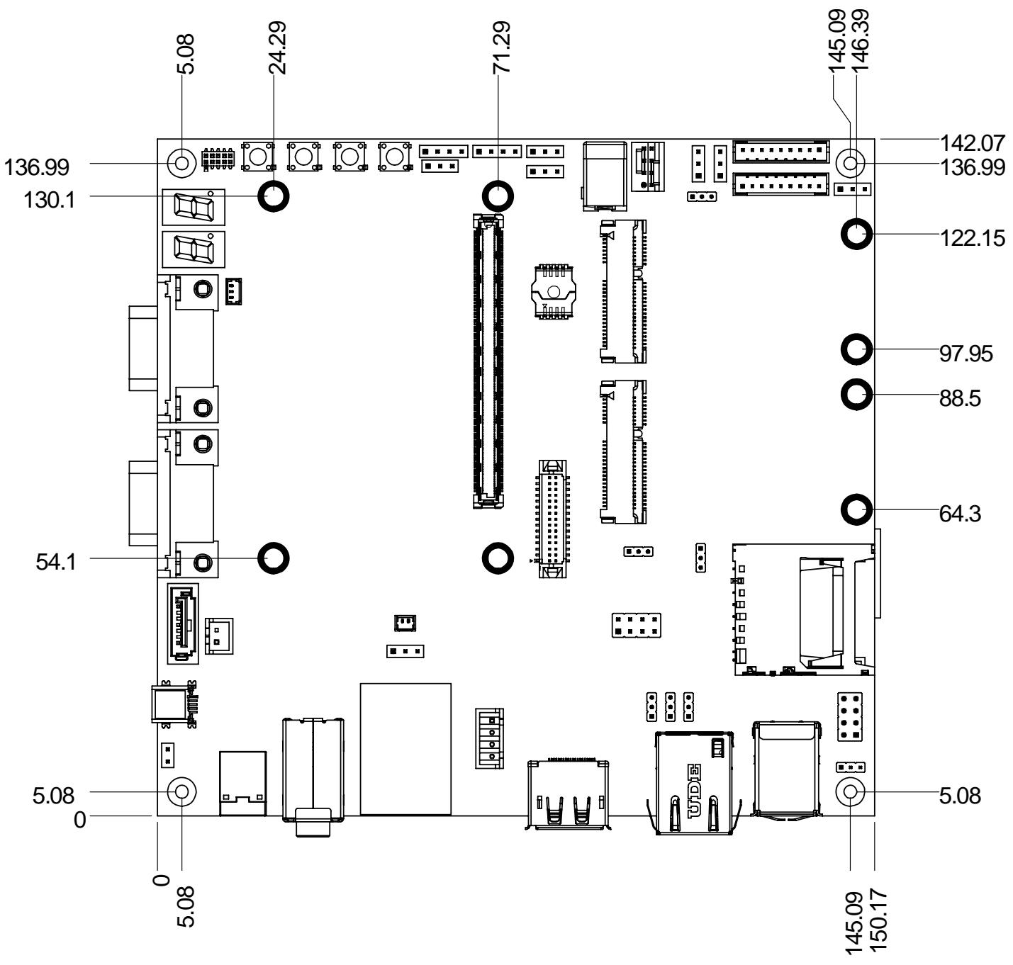
![The image displays a technical line drawing of a motherboard layout with dimension lines and numerical values indicating measurements. The text visible in the image consists of the following numbers and a label:\n\n**Top and Left Area:**\n*   5.08\n*   24.29\n*   136.99\n*   130.1\n\n**Top Center and Right Area:**\n*   71.29\n*   145.09\n*   146.39\n*   142.07\n*   136.99\n\n**Right Side (Mounting Holes):**\n*   122.15\n*   97.95\n*   88.5\n*   64.3\n\n**Left Side (Mounting Holes):**\n*   54.1\n*   5.08\n\n**Bottom Area:**\n*   0\n*   5.08\n*   145.09\n*   150.17\n\n**On the Board:**\n*   UD11](.minibase-10r-manual-en-20171110-v1/5694c4d122e76b01652875d6bfcd43660b8479b28e429128e0badee4b3f843c2.jpg)
All dimensions are shown in millimeters.
Tolerances should be ± 0.25mm, unless otherwise noted.The tolerances on the PCB corner locating peg holes (dimensions [5.08, 5.08], [145.09, 5.08], [5.08, 136.99] and [145.09, 136.99]) should be ± 0.10mm.

Figure 3: miniBASE-10R Mechanical Drawing

This page intentionally left blank.

# 6. Connectors, Pinouts and Jumpers

# 6.1. Carrier Board Signals – Type 10
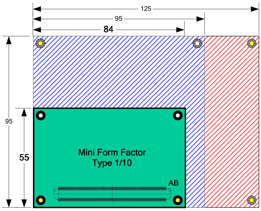
![| Section | Dimension |\n| ------- | --------- |\n| Top Left | 125       |\n| Top Right | 84        |\n| Bottom Left | 55      |\n| Bottom Right | 95      |](.minibase-10r-manual-en-20171110-v1/2a0d5de36d05b0adde14efd4603f87cf0f0a4a79d08398aa7de0123377bc0bfa.jpg)

Dimensions in mm

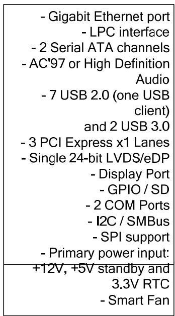
![- Gigabit Ethernet port\n- LPC interface\n- 2 Serial ATA channels\n- AC'97 or High Definition\nAudio\n- 7 USB 2.0 (one USB\nclient)\nand 2 USB 3.0\n- 3 PCI Express x1 Lanes\n- Single 24-bit LVDS/eDP\n- Display Port\n- GPIO / SD\n- 2 COM Ports\n- I2C / SMBus\n- SPI support\n- Primary power input:\n+12V, +5V standby and\n3.3V RTC\n- Smart Fan](.minibase-10r-manual-en-20171110-v1/28a16eb22fda0fd631db3ff4866132372c8e0bd5ad9105571d3d00d8d58c18d4.jpg)

AB Connector
Figure 4: Carrier Board Signals - Type 10

# 6.2. Connector and Pinout Compatibility

Connectors positions and pinouts comply with pinout and signal descriptions in the “PICMG® COM.0 - COM Express Module Base specification, Revision 2”. This document includes: description of pinouts, signal descriptions and mechanical characteristics of the COM Express specification. The miniBASE-10R is compatible with COM Express modules in mini size form factor, Type 10 pinout, COM.0 Rev. 2.1.

# 6.3. Carrier Board Design

The miniBASE-10R follows the PICMG COM Express Carrier Design Guide (CDG) where possible. The miniBASE-10R design and schematics are fully verified, and we recommend that you follow them as a reference for your carrier board design. miniBASE-10R Schematics and Mechanical files as well as the CDG can be downloaded from the miniBASE-10R product webpage: http://www.adlinktech.com/PD/web/PD\_detail.php?cKind=&pid=1362

![COM Express®\nCarrier Design Guide\n\nCOM Express®\nCarrier Design Guide\n\nGuidelines for designing COM Express® Carrier Boards\n\nDecember 6, 2013\n\nRev. 2.0\n\nThis design goes to a specification. It contains additional detail information but does not replace the COM Express® Carrier Boards specification.\n\nFor complete guidelines on the design of COM Express® carrier boards and samples, we also provide for specification - do not use this design guide as the only reference for any design decision. This design goes to a specific composition with COM Express®.](.minibase-10r-manual-en-20171110-v1/63b2d82076b6888ebad39595ab3e55a1178cec92d4ff87a4685597d3ccab237a.jpg)

# 6.4. COM Express Board-to-Board Connectors

Signals and Pinout comply with COM Express Type 10

![B1\nA1\nB110\nA B\nA110](.minibase-10r-manual-en-20171110-v1/26b421ff1ffb33e4f48801bdbe47709c316c060cad67849088cece54a14c6667.jpg)

COM.0 Type 10 rev. 2.1

<table><tr><td>Pin</td><td>Row A</td><td>Row B</td></tr><tr><td>1</td><td>GND(FIXED)</td><td>GND(FIXED)</td></tr><tr><td>2</td><td>GBE0_MDI3-</td><td>GBE0_ACT#</td></tr><tr><td>3</td><td>GBE0_MDI3+</td><td>LPC_FRAME#</td></tr><tr><td>4</td><td>GBE0_LINK100#</td><td>LPC_AD0</td></tr><tr><td>5</td><td>GBE0_LINK1000#</td><td>LPC_AD1</td></tr><tr><td>6</td><td>GBE0_MDI2-</td><td>LPC_AD2</td></tr><tr><td>7</td><td>GBE0_MDI2+</td><td>LPC_AD3</td></tr><tr><td>8</td><td>GBE0_LINK#</td><td>LPC_DRQ0#</td></tr><tr><td>9</td><td>GBE0_MDI1-</td><td>LPC_DRQ1#</td></tr><tr><td>10</td><td>GBE0_MDI1+</td><td>LPC_CLK</td></tr><tr><td>11</td><td>GND(FIXED)</td><td>GND(FIXED)</td></tr><tr><td>12</td><td>GBE0_MDI0-</td><td>PWRBTN#</td></tr><tr><td>13</td><td>GBE0_MDI0+</td><td>SMB_CK</td></tr><tr><td>14</td><td>GBE0_CTREF</td><td>SMB_DAT</td></tr><tr><td>15</td><td>SUS_S3#</td><td>SMB_ALERT#</td></tr><tr><td>16</td><td>SATA0_TX+</td><td>SATA1_TX+</td></tr><tr><td>17</td><td>SATA0_TX-</td><td>SATA1_TX-</td></tr><tr><td>18</td><td>SUS_S4#</td><td>SUS_STAT#</td></tr><tr><td>19</td><td>SATA0_RX+</td><td>SATA1_RX+</td></tr><tr><td>20</td><td>SATA0_RX-</td><td>SATA1_RX-</td></tr><tr><td>21</td><td>GND(FIXED)</td><td>GND(FIXED)</td></tr><tr><td>22</td><td>USB_SSRX0-</td><td>USB_SSTX0-</td></tr><tr><td>23</td><td>USB_SSRX0+</td><td>USB_SSTX0+</td></tr><tr><td>24</td><td>SUS_S5#</td><td>PWR_OK</td></tr><tr><td>25</td><td>USB_SSRX1-</td><td>USB_SSTX1-</td></tr><tr><td>26</td><td>USB_SSRX1+</td><td>USB_SSTX1+</td></tr><tr><td>27</td><td>BATLOW#</td><td>WDT</td></tr><tr><td>28</td><td>(S)ATA_ACT#</td><td>AC/HDA_SDIN2</td></tr><tr><td>29</td><td>AC/HDA_SYNC</td><td>AC/HDA_SDIN1</td></tr><tr><td>30</td><td>AC/HDA_RST#</td><td>AC/HDA_SDIN0</td></tr><tr><td>31</td><td>GND(FIXED)</td><td>GND(FIXED)</td></tr><tr><td>32</td><td>AC/HDA_BITCLK</td><td>SPKR</td></tr><tr><td>33</td><td>AC/HDA_SDOUT</td><td>I2C_CK</td></tr><tr><td>34</td><td>BIOS_DIS0#</td><td>I2C_DAT</td></tr><tr><td>35</td><td>THRMTRIP#</td><td>THRM#</td></tr><tr><td>36</td><td>USB6-</td><td>USB7-</td></tr><tr><td>37</td><td>USB6+</td><td>USB7+</td></tr><tr><td>38</td><td>USB_6_7_OC#</td><td>USB_4_5_OC#</td></tr><tr><td>39</td><td>USB4-</td><td>USB5-</td></tr><tr><td>40</td><td>USB4+</td><td>USB5+</td></tr><tr><td>41</td><td>GND(FIXED)</td><td>GND(FIXED)</td></tr><tr><td>42</td><td>USB2-</td><td>USB3-</td></tr><tr><td>43</td><td>USB2+</td><td>USB3+</td></tr><tr><td>44</td><td>USB_2_3_OC#</td><td>USB_0_1_OC#</td></tr><tr><td>45</td><td>USB0-</td><td>USB1-</td></tr><tr><td>46</td><td>USB0+</td><td>USB1+</td></tr><tr><td>47</td><td>VCC_RTC</td><td>EXCD1_PERST#</td></tr><tr><td>48</td><td>EXCD0_PERST#</td><td>EXCD1_CPPE#</td></tr><tr><td>49</td><td>EXCD0_CPPE#</td><td>SYS_RESET#</td></tr><tr><td>50</td><td>LPC_SERIRQ</td><td>CB_RESET#</td></tr><tr><td>51</td><td>GND(FIXED)</td><td>GND(FIXED)</td></tr></table>

COM.0 Type 10 rev. 2.1

<table><tr><td>Pin</td><td>Row A</td><td>Row B</td></tr><tr><td>52</td><td>RSVD</td><td>RSVD</td></tr><tr><td>53</td><td>RSVD</td><td>RSVD</td></tr><tr><td>54</td><td>GPIO</td><td>GPO1</td></tr><tr><td>55</td><td>RSVD</td><td>RSVD</td></tr><tr><td>56</td><td>RSVD</td><td>RSVD</td></tr><tr><td>57</td><td>GND</td><td>GPO2</td></tr><tr><td>58</td><td>PCIE_TX3+</td><td>PCIE_RX3+</td></tr><tr><td>59</td><td>PCIE_TX3-</td><td>PCIE_RX3-</td></tr><tr><td>60</td><td>GND(FIXED)</td><td>GND(FIXED)</td></tr><tr><td>61</td><td>PCIE_TX2+</td><td>PCIE_RX2+</td></tr><tr><td>62</td><td>PCIE_TX2-</td><td>PCIE_RX2-</td></tr><tr><td>63</td><td>GPI1</td><td>GPO3</td></tr><tr><td>64</td><td>PCIE_TX1+</td><td>PCIE_RX1+</td></tr><tr><td>65</td><td>PCIE_TX1-</td><td>PCIE_RX1-</td></tr><tr><td>66</td><td>GND</td><td>WAKE0#</td></tr><tr><td>67</td><td>GPI2</td><td>WAKE1#</td></tr><tr><td>68</td><td>PCIE_TX0+</td><td>PCIE_RX0+</td></tr><tr><td>69</td><td>PCIE_TX0-</td><td>PCIE_RX0-</td></tr><tr><td>70</td><td>GND(FIXED)</td><td>GND(FIXED)</td></tr><tr><td>71</td><td>LVDS_A0+/ eDP_TX2+</td><td>DDI0_PAIR0+</td></tr><tr><td>72</td><td>LVDS_A0-/ eDP_TX2-</td><td>DDI0_PAIR0-</td></tr><tr><td>73</td><td>LVDS_A1+/ eDP_TX1+</td><td>DDI0_PAIR1+</td></tr><tr><td>74</td><td>LVDS_A1-/ eDP_TX1-</td><td>DDI0_PAIR1-</td></tr><tr><td>75</td><td>LVDS_A2+/ eDP_TX0+</td><td>DDI0_PAIR2+</td></tr><tr><td>76</td><td>LVDS_A2-/ eDP_TX0-</td><td>DDI0_PAIR2-</td></tr><tr><td>77</td><td>LVDS_/eDP_VDD_EN</td><td>DDI0_PAIR4+</td></tr><tr><td>78</td><td>LVDS_A3+</td><td>DDI0_PAIR4-</td></tr><tr><td>79</td><td>LVDS_A3-</td><td>LVDS_/eDP_BKLT_EN</td></tr><tr><td>80</td><td>GND(FIXED)</td><td>GND(FIXED)</td></tr><tr><td>81</td><td>LVDS_A_CK+/ eDP_TX3+</td><td>DDI0_PAIR3+</td></tr><tr><td>82</td><td>LVDS_A_CK-/ eDP_TX3-</td><td>DDI0_PAIR3-</td></tr><tr><td>83</td><td>LVDS_I2C_CK/ eDP_AUX+</td><td>LVDS_/eDP_BKLT_CTRL</td></tr><tr><td>84</td><td>LVDS_I2C_DAT/ eDP_AUX-</td><td>VCC_5V_SBY</td></tr><tr><td>85</td><td>GPI3</td><td>VCC_5V_SBY</td></tr><tr><td>86</td><td>RSVD</td><td>VCC_5V_SBY</td></tr><tr><td>87</td><td>eDP_HPD</td><td>VCC_5V_SBY</td></tr><tr><td>88</td><td>PCIE_CLK_REF+</td><td>BIOS_DIS1#</td></tr><tr><td>89</td><td>PCIE_CLK_REF-</td><td>DDO_HPD</td></tr><tr><td>90</td><td>GND(FIXED)</td><td>GND(FIXED)</td></tr><tr><td>91</td><td>SPI_POWER</td><td>DDI0_PAIR5+</td></tr><tr><td>92</td><td>SPI_MISO</td><td>DDI0_PAIR5-</td></tr><tr><td>93</td><td>GPO0</td><td>DDI0_PAIR6+</td></tr><tr><td>94</td><td>SPI_CLK</td><td>DDI0_PAIR6-</td></tr><tr><td>95</td><td>SPI_MOSI</td><td>DDI0_DDC_AUX_SEL</td></tr><tr><td>96</td><td>TPM_PP</td><td>USB_HOST_PRSNT</td></tr><tr><td>97</td><td>TYPE10#</td><td>SPI_CS#</td></tr><tr><td>98</td><td>SER0_TX</td><td>DDI0_CTRLCLK_AUX+</td></tr><tr><td>99</td><td>SER0_RX</td><td>DDI0_CTRLDATA_AUX-</td></tr><tr><td>100</td><td>GND(FIXED)</td><td>GND(FIXED)</td></tr><tr><td>101</td><td>SER1_TX / CAN_TX</td><td>FAN_PWMOUT</td></tr><tr><td>102</td><td>SER1_RX / CAN_RX</td><td>FAN_TACHIN</td></tr><tr><td>103</td><td>LID#</td><td>SLEEP#</td></tr><tr><td>104</td><td>VCC_12V</td><td>VCC_12V</td></tr><tr><td>105</td><td>VCC_12V</td><td>VCC_12V</td></tr><tr><td>106</td><td>VCC_12V</td><td>VCC_12V</td></tr><tr><td>107</td><td>VCC_12V</td><td>VCC_12V</td></tr><tr><td>108</td><td>VCC_12V</td><td>VCC_12V</td></tr><tr><td>109</td><td>VCC_12V</td><td>VCC_12V</td></tr><tr><td>110</td><td>GND(FIXED)</td><td>GND(FIXED)</td></tr></table>

Table 1: miniBASE-10R AB Pin Definitions

# 6.5. Display Connectors

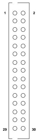
# 6.5.1. JX8: LVDS/eDP Connector

For LVDS panel
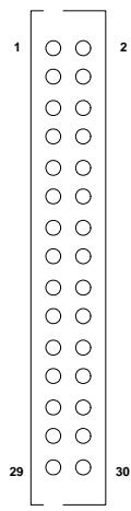
![1\n2\n29\n30](.minibase-10r-manual-en-20171110-v1/2c06cdb17f96a0d480bd06a004d9b454cdaf9d7f87cd00c369f15c5cddc43670.jpg)

<table><tr><td>Pin</td><td>Signal</td><td>Pin</td><td>Signal</td></tr><tr><td>1</td><td>LVDS_A0+</td><td>2</td><td>Panel_PWR</td></tr><tr><td>3</td><td>LVDS_A0-</td><td>4</td><td>Panel_PWR</td></tr><tr><td>5</td><td>GND</td><td>6</td><td>Panel_EDID_PWR</td></tr><tr><td>7</td><td>LVDS_A1+</td><td>8</td><td>BKLT_PWR</td></tr><tr><td>9</td><td>LVDS_A1-</td><td>10</td><td>BKLT_PWR</td></tr><tr><td>11</td><td>GND</td><td>12</td><td>GND</td></tr><tr><td>13</td><td>LVDS_A2+</td><td>14</td><td>BKLT_CTRL</td></tr><tr><td>15</td><td>LVDS_A2-</td><td>16</td><td>BKLT_EN</td></tr><tr><td>17</td><td>GND</td><td>18</td><td>GND</td></tr><tr><td>19</td><td>LVDS_A3+</td><td>20</td><td>N.C</td></tr><tr><td>21</td><td>LVDS_A3-</td><td>22</td><td>LVDS_VDD_EN</td></tr><tr><td>23</td><td>GND</td><td>24</td><td>N.C</td></tr><tr><td>25</td><td>LVDS_A_CLK+</td><td>26</td><td>LVDS_I2C_DATA</td></tr><tr><td>27</td><td>LVDS_A_CLK-</td><td>28</td><td>LVDS_I2C_CLK</td></tr><tr><td>29</td><td>GND</td><td>30</td><td>GND</td></tr></table>

For eDP panel
![1\n2\n29\n30](.minibase-10r-manual-en-20171110-v1/c8d050d399936af237278b9408e7087a8dde5c6c48c5235777e5a5465dc60473.jpg)

<table><tr><td>Pin</td><td>Signal</td><td>Pin</td><td>Signal</td></tr><tr><td>1</td><td>eDP_TX2+</td><td>2</td><td>Panel_PWR</td></tr><tr><td>3</td><td>eDP_TX2-</td><td>4</td><td>Panel_PWR</td></tr><tr><td>5</td><td>GND</td><td>6</td><td>N.C</td></tr><tr><td>7</td><td>eDP_TX1+</td><td>8</td><td>N.C</td></tr><tr><td>9</td><td>eDP_TX1-</td><td>10</td><td>N.C</td></tr><tr><td>11</td><td>GND</td><td>12</td><td>N.C</td></tr><tr><td>13</td><td>eDP_TX0+</td><td>14</td><td>BKLT_CTRL</td></tr><tr><td>15</td><td>eDP_TX0-</td><td>16</td><td>BKLT_EN</td></tr><tr><td>17</td><td>GND</td><td>18</td><td>GND</td></tr><tr><td>19</td><td>N.C</td><td>20</td><td>N.C</td></tr><tr><td>21</td><td>N.C</td><td>22</td><td>N.C</td></tr><tr><td>23</td><td>GND</td><td>24</td><td>Hot_Plug</td></tr><tr><td>25</td><td>eDP_TX3+</td><td>26</td><td>eDP_AUX-</td></tr><tr><td>27</td><td>eDP_TX3-</td><td>28</td><td>eDP_AUX+</td></tr><tr><td>29</td><td>GND</td><td>30</td><td>GND</td></tr></table>

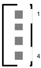
# 6.5.2. JY2: eDP Backlight Voltage

![The image displays a schematic diagram featuring a vertical column of four grey squares. To the left of the squares is a thick black bracket shape. To the right of the squares is a vertical axis line with small horizontal tick marks. Next to this axis, the number '1' is positioned at the top level, aligned with the top square, and the number '4' is positioned at the bottom level, aligned with the bottom square.](.minibase-10r-manual-en-20171110-v1/26f00f5eff975ae4222d1eb43b072a9e2efcd1e700906e9d3327da7be5dc7271.jpg)

<table><tr><td>Connector</td><td>Status</td></tr><tr><td>1-2</td><td>GND</td></tr><tr><td>2-3</td><td>5-14V</td></tr></table>

# 6.5.3. JX7: DisplayPort

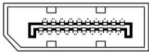
(From DDI0 signal on AB connector)
![The image is a schematic line drawing of an electronic connector. It features a rectangular outline with a slanted or chamfered corner on the bottom left. Inside the outline, there are four small rectangular cutouts positioned near the top and bottom edges, likely serving as mounting holes. Centered within the connector is a thick, black, U-shaped trace or track. Along the top horizontal segment of this U-shape, there is a row of 20 small circles arranged side-by-side, representing contact points or pins.](.minibase-10r-manual-en-20171110-v1/cc23c22e4bebfb94aba5f36cac867b43c818967a4ef68fb4c96eca00df88e01a.jpg)

<table><tr><td>Pin</td><td>Signal</td><td>Pin</td><td>Signal</td></tr><tr><td>1</td><td>Lane0_P</td><td>2</td><td>GND</td></tr><tr><td>3</td><td>Lane0_N</td><td>4</td><td>Lane1_P</td></tr><tr><td>5</td><td>GND</td><td>6</td><td>Lane1_N</td></tr><tr><td>7</td><td>Lane2_P</td><td>8</td><td>GND</td></tr><tr><td>9</td><td>Lane2_N</td><td>10</td><td>Lane3_P</td></tr><tr><td>11</td><td>GND</td><td>12</td><td>Lane3_N</td></tr><tr><td>13</td><td>CONFIG1 *</td><td>14</td><td>CONFIG2 *</td></tr><tr><td>15</td><td>AUX_P</td><td>16</td><td>GND</td></tr><tr><td>17</td><td>AUX_N</td><td>18</td><td>Hot_Plug</td></tr><tr><td>19</td><td>RTN_PWR</td><td>20</td><td>PWR</td></tr></table>

# 6.6. LVDS Jumper Settings

# 6.6.1. JP5: Panel Power Voltage

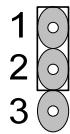
Selects the LVDS Panel Power voltage on JX8
![The image features a vertical arrangement. On the left side, the numbers '1', '2', and '3' are stacked from top to bottom in bold black font. To the right of each number is a grey circle with a white center, aligned in a column.](.minibase-10r-manual-en-20171110-v1/2f5f043293ba59af69217b94afe1991f2fbacfd1cace8892054af07fed5d088e.jpg)

<table><tr><td>Jumper</td><td colspan="2">Status</td></tr><tr><td>1-2</td><td>+ 3.3V</td><td>&lt;&lt;&lt;&lt;</td></tr><tr><td>2-3</td><td>+ 5.0V</td><td></td></tr></table>

# 6.6.2. JP6: Backlight Power Voltage

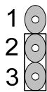
Selects the Backlight Panel Power voltage on JX8
![The image displays a vertical list of the numbers 1, 2, and 3 in bold black font on the left. To the right of each number is a column of grey circles stacked vertically, corresponding to the number's value: one circle next to 1, two stacked circles next to 2, and three stacked circles next to 3. The circles have a lighter grey center surrounded by a darker grey ring.](.minibase-10r-manual-en-20171110-v1/57d65be32852f2f34384033b5a866da4275a3dbf08f038ec1e0671404562aeef.jpg)

<table><tr><td>Jumper</td><td colspan="2">Status</td></tr><tr><td>1-2</td><td>+ 3.3V</td><td></td></tr><tr><td>2-3</td><td>+ 5.0V</td><td>&lt;&lt;&lt;&lt;</td></tr></table>

# 6.6.3. JP3: Brightness Control

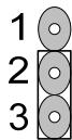
Sets the Panel Brightness Control to Voltage Level Or PWM. When set to Voltage Level, the Backlight CTRL signal can be varied from 0-5V in 0.5V increments
![The image displays a vertical list featuring the numbers 1, 2, and 3 in bold black font on the left side. To the right of each number is a corresponding light grey circle with a darker grey center, resembling a coin or token. The circles are stacked vertically in alignment with the numbers.](.minibase-10r-manual-en-20171110-v1/7ffd19d27dac08e30e57cd8665f6a0f241ee9d888f1ea1ffc789ec34a3a7a5f4.jpg)

<table><tr><td>Jumper</td><td>Status</td></tr><tr><td>1-2</td><td>Voltage Level</td></tr><tr><td>2-3</td><td>PWM &lt;&lt;&lt;</td></tr></table>

# 6.6.4. JP7: Brightness PWM Source

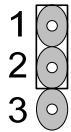
Sets the Panel Brightness PWM Source to GPU or LVDS I2C. When Brightness PWM Source is set to LVDS I2C, the user will be able to use the SEMA command to control the PWM pulse to the panel backlight
![The image displays the numbers **1**, **2**, and **3** stacked vertically on the left side. To their right are three vertical columns of circles. Each column consists of three grey circles with white concentric rings stacked vertically. The layout creates three horizontal rows, where each row begins with a number followed by three circles.](.minibase-10r-manual-en-20171110-v1/9c8c99c6d5e84998bf342e9d96261ec4c094f686df7432e1f48a17e9035fe369.jpg)

<table><tr><td>Jumper</td><td>Status</td></tr><tr><td>1-2</td><td>GPU &lt;&lt;&lt;</td></tr><tr><td>2-3</td><td>LVDS I2C</td></tr></table>

Note: &lt;&lt;&lt;&lt; indicates default setting

# 6.7. Audio Connectors

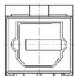
# 6.7.1. JX2: S/PDIF Output Jack (optical)
![The image displays a technical floor plan with numerical dimensions annotated in white text. Along the top edge, the numbers read from left to right: '208 208 208 208 208 208'. On the left vertical edge, the numbers are '396 396'. Along the bottom edge, the numbers read from left to right: '120 240 240 240 240 240'. The central drawing outlines a room layout with internal partitions and a central rectangular shape.](.minibase-10r-manual-en-20171110-v1/bf84bd4f7e95712484d686869d4320583375b04d929a7e0526f2bf0856eaa18f.jpg)

# 6.7.2. JX6: S/PDIF Output Header

![A graphic of a rounded rectangle containing two small squares, resembling a power switch, positioned next to the number 1.](.minibase-10r-manual-en-20171110-v1/6b2a5bb3c7f92e1adb5b39b0ca548af7528722c8ba7baf118a794ab5bafa5955.jpg)

&lt;table&gt;<tr><td>Pin</td><td>Signal</td><td>Pin</td><td>Signal</td></tr><tr><td>1</td><td>SPDIF - Out</td><td>2</td><td>GND</td></tr></table>

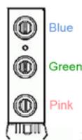
# 6.7.3. JX1: Three-in-One Audio Phone Jack
![The image displays a vertical column of three circular audio jacks. To the right of the top jack is the word 'Blue' in blue text. To the right of the middle jack is the word 'Green' in green text. To the right of the bottom jack is the word 'Pink' in pink text. Below the bottom jack is a rectangular connector base with small vertical lines.](.minibase-10r-manual-en-20171110-v1/2efe71859323a52e52c354b3d0172bc6fe4861cd350d8ea84f612690983021c7.jpg)

<table><tr><td>Color</td><td>Signal</td></tr><tr><td>Blue</td><td>Line-In</td></tr><tr><td>Green</td><td>Line-Out</td></tr><tr><td>Pink</td><td>MIC-In</td></tr></table>

# 6.8. Mini PCIe and mSATA Connector

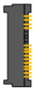
# 6.8.1. J2: Mini-PCIe Connector

Supports Mini-PCIe form factor card Supports PCIe and USB signals (from PCIe 0 and USB 4 signals on AB connector)
![The image shows a vertical, rectangular mechanical component, likely a 3D printer extruder. It features a dark grey body. On the right side, there are yellow, toothed gears arranged in a column. In the center, a black vertical strip contains white text reading 'Bondtech' stacked above 'USA'. To the far left, a dark grey rectangular block is visible.](.minibase-10r-manual-en-20171110-v1/726ebcbebc07226dd67ac49895c5dd8445c1e476f137c9ae9ebf9c2b53917341.jpg)

<table><tr><td>Pin</td><td>Signal</td><td>Pin</td><td>Signal</td></tr><tr><td>1</td><td>WAKE#</td><td>2</td><td>+ 3.3V</td></tr><tr><td>3</td><td>N.C</td><td>4</td><td>GND</td></tr><tr><td>5</td><td>N.C</td><td>6</td><td>+ 1.5V</td></tr><tr><td>7</td><td>CLKREQ#</td><td>8</td><td>N.C</td></tr><tr><td>9</td><td>GND</td><td>10</td><td>N.C</td></tr><tr><td>11</td><td>REFCLK-</td><td>12</td><td>N.C</td></tr><tr><td>13</td><td>REFCLK+</td><td>14</td><td>N.C</td></tr><tr><td>15</td><td>GND</td><td>16</td><td>N.C</td></tr><tr><td>17</td><td>N.C</td><td>18</td><td>GND</td></tr><tr><td>19</td><td>N.C</td><td>20</td><td>N.C</td></tr><tr><td>21</td><td>GND</td><td>22</td><td>PERST#</td></tr><tr><td>23</td><td>PERn</td><td>24</td><td>+ 3.3V</td></tr><tr><td>25</td><td>PERp</td><td>26</td><td>GND</td></tr><tr><td>27</td><td>GND</td><td>28</td><td>+ 1.5V</td></tr><tr><td>29</td><td>GND</td><td>30</td><td>SMB_CLK</td></tr><tr><td>31</td><td>PETn</td><td>32</td><td>SMB_DATA</td></tr><tr><td>33</td><td>PERp</td><td>34</td><td>GND</td></tr><tr><td>35</td><td>GND</td><td>36</td><td>USB_D-</td></tr><tr><td>37</td><td>GND</td><td>38</td><td>USB_D+</td></tr><tr><td>39</td><td>+ 3.3V</td><td>40</td><td>GND</td></tr><tr><td>41</td><td>+ 3.3V</td><td>42</td><td>N.C</td></tr><tr><td>43</td><td>GND</td><td>44</td><td>N.C</td></tr><tr><td>45</td><td>RSVD</td><td>46</td><td>N.C</td></tr><tr><td>47</td><td>RSVD</td><td>48</td><td>+ 1.5V</td></tr><tr><td>49</td><td>RSVD</td><td>50</td><td>GND</td></tr><tr><td>51</td><td>RSVD</td><td>52</td><td>+ 3.3V</td></tr></table>

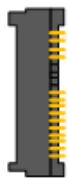
# 6.8.2. J5: Mini-PCIe/mSATA Connector

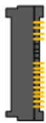
Support Mini-PCIe and mSATA form factor Support PCIe, USB and SATA signal (from PCIe 2, USB 5 and SATA 1 signals on AB connector)

For Mini-PCIe
![This image shows a vertical close-up of a black plastic electronic connector housing. On the right side, a column of yellow rectangular inserts or contacts is visible. In the center of the black plastic, the letters 'FCT' are printed vertically in white. A small black tab or latch mechanism protrudes from the left edge of the housing.](.minibase-10r-manual-en-20171110-v1/1f03ae0e23279d2491ae301bab2aea40779c997b26ba93632aeb814cb5a3140a.jpg)

<table><tr><td>Pin</td><td>Signal</td><td>Pin</td><td>Signal</td></tr><tr><td>1</td><td>WAKE#</td><td>2</td><td>+ 3.3V</td></tr><tr><td>3</td><td>N.C</td><td>4</td><td>GND</td></tr><tr><td>5</td><td>N.C</td><td>6</td><td>+ 1.5V</td></tr><tr><td>7</td><td>CLKREQ#</td><td>8</td><td>N.C</td></tr><tr><td>9</td><td>GND</td><td>10</td><td>N.C</td></tr><tr><td>11</td><td>REFCLK-</td><td>12</td><td>N.C</td></tr><tr><td>13</td><td>REFCLK+</td><td>14</td><td>N.C</td></tr><tr><td>15</td><td>GND</td><td>16</td><td>N.C</td></tr><tr><td>17</td><td>N.C</td><td>18</td><td>GND</td></tr><tr><td>19</td><td>N.C</td><td>20</td><td>N.C</td></tr><tr><td>21</td><td>GND</td><td>22</td><td>PERST#</td></tr><tr><td>23</td><td>PERn</td><td>24</td><td>+ 3.3V</td></tr><tr><td>25</td><td>PERp</td><td>26</td><td>GND</td></tr><tr><td>27</td><td>GND</td><td>28</td><td>+ 1.5V</td></tr><tr><td>29</td><td>GND</td><td>30</td><td>SMB_CLK</td></tr><tr><td>31</td><td>PETn</td><td>32</td><td>SMB_DATA</td></tr><tr><td>33</td><td>PETp</td><td>34</td><td>GND</td></tr><tr><td>35</td><td>GND</td><td>36</td><td>USB_D-</td></tr><tr><td>37</td><td>GND</td><td>38</td><td>USB_D+</td></tr><tr><td>39</td><td>+ 3.3V</td><td>40</td><td>GND</td></tr><tr><td>41</td><td>+ 3.3V</td><td>42</td><td>N.C</td></tr><tr><td>43</td><td>PCIe/mSATA_SEL</td><td>44</td><td>N.C</td></tr><tr><td>45</td><td>RSVD</td><td>46</td><td>N.C</td></tr><tr><td>47</td><td>RSVD</td><td>48</td><td>+ 1.5V</td></tr><tr><td>49</td><td>RSVD</td><td>50</td><td>GND</td></tr><tr><td>51</td><td>RSVD</td><td>52</td><td>+ 3.3V</td></tr></table>

For mSATA

![The image displays a technical diagram of an electrical connector assembly, likely a side view. Two dark grey vertical rectangular blocks flank the left and right sides, serving as housing. In the center, there are two vertical columns of yellow rectangular shapes, representing electrical contacts. These yellow contacts are separated by thin black horizontal and vertical lines. There appear to be nine contacts in each column. A black horizontal bar is visible at the very bottom of the assembly. The background is plain white. There is no text in the image.](.minibase-10r-manual-en-20171110-v1/868ed2e06986e7a2b588e05674c5cd09d93fc563e12aed3ef077307d0d55ef7b.jpg)

<table><tr><td>Pin</td><td>Signal</td><td>Pin</td><td>Signal</td></tr><tr><td>1</td><td>WAKE#</td><td>2</td><td>+ 3.3V</td></tr><tr><td>3</td><td>N.C</td><td>4</td><td>GND</td></tr><tr><td>5</td><td>N.C</td><td>6</td><td>+ 1.5V</td></tr><tr><td>7</td><td>CLKREQ#</td><td>8</td><td>N.C</td></tr><tr><td>9</td><td>GND</td><td>10</td><td>N.C</td></tr><tr><td>11</td><td>REFCLK-</td><td>12</td><td>N.C</td></tr><tr><td>13</td><td>REFCLK+</td><td>14</td><td>N.C</td></tr><tr><td>15</td><td>GND</td><td>16</td><td>N.C</td></tr><tr><td>17</td><td>N.C</td><td>18</td><td>GND</td></tr><tr><td>19</td><td>N.C</td><td>20</td><td>N.C</td></tr><tr><td>21</td><td>GND</td><td>22</td><td>PERST#</td></tr><tr><td>23</td><td>SATA_RX-</td><td>24</td><td>+ 3.3V</td></tr><tr><td>25</td><td>SATA_RX+</td><td>26</td><td>GND</td></tr><tr><td>27</td><td>GND</td><td>28</td><td>+ 1.5V</td></tr><tr><td>29</td><td>GND</td><td>30</td><td>SMB_CLK</td></tr><tr><td>31</td><td>SATA_TX-</td><td>32</td><td>SMB_DATA</td></tr><tr><td>33</td><td>SATA_TX+</td><td>34</td><td>GND</td></tr><tr><td>35</td><td>GND</td><td>36</td><td>USB_D-</td></tr><tr><td>37</td><td>GND</td><td>38</td><td>USB_D+</td></tr><tr><td>39</td><td>+ 3.3V</td><td>40</td><td>GND</td></tr><tr><td>41</td><td>+ 3.3V</td><td>42</td><td>N.C</td></tr><tr><td>43</td><td>PCIe/mSATA_SEL</td><td>44</td><td>N.C</td></tr><tr><td>45</td><td>RSVD</td><td>46</td><td>N.C</td></tr><tr><td>47</td><td>RSVD</td><td>48</td><td>+ 1.5V</td></tr><tr><td>49</td><td>RSVD</td><td>50</td><td>GND</td></tr><tr><td>51</td><td>RSVD</td><td>52</td><td>+ 3.3V</td></tr></table>

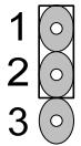
# 6.8.3. JPX8: Mini-PCIe/mSATA Selection

Select the card type for the J5 connector
![The image displays a vertical column of the numbers 1, 2, and 3 on the left side. To the right of each number is a corresponding circle aligned horizontally with it. Each circle consists of a gray outer ring surrounding a smaller, white inner circle.](.minibase-10r-manual-en-20171110-v1/6def392fe5659a705ac186cc282b1d20b2834b26cbcb9e258e5b612a33f54adb.jpg)

<table><tr><td>Jumper</td><td>Status</td></tr><tr><td>1-2</td><td>Mini-PCIe &lt;&lt;&lt;</td></tr><tr><td>2-3</td><td>mSATA</td></tr></table>

# 6.9. SATA

# 6.9.1. J9: SATA

Drive activity is indicated by LED D3 (see 8.3 Indicator LEDs on page 34)

![A black and white line drawing of a simple house facade. It features a rectangular door on the left side with a small square detail, and a window on the right side divided by a horizontal bar. Above the structure is a flat roof outline with a small, vertical rectangular shape resembling a chimney on the right.](.minibase-10r-manual-en-20171110-v1/967a15238316f3494969c9ad59f673f0190909d0c174abff5350b5794a62ce04.jpg)

<table><tr><td>Pin</td><td>Signal</td></tr><tr><td>1</td><td>GND</td></tr><tr><td>2</td><td>Tx+</td></tr><tr><td>3</td><td>Tx-</td></tr><tr><td>4</td><td>GND</td></tr><tr><td>5</td><td>Rx-</td></tr><tr><td>6</td><td>Rx+</td></tr><tr><td>7</td><td>GND</td></tr></table>

# 6.9.2. JX9: Power for SATA

![The image displays a graphic featuring black lines forming a bracket-like shape with segments on the left and a larger vertical and bottom line on the right. Inside this enclosure, three grey squares are stacked vertically.](.minibase-10r-manual-en-20171110-v1/28f38a388a3ec028ad6baa58f2cf6082d0189cf7ac169d6a2d821822aecdfd87.jpg)

<table><tr><td>Pin</td><td>Signal</td></tr><tr><td>1</td><td>+ 5.0V</td></tr><tr><td>2</td><td>GND</td></tr></table>

Note: &lt;&lt;&lt;&lt; indicates default setting

# 6.10. USB and LAN

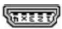
# 6.10.1. J10: Mini-USB

Supports Mini-USB form factor (from USB 7 signals on AB connector)
![The image displays a monochrome logo featuring the text 'FLEXFIT' in a bold, block-style sans-serif font. The letters are heavily outlined with a white fill and black stroke, creating a 3D or embossed effect. The text is centered inside a thick, rounded rectangular border that resembles a label or patch.](.minibase-10r-manual-en-20171110-v1/9979f0732fab5c7f9d904a4d0bfd9892ffb165f976546690388f3149ba576318.jpg)

&lt;table&gt;<tr><td>Pin</td><td>Signal</td></tr><tr><td>1</td><td>Client_PWR_Dectect</td></tr><tr><td>2</td><td>USB-</td></tr><tr><td>3</td><td>USB+</td></tr><tr><td>4</td><td>N.C.</td></tr><tr><td>5</td><td>GND</td></tr></table>

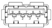
# 6.10.2. J13: USB 3.0 x 2

USB 2.0 compatible (from USB 0, USB\_SS0, USB 1, USB\_SS1 signals on AB connector)
![The image displays a line drawing of a rectangular electronic component, likely a DIP switch or similar connector. Inside the main rectangular outline, the numbers '9 8 7 6 5' are arranged in a row near the top, and the number '4' is centered below that row. Above the main rectangle, there are two small rectangular shapes on the far left and two on the far right. Below the main rectangle, there is a horizontal row of five small rectangular shapes.](.minibase-10r-manual-en-20171110-v1/89637ce8c2f393fbf62966b9d9d96519e85de7cfa5f9939d0ca05c722ab5c7b8.jpg)

<table><tr><td>Pin</td><td>Signal</td></tr><tr><td>1</td><td>USB3_P5VA</td></tr><tr><td>2</td><td>USB2_CMAN</td></tr><tr><td>3</td><td>USB2_CMAP</td></tr><tr><td>4</td><td>GND</td></tr><tr><td>5</td><td>USB3A_CMRXN</td></tr><tr><td>6</td><td>USB3A_CMRXP</td></tr><tr><td>7</td><td>GND</td></tr><tr><td>8</td><td>USB3A_CMTXN</td></tr><tr><td>9</td><td>USB3A_CMTXP</td></tr></table>

# 6.10.3. JX14: USB 2.0 x 2 and GbE RJ-45

USB from USB 2, USB 3, signals on AB Connector GbE from Intel® i210 using PCIe x1 signals on AB connector)
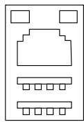
![The image is a black and white line drawing depicting a vertical rectangular panel or interface. At the very top, there are two small, empty squares positioned at the left and right sides. In the center is a large, rectangular shape with a stepped, staircase-like upper edge. Below this central shape are two horizontal rows stacked vertically; each row consists of a long rectangle containing four smaller squares arranged in a horizontal line.](.minibase-10r-manual-en-20171110-v1/b54e991bf0fec2a7dbecf04b8f9b20111a5659097b9a2dace1197d32519f3b72.jpg)

<table><tr><td>Pin</td><td>Signal (USB)</td></tr><tr><td>1</td><td>+ 5V</td></tr><tr><td>2</td><td>USB-</td></tr><tr><td>3</td><td>USB+</td></tr><tr><td>4</td><td>GND</td></tr></table>

# 6.10.4. JX3: GbE RJ-45

From GbE signals on AB connector
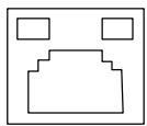
![The image displays a black and white line drawing of a large rectangle. Inside the top section, there are two smaller, separate rectangles positioned side-by-side. In the center, below these rectangles, is a larger shape with a flat bottom and vertical sides that form a stepped profile at the top.](.minibase-10r-manual-en-20171110-v1/c7f09571e587242bec926f39f10410cb6ead895b0784d4abefb73fcd60732a14.jpg)

<table><tr><td>Pin</td><td>Signal</td></tr><tr><td>1</td><td>BI_DA+</td></tr><tr><td>2</td><td>BI_DA-</td></tr><tr><td>3</td><td>BI_DB+</td></tr><tr><td>4</td><td>BI_DB-</td></tr><tr><td>5</td><td>BI_DC+</td></tr><tr><td>6</td><td>BI_DC-</td></tr><tr><td>7</td><td>BI_DD+</td></tr><tr><td>8</td><td>BI_DD-</td></tr></table>

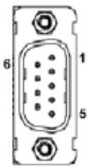
# 6.11. Serial Ports

J3: COM 1

J6: COM 2

Only TX/RX support
![The image displays a line drawing of a DB6 D-sub connector. It features a vertical rectangular housing with threaded screw terminals at the top and bottom. Centered within the housing is a D-shaped metal shield outline containing six circular contact points arranged in two vertical columns of three.\n\nThe text labels are:\n*   **'6'** on the left side.\n*   **'1'** on the right side, near the top.\n*   **'5'** on the right side, near the bottom.](.minibase-10r-manual-en-20171110-v1/3daff3a3943c328cb6619e3ed4b968a7471a91928dc3531db32cf8b45468ae16.jpg)

<table><tr><td>Pin</td><td>Signal</td><td>Pin</td><td>Signal</td></tr><tr><td>1</td><td>N.C.</td><td>2</td><td>RXD</td></tr><tr><td>3</td><td>TXD</td><td>4</td><td>N.C.</td></tr><tr><td>5</td><td>GND</td><td>6</td><td>N.C.</td></tr><tr><td>7</td><td>N.C.</td><td>8</td><td>N.C.</td></tr><tr><td>9</td><td>N.C.</td><td></td><td></td></tr></table>

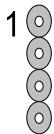
# 6.12. ${ \mathsf { I } } ^ { 2 } { \mathsf { C } } ,$ SMBus and CAN Bus

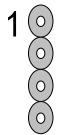
# 6.12.1. H2: I2C Bus
![The image displays two identical vertical columns side-by-side. Each column consists of the number '1' positioned at the top, followed by a vertical stack of four grey circles.](.minibase-10r-manual-en-20171110-v1/19caa28e3a0fcf6d65a827b31898c71ccaf2e6c1268f0713f8cccd0e800968ab.jpg)

<table><tr><td>Pin</td><td>Signal</td></tr><tr><td>1</td><td>+ 3.3V</td></tr><tr><td>2</td><td>I2C_DAT</td></tr><tr><td>3</td><td>I2C_CK</td></tr><tr><td>4</td><td>GND</td></tr></table>

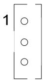
# 6.12.2. H1: SM Bus

![1\nA vertical column of four grey rings.](.minibase-10r-manual-en-20171110-v1/b9e07a42015375a7329236c584b3a9e23beb6a56f219bae28d268d26d4ccd1f5.jpg)

<table><tr><td>Pin</td><td>Signal</td></tr><tr><td>1</td><td>+ 3.3V</td></tr><tr><td>2</td><td>SMB_DAT</td></tr><tr><td>3</td><td>SMB_CLK</td></tr><tr><td>4</td><td>GND</td></tr></table>

# 6.12.3. JX10: CAN Bus

![The image shows a minimalist line drawing of a refrigerator with two doors. The top door, likely a freezer, has a small handle on the left. The larger bottom door has a similar handle on the left and three small circles arranged vertically in the center. There is no text.](.minibase-10r-manual-en-20171110-v1/73f84d68c4ffae3e6086b48bf5644b45d46df062b6895e90ee3cdfd448fbc640.jpg)

<table><tr><td>Pin</td><td>Signal</td></tr><tr><td>1</td><td>TX</td></tr><tr><td>2</td><td>RX</td></tr><tr><td>3</td><td>GND</td></tr></table>

# 6.13. Fan Connector

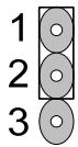
# 6.13.1. JPX4: Fan Type Selection

Selects 4-pin or 3-pin type fan
![The image displays the numbers 1, 2, and 3 arranged vertically in black text on the left side. To the right of each number is a corresponding grey circle with a white center, stacked vertically in a column.](.minibase-10r-manual-en-20171110-v1/dd494a687574177b20450dc2df9fbb6989299eb1d27a9ca783561d2f85355fd0.jpg)

<table><tr><td>Jumper</td><td colspan="2">Status</td></tr><tr><td>1-2</td><td>4P FAN</td><td>&lt;&lt;&lt;&lt;</td></tr><tr><td>2-3</td><td>3P FAN</td><td></td></tr></table>

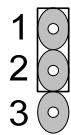
# 6.13.2. JPX5: Fan Control

Only available for 3-pin fan
![The image displays three horizontal rows against a white background. On the left side, the numerals '1', '2', and '3' appear vertically in a large, bold, black font. To the right of each number is a corresponding vertical stack of identical grey circular objects that resemble washers, featuring a dark grey outer ring and a lighter grey center. Specifically, the top row shows one circle next to the number 1, the middle row shows two stacked circles next to the number 2, and the bottom row shows three stacked circles next to the number 3.](.minibase-10r-manual-en-20171110-v1/f91fdffa41700d776e2a6d1dcd77642c0b404b939eb5ce125d9e5fd56509aacd.jpg)

<table><tr><td>Jumper</td><td>Status</td></tr><tr><td>1-2</td><td>Full ON &lt;&lt;&lt;</td></tr><tr><td>2-3</td><td>PWM CTRL</td></tr></table>

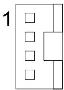
# 6.13.3. H3: Fan Header

![The image displays a simple black-and-white line drawing. On the far left, the number '1' is shown in a large, bold font. To the right of the number, there is a vertical column of four empty square outlines. Further to the right, there is a rectangle positioned next to two parallel vertical lines that run down the side.](.minibase-10r-manual-en-20171110-v1/cac0f802ad242a18f160219a64798edd38cb8c8a8c5bdd398ce003ca99e939fa.jpg)

<table><tr><td>Pin</td><td>Signal</td></tr><tr><td>1</td><td>Speed_Control (PWM)</td></tr><tr><td>2</td><td>Speed Sense</td></tr><tr><td>3</td><td>PWR (5V)</td></tr><tr><td>4</td><td>GND</td></tr></table>

Note: &lt;&lt;&lt;&lt; indicates default setting

# 6.14. Other Connectors

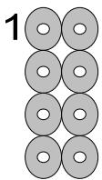
# 6.14.1. JPX6: EXT GPIO

Note: address is 42h
![The image displays the number 1 in black on the left side. To its right is a grid of ten grey rings arranged in two columns of four rows each.](.minibase-10r-manual-en-20171110-v1/725eb70f3b484dbd5ec0a712b32abef8a1a741100c77794cbea2f14639af697a.jpg)

&lt;table&gt;<tr><td>Pin</td><td>Signal</td><td>Pin</td><td>Signal</td></tr><tr><td>1</td><td>GPI_0</td><td>2</td><td>GPO_0</td></tr><tr><td>3</td><td>GPI_1</td><td>4</td><td>GPO_1</td></tr><tr><td>5</td><td>GPI_2</td><td>6</td><td>GPO_2</td></tr><tr><td>7</td><td>GPI_3</td><td>8</td><td>GPO_3</td></tr></table>

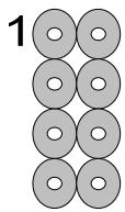
# 6.14.2. JPY1: GPIO

From GPIO signal on AB connector Note: address is 40h
![The image features a black vertical column on the left containing the white numeral '1'. To the right of this column is a grid of eight identical grey rings with white centers, arranged in four rows and two columns.](.minibase-10r-manual-en-20171110-v1/f557a0301e1f18d1d3dc4f989a8ca106155134a5c2ae3a755fe997b12653ce7b.jpg)

<table><tr><td>Pin</td><td>Signal</td><td>Pin</td><td>Signal</td></tr><tr><td>1</td><td>GPI_0</td><td>2</td><td>GPO_0</td></tr><tr><td>3</td><td>GPI_1</td><td>4</td><td>GPO_1</td></tr><tr><td>5</td><td>GPI_2</td><td>6</td><td>GPO_2</td></tr><tr><td>7</td><td>GPI_3</td><td>8</td><td>GPO_3</td></tr></table>

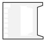
# 6.14.3. J7: SD Card Slot

From SD signal on AB connector
![The image displays a simple line drawing inside a rectangular border. Inside the rectangle, a vertical line runs down slightly to the left of the center. To the left of this vertical line, there are several faint, light gray vertical lines resembling text. To the right of the vertical line, there is a 'U' shaped line, consisting of a vertical segment, a horizontal bottom segment, and another vertical segment going up.](.minibase-10r-manual-en-20171110-v1/7ece743229540589052cc4e6365397364b19c86aee6475154e6d68cdd6feaa1e.jpg)

# 6.14.4. UX4: Secondary SPI BIOS Socket

JPX7: BIOS Selection
![The image features a vertical block of text on the left side next to a black-and-white graphic of a stylized hard drive platter on the right. The text reads:\n\nA hard drive consists of one or more\nspinning disks made of aluminum\nglass or ceramic coated with a\nlayer of magnetic material.](.minibase-10r-manual-en-20171110-v1/6f92f1888acfec108e421287a63cb71e7a4cfd55fabf440d28ea57ae7617e010.jpg)

<table><tr><td>Pin</td><td>Signal</td></tr><tr><td>1</td><td>CS#</td></tr><tr><td>Pin</td><td>Signal</td></tr><tr><td>1-2</td><td>Module BIOS</td></tr><tr><td>3</td><td>WR#&lt;</td></tr><tr><td>4 2-3</td><td>Carrier BIOS</td></tr><tr><td></td><td>GND</td></tr><tr><td>5</td><td>DI</td></tr><tr><td>6</td><td>CLK</td></tr><tr><td>7</td><td>HOLD#</td></tr><tr><td>8</td><td>+ 3.3V</td></tr></table>

# 6.14.5. H5: CPLD\_JTAG

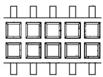
![This is a black-and-white line drawing depicting a schematic grid structure. The central portion consists of ten squares arranged in two rows of five columns. Each square in the grid is drawn with a double outline, appearing as a smaller square inside a larger one.\n\nAbove the top row of squares, there is a horizontal line with five small, vertical rectangular shapes positioned on top of it. Below the bottom row of squares, there is a similar horizontal line with five small, vertical rectangular shapes hanging below it. These rectangular shapes on the top and bottom appear aligned with the columns of the central grid.](.minibase-10r-manual-en-20171110-v1/ed26d31d9a1f66e97f604b83a47f93395ef8e2d2ae6ac5497c5f1eccaf0406e2.jpg)

<table><tr><td>Pin</td><td>Signal</td></tr><tr><td>1</td><td>CPLD_TCKL</td></tr><tr><td>2</td><td>GND</td></tr><tr><td>3</td><td>CPLD_TDO</td></tr><tr><td>4</td><td>+ 3.3V</td></tr><tr><td>5</td><td>CPLD_TMS</td></tr><tr><td>6</td><td>N.C.</td></tr><tr><td>7</td><td>N.C.</td></tr><tr><td>8</td><td>N.C.</td></tr><tr><td>9</td><td>CPLD_TDI</td></tr><tr><td>10</td><td>GND</td></tr></table>

# 6.15. Other Jumpers

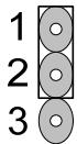
# 6.15.1. JP4: Clear CMOS

To clear CMOS, shut down the power and short pins 2 and 3
![The image displays a vertical list of three items. On the left side of each row is a number in bold black font: '1' at the top, '2' in the middle, and '3' at the bottom. To the right of each number is a grey circle with a black outline. Inside each circle is a white horizontal rectangle in the center, resembling a USB connector symbol. The numbers are horizontally aligned with their respective circles.](.minibase-10r-manual-en-20171110-v1/a4d91283a1bc0161fcdce5ae4f0214ff22461a44d19dfdd0a78b0882c68aaedd.jpg)

<table><tr><td>Pin</td><td>Signal</td></tr><tr><td>1-2</td><td>Normal &lt;&lt;&lt;</td></tr><tr><td>2-3</td><td>Clear CMOS</td></tr></table>

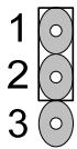
# 6.15.2. JPX7: BIOS Selection

See 7.1 SPI Secondary BIOS on page 31 for a detailed description.
![The image displays a vertical column of black numbers on the left side: 1, 2, and 3. To the right of each number is a corresponding grey ring with a white center, arranged in a vertical column. The numbers are horizontally aligned with the respective rings.](.minibase-10r-manual-en-20171110-v1/d7a692b36c575d6ff796e140ba24abdbe8bae2f18c2ee4aef20dda5ff2ae109c.jpg)

<table><tr><td>Pin</td><td>Signal</td></tr><tr><td rowspan="2">1-2</td><td>Module BIOS</td></tr><tr><td>&lt;&lt;&lt;&lt;</td></tr><tr><td>2-3</td><td>Carrier BIOS</td></tr></table>

Note: &lt;&lt;&lt;&lt; indicates default setting

# 6.16. Power Connectors

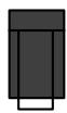
# 6.16.1. JX5: AC Adapter

For 19V AC adapter (current: 4.7A)
![This is a black-and-white line drawing of a vertical rectangular assembly. The top section is a large, dark grey rectangle containing a thinner, lighter rectangular outline. Below this main block is a smaller, lighter rectangular outline resembling a ring. A thin, vertical black bar runs parallel along the right side of the component.](.minibase-10r-manual-en-20171110-v1/9cdd7b06d1e851833e0c7fe187e08cfb212ae05a6326a7be5d370ce81e865fb9.jpg)

# 6.16.2. H4/H7: Smart Battery 1/2 Connectors

Supports dual Smart Batteries

![A vertical column of ten empty square checkboxes arranged one above the other, enclosed in a frame with a thick black border on the right and a thin border on the left.](.minibase-10r-manual-en-20171110-v1/bf464ca671144d9beb0135aa3af5d686ea50e72d445b74964e3e27abdf7d070a.jpg)

&lt;table&gt;<tr><td>Pin</td><td>Signal</td></tr><tr><td>1</td><td>PWR</td></tr><tr><td>2</td><td>PWR</td></tr><tr><td>3</td><td>PWR</td></tr><tr><td>4</td><td>SMBus_Clk</td></tr><tr><td>5</td><td>SMBus_Dat</td></tr><tr><td>6</td><td>Thermistor</td></tr><tr><td>7</td><td>GND</td></tr><tr><td>8</td><td>GND</td></tr><tr><td>9</td><td>GND</td></tr></table>

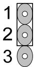
# 6.16.3. JPY2: Smart Battery Configuration

Select 3-cell or 2-cell battery configuration
![The image displays three rows of content arranged vertically. On the left side, the numbers **1**, **2**, and **3** appear in a large, bold, black font. On the right side, aligned with each number, is a grey circle containing a small black dot in its center.](.minibase-10r-manual-en-20171110-v1/7c8712e633dad55c039417bd572ac6207a624024b721d3c568803f8b5519b370.jpg)

<table><tr><td>Pin</td><td colspan="2">Signal</td></tr><tr><td>1-2</td><td>3 Cell</td><td>&lt;&lt;&lt;&lt;</td></tr><tr><td>2-3</td><td>2 Cell</td><td></td></tr></table>

# 6.16.4. JPX1: Protection Selection

![The image displays a vertical column of three grey, pill-shaped buttons stacked directly on top of each other. To the left of this column, the numbers '1', '2', and '3' appear in black text, each aligned with the corresponding button from top to bottom. Each grey button features a lighter grey circle in its center.](.minibase-10r-manual-en-20171110-v1/af873c020c669d64f12fa018f79c4e8b9fc21a44c7aaff32053c9ff4b93f6b7c.jpg)

<table><tr><td>Pin</td><td>Signal</td></tr><tr><td>1-2</td><td>2 Cell</td></tr><tr><td>2-3</td><td>3 Cell &lt;&lt;&lt;&lt;</td></tr></table>

Note: &lt;&lt;&lt;&lt; indicates default setting

# 6.17. Power Jumper Settings

# 6.17.1. JPX2: AT/ATX Mode

In AT mode, JPX2 shorts PS\_ON# to ground directly to force power on.

&lt;table&gt;<tr><td>Pin</td><td colspan="2">Signal</td></tr><tr><td>1-2</td><td>ATX</td><td>&lt;&lt;&lt;&lt;</td></tr><tr><td>2-3</td><td>AT</td><td></td></tr></table>

# 6.17.2. JPX3: 5VSB to Module Source

![The image features three rounded rectangles stacked vertically. To the left of each rectangle is a bold black number, reading 1, 2, and 3 from top to bottom. Inside each rectangle is a grey circle with a white center.](.minibase-10r-manual-en-20171110-v1/86e176b63a3d0c33bb1c1846ac91933857ae5e45671881be1c40fa0f31ed178c.jpg)

<table><tr><td>Pin</td><td>Signal</td></tr><tr><td rowspan="2">1-2</td><td>w/ 5VSB</td></tr><tr><td>&lt;&lt;&lt;&lt;</td></tr><tr><td>2-3</td><td>w/o 5VSB</td></tr></table>

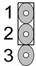
# 6.17.3. JP1: PS\_ON# Signal Source

All ADLINK modules support S3 mode and subsequent power down of the ATX power supply. For modules that connect the S3 signal, PS\_ON# should always be set to SUS\_S3# as source (even when S3 mode is disabled in the BIOS). For modules that do not bring out the S3 signal, PS\_ON# should be set to SUS\_S5# as source.
![The image displays a vertical column of the numbers 1, 2, and 3 aligned on the left side. To the right of each number is a corresponding grey circle with a white inner ring, stacked vertically in a column.](.minibase-10r-manual-en-20171110-v1/07c76081eb24fb2fbf2aedaa399bb2a6041c250127c93540919250cf257e1632.jpg)

<table><tr><td>Pin</td><td>Signal</td></tr><tr><td rowspan="2">1-2</td><td>SUS_S3#</td></tr><tr><td>&lt;&lt;&lt;&lt;</td></tr><tr><td>2-3</td><td>SUS_S5#</td></tr></table>

Note: &lt;&lt;&lt;&lt; indicates default setting

This page intentionally left blank.

# 7. Secondary BIOS

The miniBASE-10R supports Secondary BIOS using Serial Peripheral Interface (SPI) for COM.0 Rev. 3.0 modules.

Secondary BIOS solutions can be used as an alternative to the on-module BIOS and provide support for the following:

Testing new BIOS versions
Development of firmware modifications
Recovery if soldered BIOS on module is corrupted

# 7.1. SPI Secondary BIOS

SPI is supported by PICMG COM.0 Rev. 2.0 to provide a secondary BIOS for COM Express Rev 2.0 modules that support a SPI Secondary BIOS.

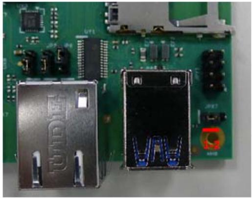
To use the BIOS on the module:

Short pins 1-2 on JPX7
![Close-up of electronic components on a green printed circuit board (no visible text or symbols)](.minibase-10r-manual-en-20171110-v1/5f53ec5ddf17ced8a72cc6b5036a3b0fe206b4c211255eef0adf9ec46cc1f279.jpg)

To use the SPI BIOS on the carrier board:

Short pins 2-3 on JPX7
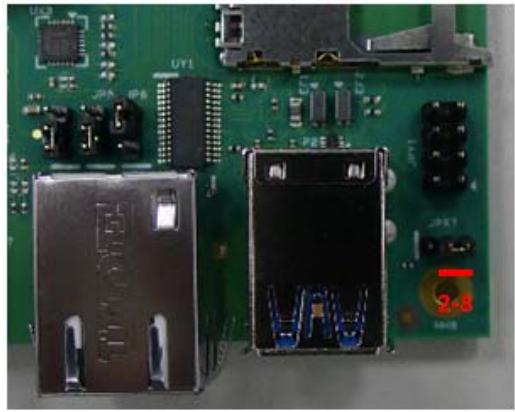
![Close-up of a green printed circuit board with electronic components and connectors (no readable text or symbols)](.minibase-10r-manual-en-20171110-v1/84183bdd03f2e9b5c493b3094a94cbfb9de7a583488a327e1935f849a3d2c0d4.jpg)

This page intentionally left blank.

# 8. Switches, POST and LEDs

# 8.1. Switches (S1-S4)

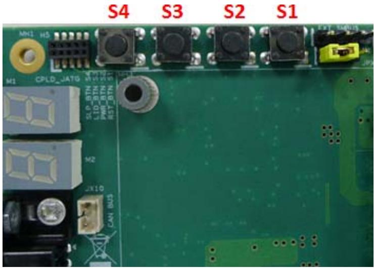
There are four switches on the miniBASE-10R.

S1 switch is the Reset Button.
S2 switch is the Power Button.

S3 switch is the Lid Button. It supports Type 10 modules for ACPI power management behavior setting in OS.

S4 switch is the Sleep Button. It supports Type 10 modules for ACPI power management behavior setting in OS.
![S4 S3 S2 S1\nMN1 H5\nM1 CPLD_JATG\nSLP_DTN\nL1D_DTN\nPWM_DTN\nRST_DTN\nM2\nJX10\nCAN BN3](.minibase-10r-manual-en-20171110-v1/b1a479377dcd96f298a0957778e30072c74d97bfb569de5ac184f479bc37e4de.jpg)

# 8.2. POST

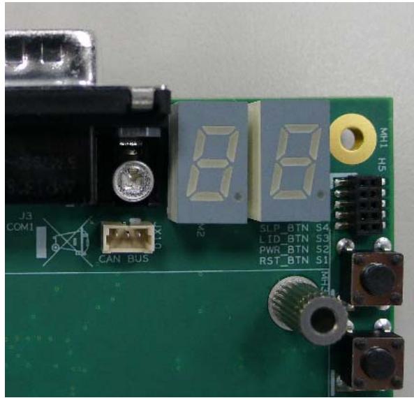
An LPC based POST display is added for debugging. The two LEDs display the actual POST data.
![Close-up of a green printed circuit board with electronic components and a large display showing '8.8' (no readable text or symbols beyond basic markings)](.minibase-10r-manual-en-20171110-v1/8abc9f3b39f571b4e3f07b851a8c22296369035e7fbefa6158150a722947c41f.jpg)

# 8.3. Indicator LEDs

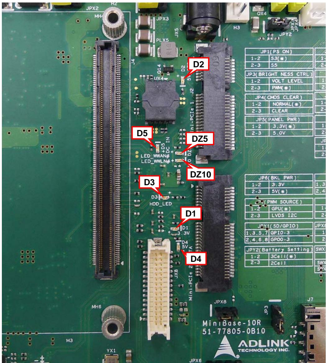
There are seven indicator LEDs located on the front side of the board as follows:
![JPX2\nH2\nMH4\nJPX3\nPLX5\nJX5\nQ14\nUX4\nD2\n5V\nD2\nD5\nDZ5\nLED_WWAN#\nLED_WWLN#\nD1\n3.3V\nD3\nD4\nMini-PCIe 2\nJX8\nJX6\nM3\nYX1\nJPX6\nJPY2(PS ON)\n1-2 S3(*)\n2-3 S5\nJP3(BRIGHT NESS CTRL)\n1-2 VOLT LEVEL\n2-3 PWM(*)\nJP4(CMOS CLEAR)\n1-2 NORMAL(*)\n2-3 CLEAR\nJP5(PANEL PWR)\n1-2 3.3V(*)\n2-3 5.0V\nJP6(BKL PWR)\n1-2 3.3V\n2-3 5V(*)\nJP7(PWM SOURCE)\n1-2 GPU(*)\n2-3 LVDS I2C\nJPY1(SD/GPIO)\n1,3,5,7 GPIO-3\n2,4,6,8 GPOO-3\nJPY2(Battery Setting)\n1-2 3Cell(*)\n2-3 2Cell\nSWX\nSWX\nSWX\nJPX8\nJP3\nJ7\nMiniBase-10R\n51-77805-0B10\nADLINK\nTECHNOLOGY INC.](.minibase-10r-manual-en-20171110-v1/328a0edbf9c3b82f67903b8b89f055d5f2fb457c6323386e7e0420e371a00060.jpg)

D1: indicates 3.3V power for carrier board
z D2: indicates 5VSB power for carrier board and COM Express module
D3: indicates SATA drive activity (connector J9)
z D4: indicates 5V power for carrier board
D5: indicates 19VDC power adapter is plugged in
DZ5: indicates the insertion of WWAN card on mini-PCIe 1 slot
z DZ10: indicates the insertion of WLAN card on mini-PCIe 1 slot

# 9. Smart Battery Management System

The miniBASE-10R integrates a Smart Battery Management System that supports dual Smart Batteries and a 19V adapter. The adapter connects to miniBASE-10R through a standard 2.5mm input jack. The battery charger output voltage is configurable to adapt it to battery packs consisting of 2 or 3 Li-ion battery cells.\*

\*Note: ADLINK Starter Kit battery packs with 2 cells provide 5.7VDC to 8.4VDC output to the COM Express module. The reference battery packs with 3 cells provide 9VDC to 12.6VDC output to the COM Express module. Please ensure that the COM Express module supports Wide Voltage Input power.

# 9.1. Input Power

&lt;table&gt;<tr><td></td><td>AD/DC Adapter Input</td><td>Battery*</td></tr><tr><td>Voltage</td><td>19V</td><td>2 cells: 5.7VDC - 8.4VDC3 cells: 9VDC - 12.6VDC</td></tr><tr><td>Max. Current</td><td>4.7A</td><td>Dependent on battery</td></tr><tr><td>Power</td><td>90W</td><td>N.A.</td></tr></table>

\*Note: The optional reference battery packs provided with miniBASE-10R have 3 cells in series or 2 cells in series.

# 9.2. Charger Output Capability

<table><tr><td></td><td>Charger</td></tr><tr><td>Voltage</td><td>12.6V (3cell)8.4V (2cell)</td></tr><tr><td>Max. Current</td><td>4.0 A</td></tr></table>

# 9.3. Key Characteristics

z Simultaneous Dual Charging: charges two Smart Batteries simultaneously to reduce charging time
Simultaneous Discharging: simultaneous dual discharge increases battery operating time by reducing internal battery losses due to high discharge rate

# 9.4. Battery Settings

See 6.16 Power Connectors and 6.17 Power Jumper Settings for detailed information.

# 9.5. Windows OS Interface

# 9.5.1. Device Presence

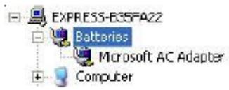
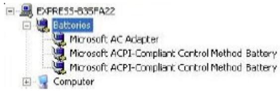
ADLINK COM Express Type 10 modules feature a BIOS that fully supports all Smart Battery communications using existing interfaces defined in the COM Express specification and are fully compatible with the integrated Smart Battery Management System. The BIOS reports the presence of a Smart Battery device to the OS. In Windows, the battery power subsystem information is listed in the Device Manager under the "Batteries" category. The system BIOS will check the current system configuration and then report back to the OS. There are three possibilities for the battery report information.

# 9.5.2. No Battery Power Subsystem Present

The system BIOS checks for the presence of a charger, selector or system manager. If there is no device attached, it will only report the presence of an AC adapter to the OS.
![EXPRESS-B35FA22\nBatteries\nMicrosoft AC Adapter\nComputer](.minibase-10r-manual-en-20171110-v1/153e1f12d0937d8a7540499ad513e2243704def484b51440a6e1183571676c39.jpg)

# 9.5.3. Battery Present

The system BIOS will report an AC adapter and two battery devices to the OS
![EXPRESS-835PA22\nBatteries\nMicrosoft AC Adapter\nMicrosoft ACPI-Compliant Control Method Battery\nMicrosoft ACPI-Compliant Control Method Battery\nComputer](.minibase-10r-manual-en-20171110-v1/8b7542c8870dd02c5a46d5fb5c55315ae4eb28d37cd35bcb1f64a3e2b567ab66.jpg)

# 9.5.4. Battery State Notification

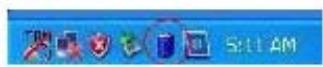
The system BIOS is notified of the state (AC power or battery mode) when it receives an SMBALERT# as a SCI event. An alert may be sent to update the charging state, remaining battery capacity, or presence of an AC adapter. The OS can also query the system BIOS to update the battery power information. Placing the cursor over the battery state icon will cause the OS to update the battery power information.

When an AC adapter is inserted or removed, the battery state icon in the taskbar will change to indicate the current state. To display the battery state icon in the taskbar, enable the option "Always show icon on the taskbar" from the "Advanced" tab of "Power Options Properties".

![The image displays a horizontal section of a computer interface, likely a taskbar, with a blue gradient background. On the left, a row of icons is visible. From left to right, they appear to be a crossed-out document icon, a shield with a globe, a green shield icon, a red shield icon, a purple book icon (which is circled in red), and a blue book or folder icon. On the far right side, white text reads '5:11 AM'.](.minibase-10r-manual-en-20171110-v1/34926cdbc02d5956272e31ac46b9079dc7086c12bf863624f154b67da788cdfc.jpg)

![The image displays a cropped section of a computer taskbar's notification area, featuring a bright blue background. On the far left, a small, blurry icon is partially visible. In the center, a row of system tray icons is shown, with one specific icon circled in blue ink; this icon appears to represent a network connection (a computer and cable). To the right of the circled icon are several other icons, including a red symbol and a blue square icon. On the far right, the time is displayed in white text: '5:57 AM'.](.minibase-10r-manual-en-20171110-v1/0f7015cce6b1f27c51d7ea7cf483af262836f54226e06d84e8aca88995143b06.jpg)

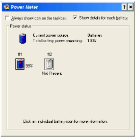
# 9.5.5. Battery Information

To view detailed battery status information, double-click on the battery or AC adapter icon.
![Power Meter\nAlways show icon on the taskbar. Show details for each battery.\nPower status\nCurrent power source: Batteries\nTotal battery power remaining: 100%\n#1 #2\n55% Not Present\nClick an individual battery icon for more information.](.minibase-10r-manual-en-20171110-v1/58307db755f278da278c668a2510295baebdbad5af340c3dd077a32ffcb17894.jpg)

# Safety Instructions

Read and follow all instructions marked on the product and in the documentation before you operate your system. Retain all safety and operating instructions for future use.

Please read these safety instructions carefully.
• Please keep this User‘s Manual for later reference.
The equipment should be operated only from the type of power source indicated on the rating label. Make sure the voltage of the power source when connect the equipment to the power outlet.
• If your equipment has a voltage selector switch, make sure that the switch is in the proper position for your area. The voltage selector switch is set at the factory to the correct voltage.
• For pluggable equipment, that the socket-outlet shall be installed near the equipment and shall be easily accessible.
• Place the power cord such a way that people can not step on it. Do not place anything over the power cord.
• If the equipment is not use for long time, disconnect the equipment from mains to avoid being damaged by transient overvoltage.
• All cautions and warnings on the equipment should be noted.
Please keep this equipment from humidity.
• Do not use this equipment near water or a heat source.
• Lay this equipment on a reliable surface when install. A drop or fall could cause injury.
Never pour any liquid into opening; this could cause fire or electrical shock.
Openings in the case are provided for ventilation. Do not block or cover these openings. Make sure you provide adequate space around the system for ventilation when you set up your work area. Never insert objects of any kind into the ventilation openings.
• To avoid electrical shock, always unplug all power cables and modem cables from the wall outlets before removing covers.
Lithium Battery provided (real time clock battery)

# CAUTION – Risk of explosion if battery is replaced with one of an incorrect type. Dispose of used batteries according to the instructions

• If one of the following situations arises, get the equipment checked by a service personnel:

 The power cord or plug is damaged.
 Liquid has penetrated into the equipment.
 The equipment has been exposed to moisture.
 The equipment has not work well or you can not get it work according to user‘s manual.
 The equipment has dropped and damaged.
 If the equipment has obvious sign of breakage.

# Getting Service

Ask an Expert: http://askanexpert.adlinktech.com

# ADLINK Technology, Inc.

<table><tr><td>Address:</td><td>9F, No.166 Jian Yi Road, Zhonghe District New Taipei City 235, Taiwan</td></tr><tr><td>Tel:</td><td>+886-2-8226-5877</td></tr><tr><td>Fax:</td><td>+886-2-8226-5717</td></tr><tr><td>Email:</td><td>service@adlinktech.com</td></tr></table>

# Ampro ADLINK Technology, Inc.

Address: 5215 Hellyer Avenue, #110, San Jose, CA 95138, USA

Tel: +1-408-360-0200

Toll Free: +1-800-966-5200 (USA only)

Fax: +1-408-360-0222

Email: info@adlinktech.com

# ADLINK Technology (China) Co., Ltd.

Address: 300 Fang Chun Rd., Zhangjiang Hi-Tech Park, Pudong New Area Shanghai, 201203 China

Tel: +86-21-5132-8988

Fax: +86-21-5132-3588

Email: market@adlinktech.com

# LiPPERT ADLINK Technology GmbH

Address: Hans-Thoma-Strasse 11, D-68163, Mannheim, Germany

Tel: +49-621-43214-0

Fax: +49-621 43214-30

Email: emea@adlinktech.com

Please visit the Contact page at www.adlinktech.com for information on how to contact the ADLINK regional office nearest you.
[🔗 Link to the original document](.minibase-10r-manual-en-20171110-v1/minibase-10r-manual-en-20171110-v1.pdf)