# MXM-AXe
User’s Guide
intel
Revision History
| Revision | Description | Date | Author |
| 0.1 | Preliminary release | 2023-07-31 | CC |
# Preface
# Disclaimer
Information in this document is provided in connection with ADLINK products. No license, express or implied, by estoppel or otherwise, to any intellectual property rights is granted by this document. Except as provided in ADLINK´s Terms and Conditions of Sale for such products, ADLINK assumes no liability whatsoever, and ADLINK disclaims any express or implied warranty, relating to sale and/or use of ADLINK products including liability or warranties relating to fitness for a particular purpose, merchantability, or infringement of any patent, copyright or other intellectual property right. If you intend to use ADLINK products in or as medical devices, you are solely responsible for all required regulatory compliance, including, without limitation, Title 21 of the CFR (US), Directive 2007/47/EC (EU), and ISO 13485 & 14971, if any. ADLINK may make changes to specifications and product descriptions at any time, without notice.
# Environmental Responsibility
ADLINK is committed to fulfil its social responsibility to global environmental preservation through compliance with the European Union's Restriction of Hazardous Substances (RoHS) directive and Waste Electrical and Electronic Equipment (WEEE) directive. Environmental protection is a top priority for ADLINK. We have enforced measures to ensure that our products, manufacturing processes, components, and raw materials have as little impact on the environment as possible. When products are at their end of life, our customers are encouraged to dispose of them in accordance with the product disposal and/or recovery programs prescribed by their nation or company.

California Proposition 65 Warning: This product can expose you to chemicals including acrylamide, arsenic, benzene, cadmium, Tris(1,3- dichloro-2-propyl)phosphate (TDCPP), 1,4-Dioxane, formaldehyde, lead, DEHP, styrene, DINP, BBP, PVC, and vinyl materials, which are known to the State of California to cause cancer, and acrylamide, benzene, cadmium, lead, mercury, phthalates, toluene, DEHP, DIDP, DnHP, DBP, BBP, PVC, and vinyl materials, which are known to the State of California to cause birth defects or other reproductive harm. For more information go to www.P65Warnings.ca.gov.

# Trademarks
Product names mentioned herein are used for identification purposes only and may be trademarks / registered trademarks of respective companies.
# Copyright © 2023 ADLINK Technology Incorporated
This document contains proprietary information protected by copyright. All rights are reserved. No part of this manual may be reproduced by any mechanical, electronic, or other means in any form without prior written permission of the manufacturer.
# Safety Instructions
For user safety, please read and follow all Instructions, WARNINGs, CAUTIONs, and NOTEs marked in this manual and on the associated equipment before handling/operating the equipment.
Read these safety instructions carefully.
Keep this manual for future reference.
• Read the specifications section of this manual for detailed information on the operating environment of this equipment.
• Turn off power and unplug any power cords/cables when installing/mounting or un-installing/removing equipment.
• To avoid electrical shock and/or damage to equipment:
Keep equipment away from water or liquid sources;
Keep equipment away from high heat or high humidity;
• Keep equipment properly ventilated (do not block or cover ventilation openings);
• Make sure to use recommended voltage and power source settings;
• Always install and operate equipment near an easily accessible electrical socket outlet;
• Secure the power cord (do not place any object on/over the power cord);
• Only install/attach and operate equipment on stable surfaces and/or recommended mountings;
• If the equipment will not be used for long periods of time, turn off the power source and unplug the equipment.
# Conventions
The following conventions may be used throughout this manual, denoting special levels of information

Note: This information adds clarity or specifics to text and illustrations.

Caution: This information indicates the possibility of minor physical injury, component damage, data loss, and/or program corruption.

Warning: This information warns of possible serious physical injury, component damage, data loss, and/or program corruption.
# Getting Service
Ask an Expert: https://www.adlinktech.com/en/Askanexpert
# ADLINK Technology, Inc.
No. 66, Huaya 1st Rd., Guishan District, Taoyuan City 333411, Taiwan
Tel: +886-3-216-5088
Fax: +886-3-328-5706
Email: service@adlinktech.com
# Ampro ADLINK Technology, Inc.
6450 Via Del Oro, San Jose, CA 95119-1208, USA
Tel: +1-408-360-0200
Toll Free: +1-800-966-5200 (USA only)
Fax: +1-408-600-1189
Email: info@adlinktech.com
# ADLINK Technology (China) Co., Ltd.
300 Fang Chun Rd., Zhangjiang Hi-Tech Park, Pudong New Area, Shanghai, 201203, China
Tel: +86-21-5132-8988
Fax: +86-21-5132-3588
Email: market@adlinktech.com
# ADLINK Technology GmbH
Hans-Thoma-Strasse 11, D-68163 Mannheim, Germany
Tel: +49-621-43214-0
Fax: +49-621 43214-30
Email: emea@adlinktech.com
Please visit the Contact page at www.adlinktech.com for information on how to contact the ADLINK regional office nearest you.
# Table of Contents
Revision History ..
Preface ..
List of Figures .. . 8
1. Introduction .. C
2. Specifications.. .10
2.1. Core System... ..10
2.2. Display Output.. ..10
2.3. Hardware Acceleration.. ... 10
2.4. Application Programming Interface — API.. .11
2.5. Operation System ... .11
2.6. Debug... .11
2.7. Mechanical and Environmental.. ..11
3. Block Diagram... .12
4. Pinout and Signal Descriptions ....... ...13
5. Additional Features .. .16
5.1. Module Feature Locations .... ... 16
5.2. HDMI Mode Select ... ... 18
5.3. MIPI20 Debug Connector ... ... 18
6. Mechanical... ..19
6.1. Module Dimensions – Top View... .19
6.2. Module Dimensions – Bottom View .... ..20
6.3. Module Dimensions – Side View.... ..21
6.4. GPU Height ... ..21
7. Thermal Solution.. .22
7.1. Heatsink with Fan: THSF .. ..22
# List of Figures
Figure 1 – Module function diagram... ..12
Figure 2 – Module feature locations (top side) .. .16
Figure 3 – Module feature locations (bottom side).
Figure 4 – Module dimensions (top view) .... ...19
Figure 5 – Module dimensions (bottom view)... ..20
Figure 6 – Module dimensions (side view).... ..21
Figure 7 – Heatsink with Fan (THSF) .. .22
# 1. Introduction
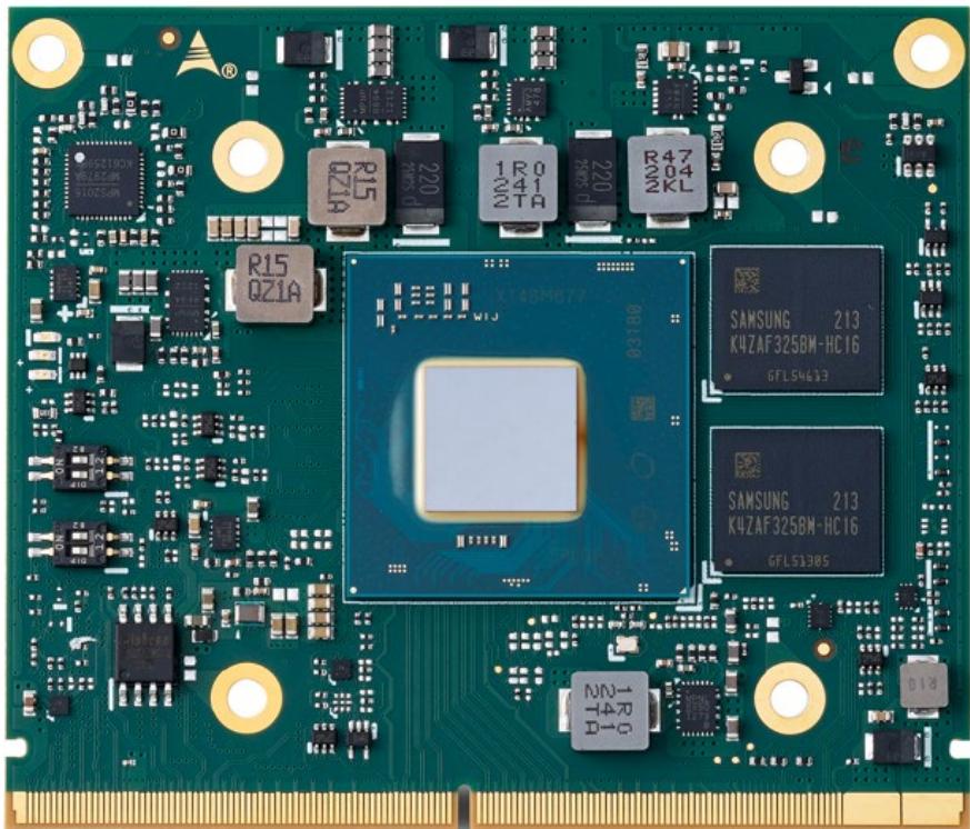
The MXM-AXe is an MXM 3.1 Type A-compliant module featuring Intel® Arc™ GPU (formerly “Alchemist”). It offers up to 8 Xe HPG, 8 Ray Tracing cores, and 128 Execution Units, along with 4GB GDDR6 at maximum bandwidth of 112 GB/s. Configurable up to 50W TGP and supporting PCIe Gen4 x8 lane connections make it well suit for various graphics-demanding applications, including medical ultrasound, gaming, media streaming, transportation, test and measurement, data analysis, defense, and more.
Graphics outputs include up to four simultaneous displays at DP 2.0 or HDMI 2.0. For graphics decoding and encoding, the MXM-AXe features DX12 Ultimate/DX12, Vulkan1.1, OpenCL 3.0, OpenGL 4.6 support AV1/VC/VC1/MPEG2/HEVC/H.265/VP9/JPEG HW decode and HEVC/AVC/MPEG2/VP9 HW encode.
By leveraging the well-established Intel graphics ecosystems, such as Intel OpenVINO for AI, Intel oneAPI (Media SDK inside) management tools, that edge developers have enjoyed and relied on for years, the MXM-AXe allows you to migrate from integrated to discrete graphics, and up to scale, smoothly and effortlessly.
# 2. Specifications
# 2.1. Core System
# GPU
Intel® $\mathsf { A r C } ^ { \mathsf { T M } }$ GPU Mobile (formerly codenamed “Alchemist”)
• Intel® Arc™ A370M 8 Xe cores, 8 Ray Tracing units, 128 Matrix Engines, 128 Vector Engines, 35W (configurable to 50W TGP)
• Intel® Arc™ A350M 6 Xe cores, 6 Ray Tracing units, 96 Matrix Engines, 96 Vector Engines, 25W (configurable to 35W TGP)
# Memory
GDDR6 4GB, 112 GB/s bandwidth, 64-bit interface width
# 2.2. Display Output
4 independent display outputs in varied combinations (4x 4K or 2x 8K, TBC)
DP 2.0, up to 5K@120Hz or 8K@60Hz
• HDMI 2.0, up to 4K@60Hz (specific VBIOS settings and switch setting on module required; also dependent on carrier board design)
# 2.3. Hardware Acceleration
• AV1, VC/VC1/MPEG2/HEVC/VP9/JPEG hardware decoding
HEVC/AVC/MPEG2/VP9/JPEG hardware encodeing
Ray tracing units and AI engines
# 2.4. Application Programming Interface — API
DirectX 12 Ultimate, DirectX 12
Vulkan 1.1
• OpenCL 3.0, OpenGL 4.6
# 2.5. Operation System
Microsoft Windows 11 / 10, Linux
# 2.6. Debug
MIPI20 on-board debug connector (additional specific fixture and cable required)
# 2.7. Mechanical and Environmental
Form Factor and Specification
MXM 3.1 Type A: 82mm x 70mm
Operating Temperature
| Standard | 0°C to 55°C |
| Industrial (TBC) | -20°C to 70°C |
| Storage: -40°C to 85°C |
| Storage: -40°C to 85°C |
Humidity
5-90% RH operating, non-condensing
5-95% RH storage (and operating with conformal coating)
HALT tested
Thermal Stress, and Thermal Shock
# 3. Block Diagram
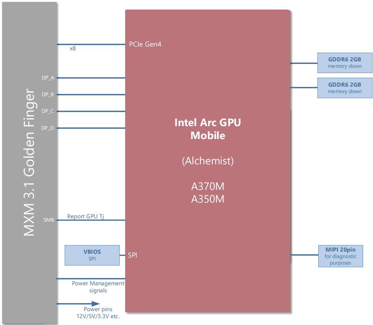
Figure 1 – Module function diagram
# 4. Pinout and Signal Descriptions
The table below is a comprehensible list of all signal pins supported as defined by MXM version 3.1 specification. Signals described in the specification but not supported on the MXM-AXe are marked with strike-through.
| Pin | Signal Name | | Pin | Signal Name | | Pin | Signal Name | | Pin | Signal Name |
| E1 | PWR_SRC | | E2 | PWR_SRC | | 55 | PEX_RX14# | | 56 | PEX_TX14 |
| E3 | GND | | E4 | GND | | 57 | PEX_RX14 | | 58 | GND |
| 1 | 5V | | 2 | PRSNT_R# | | 59 | GND | | 60 | PEX_TX13# |
| 3 | 5V | | 4 | WAKE# | | 61 | PEX_RX13# | | 62 | PEX_TX13 |
| 5 | 5V | | 6 | PWR_GOOD | | 63 | PEX_RX13 | | 64 | GND |
| 7 | 5V | | 8 | PWR_EN | | 65 | GND | | 66 | PEX_TX12# |
| 9 | 5V | | 10 | 27MHZ_REF | | 67 | PEX_RX12# | | 68 | PEX_TX12 |
| 11 | GND | | 12 | GND | | 69 | PEX_RX12 | | 70 | GND |
| 13 | GND | | 14 | LVDS_U_HPD | | 71 | GND | | 72 | PEX_TX11# |
| 15 | GND | | 16 | JTAG_TESTEN | | 73 | PEX_RX11# | | 74 | PEX_TX11 |
| 17 | GND | | 18 | PWR_LEVEL | | 75 | PEX_RX11 | | 76 | GND |
| 19 | PEX_STD_SW# | | 20 | TH_OVERT# | | 77 | GND | | 78 | PEX_TX10# |
| 21 | VGA_DISABLE# | | 22 | TH_ALERT# | | 79 | PEX_RX10# | | 80 | PEX_TX10 |
| 23 | PNL_PWR_EN | | 24 | TH_PWM | | 81 | PEX_RX10 | | 82 | GND |
| 25 | PNL_BL_EN | | 26 | GPIO0 | | 83 | GND | | 84 | PEX_TX9# |
| 27 | PNL_BL_PWM | | 28 | GPIO1 | | 85 | PEX_RX9# | | 86 | PEX_TX9 |
| 29 | HDMI_CEC | | 30 | GPIO2 | | 87 | PEX_RX9 | | 88 | GND |
| 31 | LVDS_L_HPD | | 32 | SMB_DAT | | 89 | GND | | 90 | PEX_TX8# |
| 33 | LVDS_DDC_DAT | | 34 | SMB_CLK | | 91 | PEX_RX8# | | 92 | PEX_TX8 |
| 35 | LVDS_DDC_CLK | | 36 | GND | | 93 | PEX_RX8 | | 94 | GND |
| 37 | GND | | 38 | OEM0 | | 95 | GND | | 96 | PEX_TX7# |
| 39 | OEM1 | | 40 | OEM2 | | 97 | PEX_RX7# | | 98 | PEX_TX7 |
| 41 | OEM3 | | 42 | OEM4 | | 99 | PEX_RX7 | | 100 | GND |
| 43 | OEM5 | | 44 | OEM6 | | 101 | GND | | 102 | PEX_TX6# |
| 45 | OEM7 | | 46 | GND | | 103 | PEX_RX6# | | 104 | PEX_TX6 |
| 47 | GND | | 48 | PEX_TX15# | | 105 | PEX_RX6 | | 106 | GND |
| 49 | PEX_RX15# | | 50 | PEX_TX15 | | 107 | GND | | 108 | PEX_TX5# |
| 51 | PEX_RX15 | | 52 | GND | | 109 | PEX_RX5# | | 110 | PEX_TX5 |
| 53 | GND | | 54 | PEX_TX14# | | 111 | PEX_RX5 | | 112 | GND |
| 113 | GND | | 114 | PEX_TX4# | | 183 | LVDS_UTX2 | | 184 | LVDS_LTX3 |
| 115 | PEX_RX4# | | 116 | PEX_TX4 | | 185 | GND | | 186 | GND |
| 117 | PEX_RX4 | | 118 | GND | | 187 | LVDS_UTX1# | | 188 | LVDS_LTX2# |
| 119 | GND | | 120 | PEX_TX3# | | 189 | LVDS_UTX1 | | 190 | LVDS_LTX2 |
| 121 | PEX_RX3# | | 122 | PEX_TX3 | | 191 | GND | | 192 | GND |
| 123 | PEX_RX3 | | 124 | GND | | 193 | LVDS_UTX0# | | 194 | LVDS_LTX1# |
| 125 | GND | | 126 | KEY | | 195 | LVDS_UTX0 | | 196 | LVDS_LTX1 |
| 127 | KEY | | 128 | KEY | | 197 | GND | | 198 | GND |
| 129 | KEY | | 130 | KEY | | 199 | DP_C_L0# | | 200 | LVDS_LTX0# |
| 131 | KEY | | 132 | KEY | | 201 | DP_C_L0 | | 202 | LVDS_LTX0 |
| 133 | GND | | 134 | GND | | 203 | GND | | 204 | GND |
| 135 | PEX_RX2# | | 136 | PEX_TX2# | | 205 | DP_C_L1# | | 206 | DP_D_L0# |
| 137 | PEX_RX2 | | 138 | PEX_TX2 | | 207 | DP_C_L1 | | 208 | DP_D_L0 |
| 139 | GND | | 140 | GND | | 215 | GND | | 216 | GND |
| 141 | PEX_RX1# | | 142 | PEX_TX1# | | 217 | DP_C_L3# | | 218 | DP_D_L2# |
| 143 | PEX_RX1 | | 144 | PEX_TX1 | | 219 | DP_C_L3 | | 220 | DP_D_L2 |
| 145 | GND | | 146 | GND | | 221 | GND | | 222 | GND |
| 147 | PEX_RX0# | | 148 | PEX_TX0# | | 223 | DP_C_AUX# | | 224 | DP_D_L3# |
| 149 | PEX_RX0 | | 150 | PEX_TX0 | | 225 | DP_C_AUX | | 226 | DP_D_L3 |
| 151 | GND | | 152 | GND | | 227 | RSVD | | 228 | GND |
| 153 | PEX_REFCLK# | | 154 | PEX_CLK_REQ# | | 229 | RSVD | | 230 | DP_D_AUX# |
| 155 | PEX_REFCLK | | 156 | PEX_RST# | | 231 | RSVD | | 232 | DP_D_AUX |
| 157 | GND | | 158 | VGA_DDC_DAT | | 233 | RSVD | | 234 | DP_C_HPD |
| 159 | JTAG_TDO | | 160 | VGA_DDC_CLK | | 235 | RSVD | | 236 | DP_D_HPD |
| 161 | JTAG_TDI | | 162 | VGA_VSYNC | | 237 | RSVD | | 238 | RSVD |
| 163 | JTAG_TCLK | | 164 | VGA_HSYNC | | 239 | RSVD | | 240 | 3V3 |
| 165 | JTAK_TMS | | 166 | GND | | 241 | RSVD | | 242 | 3V3 |
| 167 | JTAG_TRST# | | 168 | VGA_RED | | 243 | RSVD | | 244 | GND |
| 169 | JTAG_UCLK# | | 170 | VGA_GREEN | | 245 | RSVD | | 246 | DP_B_L0# |
| 171 | JTAG_UCLK | | 172 | VGA_BLUE | | 247 | RSVD | | 248 | DP_B_L0 |
| 173 | GND | | 174 | GND | | 249 | RSVD | | 250 | GND |
| 175 | LVDS_UTX3# | | 176 | LVDS_LCLK# | | 251 | GND | | 252 | DP_B_L1# |
| 177 | LVDS_UTX3 | | 178 | LVDS_LCLK | | 253 | DP_A_L0# | | 254 | DP_B_L1 |
| 179 | GND | | 180 | GND | | 255 | DP_A_L0 | | 256 | GND |
| 181 | LVDS_UTX2# | | 182 | LVDS_LTX3# | | 257 | GND | | 258 | DP_B_L2# |
| 259 | DP_A_L1# | | 260 | DP_B_L2 | | 269 | GND | | 270 | DP_B_AUX# |
| 261 | DP_A_L1 | | 262 | GND | | 271 | DP_A_L3# | | 272 | DP_B_AUX |
| 263 | GND | | 264 | DP_B_L3# | | 273 | DP_A_L3 | | 274 | DP_B_HPD |
| 265 | DP_A_L2# | | 266 | DP_B_L3 | | 275 | GND | | 276 | DP_A_HPD |
| 267 | DP_A_L2 | | 268 | GND | | 277 | DP_A_AUX# | | 278 | 3V3 |
# 5. Additional Features
This chapter describes connectors, switches, and additional items located on the module and not necessarily included in the MXM standard specification. The locations of these items are as below:
# 5.1. Module Feature Locations
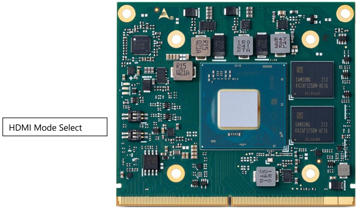
Figure 2 – Module feature locations (top side)
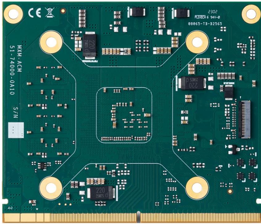
MIPI20 Debug Connector (for debug purposes only)
Figure 3 – Module feature locations (bottom side)
# 5.2. HDMI Mode Select
The HDMI Mode Select Switch allows you to configure the display outputs to be HDMI signals. A specific VBIOS setting and level shift for HDMI usage on carrier board are also required
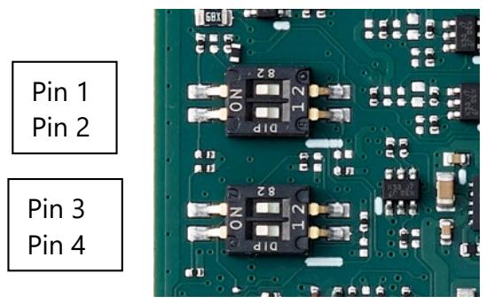
| Mode | Pin 1(DP_A Port) | Pin 2(DP_B Port) | Pin 3(DP_C Port) | Pin 4(DP_D Port) |
| DP (default) | On | On | On | On |
| HDMI | Off | Off | Off | Off |
# 5.3. MIPI20 Debug Connector
This connector is particular useful during bring up phase. It will require additional MIPI20 to MIPI60 cable and a dedicated debug card with specific SW tool. This is only for ADLINK internal debug usage.
# 6. Mechanical
All dimensions are shown in millimetres, with a tolerance of ± 0.25mm unless otherwise noted.
# 6.1. Module Dimensions – Top View
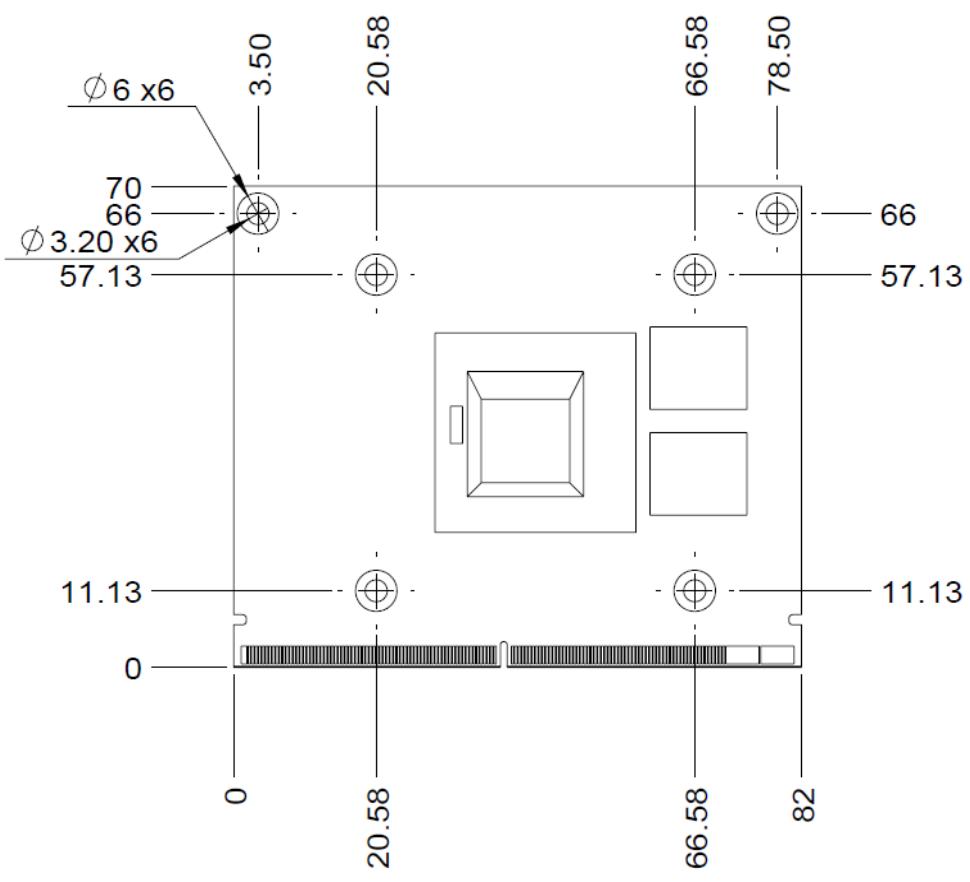
Figure 4 – Module dimensions (top view)
# 6.2. Module Dimensions – Bottom View
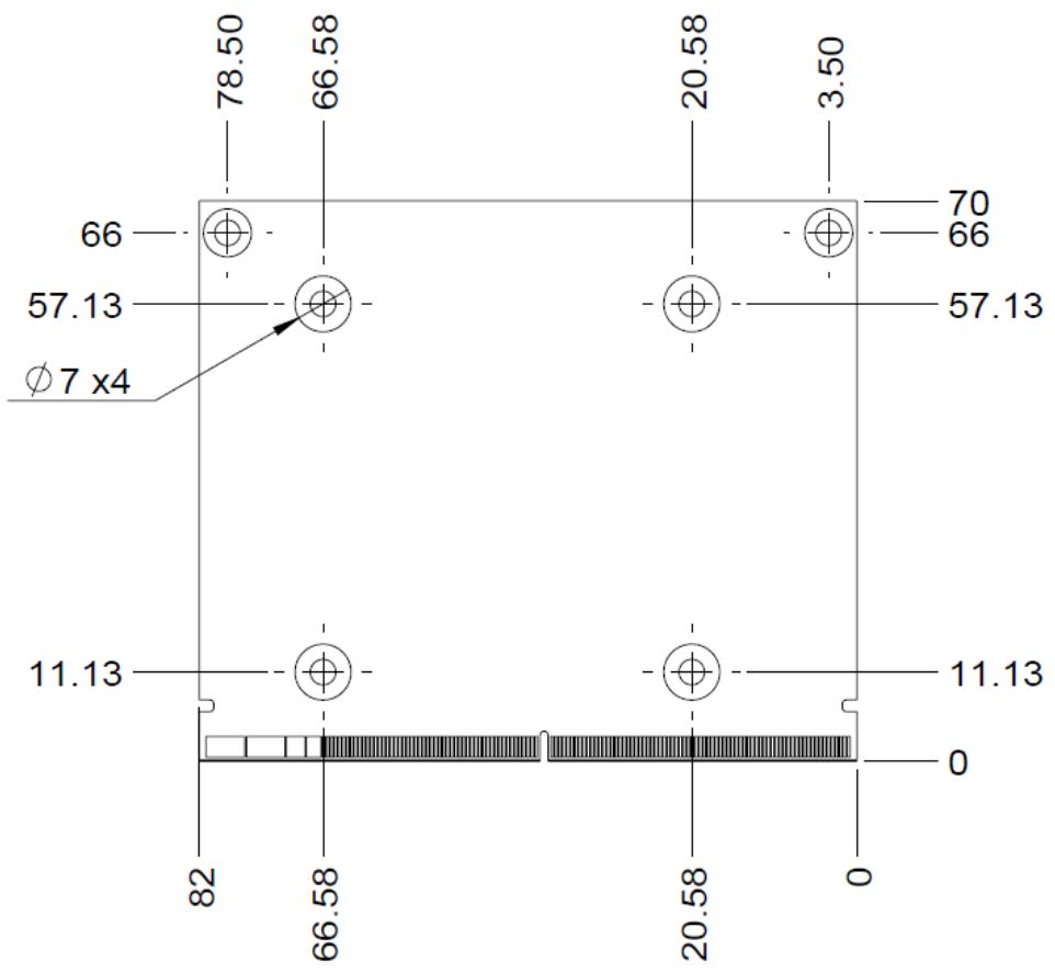
Figure 5 – Module dimensions (bottom view)
# 6.3. Module Dimensions – Side View
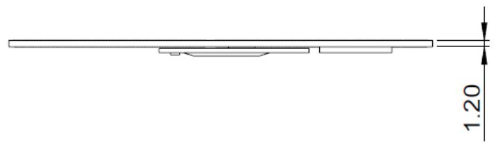
Figure 6 – Module dimensions (side view)
# 6.4. GPU Height
The tolerance of GPU or CPU height should be taken into consideration for the design of your thermal solution. A preliminary illustration is shown below. Please contact your local ADLINK representative for details.
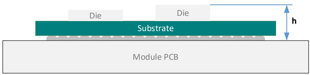
| Typical | Tolerance |
| h | 1.776 mm | ±0.109 mm |
# 7. Thermal Solution
# 7.1. Heatsink with Fan: THSF
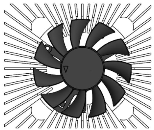
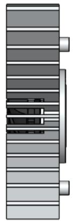
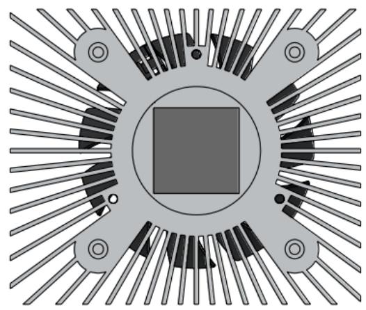
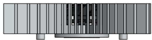
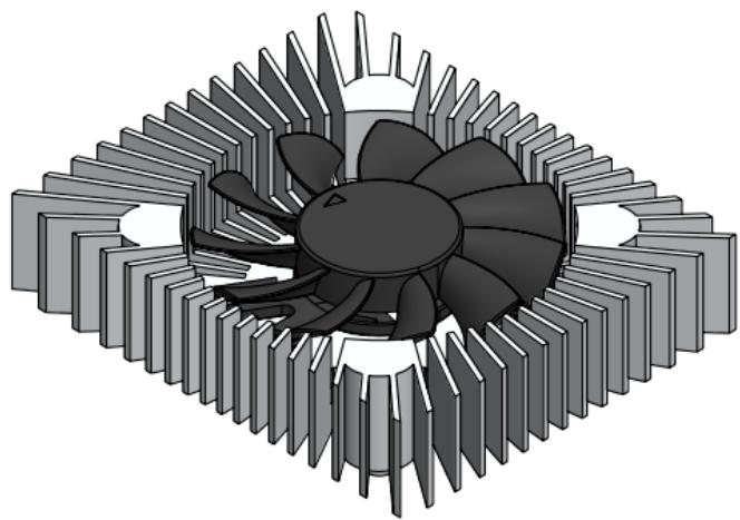
Figure 7 – Heatsink with Fan (THSF)
[🔗 Link to the original document](.mxm-axe-manual-50m-74000-1000-10-230731/mxm-axe-manual-50m-74000-1000-10-230731.pdf)