NuDAM-6011/

NuDAM-6014D

NuDAM-6012/D

NuDAM-6017

NuDAM-6013/

NuDAM-6018

Analog Input Modules

User's Guide

©Copyright 1996\~2001 ADLINK Technology Inc. All Rights Reserved.

Manual Rev. 5.15: October 2, 2001

The information in this document is subject to change without prior notice in order to improve reliability, design and function and does not represent a commitment on the part of the manufacturer.

In no event will the manufacturer be liable for direct, indirect, special, incidental, or consequential damages arising out of the use or inability to use the product or documentation, even if advised of the possibility of such damages.

This document contains proprietary information protected by copyright. All rights are reserved. No part of this manual may be reproduced by any mechanical, electronic, or other means in any form without prior written permission of the manufacturer.

# Trademarks

NuDAM is registered trademarks of ADLINK Technology Inc.,

Other product names mentioned herein are used for identification purposes only and may be trademarks and/or registered trademarks of their respective companies.

# Getting service from ADLINK

◆ Customer Satisfaction is always the most important thing for ADLINK Tech Inc. If you need any help or service, please contact us and get it.

<table><tr><td colspan="4">ADLINK Technology Inc.</td></tr><tr><td>Web Site</td><td colspan="3">http://www.adlink.com.tw</td></tr><tr><td>Sales &amp; Service</td><td colspan="3">service@adlink.com.tw</td></tr><tr><td>Technical</td><td>NuDAQ</td><td colspan="2">nudaq@adlink.com.tw</td></tr><tr><td>Support</td><td>NuDAM</td><td colspan="2">nudam@adlink.com.tw</td></tr><tr><td></td><td>NuIPC</td><td colspan="2">nuipc@adlink.com.tw</td></tr><tr><td></td><td>NuPRO</td><td colspan="2">nupro@adlink.com.tw</td></tr><tr><td></td><td>Software</td><td colspan="2">sw@adlink.com.tw</td></tr><tr><td>TEL</td><td>+886-2-82265877</td><td>FAX</td><td>+886-2-82265717</td></tr><tr><td>Address</td><td colspan="3">9F, No. 166, Jian Yi Road, Chungho City, Taipei, 235 Taiwan, R.O.C.</td></tr></table>

Please inform or FAX us of your detailed information for a prompt, satisfactory and constant service.

<table><tr><td colspan="4">Detailed Company Information</td></tr><tr><td>Company/Organization</td><td colspan="3"></td></tr><tr><td>Contact Person</td><td colspan="3"></td></tr><tr><td>E-mail Address</td><td colspan="3"></td></tr><tr><td>Address</td><td colspan="3"></td></tr><tr><td>Country</td><td colspan="3"></td></tr><tr><td>TEL</td><td></td><td>FAX</td><td></td></tr><tr><td>Web Site</td><td colspan="3"></td></tr><tr><td colspan="4">Questions</td></tr><tr><td>Product Model</td><td colspan="3"></td></tr><tr><td>Environment to Use</td><td colspan="3">☐O ____☐Computer ____☐M/B: ☐CPU:☐Chipset: ☐BIOS:☐Video Card:☐Network Interface Card:☐Other:</td></tr><tr><td>Challenge Description</td><td colspan="3"></td></tr><tr><td>Suggestions for ADLINK</td><td colspan="3"></td></tr></table>

# Table of Contents

# Chapter 1 Introduction....1

1.1 About the NuDAM Analog Input Modules....1
1.2 Overview of NuDAM-6011/D....1

What is NuDAM-6011/D ?......1
Features of NuDAM-6011/D 2
Specifications of NuDAM-6011/D 2
Pin Definitions of ND-6011/D 4
Functional Block Diagram of ND-6011/D 4
A Look at ND-6011/D & Pin Assignment....5

1.3 Overview of NuDAM-6012/D 6

What is NuDAM-6012/D?......6
Features of NuDAM-6012/D....6
Specifications of NuDAM-6012/D....6
Pin Definitions of ND-6012/D 8
Functional Block Diagram of ND-6012/D 8
A Look at ND-6012/D & Pin Assignment....9

1.4 Overview of NuDAM-6013 10

What is NuDAM-6013 ? 10
Features of NuDAM-6013 10
Specifications of NuDAM-6013 10
Pin Definitions of ND-6013.... 11
Functional Block Diagram of ND-6013.... 11
A Look at ND-6013 & Pin Assignment 12

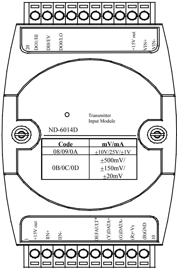
1.5 Overview of NuDAM-6014D....13

What is NuDAM-6014D ? 13
Features of NuDAM-6014D 13
Specifications of NuDAM-6014D.... 13
Pin Definitions of ND-6014D 15
Functional Block Diagram of ND-6014D 15
A Look at ND-6014D & Pin Assignment.... 16

1.6 Overview of NuDAM-6017 17

What is NuDAM-6017 ? 17
Features of NuDAM-6017 17
Specifications of NuDAM-6017 17
Pin Definitions of ND-6017.... 18
Functional Block Diagram of ND-6017 18
A Look at ND-6017 & Pin Assignment 19

1.7 Overview of NuDAM-6018 20

What is NuDAM-6018 ? 20

Features of NuDAM-6018 20

Specifications of NuDAM-6018 20

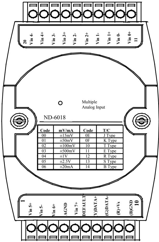
Pin Definitions of ND-6018 21

Functional Block Diagram of ND-6018 21

A Look at ND-6018 & Pin Assignment 22

# Chapter 2 Initialization & Installation....23

2.1 Software Installation....23

2.2 Initializing a Brand-New Module 23

Objective of Initializing a Brand-New NuDAM 23

Default State 24

Initialization Equipments 24

Initialization Procedure.... 24

Initialization Wiring 25

2.3 Install a New NuDAM to a Existing Network....25

Equipments for Install a New Module 25

Installing Procedures.... 25

2.4 Application Wiring for NuDAM-601X....26

Differential Voltage Input 26

Single Ended Voltage Input 26

Current Measurement 26

Digital Input Connect with TTL Signal 27

Digital Input Used as an Event Counter 27

Digital Output Connect with Power Loading 27

RTD Input (NuDAM-6013) 28

Application Wiring for NuDAM-6014D 29

Transmitter wiring for NuDAM-6014D 30

# Chapter 3 Command Set....31

3.1 Command and Response 31

Introduction 31

Document Conventions.... 31

Format of NuDAM Commands 32

Response of NuDAM Commands 33

3.2 Summary of Command Set....33

3.3 Set Configuration 37

3.4 Read Configuration 41

3.5 Read Module Name 42

3.6 Read Firmware Version 43

3.7 Software Reset......44

3.8 Synchronized Sampling 45

3.9 Read Synchronized Data 46

3.10 Read Analog Data....47

3.11 Span Calibration 48

3.12 Span Calibration to each Channel 49

3.13 Offset Calibration 50
3.14 Offset Calibration to each Channel....51
3.15 Read Analog Data From Channel N 52
3.16 Read All Analog Data Channel 53
3.17 Enable/Disable channels for Multiplexing 54
3.18 Read Channel Status....55
3.19 Read CJC Status 56
3.20 Enable/Disable CJC 57
3.21 Read enable/disable CJC Status 58
3.22 Read Source High/Low Values for Linear Mapping......59
3.23 Read Target High/Low Values for Linear Mapping......60
3.24 Write Source High/Low Values for Linear Mapping ......61
3.25 Write Target High/Low Values for Linear Mapping 62
3.26 Enable/Disable Linear Mapping 63
3.27 Read enable/Disable Linear Mapping Status 64
3.28 CJC Offset Calibration 65
3.29 Clear Latched Alarm 66
3.30 Clear Event Counter 67
3.31 Disable Alarm....68
3.32 Read Digital I/O and Alarm Status 69
3.33 Set Digital Output....71
3.34 Enable Alarm....72
3.35 Set High Alarm....73
3.36 Set Low Alarm....74
3.37 Read Event Counter 75
3.38 Read High Alarm Limit 76
3.39 Read Low Alarm Limit 77
3.40 Read Leading Code Setting....78
3.41 Change Leading Code Setting....80
3.42 Set Host Watchdog Timer & Safety Value......82
3.43 Read Host Watchdog Timer & Safety Value....84
3.44 Host is OK....85

# Chapter 4 Data Format and Input Range 86

4.1 Data Format of Analog Input Modules 86

Engineering Units 86

Percent of FSR (Full Scale Range) 87

Two's Complement Hexadecimal.... 88

Ohm 89

4.2 Analog Input Range 90

# Chapter 5 Calibration ...... 93

# 5.1 How to Calibrate the Analog Input Modules ? .....93

What do you need to do calibration ?...... 93

Calibration Procedure for ND-6011/D, 6012/D, 6014D, 6017 ..... 93

Calibration Procedure for ND-6013 (F/W version A3.05) 94

Calibration Procedure for ND-6013 Firmware Rev C4.60 94

Calibration Procedure for ND-6018 Firmware Rev B1.10 95

Calibration Procedure for ND-6018 Firmware Rev E1.00 and e1.00 95

CJC Calibration Procedure 96

Analog Input Module's Calibration Voltages....97

# Product Warranty/Service....99

![1](.nd-6013-manual-2/cdbf72012b303978d0667d786802b94335b62488652e220b092e5bf7d3d7c4d6.jpg)

# Introduction

# 1.1 About the NuDAM Analog Input Modules

The NuDAM provides a series of analog input modules which can sense the analog signal or to control the remote devices. The basic features of each module are shown here.

• NuDAM-6011/D: multi-functions high gain analog input module
• NuDAM-6012/D: multi-functions analog input module
• NuDAM-6013: 3 channels RTD input module
- NuDAM-6014D:Analog (Transmitter) input module with LED display
• NuDAM-6017: 8 channels analog input module
• NuDAM-6018: 8 channels thermocouple input module

The models with an extended D have the same command set and specification as without D, except the D version has a 5 1/2 LED Display.

# 1.2 Overview of NuDAM-6011/D

# What is NuDAM-6011/D ?

NuDAM-6011/D is a multi-functions analog input module with cold junction compensation (CJC). The maximum input voltage range of analog input channel is $\pm2.5V$ . The high gain feature allows very small full range of $\pm15mV$ . To measure temperature by directly connect the thermocouple is possible because of using the CJC inside and the high gain feature. The voltage range of the ADC can be set according to different types of thermocouple. The ADC can be calibrated by programming without handy adjustment. This features insure the best performance under different environment.

The module provides the analog signal monitor or the alarm function. The high and low bound of the alarm limit is programmable. The alarm status can be sent to digital output channels if this function is ON. The supervisor of a factory can 'see' or 'hear' the alarm if the digital output channel control a real alarm device. The two digital output channels can be set for general-purpose use if the alarm is disabled.

For example, connecting relay devices to DO channels, the NuDAM-6011/D can be used to control the high power devices.

The module provides another one digital input channel. This can be used for general purpose such as monitor digital signal, or be used as input of the event counter.

# Features of NuDAM-6011/D

• 1 analog input channel with differential input
• Programmable voltage range with high gain amplifier
• On board CJC for temperature measurement
- 5000 Vrms isolation voltage for AD channel (2500 Vrms for NuDAM-6011/D)
• 2 digital output channels of open collector type
• Alarm function with high / low alarm output
• 1 digital input channel / event counter
• Programmable host watchdog timer for host failure protection
• Internal watchdog timer for device failure protection
• Easy programming by software
• Easy installation and wiring
• 5 1/2 digital LED Display (NuDAM-6011/D)

# Specifications of NuDAM-6011/D

# Interface

• Interface: RS-485, 2 wires
- Speed (bps): 1200, 2400, 4800, 9600, 19.2K, 38.4K, 115.2K (115.2K only for firmware reversion above A4.00)

# ✨ Analog Input

• Input type: Differential input
• Resolution: 16 bits
• Unit Conversion: Thermocouple, mV, V, or mA
• Thermocouple Type: J, K, T, E, R, S, B, N, C

J: 0°C\~760°C

T: $-100^{\circ}C \sim 400^{\circ}C$

R: 500°C\~1750°C

B: $500^{\circ}$ C\~ $1800^{\circ}$ C

K: $0^{\circ}$ C\~1370°C $^{(1)}$

E: $0^{\circ}$ C\~ $1000^{\circ}$ C

S: 500°C\~1750°C

N: -270°C\~1300°C

C: 0°C\~2320°C

• Voltage Range: Programmable 6 levels ±2.5V, ±1V, ±500mV, ±100mV, ±50mV, ±15mV
• Current Measurement: ±20mA (with external 125Ω resistor)
• Accuracy: ±0.4%

Note (1): F/W version above A4.60 support K-type for 0\~1370°C. Lower version supports K-type for 0\~1000°C.

# Digital Output

• Channel numbers: 2
• Output characteristic: open collector transistor
• Maximum current sink: 50mA
• Max. power dissipation: 300mW

# Digital Input

• Channel numbers: 1
• Logical level 0: +1V maximum
• Logical level 1: +2.0V\~ +30V
• Pull up resistor: 10KΩ
• Maximum current: 0.5mA

# ✨ Watchdog Function

• Module internal watchdog timer: 150 ms
• Power failure threshold: 4.65 V
• Safety value: 2 digital output channels
• Host programmable watchdog: 100 ms \~ 25.500 sec

# Power

• Power supply: +10V to +30V
• Current consumption: 0.76W(1.68W for NuDAM-6011/D)

Pin Definitions of ND-6011/D

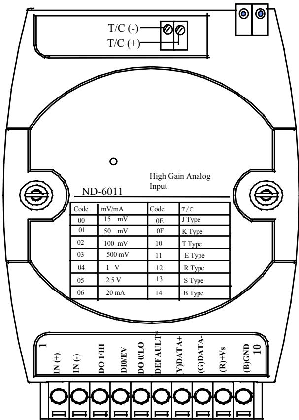
<table><tr><td>Pin #</td><td>Signal Name</td><td>Description</td></tr><tr><td>1</td><td>IN+</td><td>Analog Input Positive Terminal</td></tr><tr><td>2</td><td>IN-</td><td>Analog Input Negative Terminal</td></tr><tr><td>3</td><td>DO 1/ HI</td><td>Digital Output Channel 1 or High alarm status output</td></tr><tr><td>4</td><td>DI 0 / EV</td><td>Digital Input Channel 0 or event counter input</td></tr><tr><td>5</td><td>DO 0 / LO</td><td>Digital Output Channel 0 or Low alarm output</td></tr><tr><td>6</td><td>DEFAULT*</td><td>Initial state setting</td></tr><tr><td>7</td><td>(Y) DATA+</td><td>RS-485 series signal, positive</td></tr><tr><td>8</td><td>(G) DATA-</td><td>RS-485 series signal, negative</td></tr><tr><td>9</td><td>(R) +Vs</td><td>Power supply, +10V~+30V</td></tr><tr><td>10</td><td>(B) GND</td><td>Ground</td></tr><tr><td>11</td><td>TC(+)</td><td>Thermocouple Input positive Terminal</td></tr><tr><td>12</td><td>TC(-)</td><td>Thermocouple Input negative Terminal</td></tr></table>

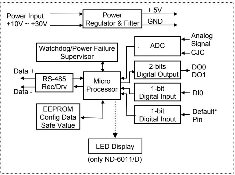
Functional Block Diagram of ND-6011/D

![Based on the provided flowchart, here is an accurate and concise description of the blocks and their connections:\n\n**Labeled Blocks:**\n*   Power Input +10V ~ +30V\n*   Power Regulator & Filter\n*   + 5V\n*   GND\n*   Watchdog/Power Failure Supervisor\n*   Analog Signal\n*   CJC\n*   ADC\n*   2-bits Digital Output\n*   DO0\n*   DO1\n*   Data +\n*   Data -\n*   RS-485 Rec/Drv\n*   Micro Processor\n*   1-bit Digital Input (appears as two separate blocks)\n*   DI0\n*   Default* Pin\n*   EEPROM Config Data Safe Value\n*   LED Display (only ND-6011/D)\n\n**Connections:**\n*   **Power Section:** **Power Input +10V ~ +30V** connects to **Power Regulator & Filter**, which outputs to **+ 5V** and **GND**.\n*   **Micro Processor Interconnections:**\n    *   **Watchdog/Power Failure Supervisor** connects bidirectionally to the **Micro Processor**.\n    *   **EEPROM Config Data Safe Value** connects bidirectionally to the **Micro Processor**.\n    *   **RS-485 Rec/Drv** connects bidirectionally to the **Micro Processor**.\n        *   **Data +** and **Data -** connect bidirectionally to **RS-485 Rec/Drv**.\n    *   **ADC** connects bidirectionally to the **Micro Processor**.\n        *   **Analog Signal** and **CJC** connect to the **ADC**.\n    *   **2-bits Digital Output** receives a signal from the **Micro Processor** and outputs to **DO0** and **DO1**.\n    *   **1-bit Digital Input** (top block) connects bidirectionally to the **Micro Processor** and receives input from **DI0**.\n    *   **1-bit Digital Input** (bottom block) connects bidirectionally to the **Micro Processor** and receives input from **Default* Pin**.\n    *   **LED Display (only ND-6011/D)** receives a signal (indicated by a dotted arrow) from the **Micro Processor**.](.nd-6013-manual-2/aba58d9f169cce4e6540e6d2db760bad51ce71e9048dde34e34fe5724282f2ae.jpg)

A Look at ND-6011/D & Pin Assignment
![T/C (-)\nT/C (+)\nHigh Gain Analog\nInput\nND-6011\nCode	mV/mA	Code	T/C\n00	15 mV	0E	J Type\n01	50 mV	0F	K Type\n02	100 mV	10	T Type\n03	500 mV	11	E Type\n04	1 V	12	R Type\n05	2.5 V	13	S Type\n06	20 mA	14	B Type\n1\nIN (+)	N IN (-)	DO 1/HH	DIO/EV	DO 0/LO	DEFAULT	Y)+DATA-\n(G)DATA-\n(R)+Vs	(B)GND\n10](.nd-6013-manual-2/37b386e381128610fbdbf8e7b7f22c59787507197f5cfa561e92901822a6cee2.jpg)

# 1.3 Overview of NuDAM-6012/D

# What is NuDAM-6012/D?

NuDAM-6012/D is a multi-functions analog input module. The programmable input voltage range of analog input channel is from $\pm10V$ maximum to $\pm150mV$ minimum.

The module also provides the alarm function and the event counter just like NuDAM-6011/D. In fact, the NuDAM-6012/D provides almost all functions that NuDAM-6011/D has except the CJC and temperature measurement function.

# Features of NuDAM-6012/D

• 1 analog input channel with differential input
• Programmable voltage range
- 5000 Vrms isolation voltage for AD channel (2500 Vrms for ND-6012/D)
• 2 digital output channels of open collector type
• Alarm function with high / low alarm output
• 1 digital input channel / event counter
• Programmable host watchdog timer for host failure protection
• Internal watchdog timer for device failure protection
• Easy programming by software
• Easy installation and wiring
• 51/2 digital LED display (NuDAM-6012/D)

# Specifications of NuDAM-6012/D

# Interface

• Interface: RS-485, 2 wires
- Speed (bps): 1200, 2400, 4800, 9600, 19.2K, 38.4K, 115.2K (115.2K only for firmware reversion above A4.00)

# ✨ Analog Input

• Input type: Differential input
• Resolution: 16 bits
• Unit Conversion: mV, V, or mA
• Voltage Range: Programmable 5 levels ±10V, ±5V, ±1V, ±500mV, ±150mV
• Current Measurement: ±20mA (with external 125Ω resistor)
• Accuracy: ±0.05%
• Isolation Voltage: 5000 Vrms(2500 Vrms for NuDAM-6012/D)

# Digital Output

• Channel numbers: 2
• Output characteristic: open collector transistor
• Maximum current sink: 50mA
• Max. power dissipation: 300mW

# Digital Input

• Channel numbers: 1
• Logical level 0: +1V maximum
• Logical level 1: +2.0V\~30V
• Pull up resistor: 10KΩ
• Maximum current: 0.5mA

# ✨ Watchdog Function

• Module internal watchdog timer: 150 ms
• Power failure threshold: 4.65 V
- Host programmable watchdog: 100 ms \~ 25.500 sec

# Power

• Power supply: +10V to +30V
• Current consumption: 1.1 W(2.0W for NuDAM-6012/D)

Pin Definitions of ND-6012/D

<table><tr><td>Pin #</td><td>Signal Name</td><td>Description</td></tr><tr><td>1</td><td>IN+</td><td>Analog Input Positive Terminal</td></tr><tr><td>2</td><td>IN-</td><td>Analog Input Negative Terminal</td></tr><tr><td>3</td><td>DO 1/ HI</td><td>Digital Output Channel 1 or High alarm status output</td></tr><tr><td>4</td><td>DI 0 / EV</td><td>Digital Input Channel 0 or event counter input</td></tr><tr><td>5</td><td>DO 0 / LO</td><td>Digital Output Channel 0 or Low alarm output</td></tr><tr><td>6</td><td>DEFAULT*</td><td>Initial state setting</td></tr><tr><td>7</td><td>(Y) DATA+</td><td>RS-485 series signal, positive</td></tr><tr><td>8</td><td>(G) DATA-</td><td>RS-485 series signal, negative</td></tr><tr><td>9</td><td>(R) +Vs</td><td>Power supply, +10V~+30V</td></tr><tr><td>10</td><td>(B) GND</td><td>Ground</td></tr></table>

Functional Block Diagram of ND-6012/D
![The diagram illustrates a system architecture centered around a microprocessor. Here are the labeled blocks and their connections:\n\n**Power Section**\n*   **Power Input +10V ~ +30V**: Two arrows point from this label into the 'Power Regulator & Filter' block.\n*   **Power Regulator & Filter**: Outputs are shown to the right: one arrow points up to '+ 5V' and another points down to 'GND'.\n\n**Central Processing Unit**\n*   **Micro Processor**: This block is in the center and connects to all other major blocks.\n    *   **Watchdog/Power Failure Supervisor**: Connected via a double-headed arrow (bidirectional).\n    *   **RS-485 Rec/Drv**: Connected via a double-headed arrow (bidirectional).\n        *   **Data +** and **Data -**: Two arrows point left from 'RS-485 Rec/Drv'.\n    *   **EEPROM Config Data Safe Value**: Connected via an arrow pointing from the Micro Processor to the EEPROM block.\n    *   **ADC**: Connected via a double-headed arrow (bidirectional).\n        *   **Analog Signal**: An arrow points right from the ADC block.\n    *   **2-bits Digital Output**: Connected via a double-headed arrow (bidirectional).\n        *   **DO0 DO1**: Two arrows point right from this block.\n    *   **1-bit Digital Input** (top): Connected via a double-headed arrow (bidirectional).\n        *   **nIn**: An arrow points left into this block.\n    *   **1-bit Digital Input** (bottom): Connected via a double-headed arrow (bidirectional).\n        *   **Default* Pin**: An arrow points left into this block.\n\n**Display**\n*   **LED Display (only ND-6012/D)**: Connected to the Micro Processor via a dotted arrow pointing upwards.](.nd-6013-manual-2/1f7c4b2276f2b4901b5879ca286815c6db2ef531ca328c65876eea639a9274b4.jpg)

A Look at ND-6012/D & Pin Assignment
![20\n11\nHigh Gain Analog\nInput\nND-6012\nCode	mV/mA\n08	10V\n09	5 V\n0A	1 V\n0B	500 mV\n0C	150 mV\n0D	20 mA\n1\nIN (+)	IN (-)	DO 1/HI	DI0/EV	DO 0/LO	DEFAULT	Y)DATA+\n(G)DATA-\n(R)+Vs	(B)GND\n10](.nd-6013-manual-2/3b7642737083f26252e1aae3494c3a6cf9519bc2699708892b5bb2be9a193a13.jpg)

# 1.4 Overview of NuDAM-6013

# What is NuDAM-6013?

NuDAM-6013 is a RTD input module with 3 input channels. It supports 2, 3 or 4 wires RTD input device.

# Features of NuDAM-6013

• 3 RTD input channels
• 2, 3 or 4 wire RTD input support
• Programmable RTD input range
• Internal watchdog timer for device failure protection
• Easy programming by software
• Easy installation and wiring

Note $^{(2)}$ : for H/W version C1.2 or above and F/W version C4.6 or above.

# Specifications of NuDAM-6013

# Interface

• Interface: RS-485, 2 wires
- Speed (bps): 1200, 2400, 4800, 9600, 19.2K, 38.4K, 115.2K (115.2K only for firmware reversion above A4.00)

# RTD Input

• Input type: Pt or Ni input, 2, 3 or 4 wires
• Channels Numbers: 3
• Resolution: 16 bits
• Unit Conversion: °C or Ohm
- Temperature Range: Programmable 5 levels, ±100°C, 0\~100°C, 0\~200°C, 0\~600°C, 0\~60 Ohms $^{(3)}$
• Accuracy: ±0.1%

Note $^{(3)}$ : Supported on F/W version C4.5 or above.

# Power

• Power supply: +10V to +30V
• Current consumption: 0.65 W

# Pin Definitions of ND-6013

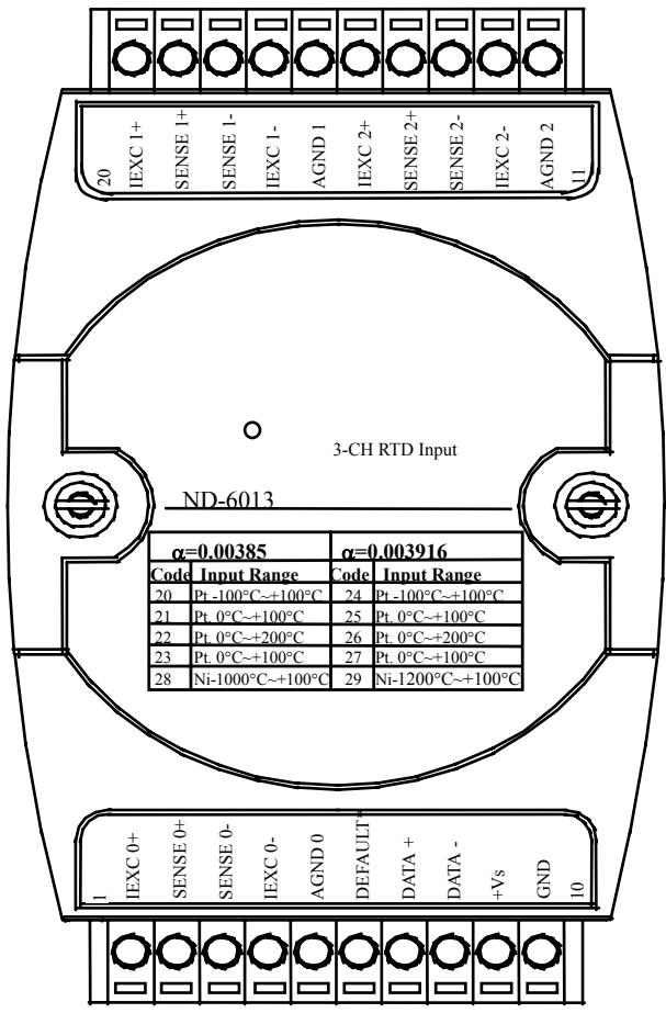
<table><tr><td>Pin #</td><td>Signal Name</td><td>Description</td></tr><tr><td>1</td><td>+IEXC0</td><td>Current source of CH0</td></tr><tr><td>2</td><td>+SENSE0</td><td>Differential positive input of CH0</td></tr><tr><td>3</td><td>-SENSE0</td><td>Differential negative input of CH0</td></tr><tr><td>4</td><td>-IEXC0</td><td>Current source of CH0</td></tr><tr><td>5</td><td>AGND0</td><td>Analog signal ground of CH0</td></tr><tr><td>6</td><td>DEFAULT*</td><td>Initial state setting</td></tr><tr><td>7</td><td>(Y) DATA+</td><td>RS-485 series signal, positive</td></tr><tr><td>8</td><td>(G) DATA-</td><td>RS-485 series signal, negative</td></tr><tr><td>9</td><td>(R) +Vs</td><td>Power supply, +10V~+30V</td></tr><tr><td>10</td><td>(B) GND</td><td>Ground</td></tr><tr><td>11</td><td>AGND2</td><td>Analog signal ground of CH2</td></tr><tr><td>12</td><td>-ISEC2</td><td>Current source of CH2</td></tr><tr><td>13</td><td>-SENSE2</td><td>Differential negative input of CH2</td></tr><tr><td>14</td><td>+SENSE2</td><td>Differential positive input of CH2</td></tr><tr><td>15</td><td>+IEXC2</td><td>Current source of CH2</td></tr><tr><td>16</td><td>AGND1</td><td>Analog signal ground of CH1</td></tr><tr><td>17</td><td>-ISEC1</td><td>Current source of CH1</td></tr><tr><td>18</td><td>-SENSE1</td><td>Differential negative input of CH1</td></tr><tr><td>19</td><td>+SENSE1</td><td>Differential positive input of CH1</td></tr><tr><td>20</td><td>+IEXC1</td><td>Current source of CH1</td></tr></table>

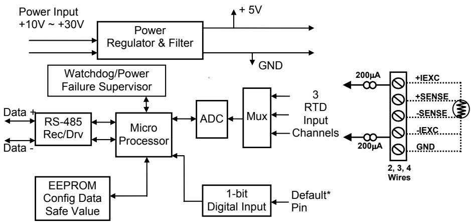
# Functional Block Diagram of ND-6013

![Based on the provided block diagram, here is the accurate description of the labeled blocks and their connections:\n\n**Power Section**\n*   **Power Input +10V ~ +30V** connects to **Power Regulator & Filter**.\n*   **Power Regulator & Filter** outputs to **+ 5V** and **GND**.\n\n**Central Processing Unit & Peripherals**\n*   **Micro Processor** is the central block.\n*   **Watchdog/Power Failure Supervisor** connects bidirectionally to the **Micro Processor**.\n*   **RS-485 Rec/Drv** connects bidirectionally to the **Micro Processor**.\n    *   **RS-485 Rec/Drv** connects bidirectionally to **Data +** and **Data -**.\n*   **EEPROM Config Data Safe Value** connects to the **Micro Processor**.\n*   **1-bit Digital Input** connects to the **Micro Processor**.\n    *   **Default* Pin** connects to the **1-bit Digital Input**.\n\n**Analog Input Chain**\n*   **ADC** connects bidirectionally to the **Micro Processor**.\n*   **Mux** connects to the **ADC** (arrow points from Mux to ADC).\n*   **3 RTD Input Channels** connect to the **Mux**.\n\n**External Interface (RTD/Connector)**\n*   A vertical connector block lists the pins: **+IEXC**, **+SENSE**, **-SENCE**, **-IEXC**, and **GND**.\n*   Two **200µA** symbols connect to the **+IEXC** and **-IEXC** pins.\n*   A resistor symbol (zig-zag line) is connected via dotted lines to the **+IEXC**, **+SENSE**, **-SENCE**, and **-IEXC** pins.\n*   The label **2, 3, 4 Wires** appears below the connector block.](.nd-6013-manual-2/e51215b042e2f4608ecd4740ac1739b2bbdf5972f491b3efee5f10772b07dda8.jpg)

A Look at ND-6013 & Pin Assignment
![20 IEXC 1+\nSENSE 1-\nSENSE 1-\nIEXC 1-\nAGND 1\nIEXC 2+\nSENSE 2+\nSENSE 2-\nIEXC 2-\nAGND 2\n11\n3-CH RTD Input\nND-6013\nα=0.00385\nα=0.003916\nCode Input Range Code Input Range\n20 Pt -100°C~+100°C 24 Pt -100°C~+100°C\n21 Pt. 0°C~+100°C 25 Pt. 0°C~+100°C\n22 Pt. 0°C~+200°C 26 Pt. 0°C~+200°C\n23 Pt. 0°C~+100°C 27 Pt. 0°C~+100°C\n28 Ni-1000°C~+100°C 29 Ni-1200°C~+100°C\nIEXC 0+\nSENSE 0-\nSENSE 0-\nIEXC 0-\nAGND 0 DEFAULT DATA +\nDATA -\n+Vs GND\n10](.nd-6013-manual-2/74c07c8176fd51201ca4a292907377529f700cd0b3b953dc772d16f54f1dbbd6.jpg)

# 1.5 Overview of NuDAM-6014D

# What is NuDAM-6014D?

NuDAM-6014D is a multi-functions analog(transmitter) input module with LED display. The programmable input voltage range of analog input channel is from $\pm10V$ maximum to $\pm150mV$ minimum.

The module also provides the alarm function and the event counter just like NuDAM-6012/D. In fact, the NuDAM-6014D provides almost all functions that NuDAM-6012/D has but there is more function with transmitter.

# Features of NuDAM-6014D

• 1 analog input channel with differential input
• Programmable voltage range
• 2500 Vrms isolation voltage for AD channel
• 2 digital output channels of open collector type
• Alarm function with high / low alarm output
• 1 digital input channel / event counter
• Programmable host watchdog timer for host failure protection
• Internal watchdog timer for device failure protection
• Easy programming by software
• Easy installation and wiring
• 51/2 digital LED Display

# Specifications of NuDAM-6014D

# Interface

• Interface: RS-485, 2 wires
- Speed (bps): 1200, 2400, 4800, 9600, 19.2K, 38.4K, 115.2K (115.2K only for firmware reversion above A4.00)

# ✨ Analog Input

• Input type: Differential input
• Resolution: 16 bits
• Unit Conversion: mV, V, or mA
• Voltage Range: Programmable 5 levels ±10V, ±5V, ±1V, ±500mV, ±150mV
• Current Measurement: ±20mA
• Accuracy: ±0.05%
• Isolation Voltage: 2500 Vrms

# Digital Output

• Channel numbers: 2
• Output characteristic: open collector transistor
• Maximum current sink: 50mA
• Max. power dissipation: 300mW

# Digital Input

• Channel numbers: 1
• Logical level 0: +1V maximum
• Logical level 1: +2.0V\~30V
• Pull up resistor: 10KΩ
• Maximum current: 0.5mA

# ✨ Watchdog Function

• Module internal watchdog timer: 150 ms
• Power failure threshold: 4.65 V
• Host programmable watchdog: 100 ms \~ 25.500 sec

# Power

• Power supply: +10V to +30V
• Current consumption: 2.0 W

# Pin Definitions of ND-6014D

<table><tr><td>Pin #</td><td>Signal Name</td><td>Description</td></tr><tr><td>1</td><td>+15V</td><td>External +15V</td></tr><tr><td>2</td><td>IIN+</td><td>Current Input Positive Terminal</td></tr><tr><td>3</td><td>IIN-</td><td>Current Input Negative Terminal</td></tr><tr><td>6</td><td>DEFAULT*</td><td>Initial state setting</td></tr><tr><td>7</td><td>(Y) DATA+</td><td>RS-485 series signal, positive</td></tr><tr><td>8</td><td>(G) DATA-</td><td>RS-485 series signal, negative</td></tr><tr><td>9</td><td>(R) +Vs</td><td>Power supply, +10V~+30V</td></tr><tr><td>10</td><td>(B) GND</td><td>Ground</td></tr><tr><td>11</td><td>VIN-</td><td>Analog Input Negative Terminal</td></tr><tr><td>12</td><td>VIN+</td><td>Analog Input Positive Terminal</td></tr><tr><td>13</td><td>+15V out</td><td>External +15V Output</td></tr><tr><td>18</td><td>DO 0 / LO</td><td>Digital Output Channel 0 or Low alarm output</td></tr><tr><td>19</td><td>DI 0 / EV</td><td>Digital Input Channel 0 or event counter input</td></tr><tr><td>20</td><td>DO 1/ HI</td><td>Digital Output Channel 1 or High alarm status output</td></tr></table>

# Functional Block Diagram of ND-6014D
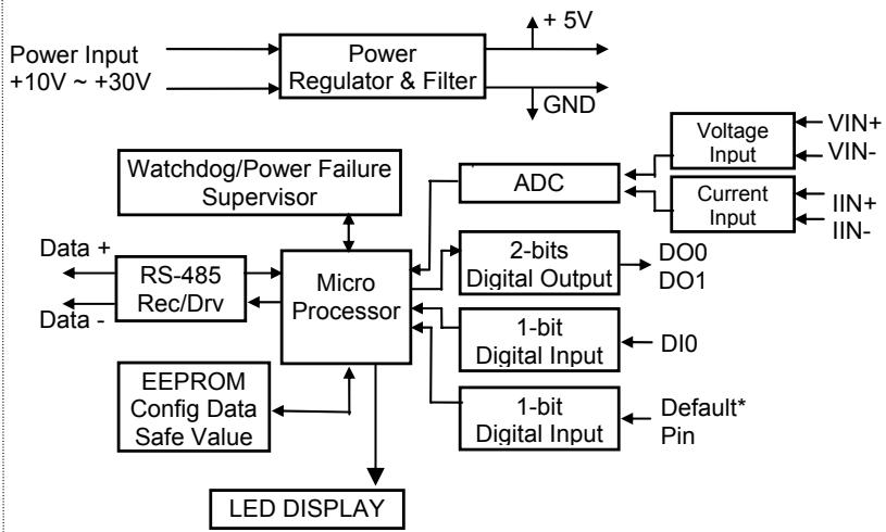
![Based on the provided flowchart, here is the accurate description of the blocks and their connections:\n\n**Power Supply Section:**\n*   **Power Input +10V ~ +30V** connects to the **Power Regulator & Filter**.\n*   The **Power Regulator & Filter** outputs **+ 5V** and **GND**.\n\n**Central Processing and Configuration:**\n*   The **Micro Processor** is the central component with bidirectional connections to the following blocks:\n    *   **Watchdog/Power Failure Supervisor**\n    *   **RS-485 Rec/Drv**: This block has outputs labeled **Data +** and **Data -**.\n    *   **EEPROM Config Data Safe Value**\n    *   **LED DISPLAY** (unidirectional connection pointing downwards)\n\n**Analog and Digital I/O Section:**\n*   The **Micro Processor** connects to the **ADC** block.\n*   The **ADC** connects bidirectionally to:\n    *   **Voltage Input** (which receives inputs **VIN+** and **VIN-**).\n    *   **Current Input** (which receives inputs **IIN+** and **IIN-**).\n*   The **Micro Processor** connects to the **2-bits Digital Output** block, which outputs **DO0** and **DO1**.\n*   The **Micro Processor** connects to two separate **1-bit Digital Input** blocks:\n    *   One block receives **DI0**.\n    *   The other block receives **Default* Pin**.](.nd-6013-manual-2/04f66b5042d38fdc05c45fac7a49861509f0338bf02bf4bc082cb86999aa2d69.jpg)

A Look at ND-6014D & Pin Assignment
![20\nDO1/HI\nDIO/EV\nDOO/LO\n+15V out\nVIN+\nVIN-\nTransmitter\nInput Module\nND-6014D\nCode	mV/mA\n08/09/0A	+10V/25V/+1V\n0B/0C/0D	±500mV/\n	±150mV/\n	+20mV\n+15V out\nIIN+\nIIN-\nDEFAULT*\n(Y)DATA+\n(G)DATA-\n(R)+Vs\n(B)GND\n10](.nd-6013-manual-2/4f7a61dc95d9e9fb3e2aba5e14fe8ebcccf4e5baf8059e465997629e5e5a0e7e.jpg)

# 1.6 Overview of NuDAM-6017

# What is NuDAM-6017?

NuDAM-6017 is an analog input module with 8 input channels. Six of the eight channels are differential type and the other two are single ended type.

# Features of NuDAM-6017

• 8 analog input channels
• 6 differential inputs and 2 single ended inputs
• Programmable input voltage range
• Programmable host watchdog timer for host failure protection
• 5000 Vrms isolation voltage
• Internal watchdog timer for device failure protection
• Easy programming by software
• Easy installation and wiring

# Specifications of NuDAM-6017

# Interface

• Interface: RS-485, 2 wires
• Speed (bps): 1200, 2400, 4800, 9600, 19.2K, 38.4K, 115.2K (115.2K only for firmware reversion above A4.00)

# ✨ Analog Input (4)

• Input type: Differential input
• Channels Numbers: 8
• Resolution: 16 bits
• Unit Conversion: mV, V, or mA
- Voltage Range: Programmable 5 levels, ±10V, ±5V, ±1V, ±500mV, ±150mV
• Current Measurement: ±20mA (with external 125Ω resistor)
• Accuracy: ±0.1%

# Power

• Power supply: +10V to +30V
• Current consumption: 1.2 W

Note $^{(4)}$ : The maximum input voltage shall not exceed to $\pm30V$ with reference to AGND otherwise, they may cause an unrecoverable harm to the hardware component.

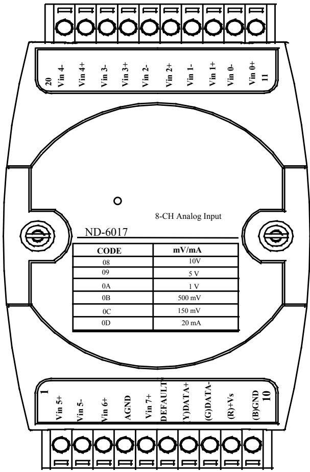
Pin Definitions of ND-6017

<table><tr><td>Pin #</td><td>Signal Name</td><td>Description</td></tr><tr><td>1</td><td>Vin5+</td><td>Differential positive input channel 5</td></tr><tr><td>2</td><td>Vin5-</td><td>Differential negative input channel 5</td></tr><tr><td>3</td><td>Vin6+</td><td>Single-ended voltage input channel 6</td></tr><tr><td>4</td><td>AGND</td><td>Analog signal ground of CH6 &amp; 7</td></tr><tr><td>5</td><td>Vin7+</td><td>Single-ended voltage input channel 7</td></tr><tr><td>6</td><td>DEFAULT*</td><td>Initial state setting</td></tr><tr><td>7</td><td>(Y) DATA+</td><td>RS-485 series signal, positive</td></tr><tr><td>8</td><td>(G) DATA-</td><td>RS-485 series signal, negative</td></tr><tr><td>9</td><td>(R) +Vs</td><td>Power supply, +10V~+30V</td></tr><tr><td>10</td><td>(B) GND</td><td>Ground</td></tr><tr><td>11</td><td>Vin0+</td><td>Differential positive input channel 0</td></tr><tr><td>12</td><td>Vin0-</td><td>Differential negative input channel 0</td></tr><tr><td>13</td><td>Vin1+</td><td>Differential positive input channel 1</td></tr><tr><td>14</td><td>Vin1-</td><td>Differential negative input channel 1</td></tr><tr><td>15</td><td>Vin2+</td><td>Differential positive input channel 2</td></tr><tr><td>16</td><td>Vin2-</td><td>Differential negative input channel 2</td></tr><tr><td>17</td><td>Vin3+</td><td>Differential positive input channel 3</td></tr><tr><td>18</td><td>Vin3-</td><td>Differential negative input channel 3</td></tr><tr><td>19</td><td>Vin4+</td><td>Differential positive input channel 4</td></tr><tr><td>20</td><td>Vin4-</td><td>Differential negative input channel 4</td></tr></table>

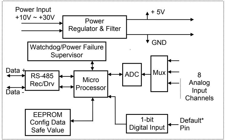
Functional Block Diagram of ND-6017
![Based on the provided flowchart, here are the labeled blocks and their connections:\n\n**Labeled Blocks:**\n*   Power Input +10V ~ +30V\n*   Power Regulator & Filter\n*   Watchdog/Power Failure Supervisor\n*   Data +\n*   RS-485 Rec/Drv\n*   Data -\n*   Micro Processor\n*   ADC\n*   Mux\n*   8 Analog Input Channels\n*   EEPROM Config Data Safe Value\n*   1-bit Digital Input\n*   Default* Pin\n\n**Connections:**\n*   **Power Input +10V ~ +30V** connects to **Power Regulator & Filter**.\n*   **Power Regulator & Filter** outputs **+ 5V** and **GND**.\n*   **Micro Processor** connects bidirectionally to **Watchdog/Power Failure Supervisor**.\n*   **Micro Processor** connects bidirectionally to **RS-485 Rec/Drv**.\n*   **RS-485 Rec/Drv** connects bidirectionally to **Data +** and **Data -**.\n*   **Micro Processor** connects bidirectionally to **ADC**.\n*   **Mux** connects to **ADC** (arrow points from Mux to ADC).\n*   **8 Analog Input Channels** connect to **Mux** (arrows point into Mux).\n*   **Micro Processor** connects to **EEPROM Config Data Safe Value** (arrow points to EEPROM).\n*   **Default* Pin** connects to **1-bit Digital Input**.\n*   **1-bit Digital Input** connects to **Micro Processor** (arrow points to Micro Processor).](.nd-6013-manual-2/061c296e3edce0cf8375b64e5c4a87922ce02c079befa9de2402de416f6c44fc.jpg)

A Look at ND-6017 & Pin Assignment
![20 Vin 4- Vin 4+ Vin 3- Vin 3+ Vin 2- Vin 2+ Vin 1- Vin 1+ Vin 0- Vin 0+ Vin 11\n8-CH Analog Input\nND-6017\nCODE mV/mA\n08 10V\n09 5 V\n0A 1 V\n0B 500 mV\n0C 150 mV\n0D 20 mA\n1 Vin 5+ Vin 5- Vin 6+ AGND Vin 7+ DEFAULT Y)DATA+ (G)DATA- (R)+Vs (B)GND 10](.nd-6013-manual-2/c81557e0cb7c7f2bcb925181d56eb56c0ab3130f0040c391c095c529a16fae18.jpg)

# 1.7 Overview of NuDAM-6018

# What is NuDAM-6018?

NuDAM-6018 is a thermocouple input module with 8 input channels. Six of the eight channels are differential type and the other two are single ended type.

# Features of NuDAM-6018

• 8 analog input channels
• 6 differential inputs and 2 single ended inputs
• Programmable input voltage range
• Programmable host watchdog timer for host failure protection
• On board CJC for temperature measurement
• 2500 Vrms isolation voltage
• Internal watchdog timer for device failure protection
• Easy programming by software
• Easy installation and wiring
• Wiring open detection $^{(5)}$

# Specifications of NuDAM-6018

# Interface

• Interface: RS-485, 2 wires
• Speed (bps): 1200, 2400, 4800, 9600, 19.2K, 38.4K, 115.2K (115.2K only for firmware reversion above A4.00)

# ✨ Analog Input $^{(6)}$

• Input type: Differential input
• Channels Numbers: 8
• Resolution: 16 bits
• Unit Conversion: Thermocouple, mV, V or mA
- Thermocouple Type: J, K, T, E, R, S, B, N, C
J: 0°C\~760°C
K: 0°C\~1370°C $^{(6)}$
T: $-100^{\circ}C \sim 400^{\circ}C$ E: $0^{\circ}C \sim 1000^{\circ}C$
R: 500°C\~1750°C S: 500°C\~1750°C
B: 500°C\~1800°C N: -270°C\~1300°C
C: 0°C\~2320°C

- Voltage Range: Programmable 6 levels ±2.5V, ±1V, ±500mV, ±100mV, ±50mV, ±15mV
• Current Measurement: ±20mA (with external 125Ω resistor)

# Power

• Power supply: +10V to +30V
• Current consumption: 0.9 W

Note $^{(5)}$ : For H/W version B4.0 or above and F/W version B1.31 or above.

Note $^{(6)}$ : The maximum input voltage shall not exceed to $\pm30V$ with reference to AGND otherwise, they may cause an unrecoverable harm to the hardware component.

Note (7): F/W version above C4.30 support K-type for 0\~1370°C. Lower version supports K-type for 0\~1000°C.

Pin Definitions of ND-6018

<table><tr><td>Pin #</td><td>Signal Name</td><td>Description</td></tr><tr><td>1</td><td>Vin5+</td><td>Differential positive input channel 5</td></tr><tr><td>2</td><td>Vin5-</td><td>Differential negative input channel 5</td></tr><tr><td>3</td><td>Vin6+</td><td>Single-ended voltage input channel 6</td></tr><tr><td>4</td><td>AGND</td><td>Analog signal ground of CH6 &amp; 7</td></tr><tr><td>5</td><td>Vin7+</td><td>Single-ended voltage input channel 7</td></tr><tr><td>6</td><td>DEFAULT*</td><td>Initial state setting</td></tr><tr><td>7</td><td>(Y) DATA+</td><td>RS-485 series signal, positive</td></tr><tr><td>8</td><td>(G) DATA-</td><td>RS-485 series signal, negative</td></tr><tr><td>9</td><td>(R) +Vs</td><td>Power supply, +10V~+30V</td></tr><tr><td>10</td><td>(B) GND</td><td>Ground</td></tr><tr><td>11</td><td>Vin0+</td><td>Differential positive input channel 0</td></tr><tr><td>12</td><td>Vin0-</td><td>Differential negative input channel 0</td></tr><tr><td>13</td><td>Vin1+</td><td>Differential positive input channel 1</td></tr><tr><td>14</td><td>Vin1-</td><td>Differential negative input channel 1</td></tr><tr><td>15</td><td>Vin2+</td><td>Differential positive input channel 2</td></tr><tr><td>16</td><td>Vin2-</td><td>Differential negative input channel 2</td></tr><tr><td>17</td><td>Vin3+</td><td>Differential positive input channel 3</td></tr><tr><td>18</td><td>Vin3-</td><td>Differential negative input channel 3</td></tr><tr><td>19</td><td>Vin4+</td><td>Differential positive input channel 4</td></tr><tr><td>20</td><td>Vin4-</td><td>Differential negative input channel 4</td></tr></table>

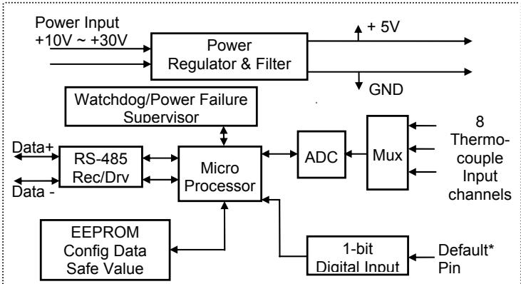
Functional Block Diagram of ND-6018
![**Labeled Blocks and Text:**\n*   Power Input +10V ~ +30V\n*   Power Regulator & Filter\n*   Watchdog/Power Failure Supervisor\n*   RS-485 Rec/Drv\n*   Micro Processor\n*   EEPROM Config Data Safe Value\n*   ADC\n*   Mux\n*   8 Thermocouple Input channels\n*   1-bit Digital Input\n*   Default* Pin\n*   Data+\n*   Data -\n*   + 5V\n*   GND\n\n**Connections:**\n*   **Power Input +10V ~ +30V** connects to the **Power Regulator & Filter**.\n*   The **Power Regulator & Filter** outputs to **+ 5V** and **GND**.\n*   **Watchdog/Power Failure Supervisor** connects bidirectionally to the **Micro Processor**.\n*   **RS-485 Rec/Drv** connects bidirectionally to the **Micro Processor**.\n*   **Data+** and **Data -** connect bidirectionally to the **RS-485 Rec/Drv**.\n*   **EEPROM Config Data Safe Value** connects to the **Micro Processor**.\n*   **1-bit Digital Input** connects to the **Micro Processor**.\n*   **Default* Pin** connects to the **1-bit Digital Input**.\n*   **8 Thermocouple Input channels** connects to the **Mux**.\n*   **Mux** connects to the **ADC**.\n*   **ADC** connects bidirectionally to the **Micro Processor**.](.nd-6013-manual-2/095587b16fe6917f354cffe2a79cd76edb4cd50fb61af991a0a711ecddabbb19.jpg)

A Look at ND-6018 & Pin Assignment
![20 Vin 4- Vin 4+ Vin 3- Vin 3+ Vin 2- Vin 2+ Vin 1- Vin 1+ Vin 0- Vin 0+ 11\nMultiple Analog Input\nND-6018\nCode mV/mA Code T/C\n00 ±15mV 0E J Type\n01 ±50mV 0F K Type\n02 ±100mV 10 T Type\n03 ±500mV 11 E Type\n04 ±1V 12 R Type\n05 ±2.5V 13 S Type\n06 ±20mA 14 B Type\n1 Vin 5+ Vin 5- Vin 6+ AGND Vin 7+ DEFAULT Y)DATA+ (G)DATA- (R)+Vs (B)GND 10](.nd-6013-manual-2/fe50c131cee0529c2dce880fc402f5b7cd939636e0edfd33d7e2f750da249acb.jpg)

# 2

# Initialization & Installation

# 2.1 Software Installation

1. If you have already installed "NuDAM Administration" then skip other steps.
2. Backup your software diskette.
3. Insert "NuDAM Administration" disc into CD-ROM:
4. Change drive to the path of CD-ROM. For example, your drive of CD-ROM is F:, then change the drive to F:
5. Find the setup of NuDAM Administration and run it.
6. Please follow the steps of setup program then you can successful to install the nudism Administration.

# 2.2 Initializing a Brand-New Module

# Objective of Initializing a Brand-New NuDAM

All NuDAM modules, except NuDAM-6520 and NuDAM-6510, in a RS-485 network must have an unique address ID. Every brand-new NuDAM has a factory default setting as following:

- Address ID is 01.
• Baud rate is 9600 bps
- Check-sum disable
• Host Watchdog timer is disable

Therefore, to configure the brand-new NuDAM before using is necessary to avoid conflicting address. The baud rate may also be changed according to user's requirements.

The initialization procedures of a brand-new NuDAM are shown in the following sections. The procedures are applicable for initializing NuDAM-6011/D, NuDAM-6012/D, NuDAM-6013, NuDAM-6014D, NuDAM-6017, and NuDAM-6018.

# Default State

The NuDAM modules must be set at Default State when you want to change the default settings, including the ID address, baud rate, check-sum status etc. All NuDAM modules have an special pin labeled as DEFAULT\*. The module will be in Default State if the Default\*1 pin is shorted to ground when power ON. Under this state, the default configuration is set as following:

- Address ID is 00.
• Baud rate is 9600 bps.
- Check-sum disable.
• Watchdog timer is disable.

Therefore, the configuration of the host and the module can be easily set identically and initializing a module will be possible no matter what configuration is set under operating state.

# Initialization Equipments

• Host computer with an RS-232 port.
• An installed RS-485 module (NuDAM-6520) with 9600 baud rate.
• The brand new NuDAM module
• Power supply (+10 $V_{DC}$ to +30 $V_{DC}$ ) for NuDAM modules
• Administration utility software

Note1: Never Connect the DRFAULT\* pin to Vs or power source just left it open or wired to GND.

# Initialization Procedure

1. Power off the host computer and the installed NuDAM-6520. Be sure of the baud rate of the NuDAM-6520 is 9600 bps.
2. Connect a brand new NuDAM module with the RS-485. Set the module in Default State by shorting the DEFAULT\* pin. Refer to Figure 2.1 for detailed wiring.
3. Power on the host computer.
4. Power on the power supply for NuDAM modules.
5. Use the NuDAM Administration utility to configure the address ID, Baud rate and check-sum status of the module.

# Initialization Wiring
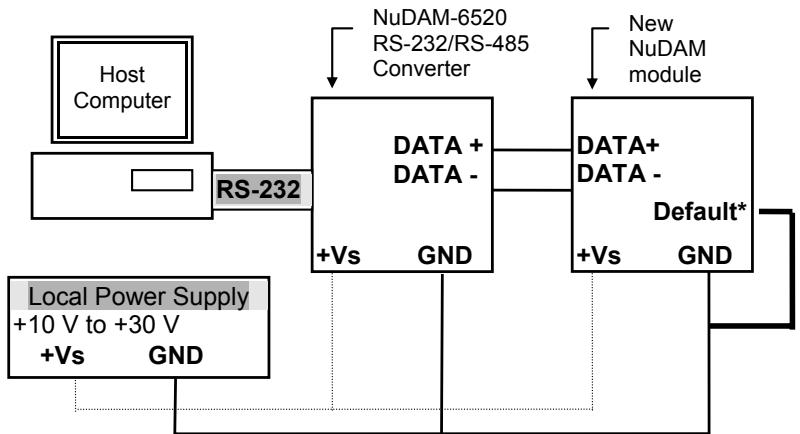
![Based on the provided image, here is an accurate and concise description of the flowchart:\n\n**Labeled Blocks:**\n*   **Host Computer**: A box at the top left containing the text 'Host Computer'.\n*   **Local Power Supply**: A box at the bottom left containing the title 'Local Power Supply', the text '+10 V to +30 V', and the terminals '+Vs' and 'GND'.\n*   **NuDAM-6520 RS-232/RS-485 Converter**: A central box labeled with an arrow pointing down to the text 'NuDAM-6520 RS-232/RS-485 Converter'. Inside the box is the text 'DATA + DATA -' and terminals '+Vs' and 'GND'.\n*   **New NuDAM module**: A box on the right labeled with an arrow pointing down to the text 'New NuDAM module'. Inside the box is the text 'DATA+ DATA -', 'Default*', and terminals '+Vs' and 'GND'.\n\n**Connections:**\n*   **Host Computer to Converter**: A cable labeled 'RS-232' connects the bottom of the Host Computer block to the left side of the NuDAM-6520 converter block.\n*   **Converter to New Module (Data)**: Two horizontal lines connect the right side of the NuDAM-6520 converter to the left side of the New NuDAM module. The top line connects 'DATA +' to 'DATA+' and the bottom line connects 'DATA -' to 'DATA -'.\n*   **Power Connections**:\n    *   A solid line connects the 'GND' of the Local Power Supply to the 'GND' of the NuDAM-6520 converter.\n    *   A dotted line connects the '+Vs' of the Local Power Supply to the '+Vs' of the NuDAM-6520 converter.\n    *   From the NuDAM-6520 converter, a solid line connects its 'GND' terminal to the 'GND' of the New NuDAM module.\n    *   From the NuDAM-6520 converter, a dotted line connects its '+Vs' terminal to the '+Vs' of the New NuDAM module.](.nd-6013-manual-2/154742bc1f1959b6d017e7698f0a0f716325edd8190e0da20a137acbd0f06a12.jpg)

Figure 2-1 Layout for Initialization the NuDAM module

# 2.3 Install a New NuDAM to a Existing Network

# Equipments for Install a New Module

• A existing NuDAM network
• New NuDAM modules
• Power supply (+10 to +30 $V_{DC}$ )

# Installing Procedures

1. Configure the new NuDAM module according to the initialization procedures in section 2.2.
2. The baud rate and check-sum status of the new module must be identity with the existing RS-485 network. The address ID must not be conflict with other NuDAM modules on the network.
3. Power off the NuDAM power supply of the existing RS-485 network.
4. Power off the host computer.
5. Wire the power lines for the new NuDAM with the existing network. Be careful about the signal polarity as wiring.
6. Wire the RS-485 data lines for the new NuDAM with the existing network. Be careful about the signal polarity as wiring.
7. Wire to the input or output devices. Refer to section 2.4 for illustrations.
8. Power on the host computer.
9. Power on the NuDAM local power supply.
10. Use the NuDAM administration utility to check entire network.

# 2.4 Application Wiring for NuDAM-601X

Differential Voltage Input
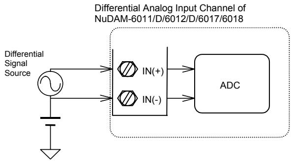
![Based on the provided image, here is the accurate description of the flowchart/block diagram:\n\n**Labels and Blocks:**\n*   **Top Title:** 'Differential Analog Input Channel of NuDAM-6011/D/6012/D/6017/6018'\n*   **Left Label:** 'Differential Signal Source'\n*   **Left Symbols:** An AC voltage source (circle with a sine wave), a DC battery symbol, and a ground symbol.\n*   **Central Block:** A rectangular area containing two input terminals labeled 'IN(+)' (top) and 'IN(-)' (bottom). Each terminal has a hexagonal input symbol.\n*   **Right Block:** A rounded rectangle labeled 'ADC'.\n\n**Connections:**\n*   **Signal Input:** Two lines originate from the AC signal source.\n    *   The top line connects the top of the AC source to the 'IN(+)' terminal with an arrow pointing right.\n    *   The bottom line connects the bottom of the AC source to the 'IN(-)' terminal with an arrow pointing right. (Note: This bottom line also connects to the battery symbol, which leads to ground).\n*   **Internal Processing:** Two arrows originate from the 'IN(+)' and 'IN(-)' terminals and point to the right, entering the 'ADC' block.\n*   **Enclosure:** A dotted line box surrounds the central input terminals and the 'ADC' block, grouping them together under the main title.](.nd-6013-manual-2/e7666ac0b93ff95a6a5f79d590dd83b2f91b6f31509df663683a091b6a1ccb3d.jpg)

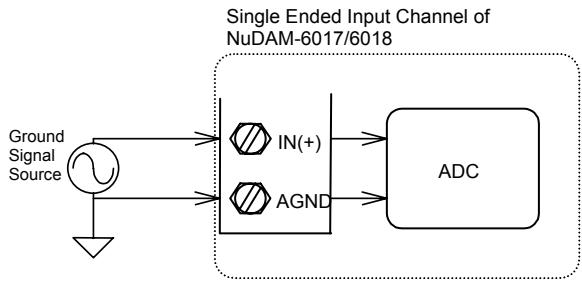
Single Ended Voltage Input
![The diagram depicts a system labeled 'Single Ended Input Channel of NuDAM-6017/6018' enclosed within a dotted boundary. On the left, a 'Ground Signal Source' (represented by an AC voltage source circle) is connected to ground. Two signal lines originate from this source: the top line connects to an input terminal labeled 'IN(+)', and the bottom line connects to a terminal labeled 'AGND'. These terminals are part of a vertical input interface. Two arrows extend from this interface to the right, entering a large rounded block labeled 'ADC'.](.nd-6013-manual-2/64a8b6e6a8426b4b3a20b3f0aee42bd26fa1ae5bdca47c7794dafaabe1c32c10.jpg)

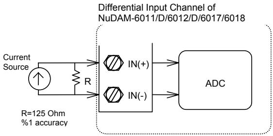
Current Measurement

![The diagram depicts a signal input configuration enclosed within a dotted border labeled 'Differential Input Channel of NuDAM-6011/D/6012/D/6017/6018'.\n\n**Blocks and Labels:**\n*   **Left:** A 'Current Source' (circle with an upward arrow) is connected in parallel with a resistor labeled 'R'. Below this, text reads 'R=125 Ohm' and '%1 accuracy'.\n*   **Center:** A section containing two hexagonal symbols labeled 'IN(+)' and 'IN(-)'.\n*   **Right:** A rounded rectangular block labeled 'ADC'.\n\n**Connections:**\n*   Arrows connect the top and bottom terminals of the 'Current Source' and resistor circuit to the 'IN(+)' and 'IN(-)' inputs, respectively.\n*   Arrows extend from the right side of the 'IN(+)' and 'IN(-)' symbols directly into the left side of the 'ADC' block.](.nd-6013-manual-2/20731cdd403334de6233fc60b916a251c080948f521f8784071283ccfb1f5833.jpg)

Digital Input Connect with TTL Signal
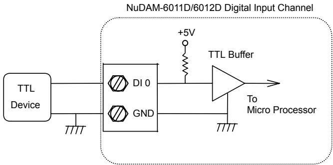
![**Overview**\nThe diagram is titled **NuDAM-6011D/6012D Digital Input Channel** at the top right. A large dotted box encloses the main circuitry.\n\n**Blocks and Connections**\n*   **TTL Device:** A rectangular block on the far left labeled **TTL Device**. It connects via two lines to a central rectangular block.\n*   **Terminals:** The central block inside the dotted box contains two terminals labeled **DI 0** (top) and **GND** (bottom).\n*   **TTL Buffer:**\n    *   The **DI 0** terminal connects to the input of a triangle labeled **TTL Buffer**.\n    *   A resistor connects the label **+5V** to the wire connecting **DI 0** and the buffer.\n    *   A ground symbol connects to the bottom of the **TTL Buffer**.\n    *   The **GND** terminal connects to a separate ground symbol below it.\n*   **Output:** An arrow exits the right side of the **TTL Buffer** pointing to the text **To Micro Processor**.](.nd-6013-manual-2/a513a152251509b83f68e59300ed65df2ae92503d7f51d6ee830cfb922ab2cc9.jpg)

Digital Input Used as an Event Counter
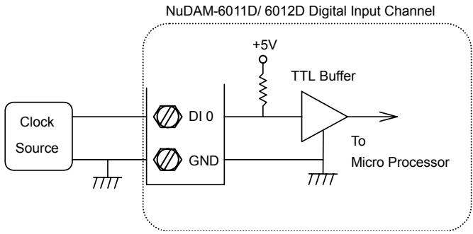
![The diagram is titled '**NuDAM-6011D/ 6012D Digital Input Channel**'. It depicts the following blocks and connections:\n\n*   **Left Block:** A rectangular block labeled '**Clock Source**'.\n    *   A line connects the top of the 'Clock Source' to a terminal labeled '**DI 0**'.\n    *   A line connects the bottom of the 'Clock Source' to a ground symbol and then to a terminal labeled '**GND**'.\n\n*   **Central Circuit (inside dotted box):**\n    *   The '**DI 0**' terminal connects to a wire that is also connected to a resistor coming from '**+5V**'.\n    *   This combined wire connects to the input of a triangle symbol labeled '**TTL Buffer**'.\n    *   The '**GND**' terminal connects to a wire that leads to a ground symbol and connects to the bottom of the '**TTL Buffer**'.\n\n*   **Output:** An arrow points to the right from the '**TTL Buffer**' towards the text '**To Micro Processor**'.](.nd-6013-manual-2/1fa38e81c3d69c7d6c99c3c04ae595389de6e0654daf1cfa7d271a39e87b9e06.jpg)

Digital Output Connect with Power Loading
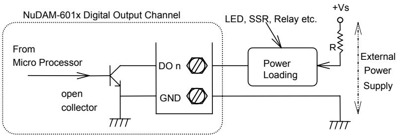
![The image displays a circuit diagram for a digital output channel.\n\n**Labeled Blocks:**\n*   **NuDAM-601x Digital Output Channel:** A large dotted rectangle containing the internal circuitry.\n*   **From Micro Processor:** Text indicating the input signal source.\n*   **open collector:** Text describing the transistor configuration.\n*   **DO n:** A terminal label inside the channel box.\n*   **GND:** A terminal label inside the channel box.\n*   **LED, SSR, Relay etc.:** Text pointing to the load block.\n*   **Power Loading:** A rectangular block representing the external load.\n*   **+Vs:** The voltage supply label.\n*   **R:** A resistor label.\n*   **External Power Supply:** Text describing the power source area.\n\n**Connections:**\n*   An arrow labeled **'From Micro Processor'** points to the base of a transistor.\n*   The transistor's collector connects to the vertical bar labeled **'DO n'**.\n*   The transistor's emitter connects to the vertical bar labeled **'GND'** and to a ground symbol.\n*   A line connects the **'DO n'** terminal to the left side of the **'Power Loading'** block.\n*   A line connects the **'GND'** terminal to a ground symbol on the far right.\n*   The right side of the **'Power Loading'** block connects to a resistor labeled **'R'**.\n*   The resistor **'R'** connects to **'+Vs'**.](.nd-6013-manual-2/3a5c380e87383ed303cc8cd9e8129e268d641aff3a7f52cc34a23289d7aa8f4a.jpg)

R : current limit resistor

RTD Input (NuDAM-6013)
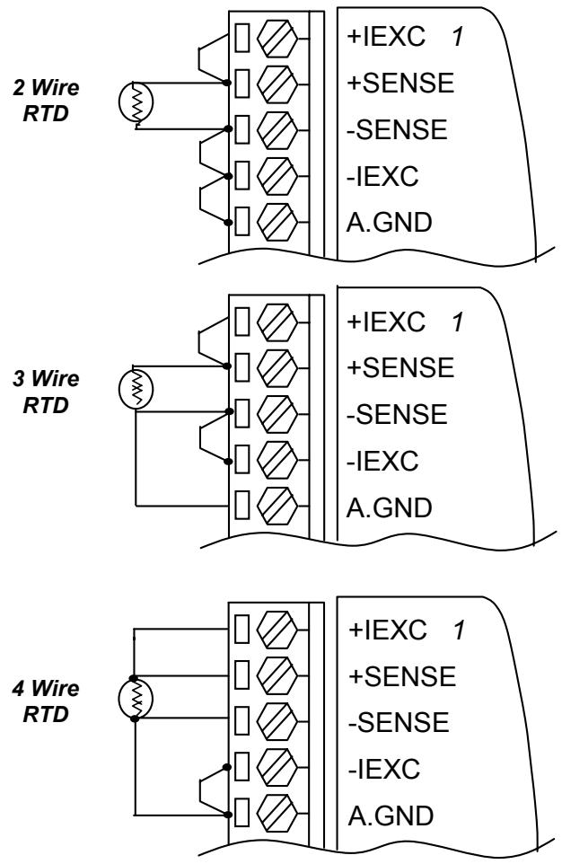
![The image displays three schematic diagrams stacked vertically, illustrating wiring configurations for RTD sensors.\n\n**Top Diagram**\n*   **Left Label:** 2 Wire RTD\n*   **Right Column Text:**\n    +IEXC 1\n    +SENSE\n    -SENSE\n    -IEXC\n    A.GND\n\n**Middle Diagram**\n*   **Left Label:** 3 Wire RTD\n*   **Right Column Text:**\n    +IEXC 1\n    +SENSE\n    -SENSE\n    -IEXC\n    A.GND\n\n**Bottom Diagram**\n*   **Left Label:** 4 Wire RTD\n*   **Right Column Text:**\n    +IEXC 1\n    +SENSE\n    -SENSE\n    -IEXC\n    A.GND\n\nEach diagram features a resistor symbol (a circle containing a zigzag line) connected via lines to a vertical terminal block with rectangular terminals. The text on the right corresponds to these terminals.](.nd-6013-manual-2/fcfdff83b3a76d8108a65eb8ec516866c57bd1664d268920ec8f658cc62eb637.jpg)

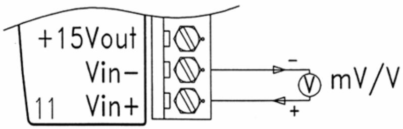
# Application Wiring for NuDAM-6014D

Millivolt and Volt Input
![+15Vout\nVin-\n11 Vin+\nmV/V](.nd-6013-manual-2/f11d321dd4c8ac2f2f41852017671eac9c34994d4d7ad01b4c0756c2e23a89dd.jpg)

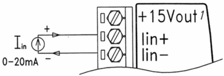
Process Current Input
![Iin\n0-20mA\n+\n-\n+15Vout1\nlin+\nlin-](.nd-6013-manual-2/7278dc584cb0b90ccb39e9d190ba74ee85bb9de8d66463d8d675970a0fc8e02f.jpg)

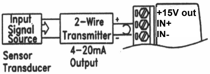
# Transmitter wiring for NuDAM-6014D

2-wire Transmitter Input
![The diagram illustrates a signal transmission process from left to right involving the following labeled blocks and connections:\n\n*   **Left Block:** A rectangle labeled '**Input Signal Source**' with the text '**Sensor Transducer**' directly below it.\n*   **Middle Block:** A rectangle labeled '**2-Wire Transmitter**' with the text '**4-20mA Output**' directly below it.\n*   **Right Block:** A rectangular block on the far right containing the text '**+15V out**' at the top, '**IN+**' in the middle, and '**IN-**' at the bottom.\n*   **Terminal Block:** Between the transmitter and the right block, there is a drawing of a terminal connector with three screw terminals.\n\n**Connections:**\n*   An arrow points from the '**Input Signal Source**' block to the '**2-Wire Transmitter**' block.\n*   Two lines connect the '**2-Wire Transmitter**' to the terminal block. The top line is labeled '**+**' and connects to the top terminal. The bottom line is labeled '**-**' and connects to the bottom terminal.](.nd-6013-manual-2/2a61156ee0a48f9dce86c47355e59a29b09dde3fdfcb142358c15c5d63f02794.jpg)

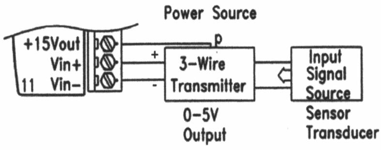
3-wire Transmitter Input
![Based on the provided image, here is the description of the flowchart/block diagram:\n\n**Labeled Blocks and Text:**\n\n*   **Left Block:** A shape resembling a terminal block containing the text '**+15Vout**', '**Vin+**', and '**Vin-**' vertically stacked. To the far left is the number '**11**'. On its right edge are three screw terminals.\n*   **Middle Block:** A rectangular box labeled '**3-Wire Transmitter**'. Below the box is the text '**0-5V Output**'. Above the box is the letter '**p**'.\n*   **Right Block:** A rectangular box labeled '**Input Signal Source**'. Below the box is the text '**Sensor Transducer**'.\n*   **Top Label:** The text '**Power Source**' appears centered at the top of the diagram.\n\n**Connections:**\n\n*   **Left to Middle:** Three horizontal parallel lines connect the three terminals of the left block to the left side of the '**3-Wire Transmitter**'.\n    *   The top line connects to the top of the transmitter box. The letter '**p**' is above this connection point.\n    *   There is a '**+**' sign near the top wire entering the transmitter.\n    *   There is a '**-**' sign near the bottom wire entering the transmitter.\n*   **Middle to Right:** A double-headed arrow connects the right side of the '**3-Wire Transmitter**' to the left side of the '**Input Signal Source**'.](.nd-6013-manual-2/79d718cd0e1c454e6340cbf28290f7b0c0081dbf6e4c6bcb844c9f116290e4aa.jpg)

# 3

# Command Set

# 3.1 Command and Response

# Introduction

The NuDAM command is composed by numbers of characteristics, including the leading code, address ID, the variables, the optional check-sum bytes, and a carriage return to indicate the end of a command. The host computer can only command only one NuDAM module except those synchronized commands with wildcard address “\*\*”. The NuDAM may or may not give response to the command. The host should check the response to handshake with the modules.

# Document Conventions

The following syntax conventions describe the NuDAM commands in this manual.

<table><tr><td>(Leading Code)</td><td>Leading Code is the first characteristic of the NuDAM command. All NuDAM commands need a command leading code, such as %,$,#,@,...etc. 1- character</td></tr><tr><td>(Addr)</td><td>Module&#x27;s address ID, the value is in the range of 00 - FF (Hex). 2- character</td></tr><tr><td>(Command Variable)</td><td>Command codes or value of variables.Variable length</td></tr><tr><td>[Data]</td><td>Some commands need additional data.Variable length</td></tr><tr><td>[Checksum]</td><td>Checksum in brackets indicate optional parameter, only checksum is enable then this field is required. 2- character</td></tr><tr><td>&lt; &gt;</td><td>Identifies a control code character, such asfor carriage return, its value is 0x0D.1- character</td></tr></table>

# Format of NuDAM Commands

(Leading Code)(Addr)(Command)[Data][Checksum]&lt;CR&gt;

When checksum is enable then [Checksum] is needed, it is 2-character. Both command and response must append the checksum characters.

# How to calculate checksum value?

[Checksum] = ((LeadingCode)+(Addr)+(Command)+[Data]) MOD 0x100

Example 1: checksum is disable

<table><tr><td>User Command:</td><td>$012</td></tr><tr><td>Response:</td><td>!01400600</td></tr></table>

<table><tr><td>$</td><td>: LeadingCode</td></tr><tr><td>01</td><td>: Address</td></tr><tr><td>2</td><td>: Command (Read Configuration)</td></tr><tr><td></td><td>: Carriage return 0x0D</td></tr></table>

Example 2: checksum is enable

<table><tr><td>User Command:</td><td>$012B7</td></tr><tr><td>Response:</td><td>!01400600AC</td></tr></table>

<table><tr><td>$</td><td>: LeadingCode</td></tr><tr><td>01</td><td>: Address</td></tr><tr><td>2</td><td>: Command (Read Configuration)</td></tr><tr><td>B7</td><td>: Checksum value</td></tr><tr><td></td><td>: Carriage return 0x0D</td></tr></table>

<table><tr><td>‘$’ = 0x24</td><td>‘0’ = 0x30</td><td>‘1’ = 0x31</td><td>‘2’ = 0x32</td></tr><tr><td colspan="4">B7 = ( 0x24 + 0x30 + 0x31 + 0x32 ) MOD 0x100</td></tr></table>

<table><tr><td>‘!’ = 0x24</td><td>‘0’ = 0x30</td><td>‘1’ = 0x31</td><td>‘4’ = 0x34</td></tr><tr><td>‘6’ = 0x36</td><td></td><td></td><td></td></tr></table>

<table><tr><td> $\mathbf{AC} = (0x24 + 0x30 + 0x31 + 0x34 + 0x30 + 0x30 + 0x36 + 0x30 + 0x30) \text{ MOD } 0x100$ </td></tr></table>

Note: 1. There is no spacing between the command words and The checksum characters.

2. Every command follows a &lt;CR&gt; carriage return for ending.

3. The checksum characters are optional.

# Response of NuDAM Commands

The response message depends on versatile NuDAM command. The response is composed with a few characteristics, including leading code, variables, and carriage return for ending. There are two categories of leading code for response message, "!" or "> means valid command and "?" means invalid. By checking the response message, user can monitor the command is valid or not.

Note: Under the following conditions, there will have no response message.

1. The specified address ID is not exist.

2. Syntax error.

3. Communication error.

4. Some special commands do not have response.

# 3.2 Summary of Command Set

There are three categories of NuDAM commands. The first is the general commands, including set configuration command, read configuration, reset, read module's name or firmware version, etc. Every NuDAM can response to the general commands. The second is the functional commands, which depends on functions of each module. Not every module can execute all function commands. The third is the special commands including functions about the programmable watchdog timer, safe values, and the programmable leading code. All the commands used in the NuDAM analog input module are list in the following table.

<table><tr><td colspan="4">Command Set of Analog Input Modules</td></tr><tr><td>Command</td><td>Syntax</td><td>Modules</td><td>Page</td></tr><tr><td colspan="4">General Commands</td></tr><tr><td>Set Configuration</td><td>%(OldAddr)(NewAddr)(InputRange)(BaudRate)(DataFormat)</td><td>ALL</td><td>3-7</td></tr><tr><td>Read Configuration</td><td>$(Addr)2</td><td>ALL</td><td>3-11</td></tr><tr><td>Read Module Name</td><td>$(Addr)M</td><td>ALL</td><td>3-12</td></tr><tr><td>Read Firmware Version</td><td>$(Addr)F</td><td>ALL</td><td>3-13</td></tr><tr><td>Software Reset</td><td>$(Addr)RS</td><td>ALL(1)</td><td>3-14</td></tr><tr><td colspan="4">Functional Commands</td></tr><tr><td>Synchronized Sampling</td><td>#**</td><td>6011/D, 6012/D, 6014D</td><td>3-15</td></tr><tr><td>Read Synchronized Analog Data</td><td>$(Addr)4</td><td>6011/D, 6012/D, 6014D</td><td>3-16</td></tr><tr><td>Read Analog Data</td><td>#(Addr)</td><td>6011/D, 6012/D, 6014D</td><td>3-17</td></tr><tr><td>Read Analog Data Channel 0</td><td>#(Addr)</td><td>6013</td><td>3-17</td></tr><tr><td>Span Calibration</td><td>$(Addr)0</td><td>ALL</td><td>3-18</td></tr><tr><td>Span Calibration to each Channel</td><td>$(Addr)0(Channel No)</td><td>6013(2)</td><td>3-19</td></tr><tr><td>Offset Calibration</td><td>$(Addr)1</td><td>ALL</td><td>3-20</td></tr><tr><td>Offset Calibration to each Channel</td><td>#(Addr)1(Channel No)</td><td>6013(2)</td><td>3-21</td></tr><tr><td>Read Analog Data From Channel N</td><td>#(Addr)(ChannelNo)</td><td>6013, 6017, 6018</td><td>3-22</td></tr><tr><td>Read All Analog Data</td><td>$(Addr)A</td><td>6013, 6017, 6018</td><td>3-23</td></tr><tr><td>Enable/Disable Channel for Multiplexing</td><td>$(Addr)5(ChannelVal)</td><td>6013, 6017, 6018</td><td>3-24</td></tr><tr><td>Read Channel Status</td><td>$(Addr)6</td><td>6013, 6017, 6018</td><td>3-25</td></tr><tr><td>Read CJC Status</td><td>$(Addr)3</td><td>6011/D, 6018</td><td>3-26</td></tr><tr><td>Enable/Disable CJC</td><td>$(Addr)C(Status)</td><td>6011/D, 6018(3)</td><td>3-27</td></tr><tr><td>Read Enable/Disable CJC Status</td><td>$(Addr)D</td><td>6011/D, 6018(3)</td><td>3-28</td></tr><tr><td>Read Source High/Low Values for Linear Mapping</td><td>$(Addr)3</td><td>6014D</td><td>3-32</td></tr><tr><td>Read Target High/Low Values for Linear Mapping</td><td>$(Addr)5</td><td>6014D</td><td>3-33</td></tr><tr><td>Write Source High/Low Values for Linear Mapping</td><td>$(Addr)6(Data_L)(Data_H)</td><td>6014D</td><td>3-34</td></tr><tr><td>Write Target High/Low Values for Linear Mapping</td><td>$(Addr)7(Data_L)(Data_H)</td><td>6014D</td><td>3-35</td></tr><tr><td>Enable/Disable Linear Mapping</td><td>$(Addr)A(Status)</td><td>6014D</td><td>3-36</td></tr><tr><td>Read Enable/Disable Linear Mapping Status</td><td>$(Addr)R</td><td>6014D</td><td>3-37</td></tr><tr><td>CJC Offset Calibration</td><td>$(Addr)9(Counts)</td><td>6011/D, 6018</td><td>3-38</td></tr><tr><td>Clear Latch Alarm</td><td>@(Addr)CA</td><td>6011/D, 6012/D, 6014D</td><td>3-39</td></tr><tr><td>Clear Event Counter</td><td>@(Addr)CE</td><td>6011/D, 6012/D, 6014D</td><td>3-40</td></tr><tr><td>Disable Alarm</td><td>@(Addr)DA</td><td>6011/D, 6012/D, 6014D</td><td>3-41</td></tr><tr><td>Read Digital I/O and Alarm Status</td><td>@(Addr)DI</td><td>6011/D, 6012/D, 6014D</td><td>3-42</td></tr><tr><td>Set Digital Output</td><td>@(Addr)DO(OutData)</td><td>6011/D, 6012/D, 6014D</td><td>3-44</td></tr><tr><td>Enable Alarm</td><td>@(Addr)EA(Mode)</td><td>6011/D, 6012/D, 6014D</td><td>3-45</td></tr><tr><td>Set High Alarm</td><td>@(Addr)HI(Data)</td><td>6011/D, 6012/D, 6014D</td><td>3-46</td></tr><tr><td>Set Low Alarm</td><td>@(Addr)LO(Data)</td><td>6011/D, 6012/D, 6014D</td><td>3-47</td></tr><tr><td>Read Event Counter</td><td>@(Addr)RE</td><td>6011/D, 6012/D, 6014D</td><td>3-48</td></tr><tr><td>Read High Alarm</td><td>@(Addr)RH</td><td>6011/D, 6012/D, 6014D</td><td>3-49</td></tr><tr><td>Read Low Alarm</td><td>@(Addr)RL</td><td>6011/D, 6012/D, 6014D</td><td>3-50</td></tr><tr><td colspan="4">Special Commands</td></tr><tr><td>Read Command Leading Code Setting</td><td>~(Addr)0</td><td>ALL</td><td>3-51</td></tr><tr><td>Change Command Leading Code Setting</td><td>~(Addr)10(C1)(C2)(C3)(C4)(C5)(C6)</td><td>ALL</td><td>3-53</td></tr><tr><td>Set Host Watchdog / Safety Value</td><td>~(Addr)2(Flag)(TimeOut)(SafeValue)</td><td>ALL</td><td>3-55</td></tr><tr><td>Read Host WatchDog / Safe Value</td><td>~(Addr)3</td><td>ALL</td><td>3-57</td></tr><tr><td>Host is OK</td><td>~**</td><td>ALL</td><td>3-58</td></tr></table>

Note: "ALL" means for ND-6011/D, ND-6012/D, ND-6013, ND-6014D, ND-6017 and ND-6018.

(1) This function only support on F/W version above A4.30.
(2) These two functions only support between F/W versionA3.05 to A4.52.
(3) These two functions support on F/W version above B4.60 of ND-6018 and F/W version above A4.60 of ND-6011.
(4) These two functions support on F/W version above B1.31 of ND-6018 and F/W version above C4.60 of ND-6013.

# 3.3 Set Configuration

(6011/D, 6012/D, 6013

6014D, 6017, 6018)

# @Description

Configure the basic setting of NuDAM, including the address ID, input range, baud rate, and data format. The new configuration will be available after executing the command.

# @Syntax

```asp
%(OldAddr)(NewAddr)(InputRange)(BaudRate)(DataFormat)&lt;CR&gt;
```

<table><tr><td>%(OldAddr)</td><td>Command leading code. (1-character)NuDAM module original address ID. The default address ID of a brand new module is 01. The value range of address ID is 00 to FF in hexadecimal.(2-character)</td></tr><tr><td>(NewAddr)</td><td>New address ID, if you don’t want to change address ID, let new address ID equals to the old one. (2-character)</td></tr><tr><td>(InputRange)</td><td>Define analog input range, refers to Table 3-1 for details. (2-character)</td></tr><tr><td>(BaudRate)</td><td>Define communication baud rate, refers to Table 3-2 for details. (2-character)</td></tr><tr><td>(DataFormat)</td><td>Define checksum, integration time and output data format, refers to Figure 3-1 for details.(2-character)</td></tr></table>

# @Response

```html
!(Addr)&lt;CR&gt;
or
?(Addr)&lt;CR&gt;
>
```

# (Addr)

# Address ID.

! Command is valid.
? Command is invalid, parameter values are invalid, or change the setting without grounding the DEFAULT\* pin.

# Note:

1. When you want to change the checksum or baud rate, the DEFAULT\* pin must be grounded at first.

2. Waiting a maximum of 7 seconds to perform auto calibration and ranging after the analog input module is reconfigured. Please don't execute any other command during this time period.

@Example

<table><tr><td>User command:</td><td>%0130050600</td></tr><tr><td>Response:</td><td>!30</td></tr></table>

<table><tr><td>Item</td><td>Meaning</td><td>Description</td></tr><tr><td>%</td><td>(Leading Code)</td><td>Command leading code.</td></tr><tr><td>01</td><td>(OldAddr)</td><td>Original address ID is 01(Hex).</td></tr><tr><td>30</td><td>(NewAddr)</td><td>New address ID is 30(Hex).</td></tr><tr><td>05</td><td>(InputRange)</td><td>Analog input range is ±2.5V</td></tr><tr><td>06</td><td>(BaudRate)</td><td>Baud rate is 9600.</td></tr><tr><td>00</td><td>(DataFormat)</td><td>00 means data format is engineering units, checksum is disable and integration time is 50 ms (60Hz).</td></tr><tr><td></td><td>Carriage return</td><td>0x0D.</td></tr></table>

<table><tr><td>Code (Hex)</td><td>Input Range</td><td>Modules</td></tr><tr><td>00</td><td>±15 mV</td><td>6011/D,6018</td></tr><tr><td>01</td><td>±50 mV</td><td>6011/D,6018</td></tr><tr><td>02</td><td>±100 mV</td><td>6011/D,6018</td></tr><tr><td>03</td><td>±500 mV</td><td>6011/D,6018</td></tr><tr><td>04</td><td>±1 V</td><td>6011/D,6018</td></tr><tr><td>05</td><td>±2.5 V</td><td>6011/D,6018</td></tr><tr><td>06</td><td>±20 mA(Required 125Ω current conversion resistor.)</td><td>6011/D,6018</td></tr><tr><td>08</td><td>±10 V</td><td>6012/D,6017,6014D</td></tr><tr><td>09</td><td>±5 V</td><td>6012/D,6017,6014D</td></tr><tr><td>0A</td><td>±1 V</td><td>6012/D,6017,6014D</td></tr><tr><td>0B</td><td>±500 mV</td><td>6012/D,6017,6014D</td></tr><tr><td>0C</td><td>±150 mV</td><td>6012/D,6017,6014D</td></tr><tr><td>0D</td><td>±20 mA(Required 125Ω current conversion resistor.)</td><td>6012/D,6017,6014D</td></tr><tr><td>0E</td><td>Type J Thermocouple 0° to 760°C</td><td>6011/D,6018</td></tr><tr><td>0F</td><td>Type K Thermocouple 0° to 1370°C</td><td>6011/D,6018</td></tr><tr><td>10</td><td>Type T Thermocouple -100° to 400°C</td><td>6011/D,6018</td></tr><tr><td>11</td><td>Type E Thermocouple 0° to 1000°C</td><td>6011/D,6018</td></tr><tr><td>12</td><td>Type R Thermocouple 500° to 1750°C</td><td>6011/D,6018</td></tr><tr><td>13</td><td>Type S Thermocouple 500° to 1750°C</td><td>6011/D,6018</td></tr><tr><td>14</td><td>Type B Thermocouple 500° to 1800°C</td><td>6011/D,6018</td></tr><tr><td>15</td><td>Type N Thermocouple -270° to 1300°C</td><td>6011/D,6018</td></tr><tr><td>16</td><td>Type C Thermocouple 0° to 2320°C</td><td>6011/D,6018</td></tr><tr><td>20</td><td>Pt-100, -100°C to +100°C, α=0.00385</td><td>6013</td></tr><tr><td>21</td><td>Pt-100, 0°C to +100°C, α=0.00385</td><td>6013</td></tr><tr><td>22</td><td>Pt-100, 0°C to +200°C, α=0.00385</td><td>6013</td></tr><tr><td>23</td><td>Pt-100, 0°C to +600°C, α=0.00385</td><td>6013</td></tr><tr><td>24</td><td>Pt-100, -100°C to +100°C, α=0.003916</td><td>6013</td></tr><tr><td>25</td><td>Pt-100, 0°C to +100°C, α=0.003916</td><td>6013</td></tr><tr><td>26</td><td>Pt-100, 0°C to +200°C, α=0.003916</td><td>6013</td></tr><tr><td>27</td><td>Pt-100, 0°C to +600°C, α=0.003916</td><td>6013</td></tr><tr><td>28</td><td>Ni-100, 0°C to +100°C</td><td>6013</td></tr><tr><td>29</td><td>Ni-120, 0°C to +100°C</td><td>6013</td></tr><tr><td>2A</td><td>0~60 Ohms</td><td>6013</td></tr></table>

Table 3-1 AD Input Range Setting

<table><tr><td>Code</td><td>Baudrate</td></tr><tr><td>03</td><td>1200 bps</td></tr><tr><td>04</td><td>2400 bps</td></tr><tr><td>05</td><td>4800 bps</td></tr><tr><td>06</td><td>9600 bps</td></tr><tr><td>07</td><td>19200 bps</td></tr><tr><td>08</td><td>38400 bps</td></tr><tr><td>09</td><td>115200 bps</td></tr></table>

Table 3-2 Baud rate setting code

![The diagram illustrates an 8-bit register structure with fields labeled 7 through 0.\n\n*   **Bit 6** connects via a downward arrow to a block labeled **Checksum**. This block contains the text: '0: disable' and '1: enable'.\n*   **Bit 3** connects via an upward arrow to a block labeled **Reserved**. This block contains the text: 'Must to be 0'.\n*   **Bits 1 and 0** connect via an upward arrow to a block labeled **Analog Input Data Format**. This block contains the following text:\n    *   '00: Engineering units'\n    *   '01: % of Full Scale Range'\n    *   '10: Two's complement of hexadecimal'\n    *   '11: Ohms (6013 only)'\n    *   'Note:'\n    *   '6017/6018 only support engineering units.'\n    *   '6013 supports engineering units and ohms display.'](.nd-6013-manual-2/a2cfd888f3da4ac7d3b71bdd4ec39376629535335416cd6329b93f4e9a24a795.jpg)

Figure 3-1 Data Format Setting of Analog Input Modules

# 3.4 Read Configuration

(6011/D, 6012/D, 6013

6014D, 6017, 6018)

# @Description

Read the configuration of module on a specified address ID.

# @Syntax

```txt
$(Addr)2&lt;CR&gt;
$ Command leading code
(Addr) Address ID.
2 Command code for reading configuration
```

# @Response

```txt
!(Addr)(InputRange)(BaudRate)(DataFormat)&lt;CR&gt;
or
?(Addr)&lt;CR
&gt;
```

```txt
! Command is invalid.
? Command is invalid.
(Addr) Address ID.
(InputRange) Current setting of analog voltage input, refers to Table 3-1 for details.
(BaudRate) Current setting of communication baud rate, refers to Table 3-2 for details.
(DataFormat) Current settings of checksum, integration time and output data format, refers to Figure 3-1 for details.
```

# @Example

```txt
User command: $302&lt;CR&gt;
Response: !30050600&lt;CR&gt;
! Command is valid.
30 Address ID.
05 Analog input range is ±2.5 V.
06 Baud rate is 9600 bps.
00 checksum is disable.
```

# 3.5 Read Module Name

(6011/D, 6012/D, 6013

6014D, 6017, 6018)

@Description

Read module name of NuDAM at specified address.

@Syntax
```txt
$(Addr)M&lt;CR&gt;
$ Command leading code.
(Addr) Address ID
M Read module name
```

@Response
```txt
!(Addr)(ModuleName)
&lt;CR&gt;
or
?(Addr)&lt;CR&gt;
!
? (Addr)
(ModuleName)
Command is invalid.
? (Addr)
Address ID.
NuDAM module's name could be
'6011', '6011/D', '6012', '6012/D', '6013', '6017'
or '6018'.
4 or 5 characters
```

@Example
```txt
User command: $30M&lt;CR&gt;
Response: !306011/D&lt;CR&gt;
! Command is valid.
30 Address
6011/D ND-6011/D (Analog Input Module)
```

# 3.6 Read Firmware Version

(6011/D, 6012/D, 6013

6014D, 6017, 6018)

@Description

Read firmware version of NuDAM at specified address.

@Syntax
```txt
$(Addr)F&lt;CR&gt;
```

```txt
$ Command leading code.
(Addr) Address ID
F Read module firmware version.
```

@Response
```txt
!(Addr)(FirmRev) &lt;CR&gt;
or
?(Addr)&lt;CR&gt;
!
? Command is valid.
? Command is invalid.
(Addr) Address ID.
(FirmRev) NuDAM module's firmware version.
```

@Example
```yaml
User command: $30F&lt;CR&gt;
Response: !30A2.10&lt;CR&gt;
```

```txt
! Command is valid.
30 Address
A2.10 Firmware Version
```

# 3.7 Software Reset

(6011/D, 6012/D, 6013

6014D, 6017, 6018)

@Description

To stop current operation, reset the module to initial power on state.

@Syntax
```txt
$(Addr)RS&lt;CR&gt;
$ Command leading code (1 character)
(Addr) Address ID (2 character)
RS Software Reset (2 character)
```

@Response
```txt
!(Addr)&lt;CR&gt;
or
?(Addr)&lt;CR&gt;
!
? (Addr)
Command is valid.
Command is invalid.
Address ID.
)
```

@Example
```txt
User $060RS&lt;CR&gt;
command:
Response: !06&lt;CR&gt;
```

To stop current operation, reset the module to initial power on state for analog input module ND-6013, address ID is 06H.

# 3.8 Synchronized Sampling

(6011/D, 6012/D, 6014D)

# @Description

Synchronized all modules to sample analog input values and stored the values in the module's register at the same time. The sampled data can be read by "Read Synchronized Data" command.

# @Syntax

```txt
#**&lt;CR
&gt;
```

#
\*\*

Command leading code.
Synchronized sampling command

# @Response

Note: Synchronized sampling command has NO response.

# @Example

User command: #\*\*&lt;CR&gt;

# 3.9 Read Synchronized Data

(6011/D, 6012/D, 6014D)

# @Description

After a synchronized sampling command $\#\*\*$ was issued, you can read the sampled value that was stored in the register of the module at specified address.

@Syntax
```erb
$(Addr)4&lt;CR&gt;
$ Command leading code.
(Addr) Address ID
4 Read synchronized data.
```

@Response
```txt
>(Addr)(Status)(Data)&lt;CR&gt;
or
?(Addr)&lt;CR&gt;
> Command is invalid.
? Command is invalid or no synchronized sampling command was issued.
(Addr) Address ID.
(Status) 0: Data has been sent at least once before.
1: Data has been sent for the first time since a synchronized sampling command was issued. (1-character)
(Data) There are four types of Data format, refers to Chapter 4 for details.
```

@Examples
```txt
User command: $064&lt;CR&gt;
Response: >060+1.6888&lt;CR&gt;
```

Read synchronized data at address 06H, analog input module send its analog input data +1.6888 (units). Status is 0 means it has sent the same data at least once. The current units is set by the data format.

```txt
User command: $064&lt;CR&gt;
Response: >061+1.6888&lt;CR&gt;
```

Read synchronized data at address 06H, analog input module send its analog input data +1.6888 (units). Status is 1 means it is the first time that the data has been sent. The current units is set by the data format

# 3.10 Read Analog Data

(6011/D, 6012/D, 6013, 6014D)

# @Description

Read the analog input value from an analog input module at specified address in a NuDAM network. While for ND-6013, it returns the channel 0 analog data.

# @Syntax

```txt
#(Addr)&lt;CR&gt;
```

\#

Command leading code

(Addr)

Address ID

# @Response

```txt
>(InputData)&lt;CR&gt;
```

>

Delimiter character

(InputData)

The input data represents the analog signal. The unit of the digits depends on the data format used.

There are four types of data format. The format is set by the set configuration command.

Delimiter character

# @Example

User command: #06&lt;CR&gt;

Response: >+1.6888&lt;CR&gt;

Read the analog input module data at address 06 (Hex). The analog input module response data is +1.6888 units. The unit depends on the data format.

# 3.11 Span Calibration

(6011/D, 6012/D, 6013 C4.6
6014D, 6017, 6018)

# @Description

To correct the gain errors of AD converter by using the span calibration.

# @Syntax

```txt
$(Addr)0&lt;CR&gt;
```

```txt
$ Command leading code (1 character)
(Addr) Address ID (2 character)
0 Span calibration (1 character)
```

# @Response

```html
!(Addr)&lt;CR&gt;
or
?(Addr)&lt;CR&gt;
>
```

```txt
! Command is valid.
? Command is invalid.
(Addr) Address ID.
```

# @Example

```yaml
User command: $060&lt;CR&gt;
Response: !06&lt;CR&gt;
```

To perform the span calibration for analog input module, address ID is 06H.

Note: To perform the calibration, a proper input signal should be connected to the analog input module. Different input range have different input voltage, detail refer chapter 5 "Calibration".

# 3.12 Span Calibration to each Channel

(for 6013 F/W version A3.05\~A4.60)

# @Description

To correct the gain errors of AD converter by using the span calibration.

# @Syntax

```txt
$(Addr)0(Channel No)&lt;CR&gt;
```

```txt
$ Command leading code (1 character)
(Addr) Address ID (2 character)
0 Span calibration (1 character)
(Channel No) Channel for Calibration (1 character) 0~2
```

# @Response

```html
!(Addr)&lt;CR&gt;
or
?(Addr)&lt;CR&gt;
>
```

```txt
! Command is valid.
? Command is invalid.
(Addr) Address ID.
```

# @Example

```yaml
User command: $0601&lt;CR&gt;
Response: !06&lt;CR&gt;
```

To perform the span calibration for analog input module ND-6013 channel 1, address ID is 06H.

Note: To perform the calibration, a proper input signal should be connected to the analog input module. Different input range have different input voltage, detail refer chapter 5 "Calibration".

# 3.13 Offset Calibration

(6011/D, 6012/D, 6013 C4.6

and above, 6014D, 6017, 6018)

# @Description

To correct the offset errors of AD converter by using the offset calibration.

# @Syntax

```txt
$(Addr)1&lt;CR&gt;
```

<table><tr><td>$</td><td>Command leading code</td></tr><tr><td>(Addr)</td><td>Address ID</td></tr><tr><td>1</td><td>Offset calibration.</td></tr></table>

# @Response

```html
!(Addr)&lt;CR&gt;
or
?(Addr)&lt;CR&gt;
>
```

<table><tr><td>!</td><td>Command is valid.</td></tr><tr><td>?</td><td>Command is invalid.</td></tr><tr><td>(Addr)</td><td>Address ID.</td></tr></table>

# @Example

<table><tr><td>User command:</td><td>$061</td></tr><tr><td>Response:</td><td>!06</td></tr></table>

To perform the offset calibration for analog input module at specified address 06 (Hex).

<table><tr><td>Note:</td><td>To perform the calibration, a proper input signal should be connected to the analog input module. Different input range have different input voltage, detail refer chapter 5 “Calibration”.</td></tr></table>

# 3.14 Offset Calibration to each Channel (6013)

(for 6013 F/W version A3.05\~A4.60)

# @Description

To correct the offset errors of AD converter by using the offset calibration.

# @Syntax

\$(Addr)1(Channel No)&lt;CR&gt;
```txt
$ Command leading code
(Addr) Address ID
1 Offset calibration.
(Channel No) Channel for calibration.(1 character)0~2
```

# @Response

```html
!(Addr)&lt;CR&gt;
or
?(Addr)&lt;CR&gt;
>
```

```txt
! Command is valid.
? Command is invalid.
(Addr) Address ID.
```

# @Example

```yaml
User command: $0612&lt;CR&gt;
Response: !06&lt;CR&gt;
```

To perform the offset calibration for analog input module ND-6013 channel 2 at specified address 06 (Hex).

Note: To perform the calibration, a proper input signal should be connected to the analog input module. Different input range have different input voltage, detail refer chapter 5 "Calibration".

# 3.15 Read Analog Data From Channel N (6013, 6017, 6018)

# @Description

Read the analog input value of a specified AD channel from an analog input module at specified address in a NuDAM network.

# @Syntax

```txt
#(Addr)(ChannelNo)&lt;CR&gt;
```

<table><tr><td>#</td><td>Command leading code. (1-character)</td></tr><tr><td>(Addr)</td><td>Address ID. (2-character)</td></tr><tr><td>(ChannelNo)</td><td>Channel number, range (0 - 7). (1-character)Range (0-2). For ND-6013</td></tr></table>

# @Response

```txt
>(InputData)&lt;CR&gt;
```

<table><tr><td>&gt;(InputData)</td><td>Delimiter characterInput value from a specified channel number, the data format is a + or - sign with five decimal digits and a fixed decimal point.</td></tr></table>

# @Example

```txt
User command: #061&lt;CR&gt;
Response: >+1.6888&lt;CR&gt;
```

Read the analog input channel 1 of AD module at address 06 (Hexadecimal) in the network. The analog input data is +1.6888 Volts (Data format is engineering unit)

# 3.16 Read All Analog Data Channel

(6013, 6017, 6018)

# @Description

Read all the enable analog input channel value of a specified from an analog input module at specified address in a NuDAM network.

# @Syntax

```txt
#(Addr)A&lt;CR&gt;
```

<table><tr><td>#</td><td>Command leading code. (1-character)</td></tr><tr><td>(Addr)</td><td>Address ID. (2-character)</td></tr><tr><td>A</td><td>All the enable channel</td></tr></table>

# @Response

```asp
>(InputData)(InputData)(InputData)&lt;CR&gt;
```

> Delimiter character

(InputData) Input value from a specified channel number, the data format is a + or - sign with five decimal digits and a fixed decimal point.

# @Example

```txt
User command: #06A&lt;CR&gt;
Response: >+100.88+020.66+006.79&lt;CR&gt;
```

Read the analog input of AD module at address 06 (Hexadecimal) in the network. The analog input data are +100.88 °C for channel 0, +020.66 °C for channel 1 and +006.79°C for channel 3. (Data format is engineering unit).

# 3.17 Enable/Disable channels for Multiplexing

(6013, 6017, 6018)

# @Description

Enable/Disable multiplexing simultaneously for individual channel.

# @Syntax

\$(Addr)5(ChannelVal)&lt;CR&gt;
$ Command leading code. (1-character)
(Addr) Address ID (2-character)
5 Enable/Disable channel. (1-character)
(ChannelVal) bit 3~0 of 1st character: control channel 7 - 4.
bit 3~0 of 2nd character: control channel 3 - 0.
bit value 0: Disable channel
bit value 1: Enable channel (2-character)

# @Response

!(Addr)&lt;CR&gt;
or
?(Addr)&lt;CR&gt;
>

! Command is valid.
? Command is invalid.
(Addr) Address ID.

# @Example

User command: $06548&lt;CR&gt;
Response: !06&lt;CR&gt;

$ Command leading code.
06 Address ID.
5 Disable/Enable channel.
48 Channel Value is 0x48.
‘48’ is 01001000 that means enable channel 3 and channel 6, the other channels are all disable.

# 3.18 Read Channel Status

(6013, 6017, 6018)

# @Description

Read the enable/disable status the channels of ND-6013, ND-6017 or 6018.

# @Syntax

```txt
$(Addr)6&lt;CR&gt;
```

<table><tr><td>$</td><td>Command leading code. (1-character)</td></tr><tr><td>(Addr)</td><td>Address ID (2-character)</td></tr><tr><td>6</td><td>Read channel status. (1-character)</td></tr></table>

# @Response

```txt
!(Addr)(ChannelVal)&lt;CR&gt;
```

or

```txt
?(Addr)&lt;CR
```

&gt;

<table><tr><td>!</td><td>Command is invalid.</td></tr><tr><td>?</td><td>Command is invalid.</td></tr><tr><td>(Addr)</td><td>Address ID.</td></tr><tr><td>(ChannelVal)</td><td>bit 3~0 of 1st character: control channel 7 - 4.bit 3~0 of 2nd character: control channel 3 - 0.bit value 0: Disable channelbit value 1: Enable channel (2-character)</td></tr></table>

# @Example

```txt
User command: $066&lt;CR&gt;
```

```txt
Response: !0648&lt;CR&gt;
```

4 is equals binary 0100 that means enable channel 6 and disable channel 7, 5, 4.
8 is equals binary 1000 that means enable channel 3 and disable channel 2, 1, 0.

# 3.19 Read CJC Status

(6011/D, 6018)

@Description

Read the CJC (Cold Junction Compensation) sensors data.

@Syntax
```txt
$(Addr)3&lt;CR&gt;
```

```txt
$ Command leading code.
(Addr) Address ID
3 Read CJC status.
```

@Response
```html
>(Data)&lt;CR&gt;
or
?(Addr)&lt;CR&gt;
>
```

```txt
> Command is invalid.
(Data) CJC sensor's data.
Data format is engineering units. (an + or - sign with five decimal digits and a decimal fixed point. The resolution is 0.1°C
? Command is invalid.
(Addr) Address ID.
```

@Example
```txt
User command: $063&lt;CR&gt;
Response: >+0037.9&lt;CR&gt;
```

This command is to read analog input module CJC status at address 06H, return data is 37.9°C.

# 3.20 Enable/Disable CJC

(6011/D, 6018)

@Description

To disable/enable CJC of ND-6011/D and ND-6018

@Syntax
```txt
$(Addr)C(Status)&lt;CR&gt;
$ Command leading code (1 character)
(Addr) Address ID (2 character)
C Disable/enable CJC command (1 character)
(Status) 0: Disable
1: Enable
```

@Response
```txt
!(Addr)&lt;CR&gt;
or
?(Addr)&lt;CR&gt;
!
? (Addr)
Command is valid.
? Command is invalid.
Address ID (2 character)
))
```

@Example
```yaml
User $02C1&lt;CR&gt;
command:
Response: !02&lt;CR&gt;
```

To enable CJC and module's address is 02H.

# 3.21 Read enable/disable CJC Status

(6011/D, 6018)

# @Description

To read CJC disable/enable status of ND-6018

# @Syntax

```txt
$(Addr)D&lt;CR&gt;
```

```txt
$ Command leading code (1 character)
(Addr) Address ID (2 character)
D Read CJC disable/enable staus command (1 character)
```

# @Response

```txt
!(Addr)(Status)&lt;CR&gt;
```

or

```txt
?(Addr)&lt;CR&gt;
```

```txt
! Command is valid.
? Command is invalid.
(Stat 0: Disable
us) 1: Enable
```

# @Example

```txt
User $02D&lt;CR&gt;
command:
Response: !021&lt;CR&gt;
```

To read CJC disable/enable status, and module's address is 02H., the CJC is enable.

# 3.22 Read Source High/Low Values for Linear Mapping (6014D)

# @Description

Read the high/low limit values from input for linear mapping.

# @Syntax

```txt
$(Addr)3&lt;CR&gt;
```

\$ Command leading code.

(Addr) Address ID

3 Read the high/low limit values from input for linear mapping.

# @Response

```txt
!(Addr)(Data_L)(Data_H)&lt;CR&gt;
or
?(Addr)&lt;CR&gt;
```

! Command is invalid.

(Addr) Address ID.

(Data\_L) Low limit value for linear mapping.

Data format is with an + or - sign with five decimal digits and a decimal fixed point.

(Data\_H) High limit value for linear mapping.

Data format is with an + or - sign with five decimal digits and a decimal fixed point.

? Command is invalid.

# @Example

```yaml
User command: $023&lt;CR&gt;
Response: !02+04.000+20.000&lt;CR&gt;
```

The module is configured for +20\~-20mA input current range. The linear mapping function should already have been executed. This command is to read the high/low values for linear mapping. The high limit value is +20mA and low limit value is +4mA. The address of this module is 06H.

# 3.23 Read Target High/Low Values for Linear Mapping (6014D)

# @Description

Read the mapped high/low limit values from input for linear mapping.

# @Syntax

```txt
$(Addr)5&lt;CR&gt;
```

\$ Command leading code.

(Addr) Address ID

5 Read the mapped high/low limit values from input for linear mapping.

# @Response

```txt
!(Addr)(Data_L)(Data_H)&lt;CR&gt;
or
?(Addr)&lt;CR&gt;
```

! Command is invalid.

(Addr) Address ID.

(Data\_L) Mapped low limit value for linear mapping.

Data format is with an + or - sign with five decimal digits and a decimal fixed point.

(Data\_H) Mapped high limit value for linear mapping.

Data format is with an + or - sign with five decimal digits and a decimal fixed point.

? Command is invalid.

# @Example

```txt
User command: $055&lt;CR&gt;
Response: !05-20.000+20.000&lt;CR&gt;
```

The module is configured for +20\~-20mA input current range. The linear mapping function had been executed. This command is to read the mapped high/low values for linear mapping. The mapped high limit value is +20mA and mapped low limit value is -20mA. The address of this module is 05H.

# 3.24 Write Source High/Low Values for Linear Mapping (6014D)

# @Description

Write the source high/low limit values from input for linear mapping.

# @Syntax

```txt
$(Addr)6(Data_L)(Data_H)&lt;CR&gt;
```

\$ Command leading code.

(Addr) Address ID

6 Set the high/low limit values from input for linear mapping.

(Data\_L) Low limit input value for linear mapping. It must be lower than the high limit input value. The format of data is the same as input current range. The minimum input value could equal to the minimum input value of input current range. Data format is with an + or - sign with five decimal digits and a decimal fixed point.

(Data\_H) High limit input value for linear mapping. It must be higher than the low limit input value. The format of data is the same as input current range. The maximum input value could equal to the maximum input value of input current range. Data format is with an + or - sign with five decimal digits and a decimal fixed point.

# @Response

```txt
!(Addr)&lt;CR&gt; or ?(Addr)&lt;CR&gt;
```

! Command is invalid.

(Addr) Address ID.

? Command is invalid.

# @Example

User command: \$036-100.00+100.00&lt;CR&gt;

Response: !03&lt;CR&gt;

The module is configured for +150\~-150mV input range. This command is to set the input high/low values from +100.00 to -100.00mV for linear mapping. The address of this module is 05H.

# 3.25 Write Target High/Low Values for Linear Mapping (6014D)

# @Description

Write the target high/low limit values from input for linear mapping.

# @Syntax

```txt
$(Addr)7(Data_L)(Data_H)&lt;CR&gt;
```

\$ Command leading code.

(Addr) Address ID

7 Set the mapped high/low limit values from input for linear mapping.

(Data\_L) Mapped low limit input value for linear mapping. It must be lower than the mapped high limit input value. Data format is with an + or - sign with five decimal digits and a decimal fixed point.

(Data\_H) Mapped high limit input value for linear mapping. It must be Higher than mapped the low limit input value. Data format is with an + or - sign with five decimal digits and a decimal fixed point.

# @Response

```txt
!(Addr)&lt;CR&gt;
or
?(Addr)&lt;CR&gt;
```

! Command is invalid.

(Addr) Address ID.

? Command is invalid.

# @Example

User command: \$036-100.00+100.00&lt;CR&gt;

Response: !03&lt;CR&gt;

The module is configured for +150\~-150mV input range. This command is to set the input high/low values from +100.00 to -100.00mV for linear mapping. The address of this module is 03H.

# 3.26 Enable/Disable Linear Mapping

(6014D)

# @Description

Enable or disable the linear mapping function for the module.

# @Syntax

```txt
$(Addr)A(Status)&lt;CR&gt;
```

\$ Command leading code.

(Addr) Address ID

A Reference to control the linear mapping function.

(Status) One char to determine the linear mapping function enable or disable.

1: means enable.

0: means disable.

# @Response

```txt
!(Addr)&lt;CR&gt;
or
?(Addr)&lt;CR&gt;
```

! Command is invalid.

(Addr) Address ID.

? Command is invalid.

# @Example

User command: \$03A1&lt;CR&gt;

Response: !03&lt;CR&gt;

This command set the linear mapping function of ND-6014D is enable, and the address of this module is 03H.

# 3.27 Read enable/Disable Linear Mapping Status

(6014D)

@Description

Read enable or disable the linear mapping status for the module.

@Syntax

```txt
$(Addr)R&lt;CR&gt;
```

\$ Command leading code.

(Addr) Address ID

R Read to the linear mapping status.

@Response

```txt
!(Addr)(Status)&lt;CR&gt;
or
?(Addr)&lt;CR&gt;
```

! Command is invalid.

(Addr) Address ID.

(Status) One char to means the state of linear mapping.

1: means enable.

0: means disable.

? Command is invalid.

@Example

```txt
User command: $07R&lt;CR&gt;
Response: !070&lt;CR&gt;
```

This command means the linear mapping function of ND-6014D is disable, and the address of this module is 07H.

# 3.28 CJC Offset Calibration

(6011/D, 6018)

# @Description

To correct the CJC offset errors use CJC (Cold Junction Compensation) offset calibration.

# @Syntax

\$(Addr)9(Counts)&lt;CR&gt;
```txt
$ Command leading code
(Addr) Address ID
9 CJC offset calibration.
(Counts) It is a 4-characters (Hexadecimal) with a sign + or -, range is 0000 to FFFF, each count equals approximately 0.0153°C.
Example: +0042 = 4x16 + 2 = 66
66 * 0.0153°C = 1.009°C
```

# @Response

```html
!(Addr)&lt;CR&gt;
or
?(Addr)&lt;CR&gt;
>
```

```txt
! Command is valid.
? Command is invalid.
(Addr) Address ID.
```

# @Example

```txt
User command: $089+0042&lt;CR&gt;
Response: !08&lt;CR&gt;
```

CJC offset calibration at address 08H. The calibrated offset temperature is +0042(Hex) = 66, 66 x 0.0153°C = 1.009°C

# 3.29 Clear Latched Alarm

(6011/D, 6012/D, 6014D)

@Description

Clear the High/Low alarm state at specified analog input module.

@Syntax

@(Addr)CA&lt;CR&gt;

<table><tr><td>@</td><td>Command leading code.</td></tr><tr><td>(Addr)</td><td>Address ID</td></tr><tr><td>CA</td><td>Clear latched alarm.</td></tr></table>

@Response

!(Addr)&lt;CR&gt;

<table><tr><td>!</td><td>Command is valid.</td></tr><tr><td>(Addr)</td><td>Address ID.</td></tr></table>

@Example

<table><tr><td>User command:</td><td>@06CA</td></tr><tr><td>Response:</td><td>!06</td></tr></table>

Clear the both High/Low latch alarm state at address 06H.

# 3.30 Clear Event Counter

(6011/D, 6012/D, 6014D)

# @Description

Reset the event counter to zero at specified analog input module.

# @Syntax

@(Addr)CE&lt;CR&gt;

<table><tr><td>@</td><td>Command leading code.</td></tr><tr><td>(Addr)</td><td>Address ID</td></tr><tr><td>CE</td><td>Clear event counter.</td></tr></table>

# @Response

!(Addr)&lt;CR&gt;

<table><tr><td>!</td><td>Command is valid.</td></tr><tr><td>(Addr)</td><td>Address ID.</td></tr></table>

# @Example

<table><tr><td>User command:</td><td>@06CE&lt;CR&gt;</td></tr><tr><td>Response:</td><td>!06&lt;CR&gt;</td></tr></table>

Set the event counter to zero at address 06H, response data means its event counter has been reset.

# 3.31 Disable Alarm

(6011/D, 6012/D, 6014D)

@Description

Disable High/Low alarm functions at specified analog input module.

@Syntax

@(Addr)DA&lt;CR&gt;

<table><tr><td>@</td><td>Command leading code.</td></tr><tr><td>(Addr)</td><td>Address ID</td></tr><tr><td>DA</td><td>Disable Alarm.</td></tr></table>

@Response

!(Addr)&lt;CR&gt;

<table><tr><td>!</td><td>Command is valid.</td></tr><tr><td>(Addr)</td><td>Address ID.</td></tr></table>

@Example

<table><tr><td>User command:</td><td>@06DA&lt;CR&gt;</td></tr><tr><td>Response:</td><td>!06&lt;CR&gt;</td></tr></table>

Disable all alarm functions at address 06H.

# 3.32 Read Digital I/O and Alarm Status (6011/D, 6012/D, 6014D)

# @Description

Read the digital input channel, digital output channel and the alarm state at specified analog input module.

# @Syntax

@(Addr)DI&lt;CR&gt;

@ Command leading code.

(Addr) Address ID

DI Read digital I/O and alarm state.

# @Response

!(Addr)(Alarm)(DigitalO)(Digitall)&lt;CR&gt;

! Command is invalid.

(Addr) Address ID.

(Alarm) 0: alarm is disable

1: MOMENTARY mode enable.

2: LATCH mode enable.

(1-character)

(DigitalO) Digital output channel, port 0 and 1 status.

00: channel 0 is OFF, channel 1 is OFF

01: channel 0 is ON , channel 1 is OFF

02: channel 0 is OFF, channel 1 is ON

03: channel 0 is ON , channel 1 is ON

(2-character)

(Digitall) Digital input channel, port status.

00: channel is LOW.

01: channel is HIGH.

(2-character)

<table><tr><td>User command:</td><td>@06DI</td></tr><tr><td>Response:</td><td>!0620301</td></tr></table>

<table><tr><td>Item</td><td>Meaning</td><td>Description</td></tr><tr><td>!</td><td>(Leading Code)</td><td>Command leading code.</td></tr><tr><td>06</td><td>(Addr)</td><td>Analog module&#x27;s address ID is 06H.</td></tr><tr><td>2</td><td>(Alarm)</td><td>2 means alarm state is LATCH.</td></tr><tr><td>03</td><td>(DigitalO)</td><td>Digital output channel status.03: channel 0 is ONchannel 1 is ON</td></tr><tr><td>01</td><td>(Digitall)</td><td>Digital input channel status01: digital input is HIGH.</td></tr></table>

Read digital I/O and alarm at address 06H. alarm state is LATCH, digital output channel port 0 and 1 are ON and digital input channel is HIGH.

# 3.33 Set Digital Output

(6011/D, 6012/D, 6014D)

# @Description

Set digital output channel at specified module.

# @Syntax

@(Addr)DO(OutData)&lt;CR&gt;
```txt
@ Command leading code.
(Addr) Address ID
DO Set digital output
(OutData) Digital output data .(2 - characters)
00: bit 1 is OFF, bit 0 is OFF.
01: bit 1 is OFF, bit 0 is ON.
02: bit 1 is ON, bit 0 is OFF
03: bit 1 is ON, bit 0 is ON.
```

@Response
```html
!(Addr)&lt;CR&gt;
or
?(Addr)&lt;CR&gt;
>
```

```txt
! Command is valid.
? Command is invalid.
(Addr) Address ID.
```

@Example
```txt
User command: @06DO02&lt;CR&gt;
Response: !06&lt;CR&gt;
```

Set the digital output channel state at address 06H, digital output channel port 0 is OFF, port 1 is ON.

# 3.34 Enable Alarm

(6011/D, 6012/D, 6014D)

# @Description

Enable alarm to Latch mode or Momentary mode at specified analog input module.

# @Syntax

@(Addr)EA(Mode)&lt;CR&gt;

@ Command leading code.

(Addr) Address ID

EA Enable alarm command code

(Mode) M: enable alarm to MOMENTARY mode.

L: enable alarm to LATCH mode.

# @Response

!(Addr)&lt;CR&gt;

! Command is valid.

(Addr) Address ID.

# @Example

User command: @06EAL&lt;CR&gt;

Response: !06&lt;CR&gt;

Enable alarm to LATCH mode at address 06H.

User command: @06EAM&lt;CR&gt;

Response: !06&lt;CR&gt;

Enable alarm to MOMENTARY mode at address 06H.

# 3.35 Set High Alarm

(6011/D, 6012/D, 6014D)

# @Description

Set high alarm limit value at specified analog input module.

# @Syntax

@(Addr)HI(Data)&lt;CR&gt;

@ Command leading code.

(Addr) Address ID

HI Set high alarm limit value.

(Data) Alarm high limit value.

Data format is engineering units. (an + or - sign with five decimal digits and a decimal fixed point.

# @Response

!(Addr)&lt;CR&gt;

! Command is valid.

(Addr) Address ID.

# @Example

User command: @06HI+300.00&lt;CR&gt;

Response: !06&lt;CR&gt;

Set high alarm limit value to $300^{\circ}$ C for type J thermocouple to input at address 06H.

# 3.36 Set Low Alarm

(6011/D, 6012/D, 6014D)

# @Description

Set low alarm limit value at specified analog input module.

# @Syntax

@(Addr)LO(Data)&lt;CR&gt;

@ Command leading code

(Addr) Address ID

LO Set low alarm limit value.

(Data) Alarm low limit value.

Data format is engineering units. (an + or - sign with five decimal digits and a decimal fixed point.

# @Response

!(Addr)&lt;CR&gt;

! Command is valid.

(Addr) Address ID.

# @Example

User command: @06LO+100.00&lt;CR&gt;

Response: !06&lt;CR&gt;

Set low alarm limit value to +100°C to accept J-type thermocouple input at address 06H.

# 3.37 Read Event Counter

(6011/D, 6012/D, 6014D)

# @Description

Read the event counter value at specified analog input module.

# @Syntax

@(Addr)RE&lt;CR&gt;

<table><tr><td>@</td><td>Command leading code.</td></tr><tr><td>(Addr)</td><td>Address ID</td></tr><tr><td>RE</td><td>Read event counter.</td></tr></table>

# @Response

!(Addr)(Data)&lt;CR&gt;

<table><tr><td>!</td><td>Command is valid.</td></tr><tr><td>(Addr)</td><td>Address ID.</td></tr><tr><td>(Data)</td><td>5-character (Decimal), range 00000 to 65535, if the event counter exceed 65535 then event counter value is 65535 (No changed).</td></tr><tr><td></td><td>(5-character)</td></tr></table>

# @Example

<table><tr><td>User command:</td><td>@06RE</td></tr><tr><td>Response:</td><td>!0612345</td></tr></table>

Read event counter, its value is 12345 (Decimal) at address 06H.

# 3.38 Read High Alarm Limit

(6011/D, 6012/D, 6014D)

# @Description

Read the high alarm limit at specified analog input module.

# @Syntax

@(Addr)RH&lt;CR&gt;

<table><tr><td>@</td><td>Command leading code.</td></tr><tr><td>(Addr)</td><td>Address ID</td></tr><tr><td>RH</td><td>Read high alarm limit.</td></tr></table>

# @Response

!(Addr)(Data)&lt;CR&gt;

<table><tr><td>!</td><td>Command is valid.</td></tr><tr><td>(Addr)</td><td>Address ID.</td></tr><tr><td>(Data)</td><td>High alarm limit value.</td></tr><tr><td></td><td>Data format is engineering units. (an + or - sign with five decimal digits and a decimal fixed point.</td></tr></table>

# @Example

<table><tr><td>User command:</td><td>@06RH</td></tr><tr><td>Response:</td><td>!06+01.500</td></tr></table>

Read the high alarm limit value at address 06H, its value is 1.500 Volts, presume this module is configured to accept $\pm2.5$ Volts input.

# 3.39 Read Low Alarm Limit

(6011/D, 6012/D, 6014D)

# @Description

Read the low alarm limit at specified analog input module.

# @Syntax

@(Addr)RL&lt;CR&gt;

<table><tr><td>@</td><td>Command leading code.</td></tr><tr><td>(Addr)</td><td>Address ID, range (00 - FF).</td></tr><tr><td>RL</td><td>Read low alarm limit.</td></tr></table>

# @Response

!(Addr)(Data)&lt;CR&gt;

<table><tr><td>!</td><td>Command is valid.</td></tr><tr><td>(Addr)</td><td>Address ID.</td></tr><tr><td>(Data)</td><td>Alarm low limit value.</td></tr><tr><td></td><td>Data format is engineering units. (an + or - sign with five decimal digits and a decimal fixed point.</td></tr></table>

# @Example

<table><tr><td>User command:</td><td>@06RL</td></tr><tr><td>Response:</td><td>!06-0.3850</td></tr></table>

Read the low alarm limit value at address 06H, its value is -0.3850 Volts, presume this module is configured to accept 1 Volts input.

# 3.40 Read Leading Code Setting

(6011/D, 6012/D, 6013

6014D, 6017, 6018)

# @Description

Read command leading code setting and host watchdog status.

@Syntax
```txt
~(Addr)0&lt;CR
~
(Addr)
0
Command leading code.
Address ID
Read command leading code setting.
```

@Response
```lisp
!(Addr)(Status)(C1)(C2)(C3)(C4)(C5)(C6)&lt;CR&gt;
or
?(Addr)&lt;CR&gt;
!
? (Addr)
(Addr)
(Status)
(C1)
(C2)
(C3)
(C4)
Command is valid.
Command is invalid.
Address ID
(2-character)
Bit 0: Reserved
Bit 1: Power failure or watchdog failure
Bit 2: Host watchdog is enable
Bit 3: Host failure
Leading code 1, for read configuration status, firmware version, etc. default is $. (1-character)
Leading code 2, for read synchronize sampling, digital output, default is #.
(1-character)
Leading code 3, for change configuration. default is %. (1-character)
Leading code 4, for read alarm status, enable alarm, etc. default is @. (1-character)
```

(C5) Leading code 5, for read command leading code, change command leading code, etc. default is \~. (1-character)

(C6) Leading code 6, this leading code is reserved. default is \*. (1-character)

# @Example

```txt
User command: ~060&lt;CR&gt;
Response: !0600$#%@~*&lt;CR&gt;
```

Command leading code setting is $\# \%@~*$ for module address ID is 06, current status is factory default setting.

# 3.41 Change Leading Code Setting

(6011/D, 6012/D, 6013

6014D, 6017, 6018)

# @Description

User can use this command to change command leading code setting as he desired.

# @Syntax

```txt
~(Addr)10(C1)(C2)(C3)(C4)(C5)(C6)&lt;CR&gt;
```

\~ Command leading code.

(Addr) Address ID, range (00 - FF).

10 Change command leading code setting.

(C1) Leading code 1, for read configuration status, firmware version, etc. default is \$.

# (1-character)

(C2) Leading code 2, for read synchronize sampling, digital output, default is #.

# (1-character)

(C3) Leading code 3, for change configuration. default is %. (1-character)

(C4) Leading code 4, for read alarm status, enable alarm, etc. default is @. (1-character)

(C5) Leading code 5, for read command leading code, change leading code, etc. default is \~.

# (1-character)

(C6) Leading code 6, this leading code is reserved. default is \*. (1-character)

# @Response

```asp
!(Addr)&lt;CR&gt;
```

or

```txt
?(Addr)&lt;CR&gt;
```

! Command is valid.

? Command is invalid.

(Addr) Address ID.

# @Examples

<table><tr><td>User command:</td><td>~060</td></tr><tr><td>Response:</td><td>!0600$#%@~*</td></tr><tr><td>User command:</td><td>~0610A#%@~*</td></tr><tr><td>Response:</td><td>!06</td></tr><tr><td>User command:</td><td>A06F</td></tr><tr><td>Response:</td><td>!06A1.8</td></tr></table>

Read leading code setting is \(\#\%@\~\*\) for module address 06 and change leading code \( to A, then use A06F to read firmware version of module on address 06.

# \*\*\* WARNING \*\*\*

- We do not recommend users to change the default setting of leading code, because it will confuse yourself
- The leading code change only use the command conflicts other devices of other brand on the network
- The changing of leading code is not necessary if all modules in a network are NuDAMs'

# 3.42 Set Host Watchdog Timer & Safety Value

(6011/D, 6012/D, 6013

6014D, 6017, 6018)

# @Description

Set host watchdog timer, module will change to safety state when host is failure. Define the output value in this command.

# @Syntax

\~(Addr)2(Flag)(TimeOut)(SafeValue)&lt;CR&gt;
~ Command leading code.
(Addr) Address ID, range (00 - FF).
2 Set host watchdog timer and safe state value.
(Flag) 0: Disable host watchdog timer
1: Enable host watchdog timer (1-character)
(TimeOut) Host timeout value, between this time period host must send (Host is OK) command to module, otherwise module will change to safety state.
Range 01 - FF. (2-character)
One unit is 100 ms
01 = 1 * 100 = 100 ms
FF = 255 * 100 = 25.5 sec
(SafeValue) 2 channels safety value of digital output channels when host is failure. (2-character)

# @Response

!(Addr)&lt;CR&gt;
or
?(Addr)&lt;CR&gt;
>

! Command is valid.
? Command is invalid.
(Addr) Address ID

# @Example

User command: \~06211203&lt;CR&gt;

Response: !06&lt;CR&gt;

06 Address ID

2 Set host watchdog timer and safe state value.

1 Enable host watchdog timer.

12 Timeout value. 0x12 = 18

18 \* 100 = 1800 ms

03 03 (00000011) The two digital output channels are high as failure or reset.

# 3.43 Read Host Watchdog Timer & Safety Value

(6011/D, 6012/D, 6013

6014D, 6017, 6018)

# @Description

Read host watchdog timer setting and the safety value.

# @Syntax

```lisp
~(Addr)3&lt;CR
&gt;
```

\~ Command leading code.

(Addr) Address ID

3 Read host watchdog setting and module safety state value.

# @Response

!(Addr) (Flag)(TimeOut)(SafeValue)&lt;CR&gt;
or
?(Addr)&lt;CR&gt;
!
? Command is invalid.
(Addr) Address ID, range (00 - FF).
(Flag) 0: Host watchdog timer is disable
1: Host watchdog timer is enable(1-character)
(TimeOut) Host timeout value.
Range 01 - FF. (2-character)
One unit is 100 ms
01 = 1 * 100 = 100 ms
FF = 255 * 100 = 25.5 sec
(SafeValue) 2 channels safety state digital output value when host is failure. (2-character)

# @Example

User command: ~063
Response: !0611203
06 Address ID
1 Host watchdog timer is enable.
12 Timeout value. 0x12 = 18
18 * 100 = 1800 ms
03 03 (00000011) The safety status of the two digital output channels are high.

# 3.44 Host is OK

(6011/D, 6012/D, 6013

6014D, 6017, 6018)

# @Description

When host watchdog timer is enable, host computer must send this command to every module before timeout otherwise “host watchdog timer enable” module's output value will go to safety state output value.

Timeout value and safety state output value is defined in 3.30. "Set Host Watchdog Timer & Safety Value"

# @Syntax

```txt
~**&lt;CR
&gt;
```

\~
\*\*

Command leading code.

Host is OK.

# @Response

Note: Host is OK command has NO response.

# @Example

User command: \~\*\*&lt;CR&gt;

![4](.nd-6013-manual-2/e6f48258cb60d2b2a4086a0d0478087f97be4041f31a95fb133bed3e7db7aeed.jpg)

# Data Format and Input Range

# 4.1 Data Format of Analog Input Modules

There are four types of data format used in analog input modules.

1. Engineering units.
2. Percent of FSR (Full Scale Range).
3. Two's complements hexadecimal.
4. Ohms.

# Engineering Units

- Set bit 1 and bit 0 of data format variable to "00" means the data is represented in engineering units
• This data format including three components
1. sign (+ or -)
2. digits
3. decimal point
- Data is composited with a sign (+ or -) followed with 5-digits and a decimal point.
• It does not exceed 7-characters

The different analog input ranges have different resolutions or number of decimal places. Refer to Table 4-1 for details.

<table><tr><td>Input Range</td><td colspan="2">Resolution</td></tr><tr><td>±15 mV, ±50 mV</td><td>1μV</td><td>three decimal places</td></tr><tr><td>±100 mV, ±150 mV, ±500 mV</td><td>10μV</td><td>two decimal places</td></tr><tr><td>±1 V, ±2.50 V, ±5 V</td><td>100μV</td><td>four decimal places</td></tr><tr><td>±10 V</td><td>1mV</td><td>three decimal places</td></tr><tr><td>±20 mA</td><td>1μA</td><td>three decimal places</td></tr><tr><td>Type J and T thermocouple, RTD</td><td>0.01°C</td><td>two decimal places</td></tr><tr><td>Type K, E, R, S, B, N and C thermocouple</td><td>0.1°C</td><td>one decimal places</td></tr></table>

Table 4-1 Data format and resolution

# Example 1:

• Input Range is ±5 V
• Input is -1.37 Volts

engineering units: -1.3700&lt;CR&gt;

# Example 2:

• Input Range is ±10 V
• Input is +3.653 Volts

engineering units: +03.653&lt;CR&gt;

# Example 3:

- Input Range is Type K thermocouple (range 0°C to 1000°C)
- Input is 406.5°C

engineering units: +0406.5&lt;CR&gt;

# Example 4:

- Input Range is Type T thermocouple (range -100°C to 400°C)
- Input is -50.5°C

engineering units: -050.50&lt;CR&gt;

# Percent of FSR (Full Scale Range)

• Data format bit 1 and 0 set to 01 is percent of FSR
• This data format including three components

1. sign (+ or - )
2. digits
3. decimal point

• Data is sign (+ or - ) followed with 5-digits and a decimal point
• It does not exceed 7-characters
• Maximum resolution is 0.01%, the decimal point is fixed
• Data is the ratio of input signal to the value of full scale range

# Example 1:

• Input Range is ±5 V
- Input is +1 Volts

% of FSR: +020.00&lt;CR&gt;

$$
(+ (2 0 / 1 0 0) \times 5 \mathrm{V}) = + 1 \mathrm{V}
$$

# Example 2:

• Input Range is ±10 V
- Input is +4 Volts

% of FSR: +040.00&lt;CR&gt;

$$
(+ (4 0 / 1 0 0) \times 1 0 \mathrm{V}) = + 4 \mathrm{V}
$$

# Example 3:

- Input Range is Type K thermocouple (range 0°C to 1000°C)
- Input is 406.5°C

% of FSR: +040.65&lt;CR&gt;

$$
(+ (4 0. 6 5 / 1 0 0) \times 1 0 0 0 ^ {\circ} \mathrm{C}) = 4 0 6. 5 ^ {\circ} \mathrm{C}
$$

# Two's Complement Hexadecimal

• Data format bit 1 and 0 set to 10 is 2's complement
• Data is 4-character(16 binary bits) hexadecimal string
• Positive full scale is 7FFF (+32767)
• Negative full scale is 8000 (-32768)

# Example 1:

• Input Range is ±5 V
- Input is +1 Volts

Two's complement hexadecimal: 1999&lt;CR&gt;

$$
((1 / 5) \times 3 2 7 6 8) = 6 5 5 3. 6 = 1 9 9 9 H
$$

# Example 2:

• Input Range is ±5 V
- Input is -2 Volts

Two's complement hexadecimal: CD27&lt;CR&gt; ((-2/5) x 32768) = -13107.2 = CD27H

# Example 3:

• Input Range is ±10 V
- Input is +4 Volts

Two's complement hexadecimal: 3333&lt;CR&gt;

$$
((4 / 1 0) \times 3 2 7 6 8) = 1 3 1 0 7. 2 = 3 3 3 3 H
$$

# Example 4:

- Input Range is Type K thermocouple (range 0°C to 1000°C)
- Input is 406.5°C

Two's complement hexadecimal: 3408&lt;CR&gt;

$$
((4 0 6. 5 / 1 0 0 0) \times 3 2 7 6 8) = 1 3 3 2 0. 2 = 3 4 0 8 H
$$

# Ohm

• Data format bit 1 and 0 set to 11 is ohm presentation.
• This data format including three components.

1. sign (+)

2. digits

3. decimal point

• Data is sign (+) followed with 5-digits and a decimal point
• It does not exceed 7-characters
• Maximum resolution is 0.01ohm, the decimal point is fixed

# Example 1:

• Input Range is Pt-100, -100°C to +100°C, α=0.00385
• Input is 120.23 ohm

ohm: +120.23&lt;CR&gt;

# 4.2 Analog Input Range

The following table shows the relation between the input range setting with the data format and the resolution.

Engineering Units Table:

<table><tr><td>Code</td><td>Input Range</td><td>Data Format</td><td>+Full Scale</td><td>Zero</td><td>- Full Scale</td><td>Displayed Resolution</td></tr><tr><td>00</td><td>±15mV</td><td>Eng. Units</td><td>+15.000</td><td>±00.000</td><td>-15.000</td><td>1μV</td></tr><tr><td>01</td><td>±50mV</td><td>Eng. Units</td><td>+50.000</td><td>±00.000</td><td>-50.000</td><td>1μV</td></tr><tr><td>02</td><td>±100mV</td><td>Eng. Units</td><td>+100.00</td><td>±000.00</td><td>-100.00</td><td>10μV</td></tr><tr><td>03</td><td>±500mV</td><td>Eng. Units</td><td>+500.00</td><td>±000.00</td><td>-500.00</td><td>10μV</td></tr><tr><td>04</td><td>±1V</td><td>Eng. Units</td><td>+1.0000</td><td>±0.0000</td><td>-1.0000</td><td>100.00μV</td></tr><tr><td>05</td><td>±2.5V</td><td>Eng. Units</td><td>+2.5000</td><td>±0.0000</td><td>-2.5000</td><td>100.00μV</td></tr><tr><td>06</td><td>±20mA</td><td>Eng. Units</td><td>+20.000</td><td>±00.000</td><td>-20.000</td><td>1μA</td></tr><tr><td>07</td><td colspan="6">Reserved</td></tr><tr><td>08</td><td>±10V</td><td>Eng. Units</td><td>+10.000</td><td>±00.000</td><td>-10.000</td><td>1mV</td></tr><tr><td>09</td><td>±5V</td><td>Eng. Units</td><td>+5.0000</td><td>±0.0000</td><td>-5.0000</td><td>100.00μV</td></tr><tr><td>0A</td><td>±1V</td><td>Eng. Units</td><td>+1.0000</td><td>±0.0000</td><td>-1.0000</td><td>100.00μV</td></tr><tr><td>0B</td><td>±500mV</td><td>Eng. Units</td><td>+500.00</td><td>±000.00</td><td>-500.00</td><td>10μV</td></tr><tr><td>0C</td><td>±150mV</td><td>Eng. Units</td><td>+150.00</td><td>±000.00</td><td>-150.00</td><td>10μV</td></tr><tr><td>0D</td><td>±20mA</td><td>Eng. Units</td><td>+20.000</td><td>±00.000</td><td>-20.000</td><td>1μA</td></tr></table>

<table><tr><td>Code</td><td>Input Range</td><td>Data Format</td><td>+Full Scale</td><td>Zero</td><td>- Full Scale</td><td>Disp. Reso.</td></tr><tr><td>20</td><td>Pt-100, -100°C to +100°C, α=0.00385</td><td>Eng. Units</td><td>+100.00</td><td>±000.00</td><td>-100.00</td><td>0.01°C</td></tr><tr><td>21</td><td>Pt-100, 0°C to +100°C, α=0.00385</td><td>Eng. Units</td><td>+100.00</td><td>+000.00</td><td>+000.00</td><td>0.01°C</td></tr><tr><td>22</td><td>Pt-100, 0°C to +200°C, α=0.00385</td><td>Eng. Units</td><td>+200.00</td><td>+000.00</td><td>+000.00</td><td>0.01°C</td></tr><tr><td>23</td><td>Pt-100, 0°C to +600°C, α=0.00385</td><td>Eng. Units</td><td>+600.00</td><td>+000.00</td><td>+000.00</td><td>0.01°C</td></tr><tr><td>24</td><td>Pt-100, -100°C to +100°C, α=0.003916</td><td>Eng. Units</td><td>+100.00</td><td>±000.00</td><td>-100.00</td><td>0.01°C</td></tr><tr><td>25</td><td>Pt-100, 0°C to +100°C, α=0.003916</td><td>Eng. Units</td><td>+100.00</td><td>+000.00</td><td>+000.00</td><td>0.01°C</td></tr><tr><td>26</td><td>Pt-100, 0°C to +200°C, α=0.003916</td><td>Eng. Units</td><td>+200.00</td><td>+000.00</td><td>+000.00</td><td>0.01°C</td></tr><tr><td>27</td><td>Pt-100, 0°C to +600°C, α=0.003916</td><td>Eng. Units</td><td>+600.00</td><td>+000.00</td><td>+000.00</td><td>0.01°C</td></tr><tr><td>28</td><td>Ni-100, 0°C to +100°C</td><td>Eng. Units</td><td>+100.00</td><td>+000.00</td><td>+000.00</td><td>0.01°C</td></tr><tr><td>29</td><td>Ni-120, 0°C to +100°C</td><td>Eng. Units</td><td>+100.00</td><td>+000.00</td><td>+000.00</td><td>0.01°C</td></tr><tr><td>2A</td><td>0 Ohm to 60Ohm</td><td>Ohms</td><td>+60.00</td><td>+000.00</td><td>+000.00</td><td>0.01°C</td></tr></table>

Percent of Full Scale Range Table:

<table><tr><td>Code</td><td>Input Range</td><td>Data Format</td><td>+Full Scale</td><td>Zero</td><td>- Full Scale</td><td>Displayed Resolution</td></tr><tr><td>00</td><td>±15mV</td><td>% of FSR</td><td>+100.00</td><td>±000.00</td><td>-100.00</td><td>0.01%</td></tr><tr><td>01</td><td>±50mV</td><td>% of FSR</td><td>+100.00</td><td>±000.00</td><td>-100.00</td><td>0.01%</td></tr><tr><td>02</td><td>±100mV</td><td>% of FSR</td><td>+100.00</td><td>±000.00</td><td>-100.00</td><td>0.01%</td></tr><tr><td>03</td><td>±500mV</td><td>% of FSR</td><td>+100.00</td><td>±000.00</td><td>-100.00</td><td>0.01%</td></tr><tr><td>04</td><td>±1V</td><td>% of FSR</td><td>+100.00</td><td>±000.00</td><td>-100.00</td><td>0.01%</td></tr><tr><td>05</td><td>±2.5V</td><td>% of FSR</td><td>+100.00</td><td>±000.00</td><td>-100.00</td><td>0.01%</td></tr><tr><td>06</td><td>±20mA</td><td>% of FSR</td><td>+100.00</td><td>±000.00</td><td>-100.00</td><td>0.01%</td></tr><tr><td>07</td><td colspan="6">Reserved</td></tr><tr><td>08</td><td>±10V</td><td>% of FSR</td><td>+100.00</td><td>±000.00</td><td>-100.00</td><td>0.01%</td></tr><tr><td>09</td><td>±5V</td><td>% of FSR</td><td>+100.00</td><td>±000.00</td><td>-100.00</td><td>0.01%</td></tr><tr><td>0A</td><td>±1V</td><td>% of FSR</td><td>+100.00</td><td>±000.00</td><td>-100.00</td><td>0.01%</td></tr><tr><td>0B</td><td>±500mV</td><td>% of FSR</td><td>+100.00</td><td>±000.00</td><td>-100.00</td><td>0.01%</td></tr><tr><td>0C</td><td>±150mV</td><td>% of FSR</td><td>+100.00</td><td>±000.00</td><td>-100.00</td><td>0.01%</td></tr><tr><td>0D</td><td>±20mA</td><td>% of FSR</td><td>+100.00</td><td>±000.00</td><td>-100.00</td><td>0.01%</td></tr></table>

Tow's Complement Table:

<table><tr><td>Code</td><td>Input Range</td><td>Data Format</td><td>+Full Scale</td><td>Zero</td><td>- Full Scale</td><td>Displayed Resolution</td></tr><tr><td>00</td><td>±15mV</td><td>2&#x27;s Comp.</td><td>7FFF</td><td>0000</td><td>8000</td><td>1 LSB</td></tr><tr><td>01</td><td>±50mV</td><td>2&#x27;s Comp.</td><td>7FFF</td><td>0000</td><td>8000</td><td>1 LSB</td></tr><tr><td>02</td><td>±100mV</td><td>2&#x27;s Comp.</td><td>7FFF</td><td>0000</td><td>8000</td><td>1 LSB</td></tr><tr><td>03</td><td>±500mV</td><td>2&#x27;s Comp.</td><td>7FFF</td><td>0000</td><td>8000</td><td>1 LSB</td></tr><tr><td>04</td><td>±1V</td><td>2&#x27;s Comp.</td><td>7FFF</td><td>0000</td><td>8000</td><td>1 LSB</td></tr><tr><td>05</td><td>±2.5V</td><td>2&#x27;s Comp.</td><td>7FFF</td><td>0000</td><td>8000</td><td>1 LSB</td></tr><tr><td>06</td><td>±20mA</td><td>2&#x27;s Comp.</td><td>7FFF</td><td>0000</td><td>8000</td><td>1 LSB</td></tr><tr><td>07</td><td colspan="6">Reserved</td></tr><tr><td>08</td><td>±10V</td><td>2&#x27;s Comp.</td><td>7FFF</td><td>0000</td><td>8000</td><td>1 LSB</td></tr><tr><td>09</td><td>±5V</td><td>2&#x27;s Comp.</td><td>7FFF</td><td>0000</td><td>8000</td><td>1 LSB</td></tr><tr><td>0A</td><td>±1V</td><td>2&#x27;s Comp.</td><td>7FFF</td><td>0000</td><td>8000</td><td>1 LSB</td></tr><tr><td>0B</td><td>±500mV</td><td>2&#x27;s Comp.</td><td>7FFF</td><td>0000</td><td>8000</td><td>1 LSB</td></tr><tr><td>0C</td><td>±150mV</td><td>2&#x27;s Comp.</td><td>7FFF</td><td>0000</td><td>8000</td><td>1 LSB</td></tr><tr><td>0D</td><td>±20mA</td><td>2&#x27;s Comp.</td><td>7FFF</td><td>0000</td><td>8000</td><td>1 LSB</td></tr></table>

The following table shows the relation between the input range setting with the data format and the resolution when using ND-6011/D or 6018 to measure temperature by thermocouple.

<table><tr><td>Code</td><td>Input Range Thermocouple</td><td>Data Format</td><td>Maximum</td><td>Minimum</td><td>Displayed Resolution</td></tr><tr><td>0E</td><td>J (0°C to 760°C)</td><td>Eng. Units</td><td>+760.00</td><td>+000.00</td><td>0.01°C</td></tr><tr><td>0F</td><td>K (0°C to 1000°C)</td><td>Eng. Units</td><td>+1000.0</td><td>+0000.0</td><td>0.1°C</td></tr><tr><td>10</td><td>T (-100°C to 400°C)</td><td>Eng. Units</td><td>+400.00</td><td>-100.00</td><td>0.01°C</td></tr><tr><td>11</td><td>E (0°C to 1000°C)</td><td>Eng. Units</td><td>+1000.0</td><td>+0000.0</td><td>0.1°C</td></tr><tr><td>12</td><td>R (500°C to 1750°C)</td><td>Eng. Units</td><td>+1750.0</td><td>+0500.0</td><td>0.1°C</td></tr><tr><td>13</td><td>S (500°C to 1750°C)</td><td>Eng. Units</td><td>+1750.0</td><td>+0500.0</td><td>0.1°C</td></tr><tr><td>14</td><td>B (500°C to 1800°C)</td><td>Eng. Units</td><td>+1800.0</td><td>+0500.0</td><td>0.1°C</td></tr><tr><td>15</td><td>N (-270°C to 1300°C)</td><td>Eng. Units</td><td>+1300.0</td><td>-0270.0</td><td>0.1°C</td></tr><tr><td>16</td><td>C (0°C to 2320°C)</td><td>Eng. Units</td><td>+2320.0</td><td>+0000.0</td><td>0.1°C</td></tr></table>

<table><tr><td>Code</td><td>Input Range Thermocouple</td><td>Data Format</td><td>Maximum</td><td>Minimum</td><td>Displayed Resolution</td></tr><tr><td>0E</td><td>J (0°C to 760°C)</td><td>% of FSR</td><td>+100.00</td><td>+000.00</td><td>0.01%</td></tr><tr><td>0F</td><td>K (0°C to 1000°C)</td><td>% of FSR</td><td>+100.00</td><td>+000.00</td><td>0.01%</td></tr><tr><td>10</td><td>T (-100°C to 400°C)</td><td>% of FSR</td><td>+100.00</td><td>-025.00</td><td>0.01%</td></tr><tr><td>11</td><td>E (0°C to 1000°C)</td><td>% of FSR</td><td>+100.00</td><td>+000.00</td><td>0.01%</td></tr><tr><td>12</td><td>R (500°C to 1750°C)</td><td>% of FSR</td><td>+100.00</td><td>+028.57</td><td>0.01%</td></tr><tr><td>13</td><td>S (500°C to 1750°C)</td><td>% of FSR</td><td>+100.00</td><td>+028.57</td><td>0.01%</td></tr><tr><td>14</td><td>B (500°C to 1800°C)</td><td>% of FSR</td><td>+100.00</td><td>+027.27</td><td>0.01%</td></tr><tr><td>15</td><td>N (-270°C to 1300°C)</td><td>% of FSR</td><td>+100.00</td><td>-020.76</td><td>0.01%</td></tr><tr><td>16</td><td>C (0°C to 2320°C)</td><td>% of FSR</td><td>+100.00</td><td>+000.00</td><td>0.01%</td></tr></table>

<table><tr><td>Code</td><td>Input Range Thermocouple</td><td>Data Format</td><td>Maximum</td><td>Minimum</td><td>Displayed Resolution</td></tr><tr><td>0E</td><td>J (0°C to 760°C)</td><td>2&#x27;s Comp.</td><td>7FFF</td><td>0000</td><td>1 LSB</td></tr><tr><td>0F</td><td>K (0°C to 1000°C)</td><td>2&#x27;s Comp.</td><td>7FFF</td><td>0000</td><td>1 LSB</td></tr><tr><td>10</td><td>T (-100°C to 400°C)</td><td>2&#x27;s Comp.</td><td>7FFF</td><td>E000</td><td>1 LSB</td></tr><tr><td>11</td><td>E (0°C to 1000°C)</td><td>2&#x27;s Comp.</td><td>7FFF</td><td>0000</td><td>1 LSB</td></tr><tr><td>12</td><td>R (500°C to 1750°C)</td><td>2&#x27;s Comp.</td><td>7FFF</td><td>2492</td><td>1 LSB</td></tr><tr><td>13</td><td>S (500°C to 1750°C)</td><td>2&#x27;s Comp.</td><td>7FFF</td><td>2492</td><td>1 LSB</td></tr><tr><td>14</td><td>B (500°C to 1800°C)</td><td>2&#x27;s Comp.</td><td>7FFF</td><td>238E</td><td>1 LSB</td></tr><tr><td>15</td><td>N (-270°C to 1300°C)</td><td>2&#x27;s Comp.</td><td>7FFF</td><td>E56B</td><td>1 LSB</td></tr><tr><td>16</td><td>C (0°C to 2320°C)</td><td>2&#x27;s Comp.</td><td>7FFF</td><td>0000</td><td>1 LSB</td></tr></table>

# 5

# Calibration

# 5.1 How to Calibrate the Analog Input Modules?

# What do you need to do calibration?

1. One 5 1/2 digit multimeter.
2. A voltage calibrator or very stable and noise free DC voltage generator.
3. A precision resistance decade box or discrete resistors.
4. NuDAM Administration Utility.

# Calibration Procedure for ND-6011/D, 6012/D, 6014D, 6017

1. Select the correct input range, different input range have different apply calibration voltage.
2. Apply the correct offset voltage to the analog input module, detail voltage value, see table 5-1.
3. Send "Offset Calibration \$(Addr)1" to analog input module five times.
4. Apply the correct span voltage to the analog input module, detail voltage value, see table 5-1.
5. Send "Span Calibration \$(Addr)0" to analog input module five times.
6. Repeat procedure 2 to procedure 5 two times.

# Calibration Procedure for ND-6013 (F/W version A3.05)

1. Select the correct input range, different input range have different apply calibration resistance.
2. Apply the correct offset resistance to the analog input module ND-6013 channel 0, detail resistance value, see table 5-2.
3. Send "Offset Calibration \$(Addr)10" to analog input module ND-6013 channel 0.
4. Apply the correct span resistance to the analog input module ND-6013 channel 0, detail resistance value, see table 5-2.
5. Send "Span Calibration \$(Addr)00" to analog input module ND-6013 channel 0.
6. Apply the correct offset resistance to the analog input module ND-6013 channel 1, detail resistance value, see table 5-2.
7. Send "Offset Calibration \$(Addr)11" to analog input module ND-6013 channel 1.
8. Apply the correct span resistance to the analog input module ND-6013 channel 1, detail resistance value, see table 5-2.
9. Send "Span Calibration \$(Addr)01" to analog input module ND-6013 channel 1.
10. Apply the correct offset resistance to the analog input module ND-6013 channel 2, detail resistance value, see table 5-2.
11. Send "Offset Calibration \$(Addr)12" to analog input module ND-6013 channel 2.
12. Apply the correct span resistance to the analog input module ND-6013 channel 2, detail resistance value, see table 5-2.
13. Send "Span Calibration \$(Addr)02" to analog input module ND-6013 channel 2 five times.
14. Repeat procedure 2 to procedure 13 two times.

# Calibration Procedure for ND-6013 Firmware Rev C4.60

1. Only open channel one and disable the other two channels.
2. Disable open detect function.
3. Select the correct input range, different input range have different apply calibration resistances.
4. Apply the correct offset resistance to channel 0, detail resistance value, see table 5-2.
5. Send "Offset Calibration \$(Addr)1" to analog input module five times.

6. Apply the correct span resistance to channel 0, detail resistance value, see table 5-1.
7. Send "Span Calibration \$(Addr)0" to analog input module five times.

Repeat procedure 3 to procedure 7 two times.

# Calibration Procedure for ND-6018 Firmware Rev B1.10

1. Disable all the channel and open detect function.
2. Select the correct input range, different input range have different apply calibration voltage.
3. Apply the correct offset voltage to channel 0, detail voltage value, see table 5-1.
4. Send "Offset Calibration \$(Addr)1" to analog input module five times.
5. Apply the correct span voltage to channel 0, detail voltage value, see table 5-1.
6. Send "Span Calibration \$(Addr)0" to analog input module five times.

Repeat procedure 3 to procedure 6 two times.

# Calibration Procedure for ND-6018 Firmware Rev E1.00 and e1.00

1. Power off the module.
2. Connect the default pin to GND.(Because the calibration procedures must be run under default mode).
3. Power on the module and use utility searching the module.
4. There must a “\*” before the address ID.
5. Disable open detect function by sending command "\$0000".
6. Only enable Ch0.
7. Select the correct input range. Different input range has to apply different calibration voltage.
8. Apply the correct offset voltage to channel 0, detail voltage value, see table 5-1.
9. Send "Offset Calibration \$(Addr)1" to analog input module five times.(Actually, the address now is "00", so the command is "\$001").
10. Apply the correct span voltage to channel 0, detail voltage value, see table 5-1.

11. Send "Span Calibration $Addr0$ to analog input module five times. (Actually, the address now is "00", so the command is "\$001").

\*The apply source must be a precision source. The error range in ±50uV is best.

# CJC Calibration Procedure

1. Power off the module.
2. Connect the default pin to GND.(Because the calibration procedures must be run under default mode).
3. Power on the module and find the module.
4. Ensure that the NuDAM units has been powered up for at least 30 minutes and is located away from sources of heat, in still air at constant temperature.
5. Place a calibrated temperature meter, with a resolution of $0.1^{\circ}$ C, in close proximity to the CJC sensor of the NuDAM module.
6. Send command "Read CJC Status \$(Addr)3" to read temperature of CJC, then compare the temperature returned from the CJC sensor with the calibrated temperature. (Actually, the address now is "00", so the command is "\$003").
7. If the difference is less than $\pm0.1^{\circ}C$ , the CJC offset is correctly calibrated, if it is greater or less, proceed to step 8.
8. Send "CJC Offset Calibration \$(Addr)9(+0000)" to set initial CJC offset value to zero.
9. Repeat step 6, then proceed to step 10.
10. Send "CJC Offset Calibration \$(Addr)9(Counts)" to correct the CJC offset error.(counts is a 4-characters with a sign + or -,range is 0000 to FFFF, each count equals approximately 0.0153 °C). (For more detail, please refer the CJC Offset Calibration Command).
11. Repeat procedure 7 to procedure 10 if the CJC value still does not conform to the ambient temperature.

# Analog Input Module's Calibration Voltages

Table 5-1: ND-6011/D/ND-6018 Calibration voltages

<table><tr><td>Code</td><td>Input Range</td><td>Offset Calibration voltage</td><td>Span Calibration Voltage</td></tr><tr><td>00</td><td>±15 mV</td><td>0 mV</td><td>+15 mV</td></tr><tr><td>01</td><td>±50 mV</td><td>0 mV</td><td>+50 mV</td></tr><tr><td>02</td><td>±100 mV</td><td>0 mV</td><td>+100 mV</td></tr><tr><td>03</td><td>±500 mV</td><td>0 mV</td><td>+500 mV</td></tr><tr><td>04</td><td>±1 V</td><td>0 V</td><td>+1 V</td></tr><tr><td>05</td><td>±2.5 V</td><td>0 V</td><td>+2.5 V</td></tr><tr><td>06</td><td>±20 mA</td><td>0 mA</td><td>+20 mA</td></tr><tr><td>0E</td><td>J (0°C to 760°C)</td><td>0 mV</td><td>+50 mV</td></tr><tr><td>0F</td><td>K (0°C to 1000°C)</td><td>0 mV</td><td>+55 mV</td></tr><tr><td>10</td><td>T (-100°C to 400°C)</td><td>0 mV</td><td>+30 mV</td></tr><tr><td>11</td><td>E (0°C to 1000°C)</td><td>0 mV</td><td>+78 mV</td></tr><tr><td>12</td><td>R (500°C to 1750°C)</td><td>0 mV</td><td>+25 mV</td></tr><tr><td>13</td><td>S (500°C to 1750°C)</td><td>0 mV</td><td>+19.5 mV</td></tr><tr><td>14</td><td>B (500°C to 1800°C)</td><td>0 mV</td><td>+15 mV</td></tr><tr><td>15</td><td>N (-270°C to 1300°C)</td><td>0 mV</td><td>+55 mV</td></tr><tr><td>16</td><td>C (0°C to 2320°C)</td><td>0 mV</td><td>+39 mV</td></tr></table>

Table 5-1: ND-6012/D/ND-6017 Calibration voltages

<table><tr><td>Code</td><td>Input Range</td><td>Offset Calibration voltage</td><td>Span Calibration Voltage</td></tr><tr><td>08</td><td>±10 V</td><td>0 mV</td><td>+10 V</td></tr><tr><td>09</td><td>±5 V</td><td>0 mV</td><td>+5 V</td></tr><tr><td>0A</td><td>±1 V</td><td>0 mV</td><td>+1 V</td></tr><tr><td>0B</td><td>±500 mV</td><td>0 mV</td><td>+500 mV</td></tr><tr><td>0C</td><td>±150 mV</td><td>0 mV</td><td>+150 mV</td></tr><tr><td>0D</td><td>±20 mA</td><td>0 mA</td><td>+20 mA</td></tr></table>

Table 5-2: ND-6013 Calibration Resistance

<table><tr><td>Code</td><td>Input Range</td><td>Span Calibration Resistance</td><td>Offset Calibration Resistance</td></tr><tr><td>20</td><td>Pt-100, -100°C to +100°C, α=.00385</td><td>200Ω</td><td>50Ω</td></tr><tr><td>21</td><td>Pt-100, 0°C to +100°C, α=.00385</td><td>200Ω</td><td>50Ω</td></tr><tr><td>22</td><td>Pt-100, 0°C to +200°C, α=.00385</td><td>200Ω</td><td>50Ω</td></tr><tr><td>23</td><td>Pt-100, 0°C to +600°C, α=.00385</td><td>350Ω</td><td>50Ω</td></tr><tr><td>24</td><td>Pt-100, -100°C to +100°C, α=.003916</td><td>200Ω</td><td>50Ω</td></tr><tr><td>25</td><td>Pt-100, 0°C to +100°C, α=.003916</td><td>200Ω</td><td>50Ω</td></tr><tr><td>26</td><td>Pt-100, 0°C to +200°C, α=.003916</td><td>200Ω</td><td>50Ω</td></tr><tr><td>27</td><td>Pt-100, 0°C to +600°C, α=.003916</td><td>350Ω</td><td>50Ω</td></tr><tr><td>28</td><td>Ni-100, 0°C to +100°C</td><td>200Ω</td><td>50Ω</td></tr><tr><td>29</td><td>Ni-120, 0°C to +100°C</td><td>350Ω</td><td>50Ω</td></tr><tr><td>2A</td><td>0 Ohm to 60Ohm</td><td>60Ω</td><td>0Ω</td></tr></table>

# Warranty Policy

Thank you for choosing ADLINK. To understand your rights and enjoy all the after-sales services we offer, please read the following carefully.

1. Before using ADLINK's products please read the user manual and follow the instructions exactly. When sending in damaged products for repair, please attach an RMA application form which can be downloaded from: http://rma.adlinktech.com/policy/.

2. All ADLINK products come with a limited two-year warranty, one year for products bought in China.

\- The warranty period starts on the day the product is shipped from ADLINK's factory.

\- Peripherals and third-party products not manufactured by ADLINK will be covered by the original manufacturers' warranty.

\- For products containing storage devices (hard drives, flash cards, etc.), please back up your data before sending them for repair. ADLINK is not responsible for any loss of data.

\- Please ensure the use of properly licensed software with our systems. ADLINK does not condone the use of pirated software and will not service systems using such software. ADLINK will not be held legally responsible for products shipped with unlicensed software installed by the user.

\- For general repairs, please do not include peripheral accessories. If peripherals need to be included, be certain to specify which items you sent on the RMA Request & Confirmation Form. ADLINK is not responsible for items not listed on the RMA Request & Confirmation Form.

3. Our repair service is not covered by ADLINK's guarantee in the following situations:

\- Damage caused by not following instructions in the User's Manual.

\- Damage caused by carelessness on the user's part during product transportation.

\- Damage caused by fire, earthquakes, floods, lightening, pollution, other acts of God, and/or incorrect usage of voltage transformers.

\- Damage caused by inappropriate storage environments such as with high temperatures, high humidity, or volatile chemicals.

- Damage caused by leakage of battery fluid during or after change of batteries by customer/user.
- Damage from improper repair by unauthorized ADLINK technicians.
- Products with altered and/or damaged serial numbers are not entitled to our service.
• This warranty is not transferable or extendible.
• Other categories not protected under our warranty.

4. Customers are responsible for all fees necessary to transport damaged products to ADLINK.

For further questions, please e-mail our FAE staff: service@adlinktech.com
[🔗 Link to the original document](.nd-6013-manual-2/nd-6013-manual-2.pdf)