# NuDAM

# NuDAM-6000 Series User’s Guide

Manual Rev.: 3.1

Revision Date: June 27, 2022

Part Number: 50M-00083-1000

# Preface

# Copyright

Copyright © 1999-2022 ADLINK Technology, Inc. This document contains proprietary information protected by copyright. All rights are reserved. No part of this manual may be reproduced by any mechanical, electronic, or other means in any form without prior written permission of the manufacturer.

# Disclaimer

The information in this document is subject to change without prior notice in order to improve reliability, design, and function and does not represent a commitment on the part of the manufacturer. In no event will the manufacturer be liable for direct, indirect, special, incidental, or consequential damages arising out of the use or inability to use the product or documentation, even if advised of the possibility of such damages.

# Trademarks

NuDAM is registered trademarks of ADLINK Technology Inc.

Product names mentioned herein are used for identification purposes only and may be trademarks and/or registered trademarks of their respective companies.

Revision History

<table><tr><td>Revision</td><td>Description</td><td>Date</td></tr><tr><td>3.0</td><td>Previous release</td><td>2001-03-16</td></tr><tr><td>3.1</td><td>Updated ND-6024 Pin Assignments</td><td>2022-06-27</td></tr></table>

# Table of Contents

# INTRODUCTION .... 1

1.1 WHAT IS NUDAM ? . 11
1.2 OUTSTANDING FEATURES OF NUDAM .12
1.3 NUDAM-6000 SERIES PRODUCTS OVERVIEW. ..13
1.4 EIA RS-485 STANDARD. ...14
1.5 RS-485 ON NUDAM . ... 14
1.6 NUDAM RS-485 NETWORK CONFIGURATIONS. ... 15
1.7 CONSTRUCTING A NUDAM NETWORK. ... 18
1.8 TERMINATION BUS.. ...18
1.9. SHIELDING .. ...19

# COMMUNICATION MODULE.. ... 20

2.1 OVERVIEW OF NUDAM-6520 . ... 20

2.1.1 Features of NuDAM-6520 . .. 20
2.1.2 Specifications of NuDAM-6520 . .21
2.1.3 A Look at NuDAM-6520 & Pin Assignment . .22
2.1.4 Pin Definition of NuDAM-6520. .23
2.1.5 NuDAM-6520 Functional Block Diagram.. .25
2.1.6 Setup ...... .. 26
2.1.7 Installation... .27
2.1.8 Programming.. .. 27

2.2 OVERVIEW OF NUDAM-6510 . ... 28

2.2.1 Features of NuDAM-6510 . .. 28
2.2.2 Specifications of NuDAM-6510 . .28
2.2.3 A Look at NuDAM-6510 & Pin Assignment .. .30
2.2.4 Pin Definition of NuDAM-6510. .31
2.2.5 NuDAM-6510 Functional Block Diagram.. .31
2.2.6 Setup ...... .32
2.2.7 Installation... .33
2.2.8 Programming.. .. 34

2.3 OVERVIEW OF NUDAM-6530 . .. 35

2.3.1 Features of NuDAM-6530 . .. 35
2.3.2 Specifications of NuDAM-6530 . .. 36
2.3.3 A Look at NuDAM-6530 & Pin Assignment .. .37
2.3.4 Pin Definition of NuDAM-6530. .38
2.3.5 NuDAM-6530 Functional Block Diagram.. .38

Table of Contents • i

2.3.6 Setup ....... ... 40
2.3.7 Installation... .41
2.3.8 Programming.. .. 43

# 2.4 OVERVIEW OF NUDAM-6531 . ... 44

2.4.1 Features of NuDAM-6531 . .44
2.4.2 Specifications of NuDAM-6531 . .45
2.4.3 A Look at NuDAM-6531 & Pin Assignment .. .46
2.4.4 Pin Definition of NuDAM-6531. .47
2.4.5 NuDAM-6531 Functional Block Diagram.. .48
2.4.6 Initialation & Installation.. .49
2.4.7 Install a New NuDAM-6531 to a Existing Network. .51

# ANALOG INPUT MODULES.... ... 53

# 3.1 OVERVIEW OF NUDAM-6013 . .. 53

3.1.1 Features of NuDAM-6013 . .. 53
3.1.2 Specifications of NuDAM-6013 . .53
3.1.3 A Look at NuDAM-6013 & Pin Assignment .. .55
3.1.4 Pin Definition of NuDAM-6013.. .56
3.1.5 NuDAM-6013 Functional Block Diagram.. .56

# 3.2 OVERVIEW OF NUDAM-6017 . .57

3.2.1 Features of NuDAM-6017 . .57
3.2.2 Specifications of NuDAM-6017 . .57
3.2.3 A Look at NuDAM-6017 & Pin Assignment .. .59
3.2.4 Pin Definition of NuDAM-6017.. .60
3.2.5 NuDAM6017 Functional Block Diagram . .60

# 3.3 OVERVIEW OF NUDAM-6018 . .. 61

3.3.1 Features of NuDAM-6018 . .61
3.3.2 Specifications of NuDAM-6018 . .61
3.3.3 A Look at NuDAM-6018 & Pin Assignment .. .63
3.3.4 Pin Definition of NuDAM-6018.. .64
3.3.5 NuDAM-6018 Functional Block Diagram.. .64

# ANALOG OUTPUT MODULES .. ... 65

# 4.1 OVERVIEW OF NUDAM-6021 . ... 65

4.1.1 Features of NuDAM-6021 . .65
4.1.2 Specifications of NuDAM-6021 . .66
4.1.3 A Look at NuDAM-6021 & Pin Assignment .. .67
4.1.4 Pin Definition of NuDAM-6021.. .68
4.1.5 NuDAM-6021 Functional Block Diagram.. .68

# 4.2 OVERVIEW OF NUDAM-6024 . .. 69

ii • Table of Contents

4.2.1 Features of NuDAM-6024 . .69

4.2.2 Specifications of NuDAM-6024 . .69

4.2.3 A Look at NuDAM-6024 & Pin Assignment .. .71

4.2.4 Pin Definitions of NuDAM-6024 . .72

4.2.5 NuDAM-6024 Functional Block Diagram.. .73

# DIGITAL I/O MODULES.. ... 74

# ABOUT THE NUDAM DIO MODULES . ...74

# 5.1 OVERVIEW OF NUDAM-6050 . .75

5.1.1 Features of NuDAM-6050 . .75

5.1.2 Specifications of NuDAM-6050 . .75

5.1.3 A Look at NuDAM-6050 & Pin Assignment . .77

5.1.4 Pin Definitions of NuDAM-6050 . .78

5.1.5 NuDAM-6050 Functional Block Diagram.. .79

# 5.2 OVERVIEW OF NUDAM-6052 . .. 80

5.2.1 Features of NuDAM-6052 . .80

5.2.2 Specifications of NuDAM-6052 . .80

5.2.3 A Look at NuDAM-6052 & Pin Assignment .. .81

5.2.4 Pin Definitions of NuDAM-6052 .82

5.2.5 NuDAM-6052 Functional Block Diagram.. .83

# 5.3 OVERVIEW OF NUDAM-6053 . ... 84

5.3.1 Features of NuDAM-6053 . .. 84

5.3.2 Specifications of NuDAM-6053 . .84

5.3.3 A Look at NuDAM-6053 & Pin Assignment . .85

5.3.4 Pin Definitions of NuDAM-6053 .86

5.3.5 NuDAM-6053 Functional Block Diagram.. .87

# 5.4 OVERVIEW OF NUDAM-6054 . .. 88

5.4.1 Features of NuDAM-6054 . .88

5.4.2 Specifications of NuDAM-6054 . .88

5.4.3 A Look at NuDAM-6054 & Pin Assignment .. .90

5.4.4 Pin Definitions of NuDAM-6054 . .91

5.4.5 NuDAM-6054 Functional Block Diagram.. .92

# 5.5 OVERVIEW OF NUDAM-6056 .. .. 93

5.5.1 Features of NuDAM-6056 . .. 93

5.5.2 Specifications of NuDAM-6056 .. .93

5.5.3 A Look at NuDAM-6056 & Pin Assignment .. .95

5.5.4 Pin Definitions of NuDAM-6056 . .96

5.5.5 NuDAM-6056 Functional Block Diagram.. .97

# 5.6 OVERVIEW OF NUDAM-6058 . .. 98

5.6.1 Features of NuDAM-6058 . .. 98

Table of Contents • iii

5.6.2 Specifications of NuDAM-6058 . .99
5.6.3 A Look at NuDAM-6058 & Pin Assignment .. ..100
5.6.4 Pin Definitions of NuDAM-6058 . ..101
5.6.5 NuDAM-6058 Functional Block Diagram.. ..102

# 5.7 OVERVIEW OF NUDAM-6060 . ..103

5.7.1 Features of NuDAM-6060 . ..103
5.7.2 Specifications of NuDAM-6060 . .103
5.7.3 A Look at NuDAM-6060 & Pin Assignment . .105
5.7.4 Pin Definitions of NuDAM-6060 . .106
5.7.5 NuDAM-6060 Functional Block Diagram. .107

# 5.8 OVERVIEW OF NUDAM-6063 . ..108

5.8.1 Features of NuDAM-6063 . .108
5.8.2 Specifications of NuDAM-6063 . .108
5.8.3 A Look at NuDAM-6063 & Pin Assignment .. .110
5.8.4 Pin Definitions of NuDAM-6063 . .111
5.8.5 NuDAM-6063 Functional Block Diagram. .112

# 5.9 OVERVIEW OF NUDAM-6067 . ... 113

5.9.1 Features of NuDAM-6067 . ..113
5.9.2 Specifications of NuDAM-6067 . .113
5.9.3 A Look at NuDAM-6067 & Pin Assignment . .115
5.9.4 Pin Definitions of NuDAM-6067 . ..116
5.9.5 NuDAM-6067 Functional Block Diagram. .117

# 5.10 OVERVIEW OF NUDAM-6080 . ..118

5.10.1 Features of NuDAM-6080 . ..119
5.10.2 Specifications of NuDAM-6080 . ..119
5.10.3 A Look at NuDAM-6080 & Pin Assignment .. .121
5.10.4 Pin Definitions of NuDAM-6080 . ..122
5.10.5 NuDAM-6080 Functional Block Diagram.. .123

# COMMAND SET.. ...124

# 6.1 COMMAND AND RESPONSE . ... 124

6.1.1 Introduction ... ..124
6.1.2 Format of NuDAM Commands. ..125
6.1.3 Response of NuDAM Commands. .127

# 6.2 SUMMARY OF COMMAND SET.. .. 128

6.2.1 Set Configuration... ..133
6.2.2 Read Configuration . ..143
6.2.3 Read Module Name . ..146
6.2.4 Read Firmware Version.. .147

iv • Table of Contents

6.2.5 Reset Status.... ...148

6.2.6 Soft Reset .. ..149

6.3.1 Read Analog Data. .. ... 150

6.3.2 Offset Calibration to each Channel.. .151

6.3.3 Span Calibration to each Channel.. .152

6.3.4 Read Analog Data From Channel N.. .153

6.3.5 Read All Analog Data Channel . .154

6.3.6 Enable/Disable channels for Multiplexing . ..155

6.3.7 Read Channel Status.. ..156

6.3.8 Read CJC Status . ..157

6.3.9 Enable/Disable CJC . ..158

6.3.10 Read enable/disable CJC Status... .159

6.3.11 CJC Offset Calibration. ..160

6.3.12 Span Calibration . ..161

6.3.13 Offset Calibration .. ..162

6.4.1 Synchronized Sampling.. ..163

6.4.2 Read Synchronized Data .. ..164

6.4.3 Digital Input. .. ... 165

6.4.4 Analog Data Output... ... 166

6.4.5 4mA Offset Calibration.. ..168

6.4.6 20mA Calibration . ..169

6.4.7 Trim Calibration.. ..170

6.4.8 Last Value Readback . .171

6.4.9 Current Readback.. ... 172

6.4.10 Save Power On Analog Output Value.. ...173

6.5.1 Synchronized Sampling.. ... 174

6.5.2 Read Synchronized Data .. ... 175

6.5.3 Digital Output... ...178

6.5.4 Digital Input. .. ... 182

6.5.5 Programmable I/O Mode Setting.. ..185

6.6.1 Set RTS Status... ..187

6.6.2 Read RTS Status . ... 188

6.6.3 Read CTS Status ... ... 189

6.6.4 Set Device ID.. ...190

6.6.5 Read Device ID.. ... 191

6.6.6 Set Delimiter ... ...192

6.6.7 Read Delimiter... ... 193

6.6.8 Data Pass.... ... 194

6.6.9 Open/Close Data Gate.. ...195

6.7.1 Set Input Mode.. ..196

Table of Contents • v

6.7.2 Read Input Mode. . ... 197

6.7.3 Read Counter/Frequency Value in HEX Format.. ..198

6.7.4 Read Counter/Frequency Value in DEC Format.. ..199

6.7.5 Set Gate Mode .. ... 200

6.7.6 Read Gate Mode.. ... 201

6.7.7 Set Maximum Counter Value... ...202

6.7.8 Read Maximum Counter Value.. ... 203

6.7.9 Set Initial Count Value .. ...204

6.7.10 Read Initial Count Value .. ... 205

6.7.11 Start/Stop Counter ... ... 206

6.7.12 Read Start/Stop Counter Status . ..207

6.7.13 Clear Counter.. ...208

6.7.14 Read then Clear Overflow Flag... ..209

6.7.15 Enable/Disable Digital Filter .. ... 210

6.7.16 Read Filter Status .. ... 211

6.7.17 Set Minimum Input Signal Width at High Level . ..212

6.7.18 Read Minimum Input Signal Width at High Level. ..213

6.7.19 Set Minimum Input Signal Width at Low Level .. ..214

6.7.20 Read Minimum Input Signal Width at Low Level . ..215

6.7.21 Set TTL Input High Trigger Level . ..216

6.7.22 Read TTL Input High Trigger Level . ..217

6.7.23 Set TTL Input Low Trigger Level.. ..218

6.7.24 Read TTL Input Low Trigger Level .. ..219

6.7.25 Enable Alarm.. ... 220

6.7.26 Disable Alarm.... ..221

6.7.27 Set Alarm Limit Value of Counter 0.. ..222

6.7.28 Set Alarm Limit Value of Counter 1.. ..223

6.7.29 Read Alarm Limit Value of Counter 0 .. ..224

6.7.30 Read Alarm Limit Value of Counter 1 . ..225

6.7.31 Set Digital Output Values .. ..226

6.7.32 Read Digital Output and Alarm Status.. ..227

6.8.1 Read Command Leading Code Setting .. ..229

6.8.2 Change Command Leading Code Setting.... ..230

6.8.3 Set Host Watchdog Timer & Safety Value .. ..232

6.8.4 Read Host Watchdog Timer & Safety Value... ..236

6.8.5 Change Polarity... ... 240

6.8.6 Read Polarity.... ... 241

6.8.7 Host is OK. . ... 242

INITIALIZATION & INSTALLATION ...... .... 243

vi • Table of Contents

7.1 SOFTWARE INSTALLATION. ... 243
7.2 INITIALIZING A BRAND-NEW MODULE . ... 243

Objective of Initializing a Brand-New NuDAM.. ..243

Default State .. ..244
Initialization Equipments.. ..244
Initialization Procedure.. ..245
Initialization Wiring .... ..245

7.3 INSTALL A NEW NUDAM TO AEXISTING NETWORK.. ... 245

Equipments for Install a New Module .. ...245
Installing Procedures .. ... 245

7.4 APPLICATION WIRING FOR NUDAM .. .246

7.4.1 Differential Voltage Input.. ..246
7.4.2 Single Ended Voltage Input .. ..247
7.4.3 Current Measurement.. ..247
7.4.4 Differential Current Outpu .. ...247
7.4.5 RTD Input .. ..248
7.4.6 Differential Voltage Output ... ..249
7.4.7 Digital Input onnect with TTL Signal . ..249
7.4.8 Digital Input Connect with Switch or Push Button.. ..249
7.4.9 Digital Output Connect with Power Loading .. ..250
7.4.10 Isolated Differential Input .. ..250
7.4.11 Isolated Single Ended Input... ..250
7.4.12 Wet Contact Input.. ..251
7.4.13 Contact Closure Input . ..251
7.4.14 Isolated Differential Input with External 24V power. . ..251
7.4.15 Isolated Common Ground Output . ..252
7.4.16Thermocouple Input Measurement. .252
7.4.17 Form C Relay Output .. ..252
7.4.18 Form A Relay Output.. ..253
7.4.19 Discrete Input: Contact Mode . ..253
7.4.20 Discrete Input: Transistor Mode . ..253

# ANALOG MODULES DATA FORMAT .... .... 254

UNIT CONVERSION .. ... 254

8.1 Engineering Units... .. 254
8.2 Percent of FSR (Full Scale Range). ..258
8.3 Hexadecimal or Two’s Complement Hexadecimal.. ..261
8.4 Ohm ... ..263

# CALIBRATION .... .... 264

Table of Contents • vii

9.1 HOW TO CALIBRATE THE ANALOG INPUT MODULES ? . ..264

Calibration Procedure for ND-6017 . ..264

Calibration Procedure for ND-6013 Firmware Rev A3.05 . ..265

Calibration Procedure for ND-6013 Firmware Rev C4.60.. ..266

Calibration Procedure for ND-6018 Firmware Rev B1.10 .. ..266

Calibration Procedure for ND-6018 Firmware Rev E1.00 .. ..266

CJC Calibration Procedure.. .267

Analog Input Module‘s Calibration Voltages.. ..268

9.2 HOW TO CALIBRATE THE ANALOG OUTPUT MODULES ?.. ... 270

APPENDIX . ... 272

APPLICATION NOTE.. .... 272

SOFTWARE UTILITY..

1.Software Installation.. ..274

2.How to Execute the NuDAM Administration. ..274

3.NuDAM Administration Function Overview .. ..274

3.1 Change RS-232 Communication Port Setting.. ..275

3.2 Search all exist Nudam modules. ..276

3.3 Using Operations... ..277

3.4 Save and Print Nudam modules’ information.. .281

3.5 Version Information.. ... 282

SAFETY INSTRUCTIONS.... ...283

GETTING SERVICE.. ... 284

viii • Table of Contents

# Table of Figure

Figure 1-1 Simple Topology . .. 15

Figure 1-2 Branch Topology... .. 16

Figure 1-3 Free Topology... .17

Figure 1-4 Terminator Connection... .18

Figure 2-1 NuDAM-6520 profile . .. 22

Figure 2-2 Connection Between Host and NuDAM-6520.. .. 24

Figure 2-3 RS-422 Application Wiring .... .24

Figure 2-4 RS-485 Application Wiring .... .25

Figure 2-6 NuDAM-6510 profile . ... 30

Figure 2-7 Block Diagram of NuDAM-6510 . .31

Figure 2-8 NuDAM-6530 profile . .37

Figure 2-9 Block Diagram of NuDAM-6530 . .38

Figure 2-10 NuDAM-6531 profile . ..46

Figure 2-11 Block Diagram of NuDAM-6531 ..48

Figure 3-1 NuDAM-6013 profile . .55

Figure 3-2 Block Diagram of NuDAM-6013 ..56

Figure 3-3 NuDAM-6017 profile . ..59

Figure 3-4 Block Diagram of NuDAM-6017 . ... 60

Figure 3-5 NuDAM-6018 profile . ... 63

Figure 3-6 Block Diagram of NuDAM-6018 . ..64

Figure 4-1 NuDAM-6021 profile . ..67

Figure 4-2 Block Diagram of NuDAM-6021 ..68

Figure 4-3 NuDAM-6024 profile . .71

Figure 4-4 Block Diagram of NuDAM-6024 . .73

Figure 5-1 NuDAM-6050 profile . .77

Figure 5-2 Block Diagram of NuDAM-6050 . .79

Figure 5-3 NuDAM-6052 profile . ..81

Figure 5-4 Block Diagram of NuDAM-6052 ..83

Figure 5-5 NuDAM-6053 profile . ..85

Figure 5-6 Block Diagram of NuDAM-6053 ..87

Figure 5-7 NuDAM-6054 profile . ..90

Figure 5-8 Block Diagram of NuDAM-6054 . .92

Figure 5-9 NuDAM-6056 profile . ..95

Table of Contents • ix

Figure 5-10 Block Diagram of NuDAM-6056 . .97

Figure 5-11 NuDAM-6058 profile . .100

Figure 5-12 Block Diagram of NuDAM-6058 . .102

Figure 5-13 ND-6060 profile.. ..105

Figure 5-14 Block Diagram of NuDAM-6060 . .107

Figure 5-15 NuDAM-6063 profile . .110

Figure 5-16 Block Diagram of NuDAM-6063 . .112

Figure 5-17 NuDAM-6067 profile . ..115

Figure 5-18 Block Diagram of NuDAM-6067 . .117

Figure 5-19 NuDAM-6080 profile . ..121

Figure 5-20 Block Diagram of NuDAM-6080 . .123

Figure 6-1 Data Format Setting of ND-601x.. ..139

Figure 6-2 Data format of ND-602x . ..140

Figure 6-3 Check sum flag setting of 605x .. ..141

Figure 6-4 Check sum flag setting of 6080 .. ..141

Figure 6-5 Response of check sum flag.. ..145

Figure 7-1 Layout for Initialization the NuDAM module . ..245

Figure A-1. ND-60xx Default Setting External Connection.. ..273

Figure A-2 Terminator Connection. ..273

# 1

# Introduction

# 1.1 What is NuDAM ?

NuDAM is a series of data acquisition modules. It provides a total solution of the data acquisition network and control system. You can remotely control up to 256 NuDAM modules on RS-485 network. All you need is to use a host computer, like PC (Personal Computer), with one RS-232 serial port for controlling the whole system. The maximum communication distance is 4000 feet from the host computer.

NuDAM is based on the RS-485 multi-drop network system, each module has an unique address ID. Using simple ASCII command & response protocol through standard RS-485 interface can control all the NuDAM modules in the RS-485 network.

The NuDAM modules provide direct linkage to a wide variety of sensors and perform all signal conditioning, scaling, linearization and conversion. The modules can be used to measure temperature, pressure, flow, voltage, current and numerous types of digital signals.

# 1.2 Outstanding Features of NuDAM

# Industry standard networking

All NuDAM modules use the RS-485 communication protocol for transmitting and receiving at high rates and over long distance.

# Two-wire and multi-drop communication

A single twisted pair of wires is used to transmit and receive data between modules. Multi-drop capability makes system configuration more flexible and easy set-up of a network.

# High transfer speed

NuDAM modules provide up to 115.2K bps data / command transfer rate. It can promote system bandwidth.

# Simple command / response protocol

All communications are performed with printable ASCII characters. This allows the information to be processed with string functions common to the most highlevel languages.

# Industrial design

The screw terminal plug connectors on every NuDAM module ensures simple installation and easy modification. The compact size allows the modules to be mounted on DIN rail, back-panel wall-mount, etc.

# Watch-dog supervisory

NuDAM contains a watch-dog supervisory circuitry that will automatically reset the module when the system fails. In addition, a user-programmable software timer provides a ‘safe’ output signal in the event of host computer failure.

# High isolation voltage

NuDAM provides photo-isolators, which ensure high isolation voltage, between the data acquisition circuits and the communication port. The fatal electricshock won‘t go through and damage all the modules on the network.

# Noise immunity

The NuDAM provide extra noise immunity capability. An electrode, which is coated inside the ABS case, can reduce electro-magnetic interference (EMI) and noise.

# Harsh environmental protection

A surface coating covers on the PCB and electronic components of the NuDAM. It allows superior resistance to harsh environment such as humidity, salt spry and most harsh chemicals.

# 1.3 NuDAM-6000 series products overview

The NuDAM-6000 series provides the complete sets of data acquisition modules, including the communication modules, the analog input modules, the analog output modules, and the digital I/O modules.

#  Communication Module

ND-6510 : RS-422/RS-485 Repeater
ND-6520 : RS-232 to RS-422/RS-485 Converter
ND-6530 : USB to RS-422/RS-485 Converter
ND-6531 : Addressable RS-422/RS-485 to RS-232 Converter

# Analog Input Modules

ND-6013 : 3-channel RTD Input Module
ND-6017 : 8-channel Analog Input Module
ND-6018 : 8-channel Thermocouple Input Module

#  Analog Output Modules

ND-6021 : Single Channel Analog Output Module
ND-6024 : 4-channel Analog Output Module with 7 DI channels

# Digital I/O Modules

ND-6050 : Module with 7 DI channels and 8 DO channels
ND-6052 : 8-channel Isolated InputModule
ND-6053 : 16-channel Digital InputModule
ND-6054 : 15-channel Isolated Input Module
ND-6056 : 15-channel Isolated Output Module
ND-6058 : 28-channel Programable Digital I/O Module
ND-6060 : 4-channel Relay Output & Isolated Input Module
ND-6063 : 8-channel Relay Output Module
ND-6067 : 8-channel AC Relay Output Module
ND-6080 : 2-channel Counter/Frequency Input Module

# 1.4 EIA RS-485 Standard

The EIA RS-485 interface is a communication standard developed for multidropped systems that can communicate at high rate over long distance. The standard RS-485 can operate at speed up to 10 M bps over cable length up to 4000 feet.

The RS-485 interface can support up to 32 drivers / receivers on the same line. This allows actual networking applications on a parity line system (sometimes called multi-drop).

The RS-485 uses differential transmission on a balance line. Its easy wiring make it popular to use in industrial applications.

# 1.5 RS-485 on NuDAM

The NuDAM improves the RS-485 capability for minimizing the user‘s cost. On each NuDAM module, a half-duplex RS-485 transceiver is used to communicate with other modules. A single twisted pair of wires, which provides standard differential transmission, is used to transmit and receive data between modules. The high input impedance of each NuDAM receiver allows up to 128 NuDAM modules on the same RS-485 bus without using a signal repeater.

The maximum transfer rate of NuDAM is 115.2Kbps which is lower than the maximum speed of the RS-485 standard. The slew-rate limiter on every RS-485 transceiver of NuDAM is very useful for transmitting error-free data, minimizing EMI, and reducing reflections caused by improperly terminated cables.

The NuDAM on a network may not use the same power supply. Therefore, the voltage difference between ground of the modules may exist.

Excessive output current and power dissipation caused by faults or by bus contention are prevented by the current limiter and the thermal shutdown circuitry inside the NuDAM.

# 1.6 NuDAM RS-485 Network Configurations

NuDAM-6000 series is designed under RS-485 multi-drop network architecture. Up to 256 NuDAM modules can be controlled in a multi-drop network. The limit of 256 is due to command code. The network can be connected by simple topology (Figure 1-1) or branch topology (Figure 1-2) or free topology (Figure 1-3).

The ND-6520 and ND-6510 are the two basic communication modules to construct a RS-485 network. The ND-6520 is a RS-232 to RS-485/RS-422 converter. The ND-6520 is used to build a RS-485 port for the host computer by converting standard RS-232 signal into RS-485 signal.

The ND-6510 is the RS-485 signal repeater which is used to extend or to lengthen the network distance. A NuDAM bus can connect up to 256 modules, each segment is up to 128 modules. Whenever the numbers of the modules excess 128, the repeater should be used. In addition, the length of a standard RS-485 bus is up to 4000 feet, the repeater should be used whenever the length of a signal bus is more than 4000 feet.

The ND-6530 is the USB to RS-485/RS-422/RS-232 converter, and it is used to build the USB signal into RS-485/RS-422/RS-232 signal.

The ND-6531 is an addressable RS-485/RS-422 to RS-232 converter, it allows the RS-232 devices easily link to Host by the RS-485/422 bus.

![Based on the provided image, here is an accurate description of the flowchart:\n\n**Blocks and Labels:**\n*   **Top Left:** A computer icon labeled **Host**.\n*   **Connector:** A meshed cylindrical shape connecting the Host to the bus. An arrow points to this shape labeled **ND-6520/ND-6530**.\n*   **Bus:** A horizontal line labeled **RS-485 bus**.\n*   **Modules:** Four circular icons hanging from the bus line. A label **NuDAM Modules** points to the left-hand pair.\n*   **Terminator:** A block at the far right end of the bus line labeled **Terminator**.\n*   **Bottom Right:** A server/tower icon labeled **ND-6531**. Below it is text reading **RS-232 Device**.\n\n**Connections:**\n*   A line labeled **RS-232** connects the **Host** to the meshed connector.\n*   The meshed connector connects to the start of the **RS-485 bus**.\n*   The **RS-485 bus** connects to the **Terminator** at the far right.\n*   Dotted lines connect the left pair of circular icons to the right pair of circular icons.\n*   Arrows point upward from the **NuDAM Modules** label to the left-hand circular icons.\n*   Arrows point upward from the area near the **ND-6531** toward the right-hand circular icons.](.nudam-6000-50m-00083-1000-31/ac53b13491755942463abda727325410d80e10c8efca4ea5042e8d05a9b306bc.jpg)

Figure 1-1 Simple Topology

![This block diagram illustrates a network configuration involving RS-485 buses and various modules.\n\n**Labeled Blocks:**\n*   **Host**: A computer icon in the top left.\n*   **Hexagonal Block**: Located to the right of the Host.\n*   **RS-485 bus**: Two horizontal lines representing buses, one upper and one lower.\n*   **Terminator**: A rectangular block at the far right end of the lower bus.\n*   **RS-232 Devices**: A server tower at the bottom center.\n*   **NuDAM Modules**: Text labeling the group of hexagonal shapes on the lower bus.\n*   Unlabeled hexagonal shapes hanging from both buses.\n*   An unlabeled rectangular block at the far right end of the upper bus.\n*   Small rectangular connectors on the lines.\n\n**Connections:**\n*   An arrow labeled **RS-232** connects the **Host** to the **Hexagonal Block**.\n*   An arrow from the text **ND-6520/ND-6530** points to the **Hexagonal Block**.\n*   A line extends from the **Hexagonal Block**, through a small rectangle, to the upper **RS-485 bus**.\n*   A vertical line connects the upper **RS-485 bus** to the lower **RS-485 bus**. This vertical connection contains a dotted rectangular block, which is pointed to by an arrow from the text **ND-6510 Repeater**.\n*   Multiple vertical lines connect the upper **RS-485 bus** to hexagonal shapes and the far-right rectangular block.\n*   Multiple vertical lines connect the lower **RS-485 bus** to hexagonal shapes and the **Terminator** block.\n*   Dotted lines with upward-pointing arrows (labeled **:1**) connect the hexagonal shapes on the lower bus to the **RS-232 Devices** tower.](.nudam-6000-50m-00083-1000-31/9710c8cbc07c0efb0bf0538ec56501047b599cb6ea7ead94042b38e92d1e2675.jpg)

Figure 1-2 Branch Topology

![**Labeled Blocks and Text:**\n*   Host\n*   ND-6520/ND-6530\n*   ND-6510 Repeater\n*   RS-485 bus\n*   NuDAM Modules\n*   Terminator\n*   RS-232 Device\n*   ND-6531\n*   ND-6510 Repeater\n*   Terminator\n*   NuDAM I/O modules\n*   NuDAM I/O modules\n*   Terminator\n\n**Connections and Description:**\n*   A **Host** connects to a hexagonal block, which is indicated by the label **ND-6520/ND-6530**.\n*   This block connects to another hexagonal block pointed to by the label **ND-6510 Repeater**.\n*   This connects to the main horizontal line labeled **RS-485 bus**.\n*   On the **RS-485 bus**, four hexagonal blocks are pointed to by the label **NuDAM Modules**.\n*   The bus extends to the far right, ending in a rectangular block pointed to by the label **Terminator**.\n*   A vertical line drops down from the **RS-485 bus**. It connects to two hexagonal blocks. The label **RS-232 Device** points to the lower of these two blocks, and the label **ND-6531** is situated below them.\n*   Further down this vertical line, a hexagonal block is pointed to by the label **NuDAM I/O modules**. The line continues to a rectangular block at the bottom.\n*   Another vertical line drops from the **RS-485 bus** (to the right).\n*   This line connects to a hexagonal block pointed to by the label **ND-6510 Repeater**.\n*   To the left of this block are two hexagonal blocks. To the right is a short horizontal line ending in a rectangular block pointed to by the label **Terminator**.\n*   Further down this vertical line, a hexagonal block is pointed to by the label **NuDAM I/O modules**.\n*   This block connects via a dotted line to a rectangular block pointed to by the label **Terminator**.](.nudam-6000-50m-00083-1000-31/3cd7321d7540a8c613cb91f983aab72ecaeb27e869ebeb3c0406919fecd04a6d.jpg)

Figure 1-3 Free Topology

# 1.7 Constructing a NuDAM Network

Go through the following steps, the user can construct a NuDAM network easily.

1. Setup a ND-6520 or ND-6530.
2. Connect the host computer with the ND-6520 or ND-6530.
3. Setup one or more ND-6510 if necessary.
4. Connect the ND-6510 to extend to RS-485 bus if necessary.
5. Install the NuDAM utility software or ND-6530 driver from disk.
6. Initialize the brand-new NuDAM modules.
7. Add the new NuDAM modules into RS-485 network.

# 1.8 Termination Bus

In order to avoid signal reflections on the bus, each bus segment has to be blanked off at its physical beginning and at its end with the characteristic impedance. An termination resister ( Rt) is intalled for this purpose. The Rt value - 120∧ ± 2% is recommended, and the detailed connection of Rt can be referred from the “Terminator Connection” diagram below.

![**Labeled Blocks:**\n*   **Host**: A rectangular box at the top left.\n*   **Left Detail Box**: A large rectangle at the bottom left containing the text 'Data+', a resistor symbol labeled '120 ohms', and 'Data-'.\n*   **Right Detail Box**: A large rectangle at the bottom right containing the text 'Data+', a resistor symbol labeled '120 ohms', and 'Data-'.\n*   **Bus Components**: A horizontal line representing a bus, a grey oval connector, five vertical stubs ending in small ovals, and two vertical rectangles acting as terminators at the ends of the bus.\n\n**Connections:**\n*   **Host** connects to the grey oval.\n*   The grey oval connects to the left vertical rectangle (terminator) on the bus.\n*   The bus extends horizontally to the right, featuring five vertical stubs dropping down and ending in small ovals.\n*   The bus ends at a right vertical rectangle (terminator).\n*   The **Left Detail Box** connects via lines to the left vertical rectangle, illustrating that the 120-ohm resistor is placed between 'Data+' and 'Data-' lines at that termination point.\n*   The **Right Detail Box** connects via lines to the right vertical rectangle, illustrating that the 120-ohm resistor is placed between 'Data+' and 'Data-' lines at that termination point.](.nudam-6000-50m-00083-1000-31/8a71a53a3122e80a9cdaea667e8759fafe39dd33bfd15ccd6ecc03ee74e9211c.jpg)

Terminator Connection
Figure 1-4 Terminator Connection

# 1.9. Shielding

In case of increased interference, a shielded bus cables is recommended to use for wiring between module and modules. In addition, a shielding also should be done for the cable of power supply and for the signal cables.

Some experiences and recommendations are concerning for shield connection.

1. The shield should be connected with protective earthing at each bus connection.
2. The shield should be applied additionally several times along the course of the cable.
3. The Computer should be applied the shield directly to the appliance or to separate shield rails.

![braided shield\nEarthing Point\nIsolation\nRS-485 Connection Cable\nDATA+\nDATA-\nNuDAM Module](.nudam-6000-50m-00083-1000-31/fe03710690fd5c276b304ebc9cec76e419746145e7e4cb2dc508872c5d8a7ec3.jpg)

# 2

# Communication Module

# 2.1 Overview of ND-6520

ND-6520 is a RS-232 to RS-422/RS-485 converter, it converts the RS-232 signal to the RS-422/RS-485 signals. The ND-6520 can be considered as an extension RS-422/RS-485 serial port for the host computer. A standard 9-pin D-type connector is used to connect the host computer and the ND-6520. Hence, the ND-6520 can connect with all kinds the PC, IPC or Notebook PC, which install a standard RS-232 interface.

# 2.1.1 Features of ND-6520

RS-422/RS-485 transceiver
Differential 4-wire full-duplex RS-422
Differential 2-wire half-duplex RS-485
Easily setup and installation
Auto direction flow control
Maximum 128 modules on a bus without using repeaters
Maximum 256 addressable modules.
High transfer speed

High isolation voltage
Lower power consumption

# 2.1.2 Specifications of ND-6520

#  Input

Interface : standard RS-232 9 pin female D-type connector
Speed (bps) : 1200, 2400, 4800, 9600, 19.2K, 38.4K, 57.6K, 115.2K
♦ Data Format \* :

Data bits : 5 bits, 6 bits, 7 bits, or 8 bits

Stop bits: 1, 2

Parity type: None, Even, Odd

#  Output

Interface :RS-485, differential, 2 half-duplex wires RS-422, differential, 4 full-duplex wires
Speed (bps) : The same with input speed.
+ Max RS-485 network bus distance : 4000 feet. (1200 meter)

#  Isolation

Isolation voltage : 2500 Vrms (between RS-422/RS-485 network and host computer)

#  Bus

Max loading : 128 modules on a RS-485 network
Max modules : 256 modules with one ND-6510 repeater

#  Power

Power Supply : +10V to +30V
Power Consumption : 0.912 W

Note\* : It supports auto baudrate and parity, data bits adjustment.

2.1.3 A Look at ND-6520 & Pin Assignment
![(RS-232 IN)\nND-6520\nRS-232 to RS-485\n/RS-422 Converter\n(Y) DATA-\n(G)DATA-\nTX+\nTX-\nRX+\nTX-\n(R)+Vs\n(B)GND](.nudam-6000-50m-00083-1000-31/a0fb7a65de19f16cdcf3f7cce95d8b273a59cbc3011d3eeffc1485202810a565.jpg)

Figure 2-1 ND-6520 profile

2.1.4 Pin Definition of ND-6520

<table><tr><td>Pin #</td><td>Signal Name</td><td>Description</td></tr><tr><td>1</td><td>(Y)DATA+</td><td>RS-485 transmission line, positive</td></tr><tr><td>2</td><td>(G)DATA-</td><td>RS-485 transmission line, negative</td></tr><tr><td>4</td><td>TX+</td><td>RS-422 transmission line, positive</td></tr><tr><td>5</td><td>TX-</td><td>RS-422 transmission line, negative</td></tr><tr><td>6</td><td>RX+</td><td>RS-422 receiving line, positive</td></tr><tr><td>7</td><td>RX-</td><td>RS-422 receiving line, negative</td></tr><tr><td>9</td><td>(R)+VS</td><td>NuDAM power supply, +10V~+30V</td></tr><tr><td>10</td><td>(B)GND</td><td>NuDAM Ground</td></tr></table>

D type 9 Pin Connecter Definition of ND-6520

<table><tr><td>Pin #</td><td>Signal Name</td><td>Description</td></tr><tr><td>2</td><td>RXD</td><td>RS-232 receiving line</td></tr><tr><td>3</td><td>TXD</td><td>RS-232 transmission line</td></tr><tr><td>5</td><td>GND</td><td>RS-232 Common Ground</td></tr></table>

 Connection Between Host and ND-6520
![The diagram illustrates a connection setup involving RS-232 communication and a converter module.\n\n**Labeled Blocks:**\n*   **Top Left:** A box labeled **'Host RS-232'** listing pins: **'GND'**, **'TXD'**, and **'RXD'**.\n*   **Top Right:** A box labeled **'ND-6520 RS-232'** listing pins: **'GND'**, **'TXD'**, and **'RXD'**.\n*   **Bottom Left:** A box labeled **'Host Computer'** positioned above a rectangular connector graphic.\n*   **Bottom Right:** A box labeled with internal text **'DATA +'**, **'DATA -'**, **'+Vs'**, and **'GND'**. This box is identified by an arrow and the text **'ND-6520 RS-232 to RS-485/RS-422 converter'**.\n\n**Connections:**\n*   **Top Section:** Three horizontal lines connect the corresponding pins between the **'Host RS-232'** and **'ND-6520 RS-232'** boxes (GND to GND, TXD to TXD, RXD to RXD).\n*   **Bottom Section:** A grey bar labeled **'RS-232'** connects the **'Host Computer'** area to the converter box on the right.\n*   **Relationships:** Dotted lines link the top **'Host RS-232'** box to the **'Host Computer'** area, and another set of dotted lines links the top **'ND-6520 RS-232'** box to the converter box, indicating these are related views of the same connection.](.nudam-6000-50m-00083-1000-31/47d5efa802fe880a5a3a81aeb2d848e29f993f4507298651a7b6125a82ab0333.jpg)

Figure 2-2 Connection Between Host and ND-6520

RS-422 Application Wiring
![TX+\nTX-\nRX+\nRX-\nRX+\nRX-\nTX+\nTX-\nRS-422 Device](.nudam-6000-50m-00083-1000-31/0e45d4a9f99c18568134c7c6e2cf0608a4881aef0fbcc812d1d361f317eeade0.jpg)

Figure 2-3 RS-422 Application Wiring

RS-485 Application Wiring
![Based on the provided image, here is an accurate and concise description of the flowchart/block diagram:\n\n**Labeled Blocks and Components:**\n*   **Three Vertical Terminal Blocks:** Arranged horizontally from left to right. Each block features two screw terminals.\n*   **Two Device Illustrations:** Located at the bottom, representing hardware units.\n\n**Labels (Verbatim):**\n*   To the left of the first terminal block: **'DATA+'**, **'DATA-'**\n*   To the right of the middle terminal block: **'DATA+'**, **'DATA-'**\n*   To the right of the third terminal block: **'DATA+'**, **'DATA-'**, **'.....'**\n*   Below the bottom device illustrations: **'RS-485 Device'**, **'.....'**, **'RS-485 Device'**\n\n**Connections:**\n*   **Left to Middle:** A line connects the top terminal of the left block to the top terminal of the middle block. A second line connects the bottom terminal of the left block to the bottom terminal of the middle block.\n*   **Middle to Right:** A line connects the top terminal of the middle block to the top terminal of the right block. A second line connects the bottom terminal of the middle block to the bottom terminal of the right block. This creates a daisy-chain topology.](.nudam-6000-50m-00083-1000-31/b4b127a57650e0f32e00371591ab766db2ed2c3aec46111a01fb3d42c16c1a19.jpg)

Figure 2-4 RS-485 Application Wiring

2.1.5 ND-6520 Functional Block Diagram
![The diagram illustrates a power supply and communication interface circuit.\n\n**Power Supply Section (Top):**\n*   **Input:** 'Power Input +10V ~ +30V' enters the block labeled **'Power Regulator & Filter'**.\n*   **Output:** From the regulator, connections labeled **'+5V'** and **'GND'** feed into the block labeled **'DC to DC Converter'**.\n*   **Final Output:** The converter outputs **'Isolation +5V'** and **'Isolation GND'**.\n\n**Communication Section (Bottom):**\n*   **Left Side Inputs/Outputs:** Signals labeled **'TXD'**, **'RTS'**, and **'GND'** enter the block labeled **'RS-232 Receiver / Driver'**. A signal labeled **'RXD'** exits this block.\n*   **Isolation:** The output from the RS-232 block goes through a block labeled **'Opto-Isolation'**.\n*   **Controller:** The signal enters the block labeled **'Communication Switching Controller'**. A small block labeled **'SW1'** is connected above this controller.\n*   **Direction Control:** A line labeled **'Communication Direction Control'** connects the bottom of the 'Communication Switching Controller' to the bottom of the next block.\n*   **Driver/Receiver:** The signal enters the block labeled **'RS-422/RS-485 Receiver/Driver'**.\n*   **Right Side Outputs:** Six lines exit the receiver/driver block, passing through resistor symbols (zig-zag lines), labeled:\n    *   **'Data+'**\n    *   **'Data-'**\n    *   **'Rx+'**\n    *   **'Rx-'**\n    *   **'Tx+'**\n    *   **'Tx-'**\n*   **Protection Labels:** Above the output lines, labels **'TVS'** and **'PTC'** are shown next to diode symbols.\n*   **Legend:** At the bottom, text defines the abbreviations:\n    *   **'TVS : Transient Voltage Suppressor'**\n    *   **'PTC : Positive Temperature Coefficient'**](.nudam-6000-50m-00083-1000-31/ccd928d038f7f0523293654e6e722a7f61bbf666352b2acde78f20aafc1d3b3e.jpg)

Figure 2-5 Block Diagram of ND-6520

# 2.1.6 Setup

# Objective of Setup

In normal condition, it is not necessary to setup the ND-6520. The default configuration of this communication module is 9600 bps and data format of 8 data bits with 1 start bit, 1 stop bit, and no parity check. Note that the data format is reserved to be compatible with other brand‘s communication port, it should not be modified if only NuDAM is used in a system. The baud rate can be configured according applications’ requirement.

# Setup Equipment

Only screw driver is used to open the case. Software, power supply, and wiring are not necessary.

# Setup Procedure

Only hardware switch setting can be setup in ND-6520. The user can set the speed of the serial interface ( RS-232 and RS-422/RS-485 ), and the serial data format. The speed and the data format on the whole RS-485 network must be identical otherwise the communication will be not correct.

To setup the ND-6520, using the screw driver to open the case, then change the switch setting. The new setting is valid after power on. The case must be put back and locked carefully. Be careful not to scratch the surface of the circuit while setting up, the surface coating or even the circuits will bedamaged.

# Default Setting

♦ 9600 baud rate
♦ 10 bits series data format : one start bit, eight data bits, one stop bit, no parity check

# 2.1.7 Installation

# Software Utility

Software is not necessary for this module.

# Equipment for Installation

A host computer with RS-232 port

RS-232 cable (DB-9 female)

DC Power supply $( + 1 0 \mathsf { V } \mathsf { \sim } + 3 0 \mathsf { V } )$

Wires (shielded and grounded is recommended)

# Installation Procedure

1. Make sure the host computer is power off.
2. Use RS-232 cable to connect ND-6520 with host computer.
3. Wire the power supply to NuDAMs.Note that the power supply should meet the specification.
4. Wire other NuDAMs.

# Application Wiring

![Based on the provided flowchart, here are the labeled blocks and their connections:\n\n**Labeled Blocks:**\n*   **Host Computer**: A double-bordered box at the top left.\n*   **ND-6520 Block**: A large central square block. Inside, it lists 'DATA +', 'DATA -', '+Vs', and 'GND'. Above the block is the text 'ND-6520 RS-232 to RS-485/ RS-422 converter'.\n*   **NuDAM module Block**: A large square block to the right. Inside, it lists '+ DATA', '- DATA', '+Vs', and 'GND'. Above the block is the text 'NuDAM module'.\n*   **Local Power Supply**: A box at the bottom left. Inside, it lists 'Local Power Supply +10 V to +30 V +Vs GND'.\n*   **Interface Box**: A rectangular box located directly below the 'Host Computer'.\n\n**Connections:**\n*   **RS-232 Connection**: A thick grey bar labeled '**RS-232**' connects the right side of the Interface Box to the left side of the ND-6520 Block.\n*   **Data Connection**: Two horizontal lines connect the right side of the ND-6520 Block to the left side of the NuDAM module Block.\n    *   The top line connects '**DATA +**' to '**+ DATA**'.\n    *   The bottom line connects '**DATA -**' to '**- DATA**'.\n*   **Power Connections**:\n    *   A dotted line originates from '**+Vs**' of the Local Power Supply and connects to '**+Vs**' on both the ND-6520 Block and the NuDAM module Block.\n    *   A solid line originates from '**GND**' of the Local Power Supply and connects to '**GND**' on both the ND-6520 Block and the NuDAM module Block.](.nudam-6000-50m-00083-1000-31/56c21171c73da13cef47a3b827e919d21cb70ae5f217d39bfff0576e383ca31d.jpg)

Figure 2-6 Application wiring of NuDAM-6520

# 2.1.8 Programming

The ND-6520 is a communication module, it is not necessary to do any programming.

# 2.2 Overview of ND-6510

The ND-6510 is the RS-422/RS-485 signal repeater which is used to extend or to lengthen the network distance. A NuDAM bus can connect up to 128 modules. The repeater should be used when the numbers of the modules exceed 128. In addition, the repeater should also be used when the length of a signal bus is more than 4000 feet.

# 2.2.1 Features of ND-6510

RS-422/RS-485 signal transceiver & repeater
Bi-directions signal transmission for both RS-422/RS-485 ports
 Automatic transmission direction control
Easy setup and installation
Maximum 128 modules on a bus
Maximum 256 addressable modules
High transfer speed
Surge protection
Lower power consumption

# 2.2.2 Specifications of ND-6510

#  Input / Output

Interface : RS-485, differential, 2 half-duplex wires. RS-422, differential, 4 full-duplex wires
Speed (bps) : 1200, 2400, 4800, 9600, 19.2K, 38.4K, 57.6K, 115.2K
Data Format\* : Data bits : 5 bits, 6 bits, 7 bits, or 8 bits Stop bits: 1, 2 Parity type: None, Even, Odd
♦ Max RS-485 network bus distance : 4000 feet. (1200 meter)

Note\*: It is auto baudrate and parity, data bits adjust.

#  Bus

Max Loading : 128 NuDAMs on a bus

#  Power

DC Power Supply : +10V to +30V
♦ Power Consumption : 1.104W

2.2.3 A Look at ND-6510 & Pin Assignment
![20 DATA+ Y\nDATA-(G) TX+\nTx-\nRx+\nRx-\n11\nND-6510\nRS-422/RS-485\nRepeater\n1 (Y)DATA+\n(G)DATA-\nTx+\nTx-\nRx+\nRX-\n(B)+Vs\n(B)GND\n10](.nudam-6000-50m-00083-1000-31/c8d5937009049e17af2a0d22053f79b8f9cfc0a35cee19311d3de4a9ea3f7f2a.jpg)

Figure 2-6 ND-6510 profile

2.2.4 Pin Definition of ND-6510

<table><tr><td>Pin #</td><td>Signal Name</td><td>Description</td></tr><tr><td>1</td><td>(Y)DATA+</td><td>RS-485 transmission line, positive</td></tr><tr><td>2</td><td>(G)DATA-</td><td>RS-485 transmission line, negative</td></tr><tr><td>4</td><td>TXIN+</td><td>RS-422 transmission input line, positive</td></tr><tr><td>5</td><td>TXIN-</td><td>RS-422 transmission input line, negative</td></tr><tr><td>6</td><td>RXOUT+</td><td>RS-422 receiving output line, positive</td></tr><tr><td>7</td><td>RXOUT-</td><td>RS-422 receiving output line, negative</td></tr><tr><td>9</td><td>(R)+VS</td><td>NuDAM power supply, +10V~+30V</td></tr><tr><td>10</td><td>(B)GND</td><td>NuDAM ground</td></tr></table>

<table><tr><td>Pin #</td><td>Signal Name</td><td>Description</td></tr><tr><td>14</td><td>RXIN-</td><td>RS-422 receiving input line, negative</td></tr><tr><td>15</td><td>RXIN+</td><td>RS-422 receiving input line, positive</td></tr><tr><td>16</td><td>TXOUT-</td><td>RS-422 transmission output line, negative</td></tr><tr><td>17</td><td>TXOUT+</td><td>RS-422 transmission output line, positive</td></tr><tr><td>19</td><td>(G)DATA-</td><td>RS-485 transmission line, negative</td></tr><tr><td>20</td><td>(Y)DATA+</td><td>RS-485 transmission line, positive</td></tr></table>

2.2.5 ND-6510 Functional Block Diagram
![Based on the provided image, here is the accurate and concise description of the flowchart/block diagram:\n\n**Power Section**\n*   A block labeled **'Power Regulator & Filter'** receives **'Power Input'** (labeled **'+10V ~ +30V'**) and outputs **'+5V'** and **'GND'**.\n\n**Communication Interface Section**\n*   **Left Block:** A rectangular block labeled **'RS-422/RS-485 Receiver/Driver'**. To its left are external connections:\n    *   **'Data+'** (connected via a resistor, with a diode symbol above it).\n    *   **'Data-'** (connected via a resistor).\n    *   **'Rx+'** (connected via a line).\n    *   **'Rx-'** (connected via a line).\n    *   **'Tx+'** (connected via a resistor).\n    *   **'Tx-'** (connected via a resistor).\n*   **Right Block:** A rectangular block labeled **'RS-422/RS-485 Receiver/Driver'**. To its right are external connections:\n    *   **'Data+'** (connected via a resistor, with a protection network labeled **'TVS'** and **'PTC'** above it).\n    *   **'Data-'** (connected via a resistor).\n    *   **'Rx+'** (connected via a resistor).\n    *   **'Rx-'** (connected via a resistor).\n    *   **'Tx+'** (connected via a resistor).\n    *   **'Tx-'** (connected via a resistor).\n*   **Central Block:** A rounded rectangular block labeled **'Communication Switching Controller'**. Above it is a switch labeled **'SW1'**. Below it is text labeled **'Communication Direction Control'**.\n\n**Connections**\n*   The left **'RS-422/RS-485 Receiver/Driver'** block connects to the **'Communication Switching Controller'** with bidirectional arrows.\n*   The right **'RS-422/RS-485 Receiver/Driver'** block connects to the **'Communication Switching Controller'** with bidirectional arrows.\n\n**Definitions**\n*   Text at the bottom reads:\n    *   **'TVS : Transient Voltage Suppressor'**\n    *   **'PTC : Positive Temperature Coefficient'**](.nudam-6000-50m-00083-1000-31/d1fc4a0900ea2aedeb8838848c961e278399f41a4aafe7b6842bf1b76881eb92.jpg)

Figure 2-7 Block Diagram of ND-6510

# 2.2.6 Setup

# Objective of Setup

In normal condition, you only need to configure the ND-6510 when the NuDAM bus with more than 128 modules or the distance exceeds 4000 feet long. The default configuration of this communication module is 9600 bps, data format of 8 data bits with 1 start bit, 1 stop bit, and no parity check. Note that the data format is reserved to be compatible with other brand‘s communication port, it should not be modified if only NuDAM is used in a system. The baud rate can be configured according to user’s requirement.

# Setup Equipment

Only screwdriver is used to open the case. Software, power supply, and wiring are not necessary.

# Setup Procedure

Only hardware switch setting can be setup in ND-6510. The user can set the speed and the data format of the RS-422/RS-485 interface. The speed and the data format on the whole network must be identical otherwise the communication may be not correct.

To setup the ND-6510, use the screwdriver to open the case, then change the switch setting. The new setting is valid after power on. The case must be put back and locked carefully. Note that do not scratch the surface of the circuit while setting up, otherwise the surface coating or even the circuits will be damaged.

# Default Setting

♦ 9600 Baud rate
♦ 10 bits serial data format : one start bit, eight data bits, one stop bit, no parity check

# 2.2.7 Installation

# Software Utility

Software is not necessary.

# Equipment for Installation

A 2-wire RS-485 network or 4-wire RS-422 network.

DC Power supply (+10V\~+30V)

Wires

# Installation Procedure

1. Make sure the original RS-422/RS-485 network is power off.
2. Wire the power supply to ND-6510. Note that the power supply should meet the specification.
3. Wire other NuDAMs to the extend RS-485 bus

Application Wiring
![Based on the provided block diagram, here is the accurate and concise description:\n\n**Blocks:**\n*   **ND-6520:** Contains labels 'DATA +', 'DATA -', '+Vs', and 'GND'.\n*   **ND-6510 Repeater:** Contains labels '+DATA', '-DATA' (on the left side) and 'DATA+', 'DATA-' (on the right side), along with '+Vs' and 'GND'.\n*   **NuDAM module:** Contains labels '+ DATA', '- DATA', '+Vs', and 'GND'.\n*   **Local Power Supply:** Contains label '+10 V to +30 V', along with '+Vs' and 'GND'.\n\n**Connections:**\n*   **Signal Path:**\n    *   'DATA +' and 'DATA -' from the **ND-6520** connect to '+DATA' and '-DATA' respectively on the **ND-6510 Repeater**.\n    *   'DATA+' and 'DATA-' from the **ND-6510 Repeater** connect to '+ DATA' and '- DATA' respectively on the **NuDAM module**.\n*   **Power Supply Connections (from Local Power Supply):**\n    *   Dotted lines connect the '+Vs' terminal of the **Local Power Supply** to the '+Vs' terminals of the **ND-6520**, **ND-6510 Repeater**, and **NuDAM module**.\n    *   Solid lines connect the 'GND' terminal of the **Local Power Supply** to the 'GND' terminals of the **ND-6520**, **ND-6510 Repeater**, and **NuDAM module**.](.nudam-6000-50m-00083-1000-31/ff903dc32634185b18253f222d9486b5bb776c19773b72e45cf8e320cd587740.jpg)

Figure 3-1 ND-6510 wiring.

# 2.2.8 Programming

The ND-6510 is a communication module, it is not necessary to do any programming

# 2.3 Overview of ND-6530

Universal Serial Bus (USB) is an open, royalty free, Plug and Play standard for PC peripheral connectivity, supported by leading computer, telecommunications and software company. It behaves in a similar fashion to conventional bus technology (serial, parallel, ISA…), but is a faster, no extra slots or IRQ required manner.

The ND-6530 takes advantages of the USB technology, and for the convenience to the users of numerous PC, IPC, notebooks, laptops and handheld PC, it provides an easy way to link with industry standard buses interface of RS-232/422/485.

# 2.3.1 Features of ND-6530

USB Specification 1.1 Compliant
Plug and Play Installation
Self power(by USB power)
RS-232 support RTS, CTS handshake signal
Full-Duplex RS-422 support
Half-Duplex RS-485 support
Up to 128 RS-485 devices on the bus
Auto direction flow control onRS-485
High transfer Speed up to115.2Kbps
High isolation voltage up to 2500Vrms
Surge protection on RS-232/422/485 lines
Driver support for Windows 2000/98/XP/Vista/Linux
Low power consumption
Easy setup and installation

# 2.3.2 Specifications of ND-6530

#  USB controller:

USB Spec. 1.1 compliant

#  I/O Interface:

♦ RS-232/422/485 DIP switch selectable
RS-232 support RXD, TXD, RTS, CTS, FGND signals
RS-422 support TX+, TX-, RX+, RX- 4 wires full-duplex signals
RS-485 support DATA+, DATA- signals with auto direction control
Selectable transfer speed with 1200, 2400, 4800, 9600, 19200, 38400, 57600, 115200 bps
2500Vrms isolation
Surge protection on all signal lines

#  Connector:

USB type B
10 pin screw terminal block

#  LED Indicator:

ON: Receiving USB power
Flashing: Data transfer
OFF: No power applied

#  Cable: Type A to type B

#  Storage Temperature Range: -25 to ${ \bf 8 0 } \circ { \bf c }$

# Operating Temperature Range: -10 to ${ \bf 7 0 } \circ _ { \bf C }$

#  Power Requirement: USB bus power

#  Power Consumption: 0.795W

#  Case: ABS with captive mounting hardware

#  CE Class A Conformity

2.3.3 A Look at NuDAM-6530 & Pin Assignment
![USB to RS-232/422/485\nND-6530 Converter\nTX+/D+\nTX-/D-\nRX+\nRX-\nTX RX RTS CTS FGND](.nudam-6000-50m-00083-1000-31/c89f6e5ee24a6b371f09469ea2a03ffb013e09072c4c7daf90cae38318da0b93.jpg)

Figure 2-8 ND-6530 profile

2.3.4 Pin Definition of ND-6530

<table><tr><td>Pin #</td><td>Signal Name</td><td>Description</td></tr><tr><td>1</td><td>TX+/D+</td><td>RS-422 or RS-485 transmission line, positive</td></tr><tr><td>2</td><td>TX-/D-</td><td>RS-422 or RS-485 transmission line, negative</td></tr><tr><td>3</td><td>RX+</td><td>RS-422 receive line, positive</td></tr><tr><td>4</td><td>RX-</td><td>RS-422 receive line, negative</td></tr><tr><td>5</td><td>NC</td><td>No connection</td></tr><tr><td>6</td><td>TX</td><td>RS-232 transmission line</td></tr><tr><td>7</td><td>RX</td><td>RS-232 receive line</td></tr><tr><td>8</td><td>RTS</td><td>Request to send</td></tr><tr><td>9</td><td>CTS</td><td>Clear to send</td></tr><tr><td>10</td><td>F.GND</td><td>Ground</td></tr></table>

USB type B Connecter Definition of ND-6530

<table><tr><td>Pin #</td><td>Signal Name</td><td>Description</td></tr><tr><td>1</td><td>+5V</td><td>USB +5V bus power</td></tr><tr><td>2</td><td>Data-</td><td>USB data line, negative</td></tr><tr><td>3</td><td>Data+</td><td>USB data line, positive</td></tr><tr><td>4</td><td>Ground</td><td>USB bus power ground</td></tr></table>

2.3.5 ND-6530 Functional Block Diagram
![**Power Section:**\n*   **Input:** 'USB Power' (two arrows).\n*   **Block:** 'Power Regulator & Filter'.\n*   **Connections:** Outputs '+5V' (top) and 'GND' (bottom, with ground symbol).\n*   **Block:** 'DC to DC Converter' (isolation symbol).\n*   **Outputs:** 'Isolation +5V' and 'Isolation GND'.\n\n**Communication Section:**\n*   **Input:** 'GND' (arrow entering the leftmost block).\n*   **Block:** A rectangle (unlabeled) connected bidirectionally to a block with isolation symbols labeled 'Opto-Isolation'.\n*   **Block:** 'Modulator/Demodulator Band Adjust Controller' (connected bidirectionally to 'Opto-Isolation').\n*   **Block:** 'RS-485/RS-422 PowerOn' (connected to the Modulator block via lines labeled 'Communications' and 'Discrete Control').\n*   **Outputs from RS-485 Block:**\n    *   'D+/TX+' (connected to a protection circuit with components labeled 'TVS' and 'PTC').\n    *   'D-/TX-'\n    *   'RX+'\n    *   'RX-'\n    *   'TX'\n    *   'RX'\n    *   'RTS'\n    *   'CTS'\n\n**Legend:**\n*   'TVS : Transient Voltage Suppressor'\n*   'PTC : Positive Temperature Coefficient'](.nudam-6000-50m-00083-1000-31/2e4be4d103508834e702e7fe8f66e870796adc7899149a91148f1b9dd7de93c5.jpg)

Figure 2-9 Block Diagram of ND-6530

#  DIP Switch Setting (Conversion protocol)

RS-485 Mode(Default)

![ON\nOFF 1 2](.nudam-6000-50m-00083-1000-31/ea77f80e28635a22ddc0046de3ecfc58b40c00ac7df0bde484ba34aa7bd6f0f7.jpg)

RS-422 Mode

![ON\nOFF 1 2](.nudam-6000-50m-00083-1000-31/904abf06a411d140102714a9a0c78a08bcba84c9eebf6368516d6ba2c647925d.jpg)

RS-232 Mode

![ON\nOFF 1 2](.nudam-6000-50m-00083-1000-31/11b63e34c1d9146dbd9370a74c2bd2b7c39024769bee18d72f3eaef44821cbaa.jpg)

# 2.3.6 Setup

# Objective of Setup

In normal condition, it is not necessary to setup the ND-6520. The default configuration of this communication module is in RS-485 mode and support baudrate from 1200 to 115200, with data bit including 5, 6, 7 or 8 bits, and its stop bit support 1, 1.5 or 2 bits, parity types are None, Odd, Even. Note that the data format is reserved to be compatible with other brand‘s communication port, it should not be modified if only NuDAM is used in a system. The baud rate is not necessary to config.

# Setup Equipment

Only screwdriver is used on the dip switch beside the USB connector to select the protocol type.

# Setup Procedure

Only hardware switch setting can be setup in ND-6530. The user can select the protocol types in RS-422, RS-485 or RS-232 interface. The speed and the data format on the whole network must be identical otherwise the communication may be not correct.

To setup the ND-6530, use the screwdriver to adjust the dip switch beside the USB connector to select the protocal type. The new setting is valid even the power is on. The case will not be open.

# 2.3.7 Installation

# Application Wiring

RS-485

![Based on the provided image, here is an accurate and concise description of the flowchart/block diagram:\n\n**Text Description:**\nThe diagram includes text at the top right stating: 'For RS-485 Transmission Distance Up to 1,200m (4,000 ft.) Load more than 128 NuDAM I/O modules or more than 32 others RS-485 devices'.\n\n**Labeled Blocks:**\n1.  **Computer:** Located at the top left (monitor and keyboard).\n2.  **XSC-4520:** A panel device located in the middle left.\n3.  **RS-485 Device:** A rectangular device located in the upper right area.\n4.  **Terminal Blocks:** There are three terminal blocks with screw terminals labeled with 'DATA+' and 'DATA-'.\n    *   One block is at the bottom left.\n    *   One block is at the bottom center.\n    *   One block is at the top right.\n5.  **I/O Modules:** There are rectangular blocks at the very bottom left and bottom right (the rightmost blocks have dotted lines between them).\n\n**Connections:**\n*   **XSC-4520 to Bottom-Left Terminal Block:** Two lines connect the bottom of the XSC-4520 device to the left terminals of the bottom-left terminal block.\n*   **Bottom-Left Terminal Block to Bottom-Center Terminal Block:** Lines labeled 'DATA+' and 'DATA-' connect the right terminals of the bottom-left block to the left terminals of the bottom-center block.\n*   **Bottom-Center Terminal Block to Top-Right Terminal Block:** Lines labeled 'DATA+' and 'DATA-' connect the right terminals of the bottom-center block to the left terminals of the top-right block (which is also labeled 'DATA+' and 'DATA-').\n*   **Top-Right Terminal Block to RS-485 Device:** Lines connect the right terminals of the top-right block to the RS-485 Device. The RS-485 Device is labeled with 'DATA+' and 'DATA-' on its left side.](.nudam-6000-50m-00083-1000-31/a24a8d4cd2f7c92bbae506288fabbfcd292c37653e6db9b16a44d2840db995f3.jpg)

RS-422

![The diagram displays a connection setup for RS-422 transmission.\n\n**Labeled Blocks:**\n*   **Computer:** Located at the top left.\n*   **Circular Device:** Located at the bottom left, labeled 'ND-6150' and 'LTD'.\n*   **Vertical Rectangular Device:** Located at the top right.\n*   **Terminal Blocks:** Located at the bottom right, consisting of two vertical terminal strips side-by-side.\n\n**Text:**\n*   'For RS-422 Transmission Distance Up to 1,200m (4,000 ft).' is at the top right.\n\n**Connections:**\n*   The computer connects to the 'ND-6150' device.\n*   The 'ND-6150' device connects to the left terminal block via four lines. These lines are labeled (top to bottom): 'TX+', 'TX-', 'RX+', 'RX-'.\n*   The top right device connects to the right terminal block via four lines. These lines are labeled (top to bottom): 'TX-', 'TX+', 'RX-', 'RX+'.\n*   The right terminal block is labeled on its right side (top to bottom): 'RX+', 'RX-', 'TX+', 'TX-'.](.nudam-6000-50m-00083-1000-31/8d5634a78630f382616813f192c5bb9f7c9d04a185acc2ec2dd18f192569f462.jpg)

RS-232

![RS-232 Device\nTX ▶ (3)\nRX ▶ (2)\nRTS ▶ (7)\nCTS ▶ (8)\nFGND ▶ (5)\nCTS 10\n20XD\n7036XD\n8040\n90GND](.nudam-6000-50m-00083-1000-31/b5a0ffb5cee947c0e0d187b10585573cb221883278aca69b8bcf667840728090.jpg)

# 2.3.8 Programming

The ND-6530 is a communication module, it is not necessary to do any programming

# 2.4 Overview of ND-6531

ND-6531 is a RS-422/485 to RS-232 converter. it converts the RS-422/485 communication signal to the RS-232 signals which makes your RS-232 devices easily link up to RS-422/485 multi-drop network.

# 2.4.1 Features of ND-6531

 RS-422/RS-485 transceiver
 RS-232 support RTS CTS handshake signal
RS-232 and RS-422/485 can be different baud rate
 Full-Duplex RS-422 support
Half-Duplex RS-485 support
Up to 128 RS-485 devices on the bus
 Auto direction flow control onRS-485
 Addressable and non-addressable mode configurable
High transfer Speed up to 115.2Kbps
High isolation voltage up to2500Vrms
Surge protection on RS-422/485lines
Low power consumption
Easy setup and installation

# 2.4.2 Specifications of ND-6531

Transmission Speed (bps): 1,200 \~ 115,200 (RS-422/485 and RS-232 can be set to different baud rate)
Data Format: RS-232 (RS-422/485 is fixed to 1 stop bit, non-parity, 8 data bits format)

Stop bits: 1, 2
Parity type: None, Even, Odd
♦ Data bits: 5, 6, 7, 8

 RS-232:

9 pin D-sub female connector
Support RXD, TXD, RTS, CTS signals

 RS-422:

+ Differential 4 full duplex wires
Support TX+, TX-, RX+, RX- signals
Surge protection on signal pins

 RS-485:

♦ Differential 2 half duplex wires
Support DATA+, DATA- signals
♦ Surge protection on signal pins

 Isolation Voltage: 1000 VDC

 Storage Temperature Range: -25 to 80 °C
 Operating Temperature Range: -10 to 70 °C
 Power Requirement: +10V to +30VDC Unregulated with against power reversal

Power Consumption: 1.008W

 Case: ABS with captive mounting hardware
 CE Class A Conformity

2.4.3 A Look at NuDAM-6531 & Pin Assignment
![(RS-232)\nAddressable RS-422/485\nND-6531 To RS-232 Converter\nY) DATA-\n(G)DATA-\nDEFAULT*\nTX+\nTX-\nRX+\nRX-\nFGND\n(R)+Vs\n(B)GND](.nudam-6000-50m-00083-1000-31/0051fc41d1bd73fcbc3ec0ab4fdde97cf92214cee14996ab57d68aacc0fb8c40.jpg)

Figure 2-10 NuDAM-6531 profile

2.4.4 Pin Definition of ND-6531

<table><tr><td>Pin #</td><td>Signal Name</td><td>Description</td></tr><tr><td>1</td><td>(Y)DATA+</td><td>RS-485 transmission line, positive</td></tr><tr><td>2</td><td>(G)DATA-</td><td>RS-485 transmission line, negative</td></tr><tr><td>3</td><td>DEFAULT*</td><td>Initial state setting</td></tr><tr><td>4</td><td>TX+</td><td>RS-422 transmission line, positive</td></tr><tr><td>5</td><td>TX-</td><td>RS-422 transmission line, negative</td></tr><tr><td>6</td><td>RX+</td><td>RS-422 receiving line, positive</td></tr><tr><td>7</td><td>RX-</td><td>RS-422 receiving line, negative</td></tr><tr><td>8</td><td>FGND</td><td>Field ground</td></tr><tr><td>9</td><td>(R)+VS</td><td>Power supply, +10V~+30V</td></tr><tr><td>10</td><td>(B)GND</td><td>Ground</td></tr></table>

D type 9 Pin Connecter Definition of ND-6531

<table><tr><td>Pin #</td><td>Signal Name</td><td>Description</td></tr><tr><td>2</td><td>TXD</td><td>RS-232 transmission line</td></tr><tr><td>3</td><td>RXD</td><td>RS-232 receiving line</td></tr><tr><td>5</td><td>GND</td><td>RS-232 Signal Common Ground</td></tr><tr><td>7</td><td>CTS</td><td>RS-232 Clear to Send</td></tr><tr><td>8</td><td>RTS</td><td>RS-232 Ready to Send</td></tr></table>

Note\* : The module is in DEFAULT mode when DEFAULT\* pin connected to GND while applying power on the module.
Note\* : Do not apply any power signal to DEFAULT\* pin, just left it open or connected it to GND.

2.4.5 ND-6531 Functional Block Diagram
![The diagram illustrates a power regulation and communication interface system.\n\n**Power Supply Section (Top):**\n*   A block labeled **'Power Regulator & Filter'** receives inputs labeled **'Power Input +10V ~ +30V'**.\n*   This block outputs two lines labeled **'+5V'** and **'GND'**.\n*   These lines connect to a block labeled **'DC to DC Converter'**.\n*   The converter outputs two lines labeled **'Isolation +5V'** and **'Isolation GND'**.\n\n**Communication Section (Bottom):**\n*   A block labeled **'RS-232 Receiver / Driver'** has inputs labeled **'TXD'**, **'RTS'**, and **'GND'**, and an output labeled **'RXD'**.\n*   This block connects bidirectionally to a block labeled **'Opto-Isolation'**.\n*   The **'Opto-Isolation'** block connects bidirectionally to a block labeled **'Communication Switching Controller'**.\n*   A label **'SW1'** is above a small box connected to the top of the **'Communication Switching Controller'**.\n*   The **'Communication Switching Controller'** connects bidirectionally to a block labeled **'RS-422/RS-485 Receiver/Drive'**.\n*   A line labeled **'Communication Direction Control'** connects the bottom of the **'Communication Switching Controller'** to the bottom of the **'RS-422/RS-485 Receiver/Drive'**.\n*   The **'RS-422/RS-485 Receiver/Drive'** block has six output lines passing through resistor symbols, labeled **'Data+'**, **'Data-'**, **'Rx+'**, **'Rx-'**, **'Tx+'**, and **'Tx-'**.\n*   Above the **'Data+'** line, there are labels **'TVS'** and **'PTC'** next to protection symbols.\n*   A legend at the bottom left reads: **'TVS : Transient Voltage Suppressor'** and **'PTC : Positive Temperature Coefficient'**.](.nudam-6000-50m-00083-1000-31/5b92105ba09aee0999c72a3f7c341139c405e1088a3deaaef176ca7198bcca7e.jpg)

Figure 2-11 Block Diagram of ND-6531

# 2.4.6 Initialization & Installation

# Software Installation

1. If you have already installed “NuDAM Administration” then skip other steps.
2. Backup your software diskette
3. Insert “NuDAM Administration” disc into CD-ROM:
4. Change drive to the path of CD-ROM. For example, your drive of CD-ROM is F:, then change the drive to F:
5. Find the setup of NuDAM Administration and run it.
6. Please follow the steps of setup program then you can successful to install the NuDAM Administration.

# Objective of Initializing a Brand-NewND-6531

All NuDAM modules. except ND-6520, ND-6510, and ND-6530, in a RS-485 network must have an unique address ID, however, every brand-new ND-6531 has a factory default setting as following:

♦ Address ID is 01.
♦ Baud rate is 9600 bps
♦ RS-485 Interface
♦ Host Watchdog timer is disable

Therefore, to configure the brand-new NuDAM before using is necessary, otherwise the address ID will conflict with other modules if the ID of new module is identical to any of the existing one. The baud rate may also be changed according to user‘s requirement.

# Default State

The NuDAM I/O modules must be set at Default State when you want to change the default settings, such as the ID address, baud rate, check-sum status etc. All NuDAM I/O modules have a special pin labeled as DEFAULT\*. The module will be in Default State if the DEFAULT\* pin is shorted to ground when power ON. Under this state, the default configuration is set as following:

♦ Address ID is 00.
♦ Baud rate is 9600 bps.
♦ RS-485 Interface
♦ 8 Data bits,1 Start bit,1 Stop bit and none parity check.

Therefore, the communication between the host and the module can be easily set up as the same configuration, the initialization of a module is possible no matter what configuration is set under operating state

# Initialization Equipment

♦ Host computer with a RS-232 port.
♦ An installed RS-485 module (ND-6520 or ND-6530) with 9600 baud rate.
♦ The brand-new ND-6531
♦ Power supply (+10 to +30 VDC) for NuDAM modules
♦ Administration utility software

Note : Never Connect the DRFAULT\* pin to Vs or power source just left it open or wired to GND.

# Initialization Procedure

1. Power off the host computer and the installed ND-6520 or ND-6530. Be sure that the baud rate of the ND-6520 or ND-6530 is 9600 bps.
2. Connect a brand new NuDAM module with the RS-485. Set the module in Default State by shorting the DEFAULT\* pin. Refer to Figure 2-12 for detailed wiring.
3. Power on the host computer.
4. Power on the power supply for NuDAM modules.
5. Use the NuDAM Administrating utility to configure the address ID, Baud rate and check-sum status of the module.

![This block diagram, labeled 'Figure 51 Layout for Initialization the NuDAM module,' illustrates the connections between a host computer, a converter, a new module, and a power supply.\n\n**Labeled Blocks:**\n*   **Host Computer**: Located at the top left.\n*   **Local Power Supply**: Located at the bottom left, labeled '+10 V to +30 V' with terminals '+Vs' and 'GND'.\n*   **NuDAM-6520 RS-232/RS-485 Converter**: A central block containing 'DATA +' and 'DATA -' labels, with bottom terminals '+Vs' and 'GND'.\n*   **New NuDAM module**: A block on the right containing 'DATA+', 'DATA -', and 'Default*' labels, with bottom terminals '+Vs' and 'GND'.\n\n**Connections:**\n*   **Host Computer to Converter**: The 'Host Computer' connects to a box labeled 'RS-232', which connects to the 'NuDAM-6520 RS-232/RS-485 Converter' block.\n*   **Converter to Module**: Two horizontal lines connect the right side of the 'NuDAM-6520 RS-232/RS-485 Converter' to the left side of the 'New NuDAM module'. The top line connects 'DATA +' to 'DATA+', and the bottom line connects 'DATA -' to 'DATA -'.\n*   **Power Supply to Converter and Module**: The 'Local Power Supply' connects via two lines to both the 'NuDAM-6520 RS-232/RS-485 Converter' and the 'New NuDAM module'. One line connects '+Vs' and the other connects 'GND'.\n*   **Default Connection**: Inside the 'New NuDAM module' block, a thick black line connects the 'GND' terminal to the 'DATA -' terminal (or line), near the label 'Default*'.](.nudam-6000-50m-00083-1000-31/4831b1cda0dd42dcc3a0b23b90ae1b2d03bbb39dcbbf97c1c005f75c50143ed9.jpg)

Figure 2-12 Wiring for NuDAM be in default state

# 2.4.7 Install a New ND-6531 to a Existing Network

# Equipment for Install a New Module

♦ A existing NuDAM network
♦ New NuDAM modules.
♦ Power supply (+10 to +30 VDC).

# Installation Procedure

1. Configure the new NuDAM module according to the initialization procedure in section 2.1.6.
2. The baud rate and check-sum status of the new module must be identical with the existing RS-485 network. The address ID must not conflict with other NuDAM modules on the network.
3. Power off the NuDAM power supply of the existing RS-485 network.
4. Power off the host computer.
5. Wire the power lines for the new NuDAM with the existing network. Be careful about the signal polarity when wiring.
6. Wire the RS-485 data lines for the new NuDAM with the existing network. Be careful about the signal polarity as wiring.
7. Wire to the input or output devices.
8. Power on the host computer.
9. Power on the NuDAM local power supply.
10. Use the NuDAM administration utility to check entire network.

Application Wiring
![Host with RS-422/485 I/F\nRX+\nRX-\nTX+\nTX-\nTX+\nCTS\nRTS\nDATA+\nDATA-\nND-6521\nRS-232 Device](.nudam-6000-50m-00083-1000-31/31a36ad1922d0271fa1bc6fd67f9900abeb0cda8156bde12cc6eda9c0b5a4c5c.jpg)

# 3

# Analog Input Modules

# 3.1 Overview of ND-6013

ND-6013 is a RTD input module with 3 input channels. It supports 2, 3 or 4 wires RTD input devices.

# 3.1.1 Features of ND-6013

3 RTD input channels
2, 3 or 4 wire RTD input support
Programmable RTD input range
Internal watchdog timer for device failure protection
Easy programming by software
Easy installation and wiring

# 3.1.2 Specifications of ND-6013

# Interface

Interface: RS-485, 2 wires
Speed (bps): 1200, 2400, 4800, 9600, 19.2K, 38.4K ,57.6K ,115.2K

#  RTD Input

Input type: Pt or Ni input, 2, 3 or 4 wires
♦ Channels Numbers: 3
Resolution: 16 bits
Sampling Rate:10 sample/sec

Unit Conversion: °C or Ohm
Temperature Range: Programmable 5 levels, ±100°C,0\~100°C, 0\~200°C, 0\~600°C, 0\~60 Ohms
Accuracy: ±0.1%

#  Power

Power supply: +10V to +30V
Current consumption: 0.696 W

3.1.3 A Look at ND-6013 & Pin Assignment
![20 IEXC 1+ SENSE 1+ SENSE 1- IEXC 1- AGND 1 IEXC 2+ SENSE 2+ SENSE 2- IEXC 2- AGND 2\n11\n3-CH RTD Input\nND-6013\nα=0.00385 α=0.003916\nCode Input Range Code Input Range\n20 Pt -100°C~+100°C 24 Pt -100°C~+100°C\n21 Pt 0°C~+100°C 25 Pt 0°C~+100°C\n22 Pt 0°C~+200°C 26 Pt 0°C~+200°C\n23 Pt 0°C~+100°C 27 Pt 0°C~+100°C\n28 Ni-1000°C~+100°C 29 Ni 1200°C~+100°C\nIEXC 0+ SENSE 0+ SENSE 0- IEXC 0- AGND 0 DEFAULT DATA + DATA- +Vs GND 10](.nudam-6000-50m-00083-1000-31/6fe4006a172152cbcfcdfd219551fc232f9253309e11ac6a7e8bd7495ea3ea82.jpg)

Figure 3-1 ND-6013 profile

3.1.4 Pin Definition of ND-6013

<table><tr><td>Pin #</td><td>Signal Name</td><td>Description</td></tr><tr><td>1</td><td>+IEXC0</td><td>Current source of CH0</td></tr><tr><td>2</td><td>+SENSE0</td><td>Differential positive input of CH0</td></tr><tr><td>3</td><td>-SENSE0</td><td>Differential negative input of CH0</td></tr><tr><td>4</td><td>-IEXC0</td><td>Current source of CH0</td></tr><tr><td>5</td><td>AGND0</td><td>Analog signal ground of CH0</td></tr><tr><td>6</td><td>DEFAULT*</td><td>Initial state setting</td></tr><tr><td>7</td><td>(Y) DATA+</td><td>RS-485 series signal, positive</td></tr><tr><td>8</td><td>(G) DATA-</td><td>RS-485 series signal, negative</td></tr><tr><td>9</td><td>(R) +Vs</td><td>Power supply, +10V~+30V</td></tr><tr><td>10</td><td>(B) GND</td><td>Ground</td></tr><tr><td>11</td><td>AGND2</td><td>Analog signal ground of CH2</td></tr><tr><td>12</td><td>-ISEC2</td><td>Current source of CH2</td></tr><tr><td>13</td><td>-SENSE2</td><td>Differential negative input of CH2</td></tr><tr><td>14</td><td>+SENSE2</td><td>Differential positive input of CH2</td></tr><tr><td>15</td><td>+ISEC2</td><td>Current source of CH2</td></tr><tr><td>16</td><td>AGND1</td><td>Analog signal ground of CH1</td></tr><tr><td>17</td><td>-ISEC1</td><td>Current source of CH1</td></tr><tr><td>18</td><td>-SENSE1</td><td>Differential negative input of CH1</td></tr><tr><td>19</td><td>+SENSE1</td><td>Differential positive input of CH1</td></tr><tr><td>20</td><td>+ISEC1</td><td>Current source of CH1</td></tr></table>

3.1.5 ND-6013 Functional Block Diagram
![Based on the provided block diagram, here is the accurate and concise description of the labeled blocks and their connections:\n\n**Power Supply Section**\n*   **Input:** 'Power Input +10V ~ +30V' flows into the **Power Regulator & Filter** block.\n*   **Output:** The **Power Regulator & Filter** block outputs two lines: one labeled **'+ 5V'** (pointing up) and one labeled **'GND'** (pointing down).\n\n**Central Processing & Control**\n*   **Micro Processor:** This central block connects to several components:\n    *   It has a bidirectional vertical arrow connecting to the **'Watchdog/Power Failure Supervisor'** block.\n    *   It has a bidirectional horizontal arrow connecting to the **'RS-485 Rec/Drv'** block.\n    *   It has an arrow pointing towards the **'EEPROM Config Data Safe Value'** block.\n    *   It receives an arrow from the **'1-bit Digital Input'** block.\n\n**Communication Interface**\n*   **RS-485 Rec/Drv:** Connected to the Micro Processor, this block has bidirectional arrows connecting to external inputs labeled **'Data +'** and **'Data -'**.\n\n**Signal Acquisition Chain**\n*   **Digital Input:** The **'1-bit Digital Input'** block receives an arrow from a pin labeled **'Default* Pin'**.\n*   **Mux:** The **Mux** block receives three arrows pointing left labeled **'3 RTD Input Channels'**.\n*   **ADC:** An arrow points left from the **Mux** block into the **ADC** block. The **ADC** block has a bidirectional arrow connecting it back to the **Micro Processor**.\n\n**Sensor Interface (Right Side)**\n*   A terminal block on the far right lists the following labels vertically: **'+IEXC'**, **'+SENSE'**, **'-SENSE'**, **'-IEXC'**, and **'GND'**.\n*   Below the terminals is the text **'2, 3, 4 Wires'**.\n*   A resistor coil symbol is connected to the circuit.\n*   Two loops with arrows pointing left are associated with the terminals.](.nudam-6000-50m-00083-1000-31/77c955083c5a1678165d8c1ae5d4b113cc0d1ca5f9ebb096ecd7e3573d54aa43.jpg)

Figure 3-2 Block Diagram of NuDAM-6013

# 3.2 Overview of ND-6017

ND-6017 is an analog input module with 8 input channels. Six of the eight channels are differential type and the other two are single ended type.

# 3.2.1 Features of ND-6017

. 8 analog input channels
6 differential inputs and 2 single ended inputs
• Programmable input voltage range
• Programmable host watchdog timer for host failure protection
5000 Vrms isolation voltage
• Internal watchdog timer for device failure protection
• Easy programming by software
Easy installation and wiring

# 3.2.2 Specifications of ND-6017

# Interface

♦ Interface: RS-485, 2 wires
Speed (bps): 1200, 2400, 4800, 9600, 19.2K, 38.4K , 57.6K, 115.2K

#  Analog Input \*

Input type: Differential input
♦ Channels Numbers: 8
Resolution: 16 bits
Sampling Rate:10 sample/sec
♦ Unit Conversion: mV, V, or mA
Voltage Range: Programmable 5 levels , ±10V, ±5V, ±1V, ±500mV, ±150mV
+ Current Measurement: 0\~20mA (with external 125∧ resistor)
Accuracy: ±0.1%

#  Power

Power supply: +10V to +30V
♦ Current consumption: 1.2 W

Note \*: The maximum input voltage shall not exceed to ±30V with reference to AGND. Otherwise, they may cause an unrecoverable damage to the hardware component.

3.2.3 A Look at ND-6017 & Pin Assignment
![20 Vin 4- Vin 4+ Vin 3- Vin 3+ Vin 2- Vin 2+ Vin 1- Vin 1+ Vin 0- Vin 0+ 11\n8-CH Analog Input\nND-6017\nCODE mV/mA\n08 10V\n09 5 V\n0A 1 V\n0B 500 mV\n0C 150 mV\n0D 20 mA\n1 Vin 5+ Vin 5- Vin 6+ AGND Vin 7+ DEFAULT Y)DATA+ (G)DATA- (R)+Vs (B)GND 10](.nudam-6000-50m-00083-1000-31/9e2e917e350747165e890f704fc55a5d64ebc7b0b65d81dc1902e5cdba3bdb50.jpg)

Figure 3-3 ND-6017 profile

3.2.4 Pin Definition of ND-6017

<table><tr><td>Pin #</td><td>Signal Name</td><td>Description</td></tr><tr><td>1</td><td>Vin5+</td><td>Differential positive input channel 5</td></tr><tr><td>2</td><td>Vin5-</td><td>Differential negative input channel 5</td></tr><tr><td>3</td><td>Vin6+</td><td>Single-ended voltage input channel 6</td></tr><tr><td>4</td><td>AGND</td><td>Analog signal ground of CH6 &amp; 7</td></tr><tr><td>5</td><td>Vin7+</td><td>Single-ended voltage input channel 7</td></tr><tr><td>6</td><td>DEFAULT*</td><td>Initial state setting</td></tr><tr><td>7</td><td>(Y) DATA+</td><td>RS-485 series signal, positive</td></tr><tr><td>8</td><td>(G) DATA-</td><td>RS-485 series signal, negative</td></tr><tr><td>9</td><td>(R) +Vs</td><td>Power supply, +10V~+30V</td></tr><tr><td>10</td><td>(B) GND</td><td>Ground</td></tr><tr><td>11</td><td>Vin0+</td><td>Differential positive input channel 0</td></tr><tr><td>12</td><td>Vin0-</td><td>Differential negative input channel 0</td></tr><tr><td>13</td><td>Vin1+</td><td>Differential positive input channel 1</td></tr><tr><td>14</td><td>Vin1-</td><td>Differential negative input channel 1</td></tr><tr><td>15</td><td>Vin2+</td><td>Differential positive input channel 2</td></tr><tr><td>16</td><td>Vin2-</td><td>Differential negative input channel 2</td></tr><tr><td>17</td><td>Vin3+</td><td>Differential positive input channel 3</td></tr><tr><td>18</td><td>Vin3-</td><td>Differential negative input channel 3</td></tr><tr><td>19</td><td>Vin4+</td><td>Differential positive input channel 4</td></tr><tr><td>20</td><td>Vin4-</td><td>Differential negative input channel 4</td></tr></table>

3.2.5 ND-6017 Functional Block Diagram
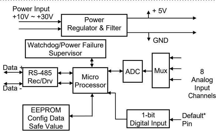
![Based on the provided block diagram, here is the description of the labeled blocks and their connections:\n\n**Power Section:**\n*   **Power Input +10V ~ +30V** connects to **Power Regulator & Filter**.\n*   **Power Regulator & Filter** outputs to **+ 5V** and **GND**.\n\n**Central Processing and Communication:**\n*   The **Micro Processor** is the central block.\n*   **Watchdog/Power Failure Supervisor** connects bidirectionally to the **Micro Processor**.\n*   **RS-485 Rec/Drv** connects bidirectionally to the **Micro Processor**.\n*   **RS-485 Rec/Drv** has connections labeled **Data +** and **Data -** with arrows pointing outward to the left.\n\n**Analog and Digital Inputs:**\n*   **Micro Processor** connects bidirectionally to **ADC**.\n*   **ADC** connects to **Mux**.\n*   **8 Analog Input Channels** provide input to the **Mux** (indicated by arrows pointing left into the Mux).\n*   **1-bit Digital Input** connects to the **Micro Processor** (arrow points up).\n*   **Default* Pin** provides input to the **1-bit Digital Input** (arrow points left).\n\n**Configuration Memory:**\n*   **EEPROM Config Data Safe Value** connects to the **Micro Processor** (arrow points up).](.nudam-6000-50m-00083-1000-31/c99df4958aa205796f62512e314814c49b3322ba2904db3737322db654e88723.jpg)

Figure 3-4 Block Diagram of ND-6017

# 3.3 Overview of ND-6018

ND-6018 is a thermocouple input module with 8 input channels. Six of the eight channels are differential type and the other two are single ended type.

# 3.3.1 Features of ND-6018

. 8 analog input channels
6 differential inputs and 2 single ended inputs
Programmable input voltage range
• Programmable host watchdog timer for host failure protection
. On board CJC for temperature measurement
2500 Vrms isolation voltage
. Internal watchdog timer for device failure protection
• Easy programming by software
• Easy installation and wiring
Wiring open detection

# 3.3.2 Specifications of ND-6018

#  Interface

♦ Interface: RS-485, 2 wires
Speed (bps): 1200, 2400, 4800, 9600, 19.2K, 38.4K , 57.6K, 115.2K

#  Analog Input \*

Input type: Differential input
Channels Numbers: 8
Resolution: 16 bits
Sampling Rate:3 sample/sec
Unit Conversion: Thermocouple, mV, V or mA
Thermocouple Type: J, K, T, E, R, S, B, N, C
♦ J $: 0 ^ { \circ } \mathsf { C } \sim 7 6 0 ^ { \circ } \mathsf { C K } { \mathrm { : } } 0 ^ { \circ } \mathsf { C } \sim 1 3 7 0 ^ { \circ } \mathsf { C }$
♦ $T : - 1 0 0 ^ { \circ } C \sim 4 0 0 ^ { \circ } C \cdot 0 ^ { \circ } C \sim 1 0 0 0 ^ { \circ } C$
♦ R: 500°C\~1750°C S: 500°C\~1750°C
♦ $\mathsf { B } \colon 5 0 0 ^ { \circ } \mathsf { C } \sim 1 8 0 0 ^ { \circ } \mathsf { C } \mathsf { N } \colon - 2 7 0 ^ { \circ } \mathsf { C } \sim 1 3 0 0 ^ { \circ } \mathsf { C }$
♦ C: 0°C\~2320°C
Voltage Range: Programmable 6 levels ±2.5V, ±1V, ±500mV, ±100mV, ±50mV, ±15mV
♦ Current Measurement: 0\~20mA (with external 125∧ resistor)

#  Power

Power supply: +10V to +30V
Current consumption: 0.96 W

Note \*: The maximum input voltage shall not exceed to ±30V with reference to AGND otherwise, they may cause an unrecoverable damage to the hardware component.

3.3.3 A Look at ND-6018 & Pin Assignment
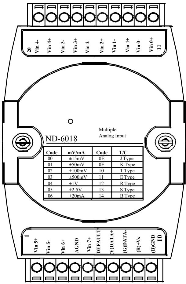
![20 Vin 4- Vin 4+ Vin 3- Vin 3+ Vin 2- Vin 2+ Vin 1- Vin 1+ Vin 0- Vin 0+ 11\nND-6018 Multiple Analog Input\nCode mV/mA Code T/C\n00 ±15mV 0E J Type\n01 ±50mV 0F K Type\n02 ±100mV 10 T Type\n03 ±500mV 11 E Type\n04 ±1V 12 R Type\n05 ±2.5V 13 S Type\n06 ±20mA 14 B Type\n1 Vin 5+ Vin 5- Vin 6+ AGND Vin 7+ DEFAULT Y)DATA+ (G)DATA- (R)+Vs (B)GND 10](.nudam-6000-50m-00083-1000-31/00e29738bd4b53537147133677b1bca1d154de69fe101513a1e2ba67a3116e2f.jpg)

Figure 3-5 ND-6018 profile

3.3.4 Pin Definition of ND-6018

<table><tr><td>Pin #</td><td>Signal Name</td><td>Description</td></tr><tr><td>1</td><td>Vin5+</td><td>Differential positive input channel 5</td></tr><tr><td>2</td><td>Vin5-</td><td>Differential negative input channel 5</td></tr><tr><td>3</td><td>Vin6+</td><td>Single-ended voltage input channel 6</td></tr><tr><td>4</td><td>AGND</td><td>Analog signal ground of CH6 &amp; 7</td></tr><tr><td>5</td><td>Vin7+</td><td>Single-ended voltage input channel 7</td></tr><tr><td>6</td><td>DEFAULT*</td><td>Initial state setting</td></tr><tr><td>7</td><td>(Y) DATA+</td><td>RS-485 series signal, positive</td></tr><tr><td>8</td><td>(G) DATA-</td><td>RS-485 series signal, negative</td></tr><tr><td>9</td><td>(R) +Vs</td><td>Power supply, +10V~+30V</td></tr><tr><td>10</td><td>(B) GND</td><td>Ground</td></tr><tr><td>11</td><td>Vin0+</td><td>Differential positive input channel 0</td></tr><tr><td>12</td><td>Vin0-</td><td>Differential negative input channel 0</td></tr><tr><td>13</td><td>Vin1+</td><td>Differential positive input channel 1</td></tr><tr><td>14</td><td>Vin1-</td><td>Differential negative input channel 1</td></tr><tr><td>15</td><td>Vin2+</td><td>Differential positive input channel 2</td></tr><tr><td>16</td><td>Vin2-</td><td>Differential negative input channel 2</td></tr><tr><td>17</td><td>Vin3+</td><td>Differential positive input channel 3</td></tr><tr><td>18</td><td>Vin3-</td><td>Differential negative input channel 3</td></tr><tr><td>19</td><td>Vin4+</td><td>Differential positive input channel 4</td></tr><tr><td>20</td><td>Vin4-</td><td>Differential negative input channel 4</td></tr></table>

3.3.5 ND-6018 Functional Block Diagram
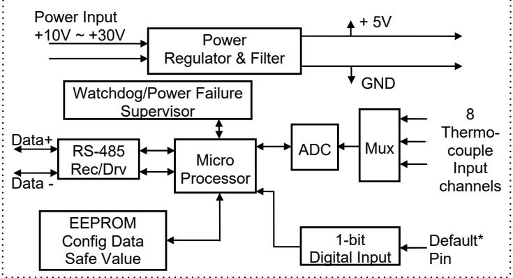
![This block diagram centers around a **Micro Processor** block with the following connections and blocks:\n\n*   **Power Section:** **Power Input +10V ~ +30V** connects to **Power Regulator & Filter**, which outputs **+ 5V** and **GND**.\n*   **Supervision:** **Watchdog/Power Failure Supervisor** connects bidirectionally to the **Micro Processor**.\n*   **Communication:** **RS-485 Rec/Drv** connects bidirectionally to the **Micro Processor** and receives **Data+** and **Data -** inputs.\n*   **Signal Acquisition:** The **Micro Processor** connects bidirectionally to an **ADC**, which connects bidirectionally to a **Mux**. The **Mux** receives inputs from **8 Thermocouple Input channels**.\n*   **Configuration:** **EEPROM Config Data Safe Value** connects bidirectionally to the **Micro Processor**.\n*   **Digital Input:** **Default* Pin** connects to **1-bit Digital Input**, which connects to the **Micro Processor**.](.nudam-6000-50m-00083-1000-31/b4fcfc170e3239011c192063b47a2553d8648022ccf1d751ae3a441f0ce8ed86.jpg)

Figure 3-6 Block Diagram of ND-6018

# 4

# Analog Output Modules

# 4.1 Overview of ND-6021

ND-6021 is an analog signal output module. It receives the digital command from host computer through RS-485 network. The format of the digital value can be engineering units, hexdecimal format or percentage of full-scale range(FSR). A microprocessor is used to convert the digital command to digital value to send to DAC. The DAC converts the digital value into analog form. The analog output can be either voltage or current output.

The ND-6021 is designed for safety. It provides many safety functions such as isolation, watchdog, and power on safe value. The opto-isolators provide 5000Vrms isolation voltage to isolate the digital section and the remote controlled analog equipment. The damage of power surges is avoided.

Another safety function is the watchdog. Whenever the host is loss contact with the remoted NuDAM module, or the micro-processor is down, the module will reset itself and send the safety value to the analog output therefore the industry safety is guarantee. The safety value / power-up value can be set by configuration software.

The analog output can be readback through the module‘s ADC. which can monitor the ’real‘ output of the device. The host can check the digital command and the real output to avoid short circuits. The slew rate of the output signal is also controllable by software.

# 4.1.1 Features of ND-6021

One uni-polar analog output channel
Two sets of differential current and voltage output terminals
Versatile digital signal format
Programmable host watchdog timer for host failure protection
Internal watchdog timer for device failure protection
Easy programming by software
Easy installation and wiring

# 4.1.2 Specifications of ND-6021

#  Interface

Interface : RS-485, 2 wires
Speed (bps) : 1200, 2400, 4800, 9600, 19.2K, 38.4K, 57.6K, 115.2K

#  Analog Output

Singal Output type: Differential type
♦ Resolution: 12 bits
♦ Accuracy: ±0.1% of FSR for currentoutput
Accuracy: ±0.2% of FSR for voltageoutput
Unit Convertion: V or mA
Voltage output range: 0 to 10 V (uni-polar)
Current output range: 0 to 20 mA, 4 to 20 mA
Maximum Sampling Rate: 100 samples /sec
♦ Slew rate of Voltage output: 0.0625 to 64 V/sec
Slew reate of Current output: 0.125 to 128 mA/sec
Internal Current Load Resistor: 500∧ (%1)

#  Isolation

Isolation voltage: 5000 Vrms

#  Watchdog Function

Module internal watchdog timer : 150 ms
+ Power failure threshold : 4.65 V
Host programmable watchdog : 100 ms \~ 25.500 sec

#  Power

Power supply : +10V to +30V
Power consumption : 1.32W

# 4.1.3 A Look at ND-6021 & Pin Assignment
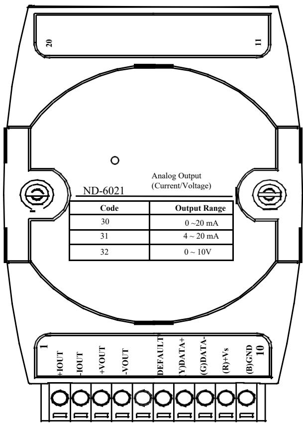
![20\n11\nND-6021 Analog Output\n(Current/Voltage)\nCode	Output Range\n30	0 ~20 mA\n31	4 ~ 20 mA\n32	0 ~ 10V\n+OUT	-IOUT	+VOUT	-VOUT	DEFAULT	Y)DATA+\n(G)DATA-\n(R)+Vs	(B)GND\n10	1](.nudam-6000-50m-00083-1000-31/2e92c194e9533b7d7f385c36d924b89dc08e0419dfc7842b224b6e45dda75a46.jpg)

Figure 4-1 ND-6021 profile

# 4.1.4 Pin Definition of ND-6021

Pin # Signal Name Description

<table><tr><td>1</td><td>+IOUT</td><td>Positive Current Output Terminal</td></tr><tr><td>2</td><td>-IOUT</td><td>Negative Current OutputTerminal</td></tr><tr><td>3</td><td>+VOUT</td><td>Positive Voltage Output Terminal</td></tr><tr><td>4</td><td>-VOUT</td><td>Negative Voltage Output Terminal</td></tr><tr><td>6</td><td>Default*</td><td>Initial state setting</td></tr><tr><td>7</td><td>(Y) DATA+</td><td>RS-485 series signal, positive</td></tr><tr><td>8</td><td>(G) DATA-</td><td>RS-485 series signal, negative</td></tr><tr><td>9</td><td>(R) +Vs</td><td>Power supply, +10V~+30V</td></tr><tr><td>10</td><td>(B) GND</td><td>Ground</td></tr></table>

# 4.1.5 ND-6021 Functional Block Diagram

![Based on the provided block diagram, here is the accurate description of the labeled blocks and their connections:\n\n**Communication and Input Stage**\n*   **RS-485 Rec/DRv**: Connected to external **Data+** and **Data-** lines (which have arrows pointing outward). It is also connected to the **RS-485 Terminator**. It connects bidirectionally to the **Micro Processor**.\n*   **RS-485 Terminator**: Connected to the **Data+** and **Data-** lines.\n\n**Central Processing and Control**\n*   **Micro Processor**: Connects bidirectionally to the **RS-485 Rec/DRv**. It connects bidirectionally to the **Photo Isolators**. It connects bidirectionally to the **EEPROM**. It receives inputs from the **Watchdog / Power Failure Supervisor** and the **\*Defalut Setting (1 bit Digital In)**.\n*   **EEPROM**: Connects bidirectionally to the **Micro Processor**.\n*   **Watchdog / Power Failure Supervisor**: Connects to the **Micro Processor**.\n*   **\*Defalut Setting (1 bit Digital In)**: Connects to the **Micro Processor**.\n\n**Signal Output Stage**\n*   **Photo Isolators**: Connects bidirectionally to the **Micro Processor** and bidirectionally to the **DAC (12 bits)**.\n*   **DAC (12 bits)**: Connects bidirectionally to the **Photo Isolators**. It outputs **VOUT +** and **VOUT -** (labeled **Voltage Output**). It also connects downward to the **V to I** block.\n*   **V to I**: Connects to the **DAC (12 bits)**. It outputs **IOUT +** and **IOUT -** (labeled **Current Output**).\n\n**Power Supply Stage**\n*   **Power Regulator**: Receives input from **+10V ~ +30 V** and **GND**. It outputs **+5V** and **GND** to the **DC to DC Convertor**.\n*   **DC to DC Convertor**: Receives input from the **Power Regulator**. It outputs **Isolated Power** and **Isolated Ground**.](.nudam-6000-50m-00083-1000-31/8ac9129837a69083582aa1bd5677bf5ff8094e61cd2e25155c941b9b6ccbe052.jpg)

Figure 4-2 Block Diagram of ND-6021

# 4.2 Overview of ND-6024

ND-6024 is a 4 channel bipolar analog signal output module. It receives the digital command from host computer through RS-485 network. A microprocessor is used to convert the digital command to digital value to send to DAC. The DAC converts the digital value into analog form.

The ND-6024 is designed for safety. It provides many safety functions such as isolation, watchdog, and power on safe value. The opto-isolators provide 5000Vrms isolation voltage to isolate the digital section and the remotecontrolled analog equipment. The damage of power surges is avoided.

Another safety function is the watchdog. Whenever the host is loss contact with the remoted NuDAM module, or the micro-processor is down, the module will reset itself and send the safety value to the analog output therefore the industry safety is guarantee. The safety value/power-up value can be set by configuration software.

# 4.2.1 Features of ND-6024

4 channel bipolar analog output
Programmable host watchdog timer for host failure protection
Internal watchdog timer for device failure protection
Easy programming by software
Easy installation and wiring

# 4.2.2 Specifications of ND-6024

 Interface

Interface : RS-485, 2 wires
Speed (bps) : 1200, 2400, 4800, 9600, 19.2K, 38.4K, 57.6K, 115.2K

 Analog Output

Channel number : 4
Singal Output type: Differential output

 Voltage Output: ±10V

Resolution: 12 bits resolution
♦ Accuracy: +/-0.02% of FSR(max.)

Digital Input

+ Channel numbers : 7
Switching Level :TTL

 Isolation

♦ Isolation voltage: 5000 Vrms

 Power

Power supply : +10V to +30V
♦ Power consumption : 1.848W

# 4.2.3 A Look at ND-6024 & Pin Assignment

![ND-6024 4-CH\nAnalog Output\nCode Signal\n33 ±10V\nD4 D3 D2 D1 D0 DEFAULT* (V)DATA+ (G)DATA-\n(R)+Vs (B)GND](.nudam-6000-50m-00083-1000-31/fa8ea5f09f9aae027cff4317e1044e6f920455a60840e8d815e85df5fe9b0b10.jpg)

Figure 4-3 ND-6024 profile

4.2.4 Pin Definitions of ND-6024

<table><tr><td>Pin #</td><td>Signal</td><td>Description</td></tr><tr><td>1</td><td>DI4</td><td>Digital input channel 4</td></tr><tr><td>2</td><td>DI3</td><td>Digital input channel 3</td></tr><tr><td>3</td><td>DI2</td><td>Digital input channel 2</td></tr><tr><td>4</td><td>DI1</td><td>Digital input channel 1</td></tr><tr><td>5</td><td>DI0</td><td>Digital input channel 0</td></tr><tr><td>6</td><td>Default*</td><td>Initial state setting</td></tr><tr><td>7</td><td>(Y) DATA+</td><td>RS-485 series signal, positive</td></tr><tr><td>8</td><td>(G) DATA-</td><td>RS-485 series signal, negative</td></tr><tr><td>9</td><td>(R) +Vs</td><td>Power supply, +10V~+30V</td></tr><tr><td>10</td><td>(B) GND</td><td>Ground</td></tr><tr><td>11</td><td>VOUTA+</td><td>Positive Voltage Output A Terminal</td></tr><tr><td>12</td><td>AGND</td><td>Negative Voltage Output A Terminal</td></tr><tr><td>13</td><td>VOUTB+</td><td>Positive Voltage Output B Terminal</td></tr><tr><td>14</td><td>AGND</td><td>Negative Voltage Output B Terminal</td></tr><tr><td>15</td><td>VOUTC+</td><td>Positive Voltage Output C Terminal</td></tr><tr><td>16</td><td>AGND</td><td>Negative Voltage Output C Terminal</td></tr><tr><td>17</td><td>VOUTD+</td><td>Positive Voltage Output D Terminal</td></tr><tr><td>18</td><td>AGND</td><td>Negative Voltage Output D Terminal</td></tr><tr><td>19</td><td>DI6</td><td>Digital input channel 6</td></tr><tr><td>20</td><td>DI5</td><td>Digital input channel 5</td></tr></table>

# 4.2.5 ND-6024 Functional Block Diagram

![Based on the provided block diagram, here is an accurate and concise description of the blocks and their connections:\n\n**System Components:**\n*   **RS-485 Rec/DRv**\n*   **RS-485 Terminator**\n*   **Micro Processor**\n*   **Photo Isolators**\n*   **DAC (12 bits)**\n*   **EEPROM**\n*   **Watchdog / Power Failure Supervisor**\n*   ***Default Setting (1 bit Digital In)**\n*   **DI0...... DI6**\n*   **Voltage Output**\n*   **Power Regulator**\n*   **DC to DC Convertor**\n\n**Connections and Data Flow:**\n\n*   **Data Interface:** **Data+** and **Data-** arrows connect to the **RS-485 Rec/DRv** block. The **RS-485 Terminator** block is connected to the **Data+** and **Data-** lines. The **RS-485 Rec/DRv** connects bidirectionally to the **Micro Processor**.\n*   **Processing & Output:** The **Micro Processor** connects to **Photo Isolators**, which feed into the **DAC (12 bits)**. The DAC outputs to the **Voltage Output** block, which contains the following list:\n    *   **•VOUTA+**\n    *   **AGND**\n    *   **•VOUTB+**\n    *   **AGND**\n    *   **•VOUTC+**\n    *   **AGND**\n    *   **•VOUTD+**\n    *   **AGND**\n*   **Micro Processor Inputs/Outputs:** The **Micro Processor** connects to the **EEPROM**, **Watchdog / Power Failure Supervisor**, ***Default Setting (1 bit Digital In)**, and **DI0...... DI6**.\n*   **Power Supply:** **+10V ~ +30 V** and **GND** connect to the **Power Regulator**. The regulator outputs **+5V** and **GND** into the **DC to DC Convertor**. The converter outputs **Isolated Power** and **Isolated Ground**.](.nudam-6000-50m-00083-1000-31/e7aa0adc1077e90a7de5b4b778310621ea519ba3fc06bf143f9c7d0f943b94ef.jpg)

Figure 4-4 Block Diagram of ND-6024

# 5

# Digital I/O Modules

# About the NuDAM DIO Modules

The NuDAM provides a series of digital input or output (DIO) modules to sense the digital signal or to control the remote devices.

The specified features of each module are shown here.

ND-6050 : Digital I/O module
ND-6052 : Isolated digital input module
ND-6053 : 16-channel digital input module
ND-6054 : 15-channel isolated digital input module
ND-6056 : 15-channel isolated digital output module
ND-6058 : 28 programmable digital I/O module
ND-6060 : relay output and isolated digital input module
ND-6063 : 8-channel relay output module
ND-6067 : 8-channel AC relay output module

# 5.1 Overview of ND-6050

ND-6050 is a digital input and output module. The digital input channels can monitor active TTL signals, and sense passive switch on/off signal because of the internal pull high resistors. The convenient open collector output channels can sink up to 50 mA current. Combining with the relay devices, it is possible to control the high power devices by programming output channel of the ND-6050.

# 5.1.1 Features of ND-6050

7 channels digital input
8 channels open collector digital output
Programmable host watchdog timer for host failure protection
Internal watchdog timer for device failure protection
Easy programming by software
Easy installation and wiring

# 5.1.2 Specifications of ND-6050

#  Interface

Interface : RS-485, 2 wires
Speed (bps) : 1200, 2400, 4800, 9600, 19.2K, 38.4K, 57.6K, 115.2K

#  Digital Input

♦ Channel numbers : 7
Switching Level :TTL
♦ Pull up resister : 10K∧
♦ Maximum current : 0.5mA

#  Digital Output

♦ Channel number : 8
Output characteristic : open collector transistor
♦ Maximum current sink : 50mA
♦ Max. power dissipation : 300mW

#  Watchdog Function

Module internal watchdog timer: 150 ms
♦ Power failure threshold : 4.65 V
Safety value : 8 output channels
♦ Host programmable watchdog :
+ 100 ms \~ 25.500 sec

#  Power

Power supply : +10V to +30V
♦ Current consumption : 0.336W

5.1.3 A Look at ND-6050 & Pin Assignment
![20\nDI 6\nDI 5\nDI 4\nDI 3\nDI 2\nDI 1\nDI 0\nDO 0\nDO 1\nDO 2\n11\nDigital\nInput/Output\nND-6050\nI/O Type\nSignal\nDigital Output\nBit 0-7\nDigital Input\nBit 0-6\n1\nDO 7\nDO 6\nDO 5\nDO 4\nDO 3\nDEFAULT\nY)DATA+\n(G)DATA-\n(R)+Vs\n(B)GND\n10](.nudam-6000-50m-00083-1000-31/e7e26f66a0fbaeb9b9b1cc488fdf8d73e1c2b45802f0e72f06c303e1e69a885d.jpg)

Figure 5-1 ND-6050 profile

5.1.4 Pin Definitions of ND-6050

<table><tr><td>Pin #</td><td>Signal Name</td><td>Description</td></tr><tr><td>1</td><td>DO 7</td><td>Digital output channel 7</td></tr><tr><td>2</td><td>DO 6</td><td>Digital output channel 6</td></tr><tr><td>3</td><td>DO 5</td><td>Digital output channel 5</td></tr><tr><td>4</td><td>DO 4</td><td>Digital output channel 4</td></tr><tr><td>5</td><td>DO 3</td><td>Digital output channel 3</td></tr><tr><td>6</td><td>Default*</td><td>Initial state setting</td></tr><tr><td>7</td><td>(Y) DATA+</td><td>RS-485 series signal, positive</td></tr><tr><td>8</td><td>(G) DATA-</td><td>RS-485 series signal, negative</td></tr><tr><td>9</td><td>(R) +Vs</td><td>Power supply, +10V~+30V</td></tr><tr><td>10</td><td>(B) GND</td><td>Ground</td></tr><tr><td>11</td><td>DO 2</td><td>Digital output channel 2</td></tr><tr><td>12</td><td>DO 1</td><td>Digital output channel 1</td></tr><tr><td>13</td><td>DO 0</td><td>Digital output channel 0</td></tr><tr><td>14</td><td>DI 0</td><td>Digital input channel 0</td></tr><tr><td>15</td><td>DI 1</td><td>Digital input channel 1</td></tr><tr><td>16</td><td>DI 2</td><td>Digital input channel 2</td></tr><tr><td>17</td><td>DI 3</td><td>Digital input channel 3</td></tr><tr><td>18</td><td>DI 4</td><td>Digital input channel 4</td></tr><tr><td>19</td><td>DI 5</td><td>Digital input channel 5</td></tr><tr><td>20</td><td>DI 6</td><td>Digital input channel 6</td></tr></table>

5.1.5 ND-6050 Functional Block Diagram
![Based on the provided block diagram, here are the labeled blocks and their connections:\n\n**Labeled Blocks:**\n*   Power Regulator & Filter\n*   Watchdog/Power Failure Supervisor\n*   RS-485 Rec/Drv\n*   Micro Processor\n*   EEPROM Config Data Safe Value\n*   8-bit Digital/Output\n*   7-bit Digital/Input\n*   1-bit Digital/Input\n\n**Connections:**\n*   **Power Input +10V ~ +30V** points to **Power Regulator & Filter**.\n*   **Power Regulator & Filter** outputs **+ 5V** (upward arrow) and **GND** (rightward arrow), and connects to **8-bit Digital/Output**.\n*   **Watchdog/Power Failure Supervisor** points to **Micro Processor**.\n*   **RS-485 Rec/Drv** has bidirectional connections with **Micro Processor** and outputs **Data +** and **Data -** (leftward arrows).\n*   **Micro Processor** has bidirectional connections with **8-bit Digital/Output**, **7-bit Digital/Input**, and **1-bit Digital/Input**. It also points to **EEPROM Config Data Safe Value**.\n*   **8-bit Digital/Output** outputs **DO0** and **DO7** (rightward arrows).\n*   **7-bit Digital/Input** receives **DI0** and **DI6** (leftward arrows).\n*   **1-bit Digital/Input** receives **Default* Pin** (leftward arrow).](.nudam-6000-50m-00083-1000-31/979d293f3219a4b3d08351d57661f65e0e383aba970107d8384b90d2512935ba.jpg)

Figure 5-2 Block Diagram of ND-6050

# 5.2 Overview of ND-6052

ND-6052 provides 8 isolated digital input channels. Six of the input channels are differential type and two of them are single-ended with common ground. The isolation voltage is up to 5000 Vrms. It is suitable to use ND-6052 in industrial environment with high voltage electric shock.

# 5.2.1 Features of ND-6052

8 bits isolated input
5000 Vrms isolation voltage
Programmable host watchdog timer for host failure protection
Internal watchdog timer for device failure protection
Easy programming by software
Easy installation and wiring

# 5.2.2 Specifications of ND-6052

#  Interface

Interface : RS-485, 2 wires
Speed (bps) : 1200, 2400, 4800, 9600, 19.2K, 38.4K, 57.6K, 115.2K

#  Input

Channel number : 6 differential channels, 2 single ended
Logical level 0 : +1V Max.
Logical level 1: +3.5V \~ +24V

#  Watchdog Function

Module internal watchdog timer : 150ms
Power failure threshold : 4.65 V
Safe value : 8 output channels
Host programmable watchdog :100 ms \~ 25.5 sec

#  Power

Power supply : +10V to +30V
Current consumption : 0.264 W

5.2.3 A Look at ND-6052 & Pin Assignment
![20\nDI 4-\nDI 4+\nDI 3-\nDI 3+\nDI 2-\nDI 2+\nDI 1-\nDI 1+\nDI 0-\nDI 0+\n11\nND-6052 Isolated\nDigital Input\nInput Type Channels\nDifferential 6\nSingle Ended 2\n1\nDI 5+\nDI 5-\nDI 6+\nD.GND\nDI 7+\nDEFAULT Y)DATA+\n(G)DATA-\n(R)+Vs\n(B)GND 10](.nudam-6000-50m-00083-1000-31/039930e679fed06e333ab1803b2f90134980285a7be797e2395134c537de4502.jpg)

Figure 5-3 ND-6052 profile

5.2.4 Pin Definitions of ND-6052

<table><tr><td>Pin #</td><td>Signal Name</td><td>Description</td></tr><tr><td>1</td><td>DI5+</td><td>Digital Input Channel 5+</td></tr><tr><td>2</td><td>DI5 -</td><td>Digital Input Channel 5 -</td></tr><tr><td>3</td><td>DI6+</td><td>Digital Input Channel 6+</td></tr><tr><td>4</td><td>D.GND</td><td>Digital Input Ground</td></tr><tr><td>5</td><td>DI7+</td><td>Digital Input Channel 7+</td></tr><tr><td>6</td><td>Default*</td><td>Initial state setting</td></tr><tr><td>7</td><td>(Y) DATA+</td><td>RS-485 series signal, positive</td></tr><tr><td>8</td><td>(G) DATA-</td><td>RS-485 series signal, negative</td></tr><tr><td>9</td><td>(R) +VS</td><td>Power supply, +10V~+30V</td></tr><tr><td>10</td><td>(B) GND</td><td>Ground</td></tr><tr><td>11</td><td>DI0+</td><td>Digital Input Channel 0+</td></tr><tr><td>12</td><td>DI0 -</td><td>Digital Input Channel 0 -</td></tr><tr><td>13</td><td>DI1+</td><td>Digital Input Channel 1+</td></tr><tr><td>14</td><td>DI1 -</td><td>Digital Input Channel 1 -</td></tr><tr><td>15</td><td>DI2+</td><td>Digital Input Channel 2+</td></tr><tr><td>16</td><td>DI2 -</td><td>Digital Input Channel 2 -</td></tr><tr><td>17</td><td>DI3+</td><td>Digital Input Channel 3+</td></tr><tr><td>18</td><td>DI3 -</td><td>Digital Input Channel 3 -</td></tr><tr><td>19</td><td>DI4+</td><td>Digital Input Channel 4+</td></tr><tr><td>20</td><td>DI4 -</td><td>Digital Input Channel 4 -</td></tr></table>

5.2.5 ND-6052 Functional Block Diagram
![The flowchart depicts a system block diagram, likely for a communication or control module. Here is the accurate description of the blocks and connections:\n\n**Power Section**\n*   **Block:** 'Power Input +10V ~ +30V' (inputs two lines).\n*   **Connection:** Arrows point from the power input into the **'Power Regulator & Filter'** block.\n*   **Block:** 'Power Regulator & Filter'.\n*   **Connection:** An arrow points up to **'+5V'**. An arrow points right to **'GND'**.\n\n**Central Processing Section**\n*   **Block:** 'Watchdog/Power Failure Supervisor'.\n*   **Connection:** An arrow points down from this block to the central **'Micro Processor'**.\n*   **Block:** 'EEPROM Config Data Safe Value'.\n*   **Connection:** An arrow points up from this block to the **'Micro Processor'**.\n*   **Block:** 'RS-485 Rec/Drv'.\n*   **Connection:** Bidirectional arrows connect this block to the **'Micro Processor'**.\n*   **Connection:** Arrows point left from 'RS-485 Rec/Drv' to labels **'Data +'** and **'Data -'**.\n\n**Digital Input Section (Right Side)**\n*   **Block:** 'Micro Processor' (Central Hub).\n*   **Connection:** An arrow points left from a dotted box (labeled **'DI0+'** and **'DI0-'**) to the **'Micro Processor'**.\n    *   *Note:* Above this area is a circuit diagram showing a resistor connecting to **'+5V'**, capacitors, and diodes, leading to labels **'DI0+'** and **'DI0-'**.\n*   **Connection:** A dotted line connects the **'DI0+' / 'DI0-'** box down to a box labeled **'DI5+'** and **'DI5-'**.\n*   **Connection:** Lines connect the **'Micro Processor'** to three stacked boxes at the bottom right:\n    1.  A box labeled **'DI5+'** and **'DI5-'**.\n    2.  A box labeled **'DI6+'** and **'D.GND'**.\n    3.  A box labeled **'DI7+'** and **'D.GND'**.](.nudam-6000-50m-00083-1000-31/f1e35d57101d3175ca1bc7d89bf378a132cbd7d8727f4b6ae787f59b6f075446.jpg)

Figure 5-4 Block Diagram of ND-6052

# 5.3 Overview of ND-6053

ND-6053 provides 16 digital input channels for dry contact or wet contact signals. The effective distance from DI to contact point is up to 500 meter for dry contact input.

# 5.3.1 Features of ND-6053

16 bits digital input
Programmable host watchdog timer for host failure protection
Internal watchdog timer for device failure protection
Easy programming by software
Easy installation and wiring

# 5.3.2 Specifications of ND-6053

#  Interface

Interface : RS-485, 2 wires
Speed (bps) : 1200, 2400, 4800, 9600, 19.2K, 38.4K, 57.6K, 115.2K

#  Input

+ Channel numbers : 16
Dry Contact:
Logical level 0 : close to GND
Logical level 1 : open
+ Wet Contact :
Switching Level :TTL
♦ Maximum current sink : 50mA

#  Watchdog Function

Module internal watchdog timer : 150ms
♦ Power failure threshold : 4.65 V
Host programmable watchdog : 100 ms \~ 25.5 sec

#  Power

♦ Power supply : +10V to +30V
Current consumption : 0.408 W

5.3.3 A Look at ND-6053 & Pin Assignment
![20\nD19 D18 D17 D16 D15 D14 D13 D12 D11 D10\nND-6053 16-CH Digital\nInput Type Channels\nDigital Input 16\n1\nD110 D111 D112 D113 D114 DEFAULT (V)DATA+\n(G)DATA-\n(R)+Vs (B)GND 10](.nudam-6000-50m-00083-1000-31/2c5abda8f5bcb9ec6cedda8029a414541af116ed74b0345b44f91bfc3783507c.jpg)

Figure 5-5 ND-6053 profile

5.3.4 Pin Definitions of ND-6053

<table><tr><td>Pin #</td><td>Signal Name</td><td>Description</td></tr><tr><td>1</td><td>DI10</td><td>Digital Input Channel 10</td></tr><tr><td>2</td><td>DI11</td><td>Digital Input Channel 11</td></tr><tr><td>3</td><td>DI12</td><td>Digital Input Channel 12</td></tr><tr><td>4</td><td>DI13</td><td>Digital Input Channel 13</td></tr><tr><td>5</td><td>DI14</td><td>Digital Input Channel 14</td></tr><tr><td>6</td><td>Default*/DI15</td><td>Initial state setting/ Digital Input Channel 15</td></tr><tr><td>7</td><td>(Y) DATA+</td><td>RS-485 series signal, positive</td></tr><tr><td>8</td><td>(G) DATA-</td><td>RS-485 series signal, negative</td></tr><tr><td>9</td><td>(R) +VS</td><td>Power supply, +10V~+30V</td></tr><tr><td>10</td><td>(B) GND</td><td>Ground</td></tr><tr><td>11</td><td>DI0</td><td>Digital Input Channel 0</td></tr><tr><td>12</td><td>DI1</td><td>Digital Input Channel 1</td></tr><tr><td>13</td><td>DI2</td><td>Digital Input Channel 2</td></tr><tr><td>14</td><td>DI3</td><td>Digital Input Channel 3</td></tr><tr><td>15</td><td>DI4</td><td>Digital Input Channel 4</td></tr><tr><td>16</td><td>DI5</td><td>Digital Input Channel 5</td></tr><tr><td>17</td><td>DI6</td><td>Digital Input Channel 6</td></tr><tr><td>18</td><td>DI7</td><td>Digital Input Channel 7</td></tr><tr><td>19</td><td>DI8</td><td>Digital Input Channel 8</td></tr><tr><td>20</td><td>DI9</td><td>Digital Input Channel 9</td></tr></table>

# 5.3.5 ND-6053 Functional Block Diagram

![Based on the provided block diagram, here are the labeled blocks and their connections:\n\n**Labeled Blocks:**\n*   Power Regulator & Filter\n*   Watchdog/Power Failure Supervisor\n*   Micro Processor\n*   RS-485 Rec/Drv\n*   EEPROM Config Data Safe Value\n*   15-bit Digital/Input\n*   1-bit Digital/Input\n\n**Connections:**\n*   **Power Input +10V ~ +30V** connects to the **Power Regulator & Filter**.\n*   The **Power Regulator & Filter** outputs **+ 5V** and **GND**.\n*   The **Micro Processor** connects bidirectionally to the **Watchdog/Power Failure Supervisor**.\n*   The **Micro Processor** connects bidirectionally to the **RS-485 Rec/Drv**.\n*   The **RS-485 Rec/Drv** outputs **Data +** and **Data -**.\n*   The **Micro Processor** connects bidirectionally to the **15-bit Digital/Input**.\n*   The **15-bit Digital/Input** receives inputs from **DI0** and **DI14**.\n*   The **Micro Processor** connects unidirectionally (output) to the **1-bit Digital/Input**.\n*   The **1-bit Digital/Input** receives an input from **Default* Pin/DI15**.\n*   The **Micro Processor** connects unidirectionally (output) to the **EEPROM Config Data Safe Value**.](.nudam-6000-50m-00083-1000-31/8cd23c8d4bb8497742178e463c72c10358a5fe89a0ed9aa0eab447690280e8c1.jpg)

Figure 5-6 Block Diagram of ND-6053

# 5.4 Overview of ND-6054

ND-6054 provides 15 isolated digital input channels. All of the input channels are common power type and one of them is using the same pin with default (use jumper to choose). The isolation voltage is up to 5000 Vrms. It is suitable to use ND-6054 in industrial environment with high voltage electric shock.

# 5.4.1 Features of ND-6054

15 channels digital inputs with isolation protection and common power
5000 Vrms isolation voltage
Programmable host watchdog timer for host failure protection
Internal watchdog timer for device failure protection
Easy programming by software
Easy installation and wiring

# 5.4.2 Specifications of ND-6054

#  Interface

Interface : RS-485, 2 wires
Speed (bps) : 1200, 2400, 4800, 9600, 19.2K, 38.4K, 57.6K, 115.2K

#  Input

Channel numbers : 15 isolation common power input channels (the fifteenth channel is the same with default pin, but can use jumper to choose)
Logical level 0 : +1V Max.
Logical level $1 { \mathrm { : } } + 3 . 5 \mathsf { V } \sim + 2 4 \mathsf { V }$
♦ Effective distance: 500 meter
♦ Common external voltage: 24V

#  Watchdog Function

Module internal watchdog timer : 150msec
+ Power failure threshold : 4.65 V
Host programmable watchdog :100 ms \~ 25.5 sec

#  Power

Power supply : +10V to +30V
♦ Power consumption : 0.216 W

# 5.4.3 A Look at ND-6054 & Pin Assignment

![20\nDI0 DI1 DI2 DI3 DI4 DI5 DI6 DI7 DI8 DI9\n15-CH Isolated\nDigital Input\nND-6054\nInput Type Channels\nDI 15\n1 DI10 DI11 DI12 DI13 Ext24V DEFAULT*\nDI14 Y)DATA+\n(G)DATA-\n(R)+Vs (BGND)](.nudam-6000-50m-00083-1000-31/fab1ee4b3c3ba74f4cb26cdd5c287e86b40e44c31a516536aa4155334ed79c52.jpg)

Figure 5-7 ND-6054 profile

5.4.4 Pin Definitions of ND-6054

<table><tr><td>Pin #</td><td>Signal Name</td><td>Description</td></tr><tr><td>1</td><td>DI10</td><td>Digital input channel 10</td></tr><tr><td>2</td><td>DI11</td><td>Digital input channel 11</td></tr><tr><td>3</td><td>DI12</td><td>Digital input channel 12</td></tr><tr><td>4</td><td>DI13</td><td>Digital input channel 13</td></tr><tr><td>5</td><td>Ext24V</td><td>External common +24V</td></tr><tr><td>6</td><td>Default*/DI14</td><td>Initial state setting or digital input channel 14</td></tr><tr><td>7</td><td>(Y) DATA+</td><td>RS-485 series signal, positive</td></tr><tr><td>8</td><td>(G) DATA-</td><td>RS-485 series signal, negative</td></tr><tr><td>9</td><td>(R) +VS</td><td>Power supply, +10V~+30V</td></tr><tr><td>10</td><td>(B) GND</td><td>Ground</td></tr><tr><td>11</td><td>DI9</td><td>Digital input channel 9</td></tr><tr><td>12</td><td>DI8</td><td>Digital input channel 8</td></tr><tr><td>13</td><td>DI7</td><td>Digital input channel 7</td></tr><tr><td>14</td><td>DI6</td><td>Digital input channel 6</td></tr><tr><td>15</td><td>DI5</td><td>Digital input channel 5</td></tr><tr><td>16</td><td>DI4</td><td>Digital input channel 4</td></tr><tr><td>17</td><td>DI3</td><td>Digital input channel 3</td></tr><tr><td>18</td><td>DI2</td><td>Digital input channel 2</td></tr><tr><td>19</td><td>DI1</td><td>Digital input channel 1</td></tr><tr><td>20</td><td>DI0</td><td>Digital input channel 0</td></tr></table>

5.4.5 ND-6054 Functional Block Diagram
![Based on the provided flowchart/block diagram, here is the accurate and concise description:\n\n**Labeled Blocks:**\n*   Power Regulator & Filter\n*   Watchdog/Power Failure Supervisor\n*   Micro Processor\n*   RS-485 Rec/Drv\n*   EEPROM Config Data Safe Value\n\n**Connections and Flow:**\n*   **Power Input:** Two lines labeled 'Power Input +10V ~ +30V' connect to the 'Power Regulator & Filter'.\n*   **Regulator Outputs:** From the 'Power Regulator & Filter', an arrow points up to '+5V' and an arrow points right to 'GND'. A line labeled '+5V' extends downward from the regulator area.\n*   **Micro Processor Connections:**\n    *   The downward '+5V' line connects to the 'Micro Processor'.\n    *   A double-headed arrow connects the 'Micro Processor' to the 'Watchdog/Power Failure Supervisor'.\n    *   Double-headed arrows connect the 'Micro Processor' to the 'RS-485 Rec/Drv'.\n    *   A double-headed arrow connects the 'Micro Processor' to the 'EEPROM Config Data Safe Value'.\n    *   Lines extend from the right side of the 'Micro Processor' to four dotted rectangular blocks.\n*   **RS-485 Outputs:** Two arrows point left from the 'RS-485 Rec/Drv' block, labeled 'Data +' and 'Data -'.\n*   **DI0 Input Circuit:** A resistor (zig-zag symbol) connects the '+5V' rail to a protection circuit (containing diodes and capacitors). This circuit has outputs labeled '+24V' and 'DI0'.\n*   **Digital Inputs (DI1, DI12, DI13, DI14):** The lines from the 'Micro Processor' connect to the four dotted blocks on the right. Each block has outputs labeled '+24V' and a specific input label:\n    *   DI1\n    *   DI12\n    *   DI13\n    *   DI14](.nudam-6000-50m-00083-1000-31/26d54a1a97255a2a83d9ede8a28b9d3b6cd5db9633de49fb178a79679934ec86.jpg)

Figure 5-8 Block Diagram of ND-6054

# 5.5 Overview of NuDAM-6056

# What is NuDAM-6056 ?

NuDAM-6056 provides 15 isolated digital output channels. All of the output channels are common ground type and one of them is use the same pin with default (use jumper to choose). The isolation voltage is up to 5000 Vrms. It is suitable to use NuDAM-6056 in industrial environment with high voltage electric shock.

# 5.5.1 Features of NuDAM-6056

15 bits digital open collector output with isolation protection and common ground
5000 Vrms isolation voltage
Programmable host watchdog timer for host failure protection
Internal watchdog timer for device failure protection
Easy programming by software
Easy installation and wiring

# 5.5.2 Specifications of NuDAM-6056

# Interface

Interface : RS-485, 2 wires
Speed (bps) : 1200, 2400, 4800, 9600, 19.2K, 38.4K, 57.6K, 115.2K (115.2K is only for firmware reversion above A4.00)

#  Digital Output

Channel numbers : 15 isolation common ground output channels(the fifteenth channel is the same with default pin,but could use jumper to choose).
♦ Output characteristic:open collector transistor
♦ Maximum current sink:50mA(300mA for Hardware Reversion.A2)
Max.power dissiation:200mW(3W for Hardware Reversion.A2)
Isolation Voltage:5000Vrms

#  Watchdog Function

Module internal watchdog timer : 150msec
▲ Power failure threshold : 4.65V
Safe value : 15 output channels
Host programmable watchdog :100 ms \~ 25.5 sec

#  Power

Power supply : +10V to +30V
Current consumption :1.32W

# 5.5.3 A Look at NuDAM-6056 & Pin Assignment

![15-CH Isolated\nDigital Output\nND-6056\nOutput Type	Channels\nDO	15\n1	DO10	DO11	DO12	DO13	Ext.GND	DEFAULT	Y)DATA+	(G)DATA-\n	(R)+Vs	(B)GND](.nudam-6000-50m-00083-1000-31/49724f5173896ba3c5647fede7b50d686544aca707f0eb8a64f27755a468292c.jpg)

Figure 5-9 NuDAM-6056 profile

# 5.5.4 Pin Definitions of NuDAM-6056

<table><tr><td>Pin #</td><td>Signal Name</td><td>Description</td></tr><tr><td>1</td><td>DO10</td><td>Digital output channel 10</td></tr><tr><td>2</td><td>DO11</td><td>Digital output channel 11</td></tr><tr><td>3</td><td>DO12</td><td>Digital output channel 12</td></tr><tr><td>4</td><td>DO13</td><td>Digital output channel 13</td></tr><tr><td>5</td><td>ExtGND</td><td>External Ground</td></tr><tr><td>6</td><td>Default*/DO14</td><td>Initial state setting or Digital output channel 14</td></tr><tr><td>7</td><td>(Y) DATA+</td><td>RS-485 series signal, positive</td></tr><tr><td>8</td><td>(G) DATA-</td><td>RS-485 series signal, negative</td></tr><tr><td>9</td><td>(R) +VS</td><td>Power supply, +10V~+30V</td></tr><tr><td>10</td><td>(B) GND</td><td>Ground</td></tr><tr><td>11</td><td>DO0</td><td>Digital output channel 0</td></tr><tr><td>12</td><td>DO1</td><td>Digital output channel 1</td></tr><tr><td>13</td><td>DO2</td><td>Digital output channel 2</td></tr><tr><td>14</td><td>DO3</td><td>Digital output channel 3</td></tr><tr><td>15</td><td>DO4</td><td>Digital output channel 4</td></tr><tr><td>16</td><td>DO5</td><td>Digital output channel 5</td></tr><tr><td>17</td><td>DO6</td><td>Digital output channel 6</td></tr><tr><td>18</td><td>DO7</td><td>Digital output channel 7</td></tr><tr><td>19</td><td>DO8</td><td>Digital output channel 8</td></tr><tr><td>20</td><td>DO9</td><td>Digital output channel 9</td></tr></table>

# 5.5.5 NuDAM-6056 Functional Block Diagram

![Based on the provided block diagram, here is the accurate and concise description of the labeled blocks and their connections:\n\n**Blocks:**\n*   Power Regulator & Filter\n*   Watchdog/Power Failure Supervisor\n*   RS-485 Rec/Drv\n*   Micro Processor\n*   EEPROM Config Data Safe Value\n*   Output Driver placeholders (represented by dotted boxes connected to DO0, DO1, DO12, DO13, and DO14)\n\n**Connections:**\n*   **Power Input +10V** connects to the **Power Regulator & Filter**.\n*   The **Power Regulator & Filter** outputs **+5V** and **GND**.\n*   The **Watchdog/Power Failure Supervisor** connects bidirectionally (double arrow) to the **Micro Processor**.\n*   The **RS-485 Rec/Drv** connects bidirectionally (double arrow) to the **Micro Processor**.\n*   The **RS-485 Rec/Drv** has outputs labeled **Data +** and **Data -** (arrows point left).\n*   The **Micro Processor** connects to the **EEPROM Config Data Safe Value** (arrow points from Micro Processor to EEPROM).\n*   The **Micro Processor** connects to a circuit (dotted box containing a diode and transistor) that outputs **DO0** and **COM**. This circuit is pulled up to **+V**.\n*   A dotted box labeled **DO1** and **COM** connects to the **Micro Processor** (arrow points from the box to the Micro Processor).\n*   The **Micro Processor** connects to dotted boxes labeled **DO12** and **COM**, **DO13** and **COM**, and **DO14** and **COM** (lines originate from the bottom of the Micro Processor).](.nudam-6000-50m-00083-1000-31/a79c1b50c23cbdd2d0397fad645b1c94a8222d016d684c2e74f55f89a6a7e9ad.jpg)

Figure 5-10 Block Diagram of NuDAM-6056

# 5.6 Overview of NuDAM-6058

# What is NuDAM-6058 ?

NuDAM-6058 provides 28 digital I/O channels. It emulates industry standard mode zero configuration of 8255 programmable peripheral interface (PPI) chip. The PPI offers 3 ports A, B and C, the C port can also be subdivided into 2 nibble-wide (4-bit) port – C upper and C lower. A 50 pin SCSI connector equipped with ND-6058 which is corresponding to PPI chip with 24 DIO points.

# 5.6.1 Features of NuDAM-6058

Industry standard 8255 programmable peripheral interface mode 0 emulation
24 Programmable I/O channels
4 dedicated input channels
Completely TTL compatible I/O lines
Status read-back capability
Direct bit set/reset capability
Buffered circuits for higher driving capability
Direct interface with OPTO-22 compatible I/O module
Programmable host watchdog timer for host failure protection
Internal watchdog timer for device failure protection
On board resetable fuse to protect power supply form external devices
Easy programming by software
Easy installation and wiring

# 5.6.2 Specifications of NuDAM-6058

#  Interface

♦ Interface : RS-485, 2 wires
Speed (bps) : 1200, 2400, 4800, 9600, 19.2K, 38.4K, 57.6K, 115.2K (115.2K is only for firmware reversion above A4.00)

#  Programmable Digital Input/Output

♦ Channel numbers : 24
+ Input Signal:
Logical level 0: 0.8 Vmax
♦ Logical level 1: 2.0 Vmin.
Output Signal:
Logical level 0: 0.5 Vmax.
Logical level 1: 2.4 Vmin.

#  Watchdog Function

Module internal watchdog timer : 150msec
♦ Power failure threshold : 4.65V
Safe value : 15 output channels
Host programmable watchdog :100 ms \~ 25.5 sec

#  Dedicated Digital Input

♦ Channel numbers : 4
♦ Input Signal:
Logical level 0: -0.5\~0 V
♦ Logical level 1: 3 V \~ 5.25 V

#  Connector

♦ 10-pin skew terminal block
50-pin SCSI II connector

#  Power

Power supply : +10V to +30V
♦ Current consumption: 1.488 W

# 5.6.3 A Look at NuDAM-6058 & Pin Assignment

![A0 ~ A7 B0 ~ B7 C0 ~ C7 50\nND-6058\n28-CH Programmable\nDigital I/O\nType Channels\nPPI 24\nDI 4\n1 D10 D11 D12 D13 DEFAULT * (Y)DATA+ (G)DATA- (R)+Vs (B)GND 10](.nudam-6000-50m-00083-1000-31/383ba0c7543c481741aaecb3cbf0717942c75c98b4f7a1a2bd44bd7ebc858600.jpg)

Figure 5-11 NuDAM-6058 profile

5.6.4 Pin Definitions of NuDAM-6058

<table><tr><td>Pin #</td><td>Signal Name</td><td>Description</td></tr><tr><td>1</td><td>DI0</td><td>Digital input channel 0</td></tr><tr><td>2</td><td>DI1</td><td>Digital input channel 1</td></tr><tr><td>3</td><td>DI2</td><td>Digital input channel 2</td></tr><tr><td>4</td><td>DI3</td><td>Digital input channel 3</td></tr><tr><td>5</td><td></td><td></td></tr><tr><td>6</td><td>Default*</td><td>Initial state setting</td></tr><tr><td>7</td><td>(Y) DATA+</td><td>RS-485 series signal, positive</td></tr><tr><td>8</td><td>(G) DATA-</td><td>RS-485 series signal, negative</td></tr><tr><td>9</td><td>(R) +VS</td><td>Power supply, +10V~+30V</td></tr><tr><td>10</td><td>(B) GND</td><td>Ground</td></tr></table>

![A0\n1\n2\n3\n4\n5\n6\n7\n8\n9\nB0\n10\n11\n12\n13\n14\n15\n16\n17\nC0\n18\n19\n20\n21\n22\n23\n24\n25\n+5V\nFuse\n26\n27\n28\n29\n30\n31\n32\n33\n34\n35\n36\n37\n38\n39\n40\n41\n42\n43\n44\n45\n46\n47\n48\n49\n50\n+Vs\nFuse\n50Pin SCSI](.nudam-6000-50m-00083-1000-31/48ffb100ca9bcead593e47606cac338b6acc84018f021b5285549f4b70d11aa8.jpg)

5.6.5 NuDAM-6058 Functional Block Diagram
![This block diagram illustrates a power supply and a microprocessor-based control system.\n\n**Power Section**\n*   **Power Input +10V ~ +30V**: Two lines enter the left side of the **Power Regulator & Filter** block.\n*   **Power Regulator & Filter**: Outputs **+5V** (via an upward arrow) and **GND** (via an upward arrow) on the right side.\n\n**Microprocessor Section**\nA central **Micro Processor** block connects to several peripherals:\n*   **Watchdog/Power Failure Supervisor**: Connected via a vertical bidirectional arrow.\n*   **RS-485 Rec/Drv**: Connected via a horizontal bidirectional arrow. This block outputs **Data +** and **Data -** (arrows pointing left).\n*   **EEPROM Config Data Safe Value**: Connected via an arrow pointing from the Micro Processor to the EEPROM block.\n*   **DI0 ... ... DI3**: Connected via an arrow pointing from the label into the Micro Processor.\n*   **Unlabelled Rectangular Block**: Connected via an arrow pointing from this block into the Micro Processor. This block interfaces with external lines labeled **A0~A7**, **B0~B7**, and **C0~C7**.](.nudam-6000-50m-00083-1000-31/fe88d25e48d7d27708150453582866525778a0af67f204e7f2737a24a5dbce27.jpg)

Figure 5-12 Block Diagram of NuDAM-6058

# 5.7 Overview of NuDAM-6060

NuDAM-6060 provides four relay output channels, two are form A and two are form C. It can control high power devices without external circuits. The isolation guarantees the industrial safety.

# 5.7.1 Features of NuDAM-6060

4 channels relay output
4 channels isolated digital input
Programmable host watchdog timer for host failure protection
Internal watchdog timer for device failure protection
Easy programming by software
Easy installation and wiring

# 5.7.2 Specifications of NuDAM-6060

#  Interface

Interface : RS-485, 2 wires
Speed (bps) : 1200, 2400, 4800, 9600, 19.2K, 38.4K, 57.6K, 115.2K (115.2K only for firmware reversion above A4.00)

#  Input

+ Channel numbers : 4
+ Common External Voltage : +24 V

#  Output

Channel numbers : 4 relay output
Output type : 2 form C channels, 2 form A channels
Contact rating : 0.5A / AC 125V,1A / DC 30V
+ Relay ON/OFF time interval :Max. 3 ms
Breakdown voltage : 750 Vrms(between open contact),1000 Vrms(between contact and coil)
Expected life : 105 times(0.5A/AC125V resistive load at 20 cpm) or 108 times(no load at 180 cpm)
+ Insulation resistance :Min. 1000 M∧

#  Watchdog Function

Module internal watchdog timer : 150ms
▲ Power failure threshold : 4.65 V
Safety value : 4 output channels
Host programmable watchdog : 100 ms \~ 25.5 sec

#  Power

Power supply : +10V to +30V
Current consumption : 0.84 W

# 5.7.3 A Look at NuDAM-6060 & Pin Assignment

![20\nRL4 COM\nRL4 NC\nRL4 NO\nRL3 COM\nRL3 NC\nRL3 NO\nRL2 COM\nRL2 NO\nRL1 COM\nRL1 NO\n11\nND-6060\nRelay Output\nDigital Input\nType	Channels\nRelay Output	4\nDigital Input	4\n1\nDI 3	DI 2	DI 1	DI 0	Ext24V	DEFAULT	Y)DATA+\n(G)DATA-\n(R)+Vs	(B)GND\n10](.nudam-6000-50m-00083-1000-31/de8342409d5cc66836e1c1e8715f65e41f06802457074538395e148214c65a3e.jpg)

Figure 5-13 ND-6060 profile

5.7.4 Pin Definitions of NuDAM-6060

<table><tr><td>Pin #</td><td>Signal Name</td><td>Description</td></tr><tr><td>1</td><td>DI3</td><td>Digital Input Channel 3</td></tr><tr><td>2</td><td>DI2</td><td>Digital Input Channel 2</td></tr><tr><td>3</td><td>DI1</td><td>Digital Input Channel 1</td></tr><tr><td>4</td><td>DI0</td><td>Digital Input Channel 0</td></tr><tr><td>5</td><td>Ext24</td><td>External Common +24V</td></tr><tr><td>6</td><td>Default*</td><td>Initial state setting</td></tr><tr><td>7</td><td>(Y) DATA+</td><td>RS-485 series signal, positive</td></tr><tr><td>8</td><td>(G) DATA-</td><td>RS-485 series signal, negative</td></tr><tr><td>9</td><td>(R) +VS</td><td>Power supply, +10V~+30V</td></tr><tr><td>10</td><td>(B) GND</td><td>Ground</td></tr><tr><td>11</td><td>RL1 NO</td><td>Relay 1, normal open</td></tr><tr><td>12</td><td>RL1 COM</td><td>Relay 1, common ground</td></tr><tr><td>13</td><td>RL2 NO</td><td>Relay 2, normal open</td></tr><tr><td>14</td><td>RL2 COM</td><td>Relay 2, common ground</td></tr><tr><td>15</td><td>RL3 NO</td><td>Relay 3, normal open</td></tr><tr><td>16</td><td>RL3 NC</td><td>Relay 3, normal close</td></tr><tr><td>17</td><td>RL3 COM</td><td>Relay 3, common ground</td></tr><tr><td>18</td><td>RL4 NO</td><td>Relay 4, normal open</td></tr><tr><td>19</td><td>RL4 NC</td><td>Relay 4, normal close</td></tr><tr><td>20</td><td>RL4 COM</td><td>Relay 4, common ground</td></tr></table>

# 5.7.5 NuDAM-6060 Functional Block Diagram

![Based on the provided block diagram, here is the accurate description of the labeled blocks and their connections:\n\n**Central Components**\n*   **Micro-Process or**: This is the central processing block.\n    *   It connects bidirectionally to the **Watchdog/Power Failure Supervisor**.\n    *   It connects bidirectionally to the **RS-485 Rec/Drv**.\n    *   It receives input from the **DI0** input circuit (via a pull-up resistor).\n    *   It receives input from **DI3** (labeled with **Ext24V**).\n    *   It sends a signal to the **EEPROM Config Data Safe Value** block.\n    *   It drives the bases of two transistors that control relays.\n\n**Power Section**\n*   **Power Input +10V ~ +30V**: Feeds into the **Power Regulator & Filter**.\n*   **Power Regulator & Filter**: Outputs **+5V** (upward arrow) and **GND** (upward arrow on the line). The **+5V** rail powers the internal circuitry and the relay coils.\n\n**Communication**\n*   **RS-485 Rec/Drv**: Connected to the microprocessor, this block outputs **Data+** and **Data-** to the left.\n\n**Inputs**\n*   **DI0**: An input circuit connected to **Ext24V**. It includes a pull-up resistor connected to **+5V** and a diode/resistor network, feeding into the **Micro-Process or**.\n*   **DI3**: An input connected to **Ext24V** that feeds directly into the **Micro-Process or**.\n\n**Outputs (Relays)**\n*   **RL1**: Controlled by a transistor connected to the **Micro-Process or**. The transistor switches a coil connected to **+5V**. The switch side has terminals labeled **RL1 NO** and **RL1 COM**.\n*   **RL4**: Controlled by a transistor connected to the **Micro-Process or**. The transistor switches a coil connected to **+5V**. The switch side has terminals labeled **RL4 NO** and **RL4 COM**.](.nudam-6000-50m-00083-1000-31/e69a27991e8158874897a0a104194ed413b45ae14d47a47166aae7640484eb07.jpg)

Figure 5-14 Block Diagram of NuDAM-6060

# 5.8 Overview of NuDAM-6063

NuDAM-6063 provides eight form A relay output channels. It can control high power devices without external circuits.

# 5.8.1 Features of NuDAM-6063

8 channel relay output
Programmable host watchdog timer for host failure protection
Internal watchdog timer for device failure protection
Easy programming by software
Easy installation and wiring

# 5.8.2 Specifications of NuDAM-6063

# Interface

Interface : RS-485, 2 wires
Speed (bps) : 1200, 2400, 4800, 9600, 19.2K, 38.4K, 57.6K, 115.2K (115.2K is only for firmware reversion above A4.00)

#  Digital Output

Channel numbers : 8
Output Type : 8 form A channels
Contact rating : 0.5A / AC 125V 1A / DC 30V
Relay ON/OFF time interval : Max. 3ms
Breakdown voltage : 750 Vrms(between open contact),1000 Vrms(between contact and coil)
Expected life : 105 times(0.5A/AC125V resistive load at 20 cpm) or 108 times(no load at 180 cpm)

#  Insulation Resistance: Min. 1000 M∧

#  Watchdog Function

Module internal watchdog timer : 150ms
+ Power failure threshold : 4.65 V
Safety value : 8 output channels
Host programmable watchdog : 100 ms \~ 25.5 sec

#  Power

♦ Power supply : +10V to +30V
♦ Current consumption : 1.2 W

# 5.8.3 A Look at NuDAM-6063 & Pin Assignment

![20\nRL5 COM\nRL5 NO\nRL4 COM\nRL4 NO\nRL3 COM\nRL3 NO\nRL2 COM\nRL2 NO\nRL1 COM\nRL1 NO\nII\nND-6063\n8-CH Isolated\nRelay Output\nType	Channels\nRelay Output	8\n1\nRL6 NO\nRL6 COM\nRL7 NO\nRL7 COM\nRL8 NO\nDEFAULT*1\nRL8 COM\nY)DATA+\n(G)DATA-\n(R)+Vs\n(B)GND\n10](.nudam-6000-50m-00083-1000-31/8811ce7a8be5dc5d9762786282de475732d2230fca55d78eb14d1fa6b6fc2794.jpg)

Figure 5-15 NuDAM-6063 profile

5.8.4 Pin Definitions of NuDAM-6063

<table><tr><td>Pin #</td><td>Signal Name</td><td>Description</td></tr><tr><td>1</td><td>RL6 NO</td><td>Relay 6, normal open</td></tr><tr><td>2</td><td>RL6 COM</td><td>Relay 6, common ground</td></tr><tr><td>3</td><td>RL7 NO</td><td>Relay 7, normal open</td></tr><tr><td>4</td><td>RL7 COM</td><td>Relay 7, common ground</td></tr><tr><td>5</td><td>RL8 NO</td><td>Relay 8, normal open</td></tr><tr><td>6</td><td>Default*/ RL8 NO</td><td>Initial state setting Relay 8, normal open</td></tr><tr><td>7</td><td>(Y) DATA+</td><td>RS-485 series signal, positive</td></tr><tr><td>8</td><td>(G) DATA-</td><td>RS-485 series signal, negative</td></tr><tr><td>9</td><td>(R) +VS</td><td>Power supply, +10V~+30V</td></tr><tr><td>10</td><td>(B) GND</td><td>Ground</td></tr><tr><td>11</td><td>RL1 NO</td><td>Relay 1, normal open</td></tr><tr><td>12</td><td>RL1 COM</td><td>Relay 1, common ground</td></tr><tr><td>13</td><td>RL2 NO</td><td>Relay 2, normal open</td></tr><tr><td>14</td><td>RL2 COM</td><td>Relay 2, common ground</td></tr><tr><td>15</td><td>RL3 NO</td><td>Relay 3, normal open</td></tr><tr><td>16</td><td>RL3 COM</td><td>Relay 3, common ground</td></tr><tr><td>17</td><td>RL4 NO</td><td>Relay 4, normal open</td></tr><tr><td>18</td><td>RL4 COM</td><td>Relay 4, common ground</td></tr><tr><td>19</td><td>RL5 NO</td><td>Relay 5, normal open</td></tr><tr><td>20</td><td>RL5 COM</td><td>Relay 5, common ground</td></tr></table>

5.8.5 NuDAM-6063 Functional Block Diagram
![This block diagram illustrates an electronic control system with the following labeled blocks and connections:\n\n**Power Section**\n*   **'Power Input +10V ~'** connects to **'Power Regulator & Filter'**.\n*   **'Power Regulator & Filter'** outputs **'+5V'** and **'GND'**.\n\n**Processing and Communication Section**\n*   A central **'Micro Processor'** connects to:\n    *   **'Watchdog/Power Failure Supervisor'** (bidirectional connection).\n    *   **'EEPROM Config Data Safe Value'** (unidirectional connection).\n    *   **'RS-485 Rec/Drv'** (bidirectional connection).\n*   **'RS-485 Rec/Drv'** outputs **'Data+'** and **'Data - '**.\n\n**Relay Control Section**\n*   Two lines originate from the **'Micro Processor'** to control two separate relay circuits via transistors.\n    *   **Circuit 1:** A transistor connects to a coil and ground. The coil connects to **'+5V'** and a switch labeled **'RL1 NO'** and **'RL1 COM'**.\n    *   **Circuit 2:** A transistor connects to a coil and ground. The coil connects to **'+5V'** and a switch labeled **'RL8 NO'** and **'RL8 COM'**.](.nudam-6000-50m-00083-1000-31/8d0d62b176d42510c4850fe2a41e78ff3df6971ecd3410e7dafa51f0b09c1f13.jpg)

Figure 5-16 Block Diagram of NuDAM-6063

# 5.9 Overview of NuDAM-6067

NuDAM-6067 provides eight AC relay output channels. It can control high power devices without external circuits.

# 5.9.1 Features of NuDAM-6067

8 channel AC relay output
Programmable host watchdog timer for host failure protection
Internal watchdog timer for device failure protection
Easy programming by software
Easy installation and wiring

# 5.9.2 Specifications of NuDAM-6067

#  Interface

Interface : RS-485, 2 wires
Speed (bps) : 1200, 2400, 4800, 9600, 19.2K, 38.4K, 57.6K, 115.2K (115.2K is only for firmware reversion above A4.00)

#  Digital Output

Channel numbers : 8
Output Type : 8 form A channels
Contact rating : 3A/AC 250V,3A/DC 30V
Relay ON/OFF time interval : Approx. 6ms / 3ms
Breakdown voltage : 1000 Vrms(between open contact),2000 Vrms(between contact and coil)
Expected life : 105 times(3A/AC 250V resistive load at 20 cpm) or $2 \times 1 0 ^ { 7 }$ times(no load at 20 cpm)

#  Insulation Resistance: 1000 M∧ minimum (at 500VDC)

#  Watchdog Function

♦ Module internal watchdog timer : 150ms
Power failure threshold : 4.65 V
Safety value : 8 output channels
Host programmable watchdog : 100 ms \~ 25.5 sec

#  Power

♦ Power supply : +10V to +30V
♦ Current consumption : 1.2 W

# 5.9.3 A Look at NuDAM-6067 & Pin Assignment

![20\nRL5 COM\nRL5 NO\nRL4 COM\nRL4 NO\nRL3 COM\nRL3 NO\nRL2 COM\nRL2 NO\nRL1 COM\nRL1 NO\nJ1\nND-6067\n8-CH AC Power\nRelay Output\nType	Channels\nRelay Output	8\n1\nRL6 NO\nRL6,7,8 COM\nRL7 NO\nRL8 NO\nDEFAULT	V\DATA+\n(G)\DATA-\n(R)+Vs\n(B)\GND\n10](.nudam-6000-50m-00083-1000-31/c3b672cd9161277482d640640e19dead82588ecf0d2ec743f6635453d04ce4eb.jpg)

Figure 5-17 NuDAM-6067 profile

5.9.4 Pin Definitions of NuDAM-6067

<table><tr><td>Pin #</td><td>Signal Name</td><td>Description</td></tr><tr><td>1</td><td>RL6 NO</td><td>Relay 6, normal open</td></tr><tr><td>2</td><td>RL6、7、8COM</td><td>Relay 6、7 and relay 8 common</td></tr><tr><td>3</td><td>RL7 NO</td><td>Relay 7, normal open</td></tr><tr><td>4</td><td>RL8 NO</td><td>Relay 8, normal open</td></tr><tr><td>5</td><td>NC</td><td>No connection</td></tr><tr><td>6</td><td>Default*</td><td>Initial state setting</td></tr><tr><td>7</td><td>(Y) DATA+</td><td>RS-485 series signal, positive</td></tr><tr><td>8</td><td>(G) DATA-</td><td>RS-485 series signal, negative</td></tr><tr><td>9</td><td>(R) +VS</td><td>Power supply, +10V~+30V</td></tr><tr><td>10</td><td>(B) GND</td><td>Ground</td></tr><tr><td>11</td><td>RL1 NO</td><td>Relay 1, normal open</td></tr><tr><td>12</td><td>RL1 COM</td><td>Relay 1, common ground</td></tr><tr><td>13</td><td>RL2 NO</td><td>Relay 2, normal open</td></tr><tr><td>14</td><td>RL2 COM</td><td>Relay 2, common ground</td></tr><tr><td>15</td><td>RL3 NO</td><td>Relay 3, normal open</td></tr><tr><td>16</td><td>RL3 COM</td><td>Relay 3, common ground</td></tr><tr><td>17</td><td>RL4 NO</td><td>Relay 4, normal open</td></tr><tr><td>18</td><td>RL4 COM</td><td>Relay 4, common ground</td></tr><tr><td>19</td><td>RL5 NO</td><td>Relay 5, normal open</td></tr><tr><td>20</td><td>RL5 COM</td><td>Relay 5, common ground</td></tr></table>

5.9.5 NuDAM-6067 Functional Block Diagram
![Based on the provided block diagram, here are the labeled blocks and their connections:\n\n**Power Supply Section**\n*   **Power Input +10V ~** connects via two arrows to the **Power Regulator & Filter**.\n*   The **Power Regulator & Filter** outputs to **+5V** (upward arrow) and **GND** (upward arrow).\n\n**Processing and Communication Section**\n*   The **Micro Processor** is the central component.\n*   It has a bidirectional vertical connection with the **Watchdog/Power Failure Supervisor**.\n*   It has a bidirectional horizontal connection with the **RS-485 Rec/Drv** block.\n*   The **RS-485 Rec/Drv** block has two outputs pointing left labeled **Data+** and **Data -**.\n*   The **Micro Processor** connects to the **EEPROM Config Data Safe Value** block.\n\n**Relay Output Section**\n*   The **Micro Processor** connects to two transistor circuits (arrow pointing to the transistor base).\n*   **Circuit 1 (Top Right):** A transistor connects to a relay coil (top connected to **+5V**) and ground. The relay switch contacts are labeled **RL1 NO** and **RL1 COM**.\n*   **Circuit 2 (Bottom Right):** A transistor connects to a relay coil (top connected to **+5V**) and ground. The relay switch contacts are labeled **RL8 NO** and **RL8 COM**.](.nudam-6000-50m-00083-1000-31/3f7117a7e5600b238b81053c06c1cc8f1bc254de56c10aa99f1384be4689bc75.jpg)

Figure 5-18 Block Diagram of NuDAM-6067

# 5.10 Overview of NuDAM-6080

ND-6080 is a counter / frequency input module. It has two 32-bit counter input channels with built in programmable timer for frequency measurement and supports both photo isolated and non-isolated input mode. The maximum counting value is 4,294,967,295 for counter input channel and the frequencyinput range is from 1 Hz to 20 kHz. A programmable digital filter can be enabled for both high- and low-level minimum signal width to reduce noise spike. Besides, the programmable threshold for non-isolated input can further reject noise on the input signal level.

The module provides the counter comparator or the alarm function. The alarm limit of two counters can be set independently by programming. The alarm status can be sent to digital output channels if this function is ON. The supervisor of a factory can ‘see’ or ‘hear’ the alarm if the digital output channel controls a real alarm device. The two digital output channels can be set for general purpose used if the alarm is disable. For example, connecting relay devices to DO channels, the NuDAM-6080 can be used to control the high-power devices.

# 5.10.1 Features of NuDAM-6080

Two 32 bit counter / frequency input channel
Two digital output channels of open collector type
5000 Vrms isolation voltage for isolated input mode
External gate control for counter input
Alarm function with alarm output
Programmable digital filter for noise rejection
Programmable threshold setting of trigger level for non-isolated input mode
Programmable host watchdog timer for host failure protection
Internal watchdog timer for device failure protection
Easy programming by software
Easy installation and wiring

# 5.10.2 Specifications of NuDAM-6080

#  Interface

Interface : RS-485, 2 wires
Speed (bps) : 1200, 2400, 4800, 9600, 19.2K, 38.4K, 57.6K, 115.2K

#  Counter Input

Two independent 32 bit counters
Input frequency: 20 kHz max.
♦ Input mode: Isolated or non-isolated
Isolated input level: Logic level 0: +1V max. Logic level 1: +3.5V to +30V
Isolation voltage: 5000 Vrms
Non-isolated input level (programmablethreshold): Logic level 0: 0 to +5V (default = 0.8V) Logic level 1: 0 to +5V (default = 2.4V)
Input pulse width > 5 µsec.
Programmable digital noise filter:

4 µsec. to 1.02 msec.

Alarm comparator on each counter

#  Frequency measurement Input

Range: 1 Hz to 20 kHz
Programmable built in gate time: 0.1/1.0 sec.

#  Digital Output

Channels: Two open collector to 30V, 30 mA max. load

#  Watchdog Function

Module internal watchdog timer : 150 ms
Power failure threshold : 4.65 V
Safety value : 2 digital output channels
Host programmable watchdog: 100 ms \~ 25.500 sec.

#  Power

Power supply : +10V to +30V
Power consumption: 2.0W

5.10.3 A Look at NuDAM-6080 & Pin Assignment
![20\nDO1\nDO0\nINO+\nINO-\nGATE0+\nGATE0-\nIN1+\nIN1-\nGATE1+\nGATE1-\n11\nND-6080\nCounter/Frequency\nInput Module\nCODE	SIGNAL\n50	COUNTER\n51	FREQUENCY\n1\nIN0	GATE0	GND	IN1	GATE1	DEFAULTîn4 DATA+	DATA-\n+Vs	GND	10](.nudam-6000-50m-00083-1000-31/56ae7ded396b219ad3195fd99e53db309fdfd5bffc72781a004c9b4b7ff7abfb.jpg)

Figure 5-19 NuDAM-6080 profile

5.10.4 Pin Definitions of NuDAM-6080

<table><tr><td>Pin #</td><td>Signal Name</td><td>Description</td></tr><tr><td>1</td><td>IN0</td><td>Non-isolated input of counter 0</td></tr><tr><td>2</td><td>GATE0</td><td>External gate control of counter 0</td></tr><tr><td>3</td><td>GND</td><td>Ground for non-isolated input</td></tr><tr><td>4</td><td>IN1</td><td>Non-isolated input of counter 1</td></tr><tr><td>5</td><td>GATE1</td><td>External gate control of counter 1</td></tr><tr><td>6</td><td>DEFAULT*</td><td>Initial state setting</td></tr><tr><td>7</td><td>(Y) DATA+</td><td>RS-485 series signal, positive</td></tr><tr><td>8</td><td>(G) DATA-</td><td>RS-485 series signal, negative</td></tr><tr><td>9</td><td>(R) +Vs</td><td>Power supply, +10V~+30V</td></tr><tr><td>10</td><td>(B) GND</td><td>Ground</td></tr><tr><td>11</td><td>GATE1-</td><td>Differential negative external gate control of counter 1</td></tr><tr><td>12</td><td>GATE1+</td><td>Differential positive external gate control of counter 1</td></tr><tr><td>13</td><td>IN1-</td><td>Differential negative input of counter 1</td></tr><tr><td>14</td><td>IN1+</td><td>Differential positive input of counter 1</td></tr><tr><td>15</td><td>GATE0-</td><td>Differential negative external gate control of counter 0</td></tr><tr><td>16</td><td>GATE0+</td><td>Differential positive external gate control of counter 0</td></tr><tr><td>17</td><td>IN0-</td><td>Differential negative input of counter 0</td></tr><tr><td>18</td><td>IN0+</td><td>Differential positive input of counter 0</td></tr><tr><td>19</td><td>DO0</td><td>Digital output of channel 0 or counter 0 alarm output</td></tr><tr><td>20</td><td>DO1</td><td>Digital output of channel 1 or counter 1 alarm output</td></tr></table>

# 5.10.5 NuDAM-6080 Functional Block Diagram
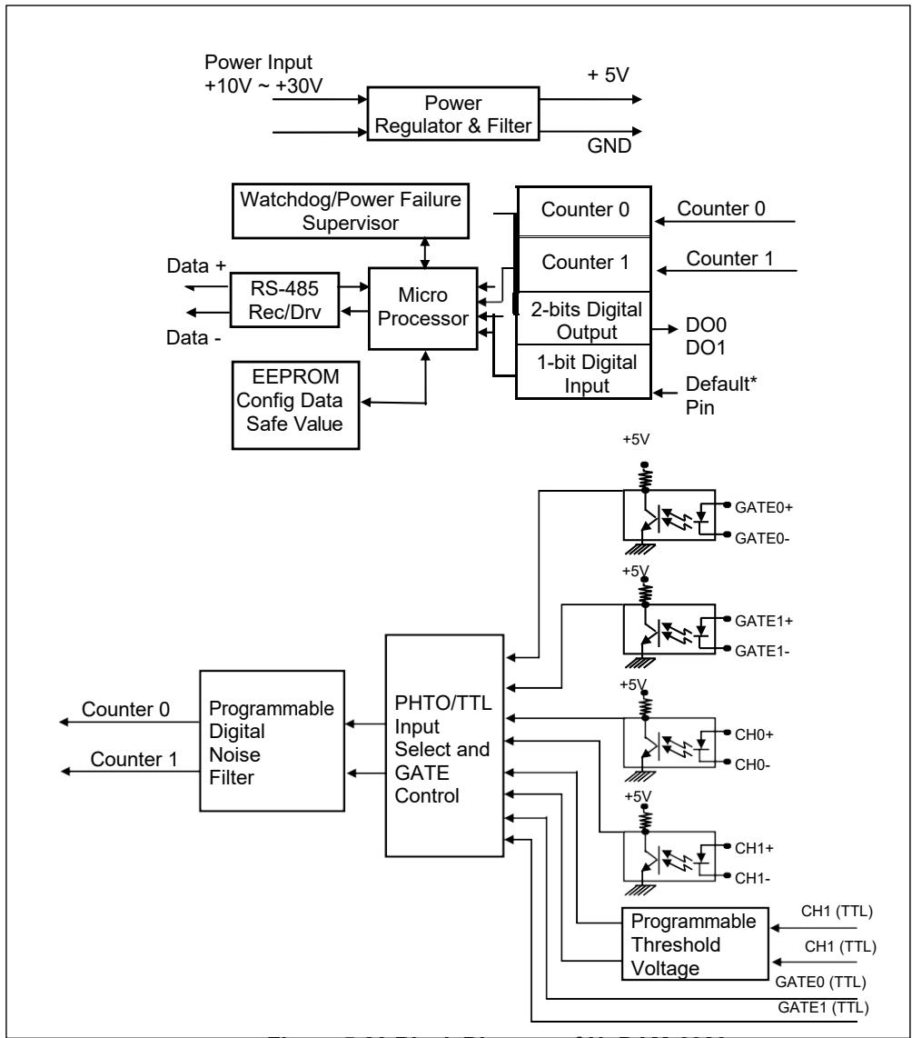
![Based on the provided block diagram, here is the accurate and concise description of the blocks and connections:\n\n**Power and Microcontroller Section**\n*   **Power Input +10V ~ +30V** connects to **Power Regulator & Filter**, which outputs **+ 5V** and **GND**.\n*   **Watchdog/Power Failure Supervisor** connects bidirectionally to **Micro Processor**.\n*   **RS-485 Rec/Drv** connects bidirectionally to **Micro Processor** and has external connections for **Data +** and **Data -**.\n*   **EEPROM Config Data Safe Value** connects bidirectionally to **Micro Processor**.\n\n**Digital I/O Section**\nA vertical block connects to the **Micro Processor** and contains four sub-blocks:\n*   **Counter 0**: Receives external **Counter 0** input.\n*   **Counter 1**: Receives external **Counter 1** input.\n*   **2-bits Digital Output**: Outputs **DO0** and **DO1**.\n*   **1-bit Digital Input**: Receives external **Default* Pin** input.\n\n**Signal Processing and Isolation Section**\n*   **Programmable Digital Noise Filter** connects bidirectionally to **PHTO/TTL Input Select and GATE Control** and outputs **Counter 0** and **Counter 1**.\n*   Four input buffer circuits (depicted with **+5V** pull-up resistors) connect to **PHTO/TTL Input Select and GATE Control**. Their respective inputs are labeled:\n    *   **GATE0+** and **GATE0-**\n    *   **GATE1+** and **GATE1-**\n    *   **CH0+** and **CH0-**\n    *   **CH1+** and **CH1-**\n*   **Programmable Threshold Voltage** receives inputs labeled **CH1 (TTL)**, **CH1 (TTL)**, **GATE0 (TTL)**, and **GATE1 (TTL)** and connects to **PHTO/TTL Input Select and GATE Control**.](.nudam-6000-50m-00083-1000-31/92c25d2d633d0bcc30f96700e4c093aab995f867914d4a2979e0144178d5c061.jpg)

Figure 5-20 Block Diagram of NuDAM-6080

# 6

# Command Set

# 6.1 Command and Response

# 6.1.1 Introduction

The NuDAM command is composed by numbers of characteristics, including the leading code, address ID, the variables and a carriage return to indicate the end of a command. The host computer can only command only one NuDAM module. The slave device may or may not give response to the command.

# Document Conventions

The NuDAM command is composed by numbers of characteristics, including the leading code, address ID, the variables and a carriage return to indicate the end of a command. The host computer can only command only one NuDAM module. The slave device may or may not give response to the command.

<table><tr><td>(Leading Code)</td><td>Leading Code is the first characteristic of the NuDAM command. All NuDAM commands need a command leading code, such as %,$,#,@,...etc.1- character</td></tr><tr><td>(Addr)</td><td>Module&#x27;s address ID, the value is in the range of 00 - FF (Hexadecimal) if no specified in the following.2- character</td></tr><tr><td>(Command Variable)</td><td>Items indicate command codes or value of variables.Variable length</td></tr><tr><td>[Data]</td><td>Some output command need data.Variable length</td></tr><tr><td>[Checksum]</td><td>Checksum in brackets indicate optional parameter, only checksum is enable then this field is required.2- character</td></tr><tr><td>&lt; &gt;</td><td>Identifies a control code character, such asfor carriage return, its value is 0x0D.1- character</td></tr></table>

# 6.1.2 Format of NuDAM Commands

(Leading Code)(Addr)(Command)[Data][Checksum]&lt;CR&gt;

When checksum is enable then [Checksum] is needed, it is 2-character.

How to calculate checksum value ?

[Checksum] = ((LeadingCode)+(Addr)+(Command)+[Data]) MOD 0x100

Example 1: checksum is disable

User Command: \$012&lt;CR&gt; Response: !01400600&lt;CR&gt;

\$ : LeadingCode 01 : Address 2 : Command (Read Configuration) &lt;CR&gt; : Carriage return 0x0D

Example 2: checksum is enable

<table><tr><td colspan="4">User Command: $012B7</td></tr><tr><td colspan="4">Response: !01400600AC</td></tr><tr><td>$</td><td colspan="3">: LeadingCode</td></tr><tr><td>01</td><td colspan="3">: Address</td></tr><tr><td>2</td><td colspan="3">: Command (Read Configuration)</td></tr><tr><td>B7</td><td colspan="3">: Checksum value</td></tr><tr><td>&lt;CR&gt;</td><td colspan="3">: Carriage return 0x0D</td></tr><tr><td>‘$’ = 0x24</td><td>‘0’ = 0x30</td><td>‘1’ = 0x31</td><td>‘2’ = 0x30</td></tr><tr><td colspan="4">B7 = ( 0x24 + 0x30 + 0x31 + 0x32 ) MOD 0x100</td></tr><tr><td>‘!’ = 0x21</td><td>‘0’ = 0x30</td><td>‘1’ = 0x31</td><td>‘4’ = 0x34</td></tr><tr><td colspan="4">‘6’ = 0x36</td></tr><tr><td colspan="4">AC = ( 0x21 + 0x30 + 0x31 + 0x34 + 0x30 + 0x30 + 0x36 + 0x30 + 0x30 ) MOD 0x100</td></tr></table>

Note: 1.There is no spacing between characters.

2. At end of command need a &lt;CR&gt; carriage return 0x0D.

3. Checksum is optional parameter.

# 6.1.3 Response of NuDAM Commands

The response message depends on NuDAM command. The response is also composed with several characteristics, including leading code, variables, and carriage return for ending. There are two kinds of leading code for response message, ”!“ or ”>“ means valid command and ”?“ means invalid. By checking the response message, user can monitor the command is valid or invalid.

Note : Under the following conditions, there will have no response message.

1. The specified address ID is not exist.
2. Syntax error.
3. Communication error
4. Some special commands does not have response.

# 6.2 Summary of Command Set

There are three categories of NuDAM commands. One is the general commands, including set configuration command, read configuration, reset, read module‘s name or firmware version, etc. Every NuDAM can response to the general commands.

The second category is the functional commands, which depends on functions of each module, not every module can execute all functions.

The third category is the special commands, including functions about the programmable watchdog timer, safe values, and the programmable leading code.

<table><tr><td colspan="4">Command Set of Digital I/O Modules</td></tr><tr><td>Command</td><td>Syntax</td><td>Module</td><td>Section</td></tr><tr><td colspan="4">General Commands</td></tr><tr><td>Set Configuration</td><td>%(OldAddr)(NewAddr)(TypeCode)(BaudRate)(CheckSumFlag)</td><td>601x,602x,605x,606x6080,6531</td><td>6.2.1</td></tr><tr><td>Read Configuration</td><td>$(Addr)2</td><td>601x,602x,605x,606x6080,6531</td><td>6.2.2</td></tr><tr><td>Read Module Name</td><td>$(Addr)M</td><td>601x,602x,605x,606x6080,6531</td><td>6.2.3</td></tr><tr><td>Read Firmware Version</td><td>$(Addr)F</td><td>601x,602x,605x,606x6080,6531</td><td>6.2.4</td></tr><tr><td>Reset Status</td><td>$(Addr)5</td><td>601x,602x,605x,606x6080,6531</td><td>6.2.5</td></tr><tr><td>Soft Reset</td><td>$(Addr)RS</td><td>601x,602x,605x,606x6080,6531</td><td>6.2.6</td></tr><tr><td colspan="4">Analog I/O Modules Functional Commands</td></tr><tr><td>Read Analog Data Channel 0</td><td>#(Addr)</td><td>6013</td><td>6.3.1</td></tr><tr><td>Offset Calibration to each Channel</td><td>#(Addr)1(Channel No)</td><td rowspan="2"> $6013^{(11)}$ </td><td>6.3.2</td></tr><tr><td>Span Calibration to ach Channel</td><td>$(Addr)0(Channel No)</td><td>6.3.3</td></tr><tr><td>Read Analog Data From Channel N</td><td>#(Addr)(ChannelNo)</td><td>6013,6017,6018</td><td>6.3.4</td></tr><tr><td>Read All Analog Data Channel</td><td>$(Addr)A</td><td>6013,6017,6018</td><td>6.3.5</td></tr><tr><td>Enable/Disable Channel for Multiplexing</td><td>$(Addr)5(ChannelVal)</td><td>6013,6017, 6018</td><td>6.3.6</td></tr><tr><td>Read Channel Status</td><td>$(Addr)6</td><td>6013,6017, 6018</td><td>6.3.7</td></tr><tr><td>Read CJC Status</td><td>$(Addr)3</td><td>6018</td><td>6.3.8</td></tr><tr><td>Enable/Disable CJC</td><td>$(Addr)C(Status)</td><td> $6018^{(12)}$ </td><td>6.3.9</td></tr><tr><td>Read Enable/Disable CJC Status</td><td>$(Addr)D</td><td> $6018^{(12)}$ </td><td>6.3.10</td></tr><tr><td>CJC Offset Calibration</td><td>$(Addr)9(Counts)</td><td>6018</td><td>6.3.11</td></tr><tr><td>Span Calibration</td><td>$(Addr)0</td><td>6013,6017, 6018</td><td>6.3.12</td></tr><tr><td>Offset Calibration</td><td>$(Addr)1</td><td>6013,6017, 6018</td><td>6.3.13</td></tr><tr><td>Synchronized Sampling</td><td>#**</td><td rowspan="3">6024</td><td>6.4.1</td></tr><tr><td>Read Synchronized Data</td><td>$(Addr)9</td><td>6.4.2</td></tr><tr><td>Digital Input</td><td>$(Addr)8</td><td>6.4.3</td></tr><tr><td rowspan="2">Analog Data Out</td><td># (Addr)(OutData)</td><td>6021</td><td rowspan="2">6.4.4</td></tr><tr><td># (Addr)(Port)(OutData)</td><td>6024</td></tr><tr><td>4 mA Offset Calibration</td><td>$(Addr)0</td><td rowspan="2"> $6021^{(10)}$ </td><td>6.4.5</td></tr><tr><td>20 mA Offset Calibration</td><td>$(Addr)1</td><td>6.4.6</td></tr><tr><td>Trim Calibration</td><td>$(Addr)3(Counts)</td><td>6021,6024</td><td>6.4.7</td></tr><tr><td>Save Power On Analog Value</td><td>$(Addr)4</td><td>6021,6024</td><td>6.4.10</td></tr><tr><td rowspan="2">Last Value Readback</td><td>$(Addr)6</td><td>6021</td><td rowspan="2">6.4.8</td></tr><tr><td>$(Addr)6(Port)</td><td>6024</td></tr><tr><td>Current Readback</td><td>$(Addr)8</td><td>6021</td><td>6.4.9</td></tr><tr><td colspan="4">Digital I/O Modules Functional Commands</td></tr><tr><td>Synchronized Sampling</td><td>#**</td><td>6050, 6052, 6053, 6054, 6058, 6060</td><td>6.5.1</td></tr><tr><td>Read Synchronized Data</td><td>$(Addr)4</td><td>6050, 6052, 6053, 6054, 6058, 6060</td><td>6.5.2</td></tr><tr><td rowspan="4">Digital Output</td><td># (Addr)(ChannelNo) (OutData)</td><td>6050, 6060, 6063</td><td rowspan="4">6.5.3</td></tr><tr><td># (Addr)(Port)(Odata)</td><td rowspan="2">6056, 6058</td></tr><tr><td># (Addr)(Port)(ChannelNo)(BitData)</td></tr><tr><td># (Addr)T(OdataA)(OdataB)(OdataC)</td><td>6058</td></tr><tr><td>Digital Input</td><td>$(Addr)6</td><td>605x,606x</td><td>6.5.4</td></tr><tr><td>Set Programmable I/O Mode</td><td>$(Addr)S(IOSts)</td><td>6058</td><td>6.5.5</td></tr><tr><td colspan="4">Communication Module Functional Commands</td></tr><tr><td>Set RTS Status</td><td>$(Addr)0(RTS Status)</td><td>6531</td><td>6.6.1</td></tr><tr><td>Read RTS Status</td><td>$(Addr)3</td><td>6531</td><td>6.6.2</td></tr><tr><td>Read CTS Status</td><td>$(Addr)1</td><td>6531</td><td>6.6.3</td></tr><tr><td>Set Device ID</td><td>$(Addr)6(Device ID)</td><td>6531</td><td>6.6.4</td></tr><tr><td>Read Device ID</td><td>$(Addr)7</td><td>6531</td><td>6.6.5</td></tr><tr><td>Set Delimiter</td><td>$(Addr)C(Delimiter)</td><td>6531</td><td>6.6.6</td></tr><tr><td>Read Delimiter</td><td>$(Addr)D</td><td>6531</td><td>6.6.7</td></tr><tr><td>Data Pass</td><td>(Delimiter)(Addr)(Data)</td><td>6531</td><td>6.6.8</td></tr><tr><td>Open/Close Data Gate</td><td>&amp;(Addr)8(Data Gate Mode)</td><td>6531</td><td>6.6.9</td></tr><tr><td colspan="4">Counter/Frequency Input Module Functional Commands</td></tr><tr><td>Set Input Signal Mode</td><td>$(Addr)B(InType)</td><td>6080</td><td>6.7.1</td></tr><tr><td>Read Input Signal Mode</td><td>$(Addr)B</td><td>6080</td><td>6.7.2</td></tr><tr><td>Read Counter/Frequency Value in Hexadecimal</td><td>#(Addr)(CounterNo)</td><td>6080</td><td>6.7.3</td></tr><tr><td>Read Counter/Frequency Value in Decimal</td><td>#(Addr)(CounterNo)D</td><td>6080</td><td>6.7.4</td></tr><tr><td>Set Gate Mode</td><td>$(Addr)A(Gmode)</td><td>6080</td><td>6.7.5</td></tr><tr><td>Read Gate Mode</td><td>$(Addr)A</td><td>6080</td><td>6.7.6</td></tr><tr><td>Set Maximum Counter Value</td><td>$(Addr)3(CounterNo)(MaxData)</td><td>6080</td><td>6.7.7</td></tr><tr><td>Read Maximum Counter Value</td><td>$(Addr)3(CounetrNo)</td><td>6080</td><td>6.7.8</td></tr><tr><td>Set Initial Count Value</td><td>@(Addr)P(CounterNo)(IniData)</td><td>6080</td><td>6.7.9</td></tr><tr><td>Read Initial Count Value</td><td>@(Addr)G(CounetrNo)</td><td>6080</td><td>6.7.10</td></tr><tr><td>Start/Stop Counter</td><td>$(Addr)5(CounterNo)(SStatus)</td><td>6080</td><td>6.7.11</td></tr><tr><td>Read Counter Start/Stop Status</td><td>$(Addr)5(CounterNo)</td><td>6080</td><td>6.7.12</td></tr><tr><td>Clear Counter</td><td>$(Addr)6(CounterNo)</td><td>6080</td><td>6.7.13</td></tr><tr><td>Read then Clear the Overflow Flag</td><td>$(Addr)7(CounterNo)</td><td>6080</td><td>6.7.14</td></tr><tr><td>Enable/Disable Digital Filter</td><td>$(Addr)4(FStatus)</td><td>6080</td><td>6.7.15</td></tr><tr><td>Read Filter Status</td><td>$(Addr)4</td><td>6080</td><td>6.7.16</td></tr><tr><td>Set Minimum Input Signal Width at High Level</td><td>$(Addr)0H(MinFData)</td><td>6080</td><td>6.7.17</td></tr><tr><td>Read Minimum Input Signal Width at High Level</td><td>$(Addr)0H</td><td>6080</td><td>6.7.18</td></tr><tr><td>Set Minimum Input Signal Width at Low Level</td><td>$(Addr)0L(MinFData)</td><td>6080</td><td>6.7.19</td></tr><tr><td>Read Minimum Input Signal Width at Low Level</td><td>$(Addr)0L</td><td>6080</td><td>6.7.20</td></tr><tr><td>Set TTL Input High Trigger Level</td><td>$(Addr)1H(ThData)</td><td>6080</td><td>6.7.21</td></tr><tr><td>Read TTL Input High Trigger Level</td><td>$(Addr)1H</td><td>6080</td><td>6.7.22</td></tr><tr><td>Set TTL Input Low Trigger Level</td><td>$(Addr)1L(ThData)</td><td>6080</td><td>6.7.23</td></tr><tr><td>Read TTL Input Low Trigger Level</td><td>$(Addr)1L</td><td>6080</td><td>6.7.24</td></tr><tr><td>Enable Alarm</td><td>@(Addr)EA(CounterNo)</td><td>6080</td><td>6.7.25</td></tr><tr><td>Disable Alarm</td><td>@(Addr)DA(CounterNo)</td><td>6080</td><td>6.7.26</td></tr><tr><td>Set Alarm Limit Value of Counter 0</td><td>@(Addr)PA(ArmData)</td><td>6080</td><td>6.7.27</td></tr><tr><td>Set Alarm Limit Value of Counter 1</td><td>@(Addr)SA(ArmData)</td><td>6080</td><td>6.7.28</td></tr><tr><td>Read Alarm Limit Value of Counter 0</td><td>@(Addr)RP</td><td>6080</td><td>6.7.29</td></tr><tr><td>Read Alarm Limit Value of Counter 1</td><td>@(Addr)RA</td><td>6080</td><td>6.7.30</td></tr><tr><td>Set Digital Output Values</td><td>@(Addr)DO(DoData)</td><td>6080</td><td>6.7.31</td></tr><tr><td>Read Digital Output and Alarm Status</td><td>@(Addr)DI</td><td>6080</td><td>6.7.32</td></tr><tr><td colspan="4">Special Commands</td></tr><tr><td>Read Command Leading Code Setting</td><td>~(Addr)0</td><td>601x,602x,605x,606x,6080,6531</td><td>6.8.1</td></tr><tr><td>Change Command Leading Code Setting</td><td>~(Addr)10(C1)(C2)(C3)(C4)(C5)(C6)</td><td>601x,602x,605x,606x,6080,6531</td><td>6.8.2</td></tr><tr><td rowspan="2">Set Host Watchdog / Safety Value</td><td>~(Addr)2(Flag)(TimeOut)(SafeValue)</td><td>6021,605x,606x,6531</td><td rowspan="2">6.8.3</td></tr><tr><td>~(Addr)2(Flag)(TimeOut)(SafeA)(SafeB)(SafeC)(SafeD)</td><td>6024</td></tr><tr><td>Read Host WatchDog / Safe Value</td><td>~(Addr)3</td><td>602x,605x,606x6080,6531</td><td>6.8.4</td></tr><tr><td>Change Polarity</td><td>~(Addr)CP(Status)</td><td>605X,606X</td><td>6.8.5</td></tr><tr><td>Read Polarity</td><td>~(Addr)CR</td><td>605X,606X</td><td>6.8.6</td></tr><tr><td>Host is OK</td><td>~**</td><td>601x,602x,605x,606x6080,6531</td><td>6.8.7</td></tr></table>

Note : “601x” means forND-6013, ND-6017 and ND-6018. “602x” means for ND-6021 and ND-6024. “605x” means forND-6050, ND-6052, ND-6053, ND-6054, ND-6056, and ND-6058. “606x” means for ND-6063 and ND-6067.

Note(10) : This function only support on F/W version above A4.30.

Note(11) : These two functions only support between F/W versionA3.05 to A4.52.

Note(12) : These two functions support on F/W version above B1.31of ND-6018 and F/W version above C4.60 of ND-6013.

# 6.2.1 Set Configuration

(601x,602x,605x,606x,

6080,6531)

# @Description

Configure the basic setting of NuDAM, including the address ID, input range, baud rate, and data format. The new configuration will be available after executing the command.

# @Syntax

%(OldAddr)(NewAddr)(InputRange/OutputRange/TypeCod e)(BaudRate)(DataFormat/CheckSumFlag/DataFlag)&lt;CR&gt;

<table><tr><td>%</td><td colspan="2">Command leading code. (1-character)</td></tr><tr><td>(OldAddr)</td><td colspan="2">NuDAM module original address ID. The default address ID of a brand new module is 01. The value range of address ID is 00 to FF in hexadecimal.(2-character)</td></tr><tr><td>(NewAddr)</td><td colspan="2">New address ID, if you don’t want to change address ID, let new address ID equals to the old one. (2-character)</td></tr><tr><td>(InputRange)</td><td>Define analog input range, refers to Table 6-1 for details. (2-character)</td><td>601x</td></tr><tr><td>(OutputRange)</td><td>Define analog output range, refers to Table 6-2 for details. (2-character)</td><td>602x</td></tr><tr><td rowspan="2">(TypeCode)</td><td>Type Code is fixed 40H for Digital I/O modules. (2-character)</td><td>605x,606x, 6531</td></tr><tr><td>Type Code represents the input mode. (2-character)50: counter input mode51: frequency input mode</td><td>6080</td></tr><tr><td>(BaudRate)</td><td colspan="2">Define communication baud rate, refers to Table 6-3 for details. (2-character)</td></tr><tr><td>(DataFormat)</td><td>Define checksum, integration time and output data format, refers to Figure 6-1 for details. (2-character)</td><td>601x</td></tr><tr><td rowspan="2">(CheckSumFlag)</td><td>Define checksum, integration time and output data format, refers to Figure 6-2 for details. (2-character)</td><td>602x</td></tr><tr><td>Define check-sum status, refer to Figure 6-3 for details. (2-character)</td><td>605x</td></tr><tr><td rowspan="2">(DataFlag)</td><td>Define check-sum status, refer to Figure 6-4 for details. (2-character)</td><td>6080</td></tr><tr><td>Define check-sum status, refer to Table 6-4 for details. (4-character,WXYZ) WX is for module system setting. YZ is for RS-232 configuration.</td><td>6531</td></tr></table>

# @Response

!(Addr)&lt;CR&gt;

or

?(Addr)&lt;CR&gt;

(Addr)

Address ID.

!

Command is valid.

Command is invalid, parameter values are invalid, or change the setting without grounding the DEFAULT\* pin.

Note: When you want to change the checksum or baud rate, the DEFAULT\* pin must be grounded at first.

# @Example 1 &lt;ND-601x&gt;

User command: %0130050600&lt;CR&gt;

Response: !30&lt;CR&gt;

<table><tr><td>Item</td><td>Meaning</td><td>Description</td></tr><tr><td>%</td><td>(Leading Code)</td><td>Command leading code.</td></tr><tr><td>01</td><td>(OldAddr)</td><td>Original address ID is 01(Hex).</td></tr><tr><td>30</td><td>(NewAddr)</td><td>New address ID is 30(Hex).</td></tr><tr><td>05</td><td>(InputRange)</td><td>Analog input range is ±2.5V</td></tr><tr><td>06</td><td>(BaudRate)</td><td>Baud rate is 9600.</td></tr><tr><td>00</td><td>(DataFormat)</td><td>00 means data format is engineering units, checksum is disable and integration time is 50 ms (60Hz).</td></tr><tr><td></td><td>Carriage return</td><td>0x0D.</td></tr></table>

<table><tr><td>Code (Hex)</td><td>Input Range</td><td>Modules</td></tr><tr><td>00</td><td>±15 mV</td><td>6018</td></tr><tr><td>01</td><td>±50 mV</td><td>6018</td></tr><tr><td>02</td><td>±100 mV</td><td>6018</td></tr><tr><td>03</td><td>±500 mV</td><td>6018</td></tr><tr><td>04</td><td>±1 V</td><td>6018</td></tr><tr><td>05</td><td>±2.5 V</td><td>6018</td></tr><tr><td>06</td><td>±20 mA(Required 125^ current conversion resistor.)</td><td>6018</td></tr><tr><td>08</td><td>±10 V</td><td>6017</td></tr><tr><td>09</td><td>±5 V</td><td>6017</td></tr><tr><td>0A</td><td>±1 V</td><td>6017</td></tr><tr><td>0B</td><td>±500 mV</td><td>6017</td></tr><tr><td>0C</td><td>±150 mV</td><td>6017</td></tr><tr><td>0D</td><td>±20 mA(Required 125^ current conversion resistor.)</td><td>6017</td></tr><tr><td>0E</td><td>Type J Thermocouple 0° to 760°C</td><td>6018</td></tr><tr><td>0F</td><td>Type K Thermocouple 0° to 1370°C</td><td>6018</td></tr><tr><td>10</td><td>Type T Thermocouple -100° to 400°C</td><td>6018</td></tr><tr><td>11</td><td>Type E Thermocouple 0° to 1000°C</td><td>6018</td></tr><tr><td>12</td><td>Type R Thermocouple 500° to 1750°C</td><td>6018</td></tr><tr><td>13</td><td>Type S Thermocouple 500° to 1750°C</td><td>6018</td></tr><tr><td>14</td><td>Type B Thermocouple 500° to 1800°C</td><td>6018</td></tr><tr><td>15</td><td>Type N Thermocouple -270° to 1300°C</td><td>6018</td></tr><tr><td>16</td><td>Type C Thermocouple 0° to 2320°C</td><td>6018</td></tr><tr><td>20</td><td>Pt-100, -100°C to +100°C, α=0.00385</td><td>6013</td></tr><tr><td>21</td><td>Pt-100, 0°C to +100°C, α=0.00385</td><td>6013</td></tr><tr><td>22</td><td>Pt-100, 0°C to +200°C, α=0.00385</td><td>6013</td></tr><tr><td>23</td><td>Pt-100, 0°C to +600°C, α=0.00385</td><td>6013</td></tr><tr><td>24</td><td>Pt-100, -100°C to +100°C, α=0.003916</td><td>6013</td></tr><tr><td>25</td><td>Pt-100, 0°C to +100°C, α=0.003916</td><td>6013</td></tr><tr><td>26</td><td>Pt-100, 0°C to +200°C, α=0.003916</td><td>6013</td></tr><tr><td>27</td><td>Pt-100, 0°C to +600°C, α=0.003916</td><td>6013</td></tr><tr><td>28</td><td>Ni-100, 0°C to +100°C</td><td>6013</td></tr><tr><td>29</td><td>Ni-120, 0°C to +100°C</td><td>6013</td></tr><tr><td>2A</td><td>0~60 Ohms</td><td>6013</td></tr></table>

Table 6-1 AD Input Range Setting

@Example 2 &lt;ND-602x&gt;

<table><tr><td>User command:</td><td>%0118310610</td></tr><tr><td>Response:</td><td>!18</td></tr></table>

<table><tr><td>Item</td><td>Meaning</td><td>Description</td></tr><tr><td>%</td><td>(Leading Code)</td><td>Command leading code.</td></tr><tr><td>01</td><td>(OldAddr)</td><td>Original address ID is 01(Hex).</td></tr><tr><td>18</td><td>(NewAddr)</td><td>New address ID is 18(Hex).</td></tr><tr><td>31</td><td>(OutputRange)</td><td>Analog output range is 4 to 20 mA</td></tr><tr><td>06</td><td>(BaudRate)</td><td>Baud rate is 9600.</td></tr><tr><td>10</td><td>(DataFormat)</td><td>10 means a slew rate is 1.000 mA/sec and checksum is disable.</td></tr><tr><td></td><td>Carriage return</td><td>0x0D.</td></tr></table>

<table><tr><td>Code (Hex)</td><td>Signal Range of Output Range</td><td>Modules</td></tr><tr><td>30</td><td>0 to 20 mA</td><td>6021</td></tr><tr><td>31</td><td>4 to 20 mA</td><td>6021</td></tr><tr><td>32</td><td>0 to 10 V</td><td>6021</td></tr><tr><td>33</td><td>-10 to 10 V</td><td>6024</td></tr></table>

Table 6-2 Analog Output Range Setting

@Example 3 &lt;ND-605x&gt;

<table><tr><td>User command:</td><td>%0130400600</td></tr><tr><td>Response:</td><td>!30</td></tr></table>

<table><tr><td>Item</td><td>Meaning</td><td>Description</td></tr><tr><td>%</td><td>(Leading Code)</td><td>Command leading code.</td></tr><tr><td>01</td><td>(OldAddr)</td><td>Original address ID is 01H.</td></tr><tr><td>30</td><td>(NewAddr)</td><td>New address ID is 30H (Hex).</td></tr><tr><td>40</td><td>(TypeCode)</td><td>Digital I/O module.</td></tr><tr><td>06</td><td>(BaudRate)</td><td>Baud rate is 9600.</td></tr><tr><td>00</td><td>(CheckSumFlag)</td><td>00 means checksum is disable.</td></tr><tr><td></td><td>Carriage return</td><td>0x0D.</td></tr></table>

@Example 4 &lt;ND-6531&gt;

<table><tr><td>User ommand:</td><td>%013040662103</td></tr><tr><td>Response:</td><td>!30</td></tr></table>

<table><tr><td>Item</td><td>Meaning</td><td>Description</td></tr><tr><td>%</td><td>(Leading Code)</td><td>Command leading code.</td></tr><tr><td>01</td><td>(OldAddr)</td><td>Original address ID is 01H.</td></tr><tr><td>30</td><td>(NewAddr)</td><td>New address ID is 30H (Hex).</td></tr><tr><td>40</td><td>(TypeCode)</td><td>6531 module.</td></tr><tr><td>6</td><td>(BaudRate for RS-422/485)</td><td>Baud rate is 9600 for RS-422/485.</td></tr><tr><td>6</td><td>(BaudRate for RS-232)</td><td>Baud rate is 9600 for RS-232.</td></tr><tr><td>2103</td><td>(DataFlag)</td><td>Addressable modeChecksum is disableRS-485 interfaceAppend&lt;CR&gt;Non-parity8 data bit</td></tr><tr><td></td><td>Carriage return</td><td>0x0D.</td></tr></table>

<table><tr><td>Code</td><td>Baudrate</td></tr><tr><td>3</td><td>1200 bps</td></tr><tr><td>4</td><td>2400 bps</td></tr><tr><td>5</td><td>4800 bps</td></tr><tr><td>6</td><td>9600 bps</td></tr><tr><td>7</td><td>19200 bps</td></tr><tr><td>8</td><td>38400 bps</td></tr><tr><td>9</td><td>115200 bps</td></tr><tr><td>A</td><td>57600 bps</td></tr></table>

Table 6-3. Baud rate setting code

![Flowchart](.nudam-6000-50m-00083-1000-31/a611b7d8c6565af12f1d03a75bf5741c795a632608e2ab55dce39e348d3bee45.jpg)

Figure 6-1 Data Format Setting of ND-601x

![| Bit Code Voltage Current | immediate change(13) |\n| ------------------------ | --------------------- |\n| 0001                     | 0.0625 V/sec         |\n| 0010                     | 0.125 V/sec           |\n| 0011                     | 0.250 V/sec           |\n| 0100                     | 0.500 V/sec           |\n| 0101                     | 1.000 V/sec           |\n| 0110                     | 2.000 V/sec           |\n| 0111                     | 4.000 V/sec           |\n| 1000                     | 8.000 V/sec           |\n| 1001                     | 16.00 V/sec           |\n| 1010                     | 32.00 V/sec           |\n| 1011                     | 64.00 V/sec           |](.nudam-6000-50m-00083-1000-31/ddf3a6e6c4c43eb58eaaef95dfb1b10e6753377ab5983f07682bfa0de737796f.jpg)

![The image displays a simple black line drawing on a white background, framed by thick black vertical bars along the far left and right edges. A thin black line extends horizontally from the right side towards the left, then turns diagonally downward to the left, terminating in an arrowhead pointing towards the bottom left. There is no text present in the image.](.nudam-6000-50m-00083-1000-31/75f1d272ade3c9e08323f0ab4f2104a002f1289afa4aa917219e4e830ff36058.jpg)

0 : disable

1 : enable

![7 6 5 4 3 2 1 0\nAn](.nudam-6000-50m-00083-1000-31/86f8db5bdd8d3ab3fec0878c9921decf78c2c490cee85dc329ea4128b3ea912b.jpg)

<table><tr><td>0001</td><td>0.0625</td><td>V/sec</td><td>0.125 mA/sec</td></tr><tr><td>0010</td><td>0.125</td><td>V/sec</td><td>0.250 mA/sec</td></tr><tr><td>0011</td><td>0.250</td><td>V/sec</td><td>0.500 mA/sec</td></tr><tr><td>0100</td><td>0.500</td><td>V/sec</td><td>1.000 mA/sec</td></tr><tr><td>0101</td><td>1.000</td><td>V/sec</td><td>2.000 mA/sec</td></tr><tr><td>0110</td><td>2.000</td><td>V/sec</td><td>4.000 mA/sec</td></tr><tr><td>0111</td><td>4.000</td><td>V/sec</td><td>8.000 mA/sec</td></tr><tr><td>1000</td><td>8.000</td><td>V/sec</td><td>16.00 mA/sec</td></tr><tr><td>1001</td><td>16.00</td><td>V/sec</td><td>32.00 mA/sec</td></tr><tr><td>1010</td><td>32.00</td><td>V/sec</td><td>64.00 mA/sec</td></tr><tr><td>1011</td><td>64.00</td><td>V/sec</td><td>128.0 mA/sec</td></tr></table>

00 : Engineering units

01 : % of Full Scale Range

10 : Hexadecimal

Figure 6-2 Data format of ND-602x

Note(13) : 6024 only supports immediate change and engineering units.

![Checksum\n0 : disable\n1 : enable\nReserved\nMust to be 0\nReserved\nMust to be 000000](.nudam-6000-50m-00083-1000-31/c014318e555b9dd3504ca0c7183ba82e64782f1c7575a9f7f5e01c01212ad261.jpg)

Figure 6-3 Check sum flag setting of 605x

![This diagram illustrates a data register structure, likely 8 bytes or 32 bits wide, represented by a main horizontal row of 8 blocks. Below this main row, there is a secondary section of blocks aligned underneath the middle and right portions (roughly under the 4th through 7th blocks).\n\nThe labeled blocks and their connections are:\n\n*   **Checksum** (Top Left Box): Contains the text '0 : disable' and '1 : enable'. An arrow points from this box to the **leftmost block** of the top row.\n*   **Frequency Gate Time** (Top Right Box): Contains the text '0 : 0.1 second' and '1 : 1 second'. An arrow points from this box to the **sixth block** (second from the right) of the top row.\n*   **Reserved** (Bottom Left Box): Contains the text 'Must to be 0'. An arrow points from this box to the **leftmost block** of the top row.\n*   **Reserved** (Bottom Right Box): Contains the text 'Must to be 000000'. An arrow points from this box to the **lower-right section** of the diagram, specifically the wide block situated beneath the sixth and seventh blocks of the top row.](.nudam-6000-50m-00083-1000-31/c905520b98ba9aee368e1d3a9a80c437e2073139bc1e94aaa7fe59dd538f9cfe.jpg)

Figure 6-4 Check sum flag setting of 6080

<table><tr><td rowspan="2">W. bit 3</td><td>0</td><td>Normal addressable mode (*Default Setting)</td></tr><tr><td>1</td><td>Non-addressable mode (ND-6520 mode)</td></tr><tr><td rowspan="2">W. bit 2</td><td>0</td><td>Disable checksum (*Default Setting)</td></tr><tr><td>1</td><td>Enable checksum</td></tr><tr><td rowspan="2">W. bit 1</td><td>0</td><td>RS-422 interface</td></tr><tr><td>1</td><td>RS-485 interface (*Default Setting)</td></tr><tr><td>W. bit 0</td><td>0</td><td rowspan="4">Don&#x27;t care, set to 0</td></tr><tr><td>X. bit 3</td><td>0</td></tr><tr><td>X. bit 2</td><td>0</td></tr><tr><td>X. bit 1</td><td>0</td></tr><tr><td rowspan="2">X. bit 0</td><td>0</td><td>Don&#x27;t appendin output string</td></tr><tr><td>1</td><td>Appendin output string(*Default Setting)</td></tr><tr><td>Y. bit 3</td><td>0</td><td rowspan="3">Don&#x27;t care, set to 0</td></tr><tr><td>Y. bit 2</td><td>0</td></tr><tr><td>Y. bit 1</td><td>0</td></tr><tr><td rowspan="2">Y. bit 0</td><td>0</td><td>Odd parity (*Default Setting)</td></tr><tr><td>1</td><td>Even parity</td></tr><tr><td rowspan="2">Z. bit 3</td><td>0</td><td>Non-parity mode (*DefaultSetting)</td></tr><tr><td>1</td><td>Parity mode</td></tr><tr><td rowspan="2">Z. bit 2</td><td>0</td><td>One stop bit (*Default Setting)</td></tr><tr><td>1</td><td>Two stop bit</td></tr><tr><td rowspan="4">Z. bit 1 0</td><td>00</td><td>5 data bit format</td></tr><tr><td>01</td><td>6 data bit format</td></tr><tr><td>10</td><td>7 data bit format</td></tr><tr><td>11</td><td>8 data bit format</td></tr></table>

Table 6-4. Data Flag code of 6531

# 6.2.2 Read Configuration

(601x,602x,605x,606x,

6080,6531)

# @Description

Read the configuration of module on a specified address ID.

# @Syntax

\$(Addr)2&lt;CR&gt;

<table><tr><td>$</td><td>Command leading code</td></tr><tr><td>(Addr)</td><td>Address ID.</td></tr><tr><td>2</td><td>Command code for reading configuration</td></tr></table>

# @Response

!(Addr)(InputRange/OutputRange/TypeCode)(BaudRate)( DataFormat/CheckSumFalg/DataFlag)&lt;CR&gt;
or ?(Addr)&lt;CR&gt;

<table><tr><td>!</td><td colspan="2">Command is invalid.</td></tr><tr><td>?</td><td colspan="2">Command is invalid.</td></tr><tr><td>(Addr)</td><td colspan="2">Address ID.</td></tr><tr><td>(InputRange)</td><td>Current setting of analog voltage input, refers to Table 6-1 for details.</td><td>601x</td></tr><tr><td>(OutputRange)</td><td>Current setting of analog voltage output, refers to Table 6-2 for details.</td><td>602x</td></tr><tr><td rowspan="2">(TypeCode)</td><td>It always be 40 (Hex) for digital I/O modules.</td><td>605x, 606x, 6531</td></tr><tr><td>Type Code represents the input mode. (2-character)50: counter input mode51: frequency input mode</td><td>6080</td></tr><tr><td>(BaudRate)</td><td colspan="2">Define communication baud rate, refers to Table 6-3 for details. (2-character)</td></tr><tr><td rowspan="2">(DataFormat)</td><td>Current settings of checksum, integration time and output data format, refers to Figure 6-1 for details.</td><td>601x</td></tr><tr><td>Current settings of checksum, integration time and output data format, refers to Figure 6-2 for details.</td><td>602x</td></tr><tr><td rowspan="2">(CheckSumFlag)</td><td>Current setting of check-sum flag, refer to Figure 6-5 for details. (2-character)</td><td>605x</td></tr><tr><td>Current setting of check-sum flag, refer to Figure 6-4 for details. (2-character)</td><td>6080</td></tr><tr><td>(DataFlag)</td><td>Current setting of module setting and RS-232 configuration refer to Table 6-4 for details. (4-character,WXYZ)</td><td>6531</td></tr></table>

@Example 1 &lt;ND-601x&gt;

<table><tr><td>User command:</td><td>$302</td></tr><tr><td>Response:</td><td>!30050600</td></tr><tr><td>!</td><td>Command is valid.</td></tr><tr><td>30</td><td>Address ID.</td></tr><tr><td>05</td><td>Analog input range is  $\pm 2.5$  V.</td></tr><tr><td>06</td><td>Baud rate is 9600 bps.</td></tr><tr><td>00</td><td>checksum is disable.</td></tr></table>

@Example 2 &lt;ND-602x&gt;

<table><tr><td>User command:</td><td>$182</td></tr><tr><td>Response:</td><td>!18320610</td></tr></table>

<table><tr><td>!</td><td>Command is valid.</td></tr><tr><td>18</td><td>Address ID.</td></tr><tr><td>32</td><td>Analog output range is 0 to 10V</td></tr><tr><td>06</td><td>Baud rate is 9600 bps.</td></tr><tr><td>10</td><td>The output data is in engineering units, slew rate is 1mA/sec, checksum is disable.</td></tr></table>

@Example 3 &lt;ND-605x&gt;

<table><tr><td>User command:</td><td>$302</td></tr><tr><td>Response:</td><td>!30400600</td></tr></table>

<table><tr><td>!</td><td>Command is valid.</td></tr><tr><td>30</td><td>Address ID.</td></tr><tr><td>40</td><td>Digital I/O module.</td></tr><tr><td>06</td><td>Baud rate is 9600 bps.</td></tr><tr><td>00</td><td>checksum is disable.</td></tr></table>

Checksum

0 : disable

1 : enable

![Reserved\nReserved Must to be\n000](.nudam-6000-50m-00083-1000-31/b431023166e3ce30fc828bdeb336983655e4bb99dcfcb55dcb4c11ce798bb05b.jpg)

Must to be 0

Module Type

000: ND-6050

001: ND-6060

011: ND-6053

100: ND-6058

101: ND-6063

110: ND-6054

111: ND-6056

Figure 6-5 Response of check sum flag
@Example 4 &lt;ND-6080&gt;

<table><tr><td>User command:</td><td>$302</td></tr><tr><td>Response:</td><td>!30500600</td></tr></table>

<table><tr><td>!</td><td>Command is valid.</td></tr><tr><td>30</td><td>Address ID.</td></tr><tr><td>50</td><td>Counter Input Mode.</td></tr><tr><td>06</td><td>Baud rate is 9600 bps.</td></tr><tr><td>00</td><td>checksum is disable, frequency gate is 0.1 second.</td></tr></table>

@Example 5 &lt;ND-6531&gt;

<table><tr><td>User command:</td><td>$302</td></tr><tr><td>Response:</td><td>!3040662103</td></tr></table>

<table><tr><td>!</td><td>Command is valid.</td></tr><tr><td>30</td><td>Address ID.</td></tr><tr><td>40</td><td>Digital I/O module.</td></tr><tr><td>66</td><td>Baud rate is 9600 for RS-422/485 and RS-232.</td></tr><tr><td>2103</td><td>Addressable mode</td></tr><tr><td></td><td>Checksum is disable</td></tr><tr><td></td><td>RS-485 interface</td></tr><tr><td></td><td>Append</td></tr><tr><td></td><td>Non-parity</td></tr><tr><td></td><td>8 data bit</td></tr></table>

# 6.2.3 Read Module Name

(601x,602x,605x,60

6x,6080,6531)

# @Description

Read NuDAM module‘s name.

# @Syntax

\$(Addr)M&lt;CR&gt;

<table><tr><td>$</td><td>Command leading code.</td></tr><tr><td>(Addr)</td><td>Address ID.</td></tr><tr><td>M</td><td>Read module name.</td></tr></table>

# @Response

!(Addr)(ModuleName) &lt;CR&gt;

or

?(Addr)&lt;CR&gt;

<table><tr><td>!</td><td>Command is valid.</td></tr><tr><td>?</td><td>Command is invalid.</td></tr><tr><td>(Addr)</td><td>Address ID.</td></tr><tr><td>(ModuleName)</td><td>NuDAM module‘s name.</td></tr></table>

# @Example

<table><tr><td>User command:</td><td>$30M</td></tr><tr><td>Response:</td><td>!306050</td></tr></table>

<table><tr><td>!</td><td>Command is valid</td></tr><tr><td>30</td><td>Address.</td></tr><tr><td>6050</td><td>ND-6050 (Digital I/O module).</td></tr></table>

# 6.2.4 Read Firmware Version

(601x,602x,605x,60

6x,6080,6531)

# @Description

Read firmware version of NuDAM at specified address.

# @Syntax

\$(Addr)F&lt;CR&gt;

\$ Command leading code.

(Addr) Address ID

F Read module firmware version.

# @Response

!(Addr)(FirmRev) &lt;CR&gt;

or

?(Addr)&lt;CR&gt;

<table><tr><td>!</td><td>Command is valid.</td></tr><tr><td>?</td><td>Command is invalid.</td></tr><tr><td>(Addr)</td><td>Address ID.</td></tr><tr><td>(FirmRev)</td><td>NuDAM module&#x27;s firmware version.</td></tr></table>

# @Example

<table><tr><td>User command:</td><td>$18F</td></tr><tr><td>Response:</td><td>!18A2.30</td></tr></table>

<table><tr><td>!</td><td>Command is valid.</td></tr><tr><td>18</td><td>Address ID is 18 (Hex).</td></tr><tr><td>A2.30</td><td>Firmware Version</td></tr></table>

# 6.2.5 Reset Status

(601x,602x,605x,60

6x,6080,6531)

# @Description

Read the reset status of module at specified address to check whether if it has been reset since the last reset status command was issued to the module.

# @Syntax

\$(Addr)5&lt;CR&gt;

\$

Command leading code.

Address ID.

5

Reset Status Command.

# @Response

!(Addr)(Status)&lt;CR&gt;

?(Addr)&lt;CR&gt;

!

Command is valid.

?

Command is invalid.

Address ID.

0 : It has not been reset since the last reset status command was issued.

1 : It has been reset since the last reset status command was issued.

# @Example

User command: \$185&lt;CR&gt;

Response: !180&lt;CR&gt;

Status is 0 means this digital I/O module has not been reset, since the last reset status command was issued.

# 6.2.6 Soft Reset

(601x,602x,605x,60

6x,6080,6531)

# @Description

Reset the module by software command

# @Syntax

\$(Addr)RS&lt;CR&gt;

Command leading code.

(Addr)

Address ID

RS

Soft Reset Command

# @Response

!(Addr)&lt;CR&gt;

or

?(Addr)&lt;CR&gt;

!

Command is valid.

?

Command is invalid.

(Addr)

Address ID.

# @Example

User command: \$30RS&lt;CR&gt;

Response:

!30&lt;CR&gt;

# 6.3.1 Read Analog Data

# @Description

Read the analog input value from an analog input module at specified address in a NuDAM network. While for ND-6013, it returns the channel 0 analog data.

# @Syntax

# #(Addr)&lt;CR&gt;

\#

(Addr)

Command leading code

Address ID

# @Response

# >(InputData)&lt;CR&gt;

>

(InputData)

Delimiter character

The input data represents the analog signal. The unit of the digits depends on the data format used. There are four types of data format. The format is set by the set configuration command. Delimiter character

# @Example

```txt
User command: #06&lt;CR&gt;
Response: >+1.6888&lt;CR&gt;
```

Read the analog input module data at address 06 (Hex). The analog input module response data is +1.6888 units. The unit depends on the data format.

# 6.3.2 Offset Calibration to each Channel

(6013(14))

# @Description

To correct the offset errors of AD converter by using the offset calibration.

# @Syntax

\$(Addr)1(Channel No)&lt;CR&gt;

<table><tr><td>$</td><td>Command leading code</td></tr><tr><td>(Addr)</td><td>Address ID</td></tr><tr><td>1</td><td>Offset calibration.</td></tr><tr><td>(Channel No)</td><td>Channel for calibration.(1 character)0~2</td></tr></table>

# @Response

!(Addr)&lt;CR&gt;

<table><tr><td colspan="2">or</td></tr><tr><td>?(Addr)</td><td></td></tr><tr><td>!</td><td>Command is valid.</td></tr><tr><td>?</td><td>Command is invalid.</td></tr><tr><td>(Addr)</td><td>Address ID.</td></tr></table>

# @Example

<table><tr><td>User command:</td><td>$0612</td></tr><tr><td>Response:</td><td>!06</td></tr></table>

To perform the offset calibration for analog input module ND-6013 channel 2 at specified address 06 (Hex).

Note: To perform the calibration, a proper input signal should be connected to the analog input module. Different input range have different input voltage, detail refer chapter 9 “Calibration” .

Note(14) : For 6013 F/W version A3.05\~A4.60

# 6.3.3 Span Calibration to each Channel (6013(14))

# @Description

To correct the gain errors of AD converter by using the span calibration.

# @Syntax

<table><tr><td colspan="2">$(Addr)0(Channel No)&lt;CR&gt;</td></tr><tr><td>$</td><td>Command leading code (1 character)</td></tr><tr><td>(Addr)</td><td>Address ID (2 character)</td></tr><tr><td>0</td><td>Span calibration (1 character)</td></tr><tr><td>(Channel No)</td><td>Channel for Calibration (1 character) 0~2</td></tr></table>

# @Response

!(Addr)&lt;CR&gt;

?(Addr)&lt;CR&gt;

<table><tr><td>!</td><td>Command is valid.</td></tr><tr><td>?</td><td>Command is invalid.</td></tr><tr><td>(Addr)</td><td>Address ID.</td></tr></table>

# @Example

<table><tr><td>User command:</td><td>$0601</td></tr><tr><td>Response:</td><td>!06</td></tr></table>

To perform the span calibration for analog input module ND-6013 channel 1, address ID is 06H.

Note: To perform the calibration, a proper input signal should be connected to the analog input module. Different input range have different input voltage, detail refer chapter 9 “Calibration” .

# 6.3.4 Read Analog Data From Channel N

(6013, 6017, 6018)

# @Description

Read the analog input value of a specified AD channel from an analog input module at specified address in a NuDAM network.

# @Syntax

# #(Addr)(ChannelNo)&lt;CR&gt;

<table><tr><td>#</td><td>Command leading code. (1-character)</td></tr><tr><td>(Addr)</td><td>Address ID. (2-character)</td></tr><tr><td>(ChannelNo)</td><td>Channel number, range (0 - 7). (1-character)Range (0-2). For ND-6013</td></tr></table>

# @Response

# >(InputData)&lt;CR&gt;

<table><tr><td>&gt;</td><td>Delimiter character</td></tr><tr><td>(InputData)</td><td>Input value from a specified channel number, the data format is a + or - sign with five decimal digits and a fixed decimal point.</td></tr></table>

# @Example

<table><tr><td>User command:</td><td>#061</td></tr><tr><td>Response:</td><td>&gt;+1.6888</td></tr></table>

Read the analog input channel 1 of AD module at address 06

(Hexadecimal) in the network. The analog input data is

+1.6888 Volts (Data format is engineering unit)

# 6.3.5 Read All Analog Data Channel

(6013, 6017, 6018)

# @Description

Read all the enable analog input channel value of a specified from an analog input module at specified address in a NuDAM network.

# @Syntax

#(Addr)A&lt;CR&gt;

<table><tr><td>#</td><td>Command leading code. (1-character)</td></tr><tr><td>(Addr)</td><td>Address ID. (2-character)</td></tr><tr><td>A</td><td>All the enable channel</td></tr></table>

# @Response

>(InputData)(InputData)(InputData)&lt;CR&gt;

<table><tr><td>&gt;(InputData)</td><td>&gt;</td><td>Delimiter characterInput value from a specified channel number, the data format is a + or - sign with five decimal digits and a fixed decimal point.</td></tr></table>

# @Example

<table><tr><td>User command:</td><td>#06A&lt;CR&gt;</td></tr><tr><td>Response:</td><td>&gt;+100.88+020.66+006.79&lt;CR&gt;</td></tr></table>

Read the analog input of AD module at address 06

(Hexadecimal) in the network. The analog input data are

+100.88 °C for channel 0, +020.66 °C for channel 1 and

+006.79°C for channel 3. (Data format is engineering unit).

# 6.3.6 Enable/Disable channels for Multiplexing (6013, 6017, 6018)

# @Description

Enable/Disable multiplexing simultaneously for individual channel.

# @Syntax

\$(Addr)5(ChannelVal)&lt;CR&gt;

<table><tr><td>$</td><td>Command leading code. (1-character)</td></tr><tr><td>(Addr)</td><td>Address ID (2-character)</td></tr><tr><td>5</td><td>Enable/Disable channel. (1-character)</td></tr><tr><td>(ChannelVal)</td><td>bit 3~0 of 1st character: control channel 7 -4.bit 3~0 of 2nd character: control channel 3 - 0.bit value 0: Disable channelbit value 1: Enable channel (2-character)</td></tr></table>

# @Response

!(Addr)&lt;CR&gt;

<table><tr><td>or</td></tr><tr><td>?(Addr)&lt;CR&gt;</td></tr></table>

<table><tr><td>!</td><td>Command is valid.</td></tr><tr><td>?</td><td>Command is invalid.</td></tr><tr><td>(Addr)</td><td>Address ID.</td></tr></table>

# @Example

<table><tr><td>User command:</td><td>$06548</td></tr><tr><td>Response:</td><td>!06</td></tr><tr><td>$</td><td>Command leading code.</td></tr><tr><td>06</td><td>Address ID.</td></tr><tr><td>5</td><td>Disable/Enable channel.</td></tr><tr><td>48</td><td>Channel Value is 0x48.</td></tr><tr><td></td><td>‘48’ is 01001000 that means enable channel 3 and channel 6, the other channels are all disable.</td></tr></table>

# 6.3.7 Read Channel Status

(6013, 6017, 6018)

# @Description

Read the enable/disable status the channels of ND-6013, ND-6017 or 6018.

# @Syntax

<table><tr><td colspan="2">$(Addr)6</td></tr><tr><td>$</td><td>Command leading code. (1-character)</td></tr><tr><td>(Addr)</td><td>Address ID (2-character)</td></tr><tr><td>6</td><td>Read channel status. (1-character)</td></tr></table>

# @Response

<table><tr><td>!(Addr)(ChannelVal)</td></tr><tr><td>or</td></tr><tr><td>?(Addr)</td></tr></table>

<table><tr><td>!</td><td>Command is invalid.</td></tr><tr><td>?</td><td>Command is invalid.</td></tr><tr><td>(Addr)</td><td>Address ID.</td></tr></table>

<table><tr><td>(ChannelVal) bit 3~0 of 1st character: controlt channel 7 - 4. bit 3~0 of 2nd character: control channel 3 - 0. bit value 0: Disable channel bit value 1: Enable channel (2-character)</td></tr></table>

# @Example

<table><tr><td>User command:</td><td>$066</td></tr><tr><td>Response:</td><td>!0648</td></tr></table>

4 is equals binary 0100 that means enable channel 6 and disable channel 7, 5, 4. 8 is equals binary 1000 that means enable channel 3 and disable channel 2, 1, 0.

# 6.3.8 Read CJC Status

(6018)

# @Description

Read the CJC (Cold Junction Compensation) sensors data.

# @Syntax

\$(Addr)3&lt;CR&gt;

\$

(Addr)

3

Command leading code.

Address ID

Read CJC status.

# @Response

>(Data)&lt;CR&gt;

or

?(Addr)&lt;CR&gt;

>

(Data)

Command is invalid.

CJC sensor’s data.

Data format is engineering units. (an + or - sign with five decimal digits and a decimal fixed point. The resolution is 0.1°C

?

(Addr)

Command is invalid.

Address ID.

# @Example

User command: \$063&lt;CR&gt;

Response: >+0037.9&lt;CR&gt;

This command is to read analog input module CJC status at address 06H, return data is 37.9°C.

# 6.3.9 Enable/Disable CJC (6018)

# @Description

To disable/enable CJC of ND-6011/D and ND-6018

# @Syntax

\$(Addr)C(Status)&lt;CR&gt;

<table><tr><td>$</td><td>Command leading code (1 character)</td></tr><tr><td>(Addr)</td><td>Address ID (2 character)</td></tr><tr><td>C</td><td>Disable/enable CJC command (1 character)</td></tr><tr><td>(Status)</td><td>0: Disable1: Enable</td></tr></table>

# @Response

!(Addr)&lt;CR&gt;

<table><tr><td colspan="2">or</td></tr><tr><td>?(Addr)</td><td></td></tr><tr><td>!</td><td>Command is valid.</td></tr><tr><td>?</td><td>Command is invalid.</td></tr><tr><td>(Addr))</td><td>Address ID (2 character)</td></tr></table>

# @Example

<table><tr><td>User command:</td><td>$02C1</td></tr><tr><td>Response:</td><td>!02</td></tr></table>

To enable CJC and module’s address is 02H.

(6018)

# 6.3.10 Read enable/disable CJC Status

# @Description

To read CJC disable/enable status of ND-6018

# @Syntax

\$(Addr)D&lt;CR&gt;

<table><tr><td>$</td><td>Command leading code (1 character)</td></tr><tr><td>(Addr)</td><td>Address ID (2 character)</td></tr><tr><td>D</td><td>Read CJC disable/enable staus command (1 character)</td></tr></table>

# @Response

!(Addr)(Status)&lt;CR&gt; or

?(Addr)&lt;CR&gt;

<table><tr><td>!</td><td>Command is valid.</td></tr><tr><td>?</td><td>Command is invalid.</td></tr><tr><td>(Status)</td><td>0: Disable1: Enable</td></tr></table>

# @Example

<table><tr><td>User command:</td><td>$02D</td></tr><tr><td>Response:</td><td>!021</td></tr></table>

To read CJC disable/enable status, and module’s address is 02H., the CJC is enable.

# 6.3.11 CJC Offset Calibration

(6018)

# @Description

To correct the CJC offset errors use CJC (Cold Junction Compensation) offset calibration.

# @Syntax

\$(Addr)9(Counts)&lt;CR&gt;

<table><tr><td>$</td><td>Command leading code</td></tr><tr><td>(Addr)</td><td>Address ID</td></tr><tr><td>9</td><td>CJC offset calibration.</td></tr><tr><td>(Counts)</td><td>It is a 4-characters (Hexadecimal) with a sign + or -,range is 0000 to FFFF, each count equalsapproximately 0.0153°C.Example: +0042 = 4x16 + 2 = 6666 * 0.0153°C = 1.009°C</td></tr></table>

# @Response

!(Addr)&lt;CR&gt;
or ?(Addr)&lt;CR&gt;

<table><tr><td>!</td><td>Command is valid.</td></tr><tr><td>?</td><td>Command is invalid.</td></tr><tr><td>(Addr)</td><td>Address ID.</td></tr></table>

# @Example

<table><tr><td>User command:</td><td>$089+0042</td></tr><tr><td>Response:</td><td>!08</td></tr></table>

CJC offset calibration at address 08H. The calibrated offset temperature is $+ 0 0 4 2 ( \mathsf { H e x } ) = 6 6 , 6 6 \times 0 . 0 1 5 3 ^ { \circ } \mathsf { C } = 1 . 0 0 9 ^ { \circ } \mathsf { C }$

# 6.3.12 Span Calibration

(6013, 6017, 6018)

# @Description

To correct the gain errors of AD converter by using the span calibration.

# @Syntax

<table><tr><td colspan="2">$(Addr)0</td></tr><tr><td>$</td><td>Command leading code (1 character)</td></tr><tr><td>(Addr)</td><td>Address ID (2 character)</td></tr><tr><td>0</td><td>Span calibration (1 character)</td></tr></table>

# @Response

!(Addr)&lt;CR&gt;

or

?(Addr)&lt;CR&gt;

<table><tr><td>!</td><td>Command is valid.</td></tr><tr><td>?</td><td>Command is invalid.</td></tr><tr><td>(Addr)</td><td>Address ID.</td></tr></table>

# @Example

<table><tr><td>User command:</td><td>$060</td></tr><tr><td>Response:</td><td>!06</td></tr></table>

To perform the span calibration for analog input module, address ID is 06H.

Note: To perform the calibration, a proper input signal should be connected to the analog input module. Different input range have different input voltage, detail refer chapter 5 “Calibration”.

# 6.3.13 Offset Calibration

(6013, 6017, 6018)

# @Description

To correct the offset errors of AD converter by using the offset calibration.

# @Syntax

\$(Addr)1&lt;CR&gt;

<table><tr><td>$</td><td>Command leading code</td></tr><tr><td>(Addr)</td><td>Address ID</td></tr><tr><td>1</td><td>Offset calibration.</td></tr></table>

# @Response

!(Addr)&lt;CR&gt;

<table><tr><td>or</td></tr><tr><td>?(Addr)&lt;CR&gt;</td></tr><tr><td>!</td></tr><tr><td>?</td></tr><tr><td>(Addr)</td></tr></table>

# @Example

<table><tr><td>User command:</td><td>$061</td></tr><tr><td>Response:</td><td>!06</td></tr></table>

To perform the offset calibration for analog input module at specified address 06 (Hex).

Note: To perform the calibration, a proper input signal should be connected to the analog input module. Different input range have different input voltage, detail refer chapter 5 “Calibration” .

# 6.4.1 Synchronized Sampling

# @Description

Synchronized all modules to sample input values and stored the values in the module’s register at the same time and use “Read Synchronized Data” command to read the data and process it one by one.

For analog output module, this command is only available to modules involving the digital input function, such as NuDAM-6024.

@Syntax
```txt
#**&lt;CR&gt;
#    Command leading code.
**    Synchronized sampling command
```
@Response

Note : Synchronized sampling command has NO response.

@Example
```txt
User command: #**&lt;CR&gt;
```

Synchronized sampling command has no response.

# 6.4.2 Read Synchronized Data

(6024)

# @Description

After a synchronized sampling command #\*\* was issued, you can read the input value that was stored in the addressed module’s register and use same method to process other module‘s data one by one.

# @Syntax

\$(Addr)9&lt;CR&gt;

<table><tr><td>$</td><td>Command leading code.</td></tr><tr><td>(Addr)</td><td>Address ID.</td></tr><tr><td>9</td><td>Read synchronized data.</td></tr></table>

# @Response

<table><tr><td colspan="2">!(Status)(DataIn)</td></tr><tr><td>or</td><td></td></tr><tr><td>?(Addr)</td><td></td></tr><tr><td>&gt;</td><td>Command is valid.</td></tr><tr><td>?</td><td>Command is invalid.</td></tr><tr><td></td><td>0 : Data has been sent at least once before.</td></tr><tr><td>(Status)</td><td>1 : Data has been sent for the first time since a synchronized sampling command was issued.(1-character)</td></tr><tr><td>(DataIn)</td><td>Value of digital input channel. (2-character).</td></tr></table>

# @Examples

<table><tr><td>User command:</td><td>$309</td></tr><tr><td>Response:</td><td>&gt;17F</td></tr></table>

<table><tr><td>&gt;</td><td>Command is valid.</td></tr><tr><td>1</td><td>Data has not been sent before.</td></tr><tr><td>7F</td><td>7F(01111111) means digital input channel0,1,2,3,4,5,6 are HIGH.</td></tr></table>

(6024)

# 6.4.3 Digital Input

# @Description

Read the digital input channel value.

# @Syntax

\$(Addr)8&lt;CR&gt;

<table><tr><td>$</td><td>Command leading code.</td></tr><tr><td>(Addr)</td><td>Address ID</td></tr><tr><td>8</td><td>Digital data input command.</td></tr></table>

# @Response

!(DataIn)0000&lt;CR&gt;

or

?(Addr)&lt;CR&gt;

<table><tr><td>!</td><td>Command is valid.</td></tr><tr><td>?</td><td>Command is invalid.</td></tr><tr><td>(DataIn)</td><td>Value of digital input. (2-character)</td></tr></table>

# @Example

<table><tr><td>User command:</td><td>$308</td></tr><tr><td>Response:</td><td>!320000</td></tr></table>

<table><tr><td>!</td><td>Command is valid.</td></tr><tr><td>32</td><td>32 (00110010) means digital output channel 1, 4, 5 are ON, channel 0, 2, 3, 6 are OFF.</td></tr><tr><td>0000</td><td>No used</td></tr></table>

# 6.4.4 Analog Data Output

(602x)

# @Description

Send a value to analog output module at specified address. The data format of the value can be engineering unit, percent, or hexdecimal value, which is set by configuration setting command.

(ND-6024 only supports engineering format.)

# @Syntax

```txt
#(Addr)(OutData)&lt;CR&gt; (6021 Only)
```

#(Addr)(Port)(OutData)&lt;CR&gt; (6024 Only)
```txt
# Command leading code. (1-character)
(Addr) Address ID. (2-character)
(Port) A, B, C or D
Value of the analog output signal,. The unit of the value can be engineering units, % of FSR, or hexadecimal value. Refers to chapter 4 for details of the data format.
```

# @Response

```txt
&lt;CR&gt;
or
?(Addr)&lt;CR&gt;
> Command is valid.
? Command is invalid or no synchronized sampling command was issued.
(Addr) Address ID.
```

# @Examples

```txt
User command: #0616.000&lt;CR&gt;
Response: >&lt;CR&gt;
```

The command sets the analog output to be 16 mA at address 06H, if the data format is configured as engineering units and 0\~20mA output range.

```txt
User command: #08+020.00&lt;CR&gt;
Response: >&lt;CR&gt;
```

The command sets the analog output to be 4 mA at address 08H, if the data format is configured as % of FSR and 0\~20mA output range.

```txt
4mA = 20mA × 20.00%
```

```txt
User command: #097FF&lt;CR&gt;
Response: >&lt;CR&gt;
```

The command sets the analog output to be 5 V at address 09H, if the data format is configured as hexdecimal format and output range of 0\~10V.

```txt
5 V = 7FF / FFF x 10V
```

```asp
User command: #08A-05.000&lt;CR&gt;
Response: >&lt;CR&gt;
```

The command sets the analog output port A to be –5 V at address 08H.

(6021)

# 6.4.5 4mA Offset Calibration

# @Description

Stores the current output value as 4 mA reference at the specified analog output module.(only 6021)

# @Syntax

```txt
$(Addr)0&lt;CR&gt;
$
(Addr)
0
```

```csv
Command leading code
Address ID
Command Code
```

# @Response

```txt
!(Addr)&lt;CR&gt;
or
?(Addr)&lt;CR&gt;
```

```txt
Command is valid.
Command is invalid or no synchronized sampling command was issued.
Address ID.
```

# @Example

```yaml
User command: $060&lt;CR&gt;
Response: !06&lt;CR&gt;
```

To perform the 4 mA calibartion for analog output module at address 06H.

Note : Analog output module should be trimmed to the correct value by “Trim Calibration” command before to execute “4 mA Calibration”. Refers to Chapter 5 “Analog Output Calibration” for details.

# 6.4.6 20mA Calibration

# @Description

Stores the current output value as 20 mA reference at the specified analog output module. (only 6021)

# @Syntax

```txt
$(Addr)1&lt;CR&gt;
$ Command leading code (1 character)
(Addr) Address ID (2 characters)
1 Function Code, 20 mA calibration (1 character)
```

# @Response

```txt
!(Addr)&lt;CR&gt;
or
?(Addr)&lt;CR&gt;
!
? (Addr)
Command is valid.
Command is invalid.
Address ID.
```

# @Example

```yaml
User command: $061&lt;CR&gt;
Response: !06&lt;CR&gt;
```

To perform the 20 mA calibration for analog input module at address ID 06H.

Note : Analog output module should be trimmed to the correct value by “Trim Calibration” command before to execute “20 mA Calibration”. Refers to Chapter 9 “Analog Output Calibration” for details .

# 6.4.7 Trim Calibration

# @Description

Trims the specified analog output module a specified number of units up or down.

# @Syntax

<table><tr><td colspan="2">$(Addr)3(Counts)</td></tr><tr><td>$</td><td>Command leading code</td></tr><tr><td>(Addr)</td><td>Address ID</td></tr><tr><td>3</td><td>Function Code</td></tr><tr><td></td><td>Number of counts to increase or decrease the output current.</td></tr><tr><td>(Counts)</td><td>Range 00 - 5F : 0 to +95 counts (increase)</td></tr><tr><td></td><td>Range A1 - FF : -95 to -1 counts (decrease)</td></tr><tr><td></td><td>1 count equals approximately  $4.88\mu A$  or  $2.44mV$ (4.88mV for ND-6024)</td></tr></table>

# @Response

<table><tr><td>!(Addr)</td><td></td></tr><tr><td>or</td><td></td></tr><tr><td>?(Addr)</td><td></td></tr><tr><td>!</td><td>Command is valid.</td></tr><tr><td>?</td><td>Command is invalid.</td></tr><tr><td>(Addr)</td><td>Address ID.</td></tr></table>

# @Example

<table><tr><td>User command:</td><td>$06314</td></tr><tr><td>Response:</td><td>!06</td></tr></table>

Increase analog output value about 97.6µA $( 1 4 \mathsf { H } ^ { \star } 4 . 8 8 \mu \mathsf { A } = 9 7 . 6 \mu \mathsf { A } )$ at address 06H.

Note : Analog output module trim calibration should have a corrent calibration wiring. Refers to Chapter 9 “Analog Output Calibration” for details.

# 6.4.8 Last Value Readback

(602x)

# @Description

Return the latest analog output value which is set by “Analog Data Out” command. If the analog output module never execute the “Analog Data Out” command then it return the start-up output value. (only 6021)

# @Syntax

\$(Addr)6&lt;CR&gt; (only 6021)

\$(Addr)6(Port)&lt;CR&gt; (6024 Only)

<table><tr><td>$</td><td>Command leading code. (1-character)</td></tr><tr><td>(Addr)</td><td>Address ID. (2-character)</td></tr><tr><td>6</td><td>Function code of last value readback.(1-character)</td></tr><tr><td>(Port)</td><td>Port A, B, C or D.</td></tr></table>

# @Response

<table><tr><td colspan="2">!(Addr)(Data)</td></tr><tr><td colspan="2">or</td></tr><tr><td colspan="2">?(Addr)</td></tr><tr><td>!</td><td>Command is valid.</td></tr><tr><td>?</td><td>Command is invalid.</td></tr><tr><td>(Addr)</td><td>Address ID.</td></tr><tr><td>(Data)</td><td>The current analog output value, the data format depends on module configuration.</td></tr></table>

# @Example

<table><tr><td>User command:</td><td>$086</td></tr><tr><td>Response:</td><td>!0802.000</td></tr></table>

This analog output module return the latest output value is 2.000 mA at address 08H, if data format is engineering units and the signal range is 0\~20mA.

(602x)

# 6.4.9 Current Readback

# @Description

Read the estimated current output value at the specified analog output module.

# @Syntax

\$(Addr)8&lt;CR&gt;

<table><tr><td>$</td><td>Command leading code. (1-character)</td></tr><tr><td>(Addr)</td><td>Address ID. (2-character)</td></tr><tr><td>6</td><td>Function code of last value readback. (1-character)</td></tr></table>

# @Response

!(Addr)(Data)&lt;CR&gt;

or

?(Addr)&lt;CR&gt;

<table><tr><td>!</td><td>Command is valid.</td></tr><tr><td>?</td><td>Command is invalid.</td></tr><tr><td>(Addr)</td><td>Address ID.</td></tr><tr><td>(Data)</td><td>The current analog output value, the data format depends on module configuration.</td></tr></table>

# @Example

<table><tr><td>User command:</td><td>$088</td></tr><tr><td>Response:</td><td>!0802.000</td></tr></table>

This analog output module return the latest output value is 2.000 mA at address 08H, if data format is engineering units and the signal range is 0\~20mA.

# 6.4.10 Save Power On Analog Output Value

(602x)

# @Description

Save the current output value to the non-volatile register for NuDAM analog output module. The power on value be put on the output channel when system power ON.

# @Syntax

<table><tr><td colspan="2">$(Addr)4</td></tr><tr><td>$</td><td>Command leading code. (1-character)</td></tr><tr><td>(Addr)</td><td>Address ID. (2-character)</td></tr><tr><td>4</td><td>Function code of saving power on analog value. (1-character)</td></tr></table>

# @Response

<table><tr><td>!(Addr)</td><td></td></tr><tr><td>or</td><td></td></tr><tr><td>?(Addr)</td><td></td></tr><tr><td>!</td><td>Command is valid.</td></tr><tr><td>?</td><td>Command is invalid.</td></tr><tr><td>(Addr)</td><td>Address ID.</td></tr></table>

# @Example

<table><tr><td>User command:</td><td>$064</td></tr><tr><td>Response:</td><td>!06</td></tr></table>

Save the current analog output value as the default value when the analog output module start-up.

# 6.5.1 Synchronized Sampling

(6050, 6052, 6053,

6054,6058, 6060)

# @Description

Synchronized all modules to sample input values and stored the values in the module’s register at the same time and use “Read Synchronized Data” command to read the data and process it one by one.

For digital I/O module, this command is only available to modules involving the digital input function, such as NuDAM-6050, NuDAM-6052, NuDAM-6053, NuDAM-6054, NuDAM-6058 and NuDAM-6060.

# @Syntax

#\*\*&lt;CR&gt;

\#

Command leading code.

Synchronized sampling command

# @Response

Note : Synchronized sampling command has NO response.

# @Example

User command: #\*\*&lt;CR&gt;

Synchronized sampling command has no response.

# 6.5.2 Read Synchronized Data

(6050, 6052, 6053,

6054,6058, 6060)

# @Description

After a synchronized sampling command #\*\* was issued, you can read the input value that was stored in the addressed module’s register and use same method to process other module‘s data one by one.

# @Syntax

\$(Addr)4&lt;CR&gt;

Command leading code.

(Addr)

Address ID.

Read synchronized data.

# @Response

ND-6050 module response :

!(Status)(DataOut)(DataIn)00&lt;CR&gt;

ND-6052 module response :

!(Status)(DataIn)0000&lt;CR&gt;

ND-6053 module response :

!(Status)(DataInH)(DataInL)00&lt;CR&gt;

ND-6054 module response :

!(Status)(DataInH)(DataInL)00&lt;CR&gt;

ND-6058 module response :

!(Status)(IOFlag)(DIn)(DataInA)(DataInB)(DataInC)&lt;CR&gt;

ND-6060 module response :

!(Status)(DataOut)(DataIn)00&lt;CR&gt;

or

?(Addr)&lt;CR&gt;

!

Command is valid.

?

Command is invalid.

<table><tr><td>(Status)</td><td>0 : Data has been sent at least once before.1 : Data has been sent for the first time sinceasynchronized sampling command wasissued.(1-character)</td></tr><tr><td>(IOFlag)</td><td>Status of programmable I/O0x00: A(O/P) B(O/P) CH(O/P) CL(O/P)0x01: A(O/P) B(O/P) CH(O/P) CL(I/P)0x02: A(O/P) B(O/P) CH(I/P) CL(O/P)0x03: A(O/P) B(O/P) CH(I/P) CL(I/P)0x04: A(O/P) B(I/P) CH(O/P) CL(O/P)0x05: A(O/P) B(I/P) CH(O/P) CL(I/P)0x06: A(O/P) B(I/P) CH(I/P) CL(O/P)0x07: A(O/P) B(I/P) CH(I/P) CL(I/P)0x08: A(I/P) B(O/P) CH(O/P) CL(O/P)0x09: A(I/P) B(O/P) CH(O/P) CL(I/P)0x0A: A(I/P) B(O/P) CH(I/P) CL(O/P)0x0B: A(I/P) B(O/P) CH(I/P) CL(I/P)0x0C: A(I/P) B(I/P) CH(O/P) CL(O/P)0x0D: A(I/P) B(I/P) CH(O/P) CL(I/P)0x0E: A(I/P) B(I/P) CH(I/P) CL(O/P)0x0F: A(I/P) B(I/P) CH(I/P) CL(I/P)*I/P input mode, O/P outputmode.</td></tr><tr><td>(DataOut)(DataIn)</td><td>Value of digital output channel. (2-character)Value of digital input channel. (2-character)</td></tr><tr><td>(DIn)</td><td>Value of dedicated digital input channel 3-0 forND-6058. The first character is 0 (2-character)</td></tr><tr><td>(DataInH)(DataInL)(DataInA)(DataInB)(DataInC)</td><td>Value of digital input channel 15-8 (2-character)Value of digital input channel 7-0 (2-character)Value of port A channel 7-0 (2-character)Value of port B channel 7-0 (2-character)Value of port C channel 7-0 (2-character)</td></tr></table>

@Examples &lt;ND-6050&gt;

<table><tr><td>User command:</td><td>$304</td></tr><tr><td>Response:</td><td>!1065200</td></tr><tr><td>!</td><td>Command is valid.</td></tr><tr><td>1</td><td>Data has not been sent before.</td></tr><tr><td>06</td><td>06 (00000110) means digital output channel 1,2 are ON, channel 0,3,4,5,6,7 are OFF.</td></tr><tr><td>52</td><td>52(01010010) means digital input channel 1,4, 6 are HIGH, channel 0,2,3,5,7 are LOW..</td></tr></table>

@Examples &lt;ND-6058&gt;

<table><tr><td>User command:</td><td>$304</td></tr><tr><td>Response:</td><td>!10C0F010203</td></tr><tr><td>!</td><td>Command is valid.</td></tr><tr><td>1</td><td>Data has not been sent before.</td></tr><tr><td>0C</td><td>Port A and B are input mode, high and low half byte of port C are output mode.</td></tr><tr><td>0F</td><td>Channel 0,1,2,3 of digital input is HIGH.</td></tr><tr><td>01</td><td>01 (00000001) means port A digital input channel 0 is HIGH, others are LOW.</td></tr><tr><td>02</td><td>02 (00000010) means port B digital input channel 1 is HIGH, others are LOW.</td></tr><tr><td>03</td><td>03 (00000011) mean port C digital output channel 0,1 are ON, others are OFF.</td></tr></table>

# 6.5.3 Digital Output

(6050,6056,6058,

6060,6063,6067)

# @Description

Set digital output channel value at specified address. This command is only available to modules involving the digital output function.

# @Syntax

#(Addr)(ChannelNo)(OutData)&lt;CR&gt;

#(Addr)T(OutDataH)(OutDataL)&lt;CR&gt; (6056 only)

#(Addr)T(OutDataA)(OutDataB)(OutDataC)&lt;CR&gt; (6058 only)

#(Addr)(Port)(OutData1)&lt;CR&gt; (6056, 6058 only)

<table><tr><td>#</td><td>Command leading code. (1-character)</td></tr><tr><td>(Addr)</td><td>Address ID (2-character)</td></tr><tr><td>T</td><td>Set value to all channels00 : Set value to all channels</td></tr><tr><td>(ChannelNo)</td><td>1X : Set value to single channelFirst character is 1, Second character is channel number. (2-character)Set value to all channels :Each bit is mapping to each channel number</td></tr><tr><td>(OutData)</td><td>Set value to single channel :First character is 0, second character is set to value 0 or 1. (2-character)</td></tr><tr><td>(OutDataH)</td><td>Each bit is mapping to each channel number from 14 to 8. (2-character)</td></tr><tr><td>(OutDataL)</td><td>Each bit is mapping to each channel number from 7 to 0. (2-character)</td></tr><tr><td>(OutDataA)</td><td>Output data for port A. Each bit is mapping to each channel number from 7 to 0. (2-character)</td></tr><tr><td>(OutDataB)</td><td>Output data for port B. Each bit is mapping to each channel number from 7 to 0. (2-character)</td></tr><tr><td>(OutDataC)</td><td>Output data for port C. Each bit is mapping to each channel number from 7 to 0. (2-character)Set value to individual port0H: for 6056 channel 14 to 8</td></tr><tr><td>(Port)</td><td>0L: for 6056 channel 7 to 00A: for 6058 port A0B: for 6058 port B0C: for 6058 port C (2-character)</td></tr></table>

(OutData1) Each bit is mapping to each channel number (2-character)

\* if the port of ND-6058 is in input mode, output data to this port will be ignore

# @Response

&lt;CR&gt;

or

?(Addr)&lt;CR&gt;

<table><tr><td>&gt;</td><td>Command is valid</td></tr><tr><td>?</td><td>Command is invalid.</td></tr><tr><td>(Addr)</td><td>Address ID.</td></tr></table>

# @Example 1 &lt;ND-6063&gt;

<table><tr><td>User command:</td><td>#300003</td></tr><tr><td>Response:</td><td>&gt;</td></tr><tr><td>30</td><td>Address ID</td></tr><tr><td>00</td><td>Set output to all channels</td></tr><tr><td>03</td><td>03 (00000011), Channel 0 and 1 are set ON other channels are set to OFF</td></tr></table>

# @Example 2 &lt;ND-6063&gt;

<table><tr><td>User command:</td><td>#2F1201</td></tr><tr><td>Response:</td><td>&gt;</td></tr></table>

2F Address ID

<table><tr><td rowspan="2">12</td><td>1 : Set output to single channel</td></tr><tr><td>2 : Output single channel is channel 2</td></tr><tr><td>01</td><td>Set single channel to ON</td></tr></table>

# @Example 3 &lt;ND-6056&gt;

<table><tr><td>User command:</td><td>#30T0303</td></tr><tr><td>Response:</td><td>&gt;</td></tr><tr><td>30</td><td>Address ID</td></tr><tr><td>T</td><td>Set output to all port</td></tr><tr><td>0303</td><td>0303 (0000001100000011), Channel 0, 1, 8 and 9 are set ON other channels are set to OFF</td></tr></table>

# @Example 4 &lt;ND-6058&gt;

<table><tr><td>User command:</td><td>#2FT010203</td></tr><tr><td>Response:</td><td>&gt;&lt;CR&gt;</td></tr><tr><td>2F</td><td>Address ID</td></tr><tr><td>T</td><td>Set output to all port</td></tr><tr><td>01</td><td>Set channel 0 of port A ON</td></tr></table>

02

Set channel 1 of port B ON

03

Set channel 0 and 1 of port C ON

@Example 5 &lt; ND-6056&gt;

<table><tr><td>User command:</td><td>#300H03</td></tr><tr><td>Response:</td><td></td></tr><tr><td>30</td><td>Address ID</td></tr><tr><td>0H</td><td>Set output to high byte</td></tr><tr><td>03</td><td>03 (00000011), Channel 8 and 9 are set ON other channels are set to OFF</td></tr></table>

@Example 6 &lt; ND-6056, ND-6058&gt;

<table><tr><td>User command:</td><td>#2F0A10</td></tr><tr><td>Response:</td><td></td></tr><tr><td>2F</td><td>Address ID</td></tr><tr><td>0A</td><td>Set output to port A</td></tr><tr><td>10</td><td>Set channel 4 of port A ON</td></tr></table>

# 6.5.4 Digital Input

(6050,6052, 6053,6054, 6058,6060)

# @Description

Read the digital input channel value and readback the digital output channel value.

# @Syntax

\$(Addr)6&lt;CR&gt;

\$ Command leading code.
(Addr) Address ID
6 Digital data input command.

# @Response

ND-6050 module response :

!(DataOut)(DataIn)00&lt;CR&gt;

ND-6052 module response :

!(DataIn)0000&lt;CR&gt;

ND-6053 module response

!(DataInH)(DataInL)00&lt;CR&gt;

ND-6054 module response

!(DataInH)(DataInL)00&lt;CR&gt;

ND-6056 module response :

!(DataOutH)(DataOutL)00&lt;CR&gt;

ND-6058 module response :

!(IoFlag)(DataIn)(DataA)(DataB)(DataC)&lt;CR&gt;

ND-6060 module response :

!(DataOut)(DataIn)00&lt;CR&gt;

ND-6063 module response :

!(DataOutH)0000&lt;CR&gt;

?(Addr)&lt;CR&gt;

! Command is valid.
? Command is invalid.
(DataOut) Value of digital output channel. (2-character)
(DataIn) Value of digital input. (2-character)
(DataInH) Value of digital input channel 15-8.
(2-character)
(DataInL) Value of digital input channel7-0.(2-character)
(DataOutH) Value of digital output channel 15-8.
(2-character)
(DataOutL) Value of digital output channel7-0.(2-character)
(DataA) Value of digital channel 7-0.(2-character)
(DataB) Value of digital channel 7-0.(2-character)

(IOFlag)

Status of programmable I/O

0x00: A(O/P) B(O/P) CH(O/P) CL(O/P)

0x01: A(O/P) B(O/P) CH(O/P) CL(I/P)

0x02: A(O/P) B(O/P) CH(I/P) CL(O/P)

0x03: A(O/P) B(O/P) CH(I/P) CL(I/P)

0x04: A(O/P) B(I/P) CH(O/P) CL(O/P)

0x05: A(O/P) B(I/P) CH(O/P) CL(I/P)

0x06: A(O/P) B(I/P) CH(I/P) CL(O/P)

0x07: A(O/P) B(I/P) CH(I/P) CL(I/P)

0x08: A(I/P) B(O/P) CH(O/P) CL(O/P)

0x09: A(I/P) B(O/P) CH(O/P) CL(I/P)

0x0A: A(I/P) B(O/P) CH(I/P) CL(O/P)

0x0B: A(I/P) B(O/P) CH(I/P) CL(I/P)

0x0C: A(I/P) B(I/P) CH(O/P) CL(O/P)

0x0D: A(I/P) B(I/P) CH(O/P) CL(I/P)

0x0E: A(I/P) B(I/P) CH(I/P) CL(O/P)

0x0F: A(I/P) B(I/P) CH(I/P) CL(I/P)

\*I/P input mode, O/P outputmode.

@Example &lt;ND-6050&gt;

<table><tr><td>User command:</td><td>$306</td></tr><tr><td>Response:</td><td>!321100</td></tr><tr><td>!</td><td>Command is valid.</td></tr><tr><td>32</td><td>32 (00110010) means digital output channel 1,4, 5 are ON, channel 0, 2, 3, 6, 7 are OFF.</td></tr><tr><td>11</td><td>11 (00000011) means digital input channel 0, 1are HIGH and channel 2, 3, 4, 5, 6, 7 are LOW.</td></tr><tr><td>00</td><td>No used</td></tr></table>

@Example &lt;ND-6058&gt;

<table><tr><td>User command:</td><td>$304</td></tr><tr><td>Response:</td><td>!0C0F010203</td></tr><tr><td>!</td><td>Command is valid.</td></tr><tr><td>0C</td><td>Port A and B are input mode, high and low half byte of port C are output mode.</td></tr><tr><td>0F</td><td>Channel 0,1,2,3 of digital input is HIGH.</td></tr><tr><td>01</td><td>01 (00000001) means port A digital input channel 0 is HIGH, others are LOW.</td></tr><tr><td>02</td><td>02 (00000010) means port B digital input channel 1 is HIGH, others are LOW.</td></tr><tr><td>03</td><td>03 (00000011) mean port C digital output channel 0,1 are ON, others are OFF.</td></tr></table>

# 6.5.5 Programmable I/O Mode Setting

# @Description

Set the programmable input or output mode for ND-6058.

# @Syntax

<table><tr><td colspan="2">$(Addr)S(IOFlag)</td></tr><tr><td>$</td><td>Command leading code.</td></tr><tr><td>(Addr)</td><td>Address ID</td></tr><tr><td>S</td><td>Set programmable I/O mode</td></tr><tr><td></td><td>Status of programmable I/O</td></tr><tr><td></td><td>0x00: A(O/P) B(O/P) CH(O/P) CL(O/P)</td></tr><tr><td></td><td>0x01: A(O/P) B(O/P) CH(O/P) CL(I/P)</td></tr><tr><td></td><td>0x02: A(O/P) B(O/P) CH(I/P) CL(O/P)</td></tr><tr><td></td><td>0x03: A(O/P) B(O/P) CH(I/P) CL(I/P)</td></tr><tr><td></td><td>0x04: A(O/P) B(I/P) CH(O/P) CL(O/P)</td></tr><tr><td></td><td>0x05: A(O/P) B(I/P) CH(O/P) CL(I/P)</td></tr><tr><td></td><td>0x06: A(O/P) B(I/P) CH(I/P) CL(O/P)</td></tr><tr><td></td><td>0x07: A(O/P) B(I/P) CH(I/P) CL(I/P)</td></tr><tr><td>(IOFlag)</td><td>0x08: A(I/P) B(O/P) CH(O/P) CL(O/P)</td></tr><tr><td></td><td>0x09: A(I/P) B(O/P) CH(O/P) CL(I/P)</td></tr><tr><td></td><td>0x0A: A(I/P) B(O/P) CH(I/P) CL(O/P)</td></tr><tr><td></td><td>0x0B: A(I/P) B(O/P) CH(I/P) CL(I/P)</td></tr><tr><td></td><td>0x0C: A(I/P) B(I/P) CH(O/P) CL(O/P)</td></tr><tr><td></td><td>0x0D: A(I/P) B(I/P) CH(O/P) CL(I/P)</td></tr><tr><td></td><td>0x0E: A(I/P) B(I/P) CH(I/P) CL(O/P)</td></tr><tr><td></td><td>0x0F: A(I/P) B(I/P) CH(I/P) CL(I/P)</td></tr><tr><td></td><td>*I/P input mode, O/P outputmode.</td></tr></table>

# @Response

<table><tr><td>!(Addr)</td><td></td></tr><tr><td>or</td><td></td></tr><tr><td>?(Addr)</td><td></td></tr><tr><td>!</td><td>Command is valid.</td></tr><tr><td>?</td><td>Command is invalid.</td></tr><tr><td>(Addr)</td><td>Address ID</td></tr></table>

@Example

<table><tr><td>User command:</td><td>$060C</td></tr><tr><td>Response:</td><td>!06</td></tr><tr><td>!</td><td>Command is valid.</td></tr><tr><td>0C</td><td>Port A and B are input mode, high and low half byte of port C are output mode.</td></tr></table>

# 6.6.1 Set RTS Status

# @Description

Set the RS-232 RTS signal to specified value.

# @Syntax

<table><tr><td colspan="2">$(Addr)0(RTS Status)&lt;CR&gt;</td></tr><tr><td>$</td><td>Command leading code. (1-character)</td></tr><tr><td>(Addr)</td><td>Address ID (2-character)</td></tr><tr><td>0</td><td>Set RTS Status command</td></tr><tr><td>(RTS Status)</td><td>0 : Set RTS Status to 0</td></tr><tr><td></td><td>1: Set RTS Status to 1</td></tr></table>

# @Response

<table><tr><td>!(Addr)</td><td></td></tr><tr><td>or</td><td></td></tr><tr><td>?(Addr)</td><td></td></tr><tr><td>!</td><td>Command is valid</td></tr><tr><td>?</td><td>Command is invalid.</td></tr><tr><td>(Addr)</td><td>Address ID.</td></tr></table>

# @Example

<table><tr><td>User command:</td><td>$3001</td></tr><tr><td>Response:</td><td>!30</td></tr><tr><td>30</td><td>Address ID</td></tr><tr><td>0</td><td>Set RTS Status command</td></tr><tr><td>1</td><td>Set the RTS signal to 1</td></tr></table>

# 6.6.2 Read RTS Status

(6531)

@Description

Read the RS-232 RTS status.

@Syntax

<table><tr><td colspan="2">$(Addr)3</td></tr><tr><td>$</td><td>Command leading code. (1-character)</td></tr><tr><td>(Addr)</td><td>Address ID (2-character)</td></tr><tr><td>3</td><td>Read RTS status command</td></tr></table>

@Response

<table><tr><td colspan="2">!(Addr)(RTS Status)</td></tr><tr><td colspan="2">or</td></tr><tr><td colspan="2">?(Addr)</td></tr><tr><td>!</td><td>Command is valid</td></tr><tr><td>?</td><td>Command is invalid.</td></tr><tr><td>(Addr)</td><td>Address ID.</td></tr><tr><td>(RTS Status)</td><td>0 : RTS Status is 0</td></tr><tr><td></td><td>1: RTS Status is 1</td></tr></table>

@Example

<table><tr><td>User command:</td><td>$303</td></tr><tr><td>Response:</td><td>!301</td></tr></table>

# 6.6.3 Read CTS Status

(6531)

# @Description

Read the RS-232 CTS status.

# @Syntax

\$(Addr)1&lt;CR&gt;

<table><tr><td>$</td><td>Command leading code. (1-character)</td></tr><tr><td>(Addr)</td><td>Address ID (2-character)</td></tr><tr><td>1</td><td>Read CTS status command</td></tr></table>

# @Response

!(Addr)(CTS Status)&lt;CR&gt;

or

?(Addr)&lt;CR&gt;

<table><tr><td>!</td><td>Command is valid</td></tr><tr><td>?</td><td>Command is invalid.</td></tr><tr><td>(Addr)</td><td>Address ID.</td></tr><tr><td>(CTS Status)</td><td>0 : CTS Status is 0</td></tr></table>

1: CTS Status is 1

# @Example

<table><tr><td>User command:</td><td>$301</td></tr><tr><td>Response:</td><td>!300</td></tr></table>

(6531)

# 6.6.4 Set Device ID

# @Description

Set the ID of RS-232 network.

# @Syntax

\$(Addr)6(Device ID)&lt;CR&gt;

<table><tr><td>$</td><td>Command leading code. (1-character)</td></tr><tr><td>(Addr)</td><td>Address ID (2-character)</td></tr><tr><td>6</td><td>Set Device ID command</td></tr><tr><td>Device ID</td><td>RS-232 Device ID for up to 24 bytes</td></tr></table>

# @Response

!(Addr)&lt;CR&gt;

or

?(Addr)&lt;CR&gt;

<table><tr><td>!</td><td>Command is valid</td></tr><tr><td>?</td><td>Command is invalid.</td></tr><tr><td>(Addr)</td><td>Address ID.</td></tr></table>

# @Example

<table><tr><td>User command:</td><td>$306NuDAM Network 1</td></tr><tr><td>Response:</td><td>!30</td></tr></table>

30 Address ID

6 Set Device ID command

NuDAM Set the ID on address #30 to “NuDAM Network 1”

Network 1

# 6.6.5 Read Device ID

# @Description

Read the ID of RS-232 network.

# @Syntax

<table><tr><td colspan="2">$(Addr)7</td></tr><tr><td>$</td><td>Command leading code. (1-character)</td></tr><tr><td>(Addr)</td><td>Address ID (2-character)</td></tr><tr><td>7</td><td>Read Device ID command</td></tr></table>

# @Response

<table><tr><td>!(Addr)(Device ID)&lt;CR&gt;or</td></tr></table>

<table><tr><td>?(Addr)&lt;CR&gt;</td></tr></table>

<table><tr><td>!</td><td>Command is valid</td></tr><tr><td>?</td><td>Command is invalid.</td></tr><tr><td>(Addr)</td><td>Address ID.</td></tr><tr><td>Device ID</td><td>RS-232 Device ID</td></tr></table>

# @Example

<table><tr><td>User command:</td><td>$307</td></tr><tr><td>Response:</td><td>!30NuDAM Network 1</td></tr></table>

30 Address ID

NuDAM The ID on address #30 is “NuDAM Network 1”

Network 1

# 6.6.6 Set Delimiter

(6531)

# @Description

Set the delimiter character for the Data Pass command.

# @Syntax

<table><tr><td colspan="2">$(Addr)C(Delimiter)</td></tr><tr><td>$</td><td>Command leading code. (1-character)</td></tr><tr><td>(Addr)</td><td>Address ID (2-character)</td></tr><tr><td>C</td><td>Set Delimiter command</td></tr><tr><td>Delimiter</td><td>8 special character:</td></tr><tr><td></td><td>: [ ] ^ { } | ~</td></tr><tr><td></td><td>can be used for delimiter</td></tr></table>

# @Response

<table><tr><td>!(Addr)</td><td></td></tr><tr><td colspan="2">or</td></tr><tr><td>?(Addr)</td><td></td></tr><tr><td>!</td><td>Command is valid</td></tr><tr><td>?</td><td>Command is invalid.</td></tr><tr><td>(Addr)</td><td>Address ID.</td></tr></table>

# @Example

<table><tr><td>User command:</td><td>$30C{&lt;CR&gt;</td></tr><tr><td>Response:</td><td>!30&lt;CR&gt;</td></tr></table>

<table><tr><td>30</td><td>Address ID</td></tr><tr><td>C</td><td>Set Delimiter command</td></tr><tr><td>{</td><td>Use { as Data Pass delimiter</td></tr></table>

# 6.6.7 Read Delimiter

# @Description

Read the delimiter character.

# @Syntax

```txt
$(Addr)D&lt;CR&gt;
$ Command leading code. (1-character)
(Addr) Address ID (2-character)
D Read delimiter command
```

# @Response

```txt
!(Addr)(Delimiter)&lt;CR&gt;
or
?(Addr)&lt;CR&gt;
! Command is valid
? Command is invalid.
(Addr) Address ID.
Delimiter Delimiter character
```

# @Example

```txt
User command: $30D&lt;CR&gt;
Response: !30{&lt;CR&gt;
30 Address ID
{ { is used as delimiter for Data Pass command
```

(6531)

# 6.6.8 Data Pass

@Description

Pass the data to RS-232 device.

@Syntax

(Delimiter)(Addr)(Data)&lt;CR&gt;

<table><tr><td>(Delimiter)</td><td>Data pass delimiter character</td></tr><tr><td>(Addr)</td><td>Address ID (2-character)</td></tr><tr><td>Data</td><td>Data to the RS-232 device, up to 80 bytes of data can be passed by one command</td></tr></table>

@Response

No response

@Example

<table><tr><td>User command:</td><td>{30ABCDEFGHIJ</td></tr><tr><td>Response:</td><td></td></tr><tr><td>{</td><td>Use { as Data Pass delimiter</td></tr><tr><td>30</td><td>Address ID</td></tr><tr><td>ABCDEF</td><td>Data pass to RS-232 device (if X.0 = 0, don&#x27;t append)</td></tr><tr><td>ABCDEF</td><td>Data pass to RS-232 device (if X.0 = 1, appendmode)</td></tr></table>

# 6.6.9 Open/Close Data Gate

(6531)

# @Description

Set the ND-6531 as non-addressable mode or addressable mode.

# @Syntax

<table><tr><td colspan="3">&amp;(Addr)8(Data Gate Mode)&lt;CR&gt;</td></tr><tr><td>&amp;</td><td></td><td>Command leading code. (1-character)</td></tr><tr><td>(Addr)</td><td></td><td>Address ID (2-character)</td></tr><tr><td>8</td><td></td><td>Open/Close Data Gate Command</td></tr><tr><td>Data</td><td>Gate</td><td>10: Open the ND-6521 as non-addressable mode</td></tr><tr><td>Mode</td><td></td><td>00: Close the ND-6521 as addressable mode</td></tr></table>

# @Response

<table><tr><td>!(Addr)</td></tr><tr><td>or</td></tr><tr><td>?(Addr)</td></tr></table>

# @Example

<table><tr><td>User command:</td><td>&amp;30810</td></tr><tr><td>Response:</td><td>!30</td></tr></table>

<table><tr><td>&amp;</td><td>Command leading code</td></tr><tr><td>30</td><td>Address ID</td></tr><tr><td>10</td><td>Open data gate</td></tr></table>

\* Once the gate is open, the ND-6531 can be used as the ND-6520 for transparent data converter.

# 6.7.1 Set Input Mode

# @Description

Set the input signal mode of counter/frequency to either TTL or photo isolated mode.

# @Syntax

\$(Addr)B(InType)&lt;CR&gt;

<table><tr><td>$</td><td>Command leading code.</td></tr><tr><td>(Addr)</td><td>Address ID</td></tr><tr><td>B</td><td>Set input mode Command</td></tr><tr><td>(InType)</td><td>0: TTL input1: photo isolated input</td></tr></table>

# @Response

<table><tr><td>!(Addr)&lt;CR&gt;</td></tr><tr><td>or</td></tr><tr><td>?(Addr)&lt;CR&gt;</td></tr></table>

<table><tr><td>!</td><td>Command is valid.</td></tr><tr><td>?</td><td>Command is invalid.</td></tr><tr><td>(Addr)</td><td>Address ID.</td></tr></table>

# @Example

<table><tr><td>User command:</td><td>$30B0</td></tr><tr><td>Response:</td><td>!30</td></tr></table>

<table><tr><td>Item</td><td>Meaning</td><td>Description</td></tr><tr><td>$</td><td>(Leading Code)</td><td>Command leading code.</td></tr><tr><td>30</td><td>(Addr)</td><td>Address ID is 30H.</td></tr><tr><td>B</td><td></td><td>Set Input mode.</td></tr><tr><td>0</td><td>(InType)</td><td>TTL input.</td></tr></table>

# 6.7.2 Read Input Mode

# @Description

Read the input signal mode of counter/frequency module.

# @Syntax

\$(Addr)B&lt;CR&gt;

<table><tr><td>$</td><td>Command leading code.</td></tr><tr><td>(Addr)</td><td>Address ID</td></tr><tr><td>B</td><td>Read input mode Command</td></tr></table>

# @Response

!(Addr)(InType)&lt;CR&gt; or

?(Addr)&lt;CR&gt;

<table><tr><td>!</td><td>Command is valid.</td></tr><tr><td>?</td><td>Command is invalid.</td></tr><tr><td>(Addr)</td><td>Address ID.</td></tr><tr><td>(InType)</td><td>0: TTL input mode.</td></tr></table>

1: Photo isolated input mode.

# @Example

User command: \$30B&lt;CR&gt; Response: !301&lt;CR&gt;

<table><tr><td>!</td><td>Command is valid.</td></tr><tr><td>30</td><td>Address</td></tr><tr><td>1</td><td>Photo isolated input.</td></tr></table>

# 6.7.3 Read Counter/Frequency Value in HEX Format (6080)

# @Description

Read the Counter/Frequency module of counter 0 or 1 and return the acquired data in hexadecimal format.

# @Syntax

<table><tr><td colspan="2">#(Addr)(CounterNo)</td></tr><tr><td>#</td><td>Command leading code. (1-character)</td></tr><tr><td>(Addr)</td><td>Address ID (2-character)</td></tr><tr><td>(CounterNo)</td><td>0: Counter 0.</td></tr><tr><td></td><td>1: Counter 1. (1-character)</td></tr></table>

# @Response

<table><tr><td>&gt;Data</td><td></td></tr><tr><td>or</td><td></td></tr><tr><td>?(Addr)</td><td></td></tr><tr><td>&gt;</td><td>Command is valid</td></tr><tr><td>?</td><td>Command is invalid.</td></tr><tr><td>(Addr)</td><td>Address ID.</td></tr></table>

# @Example

<table><tr><td>User command:</td><td>#300</td></tr><tr><td>Response:</td><td>&gt;0000FFFF</td></tr><tr><td>30</td><td>Address ID</td></tr><tr><td>0</td><td>Read counter 0 value</td></tr><tr><td>0000FFFF</td><td>Return value 0x0000F</td></tr></table>

<table><tr><td>User command:</td><td>#2F1</td></tr><tr><td>Response:</td><td>&gt;00001234</td></tr></table>

<table><tr><td>2F</td><td>Address ID</td></tr><tr><td>1</td><td>Read Counter 1 Value</td></tr></table>

<table><tr><td>00001234</td><td>Return value 0x00001234 = 4,660</td></tr></table>

# 6.7.4 Read Counter/Frequency Value in DEC Format (6080)

# @Description

Read the Counter/Frequency module of counter 0 or 1 and return the acquired data in decimal format.

# @Syntax

<table><tr><td colspan="2">#(Addr)(CounterNo)D</td></tr><tr><td>#</td><td>Command leading code. (1-character)</td></tr><tr><td>(Addr)</td><td>Address ID (2-character)</td></tr><tr><td>(CounterNo)</td><td>0: Counter 0.</td></tr><tr><td></td><td>1: Counter 1. (1-character)</td></tr><tr><td>D</td><td>Decimal command code.</td></tr></table>

# @Response

<table><tr><td>&gt;Data</td></tr><tr><td>or</td></tr><tr><td>?(Addr)</td></tr></table>

<table><tr><td>&gt;</td><td>Command is valid</td></tr><tr><td>?</td><td>Command is invalid.</td></tr><tr><td>(Addr)</td><td>Address ID.</td></tr></table>

# @Example

<table><tr><td>User command:</td><td>#300&lt;CR&gt;</td></tr><tr><td>Response:</td><td>&gt;0000065535&lt;CR&gt;</td></tr></table>

<table><tr><td>30</td><td>Address ID</td></tr><tr><td>0</td><td>Read counter 0 value</td></tr></table>

<table><tr><td>0000065535</td><td>Return value 65535</td></tr></table>

<table><tr><td>User command:</td><td>#2F1</td></tr><tr><td>Response:</td><td>&gt;0000001234</td></tr></table>

<table><tr><td>2F</td><td>Address ID</td></tr><tr><td>1</td><td>Read Counter 1 Value</td></tr></table>

<table><tr><td>0000001234</td><td>Return value 1234</td></tr></table>

(6080)

# 6.7.5 Set Gate Mode

# @Description

Set the counter input module’s gate control to either high, low or disable.

# @Syntax

\$(Addr)A(Gmode)&lt;CR&gt;

<table><tr><td>$</td><td>Command leading code.</td></tr><tr><td>(Addr)</td><td>Address ID (2-character)</td></tr><tr><td>A</td><td>Gate command code</td></tr><tr><td>(Gmode)</td><td>0: the gate is low1: the gate is high2: the gate is disable</td></tr></table>

# @Response

<table><tr><td>!(Addr)&lt;CR&gt;</td></tr><tr><td>or</td></tr><tr><td>?(Addr)&lt;CR&gt;</td></tr></table>

<table><tr><td>!</td><td>Command is valid.</td></tr><tr><td>?</td><td>Command is invalid.</td></tr><tr><td>(Addr)</td><td>Address ID.</td></tr></table>

# @Example

<table><tr><td>User command:</td><td>$30A0</td></tr><tr><td>Response:</td><td>!30</td></tr></table>

<table><tr><td>Item</td><td>Meaning</td><td>Description</td></tr><tr><td>$</td><td>(Leading Code)</td><td>Command leading code.</td></tr><tr><td>30</td><td>(Addr)</td><td>Address ID is 30H.</td></tr><tr><td>A</td><td></td><td>Set gate mode.</td></tr><tr><td>0</td><td>(Gmode)</td><td>The gate is low.</td></tr></table>

# 6.7.6 Read Gate Mode

# @Description

Read the counter input module’s gatestatus.

# @Syntax

\$(Addr)A&lt;CR&gt;

<table><tr><td>$</td><td>Command leading code.</td></tr><tr><td>(Addr)</td><td>Address ID (2-character)</td></tr><tr><td>A</td><td>Gate command code</td></tr></table>

# @Response

!(Addr)(Gmode)&lt;CR&gt;

or ?(Addr)&lt;CR&gt;

<table><tr><td>!</td><td>Command is valid.</td></tr><tr><td>?</td><td>Command is invalid.</td></tr><tr><td>(Addr)</td><td>Address ID.</td></tr><tr><td>(Gmode)</td><td>0: the gate is low</td></tr></table>

1: the gate is high
2: the gate is disable

# @Example

<table><tr><td>User command:</td><td>$30A</td></tr><tr><td>Response:</td><td>!301</td></tr></table>

<table><tr><td>Item</td><td>Meaning</td><td>Description</td></tr><tr><td>$</td><td>(Leading Code)</td><td>Command leading code.</td></tr><tr><td>30</td><td>(Addr)</td><td>Address ID is 30H.</td></tr><tr><td>A</td><td></td><td>Set gate mode.</td></tr></table>

<table><tr><td>!</td><td>Command is valid.</td></tr><tr><td>30</td><td>Address of counter/frequency module.</td></tr><tr><td>1</td><td>The gate is high.</td></tr></table>

(6080)

# 6.7.7 Set Maximum Counter Value

# @Description

Set the maximum counter value of counter 0 or counter1.

# @Syntax

\$(Addr)3(CounterNo)(MaxData)&lt;CR&gt;

<table><tr><td>$</td><td>Command leading code.</td></tr><tr><td>(Addr)</td><td>Address ID (2-character)</td></tr><tr><td>3</td><td>Maximum counter value command.</td></tr><tr><td>(CounterNo)</td><td>0: counter 01: counter 1</td></tr><tr><td>(MaxData)</td><td>The maximum counter value which consists of 8 hexadecimal digits. When counting value exceeds the maximum counter value, an overflow flag status will set.</td></tr></table>

# @Response

!(Addr)&lt;CR&gt;

<table><tr><td colspan="2">or</td></tr><tr><td>?(Addr)</td><td></td></tr><tr><td>!</td><td>Command is valid.</td></tr><tr><td>?</td><td>Command is invalid.</td></tr><tr><td>(Addr)</td><td>Address ID.</td></tr></table>

# @Example

User command: \$303000010000&lt;CR&gt;

<table><tr><td>Response:</td><td>!30</td></tr></table>

<table><tr><td>Item</td><td>Meaning</td><td>Description</td></tr><tr><td>$</td><td>(Leading Code)</td><td>Command leading code.</td></tr><tr><td>30</td><td>(Addr)</td><td>Address ID is 30H.</td></tr><tr><td>3</td><td></td><td>Set maximum counter value.</td></tr><tr><td>0</td><td>(CounterNo)</td><td>Counter 0.</td></tr><tr><td>00010000</td><td>(MaxData)</td><td>65536(0x00010000)</td></tr></table>

# 6.7.8 Read Maximum Counter Value

# @Description

Read the maximum counter value of counter 0 or counter 1.

# @Syntax

\$(Addr)3(CounterNo)&lt;CR&gt;

<table><tr><td>$</td><td>Command leading code.</td></tr><tr><td>(Addr)</td><td>Address ID (2-character)</td></tr><tr><td>3</td><td>Maximum counter value command code</td></tr><tr><td>(CounterNo)</td><td>0: counter 0</td></tr><tr><td></td><td>1: counter 1</td></tr></table>

# @Response

!(Addr)(MaxData)&lt;CR&gt;

<table><tr><td colspan="2">or</td></tr><tr><td>?(Addr)</td><td></td></tr><tr><td>!</td><td>Command is valid.</td></tr><tr><td>?</td><td>Command is invalid.</td></tr><tr><td>(Addr)</td><td>Address ID.</td></tr><tr><td>(MaxData)</td><td>The maximum counter value which consists of 8 hexadecimal digits.</td></tr></table>

# @Example

<table><tr><td>User command:</td><td>$3031</td></tr><tr><td>Response:</td><td>!3000001234</td></tr></table>

<table><tr><td>Item</td><td>Meaning</td><td>Description</td></tr><tr><td>$</td><td>(Leading Code)</td><td>Command leading code.</td></tr><tr><td>30</td><td>(Addr)</td><td>Address ID is 30H.</td></tr><tr><td>3</td><td></td><td>Read maximum counter value.</td></tr><tr><td>1</td><td>(CounterNo)</td><td>Counter 1.</td></tr></table>

<table><tr><td>!</td><td>Command is valid.</td></tr><tr><td>30</td><td>Address of counter/frequency module.</td></tr><tr><td>00001234</td><td>4660(0x00001234).</td></tr></table>

(6080)

# 6.7.9 Set Initial Count Value

# @Description

Set the initial count value of counter 0 or counter 1.

# @Syntax

\$(Addr)P(CounterNo)(IniData)&lt;CR&gt;

<table><tr><td>$</td><td>Command leading code.</td></tr><tr><td>(Addr)</td><td>Address ID (2-character)</td></tr><tr><td>P</td><td>Set initial count value command code.</td></tr><tr><td>(CounterNo)</td><td>0: counter 01: counter 1</td></tr><tr><td>(IniData)</td><td>The initial count value which consists of 8 hexadecimal digits.</td></tr></table>

# @Response

<table><tr><td>!(Addr)&lt;CR&gt;</td></tr><tr><td>or</td></tr><tr><td>?(Addr)&lt;CR&gt;</td></tr></table>

<table><tr><td>!</td><td>Command is valid.</td></tr><tr><td>?</td><td>Command is invalid.</td></tr><tr><td>(Addr)</td><td>Address ID.</td></tr></table>

# @Example

<table><tr><td>User command:</td><td>$30P000000100</td></tr><tr><td>Response:</td><td>!30</td></tr></table>

<table><tr><td>Item</td><td>Meaning</td><td>Description</td></tr><tr><td>$</td><td>(Leading Code)</td><td>Command leading code.</td></tr><tr><td>30</td><td>(Addr)</td><td>Address ID is 30H.</td></tr><tr><td>P</td><td></td><td>Set initial count value.</td></tr><tr><td>0</td><td>(CounterNo)</td><td>Counter 0.</td></tr><tr><td>00000100</td><td>(IniData)</td><td>256(0x00000100)</td></tr></table>

# 6.7.10 Read Initial Count Value

# @Description

Read the initial count value of counter 0 or counter 1.

# @Syntax

\$(Addr)G(CounterNo)&lt;CR&gt;

<table><tr><td>$</td><td>Command leading code.</td></tr><tr><td>(Addr)</td><td>Address ID (2-character)</td></tr><tr><td>G</td><td>Read initial counter value command code</td></tr><tr><td>(CounterNo)</td><td>0: counter 0</td></tr><tr><td></td><td>1: counter 1</td></tr></table>

# @Response

!(Addr)(IniData)&lt;CR&gt;

<table><tr><td colspan="2">or</td></tr><tr><td>?(Addr)</td><td></td></tr><tr><td>!</td><td>Command is valid.</td></tr><tr><td>?</td><td>Command is invalid.</td></tr><tr><td>(Addr)</td><td>Address ID.</td></tr><tr><td>(IniData)</td><td>The initial count value which consists of 8 hexadecimal digits.</td></tr></table>

# @Example

<table><tr><td>User command:</td><td>$30G1</td></tr><tr><td>Response:</td><td>!30000000FF</td></tr></table>

<table><tr><td>Item</td><td>Meaning</td><td>Description</td></tr><tr><td>$</td><td>(Leading Code)</td><td>Command leading code.</td></tr><tr><td>30</td><td>(Addr)</td><td>Address ID is 30H.</td></tr><tr><td>G</td><td></td><td>Read initial count value.</td></tr><tr><td>1</td><td>(CounterNo)</td><td>Counter 1.</td></tr></table>

<table><tr><td>!</td><td>Command is valid.</td></tr><tr><td>30</td><td>Address of counter/frequency module.</td></tr><tr><td>000000FF</td><td>255(0x000000FF).</td></tr></table>

(6080)

# 6.7.11 Start/Stop Counter

# @Description

Start or stop counting of counter 0 or counter 1.

# @Syntax

\$(Addr)5(CounterNo)(SStatus)&lt;CR&gt;

<table><tr><td>$</td><td>Command leading code.</td></tr><tr><td>(Addr)</td><td>Address ID (2-character)</td></tr><tr><td>5</td><td>Start/stop counter command code.</td></tr><tr><td rowspan="2">(CounterNo)</td><td>0: counter 0</td></tr><tr><td>1: counter 1</td></tr><tr><td rowspan="2">(SStatus)</td><td>0: stop counting</td></tr><tr><td>1: start counting</td></tr></table>

# @Response

!(Addr)&lt;CR&gt;

<table><tr><td colspan="2">or</td></tr><tr><td>?(Addr)</td><td></td></tr><tr><td>!</td><td>Command is valid.</td></tr><tr><td>?</td><td>Command is invalid.</td></tr><tr><td>(Addr)</td><td>Address ID.</td></tr></table>

# @Example

<table><tr><td>User command:</td><td>$30501</td></tr><tr><td>Response:</td><td>!30</td></tr></table>

<table><tr><td>Item</td><td>Meaning</td><td>Description</td></tr><tr><td>$</td><td>(Leading Code)</td><td>Command leading code.</td></tr><tr><td>30</td><td>(Addr)</td><td>Address ID is 30H.</td></tr><tr><td>5</td><td></td><td>Start/stop counting command.</td></tr><tr><td>0</td><td>(CounterNo)</td><td>Counter 0.</td></tr><tr><td>1</td><td>(SStatus)</td><td>Start counting.</td></tr></table>

# 6.7.12 Read Start/Stop Counter Status

# @Description

Read the status of counter 0 or counter 1 for its active or inactive condition.

# @Syntax

\$(Addr)5(CounterNo)&lt;CR&gt;

<table><tr><td>$</td><td>Command leading code.</td></tr><tr><td>(Addr)</td><td>Address ID (2-character)</td></tr><tr><td>5</td><td>Start/stop counter command code.</td></tr><tr><td>(CounterNo)</td><td>0: counter 0</td></tr><tr><td></td><td>1: counter 1</td></tr></table>

# @Response

!(Addr)(SStatus)&lt;CR&gt;
or ?(Addr)&lt;CR&gt;

<table><tr><td>!</td><td>Command is valid.</td></tr><tr><td>?</td><td>Command is invalid.</td></tr><tr><td>(Addr)</td><td>Address ID.</td></tr><tr><td>(Sstatus)</td><td>0: stop counting1: start counting</td></tr></table>

# @Example

<table><tr><td>User command:</td><td>$3050</td></tr><tr><td>Response:</td><td>!301</td></tr></table>

<table><tr><td>!</td><td>Command is valid.</td></tr><tr><td>30</td><td>Address of counter/frequency module.</td></tr><tr><td>1</td><td>Counter 0 is counting.</td></tr></table>

(6080)

# 6.7.13 Clear Counter

# @Description

Clear the value of counter 0 or counter 1.

# @Syntax

\$(Addr)6(CounterNo)&lt;CR&gt;

<table><tr><td>$</td><td>Command leading code.</td></tr><tr><td>(Addr)</td><td>Address ID (2-character)</td></tr><tr><td>6</td><td>Clear counter command code.</td></tr><tr><td>(CounterNo)</td><td>0: counter 0</td></tr><tr><td></td><td>1: counter 1</td></tr></table>

# @Response

!(Addr)&lt;CR&gt;

<table><tr><td>or</td></tr><tr><td>?(Addr)&lt;CR&gt;</td></tr></table>

<table><tr><td>!</td><td>Command is valid.</td></tr><tr><td>?</td><td>Command is invalid.</td></tr><tr><td>(Addr)</td><td>Address ID.</td></tr></table>

# @Example

User command: \$3060&lt;CR&gt;

Response: !30&lt;CR&gt;

<table><tr><td>Item</td><td>Meaning</td><td>Description</td></tr><tr><td>$</td><td>(Leading Code)</td><td>Command leading code.</td></tr><tr><td>30</td><td>(Addr)</td><td>Address ID is 30H.</td></tr><tr><td>6</td><td></td><td>Clear counter command code.</td></tr><tr><td>0</td><td>(CounterNo)</td><td>Counter 0.</td></tr></table>

# 6.7.14 Read then Clear Overflow Flag

# @Description

Read the status of the overflow flag of counter 0 or counter 1, and then clear the flag afterward.

# @Syntax

\$(Addr)7(CounterNo)&lt;CR&gt;

<table><tr><td>$</td><td>Command leading code.</td></tr><tr><td>(Addr)</td><td>Address ID (2-character)</td></tr><tr><td>7</td><td>Read then clear overflow commandcode.</td></tr><tr><td>(CounterNo)</td><td>0: counter 0</td></tr><tr><td></td><td>1: counter 1</td></tr></table>

# @Response

!(Addr)(OFlag)&lt;CR&gt;

<table><tr><td>or</td></tr><tr><td>?(Addr)&lt;CR&gt;</td></tr></table>

<table><tr><td>!</td><td>Command is valid.</td></tr><tr><td>?</td><td>Command is invalid.</td></tr><tr><td>(Addr)</td><td>Address ID.</td></tr><tr><td>(OFlag)</td><td>0: the overflow flag has not been set1: the counting value has exceeded the maximum count, the overflow flag has been set.</td></tr></table>

\* After executing the command, the overflow flag will clear to zero if it has been set.

# @Example

<table><tr><td>User command:</td><td>$3070</td></tr><tr><td>Response:</td><td>!301</td></tr></table>

<table><tr><td>Item</td><td>Meaning</td><td>Description</td></tr><tr><td>$</td><td>(Leading Code)</td><td>Command leading code.</td></tr><tr><td>30</td><td>(Addr)</td><td>Address ID is 30H.</td></tr><tr><td>7</td><td></td><td>Read counter overflow command code.</td></tr><tr><td>0</td><td>(CounterNo)</td><td>Counter 0.</td></tr></table>

<table><tr><td>!</td><td>Command is valid.</td></tr><tr><td>30</td><td>Address of counter/frequency module.</td></tr><tr><td>1</td><td>Counter 0 is overflowed.</td></tr></table>

# 6.7.15 Enable/Disable Digital Filter

(6080)

# @Description

Enable or disable the digital filter function.

# @Syntax

\$(Addr)4(FStatus)&lt;CR&gt;

<table><tr><td>$</td><td>Command leading code.</td></tr><tr><td>(Addr)</td><td>Address ID (2-character)</td></tr><tr><td>4</td><td>Enable/Disable filter command code.</td></tr><tr><td>(FStatus)</td><td>0: disable filter</td></tr><tr><td></td><td>1: enable filter</td></tr></table>

# @Response

!(Addr)&lt;CR&gt;

or

?(Addr)&lt;CR&gt;

<table><tr><td>!</td><td>Command is valid.</td></tr><tr><td>?</td><td>Command is invalid.</td></tr><tr><td>(Addr)</td><td>Address ID.</td></tr></table>

# @Example

User command: \$3040&lt;CR&gt;

Response: !30&lt;CR&gt;

<table><tr><td>Item</td><td>Meaning</td><td>Description</td></tr><tr><td>$</td><td>(Leading Code)</td><td>Command leading code.</td></tr><tr><td>30</td><td>(Addr)</td><td>Address ID is 30H.</td></tr><tr><td>4</td><td></td><td>Enable/Disable filter command.</td></tr><tr><td>0</td><td>(FStatus)</td><td>Disable filter.</td></tr></table>

# 6.7.16 Read Filter Status

# @Description

Read the digital filter enable/disable status.

# @Syntax

\$(Addr)4&lt;CR&gt;

<table><tr><td>$</td><td>Command leading code.</td></tr><tr><td>(Addr)</td><td>Address ID (2-character)</td></tr><tr><td>4</td><td>Enable/Disable filter command code.</td></tr></table>

# @Response

!(Addr)(FStatus)&lt;CR&gt;

<table><tr><td>or</td></tr><tr><td>?(Addr)&lt;CR&gt;</td></tr></table>

<table><tr><td>!</td><td>Command is valid.</td></tr><tr><td>?</td><td>Command is invalid.</td></tr><tr><td>(Addr)</td><td>Address ID.</td></tr><tr><td>(FStatus)</td><td>0: disable filter</td></tr><tr><td></td><td>1: enable filter</td></tr></table>

# @Example

User command: \$304&lt;CR&gt;

<table><tr><td>Response:</td><td>!301</td></tr></table>

<table><tr><td>Item</td><td>Meaning</td><td>Description</td></tr><tr><td>$</td><td>(Leading Code)</td><td>Command leading code.</td></tr><tr><td>30</td><td>(Addr)</td><td>Address ID is 30H.</td></tr><tr><td>4</td><td></td><td>Enable/Disable filter command.</td></tr></table>

<table><tr><td>!</td><td>Command is valid.</td></tr><tr><td>30</td><td>Address of counter/frequency module.</td></tr><tr><td>1</td><td>Digital filter is enable.</td></tr></table>

# 6.7.17 Set Minimum Input Signal Width at High Level

(6080)

# @Description

Set the minimum input signal width at high level, for signal level high less then this value will be filtered out as noise.

# @Syntax

\$(Addr)0H(MinFData)&lt;CR&gt;

<table><tr><td>$</td><td>Command leading code.</td></tr><tr><td>(Addr)</td><td>Address ID (2-character)</td></tr><tr><td>0H</td><td>Set minimum input signal width at high level command code.</td></tr><tr><td>(MinFData)</td><td>The minimum width data at high level. The unit is μs and its resolution is 1 μs. This value range from 4 μs to 1020 μs, which is a 4-digit integer. (4-character)</td></tr></table>

# @Response

<table><tr><td>!(Addr)&lt;CR&gt;</td></tr><tr><td>or</td></tr><tr><td>?(Addr)&lt;CR&gt;</td></tr></table>

<table><tr><td>!</td><td>Command is valid.</td></tr><tr><td>?</td><td>Command is invalid.</td></tr><tr><td>(Addr)</td><td>Address ID.</td></tr></table>

# @Example

<table><tr><td>User command:</td><td>$300H0100</td></tr><tr><td>Response:</td><td>!30</td></tr></table>

<table><tr><td>Item</td><td>Meaning</td><td>Description</td></tr><tr><td>$</td><td>(Leading Code)</td><td>Command leading code.</td></tr><tr><td>30</td><td>(Addr)</td><td>Address ID is 30H.</td></tr><tr><td>0H</td><td></td><td>Set minimum input signal width.</td></tr><tr><td>0100</td><td>(MinFData)</td><td>100 μs</td></tr></table>

# 6.7.18 Read Minimum Input Signal Width at HighLevel (6080)

# @Description

Read the minimum input signal width at high level.

# @Syntax

\$(Addr)0H&lt;CR&gt;

<table><tr><td>$</td><td>Command leading code.</td></tr><tr><td>(Addr)</td><td>Address ID (2-character)</td></tr><tr><td>0H</td><td>Set minimum input signal width at high level command code.</td></tr></table>

# @Response

!(Addr)(MinFData)&lt;CR&gt;

<table><tr><td colspan="2">or</td></tr><tr><td>?(Addr)</td><td></td></tr><tr><td>!</td><td>Command is valid.</td></tr><tr><td>?</td><td>Command is invalid.</td></tr><tr><td>(Addr)</td><td>Address ID.</td></tr><tr><td>(MinFData)</td><td>The minimum width data at high level. The unit is μs and its resolution is 1 μs. This value range from 4 μs to 1020 μs, which is a 4-digit integer.</td></tr></table>

# @Example

User command: \$300H&lt;CR&gt;

<table><tr><td>Response:</td><td>!300100&lt;CR&gt;</td></tr></table>

<table><tr><td>Item</td><td>Meaning</td><td>Description</td></tr><tr><td>$</td><td>(Leading Code)</td><td>Command leading code.</td></tr><tr><td>30</td><td>(Addr)</td><td>Address ID is 30H.</td></tr><tr><td>0H</td><td></td><td>Set minimum input signal width.</td></tr></table>

! Command is valid.

<table><tr><td>30</td><td>Address of counter/frequency module.</td></tr><tr><td>0100</td><td>Digital filter value of minimum signal width at high level is 100 μs.</td></tr></table>

# 6.7.19 Set Minimum Input Signal Width at Low Level (6080)

# @Description

Set the minimum input signal width at low level, for signal level low less then this value will be filtered out as noise.

# @Syntax

\$(Addr)0L(MinFData)&lt;CR&gt;

<table><tr><td>$</td><td>Command leading code.</td></tr><tr><td>(Addr)</td><td>Address ID (2-character)</td></tr><tr><td>0L</td><td>Set minimum input signal width at low level command code.</td></tr><tr><td>(MinFData)</td><td>The minimum width data at low level. The unit is μs and its resolution is 1 μs. This value range from 4 μs to 1020 μs, which is a 4-digit integer. (4-character)</td></tr></table>

# @Response

!(Addr)&lt;CR&gt;

<table><tr><td colspan="2">or</td></tr><tr><td>?(Addr)</td><td></td></tr><tr><td>!</td><td>Command is valid.</td></tr><tr><td>?</td><td>Command is invalid.</td></tr><tr><td>(Addr)</td><td>Address ID.</td></tr></table>

# @Example

User command: \$300L0010&lt;CR&gt;

<table><tr><td>Response:</td><td>!30</td></tr></table>

<table><tr><td>Item</td><td>Meaning</td><td>Description</td></tr><tr><td>$</td><td>(Leading Code)</td><td>Command leading code.</td></tr><tr><td>30</td><td>(Addr)</td><td>Address ID is 30H.</td></tr><tr><td>0L</td><td></td><td>Set minimum input signal width.</td></tr><tr><td>0010</td><td>(MinFData)</td><td>10 μs</td></tr></table>

# 6.7.20 Read Minimum Input Signal Width at Low Level (6080)

# @Description

Read the minimum input signal width at low level.

# @Syntax

\$(Addr)0L&lt;CR&gt;

<table><tr><td>$</td><td>Command leading code.</td></tr><tr><td>(Addr)</td><td>Address ID (2-character)</td></tr><tr><td>0L</td><td>Set minimum input signal width at low level command code.</td></tr></table>

# @Response

!(Addr)(MinFData)&lt;CR&gt;

<table><tr><td>or</td></tr><tr><td>?(Addr)&lt;CR&gt;</td></tr></table>

<table><tr><td>!</td><td>Command is valid.</td></tr><tr><td>?</td><td>Command is invalid.</td></tr><tr><td>(Addr)</td><td>Address ID.</td></tr><tr><td>(MinFData)</td><td>The minimum width data at low level. The unit is μs and its resolution is 1 μs. This value range from 4 μs to 1020 μs, which is a 4-digit integer.</td></tr></table>

# @Example

<table><tr><td>User command:</td><td>$300L</td></tr><tr><td>Response:</td><td>!300010</td></tr></table>

<table><tr><td>Item</td><td>Meaning</td><td>Description</td></tr><tr><td>$</td><td>(Leading Code)</td><td>Command leading code.</td></tr><tr><td>30</td><td>(Addr)</td><td>Address ID is 30H.</td></tr><tr><td>0L</td><td></td><td>Set minimum input signal width.</td></tr></table>

<table><tr><td>!</td><td>Command is valid.</td></tr><tr><td>30</td><td>Address of counter/frequency module.</td></tr><tr><td>0010</td><td>Digital filter value of minimum signal width at low level is 10 μs.</td></tr></table>

# 6.7.21 Set TTL Input High Trigger Level (6080)

# @Description

Set the TTL input high trigger level, for voltage level higher than this value is recognized as logic high.

# @Syntax

\$(Addr)1H(ThData)&lt;CR&gt;

<table><tr><td>$</td><td>Command leading code.</td></tr><tr><td>(Addr)</td><td>Address ID (2-character)</td></tr><tr><td>1H</td><td>TTL input high trigger level command code.</td></tr><tr><td>(ThData)</td><td>The high trigger level for TTL input. The unit is 0.1 V and its resolution is 0.1 V too. This value range from 0.1 to 5V, which is a 2-digit integer.</td></tr></table>

# @Response

!(Addr)&lt;CR&gt;

<table><tr><td>or</td></tr><tr><td>?(Addr)&lt;CR&gt;</td></tr></table>

<table><tr><td>!</td><td>Command is valid.</td></tr><tr><td>?</td><td>Command is invalid.</td></tr><tr><td>(Addr)</td><td>Address ID.</td></tr></table>

# @Example

<table><tr><td>User command:</td><td>$301H30</td></tr><tr><td>Response:</td><td>!30</td></tr></table>

<table><tr><td>Item</td><td>Meaning</td><td>Description</td></tr><tr><td>$</td><td>(Leading Code)</td><td>Command leading code.</td></tr><tr><td>30</td><td>(Addr)</td><td>Address ID is 30H.</td></tr><tr><td>1H</td><td></td><td>Set TTL input high trigger level.</td></tr><tr><td>30</td><td>(ThData)</td><td>3 V</td></tr></table>

# 6.7.22 Read TTL Input High Trigger Level (6080)

# @Description

Read the TTL input high trigger level.

# @Syntax

\$(Addr)1H&lt;CR&gt;

<table><tr><td>$</td><td>Command leading code.</td></tr><tr><td>(Addr)</td><td>Address ID (2-character)</td></tr><tr><td>1H</td><td>TTL input high trigger level command code.</td></tr></table>

# @Response

!(Addr)(ThData)&lt;CR&gt;

or

?(Addr)&lt;CR&gt;

<table><tr><td>!</td><td>Command is valid.</td></tr><tr><td>?</td><td>Command is invalid.</td></tr><tr><td>(Addr)</td><td>Address ID.</td></tr><tr><td>(ThData)</td><td>The high trigger level for TTL input. The unit is 0.1 V and its resolution is 0.1 V too. This value range from 0.1 to 5V, which is a 2-digit integer.</td></tr></table>

# @Example

<table><tr><td>User command:</td><td>$301H</td></tr><tr><td>Response:</td><td>!3024</td></tr></table>

<table><tr><td>Item</td><td>Meaning</td><td>Description</td></tr><tr><td>$</td><td>(Leading Code)</td><td>Command leading code.</td></tr><tr><td>30</td><td>(Addr)</td><td>Address ID is 30H.</td></tr><tr><td>1H</td><td></td><td>Read TTL input high trigger level.</td></tr></table>

<table><tr><td>!</td><td>Command is valid.</td></tr><tr><td>30</td><td>Address of counter/frequency module.</td></tr><tr><td>24</td><td>The high trigger level is 2.4 V.</td></tr></table>

# 6.7.23 Set TTL Input Low Trigger Level

(6080)

# @Description

Set the TTL input low trigger level, for voltage level lower than this value is recognized as logic low.

# @Syntax

\$(Addr)1L(ThData)&lt;CR&gt;

<table><tr><td>$</td><td>Command leading code.</td></tr><tr><td>(Addr)</td><td>Address ID (2-character)</td></tr><tr><td>1L</td><td>TTL input low trigger level command code.</td></tr><tr><td>(ThData)</td><td>The low trigger level for TTL input. The unit is 0.1 V and its resolution is 0.1 V too. This value range from 0.1 to 5V, which is a 2-digit integer.</td></tr></table>

# @Response

!(Addr)&lt;CR&gt;

<table><tr><td colspan="2">or</td></tr><tr><td>?(Addr)</td><td></td></tr><tr><td>!</td><td>Command is valid.</td></tr><tr><td>?</td><td>Command is invalid.</td></tr><tr><td>(Addr)</td><td>Address ID.</td></tr></table>

# @Example

<table><tr><td>User command:</td><td>$301L10</td></tr><tr><td>Response:</td><td>!30</td></tr></table>

<table><tr><td>Item</td><td>Meaning</td><td>Description</td></tr><tr><td>$</td><td>(Leading Code)</td><td>Command leading code.</td></tr><tr><td>30</td><td>(Addr)</td><td>Address ID is 30H.</td></tr><tr><td>1L</td><td></td><td>Set TTL input low trigger level.</td></tr><tr><td>10</td><td>(ThData)</td><td>1 V</td></tr></table>

# 6.7.24 Read TTL Input Low Trigger Level

(6080)

# @Description

Read the TTL input low trigger level.

# @Syntax

\$(Addr)1L&lt;CR&gt;

<table><tr><td>$</td><td>Command leading code.</td></tr><tr><td>(Addr)</td><td>Address ID (2-character)</td></tr><tr><td>1L</td><td>TTL input low trigger level command code.</td></tr></table>

# @Response

!(Addr)(ThData)&lt;CR&gt;

or

?(Addr)&lt;CR&gt;

<table><tr><td>!</td><td>Command is valid.</td></tr><tr><td>?</td><td>Command is invalid.</td></tr><tr><td>(Addr)</td><td>Address ID.</td></tr><tr><td>(ThData)</td><td>The high trigger level for TTL input. The unit is 0.1 V and its resolution is 0.1 V too. This value range from 0.1 to 5V, which is a 2-digit integer.</td></tr></table>

# @Example

User command: \$301L&lt;CR&gt;

Response: !3008&lt;CR&gt;

<table><tr><td>Item</td><td>Meaning</td><td>Description</td></tr><tr><td>$</td><td>(Leading Code)</td><td>Command leading code.</td></tr><tr><td>30</td><td>(Addr)</td><td>Address ID is 30H.</td></tr><tr><td>1L</td><td></td><td>Read TTL input low trigger level.</td></tr></table>

! Command is valid.

30 Address of counter/frequency module.

08 The low trigger level is 0.8 V.

# 6.7.25 Enable Alarm

(6080)

# @Description

Enables alarm function of counter 0 or counter 1. The digital output will assert if the counter value reaches the alarm limit while the alarm is enable.

# @Syntax

@(Addr)EA(CounterNo)&lt;CR&gt;

<table><tr><td>@</td><td>Command leading code.</td></tr><tr><td>(Addr)</td><td>Address ID (2-character)</td></tr><tr><td>EA</td><td>Enable alarm command code.</td></tr><tr><td>(CounterNo)</td><td>0: counter 0</td></tr><tr><td></td><td>1: counter 1</td></tr></table>

# @Response

!(Addr)&lt;CR&gt; or ?(Addr)&lt;CR&gt;

<table><tr><td>!</td><td>Command is valid.</td></tr><tr><td>?</td><td>Command is invalid.</td></tr><tr><td>(Addr)</td><td>Address ID.</td></tr></table>

# @Example

<table><tr><td>User command:</td><td>@30EA0</td></tr><tr><td>Response:</td><td>!30</td></tr></table>

<table><tr><td>Item</td><td>Meaning</td><td>Description</td></tr><tr><td>@</td><td>(Leading Code)</td><td>Command leading code.</td></tr><tr><td>30</td><td>(Addr)</td><td>Address ID is 30H.</td></tr><tr><td>EA</td><td></td><td>Enable alarm command code.</td></tr><tr><td>0</td><td>(CounterNo)</td><td>Counter 0.</td></tr></table>

# 6.7.26 Disable Alarm

# @Description

Disables alarm function of counter 0 or counter1.

# @Syntax

@(Addr)DA(CounterNo)&lt;CR&gt;

<table><tr><td>@</td><td>Command leading code.</td></tr><tr><td>(Addr)</td><td>Address ID (2-character)</td></tr><tr><td>DA</td><td>Enable alarm command code.</td></tr><tr><td>(CounterNo)</td><td>0: counter 0</td></tr><tr><td></td><td>1: counter 1</td></tr></table>

# @Response

!(Addr)&lt;CR&gt;

?(Addr)&lt;CR&gt;

<table><tr><td>!</td><td>Command is valid.</td></tr><tr><td>?</td><td>Command is invalid.</td></tr><tr><td>(Addr)</td><td>Address ID.</td></tr></table>

# @Example

User command: @30DA0&lt;CR&gt;

Response: !30&lt;CR&gt;

<table><tr><td>Item</td><td>Meaning</td><td>Description</td></tr><tr><td>@</td><td>(Leading Code)</td><td>Command leading code.</td></tr><tr><td>30</td><td>(Addr)</td><td>Address ID is 30H.</td></tr><tr><td>DA</td><td></td><td>Disable alarm command code.</td></tr><tr><td>0</td><td>(CounterNo)</td><td>Counter 0.</td></tr></table>

# 6.7.27 Set Alarm Limit Value of Counter 0 (6080)

# @Description

Set the alarm limit value of counter 0.

# @Syntax

@(Addr)PA(ArmData)&lt;CR&gt;

@ Command leading code.

(Addr) Address ID (2-character)

PA Set alarm limit value command code.

(ArmData) The alarm limit value which consists of 8 hexadecimal digits.

# @Response

!(Addr)&lt;CR&gt;

or

?(Addr)&lt;CR&gt;

! Command is valid.

? Command is invalid.

(Addr) Address ID.

# @Example

User command: @30PA00020000&lt;CR&gt;

Response: !30&lt;CR&gt;

<table><tr><td>Item</td><td>Meaning</td><td>Description</td></tr><tr><td>@</td><td>(Leading Code)</td><td>Command leading code.</td></tr><tr><td>30</td><td>(Addr)</td><td>Address ID is 30H.</td></tr><tr><td>PA</td><td></td><td>Set alarm limit value of counter 0.</td></tr><tr><td>00020000</td><td>(ArmData)</td><td>131072(0x00020000)</td></tr></table>

# 6.7.28 Set Alarm Limit Value of Counter 1

(6080)

# @Description

Set the alarm limit value of counter 1.

# @Syntax

@(Addr)SA(ArmData)&lt;CR&gt;

@

Command leading code.

Address ID (2-character)

Set alarm limit value command code.

(ArmData)

The alarm limit value which consists of 8 hexadecimal digits.

# @Response

!(Addr)&lt;CR&gt;

or

?(Addr)&lt;CR&gt;

!

Command is valid.

?

Command is invalid.

(Addr)

Address ID.

# @Example

User command: @30SA0002FFFF&lt;CR&gt;

Response:

!30&lt;CR&gt;

<table><tr><td>Item</td><td>Meaning</td><td>Description</td></tr><tr><td>@</td><td>(Leading Code)</td><td>Command leading code.</td></tr><tr><td>30</td><td>(Addr)</td><td>Address ID is 30H.</td></tr><tr><td>SA</td><td></td><td>Set alarm limit value of counter 1.</td></tr><tr><td>0002FFFF</td><td>(ArmData)</td><td>196607(0x0002FFFF)</td></tr></table>

6.7.29

Read Alarm Limit Value of Counter 0 (6080)

@Description

Read the alarm limit value of counter 0.

@Syntax

@(Addr)RP&lt;CR&gt;

<table><tr><td>@</td><td>Command leading code.</td></tr><tr><td>(Addr)</td><td>Address ID (2-character)</td></tr><tr><td>RP</td><td>Read alarm limit value command code</td></tr></table>

@Response

!(Addr)(ArmData)&lt;CR&gt;

or

?(Addr)&lt;CR&gt;

<table><tr><td>!</td><td>Command is valid.</td></tr><tr><td>?</td><td>Command is invalid.</td></tr><tr><td>(Addr)</td><td>Address ID.</td></tr><tr><td>(ArmData)</td><td>The alarm limit value which consists of 8 hexadecimal digits.</td></tr></table>

@Example

<table><tr><td>User command:</td><td>@30RP&lt;CR&gt;</td></tr><tr><td>Response:</td><td>!300000FFFF&lt;CR&gt;</td></tr></table>

<table><tr><td>Item</td><td>Meaning</td><td>Description</td></tr><tr><td>@</td><td>(Leading Code)</td><td>Command leading code.</td></tr><tr><td>30</td><td>(Addr)</td><td>Address ID is 30H.</td></tr><tr><td>RP</td><td></td><td>Read alarm limit value of counter 0.</td></tr></table>

<table><tr><td>!</td><td>Command is valid.</td></tr><tr><td>30</td><td>Address of counter/frequency module.</td></tr><tr><td>0000FFFF</td><td>65535(0x0000FFFF).</td></tr></table>

# 6.7.30 Read Alarm Limit Value of Counter 1 (6080)

# @Description

Read the alarm limit value of counter 1.

# @Syntax

@(Addr)RA&lt;CR&gt;

<table><tr><td>@</td><td>Command leading code.</td></tr><tr><td>(Addr)</td><td>Address ID (2-character)</td></tr><tr><td>RA</td><td>Read alarm limit value command code</td></tr></table>

# @Response

!(Addr)(ArmData)&lt;CR&gt; or

?(Addr)&lt;CR&gt;

<table><tr><td>!</td><td>Command is valid.</td></tr><tr><td>?</td><td>Command is invalid.</td></tr><tr><td>(Addr)</td><td>Address ID.</td></tr><tr><td>(ArmData)</td><td>The alarm limit value which consists of 8 hexadecimal digits.</td></tr></table>

# @Example

<table><tr><td>User command:</td><td>@30RA</td></tr><tr><td>Response:</td><td>!300001FFFF</td></tr></table>

<table><tr><td>Item</td><td>Meaning</td><td>Description</td></tr><tr><td>@</td><td>(Leading Code)</td><td>Command leading code.</td></tr><tr><td>30</td><td>(Addr)</td><td>Address ID is 30H.</td></tr><tr><td>RA</td><td></td><td>Read alarm limit value of counter 0.</td></tr></table>

<table><tr><td>!</td><td>Command is valid.</td></tr><tr><td>30</td><td>Address of counter/frequency module.</td></tr><tr><td>0001FFFF</td><td>131071(0x0001FFFF).</td></tr></table>

# 6.7.31 Set Digital Output Values

(6080)

# @Description

Set the value (ON or OFF) of the 2 channel digital outputs.

# @Syntax

@(Addr)DO(DoData)&lt;CR&gt;

@ Command leading code.

(Addr) Address ID

DO Set digital data output command code.

(DoData) 00: DO0 is OFF, DO1 is OFF

01: DO0 is ON, DO1 is OFF

02: DO0 is OFF, DO1 is ON

03: DO0 is ON, DO1 is ON

# @Response

!(Addr)&lt;CR&gt;

or

?(Addr)&lt;CR&gt;

Command is valid.

? Command is invalid.

(Addr) Address ID.

# @Example

User command: @30DO01&lt;CR&gt;

Response: !30&lt;CR&gt;

<table><tr><td>Item</td><td>Meaning</td><td>Description</td></tr><tr><td>@</td><td>(Leading Code)</td><td>Command leading code.</td></tr><tr><td>30</td><td>(Addr)</td><td>Address ID is 30H.</td></tr><tr><td>DO</td><td></td><td>Set digital data output.</td></tr><tr><td>01</td><td>(D0Data)</td><td>DO0 is ON, DO1 is OFF</td></tr></table>

# 6.7.32 Read Digital Output and Alarm Status (6080)

# @Description

Read the current digital output channel values and the status of alarm function.

# @Syntax

@(Addr)DI&lt;CR&gt;

<table><tr><td>@</td><td>Command leading code.</td></tr><tr><td>(Addr)</td><td>Address ID</td></tr><tr><td>DI</td><td>Read digital data output and alarm status command code.</td></tr></table>

# @Response

!(Addr)(AStatus)(DoData)00&lt;CR&gt;

or ?(Addr)&lt;CR&gt;

<table><tr><td>!</td><td>Command is valid.</td></tr><tr><td>?</td><td>Command is invalid.</td></tr><tr><td>(Addr)</td><td>Address ID.</td></tr><tr><td>(AStatus)</td><td>0: counter 0 alarm is disabled, counter 1 alarm is disabled.1: counter 0 alarm is enabled, counter 1 alarm is disabled.2: counter 0 alarm is disabled, counter 1 alarm is enabled.3: counter 0 alarm is enabled, counter 1 alarm is enabled.</td></tr></table>

<table><tr><td rowspan="4">(DoData)</td><td>00: DO0 is OFF, DO1 is OFF</td></tr><tr><td>01: DO0 is ON, DO1 is OFF</td></tr><tr><td>02: DO0 is OFF, DO1 is ON</td></tr><tr><td>03: DO0 is ON, DO1 is ON</td></tr></table>

@Example

<table><tr><td>User command:</td><td>@30DI&lt;CR&gt;</td></tr><tr><td>Response:</td><td>!3030200&lt;CR&gt;</td></tr></table>

<table><tr><td>Item</td><td>Meaning</td><td>Description</td></tr><tr><td>@</td><td>(Leading Code)</td><td>Command leading code.</td></tr><tr><td>30</td><td>(Addr)</td><td>Address ID is 30H.</td></tr><tr><td>DI</td><td></td><td>Set digital data output.</td></tr></table>

<table><tr><td>!</td><td>Command is valid.</td></tr><tr><td>30</td><td>Address of counter/frequency module.</td></tr><tr><td>3</td><td>Counter 0 alarm is enabled, counter 1 alarm is enabled.</td></tr><tr><td>02</td><td>DO0 is OFF, DO1 is ON.</td></tr></table>

# 6.8.1 Read Command Leading Code Setting (601x,602x,605x,

606x,6080,6531)

# @Description

Read command leading code setting and host watchdog status.

# @Syntax

\~(Addr)0&lt;CR&gt;

<table><tr><td>~</td><td>Command leading code.</td></tr><tr><td>(Addr)</td><td>Address ID</td></tr><tr><td>0</td><td>Read command leading code setting.</td></tr></table>

# @Response

!(Addr)(Status)(C1)(C2)(C3)(C4)(C5)(C6)&lt;CR&gt;

or ?(Addr)&lt;CR&gt;

<table><tr><td>!</td><td>Command is valid.</td></tr><tr><td>?</td><td>Command is invalid.</td></tr><tr><td>(Addr)</td><td>Address ID</td></tr><tr><td>(Status)</td><td>(2-character)</td></tr><tr><td></td><td>Bit 0 : Reserved</td></tr><tr><td></td><td>Bit 1 : Power failure or watchdog failure</td></tr><tr><td></td><td>Bit 2 : Host watchdog is enable</td></tr><tr><td></td><td>Bit 3 : Host failure</td></tr><tr><td>(C1)</td><td>Leading code 1, for read configuration status,firmware version, etc. default is $. (1-character)</td></tr><tr><td>(C2)</td><td>Leading code 2, for read synchronize sampling, digitaloutput ,default is #. (1-character)</td></tr><tr><td>(C3)</td><td>Leading code 3, for change configuration.default is %. (1-character)</td></tr><tr><td>(C4)</td><td>Leading code 4, for read alarm status, enable alarm,etc. default is @. (1-character)</td></tr><tr><td>(C5)</td><td>Leading code 5, for read command leading code,change command leading code, etc. default is ~.(1-character)</td></tr><tr><td>(C6)</td><td>Leading code 6, this leading code is reserved. defaultis *. (1-character)</td></tr></table>

# @Example

<table><tr><td>User command:</td><td>~060</td></tr><tr><td>Response:</td><td>!0600$#%@~*</td></tr></table>

Command leading code setting is \$#%@\~\* for module address ID is 06, current status is factory default setting.

# 6.8.2 Change Command Leading Code Setting

(601x,602x,605x,

606x,6080,6531)

# @Description

User can use this command to change command leading code setting as he desired.

@Syntax

<table><tr><td colspan="2">~(Addr)10(C1)(C2)(C3)(C4)(C5)(C6)&lt;CR&gt;</td></tr><tr><td>~</td><td>Command leading code.</td></tr><tr><td>(Addr)</td><td>Address ID, range (00 - FF).</td></tr><tr><td>10</td><td>Change command leading code setting.</td></tr><tr><td>(C1)</td><td>Leading code 1, for read configuration status,firmware version, etc. default is $.(1-character)</td></tr><tr><td>(C2)</td><td>Leading code 2, for read synchronize sampling, digital output ,default is #. (1-character)</td></tr><tr><td>(C3)</td><td>Leading code 3, for change configuration.default is %. (1-character)</td></tr><tr><td>(C4)</td><td>Leading code 4, for read alarm status, enable alarm,etc. default is @. (1-character)</td></tr><tr><td>(C5)</td><td>Leading code 5, for read command leading code,change leading code, etc. default is ~.(1-character)</td></tr><tr><td>(C6)</td><td>Leading code 6, this leading code is reserved. defaultis *. (1-character)</td></tr></table>

@Response

<table><tr><td colspan="2">!(Addr)&lt; CR&gt;or?(Addr)&lt;CR&gt;</td></tr><tr><td>!</td><td>Command is valid.</td></tr><tr><td>?</td><td>Command is invalid.</td></tr><tr><td>(Addr)</td><td>Address ID.</td></tr></table>

@Examples

<table><tr><td>User command:</td><td>~060</td></tr><tr><td>Response:</td><td>!0600$#%@~*</td></tr><tr><td>User command:</td><td>~0610A#%@~*</td></tr><tr><td>Response:</td><td>!06</td></tr><tr><td>User command:</td><td>A06F</td></tr><tr><td>Response:</td><td>!06A1.8</td></tr></table>

Read leading code setting is \$#%@\~\* for module address 06 and change leading code \$ to A, then use A06F to read firmware version of module on address 06.

# \*\*\* WARNING \*\*\*

We do not recommend users to change the default setting of leading code, because it will make you confuse .....
The leading code change only use the command conflicts other devices on the network.

# 6.8.3 Set Host Watchdog Timer & Safety Value (602x,605x,606x,

6080,6531)

@Description

Set host watchdog timer, module will change to safety state when host is failure. Define the output value in this command.

@Syntax

\~(Addr)2(Flag)(TimeOut)(SafeValue)&lt;CR&gt;

\~(Addr)2(Flag)(TimeOut)(SafeA)(SafeB)(SafeC)(SafeD) (6024 only)

\~(Addr)2(Flag)(TimeOut)(SafeH)(SafeL)&lt;CR&gt; (6056 only)

\~(Addr)2(Flag)(TimeOut)(Safe1)(Safe2)(Safe3)&lt;CR&gt; (6058only)

\~(Addr)2(Flag)(TimeOut)00&lt;CR&gt; (6531 only)

<table><tr><td>~</td><td>Command leading code.</td></tr><tr><td>(Addr)</td><td>Address ID, range (00 - FF).</td></tr><tr><td>2</td><td>Set host watchdog timer and safe state value.</td></tr><tr><td>(Flag)</td><td>0 : Disable host watchdog timer1 : Enable host watchdog timer (1-character)</td></tr><tr><td>(TimeOut)</td><td>Host timeout value, between this time period host must send (Host is OK) command to module, otherwise module will change to safety state.Range 01 - FF. (2-character)One unit is 100 ms01 = 1 * 100 = 100 msFF = 255 * 100 = 25.5 sec</td></tr><tr><td>(SafeValue)</td><td>8 channels safety value of digital output channels when host is failure. (2~3-character)</td></tr><tr><td>(SafeA)</td><td>Safety value of analog output for port A, B, C and D when host is failure. (3-character)</td></tr><tr><td>(SafeB)</td><td>800: analog output is -10 V</td></tr><tr><td>(SafeC)</td><td>000: analog output is 0 V</td></tr><tr><td>(SafeD)</td><td>FFF: analog output is 10 V</td></tr><tr><td>(SafeH)</td><td rowspan="2">Safety value of digital output channels, when host is failure. (2-character)</td></tr><tr><td>(SafeL)</td></tr><tr><td>(Safe1)</td><td rowspan="3">Safety value of analog output for port A, B, Cwhen host is failure. (2-character)</td></tr><tr><td>(Safe2)</td></tr><tr><td>(Safe3)</td></tr></table>

@Response
!(Addr)&lt;CR&gt;
or
?(Addr)&lt;CR&gt;

<table><tr><td>!</td><td>Command is valid.</td></tr><tr><td>?</td><td>Command is invalid.</td></tr><tr><td>(Addr)</td><td>Address ID</td></tr></table>

@Example 1 &lt;ND-6080&gt;

<table><tr><td>User command:</td><td>~0621121C</td></tr><tr><td>Response:</td><td>!06</td></tr><tr><td>06</td><td>Address ID</td></tr><tr><td>2</td><td>Set host watchdog timer and safe state value.</td></tr><tr><td>1</td><td>Enable host watchdog timer.</td></tr><tr><td>12</td><td>Timeout value. 0x12 = 18</td></tr><tr><td></td><td>18 * 100 = 1800 ms (Firmware Version 2.x)</td></tr><tr><td>1C</td><td>1C (00011100) Digital output channel DO3, DO4 and DO5 are high, the others are low.</td></tr></table>

@Example 2 &lt;ND-6021&gt;

<table><tr><td>User command:</td><td>~0621123F0</td></tr><tr><td>Response:</td><td>!06</td></tr><tr><td>06</td><td>Address ID</td></tr><tr><td>2</td><td>Set host watchdog timer and safe state value.</td></tr><tr><td>1</td><td>Enable host watchdog timer.</td></tr><tr><td>12</td><td>Timeout value. 0x12 = 1818 * 100 = 1800 ms</td></tr><tr><td>3F0</td><td>0x3F0 is hexadecimalAnalog output value is 4.923 mA for 0-20mAAnalog output value is 4.923 mA for 4-20mAAnalog output value is 2.462 V for 0-10 V</td></tr></table>

Analog output safety value are as following : For type is 0 \~20 mA or 4\~20 mA (Output Range is 0x30, 0x31)

$$
\text { value } = (0 \times 3 F 0 / 0 \times F F F) * 2 0 \mathrm{mA} = 4. 9 2 3 \mathrm{mA}
$$

For type is 0 \~10V (Output Range is 0x32) value = (0x3F0 / 0xFFF) \* 10 V = 2.462 V

@Example 2 &lt;ND-6024&gt;

<table><tr><td>User command:</td><td>~062112800800800800</td></tr><tr><td>Response:</td><td>!06</td></tr><tr><td>06</td><td>Address ID</td></tr><tr><td>2</td><td>Set host watchdog timer and safe state value.</td></tr><tr><td>1</td><td>Enable host watchdog timer.</td></tr><tr><td>12</td><td>Timeout value. 0x12 = 1818 * 100 = 1800 ms0x800 is hexadecimal</td></tr><tr><td>800</td><td>Analog output value is 0V for port A</td></tr><tr><td>800</td><td>Analog output value is 0V for port B</td></tr><tr><td>800</td><td>Analog output value is 0V for port C</td></tr><tr><td>800</td><td>Analog output value is 0V for port D</td></tr></table>

@Example 3 &lt;ND-6050&gt;

<table><tr><td>User command:</td><td>~0621121C</td></tr><tr><td>Response:</td><td>!06</td></tr><tr><td>06</td><td>Address ID</td></tr><tr><td>2</td><td>Set host watchdog timer and safe state value.</td></tr><tr><td>1</td><td>Enable host watchdog timer.</td></tr><tr><td>12</td><td>Timeout value. 0x12 = 1818 * 100 = 1800 ms</td></tr><tr><td>1C</td><td>1C (00011100) Digital output channel DO2,DO3 and DO4 are high, the others are low.</td></tr></table>

@Example 4 &lt;ND-6056&gt;

<table><tr><td>User command:</td><td>~0621121C1C</td></tr><tr><td>Response:</td><td>!06</td></tr><tr><td>06</td><td>Address ID</td></tr><tr><td>2</td><td>Set host watchdog timer and safe state value.</td></tr><tr><td>1</td><td>Enable host watchdog timer.</td></tr><tr><td>12</td><td>Timeout value. 0x12 = 1818 * 100 = 1800 ms</td></tr><tr><td>1C1C</td><td>1C1C (0001110000011100) Digital output channel DO2, DO3, DO4, DO10, DO11, DO12 are high, the others are low.</td></tr></table>

@Example 5 &lt;ND-6058&gt;

<table><tr><td>User command:</td><td>~0621121C1C1C</td></tr><tr><td>Response:</td><td>!06</td></tr><tr><td>06</td><td>Address ID</td></tr><tr><td>2</td><td>Set host watchdog timer and safe state value.</td></tr><tr><td>1</td><td>Enable host watchdog timer.</td></tr><tr><td>12</td><td>Timeout value. 0x12 = 18</td></tr><tr><td></td><td>18 * 100 = 1800 ms</td></tr><tr><td>1C1C1C</td><td>1C (00011100) port A, B and C channel 2, 3 and 4 are high, the other are low.</td></tr></table>

@Example 6 &lt;ND-6531&gt;

<table><tr><td>User command:</td><td>~30211200</td></tr><tr><td>Response:</td><td>!30</td></tr><tr><td>30</td><td>Address ID</td></tr><tr><td>2</td><td>Set host watchdog timer and safe state value.</td></tr><tr><td>1</td><td>Enable host watchdog timer.</td></tr><tr><td>12</td><td>Timeout value. 0x12 = 18</td></tr><tr><td></td><td>18 * 100 = 1800 ms</td></tr><tr><td>00</td><td></td></tr></table>

# 6.8.4 Read Host Watchdog Timer & Safety Value (602x,605x,606x, 6080,6531)

# @Description

Read host watchdog timer setting and the safety value.

# @Syntax

<table><tr><td colspan="2">~(Addr)3</td></tr><tr><td>~</td><td>Command leading code.</td></tr><tr><td>(Addr)</td><td>Address ID</td></tr><tr><td>3</td><td>Read host watchdog setting and module safety state value.</td></tr></table>

# @Response

<table><tr><td>!(Addr)(Flag)(TimeOut)(SafeValue)</td></tr><tr><td>!(Addr)(Flag)(TimeOut)(SafeA)(SafeB)(SafeC)(SafeD)</td></tr><tr><td>!(Addr)(Flag)(TimeOut)(SafeH)(SafeL)</td></tr><tr><td>!(Addr)(Flag)(TimeOut)(Safe1)(Safe2)(Safe3)</td></tr></table>

<table><tr><td>!(Addr)(Flag)(TimeOut)00&lt;CR&gt; (6531 only) or</td></tr></table>

?(Addr)&lt;CR&gt;

<table><tr><td>!</td><td>Command is valid.</td></tr><tr><td>?</td><td>Command is invalid.</td></tr><tr><td>(Addr)</td><td>Address ID, range (00 - FF).</td></tr><tr><td>(Flag)</td><td>0 : Host watchdog timer is disable1 : Host watchdog timer is enable(1-character)</td></tr><tr><td>(TimeOut)</td><td>Host timeout value.Range 01 - FF. (2-character)01 = 1 * 100 = 100 msFF = 255 * 100 = 25.5 sec</td></tr><tr><td>(SafeValue)</td><td>8 channels safety state digital output value when host is failure. (2~3-character)</td></tr><tr><td>(SafeA)</td><td>Safety value of analog output for port A, B, C and D</td></tr><tr><td>(SafeB)</td><td>when host is failure. (3-character)</td></tr><tr><td>(SafeC)</td><td></td></tr><tr><td>(SafeH)</td><td rowspan="2">Safety value of digital output channels, when host is failure. (2-character)</td></tr><tr><td>(SafeL)</td></tr><tr><td>(Safe1)</td><td rowspan="3">Safety value of analog output for port A, B, Cwhen host is failure. (2-character)</td></tr><tr><td>(Safe2)</td></tr><tr><td>(Safe3)</td></tr></table>

@Example 1 &lt;ND-6080&gt;

<table><tr><td>User command:</td><td>~063</td></tr><tr><td>Response:</td><td>!061121C</td></tr><tr><td>06</td><td>Address ID</td></tr><tr><td>1</td><td>Host watchdog timer is enable.</td></tr><tr><td>12</td><td>Timeout value. 0x12 = 18</td></tr><tr><td></td><td>18 * 100 = 1800 ms</td></tr><tr><td>1C</td><td>1C (00011100) Digital output channel DO3, DO4 and DO5 are high, the others are low.</td></tr></table>

Between 0 ms and 1800 ms time period, if host does not send (Host is OK) then digital output will change to safety state 1C ( 00011100) means digital output DO3 , DO4 and DO5 is high, others arelow.

@Example 2 &lt;ND-6021&gt;

<table><tr><td>User command:</td><td>~063</td></tr><tr><td>Response:</td><td>!061123F0</td></tr><tr><td>06</td><td>Address ID</td></tr><tr><td>1</td><td>Host watchdog timer is enable.</td></tr><tr><td>12</td><td>Timeout value. 0x12 = 1818 * 100 = 1800 ms</td></tr><tr><td>3F0</td><td>0x3F0 is hexadecimalAnalog output value is 4.923 mA for 0-20mAAnalog output value is 4.923 mA for 4-20mAAnalog output value is 2.462 V for 0-10 V</td></tr></table>

@Example 3 &lt;ND-6024&gt;

<table><tr><td>User command:</td><td>~063</td></tr><tr><td>Response:</td><td>!06112800800800800</td></tr><tr><td>06</td><td>Address ID</td></tr><tr><td>1</td><td>Host watchdog timer is enable.</td></tr><tr><td>12</td><td>Timeout value. 0x12 = 1818 * 100 = 1800 ms0x800 is hexadecimal</td></tr><tr><td>800</td><td>Analog output value is 0V for port A</td></tr><tr><td>800</td><td>Analog output value is 0V for port B</td></tr><tr><td>800</td><td>Analog output value is 0V for port C</td></tr><tr><td>800</td><td>Analog output value is 0V for port D</td></tr></table>

@Example 4 &lt;ND-6050&gt;

<table><tr><td>User command:</td><td>~0621121C</td></tr><tr><td>Response:</td><td>!06</td></tr><tr><td>06</td><td>Address ID</td></tr><tr><td>2</td><td>Set host watchdog timer and safe state value.</td></tr><tr><td>1</td><td>Enable host watchdog timer.</td></tr><tr><td>12</td><td>Timeout value. 0x12 = 1818 * 100 = 1800 ms</td></tr><tr><td>1C</td><td>1C (00011100) Digital output channel DO2,DO3 and DO4 are high, the others are low.</td></tr></table>

@Example 5 &lt;ND-6056&gt;

<table><tr><td>User command:</td><td>~0621121C1C</td></tr><tr><td>Response:</td><td>!06</td></tr><tr><td>06</td><td>Address ID</td></tr><tr><td>2</td><td>Set host watchdog timer and safe state value.</td></tr><tr><td>1</td><td>Enable host watchdog timer.</td></tr><tr><td>12</td><td>Timeout value. 0x12 = 1818 * 100 = 1800 ms</td></tr><tr><td>1C1C</td><td>1C1C (0001110000011100) Digital output channel DO2, DO3, DO4, DO10, DO11, DO12 are high, the others are low.</td></tr></table>

@Example 6 &lt;ND-6058&gt;

<table><tr><td>User command:</td><td>~0621121C1C1C</td></tr><tr><td>Response:</td><td>!06</td></tr><tr><td>06</td><td>Address ID</td></tr><tr><td>2</td><td>Set host watchdog timer and safe state value.</td></tr><tr><td>1</td><td>Enable host watchdog timer.</td></tr><tr><td>12</td><td>Timeout value. 0x12 = 1818 * 100 = 1800 ms</td></tr><tr><td>1C1C1C</td><td>1C (00011100) port A, B and C channel 2, 3 and4 are high, the other are low.</td></tr></table>

@Example 7 &lt;ND-6531&gt;

<table><tr><td>User command:</td><td>~303</td></tr><tr><td>Response:</td><td>!3011200</td></tr></table>

<table><tr><td>06</td><td>Address ID</td></tr><tr><td>1</td><td>Host watchdog timer is enable.</td></tr><tr><td>12</td><td>Timeout value. 0x12 = 18</td></tr><tr><td></td><td>18 * 100 = 1800 ms</td></tr><tr><td>00</td><td></td></tr></table>

(605x,606x)

# 6.8.5 Change Polarity

# @Description

To change the polarity state of digital inputs and outputs of the module.

@Syntax
```txt
~(Addr)CP(State)&lt;CR&gt;
~ Command leading code (1 character)
(Addr) Address ID (2 characters)
CP Change Polarity (2 characters)
Polarity state of digital inputs and outputs (2characters)
00 : Do not change polarity
(State) 01 : Change the polarity of digital inputs
02 : Change the polarity of digital outputs
03 : Change the polarity both the digital inputs and outputs
```

@Response
```txt
!(Addr)&lt;CR&gt;
or
?(Addr)&lt;CR&gt;
! Command is valid.
? Command is invalid.
(Addr) Address ID.
```

@Example
```txt
User command: ~06CP01&lt;CR&gt;
Response: !06&lt;CR&gt;
```

To change the polarity of digital inputs of the DI/O module which ID is 06H.

Note : For this command ,you could define the logic level which you want, For example, if the input connect to high level signal ,and you want to read back the input as a “0”,then you could change the polarity to fit your requirement .

# 6.8.6 Read Polarity

(605x,606x)

@Description

To read the polarity state of digital inputs and outputs of the module.

@Syntax

\~(Addr)CR&lt;CR&gt;

<table><tr><td>~</td><td>Command leading code (1 character)</td></tr><tr><td>(Addr)</td><td>Address ID (2 character)</td></tr><tr><td>CR</td><td>Read Polarity (2 character)</td></tr></table>

@Response

!(Addr)(State)&lt;CR&gt;

or

?(Addr)&lt;CR&gt;

<table><tr><td>!</td><td>Command is valid.</td></tr><tr><td>?</td><td>Command is invalid.</td></tr><tr><td>(Addr)</td><td>Address ID.</td></tr><tr><td></td><td>Polarity state of digital inputs and outputs00 : Polarity were not changed</td></tr><tr><td>(State)</td><td>01 : Change the polarity of digital inputs02 : Change the polarity of digital outputs03 : Change the polarity both the digital inputs and outputs</td></tr></table>

@Example

User command: \~03CR&lt;CR&gt;

Response: !0602&lt;CR&gt;

Read the polarity of the DI/O module which ID is 03H.

# 6.8.7 Host is OK

(602x,605x,606x,

6080,6531)

# @Description

When host watchdog timer is enable, host computer must send this command to every module before timeout otherwise “host watchdog timer enable” module‘s output value will go to safety state output value.

Timeout value and safety state output value is defined in 3.14.

“Set Host Watchdog Timer & Safety Value”.

# @Syntax

![The image shows a snippet of black text on a light grey background. The text reads: `~**(CR)`](.nudam-6000-50m-00083-1000-31/6065f4fe41c7b0fc00c4f005a421c2d503153c02ea0b109a1c40def854d156f7.jpg)

![The image displays a single black tilde symbol (~) centered vertically and horizontally against a white background. The symbol is pixelated and low-resolution. The central white area is framed by thick, solid black horizontal bars at the very top and bottom of the image.](.nudam-6000-50m-00083-1000-31/d1333e75c30cc704926d90961a3ed5141a476f6e7b336fc4e040ed651d0efd06.jpg)

![The image displays a black horizontal bar at the top and two black asterisks centered below it on a white background.](.nudam-6000-50m-00083-1000-31/3b4d2ebc2c1daa6dc084464268ef563424a787c2e775db3a47bfdf59a9e8b2f3.jpg)

Command leading code.

Host is OK.

# @Response

Note : Host is OK command has NO response.

# @Example

User command: \~\*\*&lt;CR&gt;

# 7

# Initialization & Installation

# 7.1 Software Installation

1. If you have already installed “NuDAM Administration” then skip other steps.
2. Backup your software diskette.
3. Insert “NuDAM Administration” disc into CD-ROM:
4. Change drive to the path of CD-ROM. For example, your drive of CD-ROM is F:, then change the drive to F:
5. Find the setup of NuDAM Administration and run it.
6. Please follow the steps of setup program then you can successful to install the NuDAM Administration.

# 7.2 Initializing a Brand-New Module

# Objective of Initializing a Brand-New NuDAM

All NuDAM modules, except NuDAM-6520,NuDAM-6510 and NuDAM-6530, in a RS-485 network must have an unique address ID. Every brand-new NuDAM has a factory default setting as following:

Address ID is 01.
Baud rate is 9600 bps
. Check-sum disable
Host Watchdog timer is disable

Therefore, to configure the brand-new NuDAM before using is necessary to avoid conflicting address. The baud rate may also be changed according to user‘s requirements.

The initialization procedures of a brand-new NuDAM are shown in the following sections. The procedures are applicable for initializing NuDAM-6013, NuDAM-6017, NuDAM-6018 NuDAM-6021, NuDAM-6024, NuDAM-6050, NuDAM-6052 NuDAM-6053, NuDAM-6054, NuDAM-6056, NuDAM-6060 NuDAM-6063, NuDAM-6067, NuDAM-6080, and NuDAM-6531.

# Default State

The NuDAM modules must be set at Default State when you want to change the default settings, including the ID address, baud rate, check-sum status etc. All NuDAM modules have an special pin labeled as DEFAULT\*. The module will be in Default State if the Default\*1 pin is shorted to ground and then power on module again. Under Default state, the default configuration is set as following:

Address ID is 00.
Baud rate is 9600 bps.
Check-sum disable.
Watchdog timer is disable.

Therefore, the configuration of the host and the module can be easily set identically and initializing a module will be possible no matter what configuration is set under operating state.

# Initialization Equipment

Host computer with an RS-232 port.
An installed RS-485 module (NuDAM-6520) with 9600baud rate.
• The brand new NuDAM module
• Power supply (+10 VDC to +30 VDC) for NuDAM modules
Administration utility software

Note: Never Connect the DRFAULT\* pin to Vs or power source just left it open or wired to GND.

# Initialization Procedure

1. Power off the host computer and the installed NuDAM-6520. Be sure of the baud rate of the NuDAM-6520 is 9600 bps.
2. Connect a brand-new NuDAM module with the RS-485. Set the module in Default State by shorting the DEFAULT\* pin. Refer to Figure 7-1 for detailed wiring.
3. Power on the host computer.
4. Power on the power supply for NuDAM modules.
5. Use the NuDAM Administration utility to configure the address ID, Baud rate and check-sum status of the module.

# Initialization Wiring

![**Blocks:**\n*   **Host Computer:** A stack of two rectangles. The top rectangle is labeled 'Host Computer'. The bottom rectangle contains a smaller inner rectangle.\n*   **NuDAM-6520 RS-232/RS-485 Converter:** A large square box. Inside, it contains the text 'DATA' (twice) and terminals labeled '+' and '-'. At the bottom, it has terminals labeled '+Vs' and 'GND'.\n*   **New NuDAM module:** A large square box. Inside, it contains the text 'DATA+', 'DATA -', and 'Default*'. At the bottom, it has terminals labeled '+Vs' and 'GND'.\n*   **Local Power Supply:** A rectangular box labeled 'Local Power Supply' with text below it reading '+10 V to +30 V'.\n\n**Connections:**\n*   **RS-23 Connection:** A grey bar labeled 'RS-23' connects the bottom 'Host Computer' rectangle to the '+' and '-' terminals on the left side of the 'NuDAM-6520' converter box.\n*   **Data Connection:** Two horizontal lines connect the right side of the 'NuDAM-6520' converter box to the left side of the 'New NuDAM module' box. The top line connects to 'DATA+' and the bottom line connects to 'DATA -'.\n*   **Power Connections:** A label '+VS' appears at the bottom left. Dotted lines connect this rail to the '+Vs' terminals of both the converter box and the module box.\n*   **Ground Connection:** Solid vertical lines drop from the 'GND' terminals of both the converter box and the module box, connecting to a common horizontal line at the bottom.\n*   **Jumper Loop:** A thick black line loops from the bottom right corner of the 'New NuDAM module' box back to its right edge.](.nudam-6000-50m-00083-1000-31/b7c398b01a7d55ff7a8a6bfc9301ba6e8ff5cf51ede1006d6f0d4a63a3a1fc8c.jpg)

Figure 7-1 Layout for Initialization the NuDAM module

# 7.3 Install a New NuDAM to a Existing Network

# Equipments for Install a New Module

• A existing NuDAM network
New NuDAM modules
• Power supply (+10 to +30 VDC)

# Installing Procedures

1. Configure the brand-new NuDAM module according to the initialization procedures in section 7.2.
2. The baud rate and check-sum status of the new module must be identity with the existing RS-485 network. The address ID must not be conflict with other NuDAM modules on the network.
3. Power off the NuDAM power supply of the existing RS-485 network.
4. Power off the host computer.
5. Wire the power lines for the new NuDAM with the existing network. Be careful about the signal polarity as wiring.
6. Wire the RS-485 data lines for the new NuDAM with the existing network. Be careful about the signal polarity as wiring.
7. Wire to the input or output devices. Refer to section 7.4 for illustrations.
8. Power on the host computer.
9. Power on the NuDAM local power supply.
10. Use the NuDAM administration utility to check entire network.

# 7.4 Application Wiring for NuDAM

# 7.4.1 Differential Voltage Input

&lt;ND-6017,ND-6018&gt;

![Based on the provided image, here is an accurate and concise description of the block diagram:\n\n**Labeled Blocks and Components:**\n*   **Differential Signal Source**: A label above an AC voltage source (circle with a sine wave).\n*   **(30V**: A label next to a DC battery symbol.\n*   **AGND**: A label next to a ground symbol (triangle).\n*   **IN(+)**: A label next to a hexagon icon representing an input terminal.\n*   **IN(-)**: A label next to a hexagon icon representing an input terminal.\n*   **ADC**: A label inside a rounded rectangle representing an Analog-to-Digital Converter.\n\n**Connections:**\n*   **Source to Inputs**: A top wire connects the top terminal of the AC source to **IN(+)**. A bottom wire connects the bottom terminal of the AC source to **IN(-)**.\n*   **Ground Reference**: A vertical connection links the bottom wire (at the AC source terminal) to the top of the **(30V** battery symbol. The bottom of the **(30V** battery symbol connects to the **AGND** ground symbol.\n*   **ADC Inputs**: Lines connect both **IN(+)** and **IN(-)** into the **ADC** block.\n\nThese components are arranged such that the 'Differential Signal Source' provides signals to the **IN(+)** and **IN(-)** terminals, which are enclosed in a dotted rectangle along with the **ADC** block.](.nudam-6000-50m-00083-1000-31/2a9c82419a9831bc93feb74e0f47c2944254149c34f0cc92d37e8c8b3ec846d0.jpg)

# 7.4.2 Single Ended Voltage Input

&lt;ND-6017,ND-6018&gt;

![The diagram depicts a signal processing connection with the following components and connections:\n\n**Labeled Blocks and Text:**\n*   **Source:** A circle containing a sine wave symbol. Above it, the text is stacked vertically: 'Ground', 'Signal', 'Source'. A ground symbol (triangle pointing down) is connected to the bottom of this source.\n*   **Inputs:** A rectangular area containing two inputs.\n    *   Top input: An octagon shape next to the text 'IN(+)'.\n    *   Bottom input: An octagon shape next to the text 'AGND'.\n*   **ADC:** A rounded rectangle containing the text 'ADC'.\n\n**Connections:**\n*   An arrow extends from the top of the source to the 'IN(+)' input.\n*   An arrow extends from the bottom of the source to the 'AGND' input.\n*   An arrow extends from the 'IN(+)' input area to the 'ADC' block.\n*   An arrow extends from the 'AGND' input area to the 'ADC' block.\n\n**Enclosure:**\n*   A dotted line encloses the input block and the 'ADC' block.](.nudam-6000-50m-00083-1000-31/5ee37f98d90c84e5ad7c6fc6b2beb48671cbc83473fbf19003515e0618b23ce3.jpg)

# 7.4.3 Current Measurement

&lt;ND-6017,ND-6018&gt;

![This block diagram illustrates a signal input circuit connected to an analog-to-digital converter.\n\n**Labeled Blocks and Components:**\n*   **Current Source:** Represented by a circle with an upward arrow.\n*   **Resistor:** Represented by a zig-zag line labeled **R**.\n*   **Input Terminals:** Two hexagonal symbols with diagonal lines.\n    *   Top input labeled **IN(+)**\n    *   Bottom input labeled **IN(-)**\n*   **ADC:** A large rectangular block on the far right.\n\n**Text:**\n*   **Current Source** (top left)\n*   **R=125 Ohm** (below the resistor)\n*   **%1 accuracy** (below the resistor)\n*   **IN(+)** (next to top input)\n*   **IN(-)** (next to bottom input)\n*   **ADC** (inside the rectangle)\n\n**Connections:**\n*   The **Current Source** and resistor **R** are connected in parallel.\n*   The top wire from this parallel circuit connects to the **IN(+)** input.\n*   The bottom wire from this parallel circuit connects to the **IN(-)** input.\n*   Arrows from both **IN(+)** and **IN(-)** point into the **ADC** block.\n*   The **IN(+)**, **IN(-)**, and **ADC** components are enclosed within a single dotted rectangular border.](.nudam-6000-50m-00083-1000-31/153accd393e56896a26e30a007baf45a7a8a57905de86d7ac57177524815a04f.jpg)

# 7.4.4 Differential Current Outpu

&lt;ND-6021&gt;

![The diagram depicts a system enclosed within a large rounded rectangle. On the far left is a block labeled **DAC**. Two arrows originate from the right side of the **DAC** block: the top arrow points to the text **+IOUT** and the bottom arrow points to the text **-IOUT**. These labels are situated within a central vertical area.\n\nTo the right of **+IOUT** is a hexagonal symbol, and to the right of **-IOUT** is a matching hexagonal symbol. Lines extend from the right side of these symbols to a resistor symbol on the far right. The top line connects the upper hexagonal symbol to the top of the resistor, and the bottom line connects the lower hexagonal symbol to the bottom of the resistor. The resistor symbol is labeled **Current Loading**.](.nudam-6000-50m-00083-1000-31/1dad07d5d7dff9fc0134e27dd33898d7343257f849cad4bf3982ffe4b51aa26b.jpg)

7.4.5 RTD Input
&lt;ND-6013&gt;
2 Wire RTD
![Pure electrical circuit lines without any symbols](.nudam-6000-50m-00083-1000-31/df641633f2b6c36d795cc8bb672f1a6774a4a9ff746aeb17365f09972e37770f.jpg)

+IEXC 1
+SENSE
-SENSE
-IEXC

3 Wire RTD
![Pure electrical circuit lines without any symbols](.nudam-6000-50m-00083-1000-31/b2fd021e3fd7fa2170445c235e509d314fccbe97a8cc1cbae5390de1a10504d1.jpg)

+IEXC 1
+SENSE
-SENSE
-IEXC
A.GND

4 Wire RTD
![Pure electrical circuit lines without any symbols](.nudam-6000-50m-00083-1000-31/adc5aadad4308a9609de133ccc7fd086168b6a7a2822ccd55b21de7bccec0fe8.jpg)

+IEXC 1
+SENSE
-SENSE
-IEXC
A.GND

# 7.4.6 Differential Voltage Output

&lt;ND-6021,ND-6024&gt;

![Based on the provided image, here is the description of the flowchart/block diagram:\n\n**Labeled Blocks:**\n*   **DAC**\n*   **+VOUT**\n*   **-VOUT**\n*   **Voltage Loading**\n\n**Connections:**\n*   Two arrows originate from the **DAC** block and point to the right, leading to the **+VOUT** and **-VOUT** labels respectively.\n*   Lines extend from the right side of the **+VOUT** and **-VOUT** section (near the hatched circular symbols) to the **Voltage Loading** block. One line connects to the top of the **Voltage Loading** block, and another line connects to the bottom of the **Voltage Loading** block.](.nudam-6000-50m-00083-1000-31/3645a1e1e9ee7cfe1fd35178209ecd8298c63da34fac5b37e470feda35368f70.jpg)

# 7.4.7 Digital Input Connect with TTL Signal

&lt;ND-6024,ND-6050,ND-6058,ND-6080&gt;

![TTL\nDevice\nDI n\nGND\n+5V\n10Kohm\nTTL Buffer\nTo\nMicro Processor](.nudam-6000-50m-00083-1000-31/03c88696023f2e221b1157f6be34748c094eb642eb2442917b1da36a5f5e66e8.jpg)

# 7.4.8 Digital Input Connect with Switch or Push Button

&lt;ND-6050,ND-6058&gt;

![Switch\nor\nPush Button\nDI n\nGND\n+5V\n10Kohm\nTTL Buffer\nTo\nMicro Processor](.nudam-6000-50m-00083-1000-31/1075eab1acb511aa0f9db5dd8cbf8f149a025a7cae39c34e315b4ae399286f12.jpg)

# 7.4.9 Digital Output Connect with Power Loading

&lt;ND-6050,ND-6080&gt;

![Based on the provided image, here is the accurate description of the flowchart/block diagram:\n\n**Blocks and Labels:**\n*   **Dashed Box:** Contains a transistor circuit and a connector interface.\n    *   Text inside: 'From Micro Processor', 'open collector', 'DO n', 'GND'.\n*   **Power Loading Block:** A rectangular block labeled 'Power Loading'.\n    *   Text pointing to it: 'LED, SSR, Relay etc.'\n*   **External Power Supply Section:**\n    *   Text: '+Vs', 'R', 'External Power Supply'.\n    *   Component: Resistor symbol.\n*   **Legend:** Text at the bottom reads 'R : current limit resistor'.\n\n**Connections:**\n*   **Micro Processor Interface:** An arrow labeled 'From Micro Processor' points to the base of the transistor. The text 'open collector' indicates the transistor configuration.\n*   **Transistor to Connector:**\n    *   The collector of the transistor connects to the terminal labeled 'DO n'.\n    *   The emitter of the transistor connects to the terminal labeled 'GND' and a ground symbol.\n*   **Connector to Power Loading:**\n    *   The 'DO n' terminal connects to the left side of the 'Power Loading' block.\n    *   The 'GND' terminal connects to the bottom side of the 'Power Loading' block.\n*   **External Power to Power Loading:**\n    *   The '+Vs' source connects to a resistor labeled 'R'.\n    *   The output of resistor 'R' connects to the left side of the 'Power Loading' block, joining the connection from 'DO n'.\n    *   The 'External Power Supply' is indicated by a double-headed arrow next to the power source.](.nudam-6000-50m-00083-1000-31/3ada884b9fa559e8c1bacba642bd220627f119d4c7d30321739cb47ebf05d0bc.jpg)

# 7.4.10 Isolated Differential Input

&lt;ND-6052&gt;

![Based on the provided block diagram, here are the labeled blocks and their connections:\n\n**Labeled Blocks:**\n*   Floating Digital Signal Source\n*   DI n+\n*   DI n-\n*   GND\n*   Photo Coupler\n*   To Micro Processor\n\n**Connections:**\n*   The **Floating Digital Signal Source** connects via two lines to the terminals labeled **DI n+** and **DI n-**.\n*   The **DI n+** and **DI n-** terminals connect to the input side (LED) of the **Photo Coupler**.\n*   The **GND** terminal connects to the output side (emitter) of the **Photo Coupler** and to the earth ground symbol.\n*   The output side (collector) of the **Photo Coupler** connects to the arrow labeled **To Micro Processor**.](.nudam-6000-50m-00083-1000-31/72a3fa5e5b9ef9eb912faf7311b787988ed4e15e39cfee644265de70c148193b.jpg)

# 7.4.11 Isolated Single Ended Input

&lt;ND-6052,ND-6080&gt;

![This diagram illustrates a signal isolation circuit.\n\n**Labeled Blocks and Components:**\n*   **Digital Signal Source**: A rectangular block on the far left.\n*   **DI n+**: A terminal block input inside a dashed area.\n*   **GND**: A terminal block input inside the dashed area.\n*   **Photo Coupler**: A block containing a schematic symbol of an LED and a phototransistor.\n*   **To Micro Processor**: An output arrow label.\n\n**Connections:**\n*   Two lines originate from the **Digital Signal Source**.\n*   The top line connects to the **DI n+** terminal. From this terminal, a connection goes into the input side of the **Photo Coupler**.\n*   The bottom line connects to the **GND** terminal. This line extends to the right and connects to a ground symbol (earth ground). It also connects to the bottom side of the circuit associated with the **Photo Coupler**.\n*   An arrow exits the right side of the **Photo Coupler** pointing to the right, labeled **To Micro Processor**.](.nudam-6000-50m-00083-1000-31/af73bb22fec38a2af2ccf8cebbece09b79cf7a24e95e53779546fa2fdf697903.jpg)

# 7.4.12 Wet Contact Input

&lt;ND-6053&gt;

![TTL\nDevice\n+5V\n10Kohm\nDIn\nGND\nTTL Buffer\nTo\nMicro Processor](.nudam-6000-50m-00083-1000-31/fd81f3d7023198b87cfca5bd98918f0e2b882b2de7d8a2f61d3b51ab55dc97a4.jpg)

# 7.4.13 Contact Closure Input

![(ND-6053)\nContact\nClosure\nDI n\nGND\nVcc\nDigital\nGND](.nudam-6000-50m-00083-1000-31/602cf0a7f70ba37391c843e7e6f5b222702016195b304bc38f3cb112bb9d862f.jpg)

# 7.4.14 Isolated Differential Input with External 24V power

![The diagram illustrates a digital input circuit labeled **(ND-6054)**.\n\n**Labeled Blocks:**\n*   **Common Power**: A power source block on the left.\n*   **Ext.24V**, **DI n**, **GND**: Three terminal blocks (depicted as hexagons) inside a dashed rectangular area.\n*   **Photo Coupler**: A block containing an LED symbol (left) and a phototransistor symbol (right), indicating optical isolation.\n*   **To Micro Processor**: An output arrow on the right side.\n*   **Ground**: A ground symbol at the bottom right.\n\n**Connections:**\n*   **Common Power** to **Ext.24V**: The positive terminal of the 'Common Power' block connects to the 'Ext.24V' terminal.\n*   **Common Power** to **DI n**: The negative terminal of the 'Common Power' block connects to a switch, which connects to the 'DI n' terminal.\n*   **Ext.24V** to **Photo Coupler**: The 'Ext.24V' terminal connects to the anode of the LED inside the 'Photo Coupler' block.\n*   **DI n** to **Photo Coupler**: The 'DI n' terminal connects to the cathode of the LED inside the 'Photo Coupler' block.\n*   **GND** to **Photo Coupler** and **Ground**: The 'GND' terminal connects to the emitter of the phototransistor inside the 'Photo Coupler' block and also connects to the ground symbol.\n*   **Photo Coupler** to **To Micro Processor**: The collector of the phototransistor inside the 'Photo Coupler' block connects to the output arrow labeled 'To Micro Processor'.\n*   **Photo Coupler** Internal: The LED and phototransistor are optically coupled (indicated by the zig-zag arrow between them) but electrically isolated.](.nudam-6000-50m-00083-1000-31/78a4fe19ecb7e6eafd34f213b9fa75f68e9bfd15bb9286d43be7277fc707db31.jpg)

# 7.4.15 Isolated Common Ground Output

&lt;ND-6056&gt;

![The diagram depicts a digital output interface circuit.\n\n**Labeled Blocks:**\n*   **Loading** (resistor)\n*   **DO n** (terminal)\n*   **COM** (terminal)\n*   **GND** (terminal)\n*   **Photo Coupler** (enclosed component)\n*   **From Micro Processor** (input signal)\n\n**Connections:**\n*   An external circuit consisting of a battery and a resistor labeled 'Loading' connects to the 'DO n' and 'COM' terminals.\n*   Inside the dashed enclosure:\n    *   The **'DO n'** terminal connects to the collector of an NPN transistor.\n    *   The **'COM'** terminal connects to the emitter of the NPN transistor and the cathode of an LED.\n    *   The **'GND'** terminal connects to the emitter of a phototransistor and a ground symbol.\n    *   The **'From Micro Processor'** arrow connects to the anode of the LED.\n    *   The collector of the phototransistor connects to the base of the NPN transistor.\n    *   The LED and phototransistor are enclosed within the box labeled **'Photo Coupler'**.](.nudam-6000-50m-00083-1000-31/88f93b65b865b4827374136e0c3e619ad5273ca8af3f72147a9ef1a5a4413d67.jpg)

# 7.4.16Thermocouple Input Measurement

&lt;ND-6018&gt;

![Based on the provided image, here is an accurate description of the flowchart/block diagram:\n\n**Labeled Blocks and Text:**\n*   **Source:** A circle with an arrow pointing right, enclosed in a dashed oval.\n*   **Inputs:** Two hexagonal symbols with crosses inside them.\n    *   Top label: **IN(+)**\n    *   Bottom label: **IN(-)**\n*   **Output:** A rounded rectangle labeled **ADC**.\n*   **Ground/Power:**\n    *   Text: **(30V** (located next to a capacitor symbol).\n    *   Text: **AGND** (located below a ground symbol).\n\n**Connections:**\n1.  **Power/Ground:** A vertical line extends downward from the source symbol, passing through a capacitor symbol (labeled **(30V**) to a ground symbol (labeled **AGND**).\n2.  **Signal Input:** Two parallel horizontal lines extend from the source symbol to the right.\n    *   The top line connects to the hexagonal symbol labeled **IN(+)**.\n    *   The bottom line connects to the hexagonal symbol labeled **IN(-)**.\n3.  **Signal Output:** Arrows extend from both the **IN(+)** and **IN(-)** connections into the **ADC** block.\n4.  **Enclosure:** A large dashed rectangle encloses the input connections and the ADC block.](.nudam-6000-50m-00083-1000-31/b9e14b216a76293179e1e81c40689b97a320458b58da8774f3b1b32045ff2dfd.jpg)

# 7.4.17 Form C Relay Output

&lt;ND-6060&gt;

![Based on the provided flowchart/block diagram, here is the accurate description of the labeled blocks and their connections:\n\n**Labeled Blocks:**\n*   **From Micro Processor**\n*   **RL n NO** (Top terminal label)\n*   **COM** (Middle terminal label)\n*   **NC** (Bottom terminal label)\n*   **External Power Source**\n*   **+Vs**\n*   **Power Loading** (Top box)\n*   **Power Loading** (Bottom box)\n*   **External power ground**\n\n**Connections:**\n1.  **Input Side:** Two arrows from **'From Micro Processor'** point to a coil symbol inside a dotted box. This coil is connected to a switch symbol within the same box.\n2.  **Switch Terminals:** The switch symbol connects to three terminals labeled vertically:\n    *   **'RL n NO'** (Top)\n    *   **'COM'** (Middle)\n    *   **'NC'** (Bottom)\n3.  **Load Connections:**\n    *   A line from the **'RL n NO'** terminal connects to the left side of the top **'Power Loading'** block.\n    *   A line from the **'COM'** terminal connects to the left side of the bottom **'Power Loading'** block.\n    *   The **'NC'** terminal connects to a terminal block (hatched circle) with no further connection shown.\n4.  **Power Connections:**\n    *   A line from **'+Vs'** (under **'External Power Source'**) connects to the right side of the top **'Power Loading'** block.\n    *   This **'+Vs'** line continues downward and connects to the right side of the bottom **'Power Loading'** block.\n    *   A downward-pointing arrow originates from the line connecting the **'COM'** terminal to the bottom **'Power Loading'** block, pointing to **'External power ground'**.](.nudam-6000-50m-00083-1000-31/ae8e082abf51e8bb8545078fda10c4de04a3ae41da831f1f6457f175f1d47290.jpg)

# 7.4.18 Form A Relay Output

&lt;ND-6060,ND-6063,ND-6067&gt;

![The diagram illustrates a circuit involving a relay and an external load.\n\n**Labeled Blocks and Text:**\n*   **Input:** Text reading 'From Micro Processor' with arrows pointing left-to-right.\n*   **Relay Symbol:** A box containing an inductor coil and a switch.\n*   **Terminal Block:** A vertical rectangular section with labels 'RL n' and 'NO' at the top, and 'COM' at the bottom.\n*   **Load:** A rounded rectangle labeled 'Power Loading'.\n*   **Power:** Text reading 'External Power Source' above a terminal labeled '+Vs'.\n*   **Ground:** Text reading 'External power ground' below a ground symbol.\n\n**Connections:**\n1.  Two arrows from 'From Micro Processor' point to the coil of the relay symbol.\n2.  The switch portion of the relay connects to the left side of the vertical terminal block.\n3.  From the right side of the terminal block:\n    *   A top line connects to a hexagonal symbol inside a circle next to 'RL n NO'. This line continues to the left side of the 'Power Loading' block.\n    *   A bottom line connects to a hexagonal symbol inside a circle next to 'COM'. This line continues to the ground symbol.\n4.  A line connects the right side of the 'Power Loading' block to the '+Vs' terminal.](.nudam-6000-50m-00083-1000-31/d99fd5e9bda962b2bd859859b657aafa25298d4c18308387981767479ed3e3f6.jpg)

# 7.4.19 Discrete Input: Contact Mode

&lt;ND-6060&gt;

![Based on the provided flowchart/block diagram, here is the accurate and concise description:\n\n**Inputs and Terminals:**\n*   **Ext24V**: A power input line connects to the terminal labeled **DI n+**.\n*   **GND**: A ground connection connects to one side of the **External Switch**. The other side of the switch connects to the terminal labeled **DI n-**.\n\n**Main Component (Dotted Box):**\n*   **DI n+** and **DI n-**: These terminals serve as the inputs to the internal circuit.\n*   **Photo Coupler**: The inputs from **DI n+** and **DI n-** connect to the input side of this block. Inside, there is a diode (LED) and a resistor symbol (zigzag), along with a transistor symbol.\n\n**Outputs:**\n*   **To Micro Processor**: The collector of the transistor inside the **Photo Coupler** connects to an output arrow labeled **To Micro Processor**.\n*   **Ground**: The emitter of the transistor inside the **Photo Coupler** connects to a ground symbol.](.nudam-6000-50m-00083-1000-31/539135649527f910feeba574aa65d98badb1d717e63c81a4e1e1bfbff403c065.jpg)

# 7.4.20 Discrete Input: Transistor Mode

&lt;ND-6060&gt;

![The diagram illustrates a digital input interface circuit. Here are the labeled blocks and their connections:\n\n**External Inputs:**\n*   **Ext24V:** A line connects 'Ext24V' to the terminal labeled **DI n+**.\n*   **External Signal:** A line connects 'External Signal' to the base of a transistor symbol. The transistor's emitter connects to **GND**, and its collector connects to the terminal labeled **DI n-**.\n\n**Internal Components (within the dotted boundary):**\n*   **DI n+ / DI n-:** These are input terminals on the left side of the box.\n    *   **DI n+** connects to the anode of the Light Emitting Diode (LED) inside the **Photo Coupler** block.\n    *   **DI n-** connects to the cathode of the LED inside the **Photo Coupler** block.\n*   **Photo Coupler:** This block contains an LED symbol (input side) and a transistor symbol (output side), connected by a diagonal arrow representing optical coupling.\n    *   The collector of the output transistor connects to the output line.\n    *   The emitter of the output transistor connects to a ground symbol at the bottom right.\n\n**Output:**\n*   **To Micro Processor:** A line labeled 'To Micro Processor' extends from the collector of the output transistor in the Photo Coupler to the right.](.nudam-6000-50m-00083-1000-31/25bda44fd8247965380b7a08f468cb0dfdbfb5e9d5009f7dbd116debb4664c0a.jpg)

# 8

# Analog modules Data Format

# Unit Conversion

The data value in the command of the analog module is corresponding to the amplitude of the physical analog signal. The user should understand the data format to represent a analog signal by an ASCII string. The physical meaning of a data depends on both the unit conversion and the value. The unit conversion of the digits value can be configured by the setting configuration command. Three types of unit conversion are used in analog modules.

1. Engineering units.
2. Percent of FSR (Full Scale Range).
3. Hexadecimal or Two’s Complement Hexadecimal.
4. Ohm(For ND-6013)

# 8.1 Engineering Units

Set bit 1 and bit 0 of data format variable to “00” means the data is represented in engineering units
This data format including three components
1. sign (+ or -,if range is bipolar.)
2. digits
3. decimal point

Data is composited with a sign (+ or -) followed with 5-digits and a decimal point.
• It does not exceed 7-characters

The different analog input/output ranges have different resolutions. Refer to Table 8-1 ,Table 8-2 Table 8-3 and Table 8-4 for details.

<table><tr><td>Code</td><td>Input Range</td><td>Data Format</td><td>+Full Scale</td><td>Zero</td><td>- Full Scale</td><td>Displayed Resolution</td></tr><tr><td>00</td><td>±15mV</td><td>Eng. Units</td><td>+15.000</td><td>±00.000</td><td>-15.000</td><td>1μV</td></tr><tr><td>01</td><td>±50mV</td><td>Eng. Units</td><td>+50.000</td><td>±00.000</td><td>-50.000</td><td>1μV</td></tr><tr><td>02</td><td>±100mV</td><td>Eng. Units</td><td>+100.00</td><td>±000.00</td><td>-100.00</td><td>10μV</td></tr><tr><td>03</td><td>±500mV</td><td>Eng. Units</td><td>+500.00</td><td>±000.00</td><td>-500.00</td><td>10μV</td></tr><tr><td>04</td><td>±1V</td><td>Eng. Units</td><td>+1.0000</td><td>±0.0000</td><td>-1.0000</td><td>100.00μV</td></tr><tr><td>05</td><td>±2.5V</td><td>Eng. Units</td><td>+2.5000</td><td>±0.0000</td><td>-2.5000</td><td>100.00μV</td></tr><tr><td>06</td><td>±20mA</td><td>Eng. Units</td><td>+20.000</td><td>±00.000</td><td>-20.000</td><td>1μA</td></tr><tr><td>07</td><td colspan="6">Reserved</td></tr><tr><td>08</td><td>±10V</td><td>Eng. Units</td><td>+10.000</td><td>±00.000</td><td>-10.000</td><td>1mV</td></tr><tr><td>09</td><td>±5V</td><td>Eng. Units</td><td>+5.0000</td><td>±0.0000</td><td>-5.0000</td><td>100.00μV</td></tr><tr><td>0A</td><td>±1V</td><td>Eng. Units</td><td>+1.0000</td><td>±0.0000</td><td>-1.0000</td><td>100.00μV</td></tr><tr><td>0B</td><td>±500mV</td><td>Eng. Units</td><td>+500.00</td><td>±000.00</td><td>-500.00</td><td>10μV</td></tr><tr><td>0C</td><td>±150mV</td><td>Eng. Units</td><td>+150.00</td><td>±000.00</td><td>-150.00</td><td>10μV</td></tr><tr><td>0D</td><td>±20mA</td><td>Eng. Units</td><td>+20.000</td><td>±00.000</td><td>-20.000</td><td>1μA</td></tr></table>

Table 8-1 Analog Input Range and resolution&lt;ND-6017,ND-6018&gt;

<table><tr><td>Code</td><td>Input Range</td><td>Data Format</td><td>+Full Scale</td><td>Zero</td><td>- Full Scale</td><td>Disp. Reso.</td></tr><tr><td>20</td><td>Pt-100, -100°C to +100°C, α=0.00385</td><td>Eng. Units</td><td>+100.00</td><td>±000.00</td><td>-100.00</td><td>0.01°C</td></tr><tr><td>21</td><td>Pt-100, 0°C to +100°C, α=0.00385</td><td>Eng. Units</td><td>+100.00</td><td>+000.00</td><td>+000.00</td><td>0.01°C</td></tr><tr><td>22</td><td>Pt-100, 0°C to +200°C, α=0.00385</td><td>Eng. Units</td><td>+200.00</td><td>+000.00</td><td>+000.00</td><td>0.01°C</td></tr><tr><td>23</td><td>Pt-100, 0°C to +600°C, α=0.00385</td><td>Eng. Units</td><td>+600.00</td><td>+000.00</td><td>+000.00</td><td>0.01°C</td></tr><tr><td>24</td><td>Pt-100, -100°C to +100°C, α=0.003916</td><td>Eng. Units</td><td>+100.00</td><td>±000.00</td><td>-100.00</td><td>0.01°C</td></tr><tr><td>25</td><td>Pt-100, 0°C to +100°C, α=0.003916</td><td>Eng. Units</td><td>+100.00</td><td>+000.00</td><td>+000.00</td><td>0.01°C</td></tr><tr><td>26</td><td>Pt-100, 0°C to +200°C, α=0.003916</td><td>Eng. Units</td><td>+200.00</td><td>+000.00</td><td>+000.00</td><td>0.01°C</td></tr><tr><td>27</td><td>Pt-100, 0°C to +600°C, α=0.003916</td><td>Eng. Units</td><td>+600.00</td><td>+000.00</td><td>+000.00</td><td>0.01°C</td></tr><tr><td>28</td><td>Ni-100, 0°C to +100°C</td><td>Eng. Units</td><td>+100.00</td><td>+000.00</td><td>+000.00</td><td>0.01°C</td></tr><tr><td>29</td><td>Ni-120, 0°C to +100°C</td><td>Eng. Units</td><td>+100.00</td><td>+000.00</td><td>+000.00</td><td>0.01°C</td></tr><tr><td>2A</td><td>0 Ohm to 60Ohm</td><td>Ohms</td><td>+60.00</td><td>+000.00</td><td>+000.00</td><td>0.01°C</td></tr></table>

Table 8-2 RTD Type ,Temperature Range and resolution&lt;ND-6013&gt;

<table><tr><td>Code</td><td>Input Range Thermocouple</td><td>Data Format</td><td>Maximum</td><td>Minimum</td><td>Displayed Resolution</td></tr><tr><td>0E</td><td>J (0°C to 760°C)</td><td>Eng. Units</td><td>+760.00</td><td>+000.00</td><td>0.01°C</td></tr><tr><td>0F</td><td>K (0°C to 1000°C)</td><td>Eng. Units</td><td>+1000.0</td><td>+0000.0</td><td>0.1°C</td></tr><tr><td>10</td><td>T (-100°C to 400°C)</td><td>Eng. Units</td><td>+400.00</td><td>-100.00</td><td>0.01°C</td></tr><tr><td>11</td><td>E (0°C to 1000°C)</td><td>Eng. Units</td><td>+1000.0</td><td>+0000.0</td><td>0.1°C</td></tr><tr><td>12</td><td>R (500°C to 1750°C)</td><td>Eng. Units</td><td>+1750.0</td><td>+0500.0</td><td>0.1°C</td></tr><tr><td>13</td><td>S (500°C to 1750°C)</td><td>Eng. Units</td><td>+1750.0</td><td>+0500.0</td><td>0.1°C</td></tr><tr><td>14</td><td>B (500°C to 1800°C)</td><td>Eng. Units</td><td>+1800.0</td><td>+0500.0</td><td>0.1°C</td></tr><tr><td>15</td><td>N (-270°C to 1300°C)</td><td>Eng. Units</td><td>+1300.0</td><td>-0270.0</td><td>0.1°C</td></tr><tr><td>16</td><td>C (0°C to 2320°C)</td><td>Eng. Units</td><td>+2320.0</td><td>+0000.0</td><td>0.1°C</td></tr></table>

Table 8-3 Thermocouple Type ,Temperature Range and resolution &lt;ND-6018&gt;

<table><tr><td>Code</td><td>Output Range</td><td>Data Format</td><td>Maximum Value</td><td>Minimum Value</td><td>Output Resolution</td></tr><tr><td>30</td><td>0 to 20 mA</td><td>Eng. Units</td><td>20.000</td><td>00.000</td><td>4.88μA</td></tr><tr><td>31</td><td>4 to 20 mA</td><td>Eng. Units</td><td>20.000</td><td>04.000</td><td>4.88μA</td></tr><tr><td>32</td><td>0 to 10 V</td><td>Eng. Units</td><td>10.000</td><td>00.000</td><td>2.442 mV</td></tr></table>

Table 8-4 Analog Output Range and resolution&lt;ND-6021,ND-6024&gt;

#  Example 1:

♦ Input Range is ±5 V
Input is -1.37 Volts

engineering units: -1.3700&lt;CR&gt;

#  Example 2:

Input Range is ±10 V
Input is +3.653 Volts

engineering units: +03.653&lt;CR&gt;

#  Example 3:

Input Range is Type K thermocouple (range 0°C to 1000°C)
Input is 406.5°C

engineering units: +0406.5&lt;CR&gt;

#  Example 4:

Input Range is Type T thermocouple (range -100°C to 400°C)
Input is -50.5°C

engineering units: -050.50&lt;CR&gt;

#  Example 5:

Output range is 0 to 20 mA
Output value is +5.678 mA

The data value should be : 05.678&lt;CR&gt;

#  Example 6:

Output range is 0 to 10 V
Output value is +2.345 V

The data value should be : 02.345&lt;CR&gt;

# 8.2 Percent of FSR (Full Scale Range)

Data format bit 1 and 0 set to 01 is percent of FSR
This data format including three components

1. sign (+ or - )
2. digits
3. decimal point

Data is sign (+ or - ) followed with 5-digits and a decimal point
It does not exceed 7-characters. Data string of analog output modules is fixed length of 6 characters. The value is composed of five decimal digits with a decimal fixedpoint.
Analog input modules maximum resolution is 0.01%, and the decimal point is fixed.Analog output modules maximum resolution is 0.2%.
Data is the ratio of input signal to the value of full scale range

The different analog input/output ranges have different resolutions. Refer to Table 8-5 ,Table 8-6 and Table 8-7 for details.

<table><tr><td>Code</td><td>Input Range</td><td>Data Format</td><td>+Full Scale</td><td>Zero</td><td>- Full Scale</td><td>Displayed Resolution</td></tr><tr><td>00</td><td>±15mV</td><td>% of FSR</td><td>+100.00</td><td>±000.00</td><td>-100.00</td><td>0.01%</td></tr><tr><td>01</td><td>±50mV</td><td>% of FSR</td><td>+100.00</td><td>±000.00</td><td>-100.00</td><td>0.01%</td></tr><tr><td>02</td><td>±100mV</td><td>% of FSR</td><td>+100.00</td><td>±000.00</td><td>-100.00</td><td>0.01%</td></tr><tr><td>03</td><td>±500mV</td><td>% of FSR</td><td>+100.00</td><td>±000.00</td><td>-100.00</td><td>0.01%</td></tr><tr><td>04</td><td>±1V</td><td>% of FSR</td><td>+100.00</td><td>±000.00</td><td>-100.00</td><td>0.01%</td></tr><tr><td>05</td><td>±2.5V</td><td>% of FSR</td><td>+100.00</td><td>±000.00</td><td>-100.00</td><td>0.01%</td></tr><tr><td>06</td><td>±20mA</td><td>% of FSR</td><td>+100.00</td><td>±000.00</td><td>-100.00</td><td>0.01%</td></tr><tr><td>07</td><td colspan="6">Reserved</td></tr><tr><td>08</td><td>±10V</td><td>% of FSR</td><td>+100.00</td><td>±000.00</td><td>-100.00</td><td>0.01%</td></tr><tr><td>09</td><td>±5V</td><td>% of FSR</td><td>+100.00</td><td>±000.00</td><td>-100.00</td><td>0.01%</td></tr><tr><td>0A</td><td>±1V</td><td>% of FSR</td><td>+100.00</td><td>±000.00</td><td>-100.00</td><td>0.01%</td></tr><tr><td>0B</td><td>±500mV</td><td>% of FSR</td><td>+100.00</td><td>±000.00</td><td>-100.00</td><td>0.01%</td></tr><tr><td>0C</td><td>±150mV</td><td>% of FSR</td><td>+100.00</td><td>±000.00</td><td>-100.00</td><td>0.01%</td></tr><tr><td>0D</td><td>±20mA</td><td>% of FSR</td><td>+100.00</td><td>±000.00</td><td>-100.00</td><td>0.01%</td></tr></table>

Table 8-5 Analog Input Range and resolution&lt;ND-6017,ND-6018&gt;

<table><tr><td>Code</td><td>Input Range Thermocouple</td><td>Data Format</td><td>Maximum</td><td>Minimum</td><td>Displayed Resolution</td></tr><tr><td>0E</td><td>J (0°C to 760°C)</td><td>% of FSR</td><td>+100.00</td><td>+000.00</td><td>0.01%</td></tr><tr><td>0F</td><td>K (0°C to 1000°C)</td><td>% of FSR</td><td>+100.00</td><td>+000.00</td><td>0.01%</td></tr><tr><td>10</td><td>T (-100°C to 400°C)</td><td>% of FSR</td><td>+100.00</td><td>-025.00</td><td>0.01%</td></tr><tr><td>11</td><td>E (0°C to 1000°C)</td><td>% of FSR</td><td>+100.00</td><td>+000.00</td><td>0.01%</td></tr><tr><td>12</td><td>R (500°C to 1750°C)</td><td>% of FSR</td><td>+100.00</td><td>+028.57</td><td>0.01%</td></tr><tr><td>13</td><td>S (500°C to 1750°C)</td><td>% of FSR</td><td>+100.00</td><td>+028.57</td><td>0.01%</td></tr><tr><td>14</td><td>B (500°C to 1800°C)</td><td>% of FSR</td><td>+100.00</td><td>+027.27</td><td>0.01%</td></tr><tr><td>15</td><td>N (-270°C to 1300°C)</td><td>% of FSR</td><td>+100.00</td><td>-020.76</td><td>0.01%</td></tr><tr><td>16</td><td>C (0°C to 2320°C)</td><td>% of FSR</td><td>+100.00</td><td>+000.00</td><td>0.01%</td></tr></table>

Table 8-6 Thermocouple Type ,Temperature Range and resolution &lt;ND-6018&gt;

<table><tr><td>Code</td><td>Output Range</td><td>Data Format</td><td>Maximum Value</td><td>Minimum Value</td><td>Output Resolution</td></tr><tr><td>30</td><td>0 to 20 mA</td><td>% of FSR</td><td>100.00</td><td>000.00</td><td>4.88μA</td></tr><tr><td>31</td><td>4 to 20 mA</td><td>% of FSR</td><td>100.00</td><td>000.00</td><td>4.88μA</td></tr><tr><td>32</td><td>0 to 10 V</td><td>% of FSR</td><td>100.00</td><td>000.00</td><td>2.442 mV</td></tr></table>

Table 8-7 Analog Output Range and resolution&lt;ND-6021,ND-6024&gt;

#  Example 1:

♦ Input Range is ±5 V
Input is +1 Volts

$$
\% \text { of } \mathrm{FSR}: + 020.00 &lt;   \mathrm{CR} &gt;
$$

$$
(+ (2 0 / 1 0 0) \times 5 \mathrm{V}) = + 1 \mathrm{V}
$$

#  Example 2:

Input Range is ±10 V
+ Input is +4 Volts

$$
\% \text { of } \mathrm{FSR}: + 040.00 &lt;   \mathrm{CR} &gt;
$$

$$
(+ (4 0 / 1 0 0) \times 1 0 \mathrm{V}) = + 4 \mathrm{V}
$$

#  Example 3:

Input Range is Type K thermocouple (range $\circ \circ \mathsf { C }$ to 1000°C)
Input is 406.5°C

$$
\% \text { of } \mathrm{FSR}: + 0 4 0. 6 5 &lt;   \mathrm{CR} &gt;
$$

$$
(+ (4 0. 6 5 / 1 0 0) \times 1 0 0 0 ^ {\circ} \mathrm{C}) = 4 0 6. 5 ^ {\circ} \mathrm{C}
$$

#  Example 4:

Output range is 0 to 20 mA
Output current is 10 mA

$$
\text { The   data   value   should   be }: \quad 0 5 0. 0 0 &lt;   C R &gt;
$$

$$
10 \mathrm{mA} / 20 \mathrm{mA} = 50.00 \%
$$

#  Example 5 :

Output range is 4 to 20 mA
Output current is 10 mA

$$
\text { The   data   value   should   be }: \quad 0 3 7. 5 0 &lt;   C R &gt;
$$

$$
(10 \mathrm{mA} - 4 \mathrm{mA}) / (20 \mathrm{mA} - 4 \mathrm{mA}) = 37.50 \%
$$

# 8.3 Hexadecimal or Two’s Complement Hexadecimal

# Hexdecimal Format

Hexdecimal Format is for ND-602x modules.The data is in hexdecimal format as the bit 1 and 0 are set as ‘10’. The data string length is 3 characters. It is equivilant to 12 binary bits. Because the output of ND-6021 is unipolar, the maximum value of the digits is FFF(H) and the minimum value of the digits is 000(H).

As the output range is set to 0\~20mA, the value ‘FFF(H)’ represents 20mA and ‘000(H)’ represents 0mA. Similarily, as the output range is set to 4\~20mA, the value ‘FFF(H)’ represents 20mA and ‘000(H)’ represents 4mA.

The different analog output ranges have different resolutions. Refer to Table 8-8 for details.

<table><tr><td>Code</td><td>Output Range</td><td>Data Format</td><td>Maximum Value</td><td>Minimum Value</td><td>Output Resolution</td></tr><tr><td>30</td><td>0 to 20 mA</td><td>Hexdecimal</td><td>FFF</td><td>000</td><td>4.88μA</td></tr><tr><td>31</td><td>4 to 20 mA</td><td>Hexdecimal</td><td>FFF</td><td>000</td><td>4.88μA</td></tr><tr><td>32</td><td>0 to 10 V</td><td>Hexdecimal</td><td>FFF</td><td>000</td><td>2.442 mV</td></tr></table>

Table 8-8 Analog Output Range and resolution&lt;ND-6021,ND-6024&gt;

#  Example 1 :

If the output range is set as 0 to 20 mA
The desired analog output current is 10 mA

Hexdecimal Format: 7FF&lt;CR&gt;

# Two’s Complement Hexadecimal

Two’s Complement Hexadecimal is for ND-601x modules.

Data format bit 1 and 0 set to 10 is 2’s complement
Data is 4-character(16 binary bits) hexadecimal string
• Positive full scale is 7FFF (+32767)
Negative full scale is 8000 (-32768)

The different analog input ranges have different resolutions. Refer to Table 8-9 and Table 8-10 for details.

<table><tr><td>Code</td><td>Input Range</td><td>Data Format</td><td>+Full Scale</td><td>Zero</td><td>- Full Scale</td><td>Displayed Resolution</td></tr><tr><td>00</td><td>±15mV</td><td>2&#x27;s Comp.</td><td>7FFF</td><td>0000</td><td>8000</td><td>1 LSB</td></tr><tr><td>01</td><td>±50mV</td><td>2&#x27;s Comp.</td><td>7FFF</td><td>0000</td><td>8000</td><td>1 LSB</td></tr><tr><td>02</td><td>±100mV</td><td>2&#x27;s Comp.</td><td>7FFF</td><td>0000</td><td>8000</td><td>1 LSB</td></tr><tr><td>03</td><td>±500mV</td><td>2&#x27;s Comp.</td><td>7FFF</td><td>0000</td><td>8000</td><td>1 LSB</td></tr><tr><td>04</td><td>±1V</td><td>2&#x27;s Comp.</td><td>7FFF</td><td>0000</td><td>8000</td><td>1 LSB</td></tr><tr><td>05</td><td>±2.5V</td><td>2&#x27;s Comp.</td><td>7FFF</td><td>0000</td><td>8000</td><td>1 LSB</td></tr><tr><td>06</td><td>±20mA</td><td>2&#x27;s Comp.</td><td>7FFF</td><td>0000</td><td>8000</td><td>1 LSB</td></tr><tr><td>07</td><td colspan="6">Reserved</td></tr><tr><td>08</td><td>±10V</td><td>2&#x27;s Comp.</td><td>7FFF</td><td>0000</td><td>8000</td><td>1 LSB</td></tr><tr><td>09</td><td>±5V</td><td>2&#x27;s Comp.</td><td>7FFF</td><td>0000</td><td>8000</td><td>1 LSB</td></tr><tr><td>0A</td><td>±1V</td><td>2&#x27;s Comp.</td><td>7FFF</td><td>0000</td><td>8000</td><td>1 LSB</td></tr><tr><td>0B</td><td>±500mV</td><td>2&#x27;s Comp.</td><td>7FFF</td><td>0000</td><td>8000</td><td>1 LSB</td></tr><tr><td>0C</td><td>±150mV</td><td>2&#x27;s Comp.</td><td>7FFF</td><td>0000</td><td>8000</td><td>1 LSB</td></tr><tr><td>0D</td><td>±20mA</td><td>2&#x27;s Comp.</td><td>7FFF</td><td>0000</td><td>8000</td><td>1 LSB</td></tr></table>

Table 8-9 Analog Input Range and resolution&lt;ND-6017,ND-6018&gt;

<table><tr><td>Code</td><td>Input Range Thermocouple</td><td>Data Format</td><td>Maximum</td><td>Minimum</td><td>Displayed Resolution</td></tr><tr><td>0E</td><td>J (0°C to 760°C)</td><td>2&#x27;s Comp.</td><td>7FFF</td><td>0000</td><td>1 LSB</td></tr><tr><td>0F</td><td>K (0°C to 1000°C)</td><td>2&#x27;s Comp.</td><td>7FFF</td><td>0000</td><td>1 LSB</td></tr><tr><td>10</td><td>T (-100°C to 400°C)</td><td>2&#x27;s Comp.</td><td>7FFF</td><td>E000</td><td>1 LSB</td></tr><tr><td>11</td><td>E (0°C to 1000°C)</td><td>2&#x27;s Comp.</td><td>7FFF</td><td>0000</td><td>1 LSB</td></tr><tr><td>12</td><td>R (500°C to 1750°C)</td><td>2&#x27;s Comp.</td><td>7FFF</td><td>2492</td><td>1 LSB</td></tr><tr><td>13</td><td>S (500°C to 1750°C)</td><td>2&#x27;s Comp.</td><td>7FFF</td><td>2492</td><td>1 LSB</td></tr><tr><td>14</td><td>B (500°C to 1800°C)</td><td>2&#x27;s Comp.</td><td>7FFF</td><td>238E</td><td>1 LSB</td></tr><tr><td>15</td><td>N (-270°C to 1300°C)</td><td>2&#x27;s Comp.</td><td>7FFF</td><td>E56B</td><td>1 LSB</td></tr><tr><td>16</td><td>C (0°C to 2320°C)</td><td>2&#x27;s Comp.</td><td>7FFF</td><td>0000</td><td>1 LSB</td></tr></table>

Table 8-10 Thermocouple Type ,Temperature Range and resolution &lt;ND-6018&gt;

#  Example 2:

+ Input Range is ±5 V
Input is +1 Volts

Two’s complement hexadecimal: 1999&lt;CR&gt;

$$
((1 / 5) \times 3 2 7 6 8) = 6 5 5 3. 6 = 1 9 9 9 H
$$

#  Example 3:

♦ Input Range is ±5 V
Input is -2 Volts

Two’s complement hexadecimal: CD27&lt;CR&gt; $( ( - 2 / 5 ) \times 3 2 7 6 8 ) = - 1 3 1 0 7 . 2 = { \tt C D 2 7 H }$

#  Example 4:

Input Range is ±10 V
Input is +4 Volts

Two’s complement hexadecimal: 3333&lt;CR&gt; $( ( 4 / 1 0 ) \times 3 2 7 6 8 ) = 1 3 1 0 7 . 2 = 3 3 3 3 1$

#  Example 5:

Input Range is Type K thermocouple (range 0°C to 1000°C)
Input is 406.5°C

Two’s complement hexadecimal: 3408&lt;CR&gt; $( ( 4 0 6 . 5 / 1 0 0 0 ) \times 3 2 7 6 8 ) = 1 3 3 2 0 . 2 = 3 4 0 8 1$

# 8.4 Ohm

Data format bit 1 and 0 set to 11 is ohm presentation.
This data format including three components.
1. sign (+)
2. digits
3. decimal point
• Data is sign (+) followed with 5-digits and a decimal point
• It does not exceed 7-characters
Maximum resolution is 0.01ohm, the decimal point is fixed

#  Example 1:

Input Range is Pt-100, -100°C to +100°C, α=0.00385
♦ Input is 120.23 ohm

ohm: +120.23&lt;CR&gt;

# 9

# Calibration

# 9.1 How to Calibrate the Analog Input Modules ?

What do you need to do calibration ?

1. One 5 1/2 digit multimeter.
2. A voltage calibrator or very stable and noise free DC voltage generator.
3. A precision resistance decade box or discrete resistors.
4. NuDAM Administration Utility.

# Calibration Procedure for ND-6017

1. Select the correct input range, different input range have different apply calibration voltage.
2. Apply the correct offset voltage to the analog input module, detail voltage value, see table 9-2.
3. Send “Offset Calibration \$(Addr)1” to analog input module five times.
4. Apply the correct span voltage to the analog input module, detail voltage value, see table 9-2.
5. Send “Span Calibration \$(Addr)0” to analog input module five times.
6. Repeat procedure 2 to procedure 5 two times.

# Calibration Procedure for ND-6013 Firmware Rev A3.05

1. Select the correct input range, different input range have different apply calibration resistance.
2. Apply the correct offset resistance to the analog input module ND-6013 channel 0, detail resistance value, see table 9-3.
3. Send “Offset Calibration \$(Addr)10” to analog input module ND-6013 channel 0 .
4. Apply the correct span resistance to the analog input module ND-6013 channel 0, detail resistance value, see table 9-3.
5. Send “Span Calibration \$(Addr)00” to analog input module ND-6013 channel 0 .
6. Apply the correct offset resistance to the analog input module ND-6013 channel 1, detail resistance value, see table 9-3.
7. Send “Offset Calibration \$(Addr)11” to analog input module ND-6013 channel 1.
8. Apply the correct span resistance to the analog input module ND-6013 channel 1, detail resistance value, see table 9-3.
9. Send “Span Calibration \$(Addr)01” to analog input module ND-6013 channel 1.
10. Apply the correct offset resistance to the analog input module ND-6013 channel 2, detail resistance value, see table 9-3.
11. Send “Offset Calibration \$(Addr)12” to analog input module ND-6013 channel 2.
12. Apply the correct span resistance to the analog input module ND-6013 channel 2, detail resistance value, see table 9-3.
13. Send “Span Calibration \$(Addr)02” to analog input module ND-6013 channel 2 five times.
14. Repeat procedure 2 to procedure 13 two times.

# Calibration Procedure for ND-6013 Firmware Rev C4.60

1. Only open channel one and disable the other two channels.
2. Disable open detect function.
3. Select the correct input range, different input range have different apply calibration resistances.
4. Apply the correct offset resistance to channel 0, detail resistance value, see table 9-3.
5. Send “Offset Calibration \$(Addr)1” to analog input module five times.
6. Apply the correct span resistance to channel 0, detail resistance value, see table 9-3.
7. Send “Span Calibration \$(Addr)0” to analog input module five times.

Repeat procedure 3 to procedure 7 two times.

# Calibration Procedure for ND-6018 Firmware Rev B1.10

1. Disable all the channel and open detect function.
2. Select the correct input range, different input range have different apply calibration voltage.
3. Apply the correct offset voltage to channel 0, detail voltage value, see table 9-1.
4. Send “Offset Calibration \$(Addr)1” to analog input module five times.
5. Apply the correct span voltage to channel 0, detail voltage value, see table 9-1.
6. Send “Span Calibration \$(Addr)0” to analog input module five times.

Repeat procedure 3 to procedure 6 two times.

# Calibration Procedure for ND-6018 Firmware Rev E1.00

Power off the module.

1. Connect the default pin to GND.(Because the calibration procedures must be run under default mode).
2. Power on the module and use utility searching the module.
3. There must a “\*” before the address ID.
4. Disable open detect function by sending command “\$00O0”.
5. Only enable Ch0.

6. Select the correct input range. Different input range has to apply different calibration voltage.

7. Apply the correct offset voltage to channel 0, detail voltage value, see table 9-1.

8. Send “Offset Calibration \$(Addr)1” to analog input module five times.(Actually, the address now is “00”, so the command is “\$001”).

9. Apply the correct span voltage to channel 0, detail voltage value, see table 9-1.

10. Send “Span Calibration \$(Addr)0” to analog input module five times. (Actually, the address now is “00”, so the command is “\$001”).

\*The apply source must be a precision source. The error range in ±50uV is best.

# CJC Calibration Procedure

1. Power off the module.
2. Connect the default pin to GND.(Because the calibration procedures must be run under default mode).
3. Power on the module and find the module.
4. Ensure that the NuDAM units has been powered up for at least 30 minutes and is located away from sources of heat, in still air at constant temperature.
5. Place a calibrated temperature meter, with a resolution of 0.1°C, in close proximity to the CJC sensor of the NuDAM module.
6. Send command “Read CJC Status \$(Addr)3” to read temperature of CJC, then compare the temperature returned from the CJC sensor with the calibrated temperature. (Actually, the address now is “00”, so the command is “\$003”).
7. If the difference is less than ±0.1°C, the CJC offset is correctly calibrated, if it is greater or less, proceed to step 8.
8. Send “CJC Offset Calibration \$(Addr)9(+0000)” to set initial CJC offset value to zero.
9. Repeat step 6, then proceed to step 10.
10. Send “CJC Offset Calibration \$(Addr)9(Counts)” to correct the CJC offset error.(counts is a 4-characters with a sign + or -,range is 0000 to FFFF, each count equals

approximately $0 . 0 1 5 3 ^ { \circ } \mathsf C )$ . (For more detail, please refer the CJC Offset Calibration Command).

11. Repeat procedure 7 to procedure 10 if the CJC value still does not conform to the ambient temperature.

Analog Input Module‘s Calibration Voltages

<table><tr><td>Code</td><td>Input Range</td><td>Offset Calibration voltage</td><td>Span Calibration Voltage</td></tr><tr><td>00</td><td>±15 mV</td><td>0 mV</td><td>+15 mV</td></tr><tr><td>01</td><td>±50 mV</td><td>0 mV</td><td>+50 mV</td></tr><tr><td>02</td><td>±100 mV</td><td>0 mV</td><td>+100 mV</td></tr><tr><td>03</td><td>±500 mV</td><td>0 mV</td><td>+500 mV</td></tr><tr><td>04</td><td>±1 V</td><td>0 V</td><td>+1 V</td></tr><tr><td>05</td><td>±2.5 V</td><td>0 V</td><td>+2.5 V</td></tr><tr><td>06</td><td>±20 mA</td><td>0 mA</td><td>+20 mA</td></tr><tr><td>0E</td><td>J (0°C to 760°C)</td><td>0 mV</td><td>+50 mV</td></tr><tr><td>0F</td><td>K (0°C to 1000°C)</td><td>0 mV</td><td>+55 mV</td></tr><tr><td>10</td><td>T (-100°C to 400°C)</td><td>0 mV</td><td>+30 mV</td></tr><tr><td>11</td><td>E (0°C to 1000°C)</td><td>0 mV</td><td>+78 mV</td></tr><tr><td>12</td><td>R (500°C to 1750°C)</td><td>0 mV</td><td>+25 mV</td></tr><tr><td>13</td><td>S (500°C to 1750°C)</td><td>0 mV</td><td>+19.5 mV</td></tr><tr><td>14</td><td>B (500°C to 1800°C)</td><td>0 mV</td><td>+15 mV</td></tr><tr><td>15</td><td>N (-270°C to 1300°C)</td><td>0 mV</td><td>+55 mV</td></tr><tr><td>16</td><td>C (0°C to 2320°C)</td><td>0 mV</td><td>+39 mV</td></tr></table>

Table 9-1: ND-6018 Calibration voltages

<table><tr><td>Code</td><td>Input Range</td><td>Offset Calibration voltage</td><td>Span Calibration Voltage</td></tr><tr><td>08</td><td>±10 V</td><td>0 mV</td><td>+10 V</td></tr><tr><td>09</td><td>±5 V</td><td>0 mV</td><td>+5 V</td></tr><tr><td>0A</td><td>±1 V</td><td>0 mV</td><td>+1 V</td></tr><tr><td>0B</td><td>±500 mV</td><td>0 mV</td><td>+500 mV</td></tr><tr><td>0C</td><td>±150 mV</td><td>0 mV</td><td>+150 mV</td></tr><tr><td>0D</td><td>±20 mA</td><td>0 mA</td><td>+20 mA</td></tr></table>

Table 9-2: ND-6012/D/ND-6017 Calibration voltages

<table><tr><td>Code</td><td>Input Range</td><td>Span Calibration Resistance</td><td>Offset Calibration Resistance</td></tr><tr><td>20</td><td>Pt-100, -100°C to +100°C, α=.00385</td><td>200^</td><td>50^</td></tr><tr><td>21</td><td>Pt-100, 0°C to +100°C, α=.00385</td><td>200^</td><td>50^</td></tr><tr><td>22</td><td>Pt-100, 0°C to +200°C, α=.00385</td><td>200^</td><td>50^</td></tr><tr><td>23</td><td>Pt-100, 0°C to +600°C, α=.00385</td><td>350^</td><td>50^</td></tr><tr><td>24</td><td>Pt-100, -100°C to +100°C, α=.003916</td><td>200^</td><td>50^</td></tr><tr><td>25</td><td>Pt-100, 0°C to +100°C, α=.003916</td><td>200^</td><td>50^</td></tr><tr><td>26</td><td>Pt-100, 0°C to +200°C, α=.003916</td><td>200^</td><td>50^</td></tr><tr><td>27</td><td>Pt-100, 0°C to +600°C, α=.003916</td><td>350^</td><td>50^</td></tr><tr><td>28</td><td>Ni-100, 0°C to +100°C</td><td>200^</td><td>50^</td></tr><tr><td>29</td><td>Ni-120, 0°C to +100°C</td><td>350^</td><td>50^</td></tr><tr><td>2A</td><td>0 Ohm to 60Ohm</td><td>60^</td><td>0^</td></tr></table>

Table 9-3: ND-6013 Calibration Resistance

# 9.2 How to Calibrate the Analog Output Modules ?

# What do you need to do calibration ?

1. One 5 1/2 digit multimeter.
2. A resistor 250 ∧ (Accurary is 0.01 %).
3. NuDAM Aministration Utility.

# Calibration Procedure

1. Select output range to 0 \~20 mA or 4\~20 mA.
2. Put the resistor 250 ∧ to the NuDAM-6021 (+ IOUT (Pin.1) and -IOUT (Pin.2)).
3. Put 5 1/2 digit multimeter to measure + IOUT (Pin.1) and -IOUT (Pin.2) .
4. Send the “Analog Data Output #(Addr)(OutData)” command with output value is 4 mA. For example if the address is 0x03 then the command is #0304.000.
5. Use “Trim calibration \$(Addr)3(Counts)” command to adjust until the output value to 1 V (4 mA).
6. Send “4mA Calibration \$(Addr)0” command to the analog output module to complete the 4 mA calibration.
7. Send the “Analog Data Output #(Addr)(OutData)” command with output value is 20 mA. For example if the address is 0x03 then the command is #0320.000
8. Use “Trim calibration \$(Addr)3(Counts)” command to adjust until the output value to 5 V (20 mA).
9. Send “20mA Calibration \$(Addr)1” command to the analog output module to complete the 20 mA calibration.

![Empty white rectangle with black border (no text or symbols)](.nudam-6000-50m-00083-1000-31/79c62fb6dff53d5b486853096f00c8496c4fa2bdd31cc3a49a80ee9278e21388.jpg)

# Appendix

# Application Note

1. When setting the baud rate and checksum, please connect the external Default pin to the negative pin of the DC power supply (i.e. GND). Please refer to the circuit path connection in Figure A-1. After setting the device, turn off the power supply and remove the connection between Default and GND. It is now ready for use.
2. NEVER connect or disconnect the Default pin signal while the unit is powered .
3. While powered up, please be careful when adding or removing pin connectors.
4. Keep the module seated away from large power source, strong magnets, etc.
5. Use a stable DC source. Avoid using large power source with heavy loads (as motor). If using batteries, please check to ensure for sufficient capacity. Don’t mix VS+ and GND signals! Use a 10-30V DC source.
6. All NuDAM transmission lines must be shielded twisted pairs (W22-26).
7. To prevent signal reflection, add a 120 Ohm resister to the last module (see Figure A-2).
8. When using the ND-6531, by all means, must connect the module’s FGND to the chassis’ Shield GND.
9. If using the ND-6018 Temperature Measurement unit, please be sure not to place it in

environments where the temperature changes drastically. It can affect accuracy.
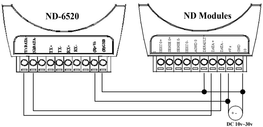
![ND-6520\nND Modules\nTX+ DATA-\nTX+\nTX-\nRX+\nRX-\nGp+Vs\n(G)GND\nIEXC 0+\nSENSE 0+\nSENSE 0-\nIEXC 0-\nAIND 0\nDEFAULT\nDATA+\nDATA-\n+Vs\nGND\n1.0\nDC 10v~30v](.nudam-6000-50m-00083-1000-31/002073a821aa4abeac910db48d367ce8d6c0f493e02c504aa8eba57188c5cf56.jpg)

Figure A-1. ND-60xx Default Setting External Connection
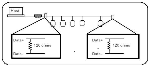
![This diagram illustrates a bus topology.\n\n**Labeled Blocks:**\n*   **Host**: A rectangular block at the top left.\n*   **Left Inset Box**: A large rectangle detailing the termination on the left side. Inside, it lists:\n    *   'Data+'\n    *   '120 ohms' (next to a resistor symbol)\n    *   'Data-'\n*   **Right Inset Box**: A large rectangle detailing the termination on the right side. Inside, it lists:\n    *   'Data+'\n    *   '120 ohms' (next to a resistor symbol)\n    *   'Data-'\n\n**Connections:**\n*   The **'Host'** block connects to a horizontal bus line.\n*   The bus line features multiple vertical drop connections (nodes) along its length.\n*   The leftmost node on the bus connects to the **Left Inset Box**, showing that 'Data+' and 'Data-' lines are terminated by a resistor labeled **'120 ohms'**.\n*   The rightmost node on the bus connects to the **Right Inset Box**, similarly showing 'Data+' and 'Data-' lines terminated by a resistor labeled **'120 ohms'**.](.nudam-6000-50m-00083-1000-31/f189f5c008d32c003b0547d6ba66c61bc70248a72c09fe3569637abb9d822410.jpg)

Figure A-2 Terminator Connection

# Software Utility

# 1.Software Installation

1. Insert “ADLink All-in-one CD” into your CDROM driver.
2. Move cursor on NuDAM and click.
3. Move cursor on NuDAM 6000 Admin Utility and click.
4. Select the driver you want to install and follow the setup instructions on screen.

# 2.How to Execute the NuDAM Administration

# What environment you needed ?

♦ At least one RS-232 communication port.
♦ Microsoft Windows(version 3.1, 95/98/NT)
♦ At least 2MB Hard Drive Space
A VGA monitor(optional)
♦ Mouse (optional)

# Execute the NuDAM Administration Utility

 Run “NuDAM Administration Utility” Icon.

# 3.NuDAM Administration Function Overview

# Default RS-232 Communication Port Setting.

 Communication Port : COM2
Baud Rate 9600
Data Bits 8
Stop Bits 1
 Parity : None

# 3.1 Change RS-232 Communication Port Setting.
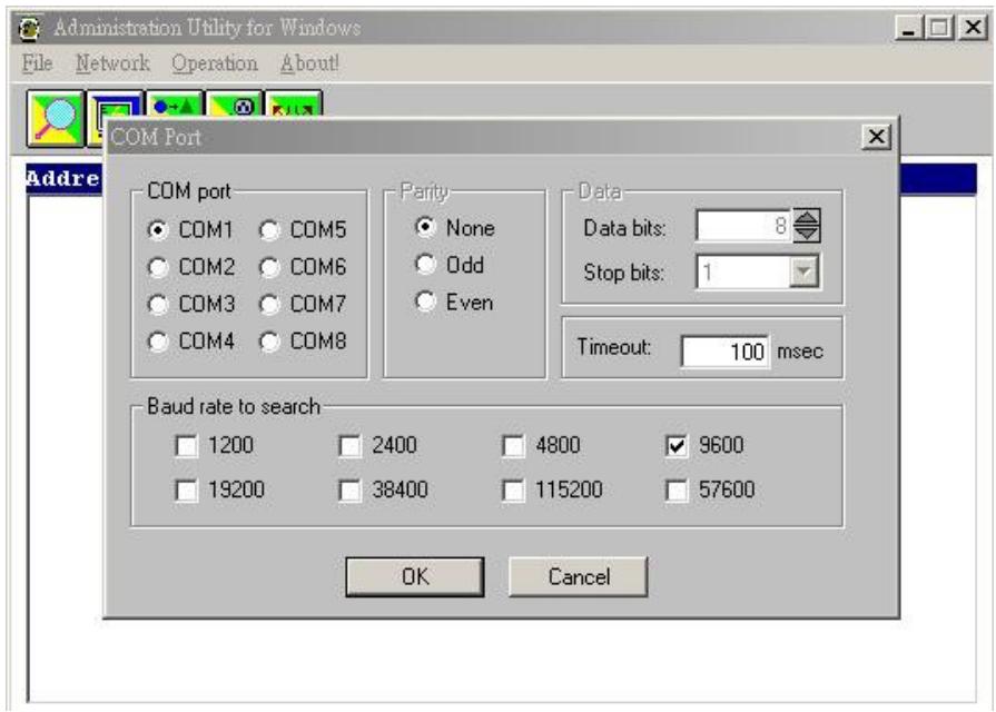
![Administration Utility for Windows\nFile  Network  Operation  About!\nCOM Port\nAddre\nCOM port\nCOM1  COM5\nCOM2  COM6\nCOM3  COM7\nCOM4  COM8\nParity\nNone\nOdd\nEven\nData\nData bits: 8\nStop bits: 1\nTimeout: 100 msec\nBaud rate to search\n1200  2400  4800  9600\n19200  38400  115200  57600\nOK  Cancel](.nudam-6000-50m-00083-1000-31/2274c77e6e935e4ffc040816ad9fc7d95a4da2420c33682c59a7a0becea6c938.jpg)

Choose “Network-ComPort” to change setting.

# 3.2 Search all exist Nudam modules

Choose “Network-Search” to search all exist Nudam modules in the current RS-485 network.
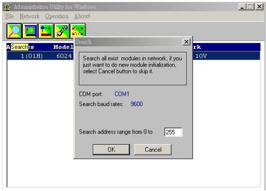
![Administration Utility for Windows\nFile  Network  Operation  About!\nA Search: s  Model\n1 (01H)  6024\nSearch\nSearch all exist modules in network, if you\njust want to do new module initialization,\nselect Cancel button to skip it.\nCOM port:  COM1\nSearch baud rates:  9600\nSearch address range from 0 to  255\nOK  Cancel\nrk\n10V](.nudam-6000-50m-00083-1000-31/ad6b5040bbc648534497a91eeaef2152b8c172973142ab488ca410b21acd2d26.jpg)

# 3.3 Using Operations

Operation-Terminal :

Operation-Configuration :

Operation-Monitor:

Operation-Diagnostic:

Operation-Calibration:

Operation-Model Number:

Terminal Emulation, user can input command and get response message.

Select one exist NuDAM module and select Configuration to do this module‘s common and private setting .

Monitor all the module’s function on the network.

Diagnostic module‘s function.

Some A/D modules need docalibration

Select Model Number
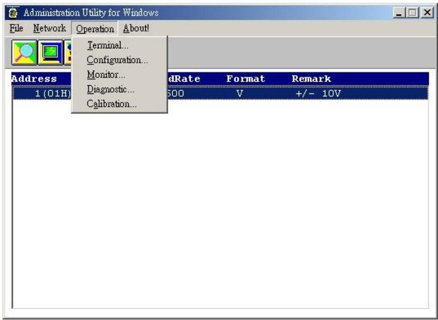
![Administration Utility for Windows\nFile Network Operation About!\nTerminal...\nConfiguration...\nMonitor...\nDiagnostic...\nCalibration...\ndRate	Format	Remark\n1 (01H)	500	V	+/- 10V](.nudam-6000-50m-00083-1000-31/c4a72b31f8ff0a4449d5da5e1597b33783e0f3e6e7908fd1718895a79ef4b899.jpg)

Term

ICON for Operation-Terminal

You can remote control all moudles by directly using command mode, or testing your modules from this Terminal.
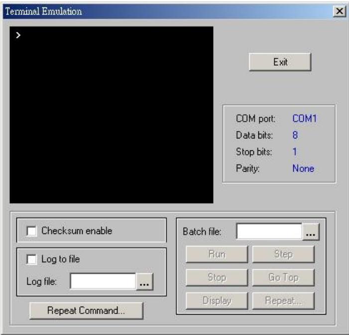
![Terminal Emulation\nExit\nCOM port: COM1\nData bits: 8\nStop bits: 1\nParity: None\nChecksum enable\nLog to file\nLog file: ...\nRepeat Command...\nBatch file:\nRun Step\nStop Go Top\nDisplay Repeat...](.nudam-6000-50m-00083-1000-31/43943bb92588d905b44ea5cc1447ca5f4a2d094d3447ac44409bb8e8cfa29f03.jpg)

Operation-Run Batch Run batch command file in BATCH.CMD user can edit this text file. Operation-Step Batch Run the batch command step by step. Operation-Display Batch:Display content of BATCH.CMD Operation-Repeat Repeat one command n times

Diag ICON for Operation-Diagnostic

This dialog is different by different-fuction modules.
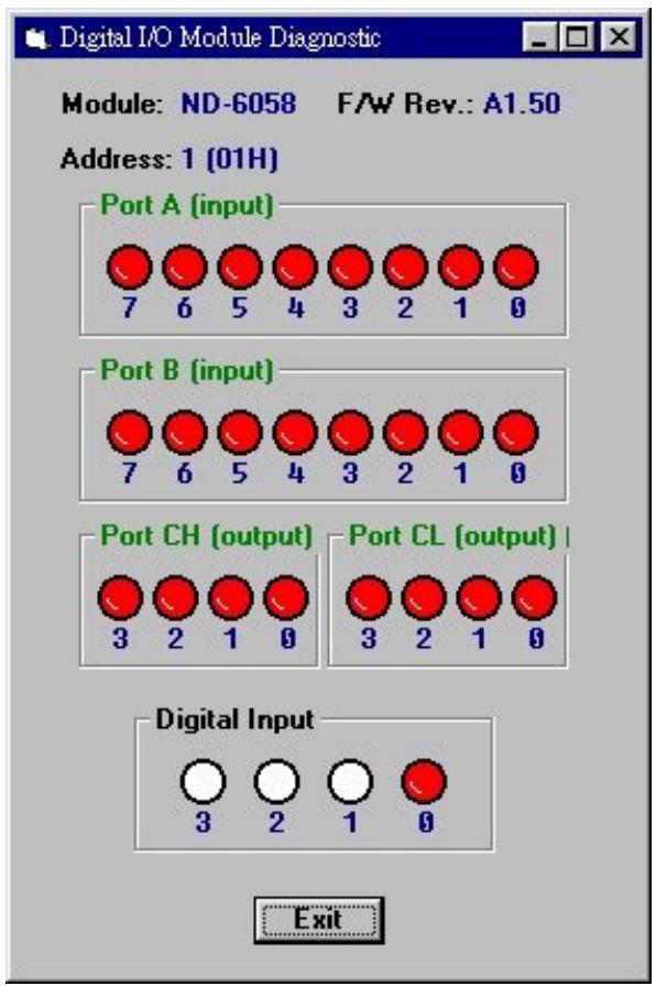
![Digital I/O Module Diagnostic\nModule: ND-6058 F/W Rev.: A1.50\nAddress: 1 (01H)\nPort A (input)\n7 6 5 4 3 2 1 0\nPort B (input)\n7 6 5 4 3 2 1 0\nPort CH (output)\n3 2 1 0\nPort CL (output)\n3 2 1 0\nDigital Input\n3 2 1 0\nExit](.nudam-6000-50m-00083-1000-31/5587cfddf650cc948f37204bcfb2f31a2fe90bc17c5d26dd0adb7d64315db4b1.jpg)

Cal ICON for Operation-Calibration

This dialog is different by different-fuctionmodules.
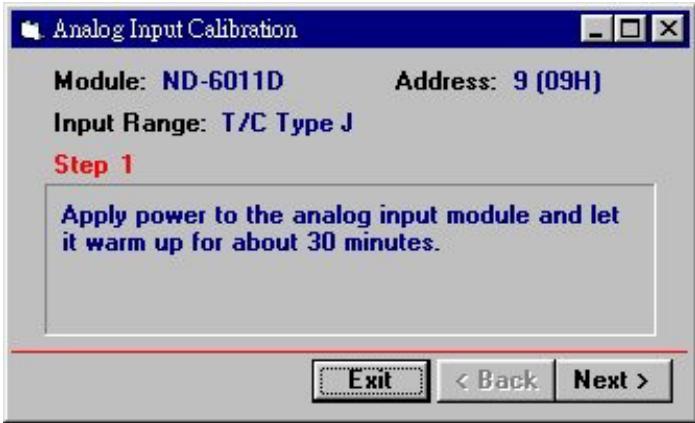
![Analog Input Calibration\nModule: ND-6011D Address: 9 (09H)\nInput Range: T/C Type J\nStep 1\nApply power to the analog input module and let it warm up for about 30 minutes.](.nudam-6000-50m-00083-1000-31/5eb4bb22939b91c58e9b7970c378b9cf047aa2efd057724354da54b0430ae6d9.jpg)

![Analog Input Calibration\nModule: ND-6011D Address: 9 (09H)\nInput Range: T/C Type J\nStep 2\nAssure that the module is correctly installed and\nthe input range shown above is what you want\nto calibrate.](.nudam-6000-50m-00083-1000-31/23e2a12ce347910d2056fea32633ae546f05b59fdeb1a6960f8ef84679a3fcdd.jpg)

# 3.4 Save and Print Nudam modules’ information

File-Save : Save all exist NuDAM modules information as display as in the listbox in the current RS-485 network.

File-Print : Print the NuDAM module information in the listbox.

File-Exit : Quit the NuDAM Administration Utility.
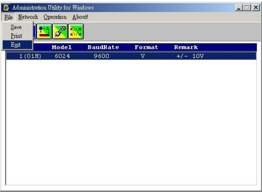
![Administration Utility for Windows\nFile Network Operation About!\nSave\nPrint\nExit\nModel BaudRate Format Remark\n1 (01H) 6024 9600 V +/- 10V](.nudam-6000-50m-00083-1000-31/b8c706f814dcbe4edcb02a402a9d85c6942be16a350ff45fda074eea2bf4d647.jpg)

# 3.5 Version Information

Help-About

Version information
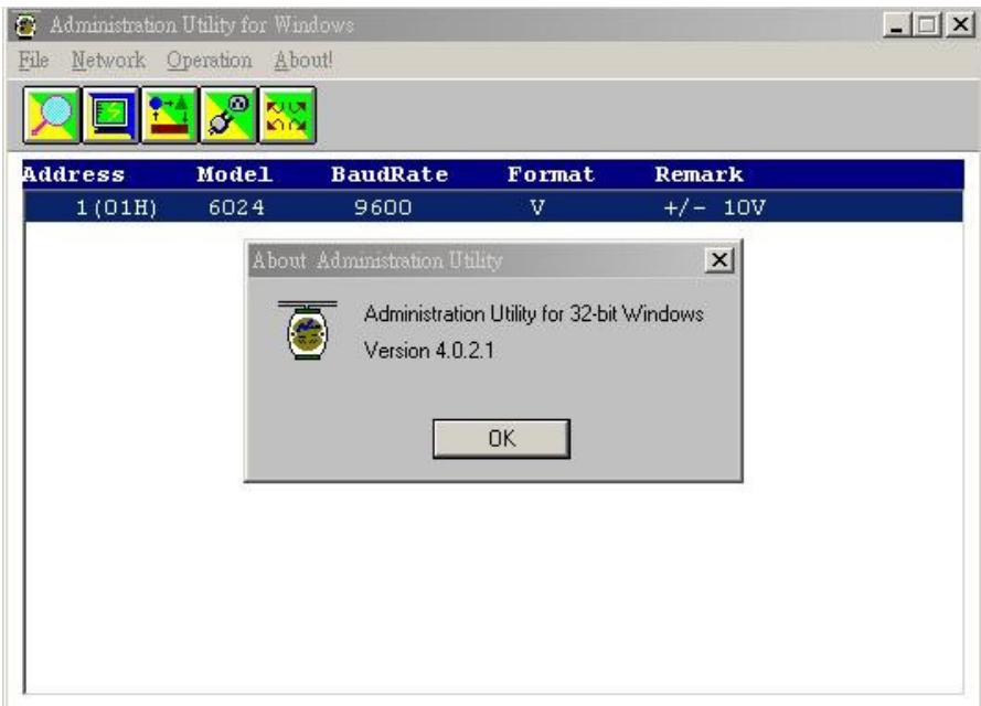
![Administration Utility for Windows\nFile  Network  Operation  About!\nAddress  Model  BaudRate  Format  Remark\n1 (01H)  6024  9600  V  +/-  10V\nAbout Administration Utility\nAdministration Utility for 32-bit Windows\nVersion 4.0.2.1\nOK](.nudam-6000-50m-00083-1000-31/5927231832a0cad027a7e05d51366412b563575e828213dcfac1c189e418ccd6.jpg)

# Safety Instructions

Read and follow all instructions marked on the product and in the documentation before you operate your system. Retain all safety and operating instructions for future use.

Please read these safety instructions carefully.
• Please keep this User‘s Manual for later reference.
Read the specifications section of this manual for detailed information on the operating environment of this equipment.
When installing/mounting or uninstalling/removing equipment, turn off the power and unplug any power cords/cables.
• To avoid electrical shock and/or damage to equipment:

 Keep equipment away from water or liquid sources.
Keep equipment away from high heat or high humidity.
 Keep equipment properly ventilated (do not block or cover ventilation openings).
 Make sure to use recommended voltage and power source settings.
Always install and operate equipment near an easily accessible electrical socketoutlet.
Secure the power cord (do not place any object on/over the power cord).
Only install/attach and operate equipment on stable surfaces and/or recommended mountings.
If the equipment will not be used for long periods of time, turn off and unplug the equipment from its power source.

Never attempt to fix the equipment. Equipment should only be serviced by qualified personnel.

# Getting Service

Ask an Expert: http://askanexpert.adlinktech.com

# ADLINK Technology, Inc.

Address: No. 66, Huaya 1st Rd., Guishan District, Taoyuan City 333411, Taiwan

Tel: +886-3-216-5088

Fax: +886-3-328-5706

Email: service@adlinktech.com

# Ampro ADLINK Technology, Inc.

Address: 6450 Via Del Oro San Jose, CA 95119-1208, USA

Tel: +1-408-360-0200

Toll Free: +1-800-966-5200 (USA only)

Fax: +1-408-600-1189

Email: info@adlinktech.com

# ADLINK Technology (China) Co., Ltd.

Address: 300 Fang Chun Rd., Zhangjiang Hi-Tech Park, Pudong New Area Shanghai, 201203 China

Tel: +86-21-5132-8988

Fax: +86-21-5132-3588

Email: market@adlinktech.com

# ADLINK Technology GmbH

Address: Hans-Thoma-Straße 11

D-68163 Mannheim, Germany

Tel: +49-621-43214-0

Fax: +49-621 43214-30

Email: germany@adlinktech.com

Please visit the Contact page at www.adlinktech.com for information on how to contact the ADLINK regional office nearest you.
[🔗 Link to the original document](.nudam-6000-50m-00083-1000-31/nudam-6000-50m-00083-1000-31.pdf)