# OSM-IMX8MP

User’s Guide

![The image displays a logo featuring the text 'NXP' in a bold, sans-serif typeface. The letters are capitalized and have rounded corners. From left to right, the letters are colored yellow, blue, and green respectively. The letters are arranged horizontally and appear to overlap one another slightly against a plain white background.](.osm-imx8mp-prelim-manual-50m-76100-1000-01/c48b7fb1b0a87eb4bbba9ce9ea836635802bf2a82108110df220b3547226b589.jpg)

![SKHYAN\nHNRNKNKCML\nHRMNE 180A\nADLINK\nZS02114\n#1 STIN470.\n271\n03\nP6A9450C\nMADE IN TAIWAN\nN9300170ZAB7MIESMOLMBP020](.osm-imx8mp-prelim-manual-50m-76100-1000-01/9b0f832a6e4c6cd1f465db78cd0381c0306bfec0b5fb14668e427d32033753a5.jpg)

![The image displays a square icon with rounded corners, likely a logo or app icon. The upper section features a large black zero (0) centered between two thick square brackets. The bracket on the left is magenta, and the bracket on the right is yellow. Below this graphic is a stylized icon of a stack of papers, showing a white top sheet and a grey bottom sheet. The background is white.](.osm-imx8mp-prelim-manual-50m-76100-1000-01/b2cf028c628ccebc188668d11bb0eba0665e6acc830d103c193266467389b1f9.jpg)

OPEN

STANDARD

MODULE TM

Revision: Rev. 0.1 Preliminary

Date: 2024-05-30

Part Number: 50M-76100-1000

![This vertical image features the white Starfleet insignia centered on a red background with a subtle diagonal striped texture. The logo is a stylized arrowhead with three horizontal lines across its upper section. A small registered trademark symbol (®) is visible in the bottom right corner.](.osm-imx8mp-prelim-manual-50m-76100-1000-01/6e6c54f651cbfac876ea377b5a426f2424fabc3aa194cf5786b2eb0f4cee8da5.jpg)

ADLINK

LEADING EDGE COMPUTING

Revision History

<table><tr><td>Revision</td><td>Description</td><td>Date</td><td>Author</td></tr><tr><td>0.1</td><td>Preliminary release</td><td>2024-05-30</td><td>AL</td></tr></table>

# Preface

# Disclaimer

Information in this document is provided in connection with ADLINK products. No license, express or implied, by estoppel or otherwise, to any intellectual property rights is granted by this document. Except as provided in ADLINK´s Terms and Conditions of Sale for such products, ADLINK assumes no liability whatsoever, and ADLINK disclaims any express or implied warranty, relating to sale and/or use of ADLINK products including liability or warranties relating to fitness for a particular purpose, merchantability, or infringement of any patent, copyright or other intellectual property right. If you intend to use ADLINK products in or as medical devices, you are solely responsible for all required regulatory compliance, including, without limitation, Title 21 of the CFR (US), Directive 2007/47/EC (EU), and ISO 13485 & 14971, if any. ADLINK may make changes to specifications and product descriptions at any time, without notice.

# Environmental Responsibility

ADLINK is committed to fulfil its social responsibility to global environmental preservation through compliance with the European Union's Restriction of Hazardous Substances (RoHS) directive and Waste Electrical and Electronic Equipment (WEEE) directive. Environmental protection is a top priority for ADLINK. We have enforced measures to ensure that our products, manufacturing processes, components, and raw materials have as little impact on the environment as possible. When products are at their end of life, our customers are encouraged to dispose of them in accordance with the product disposal and/or recovery programs prescribed by their nation or company.

![The image displays a black and white graphic. At the top, there is a line drawing of a wheeled trash bin with a lid. A large black 'X' is superimposed over the bin, crossing it out. Below the bin, there is a solid black rectangular bar.](.osm-imx8mp-prelim-manual-50m-76100-1000-01/ffe030a0b3913065e6068de0fb2e6e95722cd9461cced0aac04d7ecaed2393c5.jpg)

![The image displays a yellow triangular warning sign with a thick black border. Inside the triangle is a black exclamation point. The sign is centered on a white background.](.osm-imx8mp-prelim-manual-50m-76100-1000-01/eba50573a84b1a2938083d26db2ad09be38854cf13c19012cbd3f61ff874723d.jpg)

California Proposition 65 Warning: This product can expose you to chemicals including acrylamide, arsenic, benzene, cadmium, Tris(1,3- dichloro-2-propyl)phosphate (TDCPP), 1,4-Dioxane, formaldehyde, lead, DEHP, styrene, DINP, BBP, PVC, and vinyl materials, which are known to the State of California to cause cancer, and acrylamide, benzene, cadmium, lead, mercury, phthalates, toluene, DEHP, DIDP, DnHP, DBP, BBP, PVC, and vinyl materials, which are known to the State of California to cause birth defects or other reproductive harm. For more information go to www.P65Warnings.ca.gov.

# Trademarks

Product names mentioned herein are used for identification purposes only and may be trademarks / registered trademarks of respective companies.

# Copyright © 2024 ADLINK Technology Incorporated

This document contains proprietary information protected by copyright. All rights are reserved. No part of this manual may be reproduced by any mechanical, electronic, or other means in any form without prior written permission of the manufacturer.

# Safety Instructions

For user safety, please read and follow all Instructions, WARNINGs, CAUTIONs, and NOTEs marked in this manual and on the associated equipment before handling/operating the equipment.

Read these safety instructions carefully.

Keep this manual for future reference.
• Read the specifications section of this manual for detailed information on the operating environment of this equipment.
• Turn off power and unplug any power cords/cables when installing/mounting or un-installing/removing equipment.
• To avoid electrical shock and/or damage to equipment:
Keep equipment away from water or liquid sources;
Keep equipment away from high heat or high humidity;
• Keep equipment properly ventilated (do not block or cover ventilation openings);
• Make sure to use recommended voltage and power source settings;
• Always install and operate equipment near an easily accessible electrical socket outlet;
• Secure the power cord (do not place any object on/over the power cord);
• Only install/attach and operate equipment on stable surfaces and/or recommended mountings;
• If the equipment will not be used for long periods of time, turn off the power source and unplug the equipment.

# Conventions

The following conventions may be used throughout this manual, denoting special levels of information.

![The image displays a red icon resembling a square document or page with a slightly rounded bottom-right corner. Inside the outline, there are three horizontal lines stacked vertically.](.osm-imx8mp-prelim-manual-50m-76100-1000-01/d174cd0781470e373faddef6d5b954acea0dca63cde2ff21cd87c5a4e6badacc.jpg)

Note: This information adds clarity or specifics to text and illustrations.

![The image displays a pixelated, yellow, upward-pointing triangular warning sign with a white exclamation mark centered inside it.](.osm-imx8mp-prelim-manual-50m-76100-1000-01/806b280be312ce6e8ffb4709d29e668a5c6c70fbc9f5e1a6c77c30218c6d36a3.jpg)

Caution: This information indicates the possibility of minor physical injury, component damage, data loss, and/or program corruption.

![This image displays a standard warning symbol: a red triangle with rounded corners containing a white exclamation mark in the center.](.osm-imx8mp-prelim-manual-50m-76100-1000-01/cf60242657cd28f199526ca4861e99eb329474bdb96c1fb5f3f1e288993b454b.jpg)

Warning: This information warns of possible serious physical injury, component damage, data loss, and/or program corruption.

# Getting Service

Ask an Expert: https://www.adlinktech.com/en/Askanexpert

# ADLINK Technology, Inc.

No. 66, Huaya 1st Rd., Guishan District, Taoyuan City 333411, Taiwan

Tel: +886-3-216-5088

Fax: +886-3-328-5706

Email: service@adlinktech.com

# Ampro ADLINK Technology, Inc.

6450 Via Del Oro, San Jose, CA 95119-1208, USA

Tel: +1-408-360-0200

Toll Free: +1-800-966-5200 (USA only)

Fax: +1-408-600-1189

Email: info@adlinktech.com

# ADLINK Technology (China) Co., Ltd.

300 Fang Chun Rd., Zhangjiang Hi-Tech Park, Pudong New Area, Shanghai, 201203, China

Tel: +86-21-5132-8988

Fax: +86-21-5132-3588

Email: market@adlinktech.com

# ADLINK Technology GmbH

Hans-Thoma-Strasse 11, D-68163 Mannheim, Germany

Tel: +49-621-43214-0

Fax: +49-621 43214-30

Email: emea@adlinktech.com

Please visit the Contact page at www.adlinktech.com for information on how to contact the ADLINK regional office nearest you.

# Table of Contents

Revision History ..

Preface ..

List of Figures ... . 8

1. Introduction .. C

1.1. The OSM Form factor .... . 9

2. Specifications... .10

2.1. Core System.... ..10

2.2. Video .... ..11

2.2.1 GPU ... ..11

2.2.2 Display Interface Support . ..11

2.3. Camera... ... 12

2.4. Audio ... ..12

2.5. Dual Wired Ethernet . ..12

2.6. Expansion Busses .. ..13

2.7. System Storage.... ..14

2.8. Program Header.... ..14

2.9. FAN Control .. ..14

2.10. Power... ... 15

2.11. Mechanical and Environmental.... ..15

3. Block Diagram... .17

4. Pinout and Signal Descriptions .... .18

4.1. Pin Summary... ..18

4.2. Signal Terminology Descriptions .. ..20

4.3. Signal Description by Function .. ..21

4.3.1 LVDS Display Interface.. ..21

4.3.2 MIPI Camera Support.. ..24

4.3.3 Audio Interfaces . ..25

4.3.4 USB Ports ... ..26

4.3.5 PCIe.. ..29

4.3.6 Dual LAN ports .. ..30

4.3.7 SDIO Card (4-bit) . ..32

4.3.8 SPI Interfaces . ..35

4.3.9 GPIO.. .... 36

4.3.10 CAN Bus .. ..37

4.3.11 ADC... ..37
4.3.12 Power + Boot Select . ..37

5. Software Support... ..42

5.1. Early Access. ..42
5.2. Yocto... ..42

6. Mechanical.... ..43

6.1. Module Dimensions.... ..43

7. Thermal Solutions... ..44

7.1. Heatspreader : HTS.. ..44
7.2. Heatsink: THS .. ..44
..44

# List of Figures

Figure 1 – Module function diagram... 17
Figure 2 – Module size grid.... .18
Figure 3 – Module pinout grid ............. ..19
Figure 4 – Placement area and Cut-out area – size L.. ..43

# 1. Introduction

# 1.1. The OSM Form factor

The OSM (“Open Standard Module™”) specification allows the development, production, and distribution of embedded modules for the most popular MCU32, ARM and x86 architectures. For a growing number of IoT applications, this standard helps combine the advantages of modular embedded computing with increasing requirements for costs, space, and interfaces.

The modules are used as building blocks for portable and stationary embedded systems. They consist of the core CPU and support circuits, including DRAM, boot flash, power sequencing, CPU power supplies. The modules are employed with application-specific carrier boards that implement other features such as audio CODECs, touch controllers, wireless devices, PHY’s, and other related features. This modular approach allows for scalability, fast time to market, and upgradability while still maintaining low costs, low power consumption, and small physical size.

![The image features a logo on the left and text on the right. The logo consists of large lime green letters 'S', 'G', and 'T', with a small magenta circle containing a lowercase white 'e' positioned between the 'G' and 'T'.\n\nThe text on the right reads:\nSTANDARDIZATION\nGROUP FOR\nEMBEDDED\nTECHNOLOGIES\n\nThe words 'STANDARDIZATION', 'GROUP FOR', and 'TECHNOLOGIES' are in black, while the word 'EMBEDDED' is in magenta.](.osm-imx8mp-prelim-manual-50m-76100-1000-01/d90803ec499e59dcd5a24a4b2184d1707b3abdcef616389c9a60bdfaaeff423e.jpg)

OSM module and carrier specifications are available online at: https://sget.org/standards/osm/

# 2. Specifications

# 2.1. Core System

# CPU

4x / 2x ARM Cortex-A53 @ | 1x Cortex M7 | 2.3 TOPS NPU

ARM Cortex-A53 MP Core processors are high-performance and optimized for low power.

# Memory

The chip has a single 32-bit DRAM controller.

• LPDDR4, soldered down
• 32-bit DRAM interface

# L2 Cache

512KB system L2 cache

# Security

Arm® TrustZone® EdgeLock® secure enclave

# 2.2. Video

# 2.2.1 GPU

GPU Core

Vivante GC7000UL

# Graphics Feature Support

GC7000UL (2 shaders), OpenGL ES 2.0/3.0/3.1,

Vulkan, OpenCL 1.2; GC380 (2D)

# 2.2.2 Display Interface Support

MIPI DSI

1x MIPI DSI 4 lane Compliant to MIPI-DSI standard v1.2

Maximum resolution 1080p60 with 24-bit RGB

# LVDS

2-channel LVDS port, up to 1920x1080p60 resolution

# HDMI

HDMI 2.0a complaint, up to 1920x1080p60 / 3840x2160p30

# 2.3. Camera

One 4-lane MIPI CSI2 camera input

# 2.4. Audio

I2S to carrier

# 2.5. Dual Wired Ethernet

# Primary LAN

MAC 10/100/1000 Ethernet Controller on SoC

Supports 10/100/1000-Mbps data transfer rates, both full-duplex and half-duplex

# Secondary LAN

MAC 10/100/1000 Ethernet Controller on SoC

Supports 10/100/1000-Mbps data transfer rates, both full-duplex and half-duplex

# 2.6. Expansion Busses

USB: 2x USB 2.0, 2x USB 3.0

UART: 4 UART interfaces

CANbus: 2x CAN Supports CAN FD mode, data bit rate up to 8 Mbps

SPI: 2x SPI

I2S: 1x I2S interface with audio resolution from 16-bits to 32-bits and sample rate up to 192KHz (see Audio Codec support)

ADC: 2x ADC

PWM: 4x PWM

I2C: 2x I2C interfaces

• Support 7-bit mode
• Software programmable clock frequency of 100 kbit/s in Standard-mode, 400 kbit/s in Fast-mode, or 1 Mbit/s in Fast-mode Plus.

GPIO: 8x GPIO

# 2.7. System Storage

# SDIO

2x SDIO (4-bit), compatible with SD3.0

# eMMC

32, 64, 128 GB (built-in storage options)

# 2.8. Program Header

JTAG solder points

# 2.9. FAN Control

None, only passive cooling is needed.

# 2.10. Power

# Power Modes

ON / OFF / SUSPEND

Power on / off behavior same as x86 AT (always boot)

# Voltage Input

5.0V +/- 5%

# Operating Temperatures (vs power input)

Standard Operating Temperature: 0 to 60°C

Extreme Rugged Operating Temperature: -40 to 85°C

Commercial grade BOM (memory, eMMC, SOC)

Industrial grade BOM (memory, eMMC, SOC)

# 2.11. Mechanical and Environmental

# Form Factor and Specification

OSM R1.1 Size-L

# Environmental Humidity

Derating for two different BOMs

• 5-90% RH operating, non-condensing
• 5-95% RH storage (and operating with conformal coating)

# EMI

EN55022 Class B inside an enclosure

# Shock and Vibration

HALT Testing, including test report confirming extended operating

temperature range during and after vibration. A separate

shock test report to MIL-STD-202F, Method 213B, Table 213-I, Condition A.

IN ADDITION: When installed on a baseboard, the device shall operate under 18 sawtooth mechanical shocks

(3 shocks in each direction) with a peak acceleration of 40g for a duration of 18 msec each and 75g for a duration of 6 msec each.

Capable of supporting random vibration: MIL-STD-202F, Method 214A, Table 214-I, Condition D. If HALT testing shows equal or better performance, a separate vibration test report is not necessary.

# MTBF

300,000 hrs. (at 40°C), 100,000 hrs. (at 85°C)

Two different BOM: 0-60°C and -40-85°C

# 3. Block Diagram

![The diagram centers on a large reddish block labeled **NXP i.MX8M plus** and **OSM L**. Connections radiate outward to various peripheral blocks.\n\n**Top Connections:**\n*   **eMMC 5.1 32/64/128 GB** connects to the top of the central block.\n*   **LPDDR4 2/4/8 GB** connects to the top of the central block.\n\n**Left Side Connections (External to Central):**\n*   **DSI 4L** connects to port **DSI 4L**.\n*   **LVDS 8L** connects to port **LVDS**.\n*   **eDP_A** connects to port **HDMI**.\n*   **CSI 4L** connects to port **CSI**.\n*   **ETH_A** connects to port **RGMII_0**.\n*   **ETH_B** connects to port **RGMII_1**.\n*   **USB_D** connects to port **USB_1** (labeled **OTG**).\n*   **USB_A**, **USB_B**, and **USB_C** connect to a blue block labeled **USB hub**, which then connects to port **USB_2**.\n*   **I2S_A** connects to port **SAI**.\n*   **SPI_A** connects to port **ECSPI_1**.\n*   **SPI_B** connects to port **ECSPI_2**.\n\n**Right Side Connections (External to Central):**\n*   Port **UART_2** connects to **Console**.\n*   Port **UART_1** connects to **UART_A 4w**.\n*   Port **UART_4** connects to **UART_B 4w**.\n*   Port **UART_3** connects to **UART_C 2w**.\n*   Port **I2C_1** connects to **I2C_A**.\n*   Port **I2C_2** connects to **I2C_B**.\n*   Port **GPIO** connects to **GPIO_A**.\n*   Port **CAN_1** connects to **CAN_A**.\n*   Port **CAN_2** connects to **CAN_B**.\n*   Port **SD_1** connects to **SDIO_A**.\n*   Port **SD_2** connects to **SDIO_B**.\n*   A port at the bottom right connects to a yellow block labeled **JTAG**.\n\n**Bottom Connections:**\n*   Port **I2C** connects to a blue block labeled **MCU**.\n*   From **MCU**, a line labeled **X4** connects to **PWM**.\n*   From **MCU**, a line labeled **x2** connects to **ADC**.](.osm-imx8mp-prelim-manual-50m-76100-1000-01/ea6adb29f2f89afa339a3d9101b85eee0dfd3f46b31e67f7fc13c8251c3249c5.jpg)

Figure 1 – Module function diagram

# 4. Pinout and Signal Descriptions

# 4.1. Pin Summary

Size-0 -“Zero": 30 mm x 15 mm
Size-S- "Small": 30 mm x 30 mm
Size-M-“Medium": 30 mm x 45 mm
Size-L-“Large": 45 mm x 45 mm

![45 mm\n30 mm\n45 mm](.osm-imx8mp-prelim-manual-50m-76100-1000-01/f17d867860d5193aa14f0ca1e8b3b1f5edeb68c940b15614607b04753eeaddaf.jpg)

Figure 2 – Module size grid

![2 4 6 8 10 12 14 16 18 20 22 24 26 28 30 32 34\n1 3 5 7 9 11 13 15 17 19 21 23 25 27 29 31 33 35\nA —○○○○○○○○○○○○○○○○○○○○○○○○○○○○○○○○○○○○○○○○○○○○○○○○○○○○○○○○○○○○○○○○○○○○○○○○○○○○○○○○○○○○○○○○○○○○○○○○○○○○\nB —— ○●●●●●●●●●●●●●●●●●●●●●●●●●●●●●●●●●●●●●●●●●●●●●●●\nC —— ○●●●●●●●●●●●●●●●●●●●●●●●●●●●●●●●●●●●●●●●●●●\nD —— ○●●●●●●●●●●●●●●●●●●●●●●●●●●●●●●●●●●●●●\nE —— ○●●●——\nF —— ○●●●——\nG —— ○●●●——\nH —— ○●●●——\nJ —— ○●●●——\nK —— ○●●●——\nL —— ○●●●——\nM —— ○●●●——\nN —— ○●●●——\nP —— ○●●●——\nR —— ○●●●——\nT —— ○●●●——\nU —— ○●●●——\nV —— ○●●●——\nW —— ○●●●——\nY —— ○●●●——\nAA —— ○●●●——\nAB —— ○●●●——\nAC —— ○●●●——\nAD —— ○●● ●——\nAE —— ○ ●——\nAF —— ○ ●——\nAG —— ○ ●——\nAH —— ○ ●——\nAJ —— ○ ●——\nAK —— ○ ●——\nAL —— ○ ●——\nAM —— ○ ●——\nAN —— ○ ●——\nAP —— ○ ●——\nAR —— ○ ●——](.osm-imx8mp-prelim-manual-50m-76100-1000-01/fd8fcc5ac1386515d27517feb719fcafd288424696a4fc222ecbf4c76331df31.jpg)

Figure 21: Contact Grid (all sizes) (view from top, through the module)
Figure 3 – Module pinout grid

# 4.2. Signal Terminology Descriptions

The following information provides descriptions of the terms used in the signal description table:

<table><tr><td>Term</td><td>Description</td></tr><tr><td>I</td><td></td></tr><tr><td>O</td><td></td></tr><tr><td>I/O</td><td></td></tr><tr><td>OD</td><td></td></tr><tr><td>PU</td><td></td></tr><tr><td>PD</td><td></td></tr><tr><td>CMOS</td><td></td></tr><tr><td>GBE MDI</td><td></td></tr><tr><td>DP</td><td></td></tr><tr><td>D-PHY</td><td></td></tr><tr><td>M-PHY</td><td></td></tr><tr><td>LVDS</td><td></td></tr><tr><td>PCIE</td><td></td></tr><tr><td>SATA</td><td></td></tr><tr><td>TMDS HDMI</td><td></td></tr><tr><td>USB</td><td></td></tr><tr><td>USB SS</td><td></td></tr><tr><td>USB VBUS 5V</td><td></td></tr><tr><td>VDD_IN</td><td></td></tr><tr><td>3.3V</td><td></td></tr><tr><td>1.8V</td><td></td></tr><tr><td>3.3Vsb</td><td></td></tr><tr><td>1.8Vsb</td><td></td></tr><tr><td>Sleep</td><td></td></tr><tr><td>Runtime</td><td></td></tr><tr><td></td><td></td></tr></table>

# 4.3. Signal Description by Function

# 4.3.1 LVDS Display Interface

For information on LVDS support for a single-channel with 4 lanes, please refer to the details below:

<table><tr><td>Contact Name</td><td>Contact Acronym</td><td>Functional Description</td><td>I/O Type</td><td>I/O Level</td><td>PU / PD</td><td>Comments</td></tr><tr><td>LVDS_I2C_CLK</td><td>AM11</td><td>DDC clock line used for flat panel detection and control</td><td>O OD CMOS</td><td>1.8V</td><td>PU 2k2</td><td></td></tr><tr><td>LVDS_I2C_DAT</td><td>AM12</td><td>DDC data line used for flat panel detection and control</td><td>I/O OD CMOS</td><td>1.8V</td><td>PU 2k2</td><td></td></tr><tr><td>LVDS_VDD_EN</td><td>AN14</td><td>LVDS channel power enable, active high</td><td>O CMOS</td><td>1.8V</td><td></td><td></td></tr><tr><td>LVDS_BL_PWM</td><td>AN22</td><td>LVDS channel brightness control through pulse width modulation</td><td>O CMOS</td><td>1.8V</td><td></td><td></td></tr><tr><td>LVDS_BL_EN</td><td>AN23</td><td>LVDS channel backlight enable, active high</td><td>O CMOS</td><td>1.8V</td><td></td><td></td></tr><tr><td>LVDS_A_CLK_P</td><td>AN13</td><td>LVDS channel A differential pair clock lines</td><td>O LVDS LCD</td><td></td><td></td><td></td></tr><tr><td>LVDS_A_CLK_N</td><td>AN12</td><td>LVDS channel A differential pair clock lines</td><td>O LVDS LCD</td><td></td><td></td><td></td></tr><tr><td>LVDS_A_LANE0_P</td><td>AP18</td><td>LVDS channel A differential pair data lines</td><td>O LVDS LCD</td><td></td><td></td><td></td></tr><tr><td>LVDS_A_LANE0_N</td><td>AP17</td><td>LVDS channel A differential pair data lines</td><td>O LVDS LCD</td><td></td><td></td><td></td></tr><tr><td>LVDS_A_LANE1_P</td><td>AR16</td><td>LVDS channel A differential pair data lines</td><td>O LVDS LCD</td><td></td><td></td><td></td></tr><tr><td>LVDS_A_LANE1_N</td><td>AR15</td><td>LVDS channel A differential pair data lines</td><td>O LVDS LCD</td><td></td><td></td><td></td></tr><tr><td>LVDS_A_LANE2_P</td><td>AP15</td><td>LVDS channel A differential pair data lines</td><td>O LVDS LCD</td><td></td><td></td><td></td></tr><tr><td>LVDS_A_LANE2_N</td><td>AP14</td><td>LVDS channel A differential pair data lines</td><td>O LVDS LCD</td><td></td><td></td><td></td></tr><tr><td>LVDS_A_LANE3_P</td><td>AP12</td><td>LVDS channel A differential pair data lines</td><td>O LVDS LCD</td><td></td><td></td><td></td></tr><tr><td>LVDS_A_LANE3_N</td><td>AP11</td><td>LVDS channel A differential pair data lines</td><td>O LVDS LCD</td><td></td><td></td><td></td></tr></table>

4.3.1.1. DSI0 Mode

<table><tr><td>Contact Name</td><td>Contact Acronym</td><td>Functional Description</td><td>I/O Type</td><td>I/O Level</td><td>PU / PD</td><td>Comments</td></tr><tr><td>DSI_DATA0_N</td><td>AB11</td><td>DSI differential output (point to point)</td><td>O LVDS D-PHY</td><td></td><td></td><td></td></tr><tr><td>DSI_DATA0_P</td><td>AB10</td><td>DSI differential output (point to point)</td><td>O LVDS D-PHY</td><td></td><td></td><td></td></tr><tr><td>DSI_DATA1_N</td><td>AC9</td><td>DSI differential output (point to point)</td><td>O LVDS D-PHY</td><td></td><td></td><td></td></tr><tr><td>DSI_DATA1_P</td><td>AC8</td><td>DSI differential output (point to point)</td><td>O LVDS D-PHY</td><td></td><td></td><td></td></tr><tr><td>DSI_DATA2_N</td><td>AC6</td><td>DSI differential output (point to point)</td><td>O LVDS D-PHY</td><td></td><td></td><td></td></tr><tr><td>DSI_DATA2_P</td><td>AC5</td><td>DSI differential output (point to point)</td><td>O LVDS D-PHY</td><td></td><td></td><td></td></tr><tr><td>DSI_DATA3_N</td><td>AB5</td><td>DSI differential output (point to point)</td><td>O LVDS D-PHY</td><td></td><td></td><td></td></tr><tr><td>DSI_DATA3_P</td><td>AB4</td><td>DSI differential output (point to point)</td><td>O LVDS D-PHY</td><td></td><td></td><td></td></tr><tr><td>DSI_CLOCK_N</td><td>AB8</td><td>DSI differential clock output (point to point)</td><td>O LVDS D-PHY</td><td></td><td></td><td></td></tr><tr><td>DSI_CLOCK_P</td><td>AB7</td><td>DSI differential clock output (point to point)</td><td>O LVDS D-PHY</td><td></td><td></td><td></td></tr><tr><td>DSI_TE</td><td>AA3</td><td>DSI panel tearing effect signal</td><td>I CMOS</td><td>1.8V</td><td></td><td></td></tr><tr><td>DISP_VDD_EN / GPIO_C_4</td><td>F3</td><td>Primary display power enable, active high</td><td>O CMOS</td><td>1.8V</td><td></td><td></td></tr><tr><td>DISP_BL_EN / GPIO_C_5</td><td>F4</td><td>Primary display backlight enable, active high</td><td>O CMOS</td><td>1.8V</td><td></td><td></td></tr><tr><td>DISP_BL_PWM / PWM_0</td><td>E18</td><td>Primary display brightness control through pulse width modulation</td><td>O CMOS</td><td>1.8V</td><td></td><td></td></tr></table>

# 4.3.1.2. eDP0 / eDP1 Mode

N/A

4.3.1.3. HDMI MODE (to eDP A)

<table><tr><td>Contact Name</td><td>Contact Acronym</td><td>Functional Description</td><td>I/O Type</td><td>I/O Level</td><td>PU / PD</td><td>Comments</td></tr><tr><td>eDP_A_LANE0_P</td><td>A30</td><td>Primary 4-lane eDP differential pair data lines</td><td>O LVDS DP</td><td></td><td></td><td>AC coupled off module</td></tr><tr><td>eDP_A_LANE0_N</td><td>A31</td><td>Primary 4-lane eDP differential pair data lines</td><td>O LVDS DP</td><td></td><td></td><td>AC coupled off module</td></tr><tr><td>eDP_A_LANE1_P</td><td>B31</td><td>Primary 4-lane eDP differential pair data lines</td><td>O LVDS DP</td><td></td><td></td><td>AC coupled off module</td></tr><tr><td>eDP_A_LANE1_N</td><td>B32</td><td>Primary 4-lane eDP differential pair data lines</td><td>O LVDS DP</td><td></td><td></td><td>AC coupled off module</td></tr><tr><td>eDP_A_LANE2_P</td><td>A33</td><td>Primary 4-lane eDP differential pair data lines</td><td>O LVDS DP</td><td></td><td></td><td>AC coupled off module</td></tr><tr><td>eDP_A_LANE2_N</td><td>A34</td><td>Primary 4-lane eDP differential pair data lines</td><td>O LVDS DP</td><td></td><td></td><td>AC coupled off module</td></tr><tr><td>eDP_A_LANE3_P</td><td>B34</td><td>Primary 4-lane eDP differential pair data lines</td><td>O LVDS DP</td><td></td><td></td><td>AC coupled off module</td></tr><tr><td>eDP_A_LANE3_N</td><td>B35</td><td>Primary 4-lane eDP differential pair data lines</td><td>O LVDS DP</td><td></td><td></td><td>AC coupled off module</td></tr><tr><td>eDP_A_AUX_P</td><td>C33</td><td>Primary bidirectional eDP channel used for link management and device control</td><td>I/O LVDS DP</td><td></td><td>PD 100k</td><td>AC coupled off module</td></tr><tr><td>eDP_A_AUX_N</td><td>C34</td><td>Primary bidirectional eDP channel used for link management and device control</td><td>I/O LVDS DP</td><td></td><td>PD 100k</td><td>AC coupled off module</td></tr><tr><td>eDP_A_AUX_SEL</td><td>D32</td><td>Strapping signal to enable either HDMI or DP output</td><td>I CMOS</td><td>1.8V</td><td>PD 1M</td><td>Pulled to GND on Carrier for DP operation in dual mode (DP++) implementations. Driven to 1.8V on carrier for HDMI mode module must tolerate high level in stand-by mode.</td></tr><tr><td>eDP_A_BL_HPD</td><td>D33</td><td>Detection of hot plug / unplug of the primary eDP display and notification of the link layer.</td><td>I CMOS</td><td>1.8V</td><td>PD 1M</td><td>Module must tolerate high level in stand-by mode.</td></tr><tr><td>eDP_A_BL_EN</td><td>D31</td><td>Primary eDP panel backlight enabled, active high</td><td>O CMOS</td><td>1.8V</td><td></td><td></td></tr><tr><td>eDP_A_BL_PWM</td><td>C31</td><td>Primary eDP panel brightness control through pulse width modulation</td><td>O CMOS</td><td>1.8V</td><td></td><td></td></tr></table>

# 4.3.1.4. eDP\_B

N/A

# 4.3.2 MIPI Camera Support

4.3.2.1. CSI (4 lanes)

<table><tr><td>Contact Name</td><td>Contact Acronym</td><td>Functional Description</td><td>I/O Type</td><td>I/O Level</td><td>PU / PD</td><td>Comments</td></tr><tr><td>CSI_DATA0_N</td><td>C1</td><td>CSI differential input (point to point)</td><td>I LVDS D-PHY/ I LVDS M-PHY</td><td></td><td></td><td></td></tr><tr><td>CSI_DATA0_P</td><td>B1</td><td>CSI differential input (point to point)</td><td>I LVDS D-PHY / I LVDS M-PHY</td><td></td><td></td><td></td></tr><tr><td>CSI_DATA1_N</td><td>A2</td><td>CSI differential input (point to point)</td><td>I LVDS D-PHY / I LVDS M-PHY</td><td></td><td></td><td></td></tr><tr><td>CSI_DATA1_P</td><td>A3</td><td>CSI differential input (point to point)</td><td>I LVDS D-PHY / I LVDS M-PHY</td><td></td><td></td><td></td></tr><tr><td>CSI_DATA2_N</td><td>A5</td><td>CSI differential input (point to point)</td><td>I LVDS D-PHY / I LVDS M-PHY</td><td></td><td></td><td></td></tr><tr><td>CSI_DATA2_P</td><td>A6</td><td>CSI differential input (point to point)</td><td>I LVDS D-PHY / I LVDS M-PHY</td><td></td><td></td><td></td></tr><tr><td>CSI_DATA3_N</td><td>B6</td><td>CSI differential input (point to point)</td><td>I LVDS D-PHY / I LVDS M-PHY</td><td></td><td></td><td></td></tr><tr><td>CSI_DATA3_P</td><td>B7</td><td>CSI differential input (point to point)</td><td>I LVDS D-PHY / I LVDS M-PHY</td><td></td><td></td><td></td></tr><tr><td>CSI_CLOCK_N</td><td>B3</td><td>CSI differential clock input (point to point)</td><td>I LVDS D-PHY</td><td></td><td></td><td></td></tr><tr><td>CSI_CLOCK_P</td><td>B4</td><td>CSI differential clock input (point to point)</td><td>I LVDS D-PHY</td><td></td><td></td><td></td></tr><tr><td>CAM_MCK</td><td>C2</td><td>Master clock output</td><td>O CMOS</td><td>1.8V</td><td></td><td></td></tr><tr><td>I2C_CAM_SDA / CSI_TX_N</td><td>C3</td><td>I2C data for serial camera data support link or differential data lane</td><td>I/O OD CMOS / O LVDS M- PHY</td><td>1.8V</td><td>PU 2.2K</td><td>MIPI-CSI 2.0 mode uses I2C_CAM_SDAMIPI-CSI 3.0 mode uses CSI_TX_N</td></tr><tr><td rowspan="2">I2C_CAM_SCL / CSI_TX_P</td><td rowspan="2">C4</td><td rowspan="2">I2C clock for serial camera data support link or differential data lane</td><td>I/O OD CMOS</td><td rowspan="2">1.8V</td><td rowspan="2">PU 2.2K</td><td>MIPI-CSI 2.0 mode uses I2C_CAM_SCL</td></tr><tr><td>/ O LVDS M-PHY</td><td>MIPI-CSI 3.0 mode uses CSI_TX_P</td></tr><tr><td>CAM_PWR / GPIO_C_6</td><td>G3</td><td>Camera 0 Power Enable, active high output.</td><td>O CMOS</td><td>1.8V</td><td></td><td></td></tr><tr><td>CAM_RST# / GPIO_C_7</td><td>G4</td><td>Camera 0 reset, active low output</td><td>O CMOS</td><td>1.8V</td><td></td><td></td></tr></table>

# 4.3.3 Audio Interfaces

4.3.3.1. I2S0

<table><tr><td>Contact Name</td><td>Contact Acronym</td><td>Functional Description</td><td>I/O Type</td><td>I/O Level (Size-0 only, optional)</td><td>I/O Level (&gt;Size-0)</td><td>PU / PD</td><td>Comments</td></tr><tr><td>I2S_A_DATA_IN</td><td>V21</td><td>I2S A Digital audio Input</td><td>I/O CMOS</td><td>VCC_OUT_IO</td><td>1.8V</td><td></td><td></td></tr><tr><td>I2S_A_DATA_OUT</td><td>W21</td><td>I2S A Digital audio Output</td><td>I/O CMOS</td><td>VCC_OUT_IO</td><td>1.8V</td><td></td><td></td></tr><tr><td>I2S_B_DATA_IN</td><td>V19</td><td>I2S B Digital audio Input</td><td>I/O CMOS</td><td>VCC_OUT_IO</td><td>1.8V</td><td></td><td></td></tr><tr><td>I2S_B_DATA_OUT</td><td>W19</td><td>I2S B Digital audio Output</td><td>I/O CMOS</td><td>VCC_OUT_IO</td><td>1.8V</td><td></td><td></td></tr><tr><td>I2S_MCLK</td><td>V18</td><td>Master clock output to I2S codec(s)</td><td>I/O CMOS</td><td>VCC_OUT_IO</td><td>1.8V</td><td></td><td></td></tr><tr><td>I2S_LRCLK</td><td>W18</td><td>I2S Left &amp; Right synchronization clock</td><td>I/O CMOS</td><td>VCC_OUT_IO</td><td>1.8V</td><td></td><td>Module Output - if CPU acts in Master Mode. Module Input - if CPU acts in Slave Mode.</td></tr><tr><td>I2S_BITCLK</td><td>W20</td><td>I2S Digital audio clock</td><td>I/O CMOS</td><td>VCC_OUT_IO</td><td>1.8V</td><td></td><td>Module Output - if CPU acts in Master Mode. Module Input if CPU acts in Slave Mode.</td></tr></table>

4.3.4 USB Ports

<table><tr><td>Contact Name</td><td>Contact Acronym</td><td>Functional Description</td><td>I/O Type</td><td>I/O Level</td><td>PU / PD</td><td>Comments</td></tr><tr><td>USB_A_D_N</td><td>AB13</td><td>USB differential data pairs for port A</td><td>I/O USB</td><td>USB</td><td></td><td></td></tr><tr><td>USB_A_D_P</td><td>AC14</td><td>USB differential data pairs for port A</td><td>I/O USB</td><td>USB</td><td></td><td></td></tr><tr><td>USB_A_ID</td><td>AB14</td><td>Input Contact to announce OTG device insertion on USB 2.0 port</td><td>I OD CMOS</td><td>1.8V</td><td>PU 10k</td><td></td></tr><tr><td>USB_A_OC#</td><td>AC15</td><td>USB over-current for port A</td><td>I OD CMOS</td><td>1.8V</td><td>PU 10k</td><td></td></tr><tr><td>USB_A_VBUS</td><td>AB16</td><td>USB port 0 port power detection</td><td>I USB VBUS 5V</td><td>USB VBUS 5V</td><td></td><td></td></tr><tr><td>USB_A_EN</td><td>AC16</td><td>Power enable for USB VBUS voltage</td><td>O CMOS</td><td>1.8V</td><td></td><td></td></tr><tr><td>USB_B_D_N</td><td>AB23</td><td>USB differential data pairs for port B</td><td>I/O USB</td><td>USB</td><td></td><td></td></tr><tr><td>USB_B_D_P</td><td>AC22</td><td>USB differential data pairs for port B</td><td>I/O USB</td><td>USB</td><td></td><td></td></tr><tr><td>USB_B_ID</td><td>AB22</td><td>Input Contact to announce OTG device insertion on USB 2.0 port</td><td>I OD CMOS</td><td>1.8V</td><td>PU 10k</td><td></td></tr><tr><td>USB_B_OC#</td><td>AC21</td><td>USB over-current for port B</td><td>I OD CMOS</td><td>1.8V</td><td>PU 10k</td><td></td></tr><tr><td>USB_B_VBUS</td><td>AB20</td><td>USB port 0 port power detection</td><td>I USB VBUS 5V</td><td>USB VBUS 5V</td><td></td><td></td></tr><tr><td>USB_B_EN</td><td>AC20</td><td>Power enable for USB VBUS voltage</td><td>O CMOS</td><td>1.8V</td><td></td><td></td></tr><tr><td>Contact Name</td><td>Contact Acronym</td><td>Functional Description</td><td>I/O Type</td><td>I/O Level</td><td>PU / PD</td><td>Comments</td></tr><tr><td>USB_C_D_N</td><td>D11</td><td>USB differential data pairs for port C</td><td>I/O USB</td><td>USB</td><td></td><td></td></tr></table>

OSM-IMX8MP User’s Guide

SGET OSM R1.1

<table><tr><td>USB_C_D_P</td><td>D10</td><td>USB differential data pairs for port C</td><td>I/O USB</td><td>USB</td><td></td><td></td></tr><tr><td>USB_C_ID</td><td>D9</td><td>Input Contact to announce OTG device insertion on USB 2.0 port</td><td>I OD CMOS</td><td>1.8V</td><td>PU 10k</td><td></td></tr><tr><td>USB_C_OC#</td><td>C8</td><td>USB over-current for port C</td><td>I OD CMOS</td><td>1.8V</td><td>PU 10k</td><td></td></tr><tr><td>USB_C_VBUS</td><td>C9</td><td>USB port 0 port power detection</td><td>I USB VBUS 5V</td><td>USB VBUS 5V</td><td></td><td></td></tr><tr><td>USB_C_EN</td><td>C10</td><td>Power enable for USB VBUS voltage</td><td>O CMOS</td><td>1.8V</td><td></td><td></td></tr><tr><td>USB_C_SSTX_N</td><td>A9</td><td>Transmit signal differential pairs for SuperSpeed on port C</td><td>O USB SS</td><td>USB SS</td><td></td><td>AC coupled off module</td></tr><tr><td>USB_C_SSTX_P</td><td>A8</td><td>Transmit signal differential pairs for SuperSpeed on port C</td><td>O USB SS</td><td>USB SS</td><td></td><td>AC coupled off module</td></tr><tr><td>USB_C_SSRX_N</td><td>B11</td><td>Receive signal differential pairs for SuperSpeed on port C</td><td>I USB SS</td><td>USB SS</td><td></td><td>AC coupled off module</td></tr><tr><td>USB_C_SSRX_P</td><td>B10</td><td>Receive signal differential pairs for SuperSpeed on port C</td><td>I USB SS</td><td>USB SS</td><td></td><td>AC coupled off module</td></tr><tr><td>Contact Name</td><td>Contact Acronym</td><td>Functional Description</td><td>I/O Type</td><td>I/O Level</td><td>PU / PD</td><td>Comments</td></tr><tr><td>USB_D_D_N</td><td>D26</td><td>USB differential data pairs for port D</td><td>I/O USB</td><td>USB</td><td></td><td></td></tr><tr><td>USB_D_D_P</td><td>D25</td><td>USB differential data pairs for port D</td><td>I/O USB</td><td>USB</td><td></td><td></td></tr><tr><td>USB_D_ID</td><td>D27</td><td>Input Contact to announce OTG device insertion on USB 2.0 port</td><td>I OD CMOS</td><td>1.8V</td><td>PU 10k</td><td></td></tr></table>

OSM-IMX8MP User’s Guide

SGET OSM R1.1

<table><tr><td>USB_D_OC#</td><td>C28</td><td>USB over-current for port D</td><td>I OD CMOS</td><td>1.8V</td><td>PU 10k</td><td></td></tr><tr><td>USB_D_VBUS</td><td>C27</td><td>USB port 0 port power detection</td><td>I USB VBUS 5V</td><td>USB VBUS 5V</td><td></td><td></td></tr><tr><td>USB_D_EN</td><td>C26</td><td>Power enable for USB VBUS voltage</td><td>O CMOS</td><td>1.8V</td><td></td><td></td></tr><tr><td>USB_D_SSTX_N</td><td>A28</td><td>Transmit signal differential pairs for SuperSpeed on port D</td><td>O USB SS</td><td>USB SS</td><td></td><td>AC coupled off module</td></tr><tr><td>USB_D_SSTX_P</td><td>A27</td><td>Transmit signal differential pairs for SuperSpeed on port D</td><td>O USB SS</td><td>USB SS</td><td></td><td>AC coupled off module</td></tr><tr><td>USB_D_SSRX_N</td><td>B26</td><td>Receive signal differential pairs for SuperSpeed on port D</td><td>I USB SS</td><td>USB SS</td><td></td><td>AC coupled off module</td></tr><tr><td>USB_D_SSRX_P</td><td>B25</td><td>Receive signal differential pairs for SuperSpeed on port D</td><td>I USB SS</td><td>USB SS</td><td></td><td>AC coupled off module</td></tr></table>

4.3.5 PCIe

<table><tr><td>Contact Name</td><td>Contact Acronym</td><td>Functional Description</td><td>I/O Type</td><td>I/O Level</td><td>PU / PD</td><td>Comments</td></tr><tr><td>PCIe_A_HSI0_P</td><td>AB1</td><td>Differential PCIe link A receive data pair</td><td>I LVDS PCIE</td><td></td><td></td><td>AC coupled off module</td></tr><tr><td>PCIe_A_HSI0_N</td><td>AB2</td><td>Differential PCIe link A receive data pair</td><td>I LVDS PCIE</td><td></td><td></td><td>AC coupled off module</td></tr><tr><td>PCIe_A_HSO0_P</td><td>AC2</td><td>Differential PCIe link A transmit data pair</td><td>O LVDS PCIE</td><td></td><td></td><td>AC coupled off module</td></tr><tr><td>PCIe_A_HSO0_N</td><td>AC3</td><td>Differential PCIe link A transmit data pair</td><td>O LVDS PCIE</td><td></td><td></td><td>AC coupled off module</td></tr><tr><td>PCIe_CLKREQ#</td><td>W2</td><td>PCIe reference clock request</td><td>I OD CMOS</td><td>1.8V</td><td>PU 10k</td><td></td></tr><tr><td>PCIe_A_PERST#</td><td>V2</td><td>PCIe Port A reset output</td><td>O CMOS</td><td>1.8V</td><td></td><td></td></tr><tr><td>PCIe_REFCLK_P</td><td>W1</td><td>Differential PCIe reference clock output</td><td>O LVDS PCIE</td><td></td><td></td><td></td></tr><tr><td>PCIe_REFCLK_N</td><td>Y1</td><td>Differential PCIe reference clock output</td><td>O LVDS PCIE</td><td></td><td></td><td></td></tr><tr><td rowspan="2">PCIe_WAKE#</td><td rowspan="2">T2</td><td>PCIe wake up interrupt to host –</td><td rowspan="2">I OD CMOS</td><td rowspan="2">1.8V</td><td rowspan="2">PU 10k</td><td rowspan="2"></td></tr><tr><td>common to PCIe links A, B, C, D</td></tr><tr><td>PCIe_SMDAT</td><td>U1</td><td>System management I2C bus DATA</td><td>I/O OD CMOS</td><td>1.8V</td><td>PU 2k2</td><td></td></tr><tr><td>PCIe_SMCLK</td><td>T1</td><td>System management I2C bus CLK</td><td>O OD CMOS</td><td>1.8V</td><td>PU 2k2</td><td></td></tr><tr><td>PCIe_SM_ALERT#</td><td>R2</td><td>SMBus Alert# (interrupt) signal</td><td>I OD CMOS</td><td>1.8V</td><td>PU 2k2</td><td></td></tr></table>

# 4.3.6 Dual LAN ports

4.3.6.1. GBE0 (RGMii)

<table><tr><td>Contact Name</td><td>Contact Acronym</td><td>Functional Description</td><td>I/O Type</td><td>I/O Level</td><td>PU / PD</td><td>Comments</td></tr><tr><td>ETH_A_(R)(G)MII_CRS</td><td>E16</td><td>Carrier Sense port A</td><td>I CMOS</td><td>1.8V/2.5V/3.3V</td><td></td><td></td></tr><tr><td>ETH_A_(R)(G)MII_COL</td><td>F15</td><td>Collision detection for ( at half speed only) port A</td><td>I CMOS</td><td>1.8V/2.5V/3.3V</td><td></td><td></td></tr><tr><td>ETH_A_(S)(R)(G)MII_TXD0</td><td>H15</td><td>Transmit data bit 0 (transmitted first) port A</td><td>O CMOS</td><td>1.8V/2.5V/3.3V</td><td></td><td>_P when used as differential</td></tr><tr><td>ETH_A_(S)(R)(G)MII_TXD1</td><td>G15</td><td>Transmit data bit 1 port A</td><td>O CMOS</td><td>1.8V/2.5V/3.3V</td><td></td><td>_N when used as differential</td></tr><tr><td>ETH_A_(S)(R)(G)MII_TXD2</td><td>H16</td><td>Transmit data bit 2 port A</td><td>O CMOS</td><td>1.8V/2.5V/3.3V</td><td></td><td>_P when used as differential</td></tr><tr><td>ETH_A_(S)(R)(G)MII_TXD3</td><td>G16</td><td>Transmit data bit 3 port A</td><td>O CMOS</td><td>1.8V/2.5V/3.3V</td><td></td><td>_N when used as differential</td></tr><tr><td>ETH_A_(R)(G)MII_TX_EN(ER)</td><td>K16</td><td>Transmit enable (Error) port A</td><td>O CMOS</td><td>1.8V/2.5V/3.3V</td><td></td><td></td></tr><tr><td>ETH_A_(R)(G)MII_TX_CLK</td><td>J15</td><td>Transmit clock port A</td><td>I/O CMOS</td><td>1.8V/2.5V/3.3V</td><td></td><td></td></tr><tr><td>ETH_A_(S)(R)(G)MII_RXD0</td><td>K15</td><td>Receive data bit 0 (received first) port A</td><td>I CMOS</td><td>1.8V/2.5V/3.3V</td><td></td><td>_P when used as differential</td></tr><tr><td>ETH_A_(S)(R)(G)MII_RXD1</td><td>L15</td><td>Receive data bit 1 port A</td><td>I CMOS</td><td>1.8V/2.5V/3.3V</td><td></td><td>_N when used as differential</td></tr><tr><td>ETH_A_(R)(G)MII_RXD2</td><td>N15</td><td>Receive data bit 2 port A</td><td>I CMOS</td><td>1.8V/2.5V/3.3V</td><td></td><td></td></tr><tr><td>ETH_A_(R)(G)MII_RXD3</td><td>P15</td><td>Receive data bit 3 port A</td><td>I CMOS</td><td>1.8V/2.5V/3.3V</td><td></td><td></td></tr><tr><td>ETH_A_(R)(G)MII_RX_ER</td><td>L16</td><td>Receive error port A</td><td>I CMOS</td><td>1.8V/2.5V/3.3V</td><td></td><td></td></tr><tr><td>ETH_A_(R)(G)MII_RX_DV(ER)</td><td>M15</td><td>Receive data valid port A</td><td>I CMOS</td><td>1.8V/2.5V/3.3V</td><td></td><td></td></tr><tr><td>ETH_A_(R)(G)MII_RX_CLK</td><td>R15</td><td>Receive clock port A</td><td>I/O CMOS</td><td>1.8V/2.5V/3.3V</td><td></td><td></td></tr><tr><td>ETH_A_SDP</td><td>N16</td><td>Ethernet port A System Defined Contact</td><td>O CMOS</td><td>1.8V/2.5V/3.3V</td><td></td><td></td></tr><tr><td>ETH_MDIO</td><td>T15</td><td>Management bus data signal for Ethernet</td><td>I/O CMOS</td><td>1.8V/2.5V/3.3V</td><td></td><td>Can be used for all ETH ports or for A exclusively</td></tr><tr><td>ETH_MDC</td><td>T16</td><td>Management bus clock signal for Ethernet</td><td>O CMOS</td><td>1.8V/2.5V/3.3V</td><td></td><td>Can be used for all ETH ports or for A exclusively</td></tr><tr><td>ETH_IOPWR</td><td>M17</td><td>ETH voltage. It is used to provide the IO Voltage Level for all Ethernet interfaces.</td><td>P</td><td>1.8V/2.5V/3.3V</td><td></td><td>Minimum current: 100mA</td></tr></table>

4.3.6.2. GBE1 (RGMii)

<table><tr><td>Contact Name</td><td>Contact Acronym</td><td>Functional Description</td><td>I/O Type</td><td>I/O Level</td><td>PU / PD</td><td>Comments</td></tr><tr><td>ETH_B_(R)(G)MII_CRS</td><td>D2</td><td>Carrier Sense port B</td><td>I CMOS</td><td>1.8V/2.5V/3.3V</td><td></td><td></td></tr><tr><td>ETH_B_(R)(G)MII_COL</td><td>E1</td><td>Collision detection (at half speed only) port B</td><td>I CMOS</td><td>1.8V/2.5V/3.3V</td><td></td><td></td></tr><tr><td>ETH_B_(S)(R)(G)MII_TXD0</td><td>G1</td><td>Transmit data bit 0 (transmitted first) port B</td><td>O CMOS</td><td>1.8V/2.5V/3.3V</td><td></td><td>_P when used as differential</td></tr><tr><td>ETH_B_(S)(R)(G)MII_TXD1</td><td>F1</td><td>Transmit data bit 1 port B</td><td>O CMOS</td><td>1.8V/2.5V/3.3V</td><td></td><td>_N when used as differential</td></tr><tr><td>ETH_B_(S)(R)(G)MII_TXD2</td><td>G2</td><td>Transmit data bit 2 port B</td><td>O CMOS</td><td>1.8V/2.5V/3.3V</td><td></td><td>_P when used as differential</td></tr><tr><td>ETH_B_(S)(R)(G)MII_TXD3</td><td>F2</td><td>Transmit data bit 3 port B</td><td>O CMOS</td><td>1.8V/2.5V/3.3V</td><td></td><td>_N when used as differential</td></tr><tr><td>ETH_B_(R)(G)MII_TX_EN(ER)</td><td>J2</td><td>Transmit enable (Error) port B</td><td>O CMOS</td><td>1.8V/2.5V/3.3V</td><td></td><td></td></tr><tr><td>ETH_B_(R)(G)MII_TX_CLK</td><td>H1</td><td>Transmit clock port B</td><td>I/O CMOS</td><td>1.8V/2.5V/3.3V</td><td></td><td></td></tr><tr><td>ETH_B_(S)(R)(G)MII_RXD0</td><td>J1</td><td>Receive data bit 0 (received first) port B</td><td>I CMOS</td><td>1.8V/2.5V/3.3V</td><td></td><td>_P when used as differential</td></tr><tr><td>ETH_B_(S)(R)(G)MII_RXD1</td><td>K1</td><td>Receive data bit 1 port B</td><td>I CMOS</td><td>1.8V/2.5V/3.3V</td><td></td><td>_N when used as differential</td></tr><tr><td>ETH_B_(R)(G)MII_RXD2</td><td>M1</td><td>Receive data bit 2 port B</td><td>I CMOS</td><td>1.8V/2.5V/3.3V</td><td></td><td></td></tr><tr><td>ETH_B_(R)(G)MII_RXD3</td><td>N1</td><td>Receive data bit 3 port B</td><td>I CMOS</td><td>1.8V/2.5V/3.3V</td><td></td><td></td></tr><tr><td>ETH_B_(R)(G)MII_RX_ER</td><td>K2</td><td>Receive error port B</td><td>I CMOS</td><td>1.8V/2.5V/3.3V</td><td></td><td></td></tr><tr><td>ETH_B_(R)(G)MII_RX_DV(ER)</td><td>L1</td><td>Receive data valid (Error) port B</td><td>I CMOS</td><td>1.8V/2.5V/3.3V</td><td></td><td></td></tr><tr><td>ETH_B_(R)(G)MII_RX_CLK</td><td>P1</td><td>Receive clock port B</td><td>I/O CMOS</td><td>1.8V/2.5V/3.3V</td><td></td><td></td></tr><tr><td>ETH_B_SDP</td><td>M2</td><td>Ethernet port B System Defined Contact</td><td>O CMOS</td><td>1.8V/2.5V/3.3V</td><td></td><td></td></tr><tr><td>ETH_B_MDIO</td><td>C7</td><td>Management bus data signal for Ethernet B</td><td>I/O CMOS</td><td>1.8V/2.5V/3.3V</td><td></td><td>Optional use</td></tr><tr><td>ETH_B_MDC</td><td>C6</td><td>Management bus clock signal for Ethernet B</td><td>O CMOS</td><td>1.8V/2.5V/3.3V</td><td></td><td>Optional use</td></tr></table>

# 4.3.7 SDIO Card (4-bit)

The Carrier SDIO Card can be selected as the boot device.

<table><tr><td>Contact Name</td><td>Contact Acronym</td><td>Functional Description</td><td>I/O Type</td><td>I/O Level</td><td>PU / PD</td><td>Comments</td></tr><tr><td>SDIO_A_CMD</td><td>E20</td><td>SDIO A Command/Response. This signal is used for card initialization and for command transfers. During initialization mode this signal is open drain. During command transfer this signal is in push-pull mode.</td><td>I/O CMOS</td><td>1.8V or 3.3V</td><td></td><td></td></tr><tr><td>SDIO_A_CLK</td><td>F21</td><td>SDIO A Clock. With each cycle of this signal a one-bit transfer on the command and each data line occurs.</td><td>O CMOS</td><td>1.8V or 3.3V</td><td></td><td></td></tr><tr><td>SDIO_A_D0</td><td>G20</td><td>SDIO A Data lines. These signals operate in push-pull mode.</td><td>I/O CMOS</td><td>1.8V or 3.3V</td><td></td><td></td></tr><tr><td>SDIO_A_D1</td><td>G21</td><td>SDIO A Data lines. These signals operate in push-pull mode.</td><td>I/O CMOS</td><td>1.8V or 3.3V</td><td></td><td></td></tr><tr><td>SDIO_A_D2</td><td>H20</td><td>SDIO A Data lines. These signals operate in push-pull mode.</td><td>I/O CMOS</td><td>1.8V or 3.3V</td><td></td><td></td></tr><tr><td>SDIO_A_D3</td><td>H21</td><td>SDIO A Data lines. These signals operate in push-pull mode.</td><td>I/O CMOS</td><td>1.8V or 3.3V</td><td></td><td></td></tr><tr><td>SDIO_A_CD#</td><td>J21</td><td>SDIO A Card Detect. This signal indicates when a SDIO/MMC card is present.</td><td>I OD CMOS</td><td>1.8V or 3.3V</td><td>PU 10k</td><td></td></tr><tr><td>SDIO_A_WP</td><td>D20</td><td>SDIO A Write Protect. This signal denotes the state of the write- protect tab on SD cards.</td><td>I OD CMOS</td><td>1.8V or 3.3V</td><td>PU 10k</td><td>Tie to GND on carrier, if not used</td></tr><tr><td>SDIO_A_PWR_EN</td><td>D21</td><td>SDIO A Power Enable. This signal is used to enable the power being supplied to a SD/MMC card device.</td><td>O CMOS</td><td>1.8V or 3.3V</td><td></td><td></td></tr><tr><td>SDIO_A_IOPWR</td><td>C20</td><td>SDIO A Voltage. It is used to provide the IO Voltage Level</td><td>P</td><td>1.8V or 3.3V</td><td></td><td>Minimum current: 100mA</td></tr><tr><td>SDIO_B_CLK</td><td>K20</td><td>SDIO B Clock. With each cycle of this signal a one-bit transfer on the command and each data line occurs.</td><td>O CMOS</td><td>1.8V or 3.3V</td><td></td><td></td></tr><tr><td>SDIO_B_CMD</td><td>K21</td><td>SDIO B Command/Response. This signal is used for card initialization and for command transfers. During initialization mode</td><td>I/O CMOS</td><td>1.8V or 3.3V</td><td></td><td></td></tr><tr><td>SDIO_B_D0</td><td>L20</td><td>SDIO B Data lines. These signals operate in push-pull mode.</td><td>I/O CMOS</td><td>1.8V or 3.3V</td><td></td><td></td></tr><tr><td>SDIO_B_D1</td><td>L21</td><td>SDIO B Data lines. These signals operate in push-pull mode.</td><td>I/O CMOS</td><td>1.8V or 3.3V</td><td></td><td></td></tr><tr><td>SDIO_B_D2</td><td>M21</td><td>SDIO B Data lines. These signals operate in push-pull mode.</td><td>I/O CMOS</td><td>1.8V or 3.3V</td><td></td><td></td></tr><tr><td>SDIO_B_D3</td><td>N20</td><td>SDIO B Data lines. These signals operate in push-pull mode.</td><td>I/O CMOS</td><td>1.8V or 3.3V</td><td></td><td></td></tr><tr><td>SDIO_B_D4</td><td>N21</td><td>SDIO B Data lines. These signals operate in push-pull mode.</td><td>I/O CMOS</td><td>1.8V or 3.3V</td><td></td><td></td></tr><tr><td>SDIO_B_D5</td><td>P20</td><td>SDIO B Data lines. These signals operate in push-pull mode.</td><td>I/O CMOS</td><td>1.8V or 3.3V</td><td></td><td></td></tr><tr><td>SDIO_B_D6</td><td>P21</td><td>SDIO B Data lines. These signals operate in push-pull mode.</td><td>I/O CMOS</td><td>1.8V or 3.3V</td><td></td><td></td></tr><tr><td>SDIO_B_D7</td><td>R21</td><td>SDIO B Data lines. These signals operate in push-pull mode.</td><td>I/O CMOS</td><td>1.8V or 3.3V</td><td></td><td></td></tr><tr><td>SDIO_B_CD#</td><td>T21</td><td>SDIO B Card Detect. This signal indicates when a SDIO/MMC card is present.</td><td>I OD CMOS</td><td>1.8V or 3.3V</td><td>PU 10k</td><td></td></tr><tr><td>SDIO_B_WP</td><td>U20</td><td>SDIO B Write Protect. This signal denotes the state of the write- protect tab on SD cards.</td><td>I OD CMOS</td><td>1.8V or 3.3V</td><td>PU 10k</td><td>Tie to GND on carrier, if not used</td></tr><tr><td>SDIO_B_PWR_EN</td><td>U21</td><td>SDIO B Power Enable. This signal is used to enable the power being supplied to a SD/MMC card device.</td><td>O CMOS</td><td>1.8V or 3.3V</td><td></td><td></td></tr><tr><td>SDIO_B_IOPWR</td><td>T20</td><td>SDIO B Voltage. It is used to provide the IO Voltage Level</td><td>P</td><td>1.8V or 3.3V</td><td></td><td>Minimum current: 100mA</td></tr></table>

# 4.3.8 SPI Interfaces

4.3.8.1. SPI A/B

<table><tr><td>Contact Name</td><td>Contact Acronym</td><td>Functional Description</td><td>I/O Type</td><td>I/O Level (&gt;Size-0)</td><td>PU / PD</td><td>Comments</td></tr><tr><td>SPI_A_SDI_(IO0)</td><td>U15</td><td>SPI A Serial Data Input</td><td>IO CMOS</td><td>1.8V</td><td></td><td>Alternate use: QuadSPI IO0</td></tr><tr><td>SPI_A_SDO_(IO1)</td><td>V15</td><td>SPI A Serial Data Output</td><td>IO CMOS</td><td>1.8V</td><td></td><td>Alternate use: QuadSPI IO1</td></tr><tr><td>SPI_A_/WP_(IO2)</td><td>W16</td><td>SPI A Write Protect</td><td>IO CMOS</td><td>1.8V</td><td></td><td>Alternate use: QuadSPI IO2</td></tr><tr><td>SPI_A_/HOLD_(IO3)</td><td>W15</td><td>SPI A Suspends Serial Input</td><td>IO CMOS</td><td>1.8V</td><td></td><td>Alternate use: QuadSPI IO3</td></tr><tr><td>SPI_A_CS0#</td><td>Y15</td><td>SPI A Master Chip Select 0</td><td>O CMOS</td><td>1.8V</td><td></td><td></td></tr><tr><td>SPI_A_CS1# / GPIO_A_6</td><td>K17</td><td>SPI A Master Chip Select 1</td><td>O CMOS</td><td>1.8V</td><td></td><td></td></tr><tr><td>SPI_A_SCK</td><td>U16</td><td>SPI A Serial Data Clock</td><td>O CMOS</td><td>1.8V</td><td></td><td></td></tr><tr><td>SPI_B_SDI</td><td>Y22</td><td>SPI B Serial Data Input</td><td>I CMOS</td><td>1.8V</td><td></td><td></td></tr><tr><td>SPI_B_SDO</td><td>Y23</td><td>SPI B Serial Data Output</td><td>O CMOS</td><td>1.8V</td><td></td><td></td></tr><tr><td>SPI_B_CS0#</td><td>AA23</td><td>SPI B Master Chip Select 0</td><td>O CMOS</td><td>1.8V</td><td></td><td></td></tr><tr><td>SPI_B_CS1# / GPIO_A_7</td><td>L17</td><td>SPI B Master Chip Select 1</td><td>O CMOS</td><td>1.8V</td><td></td><td></td></tr><tr><td>SPI_B_SCK</td><td>Y21</td><td>SPI B Serial Data Clock</td><td>O CMOS</td><td>1.8V</td><td></td><td></td></tr></table>

# 4.3.9 GPIO

GPIO’s are available, filling the 1st bank

<table><tr><td>Contact Name</td><td>Contact Acronym</td><td>Functional Description</td><td>I/O Type</td><td>I/O Level (&gt;Size-0)</td><td>PU / PD</td><td>Comments</td></tr><tr><td>GPIO_A_0</td><td>D17</td><td>General purpose I/O Contact A0</td><td>I/O CMOS</td><td>1.8V</td><td></td><td></td></tr><tr><td>GPIO_A_1</td><td>E17</td><td>General purpose I/O Contact A1</td><td>I/O CMOS</td><td>1.8V</td><td></td><td></td></tr><tr><td>GPIO_A_2</td><td>F17</td><td>General purpose I/O Contact A2</td><td>I/O CMOS</td><td>1.8V</td><td></td><td></td></tr><tr><td>GPIO_A_3</td><td>G17</td><td>General purpose I/O Contact A3</td><td>I/O CMOS</td><td>1.8V</td><td></td><td></td></tr><tr><td>GPIO_A_4</td><td>H17</td><td>General purpose I/O Contact A4</td><td>I/O CMOS</td><td>1.8V</td><td></td><td></td></tr><tr><td>GPIO_A_5</td><td>J17</td><td>General purpose I/O Contact A5</td><td>I/O CMOS</td><td>1.8V</td><td></td><td></td></tr><tr><td>GPIO_A_6</td><td>K17</td><td>General purpose I/O Contact A6</td><td>I/O CMOS</td><td>1.8V</td><td></td><td>Dual function: SPI_A_CS1#</td></tr><tr><td>GPIO_A_7</td><td>L17</td><td>General purpose I/O Contact A7</td><td>I/O CMOS</td><td>1.8V</td><td></td><td>Dual function: SPI_B_CS1#</td></tr></table>

4.3.10 CAN Bus

<table><tr><td>Contact Name</td><td>Contact Acronym</td><td>Functional Description</td><td>I/O Type</td><td>I/O Level (Size- 0 only, optional)</td><td>I/O Level (&gt;Size-0)</td><td>PU / PD</td><td>Comments</td></tr><tr><td>CAN_A_TX</td><td>AC17</td><td>CAN port A Transmit output</td><td>O CMOS</td><td>VCC_OUT_IO</td><td>1.8V</td><td></td><td></td></tr><tr><td>CAN_A_RX</td><td>AB17</td><td>CAN port A Receive input</td><td>I CMOS</td><td>VCC_OUT_IO</td><td>1.8V</td><td></td><td></td></tr><tr><td>CAN_B_TX</td><td>AC19</td><td>CAN port B Transmit output</td><td>O CMOS</td><td>VCC_OUT_IO</td><td>1.8V</td><td></td><td></td></tr><tr><td>CAN_B_RX</td><td>AB19</td><td>CAN port B Receive input</td><td>I CMOS</td><td>VCC_OUT_IO</td><td>1.8V</td><td></td><td></td></tr></table>

4.3.11 ADC

<table><tr><td>Contact Name</td><td>Contact Acronym</td><td>Functional Description</td><td>I/O Type</td><td>I/O Level</td><td>PU / PD</td><td>Comments</td></tr><tr><td>ADC_0</td><td>M18</td><td>Analog Digital Converter 0</td><td>Analog</td><td>0V – 1.8V</td><td></td><td></td></tr><tr><td>ADC_1</td><td>N18</td><td>Analog Digital Converter 1</td><td>Analog</td><td>0V – 1.8V</td><td></td><td></td></tr></table>

4.3.12 Power + Boot Select

<table><tr><td>Contact Name</td><td>Contact Acronym</td><td>Functional Description</td><td>I/O Type</td><td>I/O Level</td><td>PU / PD</td><td>Comments</td></tr><tr><td>VCC_2_TEST $^{2}$ </td><td>M19</td><td>Module power voltage testpoint</td><td>P</td><td></td><td></td><td></td></tr><tr><td>VCC_3_TEST</td><td>Y16</td><td>Module power voltage testpoint</td><td>P</td><td></td><td></td><td></td></tr><tr><td>VCC_4_TEST</td><td>Y20</td><td>Module power voltage testpoint</td><td>P</td><td></td><td></td><td></td></tr><tr><td>VCC_IN_5V</td><td>Y17</td><td>Module power input voltage of 5V – Primary voltage rail for size S, M and L modules</td><td>P</td><td></td><td></td><td>Tolerance: 5V +-5%</td></tr><tr><td>VCC_IN_3V3</td><td>Y19</td><td>Module power input voltage of 3.3V – Primary voltage rail for 0 size modules</td><td>P</td><td></td><td></td><td>Tolerance: 3.3V +- 5%</td></tr><tr><td>V_BAT</td><td>AA18, AB18</td><td>Module power input battery voltage</td><td>P</td><td></td><td></td><td></td></tr><tr><td>GND</td><td>D18, E15, E21, F16, F20, J16, J20, L18, M16, M20, P18, R16, R20, V16, V20, Y18, AA14, AA17, AA19, AA22, AB15, AB21</td><td>Module Signal and power return and GND reference</td><td>P</td><td></td><td></td><td></td></tr><tr><td>SYS_RST#</td><td>U17</td><td>Reset input from Carrier board. Carrier drives low to force a module reset, floats the line otherwise.</td><td>I OD CMOS</td><td>1.8V</td><td>PU 10K</td><td></td></tr><tr><td>CARRIER_PWR_EN</td><td>V17</td><td>Carrier board circuits should not be powered up until the module asserts the CARRIER_PWR_EN signal</td><td>O CMOS</td><td>1.8V</td><td></td><td></td></tr><tr><td rowspan="2">VCC_OUT_IO</td><td rowspan="2">U18</td><td rowspan="2">Can provide IO voltage level for several interfaces to connect</td><td rowspan="2">P</td><td rowspan="2">1.8V/3.3V</td><td rowspan="2"></td><td>Only applicable in size 0 – minimum current: 100mA;</td></tr><tr><td>All other sizes or feature not used: NC</td></tr><tr><td>RTC_PWR</td><td>W17</td><td>Low current RTC circuit backup power - 3.0V nominal. May be sourced from a Carrier-based Lithium cell or Super Cap.</td><td>P</td><td></td><td></td><td></td></tr><tr><td>BOOT_SEL0#</td><td>U19</td><td></td><td>I OD CMOS</td><td>1.8V</td><td>PU 10k</td><td>The boot medium is the choice of the module vendor.</td></tr><tr><td>BOOT_SEL1#</td><td>R18</td><td></td><td>I OD CMOS</td><td>1.8V</td><td>PU 10k</td><td>The boot medium is the choice of the module vendor.</td></tr><tr><td>FORCE_RECOVERY#</td><td>T17</td><td>If low on carrier board module enters recovery mode.</td><td>I OD CMOS</td><td>1.8V</td><td>PU 10k</td><td>The recovery mode should be specified by module vendor.</td></tr><tr><td>Contact Name</td><td>Contact Acronym</td><td>Functional Description</td><td>I/O Type</td><td>I/O Level</td><td>PU / PD</td><td>Comments</td></tr><tr><td>VCC_5_TEST</td><td>Y3</td><td>Module power voltage test point</td><td>P</td><td></td><td></td><td></td></tr><tr><td>VCC_6_TEST</td><td>C5</td><td>Module power voltage test point</td><td>P</td><td></td><td></td><td></td></tr><tr><td></td><td></td><td></td><td></td><td></td><td></td><td></td></tr><tr><td rowspan="2">VCC_IN_5V</td><td rowspan="2">Y8, Y9, Y10, Y11</td><td rowspan="2">Module power input voltage of 5V</td><td rowspan="2">P</td><td rowspan="2"></td><td rowspan="2"></td><td>Tolerance:</td></tr><tr><td>5V +-5%</td></tr><tr><td rowspan="2">GND</td><td>A4, A7, A10, B2, B5, B8, B9, C11, D1, D5, D8, E2,</td><td rowspan="2">Module Signal and power return and GND reference</td><td rowspan="2">P</td><td rowspan="2"></td><td rowspan="2"></td><td rowspan="2"></td></tr><tr><td>H2, H4, L2, L4, P2, P4, R1, U2, U4, V1, W3, Y2, AA1, AA4, AA7, AA8, AA10, AA11, AB3, AB6, AB9, AC4, AC7, AC10</td></tr><tr><td rowspan="2">PWR_BTN#</td><td rowspan="2">AA9</td><td>Power-button input from Carrier board. Carrier to float the line in in-active state.</td><td rowspan="2">I OD CMOS</td><td rowspan="2">1.8 to 5V</td><td rowspan="2">PU 10K</td><td rowspan="2"></td></tr><tr><td>Active low, level sensitive. Should be de-bounced on the Module.</td></tr><tr><td>Contact Name</td><td>Contact Acronym</td><td>Functional Description</td><td>I/O Type</td><td>I/O Level</td><td>PU / PD</td><td>Comments</td></tr><tr><td>VCC_7_TEST</td><td>AA33</td><td>Module power voltage testpoint</td><td>P</td><td></td><td></td><td></td></tr><tr><td>VCC_8_TEST</td><td>B29</td><td>Module power voltage testpoint</td><td>P</td><td></td><td></td><td></td></tr><tr><td></td><td></td><td></td><td></td><td></td><td></td><td></td></tr><tr><td>VCC_IN_5V</td><td>Y25, Y26, Y27, Y28</td><td>Module power input voltage of 5V</td><td>P</td><td></td><td></td><td>Tolerance: 5V +-5%</td></tr><tr><td>GND</td><td>A26, A29, A32, B27, B28, B30, B33,</td><td>Module signal and power return and</td><td>P</td><td rowspan="6"></td><td rowspan="6"></td><td rowspan="6"></td></tr><tr><td></td><td>C25, C32, C35, D28, D34, F33, F35,</td><td>GND reference</td><td></td></tr><tr><td></td><td>G34, H32, J33, J35, K34, M35, N34,</td><td></td><td></td></tr><tr><td></td><td>T34, W34, AA25, AA26, AA27, AA28,</td><td></td><td></td></tr><tr><td></td><td>AA32, AB28, AB31, AB34, AC27, AC30,</td><td></td><td></td></tr><tr><td></td><td>AC33</td><td></td><td></td></tr><tr><td>Contact Name</td><td>Contact Acronym</td><td>Functional description</td><td>I/O Type</td><td>I/O Level</td><td>PU / PD</td><td>Comments</td></tr><tr><td rowspan="2">VCC_IN_5V</td><td rowspan="2">AE4, AF4, AG4, AH3, AH4, AJ3, AJ4, AK4</td><td rowspan="2">Module power input voltage of 5V</td><td rowspan="2">P</td><td rowspan="2"></td><td rowspan="2"></td><td>Tolerance: 5V</td></tr><tr><td>-0.05</td></tr><tr><td>GND</td><td>AE2, AE34, AF35, AG3, AH2, AH34, AJ35, AK3, AL2, AL34, AM13, AM16, AM19, AM22, AM35, AN3, AN6, AN9, AN11, AN15, AN18, AN21, AN33, AP2, AP5, AP8, AP13, AP16, AP19, AP22, AP25, AP28, AP31, AP34, AR14, AR17, AR20, AR26, AR29, AR32</td><td>Module signal, power return, and GND reference</td><td>P</td><td></td><td></td><td></td></tr></table>

# 5. Software Support

# 5.1. Early Access

The initial engineering versions of this product only supports Yocto

ALL software should use the standard NXP BSP release, with source code available on our GIT.Deliverables: Prebuilt runtime images will be available at launch for quick evaluation.

# 5.2. Yocto

All features will be supported on Yocto 64-bit BSP based on LTS kernel 5.4,

developed based on NXP Yocto upstream: https://github.com/Freescale/meta-freescale

Deliverables: Available on ADLINK GitHub Site (https://github.com/ADLINK/meta-adlink-nxp)

• Yocto meta layer with u-boot, kernel, root filesystem and middleware (MRAA/UPM library) recipes
• Yocto binary image for quick evaluation.
• A user guide to build BSP & deploy binary image

![yocto\nPROJECT](.osm-imx8mp-prelim-manual-50m-76100-1000-01/b7632862115112a1f51e28349af7c6c0446be263062d158c9e2183b130490736.jpg)

# 6. Mechanical

# 6.1. Module Dimensions

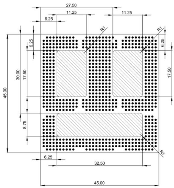
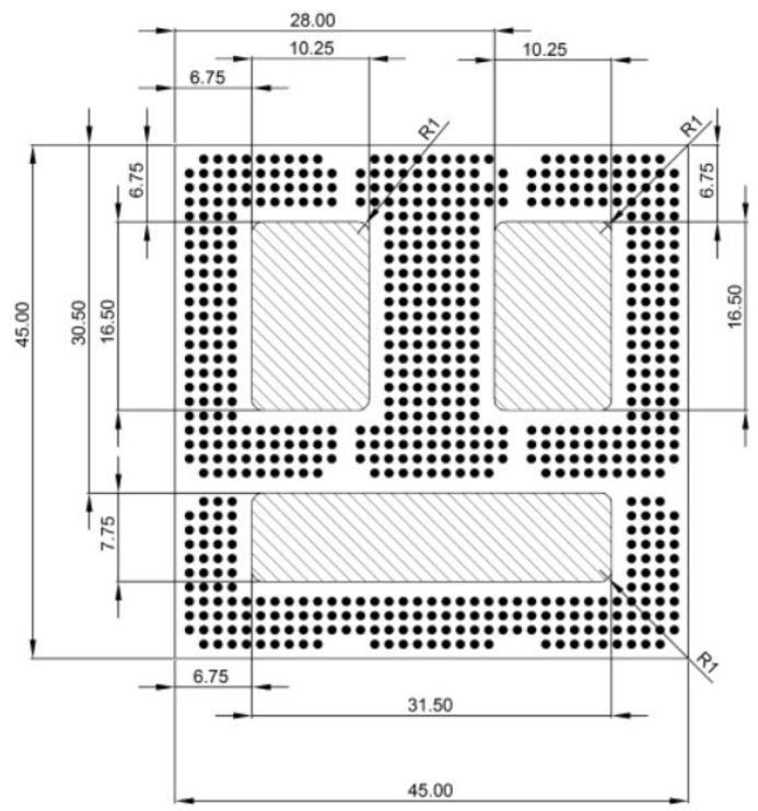
OSM L Size 45x45mm
![28.00\n10.25\n10.25\n6.75\nR1\nR1\n6.75\n45.00\n30.50\n16.50\n7.75\n16.50\n31.50\n6.75\n45.00\nR1](.osm-imx8mp-prelim-manual-50m-76100-1000-01/ac68a8495ea1b6394a43a4daab090ef7d54f5f3a677dc630b3b811a9b3b4b53e.jpg)

![27.50\n11.25\n6.25\n11.25\nR1\nR1\n6.25\n30.00\n17.50\n45.00\n8.75\n6.25\n32.50\n45.00\n17.50](.osm-imx8mp-prelim-manual-50m-76100-1000-01/c1e5f1ae8468893251531d7735b7e4cb6feee0e8d04f6710b663a29ab32e58fe.jpg)

Figure 4 – Placement area and Cut-out area – size L

# 7. Thermal Solutions

# 7.1. Heatspreader : HTS

This isn't included in the module project, as it depends on the available space on the carrier. However, a standard heat solution is provided for the ADLINK carrier, which can be reused if needed.

# 7.2. Heatsink: THS

This isn't included in the module project, as it depends on the available space on the carrier. However, a standard heat solution is provided for the ADLINK carrier, which can be reused if needed.

# 7.3. DQA

All interfaces must undergo testing and validation. Since most of the PHYs are now situated on the carrier, the assembly shall be validated. Any additional hardware on future carriers will require validation on a case-by-case basis.
[🔗 Link to the original document](.osm-imx8mp-prelim-manual-50m-76100-1000-01/osm-imx8mp-prelim-manual-50m-76100-1000-01.pdf)